
On design of multiple-valued sequential reversible circuits for nanotechnology based systems
6
On Design of Multiple-Valued Sequential Reversible Circuits for Nanotechnology Based Systems Majid Mohammadi Shahid Beheshti University Tehran, Iran [email protected] Mohammad Eshghi Shahid Beheshti University Tehran, Iran [email protected] Majid Haghparast Science & Research Branch Islamic Azad University haghparast@Sr. iau.ac. ir Abstract Multiple-valued reversible logic is an emerging area in reversible and quantum logic circuit synthesis. Multiple-valued reversible logic circuits can potentially reduce the width of the reversible or quantum circuit which is a limitation in current quantum technology. In this paper we propose a method to synthesize the multiple-valued reversible sequential circuits. Implementations for ternary D and Tflip flops and edge triggered D flip flop are proposed. Synthesis of generalized fanout circuit and generalized r-valued T flip flop are also presented. Keywords: Multiple-valued logic, reversible logic, sequential circuit, genetic algorithm. 1. Introduction It is proved that irreversible circuits have power dissipations regardless of their underlying technology [1]. Binary reversible circuits have been studied in low- power CMOS design, quantum computation, nanotechnology-based systems, and optical computing. On the other hand a multiple-valued logic (MVL) reduces the width of the reversible or quantum circuit. At present, quantum implementations are limited to a small number of quantum bits (qubits). MVL coding reduces the number of qubits in the circuit, allowing for larger specifications in current technology [2]. An r-valued mxm function is reversible if and only if it maps each of input patterns to a unique output pattern [3]. Synthesis of a combinational MVL circuit implements a reversible MVL function by a cascade of reversible gates. In multiple-valued quantum circuits, the quantum digits (qudits) are the signals and quantum gates are operators, represented by unitary matrices [4,5]. Many years, the researches in reversible logic design were limited to the combinational logic circuits. To design a sequential logic circuit, it is necessary to use the feedback, which seems to violate the basic laws of reversible logic circuits. In reversible logic circuits loops was not allowed. However, Toffoli and Fredkin in 1980 in their papers, [6] and [7], presented the sequential reversible circuits. Recently, Banerjee and Pathak in [8] have shown that the feedback is not a violating condition for reversible logic circuits. A circuit is feasible by feedback if its transition function (or state transition table) remains reversible, or its transfer matrix is unitary. In this paper, a method to design the sequential MVL reversible circuits is presented. We use the genetic algorithm (GA) [9] as a synthesis tool to design and optimize these circuits. We use the generalized CNOT, Cycle, and Self shift MVL gates which Miller et al [10] have used in their combinational synthesis algorithm. The GA-based synthesis algorithm, used in this research is a simple extension of the work which is done in [11] for binary circuits. Since the MVL reversible gates are realized in quantum technology [2], the proposed method is also applicable in synthesis of quantum sequential MVL circuits. The background on MVL reversible gates is presented in section 2. GA-based synthesis method for combinational circuits is proposed in section 3. In section 4 we propose an algorithm to synthesize some basic MVL sequential circuits. 2. Multiple-valued reversible gates An r-valued gate is reversible if and only if it maps each of input patterns to a unique output pattern. As a result, a reversible gate has equal number of inputs and outputs. Two MVL reversible and quantum set of gates are used in the synthesis of MVL circuits which are realizable in existing MVL quantum technology. Generalized ternary gates (GTG) are ternary controlled 2x2 gates which are used in [12] to synthesize the ternary reversible circuits. The generalized CNOT, Cycle, and Self shift gates which are used in [10] have a simpler structure than GTG gates, and can be extended to higher-radix logic with more control inputs. In this paper we use the generalized CNOT, Cycle, and Self shift gates in our synthesis method. Fig.l shows the symbols and operations of these gates. In this figure r is radix and n (0 n < r) is the type of gate (E.g., C}, C 2 , ... ). Table 1 shows the truth table of these gates in ternary case. Note that the ternary S2 gate is equivalent to the NOT gate. The Co gate is as a buffer.
-
Upload
independent -
Category
Documents
-
view
3 -
download
0
Transcript of On design of multiple-valued sequential reversible circuits for nanotechnology based systems

On Design of Multiple-Valued Sequential Reversible Circuits forNanotechnology Based Systems
Majid MohammadiShahid Beheshti University
Tehran, [email protected]
Mohammad EshghiShahid Beheshti University
Tehran, [email protected]
Majid HaghparastScience & Research Branch
Islamic Azad Universityhaghparast@Sr. iau.ac. ir
AbstractMultiple-valued reversible logic is an emerging
area in reversible and quantum logic circuit synthesis.Multiple-valued reversible logic circuits can potentiallyreduce the width of the reversible or quantum circuitwhich is a limitation in current quantum technology. Inthis paper we propose a method to synthesize themultiple-valued reversible sequential circuits.Implementations for ternary D and Tflip flops and edgetriggered D flip flop are proposed. Synthesis ofgeneralized fanout circuit and generalized r-valued Tflip flop are also presented.
Keywords: Multiple-valued logic, reversible logic,sequential circuit, genetic algorithm.
1. IntroductionIt is proved that irreversible circuits have power
dissipations regardless of their underlying technology[1]. Binary reversible circuits have been studied in lowpower CMOS design, quantum computation,nanotechnology-based systems, and optical computing.On the other hand a multiple-valued logic (MVL)reduces the width of the reversible or quantum circuit.At present, quantum implementations are limited to asmall number of quantum bits (qubits). MVL codingreduces the number of qubits in the circuit, allowing forlarger specifications in current technology [2].
An r-valued mxm function is reversible if and onlyif it maps each of input patterns to a unique outputpattern [3]. Synthesis of a combinational MVL circuitimplements a reversible MVL function by a cascade ofreversible gates. In multiple-valued quantum circuits,the quantum digits (qudits) are the signals and quantumgates are operators, represented by unitary matrices[4,5].
Many years, the researches in reversible logic designwere limited to the combinational logic circuits. Todesign a sequential logic circuit, it is necessary to usethe feedback, which seems to violate the basic laws ofreversible logic circuits. In reversible logic circuitsloops was not allowed. However, Toffoli and Fredkin in1980 in their papers, [6] and [7], presented thesequential reversible circuits. Recently, Banerjee and
Pathak in [8] have shown that the feedback is not aviolating condition for reversible logic circuits. Acircuit is feasible by feedback if its transition function(or state transition table) remains reversible, or itstransfer matrix is unitary.
In this paper, a method to design the sequential MVLreversible circuits is presented. We use the geneticalgorithm (GA) [9] as a synthesis tool to design andoptimize these circuits. We use the generalized CNOT,Cycle, and Self shift MVL gates which Miller et al [10]have used in their combinational synthesis algorithm.The GA-based synthesis algorithm, used in thisresearch is a simple extension of the work which isdone in [11] for binary circuits. Since the MVLreversible gates are realized in quantum technology [2],the proposed method is also applicable in synthesis ofquantum sequential MVL circuits.
The background on MVL reversible gates ispresented in section 2. GA-based synthesis method forcombinational circuits is proposed in section 3. Insection 4 we propose an algorithm to synthesize somebasic MVL sequential circuits.
2. Multiple-valued reversible gates
An r-valued gate is reversible if and only if it mapseach of input patterns to a unique output pattern. As aresult, a reversible gate has equal number of inputs andoutputs. Two MVL reversible and quantum set of gatesare used in the synthesis of MVL circuits which arerealizable in existing MVL quantum technology.Generalized ternary gates (GTG) are ternary controlled2x2 gates which are used in [12] to synthesize theternary reversible circuits. The generalized CNOT,Cycle, and Self shift gates which are used in [10] have asimpler structure than GTG gates, and can be extendedto higher-radix logic with more control inputs. In thispaper we use the generalized CNOT, Cycle, and Selfshift gates in our synthesis method. Fig.l shows thesymbols and operations of these gates. In this figure r isradix and n (0 ~ n < r) is the type of gate (E.g., C}, C2,...). Table 1 shows the truth table of these gates internary case. Note that the ternary S2 gate is equivalentto the NOT gate. The Co gate is as a buffer.

in synthesis of the combinational MVL reversiblecircuits is described. In the next section the method isextended to sequential MVL reversible circuits usingstate transition table.
We use a simple extension of GA-based synthesisalgorithm proposed in [11] to synthesize the MVLreversible circuits. In GA-based synthesis algorithmsthe circuits are shown in the music line styIe. In thisstyle an n-input/output circuit is shown as n parallellines that some reversible gates are placed on them(Fig.3). Each gate is coded to a string as is shown inFig.3.
h bl fT bl 1a e : trot ta e 0 some ternary gatesinput Target output (Q)
A C1 C2 So SI S2 NOT0 1 2 0 1 2 21 2 0 2 0 1 12 0 1 1 2 0 0
A%O A~O A-$-OQ = ( A + n ) mod r Q =(( r-1) A + n ) mod r Q = NOT A
(a) (b) (c)Fig.I. Symbol and functionality of Some MVL gates: (a)
Cycle gate, (b) Self shift gate, (c) NOT gate
m gates
The Circuit: ~ $ ::: ~//)~~
Cromosome: I Gate 1 (f Gate 2 '[) ••• I Gate m
",-,,""" "",-------",;; '-"'"""
The first field indicates the type of gate. The secondfield shows the binary number of the location of themain input/output. The next 2(r-I) fields show thenumber of the location of gate's control inputs and theircorresponding threshold values. One chromosomewhich contains m gates, codes a circuit.
Firstly, we construct a population of chromosomeswhich represents the MVL reversible circuits. Thispopulation is initialized randomly. Then three operatorsof GA, namely mutation, crossover, and selection areapplied to the population of chromosomes to generate abetter population. The crossover operator selects twochromosomes randomly and exchanges some of theircorresponding segments. The mutation operator appliesrandom changes to the selected chromosome, with aspecific probability. The selection operator selects someof the good chromosomes for reproduction of the nextpopulation. Selection directs the algorithm toward theoptimum. Fig.4 shows the GA synthesis algorithm. Inselection operator we calculate a fitness function toevaluate the chromosomes. In synthesis problem, thefitness function is the Hamming distance of the outputof desired truth table and output of each circuit asshown in equation 1.
Table 2: truth table ofcontrolled ternary gatesInputs Tar~et output (Ql)
Ao Al CCI CC2 CSO CSI CNOT0 0 0 0 0 0 00 1 1 1 1 1 20 2 2 2 2 2 1I 0 0 0 0 0 01 1 1 1 1 1 11 2 2 2 2 2 22 0 ] 2 0 1 22 1 2 0 2 0 12 2 0 1 1 2 0
These gates are generalized to the controlled n xngates [10] with n-l control inputs and one target input.Some threshold values are assigned to the controlinputs. The gate applies its function to the target input ifall controls are equal to or greater than theircorresponding threshold vales.
Ao~Oo Ao~Oo Ao-,-OoA1 --§]- 0 1 A1 --§- 0 1 A1~ 0 1
(a) (b) (c)Fig.2. Controlled MVL gates: (1) Controlled Cycle gate,
(b) Controlled Self shift gate, (c) CNOT gate. P is thresholdof input.
Fig.2 shows the symbol of the 2x2 MVL controlledgates. The Ao input is control input and A I is targetinput. The P value in circle of control input (blackcircle) represents the threshold value of input. If thecontrol input (Ao) is less than the threshold (P), then thetarget output (QI) is as the input target (AI); else, thegate's function is applied to the target input (AI) togenerate a new value for the target output (QI). Qo isalways equal to Ao. Table 2 shows the truth table ofcontrolled gates (only target output) in the ternary casewith threshold value ofP = 2.
3. Using genetic algorithms in synthesis ofcombinational MVL reversible circuits
In this section, application of genetic algorithm (GA)
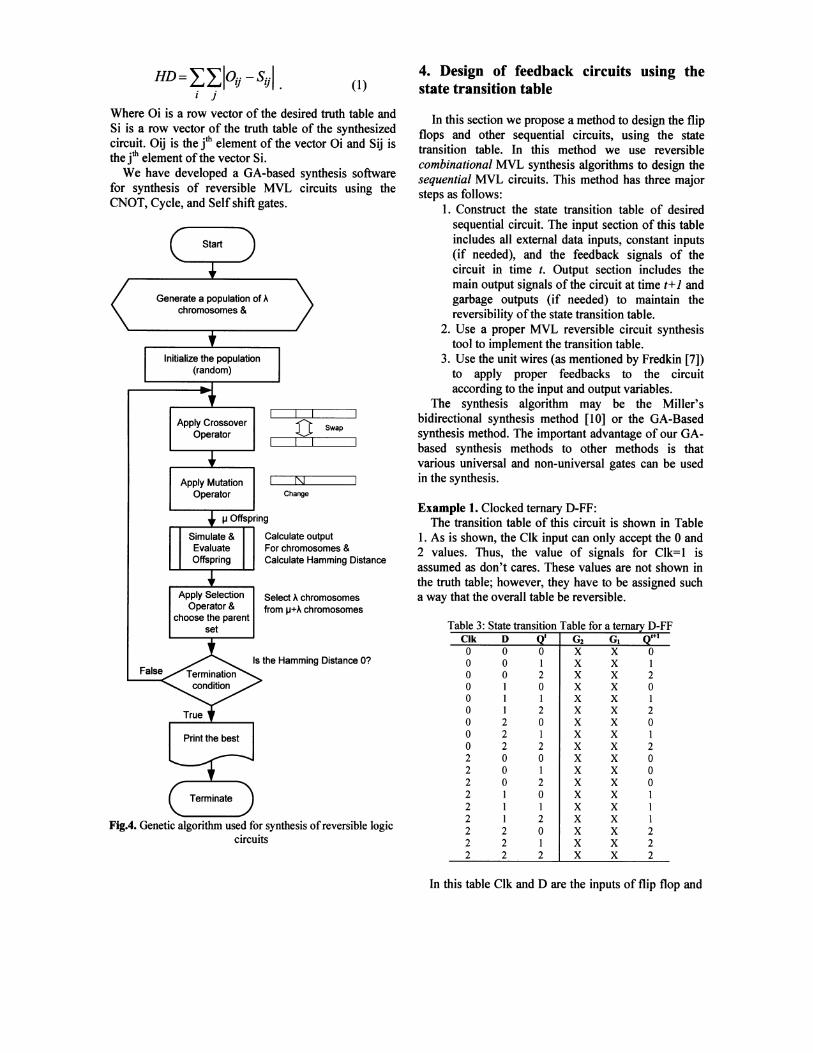
Is the Hamming Distance O?
Table 3: State transition Table for a tern D-FFelk D G2 G1
t+1
0 0 0 x x 00 0 1 X X 10 0 2 X X 20 1 0 X X 00 1 1 X X 10 1 2 X X 20 2 0 X X 00 2 1 X X 10 2 2 X X 22 0 0 x x 02 0 1 X X 02 0 2 X X 02 1 0 X X 12 1 1 X X 12 1 2 X X 12 2 0 X X 22 2 1 X X 22 2 2 X X 2
4. Design of feedback circuits using thestate transition table
In this section we propose a method to design the flipflops and other sequential circuits, using the statetransition table. In this method we use reversiblecombinational MVL synthesis algorithms to design thesequential MVL circuits. This method has three majorsteps as follows:
1. Construct the state transition table of desiredsequential circuit. The input section of this tableincludes all external data inputs, constant inputs(if needed), and the feedback signals of thecircuit in time t. Output section includes themain output signals of the circuit at time t+1 andgarbage outputs (if needed) to maintain thereversibility ofthe state transition table.
2. Use a proper MVL reversible circuit synthesistool to implement the transition table.
3. Use the unit wires (as mentioned by Fredkin [7])to apply proper feedbacks to the circuitaccording to the input and output variables.
The synthesis algorithm may be the Miller'sbidirectional synthesis method [10] or the GA-Basedsynthesis method. The important advantage of our GAbased synthesis methods to other methods is thatvarious universal and non-universal gates can be usedin the synthesis.
Example 1. Clocked ternary D-FF:The transition table of this circuit is shown in Table
1. As is shown, the elk input can only accept the 0 and2 values. Thus, the value of signals for Clk=1 isassumed as don't cares. These values are not shown inthe truth table; however, they have to be assigned sucha way that the overall table be reversible.
(1)
I IApply Crossover D Swap
OperatorI I
Apply Mutation NOperator Change
Apply Selection Select }.. chromosomesOPerator & from IJ+}.. chromosomes
choose the parentset
IJ Offspring
Simulate & Calculate outputEvaluate For chromosomes &Offspring Calculate Hamming Distance
Generate a population of }..chromosomes &
Fig.4. Genetic algorithm used for synthesis ofreversible logiccircuits
HD= IIIOij -Sijl.i j
Where Oi is a row vector of the desired truth table andSi is a row vector of the truth table of the synthesizedcircuit. Oij is the Jh element of the vector Oi and Sij isthe jth element of the vector Si.
We have developed a GA-based synthesis softwarefor synthesis of reversible MVL circuits using theCNOT, Cycle, and Self shift gates.
In this table Clk and D are the inputs of flip flop and

Qt is the past value of the feedback output at time t. Qt+lis the main output and G1 and G2 are the garbageoutputs. Garbage outputs are some outputs which areadded to the truth table to maintain the reversibility ofthe function. Since the number of inputs of Table 3 is 3,at least two garbage outputs have to be added to thetable. Generally, if maximum repetition of patterns inthe output is A, at least 11 garbage outputs are needed tomake the truth table reversible; as is shown in equation2 (r is radix).
1] = fLoBr Al (2)
Although, the values of the garbage outputs are notimportant, they have to be assigned such a way that thereversibility condition is maintained. The values ofthese garbage outputs affect on the synthesized circuit.Determining the optimal value for these outputs is anopen problem in MVL reversible logic synthesis. In thisexample, we assumed G1=D and G2=CLK.
The GA synthesis algorithm has generated a circuitfor D-FF shown in Fig.5.a. A smaller circuit is obtainedusing the Cycle gates which is shown in Fig.5.b. Inthese figures we have also applied the feedback signals,shown as dotted lines with the bold arrows.
G
--~--....---G(a)
:···················.···················1. .Lot at~.~j
o ....._ -G
Clk--~-- - G
(b)Fig.5. Synthesis of ternary clocked D-FF (a) using Self shift
and CCNOT gates (b) using Cycle gates.
Any output of a reversible or quantum gate can driveonly one input of another gate. That is, the fanout for areversible gate is 1. Consequently, to copy the Qt+lsignal as the output of the flip flop, we have to use afanout circuit. We use the GA synthesis algorithm todesign this circuit. Table 4 shows the fanout truth table.In this table when Ao is '0', the Qo and Ql are equal toAo• Other states are don't care conditions which weassign some values to keep the reversibility of thefunction. The Ao input is a constant input. In thesynthesis process the values of constant inputs is alsoimportant. In fanout circuit the '0' value results asimpler circuit. The synthesized circuit is shown inFig.6.a. Fig.6.b shows the synthesized 4-valued(quaternary) fanout circuit. The regularity of these twocircuits leads us to a generalized r-valued fanout circuit
which is shown in Fig.6.c.
Table 4: Truth table of fanout circuit.Al AO QI QOo 0 0 0o I I Io 2 2 2lOX XI I X XI 2 X X2 0 X X2 I X X2 2 X X
Ao~ 0 0 Ao~ Qo=Ao
A1=O §@} Q1 A1=O~ Q1=Ao
(a) (b)A __t-I.---~__ Oo=A
Q1=A
(c)Fig.6. Fanout circuit copies Aoto outputs Qo and Ql when
A1=O: (a) Ternary circuit, (b) Quaternary circuit(c) Generalized r-valued circuit
Fig.7 shows the complete ternary clocked D-FF inwhich the fanout circuit is also embedded. As Fredkinin [7] mentioned, the wire which connects Qt+1to Qt is aunit wire with a specific delay. This delay is the timedifference of the Qt and Qt+1 signals. It is necessary insome sequential circuits to let the clock signal return to'0' before a change in the state of the Qt. For examplewe can use a 1x 1 gate to generate a delay. The fanoutcircuit has also a delay which is considered as the unitdelay in the feedback path.Example 2. T-FF:
The summary of transition table of T-FF is shown inTable 2. If we set the elk and T signals to 2, the outputof T-FF (Qt+1
) is the unit Cycle of its previous value(Qt). Since the value of' l' for Clk input is not allowed,the output vales are considered as don't care conditions.As the D-FF, the truth table of the T-FF has also twogarbage outputs.
~.....~~:~._-,l Qtg1C1 Qt+2J
o Cz cz G
elk G
Fig.7: Clocked D-FF with fanout circuit to copy the Qt+loutput.
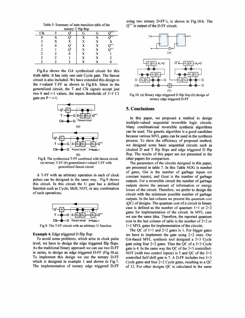
Table 5: Summary of state transition table of theternary T fli flo
using two ternary D-FF's, is shown in Fig.lO.b. TheQt+1 is output of the D-FF circuit.
o Q Q
Qt~+~ c, c, ~:~· .· .· .· .· .· .
(a)
o Qo
In this paper, we proposed a method to designmultiple-valued sequential reversible logic circuits.Many combinational reversible synthesis algorithmscan be used. The genetic algorithm is a good candidatebecause various MVL gates can be used in the synthesisprocess. To show the efficiency of proposed method,we designed some basic sequential circuits such asclocked D and T flip flops and edge triggered D flipflop. The results of this paper are not presented in theother papers for comparison.
The parameters of the circuits designed in this paper,are presented in table 7. In this Table NaG is numberof gates, Gin is the number of garbage inputs (orconstant inputs), and Gout is the number of garbageoutputs. For a reversible circuit the number of garbageoutputs shows the amount of information or energylosses of the circuit. Therefore, we prefer to design thecircuit with the minimum possible number of garbageoutputs. In the last column we present the quantum cost(QC) of designs. The quantum cost of a circuit in binarycase is defined as the number of quantum 1x1 or 2x2gates for implementation of the circuit. In MVL casewe use the same idea. Therefore, the reported quantumcost in the last column of table is the number of 2x2 orlxl MVL gates for implementation of the circuits.
The QC of 1x1 and 2x2 gates is 1. For bigger gateswe have to implement the gate using 2x2 ones. OurGA-based MVL synthesis tool designed a 3x3 Cyclegate using four 2x2 gates. Thus the QC of a 3x3 Cyclegate is 4. In the same way the QC of the 3x3 controlledNOT (with two control inputs) is 5 and QC of the 3x3controlled Self shift gate is 7. A D-FF includes two 3x3Cycle gates and four 2x2 Cycle gates, resulting to a QCof 12. For other designs QC is calculated in the same
(b)Fig.10. (a) Binary edge triggered D flip flop (b) design of
ternary edge triggered D-FF
o ..............-GClk~-----l--""'--+-II-o+----__""""~G
5. Conclusions
(a)
T
Clk
(b)Fig.8. The synthesized T-FF combined with fanout circuit
(a) ternary T-FF (b) generalized r-valued T-FF withgeneralized fanout circuit
Example 4. Edge triggered D flip flop:To avoid some problems, which arise in clock pulse
level, we have to design the edge triggered flip flops.As the traditional binary approach we can use two D-FFin series, to design an edge triggered D-FF (Fig. 1O.a).To implement this design we use the ternary D-FFwhich is designed in example 1 and shown in Fig.7.The implementation of ternary edge triggered D-FF
o X ~ X X ~1 X X X X X2 0 Qt X X Qt+l2 1 Qt X X Qt+l2 2 0 X X 12 2 1 X X 22 2 2 X X 0
Fig.8.a shows the GA synthesized circuit for thistruth table. It has only one unit Cycle gate. The fanoutcircuit is also included. We have extended this design tothe r-valued T-FF as shown in Fig.8.b. Since in thegeneralized circuit, the T and Clk signals accept justtwo 0 and r-l values, the inputs thresholds of 3x3 Clgate are P = r-l.
f·········......····························iLot I-------------~•.:
T
Clk
Fig.9. The T-FF circuit with an arbitrary U function.
A T-FF with an arbitrary operation in each of clockpulses can be designed in the same way. Fig.9 showsthis circuit. In this circuit the U gate has a definedfunction such as Cycle, Shift, NOT, or any combinationof such operations.

manner.
Table 7: parameters of circuits are desi ned in this aperName NOG Gin Gout QC
Clocked D-FF 6 I 2 12Clocked ternary T-FF 3 1 2 6Clocked r-val. T-FF r 1 2 r + 3
Ed e-Tri . D-FF 13 2 3 25
6. References
[1] R. Landauer, "Irreversibility and heat generation inthe computing processes" IBM J. Res. Develop.July 1961.
[2] Muthukrishnan, A., Stroud, Jr., C. R. (2000).Multivalued logic gates for quantum computation.Physical Review A, Vol. 62, No.5, 052309/1-8.
[3] AI-Rabadi, A., "New Multiple-Valued Galois FieldSum-of-Product Cascades and Lattices forMultiple-Valued Quantum Logic Synthesis," 6thInt. Symp. on Representations and Methodology ofFuture Computing Technologies, March 2003, pp.171-182.
[4] Khan, Mozammel H. A., Marek A. Perkowski andPavel Kerntopf, "Multi-output Galois Field Sum ofProducts (GFSOP) Synthesis with New QuantumCascades," Proc. International Symposium onMultiple-Valued Logic, May 2003, pp. 146-153.
[5] Picton, P., "A Universal Architecture for MultipleValued Reversible Logic," MVL Journal, 5,2000,pp.27-37.
[6] T. Toffoli, "Reversible computing", Tech memoMIT/LCS/TM-151, MIT Lab for ComputerScience (1980).
[7] E. Fredkin, T. Toffoli "Conservative logic", Int. J.Theo. Phys., 21 (1982) 219.
[8] Anindita Banerjee, Anirban Pathak "On theSynthesis of Sequential Reversible Circuit"arXiv:0707.4233v1 [quant-ph] 28 Jul2007
[9] Goldberg, D. E. (1989). "Genetic Algorithms inSearch, Optimization, and Machine Learning".Addison Wesley.
[10] Miller, D. M., D. Maslov, and G. W. Dueck,"Synthesis of Quantum Multiple-Valued Circuits,"Journal of Multiple-Valued Logic and SoftComputing, submitted Feb. 2004.
[11]M.Mohamadi, M.Eshghi, K.Navi, "Optimizing theReversible Full Adder Circuit", IEEE EWDTS,Yerevan, Sep.7-10,2007, pp. 312-315
[12] Mozammel H. A. Khan and Marek Perkowski,"Genetic algorithm based synthesis of multi-outputternary functions using quantum cascade ofgeneralized ternary gates" IEEE Congress onEvolutionary Computation, 2004. CEC2004.