'Godspell' starts new era of Spring plays with musical favorite

ARTICLE IN PRESS
Nuclear Instruments and Methods in Physics Research A 610 (2009) 1–10
Contents lists available at ScienceDirect
Nuclear Instruments and Methods inPhysics Research A
0168-90
doi:10.1
� Corr
E-m
journal homepage: www.elsevier.com/locate/nima
Nanotechnology: A new era for photodetection?
M. Ambrosio a,�, A. Ambrosio a,b, G. Ambrosone a,b, L. Campajola a,b, G. Cantele a,b, V. Carillo a,b,U. Coscia a,b, G. Iadonisi a,b, D. Ninno a,b, P. Maddalena a,b, E. Perillo a,b, A. Raulo a,b, P. Russo a,b, F. Trani a,b,E. Esposito a,c, V. Grossi a,d, M. Passacantando a,d, S. Santucci a,d, M. Allegrini a,e, P.G. Gucciardi a,f,S. Patane a,g, F. Bobba a,h, A. Di Bartolomeo a,h, F. Giubileo a,h, L. Iemmo a,h, A. Scarfato a,h, A.M. Cucolo a,h
a INFN Sezione di Napoli, Via Cintia 2, 80125 Napoli, Italyb Dipartimento di Fisica, Universita ‘‘Federico II’’ di Napoli, Italyc Istituto di Cibernetica ‘‘E. Caianiello’’, Italyd Dipartimento di Fisica, Universita dell’Aquila, Italye Dipartimento di Fisica, Universia di Pisa, Italyf CNR—IPCF Sezione di Messina, Italyg Dipartimento di Fisica della Materia and TFA, Universita di Messina, Italyh Dipartimento di Fisica, Universita di Salerno, Italy
a r t i c l e i n f o
Available online 29 May 2009
Keywords:
Carbon nanotube
Photodetector
Field emission
02/$ - see front matter & 2009 Elsevier B.V. A
016/j.nima.2009.05.138
esponding author.
ail address: [email protected] (M. Ambrosio
a b s t r a c t
Nowadays we live in the so-called ‘‘Silicon Era’’, in which devices based on the silicon technology
permeate all aspects of our daily life. One can simply think how much silicon is in the everyday
household objects, gadgets and appliances.
The impact of silicon technology has been very relevant in photodetection as well. It enables
designing large or very large-scale integration devices, in particular microchips and pixelled detectors
like the Silicon Photo Multiplier made of micrometric channels grouped in mm2 pixels. However, on the
horizon, the recent development of nanotechnologies is opening a new direction in the design of sub-
micron photodevices, owing to the capability to deal with individual molecules of compounds or to
chemically grow various kinds of materials.
Among them, carbon compounds appear to be the most promising materials being chemically very
similar to silicon, abundant and easy to handle. In particular, carbon nanotubes (CNT) are a very
intriguing new form of material, whose properties are being studied worldwide providing important
results.
The photoelectric effects observed on carbon nanotubes indicate the possibility to build
photodetectors based on CNTs inducing many people to claim that we are at the beginning of a Post
Silicon Era or of the Carbon Era.
In this paper, we report on the most important achievements obtained on the application of
nanotechnologies to photodetection and medical imaging, as well as to the development of radiation
detectors for astro-particle physics experiments.
& 2009 Elsevier B.V. All rights reserved.
1. Introduction
The birth of Silicon Era usually is referred to the year 1958,when Jack Kilby, Nobel Price 2000, created the first integratedcircuit at Texas Instruments to prove that resistors and capacitorscould exist on the same piece of semiconductor material. Hiscircuit consisted of a sliver of germanium with five componentslinked by wires. This has been the first integrated circuit whosebackbone was the silicon wafer in which the circuit was directlycarved. This approach opened the way to make more powerful,
ll rights reserved.
).
smaller and cheaper electronics devices. Starting from thisachievement, the modern world has been fully based on silicontechnology, by which every aspect of our life is imbibed: internet,computers, television, integrated circuits, but also pace-makers,solar energy, artificial prothesis, digital camera, GPS navigator, etc.Starting from raw silicon, we can produce silicon wafers, applylithographed masks, carve inside and obtain electronic chips forour electronic devices with lower and lower costs and highercapabilities. To date, microelectronics has developed according toMoore’s law stating that every two years the number of transistorin a chip doubles while the cost halves.
From the point of view of photodetection, the most advancedby-product of silicon technology is the silicon photomultiplier(SiPM), a single photon detector made of silicon pixels, as small as

ARTICLE IN PRESS
M. Ambrosio et al. / Nuclear Instruments and Methods in Physics Research A 610 (2009) 1–102
40mm2, grouped in arrays a few square centimetres wide [1]. SiPMis able to detect individual photons and multiply the correspond-ing photoelectron through the silicon substrate up to a factor 105,producing in this way a detectable signal. SiPMs need stilladditional developments: they present great thermal noise andlow efficiency in the UV wavelength region, but they are availableon the market, and thus are relatively cheap and ready to beintensively used for applications. In the medical diagnostics, oneof the best achievement is MEDIPIX 2, the chip that allows X-raydetection of organic materials with a pitch of 55mm. In a1.4�1.6 cm2 area, 256�256 readout channels are allocated.
In April 2007, Intel presented the Xeon Family Processor(PENRYN) based on transistor with 45 nm gate. With roughlytwice the density of Intels 65 nm technology, Intel’s 45 nmcontains about twice the number of transistors into the samesilicon space, i.e. more than 400 million transistors for dual-coreprocessors and more than 800 million for quad-core ones.
So far Gordon Moore’s law is still appliable; however, physicallimits appear at the horizon. First of all, the silicon semiconductorcannot efficiently transport current in thinner matter layers owingto quantum effects, which become non-negligible; moreover jouleeffect in the electron transport produces a high amount of heat tobe dispersed. As thinner is the material layer as difficult is to avoiddamages produced by heat production in the current transportthrough the material. In addition, silicon must be producedstarting from its mineral compounds in the form of a pure block ofmaterial, then cut in wafer substrates on which lithographed maskis applied. Finally the wafer is chemically managed to take awaythe non-impressed material. The process is long and highlyspecialized. Very complex software packages must be used todesign details of chips and the final production cost is non-negligible.
On the other hand, 100 nm is at the border of nanotechnology.That means the need is to control matter at the molecular–atomiclevel during the fabrication of devices or materials within this sizerange. With nanotechnology, the building process inverts thetop–down process on which the use of silicon compounds isbased. Macro structures can be built by chemically assemblingindividual molecules or by stimulating the self-assemblingproperties of organic materials. In this way, dimensions ofstructures can be sub-micrometric and as large as desired: it issufficient to stop the growth process as the structure reaches thedesired dimensions.
The birth of nanoscience is commonly attributed to RichardFeynman, the physicist who in a famous speech given at theAmerican Physical Society meeting at Caltech on December 29,1959 claimed: ‘‘The future is in the smaller things’’. He introducedthe concept of nanotechnology as the controlled manipulation ofmatter at the nanometer length scale suggesting that ‘‘There’s a
plenty of room at the bottom’’. Since then, thousands of physicistsapplied to nanoscience. New materials have been created and thenew physics phenomena observed in the nanoscale opened a newscenario on the future of science and technology.
2. Carbon nanotubes
Since 15 years, a new material has been continuouslyincreasing its importance: carbon in the form of nanotubes.Carbon is present in nature in several allotropic forms. The mostwell-known are graphite and diamond. In 1985, the discovery offullerene opened a new scenario: carbon can be assembled in thenanoscale as tiny droplets of graphene. The C60 structures, 7.1 Aradius, were produced by arc discharge [2]. Six years later,graphene sheets rolled up as tubes with nanometer diameter,tens of micron long, were produced with similar chemical process
first as multiwalled carbon nanotubes (MWCNT) [3], then assingle wall carbon nanotubes (SWCNT) [4]. Their structure’sproperties are fully determined by the chiral indexes of rollingprocess [5]. From those, CNT diameter is fixed, as well as electricalproperties, i.e. they will be metallic or semimetallic or semi-conductors according to the chiral indexes.
Depending on the specific interests, and targeted applications,nanotubes are regarded as either single molecules or quasi-one-dimensional crystals with translational periodicity along the tubeaxis. As there are an infinite number of ways of rolling a sheet intoa cylinder, the large variety of possible helical geometries definingthe tube chirality provides a family of nanotubes with differentdiameters and microscopic structures. This dependence on theatomic configuration is quite unique in solid-state physics.
Applications of carbon nanotubes range from reinforcement ofcomposites or conductive plastics to electrodes for batteries or flatscreens, field effect transistors, chemical or force sensors andelectromechanical memory. These applications have been demon-strated in bulk as well as on surfaces and on individual tubes.
A very large literature has been published on the properties ofCNTs. Their very peculiar properties have been intensivelyinvestigated everywhere in the world and thousands of research-ers produce, study and manipulate CNTs in a number of ResearchLaboratories. Most of them are convinced that the Post Silicon ERAhas turned into the carbon ERA.
From the point of view of photodetection, semiconductingnanotubes show interesting optoelectronic properties in theregion of near-to-mid infrared (from �1 to �15mm) tied to theirelectronic characteristics. Due to their quasi-1D structure,SWCNTS feature quasi-discrete energy levels rule by van Hovesingularities in the density of states. The energy gap is a functionof the diameter, as approximately given by the relationship:Egap ¼ a/d, where a ¼ 0.0284 eV nm and d is the diameter in nm.This implies that for the SWCNT, with diameter from about 1 to2 nm, the fundamental gap (eh11) varies from 0.4 to 0.7 eV,corresponding to a wavelength range from 1.5 to 3mm [6]. A layerof multiwall carbon nanotubes covers instead a wide range ofdiameters and chiralities whose characteristics have not yet beenfully understood, offering a device sensitive to a wide range ofwavelength frequencies, from 200 nm up to several microns.
The capability of CNTs to detect radiation has been demon-strated by various authors [7,8] who measured a variation in thenanotube’s conductivity when illuminated with IR radiation. Thepioneering work of Xu [7] suggested the possibility of realizinguncooled bolometers for space physics made of CNT. Photocon-ductivity of individual, ropes and films of CNTs has been alsoinvestigated in the visible [9] and IR [10] spectral regions. Photoninduced charge carrier generation in single wall carbon nanotubesand subsequent charge separation across the metal–carbonnanotube contacts is believed to cause the photoconductivityvariations [9]. Mesurements in the UV region, to the best of ourknowledge, are still missing.
In this scenario, the Italian National Institute for NuclearPhysics (INFN) promoted the gruppo INFN per le nano tecnologie(GINT) collaboration with the aim to explore the CNT propertiesand their potential application to photodetection.
3. The GINT (gruppo INFN per le nanotecnologie) activity
The GINT collaboration was born in 2005 and has been fundedby INFN on the base of an activity program three years long. Thecollaboration actually consists of 41 physicists from 6 ItalianUniversities and several other scientific institutions. Activitiesstarted in January 2006 with the aim to explore the possibilityof using carbon nanotube-based devices to provide new

ARTICLE IN PRESS
M. Ambrosio et al. / Nuclear Instruments and Methods in Physics Research A 610 (2009) 1–10 3
opportunities for obtaining large-area and highly sensitiveradiation detectors.
The question has been addressed investigating the nanotubes’behaviour in different conditions with a number of differentdiagnostic methods. In the following, we summarize the mainitem and most significant results obtained.
3.1. Nanotubes production
The first aim was the development of an improved process togrow carbon nanotubes on various substrates with differentgeometry using chemical vapour deposition (CVD) [11]. Fig. 1shows two types of nanotubes grown at different CVDtemperatures. On the left side (T ¼ 500 1C), the crystallinestructure of nanotubes is not yet well developed and the tubeslook like carbon nanofibers. On the right side (T ¼ 700 1C), instead,a clear one-dimensional and crystalline structure is visible. CNTsare well aligned, with uniform density and uniform length ofabout 20mm. The substrate is a 1�1 cm2 silicon, 500-mm-thick,and CNTs cover uniformly the entire surface.
TEM images carried out by high resolution transmissionelectron microscopy (HRTEM, JEOL JEM 2010) of both kinds of
Fig. 1. Left: carbon nanotubes grown by CVD at a te
Fig. 2. (a) Structure of a 500 1C carbon nanotubes; (b) nickel c
CNTs are reported in Fig. 2. Nanotubes grown at low temperaturepresent an average length of 150 nm, a diameter of tensnanometers and a round edge of 20–30 nm. The structure ismore similar to a filled cylinder than to a tube, with the externalshell not well graphitized (Fig. 2a). Nickel particles used ascatalyst appear to be encapsulated close to the apex of thestructure (Fig. 2b).
At 700 1C temperature, the CVD process produces nanotubes ofvery different kinds. Their structure is well defined as a multiwallmade in average of 10–15 tubes, with an inner diameter of5–10 nm, an outer diameter ranging from 15 to 25 nm (Fig. 3a andb) and a length of tens of micron. Several tubes look bended.Inclusions of particles are also present (Fig. 3c). Most of them areuncapped (Fig. 3d).
3.2. Raman spectroscopy
Complementary structural investigations have been carriedout by micro-Raman spectroscopy [12]. While HRTEM featuresunique imaging capabilities, Raman spectroscopy has the advan-tage of being a noninvasive technique suitable for in-situ, real-time analysis of carbon-based materials and devices [13–16].
mperature of 5001; Right: CNT growth at 7001.
atalyst particle encapsulated at the apex of the structure.

ARTICLE IN PRESS
Fig. 3. TEM images of 7001 of CNTs.
M. Ambrosio et al. / Nuclear Instruments and Methods in Physics Research A 610 (2009) 1–104
Typical Raman spectra of CNTs include three characteristicregions: the radial breathing modes (RBM—50ooo400 cm�1)indicating the radial in-phase motion of C atoms; the disorder-induced band (D modes-1200ooo1400 cm�1) due to structuraldefects and substitution impurities and G modes (HEM—1450ooo1650 cm�1) measuring the breaking of symmetry of graphenedue to tangential vibrations.
Fig. 4 (red line) shows the Raman spectrum of an MWCNTsample grown at 700 1C. We observe the D and the G bands(1300–1400 and 1530–1640 cm�1, respectively) typical of carbonmaterials, together with the fingerprint of the silicon substrate(520 and 980 cm�1). Compared to amorphous carbon nanofibers(Fig. 4, black line), the MWCNTs show a much narrower Dband (full-width at half-maximum of 72 against 263 cm�1), aswell as a strong 2D mode at 2653 cm�1. Both elements indi-cate a good degree of graphitization, but still there is a presenceof a non-negligible amount of defective polycrystalline carbonsites.
3.3. Field emission of CNTs
Owing to their high aspect ratio, extremely small radius ofcurvature, unique electric properties, high chemical stability andmechanical strength, carbon nanotubes can be extraordinary fieldemitters and interest in their applicability for field emission (FE)devices has been steadily growing since their discovery.
FE occurs when electrons tunnel out a solid through thesurface potential barrier whose width is reduced by the applica-tion of an external electric field. The emission current depends onthe electric field at the emitter surface, ES, and on the work-function, F, i.e. the effective surface-vacuum barrier height. The‘‘elementary’’ Fowler–Nordheim (F–N) model, derived for a flatmetallic surface at 0 K assuming a triangular potential barrier,predicts the following exponential behaviour of the emittedcurrent:
I ¼ aE2eff expð�b=Eeff Þ

ARTICLE IN PRESS
Fig. 4. Raman spectrum of MWCNTs (red line) compared to amorphous carbon
nanofibers (black line).
Fig. 5. (a) AFM probe used as counter-electrode (anode) for the measurement of
the FE current from a vertically aligned array of MWCNTs. The whole apparatus
consists of a vacuum chamber hosting an AFM/STM connected to an external
source measurement unit; (b) Field emission current versus bias voltage in (b)
logarithmic scale.
Fig. 6. The lift-off process used for CNT growth patternization.
M. Ambrosio et al. / Nuclear Instruments and Methods in Physics Research A 610 (2009) 1–10 5
where Eeff is the effective field at the emitter surface, and a and b
are constants related to the geometry and to the workfunction.CNTs are very good emitters because the coefficient correspondsto the ratio h/r where h is the nanotube length (410mm) and r isthe nanotube radius (�10 nm). The maximum current from asingle MWNT is 0.2 mA [17] For this reason, CNTs are used for newmonitors and X-ray sources.
For the measurement of the FE current, we used thenanometric probe of a high vacuum omicron AFM/STM systemas anode; the voltage was applied and the current was measuredby means of a source-measurement unit (SMU) of a Keithley4200-SCS. A detailed scheme of the apparatus is shown in Fig. 5a.The sharp metal-coated polysilicon probe (of conical shape,height�25mm, aperture of 301 and curvature radius ro35 nm)enables local FE measurements over a limited circular region(whose radius is less than 1mm) containing at most few hundredCNTs. Furthermore, the sub-micrometric inter-electrode distancelet achieve high electric fields (up to 250 V/mm) with a modestvoltage source. Voltage sweeps were performed on the allowedvoltage range up to +210 V and the current flowing through the tipwas measured with an accuracy better that 1 pA. Measurement athigh vacuum �10�8 mbar and at d E2mm is shown in Fig. 5b.After an electrical stress, consisting of a few voltage sweeps,necessary to stabilize the emission, a series of 5 sweeps isrecorded. Some negligible sweep-to-sweep variations are found,while less-noisy curves are observed with respect to theanalogous measurements performed at a lower vacuum [18].
3.4. Nanolithography and patternization
In order to grow the carbon nanotubes with a definite pattern,we have developed a procedure based on a lift-off process. ‘‘Lift-off’’ is a method for making metallic patterns on a substrate,especially for those noble-metal thin films such as platinum,tantalum, nickel or iron, which are difficult to be etched byconventional methods. The general lift-off process is as follows:first a pattern is defined on a substrate using photoresist. A film,usually metallic, is deposited all over the substrate, covering thephotoresist and areas in which the photoresist has been cleared.During the actual lifting-off, the photoresist under the film isremoved with a solvent, taking the film with it, and leaving onlythe film that was deposited directly on the substrate. In this waythe assisting material layer is exposed (Fig. 6a). This layer is then
wet-etched so as to undercut the resist (Fig. 6b). The metal issubsequently deposited on the wafer, by a thermal evaporationprocess (Fig. 6c). The resist is removed taking away the unwantedmetal with it. The assisting layer is then stripped off too, leavingthe metal pattern alone (Fig. 6d). The dimension of our patternspreads from 10mm down to 100 nm. This is obtained with anElectron Beam Lithography system.
Fig. 7 reports some results obtained with the combined use ofnanolithography and lift-off process. A square matrix of 10�10pixels, 4� 4mm2 each, is shown in Fig. 7a; pixels are made of adense layer of nanotubes, as shown in Fig. 7b, and can assume thedesired form, for example the INFN logo shown in Fig. 7c. What isimportant is that nanotubes grow only where the lift-off processleft the catalyst: no carbon compounds appear to be presentoutside the pixel, as shown in Fig. 7c.

ARTICLE IN PRESS
Fig. 7. (a) A square CNT matrix of 10�10 pixels,4� 4 mm2 obtained with a lift-off process on lithographed mask; (b) individual 2�2mm2 CNT pixel; (c) the INFN logo made
of CNT in micrometric scale; (d) Raman image of CNT and silicon substrate.
M. Ambrosio et al. / Nuclear Instruments and Methods in Physics Research A 610 (2009) 1–106
3.5. Sensitivity to the radiation
In order to investigate the sensitivity of carbon nanotubes tothe radiation, MWCNTs have been grown by CVD at a temperatureof 750 1C on a sapphire substrate as shown in Fig. 8a (black area inthe centre). Two electrodes have been obtained by platinumdeposition on the CNT layer. Fig. 8b shows the transmittancecurve for two different samples obtained by means of acommercial UV/NIR Spectrometer. The sapphire transmittance
curve is also reported. The different behaviour is due to thedifferent CNT density. In Fig. 8c, the absorbance curve indicates astrong adsorption peak at around 5 eV, which is close to the pplasmon frequency in carbon materials such as graphite, C60 andSWNTs [19].
The photosensitivity of CNTs has been investigated alsomeasuring the photocurrent collected at the two electrodesobtained illuminating the samples with monochromatic radiationin the UV–VIS–NIR range. Photocurrent normalized to the number

ARTICLE IN PRESS
Fig. 8. (a) Image of the sample used to measure the MWCNT responsivity; (b) transmittance curve of two samples; (c) the absorbance curve of samples.
1.00.4
0.8
1.2
1.6
2.0
2.4
small area whole area
Photon energy (eV)
I nor
X 1
0-21 (
As)
0.2
0.3
0.4
0.5
0.6
0.7
0.8
0.9
Absorbance
abso
rban
ce
1.5 2.0 2.5 3.0 3.5 4.0
Fig. 9. Photocurrent normalized to the number of photons Inor vs. photon energy, obtained illuminating the whole surface of an MWCNT sample with filtered light (’) as
well as small part of the surface with laser spots (x). Continuous line indicates the absorbance spectrum of the same MWCNT sample.
M. Ambrosio et al. / Nuclear Instruments and Methods in Physics Research A 610 (2009) 1–10 7
of photons Inor vs photon energy, at a polarization voltageVpol ¼ 160 V, obtained illuminating the whole surface of anMWCNT sample with filtered light (’) as well as small part ofthe surface with laser spots (x) of 1.96, 2.81 and 3.82 eV as shown
in Fig. 9. Continuous line indicates the absorbance spectrum A ofthe same MWCNT sample. Inor increases with increasing thephoton energy from the ultraviolet towards the near-infraredregion according to the results reported by others [20] in the

ARTICLE IN PRESS
M. Ambrosio et al. / Nuclear Instruments and Methods in Physics Research A 610 (2009) 1–108
1.5–3.8 eV range. It is worth observing that the measurementsperformed by laser irradiation of a small part of the samplesurface far from the Au contacts show that the photocurrent isproduced only by the MWCNTs. The photocurrent values havebeen multiplied by a scaling factor that takes into account Vpol andthe illuminated area.
3.6. Sensitivity to pulsed light: a CNT detector prototype [21]
The CNT detector layout is shown in Fig. 10. MWCNTs havebeen grown by chemical vapour deposition (CVD) on a sapphiresubstrate in the 100mm space between two comb-like electrodesmade of gold and platinum, 250-nm-thick, 100-mm-large. Thedetector prototype is 4 mm large, 6 mm long, 0.5 mm thick. Theinert sapphire substrate prevents the contribution of othermaterials to the photoresponsivity of MWCNTs and permits thestudy of the behaviour of the pure nanotube layer. On the left ofFig. 10, the structure of the electrodes is shown. In between theplatinum electrodes, the CNT black layer is clearly visible.Nanotubes have been grown using nickel nanospheres ascatalyst deposited on a silicon nitrate layer, 30-nm-thick, andsubmitted to the CVD process at a temperature of 500 1C. Theresulting nanostructures obtained are shown in the right of thefigure.
An Nd–Yag laser beam, 410 ns pulse duration, 10 Hz repetitionrate at three different wavelengths, 1064, 532 and 355 nm(respectively fundamental, second and third harmonic of theneodymium laser), is addressesd on the detector and a voltageranging between �25 and +25 V is applied to the electrodes. Thesesignals can then be easily observed by means of an oscilloscopeclosed on its load resistance of 50O without any furtheramplification, as shown in the bottom of Fig. 10. By integratingthe signals acquired using the oscilloscope over the monitoredtime window, the charge generated in the photoconversionprocess can be easily measured.
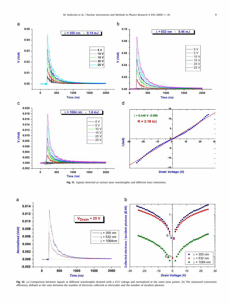
Fig. 11 shows signals detected at various laser wavelenghts anddifferent laser intensities. For each plot, a, b and c signals atvarious values of drain voltage are compared. It can be seen that inall cases, signal peak value as well as the signal charge increaseswith the voltage value in a linear relation. This suggests that thedetector is not collecting the full charge generated in thephotoconversion process, but it runs with a very low efficiency.On the other hand, we cannot increase the value of the drainvoltage because of the considerable dark current value shown inFig. 11d: nanotubes appear to be a quasi metallic compound withan ohmic resistance of 2.18 kO.
Fig. 10. (Top) layout of CNT detector; (bottom) experimental setup.
The plot of Fig. 12a shows the comparison between signals atdifferent wavelenghts drained with 25 V voltage and normalizedat the same laser power. It appears evident that signals generatedwith UV radiation is much more intense than those induced by IRor visible light. The measured conversion efficiency, defined as theratio between the number of electrons collected at electrodes andthe number of incident photons, without taking into accountreflections, geometrical factors, etc., is plotted in logarithmic scalein Fig. 12b. This plot enhances the strong difference in thephotoconversion efficiency between UV and IR regions.
It must be noted that the CNT photoconversion efficiency inthe near IR (1064 nm) is only 2% of the conversion efficiency at355 nm. This confirms independent measurements obtained witha similar larger area device analized with a UV/NIR spectrometerand reported in Fig. 8c.
3.7. Model simulation—electron affinity and ionization potential of
carbon nanotubes
The electronic properties of single wall carbon nanotubes withmethods rooted from the density functional theory have beeninvestigated [22]. We have analyzed two classes of systems: theisolated nanotube and the corresponding periodic array. Wereport the dependence of EA and IP on either the nanotube length(for the isolated nanotube) or the lattice parameter (in the case ofthe array).
The calculations have been performed using two differentcomputational schemes. The first one is an all-electron method asimplemented into the DMol3 package (Accelrys Inc.). The secondone is based on a pseudopotential plane-wave method asimplemented in the QUANTUM-ESPRESSO code. All calculationshave been done using the generalized gradient approximation(GGA) with the Perdew, Burke and Ernzerhof (PBE) correlationfunctional.
Our calculations have been focused on armchair (5,5) nano-tubes of different lengths, whose edges have been passivated withhydrogen atoms. The electron affinity is defined asEA ¼ E(N)�E(N+1) where E(N) and E(N+1) are the total ground-state energies in the neutral (N) and single charged (N+1)configurations. The ionization potential is as well defined asIP ¼ E(N�1)�E(N). Once the EA and IP have been calculated, animportant physical variable giving information on the nanotubereactivity is the Mulliken electronegativity, which is defined asw ¼ (EA+IP)/2. An interesting aspect of this definition is that it isidentical to the work function of a periodic nanotube assuming,for the case of a semiconducting tube, a Fermi level sitting atmidgap.
We start the discussion by showing the numerical results onthe work function (WF). The periodic (5,5) nanotube is a zero-gapmetal for which we obtain an all-electron WF of 4.37 eV. The planewave calculation gives 4.28 eV. In a finite nanotube, quantumconfinement may induce a strong dependence of the electronicproperties on the nanotube length. To give a clear insight on thiseffect, we have calculated the EA and IP for a number of tubeswith increasing length. The results are shown in Fig. 13 for anisolated nanotube.
The first observation to be made on this figure is that both EAand IP, as well as the gap, exhibit a regular oscillation onincreasing the nanotube length, in agreement with previousband-gap calculations. The quantum confinement effect isevidenced by the fact that EA and IP tend, for long nanotubes, toapproach each other. An even more interesting aspect of theresults shown in Fig. 13 is that electronegativity is not influencedby these strong oscillations and it is nearly independent ofnanotube length. Indeed, w has an overall variation of about0.5–0.6 eV.
ARTICLE IN PRESS
Fig. 12. (a) Comparison between signals at different wavelenghts drained with a 25 V voltage and normalized at the same laser power; (b) The measured conversion
efficiency, defined as the ratio between the number of electrons collected at electrodes and the number of incident photons.
Fig. 11. Signals detected at various laser wavelengths and different laser intensities.
M. Ambrosio et al. / Nuclear Instruments and Methods in Physics Research A 610 (2009) 1–10 9

ARTICLE IN PRESS
1
2 4 6 8 10Nanotube length (Å)
12 14 16 18 20
2
Ene
rgy
(eV
)
3
4
5
6
Fig. 13. Ionization potential (squares), electron affinity (circles) and electronega-
tivity (triangles) of an H-pass (5,5) nanotube as a function of its length.
M. Ambrosio et al. / Nuclear Instruments and Methods in Physics Research A 610 (2009) 1–1010
4. Conclusion
The modern silicon technology is actually at the border ofnanotechnology and quantum effects begin to assume a strongrelevance in the new generation of very high integration scale. Themost recent gate developed by Intel is only 45 nm and is perfectlyon the line of Moore’s law declaiming that the number oftransistors in a chip doubles every two years. At higher densitiesit must be foreseen strong limits due to the heat generated byelectrons crossing internal junctions and electrodes. At themoment, the most recent silicon radiation detector is the SiliconPhoto Multiplier, a matrix of 40� 40mm2 pixels grouped in mm2
area, single photon sensitive in the visible wavelength range.With silicon technology, the final product is obtained by means
of the so-called ‘‘top-down’’ process: starting from macroscopicmaterial, the matter is manipulated in such a way to obtain manymicroscopic elements. This process is very critical and expensive,and the final product is a result of a long and sophisticatedprocess. Nanotechnology instead is based on a reverse approach:nano and micromaterials are built by grouping individual atomsand molecules, in a so-called ‘‘bottom-up’’ process. The finalobject dimensions depend on the duration of building process.This new approach is very cheap and relatively easy to do, beingmostly a chemical process. This opens a door to the future,allowing the extension of Moore’s law in the nanoscale world.
Among the new nanostructured materials, carbon nanotubesappear to be the most promising because of their unique physicaland electrical properties. It has been demonstrated that they arecharacterized by an enhanced sensitivity to the radiation on awide wavelength range, particularly important in the UV region.
This opens the possibility to use this new material to build large-area photocathodes sensitive in the fluorescence-Cherenkov light-emission region (300–400 nm). In addition, they can be grown ona surface according to a finely pixelled mask obtained by means ofnanolithography processes. Commonly, people refer to themclaiming to be at the beginning of the post-silicon era.
The GINT experiment investigated successfully the property ofcarbon nanotubes concerning photodetection. The first photo-detector made of carbon nanotubes has been built and character-ized. The measured photocurrent increases towards the UVwavelength region in accordance with the absorbance increaseof CNTs in this interval.
Acknowledgments
We acknowledge the CNR—Istituto per la Microelettronica eMicrosistemi, Sez. di Catania for the TEM measurements. F.Bonaccorso, B. Fazio and C. Vasi are acknowledged for fruitfuldiscussions.
We also are grateful to Prof. Eugenio Nappi for his precioussuggestions and stimulating discussions.
References
[1] B. Dolgoshein, et al., Nucl. Instr. and Meth. A 504 (2003) 48.[2] H.W. Kroto, R.F. Curl, R.E. Smalley, Rice University, 1985.[3] S. Iijima, Nature, 354, NEC Laboratories, 1991 (p. 56).[4] S. Iijima, E.T. Ichihashi, Nature 363 (1993) 603.[5] S. Reich, C. Thomsen, J. Maultzsch, Carbon Nanotubes: Basic Concepts and
Physical Properties, Wiley-VCH, 2003.[6] R. Saito, G. Dresselhaus, M.S. Dresselhaus, Physical Properties of Carbon
Nanotubes, Imperial College Press, 2003.[7] I.M. Xu, Infrared Phys. Technol. 42 (2001) 485.[8] M.E. Itkis, Science 312 (2006) 413.[9] Shaoxin Lu, et al., Nanotechnology 17 (2006) 1843.
[10] I.A. Levitsky, W.B. Euler, Appl. Phys. Lett. 83 (9) (2003) 1857.[11] Dobkin, Zuraw, Principles of Chemical Vapor Deposition, Kluwer, 2003.[12] A. Jorio, M.A. Pimenta, A.G. Souza Filho, R. Saito, G. Dresselhaus, M.S.
Dresselhaus, New J. Phys. 5 (2003) 138.[13] A. Hartschuh, et al., Phys. Rev. Lett. 90 (2003) 095503.[14] F. Wang, W. Liu, Y. Wu, M.Y. Sfeir, L. Huang, J. Hone, S. O’Brien, L.E. Brus, T.F.
Heinz, Y. Ron Shen, Phys. Rev. Lett. 98 (2008) 047402.[15] J. Maultzsch, H. telg, S. Reich, C. Thomsen, Phys. Rev. B 72 (2005) 205438.[16] F. Bonaccorso, C. Bongiorno, B. Fazio, P.G. Gucciardi, O.M. Marago, A. Morone,
C. Spinella, Appl. Surf. Sci. 254 (2007) 1260.[17] M.S. Dresselhaus, G. Dresselhaus, P.h. Avouris, Carbon Nanotubes: Synthesis,
Structure, Properties and Applications, Springer, Berlin, 2001.[18] A. Di Bartolomeo, A. Scarfato, F. Giubileo, F. Bobba, M. Biasiucci, A.M. Cucolo,
M. Passacantando, S. Santucci, Carbon 45 (2007) 2957.[19] M. Knupfer, T. Pichler, M.S. Golden, J. Fink, A. Rinzler, R.E. Smalley, Carbon 37
(1999) 733.[20] P. Castrucci, F. Tombolini, M. Scarselli, E. Speiser, S. Del Gobbo, W. Richter, M.
De Crescenzi, M. Diociaiuti, E. Gatto, M. Venanzi, Appl. Phys. Lett. 89 (2006)2531.
[21] A. Ambrosio, et al., Nucl. Instr. and Meth. Phys. Res. A 589 (2008) 398.[22] F. Buonocore, et al., Nanotechnology 19 (2008) 025711.
Copyright © 2022 FDOKUMEN