Observation of shell effects in superconducting nanoparticles of Sn
19
1 Observation of shell effects in superconducting nanoparticles of Sn Sangita Bose 1* , Antonio M. García- García 2,3* , Miguel M. Ugeda 1,4 , Juan D. Urbina 5 , Christian H. Michaelis 1 , Ivan Brihuega 1,4* and Klaus Kern 1,6 1 Nanoscale Science Department, Max Planck Institute for Solid State Research, Heisenbergstrasse 1, Stuttgart, D-70569, Germany. 2 Physics Department, Princeton University, Princeton, New Jersey 08544, USA. 3 CFIF, Instituto Superior Técnico, UTL, Av. Rovisco Pais, 1049-001 Lisboa, Portugal. 4 Univ. Autonoma Madrid, Dept. Fis. Mat. Condensada, E-28049 Madrid, Spain. 5 Institut für Theoretische Physik, Universität Regensburg, D-93040 Regensburg, Germany. 6 Institut de Physique de la Matière Condensée, Ecole Polytechnique Fédérale de Lausanne, CH-1015 Lausanne, Switzerland. In a zero dimensional superconductor quantum size effects (QSE) 1,2 not only set the limit to superconductivity but are also at the heart of novel phenomena like shell effects, which have been predicted to result in large enhancements of the superconducting energy gap 3,4,5,6 . Here, we experimentally demonstrate these QSE through measurements on single, isolated Pb and Sn nanoparticles. In both systems superconductivity is ultimately quenched at sizes governed by the dominance of the quantum fluctuations of the order parameter. However, before the destruction of superconductivity, in Sn nanoparticles we observe giant oscillations in the superconducting energy gap with particle size leading to enhancements as large as * To whom correspondence should be addressed: [email protected] , [email protected] [email protected]
Transcript of Observation of shell effects in superconducting nanoparticles of Sn

1
Observation of shell effects in superconducting
nanoparticles of Sn
Sangita Bose1*
, Antonio M. García- García2,3*
, Miguel M. Ugeda1,4
, Juan D. Urbina5,
Christian H. Michaelis1, Ivan Brihuega
1,4* and Klaus Kern
1,6
1 Nanoscale Science Department, Max Planck Institute for Solid State Research,
Heisenbergstrasse 1, Stuttgart, D-70569, Germany.
2 Physics Department, Princeton University, Princeton, New Jersey 08544, USA.
3 CFIF, Instituto Superior Técnico, UTL, Av. Rovisco Pais, 1049-001 Lisboa, Portugal.
4 Univ. Autonoma Madrid, Dept. Fis. Mat. Condensada, E-28049 Madrid, Spain.
5 Institut für Theoretische Physik, Universität Regensburg, D-93040 Regensburg,
Germany.
6 Institut de Physique de la Matière Condensée, Ecole Polytechnique Fédérale de
Lausanne, CH-1015 Lausanne, Switzerland.
In a zero dimensional superconductor quantum size effects (QSE)1,2
not only set the
limit to superconductivity but are also at the heart of novel phenomena like shell
effects, which have been predicted to result in large enhancements of the
superconducting energy gap3,4,5,6
. Here, we experimentally demonstrate these QSE
through measurements on single, isolated Pb and Sn nanoparticles. In both systems
superconductivity is ultimately quenched at sizes governed by the dominance of the
quantum fluctuations of the order parameter. However, before the destruction of
superconductivity, in Sn nanoparticles we observe giant oscillations in the
superconducting energy gap with particle size leading to enhancements as large as
* To whom correspondence should be addressed: [email protected], [email protected]

2
60%. These oscillations are the first experimental proof of coherent shell effects in
nanoscale superconductors. Contrarily, we observe no such oscillations in the gap for
Pb nanoparticles, which is ascribed to the suppression of shell effects for shorter
coherence lengths. Our study paves the way to exploit QSE in boosting
superconductivity in low dimensional systems.
Downscaling a superconductor and enhancing superconductivity has been a major
challenge in the field of nanoscale superconductivity. The advent of new tools of
nanotechnology for both synthesis and measurement of single, isolated mesoscopic
superconducting structures has opened up the possibility to explore novel and fascinating
phenomena at reduced dimensions7,8,9,10,11,12,13,14,15,16
One of them, the parity effects in the
superconducting energy gap, was demonstrated almost two decades ago in the only
experiments which have been able to access the superconducting properties of an
individual nanoparticle7 till date. Another exciting prediction is the occurrence of shell
effects in clean, superconducting nanoparticles4,5,6
.
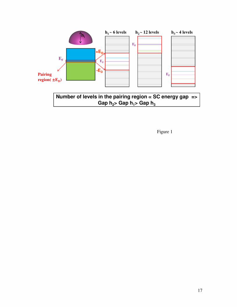
The origin of shell effects is primarily due to the discretization of the energy
levels in small particles which leads to substantial deviations of the superconducting
energy gap from the bulk limit. For small particles, the number of discrete energy levels
within a small energy window (pairing region) around the Fermi energy (EF) fluctuates
with very small changes in the system size. Consequently this leads to fluctuations in the
spectral density around EF. Since in weakly coupled superconductors electronic pairing
mainly occurs in a window of size ED (Debye energy) around EF, an increase (decrease)
of the spectral density around EF will make pairing more (less) favorable, thereby
increasing (decreasing) the energy gap (∆). As a consequence the gap becomes dependent

3
on the size and the shape of the particle (see schematic drawing in Fig. 1). The strength of
fluctuations also increases with the symmetry of the particle, since symmetry introduces
degeneracies in the energy spectrum. It is easy to see that these degenerate levels will
enhance the fluctuations in the spectral density and also in the gap as the number of levels
within ≤ΕD of EF, and consequently the number of electrons taking part in paring,
fluctuates dramatically. These degenerate levels will be referred to as ‘shells’ in analogy
with the electronic and nucleonic levels forming shells in atomic, cluster and nuclear
physics (see Ref. 3 and references therein). For cubic or spherical particles this might
lead to a large modification of ∆. Theoretically, these shell effects are described
quantitatively by introducing finite size corrections to the BCS model5,6
. In this letter,
through our scanning tunneling spectroscopic measurements on individual
superconducting nanoparticles of Pb and Sn, we demonstrate for the first time the
existence of these shell effects and the influence of the superconducting coherence length
on them.
Fig. 2a shows the schematic of the experimental measurement where an STM tip
is used to measure the tunneling density of states (DOS) of superconducting nanoparticles
of both Pb and Sn. A typical representative STM topographic image for Sn nanoparticles
(for Pb nanoparticle topographic image, see Ref. 17 ) with varying size on a BN/Rh(111)
substrate (see Methods for details) is shown in Fig. 2b. We take the height of the
nanoparticle as our reference since it is measured with a high degree of accuracy with the
STM. The quasiparticle excitation spectra (conductance plots of dI/dV vs V normalized at

4
+5mV) for a selection of Pb and Sn nanoparticles at a temperature of 1.2-1.4 K are
plotted in Figs. 2c-e. We fitted each spectrum with the tunneling equation,18
( ) ( ) ( ) ( ){ }
−−== ∫∞
∞−
dEeVEfEfENdV
dG
dV
dIVG snn
V
(1)
Where Ns(E) is the DOS of the superconductor, f(E) is the Fermi-Dirac distribution
function and Gnn is the conductance of the tunnel junction for V>>∆/e. Ns(E) is given by:
( )
∆−Γ+
Γ+=Γ
22)()(
)(Re),,(
TTiE
TiETENs
(2)
Where, ∆(Τ) is the superconducting energy gap and Γ(Τ) is a phenomenological
broadening parameter which incorporates all broadening arising from any non-thermal
sources (conventionally it is associated with the finite lifetime (τ) of the quasiparticles, Γ
~ ћ/τ)19
. There is an excellent agreement between the experimental data and the
theoretical fits, giving unique values of ∆ and Γ (plotted as a function of particle size in
Fig. 2f, g respectively). Comparing the raw data for the Pb and Sn, we observe that there
is a gradual decrease in the zero bias conductance dip with particle size for Pb
nanoparticles (Fig. 2c), while for Sn nanoparticles (Figs. 2d, e) there is a non monotonic
behavior which strongly depends on the particle size regime. We observe that though the
large Sn particles (>20 nm) differing in a size of 1 nm have similar DOS signifying
similar gaps, there is a large difference in the DOS and hence ∆, for the smaller Sn
particles (< 15 nm) even if they differ by less than 1 nm in size. The difference in the two
systems is brought out more clearly in Fig. 2f where we plot the normalized gap
(normalized with respect to their bulk values). For Pb, ∆ decreases monotonically with
decrease in particle size while there is a huge variation in the gap values for Sn below a

5
particle size of 20 nm. For these small sizes, gap values differ even more than 100% for
similar sized Sn particles and enhancements as large as 60% with respect to the Sn bulk
gap are found. In both systems however, superconductivity is destroyed below a critical
particle size which is consistent with the Anderson criterion,2
according to which
superconductivity should be completely destroyed for particle sizes where the mean level
spacing becomes equal to the bulk superconducting energy gap (see supplementary
information)20
. It is also worth noting that the average gap for the large Sn nanoparticles
(20-30 nm) shows an increase of 20% from the bulk value (See supplementary
information).
From the two parameters characterizing the superconducting state of our
nanoparticles, ∆ and Γ, only Γ evolves in a similar way as a function of particle size both
for Pb and Sn (Fig. 2g). In both systems, we observe an increase in Γ with reduction in
particle size. Interestingly, it seems that superconductivity is limited to sizes where Γ <
∆bulk.. At smaller sizes superconductivity is completely suppressed in both systems. This
indicates that Γ may have a particular significance in our measurements. To understand
the behaviour of Γ with particle size we invoke the role of quantum fluctuations in small
particles. It is known from both theoretical calculations and experiments that there should
be an increase in the quantum fluctuations in confined geometries21,22,23
as observed by
Bezryadin et al in their experiments on nanowires8. Similarly, since in a zero
dimensional superconductor the number of electrons taking part in superconductivity
decreases, we expect an increase in the uncertainty in the phase of the superconducting
order parameter18,19
(within a single particle, there will be a decrease in the long range

6
phase coherence). The increased fluctuations in the superconducting order parameter are
expected to increase Γ (as fluctuations act as a pair breaking effect). Therefore, we
associate Γ with the energy scale related with quantum fluctuations. Our results indicate
that in zero dimensional systems the presence of quantum fluctuations of the phase
(where Γ > ∆bulk) set the limit to superconductivity and this corresponds to the size
consistent with the Anderson criterion23
.
We focus now on the main result of this work, reflected in the variation of ∆ with
particle size in Sn nanoparticles, and the observed striking difference with Pb. In order to
interpret the experimental results we carry out a theoretical study of finite size corrections
in the BCS formalism in line with references 4, 5 and 6. We will primarily focus only on
the finite size corrections to the BCS gap equation since the corrections to the BCS mean
field approximation5 leads to a monotonic decrease in the gap
24 and are not responsible
for the observed oscillations in Sn nanoparticles. For the correction to the BCS gap
equation, two types of corrections are identified, smooth and fluctuating4,5
. The former
depends on the surface and volume of the grain and always enhances the gap with respect
to the bulk. Since this contribution decreases monotonically with the system size it is not
relevant in the description of the experimental fluctuations of ∆. In order to explain the
observed fluctuations of gap in Sn, we start with the self consistent equation for the BCS
order parameter5,6,
( ) ( ) ( )
( )'
)0(
)(
''2
','
22ε
ν
εν
εε
εεελε d
ID
D
E
E
∫− ∆+
∆=∆ (3)

7
where drrrVI
L
)()()',(2
'
0
2
εεεε ΨΨ= ∫ , ED is the Debye energy, L is a typical length of the
grain, ν(0) is the spectral density at the Fermi level, λ is the dimensionless coupling
constant, )()( i
i
ig εεδεν −=∑ where εi are the eigenvalues, with degeneracy gi, and ψε(r)
are the eigenfunctions with energy ε of a free particle confined inside the grain. For Sn, a
weak coupling superconductor a simple BCS formalism is capable of providing a good
quantitative description of superconductivity. Eqn. 3 can be further simplified by
noting4,5,6
that for kFL >> 1 gap oscillations are controlled only by ν(ε) . In our
experiment (where L ranges between 2-60 nm) we are always in this limit as the Fermi
wave vector kF = 16.4 nm-1
in Sn. As explained in the introduction, the gap oscillations
arise from the discreteness of the level spectrum (see Fig. 1) which is reflected in the
expression of the spectral density ν(ε) and hence Eqn. 3 leads to an oscillatory variation
of gap with particle size. It can also be seen from the expression of ν(ε) that the presence
of degenracies (gi > 1) will enhance the gap fluctuations. Large gi is typical of grains
with symmetry axes in which the energy levels are degenerate in a quantum number. A
typical example is the sphere with three axes of symmetry. In this case each level in the
energy spectrum with an angular momentum quantum number l is 2l+1 times degenerate.
We next proceed to solve Eqn. 3 numerically. Since we are only interested in
fluctuations, for simplicity in the calculations we will set I(ε,ε’) = 1. An important
parameter in Eqn. 3 is λ which implies an effective coupling constant (electron phonon
coupling minus the coulomb repulsion) providing strictly within the BCS formalism a
quantitative description of the superconductor. A natural choice is λ = 0.25 (for Sn) as

8
this leads to the bulk gap and the coherence length consistent with the experimental
values of these observables. The magnitude of the fluctuations will strongly depend on
the shape of the grain as expected from the theory of shell effects5. From the
experimental topographic images of the nanoparticles we can infer that the shape is very
close to being a hemisphere (It cannot be said with certainty since the diameter of the
particle is convoluted with the tip radius). However a statistical analysis of the
nanoparticle images reveals that the deviations from an ideal hemispherical shape should
not be larger than 15%. Hence for calculations, we model the shape of the nanoparticles
as being a spherical cap with h/R > 0.85. We solve Eqn. 3 numerically after computing
the εi for a given ratio of h/R. In the hemispherical case, h/R = 1, the eigenvalues are
simply the roots of a Bessel function. For other ratios, we use a method based on a
perturbative expansion around the hemispherical geometry which is only valid for 1 - h/R
<< 1 (similar to the treatment in Ref. 25). The parameters used to describe the Sn
nanoparticles are the height, h, measured by the STM, kF = 16.4 nm-1
, EF = 10.2 eV, ED =
9.5 meV and the coupling constant λ = 0.25. We plot the calculated normalized gap as
obtained from Eqn. 3 as a function of h (calculations done down till h = 10 nm to safely
remain within the validity of the BCS formalism) (solid lines in Fig. 3a) and superimpose
the experimental results of Sn nanoparticles from Fig. 2f (shown by solid symbols in Fig.
3a). Here the data is normalized with respect to the average gap value obtained
experimentally26
. For h/R ranging between 0.9 to 0.95 (see supplementary information)
we obtain a reasonably good quantitative matching with the theoretical results, indicating
that finite size corrections can satisfactorily explain the results of Sn nanoparticles.

9
The natural question which follows is why such oscillations in ∆ are not observed
for Pb nanoparticles (solid triangles in Fig. 2f) (Note that oscillations in the gap have
been observed in 2D Pb thin films below a critical thickness of 2 nm (thickness < Fermi
wavelength) as a function of the number of layers in the film (Ref. 11-13). This
phenomenon originates from the quantum confinement in the z direction leading to an
oscillatory behavior of the density of states at Fermi level (with infinite degeneracy of the
levels along the other two directions) and is independent of the superconducting
coherence length). We recall that fluctuations in 0D systems have its origin in the
discreteness of the spectrum and any mechanism that induces level broadening will
suppress these oscillations. The superconducting coherence length (ξ) of Pb (~80 nm)27
being much shorter than that of Sn (~240 nm)27
will introduce a level broadening
(broadening ∝ vF/ξ). Moreover, since interactions are much stronger in Pb, the lifetime of
the quasiparticles is shorter and an additional level broadening is expected. In Fig. 3b we
plot the average oscillations obtained from both experiments and theory as a function of
particle height for Pb and Sn nanoparticles. These average oscillations are the standard
deviation of the gap from the average value26
. We observe a good matching between
theory and experiments. We would like to point out that for Pb the BCS description is an
oversimplified model and one needs to solve the Eliashberg equations28
to obtain the
correct average gap values. However, to compute the oscillations in the gap and to check
the suppression of the shell effects, BCS gives a reasonably good description for the
strong coupling Pb (Fig. 3b).

10
Our results indicate that for any classical BCS superconductor with large quantum
coherence lengths it is possible to enhance the superconducting energy gap by large
factors (~60%) by tuning only the particle size. This may prove to be very useful in case
of fullerides or hexaborides which are known to show a relatively high Tc in the bulk.
Methods:
The experiments were performed in an ultra high vacuum (UHV) system (base pressure <
5x10-11
Torr) combined with a home-built low temperature STM. The base temperature
was 0.9 K. Differential conductance (dI/dV) spectra were measured with a tungsten (W)
tip with open feedback loop using the lock-in technique with a 50 µV voltage
modulation. A stabilization current of 0.1 nA and an initial sample voltage of 8.0 mV was
used to measure all the tunneling spectra. The Pb and Sn nanoparticles of 1-35 nm height
were grown in situ on top of a BN/Rh(111) surface by means of buffer layer assisted
growth29
(see Fig. 2b) where the BN having a band gap of ~6 eV acts as a decoupling
layer. The topographic images of the nanoparticles on the surface were taken with the
STM. The 3D plots were obtained by using the WSxM software.30
References:
1 Von Delft, J. Superconductivity in ultrasmall metallic grains. Annalen der Physik 10,
219-276 (2001).
2 Anderson, P. W. Theory of dirty superconductors. J. of Phys. and Chem. of Solids 11,
26-30 (1959).

11
3 Kresin, V. Z. & Ovchinnikov, Y. N. Shell structure and strengthening of
superconducting pair correlation in nanoclusters. Phys. Rev. B 74, 024514-11 (2006).
4 Heiselberg, H. Pairing of fermions in atomic traps and nuclei. Phys. Rev. A 68, 053616-
10 (2003).
5 Garcia-Garcia, A. M., Urbina, J. D., Yuzbashyan, E. A., Richter, K. & Altshuler, B. L.
Bardeen-Cooper-Schrieffer Theory of Finite-Size Superconducting Metallic Grains.
Phys. Rev. Lett. 100, 187001-4 (2008).
6 Olofsson, H., Aberg, S. & Leboeuf, P. Semiclassical Theory of Bardeen-Cooper-
Schieffer Pairing-Gap fluctuations. Phys. Rev. Lett, 100, 037005-4 (2008).
7 Ralph, D. C., Black, C. T. & Tinkham, M. Spectroscopic Measurements of Discrete
Electronic States in Single Metal Particles. Phys. Rev. Lett. 74, 3241-3244 (1995).
8 Bezryadin, A., Lau, C. N. & Tinkham, M. Quantum suppression of superconductivity in
ultrathin nanowires. Nature 404, 971-974 (2000).
9 Shanenko, A. A., Croitoru, M. D., Zgirski, M., Peeters, F. M. & Arutyunov, K. Size-
dependent enhancement of superconductivity in Al and Sn nanowires: Shape-resonance
effect. Phys. Rev. B 74, 052502-4 (2006).
10 Qin, S., Kim, J., Niu, Q. & Shih, C.-K. Superconductivity at the Two-Dimensional
Limit. Science 324, 1314-1317 (2009).
11 Guo, Y. et al. Superconductivity Modulated by Quantum Size Effects. Science 306,
1915-1917 (2004).
12 Zhang, F-Y. et al, Band Structure and Oscillatory Electron-Phonon Coupling of Pb
Thin Films Determined by Atomic-Layer-Resolved Quantum-Well States. Phys. Rev.
Lett. 95, 096802-4 (2005).

12
13
Shanenko, A. A., Croitoru, M. D. & Peeters, F. M. Quantum size effects on Tc of
superconducting nanofilms. Europhys. Lett. 76, 498-504 (2006).
14 Brun, C. et al,. Reduction of the Superconducting Gap of Ultrathin Pb Islands Grown
on Si(111). Phys. Rev. Lett. 102, 207002-4 (2009).
15 Bose, S., Raychaudhuri, P., Banerjee, R., Vasa, P. & Ayyub, P. Mechanism of the Size
Dependence of the Superconducting Transition of Nanostructured Nb. Phys. Rev. Lett.
95, 147003-4 (2005).
16 Li, W. H. et al. Coexistence of ferromagnetism and superconductivity in Sn
nanoparticles. Phys. Rev. B 77, 094508-7 (2008).
17 Brihuega, I. et al, Quantum and critical fluctuations in the superconductivity of single,
isolated Pb nanoparticles. arXiv:0904.0354v1 (2009).
18 Tinkham, M. Introduction of Superconductivity, 2nd edition (McGraw Hill, Singapore,
1996).
19 Dynes, R. C., Narayanamurti, V. & Garno, J. P. Direct Measurement of Quasiparticle-
Lifetime Broadening in a Strong-Coupled Superconductor. Phys. Rev. Lett. 41, 1509-
1512 (1978). This equation is phenomenological though it works in many different
systems.
20 In recent years this criteria has been substantially refined where it is accepted that
superconductivity is destroyed at sizes depending on the parity of the grain and can be
lower than that predicted by the Andersons criterion. See, Delft, V-J., Zaikin, A.D.,
Golubev, A. S. & Tichy, W. Parity-affected superconductivity in ultrasmall metallic
grains, Phys. Rev. Lett. 77, 3189-3192 (1996). We think that we are not sensitive to the
parity of the particle.

13
21 Dynes, R. C., Garno, J. P., Hertel, G. B. & Orlando, T. P. Tunneling Study of
Superconductivity near the Metal-Insulator Transition. Phys. Rev. Lett. 53, 2437-2440
(1984).
22 Skocpol, W. J. & Tinkham, M. Fluctuations near superconducting phase transitions.
Rep. on Prog. in Phys., 1049-1097 (1975).
23 Bennemann, K. H. & Ketterson, J. B. Superconductivity:Conventional and
Unconventional Superconductors, Volume 1 (Springer, 2008).
24 The leading correction to the BCS prediction is given by ∆ = ∆BCS – δ/2 where ∆BCS is
the bulk gap and δ is the discrete energy level spacing of the nanoparticle. This predicts a
decrease in the average gap with reduction in particle size and can qualitatively explain
the monotonic dependence of the average gap in both Pb and Sn nanoparticles.
25 Rodríguez, A. H., Trallero-Giner, C., Ulloa, S. E. & Marín-Antuña, J. Electronic states
in a quantum lens, Phys. Rev. B 63, 125319-9 (2001).
26 We divided the particle size in small bins of 2 nm wide and the average of the
superconducting energy gap in each bin was determined.
27 Kittel, C. Introduction to Solid State Physics, 8th edition (Wiley, 2004).
28 Bergmann, G. & Rainer, D. The sensitivity of the transition temperature to changes in
α2F(ω). Z. Phys, 263, 59-68 (1973).
29 Berner, S. et al. Boron Nitride Nanomesh: Functionality from a Corrugated Monolayer.
Angew. Chem. Int. Ed. 46, 5115-5119 (2007).
30 Horcas, I. et al. WSXM: A software for scanning probe microscopy and a tool for
nanotechnology. Rev. of Sci. Inst. 78, 013705-8 (2007).

14
Acknowledgements
We will like to thank Prof. K. Richter and Dr. M. Ternes for critically reading the
manuscript. S.B. would like to thank the Alexander von Humboldt foundation and I. B.
the Marie Curie action for support. A. M. G. G acknowledges financial support from the
Spanish DGI through project No. FIS2007-62238.
Author contributions
S.B., I.B. and K.K. designed the research. S.B. and I.B. performed the experiments
supervised by K.K.. A.M.G.G and J.D.U. provided the theoretical support. M.M.U and
C.H.M helped in the experiments. S.B. and I.B. analyzed the data. The paper was written
by S.B. and A.M.G.G. All authors contributed to the scientific discussion and revised the
manuscript.
Additional information
The authors declare no competing financial interests. Correspondence and requests for
materials should be addressed to S.B, I. B and A. M. G. G.
Figure Captions:
Figure 1 | Schematic of Shell effects
Schematic explaining the physical origin of shell effects in small particles which leads to
an oscillation in the gap value with particle size. The left panel shows the energy band
diagram of a small particle with a height h where the discretization of the energy levels is
arising from quantum confinement. Also for a particle with definite axes of symmetry,

15
each level has further degeneracies and each degenerate level in a small particle is
referred to as the ‘SHELL’. Now, in superconductivity only the levels within the pairing
region (Debye window) about the Fermi level, EF takes part in pairing and consequently
superconductivity. We show the expansion of this pairing region for three particles with
heights h1, h2 and h3 which are very close to each other (so that the mean level spacing is
quite similar). The number of levels in this pairing window fluctuates depending on the
position of the Fermi level in the three particles which leads to the fluctuation in the gap
(Shell effects).
Figure 2 | Experimental configuration and low temperature superconducting
properties of single, isolated Pb and Sn nanoparticles: Observation of Shell effects
a, 3D representation of the experimental set-up. Superconducting nanoparticles deposited
on a BN/Rh(111) substrate vary in height between 1-35 nm and are probed individually
with the help of the STM tip.
b, 125 X 90 nm2 3D STM image showing the Sn nanoparticles of varying sizes deposited
on the BN/Rh (111) substrate. The scale bar is shown in the left. The image is taken at a
sample bias voltage of 1 V with a tunneling current of It = 0.1 nA. This is a representative
of topographic images of the superconducting Pb and Sn nanoparticles on the substrate.
c-e, Normalized conductance spectra (dI/dV vs V, normalized at a bias voltage of 5 mV).
The circles are the raw experimental data and the solid lines are the theoretical fits using
Eqns. 1 and 2 (see text). c, for Pb nanoparticles of different heights at T = 1.2 K. d, for
two large Sn nanoparticles with heights 29.5 and 29.0 nm at T = 1.4 K. e, for two small
Sn nanoparticles with heights 10.5 and 10.0 nm at T = 1.4 K.

16
f,g Comparison of the variation of superconducting energy gap (∆) and broadening
parameter (Γ) at low temperature (T = 1.2 K-1.4 K) for different Pb and Sn nanoparticles
respectively as a function of particle height. The gap is normalized with respect to the
bulk gaps. Observation of Shell effects in Sn nanoparticles. The solid lines in f are guides
to the eye.
Figure 3 | Comparison of experimental results with theoretical calculations obtained
from finite size corrections to the BCS model.
a, Variation of normalized gap with particle height. The solid symbols are obtained from
the experimental data and the solid line is obtained from the theoretical calculations. The
oscillations in the gap are explained on the basis of shell effects obtained from finite size
corrections to the BCS model.
b, Variation in the average oscillations in the gap for Pb and Sn with particle height. The
solid symbols are experimental data while the dashed lines are obtained from the
theoretical calculations.
17
hi
Number of levels in the pairing region ∝ SC energy gap =>
Gap h2> Gap h1> Gap h3
EF
Pairing
region( ±ED)
h1 ~ 6 levels h2 ~ 12 levels h3 ~ 4 levels
EF
EF
EF
+ED
-ED
Figure 1

18
a b
0 nm
11 nm
0 5 10 15 20 25 300.0
0.4
0.8
1.2
1.6
Sn nanoparticles
Pb nanoparticles
∆/∆
bulk
Particle Height (nm)
f
-4 -2 0 2 4
0.5
1.0
1.5
30 nm 16.5 nm
13 nm
8.3 nm 5 nm
4.4 nm
BN substrate
dI/d
V (
arb
. u
nits)
Bias Voltage (mV)
c
T = 1.2 K
Pb nanoparticles
-4 -2 0 2 4
0.5
1.0
1.5
10.5 nm, ∆ = 0.50meV
10.0 nm, ∆ = 0.89 meV
dI/
dV
(arb
. units)
Bias Voltage (mV)
T = 1.4 K
e Small Sn nanoparticles
-4 -2 0 2 4
0.5
1.0
1.5
29.5 nm, ∆ = 0.71 meV
29.0 nm, ∆ = 0.70 meV
dI/
dV
(arb
. units)
Bias Voltage (mV)
T = 1.4 K
d Large Sn nanoparticles
BN
STM tip
Pb or Sn nano-particle
Rh(111)
VI
BN
STM tip
Pb or Sn nano-particle
Rh(111)
VI
0 5 10 15 20 25 300.0
0.4
0.8
1.2 Pb nanoparticles
Sn nanoparticles
∆bulk
for Sn = 0.57 meV
g
Γ (
me
V)
Particle Height (nm)
∆bulk
for Pb = 1.36 meV
Figure 2

19
10 15 20 25 300
10
20
Sn nanoparticles
Pb nanoparticles
Theory (h = 0.9R)
Averg
ae
oscill
atio
ns
in g
ap (
%)
Particle Height (nm)
b
10 15 20 25 300.0
0.5
1.0
1.5
2.0
No
rmaliz
ed G
ap
Particle Height (nm)
Theory
Expt. data
h = 0.9Ra
Figure 3