Nonlinear Optical Studies of Defects and Domain Structures in ...
186
City University of New York (CUNY) City University of New York (CUNY) CUNY Academic Works CUNY Academic Works Dissertations, Theses, and Capstone Projects CUNY Graduate Center 9-2017 Nonlinear Optical Studies of Defects and Domain Structures in Nonlinear Optical Studies of Defects and Domain Structures in Perovskite-Type Dielectric Ceramics Perovskite-Type Dielectric Ceramics David J. Ascienzo The Graduate Center, City University of New York How does access to this work benefit you? Let us know! More information about this work at: https://academicworks.cuny.edu/gc_etds/2315 Discover additional works at: https://academicworks.cuny.edu This work is made publicly available by the City University of New York (CUNY). Contact: [email protected]
-
Upload
khangminh22 -
Category
Documents
-
view
2 -
download
0
Transcript of Nonlinear Optical Studies of Defects and Domain Structures in ...
City University of New York (CUNY) City University of New York (CUNY)
CUNY Academic Works CUNY Academic Works
Dissertations, Theses, and Capstone Projects CUNY Graduate Center
9-2017
Nonlinear Optical Studies of Defects and Domain Structures in Nonlinear Optical Studies of Defects and Domain Structures in
Perovskite-Type Dielectric Ceramics Perovskite-Type Dielectric Ceramics
David J. Ascienzo The Graduate Center, City University of New York
How does access to this work benefit you? Let us know!
More information about this work at: https://academicworks.cuny.edu/gc_etds/2315
Discover additional works at: https://academicworks.cuny.edu
This work is made publicly available by the City University of New York (CUNY). Contact: [email protected]
NONLINEAR OPTICAL STUDIES OF DEFECTS AND
DOMAIN STRUCTURES IN PEROVSKITE-TYPE DIELECTRIC CERAMICS
by
DAVID J. ASCIENZO
A dissertation submitted to the Graduate Faculty in Physics in partial fulfillment of the
requirements for the degree of Doctor of Philosophy, The City University of New York
2017

ii
© 2017
DAVID J. ASCIENZO
All Rights Reserved
iii
Nonlinear Optical Studies of Defects and Domain Structures in Perovskite-type Dielectric Ceramics
by
David J. Ascienzo
This manuscript has been read and accepted by the Graduate Faculty of Physics in satisfaction of the dissertation requirement for the degree of Doctor of Philosophy.
Date Professor Yuhang Ren
(Chair of Examining Committee)
Date Professor Igor L. Kuskovsky
(Executive Officer)
Supervisory Committee:
Professor Steven Greenbaum
Professor Ying-Chih Chen
Professor Jun Ouyang
Professor Yu Zhang
THE CITY UNIVERSITY OF NEW YORK

iv
Abstract
Nonlinear Optical Studies of Defects
and Domain Structures in Perovskite-type Dielectric Ceramics
by
David J. Ascienzo
In order to improve future generations of ceramic capacitors, a deeper understanding of
voltage-induced dielectric breakdown and electrical energy storage limitations in these materials
is required. This dissertation presents the use of far-field optical second harmonic generation
(SHG) polarimetry, as well as photoluminescence and confocal Raman spectroscopy, for
investigating: 1) dc electric field-induced structural distortions at undegraded Fe-doped SrTiO3
(Fe:STO) electrode interfaces, 2) structural defect and strain formation due to oxygen vacancy
migration in electrodegraded Fe:STO single crystals, and 3) mixed tetragonal and rhombohedral
phases in ferroelectric Zr-doped BaTiO3 (BZT) thick films exhibiting high energy densities and
efficiencies.
First, electric field-induced second harmonic generation (EFISHG) and photoluminescence
spectroscopy were used to study local structural changes at electrode interfaces in reduced and
oxidized Fe:STO single crystals at room temperature. Results show that ionic displacements along
the applied field axis lead to electrostrictive distortions which are described by Fe:Ti-O bond
stretching and bending effects in Fe:Ti-O6 octahedra. Differences in the EFISHG responses of the
oxidized and reduced crystals are explained by the Schottky barriers and built-in electric fields at
their metal-dielectric interfaces which depend strongly on local oxygen vacancy concentrations.

v
The built-in electric field in the interfacial depletion region is revealed to be greater in oxidized
Fe:STO compared to reduced Fe:STO, leading to stronger structural changes at low dc voltages in
the reduced crystal compared to the oxidized one. Structural differences between the reduced and
oxidized Fe:STO cathodes are indicated by both EFISHG and photoluminescence measurements,
showing that the clustering of oxygen vacancies at the reduced cathode leads to deviations from
tetragonal (4mm) symmetry.
Second, structural defect and strain formation in electrodegraded reduced and oxidized
Fe:STO single crystals were investigated using optical SHG and confocal Raman measurements.
SHG revealed structural inhomogeneity resulting from the formation of Fe4+/oxygen ion and
Fe3+/oxygen vacancy aggregation sites along the degraded anode and cathode interfaces,
respectively. It is also shown that mixed Fe3+/Fe4+ states and strain are generated across the
electrocoloration boundaries, or color fronts, in both crystals. These results, as well as oxygen
sublattice variations between the anodic and cathodic bulk shown by confocal Raman data, depict
the creation of a structural interface along the color front. In comparing both electrodegraded
oxidized and reduced Fe:STO crystals, we reveal that structural strain is higher across the oxidized
crystal’s color front compared to the reduced crystal, although this strained region is slightly wider
in the reduced crystal compared to the oxidized one. We further indicate that structural and
electrochemical inhomogeneity has a dependence on the distance between electrodes due to the
finite size of the strained region across both color fronts.
Third, optical SHG polarimetry was used in the reflection and transmission geometries to
characterize heterophase polydomain structures in Zr-doped BaTiO3 (BZT) ferroelectric films
exhibiting high energy storage densities and efficiencies. Under a compressive film-substrate
misfit strain, tetragonal and rhombohedral phases can coexist in these films as elastic domains. In

vi
the reflection geometry, the SHG signal arises primarily from compressive strain-induced
tetragonal domains growing along the thickness of the film. In the transmission geometry, the SHG
signal arises from rhombohedral domains and the SHG contributions from tetragonal domains
effectively vanishes. Rhombohedral symmetry is shown to increase with film thickness as a result
of strain relaxation away from the tetragonal film-substrate interface. Greater misfit strains are
shown to lead to a higher degree of tetragonal symmetry in the films. In addition, the presence of
mixed rhombohedral and tetragonal phases is supported by transmission electron microscopy
(TEM) and x-ray diffraction (XRD) measurements. The high energy performance of the films is
directly connected to these mixed tetragonal and rhombohedral polydomain structures which serve
to decrease remnant polarizations and help delay saturation of the dielectric’s polarization.

vii
Acknowledgements
First of all, I would like to thank my advisor, Prof. Yuhang Ren, whose constant support
and feedback were an invaluable part of my journey. I will never forget the time and energy he
spent mentoring me. I would also like to thank Prof. Steve Greenbaum, Prof. Ying-Chih Chen, Dr.
Jun Ouyang, and Prof. Yu Zhang for participating in my supervisory committee.
I’d like to thank the physics faculty at Hunter College for all their hard work. Special thanks
to Prof. Rodney Varley, Prof. Hyungsik Lim, Prof. Godfrey Gumbs, Prof. Leon Cohen, Prof.
Neepa Maitra, and Prof. Marilyn Rothschild. All of you helped me forge a passion for physics
which I will continue to nurture for years to come.
I’d like to thank the faculty members at the CUNY Graduate Center who took time out of
their research schedules to lecture not only for me, but for all of the graduate students invested in
higher education. I would especially like to thank Prof. Tobias Schafer (Mathematical Methods),
Prof. Timothy Boyer (Electromagnetic Theory), Prof. Giovanni Ossola (Quantum Mechanics),
Prof. Nicolas Giovambattista (Statistical Mechanics), Prof. Sharon Loverde (Computational
Methods), Prof. Hernan Makse (Complex Networks), and the very supportive and knowledgeable
Geva Patz (Big Data Analysis). A special thanks goes out to Daniel Moy and Renee Sasaki for
guiding me through the bureaucratic intricacies of the program.
I’d like to thank my father, sister, and mother for believing in me and putting up with my
mysterious disappearances and radio silence. I would also like to thank the fantastical Sadlier and
Immendorf family for their overflowing support and holiday parties.

viii
I would also like to express gratitude to my friends and colleagues for their support. A lot
of special thanks goes out to Devon Boscio, Jon Cronin, Dan Koch, Dov Fields, Stephen Munoz,
Onur Kurt, Gong Yu, Zehra Cevher, Haochen Yuan, Dr. Ying, Tony Le, Max Hyland, Melissa
Kenny, Courtney and Chris Foxz, Maryn Schieber, Caelyn Mecca, Aaron Williams and of course
the Kenny family!
Lastly, but most importantly, I would like to thank my partner, Jaclyn Sadlier, for being
there for me every single arduous step of the way! Everything from getting up in the morning to
writing this dissertation was made easier by your constant care and love. Thank you so much for
going above and beyond to ensure that my head didn’t fall off. Without you, I don’t think any of
this would have been possible. I love you!

ix
Table of Contents
Abstract ......................................................................................................................................... iv Acknowledgements ..................................................................................................................... vii Table of Contents ......................................................................................................................... ix List of Tables ............................................................................................................................... xii List of Figures ............................................................................................................................. xiii
Chapter 1: Introduction and Motivation .....................................................................................1
1.1 dc Electric Field-induced Degradation in Perovskite-type Dielectrics ................................2
1.2 Strain Field-tuning of Perovskite-type Ferroelectric Films .................................................9
1.3 Scope of Dissertation .........................................................................................................14
Chapter 2: Theoretical Background .........................................................................................16 2.1 Structure and Dielectric Properties ....................................................................................16
2.1.1 Perovskite-type Ceramics ......................................................................................20
2.2 Defect Chemistry in Fe:STO .............................................................................................22
2.2.1 Structural Defects ...................................................................................................27
2.3 Resistance Degradation in Fe:STO ....................................................................................29
2.3.1 Reduction Model ....................................................................................................29
2.3.2 Electrocoloration ....................................................................................................29
2.3.3 Electrostriction .......................................................................................................29
2.3.4 Metal-dielectric Interface .......................................................................................31
2.4 Domain Structures in BZT Films .......................................................................................33
2.4.1 Heterophase Polydomain Structures ......................................................................35
2.4.2 Strain-field Tuning of Domain Structures .............................................................36
2.5 Optical Second Harmonic Generation ...............................................................................38
2.5.1 Nonlinear Electron Spring Model ..........................................................................40
2.5.2 Tensor Representation of the Second-Order Susceptibility ...................................48

x
2.5.3 SHG Phase Matching .............................................................................................52
Chapter 3: Experimental Details ................................................................................................55 3.1 Samples .............................................................................................................................55
3.1.1 Fe:STO Single Crystals .........................................................................................55
3.1.2 BZT Films ..............................................................................................................59
3.2 Femtosecond Laser Systems ..............................................................................................61
3.2.1 Mode-locked Ti:Sapphire Oscillator ......................................................................61
3.2.2 Ti:Sapphire Regenerative Amplifier ......................................................................68
3.3 Optical SHG Polarimetry ...................................................................................................70
3.4 Confocal Raman Spectroscopy ..........................................................................................77
3.5 Photoluminescence Spectroscopy ......................................................................................78
Chapter 4: Local Structural Changes due to the Electric Field-Induced Migration of Oxygen Vacancies at Fe-doped SrTiO3 Interfaces ...................................................................81 4.1 dc Electric Field-induced SHG from Fe:STO Interfaces ..................................................81
4.1.1 Experimental and Theoretical Description ............................................................81
4.1.2 EFISHG from Anode and Cathode Interfaces .......................................................89
4.2 Photoluminescence from Fe:STO Interfaces .....................................................................95
4.3 Schottky Junctions at Pt-Fe:STO Interfaces ......................................................................98
4.4 Summary .........................................................................................................................102
Chapter 5: Formation of Structural Defects and Strain in Electrodegraded Fe-doped SrTiO3 Single Crystals due to Oxygen Vacancy Migration ..................................................104
5.1 Optical SHG from Electrodegraded Fe:STO Single Crystals ..........................................104
5.1.1 Experimental and Theoretical Description ..........................................................104
5.1.2 SHG from Electrodegraded Interfaces .................................................................110
5.1.3 SHG from Electrocolored Bulks ..........................................................................114
5.2 Confocal Raman from Electrocolored Fe:STO Bulks ....................................................118
5.3 Oxygen Vacancy Migration-induced Structural Changes ..............................................121

xi
5.4 Summary .........................................................................................................................124
Chapter 6: Detection of Coexisting Tetragonal and Rhombohedral Phases in Ferroelectric Zr-doped BaTiO3 Thick Films using Second Harmonic Generation ....................................126 6.1 Optical SHG from BZT Thick Films ..............................................................................126
6.1.1 Experimental and Theoretical Description ..........................................................126
6.1.2 SHG in Reflection Geometry from BZT Films ...................................................129
6.1.3 SHG in Transmission Geometry from BZT Films ..............................................134
6.2 XRD and TEM Results from BZT Films .........................................................................138
6.3 High Energy Performance due to the Formation of Heterophase Polydomain Structures ..........................................................................................................................................141
6.4 Summary .........................................................................................................................143
Chapter 7: Summary and Outlook ...........................................................................................144
7.1 General Summary ...........................................................................................................144
7.2 Outlook and Future Experiments ....................................................................................146
Bibliography ...............................................................................................................................148

xii
List of Tables
Table 3.1: Defect concentrations for the initial, undegraded Fe:STO states at the annealing (900
°C), quenching (25 °C), and investigation (25 °C) conditions. .....................................................55
Table 3.2: Ferroelectric BZT film samples listed with their respective thicknesses, substrates, and
substrate lattice parameters at room temperature. ..........................................................................59
Table 5.1: Extrapolated nonlinear susceptibility components from SHG intensity fittings for the
electrodegraded Fe:STO anode and cathode interfaces....................................................................110
xiii
List of Figures
Figure 1.1: Illustration of oxygen vacancy migration in a typical parallel-plate, metal-dielectric-
metal, capacitor. The initially uniform distribution of oxygen vacancies changes in response to the
dc electric field. ................................................................................................................................4
Figure 1.2: Comparison between a non-polar (cubic SrTiO3) perovskite unit cell and a polar
(tetragonal BaTiO3) perovskite unit cell (Graphic made in Avogadro 1.1.1). ...............................11
Figure 1.3: Polarization-electric field (P-E) hysteresis loops, as shown by Cheng et al. (a) Typical
ferroelectric hysteresis loop; (b) Example of a slim hysteresis loop; (c) Partially shown hysteresis
curves near their respective saturation points. Delayed saturation results in a higher energy density.
For all figures, the green area represents the discharged energy density (𝑊"), while the brown area
is the energy loss (𝑊#$%%). ..............................................................................................................11
Figure 2.1: Examples of polar domain variants in ferroelectric materials exhibiting tetragonal
(4mm) and rhombohedral (3m) symmetry. On the left a centrosymmetric cubic unit cell is shown
for reference. In the middle, a non-centrosymmetric tetragonal unit cell is shown where the solid
arrow points in the direction of the 100 polarization and dashed arrows point in other 5 possible
directions. On the right, a non-centrosymmetric rhombohedral unit cell is shown where the solid
arrow points in the direction of the 111 polarization and dashed arrows point in the other 7
possible directions. .........................................................................................................................19

xiv
Figure 2.2: Depiction of a typical perovskite lattice composition using SrTiO3. Four Sr cations
(green A-sites) sit at the corners of the cubic unit cell, six oxygen anions sit (red O-sites) at the
corners of a central octahedron, and a central titanium cation (grey B-site) sits inside the oxygen
octahedron. .....................................................................................................................................19
Figure 2.3: Examples of various perovskite-type ceramics and their multiple functions. ...........21
Figure 2.4: Fe:Ti-O6 octahedral centers found throughout the Fe:STO crystal lattice. (a) Cubic
Ti4+ center (uncharged). (b) Tetragonal Fe3+ defect center (-1 charge). (c) Jahn-Teller distortion of
the Fe4+ defect center (uncharged). (d) Oxygen vacancy formation near an Fe3+ defect center (+1
charge). Fe-defect centers (b), (c), and (d) portray tetragonal (4mm) symmetry. Dashed black
arrows show the stretching or compression of crystal physics axes, a and c. ..............................27
Figure 2.5: Electronic distribution at a metal-dielectric interface, approximated using Eq. 2.18.
The light grey shaded region represents the metal electrode, while the white region represents the
dielectric. The red solid curve signifies the electronic density across the junction. ......................32
Figure 2.6: Plot shown from Cheng et al. Equilibrium phase of Ba(ZrxTi1-x)O3 as a function of Zr-
doping with (Dashed line) and without (Solid line) compressive strain. The room temperature
equilibrium bulk phase transforms from tetragonal (4mm) in undoped BTO to rhombohedral (3m)
in 20% Zr-doped BTO (BaZr0.2Ti0.8O3). ........................................................................................34
xv
Figure 2.7: Shows different misfit strains which can form between the epitaxial ferroelectric film
and the tetragonal substrate. (a) The case where 𝑎) = 𝑎% doesn’t result in a misfit strain; (b) The
case where 𝑎) > 𝑎% leads to a compressive strain on the film; (c) The case where 𝑎) < 𝑎% leads to
an expansive tensile strain on the film. Short-dashed lines mark the interface sites for clarity. ..37
Figure 2.8: Energy diagram for optical second harmonic generation. Two photons of energy E =
ℏ𝜔 are absorbed, exciting the system to a virtual state. Then, one photon of energy E = 2ℏ𝜔 is
emitted as the system returns to its ground state.................................................................................39
Figure 2.9: Illustration of an electric field polarizing the electron cloud around an atom. The
interaction can be modeled as an effective charge attached to a spring where 𝐹0 and 𝐹1 are the
restoring force of the spring and Lorentz force, respectively. .......................................................41
Figure 2.10: Linear optical susceptibility as a function of frequency. The dispersion function is
represented by the real part (solid red line) and the resonance function is represented by the
imaginary part (dashed black line). Curves are rescaled for convenience. ....................................44
Figure 2.11: Nonlinear optical susceptibility as a function of frequency. The dispersion function
is represented by the real part (solid red line) and the resonance function is represented by the
imaginary part (dashed black line). Curves and axes are rescaled for convenience. .....................47
xvi
Figure 2.12: Shows the sinc functional term plotted as a function of distance from the surface of
the nonlinear material. Considering light propagation in the positive direction, the SHG coherence
length is given by the two vertical red lines, with the second line marking the start of destructive
interference. Complete destructive interference occurs at twice the coherence length, as shown by
the first minima. .............................................................................................................................53
Figure 3.1: XRD measurements taken from Fe:STO with and without the 10 nm Pt electrodes to
show that the structure of the platinum electrodes is amorphous. ................................................57
Figure 3.2: Planar and lateral platinum electrode placement for dc electric field application across
Fe:STO single crystals. ..................................................................................................................58
Figure 3.3: (a) Current density measurements taken from the electrodegraded Fe:STO single
crystals with planar electrodes, B042 and B045. (b) Current density measurements taken from the
electrodegraded Fe:STO single crystals with lateral electrodes, B056 and B057. ........................58
Figure 3.4: Shows the typical sequential structure for the ferroelectric thick films studied in this
work. Circular Au electrodes are spread across the BZT surface. Beneath the bulk layers of the
BZT film lies the SRO electrode layer over the surface of the perovskite oxide substrate. .........58
Figure 3.5: Schematic for the mode-locked Ti:Sapphire oscillator (Tsunami, Spectra-physics).
........................................................................................................................................................62

xvii
Figure 3.6: The first nine longitudinal modes inside the optical cavity. .......................................65
Figure 3.7: (a) Cumulative electric field in the cavity calculated from summing the first 30
longitudinal modes. The electric field is shown propagating left to right over time. (b) Pulse
intensity traveling to the right. A pulse leaves the output coupler each cycle. ..............................66
Figure 3.8: Spectral distribution of the pulsed laser output measured with an optical spectrum
analyzer (Newport OSM-100-VIS/NIR). In our experiments, we tune the central wavelength to
810 nm and the bandwidth (FWHM) to 10 nm. .............................................................................68
Figure 3.9: A schematic of the Ti:Sapphire regenerative amplifier system (RegA 9000, Coherent).
........................................................................................................................................................69
Figure 3.10: Generalized diagram for optical SHG experiments in our lab. Laser pulses emitted
from either the RegA 9000 or Tsunami are passed through a mechanical chopper and enter the
detection setup configured for generating polarization-resolved SHG signals. The induced SHG
signal is then directed into a photomultiplier tube (PMT) and the lock-in amplified signal is
recorded through a LabVIEW program. ........................................................................................70
Figure 3.11: Schematics for far-field optical SHG polarimetry setups in the (a) transmission
geometry and (b) reflection geometry. ...........................................................................................70

xviii
Figure 3.12: Refractive index for STO and BTO plotted as functions of the optical wavelength in
micrometers. Index of refraction values for 810 nm and 405 nm light are given in the upper right-
hand corners of each subplot. .........................................................................................................75
Figure 3.13: Experimental configuration for confocal Raman spectroscopy in the reflection
geometry. Laser light is focused onto the sample and Raman scattered light is directed into a
spectrograph using focusing lenses. ...............................................................................................78
Figure 3.14: Experimental configuration for photoluminescence spectroscopy in the front-face
detection geometry. Light from the Xenon lamp is filtered by an excitation monochromator which
allows single wavelengths of light to reach the sample. The sample emits fluorescence in response
to the incoming radiation which is filtered by an emission monochromator that feeds the signal
into a PMT coupled to a photon counter. .......................................................................................79
Figure 4.1: (a) Schematic for optical SHG in the reflection geometry. Focusing lenses are marked
by L1, L2, and L3. A band-pass filter (BPF) is used to block fundamental light from entering the
PMT. A long-pass filter (LPF) is placed before the sample to filter out residual SHG light from the
laser system. A half-wave plate (𝜆/2) is used to rotate the polarization axis of the incident
fundamental light. The insert shows the configuration with a dc-bias; (b) Schematic of the incident
and outgoing light path and polarization for SHG measurements in the reflection geometry. (x, y,
z) define the laboratory coordinates and [100], [010], and [001] define crystal axes. Incident and
outgoing pulses travel along the xz-plane at an angle 𝜃6 with respect to the surface normal. 𝑒(𝜔)
xix
and 𝑒(2𝜔) are polarization unit vectors for incident and outgoing light. Here, p- and s-polarized
optical fields travel parallel and perpendicular to the xz-plane, respectively. ...............................83
Figure 4.2: Optical SHG measurements taken from the reduced Fe:STO crystal. (a) p-polarized
and (b) s-polarized EFISHG intensities plotted as functions of the incident light polarization angle
for positive dc voltages (anode interface). (c) p-polarized and (d) s-polarized EFISHG intensities
plotted as functions of the incident light polarization angle for negative dc voltages (cathode
interface). ......................................................................................................................................89
Figure 4.3: Optical SHG measurements taken from the oxidized Fe:STO crystal. (a) p-polarized
and (b) s-polarized EFISHG intensities plotted as functions of the incident light polarization angle
for positive dc voltages (anode interface). (c) p-polarized and (d) s-polarized EFISHG intensities
plotted as functions of the incident light polarization angle for negative dc voltages (cathode
interface). .......................................................................................................................................91
Figure 4.4: EFISHG intensities and susceptibilities as functions of the imposed voltage. EFISHG
intensities plotted as functions of the imposed dc voltage for the (a) reduced Fe:STO and (b)
oxidized Fe:STO single crystals. Effective susceptibilities plotted as functions of the imposed dc
voltage for the (c) reduced Fe:STO and (d) oxidized Fe:STO single crystals. Arrows point to
parabolic minima. EFISHG intensities above 1200V in Fig. 5b were predicted from fitting. .....92
Figure 4.5: Illustration of electric field-induced ionic displacements in Fe:STO at the (a) anode
interface (positive terminal) and (b) cathode interface (negative terminal). ................................94

xx
Figure 4.6: Observed bandgap and in-gap optical transitions from undoped and Fe-doped STO
crystals. Bandgap transitions result in photoemission as electrons relax from the conduction band
to the valence band. In-gap donor transitions result in photoemission as electrons transition from
in-gap oxygen vacancy defect states to the valance band. In-gap acceptor transitions result in
photoemission as electrons relax from the conduction band to shallow, in-gap defect states. .....96
Figure 4.7: Fluorescence emission spectra for the (a) reduced and (b) oxidized Fe:STO interfaces.
Black curves show fits for the 0V spectra while red and blue curves show fits for the cathode and
anode spectra, respectively. Photoemission energies for the two Gaussian peaks contributing to
each spectrum appear on the right side of each plot. ....................................................................97
Figure 4.8: Energy band profiles at the (a) oxidized anode (𝑉;<< > 0) interface and the (b)
reduced anode (𝑉;<< > 0) interface. Here, 𝐸? is the Fermi energy, 𝛷A is the Schottky energy
barrier, 𝐸B is the band gap energy, and 𝐸AC is the built-in electric field generated inside the
interfacial region. The height of Schottky energy barrier is smaller in reduced Fe:STO compared
to oxidized Fe:STO, resulting in a thinner depletion region. ........................................................99
Figure 4.9: Illustration of electric field-induced strain on an oxygen vacancy defect complex.
Oxygen ions displace towards the anode while oxygen vacancies displace towards the cathode.
This effect is strongest at the reduced Fe:STO cathode interface where local oxygen vacancy
concentrations are highest. ...........................................................................................................101
xxi
Figure 5.1: The top row of images shows the (a) schematic for dc voltage application across the
Fe:STO samples with planar electrodes and photographs of the electrodegraded (b) oxidized and
(c) reduced Fe:STO crystals with planar electrodes. Probed areas are labeled as the central, inner,
and outer regions (roughly 1 mm apart). The bottom row of images shows a (d) schematic for dc
voltage application across the Fe:STO samples with lateral electrodes and photographs of the
electrodegraded (e) oxidized and (f) reduced Fe:STO crystals with lateral electrodes. The anodic,
mixed, and cathodic regions are labeled under each sample. The red dashed lines in (e) and (f)
mark probed paths between electrodes. .......................................................................................105
Figure 5.2: Schematic for the incident (red), reflected (top blue), and transmitted (bottom blue)
light paths and polarization vectors for SHG measurements. (x, y, z) define the laboratory
coordinates whereas [100], [010], and [001] represent crystal orientation. Optical pulses travel
along the xz-plane and 𝑒D(𝜔) and 𝑒D(2𝜔) are the polarization directional unit vectors of the
incident fundamental light and the outgoing SHG light in the reflection geometry, while 𝑒E(𝜔) and
𝑒E(2𝜔) are for the transmission geometry. The p-polarized optical fields oscillate parallel to the
xz-plane and s-polarized optical fields oscillate parallel to the y-axis. ........................................107
Figure 5.3: (a) Shows p- and s-polarized SHG intensity profiles as functions of the incident
polarization angle from the degraded anodes of B042 and B045. (b) Shows p- and s-polarized SHG
intensity profiles as functions of the incident polarization angle from the degraded cathodes of
B042 and B045. Solid lines show fits from Eq. 5.1, 5.2, and 5.3. ...............................................111
xxii
Figure 5.4: (a) pp-, sp-, and ds-SHG intensities as functions of distance from the anode interface
of the oxidized (B056) crystal. The dashed black line marks the coloration front. The solid lines
are trend lines, not fits. (b) pp-, sp-, and ds-SHG intensities as functions of distance from the anode
interface of the reduced (B057) crystal. The dashed black lines mark the color front positions.
Error bars are represented by the black markers over each data point. .......................................114
Figure 5.5: (a) Ratios between the nonlinear susceptibility components, 𝜒GHH 𝜒GGG , 𝜒HHG 𝜒GHH ,
and 𝜒HHG 𝜒GGG as functions of position between the anode and cathode of the oxidized (B056)
crystal. The solid lines are trend lines, not fits. (b) Ratios between the nonlinear susceptibility
components, 𝜒GHH 𝜒GGG , 𝜒HHG 𝜒GHH , and 𝜒HHG 𝜒GGG as functions of position between the anode
and cathode of the reduced (B057) crystal. ................................................................................114
Figure 5.6: Raman spectra collected from B056. (a) Raman spectra from the anodic region. (b)
B1- and LV-mode Raman shifts as functions of the distance from the anode interface. Dashed lines
mark the mixed bulk region where significant changes are observed. Black arrows point to the
corresponding axes of respective data points (red squares on right, green triangles on left). ....118
Figure. 5.7: Raman spectra collected from B057. (a) Raman spectra from the anodic region. (b)
B1- and LV-mode Raman shifts as functions of the distance from the anode interface. Dashed lines
mark the mixed bulk region where significant changes are observed. Black arrows point to the
corresponding axes of respective data points (red squares on right, green triangles on left). ....119

xxiii
Figure 5.8: (a) Absolute values of susceptibility ratio derivatives measured across the
electrocolored B056 crystal. (b) Absolute values of susceptibility ratio derivatives measured across
the electrocolored B057 crystal. Black shows changes to 𝜒GHH 𝜒GGG, red shows changes to
𝜒HHG 𝜒GHH, and green shows changes to 𝜒HHG 𝜒GGG with respect to distance from the anode.
Susceptibility ratios were interpolated for numerical differentiation purposes. .........................123
Figure 6.1: Film and substrate axes for (a) reflected and (b) transmitted SHG intensity detection.
......................................................................................................................................................127
Figure 6.2: Reflected p-polarized (red) and s-polarized (blue) SHG intensities as functions of the
incident light polarization angle for (a) BZT/LAO, (b) BZT/LSAT, and (c) BZT/STO. ...........130
Figure 6.3: Ratio between rhombohedral and tetragonal susceptibility components as a function
of film thickness for BZT grown on LAO (a = 3.79Å), LSAT (a = 3.87Å), and STO (a = 3.905Å).
SHG signals in the reflection geometry at 𝜃 = 45o are predominantly from tetragonal phases.
Dashed lines show the increasing rhombohedral signature trend. ..............................................133
Figure 6.4: Transmitted d-polarized (𝜑′ = +45$ in pink, 𝜑′ = −45$ in black) SHG intensities as
functions of the incident light polarization angle for (a) BZT/LAO, (b) BZT/LSAT, and (c)
BZT/STO. All SHG intensities were measured under normal incidence. ..................................135
Figure 6.5: Rhombohedral domain variants probed in the transmission geometry at normal
incidence. Analyzer orientations for SHG detection are marked above unit cell depictions, i.e. d-

xxiv
polarized (𝜑′ = +45$or − 45$). Polarization orientations of each variant are depicted beneath the
unit cells. In total, we have 8 possible rhombohedral domain variants. ......................................135
Figure 6.6: (a) Sum of maximum d-polarized SHG intensities as a function of film thickness for
BZT grown on LAO (a = 3.79Å)(left scale), LSAT (a = 3.87Å)(right scale), and STO (a =
3.905Å)(right scale). Dashed lines show the trends for d-SHG intensities to increase with film
thickness. (b) Maximum d-polarized SHG intensities plotted as a function of the misfit strain
percent between BZT and the three tetragonal substrates. .........................................................137
Figure 6.7: Reproduced from Cheng et al. (a) XRD 2𝜃 scans of 1800 nm thick BZT grown on
(100) STO. The inset displays magnified peaks to show coexisting rhombohedral and tetragonal
bulk phases; (b) ϕ-scan pattern for the (101) plane of the BZT rhombohedral phases. Angular
displacements between the pseudo-cubic peaks are clearly labeled. ...........................................139
Figure 6.8: Reproduced from Cheng et al. (a) Cross-sectional bright field TEM image of an 1800
nm thick BZT film. The image shows vertical, or columnar, rhombohedral microdomains along
the thickness of the film; (b) Magnified TEM images of domain morphologies in a 700 nm thick
BZT film. Displays [101] domain walls between the nanodomains residing within the [100]
microdomains. ..............................................................................................................................140
Figure 6.9: Reproduced from Cheng et al. Charged energy densities (Wc) are shown by the left
axis while energy storage efficiencies (%) are shown by the right axis. The inset shows the slim
P-E hysteresis loops measured in some of the BZT thick films. .................................................141

Chapter 1: Introduction and Motivation
Linear and nonlinear dielectric ceramics are a linchpin in modern technologies as core
components of capacitive devices designed for the storage of electric charge and energy. Due to
their fast charge-discharge speeds and high dielectric strengths, dielectric capacitors have the
potential to out-perform batteries, fuel cells, and electrochemical capacitors in the next generation
of electrical energy devices [1]. Although these materials are capable of storing and supplying
electricity with very high energy and power densities, their lifetime, reliability, and overall
performance are limited by the onset of voltage-induced dielectric breakdown mechanisms as well
as device underachievement from high remnant polarizations and early polarization saturation.
The voltage-induced breakdown mechanisms which wreak havoc on the insulating properties
of electroceramics are multifaceted and heavily influenced by both electronic and ionic transport
processes across the dielectric’s bulk and metal-dielectric interfaces. Of equal importance to the
performance of these materials is the electromechanical coupling between imposed electrical fields
and structural strain which leads to electrostriction, a property of all dielectric materials in which
the applied electric field distorts the crystal lattice. Furthermore, the formation of structural defects
and inhomogeneities is exasperated by the mass transport and accumulation of ionic and electronic
defects in these materials, further contributing to dielectric degradation [2].
During recent years, we have successfully utilized optical second harmonic generation (SHG),
with the support of other techniques, to investigate dc-bias induced local structural distortions and
defects in fresh and electrodegraded Fe-doped SrTiO3 (Fe:STO) single crystals. Our study of
electric field-induced and ionic defect-induced structural change in perovskite-type
electroceramics has advanced the community’s knowledge of voltage-induced dielectric
2
breakdown. In addition, we have worked on the characterization of heterophase polydomain
structures in domain-engineered ferroelectric thick films exhibiting pseudo-linear P-E hysteresis
curves which showcase high energy densities and efficiencies. In light of these accomplishments,
the primary focus of this dissertation is to relay our investigations of voltage-induced structural
changes in perovskite-type dielectric single crystals and heterophase polydomain structures in
perovskite-type ferroelectric thick films. These studies have directly contributed to the
understanding of voltage-induced dielectric ceramic breakdown and the strain-engineering of
domain structures for improved dielectric ceramic energy performance.
1.1 dc Electric Field-induced Degradation in Perovskite-type
Dielectrics
Over recent years, industrial needs have been demanding further miniaturization of
electroceramic devices resulting in thinner dielectric layers [2, 3]. As a result of smaller material
scales, greater electrical stresses are being applied across dielectrics and leading to accelerated
device failure rates. From the combined effects of high electrical and thermal stresses, dielectric
ceramics undergo a common breakdown process known as voltage-induced resistance degradation
[4-7]. Over time, the insulation resistance of the ceramic decreases and leads to a significant
increase in leakage current. This degradation process inevitably results in device failure since the
dielectric loses its insulating properties. Thus, it is crucial to fully understand the factors
contributing to the voltage-induced resistance degradation process in order to improve
electroceramic device lifetime and reliability.

3
Due to its well-defined defect chemistry and similar properties to the popular ferroelectric
barium titanate (BaTiO3), strontium titanate (SrTiO3) has served researchers as an excellent model
for studying the causes and effects of voltage-induced degradation in perovskite-type dielectric
ceramics. After years of extensive research, it was established that resistance degradation in
electroceramics depends strongly on the defect chemistry of the material. In particular, evidence
pointed to the electric field-driven migration of oxygen vacancies as a dominative cause for the
phenomenon [5-12]. Under an imposed dc electric field, the initially uniform distribution of
oxygen vacancies in the material changes as vacancies migrate towards the cathode while oxygen
ions move towards the anode. This so-called demixing process results in the formation of an ionic
and electronic defect concentration gradient, as well as an oxidation state gradient for central B-
site cations in the perovskite lattice. The concentration of oxygen vacancies and conduction
electrons becomes largest at the cathode and lowest at the anode [13, 14]. Consequently, an
electrochemical p-n junction is induced, where the anodic region becomes p-type conducting and
the cathodic region becomes n-type conducting, as a result of local electronic equilibria changes
made in an attempt to conserve charge neutrality (a.k.a electroneutrality) across the crystal [5-7].
This electrochemical p-n junction is forward biased and ultimately leads to an increase in leakage
current.
The model for oxygen vacancy demixing was first described in a series of papers on dc electric
field-induced degradation in perovskite-type titanates by Waser et al. (1990) and Baiatu et al.
(1990) [5-7]. In formal terms, the model presents a dc electric field-induced stoichiometry
polarization based on the mixed electronic and ionic conductivity in electroceramics. For example,
consider a typical parallel-plate capacitor, as shown in Fig. 1.1, with metal electrodes deposited on
opposite crystal faces of the electroceramic for dc electric field application.

4
Figure 1.1: Illustration of oxygen vacancy migration in a typical parallel-plate, metal-dielectric-
metal, capacitor. The initially uniform distribution of oxygen vacancies changes in response to the
dc electric field.
During poling, one electrode is positively charged and acts as the anode while the other electrode
is negatively charged and acts as the cathode. This charging process results in an induced
polarization across the bulk of the electroceramic. Positively charged oxygen vacancies will begin
to travel towards the negatively charged electrode at a rate dependent on the temperature, i.e. the
higher the temperature, the faster the diffusion. Since the metal electrodes have a blocking effect
(For temperatures less than ~400oC[15, 16]) on the migration of ionic charge carriers, an
accumulation of oxygen ions and vacancies at the anode and cathode interfaces occurs,
respectively.
By analyzing STO’s defect chemistry, Baiatu et al. (1990) produced oxygen vacancy
concentration profiles across electrodegraded STO crystals based on defect structure constants and

5
a numerical solution to the general diffusive transport equation for mixed electronic-ionic
conducting perovskite-type titanates. Their results showed good agreement with experimentally
observed electrocoloration boundaries in electrocolored STO. From their phenomenological
electrodegradation studies, they were also able to investigate the time evolution of the electric field
distribution as well as the electrocoloration boundary across STO. In addition, Waser et al. (1990)
investigated resistance degradation rates as functions of dopant concentration, temperature, and
imposed dc voltage in STO ceramics. From their data, they concluded that: 1) The migration of
oxygen vacancies across ceramic grain boundaries is electrodegradation rate-limiting. 2) The
electrical potential drop per ceramic grain boundary is crucial for comparing electrodegradation
rates in ceramics of similar chemical compositions with different mean grain sizes. 3) Internal
electric fields are concentrated at ceramic grain boundaries during electrodegradation. 4) The
electrodegradation rate has a power law dependence on the three interrelated parameters, electrical
voltage, electric field, and dielectric thickness. 5) Under a constant dc electric field, the time
required for electrodegradation is proportional to the dielectric thickness since the distance
migrated by oxygen vacancy defects increases proportionally with dielectric thickness. 6) There is
no correlation between the acceptor dopant concentration and the electrodegradation rate, which
suggests ceramic grain boundaries aren’t affected by dopant concentration. 7) The type of acceptor
dopant has a strong influence on the electrodegradation rate and activation energies for oxygen
diffusion. 8) Electrodegradation is typically limited, resulting in a stabilization of the leakage
current density, i.e. leakage currents do not increase indefinitely. 9) Time-dependent studies of the
electric field distribution and electrocoloration boundaries support the electromigration of oxygen
vacancies as being essential for the electrodegradation process. 10) Electrodegradation has no
obvious dependence on the ambient oxygen partial pressure.

6
Later, Wang et al. (2016) [4] would expand on the quantitative modeling of voltage-induced
resistance degradation in acceptor-doped STO by investigating the temporal evolution of electrical
conductivities under a dc electrical field. To do so, they numerically solved the transport equations
for ionic and electronic defects coupled with the defect reaction equilibrium equations. They
discussed how local electron and hole concentrations are controlled by the local electronic defect
equilibria. It was shown how the dc electric field-induced migration of oxygen vacancies results
in a subsequent, instantaneous reformation of local electronic defect equilibria which leads to
resistance degradation. They further demonstrated that, under long-term dc electrical field
application, resistance degradation and charge defect distributions are strongly influenced by
crystal annealing oxygen partial pressures, and imposed dc voltages and ambient temperatures
during electrodegradation.
Furthermore, Rodewald et al. (2000) [17] was also able to verify the spatially resolved
conductivity distributions in Fe:STO single and poly crystals under dc electric field stresses using
micro-contact impedance spectroscopy. Liu et al. (2008) [18, 19] performed thermally stimulated
depolarization current measurements on Fe:STO crystals to investigate the relationship between
depolarization effects and degradation phenomena. They were able to study dielectric relaxations
of polarized dipoles, charge traps, and oxygen vacancies in Fe:STO crystals. Wojtyniak et al.
(2013) [20] analyzed electrodegradation and resistive switching in Fe:STO crystals. In their work,
they investigated the electrocoloration of STO single crystals with different Fe dopant
concentrations and found that extended defects and oxygen vacancy diffusion pathways formed
between the metal electrodes. Furthermore, they showed that the migration of oxygen ions towards
the anode interface resulted in the trapping of oxygen gas bubbles between the crystal surface and
electrode. Yang et al. (2004) [13, 14] combined impedance spectroscopy, transmission electron
7
microscopy, and electron energy-loss spectroscopy to look into the microchemical and
microstructural causes of resistance degradation in BTO capacitors. They observed that oxygen
vacancy concentrations increased towards the cathode. They also showed that more linear defects
in the BTO grains formed towards the cathode side, resulting from the clustering of oxygen
vacancies. Their analysis showed that microstructural modulations to crystal lattice planes
corresponded with asymmetric oxygen distributions across highly degraded capacitors. Moballegh
et al. (2015) [21] employed electron microscopy, diffraction, and spectroscopy in order to
investigate the local evolution of microstructure and microchemistry at interfaces during
electrodegradation in TiO2 single crystals. They observed the accumulation of sub-stoichiometric
point defects at the cathode interface. They also discussed the effect of stoichiometry on insulation-
resistance, providing evidence that lower defect concentrations lead to higher resistivity. In short,
multiple findings support that the dc electric field-induced redistribution of oxygen vacancy
defects plays a critical role in the resistance degradation of perovskite-type electroceramics.
Despite all of this extensive research performed to understand the underlying origins of
voltage-induced insulation-resistance degradation, oxygen vacancy demixing, and electrical
conductivity changes in perovskite-type electroceramics [5-7, 9, 10], the correlated structural
changes due to ionic and electronic defect migration and dc electrical stress in these materials is
not well understood. In this dissertation, both pristine and electrodegraded Fe-doped SrTiO3
(Fe:STO) single crystals were studied in order to investigate the effects of dc electrical stress and
electronic and ionic defect electromigration on the perovskite structure. Using far-field optical
second harmonic generation (SHG) polarimetry, supported by confocal Raman and
photoluminescence spectroscopy, we were able to effectively investigate: 1) Local structural
changes at Fe:STO electrode interfaces resulting from oxygen vacancy migration and dc electrical

8
stress; 2) The formation of structural defects, strain, and inhomogeneities at electrode interfaces
and bulk regions in electrodegraded Fe:STO single crystals.
First, we revealed that the application of a dc electrical stress across pristine Fe:STO leads to
a quadratic straining of the local lattice near the electrode interface. This straining is a result of
electrostrictive deformations from ionic displacements along the electrical field axis. Furthermore,
the use of platinum (Pt) metal electrodes led to the formation of Schottky barriers which influenced
structural changes occurring in the probed interfacial depletion regions. Sample annealing allowed
us to perform a comparison of these structural deformations in electrochemically reduced and
oxidized Fe:STO single crystals. We found that the local oxygen vacancy concentration and poling
direction greatly affected the rate and strength of the electrostrictive distortions. Our results
ultimately showed that oxygen vacancies lower the Schottky barrier height and weaken the
insulating properties of interfacial depletion regions, resulting in greater structural deformation
under low dc voltage stress.
Next, we investigated electrically degraded reduced and oxidized Fe:STO single crystals and
observed a high degree of structural inhomogeneity to occur along the interfaces. This
inhomogeneity was concluded to be a direct result of the formation of ionic defect aggregation
sites along each interface. The anodic and cathodic bulk regions were shown to be dominated by
two different kinds of oxygen bond distortions, resulting in the formation of a structural interface
at the electrocoloration boundary. We further reveal the formation of a structural strain field across
this boundary. By comparing strain across the oxidized and reduced crystals, we conclude that
oxygen vacancies play an important role in both strain relaxation and electroneutrality during the
electrodegradation process. Our results clearly show that oxygen vacancy demixing results in the
formation of structural defects and long-range structural strain.
9
1.2 Strain Field-tuning of Perovskite-type Ferroelectric
Films
The international need to replace fossil fuel energy resources with clean, renewable energy
sources has led to a very high demand for electronic and microelectronic devices which can
efficiently store and release large amounts of electricity. The most promising candidates for such
power applications are dielectric ceramics exhibiting high energy storage densities and energy
efficiencies. In accordance with a rising industrial need for high energy performance
electroceramics, this dissertation presents the characterization of heterophase polydomain
structures ferroelectric Zr-doped BaTiO3 (BZT) thick films using optical second harmonic
generation. These epitaxially strained BZT films exhibit high energy densities (50 to 170 J/cm3)
and efficiencies (up to ~96%) proposed to have been made possible by the presence of mixed
tetragonal and rhombohedral phases as elastic domains throughout the film lattice. This
heterophase polydomain structure lowers remnant polarizations and delays saturation of the
polarization within the ferroelectric films, allowing them to store more electrical energy while
maintaining low charge-discharge loss. By varying the thickness of the film, strain relaxation can
be taken advantage of and the ratio between tetragonal and rhombohedral domains becomes
tunable. An understanding of how domain structure is affected by lattice misfit strains resulting
from the substrate species and strain relaxation due to increased dielectric thickness will ultimately
lead to a greater understanding of ferroelectric film engineering for high energy storage
applications.
The strain tuning of ferroelectric films has been reviewed by Schlom et al. (2007) [22].
The effects of biaxial strain on the electrical properties of epitaxially grown ferroelectric films and

10
superlattices are discussed in detail. Theoretical approaches, including first principle methods,
thermodynamic analysis, and phase-field models are applied to biaxially strained ferroelectric
films. Important experimental techniques for characterizing the properties of strained ferroelectric
films and superlattices, as well as the ideal substrates to grow films on are also talked about. The
use of strain for tuning the capabilities of ferroelectric films revolves around manipulating the
coupling between the electrical and mechanical properties of the material. In a ferroelectric crystal,
there is a spontaneous polarization which can be reoriented, or poled, through the application of
an external electric field. The spontaneous polarization can be altered by strain effects since a
strong quadratic coupling exists between polarization and strain. At the unit cell scale, spontaneous
electric dipole moments are formed from relative displacements between the ions composing the
lattice, as shown in Fig. 1.2.
Figure 1.2: Comparison between a non-polar (cubic SrTiO3) perovskite unit cell and a polar
(tetragonal BaTiO3) perovskite unit cell (Graphic made in Avogadro 1.1.1[23]).
Over large volumes, these polar unit cells combine to form polarized crystal grains, or domains,
which results in the stabilization of macroscopic polarization fields across the bulk of the material.
By straining the crystal lattice, the ions composing the material can be coerced into alternative
11
positions, thus effectively modifying polar ordering and changing the overall domain structure.
The domain morphology of a ferroelectric plays a critical role in governing the energy storage
properties of the material.
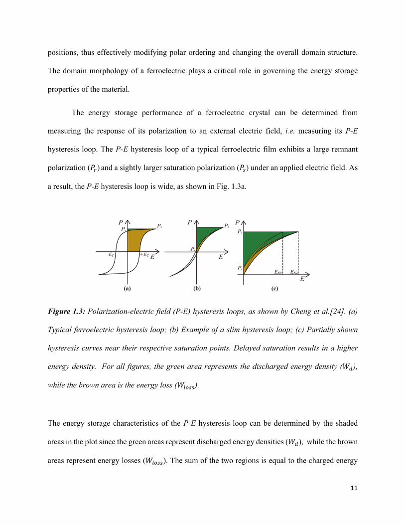
The energy storage performance of a ferroelectric crystal can be determined from
measuring the response of its polarization to an external electric field, i.e. measuring its P-E
hysteresis loop. The P-E hysteresis loop of a typical ferroelectric film exhibits a large remnant
polarization (𝑃D) and a sightly larger saturation polarization (𝑃%) under an applied electric field. As
a result, the P-E hysteresis loop is wide, as shown in Fig. 1.3a.
Figure 1.3: Polarization-electric field (P-E) hysteresis loops, as shown by Cheng et al.[24]. (a)
Typical ferroelectric hysteresis loop; (b) Example of a slim hysteresis loop; (c) Partially shown
hysteresis curves near their respective saturation points. Delayed saturation results in a higher
energy density. For all figures, the green area represents the discharged energy density (𝑊"),
while the brown area is the energy loss (𝑊#$%%).
The energy storage characteristics of the P-E hysteresis loop can be determined by the shaded
areas in the plot since the green areas represent discharged energy densities (𝑊"), while the brown
areas represent energy losses (𝑊#$%%). The sum of the two regions is equal to the charged energy
12
density (𝑊S). It becomes evident that, although a typical ferroelectric has a higher charged energy
density (𝑊S = 𝑊" +𝑊#$%%) compared to a linear dielectric, its energy efficiency (𝜂 = UVUW
) is lower
which results in large energy losses during charge-discharge cycles. In addition, the electrical
breakdown of a ferroelectric is expected to occur shortly after the onset of polarization saturation,
leading to lower applicable electric fields compared to linear dielectrics. To improve the energy
performance of ferroelectric films, a higher energy density and efficiency must be achieved by
decreasing the remnant polarization (𝑃D) and delaying polarization saturation (𝑃%) such that a slim
P-E hysteresis loop can be measured, as shown in Fig. 1.3b. This allows the ferroelectric film to
withstand higher electric fields and store more electrostatic energy with higher efficiencies. There
are several popular approaches used to “slim down” the P-E hysteresis loop of a ferroelectric film
such as using relaxor ferroelectrics [25, 26] or compositions near phase boundaries [27], utilizing
space-charges [28] or interfaces [29], and the inclusion of a dead layer [30].
A promising approach for improving the energy density and efficiency of ferroelectric
films was recently used by Cheng et al.[24]. In their work, a rhombohedral BaZr0.2Ti0.8O3 (BZT)
solid solution and substrate misfit strain are used to create competing polydomain structures in
order to tune the energy performance parameters in ferroelectric films, i.e. “slim down” their P-E
hysteresis loops. A topical review on polydomain structures in ferroelectric and ferroelastic films
has been published by Roytburd et al.[31], overlaying thermodynamic models, phase field
modeling, and experimental studies of such domain structures in epitaxial films. The resulting
ferroelectric BZT thick films were found to exhibit coexisting tetragonal and rhombohedral phases
at room temperature, allowing a delay of polarization saturation as well as lower remnant
polarizations. So far, heterophase polydomain structures have only been observed and reported in
BiFeO3 (BFO)[32-35] and Pb(Zr,Ti)O3 (Zr:PTO)[36] ferroelectrics. These BZT polydomain films
13
demonstrate high energy storage densities and efficiencies compared to single-phase polydomain
ferroelectrics. Furthermore, superior dielectric performances with excellent field and frequency
stabilities are achieved in these films. The key idea behind these favorable properties lies in the
engineering of ultra-adaptive nanoscale domains which can adjust in response to an applied
electrical field. Here, we present the use of optical second harmonic generation polarimetry for
probing these epitaxial ferroelectric BZT thick films in order understand the domain distributions
which govern their high energy performances.
Transmission electron microscopy (TEM) and X-ray diffraction (XRD) measurements on
these BZT thick films verified the presence of mixed rhombohedral and tetragonal phases as elastic
domains. Here, we used polarization-resolved SHG to probe the coexisting tetragonal and
rhombohedral domains within the films. In the reflection geometry, SHG signals were found to
arise predominantly from tetragonal domains growing along the thickness of the films, i.e.
perpendicular to the film-substrate interface. The appearance of rhombohedral signatures in the
reflected SHG intensity profiles with increasing thickness demonstrates symmetry reductions
resulting from strain relaxation as rhombohedral domains become more prevalent. In the
transmission geometry, SHG contributions from the tetragonal domains vanish and signals from
the rhombohedral domains become dominative. Complex transmitted SHG profiles are observed
as a result of elastic rhombohedral polydomains along the thickness of the film. Transmission SHG
measurements provide further evidence of rhombohedral domain growth with increasing film
thickness. We thus provide supporting evidence for the coexistence of mixed tetragonal and
rhombohedral phases as elastic domains in epitaxially strained BZT films at room temperature and
clearly demonstrate an increase in rhombohedral domains with increasing film thickness. These

14
heterophase polydomain nanostructures are directly responsible for the lowered remnant
polarizations and delayed polarization saturations observed in the epitaxial films.
1.3 Scope of Dissertation
Chapter 1 provides a coherent introduction and motivation for our investigation of dc
electric field-induced structural changes at Fe:STO electrode interfaces, structural defect and strain
formation in electrodegraded Fe:STO single crystals, and coexisting tetragonal and rhombohedral
phases in ferroelectric BZT thick films.
Chapter 2 discusses the relevant theoretical foundations and concepts required for
understanding and analyzing the experimental results presented in later chapters. In particular, we
discuss the prevalence of perovskite-type dielectric ceramics, defect chemistry and resistance
degradation of Fe:STO single crystals, strain-field tuning of elastic domains in BZT films, and the
theoretical foundations of optical nonlinearity and SHG.
Chapter 3 provides experimental details on samples, equipment, and optical setups. In
particular, this chapter discusses sample preparation, our femtosecond laser systems and relevant
laser physics principles and parameters, far-field optical SHG polarimetry setups, the confocal
Raman spectroscopy setup, and the photoluminescence spectroscopy setup.
Chapter 4 presents our investigation of local structural changes due to the dc electric field-
induced migration of oxygen vacancies at oxidized and reduced Fe:STO interfaces using optical
SHG in the reflection geometry and photoluminescence spectroscopy. Optical SHG measurements
were used to analyze changes to the second-order susceptibility components while

15
photoluminescence was used to measure fluorescence changes resulting from electronic orbital
transitions.
Chapter 5 presents our study of structural defect and strain formation in electrodegraded
Fe:STO single crystals due to oxygen vacancy migration. Optical SHG in the reflection geometry
was employed to study structural defect accumulation and inhomogeneity across electrodegraded
interfaces. Optical SHG in the transmission geometry and confocal Raman spectroscopy were used
to study structural defect and strain formation across electrocolored bulk regions.
Chapter 6 presents our investigation of coexisting tetragonal and rhombohedral phases in
ferroelectric BZT thick films using optical SHG in the reflection and transmission geometries. In
the reflection geometry, changes to the second-order susceptibility were used to verify an increase
in rhombohedral symmetry signatures with increasing film thickness. In the transmission
geometry, changes in the d-polarized SHG intensities were used to further verify an increase in
rhombohedral symmetry signatures with increasing film thickness.
Chapter 7 summarizes the findings of this dissertation as well as the short-term outlook of
each study.
Any published work or argumentations have been cited accordingly.

16
Chapter 2: Theoretical Background
This chapter goes over relevant theoretical concepts helpful for understanding the
experimental results presented in research chapters 4, 5, and 6. Section 2.1 discusses perovskite-
type dielectrics and how structure plays an important role in determining electrical properties.
Section 2.2 discusses the defect chemistry of Fe:STO while section 2.3 describes the causes and
effects dc voltage-induced resistance degradation in Fe:STO. Section 2.4 provides a brief
discussion of how heterophase polydomain structures in BZT are engineered using epitaxial strain.
Section 2.5 discusses the theoretical concepts behind optical SHG. It should be noted that for
section 2.5, we will only be considering second harmonic radiation from electric dipole sources.
However, quadrupolar and magnetic sources of second harmonic radiation can become significant
in other material systems [37].
2.1 Structure and Dielectric Properties
A dielectric is any insulating material which can be polarized by an imposed electric field.
It is this property which makes dielectric materials ideal for capacitive energy-storage devices. For
a linear, isotropic dielectric the induced polarization across the material can be expressed as:
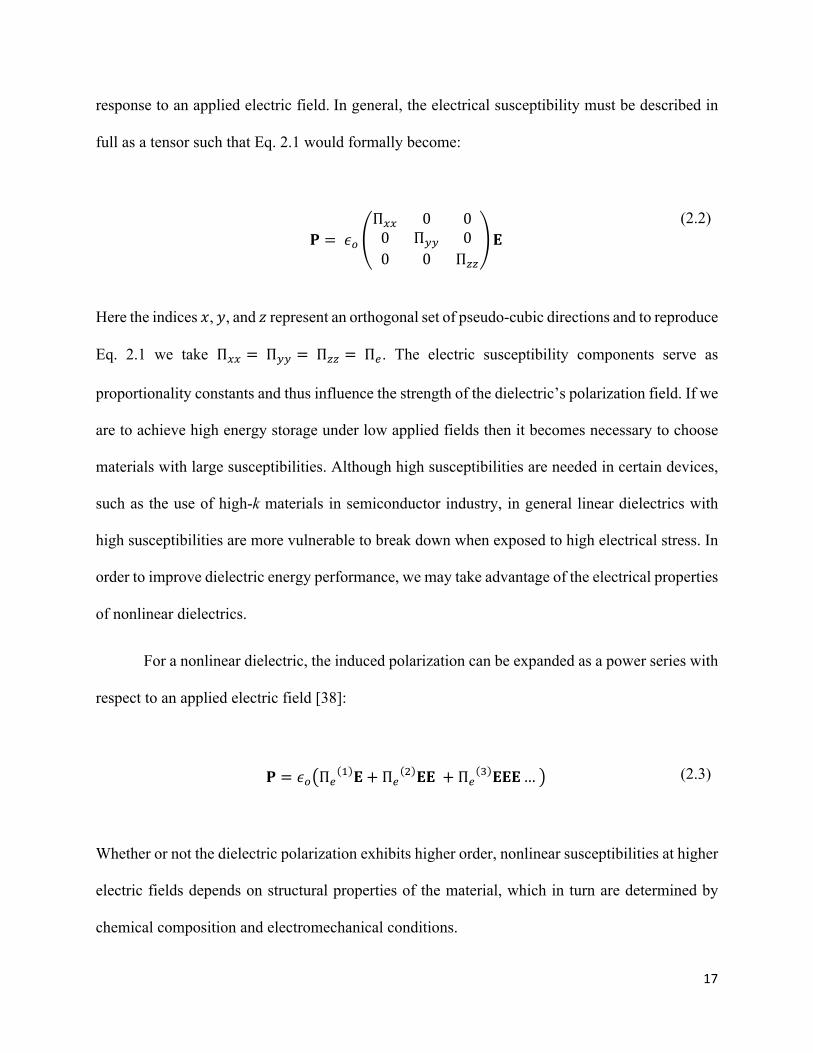
𝐏 = 𝜖$Π[𝐄 (2.1)
Here, 𝜖$ is the permittivity of free space and Π[ is the electrical susceptibility of the dielectric
material. The electrical susceptibility measures how easily the dielectric can be polarized in
17
response to an applied electric field.In general, the electrical susceptibility must be described in
full as a tensor such that Eq. 2.1 would formally become:
𝐏 = 𝜖$
ΠHH 0 00 Π]] 00 0 ΠGG
𝐄 (2.2)
Here the indices 𝑥, 𝑦, and 𝑧 represent an orthogonal set of pseudo-cubic directions and to reproduce
Eq. 2.1 we take ΠHH = Π]] = ΠGG = Π[. The electric susceptibility components serve as
proportionality constants and thus influence the strength of the dielectric’s polarization field. If we
are to achieve high energy storage under low applied fields then it becomes necessary to choose
materials with large susceptibilities. Although high susceptibilities are needed in certain devices,
such as the use of high-k materials in semiconductor industry, in general linear dielectrics with
high susceptibilities are more vulnerable to break down when exposed to high electrical stress. In
order to improve dielectric energy performance, we may take advantage of the electrical properties
of nonlinear dielectrics.
For a nonlinear dielectric, the induced polarization can be expanded as a power series with
respect to an applied electric field [38]:
𝐏 = 𝜖$ Π[ a 𝐄 + Π[ b 𝐄𝐄 + Π[ c 𝐄𝐄𝐄… (2.3)
Whether or not the dielectric polarization exhibits higher order, nonlinear susceptibilities at higher
electric fields depends on structural properties of the material, which in turn are determined by
chemical composition and electromechanical conditions.

18
Ferroelectric ceramics are one the most important groups of nonlinear dielectrics used for
high energy-storage. These insulating materials are composed of polar unit cells which can be
reoriented by an external field, resulting in the polarization switching and reversal effects observed
in P-E hysteresis loops. Over large volumes these dipolar unit cells form regions of uniform,
macroscopic polarization fields known as electric domains. The boundaries between neighboring
electric domains are known as domain walls. Electric domain formation is a consequence of the
lattice seeking to conserve charge neutrality and minimize the total electrostatic energy of the
system. Since each unit cell is polar, local charge carriers reposition themselves to try and oppose
the intrinsic polarity of the material, leading to boundaries between groups of unit cells which
ultimately form domain structures. Electric domains can also be formed as a result of large pinning
polarization fields due to the accumulation of mobile ionic defects, such as oxygen vacancies. This
is known as defect domain stabilization and can lead to breakdown mechanisms such as aging. In
section 2.4, we will discuss how strain effects may lead to the formation of additional domains,
known as elastic domains.
Ferroelectricity in ceramic materials is inseparable from structural symmetry since it is
only allowed in non-centrosymmetric crystal point groups. The 21, non-centrosymmetric point
groups are well-documented: 1, 2, 𝑚, 222, 𝑚𝑚2, 4, 4, 422, 4𝑚𝑚, 42𝑚, 3, 32, 3𝑚, 6, 6, 622,
6𝑚𝑚, 62𝑚, 23, 432, and 43𝑚 [39, 40]. The possible polar domain variants, or domain
polarization directions, accessible within a ferroelectric can be determined from its crystal point
group symmetry. As an example, Fig. 2.1 shows cubic (Pm3m), tetragonal (4mm), and
rhombohedral (3m) unit cells with their possible polar axes shown as red arrows [41]. Due to
centrosymmetry, the cubic cell is non-polar and does not exhibit an electric dipole moment. For
tetragonal symmetry, the polarization can point towards any of the 6 pseudo-cubic faces of the unit

19
cell depending on the position of the tetragonal c-axis. For rhombohedral symmetry, the
polarization can point towards any of the 8 pseudo-cubic corners of the unit cell depending on the
tilt directions. In general, the lower degree of symmetry, the more possible polarization directions
there are. These symmetries also determine domain wall formation, since these boundaries form
between neighboring electric domains. Materials exhibiting tetragonal symmetry can only form
90o and 180o electric domain walls, while materials exhibiting rhombohedral symmetry, a trigonal
structure, will typically form 180o electric domain walls.
Figure 2.1: Examples of polar domain variants in ferroelectric materials exhibiting tetragonal
(4mm) and rhombohedral (3m) symmetry. On the left a centrosymmetric cubic unit cell is shown
for reference. In the middle, a non-centrosymmetric tetragonal unit cell is shown where the solid
arrow points in the direction of the 100 polarization and dashed arrows point in other 5 possible
directions. On the right, a non-centrosymmetric rhombohedral unit cell is shown where the solid
arrow points in the direction of the 111 polarization and dashed arrows point in the other 7
possible directions.
20
2.1.1 Perovskite-type Ceramics
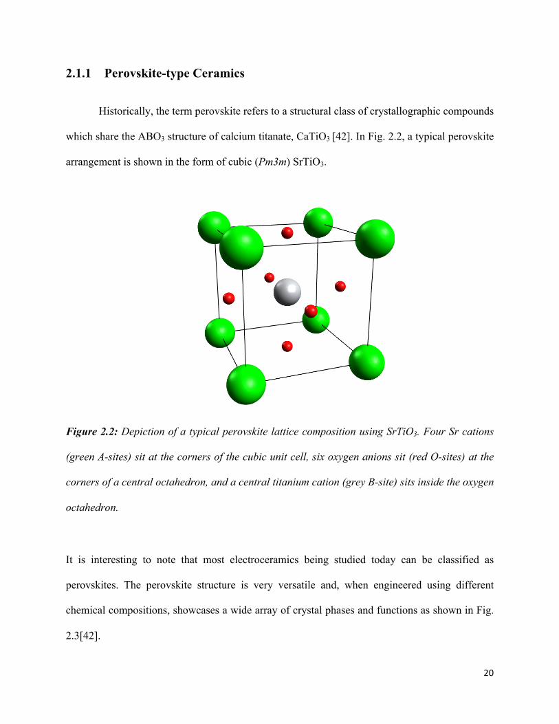
Historically, the term perovskite refers to a structural class of crystallographic compounds
which share the ABO3 structure of calcium titanate, CaTiO3 [42]. In Fig. 2.2, a typical perovskite
arrangement is shown in the form of cubic (Pm3m) SrTiO3.
Figure 2.2: Depiction of a typical perovskite lattice composition using SrTiO3. Four Sr cations
(green A-sites) sit at the corners of the cubic unit cell, six oxygen anions sit (red O-sites) at the
corners of a central octahedron, and a central titanium cation (grey B-site) sits inside the oxygen
octahedron.
It is interesting to note that most electroceramics being studied today can be classified as
perovskites. The perovskite structure is very versatile and, when engineered using different
chemical compositions, showcases a wide array of crystal phases and functions as shown in Fig.
2.3[42].
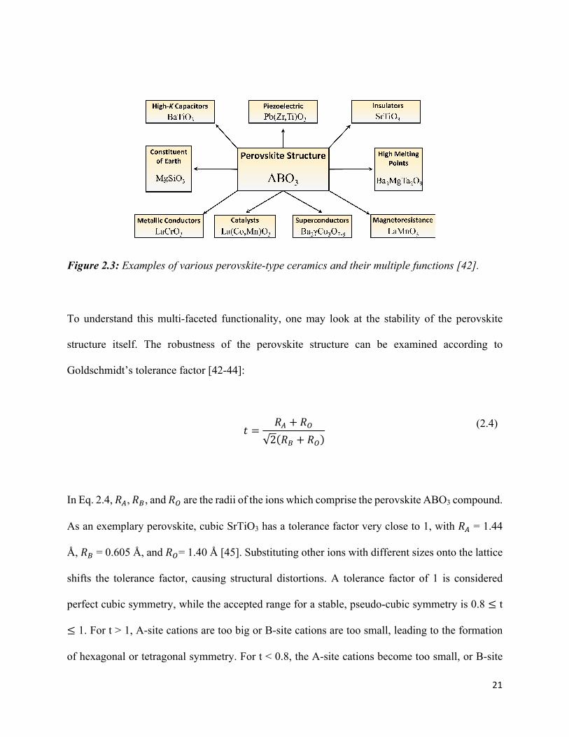
21
Figure 2.3: Examples of various perovskite-type ceramics and their multiple functions [42].
To understand this multi-faceted functionality, one may look at the stability of the perovskite
structure itself. The robustness of the perovskite structure can be examined according to
Goldschmidt’s tolerance factor [42-44]:
𝑡 =𝑅j + 𝑅k2 𝑅A + 𝑅k
(2.4)
In Eq. 2.4, 𝑅j, 𝑅A, and 𝑅k are the radii of the ions which comprise the perovskite ABO3 compound.
As an exemplary perovskite, cubic SrTiO3 has a tolerance factor very close to 1, with 𝑅j = 1.44
Å, 𝑅A = 0.605 Å, and 𝑅k= 1.40 Å [45]. Substituting other ions with different sizes onto the lattice
shifts the tolerance factor, causing structural distortions. A tolerance factor of 1 is considered
perfect cubic symmetry, while the accepted range for a stable, pseudo-cubic symmetry is 0.8 ≤ t
≤ 1. For t > 1, A-site cations are too big or B-site cations are too small, leading to the formation
of hexagonal or tetragonal symmetry. For t < 0.8, the A-site cations become too small, or B-site

22
cations become too large, leading to the formation of orthorhombic and rhombohedral symmetries.
alternative structures. For t < 0.7, A-site and B-site ions have similar radii and result in various
trigonal symmetries [46]. Thus, the tolerance factor can be used to predict the symmetry and
stability of perovskite-type ceramics [47]. In other words, the perovskite structure acts as a stable
framework in which different ions can be fitted. The chemical composition and structural phase of
the resulting perovskite determine its functionality.
2.2 Defect Chemistry in Fe:STO
Mobile charge defects such as oxygen vacancies, holes, and electrons contribute to the
conductivity and polarization of acceptor-doped SrTiO3 crystals. For Fe-doped SrTiO3 (Fe:STO)
in the dilute doping regime, where [Ti] >> [Fe], Ti sites are partially filled by Fe atoms exhibiting
mixed Fe3+ and Fe4+ valence states such that one can take the following mass conservation
condition[4, 48]:
[𝐹𝑒]E$E;# = [𝐹𝑒co] + [𝐹𝑒po] (2.5)
In Eq. 2.5, [Fe3+] and [Fe4+] represent the concentrations (number density) of Fe3+ and Fe4+ ions in
the crystal, respectively. Due to the mixed valence states of the acceptor-dopant Fe, charge
neutrality of the unit cell is not always conserved. For example, consider both tetravalent and
trivalent Fe-doped SrTiO3 unit cells. We have the following two charge conservation equations:
4𝑆𝑟bo +𝐹𝑒po + 6𝑂bt → 0 (2.6a)

23
4𝑆𝑟bo +𝐹𝑒co + 6𝑂bt → −1 (2.6b)
In order to maintain charge neutrality with respect to the crystal lattice, oxygen vacancies form in
the first coordination shell of Fe3+ defect centers, and we obtain the following charge equation:
4𝑆𝑟bo +𝐹𝑒co + 5𝑂bt → +1 (2.6c)
Due to this net positive charge, excess electrons in the crystal will tend to crowd oxygen vacancy
defects to compensate. Thus, the following conservation condition appears for the crystal:
2 𝑉k∙∙ + ℎ = [𝐹𝑒co] + [𝑒] (2.7)
In Eq. 2.7, [𝑉k∙∙], ℎ , and [𝑒] are the concentrations of oxygen vacancies, holes, and free electrons
in the crystal. The symbol for the doubly ionized oxygen vacancy, 𝑉k∙∙, comes from Kröger-Vink
notation where the V stands for vacancy, the O stands for the oxygen site, and the two dots
represent that the point defect has an effective charge of +2 with respect to the lattice. Singly
ionized oxygen vacancies, 𝑉k∙ , with an effective charge of +1 can also form by accepting free
electrons when free electron concentrations are high. In common cases where free electronic
carrier concentrations are very low, Eq. 2.7 can be simplified [4, 48]:
2 𝑉k∙∙ ≈ [𝐹𝑒co] (2.8)
As a result, the oxygen vacancy concentration within the crystal at low temperatures (T ≲ 400oC)
can be estimated based on the Fe-doping concentration [7, 49, 50].
24
Fe:STO is a mixed ionic and electronic conductor and its total conductivity can be
expressed as follows:
𝜎E$E;# = 𝜎{| + 𝜎[ + 𝜎} (2.9)
In Eq. 2.9, 𝜎{|, 𝜎[, and 𝜎} represent the oxygen vacancy, electron, and hole conductivities,
respectively. These conductivities have been shown to exhibit a strong dependence on annealing
oxygen partial pressure and temperature[15, 16]. The defect chemistry of an Fe:STO single crystal
can thus be tuned according to both of these annealing parameters for electrochemical reduction
and oxidation treatments. Fe:STO contains much higher oxygen vacancy concentrations compared
to electronic carriers at nearly all temperatures, resulting in oxygen vacancies playing an unrivaled
role during dc electric field-induced degradation compared to other mobile point defects[10, 15,
16, 51].
The concentration of oxygen vacancy defects as a function of temperature in the crystal
can be approximated by considering the Gibbs free energy of the system [44, 52]:
𝐺 = 𝐻 − 𝑇𝑆 (2.10)
In Eq. 2.10, 𝐺 is the Gibbs free energy, 𝐻 is the total enthalpy of the crystal, T is the temperature,
and 𝑆 is the entropy of the crystalline system. The entropy consists of a vibrational (phonon
entropy) and configurational (configurational entropy) term such that:
𝑆 = 𝑆�6� + 𝑆S$�) (2.11)
25
Here, the enthalpy and vibrational entropy can be taken to be proportional to the number of
vacancies, and the configurational entropy is a function of the number of vacancies[52] such that
we can transform Eq. 2.10 as follows:
∆𝐺 = 𝑁{ ∆𝐻 − 𝑇∆𝑆�6� − 𝑇∆𝑆S$�)(𝑁{) (2.12)
Here, 𝑁{ represents the number of vacancies in the crystal lattice. The configurational entropy can
be expressed by considering the total number of arrangements between vacancies and oxygen sites
in the crystal, 𝑊 = 𝑁𝑁{
= �!�t�� !��!
. Thus, the configurational entropy can be expressed as:
𝑆S$�)(𝑁{) = 𝑘�ln𝑁!
𝑁 − 𝑁{ !𝑁{! (2.13)
Here, 𝑘� represents Boltzmann’s constant and N is the total number of vacancies and oxygen sites
in the crystal. In the thermodynamic limit (N >> 1), 𝑆S$�)(𝑁{) can be simplified using Stirling’s
approximation, 𝑙𝑛 𝑁! ≈ 𝑁𝑙𝑛 𝑁 − 𝑁. Eq. 2.13 becomes:
𝑆S$�) = 𝑁𝑘�ln𝑁
𝑁 − 𝑁{− 𝑁{𝑘�ln
𝑁{𝑁 − 𝑁{
(2.14)
Now, in order to find the equilibrium condition for the number of vacancies, we must solve for the
Gibbs free energy minimum by differentiating and setting the expression to zero:
𝑑∆𝐺𝑑𝑁{
= ∆𝐻 − 𝑇∆𝑆�6� − 𝑇𝑑𝑆S$�)𝑑𝑁{
= 0 (2.15)

26
With care, the derivative of the configurational entropy with respect to the vacancy number
becomes:
𝑑𝑆S$�)𝑑𝑁{
=𝑑𝑑𝑁{
𝑁𝑘�ln𝑁
𝑁 − 𝑁{− 𝑁{𝑘�ln
𝑁{𝑁 − 𝑁{
= −𝑘�𝑙𝑛𝑁{
𝑁 − 𝑁{
(2.16)
And Eq. 2.15 can be written as:
𝑁{𝑁 − 𝑁{
= 𝑒������ 𝑒
t∆���� (2.17)
Since the number of vacancies is typically much less than the total number of lattice sites in a
crystal, ���t��
can approach the concentration of oxygen vacancies, ���t��
≈ ���≈ [𝑁{]. If the
vibrational entropy and enthalpy of the system are known, then the equilibrium concentration of
oxygen vacancies at a specified temperature can be estimated. The two significant enthalpies for
oxygen vacancies are the so-called generation and migration enthalpies [53, 54]. The generation
enthalpy corresponds to the potential energy required for the formation of an oxygen vacancy
while the migration enthalpy corresponds to the potential energy required for a vacancy to hop
from one site to another, which is how diffusion occurs within the lattice. At higher temperatures,
additional thermal energy facilitates site hopping for oxygen vacancies in the system, thus
increasing their mobility. Measured ∆𝐻�6B values typically range between ~0.6–0.7 eV in
STO[55] and dilutely-doped STO[15, 16] single crystals.
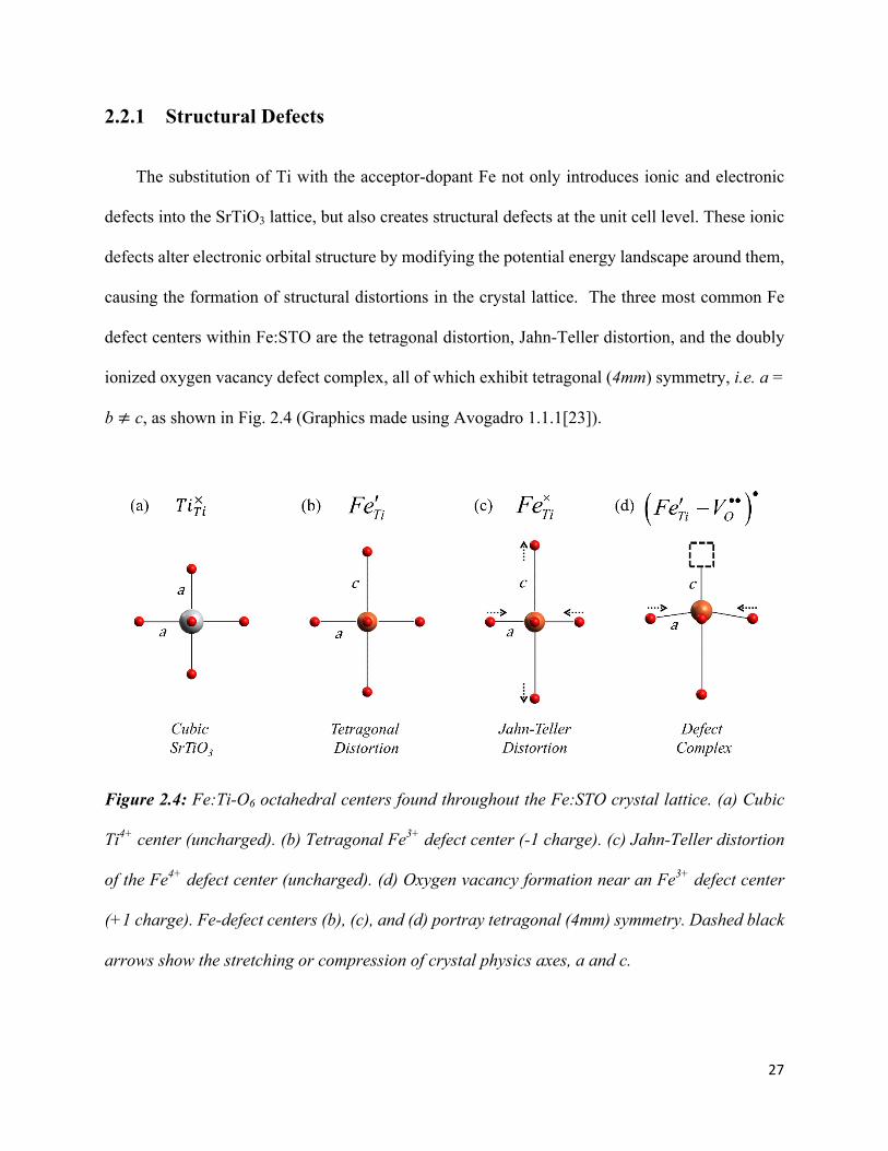
27
2.2.1 Structural Defects
The substitution of Ti with the acceptor-dopant Fe not only introduces ionic and electronic
defects into the SrTiO3 lattice, but also creates structural defects at the unit cell level. These ionic
defects alter electronic orbital structure by modifying the potential energy landscape around them,
causing the formation of structural distortions in the crystal lattice. The three most common Fe
defect centers within Fe:STO are the tetragonal distortion, Jahn-Teller distortion, and the doubly
ionized oxygen vacancy defect complex, all of which exhibit tetragonal (4mm) symmetry, i.e. a =
b ≠ c, as shown in Fig. 2.4 (Graphics made using Avogadro 1.1.1[23]).
Figure 2.4: Fe:Ti-O6 octahedral centers found throughout the Fe:STO crystal lattice. (a) Cubic
Ti4+ center (uncharged). (b) Tetragonal Fe3+ defect center (-1 charge). (c) Jahn-Teller distortion
of the Fe4+ defect center (uncharged). (d) Oxygen vacancy formation near an Fe3+ defect center
(+1 charge). Fe-defect centers (b), (c), and (d) portray tetragonal (4mm) symmetry. Dashed black
arrows show the stretching or compression of crystal physics axes, a and c.
28
It is important to note that for both undegraded STO and Fe:STO, unit cells transition from
cubic (Pm3m) symmetry to tetragonal (4mm) symmetry near surfaces due to atomic displacements
along the normal axis[56, 57]. Fe:Ti valence state changes and local oxygen ion migrations govern
the formation of structural defects in Fe:STO during oxygen vacancy migration. In the tetragonal
distortion, shown in Fig. 2.4b an Fe3+ cation occupies a Ti4+ site and fully coordinates itself to six
nearest oxygen neighbors in the octahedron. This defect is negatively charged with respect to the
crystal lattice. In the Jahn-Teller distortion, an Fe4+ cation occupies a Ti4+ site and fully coordinates
itself to six nearest oxygen neighbors in the octahedron. In order to avoid electronic d-orbital
degeneracies around the Fe4+ cation, the octahedron undergoes a geometric deformation which
results in oxygen bond expansion and contraction along the c- and a-axis, respectively, as shown
in Fig. 2.4c[58, 59]. This defect has a neutral charge with respect to the surrounding crystal lattice.
We note that Fe4+ cations may also occupy Ti4+ sites without introducing a Jahn-Teller distortion.
For the oxygen vacancy defect complex, as shown in Fig. 2.4d, an Fe3+ cation occupies a Ti4+ site
and coordinates itself with five nearest oxygen neighbors and one vacancy. The vacancy results in
a displacement of the central Fe3+ cation and bending of the a-axis oxygen bonds. This defect is
positively charged with respect to the crystal lattice [4, 60-62]. As a result of oxygen vacancy
demixing in Fe:STO, local Fe4+ valence states reduce to Fe3+ valence states in the cathode region.
Meanwhile, oxygen ions and holes pile up near the anode and lead to the local oxidation of Fe3+
valence states to Fe4+ valence states. Thus, Fe4+ structural defects, such as tetragonal and Jahn-
Teller distortions, form in the anode region while oxygen vacancy defect complexes form in the
cathode region.

29
2.3 Resistance Degradation in Fe:STO
2.3.1 Reduction Model
In the reduction model, the high mobility and concentration of oxygen vacancies are
described as the dominating contributors to voltage-induced resistance degradation in Fe:STO[7,
10, 17, 63]. Under the influence of a dc electrical field, positively charged oxygen vacancies
migrate towards the cathode while oxygen ions migrate towards the anode. Due to the electrodes
blocking effect on ionic currents at low temperatures (T ≲ 400oC), oxygen vacancies pile up.
Consequently, an electrochemical p-n junction is formed, where the anodic region becomes p-type
conducting and the cathodic region becomes n-type conducting, as a result of local electrons
compensating the accumulation of vacancies at the cathode in an attempt to conserve charge
neutrality [5-7]. The rise in electronic conductivity at the electrochemically reduced cathode leads
to a decrease in insulation-resistance. An increase in leakage current across the dielectric ceramic
by two orders of magnitude occurs, diminishing the materials capacitive ability.
2.3.2 Electrocoloration
A process known as electrocoloration also occurs in Fe:STO as a result oxidation state
changes to the transition metal, Fe, in the anodic region. As the external electric field drives oxygen
vacancies away from the anode, the Fe4+ concentration increases significantly due to a loss of local
electronic carriers. The increased concentration of Fe4+ in the anode leads to a visible darkening
of the anodic region due to local increases in optical absorption[64]. This process has been shown
experimentally to be reversible by reversing the electrical field for STO with various transition

30
metal dopants such as Ni, Mo, and Al [65]. It has also been shown that the ambient oxygen pressure
has no effect on the electrocoloration process [20].
2.3.3 Electrostriction
In addition to driving oxygen vacancy migration, dc electrical stress also induces forces on
the crystal lattice which cause a structural deformation known as electrostriction[66].
Electrostriction is an electromechanical effect which results from the coupling between strain and
an electrical field[38, 67-69]. When electrostrictive strain occurs in a dielectric ceramic, the
material typically undergoes a lattice expansion along the applied electric field axis as a result of
field-induced ionic displacements. The elastic properties of the ceramic can also lead to
constrictive deformations perpendicular to the applied field axis[67]. The combined effects of
defect accumulations at the anode and cathode and electrostrictive distortions in the material lead
to a redistribution of structural strain, especially over electrocoloration boundaries which separate
electrochemically reduced and oxidized bulk regions. Computational studies have provided strong
evidence for increased oxygen vacancy mobility due to structural symmetry breaking and strain.
Density Functional Theory (DFT) calculations have shown that strain compromises oxygen bond
strengths and can lead to decreases in both oxygen vacancy defect formation energies and
migration energy barriers [70, 71]. To this point, structural defect and strain formation in Fe:STO
are predicted to increase vacancy mobility, ultimately contributing to the resistance degradation
process.
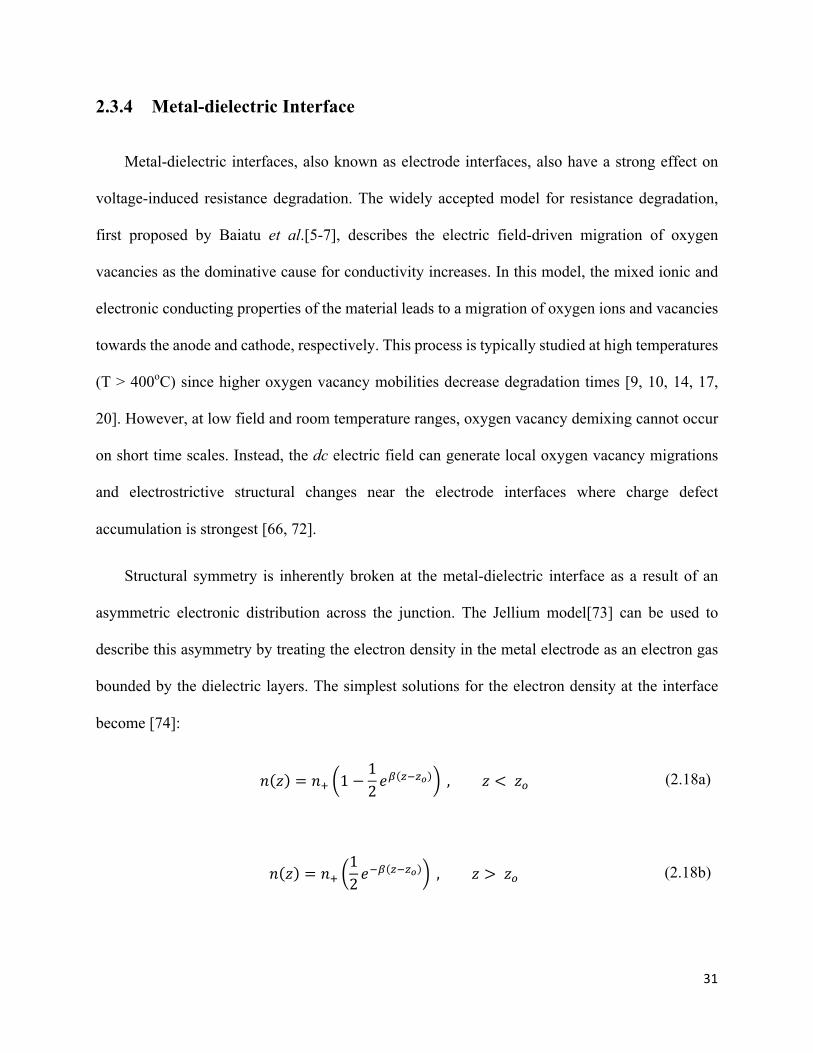
31
2.3.4 Metal-dielectric Interface
Metal-dielectric interfaces, also known as electrode interfaces, also have a strong effect on
voltage-induced resistance degradation. The widely accepted model for resistance degradation,
first proposed by Baiatu et al.[5-7], describes the electric field-driven migration of oxygen
vacancies as the dominative cause for conductivity increases. In this model, the mixed ionic and
electronic conducting properties of the material leads to a migration of oxygen ions and vacancies
towards the anode and cathode, respectively. This process is typically studied at high temperatures
(T > 400oC) since higher oxygen vacancy mobilities decrease degradation times [9, 10, 14, 17,
20]. However, at low field and room temperature ranges, oxygen vacancy demixing cannot occur
on short time scales. Instead, the dc electric field can generate local oxygen vacancy migrations
and electrostrictive structural changes near the electrode interfaces where charge defect
accumulation is strongest [66, 72].
Structural symmetry is inherently broken at the metal-dielectric interface as a result of an
asymmetric electronic distribution across the junction. The Jellium model[73] can be used to
describe this asymmetry by treating the electron density in the metal electrode as an electron gas
bounded by the dielectric layers. The simplest solutions for the electron density at the interface
become [74]:
𝑛 𝑧 = 𝑛o 1 −12 𝑒
� GtG| , 𝑧 < 𝑧$ (2.18a)
𝑛 𝑧 = 𝑛o12 𝑒
t� GtG| , 𝑧 > 𝑧$ (2.18b)

32
In Eq. 2.18, 𝛽 is a scaling parameter to be determined, 𝑧$ is the position where the electronic
density is half of its bulk value, and 𝑛o is the ionic density in the bulk of the metal electrode. The
electron density inside the metal tends to the ionic density in order to conserve charge neutrality
within the bulk of the metal, although this is not true at the surface of the metal. Fig. 2.5 shows the
electron distribution between the metal electrode and dielectric layers which results in symmetry
breaking along the z-axis.
Figure 2.5: Electronic distribution at a metal-dielectric interface, approximated using Eq. 2.18.
The light grey shaded region represents the metal electrode, while the white region represents the
dielectric. The red solid curve signifies the electronic density across the junction.
The electronic distribution and electrical response of the metal-dielectric interface are further
complicated according to what kind of conducting contact is formed. For example, if the metal is
platinum (Pt) and the dielectric is Fe-doped or undoped SrTiO3 then, due to work function
differences existing between the electrode and dielectric layers, the formation of a Schottky
junction will take place [75]. An energy barrier, known as the Schottky Barrier, forms between the

33
metal and dielectric which leads to a rectifying behavior [76]. In addition, the Schottky Barrier
also leads to the formation of an interfacial depletion region. The depletion region is a thin
insulating region which becomes depleted of electronic carriers, leaving behind only ionic defects.
Intrinsic electric fields can form across this region as a result of electronic carrier build up on
opposite ends of the region. Under the influence of an external electric field, the depletion region
can break down, quenching the intrinsic electric field at the interface.
2.4 Domain Structures in BZT Films
At room temperature, barium titanate (BaTiO3, BTO) films exhibit tetragonal (4mm)
symmetry, with in-plane and out-of-plane lattice parameters of a = 3.992 Å and c = 4.036 Å,
respectively. Within the BTO unit cell, the central Ti4+ cation is displaced with respect to the
surrounding oxygen octahedron, resulting in the formation of an electric dipole moment, as
previously shown in Fig. 1.2. Thus, BTO is a ferroelectric ceramic with tetragonal (4mm)
symmetry at room temperature. Through the use of zirconium (Zr4+) as a B-site dopant, the
equilibrium phase of BZT can be transitioned to rhombohedral (3m) symmetry. The BZT
equilibrium phase as a function of Zr-doping amount is shown in Fig. 2.6, according to the solid
lines.
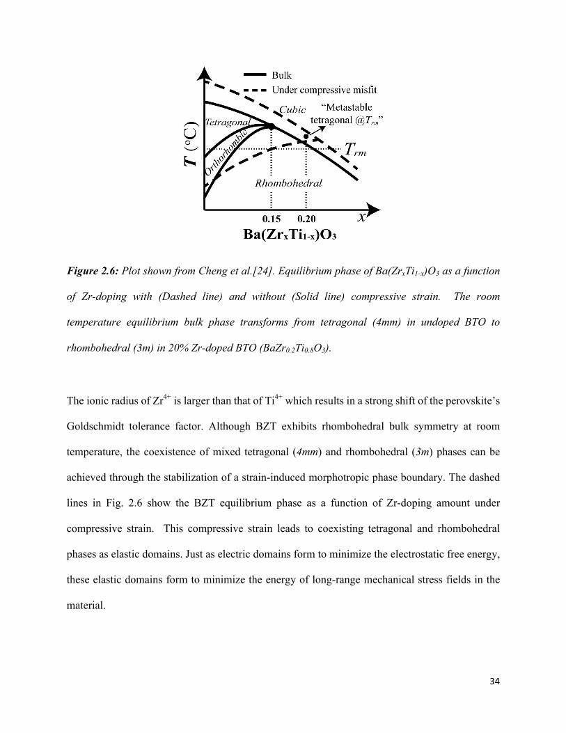
34
Figure 2.6: Plot shown from Cheng et al.[24]. Equilibrium phase of Ba(ZrxTi1-x)O3 as a function
of Zr-doping with (Dashed line) and without (Solid line) compressive strain. The room
temperature equilibrium bulk phase transforms from tetragonal (4mm) in undoped BTO to
rhombohedral (3m) in 20% Zr-doped BTO (BaZr0.2Ti0.8O3).
The ionic radius of Zr4+ is larger than that of Ti4+ which results in a strong shift of the perovskite’s
Goldschmidt tolerance factor. Although BZT exhibits rhombohedral bulk symmetry at room
temperature, the coexistence of mixed tetragonal (4mm) and rhombohedral (3m) phases can be
achieved through the stabilization of a strain-induced morphotropic phase boundary. The dashed
lines in Fig. 2.6 show the BZT equilibrium phase as a function of Zr-doping amount under
compressive strain. This compressive strain leads to coexisting tetragonal and rhombohedral
phases as elastic domains. Just as electric domains form to minimize the electrostatic free energy,
these elastic domains form to minimize the energy of long-range mechanical stress fields in the
material.

35
2.4.1 Heterophase Polydomain Structures
Phase refers to the structural symmetry of the crystalline unit cell while domain refers to
the orientation of the electrical polarization. Thus, ferroelectric films exhibiting heterophase
polydomain structures consist of multiple polar domain variants of more than one crystalline
phase. The ferroelectric BZT thick films discussed in this dissertation exhibit heterophase
polydomain structures due to their coexisting rhombohedral (3m) and tetragonal (4mm) crystal
phases. Rhombohedral phases have 8 pseudo-cubic 111 polar domain orientations while
tetragonal phases have 6 pseudo-cubic 001 polar domain orientations, as shown previously in
Fig. 2.1. Evidently, heterophase polydomain structures have valuable energy storage properties as
a result of how they respond to external dc electrical stress. During field application, heterophase
polydomain structures can absorb additional electrical energy by transitioning into single phase
structures, thus delaying the saturation of their polarization. This delay leads to larger applicable
electric fields and, consequently, higher breakdown field strengths. As a result, energy densities in
films exhibiting heterophase polydomain structures are expected to surpass the energy densities of
single phase films. The energy storage properties of ferroelectric films exhibiting heterophase
polydomain structures can be tuned even further by taking advantage of mechanical stresses. Since
these domain structures are elastic in nature, i.e. stabilized as a result of the minimization of elastic
energy, mechanical constraints such as film thickness and substrate species have a strong effect on
the equilibrium bulk structures formed during epitaxial growth[32, 33, 77]. Consequently, tuning
the domain architecture results in a tuning of the remnant and saturation polarization and, by
extension, the energy storage properties of the film.
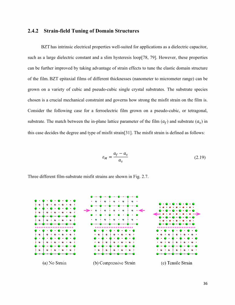
36
2.4.2 Strain-field Tuning of Domain Structures
BZT has intrinsic electrical properties well-suited for applications as a dielectric capacitor,
such as a large dielectric constant and a slim hysteresis loop[78, 79]. However, these properties
can be further improved by taking advantage of strain effects to tune the elastic domain structure
of the film. BZT epitaxial films of different thicknesses (nanometer to micrometer range) can be
grown on a variety of cubic and pseudo-cubic single crystal substrates. The substrate species
chosen is a crucial mechanical constraint and governs how strong the misfit strain on the film is.
Consider the following case for a ferroelectric film grown on a pseudo-cubic, or tetragonal,
substrate. The match between the in-plane lattice parameter of the film (𝑎)) and substrate (𝑎%) in
this case decides the degree and type of misfit strain[31]. The misfit strain is defined as follows:
𝜀� =𝑎) − 𝑎%𝑎%
(2.19)
Three different film-substrate misfit strains are shown in Fig. 2.7.
37
Figure 2.7: Shows different misfit strains which can form between the epitaxial ferroelectric film
and the tetragonal substrate. (a) The case where 𝑎) = 𝑎% doesn’t result in a misfit strain; (b) The
case where 𝑎) > 𝑎% leads to a compressive strain on the film; (c) The case where 𝑎) < 𝑎% leads
to an expansive tensile strain on the film. Short-dashed lines mark the interface sites for clarity.
Fig. 2.7a shows the homoepitaxial growth scenario, when 𝑎) = 𝑎% and the misfit strain is zero.
The lack of a misfit strain has no effect on the structure of the film. Fig. 2.7b and Fig. 2.7c show
the two heteroepitaxial growth scenarios where 𝑎) ≠ 𝑎% and the misfit strain can result in a
compressive or tensile strain on the film lattice. Under compressive strain, the film lattice squeezes
along the in-plane direction to minimize mechanical stresses from the substrate. In contrast, under
a tensile, or expansive, strain the film lattice elongates along the in-plane direction to minimize
such stresses. Due to the tensor nature of mechanical stresses, compressive straining of the film
lattice leads to expansion along the film’s thickness while tensile straining of the film leads to a
compression along the film’s thickness. In this work, compressive misfit strains were utilized since
the in-plane lattice parameter of BZT is approximately a = 4.12 Å, while the lattice parameters of
the SrTiO3 (STO), LaAlO3 (LAO), and (La,Sr)(Al,Ta)O3 (LSAT) substrates are 3.905 Å, 3.79 Å,
and 3.87 Å, respectively[34]. The compressive misfit strain brings BZT’s tetragonal and
rhombohedral equilibrium phases closer together at room temperatures, thus satisfying the
requirement for the formation of mixed tetragonal and rhombohedral domains, i.e. heterophase
polydomain structure.
Thickness of the film also plays a significant role in influencing the elastic domain
architecture. 20% Zr-doped BTO exhibits rhombohedral bulk symmetry at room temperature,
however, the film is compressively strained near the tetragonal substrate. This results in the BZT

38
lattice favoring tetragonal domain formation near the interface. The strain-fields generated by
inter-locking, tetragonal domains formed at the substrate interface propagate along the films
thickness, dominating in thin films. In thicker films (350 nm or more), strain-field relaxation takes
place away from the substrate and results in a lowering of crystalline symmetry so that tetragonal
phases can transition into rhombohedral ones. The mixture of rhombohedral and tetragonal
domains in a mechanically constrained ferroelectric film can thus be modulated using thickness
and substrate strain effects. Superior dielectric properties are accomplished through the formation
of such heterophase polydomain structures[80]. These complex elastic domain structures are able
to undergo versatile structural evolutions under the influence of an external electric field, thus
leading to favorable results such as lower remnant polarization and delayed saturation. This
ultimately helps lower energy density loss during charge-discharge cycles and increase storable
energy densities.
2.5 Optical Second Harmonic Generation
When light strikes a material, the electric field of the optical wave drives charge oscillations
along chemical bonds. Within the dipole approximation, these charge oscillations lead to an
oscillating electric polarization which then re-radiates its own electric field as governed by
Maxwell’s wave equation:
−∇× ∇×𝑬 +
𝑛b
𝑐b𝜕b𝑬𝜕𝑡b = 𝜇$
𝜕b𝑷𝜕𝑡b
(2.20)
In Eq. 2.20, 𝑛 is the refractive index of the material, c is the speed of light in free space, 𝜇$ is the
permeability of free space, and the optically induced polarization field, 𝑷(𝒓, 𝑡), acts as a source of

39
new radiation (𝑬(𝒓, 𝑡)). In general, this optically induced polarization must be expanded as a power
series with respect to the electric field of the incident light to account for nonlinear sources of
radiation.
𝑃 𝑡 = 𝜖$ 𝜒 a 𝐸 𝑡 + 𝜒 b 𝐸 𝑡 b + 𝜒 c 𝐸 𝑡 c + ⋯+𝜒 � 𝐸 𝑡 � (2.21)
Higher power terms (n > 1) give rise to nonlinear optical effects, however, the second-order
polarization is the most important term to consider since this term gives rise to the optical process
known as second harmonic generation (SHG).
In the nonlinear optical process of SHG, two photons of frequency 𝜔 are absorbed and a
photon of frequency 2𝜔 is emitted, as shown in Fig. 2.8.
Figure 2.8: Energy diagram for optical second harmonic generation. Two photons of energy E =
ℏ𝜔 are absorbed, exciting the system to a virtual state. Then, one photon of energy E = 2ℏ𝜔 is
emitted as the system returns to its ground state.
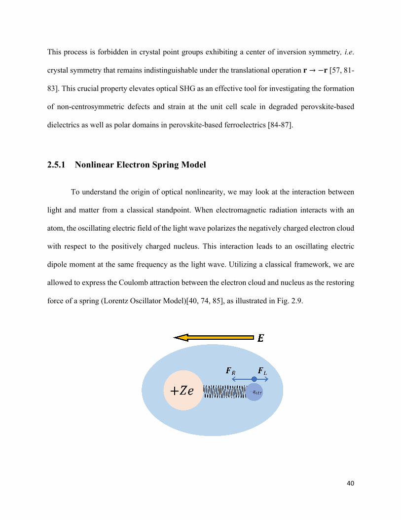
40
This process is forbidden in crystal point groups exhibiting a center of inversion symmetry, i.e.
crystal symmetry that remains indistinguishable under the translational operation 𝐫 → −𝐫 [57, 81-
83]. This crucial property elevates optical SHG as an effective tool for investigating the formation
of non-centrosymmetric defects and strain at the unit cell scale in degraded perovskite-based
dielectrics as well as polar domains in perovskite-based ferroelectrics [84-87].
2.5.1 Nonlinear Electron Spring Model
To understand the origin of optical nonlinearity, we may look at the interaction between
light and matter from a classical standpoint. When electromagnetic radiation interacts with an
atom, the oscillating electric field of the light wave polarizes the negatively charged electron cloud
with respect to the positively charged nucleus. This interaction leads to an oscillating electric
dipole moment at the same frequency as the light wave. Utilizing a classical framework, we are
allowed to express the Coulomb attraction between the electron cloud and nucleus as the restoring
force of a spring (Lorentz Oscillator Model)[40, 74, 85], as illustrated in Fig. 2.9.
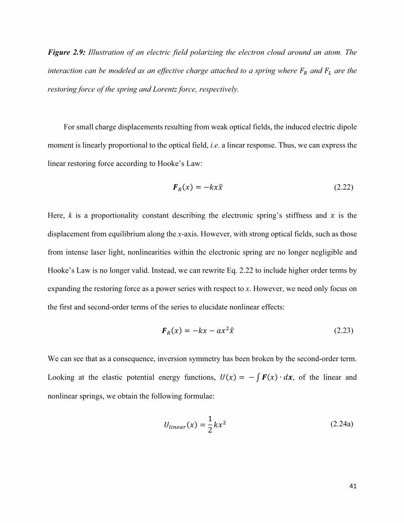
41
Figure 2.9: Illustration of an electric field polarizing the electron cloud around an atom. The
interaction can be modeled as an effective charge attached to a spring where 𝐹0 and 𝐹1 are the
restoring force of the spring and Lorentz force, respectively.
For small charge displacements resulting from weak optical fields, the induced electric dipole
moment is linearly proportional to the optical field, i.e. a linear response. Thus, we can express the
linear restoring force according to Hooke’s Law:
𝑭0 𝑥 = −𝑘𝑥𝑥 (2.22)
Here, k is a proportionality constant describing the electronic spring’s stiffness and 𝑥 is the
displacement from equilibrium along the x-axis. However, with strong optical fields, such as those
from intense laser light, nonlinearities within the electronic spring are no longer negligible and
Hooke’s Law is no longer valid. Instead, we can rewrite Eq. 2.22 to include higher order terms by
expanding the restoring force as a power series with respect to x. However, we need only focus on
the first and second-order terms of the series to elucidate nonlinear effects:
𝑭0 𝑥 = −𝑘𝑥 − 𝑎𝑥b𝑥 (2.23)
We can see that as a consequence, inversion symmetry has been broken by the second-order term.
Looking at the elastic potential energy functions, 𝑈 𝑥 = − 𝑭 𝑥 ∙ 𝑑𝒙, of the linear and
nonlinear springs, we obtain the following formulae:
𝑈#6�[;D 𝑥 =12𝑘𝑥
b (2.24a)
42
𝑈�$�#6�[;D 𝑥 =12𝑘𝑥
b +13𝑎𝑥
c (2.24b)
It can easily be verified that 𝑈#6�[;D −𝑥 = 𝑈#6�[;D 𝑥 from Eq. 2.24a, which means that the
linear spring is centrosymmetric. However, 𝑈�$�#6�[;D −𝑥 ≠ 𝑈�$�#6�[;D 𝑥 from Eq. 2.24b,
which shows that the nonlinear spring is non-centrosymmetric. In order to describe the nonlinear
response of the system, we may solve Newton’s Second Law (𝑭�[E = 𝑚 "ª𝒙"Eª
) along the x-axis. This
dynamical problem becomes that of a driven, nonlinear oscillator where the optical field acts as
the driver:
𝑭0 + 𝑭" + 𝑭1 = 𝑚
𝑑b𝒙𝑑𝑡b
(2.25)
Here, 𝑭0 is the spring’s restoring force, 𝑭" is a damping force, and 𝑭1 is the Lorentz force due to
optical field acting on the effective charge of the spring. The mass in this case is the mass of the
effective charge. After substitution into Eq. 2.25 we obtain the following equation:
𝑑2𝑥𝑑𝑡2
+ 2𝛾𝑑𝑥𝑑𝑡 + 𝜔$
b𝑥 +𝑎𝑚𝑥b = −
𝑞𝑚𝐸 𝑡 (2.26)
Here, 2𝛾 is a scaling factor for the damping force, 𝑎 is the proportionality constant of the nonlinear
term, and 𝜔$ is the natural frequency of the electronic spring. In this problem, we are neglecting
the motion of the nucleus by only considering relative displacements of the effective charge, 𝑞.
The external electric field can be described by a monochromatic optical wave of frequency 𝜔 using
complex notation:

43
𝐸 𝑡 =12 𝐸
𝑒t6E + 𝐸∗𝑒6E (2.27)
The solution of Eq. 2.23 can be found using perturbation theory. We want a solution in the form
of a series expansion of the displacement along the x-axis, 𝑥 𝑡 = 𝜆6𝑥(6) 𝑡 . Thus, we first solve
for the first-order solution by dropping the higher-order terms of 𝑥 (n > 1):
𝑑2𝑥(1)
𝑑𝑡2+ 2𝛾
𝑑𝑥(a)
𝑑𝑡 + 𝜔$b𝑥(a) = −𝑞𝑚𝐸 𝑡 (2.28)
Eq. 2.28 can be easily solved by taking the general form of the solution to match that of the driving
function, 𝐸 𝑡 . Thus, we may input 𝑥 a 𝑡 = 𝐴𝑒t6E + 𝐵𝑒6E into Eq. 2.28 and solve for the
coefficients.The first-order solution can then be written out as:
𝑥 a 𝑡 = −
𝑞𝐸𝑒t6E
2𝑚 𝜔$b − 𝜔b − 𝑖2𝛾𝜔 −𝑞𝐸∗𝑒6E
2𝑚 𝜔$b − 𝜔b + 𝑖2𝛾𝜔 (2.29)
In this simplistic model, the net polarization per unit volume in the material can be expressed by
taking into account N independent electronic springs per unit volume. Thus, we have:
𝑃 a 𝑡 = −𝑁𝑞𝑥 a 𝑡 (2.30a)
𝑃 a 𝑡 =
𝑁𝑞b𝐸𝑒t6E
2𝑚 𝜔$b − 𝜔b − 𝑖2𝛾𝜔 +𝑁𝑞b𝐸∗𝑒6E
2𝑚 𝜔$b − 𝜔b + 𝑖2𝛾𝜔 (2.30b)
The resulting harmonic polarization has the form, 𝑃 a 𝑡 = ab(𝑃 a (𝜔)𝑒t6E + 𝑃 a (𝜔)∗𝑒6E),
where the linear susceptibility can be pulled out from the first polarization amplitude using the
form of Eq. 2.30b:
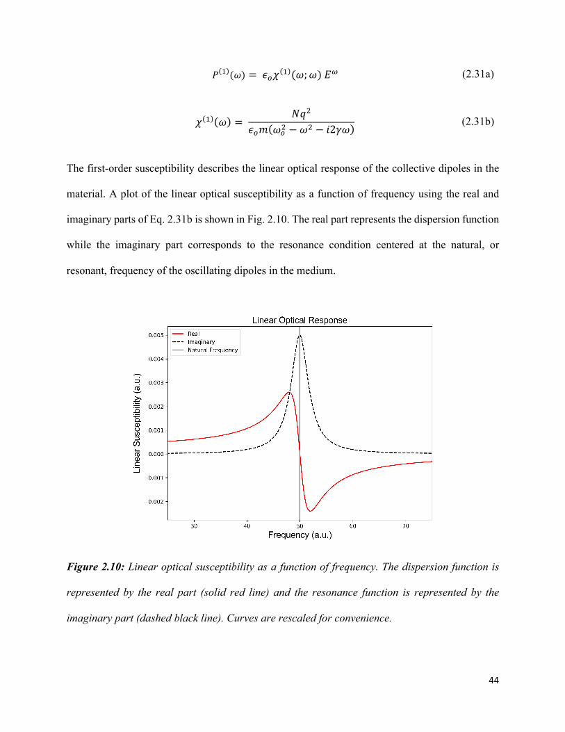
44
𝑃 1 (𝜔) = 𝜖$𝜒 a (𝜔;𝜔)𝐸 (2.31a)
𝜒 a 𝜔 = 𝑁𝑞b
𝜖$𝑚 𝜔$b − 𝜔b − 𝑖2𝛾𝜔 (2.31b)
The first-order susceptibility describes the linear optical response of the collective dipoles in the
material. A plot of the linear optical susceptibility as a function of frequency using the real and
imaginary parts of Eq. 2.31b is shown in Fig. 2.10. The real part represents the dispersion function
while the imaginary part corresponds to the resonance condition centered at the natural, or
resonant, frequency of the oscillating dipoles in the medium.
Figure 2.10: Linear optical susceptibility as a function of frequency. The dispersion function is
represented by the real part (solid red line) and the resonance function is represented by the
imaginary part (dashed black line). Curves are rescaled for convenience.

45
The linear response is only valid for optical fields which are too weak to generate higher-order
effects arising from nonlinearity in the electronic spring’s restoring force. In order to solve for the
second-order equation of motion, we may take the first-order solution from Eq. 2.29 and plug into
the second-order term of Eq. 2.28, dropping the 𝐸(𝑡) term, so that we have:
𝑑2𝑥(2)
𝑑𝑡2+ 2𝛾
𝑑𝑥(b)
𝑑𝑡 + 𝜔$b𝑥(b) +𝑎𝑚 𝑥(a) b = 0 (2.32)
In Eq. 2.32, ;�𝑥(a) b
serves as the excitation term and we are left to solve for the second-order
equation of motion from the following differential equation:
𝑑2𝑥(2)
𝑑𝑡2+ 2𝛾
𝑑𝑥(b)
𝑑𝑡 + 𝜔$b𝑥(b) = −𝑎𝑚 𝑥(a) b
(2.33a)
−𝑎𝑚 𝑥 a b = −
𝑎𝑞b
4𝑚b𝐸𝐸∗ + 𝐸∗𝐸
𝜔$b − 𝜔b b + 2𝛾𝜔 b −𝑎𝑞b
4𝑚b𝐸 b𝑒t6bE
𝜔$b − 𝜔b − 𝑖2𝛾𝜔 b
−𝑎𝑞b
4𝑚b𝐸∗ b𝑒6bE
𝜔$b − 𝜔b + 𝑖2𝛾𝜔 b
(2.33b)
The first term in Eq. 2.33b is an optical rectification term representing the establishment of an
optically induced electrostatic field in the medium. We may drop this term since it does not give
rise to a radiating dipole source. The second and third terms of Eq. 2.33b represent an electric field
oscillating at twice the frequency of the incident electric field. In order to obtain the time-
dependent second-order equation of motion, we input 𝑥 b 𝑡 = 𝐶𝑒t6bE + 𝐷𝑒6bE into Eq. 2.33a
to solve for the coefficients to find the second-order equation of motion as follows:

46
𝑥 b 𝑡 = −
𝑎𝑞b 𝐸 b𝑒t6bE
4𝑚b 𝜔$b − 4𝜔b − 𝑖4𝛾𝜔 𝜔$b − 𝜔b − 𝑖2𝛾𝜔 b
−𝑎𝑞b 𝐸∗ b𝑒6bE
4𝑚b 𝜔$b − 4𝜔b + 𝑖4𝛾𝜔 𝜔$b − 𝜔b + 𝑖2𝛾𝜔 b
(2.34)
Thus, we find the second-order polarization:
𝑃 b 𝑡 = −𝑁𝑞𝑥 b 𝑡 (2.35a)
𝑃 b 𝑡 =
𝑁𝑎𝑞c 𝐸 b𝑒t6bE
4𝑚b 𝜔$b − 4𝜔b − 𝑖4𝛾𝜔 𝜔$b − 𝜔b − 𝑖2𝛾𝜔 b
+𝑁𝑎𝑞c 𝐸∗ b𝑒6bE
4𝑚b 𝜔$b − 4𝜔b + 𝑖4𝛾𝜔 𝜔$b − 𝜔b + 𝑖2𝛾𝜔 b
(2.35b)
The resulting second-order polarization has the form, 𝑃 b 𝑡 = ab(𝑃 b (2𝜔)𝑒t6bE +
𝑃 b (2𝜔)∗𝑒6bE), where the second-order susceptibility can be pulled out from the second-order
polarization amplitude just like the first-order case:
𝑃 2 (2𝜔) = 𝜖$𝜒 b (2𝜔;𝜔,𝜔)𝐸𝐸 (2.36a)
𝜒 b 2𝜔;𝜔,𝜔 = 𝑁𝑎𝑞c
4𝜖$𝑚b 𝜔$b − 4𝜔b − 𝑖4𝛾𝜔 𝜔$b − 𝜔b − 𝑖2𝛾𝜔 b (2.36b)
The second-order susceptibility describes the nonlinear optical response of the collective dipoles
in the material. A plot of the nonlinear optical susceptibility as a function of frequency using the
real and imaginary parts of Eq. 2.36b is shown in Fig. 2.11.

47
Figure 2.11: Nonlinear optical susceptibility as a function of frequency. The dispersion function
is represented by the real part (solid red line) and the resonance function is represented by the
imaginary part (dashed black line). Curves and axes are rescaled for convenience.
The nonlinear susceptibility has two resonance frequencies, one when the fundamental frequency
of the incident light (𝜔) is equal to the natural dipole frequency (𝜔$) and one when the doubled-
frequency of the incident light (2𝜔) is equal to the natural dipole frequency. It is important to note
that the second-order response is expected to be at least ~1010-12 times weaker than the first-order
one [39]. Thus, we have illustrated the origin of optical nonlinearity using a simple classical
depiction of coulombic interactions in an atom.
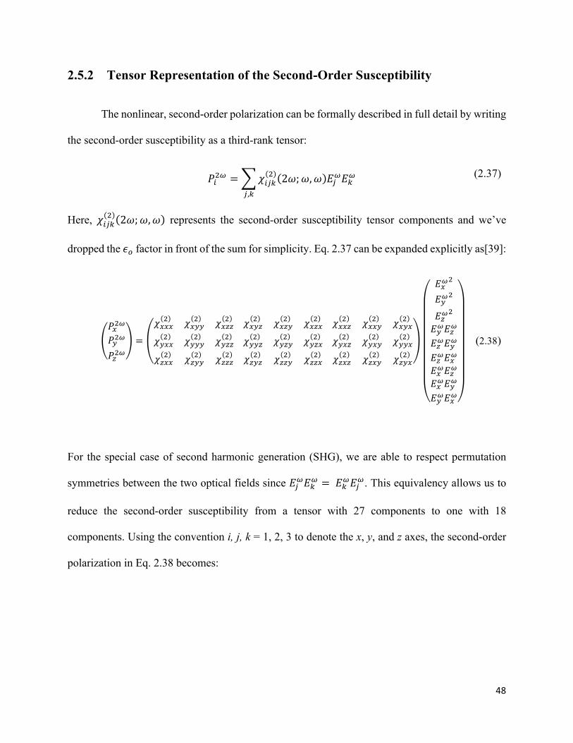
48
2.5.2 Tensor Representation of the Second-Order Susceptibility
The nonlinear, second-order polarization can be formally described in full detail by writing
the second-order susceptibility as a third-rank tensor:
𝑃6b = 𝜒6µ�b 2𝜔;𝜔,𝜔 𝐸µ𝐸�
µ,�
(2.37)
Here, 𝜒6µ�b 2𝜔;𝜔,𝜔 represents the second-order susceptibility tensor components and we’ve
dropped the 𝜖$ factor in front of the sum for simplicity. Eq. 2.37 can be expanded explicitly as[39]:
𝑃Hb
𝑃]b
𝑃Gb=
𝜒HHHb 𝜒H]]
b 𝜒HGGb
𝜒]HHb 𝜒]]]
b 𝜒]GGb
𝜒GHHb 𝜒G]]
b 𝜒GGGb
𝜒H]Gb 𝜒HG]
b 𝜒HGHb
𝜒]]Gb 𝜒]G]
b 𝜒]GHb
𝜒G]Gb 𝜒GG]
b 𝜒GGHb
𝜒HHGb 𝜒HH]
b 𝜒H]Hb
𝜒]HGb 𝜒]H]
b 𝜒]]Hb
𝜒GHGb 𝜒GH]
b 𝜒G]Hb
𝐸Hb
𝐸]b
𝐸Gb
𝐸]𝐸G
𝐸G𝐸]
𝐸G𝐸H𝐸H𝐸G𝐸H𝐸]
𝐸]𝐸H
(2.38)
For the special case of second harmonic generation (SHG), we are able to respect permutation
symmetries between the two optical fields since 𝐸µ𝐸� = 𝐸�𝐸µ. This equivalency allows us to
reduce the second-order susceptibility from a tensor with 27 components to one with 18
components. Using the convention i, j, k = 1, 2, 3 to denote the x, y, and z axes, the second-order
polarization in Eq. 2.38 becomes:

49
𝑃Hb
𝑃]b
𝑃Gb=
𝑑aa 𝑑ab 𝑑ac 𝑑ap 𝑑a¶ 𝑑a·𝑑ba 𝑑bb 𝑑bc 𝑑bp 𝑑b¶ 𝑑b·𝑑ca 𝑑cb 𝑑cc 𝑑cp 𝑑c¶ 𝑑c·
𝐸Hb
𝐸]b
𝐸Gb
2𝐸]𝐸G2𝐸H𝐸G2𝐸H𝐸]
(2.39)
For the above tensor equation, xx = 11 = 1, yy = 22 = 2, zz = 33 = 3, yz = 23 = 32 = 4, xz = 13 = 31
= 5, and xy = 12 = 21 = 6 [39, 40]. The non-vanishing components of the second-order
susceptibility hold all the significant structural information of the material being probed and are
determined according to the lattice symmetry, i.e. crystal point group symmetry. In order to obtain
any useful information about the material’s structure, or polar ordering, the SHG intensity must be
measured.
To derive the general expression for the SHG intensity, we start with Eq. 2.20 with the second-
order polarization acting as a source for radiation at the second-harmonic frequency:
∇× ∇×𝑬b(𝒓, 𝑡) +
𝑛b b
𝑐b𝜕b𝑬b(𝒓, 𝑡)
𝜕𝑡b = 𝜇$𝜕b𝑷b(𝒓, 𝑡)
𝜕𝑡b (2.40)
Let’s examine the case where the second-harmonic field is propagating along the z-axis inside a
nonlinear medium. The harmonic electrical and polarization fields can then be defined as follows:
𝑬b 𝒓, 𝑡 = 𝑬b 𝑧 𝑒t𝒊 bE (2.41)
𝑷b 𝒓, 𝑡 = 𝑷b 𝑧 𝑒t𝒊 bE (2.42)

50
Plugging these fields into the wave equation and carrying out time-derivatives leaves us with a
spatially-resolved wave equation in terms of the amplitude functions:
−∇× ∇×𝑬b 𝑧 +
𝑛b b 2𝜔 b
𝑐b 𝑬b(𝑧) = 𝜇$ 2𝜔 b𝑷b(𝑧) (2.43)
Since we are considering a unidirectional propagation along the z-axis, the following
approximation for the curl term can be made [39, 88]:
−∇× ∇×𝑬b 𝑧 =
𝜕b𝑬b 𝑧𝜕𝑧b + 2𝑖𝑘b
𝜕𝑬b 𝑧𝜕𝑧 − 𝑘b b𝑬b 𝑧
(2.44)
Since the change in amplitude of the second-harmonic field over the length of a wavelength is
negligible, the slowly-varying amplitude approximation can be used to simplify Eq. 2.44 by
dropping the second-order derivative with respect to z. Thus, Eq. 2.43 becomes:
2𝑖𝑘b
𝜕𝑬b 𝑧𝜕𝑧 − 𝑘b b𝑬b 𝑧 +
𝑛b b 2𝜔 b
𝑐b 𝑬b(𝑧) = 𝜇$ 2𝜔 b𝑷b(𝑧) (2.43)
The second and third terms on the left-hand side cancel out because 𝑘b = b∙�ª¹
S. We are left
with:
2𝑖𝑘b
𝜕𝑬b 𝑧𝜕𝑧 = 𝜇$ 2𝜔 b𝑷b(𝑧)
(2.45)
We now can make the substitution for the amplitude functions of the second-harmonic electric and
polarization fields:
51
𝑬b 𝑧 = 𝐸b 𝑧 𝑒𝒊 𝑘2𝜔𝑧 (2.46)
𝑷b 𝑧 = 2𝜖$𝜒[))(b) 𝐸 b𝑒6 2𝑘𝜔𝑧 (2.47)
In Eq. 2.47, 𝜒[))(b) is the effective second-order susceptibility which takes into account polarization
directional vectors as well as Fresnel transformation factors for the single-frequency electric fields.
Then Eq. 2.45 can be rearranged into the following differential equation:
𝜕𝐸b 𝑧𝜕𝑧 =
−𝑖𝜔𝑛2𝜔𝑐
𝜒[))(b) 𝐸 b𝑒6 Δ𝑘𝑧
(2.48)
In Eq. 2.48, Δ𝑘 = 2𝑘 − 𝑘b. Integrating with respect to z over the interaction length, L, and
solving for the second-harmonic optical intensity finally leaves us with:
𝐼b =
2𝜔b 𝜒[))(b) b
𝐿b𝑛2𝜔 𝑛𝜔 2𝑐3𝜖𝑜
𝑠𝑖𝑛 Δ𝑘𝐿/2Δ𝑘𝐿/2
b
𝐼b b (2.49)
The result in Eq. 2.49 shows that the functional form of the SHG intensity depends directly
on the structural symmetry of the probed region, while the magnitude of the SHG intensity scales
with the square of the incident optical intensity. In practice, the SHG intensity profile may be fitted
according to the proportionality, 𝐼b ∝ 𝜒[))(b) b
or 𝐼b ∝ 𝑃b b depending on the system being
studied. Various factors, such as refraction, sample orientation, and optical polarization axes, must

52
be taken into consideration to properly analyze information about the structure and/or polar
ordering of the material, which will be discussed as needed in later chapters.
2.5.3 SHG Phase-Matching
A very significant phase-matching condition becomes apparent as a result of the sinc
functional term present in the expression. Firstly, Eq. 2.49 was derived under the assumption that
the SHG conversion efficiency is low and that the incident fundamental light does not deplete as
it travels through the nonlinear medium. Secondly, the sinc term limits the SHG intensity unless
the argument, Δ𝑘𝐿/2, is equal to zero. This means that for very efficient SHG conversion, we want
Δ𝑘 = 2𝑘 − 𝑘b = 0, or 𝑛b = 𝑛. This is typically not the case and many materials
demonstrate 𝑛b > 𝑛. Thus, the depth in a material from which second-harmonic light can be
generated is limited by what’s known as the SHG coherence length. This is the distance that SHG
light can travel before destructively interfering with itself. As a result, it does not pay off to use
nonlinear materials thicker than the coherence length since SHG light is limited to this depth. To
illustrate the coherence length, we may plot the sinc function, as shown in Fig. 2.12.
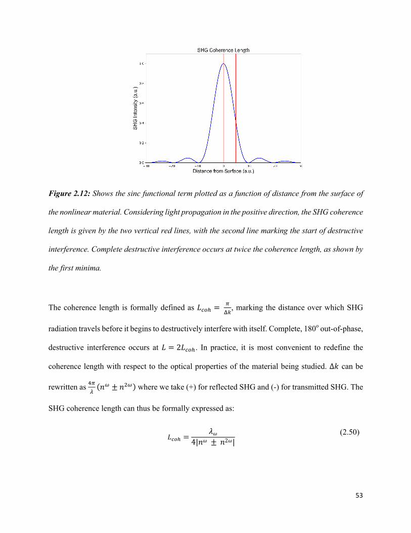
53
Figure 2.12: Shows the sinc functional term plotted as a function of distance from the surface of
the nonlinear material. Considering light propagation in the positive direction, the SHG coherence
length is given by the two vertical red lines, with the second line marking the start of destructive
interference. Complete destructive interference occurs at twice the coherence length, as shown by
the first minima.
The coherence length is formally defined as 𝐿S$} = ÀÁ�
, marking the distance over which SHG
radiation travels before it begins to destructively interfere with itself. Complete, 180o out-of-phase,
destructive interference occurs at 𝐿 = 2𝐿S$}. In practice, it is most convenient to redefine the
coherence length with respect to the optical properties of the material being studied. Δ𝑘 can be
rewritten as pÀÂ𝑛 ± 𝑛b where we take (+) for reflected SHG and (-) for transmitted SHG. The
SHG coherence length can thus be formally expressed as:
𝐿S$} =𝜆𝜔
4|𝑛𝜔 ±𝑛2𝜔| (2.50)

54
It becomes clear that the coherence length has a dependence on the refractive indices of the
material (𝑛 and 𝑛b) as well as the wavelength of the fundamental laser light (𝜆) used to induce
a nonlinear response. Further experimental details about the SHG coherence length in STO and
BTO are given in the next chapter.
55
Chapter 3: Experimental Details
This chapter presents details of sample preparation and experimental methods used for
second harmonic generation, confocal Raman, and fluorescence measurements. In section 3.1,
descriptions regarding the preparation of Fe-doped SrTiO3 single crystals and ferroelectric Zr-
doped BaTiO3 thick films are given. Section 3.2 goes over the femtosecond laser systems used for
second harmonic generation measurements. Section 3.3 discusses polarization-resolved second
harmonic generation measurements. Section 3.4 and 3.5 give brief descriptions for the collection
of confocal Raman and steady-state fluorescence spectra.
3.1 Samples
3.1.1 Fe:STO Single Crystals
(100) SrTiO3 single crystals doped with 0.01 wt.% Fe (Fe:STO) were purchased from MTI
corporation (Richmond, CA) and cut into 5 x 5 x 0.5 mm3 pieces and epi-polished on both 5 x 5
mm2 faces. The Fe:STO single crystals were then annealed in a tube furnace at 900°C under a
partial oxygen pressures of 2x10⁻⁵ bar and 0.2 bar for reduction and oxidation treatment,
respectively. Reduced crystals were then quenched in argon and oxidized crystals were quenched
in air at 25oC to freeze-in ionic defect concentrations ([Fe]tot ~ 5.58 x 10¹⁸/cm3). Calculated defect
concentrations [𝑉k∙∙], [Fe3+], and [Fe4+] based on mass action constants are given in Table 3.1[51].
Reduced crystals have larger concentrations of Fe3+ and oxygen vacancies while oxidized crystals
have larger concentrations of Fe4+ and oxygen. Electrochemically reduced and oxidized crystals
enabled comparative analyses based on oxygen vacancy concentrations.
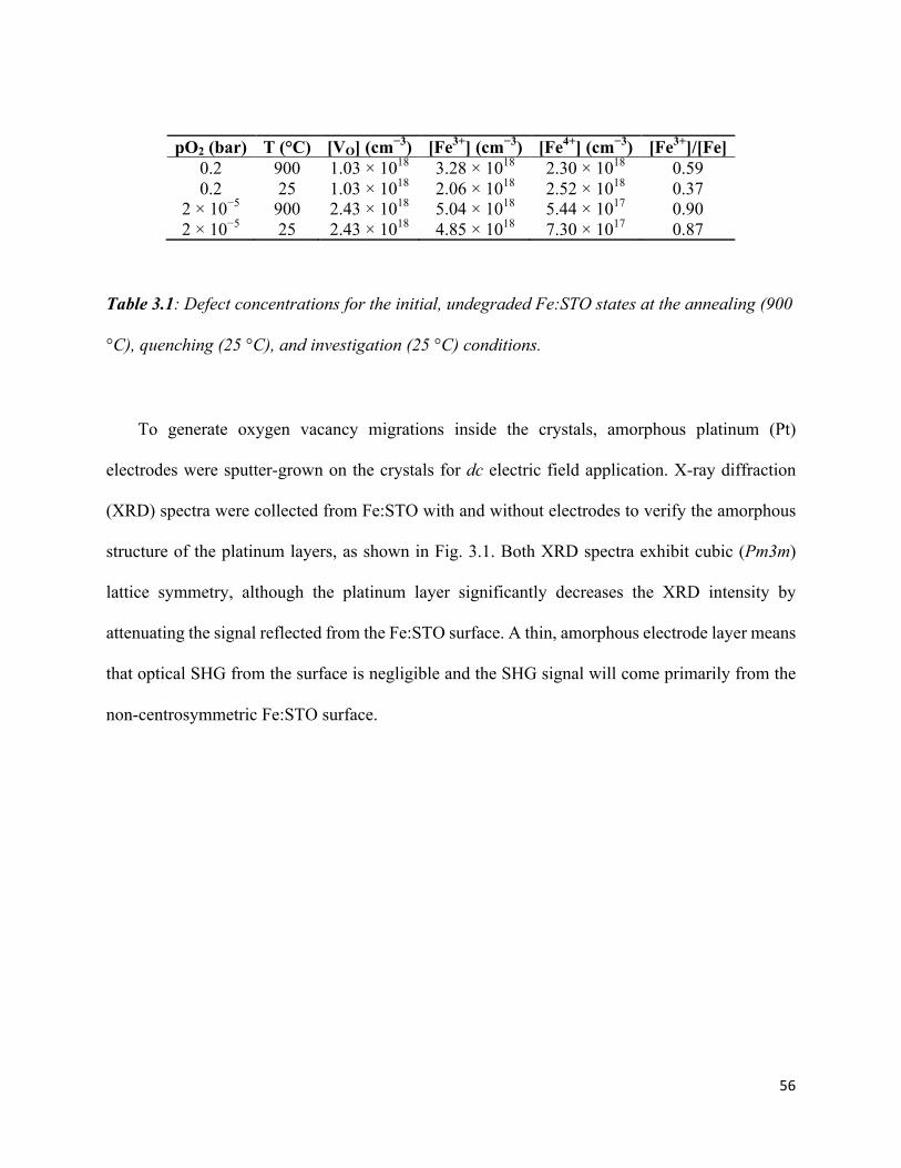
56
pO2 (bar) T (°C) [VO] (cm−3) [Fe3+] (cm−3) [Fe4+] (cm−3) [Fe3+]/[Fe] 0.2 900 1.03 × 10¹⁸ 3.28 × 10¹⁸ 2.30 × 10¹⁸ 0.59 0.2 25 1.03 × 10¹⁸ 2.06 × 10¹⁸ 2.52 × 10¹⁸ 0.37
2 × 10⁻⁵ 900 2.43 × 10¹⁸ 5.04 × 10¹⁸ 5.44 × 10¹⁷ 0.90 2 × 10⁻⁵ 25 2.43 × 10¹⁸ 4.85 × 10¹⁸ 7.30 × 10¹⁷ 0.87
Table 3.1: Defect concentrations for the initial, undegraded Fe:STO states at the annealing (900
°C), quenching (25 °C), and investigation (25 °C) conditions.
To generate oxygen vacancy migrations inside the crystals, amorphous platinum (Pt)
electrodes were sputter-grown on the crystals for dc electric field application. X-ray diffraction
(XRD) spectra were collected from Fe:STO with and without electrodes to verify the amorphous
structure of the platinum layers, as shown in Fig. 3.1. Both XRD spectra exhibit cubic (Pm3m)
lattice symmetry, although the platinum layer significantly decreases the XRD intensity by
attenuating the signal reflected from the Fe:STO surface. A thin, amorphous electrode layer means
that optical SHG from the surface is negligible and the SHG signal will come primarily from the
non-centrosymmetric Fe:STO surface.
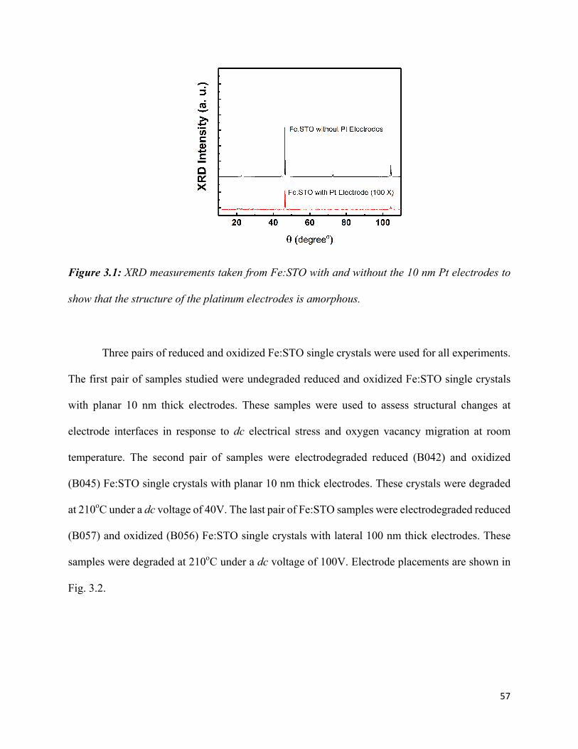
57
Figure 3.1: XRD measurements taken from Fe:STO with and without the 10 nm Pt electrodes to
show that the structure of the platinum electrodes is amorphous.
Three pairs of reduced and oxidized Fe:STO single crystals were used for all experiments.
The first pair of samples studied were undegraded reduced and oxidized Fe:STO single crystals
with planar 10 nm thick electrodes. These samples were used to assess structural changes at
electrode interfaces in response to dc electrical stress and oxygen vacancy migration at room
temperature. The second pair of samples were electrodegraded reduced (B042) and oxidized
(B045) Fe:STO single crystals with planar 10 nm thick electrodes. These crystals were degraded
at 210oC under a dc voltage of 40V. The last pair of Fe:STO samples were electrodegraded reduced
(B057) and oxidized (B056) Fe:STO single crystals with lateral 100 nm thick electrodes. These
samples were degraded at 210oC under a dc voltage of 100V. Electrode placements are shown in
Fig. 3.2.
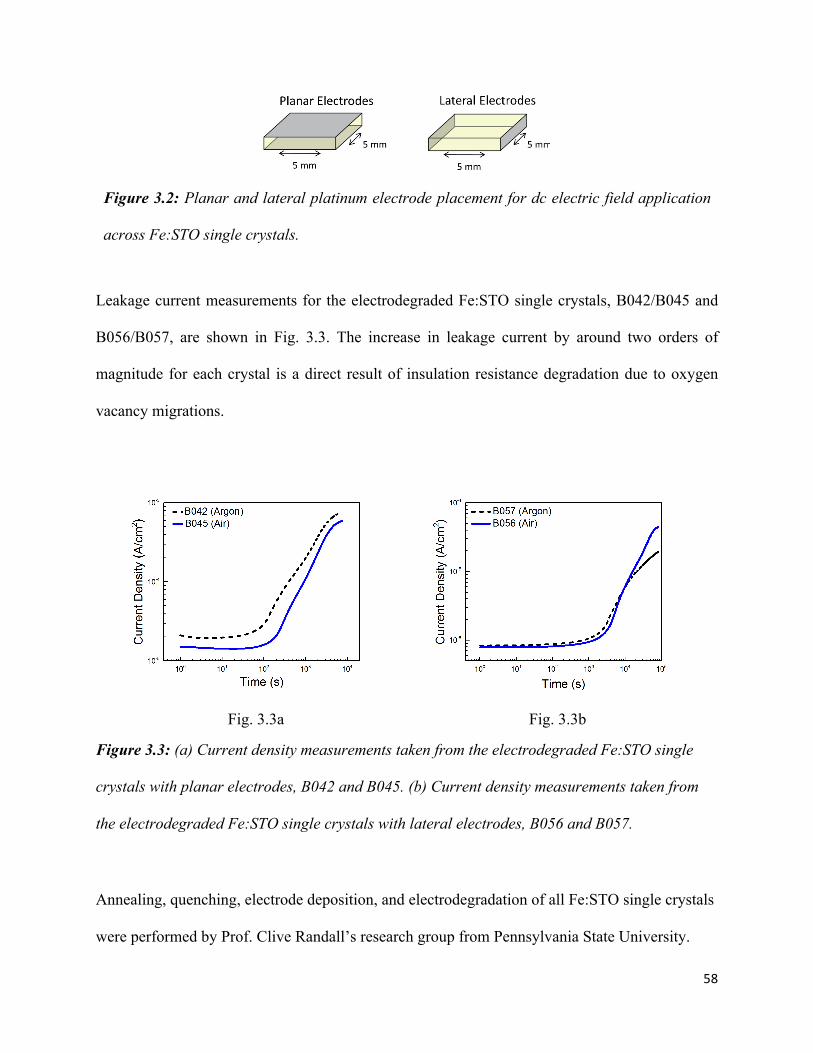
58
Figure 3.2: Planar and lateral platinum electrode placement for dc electric field application
across Fe:STO single crystals.
Leakage current measurements for the electrodegraded Fe:STO single crystals, B042/B045 and
B056/B057, are shown in Fig. 3.3. The increase in leakage current by around two orders of
magnitude for each crystal is a direct result of insulation resistance degradation due to oxygen
vacancy migrations.
Fig. 3.3a Fig. 3.3b
Figure 3.3: (a) Current density measurements taken from the electrodegraded Fe:STO single
crystals with planar electrodes, B042 and B045. (b) Current density measurements taken from
the electrodegraded Fe:STO single crystals with lateral electrodes, B056 and B057.
Annealing, quenching, electrode deposition, and electrodegradation of all Fe:STO single crystals
were performed by Prof. Clive Randall’s research group from Pennsylvania State University.

59
3.1.2 BZT Films
LaAlO3 (LAO), (La,Sr)(Al,Ta)O3 (LSAT), and SrTiO3 (STO) substrates with dimensions
of 10 x 10 x 0.5 mm3 and SrRuO3 (SRO) ceramic targets (Φ = 50 mm, t = 5 mm, 3N purity) were
provided by the Anhui Institute of Optics and Fine Mechanics of the Chinese Academy of
Sciences. Ba(Zr0.2Ti0.8)O3 (BZT) ceramic targets were prepared using a solid solution-based
reaction by Prof. Jun Ouyang’s research group from Shandong University. Titanium oxide (TiO2,
98%), zirconium oxide (ZrO2, 99%), and barium carbonate (BaCO3, 99%) powders were used as
primary reagents. Details on the ceramic sintering process are discussed elsewhere[79]. RF-
magnetron sputtering, with a base chamber pressure of 2.0×10⁻⁹ bar (2.0×10⁻⁴ Pa), was used for
the deposition of ~100 nm SRO electrode layers on the top of each substrate followed by the
epitaxial growth of ferroelectric BZT thick films. Lastly, circular gold (Au) electrodes (Φ = 200
µm) were sputtered on the BZT films at room temperature using a shadow mask. An SEM side
profile of a typical Au plated surface, ferroelectric BZT film, SRO electrode, and perovskite oxide
substrate structure is shown in Fig. 3.4.
Figure 3.4: Shows the typical sequential structure for the ferroelectric thick films studied in this
work. Circular Au electrodes are spread across the BZT surface. Beneath the bulk layers of the
BZT film lies the SRO electrode layer over the surface of the perovskite oxide substrate.
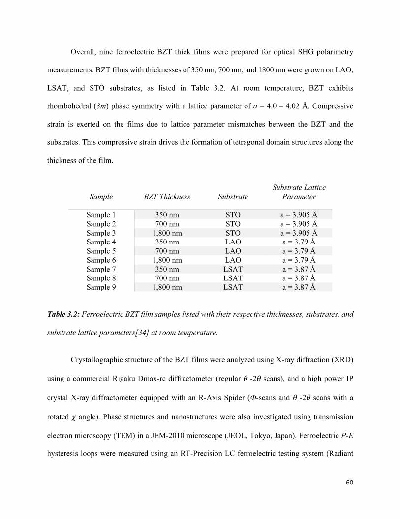
60
Overall, nine ferroelectric BZT thick films were prepared for optical SHG polarimetry
measurements. BZT films with thicknesses of 350 nm, 700 nm, and 1800 nm were grown on LAO,
LSAT, and STO substrates, as listed in Table 3.2. At room temperature, BZT exhibits
rhombohedral (3m) phase symmetry with a lattice parameter of a = 4.0 – 4.02 Å. Compressive
strain is exerted on the films due to lattice parameter mismatches between the BZT and the
substrates. This compressive strain drives the formation of tetragonal domain structures along the
thickness of the film.
Sample BZT Thickness Substrate Substrate Lattice
Parameter
Sample 1 350 nm STO a = 3.905 Å Sample 2 700 nm STO a = 3.905 Å Sample 3 1,800 nm STO a = 3.905 Å Sample 4 350 nm LAO a = 3.79 Å Sample 5 700 nm LAO a = 3.79 Å Sample 6 1,800 nm LAO a = 3.79 Å Sample 7 350 nm LSAT a = 3.87 Å Sample 8 700 nm LSAT a = 3.87 Å Sample 9 1,800 nm LSAT a = 3.87 Å
Table 3.2: Ferroelectric BZT film samples listed with their respective thicknesses, substrates, and
substrate lattice parameters[34] at room temperature.
Crystallographic structure of the BZT films were analyzed using X-ray diffraction (XRD)
using a commercial Rigaku Dmax-rc diffractometer (regular q -2q scans), and a high power IP
crystal X-ray diffractometer equipped with an R-Axis Spider (F-scans and q -2q scans with a
rotated c angle). Phase structures and nanostructures were also investigated using transmission
electron microscopy (TEM) in a JEM-2010 microscope (JEOL, Tokyo, Japan). Ferroelectric P-E
hysteresis loops were measured using an RT-Precision LC ferroelectric testing system (Radiant

61
Technology, NM, USA), and the dielectric properties (C-f, C-V) were measured with a high
precision digital bridge (LCR meter, QuadTech 7600plus) and an Agilent1505A power device
analyzer (by applying a 50 mV, 5 kHz ac signal and sweeping a dc bias voltage from a negative
to positive maximum value). Temperature-dependent measurements were taken using a
temperature-controlled probe station (Linkam-HFS600E-PB2). Characterization of dielectric
properties and measurement of ferroelectric hysteresis curves were performed by Dr. Jun Ouyang’s
research group from Shandong University.
3.2 Femtosecond Laser Systems
As a nonlinear optical process, SHG requires high power light sources to take place.
Although only milliwatt-range power is needed to induce a nonlinear response from a non-
centrosymmetric medium, a significantly high amount of energy is required to produce high
intensity laser fields using continuous wave (CW) lasers. Thus, pulsed laser systems are essential
components for probing nonlinear structure in crystalline solids using SHG. Two femtosecond
laser systems were used in this experimental work, a Ti:Sapphire (Ti:Al2O3) oscillator (Tsunami,
Spectra-physics) and a Ti:Sapphire regenerative amplifier (RegA 9000, Coherent).
3.2.1 Mode-locked Ti:Sapphire Oscillator
Our primary femtosecond pulsed laser system consists of a Diode-Pumped Frequency-
Doubled CW-Nd:Vanadate Laser (Millennia Pro, Spectra-Physics) and a Broadband Tunable
Ti:Sapphire Oscillator (Tsunami, Spectra-Physics). A schematic for the mode-locked Ti:Sapphire
oscillator is shown in Fig. 3.5.
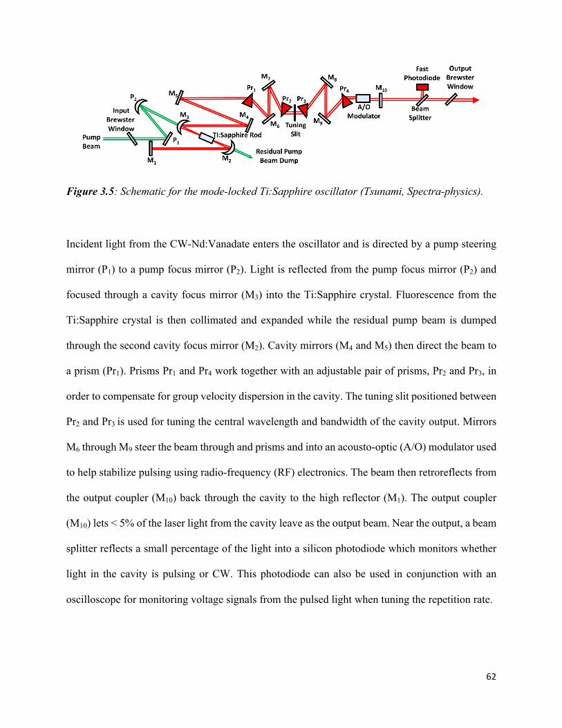
62
Figure 3.5: Schematic for the mode-locked Ti:Sapphire oscillator (Tsunami, Spectra-physics).
Incident light from the CW-Nd:Vanadate enters the oscillator and is directed by a pump steering
mirror (P1) to a pump focus mirror (P2). Light is reflected from the pump focus mirror (P2) and
focused through a cavity focus mirror (M3) into the Ti:Sapphire crystal. Fluorescence from the
Ti:Sapphire crystal is then collimated and expanded while the residual pump beam is dumped
through the second cavity focus mirror (M2). Cavity mirrors (M4 and M5) then direct the beam to
a prism (Pr1). Prisms Pr1 and Pr4 work together with an adjustable pair of prisms, Pr2 and Pr3, in
order to compensate for group velocity dispersion in the cavity. The tuning slit positioned between
Pr2 and Pr3 is used for tuning the central wavelength and bandwidth of the cavity output. Mirrors
M6 through M9 steer the beam through and prisms and into an acousto-optic (A/O) modulator used
to help stabilize pulsing using radio-frequency (RF) electronics. The beam then retroreflects from
the output coupler (M10) back through the cavity to the high reflector (M1). The output coupler
(M10) lets < 5% of the laser light from the cavity leave as the output beam. Near the output, a beam
splitter reflects a small percentage of the light into a silicon photodiode which monitors whether
light in the cavity is pulsing or CW. This photodiode can also be used in conjunction with an
oscilloscope for monitoring voltage signals from the pulsed light when tuning the repetition rate.

63
The alignment of the laser beam within the resonant cavity is critical for the generation of
infrared pulsed light. The pump beam entering the oscillator from the CW-Nd:Vanadate Laser
(Millenia Pro, Spectra-physics) must be collinear with the cavity mode over the Ti:Sapphire rod.
This is done so by overlapping beam paths of the pump light and the fluorescence light from the
Ti:Sapphire crystal. To optimize mode-locking within the cavity, the prism system is used to
control dispersion compensation. Micrometers on the exterior of the Ti:Sapphire oscillator body
allow the user to tune the heights of prisms Pr2 and Pr3. These prism heights must be tuned until
the laser’s output bandwidth expands to a maximum. Next, the vertical and horizontal axes of the
end mirrors, M1 and M10 can be adjusted to optimize the output power. Once the system is pulsing
with an optimized output power of ~780 – 800 mW, it is best to only adjust M1 for power tuning
during day-to-day operation to avoid walking the output beam path over time. It is crucial that the
output power be adjusted while monitoring the output spectrum to make sure the laser is stable
and pulsing.
The generation of laser pulses in the oscillator is due to a very important principle known
as mode-locking. In a laser cavity, a standing wave is formed when propagating light waves
constructively interfere with each other at fixed positions along the beam path. Optical
wavelengths which satisfy this condition are known as the longitudinal modes of the laser cavity.
As a simplification, consider light reflecting back and forth between the end mirrors, M1 and M10,
of the optical cavity. By using the wave equation, we may solve for the longitudinal modes:
∇b𝐸 𝑧, 𝑡 −
1𝑐b𝜕b𝐸 𝑧, 𝑡𝜕𝑡b = 0
(3.1)
64
Our boundary conditions are 𝐸 𝑧 = 0, 𝑡 = 0 and 𝐸 𝑧 = 𝐿, 𝑡 = 0 where L represents the cavity
length as the distance between end mirrors along the z-axis. Using separation of variables, we may
write the electric field as 𝐸 𝑧, 𝑡 = 𝑍 𝑧 𝑇(𝑡), such that Eq. 3.1 becomes:
𝑍ÆÆ 𝑧 𝑇(𝑡) −1𝑐b 𝑍(𝑧)𝑇′′(𝑡) = 0
(3.2)
Dividing through by 𝑍 𝑧 𝑇(𝑡) gives us the following equations:
𝑍ÆÆ 𝑧𝑍(𝑧) −
1𝑐b𝑇′′(𝑡)𝑇(𝑡) = 0
(3.2)
−𝑘b +
𝜔b
𝑐b = 0 (3.3)
Thus, Eq. 3.1 becomes two separate ordinary differential equations which we can solve for without
much difficulty:
𝑍ÆÆ 𝑧 = −𝑘b𝑍(𝑧) (3.4)
𝑇ÆÆ 𝑡 = −
𝜔𝑐
b𝑍(𝑧)
(3.5)
General solutions for Eq. 3.4 and Eq. 3.5 are 𝑍 𝑧 = 𝐴𝑠𝑖𝑛 𝑘𝑧 + 𝐵𝑐𝑜𝑠(𝑘𝑧) and 𝑇 𝑡 =
𝐶𝑒t6¹WE + 𝐷𝑒6
¹WE , respectively. To satisfy the first boundary condition, we must have 𝑍 0 =
𝐴𝑠𝑖𝑛 0 + 𝐵𝑐𝑜𝑠 0 = 0, so coefficient B has to be 0. To satisfy the second condition, 𝑍 𝐿 =
𝐴𝑠𝑖𝑛 𝑘𝐿 can only be 0 if 𝑘𝐿 = 𝑛𝜋. Thus, 𝑘 = �À1
and we obtain a dispersion relation for the
longitudinal modes of the system using Eq. 3.3:
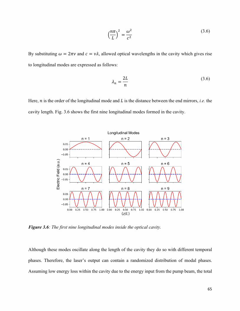
65
𝑛𝜋𝐿
b=𝜔b
𝑐b (3.6)
By substituting 𝜔 = 2𝜋𝜈 and 𝑐 = 𝜈𝜆, allowed optical wavelengths in the cavity which gives rise
to longitudinal modes are expressed as follows:
𝜆� =2𝐿𝑛
(3.6)
Here, 𝑛 is the order of the longitudinal mode and 𝐿 is the distance between the end mirrors, i.e. the
cavity length. Fig. 3.6 shows the first nine longitudinal modes formed in the cavity.
Figure 3.6: The first nine longitudinal modes inside the optical cavity.
Although these modes oscillate along the length of the cavity they do so with different temporal
phases. Therefore, the laser’s output can contain a randomized distribution of modal phases.
Assuming low energy loss within the cavity due to the energy input from the pump beam, the total

66
electric field in the cavity, which is a vector sum of all longitudinal modes, can be expressed as
the following Fourier series:
𝐸 𝑧, 𝑡 = 𝐸�sin𝑛𝜋𝑧𝐿 cos
𝑛𝜋𝑡𝐿 + 𝜙�(𝑡)
�
(3.7)
In Eq. 3.7, n represents the longitudinal mode order and L represents the effective cavity length.
𝜙�(𝑡) represents a phase term that can be associated with each longitudinal mode. The total electric
field propagating within the cavity is shown in Fig. 3.8a. Intensities, which are given by 𝐼 ∝ 𝐸 b,
are shown in Fig. 3.7b.
Fig. 3.7a Fig. 3.7b
Figure 3.7: (a) Cumulative electric field in the cavity calculated from summing the first 30
longitudinal modes. The electric field is shown propagating left to right over time. (b) Pulse
intensity traveling to the right. A pulse leaves the output coupler each cycle.
The pulse train leaving the output coupler consists of 100 fs long pulses exiting the cavity
at a repetition rate of 80 MHz with an average energy of about 10 nJ/pulse. One cycle has a duration
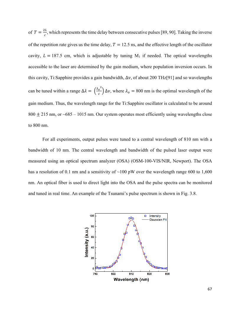
67
of 𝑇 = b1S
, which represents the time delay between consecutive pulses [89, 90]. Taking the inverse
of the repetition rate gives us the time delay, 𝑇 =12.5 ns, and the effective length of the oscillator
cavity, 𝐿 =187.5 cm, which is adjustable by tuning M1 if needed. The optical wavelengths
accessible to the laser are determined by the gain medium, where population inversion occurs. In
this cavity, Ti:Sapphire provides a gain bandwidth, ∆𝜈, of about 200 THz[91] and so wavelengths
can be tuned within a range Δ𝜆 = Â|ª
S∆𝜈, where 𝜆$ = 800 nm is the optimal wavelength of the
gain medium. Thus, the wavelength range for the Ti:Sapphire oscillator is calculated to be around
800 ±215 nm, or ~685 – 1015 nm. Our system operates most efficiently using wavelengths close
to 800 nm.
For all experiments, output pulses were tuned to a central wavelength of 810 nm with a
bandwidth of 10 nm. The central wavelength and bandwidth of the pulsed laser output were
measured using an optical spectrum analyzer (OSA) (OSM-100-VIS/NIR, Newport). The OSA
has a resolution of 0.1 nm and a sensitivity of ~100 pW over the wavelength range 600 to 1,600
nm. An optical fiber is used to direct light into the OSA and the pulse spectra can be monitored
and tuned in real time. An example of the Tsunami’s pulse spectrum is shown in Fig. 3.8.
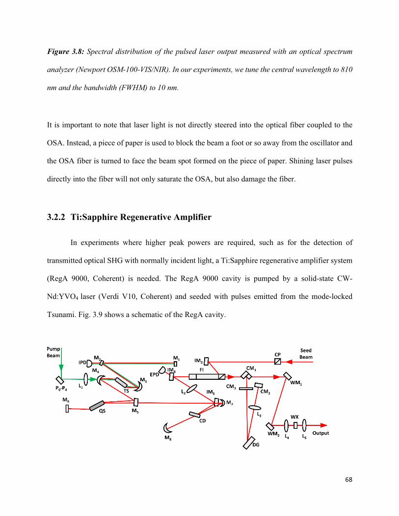
68
Figure 3.8: Spectral distribution of the pulsed laser output measured with an optical spectrum
analyzer (Newport OSM-100-VIS/NIR). In our experiments, we tune the central wavelength to 810
nm and the bandwidth (FWHM) to 10 nm.
It is important to note that laser light is not directly steered into the optical fiber coupled to the
OSA. Instead, a piece of paper is used to block the beam a foot or so away from the oscillator and
the OSA fiber is turned to face the beam spot formed on the piece of paper. Shining laser pulses
directly into the fiber will not only saturate the OSA, but also damage the fiber.
3.2.2 Ti:Sapphire Regenerative Amplifier
In experiments where higher peak powers are required, such as for the detection of
transmitted optical SHG with normally incident light, a Ti:Sapphire regenerative amplifier system
(RegA 9000, Coherent) is needed. The RegA 9000 cavity is pumped by a solid-state CW-
Nd:YVO4 laser (Verdi V10, Coherent) and seeded with pulses emitted from the mode-locked
Tsunami. Fig. 3.9 shows a schematic of the RegA cavity.

69
Figure 3.9: A schematic of the Ti:Sapphire regenerative amplifier system (RegA 9000, Coherent).
The Ti:Sapphire regenerative amplifier is used to amplify the peak power of femtosecond pulses
from the Ti:Sapphire oscillator. CW light (10 W) from the ND:YVO4 laser enters the Ti:Sapphire
RegA as the pump beam (shown in green in Fig. 3.9). The pump beam is directed through the
pump optics mirrors (P0-P4) and passed through focused (L1) on a Ti:Sapphire crystal (TS). 100 fs
pulses from the Tsunami are fed into the Ti:Sapphire RegA as the seed beam, passing through a
polarizer (CP) and reflecting off of a mirror (IM4) into a Faraday Isolator (FI) which is used to
prevent pulses from reflecting backwards into the Tsunami. Tsunami pulses are injected into the
RegA cavity (cavity length between M1 and M8) with a tellurium dioxide (TeO2) acousto-optic
cavity dumper (CD). Amplification inside the RegA cavity occurs over ~25 roundtrips and allows
the dispersion taking place in a TeO2 Q-switch (QS) to expand the 100 fs pulses to 40 ps pulses.
This so-called pulse stretching step is necessary for safe energy extraction from the laser pulses,
otherwise catastrophic damage can be inflicted on the cavity optics. Once pulses are stretched, the
cavity dumper (CD) extracts a pulse of several µJ in energy. The accumulated chirp acquired by
pulses during amplification is canceled out using a single holographic diffraction grating (DG)
which compresses pulses to ~200 fs pulse widths for the RegA output. Thus, the pulse train leaving
the output consists of 200 fs long pulses exiting the cavity at a repetition rate of 250 kHz with an
average energy of about 5 µJ /pulse.
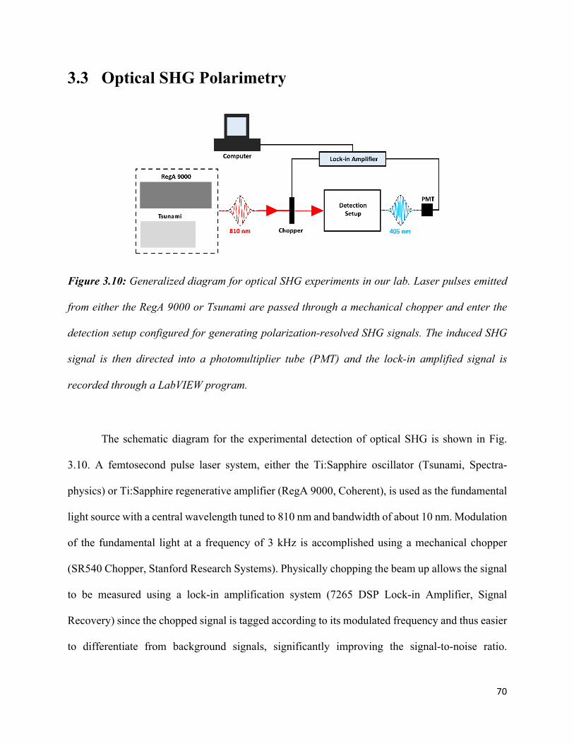
70
3.3 Optical SHG Polarimetry
Figure 3.10: Generalized diagram for optical SHG experiments in our lab. Laser pulses emitted
from either the RegA 9000 or Tsunami are passed through a mechanical chopper and enter the
detection setup configured for generating polarization-resolved SHG signals. The induced SHG
signal is then directed into a photomultiplier tube (PMT) and the lock-in amplified signal is
recorded through a LabVIEW program.
The schematic diagram for the experimental detection of optical SHG is shown in Fig.
3.10. A femtosecond pulse laser system, either the Ti:Sapphire oscillator (Tsunami, Spectra-
physics) or Ti:Sapphire regenerative amplifier (RegA 9000, Coherent), is used as the fundamental
light source with a central wavelength tuned to 810 nm and bandwidth of about 10 nm. Modulation
of the fundamental light at a frequency of 3 kHz is accomplished using a mechanical chopper
(SR540 Chopper, Stanford Research Systems). Physically chopping the beam up allows the signal
to be measured using a lock-in amplification system (7265 DSP Lock-in Amplifier, Signal
Recovery) since the chopped signal is tagged according to its modulated frequency and thus easier
to differentiate from background signals, significantly improving the signal-to-noise ratio.
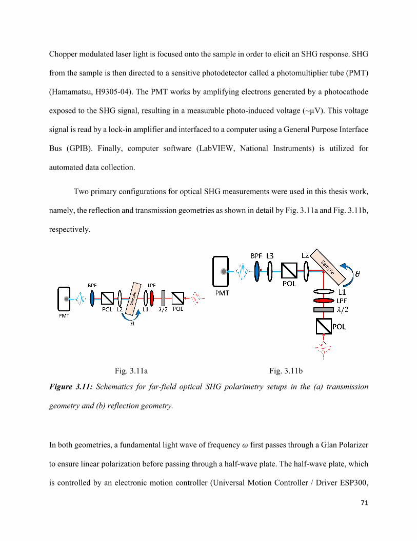
71
Chopper modulated laser light is focused onto the sample in order to elicit an SHG response. SHG
from the sample is then directed to a sensitive photodetector called a photomultiplier tube (PMT)
(Hamamatsu, H9305-04). The PMT works by amplifying electrons generated by a photocathode
exposed to the SHG signal, resulting in a measurable photo-induced voltage (~µV). This voltage
signal is read by a lock-in amplifier and interfaced to a computer using a General Purpose Interface
Bus (GPIB). Finally, computer software (LabVIEW, National Instruments) is utilized for
automated data collection.
Two primary configurations for optical SHG measurements were used in this thesis work,
namely, the reflection and transmission geometries as shown in detail by Fig. 3.11a and Fig. 3.11b,
respectively.
Fig. 3.11a Fig. 3.11b
Figure 3.11: Schematics for far-field optical SHG polarimetry setups in the (a) transmission
geometry and (b) reflection geometry.
In both geometries, a fundamental light wave of frequency 𝜔 first passes through a Glan Polarizer
to ensure linear polarization before passing through a half-wave plate. The half-wave plate, which
is controlled by an electronic motion controller (Universal Motion Controller / Driver ESP300,
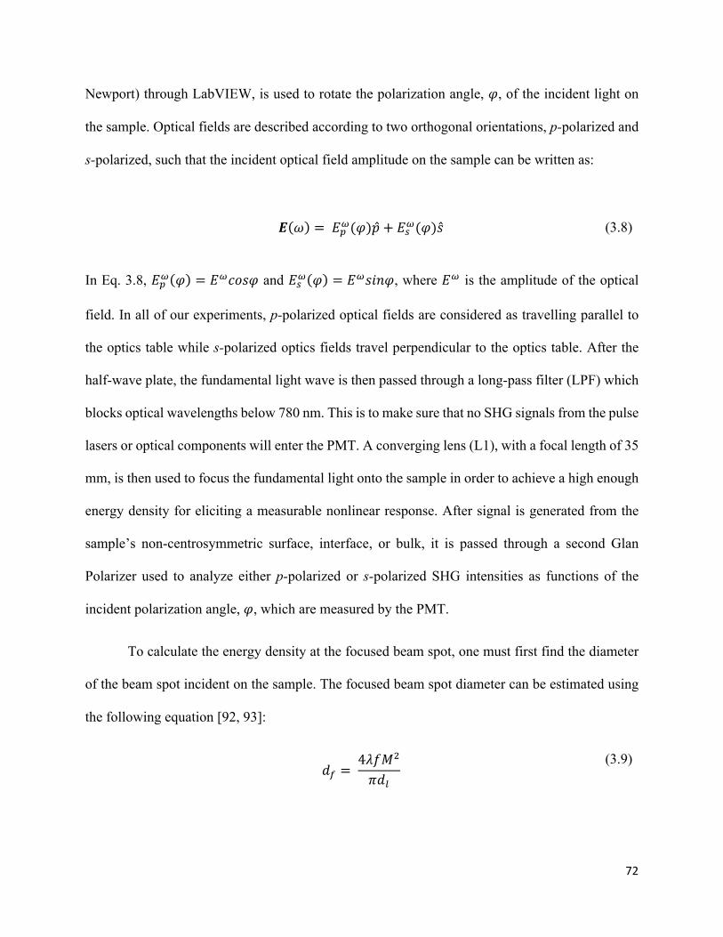
72
Newport) through LabVIEW, is used to rotate the polarization angle, 𝜑, of the incident light on
the sample. Optical fields are described according to two orthogonal orientations, p-polarized and
s-polarized, such that the incident optical field amplitude on the sample can be written as:
𝑬 𝜔 =𝐸<(𝜑)𝑝 + 𝐸%(𝜑)𝑠 (3.8)
In Eq. 3.8, 𝐸< 𝜑 = 𝐸𝑐𝑜𝑠𝜑 and 𝐸% 𝜑 = 𝐸𝑠𝑖𝑛𝜑, where 𝐸 is the amplitude of the optical
field. In all of our experiments, p-polarized optical fields are considered as travelling parallel to
the optics table while s-polarized optics fields travel perpendicular to the optics table. After the
half-wave plate, the fundamental light wave is then passed through a long-pass filter (LPF) which
blocks optical wavelengths below 780 nm. This is to make sure that no SHG signals from the pulse
lasers or optical components will enter the PMT. A converging lens (L1), with a focal length of 35
mm, is then used to focus the fundamental light onto the sample in order to achieve a high enough
energy density for eliciting a measurable nonlinear response. After signal is generated from the
sample’s non-centrosymmetric surface, interface, or bulk, it is passed through a second Glan
Polarizer used to analyze either p-polarized or s-polarized SHG intensities as functions of the
incident polarization angle, 𝜑, which are measured by the PMT.
To calculate the energy density at the focused beam spot, one must first find the diameter
of the beam spot incident on the sample. The focused beam spot diameter can be estimated using
the following equation [92, 93]:
𝑑) =
4𝜆𝑓𝑀b
𝜋𝑑#
(3.9)

73
In Eq. 3.9, 𝜆 is the central wavelength of the incident light, 𝑓 is the focal length of the converging
lens (L1), M is the quality factor of the gaussian beam (~1.0), and 𝑑# is the beam diameter in front
of converging lens (L1). For an average measured beam diameter of ~0.5 cm at the converging
lens (L1), the focused beam spot diameter is calculated to be ~10 µm. The energy density, or
fluence, is then calculated by the Energy/Area as follows:
𝑢Ñ =
𝑃
𝑅D[< 𝜋𝑑)2
b (3.9)
For the Ti:Sapphire oscillator, the average power used on the sample is 70 mW and the repetition
rate is 80 MHz. Thus, the fluence on the sample when using the Tsunami, is ~1 mJ/cm2. For the
RegA 9000, fluences are especially high as a result of the lower repetition rate and care was taken
to ensure no materials were damaged during second harmonic generation measurements. The
average power used on the samples was 40 mW with a defocused beam spot diameter of ~15 µm.
The calculated fluence on the sample when using the RegA 9000, is ~100 mJ/cm2.
Whether or not to detect SHG in the reflection or transmission geometry depends on
whether one is probing a surface, interface, or bulk region. In general, the reflection geometry is
used for probing surface and interface structure, while the transmission geometry is used to probe
bulk regions. In particular, one must take into account the coherence length of SHG radiation. The
SHG coherence length in the reflection (+) and transmission (−) geometries can be expressed
as[82, 85]:
𝐿S$} =𝜆
4|𝑛 ±𝑛b| (3.10)

74
The coherence length is the distance within the sample that SHG light can travel before
destructively interfering with itself. This length represents an upper limit on the depth (not the
actual depth) within the sample that SHG signals come from. If the length of the polar region being
probed is less than the SHG coherence length, then SHG will come from the polar region only
since SHG is not allowed in non-polar, or centrosymmetric, media. Eq. 3.10 also reveals that the
coherence length of SHG not only depends on the fundamental wavelength, but also the
wavelength-dependent refractive index of the material being studied. In our experiments, doped
STO and BTO-based perovskites were studied using optical SHG and so it is necessary to know
the refractive indexes of both materials for the fundamental and SHG wavelength light. An
assumption can be made that the Fe and Zr doping have a negligible effect on the refractive index
since these insulating materials have low free carrier concentrations at room temperature. The
refractive index of both STO[94] and BTO[95] as functions of wavelength can be obtained from
their Sellmeier Equations:
𝑛 𝜆 b − 1 =
3.042143𝜆b
𝜆b − 0.1475902 b +1.170065𝜆b
𝜆b − 0.2953086 b +30.833326𝜆b
𝜆b − 33.18606 b (3.11)
𝑛 𝜆 b − 1 =
4.187𝜆b
𝜆b − 0.223 b (3.12)
Eq.11 and Eq.12 are the dispersion formula for the refractive index of STO and BTO, respectively,
at room temperature and are only valid for wavelength units in micrometers (µm). Fig. 3.12 shows
a plot of both refractive index values as functions of wavelength, with the relevant values used for
calculating coherence length appearing in the upper right corners.

75
Figure 3.12: Refractive index for STO and BTO plotted as functions of the optical wavelength in
micrometers. Index of refraction values for 810 nm and 405 nm light are given in the upper right-
hand corners of each subplot.
For incident light of wavelength 810 nm, the coherence length in the reflection and transmission
geometries are ~40 nm and ~660 nm, respectively, for both STO and BTO due to their similar
refractive index values. Thus, the reflection geometry is inherently sensitive to surface and
interface layers, while the transmission geometry can be used to study bulk layers.
Sample orientation plays a significant role in the detection of polarization-resolved optical
SHG. By varying the tilt angle, 𝜃, which is the angle between the sample’s surface normal and the
propagation vector of the incident light, one can adjust the relative strengths of certain nonlinear
susceptibility components. For our experiments, 𝜃 = 45o in the reflection geometry is used when
probing tetragonal symmetries in Fe:STO surfaces/interfaces. We also use normal incidence, 𝜃 =
0o, in the transmission geometry when probing mixed tetragonal and rhombohedral domains in the

76
BZT film bulks We can adjust Eq. 3.8 so that the incident optical field inherently takes the tilt
angle into account by performing a rotational transformation about the y-axis. This way the
laboratory coordinate system will accurately describe the optical field with respect to the sample
orientation. Thus, Eq. 3.8 can be transformed as follows:
𝐸H𝐸]
𝐸G=
𝑐𝑜𝑠𝜃 0 −𝑠𝑖𝑛𝜃0 1 0
𝑠𝑖𝑛𝜃 0 𝑐𝑜𝑠𝜃
𝐸<
𝐸%0
(3.13)
Eq. 3.13 gives us:
𝑬 𝜔 =𝐸(𝑐𝑜𝑠𝜃𝑐𝑜𝑠𝜑𝑥 + 𝑠𝑖𝑛𝜑𝑦 + 𝑠𝑖𝑛𝜃𝑐𝑜𝑠𝜑𝑧) (3.14)
Here, 𝐸 is the amplitude of the incident optical field, 𝜑 is the angle between the optical field axis
and the xz-plane, and 𝜃 is the angle between the incident light propagation vector (traveling along
the xz-plane) and the surface normal of the sample. However, one final, important detail must be
taken into account. The electric field propagating through air is not the same as the electric field
propagating through the medium. We can take this into account by calculating the local optical
field inside the medium, 𝐸#$S 𝜔 = 𝐿(𝜔) ∙ 𝑬(𝜔) where 𝐿(𝜔) = 𝐿HH 𝚤𝚤 + 𝐿]] 𝚥𝚥 + 𝐿GG 𝑘𝑘 is a
diagonal tensor composed of Fresnel transformation factors. These factors act as local-field
correction factors for light propagating at frequency 𝜔 through the material[96-99]. The Fresnel
transformation factors can be expressed as follows:
𝐿HHØ = b�Ù(Ø)S$%ÚÛ
�ª Ø S$%Úo�Ù(Ø)S$%ÚÛ (3.15a)
𝐿]]Ø = b�Ù(Ø)S$%Ú�Ù Ø S$%Úo�ª(Ø)S$%ÚÛ
(3.15b)
77
𝐿GGØ = b�ª(Ø)S$%Ú�ª Ø S$%Úo�Ù(Ø)S$%ÚÛ
�Ù(Ø)�ÜÝÞ(Ø)
b (3.15c)
The above equations give the diagonal elements of the Fresnel transformation tensor, 𝐿(Ω).
𝑛��à(Ω) represents the refractive index of the probed SHG-active region at frequency Ω, 𝑛a(Ω) is
the refractive index of the initial medium (can be air or another material layer) at frequency Ω, and
𝑛b(Ω) is the refractive index of the second layer, usually the medium being studied, at frequency
Ω. Typically, an approximation is made that 𝑛��à(Ω) ~ 𝑛b(Ω). 𝜃 is the incident angle of the beam
path with respect to the surface normal axis of the SHG active plane and 𝜃Æ is the refracted angle
of the light within the nonlinear medium, e.g. 𝑛a(Ω)𝑠𝑖𝑛𝜃 = 𝑛b(Ω)sin𝜃Æ. In our experiments, Ω =
ω for fundamental light and2ω for second harmonic light, however, it is most practical to perform
refractive index calculations using optical wavelengths as previously mentioned.
3.4 Confocal Raman Spectroscopy
Confocal Raman spectroscopy is a nonlinear spectroscopic technique used for probing
vibrational modes in materials. Incident laser light is directed onto the material and the scattered
signal is composed of both quasi-elastic (𝜔 ≈ 𝜔laser) and inelastic (𝜔 = 𝜔laser ± 𝜔vibration) photon
scattering known as Rayleigh and Raman scattering, respectively. Raman scattering only occurs if
the laser-induced collective vibrations alter the molecular polarizability of the probed material.
The resulting Raman intensity peak positions depend on mechanical parameters such as bond
length, bond strength, atomic masses, and molecular symmetry while the Raman intensities depend
on electronic parameters such as ionocovalence, band structure, and charge defect
concentrations[100].

78
Figure 3.13: Experimental configuration for confocal Raman spectroscopy in the reflection
geometry. Laser light is focused onto the sample and Raman scattered light is directed into a
spectrograph using focusing lenses.
The experimental setup for taking confocal Raman measurements is shown in Fig. 3.13.
Raman spectra were collected in the reflection geometry at room temperature from
electrodegraded Fe:STO anodic and cathodic bulk regions using a confocal Raman microscope
(ARC-MCRS-Upright SP2750, Princeton Instruments-Acton). An Argon ion laser (43 Series Ion
Laser, Melles Griot) was used for the excitation beam (488 nm, 2.54 eV) and focused with a 10×
(N.A. = 0.3) objective. Signals were recorded with a liquid nitrogen-cooled CCD detector.
3.5 Photoluminescence Spectroscopy
Photoluminescence emissions measured via fluorescence spectroscopy can provide useful
information about existing electronic energy levels within a crystalline solid. In the bulk of the
crystal, translational symmetry allows electronic energy bands to form[101]. Impurities existing

79
in the crystal lattice, such as ionic or structural defects, can break symmetries and alter local
electronic band structure by creating electronic defect states [64, 102, 103]. These defect states
result in the stabilization of electronic energy levels within the bandgap and, depending on the
nature of the defect, may act as electron donors or acceptors. At low temperatures, electronic
carriers can become trapped at these defect states. If these trapped carriers undergo radiative
recombination by absorbing light, then the energy of the emitted light during relaxation can be
analyzed to determine the energy of the defect state.
Figure 3.14: Experimental configuration for photoluminescence spectroscopy in the front-face
detection geometry. Light from the Xenon lamp is filtered by an excitation monochromator which
allows single wavelengths of light to reach the sample. The sample emits fluorescence in response
to the incoming radiation which is filtered by an emission monochromator that feeds the signal
into a PMT coupled to a photon counter.

80
The experimental setup for photoluminescence measurements is shown in Fig. 3.14.
Steady-state fluorescence spectra were obtained from the anode and cathode interfaces of Fe:STO
single crystals using a fluorescence spectrometer (HORIBA Scientific, FluoroLog-3)[104]. A
Xenon lamp (450 W) and monochromator were used for photoexcitation (325 nm, 3.8 eV) and a
photon counter measured the fluorescence intensity as counts per second, i.e. photons/second. It is
important to use an excitation energy larger than the band gap energy of the material (in this case
Eg ~ 3.0 eV for Fe:STO) so that radiative recombination can take place over the entirety of the
gap. Photoemissions were collected from 335 nm to 640 nm with monochromator bandwidths set
to 2 nm. In order to investigate fluorescence spectra from the anode and cathode interfaces of
undegraded Fe:STO samples, a voltage of 1.5 kV (Edc = 30 kV/cm) was applied at least 1 hour
before measurements at room temperature.

81
Chapter 4: Local Structural Changes due to the Electric Field-Induced Migration of Oxygen Vacancies at Fe-doped SrTiO3 Interfaces
This chapter presents the investigation of dc electric field-induced structural changes
resulting from short-range oxygen vacancy migration at undegraded, reduced and oxidized
Fe:STO interfaces. Section 4.1 presents and discusses electric field-induced second harmonic
generation (EFISHG) measurements obtained from the Fe:STO interfaces. Section 4.2 presents
and discusses photoluminescence spectra collected from the Fe:STO interfaces. Section 4.3
provides a discussion of charged defect accumulation and transport at the electrode interfaces in
relation to the Schottky barrier heights and depletion region widths at each interface. Section 4.4
summarizes the results presented in this chapter.
4.1 dc Electric Field-induced SHG from Fe:STO Interfaces 4.1.1 Experimental and Theoretical Description
A mode-locked Ti:Sapphire pulse laser (80 MHz, 10 nJ/pulse, 100 fs) was used as the
fundamental light source with a central wavelength of 810 nm and a focused energy density of ~1
mJ/cm2. Fig. 4.1a shows the experimental set-up where fundamental and double-frequency (SHG)
light propagation and polarization vectors are resolved into Cartesian coordinate axes with respect
to the crystal’s surface plane. Fe:STO crystals were aligned with surface normal axes at 𝜃 = 45o
with respect to the incident light traveling along the xz-plane. A Glan polarizer and band pass filter
(Thorlabs, FB400-40) were placed in front of a photomultiplier tube module (PMT) (Hamamatsu,
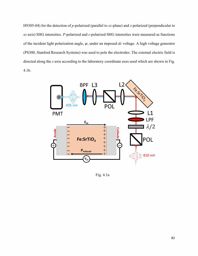
82
H9305-04) for the detection of p-polarized (parallel to xz-plane) and s-polarized (perpendicular to
xz-axis) SHG intensities. P-polarized and s-polarized SHG intensities were measured as functions
of the incident light polarization angle, 𝜑, under an imposed dc voltage. A high voltage generator
(PS300, Stanford Research Systems) was used to pole the electrodes. The external electric field is
directed along the z-axis according to the laboratory coordinate axes used which are shown in Fig.
4.1b.
Fig. 4.1a
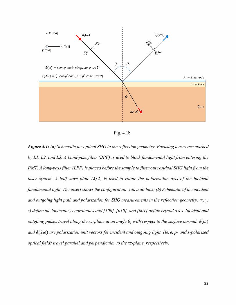
83
Fig. 4.1b
Figure 4.1: (a) Schematic for optical SHG in the reflection geometry. Focusing lenses are marked
by L1, L2, and L3. A band-pass filter (BPF) is used to block fundamental light from entering the
PMT. A long-pass filter (LPF) is placed before the sample to filter out residual SHG light from the
laser system. A half-wave plate (𝜆/2) is used to rotate the polarization axis of the incident
fundamental light. The insert shows the configuration with a dc-bias; (b) Schematic of the incident
and outgoing light path and polarization for SHG measurements in the reflection geometry. (x, y,
z) define the laboratory coordinates and [100], [010], and [001] define crystal axes. Incident and
outgoing pulses travel along the xz-plane at an angle 𝜃6 with respect to the surface normal. 𝑒(𝜔)
and 𝑒(2𝜔) are polarization unit vectors for incident and outgoing light. Here, p- and s-polarized
optical fields travel parallel and perpendicular to the xz-plane, respectively.

84
The coherence length for SHG radiation propagating through Fe:STO in the reflection (+) and
transmission (-) geometries is given by Eq. 3.10[82, 85]. As previously mentioned in chapter 3,
this length represents the maximum distance SHG light can travel through the crystal before its
intensity decreases due to destructive interference with itself. For incident light of wavelength 810
nm, the coherence length in the reflection geometry is about 40 nm. As a result, SHG intensities
reflected from the Pt-Fe:STO interface arise primarily from electric-dipole contributions in the
interfacial region, i.e. the Fe:STO surface[82].
The leading order contributions to the second-order polarization of the interfacial region can
be expressed as[37, 85, 105]:
𝑷b ∝ 𝜒(b)𝑬𝑬 +𝜒(c)𝑬𝑬𝑬â (4.1)
The first and second terms account for crystallographic and electrostatic field-induced dipole
contributions, respectively. At room temperature, pristine Fe:STO exhibits cubic (Pm3m)
symmetry in the bulk. Although the cubic bulk is largely centrosymmetric, inversion symmetry is
inherently broken at the surface due to atomic displacements that lead to tetragonal (4mm)
symmetry[106]. We can expand the i-th Cartesian coordinate of the second-order polarization in
Eq. 4.1 as follows:
𝑃6 2𝜔 = 𝜖$ 𝜒6µ�b (2𝜔;𝜔,𝜔)𝐸µ#$S 𝜔 𝐸�#$S 𝜔
µ�
+ 𝜖$ 𝜒6µ�#c (2𝜔;𝜔,𝜔, 0)𝐸µ#$S 𝜔 𝐸�#$S 𝜔 𝐸##$S 0
µ�#
(4.2)

85
The first term in the expression accounts for the electric-dipole contribution from the interfacial
region, e.g. Fe:STO surface polarity[56, 57]. The second term accounts for the electrostatic field-
induced dipole contribution which gives rise to the electric field-induced SHG (EFISHG) response
[107-110]. Here, 𝐸#$S 𝜔 = 𝐿(𝜔) ∙ 𝑬(𝜔), where 𝐿(𝜔) = 𝐿HH 𝚤𝚤 + 𝐿]] 𝚥𝚥 + 𝐿GG 𝑘𝑘 is a as discussed
in Section 3.3. The 𝐸##$S 0 term in Eq. 4.2 represents the l-th Cartesian coordinate of the dc-field
within the interfacial region. We take l = z for all calculations since the dc-field is applied along
the z-axis, parallel to the surface normal axis of the crystal. The non-vanishing components of the
second-order and third-order susceptibility tensors in Eq. 4.2 depend on the structural symmetry
of the probed region, which is tetragonal (4mm) symmetry [39]. The third-order EFISHG terms
can be reduced to an effective second-order term when taking l = z and integrating over the
interfacial region such that we obtain:
𝜒6µ�Gc (2𝜔;𝜔,𝜔, 0)𝐸G#$S 0 𝑑𝑧 𝐸µ#$S 𝜔 𝐸�#$S 𝜔
µ�
= 𝜒6µ�b (2𝜔;𝜔,𝜔)(𝐸G#$S)𝐸µ#$S 𝜔 𝐸�#$S 𝜔
µ�
(4.3)
The transformed second-order EFISHG susceptibility,𝜒6µ�b (2𝜔;𝜔,𝜔)(𝐸G#$S), has the same
symmetry properties as 𝜒6µ�b (2𝜔;𝜔,𝜔) for an imposed dc-field along the z-axis. For tetragonal
(4mm) symmetry, the non-vanishing second-order susceptibility components are 𝜒GGG, 𝜒HGH =
𝜒]G], 𝜒HHG = 𝜒]]G, and 𝜒GHH = 𝜒G]]. Using Eq. 4.2 and Eq. 4.3 we can explicitly solve for the
components of 𝑷(2𝜔):
86
𝑃H 2𝜔 = 2𝜖$ 2𝜒HHG(b) 𝐸H#$S 𝜔 𝐸G#$S 𝜔
+2𝜖$ 2𝜒HHGb (𝐸G#$S)𝐸H#$S 𝜔 𝐸G#$S(𝜔)
(4.4a)
𝑃] 2𝜔 = 2𝜖$ 2𝜒HHG(b) 𝐸]#$S 𝜔 𝐸G#$S 𝜔
+2𝜖$ 2𝜒HHGb (𝐸G#$S)𝐸]#$S 𝜔 𝐸G#$S(𝜔)
(4.4b)
𝑃G 2𝜔 = 2𝜖$ 𝜒GHHb 𝐸H#$S 𝜔 b + 𝜒GHH
b 𝐸]#$S 𝜔 b + 𝜒GGGb 𝐸G#$S 𝜔 b
+ 2𝜖$ 𝜒GHHb 𝐸G#$S 𝐸H#$S 𝜔 b + 𝜒HHG
b 𝐸G#$S 𝐸]#$S 𝜔 b
+ 𝜒GGGb 𝐸G#$S 𝐸G#$S 𝜔 b
(4.4c)
From the second-order nonlinear polarization, an effective second-order susceptibility for the
4mm interfacial region can be extracted using the following expression [39, 57, 98, 99, 111]:
𝜒[))(b) = 𝐿(2𝜔) ∙ 𝑒(2𝜔) ∙
𝑷(2𝜔)2𝜖$ 𝐸 b
(4.5)
Here, 𝐿(2𝜔) = 𝐿HHb𝚤𝚤 + 𝐿]]b𝚥𝚥 + 𝐿GGb𝑘𝑘 is a diagonal tensor consisting of Fresnel transformation
factors for double-frequency, or SHG, light propagating through the interfacial region and 𝑒(2𝜔)
is the polarization directional vector for the SHG electric fields reflected from the interface as
shown in Fig. 4.1b. The effective nonlinear susceptibility takes the following form:

87
𝜒[))(b) = −𝐿HHb𝑐𝑜𝑠𝜃𝑐𝑜𝑠𝜑Æ 2𝜒HHG
[))𝐿HH 𝐿GG 𝑠𝑖𝑛𝜃𝑐𝑜𝑠𝜃𝑐𝑜𝑠b𝜑 +𝐿]]b𝑠𝑖𝑛𝜑Æ 𝜒HHG
[))𝐿]] 𝐿GG 𝑠𝑖𝑛𝜃𝑠𝑖𝑛2𝜑 +𝐿GGb𝑠𝑖𝑛𝜃𝑐𝑜𝑠𝜑′ 𝜒GHH
[)) 𝐿HH b𝑐𝑜𝑠b𝜃𝑐𝑜𝑠b𝜑 + 𝜒GHH[)) 𝐿]]
b𝑠𝑖𝑛b𝜑 +
𝜒GGG[)) 𝐿GG b𝑠𝑖𝑛b𝜃𝑐𝑜𝑠b𝜑
(4.6)
Where
𝜒HHG[)) = 𝜒HHG + 𝛿𝜒HHG(𝐸G#$S)
𝜒GHH[)) = 𝜒GHH + 𝛿𝜒GHH(𝐸G#$S)
𝜒GGG[)) = 𝜒GGG + 𝛿𝜒GGG(𝐸G#$S)
The above three equations represent the effective second-order susceptibility components
expressed as functions of the local electric-field in the interfacial region. The terms 𝛿𝜒HHG(𝐸G#$S),
𝛿𝜒GHH(𝐸G#$S), and 𝛿𝜒GGG(𝐸G#$S) are field-induced susceptibility changes within the probed
interfacial region and describe electrostrictive distortions resulting from the applied dc electric
field. For a typical ABO3 perovskite structure, these perturbative terms have been previously
expressed as[112-114]:
𝛿𝜒GGG(𝐸G#$S) ∝ 𝛿A + 𝛿k(C) (4.7a)
𝛿𝜒GHH(𝐸G#$S) ∝ 𝛿A + 𝛿k(CC) (4.7b)
In Eq. 4.7, 𝛿A and 𝛿k are dc-field induced displacements for the B-site Fe:Ti cations and O-site
oxygen anions as discussed by Levine et al. [112, 113]. In this polarizable bond-charge model,
𝛿𝜒GGG(𝐸G#$S) is qualitatively interpreted as a stretching of the Fe:Ti-O bonds along the dc electric
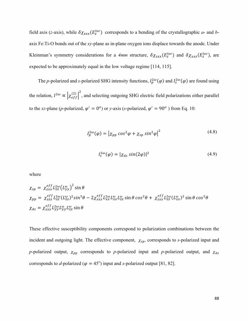
88
field axis (z-axis), while 𝛿𝜒GHH(𝐸G#$S) corresponds to a bending of the crystallographic a- and b-
axis Fe:Ti-O bonds out of the xy-plane as in-plane oxygen ions displace towards the anode. Under
Kleinman’s symmetry considerations for a 4mm structure, 𝛿𝜒GHH(𝐸G#$S) and 𝛿𝜒HHG 𝐸G#$S , are
expected to be approximately equal in the low voltage regime [114, 115].
The p-polarized and s-polarized SHG intensity functions, 𝐼<b 𝜑 and 𝐼%b 𝜑 are found using
the relation, 𝐼b ∝ 𝜒[))(b) b
, and selecting outgoing SHG electric field polarizations either parallel
to the xz-plane (p-polarized, 𝜑Æ = 0ä) or y-axis (s-polarized, 𝜑Æ = 90ä ) from Eq. 10:
𝐼<b 𝜑 = 𝜒<<𝑐𝑜𝑠b𝜑 + 𝜒%<𝑠𝑖𝑛b𝜑b (4.8)
𝐼%b 𝜑 = 𝜒"%𝑠𝑖𝑛 2𝜑 b (4.9)
where
𝜒%< = 𝜒GHH[))𝐿GGb 𝐿]]
b sin 𝜃
𝜒<< = 𝜒GGG[))𝐿GGb 𝐿GG b𝑠𝑖𝑛c𝜃 − 2𝜒HHG
[))𝐿HHb𝐿HH 𝐿GG sin 𝜃 𝑐𝑜𝑠b𝜃 +𝜒GHH[))𝐿GGb 𝐿HH b sin 𝜃 𝑐𝑜𝑠b𝜃
𝜒"% = 𝜒HHG[))𝐿]]b𝐿]] 𝐿GG sin 𝜃
These effective susceptibility components correspond to polarization combinations between the
incident and outgoing light. The effective component, 𝜒%<, corresponds to s-polarized input and
p-polarized output, 𝜒<< corresponds to p-polarized input and p-polarized output, and 𝜒"%
corresponds to d-polarized (𝜑 = 45o) input and s-polarized output [81, 82].
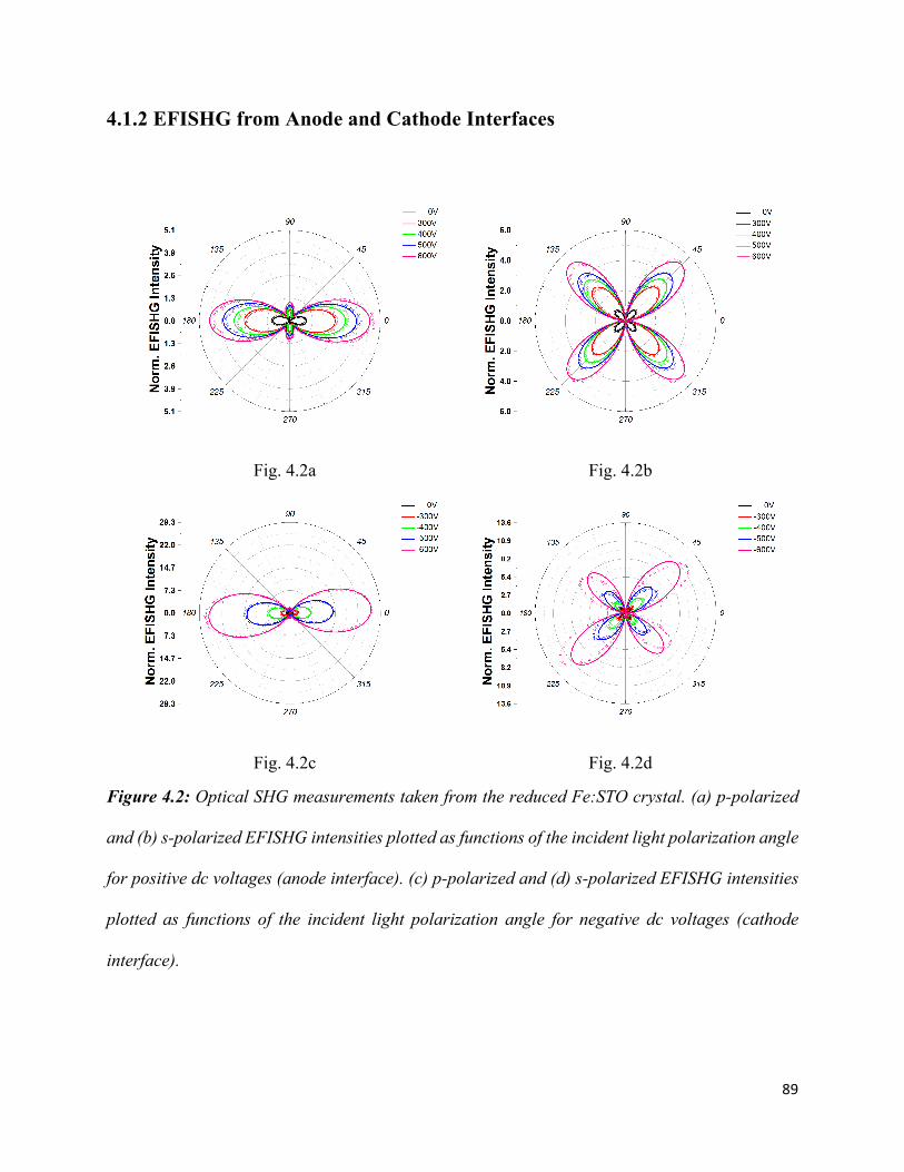
89
4.1.2 EFISHG from Anode and Cathode Interfaces
Fig. 4.2a Fig. 4.2b
Fig. 4.2c Fig. 4.2d
Figure 4.2: Optical SHG measurements taken from the reduced Fe:STO crystal. (a) p-polarized
and (b) s-polarized EFISHG intensities plotted as functions of the incident light polarization angle
for positive dc voltages (anode interface). (c) p-polarized and (d) s-polarized EFISHG intensities
plotted as functions of the incident light polarization angle for negative dc voltages (cathode
interface).
90
Fig. 4.2 shows p-polarized and s-polarized SHG intensities measured from the reduced
Fe:STO crystal under an imposed dc-bias. Solid lines show fits obtained using Eq. 4.8 and Eq. 4.9.
Magnitudes have been normalized in Fig. 2 with respect to the 0 V signals. The p-polarized and s-
polarized SHG intensities increase by factors of ~5.0 under forward dc-bias (0V to 600V). Under
reverse dc-bias (0V to -600V), p-polarized and s-polarized SHG intensities increase by factors of
~29.0 and ~11.5, respectively. Both out-of-plane and in-plane field-induced symmetry breaking at
the reduced Fe:STO interface are greater under reverse dc-bias. The fits for Fig. 4.2d are improved
by including a 𝜑-independent susceptibility term, i.e. 𝐼%b 𝜑 ~ 𝜒"%𝑠𝑖𝑛 2𝜑 + 𝜒$ b. The
apparent difference in magnitude between 𝐼%(45$) and 𝐼%(135$) for Fig. 4.2d spectra grows as the
imposed dc voltage increases, making fits worse. This can be explained by a field-induced
breaking of in-plane tetragonal (4mm) isotropy.
Fig. 4.3a Fig. 4.3b

91
Fig. 4.3c Fig. 4.3d
Figure 4.3: Optical SHG measurements taken from the oxidized Fe:STO crystal. (a) p-polarized
and (b) s-polarized EFISHG intensities plotted as functions of the incident light polarization angle
for positive dc voltages (anode interface). (c) p-polarized and (d) s-polarized EFISHG intensities
plotted as functions of the incident light polarization angle for negative dc voltages (cathode
interface).
In comparison, p-polarized and s-polarized SHG intensities were also measured from the
oxidized Fe:STO crystal under an imposed dc-bias, as shown in Fig. 4.3. Solid lines indicate fits
using Eq. 4.8 and Eq. 4.9. The p-polarized and s-polarized SHG intensities increase by factors of
~19.5 and ~14.5, respectively, under forward dc-bias (0V to 1200V). Under reverse dc-bias (0V
to -1800V), p-polarized and s-polarized SHG intensities increase by factors of ~2.5. This shows
both out-of-plane and in-plane field-induced symmetry breaking under forward dc-bias at the
oxidized Fe:STO interface.

92
Fig. 4.4a Fig. 4.4b
Fig. 4.4c
Fig. 4.4d
Figure 4.4: EFISHG intensities and susceptibilities as functions of the imposed voltage. EFISHG
intensities plotted as functions of the imposed dc voltage for the (a) reduced Fe:STO and (b)
oxidized Fe:STO single crystals. Effective susceptibilities plotted as functions of the imposed dc
voltage for the (c) reduced Fe:STO and (d) oxidized Fe:STO single crystals. Arrows point to
parabolic minima. EFISHG intensities above 1200V in Fig. 5b were predicted from fitting.
Fig. 4.4a and Fig. 4.4b show EFISHG intensities as functions of the imposed dc voltage for the
reduced and oxidized Fe:STO crystals. We extract the effective susceptibility components for
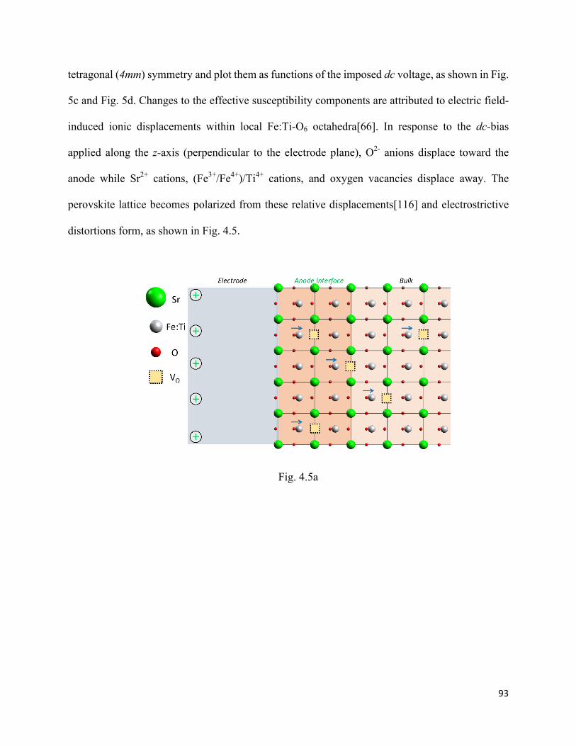
93
tetragonal (4mm) symmetry and plot them as functions of the imposed dc voltage, as shown in Fig.
5c and Fig. 5d. Changes to the effective susceptibility components are attributed to electric field-
induced ionic displacements within local Fe:Ti-O6 octahedra[66]. In response to the dc-bias
applied along the z-axis (perpendicular to the electrode plane), O2- anions displace toward the
anode while Sr2+ cations, (Fe3+/Fe4+)/Ti4+ cations, and oxygen vacancies displace away. The
perovskite lattice becomes polarized from these relative displacements[116] and electrostrictive
distortions form, as shown in Fig. 4.5.
Fig. 4.5a
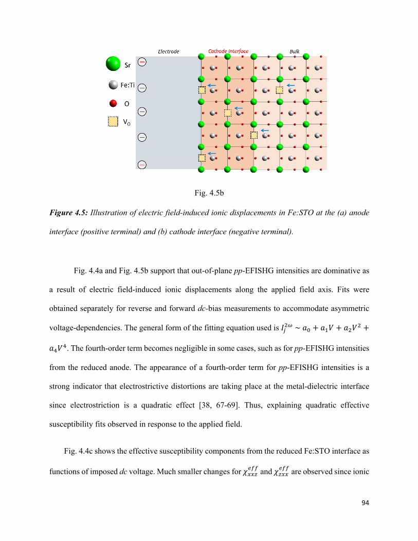
94
Fig. 4.5b
Figure 4.5: Illustration of electric field-induced ionic displacements in Fe:STO at the (a) anode
interface (positive terminal) and (b) cathode interface (negative terminal).
Fig. 4.4a and Fig. 4.5b support that out-of-plane pp-EFISHG intensities are dominative as
a result of electric field-induced ionic displacements along the applied field axis. Fits were
obtained separately for reverse and forward dc-bias measurements to accommodate asymmetric
voltage-dependencies. The general form of the fitting equation used is 𝐼µb~𝑎â + 𝑎a𝑉 + 𝑎b𝑉b +
𝑎p𝑉p. The fourth-order term becomes negligible in some cases, such as for pp-EFISHG intensities
from the reduced anode. The appearance of a fourth-order term for pp-EFISHG intensities is a
strong indicator that electrostrictive distortions are taking place at the metal-dielectric interface
since electrostriction is a quadratic effect [38, 67-69]. Thus, explaining quadratic effective
susceptibility fits observed in response to the applied field.
Fig. 4.4c shows the effective susceptibility components from the reduced Fe:STO interface as
functions of imposed dc voltage. Much smaller changes for 𝜒HHG[)) and 𝜒GHH
[)) are observed since ionic
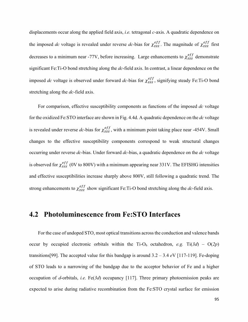
95
displacements occur along the applied field axis, i.e. tetragonal c-axis. A quadratic dependence on
the imposed dc voltage is revealed under reverse dc-bias for 𝜒GGG[)). The magnitude of 𝜒GGG
[)) first
decreases to a minimum near -77V, before increasing. Large enhancements to 𝜒GGG[)) demonstrate
significant Fe:Ti-O bond stretching along the dc-field axis. In contrast, a linear dependence on the
imposed dc voltage is observed under forward dc-bias for 𝜒GGG[)), signifying steady Fe:Ti-O bond
stretching along the dc-field axis.
For comparison, effective susceptibility components as functions of the imposed dc voltage
for the oxidized Fe:STO interface are shown in Fig. 4.4d. A quadratic dependence on the dc voltage
is revealed under reverse dc-bias for 𝜒GGG[)), with a minimum point taking place near -454V. Small
changes to the effective susceptibility components correspond to weak structural changes
occurring under reverse dc-bias. Under forward dc-bias, a quadratic dependence on the dc voltage
is observed for 𝜒GGG[)) (0V to 800V) with a minimum appearing near 331V. The EFISHG intensities
and effective susceptibilities increase sharply above 800V, still following a quadratic trend. The
strong enhancements to 𝜒GGG[)) show significant Fe:Ti-O bond stretching along the dc-field axis.
4.2 Photoluminescence from Fe:STO Interfaces
For the case of undoped STO, most optical transitions across the conduction and valence bands
occur by occupied electronic orbitals within the Ti-O6 octahedron, e.g. Ti(3d) – O(2p)
transitions[99]. The accepted value for this bandgap is around 3.2 – 3.4 eV [117-119]. Fe-doping
of STO leads to a narrowing of the bandgap due to the acceptor behavior of Fe and a higher
occupation of d-orbitals, i.e. Fe(3d) occupancy [117]. Three primary photoemission peaks are
expected to arise during radiative recombination from the Fe:STO crystal surface for emission
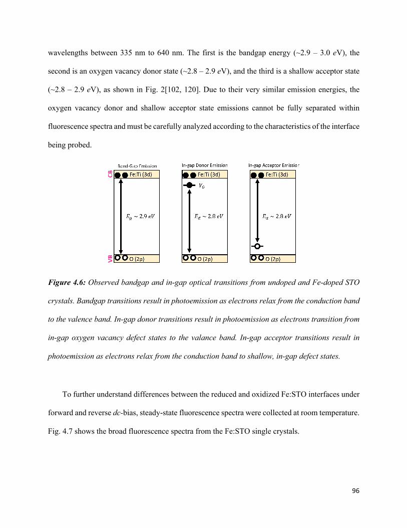
96
wavelengths between 335 nm to 640 nm. The first is the bandgap energy (~2.9 – 3.0 eV), the
second is an oxygen vacancy donor state (~2.8 – 2.9 eV), and the third is a shallow acceptor state
(~2.8 – 2.9 eV), as shown in Fig. 2[102, 120]. Due to their very similar emission energies, the
oxygen vacancy donor and shallow acceptor state emissions cannot be fully separated within
fluorescence spectra and must be carefully analyzed according to the characteristics of the interface
being probed.
Figure 4.6: Observed bandgap and in-gap optical transitions from undoped and Fe-doped STO
crystals. Bandgap transitions result in photoemission as electrons relax from the conduction band
to the valence band. In-gap donor transitions result in photoemission as electrons transition from
in-gap oxygen vacancy defect states to the valance band. In-gap acceptor transitions result in
photoemission as electrons relax from the conduction band to shallow, in-gap defect states.
To further understand differences between the reduced and oxidized Fe:STO interfaces under
forward and reverse dc-bias, steady-state fluorescence spectra were collected at room temperature.
Fig. 4.7 shows the broad fluorescence spectra from the Fe:STO single crystals.
97
Fig. 4.7a Fig. 4.7b
Figure 4.7: Fluorescence emission spectra for the (a) reduced and (b) oxidized Fe:STO interfaces.
Black curves show fits for the 0 V spectra while red and blue curves show fits for the cathode and
anode spectra, respectively. Photoemission energies for the two Gaussian peaks contributing to
each spectrum appear on the right side of each plot.
The black curves in Fig. 4.7a and Fig. 4.7b represent emission spectra for the reduced and oxidized
Fe:STO crystals without dc-field. Bandgap energies for the reduced and oxidized Fe:STO
interfaces were measured to be roughly 2.94eV at room temperature. Despite their similar emission
energies, oxygen vacancy donor states are expected to dominate in the reduced crystal while
shallow acceptor states are expected to dominate in the oxidized crystal.
For the reduced and oxidized Fe:STO emission spectra, both anode interfaces show
enhanced fluorescence intensities. This is attributed to two causes: (1) Increased radiative
recombination between the conduction and valence bands, i.e. Ti(3d) – O(2p) transitions, due to
the filling of O(2p) orbital sites as a result of local oxygen accumulation, and (2) Increased density
of excited holes which increases radiative recombination between conduction electrons and

98
shallow in-gap acceptor levels[101, 120]. In contrast, changes for the cathode emissions differ
significantly between the oxidized and reduced Fe:STO crystals. Fluorescence intensities decrease
for the reduced Fe:STO cathode, while intensities increase for the oxidized Fe:STO cathode. The
decrease in fluorescence for the reduced Fe:STO cathode can be attributed to the depopulation of
O(2p) sites due to the increased local oxygen vacancy concentration. The increase of oxygen
vacancies is accompanied by an increase in conduction electrons to conserve charge neutrality.
For the oxidized Fe:STO cathode, the increase in fluorescence is attributed to an increase in
emissions from oxygen vacancy donor levels.
Both EFISHG and photoluminescence measurements reveal that the reduced and oxidized
Fe:STO cathode interfaces behave differently due to their respective oxygen vacancy
concentrations. An excess of oxygen vacancies at the reduced cathode leads to significant
structural distortions as oxygen vacancy clustering leads to a depletion of O(2p) sites across the
valence band, driving the local lattice away from tetragonal (4mm) symmetry. In contrast,
moderate increases in the oxygen vacancy concentration at the oxidized cathode don’t cause any
structural symmetry changes due to higher oxygen concentrations. Instead, the fluorescence
intensity enhances simply due to increased oxygen vacancy donor states.
4.3 Schottky Junctions at Pt-Fe:STO Interfaces
In order to fully understand the EFISHG responses from the reduced and oxidized Fe:STO
interfaces, we look at the charged defect properties of each interface. Due to differing work
functions between the Pt electrode (ΦçE ∼ 5.65 – 6.35 eV)[121, 122] and Fe:STO (Φ�6 ∼ 4.3 eV,
Φ?[ ∼ 4.5 eV)[121, 122], these interfaces form Schottky junctions, as shown in Fig. 4.8[75, 123].
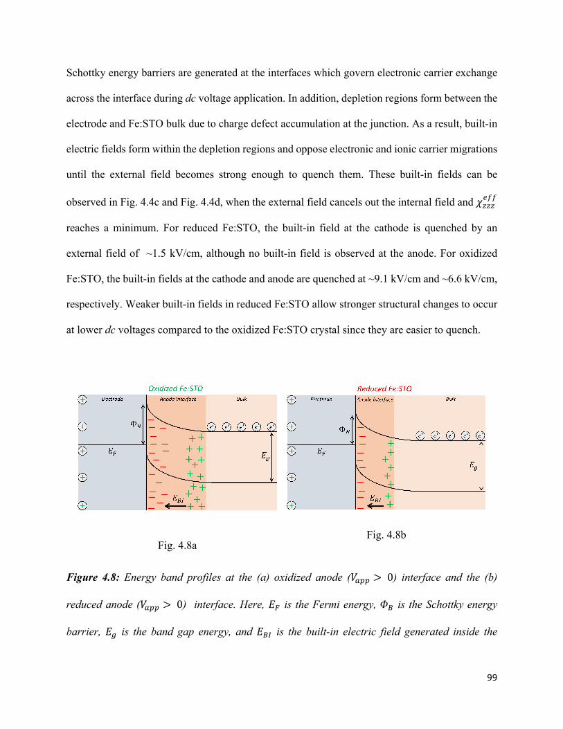
99
Schottky energy barriers are generated at the interfaces which govern electronic carrier exchange
across the interface during dc voltage application. In addition, depletion regions form between the
electrode and Fe:STO bulk due to charge defect accumulation at the junction. As a result, built-in
electric fields form within the depletion regions and oppose electronic and ionic carrier migrations
until the external field becomes strong enough to quench them. These built-in fields can be
observed in Fig. 4.4c and Fig. 4.4d, when the external field cancels out the internal field and 𝜒GGG[))
reaches a minimum. For reduced Fe:STO, the built-in field at the cathode is quenched by an
external field of ~1.5 kV/cm, although no built-in field is observed at the anode. For oxidized
Fe:STO, the built-in fields at the cathode and anode are quenched at ~9.1 kV/cm and ~6.6 kV/cm,
respectively. Weaker built-in fields in reduced Fe:STO allow stronger structural changes to occur
at lower dc voltages compared to the oxidized Fe:STO crystal since they are easier to quench.
Fig. 4.8a Fig. 4.8b
Figure 4.8: Energy band profiles at the (a) oxidized anode (𝑉;<< > 0) interface and the (b)
reduced anode (𝑉;<< > 0) interface. Here, 𝐸? is the Fermi energy, 𝛷A is the Schottky energy
barrier, 𝐸B is the band gap energy, and 𝐸AC is the built-in electric field generated inside the
100
interfacial region. The height of Schottky energy barrier is smaller in reduced Fe:STO compared
to oxidized Fe:STO, resulting in a thinner depletion region.
Under forward dc-bias, oxygen ions migrate towards the anode interface since the electrode
is positively poled. For reduced Fe:STO, no built-in electric field was observed at the anode
interface and may be explained by a very thin depletion region[123, 124]. Reduction annealing of
Fe:STO results in higher oxygen vacancy concentrations. Since oxygen vacancies behave as
donors, a decrease of the Schottky barrier height and depletion region width is expected in the
reduced crystal compared to the oxidized one[123, 125, 126]. This promotes charge migration
across the depletion region at lower dc voltages. In comparison, the built-in electric field at the
oxidized Fe:STO anode is stronger. Oxidation annealing of Fe:STO results in lower oxygen
vacancy and free carrier concentrations, thus increasing the Schottky barrier height and width of
the depletion region [123, 127]. Trapped charges within the depletion region result in the formation
of a much stronger built-in electric field at the oxidized Fe:STO interface compared to the reduced
Fe:STO interface. Below 800V, no significant electrostrictive distortions are observed since the
built-in field acts as a barrier, opposing oxygen vacancy migration. Above 800V, the external
electric field quenches the built-in field, resulting in a migration of trapped oxygen vacancies that
leads to strong, electrostrictive distortions[66, 72]. In particular, Fig. 5b and Fig. 5d exhibit strong
Schottky-like behavior, i.e. low straining under reverse dc-bias and strong straining under forward
dc-bias.
Under reverse dc-bias, oxygen vacancies migrate towards the cathode interface due to the
electrode being negatively poled. In contrast with the reduced Fe:STO anode, a weak built-in field
is seen at the cathode. This built-in field is easily quenched under low dc voltage which allows for
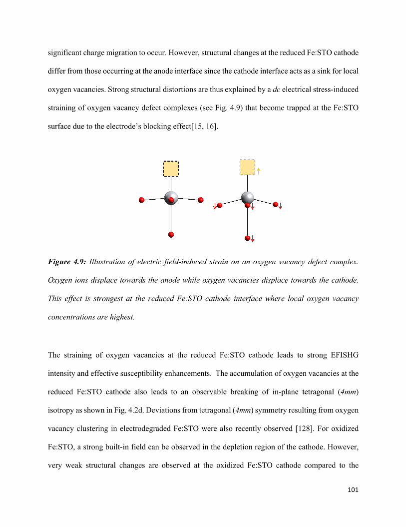
101
significant charge migration to occur. However, structural changes at the reduced Fe:STO cathode
differ from those occurring at the anode interface since the cathode interface acts as a sink for local
oxygen vacancies. Strong structural distortions are thus explained by a dc electrical stress-induced
straining of oxygen vacancy defect complexes (see Fig. 4.9) that become trapped at the Fe:STO
surface due to the electrode’s blocking effect[15, 16].
Figure 4.9: Illustration of electric field-induced strain on an oxygen vacancy defect complex.
Oxygen ions displace towards the anode while oxygen vacancies displace towards the cathode.
This effect is strongest at the reduced Fe:STO cathode interface where local oxygen vacancy
concentrations are highest.
The straining of oxygen vacancies at the reduced Fe:STO cathode leads to strong EFISHG
intensity and effective susceptibility enhancements. The accumulation of oxygen vacancies at the
reduced Fe:STO cathode also leads to an observable breaking of in-plane tetragonal (4mm)
isotropy as shown in Fig. 4.2d. Deviations from tetragonal (4mm) symmetry resulting from oxygen
vacancy clustering in electrodegraded Fe:STO were also recently observed [128]. For oxidized
Fe:STO, a strong built-in field can be observed in the depletion region of the cathode. However,
very weak structural changes are observed at the oxidized Fe:STO cathode compared to the
102
reduced one. Since oxidation leads to lower oxygen vacancy concentrations, vacancy accumulation
at this interface is considerably small and no straining of oxygen vacancies is observed.
4.4 Summary
In summary, electrostrictive distortions were detected at the reduced and oxidized Fe:STO
interfaces by measuring electric field-induced SHG intensity changes. The asymmetric voltage-
dependence of EFISHG intensities and effective susceptibilities is explained by the Schottky
behavior of the Pt-Fe:STO interfaces. Evidence shows that high oxygen vacancy concentrations
decrease Schottky barrier heights and depletion region widths, facilitating ionic and electronic
carrier transport near the interface. For reduced Fe:STO, structural changes at the anode are
explained by steady electrostrictive distortions of Fe:Ti-O6 octahedra as oxygen vacancies migrate
towards the cathode. Changes at the reduced Fe:STO cathode are explained by a dc electric field-
induced straining of oxygen vacancies trapped at the cathode surface due to the electrode’s
blocking effect. For oxidized Fe:STO, structural changes are due to strong electrostrictive
distortions as vacancies migrate to the cathode after the large built-in field in the depletion region
is quenched. In contrast to reduced Fe:STO, structural changes at the oxidized Fe:STO cathode are
very weak due to low oxygen vacancy concentrations.
Both EFISHG and photoluminescence measurements revealed different behaviors for the
cathodes of the reduced and oxidized Fe:STO single crystals. The clustering of oxygen vacancies
at the reduced cathode leads to a depopulation of O(2p) orbitals and a breaking of in-plane
tetragonal (4mm) isotropies. In contrast, no significant structural deviations from tetragonal (4mm)
symmetry are observed at the oxidized Fe:STO cathode due to its lower oxygen vacancy

103
concentration. Overall, the results show that optical SHG and photoluminescence are excellent
techniques for studying dc electric field-induced structural changes at electrode interfaces. We
show that oxygen vacancy concentration and diffusion play a critical role in the formation of
structural distortions at interfacial depletion regions.

104
Chapter 5: Formation of Structural Defects and Strain in Electrodegraded Fe-doped SrTiO3 Single Crystals due to Oxygen Vacancy Migration
This chapter presents the investigation of structural defect and strain formation resulting
from long-range oxygen vacancy migration in electrodegraded, reduced and oxidized Fe:STO
single crystals. Section 5.1 presents and discusses optical second harmonic generation (SHG)
measurements taken from the electrodegraded Fe:STO interfaces and bulk regions. Section 5.2
presents and discusses confocal Raman spectra collected from the electrodegraded Fe:STO bulk
regions. Section 5.3 provides a contextualized discussion of the oxygen vacancy migration-
induced structural changes presented in Sections 5.1 and 5.2. Section 5.4 summarizes the results
presented in this chapter.
5.1 Optical SHG from Electrodegraded Fe:STO Single Crystals
5.1.1 Experimental and Theoretical Description
Verneuil-grown, 10 x 10 x 0.5 mm3, (100) SrTiO3 single crystals doped with 0.01 wt% Fe
were cut into four, 5 x 5 x 0.5 mm3, pieces and epi-polished on both sides (MTI, Richmond, CA).
Crystals were annealed in a tube furnace at a temperature of 900 °C under a pO2 = 2x10⁻⁵ bar and
a pO2 = 0.2 bar, respectively. Afterwards, reduced crystals (B042, B057) were quenched in argon
(pO2 = 2x10⁻⁵ bar) whereas oxidized crystals (B045, B056) were quenched in air (pO2 = 0.2 bar) at
25 °C to freeze-in defect concentrations. As a result of these annealing and quenching procedures,

105
B042 and B057 have larger Fe3+ and 𝑉k∙∙ concentrations while B045 and B056 have larger Fe4+
concentrations, as shown in Table 3.1 [10, 51].
For B042 and B045, 10 nm planar, amorphous platinum electrodes were deposited on the
polished sample surfaces for longitudinal dc field application. These samples were placed in a
temperature bath of 210 oC under an applied dc voltage of 40V (Edc = 0.8 kV/cm for ~2.8 hours)
to induce oxygen ion and vacancy migrations towards the anode and cathode interfaces,
respectively[48]. For B056 and B057, 100 nm lateral, amorphous platinum electrodes were
deposited on the sample edges for transverse dc field application. These samples were placed in a
temperature bath of 210oC under an applied dc voltage of 100V (Edc = 0.2 kV/cm for ~27.8 hours)
to induce oxygen ion and vacancy migration. Fig. 5.1 shows the Fe:STO single crystals after the
electrodegradation process.
Figure 5.1: The top row of images shows the (a) schematic for dc voltage application across the
Fe:STO samples with planar electrodes and photographs of the electrodegraded (b) oxidized and
(c) reduced Fe:STO crystals with planar electrodes. Probed areas are labeled as the central, inner,
and outer regions (roughly 1 mm apart). The bottom row of images shows a (d) schematic for dc

106
voltage application across the Fe:STO samples with lateral electrodes and photographs of the
electrodegraded (e) oxidized and (f) reduced Fe:STO crystals with lateral electrodes. The anodic,
mixed, and cathodic regions are labeled under each sample. The red dashed lines in (e) and (f)
mark probed paths between electrodes.
Fig. 5.1a shows the setup for dc voltage application on Fe:STO crystals with planar electrodes
deposited on their 5 x 5 mm2 faces. Fig. 5.1b and Fig. 5.1c show B042 and B045 after the
electrodegradation process, i.e. after the onset of voltage-induced resistance degradation and
oxygen vacancy demixing. Inhomogeneous electrocoloration is clearly observable in the
B042/B045 crystals where darker regions absorb more visible light due to higher Fe4+ and oxygen
concentrations[20, 48]. Three regions of the electrodegraded interfaces in Fig. 5.1b and Fig. 5.1c
were probed, namely, the central, inner, and outer regions. These regions are named by their
relative distances from the center of the square interfacial plane. A distance of approximately 1
mm lies between the central and inner regions and the inner and outer regions. For comparison,
Fig. 1d shows the setup for dc voltage application on Fe:STO crystals with lateral electrodes grown
on their 5 x 0.5 mm2 sides. Fig. 5.1e and Fig. 5.1f show B056 and B057 after the electrodegradation
process. A more homogenized electrocoloration is observable across the B056/B057 crystals as
well as the formation of an electrocoloration boundary, or color front, between the anodic and
cathodic bulk regions. As shown in Fig. 3.3, an increase in current density by roughly two orders
of magnitude is observed in all crystals as a result of resistance degradation[4, 7].
For samples B042 and B045, optical SHG measurements were taken in the reflection
geometry in order to probe the nonlinear response of the degraded electrode interfaces. For samples
B056 and B057, optical SHG measurements were collected in the transmission geometry in order
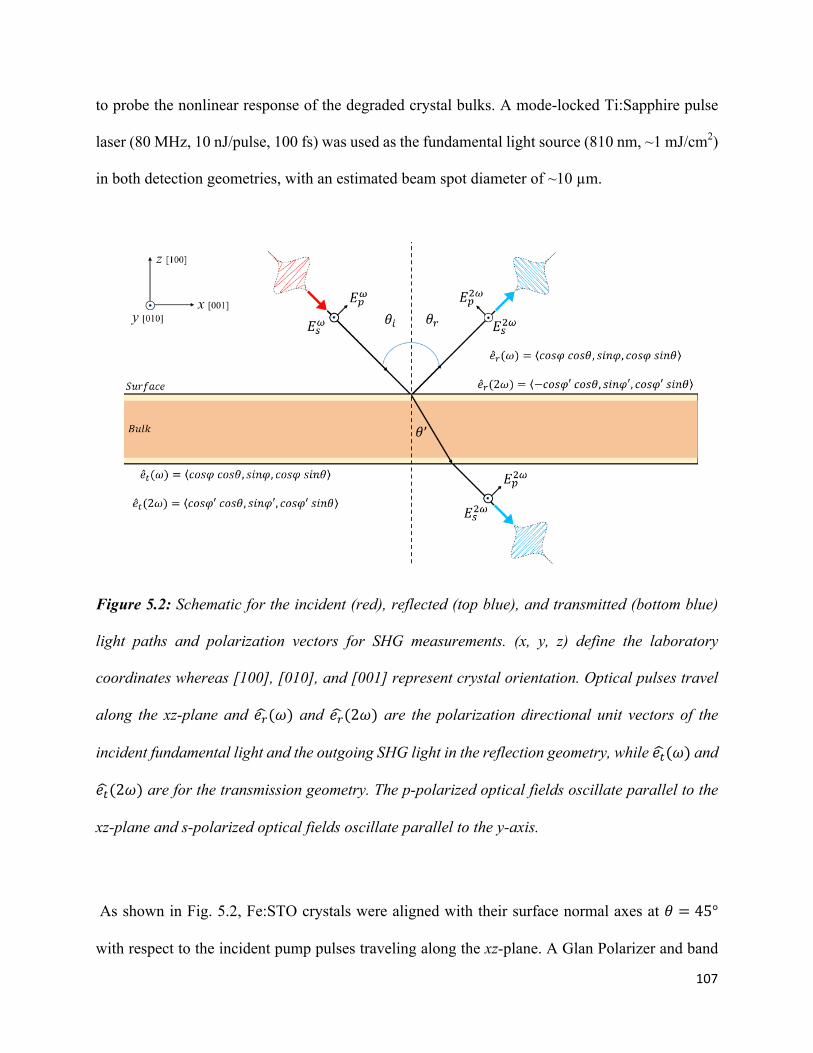
107
to probe the nonlinear response of the degraded crystal bulks. A mode-locked Ti:Sapphire pulse
laser (80 MHz, 10 nJ/pulse, 100 fs) was used as the fundamental light source (810 nm, ~1 mJ/cm2)
in both detection geometries, with an estimated beam spot diameter of ~10 µm.
Figure 5.2: Schematic for the incident (red), reflected (top blue), and transmitted (bottom blue)
light paths and polarization vectors for SHG measurements. (x, y, z) define the laboratory
coordinates whereas [100], [010], and [001] represent crystal orientation. Optical pulses travel
along the xz-plane and 𝑒D(𝜔) and 𝑒D(2𝜔) are the polarization directional unit vectors of the
incident fundamental light and the outgoing SHG light in the reflection geometry, while 𝑒E(𝜔) and
𝑒E(2𝜔) are for the transmission geometry. The p-polarized optical fields oscillate parallel to the
xz-plane and s-polarized optical fields oscillate parallel to the y-axis.
As shown in Fig. 5.2, Fe:STO crystals were aligned with their surface normal axes at 𝜃 = 45°
with respect to the incident pump pulses traveling along the xz-plane. A Glan Polarizer and band

108
pass filter (Thorlabs, FB400-40) were placed in front of a photomultiplier tube module
(Hamamatsu, H9305-04) connected to a lock-in amplifier for collecting p-polarized or s-polarized
SHG intensities as functions of the incident light polarization angle. The incident polarization
angle was rotated using a half-wavelength plate. For B042/B045, reflected SHG signals were
collected from three spots across the outer, inner, and central regions[128, 129]. For B056/B057,
transmitted SHG signals were measured across a ~4.5 mm path between the platinum electrodes,
covering the anodic, mixed, and cathodic bulk regions[130]. All SHG signals were detected at
room temperature, after completion of the electrodegradation process.
The SHG intensities,𝐼<t$êEb 𝜑 and 𝐼%t$êEb 𝜑 , can be expressed as functions of the
polarization angle 𝜑 of the incident pump pulses. Following the relation that 𝐼b ∝ 𝜒[))(b) b
and
selecting for outgoing SHG electric field polarizations parallel to the y-axis (s-polarized, 𝜑 = 90°)
or xz-plane (p-polarized, 𝜑 = 0°), the p-polarized and s-polarized SHG intensities are as follows
[97, 98, 110]:
𝐼<t$êEb 𝜑 = 𝜒<<𝑐𝑜𝑠b𝜑 + 𝜒%<𝑠𝑖𝑛b𝜑b (5.1)
𝐼%t$êEb 𝜑 = 𝜒"%𝑠𝑖𝑛 2𝜑 b (5.2)
where,
𝜒%< = 𝜒GHH𝐿GGb 𝐿]]b sin 𝜃
𝜒<< = 𝜒GGG𝐿GGb 𝐿GG b𝑠𝑖𝑛c𝜃 ∓ 2𝜒HHG𝐿HHb𝐿HH 𝐿GG sin 𝜃 𝑐𝑜𝑠b𝜃 +𝜒GHH𝐿GGb 𝐿HH b sin 𝜃 𝑐𝑜𝑠b𝜃
𝜒"% = 𝜒HHG𝐿]]b𝐿]] 𝐿GG sin 𝜃.
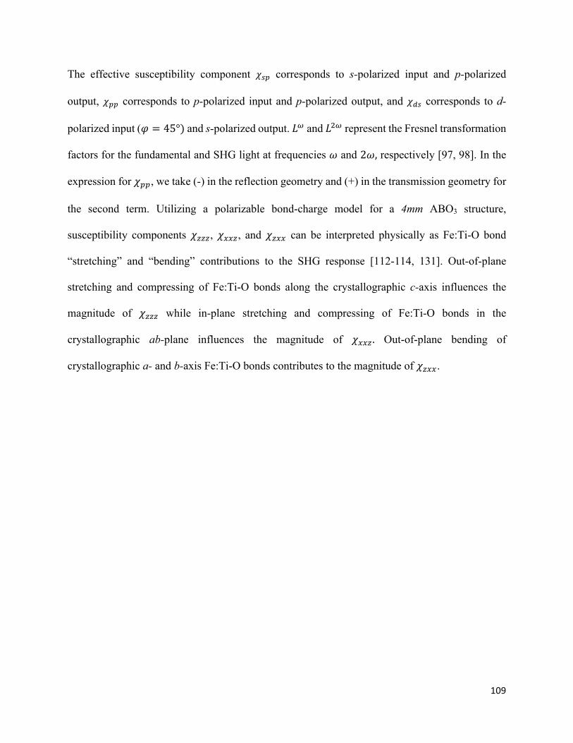
109
The effective susceptibility component 𝜒%< corresponds to s-polarized input and p-polarized
output, 𝜒<< corresponds to p-polarized input and p-polarized output, and 𝜒"% corresponds to d-
polarized input (𝜑 = 45°) and s-polarized output. 𝐿 and 𝐿b represent the Fresnel transformation
factors for the fundamental and SHG light at frequencies 𝜔 and 2𝜔, respectively [97, 98]. In the
expression for 𝜒<<, we take (-) in the reflection geometry and (+) in the transmission geometry for
the second term. Utilizing a polarizable bond-charge model for a 4mm ABO3 structure,
susceptibility components 𝜒GGG, 𝜒HHG, and 𝜒GHH can be interpreted physically as Fe:Ti-O bond
“stretching” and “bending” contributions to the SHG response [112-114, 131]. Out-of-plane
stretching and compressing of Fe:Ti-O bonds along the crystallographic c-axis influences the
magnitude of 𝜒GGG while in-plane stretching and compressing of Fe:Ti-O bonds in the
crystallographic ab-plane influences the magnitude of 𝜒HHG. Out-of-plane bending of
crystallographic a- and b-axis Fe:Ti-O bonds contributes to the magnitude of 𝜒GHH.
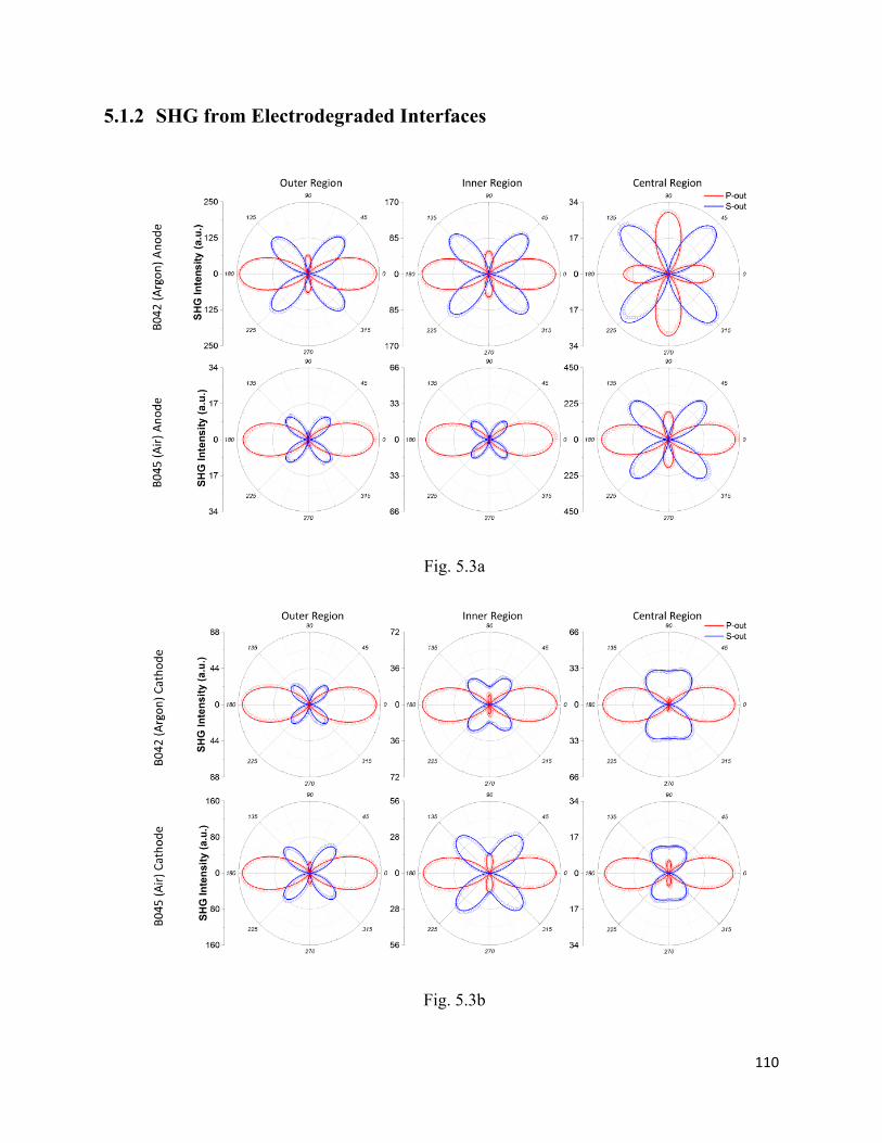
110
5.1.2 SHG from Electrodegraded Interfaces
Fig. 5.3a
Fig. 5.3b
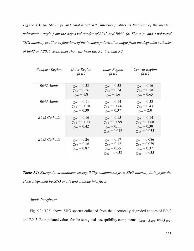
111
Figure 5.3: (a) Shows p- and s-polarized SHG intensity profiles as functions of the incident
polarization angle from the degraded anodes of B042 and B045. (b) Shows p- and s-polarized
SHG intensity profiles as functions of the incident polarization angle from the degraded cathodes
of B042 and B045. Solid lines show fits from Eq. 5.1, 5.2, and 5.3.
Sample / Region Outer Region (a.u.)
Inner Region (a.u.)
Central Region (a.u.)
B042 Anode χxxz = 0.38 χzxx = 0.26 χzzz = 1.8
χxxz = 0.33 χzxx = 0.24 χzzz = 1.6
χxxz = 0.16 χzxx = 0.18 χzzz = 0.65
B045 Anode χxxz = 0.11 χzxx = 0.058 χzzz = 0.39
χxxz = 0.14 χzxx = 0.066 χzzz = 0.37
χxxz = 0.53 χzxx = 0.43 χzzz = 2.0
B042 Cathode χxxz = 0.16 χzxx = 0.073 χzzz = 0.42
χxxz = 0.15 χzxx = 0.099 χzzz = 0.11 χyyy = 0.042
χxxz = 0.14 χzxx = 0.068 χzzz = 0.30 χyyy = 0.055
B045 Cathode χxxz = 0.26 χzxx = 0.16 χzzz = 0.87
χxxz = 0.17 χzxx = 0.12 χzzz = 0.55 χyyy = 0.038
χxxz = 0.086 χzxx = 0.079 χzzz = 0.37 χyyy = 0.035
Table 5.1: Extrapolated nonlinear susceptibility components from SHG intensity fittings for the
electrodegraded Fe:STO anode and cathode interfaces.
Anode Interfaces:
Fig. 5.3a[128] shows SHG spectra collected from the electrically degraded anodes of B042
and B045. Extrapolated values for the tetragonal susceptibility components, 𝜒GGG, 𝜒HHG, and 𝜒GHH,
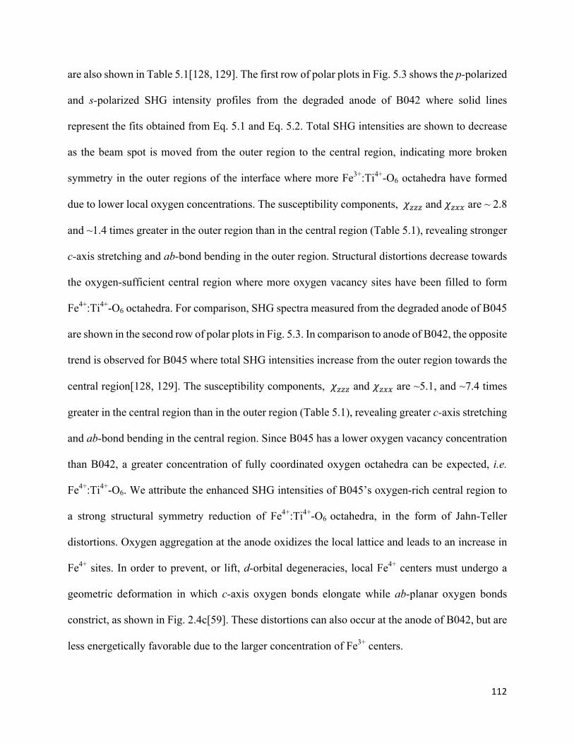
112
are also shown in Table 5.1[128, 129]. The first row of polar plots in Fig. 5.3 shows the p-polarized
and s-polarized SHG intensity profiles from the degraded anode of B042 where solid lines
represent the fits obtained from Eq. 5.1 and Eq. 5.2. Total SHG intensities are shown to decrease
as the beam spot is moved from the outer region to the central region, indicating more broken
symmetry in the outer regions of the interface where more Fe3+:Ti4+-O6 octahedra have formed
due to lower local oxygen concentrations. The susceptibility components, 𝜒GGG and 𝜒GHH are ~ 2.8
and ~1.4 times greater in the outer region than in the central region (Table 5.1), revealing stronger
c-axis stretching and ab-bond bending in the outer region. Structural distortions decrease towards
the oxygen-sufficient central region where more oxygen vacancy sites have been filled to form
Fe4+:Ti4+-O6 octahedra. For comparison, SHG spectra measured from the degraded anode of B045
are shown in the second row of polar plots in Fig. 5.3. In comparison to anode of B042, the opposite
trend is observed for B045 where total SHG intensities increase from the outer region towards the
central region[128, 129]. The susceptibility components, 𝜒GGG and 𝜒GHH are ~5.1, and ~7.4 times
greater in the central region than in the outer region (Table 5.1), revealing greater c-axis stretching
and ab-bond bending in the central region. Since B045 has a lower oxygen vacancy concentration
than B042, a greater concentration of fully coordinated oxygen octahedra can be expected, i.e.
Fe4+:Ti4+-O6. We attribute the enhanced SHG intensities of B045’s oxygen-rich central region to
a strong structural symmetry reduction of Fe4+:Ti4+-O6 octahedra, in the form of Jahn-Teller
distortions. Oxygen aggregation at the anode oxidizes the local lattice and leads to an increase in
Fe4+ sites. In order to prevent, or lift, d-orbital degeneracies, local Fe4+ centers must undergo a
geometric deformation in which c-axis oxygen bonds elongate while ab-planar oxygen bonds
constrict, as shown in Fig. 2.4c[59]. These distortions can also occur at the anode of B042, but are
less energetically favorable due to the larger concentration of Fe3+ centers.
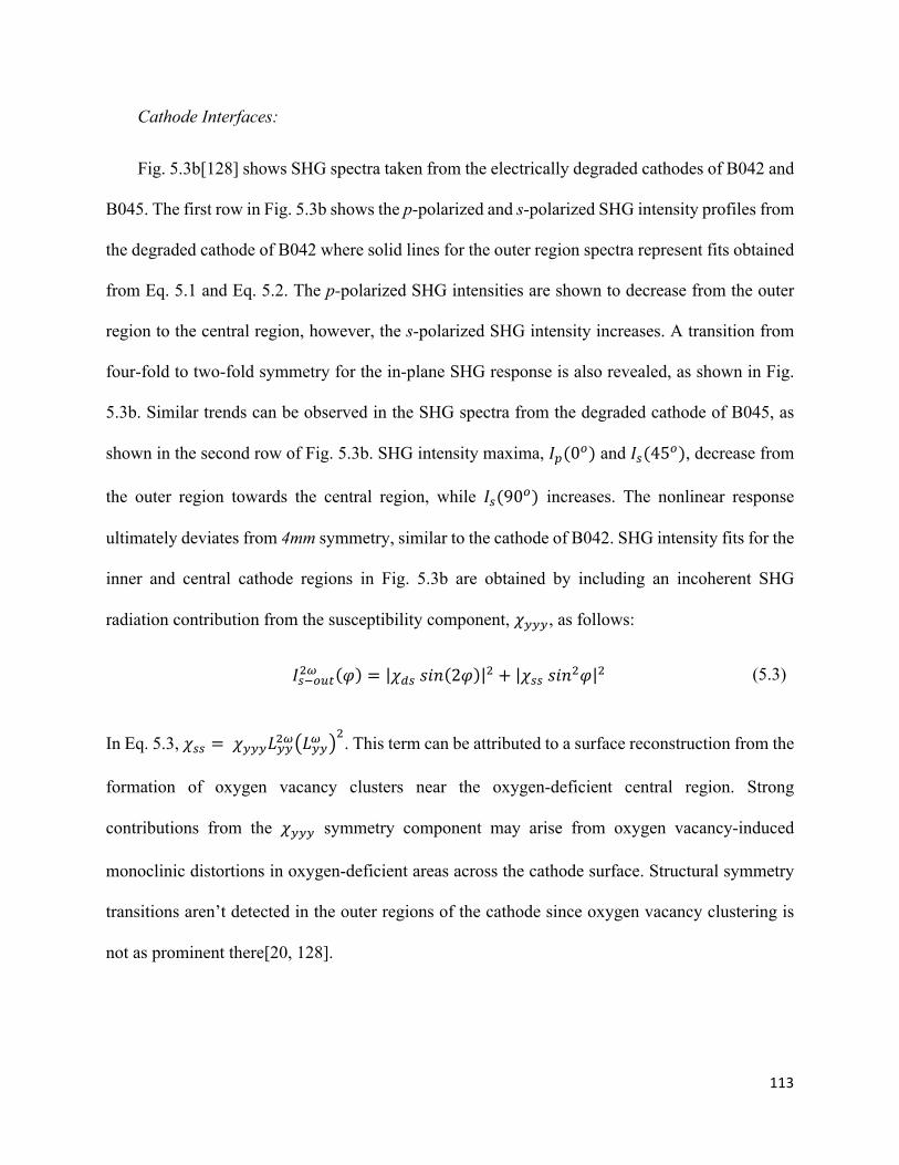
113
Cathode Interfaces:
Fig. 5.3b[128] shows SHG spectra taken from the electrically degraded cathodes of B042 and
B045. The first row in Fig. 5.3b shows the p-polarized and s-polarized SHG intensity profiles from
the degraded cathode of B042 where solid lines for the outer region spectra represent fits obtained
from Eq. 5.1 and Eq. 5.2. The p-polarized SHG intensities are shown to decrease from the outer
region to the central region, however, the s-polarized SHG intensity increases. A transition from
four-fold to two-fold symmetry for the in-plane SHG response is also revealed, as shown in Fig.
5.3b. Similar trends can be observed in the SHG spectra from the degraded cathode of B045, as
shown in the second row of Fig. 5.3b. SHG intensity maxima, 𝐼<(0$) and 𝐼%(45$), decrease from
the outer region towards the central region, while 𝐼%(90$) increases. The nonlinear response
ultimately deviates from 4mm symmetry, similar to the cathode of B042. SHG intensity fits for the
inner and central cathode regions in Fig. 5.3b are obtained by including an incoherent SHG
radiation contribution from the susceptibility component, 𝜒]]], as follows:
𝐼%t$êEb 𝜑 = 𝜒"%𝑠𝑖𝑛 2𝜑 b + 𝜒%%𝑠𝑖𝑛b𝜑 b (5.3)
In Eq. 5.3, 𝜒%% = 𝜒]]]𝐿]]b 𝐿]]b. This term can be attributed to a surface reconstruction from the
formation of oxygen vacancy clusters near the oxygen-deficient central region. Strong
contributions from the 𝜒]]] symmetry component may arise from oxygen vacancy-induced
monoclinic distortions in oxygen-deficient areas across the cathode surface. Structural symmetry
transitions aren’t detected in the outer regions of the cathode since oxygen vacancy clustering is
not as prominent there[20, 128].
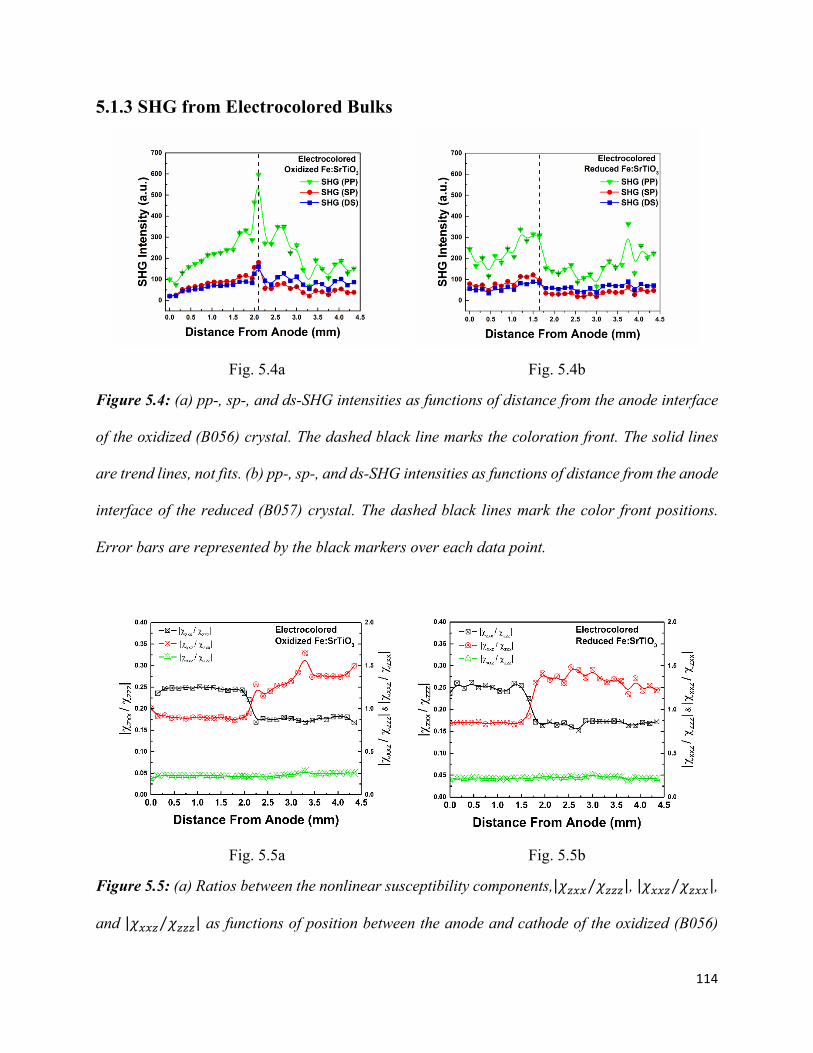
114
5.1.3 SHG from Electrocolored Bulks
Fig. 5.4a Fig. 5.4b
Figure 5.4: (a) pp-, sp-, and ds-SHG intensities as functions of distance from the anode interface
of the oxidized (B056) crystal. The dashed black line marks the coloration front. The solid lines
are trend lines, not fits. (b) pp-, sp-, and ds-SHG intensities as functions of distance from the anode
interface of the reduced (B057) crystal. The dashed black lines mark the color front positions.
Error bars are represented by the black markers over each data point.
Fig. 5.5a Fig. 5.5b
Figure 5.5: (a) Ratios between the nonlinear susceptibility components, 𝜒GHH 𝜒GGG , 𝜒HHG 𝜒GHH ,
and 𝜒HHG 𝜒GGG as functions of position between the anode and cathode of the oxidized (B056)
115
crystal. The solid lines are trend lines, not fits. (b) Ratios between the nonlinear susceptibility
components, 𝜒GHH 𝜒GGG , 𝜒HHG 𝜒GHH , and 𝜒HHG 𝜒GGG as functions of position between the anode
and cathode of the reduced (B057) crystal.
To further understand structural changes resulting from voltage-induced oxygen vacancy
migration in Fe:STO, optical SHG was also collected from electrocolored bulk phases of the B056
and B057 Fe:STO single crystals[130], as shown in Fig. 5.4. Fig. 5.4a shows the pp-, sp-, and ds-
SHG intensities plotted as functions of distance from the anode interface for B056, where the
vertical dashed line marks the coloration front position. In the anodic region, all three SHG
intensities increase gradually as the detection site moves towards the mixed region. The pp-SHG
intensity is larger than both sp- and ds-SHG intensities, with sp-SHG being greater than ds-SHG
in the anodic region. In the mixed region, the highest SHG intensities are observed with maxima
positioned on the coloration front. Past the coloration front, the SHG intensities decrease into the
cathodic region. For the cathodic region, ds-SHG increases over sp-SHG, opposite of what is
observed for the anodic region. The spatial distribution of SHG intensity provides a good estimate
for the structural strain distribution across the electrocolored crystal. Strain increases from the
anode towards the mixed region, and then decreases towards the cathode. The coloration front in
the mixed region marks an electrochemical interface between the anodic (p-type, dark brown) and
cathodic (n-type, light brown) bulk regions of the crystal. At this coloration front, a strain field has
formed due to dipole moments aligned between Fe4+:Ti4+-O6 and Fe3+:Ti4+-O6 octahedra packed
along the front [85, 97].
Fig. 5.4b shows the pp-, sp-, and ds-SHG intensities plotted as functions of distance from the
anode interface for B056, where the vertical dashed line marks the coloration front position. In the

116
anodic region, SHG intensities decrease slightly into the anodic region before increasing towards
the mixed region. Similar to the SHG measurements from B056, the pp-SHG intensity is larger
than both sp- and ds-SHG intensities, with sp-SHG being greater than ds-SHG in the anodic region.
In the mixed region, strong SHG intensities are observed on the coloration front before decreasing
into the cathodic region. Again, we observe that ds-SHG increases over sp-SHG in the cathodic
region. Relating SHG intensity to the degree of structural strain across the electrocolored crystal,
strain is seen to be largest near the anode interface, coloration front, and cathode interface.
In order to understand the structural changes across the oxidized (B056) and reduced (B057)
crystals, ratios between the nonlinear susceptibility components, 𝜒GHH 𝜒GGG , 𝜒HHG 𝜒GHH , and
𝜒HHG 𝜒GGG were calculated from the SHG intensity measurements as shown in Fig. 6a and Fig.
6b. For the perovskite (ABO3) structure, the susceptibility components can be interpreted as Fe:Ti-
O bond “stretching” and “bending” contributions to the SHG response which occur in the Fe:Ti-
O6 octahedra [112-114]. Out-of-plane and in-plane Fe:Ti-O bond stretching contributions are
linked to 𝜒GGG and 𝜒HHG, respectively, while Fe:Ti-O bond bending contributions are linked to 𝜒GHH.
Ratios between these components allow us to observe the relative strength of bond stretching and
bending effects in each region. From 𝜒GHH 𝜒GGG and 𝜒HHG 𝜒GHH we identify that the anodic bulk
has larger Fe:Ti-O bond bending contributions around Fe4+ defect centers, while the cathodic bulk
shows larger Fe:Ti-O bond stretching around Fe3+ defect centers [48, 59]. Greater bond bending
in the anodic region is explained by the presence of Jahn-Teller type distortions around Fe4+ defect
centers. This attribution is supported by previous structural and optical spectroscopic studies which
have shown strong evidence of Jahn-Teller distortions as well as modified Fe:Ti-O bond lengths
and B-O-B (Fe:Ti cations at the B-sites, oxygen anions at the O-sites) bond bending angles around
Fe4+ centers in Fe-doped SrTiO3 perovskites.[59] Greater bond stretching in the cathodic region

117
can be attributed to the presence of tetragonal Fe3+ defect centers such as (Fe3+- 𝑉k∙∙) defects [4].
This attribution is supported by past EXAFS and XANES measurements performed on
electrocolored Fe:STO. Longer Fe-O bond lengths were revealed in cathodic regions (compared
to anodic regions) [48]. The Fe:Ti-O bond stretching in the cathodic bulks is also relevant to the
formation of tetragonal (Fe3+ -𝑉k∙∙) defects.
The mixed region in B056 appears between 1.95 mm – 2.25 mm, as seen in Fig. 5.5a, with an
effective thickness of ~ 0.3 mm. For B057, the mixed region is marked between 1.5 mm – 1.95
mm with an effective thickness of ~ 0.45 mm, as shown in Fig. 5.5b. The thinner anodic region of
B057 compared to B056 can be explained by the oxygen vacancy concentration differences
between the two samples (Table 1). In both crystals, the susceptibility ratios, 𝜒GHH 𝜒GGG and
𝜒HHG 𝜒GHH , undergo a clear transition across the coloration front, exhibiting more bond bending
and stretching on the anodic and cathodic sides of samples, respectively. As a result, the coloration
front is not only an electrochemical interface between two dominating Fe oxidation states, but also
a structural interface between two different kinds of crystal distortion. Structural strain is the
highest in this region, with non-centrosymmetric Fe4+ and Fe3+ defect centers packed along the
anodic and cathodic sides of the coloration front, respectively. Strong strain fields have formed
due to dipole moments aligned between Fe4+:Ti4+-O6 and Fe3+:Ti4+-O6 octahedra packed along the
color fronts [85, 97]. Even though both crystals show evidence of existing strain fields at their
color fronts, larger SHG intensities in B056 show greater strain compared to B057. This suggests
that oxygen vacancy migration plays an important role in strain relaxation near the color fronts.
We expect the oxidized crystal to have fewer oxygen vacancy diffusion pathways, leading to a less
efficient demixing process during degradation [20]. As a result, more charge trap centers formed
near the color front of the oxidized crystal compared to the reduced sample. Lastly, the 𝜒HHG 𝜒GGG
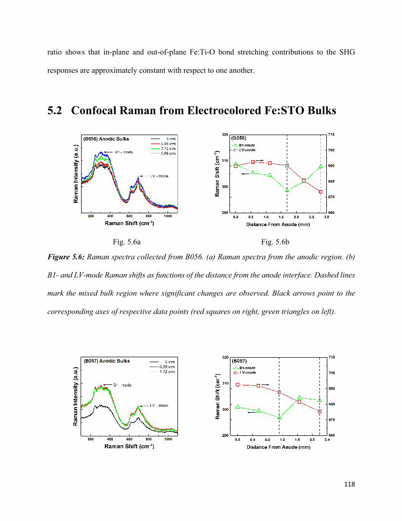
118
ratio shows that in-plane and out-of-plane Fe:Ti-O bond stretching contributions to the SHG
responses are approximately constant with respect to one another.
5.2 Confocal Raman from Electrocolored Fe:STO Bulks
Fig. 5.6a Fig. 5.6b
Figure 5.6: Raman spectra collected from B056. (a) Raman spectra from the anodic region. (b)
B1- and LV-mode Raman shifts as functions of the distance from the anode interface. Dashed lines
mark the mixed bulk region where significant changes are observed. Black arrows point to the
corresponding axes of respective data points (red squares on right, green triangles on left).
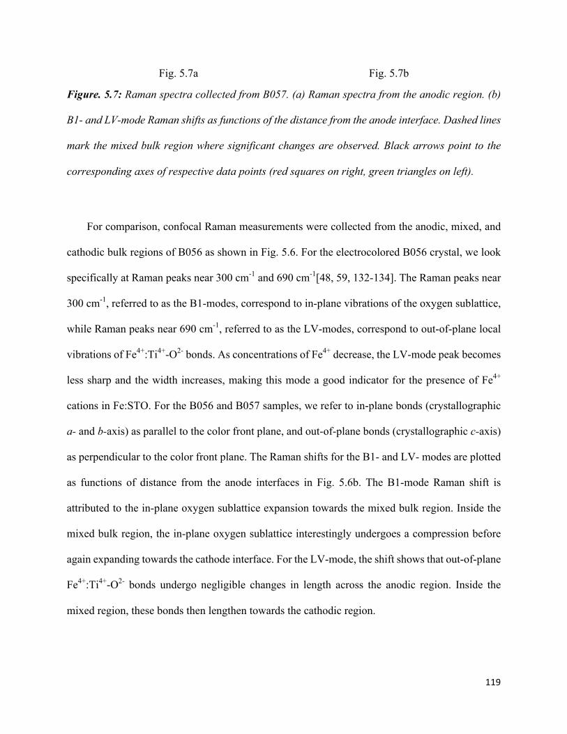
119
Fig. 5.7a Fig. 5.7b
Figure. 5.7: Raman spectra collected from B057. (a) Raman spectra from the anodic region. (b)
B1- and LV-mode Raman shifts as functions of the distance from the anode interface. Dashed lines
mark the mixed bulk region where significant changes are observed. Black arrows point to the
corresponding axes of respective data points (red squares on right, green triangles on left).
For comparison, confocal Raman measurements were collected from the anodic, mixed, and
cathodic bulk regions of B056 as shown in Fig. 5.6. For the electrocolored B056 crystal, we look
specifically at Raman peaks near 300 cm-1 and 690 cm-1[48, 59, 132-134]. The Raman peaks near
300 cm-1, referred to as the B1-modes, correspond to in-plane vibrations of the oxygen sublattice,
while Raman peaks near 690 cm-1, referred to as the LV-modes, correspond to out-of-plane local
vibrations of Fe4+:Ti4+-O2- bonds. As concentrations of Fe4+ decrease, the LV-mode peak becomes
less sharp and the width increases, making this mode a good indicator for the presence of Fe4+
cations in Fe:STO. For the B056 and B057 samples, we refer to in-plane bonds (crystallographic
a- and b-axis) as parallel to the color front plane, and out-of-plane bonds (crystallographic c-axis)
as perpendicular to the color front plane. The Raman shifts for the B1- and LV- modes are plotted
as functions of distance from the anode interfaces in Fig. 5.6b. The B1-mode Raman shift is
attributed to the in-plane oxygen sublattice expansion towards the mixed bulk region. Inside the
mixed bulk region, the in-plane oxygen sublattice interestingly undergoes a compression before
again expanding towards the cathode interface. For the LV-mode, the shift shows that out-of-plane
Fe4+:Ti4+-O2- bonds undergo negligible changes in length across the anodic region. Inside the
mixed region, these bonds then lengthen towards the cathodic region.

120
Raman measurements collected from the anodic, mixed, and cathodic bulk phases of B057
are shown in Fig. 5.7. Fig. 5.7b shows the Raman shifts for the B1- and LV-mode plotted as
functions of distance from the anode interface for B057. For the B1-mode, we show that the in-
plane oxygen sublattice expands towards the mixed bulk region, similar to B056. Near the mixed
bulk region, the in-plane oxygen sublattice compresses before expanding slightly within the
cathodic region, then compresses again near the cathode interface. For the LV-mode, out-of-plane
Fe4+:Ti4+-O2- bonds undergo a lengthening from the anode interface into the cathodic region.
The Raman shift changes to the B1- and LV-modes between the anode and cathode show
significant structural changes due to oxygen vacancy electromigration, consistent with SHG
results[130]. For the anodic bulk regions of B056 and B057, as shown in Fig. 5.6b and Fig. 5.6b,
the strong presence of Fe4+, shorter in-plane oxygen bonds, and longer out-of-plane oxygen bonds
support the formation of Jahn-Teller distortions. Increases for B1-mode shifts and decreases for
LV-mode shifts are identified across both mixed regions are observed. This result confirms the
compression of in-plane oxygen bonds, and the expansion of out-of-plane bonds across the color
front (towards the cathode). Evidently, an elastic strain gradient exists across the color front where
the elastic strain is stronger on the cathodic side of the front than the anodic side. This elastic strain
correlates to a stretching of Fe:Ti-O6 octahedra along the imposed electric field axis and a
squeezing along orthogonal axes, similar to an electrostrictive deformation.

121
5.3 Oxygen Vacancy Migration-induced Structural Changes
From optical SHG and confocal Raman measurements, we gain deeper insight into the
structural and electrochemical changes occurring across electrodegraded Fe:STO interfaces and
bulks. As discussed by Waser et al.[5], theories for explaining electrodegradation in dielectric
ceramics fall into two primary classifications: the Grain-Boundary Model and the Reduction
Model. In the Grain-Boundary Model, a field-induced deterioration of crystal grain boundaries
within the ceramic occurs, resulting in local dielectric breakdown processes and a release of
trapped charge carriers[63, 135]. In the Reduction Model, the migration of mobile oxygen
vacancies towards the cathode leads to the formation of an electrochemical p-n junction across the
material, giving rise to significant conductivity changes and increased leakage current. The
samples studied in are all Verneuil-grown Fe:STO single crystals, where grain boundaries
shouldn’t have played any role in the electrodegradation process. However, charged defect
migration across the degraded crystals can be connected to the formation of a structural interface
between the anodic and cathodic bulk phases, at the color fronts. As a result of oxygen vacancy
demixing, the anodic region becomes electrochemically oxidized, forming Fe4+:Ti4+ cation centers,
while the cathodic region becomes electrochemically reduced, forming Fe3+:Ti3+ cation centers.
Our recent studies have shown enhanced optical SHG intensities as well as strong susceptibility
ratio changes across the color fronts of both B056 and B057 crystals[130]. This is directly
attributed to the formation of a dipolar layer along the plane of the color front between the p-type
conducting anodic bulk and n-type conducting cathodic bulk. Thus, the color front marks the center
of a space-charge region where negatively charged defects have accumulated on the anodic side
of the color front and positively charged defects have accumulated on the cathodic side.

122
Furthermore, confocal Raman measurements reveal a structural strain gradient across the
color fronts. The ionic radii of Fe4+:Ti4+ cations are shorter than that of Fe3+:Ti3+ cations and so
the lattice parameter within the anodic bulk differs from the cathodic bulk, albeit not greatly. This
is consistent with EXAFS results obtained by Lenser et al.[48] from Fe:STO which show an
expanded crystal lattice around Fe3+ centers in the cathodic region, where Fe-O bonds were found
to be ~ 0.03 – 0.04 Å larger compared to the anodic region. This difference in average oxygen
bond lengths between the anodic and cathodic bulk phases gives rise to oxygen sublattice
mismatches across the mixed bulk region surrounding the color front. Thus, the formation of a
structural interface in the mixed region is expected and is indeed supported by both SHG and
Raman data.
The strain regions formed as a result of oxygen vacancy demixing in the B056 and B057
crystals can be visualized via numerical differentiation of the nonlinear susceptibility ratios
obtained from optical SHG measurements, as shown in Fig. 5.8.
Fig. 13a Fig. 13b
Figure 5.8: (a) Absolute values of susceptibility ratio derivatives measured across the
electrocolored B056 crystal. (b) Absolute values of susceptibility ratio derivatives measured

123
across the electrocolored B057 crystal. Black shows changes to 𝜒GHH 𝜒GGG, red shows changes to
𝜒HHG 𝜒GHH, and green shows changes to 𝜒HHG 𝜒GGG with respect to distance from the anode.
Susceptibility ratios were interpolated for numerical differentiation purposes.
The top panels show 𝜒GHH 𝜒GGG (out-of-plane Fe:Ti-O bending/out-of-plane Fe:Ti-O stretching)
derivative changes, middle panels show 𝜒HHG 𝜒GHH (in-plane Fe:Ti-O stretching/out-of-plane
Fe:Ti-O bending) derivative changes, and bottom panels show 𝜒HHG 𝜒GGG (in-plane Fe:Ti-O
stretching/out-of-plane Fe:Ti-O stretching) derivative changes across the crystals. As shown in
Fig. 13, the mixed bulk regions of both crystals contain high levels of structural strain as discussed
in our recent study[128]. From optical SHG measurements, the thickness of the mixed region in
B056 is estimated to be ~0.3 – 0.58 mm, while the thickness of this region is estimated to be ~0.45
– 0.58 mm in B057. The scale is on the order of the thickness of the B042 and B045 crystals, which
correlates well with their apparent structural and electrochemical inhomogeneity.
Electrocoloration across the interfaces of B042 and B045 was splotchy and non-uniform, arguably
due to their thicknesses (~0.5 mm) being on the order of the width of the mixed bulk regions
measured in the B056 and B057 crystals (~0.3 – 0.58 mm). In other words, the distance across
which oxygen vacancy demixing occurs must play an important role in structural and
electrochemical uniformity across the crystal. As the distance between electrodes decreases, the
mixed bulk region starts to dominate and this leads to thinner anodic and cathodic bulk regions in
the crystal. Such an effect would also depend on the oxygen vacancy concentration of the crystal.
Both optical SHG and confocal Raman measurements show that oxygen vacancies contribute to
strain relaxation across the color fronts, revealed by the significantly weaker SHG intensities from
B057 compared to B056 (Fig. 5.4), despite the mixed region being slightly larger in B057[71,

124
130]. As strain builds up at the color front during the electrodegradation process, local oxygen
migration barriers are lowered. Hence, strain facilitates oxygen ion and vacancy diffusion.
However, if local oxygen vacancy concentrations are too low, built up strain at the color front
cannot be released, as observed in B056. In order to relax strain across the color front, oxygen
vacancies need to undergo an energetically favorable reordering across the cathodic bulk. This
may introduce an extended network of defect complexes between the color front and cathode
interface along diffusion pathways[20, 136]. Relatively strong strain regions are shown to be
spread across the cathodic regions of both crystals for the 𝜒HHG 𝜒GHH (in-plane Fe:Ti-O
stretching/out-of-plane Fe:Ti-O bending) ratios, which can be interpreted as oxygen vacancy
clustering, or defect ordering, across the cathodic bulk. In particular, the 𝜒HHG 𝜒GHH ratio is affected
significantly by the presence of oxygen vacancies since these defects contribute to oxygen bond
bending out of the ab-plane as well as in-plane compression of the crystal unit cell, as shown in
Fig. 2.4d.
5.4 Summary
Optical SHG and confocal Raman spectroscopy were employed to study the spatial
distribution of structural defects and strain induced by the electric field-driven migration of oxygen
vacancies across Fe-doped SrTiO3 single crystals. Optical SHG and confocal Raman
measurements revealed Jahn-Teller distortions of Fe4+ centers near the anode interfaces, structural
strain gradients across the color fronts, and evidence of distributed oxygen vacancy clusters across
the cathodic bulks. Most interestingly, the dipolar region between the anodic and cathodic bulks
contains a structural interface along the color front due to mismatches between the anodic and
cathodic oxygen sublattices. Our nonlinear optical measurements also reveal the thickness of the
125
mixed regions surrounding the color front to be slightly larger electrodegraded reduced Fe:STO
compared to electrodegraded oxidized Fe:STO. Moreover, SHG measurements reveal that the
mixed region within electrodegraded oxidized Fe:STO has a higher degree of broken symmetry
and strain compared to electrodegraded reduced Fe:STO. This result provides evidence for oxygen
vacancies contributing to strain relaxation across the color front. Our studies show that oxygen
vacancy migrations directly influence the formation of structural defects and strain across
electrocoloration boundaries in electrodegraded Fe:STO single crystals.
126
Chapter 6: Detection of Coexisting Tetragonal and Rhombohedral Phases in Ferroelectric Zr-doped BaTiO3 Thick Films using Second Harmonic Generation
This chapter presents the investigation of tetragonal and rhombohedral phases as elastic
polydomain structures in compressively strained BaZr0.2Ti0.8O3 (BZT) films. Section 6.1 presents
and discusses optical second harmonic generation (SHG) measurements taken from the BZT films
in the reflection and transmission geometry. Section 6.2 presents x-ray diffraction (XRD) and
transmission electron microscopy (TEM) results as supporting evidence. Section 6.3 provides a
concise discussion of how the detected heterophase polydomain structures contribute to lowering
remnant polarizations and delaying polarization saturation in these films. Section 6.4 summarizes
the results presented in this chapter.
6.1 Optical SHG from BZT Thick Films 6.1.1 Experimental and Theoretical Description
Ferroelectric BZT films of 350 nm, 700 nm, and 1800 nm thickness were epitaxially grown
on LaAlO3 (LAO), (La,Sr)(Al,Ta)O3 (LSAT), and SrTiO3 (STO) substrates. Details on sample
preparation and equipment specifications can be found in chapter 3. Optical SHG measurements
were collected at room temperature using both reflection and transmission detection geometries,
as shown in Fig. 3.12. In the reflection geometry, a mode-locked Ti:Sapphire pulse laser (Tsunami,
80 MHz, 10 nJ/pulse, 100 fs) was used as the fundamental light source (810 nm, ~1 mJ/cm2) and

127
BZT films were aligned with surface normal axes at 𝜃 = 45o with respect to the incident light
traveling along the xz-plane (plane of the optics table). In the transmission geometry, pulses from
the mode-locked Ti:Sapphire laser (Tsunami, 80 MHz, 10 nJ/pulse, 100 fs) were seeded into a
regenerative amplifier (RegA 9000, 250 kHz, 5 µJ/pulse, 200 fs) and used as the fundamental light
source (810 nm, ~100 mJ/cm2). Fig. 6.1 shows the reflection and transmission detection geometries
with respect to the film and substrate axes.
Figure 6.1: Film and substrate axes for (a) reflected and (b) transmitted SHG intensity detection.
Unstrained BaZr0.2Ti0.8O3 exhibits rhombohedral (3m) lattice symmetry at room
temperature. By using an epitaxial lattice mismatch between the film and a tetragonal substrate
where 𝑎) > 𝑎% (See section 2.4.2), the resulting compressive strain induces a morphotropic phase
boundary at room temperature and rhombohedral and tetragonal phases can coexist as elastic
domains. These elastic domains form in order to minimize the long-range mechanical stress field
generated at the film-substrate interface[31]. This stress field falls off with increasing BZT layers,
i.e. strain relaxation away from the substrate.

128
The possible polarization orientations of each domain are determined by their respective
crystal phase symmetry and can be described with respect to the tetragonal substrate axes labeled
in Fig. 6.1. Rhombohedral domains have 8 possible polar variants (Shown in Fig. 2.1), represented
by the corners of a pseudo-cubic unit cell: [111],[111], [111],[111],[111],[111], [111],
and[111] [41, 85]. Tetragonal domains have 6 possible polar variants (Shown in Fig. 2.1),
represented by the faces of a pseudo-cubic unit cell: [100],[100], [010],[010], [001],
and[001][41, 85]. However, since the formation of tetragonal phases in BaZr0.2Ti0.8O3 only occurs
as a result of the compressive misfit strain from the substrate, tetragonal polar variants are
predominantly oriented along the thickness of the film. Thus, tetragonal polarizations parallel to
100 are expected to dominate over the other polar variants. As the thickness of the film increases,
the long-range stress field generated at the film-substrate interface relaxes and rhombohedral
phases begin to grow alongside tetragonal structures.
The SHG detection geometry and film orientation are important factors when probing these
domain structures. For instance, SHG signals from the tetragonal domains become dominative
when the films are oriented at 𝜃 = 45o with respect to the incident light[86, 137], while SHG
signals from rhombohedral domains are dominative when the film is oriented at 𝜃 = 0o with
respect to the incident light[85, 86, 137, 138]. This is due to the electric field of the incident light
waves being orthogonal to tetragonal polarizations ( 100 ) when the film is probed at normal
incidence. Pure tetragonal or rhombohedral phases were not observed in either geometry due to
the films’ heterophase polydomain structure.
The SHG coherence length for BZT in the reflection and transmission geometries about ~40
nm and ~660 nm, respectively. Since BZT is a polar material, bulk contributions to the SHG signal
dominate over contributions from the surface, which is on the scale of a unit cell. As a result,
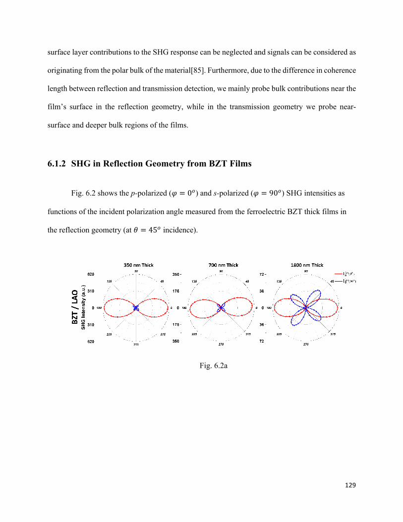
129
surface layer contributions to the SHG response can be neglected and signals can be considered as
originating from the polar bulk of the material[85]. Furthermore, due to the difference in coherence
length between reflection and transmission detection, we mainly probe bulk contributions near the
film’s surface in the reflection geometry, while in the transmission geometry we probe near-
surface and deeper bulk regions of the films.
6.1.2 SHG in Reflection Geometry from BZT Films
Fig. 6.2 shows the p-polarized (𝜑 = 0$) and s-polarized (𝜑 = 90$) SHG intensities as
functions of the incident polarization angle measured from the ferroelectric BZT thick films in
the reflection geometry (at 𝜃 = 45$ incidence).
Fig. 6.2a
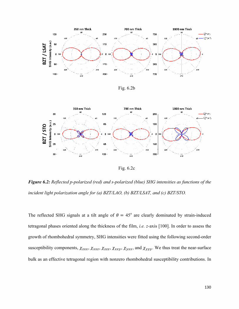
130
Fig. 6.2b
Fig. 6.2c
Figure 6.2: Reflected p-polarized (red) and s-polarized (blue) SHG intensities as functions of the
incident light polarization angle for (a) BZT/LAO, (b) BZT/LSAT, and (c) BZT/STO.
The reflected SHG signals at a tilt angle of 𝜃 = 45o are clearly dominated by strain-induced
tetragonal phases oriented along the thickness of the film, i.e. z-axis [100]. In order to assess the
growth of rhombohedral symmetry, SHG intensities were fitted using the following second-order
susceptibility components, 𝜒GHH, 𝜒HHG, 𝜒GGG, 𝜒HH], 𝜒]HH, and 𝜒]]]. We thus treat the near-surface
bulk as an effective tetragonal region with nonzero rhombohedral susceptibility contributions. In

131
this case, the nonlinear polarization of the probed near-surface bulk region can be expressed as
follows:
𝑃Hb
𝑃]b
𝑃Gb= 2𝜖𝑜
0 0 0 0 𝜒HHG 𝜒HH]𝜒]HH 𝜒]]] 0 𝜒HHG 0 0𝜒GHH 𝜒GHH 𝜒GGG 0 0 0
𝐿𝑥𝑥𝜔 2𝐸𝑥(𝜔)2
𝐿𝑦𝑦𝜔2𝐸𝑦(𝜔)
2
𝐿𝑧𝑧𝜔 2𝐸𝑧(𝜔)2
2𝐿𝑦𝑦𝜔 𝐿𝑧𝑧𝜔 𝐸𝑦(𝜔)𝐸𝑧(𝜔)2𝐿𝑥𝑥𝜔 𝐿𝑧𝑧𝜔 𝐸𝑥(𝜔)𝐸𝑧(𝜔)2𝐿𝑥𝑥𝜔 𝐿𝑦𝑦𝜔 𝐸𝑥(𝜔)𝐸𝑦(𝜔)
(6.1)
The vector components of the nonlinear polarization are then written as:
𝑃H 2𝜔 = 2𝜖𝑜 2𝜒𝑥𝑥𝑧𝐿HH 𝐿GG 𝐸H 𝜔 𝐸G 𝜔 + 2𝜒𝑥𝑥𝑦𝐿HH 𝐿]] 𝐸H 𝜔 𝐸] 𝜔 (6.2a)
𝑃] 2𝜔 = 2𝜖𝑜 𝜒𝑦𝑥𝑥 𝐿HH b𝐸H(𝜔)b + 𝜒𝑦𝑦𝑦 𝐿]]b𝐸](𝜔)b + 2𝜒𝑥𝑥𝑧𝐿]] 𝐿GG 𝐸] 𝜔 𝐸G 𝜔 (6.2b)
𝑃G 2𝜔 = 2𝜖$ 𝜒𝑧𝑥𝑥 𝐿HH b𝐸H(𝜔)b + 𝜒𝑧𝑥𝑥 𝐿]]b𝐸](𝜔)b + 𝜒𝑧𝑧𝑧 𝐿GG b𝐸G(𝜔)b (6.2c)
Using Eq. 4.5, the effective nonlinear susceptibility of the region in the reflection geometry can
be expressed as:
𝜒[))(b) = −𝐿HHb𝑐𝑜𝑠𝜃𝑐𝑜𝑠𝜑Æ 2𝜒𝑥𝑥𝑧𝐿HH 𝐿GG 𝑠𝑖𝑛𝜃𝑐𝑜𝑠𝜃𝑐𝑜𝑠b𝜑 +
2𝜒𝑥𝑥𝑦𝐿HH 𝐿]] 𝑐𝑜𝑠𝜃𝑠𝑖𝑛𝜑𝑐𝑜𝑠𝜑 +𝐿]]b𝑠𝑖𝑛𝜑Æ 𝜒𝑦𝑥𝑥 𝐿HH b𝑐𝑜𝑠b𝜃𝑐𝑜𝑠b𝜑 +
𝜒𝑦𝑦𝑦 𝐿]]b𝑠𝑖𝑛b𝜑 + 2𝜒𝑥𝑥𝑧𝐿]] 𝐿GG 𝑠𝑖𝑛𝜃𝑠𝑖𝑛𝜑𝑐𝑜𝑠𝜑 +
𝐿GGb𝑠𝑖𝑛𝜃𝑐𝑜𝑠𝜑Æ 𝜒𝑧𝑥𝑥 𝐿HH b𝑐𝑜𝑠b𝜃𝑐𝑜𝑠b𝜑 + 𝜒𝑧𝑥𝑥 𝐿]]b𝑠𝑖𝑛b𝜑 +
𝜒𝑧𝑧𝑧 𝐿GG b𝑠𝑖𝑛b𝜃𝑐𝑜𝑠b𝜑
(6.3)
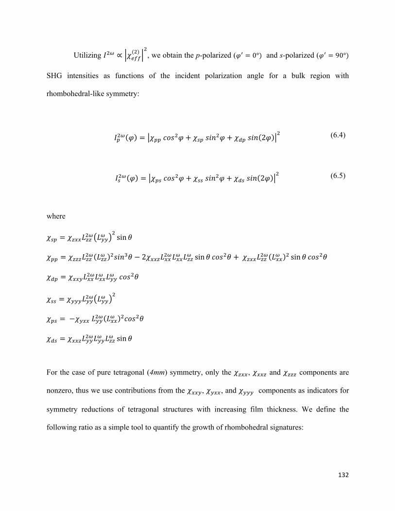
132
Utilizing 𝐼b ∝ 𝜒[))(b) b
, we obtain the p-polarized (𝜑Æ = 0°) and s-polarized (𝜑Æ = 90°)
SHG intensities as functions of the incident polarization angle for a bulk region with
rhombohedral-like symmetry:
𝐼<b 𝜑 = 𝜒<<𝑐𝑜𝑠b𝜑 + 𝜒%<𝑠𝑖𝑛b𝜑 + 𝜒"<𝑠𝑖𝑛 2𝜑 b (6.4)
𝐼%b 𝜑 = 𝜒<%𝑐𝑜𝑠b𝜑 + 𝜒%%𝑠𝑖𝑛b𝜑 + 𝜒"%𝑠𝑖𝑛 2𝜑 b (6.5)
where
𝜒%< = 𝜒GHH𝐿GGb 𝐿]]b sin 𝜃
𝜒<< = 𝜒GGG𝐿GGb 𝐿GG b𝑠𝑖𝑛c𝜃 − 2𝜒HHG𝐿HHb𝐿HH 𝐿GG sin 𝜃 𝑐𝑜𝑠b𝜃 +𝜒GHH𝐿GGb 𝐿HH b sin 𝜃 𝑐𝑜𝑠b𝜃
𝜒"< = 𝜒HH]𝐿HHb𝐿HH 𝐿]] 𝑐𝑜𝑠b𝜃
𝜒%% = 𝜒]]]𝐿]]b 𝐿]]b
𝜒<% = −𝜒]HH𝐿]]b 𝐿HH b𝑐𝑜𝑠b𝜃
𝜒"% = 𝜒HHG𝐿]]b𝐿]] 𝐿GG sin 𝜃
For the case of pure tetragonal (4mm) symmetry, only the 𝜒GHH, 𝜒HHG and 𝜒GGG components are
nonzero, thus we use contributions from the 𝜒HH], 𝜒]HH, and 𝜒]]] components as indicators for
symmetry reductions of tetragonal structures with increasing film thickness. We define the
following ratio as a simple tool to quantify the growth of rhombohedral signatures:

133
0 ì� ì
= ìíîî o ìííí o ìîîíìïîî o ìîîï o ìïïï
(6.6)
The 0 ì� ì
ratio as a function of film thickness for the BZT films is shown in Fig. 6.3.
Figure 6.3: Ratio between rhombohedral and tetragonal susceptibility components as a function
of film thickness for BZT grown on LAO (a = 3.79Å), LSAT (a = 3.87Å), and STO (a =
3.905Å)[34]. SHG signals in the reflection geometry at 𝜃 = 45o are predominantly from tetragonal
phases. Dashed lines show the increasing rhombohedral signature trend.
The data shows that the rhombohedral susceptibility components, 𝜒HH], 𝜒]HH, and 𝜒]]], grow
stronger with increasing film thickness. This demonstrates a lowering of structural symmetry as
strain relaxations occur away from the film-substrate interface, creating more elastic
rhombohedral. The relaxation of strain appears to be strongest for BZT/LAO and weakest for
BZT/STO. This makes sense since the misfit strain between BZT and LAO is the largest (~5.25%),
while the misfit strain between BZT and STO is the lowest (~2.37%).
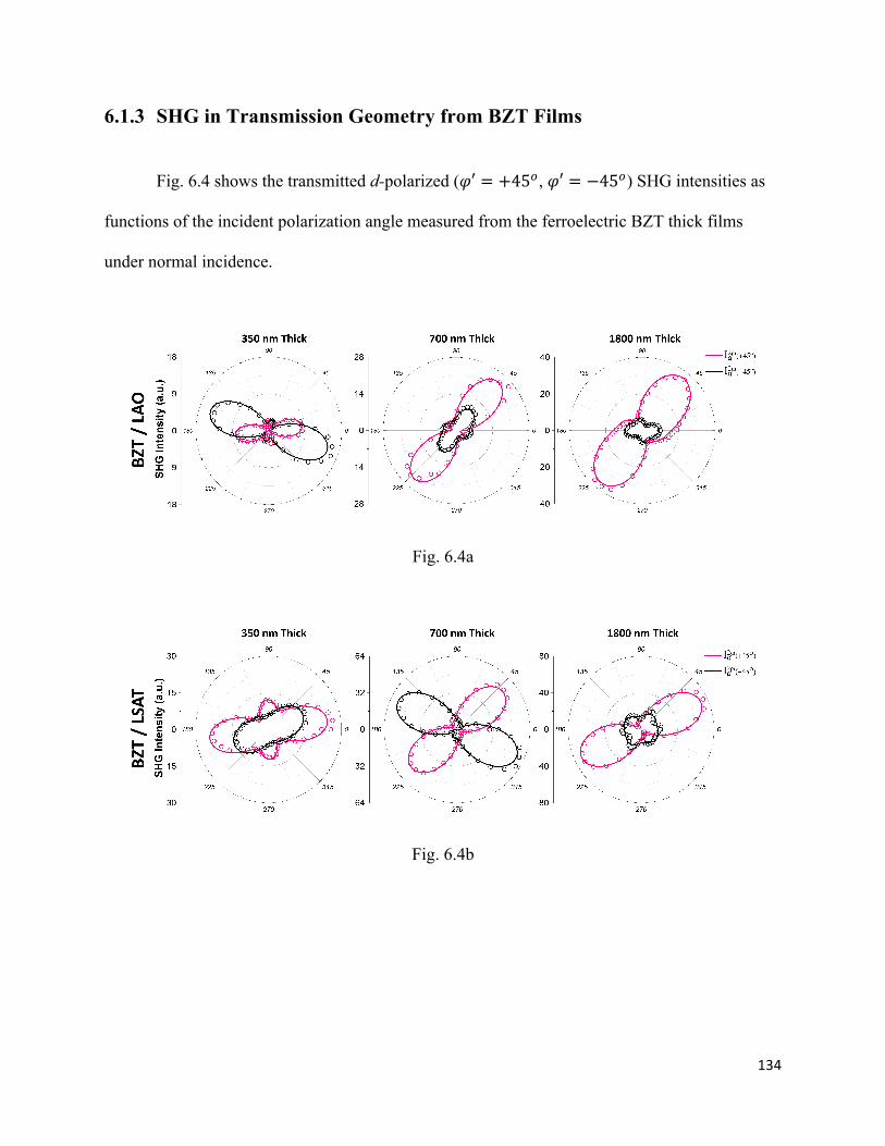
134
6.1.3 SHG in Transmission Geometry from BZT Films
Fig. 6.4 shows the transmitted d-polarized (𝜑′ = +45$, 𝜑′ = −45$) SHG intensities as
functions of the incident polarization angle measured from the ferroelectric BZT thick films
under normal incidence.
Fig. 6.4a
Fig. 6.4b

135
Fig. 6.4c
Figure 6.4: Transmitted d-polarized (𝜑′ = +45$ in pink, 𝜑′ = −45$ in black) SHG intensities
as functions of the incident light polarization angle for (a) BZT/LAO, (b) BZT/LSAT, and (c)
BZT/STO. All SHG intensities were measured under normal incidence.
The transmitted SHG signals with a film tilt angle of 𝜃 = 0o are dominated by elastic rhombohedral
polydomains distributed along the thickness of the film. These domains have effective polarization
orientations with respect to the tetragonal substrate axes, as shown in Fig. 6.5.
Figure 6.5: Rhombohedral domain variants probed in the transmission geometry at normal
incidence. Analyzer orientations for SHG detection are marked above unit cell depictions, i.e. d-
136
polarized (𝜑′ = +45$𝑜𝑟 − 45$). Polarization orientations of each variant are depicted beneath
the unit cells. In total, we have 8 possible rhombohedral domain variants.
In order to fit d-polarized SHG intensities as a function of the incident light polarization angle, the
contribution of each polar domain variant to the nonlinear polarization must be taken into account,
as discussed in detail by Denev et al.[85]. However, in order to take into account incoherent
interference between SHG signals coming from microscale 1st order and nanoscale 2nd order
rhombohedral domains, the d-polarized SHG intensities as functions of the incident polarization
angle were fitted according to the following equation [85, 86]:
𝐼 aaâb 𝜑 = 𝐼a,µb 𝜑 + 𝐼b,µb 𝜑 (6.7a)
𝐼a,µb 𝜑 = 𝐾a,µ(a) 𝑐𝑜𝑠b𝜑 + 𝐾b,µ
(a)𝑠𝑖𝑛b𝜑b+ 𝐾c,µ
(a)𝑠𝑖𝑛b 2𝜑
+ 𝐾p,µ(a) 𝑐𝑜𝑠b𝜑 + 𝐾b,µ
(a)𝑠𝑖𝑛b𝜑 𝑠𝑖𝑛 2𝜑
(6.7b)
𝐼b,µb 𝜑 = 𝐾a,µ(b) 𝑐𝑜𝑠b𝜑 + 𝐾b,µ
(b)𝑠𝑖𝑛b𝜑b+ 𝐾c,µ
(b)𝑠𝑖𝑛b 2𝜑
+ 𝐾p,µ(b) 𝑐𝑜𝑠b𝜑 + 𝐾b,µ
(b)𝑠𝑖𝑛b𝜑 𝑠𝑖𝑛 2𝜑
(6.7c)
For Eq. 6.7, the subscript 𝑗 denotes 𝑥 = 110 or 𝑦 = 110 to designate the analyzer polarization
angle of 𝜑Æ = −45$ or +45$, respectively. In Eq. 6.7a, the total d-polarized SHG intensity is
expressed as an incoherent sum of polarization-resolved SHG intensities from rhombohedral
microdomains and nanodomains throughout the film. Otherwise, most SHG intensity polar plots

137
could not be fitted without violating the important reciprocity condition, 𝐾b,H(6) ∙ 𝐾b,]
6 = 1 [85, 86,
139-144], as discussed by in the model of Denev et al. This condition was held for each set of
fitting coefficients. In Eq. 6.7b and Eq. 6.7c, 𝐾a,H(6) ∝ 𝜒GHH b, 𝐾a,]
(6) ∝ 2𝜒HHG + 𝜒GHH + 2𝜒GGG b,
𝐾b,H(6) = 𝐾b,]
6 ta= bìîîïoìïîîobìïïï
ìïîî, 𝐾c,H
(6) ∝ 𝐾c,](6) ∝ 𝜒HHG b, 𝐾p,H
(6) ∝ 𝜒HHG ∙ 𝜒GHH, and
𝐾p,](6) ∝ 2𝜒HHG + 𝜒GHH + 2𝜒GGG ∙ 𝜒HHG.
Since the d-polarized SHG signals in normal incidence are dominated by rhombohedral
polydomains within a coherence length from the surface of the film, increasing d-SHG intensities
can be used as an indication for the growth of rhombohedral structures due to strain relaxation.
Thus, we use the sum of both d-polarized SHG maxima as a tool for showing the growth of
rhombohedral domains with increasing film thickness, as shown in Fig. 6.6.
Fig. 6.6a Fig. 6.6b
Figure 6.6: (a) sum of maximum d-polarized SHG intensities as a function of film thickness for
BZT grown on LAO (a = 3.79Å)(left scale), LSAT (a = 3.87Å)(right scale), and STO (a =
3.905Å)(right scale)[34]. Dashed lines show the trends for d-SHG intensities to increase with film

138
thickness. (b) Maximum d-polarized SHG intensities plotted as a function of the misfit strain
percent between BZT and the three tetragonal substrates.
A significant degree of inhomogeneity was observed while probing the films in normal incidence,
indicating that the domain distribution can vary depending on the probe site. The data in Fig. 6.6
is in agreement with the data shown in Fig. 6.3. Fig. 6.6 shows that d-SHG signals from
rhombohedral domains is greatest for BZT/ STO, which makes sense since the epitaxial misfit
strain for this film is the lowest of the three substrates. On the other hand, BZT/LAO appears to
have the lowest degree of bulk rhombohedral symmetry, which makes physical sense since the
epitaxial misfit strain for this film is the highest of the three substrates and more strain-induced
tetragonal domains are expected.
6.2 XRD and TEM Results from BZT Films
The SHG results are in good agreement with x-ray diffraction (XRD) and transmission
electron microscopy (TEM) results obtained from the ferroelectric BZT thick films. Fig. 6.7 shows
XRD spectra from the 1800 nm thick BZT film grown on STO. (l00) diffraction peaks were
observed for the SRO electrode and the BZT film, as shown in Fig. 6.7a. The diffraction peaks
show the presence of tetragonal and rhombohedral bulk phases. Fig. 6.7b shows the 𝜙-scan pattern
for the (101) plane of rhombohedral bulk phases. Four strong diffraction peaks with angular
displacements varying between 89.76o and 90.12o depict the pseudo-cubic epitaxial growth of the
BZT film on the STO substrate.
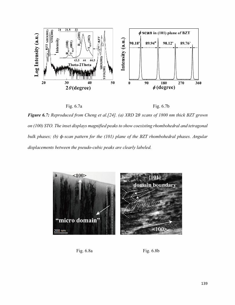
139
Fig. 6.7a
Fig. 6.7b
Figure 6.7: Reproduced from Cheng et al.[24]. (a) XRD 2𝜃 scans of 1800 nm thick BZT grown
on (100) STO. The inset displays magnified peaks to show coexisting rhombohedral and tetragonal
bulk phases; (b) 𝜙-scan pattern for the (101) plane of the BZT rhombohedral phases. Angular
displacements between the pseudo-cubic peaks are clearly labeled.
Fig. 6.8a
Fig. 6.8b

140
Figure 6.8: Reproduced from Cheng et al.[24]. (a) Cross-sectional bright field TEM image of an
1800 nm thick BZT film. The image shows vertical, or columnar, rhombohedral microdomains
along the thickness of the film; (b) Magnified TEM images of domain morphologies in a 700 nm
thick BZT film. Displays [101] domain walls between the nanodomains residing within the [100]
microdomains.
Tetragonal and rhombohedral domain walls are visible in the TEM images for 1800 and 700
nm thick BZT grown on STO. Both 1st order and 2nd order domain structures are shown in Fig.
6.8a and Fig. 6.8b, respectively. The images clearly depict a growth of columnar microdomains
along the thickness of the film. Nanoscale 2nd order rhombohedral domains, marked by their
domain walls, were observed to be imbedded within the vertical microdomains. The presence of
both rhombohedral microdomains and nanodomains in the TEM images can account for the
complex transmitted SHG profiles. Eq. 6.7 would thus represent the incoherent sum of SHG
intensities arising from microscale and nanoscale rhombohedral structures.
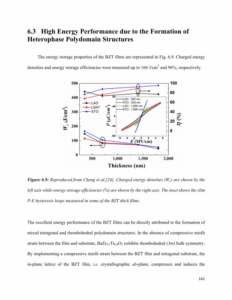
141
6.3 High Energy Performance due to the Formation of Heterophase Polydomain Structures
The energy storage properties of the BZT films are represented in Fig. 6.9. Charged energy
densities and energy storage efficiencies were measured up to 166 J/cm3 and 96%, respectively.
Figure 6.9: Reproduced from Cheng et al.[24]. Charged energy densities (Wc) are shown by the
left axis while energy storage efficiencies (%) are shown by the right axis. The inset shows the slim
P-E hysteresis loops measured in some of the BZT thick films.
The excellent energy performance of the BZT films can be directly attributed to the formation of
mixed tetragonal and rhombohedral polydomain structures. In the absence of compressive misfit
strain between the film and substrate, BaZr0.2Ti0.8O3 exhibits rhombohedral (3m) bulk symmetry.
By implementing a compressive misfit strain between the BZT film and tetragonal substrate, the
in-plane lattice of the BZT film, i.e. crystallographic ab-plane, compresses and induces the
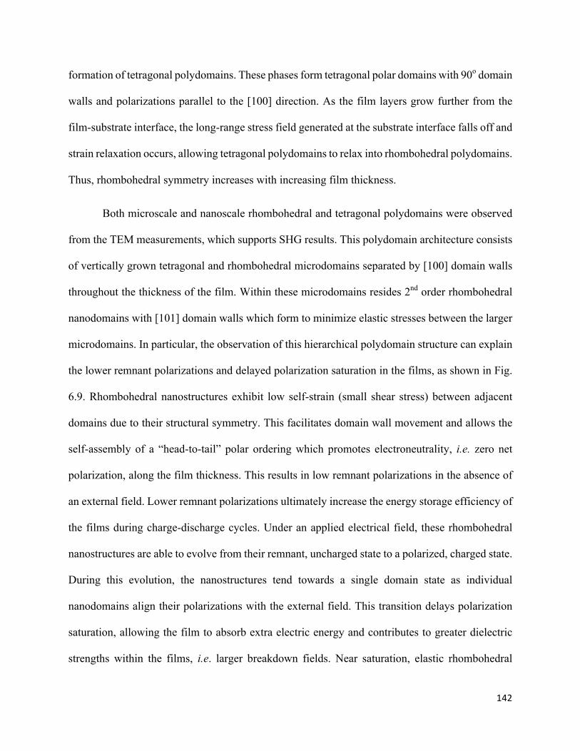
142
formation of tetragonal polydomains. These phases form tetragonal polar domains with 90o domain
walls and polarizations parallel to the [100] direction. As the film layers grow further from the
film-substrate interface, the long-range stress field generated at the substrate interface falls off and
strain relaxation occurs, allowing tetragonal polydomains to relax into rhombohedral polydomains.
Thus, rhombohedral symmetry increases with increasing film thickness.
Both microscale and nanoscale rhombohedral and tetragonal polydomains were observed
from the TEM measurements, which supports SHG results. This polydomain architecture consists
of vertically grown tetragonal and rhombohedral microdomains separated by [100] domain walls
throughout the thickness of the film. Within these microdomains resides 2nd order rhombohedral
nanodomains with [101] domain walls which form to minimize elastic stresses between the larger
microdomains. In particular, the observation of this hierarchical polydomain structure can explain
the lower remnant polarizations and delayed polarization saturation in the films, as shown in Fig.
6.9. Rhombohedral nanostructures exhibit low self-strain (small shear stress) between adjacent
domains due to their structural symmetry. This facilitates domain wall movement and allows the
self-assembly of a “head-to-tail” polar ordering which promotes electroneutrality, i.e. zero net
polarization, along the film thickness. This results in low remnant polarizations in the absence of
an external field. Lower remnant polarizations ultimately increase the energy storage efficiency of
the films during charge-discharge cycles. Under an applied electrical field, these rhombohedral
nanostructures are able to evolve from their remnant, uncharged state to a polarized, charged state.
During this evolution, the nanostructures tend towards a single domain state as individual
nanodomains align their polarizations with the external field. This transition delays polarization
saturation, allowing the film to absorb extra electric energy and contributes to greater dielectric
strengths within the films, i.e. larger breakdown fields. Near saturation, elastic rhombohedral

143
nanodomains behave like tetragonal ones, however, the electrical field is unable to fully overpower
the elastic interactions between domains and the film does not completely saturate. During the
discharging process, these rhombohedral nanostructures are able to fully relax back to their
remnant, multi-domain state as the external field approaches zero[31].
6.4 Summary
A rhombohedral BaZr0.2Ti0.8O3 (BZT) solid solution was combined with a compressive film-
substrate misfit strain to engineer heterophase polydomain structures in BZT ferroelectric films.
High energy storage densities (up to 166 J/cm3) and efficiencies (up to 96 %) were obtained with
excellent field and frequency stabilities. Polarization-resolved SHG intensities were measured in
the reflection and transmission geometries to study mixed tetragonal and rhombohedral phases in
the epitaxially strained BZT thick films. Reflected SHG intensities measured at 45o incidence from
near-surface domains show the growth of rhombohedral symmetry with increasing film thickness.
Transmitted SHG intensities measured at normal incidence from deeper bulk domains also
demonstrate the growth of rhombohedral symmetry with increasing film thickness. All
observations are associated with structural symmetry reductions as strain-induced tetragonal
domains transition into elastic rhombohedral polydomains. This symmetry reduction is explained
by the relaxation of strain away from the film-substrate interface. The SHG results are consistent
with those from XRD and TEM measurements, revealing the coexistence of tetragonal
microstructures and rhombohedral nanostructures as elastic domains in the compressively strained
films. The excellent energy storage performance of these films is a direct result of the formation
of these heterophase polydomain structures which can be tuned using substrate strain and thickness
scaling effects.

144
Chapter 7: Summary and Outlook
7.1 General Summary
We have studied local structural changes due to the dc electric field-induced migration of
oxygen vacancies at Fe:STO single crystal interfaces, oxygen vacancy migration-induced
structural defect and strain formation in electrodegraded Fe:STO single crystals, and mixed
tetragonal and rhombohedral phases in ferroelectric BZT thick films.
First, we investigated local structural changes due to the dc electric field-driven migration
of oxygen vacancies at Fe:STO single crystal interfaces using optical SHG and photoluminescence
measurements. Field-induced ionic displacements were detected by changes in the susceptibility
components of the tetragonal interfaces as a result of electrostrictive distortions. These distortions
were described in detail according to Fe:Ti-O bond stretching and bending effects within the Fe:Ti-
O6 octahedron. Differences in the nonlinear responses between the oxidized and reduced sample
interfaces studied were explained by their respective Schottky barriers and built-in electric fields.
The built-in electric field at the interfacial depletion region is revealed to be greater in oxidized
Fe:STO compared to reduced Fe:STO, providing strong evidence that oxygen vacancies contribute
to lower Schottky energy barrier heights as well as thinner depletion regions. This facilitates
stronger structural changes at low dc voltages in the reduced crystal compared to the oxidized one.
Moreover, structural differences between the reduced and oxidized Fe:STO cathodes are indicated
by the EFISHG and photoluminescence results, showing that a clustering and straining of oxygen
145
vacancy defects at the reduced cathode occurs. This effect breaks in-plane isotropies and the
reduced cathode interface deviates from tetragonal (4mm) symmetry.
Next, we investigated structural defect and strain formation in electrodegraded reduced and
oxidized Fe:STO single crystals using optical SHG and confocal Raman spectroscopy. SHG
revealed high degrees of structural inhomogeneity across degraded anode and cathode interfaces
which were explained by the formation of Fe4+/oxygen ion and Fe3+/oxygen vacancy aggregation
sites, respectively. We have also shown that mixed Fe3+/Fe4+ states and strain form along the
electrocoloration boundaries in both single crystals. This, as well as oxygen sublattice variations
between the anodic and cathodic bulk shown by confocal Raman data, demonstrates that oxygen
vacancy demixing generates a structural interface along the color front. In comparing both
electrodegraded oxidized and reduced Fe:STO crystals, we reveal that strain is greater across the
oxidized crystal’s color front compared to the reduced crystal, although the strained region is
slightly wider in the reduced crystal. Our results indicate that structural and electrochemical
inhomogeneity has a dependence on the distance between electrodes due to the finite size (~0.3–
0.58 mm) of the strain field which forms across electrocoloration boundaries.
Lastly, we employed polarization-resolved SHG in the reflection and transmission
geometries to investigate heterophase polydomain structures in compressively strained
ferroelectric BZT thick films. These films exhibit high energy storage densities and efficiencies
showcased by their slim, pseudo-linear P-E hysteresis loops. In the reflection geometry, the SHG
intensity is dominated by contributions from strain-induced tetragonal microdomains growing
along the thickness of the film. In the transmission geometry, SHG contributions from tetragonal
structures are suppressed and the signal arises from rhombohedral polydomains. SHG results
demonstrated the growth of rhombohedral symmetry with increasing film thickness, explained by
146
strain relaxation away from the tetragonal film-substrate interface. Greater misfit strains between
the BZT films and substrates were shown to lead to a higher degree of tetragonal symmetry. In
addition, the presence of mixed rhombohedral and tetragonal phases was supported by
transmission electron microscopy (TEM) and x-ray diffraction (XRD) measurements which
verified the growth of columnar [100] tetragonal microdomains with [101] rhombohedral
nanodomains imbedded within them. The high energy performance of the films is well explained
by these mixed tetragonal and rhombohedral polydomain structures which serve to decrease
remnant polarizations and delay polarization saturation.
7.2 Outlook and Future Experiments
Our investigation of structural defect and strain formation resulting from the dc electric
field-induced migration of oxygen vacancies in pristine and electrodegraded Fe:STO single
crystals yielded valuable insights into dc electric field-induced dielectric breakdown mechanisms.
One significant insight is the competition between the conservation of electroneutrality and
structural strain formation. Just as oxygen vacancies form in order to conserve charge neutrality
within the perovskite unit cell, oxygen vacancy demixing occurs in order to conserve
electroneutrality in the dielectric’s bulk with respect to the external electrical field. This migratory
process, as we have shown, results in strain formation between anodic and cathodic bulk regions,
i.e. across electrocoloration boundaries. Furthermore, dc electric stress-induced electrostriction
also results in structural strain. Strain resulting from external dc electrical fields and ionic defect
accumulation should not be ignored when modeling conductivity changes to describe voltage-
induced resistance degradation, especially in ferroelectric ceramics where electrical and
mechanical properties are strongly coupled. Structural strain serves to promote oxygen vacancy
147
migration by lowering migration enthalpies, compromising bond strengths, and generating defect
states [70, 71, 145]. In the future, elasticity changes across electrodegraded dielectric ceramics
may be investigated using coherent longitudinal acoustic phonon spectroscopy. In addition, the
field-induced structural evolution of electrocoloration boundaries may also be probed in real-time
using optical SHG as a direct continuation of this study. Furthermore, oxygen vacancy migration-
induced structural changes should be examined in perovskite dielectrics with different chemical
compositions to gain further understandings.
Our study of coexisting tetragonal and rhombohedral phases as elastic polydomain
structures in ferroelectric BZT thick films has also helped provide significant insights into the
strain engineering of heterophase polydomain structures for high energy performance. We have
probed remnant polydomain structures in these films, however, electric field-induced polydomain
evolutions would yield even more valuable structural insights. In the future, electric field-induced
structural changes of these mixed tetragonal and rhombohedral polydomain structures can be
investigated using optical SHG in the reflection and transmission geometries as well as confocal
Raman spectroscopy. Near-field SHG microscopy, with or without voltage, would allow a direct
imaging of polar domain morphologies within the films. Furthermore, field-dependent coherent
longitudinal acoustic phonon spectroscopy can be performed to investigate structural changes in
epitaxially strained films. Finally, since the stabilization of heterophase polydomain structures
relies heavily on the long-range stress field generated at the substrate interface and chemical
composition of the film, combinations of different compositions and substrate species may be
probed using various nonlinear optical techniques, such as optical SHG and confocal Raman
spectroscopy.
148
Bibliography
[1] X. Hao, A review on the dielectric materials for high energy-storage application, Journal of Advanced Dielectrics 3(01) (2013) 1330001.
[2] P.S. Peercy, The drive to miniaturization, Nature 406(6799) (2000) 1023-1027.
[3] G.E. Moore, Cramming more components onto integrated circuits, Proceedings of the IEEE 86(1) (1998) 82-85.
[4] J.-J. Wang, H.-B. Huang, T.J. Bayer, A. Moballegh, Y. Cao, A. Klein, E.C. Dickey, D.L. Irving, C.A. Randall, L.-Q. Chen, Defect chemistry and resistance degradation in Fe-doped SrTiO 3 single crystal, Acta Materialia 108 (2016) 229-240.
[5] R. Waser, T. Baiatu, K.H. Härdtl, dc Electrical Degradation of Perovskite- Type Titanates: I, Ceramics, Journal of the American Ceramic Society 73(6) (1990) 1645-1653.
[6] R. Waser, T. Baiatu, K.H. Härdtl, dc Electrical Degradation of Perovskite- Type Titanates: II, Single Crystals, Journal of the American Ceramic Society 73(6) (1990) 1654-1662.
[7] T. Baiatu, R. Waser, K.H. Härdtl, dc Electrical Degradation of Perovskite- Type Titanates: III, A Model of the Mechanism, Journal of the American Ceramic Society 73(6) (1990) 1663-1673.
[8] W. Liu, G.Y. Yang, C.A. Randall, Evidence for Increased Polaron Conduction Near the Cathodic Interface in the Final Stages of Electrical Degradation in SrTiO3 Crystals, Japanese Journal of Applied Physics 48(5R) (2009) 051404.
[9] T.J.M. Bayer, J.J. Wang, J.J. Carter, A. Moballegh, J. Baker, D.L. Irving, E.C. Dickey, L.Q. Chen, C.A. Randall, The relation of electrical conductivity profiles and modulus data using the example of STO: Fe single crystals: A path to improve the model of resistance degradation, Acta Materialia 117 (2016) 252-261.
[10] J.J. Wang, H.B. Huang, T.J.M. Bayer, A. Moballegh, Y. Cao, A. Klein, E.C. Dickey, D.L. Irving, C.A. Randall, L.Q. Chen, Defect chemistry and resistance degradation in Fe-doped SrTiO3 single crystal, Acta Materialia 108 (2016) 229-240.

149
[11] G.Y. Yang, E.C. Dickey, C.A. Randall, M.S. Randall, L.A. Mann, Modulated and ordered defect structures in electrically degraded Ni–BaTiO3 multilayer ceramic capacitors, Journal of applied physics 94(9) (2003) 5990-5996.
[12] R. Merkle, J. Maier, How Is Oxygen Incorporated into Oxides? A Comprehensive Kinetic Study of a Simple Solid- State Reaction with SrTiO3 as a Model Material, Angewandte Chemie International Edition 47(21) (2008) 3874-3894.
[13] G.Y. Yang, E.C. Dickey, C.A. Randall, D.E. Barber, P. Pinceloup, M.A. Henderson, R.A. Hill, J.J. Beeson, D.J. Skamser, Oxygen nonstoichiometry and dielectric evolution of BaTiO3. Part I—improvement of insulation resistance with reoxidation, Journal of Applied Physics 96(12) (2004) 7492-7499.
[14] G.Y. Yang, G.D. Lian, E.C. Dickey, C.A. Randall, D.E. Barber, P. Pinceloup, M.A. Henderson, R.A. Hill, J.J. Beeson, D.J. Skamser, Oxygen nonstoichiometry and dielectric evolution of BaTiO3. Part II—insulation resistance degradation under applied dc bias, Journal of applied physics 96(12) (2004) 7500-7508.
[15] R.A. Maier, C.A. Randall, Low Temperature Ionic Conductivity of an Acceptor- Doped Perovskite: II. Impedance of Single- Crystal BaTiO3, Journal of the American Ceramic Society 99(10) (2016) 3360-3366.
[16] R.A. Maier, C.A. Randall, Low- Temperature Ionic Conductivity of an Acceptor- Doped Perovskite: I. Impedance of Single- Crystal SrTiO3, Journal of the American Ceramic Society (2016).
[17] S. Rodewald, J. Fleig, J. Maier, Resistance Degradation of Iron- Doped Strontium Titanate Investigated by Spatially Resolved Conductivity Measurements, Journal of the American Ceramic Society 83(8) (2000) 1969-1976.
[18] W. Liu, C.A. Randall, Thermally Stimulated Relaxation in Fe- Doped SrTiO3 Systems: I. Single Crystals, Journal of the American Ceramic Society 91(10) (2008) 3245-3250.
[19] W. Liu, C.A. Randall, Thermally Stimulated Relaxation in Fe- Doped SrTiO3 Systems: II. Degradation of SrTiO3 Dielectrics, Journal of the American Ceramic Society 91(10) (2008) 3251-3257.
[20] M. Wojtyniak, K. Szot, R. Wrzalik, C. Rodenbücher, G. Roth, R. Waser, Electro-degradation and resistive switching of Fe-doped SrTiO3 single crystal, Journal of Applied Physics 113(8) (2013) 083713.
150
[21] A. Moballegh, E.C. Dickey, Electric-field-induced point defect redistribution in single-crystal TiO2–x and effects on electrical transport, Acta Materialia 86 (2015) 352-360.
[22] D.G. Schlom, L.Q. Chen, C.B. Eom, K.M. Rabe, S.K. Streiffer, J.M. Triscone, Strain tuning of ferroelectric thin films, Annu. Rev. Mater. Res. 37 (2007) 589-626.
[23] M.D. Hanwell, D.E. Curtis, D.C. Lonie, T. Vandermeersch, E. Zurek, G.R. Hutchison, Avogadro: an advanced semantic chemical editor, visualization, and analysis platform, Journal of cheminformatics 4(1) (2012) 17.
[24] H. Cheng, Y.X. Zhang, D. Ascienzo, Y. Li, Y.Y. Zhao, Y.H. Ren, J. Ouyang, Demonstration of Ultra-high Recyclable Energy Densities in Domain-Engineered Ferroelectric Films, Nature communications (under review) (2017).
[25] B. Chu, X. Zhou, K. Ren, B. Neese, M. Lin, Q. Wang, F. Bauer, Q.M. Zhang, A dielectric polymer with high electric energy density and fast discharge speed, Science 313(5785) (2006) 334-336.
[26] S. Tong, B. Ma, M. Narayanan, S. Liu, R. Koritala, U. Balachandran, D. Shi, Lead lanthanum zirconate titanate ceramic thin films for energy storage, ACS applied materials & interfaces 5(4) (2013) 1474-1480.
[27] B. Peng, Q. Zhang, X. Li, T. Sun, H. Fan, S. Ke, M. Ye, Y. Wang, W. Lu, H. Niu, Giant Electric Energy Density in Epitaxial Lead- Free Thin Films with Coexistence of Ferroelectrics and Antiferroelectrics, Advanced Electronic Materials 1(5) (2015).
[28] W. Zhang, Y. Gao, L. Kang, M. Yuan, Q. Yang, H. Cheng, W. Pan, J. Ouyang, Space-charge dominated epitaxial BaTiO3 heterostructures, Acta Materialia 85 (2015) 207-215.
[29] Z. Sun, C. Ma, M. Liu, J. Cui, L. Lu, J. Lu, X. Lou, L. Jin, H. Wang, C.L. Jia, Ultrahigh Energy Storage Performance of Lead- Free Oxide Multilayer Film Capacitors via Interface Engineering, Advanced Materials (2016).
[30] M. McMillen, A.M. Douglas, T.M. Correia, P.M. Weaver, M.G. Cain, J.M. Gregg, Increasing recoverable energy storage in electroceramic capacitors using “dead-layer” engineering, Applied Physics Letters 101(24) (2012) 242909.
[31] A.L. Roytburd, J. Ouyang, A. Artemev, Polydomain structures in ferroelectric and ferroelastic epitaxial films, Journal of Physics: Condensed Matter 29(16) (2017) 163001.

151
[32] A.L. Roytburd, Thermodynamics of polydomain heterostructures. I. Effect of macrostresses, Journal of applied physics 83(1) (1998) 228-238.
[33] A.L. Roytburd, Thermodynamics of polydomain heterostructures. II. Effect of microstresses, Journal of applied physics 83(1) (1998) 239-245.
[34] R.J. Zeches, M.D. Rossell, J.X. Zhang, A.J. Hatt, Q. He, C.H. Yang, A. Kumar, C.H. Wang, A. Melville, C. Adamo, A strain-driven morphotropic phase boundary in BiFeO3, science 326(5955) (2009) 977-980.
[35] W. Zhang, J. Ouyang, A.L. Roytburd, Effect of thickness-mediated misfit strain on the heterophase polydomain structure of epitaxial BiFeO3 films, Scripta Materialia 66(7) (2012) 499-502.
[36] J.H. Cho, K.C. Park, Comparison of epitaxial growth of PbZr0.53Ti0.47O3 on SrRuO3 and La0.5Sr0.5CoO3, Applied physics letters 75(4) (1999) 549-551.
[37] M. Fiebig, V.V. Pavlov, R.V. Pisarev, Second-harmonic generation as a tool for studying electronic and magnetic structures of crystals: review, JOSA B 22(1) (2005) 96-118.
[38] R. Newnham, V. Sundar, R. Yimnirun, J. Su, Q. Zhang, Electrostriction: nonlinear electromechanical coupling in solid dielectrics, The Journal of Physical Chemistry B 101(48) (1997) 10141-10150.
[39] R.W. Boyd, Nonlinear optics, Academic press2003.
[40] E. Vlahos, Phase transitions and domain structures in multiferroics, The Pennsylvania State University2011.
[41] P.R. Potnis, N.T. Tsou, J.E. Huber, A review of domain modelling and domain imaging techniques in ferroelectric crystals, Materials 4(2) (2011) 417-447.
[42] A.S. Bhalla, R. Guo, R. Roy, The perovskite structure—a review of its role in ceramic science and technology, Materials Research Innovations 4(1) (2000) 3-26.
[43] V.M. Goldschmidt, Crystal structure and chemical correlation, Ber. Dtsch. Chem. Ges 60 (1927) 1263-1296.
152
[44] R.A. Maier, Dynamics of oxygen vacancies and defect complexes in the perovskite oxide structure, The Pennsylvania State University2014.
[45] R.D.T. Shannon, C.T. Prewitt, Effective ionic radii in oxides and fluorides, Acta Crystallographica Section B: Structural Crystallography and Crystal Chemistry 25(5) (1969) 925-946.
[46] D.J. Meyers, Engineering the Ground State of Complex Oxides, Theses and Dissertations. 1289 (2015).
[47] W. Travis, E.N.K. Glover, H. Bronstein, D.O. Scanlon, R.G. Palgrave, On the application of the tolerance factor to inorganic and hybrid halide perovskites: a revised system, Chemical Science 7(7) (2016) 4548-4556.
[48] C. Lenser, A. Kalinko, A. Kuzmin, D. Berzins, J. Purans, K. Szot, R. Waser, R. Dittmann, Spectroscopic study of the electric field induced valence change of Fe-defect centers in SrTiO3, Physical Chemistry Chemical Physics 13(46) (2011) 20779-20786.
[49] T.H. Hölbling, N. Söylemezoğlu, R. Waser, A Mathematical-Physical Model for the Charge Transport in p-Type SrTiO3 Ceramics Under dc Load: Maxwell-Wagner Relaxation, Journal of electroceramics 9(2) (2002) 87-100.
[50] R.A. De Souza, J. Fleig, R. Merkle, J. Maier, SrTiO3: A Model Electroceramic: Dedicated to Professor Dr. Dr. hc Manfred Rühle on the Occasion of his 65th Birthday, Zeitschrift für Metallkunde 94(3) (2003) 218-225.
[51] I. Denk, W. Münch, J. Maier, Partial Conductivities in SrTiO3: Bulk Polarization Experiments, Oxygen Concentration Cell Measurements, and Defect- Chemical Modeling, Journal of the American Ceramic Society 78(12) (1995) 3265-3272.
[52] D.M. Smyth, The defect chemistry of metal oxides, The Defect Chemistry of Metal Oxides, by DM Smyth, pp. 304. Foreword by DM Smyth. Oxford University Press, Jun 2000. ISBN-10: 0195110145. ISBN-13: 9780195110142 (2000) 304.
[53] R.A. De Souza, Oxygen diffusion in SrTiO3 and related perovskite oxides, Advanced Functional Materials 25(40) (2015) 6326-6342.

153
[54] M. Schie, R. Waser, R.A. De Souza, A simulation study of oxygen-vacancy behavior in strontium titanate: beyond nearest-neighbor interactions, The Journal of Physical Chemistry C 118(28) (2014) 15185-15192.
[55] R.A. De Souza, V. Metlenko, D. Park, T.E. Weirich, Behavior of oxygen vacancies in single-crystal SrTiO3: Equilibrium distribution and diffusion kinetics, Physical Review B 85(17) (2012) 174109.
[56] R. Herger, P.R. Willmott, O. Bunk, C.M. Schlepütz, B.D. Patterson, B. Delley, Surface of strontium titanate, Physical review letters 98(7) (2007) 076102.
[57] R.Q. Zhao, K.J. Jin, H.Z. Guo, H.B. Lu, G.Z. Yang, A study on surface symmetry and interfacial enhancement of SrTiO3 by second harmonic generation, Science China Physics, Mechanics and Astronomy 56(12) (2013) 2370-2376.
[58] V.E. Alexandrov, J. Maier, R.A. Evarestov, Ab initio study of SrFexTi1− xO3: Jahn-Teller distortion and electronic structure, Physical Review B 77(7) (2008) 075111.
[59] M. Vracar, A. Kuzmin, R. Merkle, J. Purans, E.A. Kotomin, J. Maier, O. Mathon, Jahn-Teller distortion around Fe4+ in Sr(FexTi1− x)O3−δ from X-ray absorption spectroscopy, X-ray diffraction, and vibrational spectroscopy, Physical Review B 76(17) (2007) 174107.
[60] R.A. Maier, T.A. Pomorski, P.M. Lenahan, C.A. Randall, Acceptor-oxygen vacancy defect dipoles and fully coordinated defect centers in a ferroelectric perovskite lattice: Electron paramagnetic resonance analysis of Mn2+ in single crystal BaTiO3, Journal of Applied Physics 118(16) (2015) 164102.
[61] J. Kwon, A.A. Sharma, J.A. Bain, Y.N. Picard, M. Skowronski, Oxygen vacancy creation, drift, and aggregation in TiO2- based resistive switches at low temperature and voltage, Advanced Functional Materials 25(19) (2015) 2876-2883.
[62] C.A. Randall, R. Maier, W. Qu, K. Kobayashi, K. Morita, Y. Mizuno, N. Inoue, T. Oguni, Improved reliability predictions in high permittivity dielectric oxide capacitors under high dc electric fields with oxygen vacancy induced electromigration, Journal of Applied Physics 113(1) (2013) 014101.
[63] H. Neumann, G. Arlt, Maxwell-wagner relaxation and degradation of SrTiO3 and BaTiO3 ceramics, Ferroelectrics 69(1) (1986) 179-186.

154
[64] J.N. Baker, P.C. Bowes, D.M. Long, A. Moballegh, J.S. Harris, E.C. Dickey, D.L. Irving, Defect mechanisms of coloration in Fe-doped SrTiO3 from first principles, Applied Physics Letters 110(12) (2017) 122903.
[65] J. Blanc, D.L. Staebler, Electrocoloration in SrTiO3: Vacancy drift and oxidation-reduction of transition metals, Physical Review B 4(10) (1971) 3548.
[66] D. Ascienzo, H. Yuan, S. Greenbaum, T.J.M. Bayer, R.A. Maier, J.J. Wang, C.A. Randall, E.C. Dickey, H. Zhao, Y.H. Ren, Investigation of Electric Field–Induced Structural Changes at Fe-Doped SrTiO3 Anode Interfaces by Second Harmonic Generation, Materials 9(11) (2016) 883.
[67] H.Y. Lee, Y. Peng, Y.M. Shkel, Strain-dielectric response of dielectrics as foundation for electrostriction stresses, Journal of Applied Physics 98(7) (2005) 074104.
[68] V. Sundar, R.E. Newnham, Electrostriction and polarization, Ferroelectrics 135(1) (1992) 431-446.
[69] X. Zhao, Z. Suo, Electrostriction in elastic dielectrics undergoing large deformation, Journal of Applied Physics 104(12) (2008) 123530.
[70] B. Yildiz, “Stretching” the energy landscape of oxides—Effects on electrocatalysis and diffusion, Mrs Bulletin 39(02) (2014) 147-156.
[71] T. Mayeshiba, D. Morgan, Strain effects on oxygen migration in perovskites, Phys. Chem. Chem. Phys. 17(4) (2014) 2715-2721.
[72] J. Hanzig, M. Zschornak, F. Hanzig, E. Mehner, H. Stöcker, B. Abendroth, C. Röder, A. Talkenberger, G. Schreiber, D. Rafaja, Migration-induced field-stabilized polar phase in strontium titanate single crystals at room temperature, Physical Review B 88(2) (2013) 024104.
[73] M. Brack, The physics of simple metal clusters: self-consistent jellium model and semiclassical approaches, Reviews of modern physics 65(3) (1993) 677.
[74] P.F. Brevet, Surface second harmonic generation, PPUR presses polytechniques1997.
[75] A. Marchewka, D. Cooper, C. Lenser, S. Menzel, H. Du, R. Dittmann, R.E. Dunin-Borkowski, R. Waser, Determination of the electrostatic potential distribution in

155
Pt/Fe:SrTiO3/Nb:SrTiO3 thin-film structures by electron holography, Scientific Reports 4 (2014) 6975.
[76] J.L. Freeouf, J.M. Woodall, Schottky barriers: An effective work function model, Electronic Structure of Metal-Semiconductor Contacts, Springer1990, pp. 154-156.
[77] S.P. Alpay, A.L. Roytburd, Thermodynamics of polydomain heterostructures. III. Domain stability map, Journal of Applied Physics 83(9) (1998) 4714-4723.
[78] J.B. MacChesney, P.K. Gallagher, F.V. DiMarcello, Stabilized barium titanate ceramics for capacitor dielectrics, Journal of the American Ceramic Society 46(5) (1963) 197-202.
[79] Y. Li, H. Cheng, H. Xu, Y. Zhang, P. Yan, T. Huang, C. Wang, Z. Hu, J. Ouyang, Electromechanical properties of (Ba, Sr)(Zr, Ti)O3 ceramics, Ceramics International 42(8) (2016) 10191-10196.
[80] J. Ouyang, A.L. Roytburd, Theoretical modeling of coexisting tetragonal and rhombohedral heterophase polydomain structures in lead zirconate titanate ferroelectric films near the morphotropic phase boundary, Acta materialia 54(20) (2006) 5565-5572.
[81] S.W. Liu, S. Jolly, M. Xiao, Z. Yuan, J. Liu, C. Chen, W. Zhu, Domain microstructures and ferroelectric phase transition in Pb0.35Sr0.65TiO3 films studied by second harmonic generation in reflection geometry, Journal of applied physics 101(10) (2007) 104118.
[82] E.D. Mishina, T.V. Misuryaev, N.E. Sherstyuk, V.V. Lemanov, A.I. Morozov, A.S. Sigov, T. Rasing, Observation of a near-surface structural phase transition in SrTiO3 by optical second harmonic generation, Physical review letters 85(17) (2000) 3664.
[83] L.D. Rotter, D.L. Kaiser, Detection of internal electric fields in BaTiO3 thin films by optical second harmonic generation, Integrated Ferroelectrics 22(1-4) (1998) 153-170.
[84] Y.R. Shen, Principles of nonlinear optics, (1984).
[85] S.A. Denev, T.T.A. Lummen, E. Barnes, A. Kumar, V. Gopalan, Probing ferroelectrics using optical second harmonic generation, Journal of the American Ceramic Society 94(9) (2011) 2699-2727.

156
[86] A. Kumar, S. Denev, R.J. Zeches, E. Vlahos, N.J. Podraza, A. Melville, D.G. Schlom, R. Ramesh, V. Gopalan, Probing mixed tetragonal/rhombohedral-like monoclinic phases in strained bismuth ferrite films by optical second harmonic generation, Applied Physics Letters 97(11) (2010) 112903.
[87] J.J.H. Gielis, P.M. Gevers, I.M.P. Aarts, M.C.M. Van De Sanden, W.M.M. Kessels, Optical second-harmonic generation in thin film systems, Journal of Vacuum Science & Technology A 26(6) (2008) 1519-1537.
[88] J.D. Jackson, Classical electrodynamics, John Wiley & Sons2007.
[89] P.W. Smith, Mode-locking of lasers, Proceedings of the IEEE 58(9) (1970) 1342-1357.
[90] H.A. Haus, Mode-locking of lasers, IEEE Journal of Selected Topics in Quantum Electronics 6(6) (2000) 1173-1185.
[91] K. WALL, A. Sanchez, Titanium sapphire lasers, The Lincoln laboratory journal 3(3) (1990) 447-462.
[92] S.A. Self, Focusing of spherical Gaussian beams, Applied optics 22(5) (1983) 658-661.
[93] M. Born, E. Wolf, Principles of optics: electromagnetic theory of propagation, interference and diffraction of light, Elsevier2013.
[94] M.J. Weber, CRC handbook of laser science and Technology supplement 2: optical materials, CRC press1994.
[95] S.H. Wemple, M. Didomenico, I. Camlibel, Dielectric and optical properties of melt-grown BaTiO3, Journal of Physics and Chemistry of Solids 29(10) (1968) 1797-1803.
[96] X. Zhuang, P.B. Miranda, D. Kim, Y.R. Shen, Mapping molecular orientation and conformation at interfaces by surface nonlinear optics, Physical Review B 59(19) (1999) 12632.
[97] Y.R. Shen, Optical second harmonic generation at interfaces, Annual Review of Physical Chemistry 40(1) (1989) 327-350.
[98] A. Rubano, M. Fiebig, D. Paparo, A. Marino, D. Maccariello, U. ScottidiUccio, F. MilettoGranozio, L. Marrucci, C. Richter, S. Paetel, J. Mannhart, Spectral and spatial

157
distribution of polarization at the LaAlO3/SrTiO3 interface, Physical Review B 83(15) (2011) 155405.
[99] D. Paparo, A. Rubano, L. Marrucci, Optical second-harmonic generation selection rules and resonances in buried oxide interfaces: the case of LaAlO3/SrTiO3, JOSA B 30(9) (2013) 2452-2460.
[100] G. Gouadec, P. Colomban, Raman Spectroscopy of nanomaterials: How spectra relate to disorder, particle size and mechanical properties, Progress in Crystal Growth and Characterization of Materials 53(1) (2007) 1-56.
[101] T.H. Gfroerer, Photoluminescence in analysis of surfaces and interfaces, Encyclopedia of Analytical Chemistry (2000).
[102] K.H. Yang, T.Y. Chen, N.J. Ho, H.Y. Lu, In- Gap States in Wide- Band- Gap SrTiO3 Analyzed by Cathodoluminescence, Journal of the American Ceramic Society 94(6) (2011) 1811-1816.
[103] R. Giesecke, R. Hertwig, T.J.M. Bayer, C.A. Randall, A. Klein, Modification of the Schottky Barrier Height at the RuO2 Cathode During Resistance Degradation of Fe- doped SrTiO3, Journal of the American Ceramic Society.
[104] C. Farley, Probing the Structure and Photophysics of Porphyrinoid Systems for Functional Materials, City University of New York, 2016.
[105] V.V. Pavlov, A.M. Kalashnikova, R.V. Pisarev, I. Sänger, D.R. Yakovlev, M. Bayer, Magnetic-field-induced second-harmonic generation in semiconductor GaAs, Physical review letters 94(15) (2005) 157404.
[106] N. Erdman, K.R. Poeppelmeier, M. Asta, O. Warschkow, D.E. Ellis, L.D. Marks, The structure and chemistry of the TiO2-rich surface of SrTiO3 (001), Nature 419(6902) (2002) 55-58.
[107] T.A. Germer, K.W. Kołasin-acuteski, J.C. Stephenson, L.J. Richter, Depletion-electric-field-induced second-harmonic generation near oxidized GaAs (001) surfaces, Physical Review B 55(16) (1997) 10694.
158
[108] J. Qi, M.S. Yeganeh, I. Koltover, A.G. Yodh, W.M. Theis, Depletion-electric-field-induced changes in second-harmonic generation from GaAs, Physical review letters 71(4) (1993) 633.
[109] G. De Luca, A. Rubano, E. di Gennaro, A. Khare, F.M. Granozio, U.S. di Uccio, L. Marrucci, D. Paparo, Potential-well depth at amorphous-LaAlO3/crystalline-SrTiO3 interfaces measured by optical second harmonic generation, Applied Physics Letters 104(26) (2014) 261603.
[110] G. Lüpke, Characterization of semiconductor interfaces by second-harmonic generation, Surface Science Reports 35(3) (1999) 75-161.
[111] A. Rubano, T. Günter, T. Fink, D. Paparo, L. Marrucci, C. Cancellieri, S. Gariglio, J.M. Triscone, M. Fiebig, Influence of atomic termination on the LaAlO3/SrTiO3 interfacial polar rearrangement, Physical Review B 88(3) (2013) 035405.
[112] B.F. Levine, Bond-charge calculation of nonlinear optical susceptibilities for various crystal structures, Physical Review B 7(6) (1973) 2600.
[113] B.F. Levine, Comment on "Electric-field-induced optical second-harmonic generation in KTaO3 and SrTiO3", Physical Review B 13(11) (1976) 5102.
[114] Y. Fujii, T. Sakudo, Electric-field-induced optical second-harmonic generation in KTaO3 and SrTiO3, Physical Review B 13(3) (1976) 1161.
[115] D.A. Kleinman, Nonlinear dielectric polarization in optical media, Physical Review 126(6) (1962) 1977.
[116] R.E. Cohen, Origin of ferroelectricity in perovskite oxides, Nature 358(6382) (1992) 136-138.
[117] X. Zhou, J. Shi, C. Li, Effect of metal doping on electronic structure and visible light absorption of SrTiO3 and NaTaO3 (Metal= Mn, Fe, and Co), The Journal of Physical Chemistry C 115(16) (2011) 8305-8311.
[118] J. Meng, Y. Huang, W. Zhang, Z. Du, Z. Zhu, G. Zou, Photoluminescence in nanocrystalline BaTiO3 and SrTiO3, Physics Letters A 205(1) (1995) 72-76.

159
[119] Y.T. Sihvonen, Photoluminescence, Photocurrent, and Phase- Transition Correlations in SrTiO3, Journal of Applied Physics 38(11) (1967) 4431-4435.
[120] D. Kan, T. Terashima, R. Kanda, A. Masuno, K. Tanaka, S. Chu, H. Kan, A. Ishizumi, Y. Kanemitsu, Y. Shimakawa, Blue-light emission at room temperature from Ar+-irradiated SrTiO3, Nature Materials 4(11) (2005) 816-819.
[121] S.M. Sze, Physics of semiconductor devices. New York: John Wi-ley & Sons, Inc, 1981.
[122] W.M. Haynes, CRC handbook of chemistry and physics, CRC press2014.
[123] T. Menke, R. Dittmann, P. Meuffels, K. Szot, R. Waser, Impact of the electroforming process on the device stability of epitaxial Fe-doped SrTiO3 resistive switching cells, Journal of Applied Physics 106(11) (2009) 114507.
[124] C. Hermes, R. Bruchhaus, R. Waser, Forming-Free TiO2-Based Resistive Switching Devices on CMOS-Compatible W-Plugs, IEEE Electron Device Letters 32(11) (2011) 1588-1590.
[125] T. Menke, P. Meuffels, R. Dittmann, K. Szot, R. Waser, Separation of bulk and interface contributions to electroforming and resistive switching behavior of epitaxial Fe-doped SrTiO3, Journal of Applied Physics 105(6) (2009) 066104.
[126] J.J. Yang, F. Miao, M.D. Pickett, D.A.A. Ohlberg, D.R. Stewart, C.N. Lau, R.S. Williams, The mechanism of electroforming of metal oxide memristive switches, Nanotechnology 20(21) (2009) 215201.
[127] C.M. Jeon, J.L. Lee, Enhancement of Schottky barrier height on AlGaN/GaN heterostructure by oxidation annealing, Applied physics letters 82(24) (2003) 4301-4303.
[128] D. Ascienzo, S. Greenbaum, T.J.M. Bayer, R.A. Maier, C.A. Randall, Y.H. Ren, Observation of structural inhomogeneity at degraded Fe-doped SrTiO3 interfaces, Applied Physics Letters 109(3) (2016) 031602.
[129] O. Kurt, D. Ascienzo, S. Greenbaum, T.J.M. Bayer, C.A. Randall, N. Madamopoulos, Y.H. Ren, Nonlinear Optical Detections of Structural Distortions at Degraded Fe-doped SrTiO3 Interfaces, Materials Chemistry and Physics 198 (2017).

160
[130] D. Ascienzo, S. Greenbaum, T.J.M. Bayer, C.A. Randall, Y.H. Ren, Probing Electrocolored Fe-doped SrTiO3 Bulks using Optical Second Harmonic Generation, Acta Materialia 126 (2017).
[131] D. Krause, C.W. Teplin, C.T. Rogers, Optical surface second harmonic measurements of isotropic thin-film metals: Gold, silver, copper, aluminum, and tantalum, Journal of applied physics 96(7) (2004) 3626-3634.
[132] K. Nishida, H. Kishi, M. Osada, H. Funakubo, M. Nishide, H. Takeuchi, T. Katoda, T. Yamamoto, Raman spectroscopy evaluation of oxygen vacancy migration by electrical field in multilayer ceramic capacitors, Japanese Journal of Applied Physics 48(9S1) (2009) 09KF11.
[133] W.G. Nilsen, J.G. Skinner, Raman spectrum of strontium titanate, The Journal of Chemical Physics 48(5) (1968) 2240-2248.
[134] A. Yamanaka, M. Kataoka, Y. Inaba, K. Inoue, B. Hehlen, E. Courtens, Evidence for competing orderings in strontium titanate from hyper-Raman scattering spectroscopy, EPL (Europhysics Letters) 50(5) (2000) 688.
[135] E. Loh, A model of dc leakage in ceramic capacitors, Journal of Applied Physics 53(9) (1982) 6229-6235.
[136] F. Cordero, Hopping and clustering of oxygen vacancies in SrTiO3 by anelastic relaxation, Physical Review B 76(17) (2007) 172106.
[137] J.C. Yang, Q. He, S.J. Suresha, C.Y. Kuo, C.Y. Peng, R.C. Haislmaier, M.A. Motyka, G. Sheng, C. Adamo, H.J. Lin, Orthorhombic BiFeO3, Physical review letters 109(24) (2012) 247606.
[138] M. Trassin, G.D. Luca, S. Manz, M. Fiebig, Probing ferroelectric domain engineering in BiFeO3 thin films by second harmonic generation, Advanced Materials 27(33) (2015) 4871-4876.
[139] Y. Barad, J. Lettieri, C.D. Theis, D.G. Schlom, V. Gopalan, Domain rearrangement in ferroelectric Bi4Ti3O12 thin films studied by in situ optical second harmonic generation, Journal of Applied Physics 90(7) (2001) 3497-3503.
161
[140] V. Gopalan, R. Raj, Domain structure and phase transitions in epitaxial KNbO3 thin films studied by insitu second harmonic generation measurements, Applied physics letters 68(10) (1996) 1323-1325.
[141] V. Gopalan, R. Raj, Domain Structure- Second Harmonic Generation Correlation in Potassium Niobate Thin Films Deposited on a Strontium Titanate Substrate, Journal of the American Ceramic Society 79(12) (1996) 3289-3296.
[142] V. Gopalan, R. Raj, Electric field induced domain rearrangement in potassium niobate thin films studied by in situ second harmonic generation measurements, Journal of applied physics 81(2) (1997) 865-875.
[143] Y.L. Li, S. Choudhury, J.H. Haeni, M.D. Biegalski, A. Vasudevarao, A. Sharan, H.Z. Ma, J. Levy, V. Gopalan, S. Trolier-McKinstry, Phase transitions and domain structures in strained pseudocubic (100) SrTiO3 thin films, Physical Review B 73(18) (2006) 184112.
[144] Y. Barad, J. Lettieri, C.D. Theis, D.G. Schlom, V. Gopalan, J.C. Jiang, X.Q. Pan, Probing domain microstructure in ferroelectric Bi4Ti3O12 thin films by optical second harmonic generation, Journal of Applied Physics 89(2) (2001) 1387-1392.
[145] D. Pesquera, G. Herranz, A. Barla, E. Pellegrin, F. Bondino, E. Magnano, F. Sánchez, J. Fontcuberta, Surface symmetry-breaking and strain effects on orbital occupancy in transition metal perovskite epitaxial films, Nature communications 3 (2012) 1189.