
Noise Analysis and Measurement of Integrator-based Sensor ...
168
Noise Analysis and Measurement of Integrator-based Sensor Interface Circuits for Fluorescence Detection in Lab-on-a-chip Applications by Karl Jensen A thesis presented to the University of Waterloo in fulfillment of the thesis requirement for the degree of Master of Applied Science in Electrical and Computer Engineering Waterloo, Ontario, Canada, 2013 c Karl Jensen 2013
-
Upload
khangminh22 -
Category
Documents
-
view
4 -
download
0
Transcript of Noise Analysis and Measurement of Integrator-based Sensor ...

Noise Analysis and Measurement of
Integrator-based Sensor Interface
Circuits for Fluorescence Detection
in Lab-on-a-chip Applications
by
Karl Jensen
A thesis
presented to the University of Waterloo
in fulfillment of the
thesis requirement for the degree of
Master of Applied Science
in
Electrical and Computer Engineering
Waterloo, Ontario, Canada, 2013
c© Karl Jensen 2013

I hereby declare that I am the sole author of this thesis. This is a true copy of the thesis,
including any required final revisions, as accepted by my examiners.
I understand that my thesis may be made electronically available to the public.
ii
Abstract
Lab-on-a-chip (LOC) biological assays have the potential to fundamentally reform
healthcare. The move away from centralized facilities to Point-of-Care (POC) testing
of biological assays would improve the speed and accuracy of these, thereby improving
patient care. Before LOC can be realized, a number of challenges must be addressed:
the need for expert users must be abstracted away; the manufacturing cost of $5 per test
threshold must be met; and the supporting infrastructure must be integrated down to an
easily portable size. These challenges can be addressed with the deposition of microflu-
idics on CMOS chips. By designing application specific integrated circuits (ASICs) much
of the automation and the supporting infrastructure needed to run these assays can be
integrated into the chip. Additionally, CMOS fabrication is some of the most optimized
manufacturing in industry today.
One of the central challenges with LOC on ASIC is the signal acquisition from the
microfluidics into the CMOS. Optical sensing of fluorescence is one form of sensing used
for LOC assays. Despite a large literature, there has not been a strong demonstration
of monolithic LOC fluorescence detection (FD) for low concentration samples. This work
explores the limit-of-detection (LOD) for LOC FD through analysis of the signal and noise
of a proposed acquisition channel.
The proposed signal acquisition channel consists of an on chip photodiode and integrator
based amplification circuits. A hand analysis of the signal propagation through the channel
and the noise sources introduced by the circuitry, is performed. This analysis is used to
establish relationships between different circuit parameters and the LOD of a hypothetical
LOC device. The hand analysis is verified through simulation and the acquisition channel
is implemented in: (i) the Austrian Microsystems 350nm CMOS process, (ii) discrete
components. Testing of the CMOS chip revealed several issues not identified in extracted
simulation; however, the discrete integrator demonstrated many of the trends predicted by
the hand analysis and simulations and achieved a LOD of 7.2µM . This analysis provides
insight into the engineering trade-offs required to improve the LOD, to enable more wide
spread application of LOC FD.
iii
Acknowledgements
I would like to thank the many people that have helped me through out the creation
of this thesis. First most, my supervisors Peter Levine and Vincent Gaudet; they took
charge of me at a critical junction and to them I owe a very great debt. Thanks to Chris
Backhouse and Duncan Elliott for their wisdom; we may have eventually gone in different
directions but your guidance did take me atleast part way down this path.
My parents, thank you for providing me with food and shelter while in Alberta and
never ending support while I was in Ontario. Keesa, my lovely fiance, without you I never
would have gotten this far; probably not even close. Evelyn, your kitchen table debates
over genetics and technology pushed me to discover new knowledge; endless appreciation.
To my colleges at the U of A: Shane, Saul, Matt, Ben, David, Andrew, Graham, Luis,
Jose and Samira; you entertained the curiosity and kept me pushing to work harder. The
many white board debates had with all of you has been formative and I will not soon forget
my days working with all of you.
To my colleges at UW: Brendan, Adam, Tianchi, Joyce, Ryan and Andrew; thank
you for the many discussions, lunch hours and times when you simply tolerated me as a
distraction. You kept me sane, you kept me going and you were all instrumental in getting
this done.
Thanks to the many technicians and support staff that provided the infrastructure to
allow me to take the often convoluted and often divergent path that this degree took.
Naming you all would fill several pages.
A final thanks to UW, the U of A, and CMC for their many contributions to my
learning.
iv

Dedication
To my family, present and future.
v
Table of Contents
List of Tables xi
List of Figures xiii
List of Symbols xix
1 Introduction 1
2 Background 5
2.1 Fluorophores . . . . . . . . . . . . . . . . . . . . . . . . . . . . . . . . . . 6
2.2 Excitation Sources . . . . . . . . . . . . . . . . . . . . . . . . . . . . . . . 8
2.2.1 Lasers . . . . . . . . . . . . . . . . . . . . . . . . . . . . . . . . . . 8
2.2.2 LEDs . . . . . . . . . . . . . . . . . . . . . . . . . . . . . . . . . . 9
2.2.3 OLEDs . . . . . . . . . . . . . . . . . . . . . . . . . . . . . . . . . . 10
2.3 Fluorescent Separation . . . . . . . . . . . . . . . . . . . . . . . . . . . . . 10
2.3.1 Spectral Separation . . . . . . . . . . . . . . . . . . . . . . . . . . . 11
2.3.2 Geometric separation . . . . . . . . . . . . . . . . . . . . . . . . . . 13
2.3.3 Temporal . . . . . . . . . . . . . . . . . . . . . . . . . . . . . . . . 15
vi
2.4 Photodiodes . . . . . . . . . . . . . . . . . . . . . . . . . . . . . . . . . . . 15
2.5 Measurement Electronics . . . . . . . . . . . . . . . . . . . . . . . . . . . . 16
2.5.1 Resistive Transimpedance Amplifier . . . . . . . . . . . . . . . . . . 17
2.5.2 Capacitive Transimpedance Amplifier . . . . . . . . . . . . . . . . . 17
3 Design 18
3.1 Signal Characteristics . . . . . . . . . . . . . . . . . . . . . . . . . . . . . . 19
3.2 Acquisition channel . . . . . . . . . . . . . . . . . . . . . . . . . . . . . . . 21
3.2.1 Architecture . . . . . . . . . . . . . . . . . . . . . . . . . . . . . . . 21
3.2.2 Channel Components . . . . . . . . . . . . . . . . . . . . . . . . . . 22
3.2.3 Voltage Magnitude Spectrum of Complete Signal Acquisition Channel 30
3.2.4 Acquisition Channel Interference . . . . . . . . . . . . . . . . . . . 32
3.2.5 Acquisition Channel Noise . . . . . . . . . . . . . . . . . . . . . . . 35
3.2.6 Component design . . . . . . . . . . . . . . . . . . . . . . . . . . . 41
3.3 Predicted System Performance . . . . . . . . . . . . . . . . . . . . . . . . . 43
3.3.1 Output Signal Magnitude . . . . . . . . . . . . . . . . . . . . . . . 43
3.3.2 Total Output Noise . . . . . . . . . . . . . . . . . . . . . . . . . . . 43
3.3.3 Limit of Detection . . . . . . . . . . . . . . . . . . . . . . . . . . . 50
4 Circuit Simulation Results 55
4.1 Simulations of Acquisition Channel . . . . . . . . . . . . . . . . . . . . . . 55
4.1.1 Behavioural Simulations . . . . . . . . . . . . . . . . . . . . . . . . 55
4.1.2 Transistor Level Circuit Simulations . . . . . . . . . . . . . . . . . . 59
4.2 Acquisition Channel Interference . . . . . . . . . . . . . . . . . . . . . . . 61
vii

4.2.1 Charge Injection . . . . . . . . . . . . . . . . . . . . . . . . . . . . 61
4.2.2 Signal Interference . . . . . . . . . . . . . . . . . . . . . . . . . . . 62
4.3 Noise Transfer Function Simulations . . . . . . . . . . . . . . . . . . . . . 65
4.3.1 Photodiode . . . . . . . . . . . . . . . . . . . . . . . . . . . . . . . 65
4.3.2 CTIA Op-amp . . . . . . . . . . . . . . . . . . . . . . . . . . . . . 65
4.3.3 CTIA Reset Transmission Gate . . . . . . . . . . . . . . . . . . . . 66
4.3.4 Sample and Hold Transmission Gate . . . . . . . . . . . . . . . . . 68
4.3.5 Output Buffer . . . . . . . . . . . . . . . . . . . . . . . . . . . . . . 68
4.4 Transient Noise Simulations . . . . . . . . . . . . . . . . . . . . . . . . . . 71
4.4.1 CTIA Op-amp Transient Noise Simulation . . . . . . . . . . . . . . 71
4.4.2 Photodiode Transient Noise Simulation . . . . . . . . . . . . . . . . 73
5 Experimental Results 75
5.1 ASIC Integrator . . . . . . . . . . . . . . . . . . . . . . . . . . . . . . . . . 75
5.1.1 Design . . . . . . . . . . . . . . . . . . . . . . . . . . . . . . . . . . 76
5.1.2 Test Setup . . . . . . . . . . . . . . . . . . . . . . . . . . . . . . . . 76
5.1.3 Op-amp Characterization . . . . . . . . . . . . . . . . . . . . . . . 78
5.1.4 Transient Output . . . . . . . . . . . . . . . . . . . . . . . . . . . . 79
5.2 Discrete Integrator . . . . . . . . . . . . . . . . . . . . . . . . . . . . . . . 81
5.2.1 Design . . . . . . . . . . . . . . . . . . . . . . . . . . . . . . . . . . 81
5.2.2 Test Setup . . . . . . . . . . . . . . . . . . . . . . . . . . . . . . . . 83
5.2.3 Light Intensity Measurements . . . . . . . . . . . . . . . . . . . . . 83
5.2.4 Leakage Currents . . . . . . . . . . . . . . . . . . . . . . . . . . . . 85
5.2.5 Frequency Response . . . . . . . . . . . . . . . . . . . . . . . . . . 86
5.2.6 Output Noise . . . . . . . . . . . . . . . . . . . . . . . . . . . . . . 86
viii

6 Discussion and Conclusion 91
6.1 Discussion of the ASIC Integrator . . . . . . . . . . . . . . . . . . . . . . . 91
6.2 Discussion of the Discrete Integrator . . . . . . . . . . . . . . . . . . . . . 92
6.2.1 Limit of Detection . . . . . . . . . . . . . . . . . . . . . . . . . . . 93
6.3 Conclusions . . . . . . . . . . . . . . . . . . . . . . . . . . . . . . . . . . . 93
6.4 Future Directions . . . . . . . . . . . . . . . . . . . . . . . . . . . . . . . . 95
6.4.1 Acquisition Channel . . . . . . . . . . . . . . . . . . . . . . . . . . 95
6.4.2 Lab-on-a-Chip Fluorescence Detection . . . . . . . . . . . . . . . . 96
Appendices 97
A Op-amp 98
A.1 Gain and Output Impedance . . . . . . . . . . . . . . . . . . . . . . . . . . 98
A.2 Op-amp . . . . . . . . . . . . . . . . . . . . . . . . . . . . . . . . . . . . . 101
A.2.1 Rout and Gm . . . . . . . . . . . . . . . . . . . . . . . . . . . . . . 101
A.2.2 Gain and Phase Analysis . . . . . . . . . . . . . . . . . . . . . . . . 102
A.2.3 Gain Under Load . . . . . . . . . . . . . . . . . . . . . . . . . . . . 102
A.2.4 Noise Performance . . . . . . . . . . . . . . . . . . . . . . . . . . . 103
A.2.5 Bias Generator Noise . . . . . . . . . . . . . . . . . . . . . . . . . . 105
A.3 Op-Amp Noise . . . . . . . . . . . . . . . . . . . . . . . . . . . . . . . . . 106
A.3.1 Systems of Equations . . . . . . . . . . . . . . . . . . . . . . . . . . 107
A.3.2 Noise Transimpedance . . . . . . . . . . . . . . . . . . . . . . . . . 108
ix
B LED Power Calculations 111
B.1 LED Power Calculations . . . . . . . . . . . . . . . . . . . . . . . . . . . . 111
B.1.1 Sample Calculations . . . . . . . . . . . . . . . . . . . . . . . . . . 112
B.2 LED Power Specifications . . . . . . . . . . . . . . . . . . . . . . . . . . . 114
B.3 OLED Power Calculations . . . . . . . . . . . . . . . . . . . . . . . . . . . 116
C Verification of Approach 117
D Derivation of CTIA Transimpedance Function 120
E OR1 PCB Datasheet 125
E.1 PCB Design . . . . . . . . . . . . . . . . . . . . . . . . . . . . . . . . . . . 125
E.2 PCB Calibration . . . . . . . . . . . . . . . . . . . . . . . . . . . . . . . . 125
E.2.1 Measuring ADC SNR . . . . . . . . . . . . . . . . . . . . . . . . . . 125
E.2.2 ADC Quantization Noise . . . . . . . . . . . . . . . . . . . . . . . . 126
E.2.3 DAC Quantization Noise . . . . . . . . . . . . . . . . . . . . . . . . 128
E.2.4 Optical Characterization . . . . . . . . . . . . . . . . . . . . . . . . 130
E.3 FPGA Memory Map . . . . . . . . . . . . . . . . . . . . . . . . . . . . . . 132
F Light Collection Efficiency Calculation 134
F.1 Derivation . . . . . . . . . . . . . . . . . . . . . . . . . . . . . . . . . . . . 134
F.2 Analysis . . . . . . . . . . . . . . . . . . . . . . . . . . . . . . . . . . . . . 136
F.3 Conclusion . . . . . . . . . . . . . . . . . . . . . . . . . . . . . . . . . . . . 136
G CTIA Reset Interference 137
References 142
x
List of Tables
3.1 Typical parameter values for an integrated fluorescent detection system . . 21
3.2 Summary of Parameters used for Eq. 3.53 . . . . . . . . . . . . . . . . . . 44
3.3 The summation of the noise sources present in the acquisition channel. . . 51
3.4 Output Noise PSD Equation Summary. fp = f − p/Ts . . . . . . . . . . . 52
3.5 Noise Input Equations . . . . . . . . . . . . . . . . . . . . . . . . . . . . . 53
A.1 Simulated small signal parameters of FCC op-amp transistors. These were
obtained with VCM = 1.65V and bias voltages applied as in Table A.2. . . 100
A.2 Simulated bias voltages applied to the FCC op-amp. . . . . . . . . . . . . . 101
A.3 The low frequency AC node voltages with a VCM = 1.65V as simulated
by spectre. The hand calculated node AC node voltages as found as the
solution to Equations A.8 to A.16 . . . . . . . . . . . . . . . . . . . . . . . 105
A.4 Comparison between the output referred noise calculated using the matrix of
equations and the spectre simulated results. The simulation was performed
without load and a VCM = 1.65V . All other transistors were also measured
however their contribution to the noise was less than 0.01% of total output
noise. . . . . . . . . . . . . . . . . . . . . . . . . . . . . . . . . . . . . . . . 105
A.5 Input noise magnitudes, transimpedance gain and output-referred noise volt-
age of each transistor in the FCC op-amp . . . . . . . . . . . . . . . . . . . 109
xi
B.1 Possible Suppliers of LEDs for Excitation . . . . . . . . . . . . . . . . . . . 116
C.1 Results comparison between the hand calculated values and the simulated
values. . . . . . . . . . . . . . . . . . . . . . . . . . . . . . . . . . . . . . . 119
xii
List of Figures
1.1 A possible implementation of an FD-based LOC device. . . . . . . . . . . . 4
2.1 Energy state diagram of a fluorescent molecule. The difference between the
absorption and emission wavelengths is called the Stokes shift. . . . . . . . 6
2.2 Comparison between performance of absorbance filter and interference filter. 12
2.3 (a) Diagram of fluorescent point source light collection by photodiode. (b)
Plot of LCEFl as a function of the dimension h for a photodiode with a
100µm radius. . . . . . . . . . . . . . . . . . . . . . . . . . . . . . . . . . . 14
2.4 Circuit architectures of two types of transimpedance amplifiers. . . . . . . 16
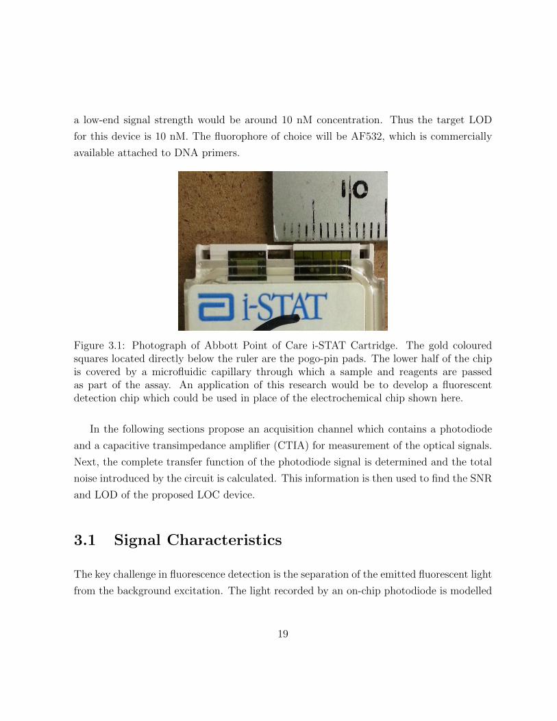
3.1 Photograph of Abbott Point of Care i-STAT Cartridge. The gold coloured
squares located directly below the ruler are the pogo-pin pads. The lower
half of the chip is covered by a microfluidic capillary through which a sample
and reagents are passed as part of the assay. An application of this research
would be to develop a fluorescent detection chip which could be used in
place of the electrochemical chip shown here. . . . . . . . . . . . . . . . . . 19
3.2 The implemented circuit and timing diagram for the signal acquisition chan-
nel. The switches are closed when the gate signal is high. . . . . . . . . . . 22
3.3 Photodiode equivalent circuit. . . . . . . . . . . . . . . . . . . . . . . . . . 23
3.4 S/H circuit using a 6T transmission gate and capacitor. . . . . . . . . . . . 25
xiii

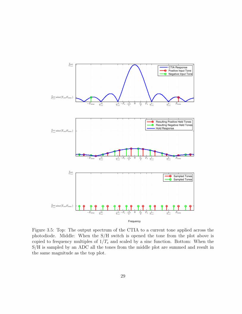
3.5 Top: The output spectrum of the CTIA to a current tone applied across the
photodiode. Middle: When the S/H switch is opened the tone from the plot
above is copied to frequency multiples of 1/Ts and scaled by a sinc function.
Bottom: When the S/H is sampled by an ADC all the tones from the middle
plot are summed and result in the same magnitude as the top plot. . . . . 29
3.6 Transimpedance magnitude of the CTIA (Eq. 3.7). Both the x and y axes
are plotted on a logarithmic scale. . . . . . . . . . . . . . . . . . . . . . . . 31
3.7 Three different styles of transmission gates used in a S/H. . . . . . . . . . 33
3.8 (a) Noise sources in the acquisition channel during the integration phase (b)
Noise sources in the acquisition channel during the reset phase . . . . . . . 36
3.9 The output magnitude for different input frequency sinusoidal current sig-
nals of 1A amplitude. . . . . . . . . . . . . . . . . . . . . . . . . . . . . . . 45
3.10 The output referred noise PSDs for the baseline shot noise, photodiode ther-
mal noise and dark current shot noise during the integration phase, in com-
parison to the total noise PSD of the acquisition channel. . . . . . . . . . . 46
3.11 The output referred noise PSDs for the baseline shot noise, photodiode ther-
mal noise and dark current shot noise during the reset phase, in comparison
to the total noise PSD of the acquisition channel. . . . . . . . . . . . . . . 47
3.12 The output referred noise PSDs for the output buffer and CTIA op-amp
during the integration phase and the reset phase of operation. It can be seen
that these three noise PSDs contribute are dominant for low frequencies and
high frequencies as their shape conforms closely to that of the total noise
PSD. . . . . . . . . . . . . . . . . . . . . . . . . . . . . . . . . . . . . . . . 48
3.13 The output referred noise PSDs for the reset and S/H switches. Both these
noise sources do not contribute significantly to the total output noise PSD
profile. . . . . . . . . . . . . . . . . . . . . . . . . . . . . . . . . . . . . . . 50
3.14 Sweeps of individual variables and the effect on the LOD . . . . . . . . . . 54
xiv
4.1 Acquisition channel transient voltage profiles. A DC current of 100nA was
applied to the anode of the diode to model the photocurrent. . . . . . . . . 56
4.2 Comparison between simulation results and values predicted by Eq. 3.7. . 57
4.3 Comparison between calculated and simulated S/H output magnitudes and
frequencies as a function of the photodiode current input frequency. . . . . 58
4.4 Comparison of the sampled simplified circuit simulation results to the tran-
sistor level and extracted simulations. A 50nA, 113Hz sine-wave with a 50nA
DC offset current was injected onto the photodiode for all three simulations.
An integration time of 250µs was used with a total period of 500µs . . . . 60
4.5 (a) Transient charge injection on VS/H for Vint = 1.95V . (b) Total charge
injection onto output of S/H circuit in isolation, as a function of input voltage. 62
4.6 Comparison between hand calculated and simulated transimpedance values
for the photodiode current while the CTIA is in reset. . . . . . . . . . . . . 63
4.7 Comparison of integrator output for different current input frequencies, with
and without accounting for the reset interference. It can be seen that the
reset interference does contribute to the output, however the derived model
does not completely explain the higher frequency effects taking place. . . . 64
4.8 The amplitude of various input tones (Red dots) correspond to the amplitude
of that predicted by the transfer function. . . . . . . . . . . . . . . . . . . 66
4.9 The amplitude of various input tones (Red dots) correspond to the ampli-
tude of that predicted by the transfer function. The spectra for the highest
frequency simulated tone was not able to be plotted due to simulator re-
lated issues, however the magnitude of the sinusoid was measured from the
transient Vout signal by hand. . . . . . . . . . . . . . . . . . . . . . . . . . 67
4.10 Comparison between predicted and simulated noise transfer function for S/H
transmission gate. This plot assumes a 100nA input sine-wave current. . . 69
4.11 Comparison between simulated and calculated output noise PSD of FCC
output buffer in unity feedback. . . . . . . . . . . . . . . . . . . . . . . . . 70
xv
4.12 The standard deviation of the sampled output as a function of the number
of samples taken. It can be seen that 100 samples is sufficient to provide an
accurate value for the standard deviation. . . . . . . . . . . . . . . . . . . 73
4.13 (a) Comparison between the calculated and simulated output noise gener-
ated by the CTIA op-amp. (b) Comparison between the calculated and
simulated output noise generated by noise sources located across the photo-
diode. . . . . . . . . . . . . . . . . . . . . . . . . . . . . . . . . . . . . . . 74
5.1 Complete layout of acquisition channel. . . . . . . . . . . . . . . . . . . . . 77
5.2 Comparison between measured and the loaded simulation of the output
referred noise PSD of the FCC op-amp. The slope of the low frequency
gain is determined by the flicker noise where as the high frequency slope
is determined by the gain roll off of the op-amp. The plateau at the high
frequency of the measured results is from the noise floor of the measurement
which occurs at 10−13V 2/Hz. . . . . . . . . . . . . . . . . . . . . . . . . . 79
5.3 (a) The output of the integrator as a function of time at 10 different optical
powers on the photodiode. (b) The maximum integrator value for each
applied optical power. . . . . . . . . . . . . . . . . . . . . . . . . . . . . . 81
5.4 The maximum integrator value at Tint for values of Voff . . . . . . . . . . . 82
5.5 (a) The discrete circuit implementation of CTIA. (b) Timing diagram for
discrete CTIA. Switches φ1 and φ2 are open on logic high. . . . . . . . . . 83
5.6 (a) Measured output of the current integrator for different incident light
intensities. (b) Line - The measured magnitude of the output voltage during
the hold phase. Shaded area - The predicted output region when accounting
for capacitor and LED intensity tolerances. . . . . . . . . . . . . . . . . . . 84
5.7 (a) Measured output of the CTIA for increasing durations of the integration
phase. Voff was set to ground, Th = 200µs, TReset = 50µs (b) Measured
output of the CTIA for increasing offset voltages applied to the non-inverting
terminal of the CTIA op-amp. . . . . . . . . . . . . . . . . . . . . . . . . 85
xvi
5.8 Output voltage of the integrator as a function of different optical input
frequencies. . . . . . . . . . . . . . . . . . . . . . . . . . . . . . . . . . . . 87
5.9 The noise as a function of photodiode photo-current. The measured data
back calculates the photodiode current based on the value of Cint and Tint.
The values for Cint = 10pF and Cint = 6.8pF are plotted here. . . . . . . . 89
5.10 Comparison between the total noise predicted and the measured as a func-
tion of Tint. . . . . . . . . . . . . . . . . . . . . . . . . . . . . . . . . . . . 90
6.1 Comparison between the predicted LOD performance and that calculated
from the measured signal and noise parameters. . . . . . . . . . . . . . . . 94
A.1 FCC Op-amp schematic. . . . . . . . . . . . . . . . . . . . . . . . . . . . . 99
A.2 Folded Cascode half circuit . . . . . . . . . . . . . . . . . . . . . . . . . . . 100
A.3 As the DC operating points change depending on the common mode volt-
age applied, Rout and Gm will change accordingly. This simulation was
performed using the specified bias voltages. . . . . . . . . . . . . . . . . . . 102
A.4 Top: Gain and Phase of the folded cascode op-amp unloaded. Maximum
gain is 69.8 dBv. Bottom: Gain as calculated by multiplying extracted gm
and Rout values. Maximum gain is around 70.0 dBv. . . . . . . . . . . . . . 103
A.5 As the output load is increased the gain at a common mode input voltage
of 1.65V increases until it plateaus. In the hand calculated model (Eq. A.5)
the gain manages to plateau around 400MΩ however in the simulation the
plateau doesn’t occur until much higher load impedances around 10GΩ. . . 104
A.6 Comparison between noise calculated using Eq. A.17 (adjusted for unity
gain, loaded with a 2pF capacitor) and that produced by SpectreRF. . . . 106
A.7 Transistor noise model . . . . . . . . . . . . . . . . . . . . . . . . . . . . . 107
A.8 Calculated input-referred noise voltage PSD of FCC op-amp accounting for
both shot and flicker noise. . . . . . . . . . . . . . . . . . . . . . . . . . . . 110
xvii
B.1 Luminosity function . . . . . . . . . . . . . . . . . . . . . . . . . . . . . . 112
C.1 Common source amplifier circuit to verify hand calculations . . . . . . . . 118
E.1 SNR vs Quantized ADC values . . . . . . . . . . . . . . . . . . . . . . . . 127
E.2 SNR as a function of the quantization of the DAC output signals. . . . . . 129
E.3 Relationship between photodiode current and the LED drive current. . . . 131
E.4 Memory map of OR1 control register. . . . . . . . . . . . . . . . . . . . . . 132
E.5 Register map of OR1 Status register . . . . . . . . . . . . . . . . . . . . . 133
G.1 Small signal model of the integrator during the reset phase of operation. Ro
and Co represent that output impedance of the op-amp. RSW is the switch
impedance of the transmission gate. RPD and CPD models the impedance
of the photodiode. IPD is the signal input from the photodiode. . . . . . . 137
G.2 Small signal model of the integrator during the integration phase of opera-
tion. The parameters remain the same as in Figure G.1 with the addition
of CH which is the capacitor the integrator output is sampled onto. The
output buffer isn’t shown here. . . . . . . . . . . . . . . . . . . . . . . . . . 137
G.3 Plot of various approximations of (G.10) . . . . . . . . . . . . . . . . . . . 140
xviii
List of Symbols
LCEE Light Collection Efficiency of Excitation
LCEFl Light Collection Efficiency of Fluorescence
µTAS Micro Total Analysis System
APD Avalanche Photodiode
ASIC Application Specific Integrated Circuit
CTIA Capacitive Transimpedance Amplifier
FCC Folded Cascode
FD Fluorescence Detection
FIFO First In-First Out Buffer
FLIM Fluorescence Lifetime Imaging
FWHM Full Width Half Maximum
LCE Light Collection Efficiency
LIF Laser Induced Fluorescence
LOC Lab-on-a-Chip
xix

MSPS Mega-sample per second
NA Numerical Aperture
OD Optical Density
PCB Printed Circuit Board
PMT Photo-Multiplier Tube
POC Point-of-Care
PSD Power spectral density
S/H Sample-and-hold
SBR Signal to Baseline Ratio
SNR Signal-to-Noise Ratio
SPAD Single-Photon Avalanche Diode
TIA Transimpedance Amplifier or Resistive Transimpedance Amplifier
xx

Chapter 1
Introduction
The development and evaluation of biological assays has long been carried out using cen-
tralized testing facilities. The requirements for large-scale bench-top infrastructure, expert
operators and costly reagents has restricted assay analysis to large, well-funded laborato-
ries. In recent years, however, there has been a surge in the development of point-of-care
(POC) diagnostic devices for applications in medicine [1], forensics [2] and food safety [3].
In 1990, micro total analysis systems (µTAS ) emerged suggesting that when some
biological assays are miniaturized, they operate faster, require less reagent and become
more sensitive [4]. With the advances in microfabrication, spurred by Moore’s law, it was
conceivable to integrate an entire assay onto a “lab-on-a-chip” (LOC) device. These devices
address the challenges preventing the migration of biological assays from centralized testing
facilities to POC testing by reducing platform size, shortening the time required to carry
out an assay and removing the need for expert operators.
The most common signal-acquisition [1, 3, 5] in conventional biological assays are optical
and electrochemical detection. Although the latter has been successfully employed in a
number of commercial POC products [6, 7], it has found less commercial use in genetic
analysis or other low concentration immunoassays due to its limited sensitivity. However, of
the variety of optical methods available, fluorescence detection (FD) has been widely used
in large-scale automated platforms for genome sequencing and protein microarrays due to
1

its superior specificity and sensitivity compared to electrochemical detection techniques
[8, 9].
While many research groups have focussed on constructing FD-based POC devices, FD
has not yet reached the level of integration and cost suitable for commercial POC devices
[5]. Market research has suggested that for LOC devices to be successful in the current
marketplace, they need to reach a manufacturing cost of $5 per test [10]. Additionally,
these devices must be nearly fully integrated, abstracting away the complexity of the
assay to allow for easy training and repeatable use [11]. Conventional FD systems require
confocal optics, stabilized laser sources, photo-multiplier tubes (PMTs) and high-quality
optical filters. Not only are these components expensive [12], but they are too bulky
to fit in a hand-held or easily-portable device [13, 14]. Alternative approaches, such as
proximity-based detection have demonstrated improved integration by eliminating the need
for collection optics [15, 16, 17], these devices still require substantial support infrastructure
such as external light sources and discrete electronic control and signal-acquisition circuits.
Platform size and cost in FD-based POC systems can be reduced by integrating the op-
tical and electronic components. To reduce the impact that discrete electronic components
have on POC device size, some research groups have integrated these using application-
specific integrated circuit (ASIC) technology [18, 19, 20, 21]. Other investigators have
also demonstrated various ways of integrating light sources into silicon devices such as
light-emitting diodes (LEDs) [22, 23], organic LEDs (OLEDs) [24, 25] and lasers [26]. A
monolithic LED and complementary metal-oxide-semiconductor (CMOS) detection circuit
has also been demonstrated [27], however no experimental results were provided. The ab-
sence of an optical filter is suspected for this omission. Later publications by the same
group demonstrated optical detection using a two-chip solution, with the light-source chip
placed down on the detection chip with the sample and high-quality optical filter placed
in between [28]. A hypothetical hybrid ASIC/microfluidic LOC device for FD detection is
shown in Figure 1.1. By depositing photo-polymer microfluidics on the surface of an ASIC
chip a monolythic LOC device can be made. Running an analyte through a micro-channel
located in the microfluidics, the sample can be optically interrogated by the ASIC below.
2

While reductions in platform form factor and cost are necessary to ensure widespread
use of FD-based POC devices, these systems must also provide sufficient detection limit
to be used for personal diagnostics. A review by Dandin et al. examined various µTAS
FD devices and concluded that, despite many demonstrations of this technology, none has
achieved sufficient sensitivity for low-brightness samples [5]. The metric of sensitivity for
FD is the limit of detection (LOD) which is the concentration of fluorophore measurable
at a given minimum signal-to-noise ratio (SNR).
This thesis focuses on the design of integrated and discrete signal-acquisition circuits
for a FD-based LOC device that would be appropriate for the system shown in Figure
1.1. The noise performance of these circuits is analyzed and compared to simulated and
experimental results in order to better understand the factors affecting the LOD and how
this metric can be improved. Chapter 2 provides additional background on fluorescence,
detection hardware, and LOC devices. In Chapter 3, the necessary optical signal strengths
are derived and a signal-acquisition-channel architecture is proposed. Analysis of the circuit
functions and noise of this architecture help to establish a model for improving the LOD of
FD-based LOC devices. Simulations of the acquisition channel in Chapter 4 validate the
derived noise calculations and circuit functions. The proposed signal-acquisition channel
is implemented (i) as an integrated circuit using the Austria Microsystems (AMS) 350 nm
CMOS process and (ii) using discrete components. Experimental results demonstrating
the circuit operation and noise performance of these devices are presented in Chapter 5.
3
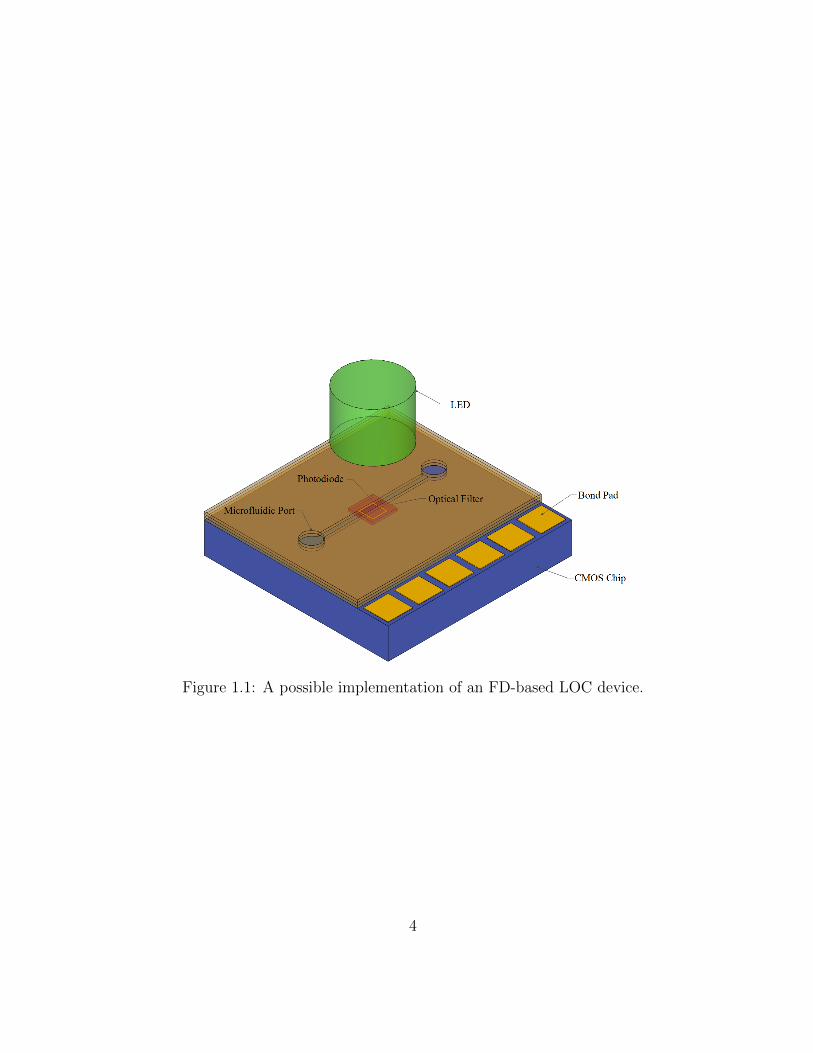
Figure 1.1: A possible implementation of an FD-based LOC device.
4
Chapter 2
Background
Constructing an FD-based LOC device while providing adequate detection limit poses
many engineering challenges. This chapter presents some of these challenges and lays out
a framework for the design decisions made later in this thesis.
Fluorescence detection requires three steps: excitation, emission and detection. Exci-
tation is the process of optically exciting the fluorescent molecule into a state. Emission
is the process by which the molecule returns to its resting state by re-emitting light at
a higher wavelength then the excitation light. Detection refers to the measurement of
fluorescent light using a photodetector and measurement circuitry.
The following sections provide a brief introduction to different fluorescent analytes
which can be used in biological assays. Additional background is given on matching flu-
orescent molecules to excitation sources. Various solutions to the challenge of separating
the excitation light from the emitted fluorescent light are then discussed. Following this,
some of the many optical detectors are examined. Only methods which can be practically
integrated into a monolithic device are examined.
5
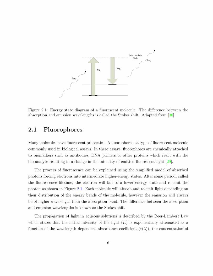
Intermediate State
hvi
hvs
hvihvs
Figure 2.1: Energy state diagram of a fluorescent molecule. The difference between theabsorption and emission wavelengths is called the Stokes shift. Adapted from [30]
2.1 Fluorophores
Many molecules have fluorescent properties. A fluorophore is a type of fluorescent molecule
commonly used in biological assays. In these assays, fluorophores are chemically attached
to biomarkers such as antibodies, DNA primers or other proteins which react with the
bio-analyte resulting in a change in the intensity of emitted fluorescent light [29].
The process of fluorescence can be explained using the simplified model of absorbed
photons forcing electrons into intermediate higher-energy states. After some period, called
the fluorescence lifetime, the electron will fall to a lower energy state and re-emit the
photon as shown in Figure 2.1. Each molecule will absorb and re-emit light depending on
their distribution of the energy bands of the molecule, however the emission will always
be of higher wavelength than the absorption band. The difference between the absorption
and emission wavelengths is known as the Stokes shift.
The propagation of light in aqueous solutions is described by the Beer-Lambert Law
which states that the initial intensity of the light (Io) is exponentially attenuated as a
function of the wavelength dependent absorbance coefficient (ε(λ)), the concentration of
6

the absorbent molecule (c) and the distance the light has propagated through the solution
(x), as described by Eq. 2.1:
ITx = Io · 10−ε(λ)·c·x (2.1)
The power density of light absorbed can then be described as IAb = Io − ITx however
examination of the typical values of the exponent allow for a Taylor approximation to be
performed reducing the absorption to a linear equation1:
IAb = Io · ln(10) · ε(λ) · c · x (2.2)
Not all photons that are absorbed are re-emitted as fluorescence. There is a scaling
factor called the quantum yield (φ) which determines the total emission intensity (IFl).
The quantum yield varies from fluorophore to fluorophore but is typically in the range of
0.2-0.7. This results in the total emission light intensity to be described by:
IEm = Io · φ · ln(10) · ε(λ) · c · x (2.3)
There are many higher order effects which influence fluorophore emission. Fluorescence
lifetime denotes the time constant of the decay from the higher intermediate state down
to the final resting state of the electron [32]. This has applications in fluorescence lifetime
imaging (FLIM) where to separate the excitation light from the fluorescence, the excitation
source is extinguished fast enough that the fluorescence is the only light present. Anisotropy
also can have an influence when dealing with polarized light sources and slow rotational
time-constants of the molecule [32]. When fluorophores are exposed to high-intensity light,
they can also undergo a process called photobleaching in which the fluorophores simply
stop re-emitting photons due to chemical changes.
1Factoring out Io, the equation becomes 1−10−A. A Taylor Expansion of 10−A = 1−A·ln(10)+1/2·A2 ·ln2(10)+... however as A = c·ε(λ)·x and a typical value of A = 10nM ·250000[1/(cm·M)]·30µm = 7.5·10−6,the coefficient of the third term A2 << A and the approximation becomes 1− 10−A = A · ln(10) [31].
7
2.2 Excitation Sources
A good pairing between the excitation light source and fluorophore is important for the
generation of a strong fluorescent signal. Additionally, as will be discussed in the next
section, the fluorescence emission spectrum should be as distinct from the excitation source
spectrum as possible. This means that ‘white’ sources such as metal-halide lamps, are not
generally appropriate.
The following subsections will provide an overview of different types of lasers, LEDs,
and OLEDs suitable as excitation sources. Some of the key physical parameters associated
with these devices include the spectral full width half maximum (FWHM), optical power
density and relative stability, as well as their scalability for monolithic integration.
2.2.1 Lasers
Lasers are the most commonly used excitation sources to induce fluorescence2. The coher-
ent light emitted from the laser results in a huge advantage in power density and small
FWHM (typically < 1 nm). This narrow spectrum makes it extremely easy to select optical
filters, which will be discussed more in Section 2.3.
While there are many types of lasers available, only semiconductor diode lasers are
appropriate for use as an integrated light source. Other types of lasers, such as diode,
pumped and dye, require a pressurized Fabry-Perot optical-resonating chamber or external
pumping laser to stimulate light emission [34].
Due to the well-established use of laser induced fluorescence (LIF), many fluorophores
have been optimized for use with the common laser-diode wavelengths (such as 405 nm, 532
nm, 635 nm and 670 nm [12]). The output power of diode lasers is typically on the order
of 5mW. Lasers can also be focused to the optical confinement limit of their particular
wavelength, allowing for maximum intensity.
2A simple search of Laser Induced Fluorescence in the Web of Knowledge Database yields approximately24,000 results [33]
8
The drawbacks associated with using diode lasers include optical stability and integra-
tion. Diode laser output is extremely temperature dependent and prone to jitter. Although
feedback stabilization can be used to improve stability to around 1%, low-frequency drift
(0.1 to 1 Hz) is still a common issue [35]. This presents a problem in biological assays
because fluorescent signal changes typically occur in the same signal bandwidth.
2.2.2 LEDs
The use of LEDs as excitation sources is becoming increasingly common [36]. LEDs demon-
strate several advantages over lasers such as lower cost, higher efficiency and better intensity
stability. There are disadvantages, however, mainly associated with the near isotropic light
emission pattern.
When a LED is forward biased, the current flow causes electrons and holes to recombine,
resulting in photon emission determined by the bandgap of the substrate. The variation
in energies of the electrons and holes result in variations in the wavelength of photons
emitted, giving LEDs a slightly larger FWHM (15 to 25 nm) than lasers. The large angle
of light emission from LEDs means that the power density of any fluorescent excitation
becomes geometry dependent. In integrated devices where the relative angles between
the analytes and the samples are large, this is less of a concern. However, it presents
a geometric challenge if any spacial filtering of the excitation light is to be employed.
Calculations provided in Appendix B.1 provide a power estimate of around 300µW for
geometries typical of microfluidic fluorescent detection.
Various groups have demonstrated the use of integrated LEDs for fluorescent detection.
Rae et al. showed LEDs deposited on an ASIC and used in conjunction with a single-photon
avalanche diode (SPAD) array to measure fluorescent dye [28]. Chediak et al. provided
a more compact implementation where a small LED was deposited on a PIN photodiode
below a microfluidic channel [37]. The most complete work to date has been the Ohta
group, which demonstrated a single ASIC beside a micro-LED on a polyimide substrate
[38].
9
2.2.3 OLEDs
Organic LEDs are a rapidly-developing technology and are very promising for use as in-
tegrated excitation sources. The basic physics of OLED light emission are very similar to
that of LEDs, however instead of using crystalline inorganic semiconductors such as GaAs
or GaN, they utilize organic compounds which exhibit similar properties. This presents sig-
nificant fabrication advantages in that instead of flip-chip bonding, as required for LEDs,
deposition processes compatible with conventional lithography can be used. Similar to
conventional LEDs, OLEDs have a broad spectral emission and emission angle.
There have been a number of demonstrations of OLEDs used as excitation sources for
fluorescence measurement devices. Pais et al. utilized an OLED and organic photodiode
to measure fluorescence detection in a thin film microfluidic device [39]. There have been
some very elaborate demonstrations of OLEDs on CMOS suggesting that this is a fairly
mature fabrication process. Levy et al. demonstrated a full 852x600 pixel three colour
OLED display on the surface of an ASIC [24]. Pais demonstrated output levels up to
1000cd/m2. Assuming a pixel size of 200x200 µm and a viewing angle of 90o, this provides
107 nW of optical power (Appendix B.1).
2.3 Fluorescent Separation
A key to increasing the sensitivity of circuits for FD is the use of optical methods to
eliminate the excitation light from the light measured by the detector. As Roulet et
al. explained, in a “typical” FD situation the fluorescent signal is 250,000 times weaker
than the baseline excitation light [40]. A measurement of the combined excitation and
fluorescent signal would require an 18-bit analog-to-digital converter (ADC), and only
a single bit would represent the signal. In order to improve this signal-to-baseline ratio
(SBR), optical methods for separating these two signals must be employed. Various options
will be explored in the following subsections.
There are three key features of the fluorescent light which can be exploited to separate
10
it from the excitation. Spectrally, there is a difference in wavelength between the excitation
and fluorescent light. Geometrically, the excitation light will come from the direction of its
source; the fluorescent light can be emitted in any direction. Finally, there is a temporal
difference between the excitation of the fluorophore and the re-emission of the fluorescence.
2.3.1 Spectral Separation
Exploiting the spectral differences between excitation and fluorescent light, it is possible to
select optical filters which will attenuate the former light while transmitting the latter. The
effectiveness of the transmittance of the filter is measured in either optical density (OD),
decibels or percent. This work will use optical density which is described mathematically
by Eq. 2.4 [40].
OD(λ) = −log10(ITx(λ)
Io(λ)
)(2.4)
As the excitation and the fluorescence will have distinct spectral profiles, both will have
a different effective transmission through the filter. This work will use the notation ODE
and ODFl for the effective optical densities of the excitation and fluorescent light, respec-
tively. The effective OD can be found by replacing the wavelength dependent intensities
in Eq. 2.4 with the total intensities. An ideal optical filter would provide a large ODE and
an ODFl of zero.
Absorbance filters utilize Beer-Lambert’s Law to selectively filter specific wavelengths
dependent on the chemical structure of the filter. The thickness of these filters will ulti-
mately determine the attenuation. A challenge with this type of filter is autofluorescence.
The chemical structure of these pigments may end up re-emitting the photons at higher
wavelengths to dissipate the energy absorbed. As the material is made thicker eventu-
ally the amount of re-emitted light will become greater than the increased absorbed light,
limiting the performance of the filter.
Interference filters are commonly used commercially available filters. These filters con-
tain multiple layers of different index materials which cause components of the light to
11
reflect and destructively interfere with the incoming light. By precisely depositing these
layers, sharp cut off frequencies can be achieved by such filters [5]. These filters also typi-
cally provide incredible high attenuation (ODE < 5). Groups such as Burns [41, 15] have
deposited such filters directly onto photodiodes for use with fluorescence detection.
The main disadvantage with interference filters is that they do not work very well if
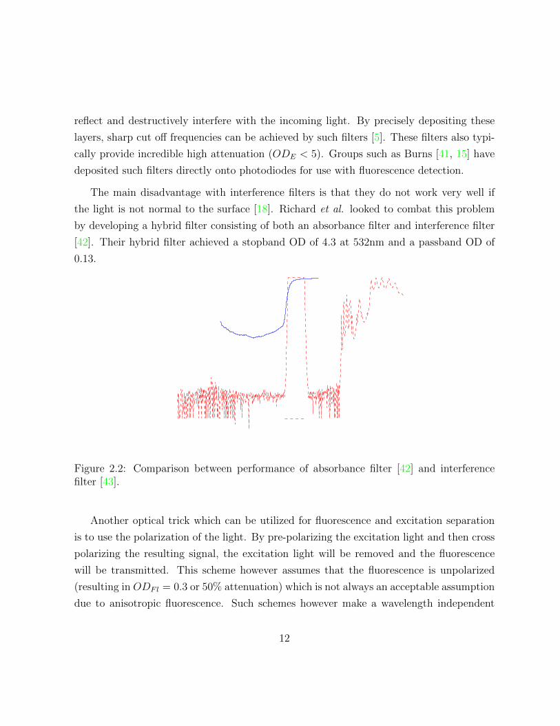
the light is not normal to the surface [18]. Richard et al. looked to combat this problem
by developing a hybrid filter consisting of both an absorbance filter and interference filter
[42]. Their hybrid filter achieved a stopband OD of 4.3 at 532nm and a passband OD of
0.13.
Figure 2.2: Comparison between performance of absorbance filter [42] and interferencefilter [43].
Another optical trick which can be utilized for fluorescence and excitation separation
is to use the polarization of the light. By pre-polarizing the excitation light and then cross
polarizing the resulting signal, the excitation light will be removed and the fluorescence
will be transmitted. This scheme however assumes that the fluorescence is unpolarized
(resulting in ODFl = 0.3 or 50% attenuation) which is not always an acceptable assumption
due to anisotropic fluorescence. Such schemes however make a wavelength independent
12
fluorescent filter, allowing for multiplexed fluorophores to be used without further design
consideration being given to the filter. These filters typically achieve ODE of 2.5 - 2.9
[39, 44]. Some groups have also explored hybrid polarizer-filter techniques and have seen
ODE as high as 8 at some wavelengths [45].
2.3.2 Geometric separation
To geometrically separate the fluorescent light from the excitation light is fairly easy when
using a laser excitation light source. As the laser only propagates along a single path and
the fluorescence emits isotropically, the detector can simply be placed out of the path of
the laser. As the devices scale however this becomes more difficult. Using isotropic light
sources such as LEDs or OLEDs, this becomes much more complicated.
With photo-lithography and laser ablation being the most common form of microfluidic
fabrication, the devices are usually constrained to being two dimensional. This has largely
limited the excitation sources to being either shining directly into the detector, orthogonal
to the detector or to illuminating from the same plane as the detector.
To abstract away much of the optical modelling required to accurately predict the
amount of fluorescence or excitation light collected, a coefficient is introduced: the Light
Collection Efficiency (LCE), which is defined as the total power incident normalized by
the total power input. In confocal optical systems the LCE is dictated by the Numerical
Aperture (NA) of the device optics [18]. In integrated devices, such as the one presented by
Burns et al. [41] where the detector is placed directly below the microfluidic channel, the
LCE of Fluorescence (LCEFl) is determined by the size of the detector and the distance
between the detector and the channel [5]. By modelling the fluorescences as an isotropic
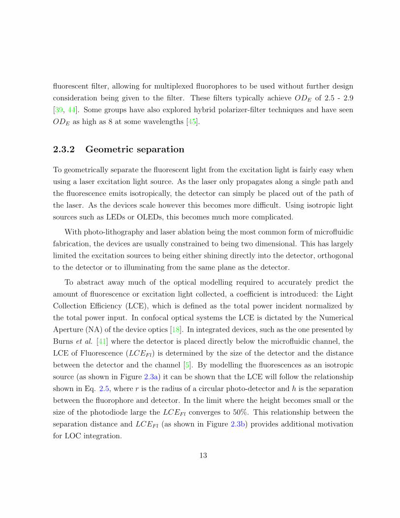
source (as shown in Figure 2.3a) it can be shown that the LCE will follow the relationship
shown in Eq. 2.5, where r is the radius of a circular photo-detector and h is the separation
between the fluorophore and detector. In the limit where the height becomes small or the
size of the photodiode large the LCEFl converges to 50%. This relationship between the
separation distance and LCEFl (as shown in Figure 2.3b) provides additional motivation
for LOC integration.
13

LCEFl =1
2
(1− h√
h2 + r2
)(2.5)
(a)
10−7
10−6
10−5
10−4
10−3
10−2
10−1
0
5
10
15
20
25
30
35
40
45
50
Separation between photodiode and microfluidic channel [m]
LC
EF
l [%
]
(b)
Figure 2.3: (a) Diagram of fluorescent point source light collection by photodiode. (b) Plotof LCEFl as a function of the dimension h for a photodiode with a 100µm radius.
This provides additional motivation for integrating fluorescence detection on-chip. In
order to maximize LCEFl the separation must be minimized, which means that the ideal
situation is to have the microfluidic deposited directly onto the surface of the photodiode.
This however imposes a trade off between LCEFl and Excitation Light Collection Efficiency
(LCEE).
The LCEE has a significant influence on the strength of the excitation background
signal. In discrete FD devices, it is possible to implement fluidic configurations which limit
the LCEE to less than 1%. When FD is scaled an integrated, it comes increasingly difficult
to illuminate the microfluidic channel without increasing LCEE to near unity.
Some groups have elected to ignore this trade off and simply maximize the LCEFl
and collect nearly all the excitation light (LCEE ≈ 1) [17, 45, 46, 47]. Others illuminate
the microfluidics orthogonal to the detector, reducing the LCEE to 0.3-5% [13, 16, 18,
14
48, 49, 50] with either the use of waveguides or using focused excitation. Chediak et al.
demonstrated an excitation source built into the same GaAs substrate as the detector [37].
An other group demonstrated a wave-guide etched into the substrate which then reflected
the light up into the channel from below and collected the fluorescence through a similar
structure [51]. Other groups have employed wavelength dependent diffraction to send the
excitation a different direction from the fluorescence [52, 53].
2.3.3 Temporal
The delay between the excitation of the fluorophore and the re-emission of the photon is a
decay with a time constant on the order of nanoseconds. With suitably fast electronics it
is possible to shutter the light source and record the decay of the fluorescence [28, 54, 55].
This form of detection could soften the requirement of other forms of optical separation,
however this increases the complexity and speed required by the photo-detector and light
source.
2.4 Photodiodes
A photodetector is required to convert emitted photons to electrons which can be measured
by a signal-acqusition circuit. The most common form of on-chip photodetectors are pho-
todiodes. Photodiodes are simple, well-characterized devices with good optical properties
and can be implemented in almost any CMOS process.
Silicon photodiodes are formed from a p-n junction and are normally operated under
reverse-bias conditions. When a photon is absorbed in the depletion region, an electron-
hole pair is created. Due to the applied electric field, the electron is swept to the cathode
and the hole is swept to the anode. This charge separation results in a capacitance across
the photodiode along with a light-dependent current. A greater light intensity on the
photodiode results in a larger current flow. There is a large shunt resistance across the
diode which results in a leakage path across the diode. Photodiodes exhibit limited gain
15
as a single photon can only produce, at most, a single electron-hole pair. As a result, for
low light intensities, noise can dominate over the photocurrent.
The photocurrent produced by the photodiode IPD is given by:
IPD = e−η
(P · λh · c
)(2.6)
where e− is the charge of an electron, η is the quantum efficiency of the photodiode,
P is the power incident on the photodiode, λ is the wavelength of light, h is Planck’s
constant, and c is the speed of light [34]. It is common to reduce these terms to a linear
scaling factor called the responsivity (Resp) measured in units of A/W. The conversion
from incident power to output current can be described by:
IPD = Resp · P (2.7)
2.5 Measurement Electronics
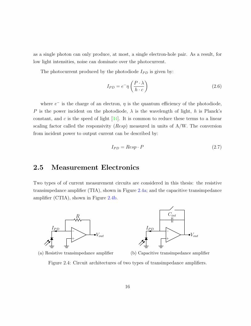
Two types of of current measurement circuits are considered in this thesis: the resistive
transimpedance amplifier (TIA), shown in Figure 2.4a; and the capacitive transimpedance
amplifier (CTIA), shown in Figure 2.4b.
IPD −
+Vout
R
(a) Resistive transimpedance amplifier
IPD −
+Vout
Cint
(b) Capacitive transimpedance amplifier
Figure 2.4: Circuit architectures of two types of transimpedance amplifiers.
16
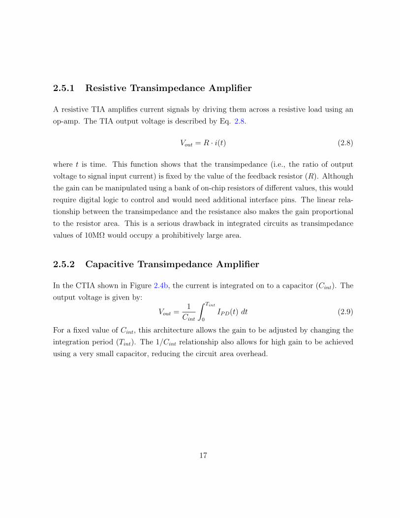
2.5.1 Resistive Transimpedance Amplifier
A resistive TIA amplifies current signals by driving them across a resistive load using an
op-amp. The TIA output voltage is described by Eq. 2.8.
Vout = R · i(t) (2.8)
where t is time. This function shows that the transimpedance (i.e., the ratio of output
voltage to signal input current) is fixed by the value of the feedback resistor (R). Although
the gain can be manipulated using a bank of on-chip resistors of different values, this would
require digital logic to control and would need additional interface pins. The linear rela-
tionship between the transimpedance and the resistance also makes the gain proportional
to the resistor area. This is a serious drawback in integrated circuits as transimpedance
values of 10MΩ would occupy a prohibitively large area.
2.5.2 Capacitive Transimpedance Amplifier
In the CTIA shown in Figure 2.4b, the current is integrated on to a capacitor (Cint). The
output voltage is given by:
Vout =1
Cint
∫ Tint
0
IPD(t) dt (2.9)
For a fixed value of Cint, this architecture allows the gain to be adjusted by changing the
integration period (Tint). The 1/Cint relationship also allows for high gain to be achieved
using a very small capacitor, reducing the circuit area overhead.
17
Chapter 3
Design
This chapter presents the analysis and design of a signal acquisition channel for the ASIC
CMOS of a LOC FD chip, such as the one shown in Figure 1.1. The design requirements
are for a transimpedance amplifier integrated with a single on-chip photodiode. This
channel must have adequate sensitivity/limit of detection (LOD) to be used for fluorescence
detection, as well as a small chip area and minimal pin count.
A low pin count is important as interfacing with CMOS with microfluidic post-processing
provides a significant design challenge. For example Abbott Point of Care’s i-STAT car-
tridge system utilizes pogo-pins to create electrical contact, each pin requiring roughly
1mm2. In a full CMOS process this would be prohibitively expensive and thus a minimal
pin-count should be maintained.
Of the variety of FD based biological assays, this work will focus on its application for
genetic analysis. Genetic analysis assays make extensive use of fluorophore labels. Using
labelled DNA sequences, called primers, to bind to a DNA sample, information can be
gained about the order and length of the target. Polymerase chain reaction (PCR) is the
standard way to genetically amplify DNA samples, where each amplified copy becomes
tagged with a fluorophore. In a typical PCR reactions, a starting concentration of fluores-
cently labelled primers is around 100 nM and the relative PCR yield (conversion of primers
to product) is usually between 5-50% depending on how optimized the reaction is. Thus
18
a low-end signal strength would be around 10 nM concentration. Thus the target LOD
for this device is 10 nM. The fluorophore of choice will be AF532, which is commercially
available attached to DNA primers.
Figure 3.1: Photograph of Abbott Point of Care i-STAT Cartridge. The gold colouredsquares located directly below the ruler are the pogo-pin pads. The lower half of the chipis covered by a microfluidic capillary through which a sample and reagents are passedas part of the assay. An application of this research would be to develop a fluorescentdetection chip which could be used in place of the electrochemical chip shown here.
In the following sections propose an acquisition channel which contains a photodiode
and a capacitive transimpedance amplifier (CTIA) for measurement of the optical signals.
Next, the complete transfer function of the photodiode signal is determined and the total
noise introduced by the circuit is calculated. This information is then used to find the SNR
and LOD of the proposed LOC device.
3.1 Signal Characteristics
The key challenge in fluorescence detection is the separation of the emitted fluorescent light
from the background excitation. The light recorded by an on-chip photodiode is modelled
19
as having two separate components: background excitation light PB and fluorescent emis-
sion light PFl, both measured in watts. Based on the review by Dandin [5], these can be
described analytically as:
PB = ILED · APD · LCEB · 10−ODB (3.1)
PFl = ILED · ACh · LCEFl · 10−ODFl · ln(10) · ε · c · d · φ (3.2)
where APD is the photodiode area; ACh is the illuminated area of the microfluidic channel
containing the fluorescent molecules; ILED is the intensity of the LED; LCEE and LCEFl
are the light collection efficiency of the photodiode for the background and fluorescence
light respectively (a geometric parameter); OD is the attenuation due to optical filters; c
is the concentration of the fluorophore; d is the optical path length of the channel; ε is the
extinction coefficient of the fluorophore; and φ is the quantum yield of the fluorophore.
Table 3.1 provides a set of model parameters which can be expected for a LED top-
illuminated FD system as shown in Figure 1.1. Equations 3.2 and 3.1 predict the back-
ground and fluorescent optical signal power to be 400 nW and 10.5 pW respectively. This
illustrates the challenge of measuring a signal that is four orders of magnitude smaller than
the baseline.
The conversion from optical power to electric current is described by Eq. 2.7. A typical
value of responsivity is around 0.29 A/W for optical wavelengths around 500 nm. This gives
an electrical current of 3.06 pA for the fluorescent signal and 116nA for the background
current.
The frequency content of the fluorescent signal in conventional FD applications, is
typically fairly low. For example, the fluorescent signal in Capillary Electrophoresis, is a
function of the change in concentration (c in Eq. 3.2) which fluctuates at a rate of 10-50Hz.
These slowly changing fluctuations mean that circuit speed is not critical. The background
excitation signal is DC.
20
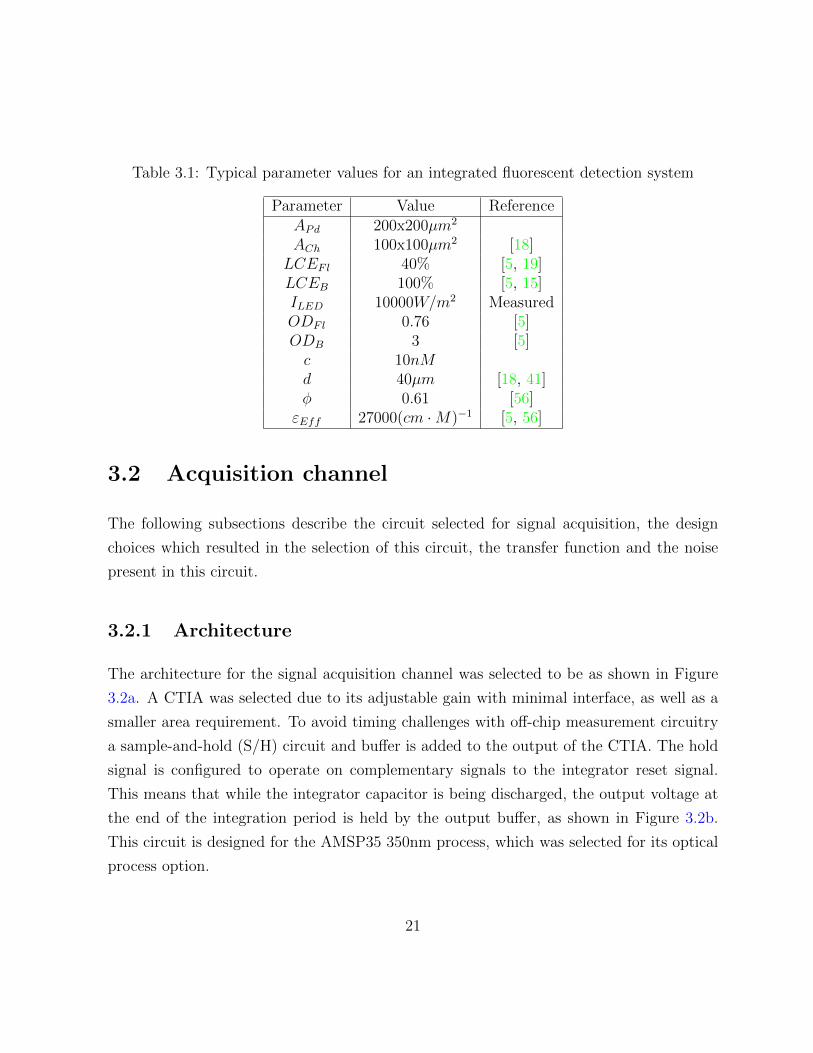
Table 3.1: Typical parameter values for an integrated fluorescent detection system
Parameter Value ReferenceAPd 200x200µm2
ACh 100x100µm2 [18]LCEFl 40% [5, 19]LCEB 100% [5, 15]ILED 10000W/m2 MeasuredODFl 0.76 [5]ODB 3 [5]c 10nMd 40µm [18, 41]φ 0.61 [56]
εEff 27000(cm ·M)−1 [5, 56]
3.2 Acquisition channel
The following subsections describe the circuit selected for signal acquisition, the design
choices which resulted in the selection of this circuit, the transfer function and the noise
present in this circuit.
3.2.1 Architecture
The architecture for the signal acquisition channel was selected to be as shown in Figure
3.2a. A CTIA was selected due to its adjustable gain with minimal interface, as well as a
smaller area requirement. To avoid timing challenges with off-chip measurement circuitry
a sample-and-hold (S/H) circuit and buffer is added to the output of the CTIA. The hold
signal is configured to operate on complementary signals to the integrator reset signal.
This means that while the integrator capacitor is being discharged, the output voltage at
the end of the integration period is held by the output buffer, as shown in Figure 3.2b.
This circuit is designed for the AMSP35 350nm process, which was selected for its optical
process option.
21

IPD
VPD −
+ VintVoff
φ VS/H
CH
−
+Vout
Cint
φ
(a) Acquisition channel circuit
φ
Mode: Hold/Reset Integrate Hold/Reset Integrate
Vint
VS/HVout
t = to t = to + Tint t = to + Ts t = to + Tint + Ts
Tint Th
Ts
(b) Timing diagram
Figure 3.2: The implemented circuit and timing diagram for the signal acquisition channel.The switches are closed when the gate signal is high.
3.2.2 Channel Components
Provided in the following sections is an explanation and justification for the selection of
this acquisition channel circuit architecture, along with a derivation of their respective
transfer functions.
Photodiode
The main consideration with regards to the photodiode is the area sizing. The sizing
is heavily dependent on the geometry of fluorescent sample to be measured. In the tar-
22

geted microfluidic applications such as CE, the channel width is typically around 100 µm
[48]. With the targeted implementation of the microfluidics being a post-processed photo-
polymer, the separation between the photodiode and the channel is expected to be on the
order of 20-50 µm [57].
The geometric parameter which determines the sizing of the photodiode is the light
collection efficiency (LCEFl) (shown in Eq. 2.5). As the limit of this equation provides a
maximum value of 50%, a diameter of the photodiode should be selected to give a value
close to this. By selecting an edge length of 200µm, the LCEFl is close to its maximum
without occupying excessive area.
Although the AMSP35 process kit comes with a photodiode standard cell, its dimen-
sions are limited to a maximum of 150µm. This photodiode is a p-sub/n-well structure
with a guard ring on all sides. As the standard cell does not provide layouts of sufficient
size, a scaled version of this cell was laid out by hand.
The photodiode responsivity is specified to be 0.29 A/W (at a wavelength of 500nm) in
the AMSP35 process [58]. This wavelength provides a sufficiently accurate approximation
of the responsivity for all optical signals considered in this thesis.
The photodiode is electrically modelled as shown in Figure 3.3. The sizing of the photo-
diode influences its effective capacitance and resistance. The small size of the photodiode
and large number of substrate contacts allows Rs to be neglected. The AMSP35 process
is specified to have a diode area capacitance of 0.08fF/µm2. Typical values of RPD for
discrete photodiodes are extremely large (100MΩ to 10GΩ [12]). With the small junction
area of the on-chip photodiode, the resistance will be even larger, making the photodiode
effectively a current source in parallel with a capacitor.
AnodeRs
RPDCPDIPD
Cathode
Figure 3.3: Photodiode equivalent circuit.
23

Capacitive Transimpedance Amplifier
The CTIA is made up of three components: an op-amp, feedback capacitor and switch.
For the op-amp a folded cascode NMOS input architecture is used. The full analysis of this
op-amp is provided in Appendix A. The op-amp open-loop transfer function is modelled
as a single pole response described by:
A(f) =Ao
1 + j·ff3dB
(3.3)
where Ao is the open loop gain (Rout ·Gm) and f3dB is the corner frequency of the op-amp.
The feedback switch is implemented using a NMOS and PMOS pass transistor with dummy
transistors for charge injection reduction. A more complete analysis of this is provided in
the Sample and Hold Section.
The periodic reset of the CTIA is necessary to prevent saturation of the op-amp. This
results in a sinc-response profile of the transimpedance function. The complete response
of the CTIA in Figure 3.2a is described by Eq. 3.4 which is derived in Appendix D.
Vint(f)
IPD(f)=
Tint
Cint + CPD+Cint
A(f)
· sinc (f · Tint) (3.4)
The op-amp response results in a single pole located at:
f ≈ Cint · Ao · f3dB(CPD + Cint)
(3.5)
Noting however, that the sinc(f · Tint) has an effective 3dB frequency located at f =
0.44/Tint it can safely be assumed that:
0.44
Tint Cint · Ao · f3dB
(CPD + Cint)(3.6)
24

allowing for Eq. 3.4 to be reduced to:
Vint(f)
IPD(f)=TintCint· sinc (f · Tint) (3.7)
Sample and Hold
Although there are many varieties of S/H circuits available in the literature, an architecture
consisting of a transmission gate and hold capacitor is used in this work. A challenge with
this style of S/H is charge injection which results from the charge being ejected from
the transmission gate channel when the switch is opened. Various charge cancellation
techniques can be used to mitigate this non-ideality. This work will make use of the
architecture shown in Figure 3.4 because it minimizes the impact of charge injection and
its ability to pass voltages close to ground and VDD without losing a threshold drop. The
effects of charge injection will be explored further in Section 3.2.4.
Vin
Wn
Wp
Vout
CH
Wp
2
Wn
2
Wp
2
Wn
2
φ
φ
Figure 3.4: S/H circuit using a 6T transmission gate and capacitor.
When the transmission gate is closed, the applied voltage (Vin) is transferred to the hold
capacitor Ch. When the switch is opened the voltage present on the capacitor is effectively
sampled. In the context of the signal path described in Figure 3.2a, the time-domain
representation of the sampled-and-held signal is [59]:
VS/H(t) =
(V ′S/H(t) ·
∞∑k=−∞
δ(t− (t0 + k · Ts + Tint))
)∗ rect
(t
Th
)(3.8)
where V ′S/H(t) is the time domain output signal when the switch is closed and rect(t/T ) =
25
u(t+ T/2)− u(t− T/2), where u(t) is the Heaviside step function. Times t0, Ts, Tint, and
Th are all described by the timing diagram given in Figure 3.2b. It is possible to describe
VS/H(t) in the frequency domain by noting that convolution by a rect function becomes
a multiplication by a sinc and that multiplication by a Dirac delta function becomes a
convolution by a delta function. To simplify variables, fk = f − k/Ts. The frequency-
domain response at the S/H output is given by:
VS/H(f) = V ′S/H(f) ∗∞∑
k=−∞
δ(fk) ·ThTs· sinc(f · Th) · e−j2πf ·(t0+Tint) (3.9)
=ThTs· sinc(f · Th) · e−j2πf ·(t0+Tint) ·
∞∑k=−∞
V ′S/H(fk) (3.10)
whereV ′S/H(f) is Vint(f) after it is passed through the RC filter of S/H. This is given by:
V ′S/H(f) =Vint(f)
1 + j2π f RSW CH(3.11)
where RSW is the on resistance of the transmission gate.
Output Buffer
The purpose of the output buffer is to drive the voltage from across the hold capacitor
off-chip without drawing charge from this capacitor. A basic unity feedback op-amp con-
figuration is therefore implemented, using the same FCC op-amp as for the CTIA. The
differential open-loop response of the op-amp is described by Eq. 3.3. Using the voltage
definitions described in Figure 3.2a, the unity feedback configuration forces the output to
be:
Vout(s) = A(s) · (VS/H(s)− Vout(s)) (3.12)
resulting in the transfer function:
Vout(s)
VS/H(s)=
A(s)
A(s) + 1(3.13)
26
Sampling of Acquisition Channel Output
Implicit in the derivation of the CTIA frequency response is that the output of the amplifier
is sampled during the hold mode of operation. This will transform the signal from a
continuous time equation into a discrete time equation as described by:
Vout(t) = V ′out(t) ·∞∑
n=−∞
δ(t− n Ts) (3.14)
where V ′out(t) is the output of the buffer prior to sampling. This aliases the frequency
spectrum coming out of the output buffer and limits the measurable spectrum to less than
1/(2 Ts).
To allow for a more intuitive explanation the circuit will first be simplified by assuming
that the pole resulting from the S/H is high frequency and output buffer does not contribute
to the frequency response. Consider a current input tone of frequency Ftone and unit
magnitude applied to the input of the CTIA. The magnitude of the output of the CTIA
will be described by:
Vint(f) =TintCint
sinc(TintFtone) · δ(f − Ftone) (3.15)
as shown in the top of Figure 3.5. When the switch of the sample and hold is opened the
tone will be copied around the spectrum and scaled by a sinc function and the duty cycle
of the hold period as given by:
VS/H(f) =ThTssinc(Thf)
∞∑k=−∞
TintCint
sinc(TintFtone) · δ(f − Ftone −k
Ts) (3.16)
as shown in the middle of Figure 3.5. When the S/H output is sampled by an ADC the
spectrum is folded down into the baseband and all the copied tones from the middle plot
27
of Figure 3.5 are summed. Using the identity [60]:
∞∑n=−∞
sin((n− a)θ)
n− a = π (3.17)
where 0 < θ < 2π and a is unbounded, it can be shown that the sum of these tones will
equal the magnitude of the output of the CTIA as shown by:
TintCint
sinc(TintFtone) =TintCint
sinc(TintFtone)ThTs
∞∑n=−∞
sinc(Th(Ftone −n
Ts)) (3.18)
The location of the tone in the measured output is determined by the relationship:
fout = Ftone −p
Ts(3.19)
where p is an integer which force fout to lie between 0 and Fs/2. As a result of the aliasing
fout does not map one-to-one with Ftone. Multiple values of Ftone can be placed at the
same frequency of fout. Thus, when superposition is applied and Ftone is allowed to be a
continuum of frequencies, the sum of all values of p must be taken. This results in the
output spectrum of the sampled results being described by:
Vout(f) =∞∑
p=−∞
TintCint
sinc(Tint(f −p
Ts)) · IPD(f − p
Ts) (3.20)
The infinite summation and limitations on the output frequency values for which Vout(f)
can be evaluated, makes it difficult to attain intuitive understanding of the mathematical
relationships of aliased functions. As a result, it will be more helpful in coming sections to
plot the output magnitude as a function of the input frequency.
Removing the assumptions of a high gain of the output buffer and high pole frequency
28
−Ftone−2Tint
−1Tint
−Fs−Fs
20 Fs
2Fs
1Tint
2Tint
Ftone
Tint
Cintsinc(TintFtone )
Tint
Cint
−Ftone−2Tint
−1Tint
−Fs −Fs
20 Fs
2Fs
1Tint
2Tint
Ftone
Tint
Cintsinc(TintFtone )
Frequency
−Ftone−2Tint
−1Tint
−Fs −Fs
20 Fs
2Fs
1Tint
2Tint
Ftone
Tint
Cintsinc(TintFtone )
Tint
Cint
CTIA Response
Positive Input Tone
Negative Input Tone
Resulting Positive Held Tones
Resulting Negative Held Tones
Hold Response
Sampled Tones
Sampled Tones
Figure 3.5: Top: The output spectrum of the CTIA to a current tone applied across thephotodiode. Middle: When the S/H switch is opened the tone from the plot above iscopied to frequency multiples of 1/Ts and scaled by a sinc function. Bottom: When theS/H is sampled by an ADC all the tones from the middle plot are summed and result inthe same magnitude as the top plot.
29
of the S/H, the output spectrum is described by:
Vout(f) =∞∑
p=−∞
Vint(f − pTs
)
1 + j2π(f − pTs
) ·RSWCH
A(f − nTs
)
A(f − nTs
) + 1(3.21)
provided sinc(Av · f3dB · Th) ≈ 0.
3.2.3 Voltage Magnitude Spectrum of Complete Signal Acquisi-
tion Channel
The complete voltage magnitude spectrum describing the signal acquisition channel is
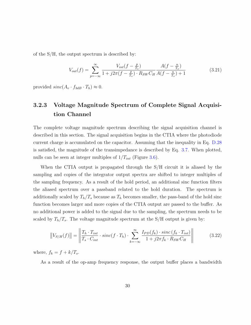
described in this section. The signal acquisition begins in the CTIA where the photodiode
current charge is accumulated on the capacitor. Assuming that the inequality in Eq. D.28
is satisfied, the magnitude of the transimpedance is described by Eq. 3.7. When plotted,
nulls can be seen at integer multiples of 1/Tint (Figure 3.6).
When the CTIA output is propagated through the S/H circuit it is aliased by the
sampling and copies of the integrator output spectra are shifted to integer multiples of
the sampling frequency. As a result of the hold period, an additional sinc function filters
the aliased spectrum over a passband related to the hold duration. The spectrum is
additionally scaled by Th/Ts because as Th becomes smaller, the pass-band of the hold sinc
function becomes larger and more copies of the CTIA output are passed to the buffer. As
no additional power is added to the signal due to the sampling, the spectrum needs to be
scaled by Th/Ts. The voltage magnitude spectrum at the S/H output is given by:
∥∥VS/H(f)∥∥ =
∥∥∥∥∥Th · TintTs · Cint· sinc(f · Th) ·
∞∑k=−∞
IPD(fk) · sinc (fk · Tint)1 + j2πfk ·RSWCH
∥∥∥∥∥ (3.22)
where, fk = f + k/Ts.
As a result of the op-amp frequency response, the output buffer places a bandwidth
30
Frequency [Hz]
Tra
nsim
pedance [lo
g 10(V
/A)]
1Tint
10Tint
100Tint
Tint
Cint
Figure 3.6: Transimpedance magnitude of the CTIA (Eq. 3.7). Both the x and y axes areplotted on a logarithmic scale.
limit on the signal output resulting in a output voltage magnitude of:
‖Vout(f)‖ =
∥∥∥∥∥Th · TintTs · Cint· sinc(f · Th) ·
∞∑k=−∞
IPD(fk) · sinc (fk · Tint)1 + j2πfk ·RSWCH
· Ao · f3dBf3dB · (Ao + 1) + j · f
∥∥∥∥∥(3.23)
As a result of frequency aliasing from the ADC, the spectrum is folded over when
sampled. This results in a measured frequency domain spectrum of:
Vout(f) =TintCint
∞∑p=−∞
sinc(
(f − pTs
) · Tint)· IPD(f − p
Ts)
1 + j2π(f − pTs
) ·RSWCH·
A(f − pTs
)
A(f − pTs
) + 1(3.24)
31
3.2.4 Acquisition Channel Interference
Non-idealities in the operation of the acquisition channel result in systematic addition
of unwanted signals. Different from noise, these interfering signals are not generated by
random processes and could, in principle, be determined and removed. The two sources
of interference that are discussed in the following sections are: charge injection by the
transmission gates and interference generated by the photodiode while the integrating
capacitor is being reset.
Switch Charge injection
The chief problem with simple transmission gates is charge injection. When the gate is
closed, charge is forced out of the MOSFET channel and injected onto the trace on either
side of the FET [61]. Should a capacitor be located at one or both ends of the transmission
gate, the injected charge will affect the voltage on the capacitor. In the case of the S/H
circuit shown in Figure 3.7a, the charge injected by a single NMOS results in a change of
voltage described by:
∆V =Wn · Ln · Cox(Vφ − Vin − VTH)
2CH(3.25)
where Wn and Ln are the dimensions of the transistor, Cox is the gate oxide capacitance
per unit area, Vφ is the gate voltage, Vin is the voltage being passed by the gate, VTH is
the transistor threshold voltage and CH is the hold capacitor value of the S/H.
One technique for reducing charge injection is to use parallel PMOS and NMOS tran-
sistors as the switch as shown in Figure 3.7b. When the gate is switched off, the PMOS will
eject holes and the NMOS will eject electrons which will ideally cancel the total injected
charge. This configuration provides the additional advantage of passing both a hard 0 and
a hard VDD. One issue with this is that the charge injected by the PMOS and NMOS do
not cancel completely because the charge from each is a function of Vin. However, if the
transistors are sized such that a midrange value of Vin provides no charge injection, this
non-ideality can be minimized. By first setting the charge ejected from each transistor
32
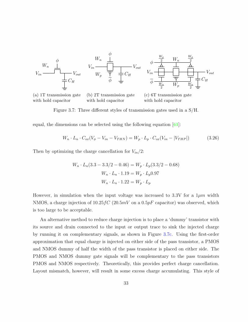
Vin
Wn
φ
CH
Vout
(a) 1T transmission gatewith hold capacitor
Vin
Wn
φ
CHφ
Wp
Vout
(b) 2T transmission gatewith hold capacitor
Vin
Wn
Wp
Vout
CH
Wp
2
Wn
2
Wp
2
Wn
2
φ
φ
(c) 6T transmission gatewith hold capacitor
Figure 3.7: Three different styles of transmission gates used in a S/H.
equal, the dimensions can be selected using the following equation [61]:
Wn · Ln · Cox(Vφ − Vin − VTHN) = Wp · Lp · Cox(Vin − |VTHP |) (3.26)
Then by optimizing the charge cancellation for Vin/2:
Wn · Ln(3.3− 3.3/2− 0.46) = Wp · Lp(3.3/2− 0.68)
Wn · Ln · 1.19 = Wp · Lp0.97
Wn · Ln · 1.22 = Wp · Lp
However, in simulation when the input voltage was increased to 3.3V for a 1µm width
NMOS, a charge injection of 10.25fC (20.5mV on a 0.5pF capacitor) was observed, which
is too large to be acceptable.
An alternative method to reduce charge injection is to place a ‘dummy’ transistor with
its source and drain connected to the input or output trace to sink the injected charge
by running it on complementary signals, as shown in Figure 3.7c. Using the first-order
approximation that equal charge is injected on either side of the pass transistor, a PMOS
and NMOS dummy of half the width of the pass transistor is placed on either side. The
PMOS and NMOS dummy gate signals will be complementary to the pass transistors
PMOS and NMOS respectively. Theoretically, this provides perfect charge cancellation.
Layout mismatch, however, will result in some excess charge accumulating. This style of
33
transmission gate has superior performance and will therefore be used for the S/H and
CTIA reset switch.
Reset Interference
During the reset phase of signal acquisition (Figure 3.2a), the photodiode drives current
across the reset switch introducing a voltage onto Cint. The circuit conditions under which
this happens is shown in Appendix G in Figure G.1. This voltage will be stored and
transferred to the output when the circuit returns to the integrate phase (Figure G.2).
This section will derive the total voltage stored on Cint and the transfer function to the
circuit Vout.
The voltage resulting from the photodiode current during reset is described by:
V ′cap(f) = IPD(f) · RSW
1 + j2πfRSWCint(3.27)
which is very close to the response of a TIA amplifier discussed in Section 2.5.1. When
the circuit changes back into integrate mode, this voltage is sampled and held. In the
frequency domain this is represented by a multiplication by a sinc function and spectral
copies being moved to multiples of the sampling frequency as described by:
Vcap(f) =ThTssinc(f · Th)
∞∑k=−∞
V ′cap(f −k
Ts) (3.28)
In integrate mode, the voltage of the capacitor is forced across the S/H circuit resulting
in a frequency response described by:
VS/H(f) = Vcap(f)A(f)
A(f) + 1· 1
1 + j2πf RSWCh(3.29)
When this is sampled again by the S/H circuit, the frequency response is shaped by another
sinc, aliased again and passed through the buffer. When the buffer output is finally sampled
by the ADC, the various sinc functions cancel (as was previously shown in Section 3.2.2)
34
and the transfer function from the reset mode capacitor voltage to the output is described
by:
Vout(f) =∞∑
p=−∞
Vcap(f − pTs
)
1 + j2π(f − pTs
)RSWCh
(A(f − p
Ts)
A(f − pTs
) + 1
)2
(3.30)
The output as a function of the photodiode current is described by:
Vout(f) =∞∑
p=−∞
1
1 + j2πfpRSWCh·(
A(fp)
A(fp) + 1
)2
· IPD(fp) ·RSW
1 + j2πfpRSWCint(3.31)
where fp = f − pTs
.
3.2.5 Acquisition Channel Noise
The characterization of the noise of the acquisition channel is critical for determining the
LOD of the FD system. There are a number of different noise sources which contribute to
the output-referred noise PSD. These include: photon shot noise, photodiode dark current
shot noise, photodiode thermal noise, op-amp noise (flicker and thermal), and the flicker
and thermal noise of the switches. The following sections will derive the output referred
noise PSD for each of the noise sources in the acquisition channel.
The noise sources in the circuit contribute in different ways to the total noise during
the integrate and reset phases of operation. During the integrate phase, the circuit and
noise sources are as shown in Figure 3.8a. During reset, no noise is passed directly to the
output; however, noise is placed across the integrating capacitor. This results in a random
initial condition of the CTIA which is then passed to the output. During the reset phase,
the circuit noise sources are as shown in Figure 3.8b.
The following convention will be uesd to indicate the noise variables: Noise PSDs
generated by individual circuit elements are denoted with an over line ( ). All transformed
noise will be denoted as SModeLocation Source(f), where Location is the in the circuit described
by the PSD (S/H, out, Cap), Source is the noise source generating the PSD (iSW1, vn1
etc.), and Mode refers to what mode the circuit was in while generating the noise PSD (rs
35
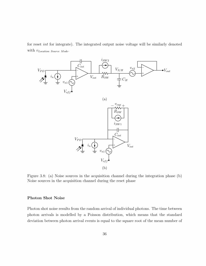
for reset int for integrate). The integrated output noise voltage will be similarly denoted
with vLocation Source Mode.
VPD
in
−
+ Vintvn1
Voff
RSW
iSW2
VS/H
CH
vn2 −
+Vout
Cint
(a)
VPD
in
−
+ Vintvn1
Voff
Cint
RSW
+vcap−
iSW1
(b)
Figure 3.8: (a) Noise sources in the acquisition channel during the integration phase (b)Noise sources in the acquisition channel during the reset phase
Photon Shot Noise
Photon shot noise results from the random arrival of individual photons. The time between
photon arrivals is modelled by a Poisson distribution, which means that the standard
deviation between photon arrival events is equal to the square root of the mean number of
36
photons per counting period [21]. The shot noise current PSD, denoted by in2
in Figure
3.8a is described by:
in2
= 2 · e−I = 2 · e−PPD · resp (3.32)
where e− is the charge of an electron, I is the average current, PPD is the average power
and resp is the photodiode responsivity. In the limit of detection, PPD is expected to be
dominated by the background excitation light and thus, PPD = PB. Substituting Eq. 3.1
in to Eq. 3.32 results in:
in2
= 2 · e−ILED · APD · LCEB · 10−ODB · resp (3.33)
Since the photon shot noise source is located at the same point in the circuit as the
input signal, the output referred noise voltage PSD can be found using Eq. 3.24 as follows:
Sintout in(f) =
∥∥∥∥∥∥TintCint
∞∑p=−∞
sinc(
(f − pTs
) · Tint)
1 + j2π(f − pTs
) ·RSWCH·
A(f − pTs
)
A(f − pTs
) + 1
∥∥∥∥∥∥2
· in2 (3.34)
During the reset phase, the shot noise undergoes the same interference effect as the
photodiode signal described in Eq. 3.31. As the circuit is only in reset for a fraction of
the sampling period, the output voltage PSD is scaled by the reset duty cycle. The output
shot noise PSD will therefore also contribute:
Srsout in(f) =ThTs·∥∥∥∥∥∞∑
p=−∞
1
1 + j2πfpRSWCh·(
A(fp)
A(fp) + 1
)2
· RSW
1 + j2πfpRSWCint
∥∥∥∥∥2
· in2
(3.35)
Photodiode Noise
The photodiode contributes dark current shot noise and thermal noise to the output of the
signal acquisition channel. The dark current shot noise differs from the photon shot noise
discussed before in terms of the source of the current. The dark current of the photodiode
37
is an intrinsic DC current resulting from random generation of electron/hole pairs and is
a function of the photodiode area [58]. The dark current shot noise PSD is described by:
in2
= 2 · e−IDark = 2 · e− · ρDark · APD (3.36)
where ρDark is the dark current per unit area and APD is the area of the photodiode.
The thermal noise current PSD of the photodiode is a function of the diode resistance
RPD and is given by:
in2
=4 · k · TRPD
(3.37)
where k is the Boltzmann constant and T is the temperature.
Both of these noise sources are introduced as a current source in parallel with the
photodiode. Thus both of these noise sources will be subject to the same frequency shaping
as for the photon shot noise described in Eq. 3.34 and Eq. 3.35.
CTIA Op-amp Noise
The FCC op-amp used in the signal acquisition channel has an input referred noise vn PSD
made up of thermal and flicker noise. The full description and derivation of this noise is
provided in Appendix A.3. The op-amp noise contributes to both the reset phase noise
and the integration phase noise.
During reset, vn1 contributes to the random initial condition of Vcap as shown in Figure
3.8b. The transfer function from the op-amp input terminal to the integrating capacitor
during reset can be described by:
Vcap(f)
vn1(f)=
A(f)(1 + j2πRSW (Cint + CPD))
(A(f) + 1)(1 + j2πCintRSW ) + j2πRSWCPD(3.38)
As a result of the periodic switching between the reset and integrate modes, the actual noise
stored on Vcap is scaled by the reset duty cycle. The output-referred noise voltage PSD
from this capacitor follows the same transfer function as described by Eq. 3.30, resulting
38
in the output noise voltage PSD being described by:
Srsoutvn1(f) =
ThTs·
∥∥∥∥∥∥∞∑
p=−∞
Vcap(f − pTs
)
1 + j2π(f − pTs
)RSWCh
(A(f − p
Ts)
A(f − pTs
) + 1
)2∥∥∥∥∥∥2
(3.39)
During the integration phase, the CTIA op-amp noise is driven out through the S/H
circuit and to the output as shown in Figure 3.8a. The transfer function from vn1 to VS/H
is described by:
VS/H(f)
vn1(f)=
A(f) · (1 + ZPD · s · Cint)1 + (A(f) + 1) · ZPD · s · Cint
· 1
1 +RSWCHs(3.40)
Due to the periodic switching, the magnitude of the ADC sampled output referred noise
PSD is scaled by the integration mode duty cycle. When the capacitor value is sampled
by opening the S/H transmission gate and sampled again by the ADC it results in the
output-referred noise voltage PSD described by:
Sintoutvn1(f) =
TintTs·
∥∥∥∥∥∥∞∑
p=−∞
(A(f − p
Ts)
A(f − pTs
) + 1
)2
·(
1 +CPDCint
)·
vn1(f − pTs
)
1 + j2π(f − pTs
)RSWCh
∥∥∥∥∥∥2
(3.41)
Reset Transmission Gate Noise
The transmission gate noise is made up primarily of thermal noise. Minimal flicker noise
is present as the current flowing through the transistor is very small. The total current
noise PSD is described by:
iSW12
=8
3· k · T · (gm + gds + gmb) (3.42)
where: gm, gds, and gmb are all small signal parameters of the transistor; k is the Boltzmann
constant; and T is the temperature. This noise current results in a voltage across the
39

integrating capacitor during the reset phase that is given by:
Vcap(f) =RSW (A(f) + 1)
j2πfCPDRSW + (A(f) + 1)(j2πfRSWCint + 1)· iSW1 (3.43)
This offset is then transformed by the magnitude squared of Eq. 3.30, scaled by the duty
cycle of the reset mode, as described by:
SoutiSW1R(f) =ThTs·
∥∥∥∥∥∥∞∑
p=−∞
Vcap(f − pTs
)
1 + j2π(f − pTs
)RSWCh
(A(f − p
Ts)
A(f − pTs
) + 1
)2∥∥∥∥∥∥2
(3.44)
where fp = f − p/Ts.The noise contribution during the integration phase is negligible as the values of gm,
gds, and gmb are extremely small.
Sample and Hold Transmission Gate Noise
The noise contributed by the S/H transmission gate during the sample/integration stage
is represented by iSW2. The value of iSW2 follows the same relationship as in Eq. 3.42.
The transfer function to refer this to a voltage PSD across the S/H capacitor is described
by:
VS/H2 =
∥∥∥∥ RSW
1 + sCHRSW
∥∥∥∥2 · iSW22
(3.45)
This noise is scaled by the integration mode duty cycle and then output referred by:
SintoutiSW2(f) =
TintTs·∥∥∥∥∥∞∑
p=−∞
A(f − pTs
)
A(f − pTs
) + 1
RSW
1 + j2π(f − pTs
)CHRSW
∥∥∥∥∥2
· iSW22
(3.46)
Output Buffer Op-amp Noise
The output buffer noise needs to be treated a little differently because this noise source is
not switched. It is simply added to all signals presented to the output. Taking the input
40
referred noise of the op-amp as calculated in Appendix A.3, it is possible to calculate the
resulting output noise from a unity feedback configuration. By placing the op-amp in unity
feedback the output noise PSD is described by:
Sint rsoutvn2(f) =
∥∥∥∥∥∞∑
p=−∞
A(f − pTs
)
A(f − pTs
) + 1· vn2(f −
p
Ts)
∥∥∥∥∥2
(3.47)
3.2.6 Component design
The design choices for the various circuit components are made based on the parametrized
equations from the previous sections. To minimize the chances of mistakes, the previously
submitted folded cascode op-amp is used for both the output buffer and the CTIA. The
analysis of this op-amp is available in Appendix A. This limits the design choices required
to the sizing of: Cint, Ch and the transmission gate transistors. To limit complexity, the
same transmission gate sizing will be used for both the S/H and the CTIA reset gates.
CTIA
As was shown in Section 3.2.2 the gain of the integrator is tied to two parameters: the
integration period and the capacitor size. As was discussed in Section 3.1, the baseline
current from the excitation light is expected to be 116 nA. To accommodate variation in
the excitation intensity and possibly highly concentrated fluorescent samples, the capacitor
will be sized to allow for integration of currents up to 130nA without saturating.
Although the bandwidth of these signals is fairly low (10-50Hz), a sampling rate of 4
kHz was selected to help keep the capacitor size low. The AMSP35 technology is a 3.3V
process and thus the integrator will saturate at this voltage. Assuming a DC input signal,
integration time of Tint = 250µs, and a maximum integration range of 3.3V, the capacitor
value needs to be 9.85pF based on Eq. 3.7. To keep things simple, this value was rounded
up to 10pF.
41
Transmission Gate
The two transmission gates in the acquisition channel must facilitate fast reset of the CTIA
capacitor, high bandwidth transmission for the S/H. The bandwidth of the S/H can also
be adjusted by the sizing of Ch, thus the speed of the CTIA reset is the primary constraint.
The CTIA integrating capacitor was sized to be 10pF in the section above, thus the
transmission gate resistance must be low enough that several RC time constants can pass
without interfering with the 4kHz sampling rate. Five time constants(τ) are sufficient to
return the voltage to less than 1% of the reset value. By placing the requirement that 5τ
must pass in less than 1µs , RSW must satisfy:
5 ·RSW · Cint < 1µs (3.48)
RSW < 20kΩ (3.49)
Using the transmission gate resistance equations from [61], the gate resistance is described
by:
RSW = Rp||Rn (3.50)
Rn =Ln
µn · Cox ·Wn · (VDD − Vin − VTHN)(3.51)
Rp =Lp
µp · Cox ·Wp · (Vin − |VTHP |)(3.52)
where L and W are the dimensions of the transistor, VDD = 3.3V , VTHN and VTHP are
the transistor threshold voltages, µn and µp are the carrier mobilities and Cox is the gate
capacitance per unit area. For 1µm length and width of both transistors, the gate resistance
is estimated to be 3.9kΩ. In simulation the value of RSW = 1.67kΩ.
Sample and Hold
The sizing of the sample and hold capacitor determines the bandwidth of the signal allowed
to pass through to the output buffer. Using a small capacitor reduces the total foot print
42
used; however, giving a large capacitor helps reduce the noise. A value of Ch = 100fF
was selected as it is a compromise between small area and low noise. This sizing places
the 3dB frequency of the S/H at 953MHz; which is high enough to allow the photodiode
signal to propagate without attenuation.
3.3 Predicted System Performance
Using the parametrized equations and component sizing determined in the previous sec-
tions, this section will identify the total gain, noise output voltage PSD and system SNR
for the acquisition channel. By determining the SNR, the LOD of the system can be
determined and ways of improving the LOD can be identified.
3.3.1 Output Signal Magnitude
The output voltage magnitude of the acquisition channel is given by:
Vout(f) =TintCint
∞∑p=−∞
sinc(
(f − pTs
) · Tint)· IPD(f − p
Ts)
1 + j2π(f − pTs
) ·RSWCH·
A(f − pTs
)
A(f − pTs
) + 1(3.53)
as was described in Eq. 3.24. Taking the acquisition channel parameters given in Section
3.2.6 (summarized in Table 3.2), the output magnitude response for a given input frequency
is plotted in Figure 3.9.
By taking the photodiode current signal strengths predicted in Section 3.1, the total
output voltage is predicted to have 2.90V of baseline and 76µV of signal for a fluorophore
concentration of 10nM.
3.3.2 Total Output Noise
In the previous sections, the output noise PSD for the different noise sources in the signal
acquisition channel were calculated. The noise PSD provides insight into the profile of the
43
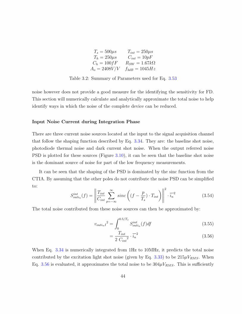
Ts = 500µs Tint = 250µsTh = 250µs Cint = 10pFCh = 100fF RSW = 1.67kΩAo = 2408V/V f3dB = 1045Hz
Table 3.2: Summary of Parameters used for Eq. 3.53
noise however does not provide a good measure for the identifying the sensitivity for FD.
This section will numerically calculate and analytically approximate the total noise to help
identify ways in which the noise of the complete device can be reduced.
Input Noise Current during Integration Phase
There are three current noise sources located at the input to the signal acquisition channel
that follow the shaping function described by Eq. 3.34. They are: the baseline shot noise,
photodiode thermal noise and dark current shot noise. When the output referred noise
PSD is plotted for these sources (Figure 3.10), it can be seen that the baseline shot noise
is the dominant source of noise for part of the low frequency measurements.
It can be seen that the shaping of the PSD is dominated by the sinc function from the
CTIA. By assuming that the other poles do not contribute the noise PSD can be simplified
to:
Sintoutin(f) =
∥∥∥∥∥TintCint
∞∑p=−∞
sinc
((f − p
Ts) · Tint
)∥∥∥∥∥2
· in2 (3.54)
The total noise contributed from these noise sources can then be approximated by:
voutinI2 =
∫ 0.5/Ts
0
Sintoutin(f)df (3.55)
=Tint
2 Cint2 · in
2(3.56)
When Eq. 3.34 is numerically integrated from 1Hz to 10MHz, it predicts the total noise
contributed by the excitation light shot noise (given by Eq. 3.33) to be 215µVRMS. When
Eq. 3.56 is evaluated, it approximates the total noise to be 304µVRMS. This is sufficiently
44
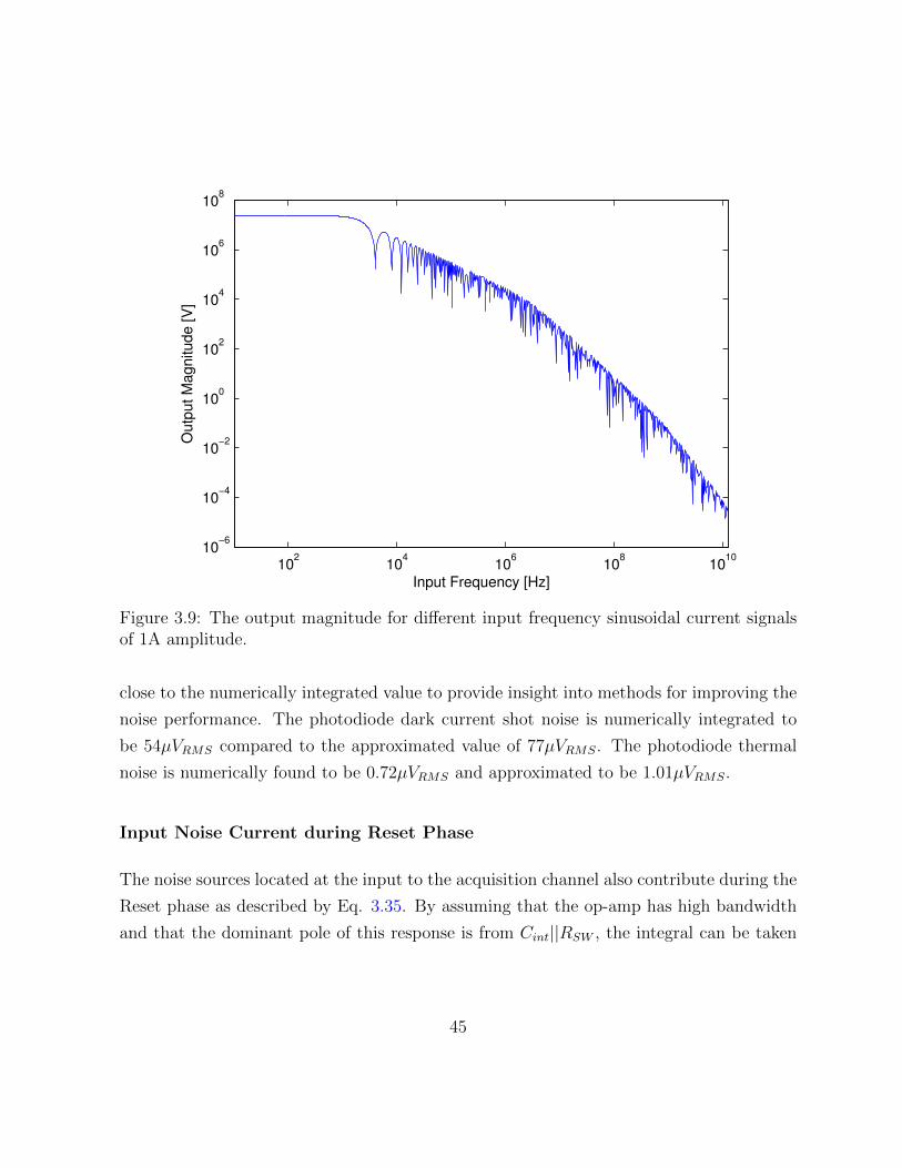
102
104
106
108
1010
10−6
10−4
10−2
100
102
104
106
108
Input Frequency [Hz]
Outp
ut M
agnitude [V
]
Figure 3.9: The output magnitude for different input frequency sinusoidal current signalsof 1A amplitude.
close to the numerically integrated value to provide insight into methods for improving the
noise performance. The photodiode dark current shot noise is numerically integrated to
be 54µVRMS compared to the approximated value of 77µVRMS. The photodiode thermal
noise is numerically found to be 0.72µVRMS and approximated to be 1.01µVRMS.
Input Noise Current during Reset Phase
The noise sources located at the input to the acquisition channel also contribute during the
Reset phase as described by Eq. 3.35. By assuming that the op-amp has high bandwidth
and that the dominant pole of this response is from Cint||RSW , the integral can be taken
45
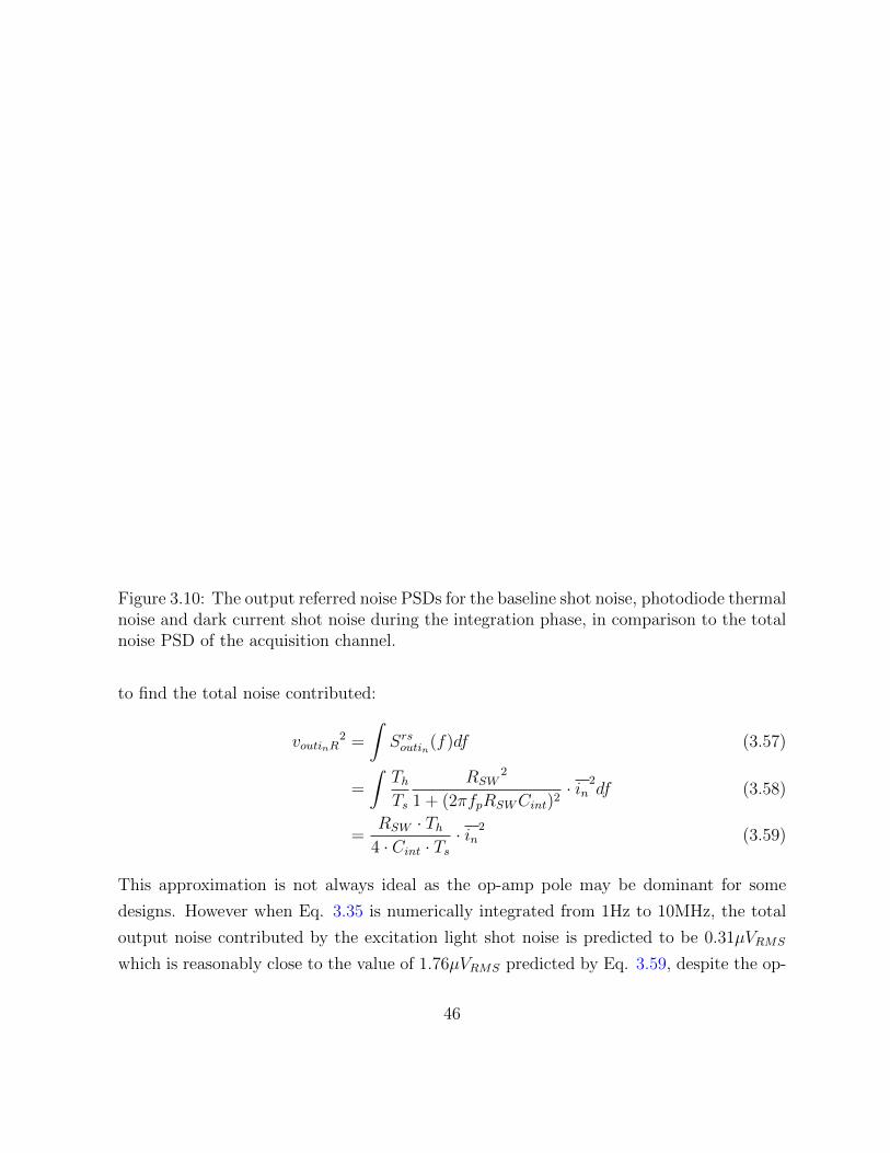
Figure 3.10: The output referred noise PSDs for the baseline shot noise, photodiode thermalnoise and dark current shot noise during the integration phase, in comparison to the totalnoise PSD of the acquisition channel.
to find the total noise contributed:
voutinR2 =
∫Srsoutin(f)df (3.57)
=
∫ThTs
RSW2
1 + (2πfpRSWCint)2· in2df (3.58)
=RSW · Th
4 · Cint · Ts· in2 (3.59)
This approximation is not always ideal as the op-amp pole may be dominant for some
designs. However when Eq. 3.35 is numerically integrated from 1Hz to 10MHz, the total
output noise contributed by the excitation light shot noise is predicted to be 0.31µVRMS
which is reasonably close to the value of 1.76µVRMS predicted by Eq. 3.59, despite the op-
46

amp being the dominant pole in this configuration. Similarly, the integrated value for the
photodiode dark current shot noise during reset is calculated to be 0.079µVRMS, compared
to the approximated value of 0.44µVRMS. The integrated value for the photodiode thermal
noise during reset is calculated to be 1.04nVRMS and the approximated calculation predicts
5.88nVRMS. As can be seen in Figure 3.11, the total noise contributed by these sources
during the reset phase is insignificant compared to their contribution during the integration
phase.
Figure 3.11: The output referred noise PSDs for the baseline shot noise, photodiode thermalnoise and dark current shot noise during the reset phase, in comparison to the total noisePSD of the acquisition channel.
47
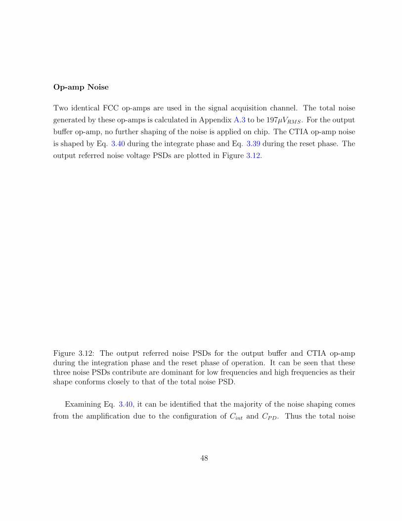
Op-amp Noise
Two identical FCC op-amps are used in the signal acquisition channel. The total noise
generated by these op-amps is calculated in Appendix A.3 to be 197µVRMS. For the output
buffer op-amp, no further shaping of the noise is applied on chip. The CTIA op-amp noise
is shaped by Eq. 3.40 during the integrate phase and Eq. 3.39 during the reset phase. The
output referred noise voltage PSDs are plotted in Figure 3.12.
Figure 3.12: The output referred noise PSDs for the output buffer and CTIA op-ampduring the integration phase and the reset phase of operation. It can be seen that thesethree noise PSDs contribute are dominant for low frequencies and high frequencies as theirshape conforms closely to that of the total noise PSD.
Examining Eq. 3.40, it can be identified that the majority of the noise shaping comes
from the amplification due to the configuration of Cint and CPD. Thus the total noise
48

contributed during the integrate phase can be approximated to:
voutvn1I2 =
TintTs· (1 +
CPDCint
) · vn12 (3.60)
where vn1 is the input referred noise of the op-amp. Similarly, an examination of Eq. 3.39
shows that the transformations of the noise are effectively unity until a bandwidth beyond
the 3dB of the amplifier, allowing the output referred noise to be summarized by:
voutvn1R2 =
ThTs· vn12 (3.61)
Comparison between the numerically calculated (between 1Hz and 10MHz) integration
phase noise from the CTIA op-amp and the approximated calculation provide values of
134µVRMS and 130µVRMS respectively. For the CTIA op-amp noise during reset provide
an numerically calculated value of 90.4µVRMS and an approximated value of 98.6µVRMS.
Switch Noise
There are two transmission gates in the acquisition channel that contribute noise. The
reset switch for the CTIA has a noise PSD described by Eq. 3.44. The S/H switch has an
output referred noise PSD described by Eq. 3.46. When plotted it can easily be seen that
these switches contribute negligibly to the total output noise (Figure 3.13). Examining the
reset switch noise PSD, it can be seen that if the the RSW ||Cint pole is dominant, the total
noise contributed is effectively time averaged kT/C noise:
voutiSW1R2 =
ThTs
RSW
4CintiSW1
2(3.62)
=ThTs· 2kT
3Cint(3.63)
Similarly for the S/H switch, if the dominant pole is assumed to be from RSW ||Ch, the
total output noise is:
voutiSW2I2 =
TintTs· 2kT
3Ch(3.64)
49

When comparing the numerically integrated results to the approximated equations, the
reset switch numerically works out to 5.1µVRMS compared to the approximated value of
11.7µVRMS. The S/H switch numerically is calculated to be 7.33µVRMS compared to the
approximated value of 114µVRMS. The large difference between the values for the S/H
switch is because the assumption that Ch is violated as the unity gain frequency of the
output buffer is much less then the S/H pole.
Figure 3.13: The output referred noise PSDs for the reset and S/H switches. Both thesenoise sources do not contribute significantly to the total output noise PSD profile.
3.3.3 Limit of Detection
The metric by which LOC FD is compared is the LOD. The LOD is determined as the
fluorophore concentration at which the fluorescent signal falls below three times the mea-
surement noise floor [62].
50

Source Noise Contribution [µVRMS]Integration Phase Excitation Light Shot Noise 215Integration Phase Photodiode Dark Current Shot Noise 54.2Integration Phase Photodiode Thermal Noise 0.72Reset Phase Excitation Light Shot Noise 30.5Reset Phase Photodiode Dark Current Shot Noise 0.142Reset Phase Photodiode Thermal Noise 0.0018Output Buffer 197CTIA Op-amp Integration Phase 134CTIA Op-amp Reset Phase 90.4Reset Transmission Gate 5.10Sample and Hold Transmission Gate Noise 7.33
Total Noise 338µVRMS
Table 3.3: The summation of the noise sources present in the acquisition channel.
The optical signal strength in this case is only that resulting from the fluorescence.
The measured excitation signal is constant and can easily be removed. The optical signal
strength for the proposed FD device is described by Eq. 3.2. Assuming that the frequency
components of IPD are small compared to the integration time, the voltage output signal
for this device is described by:
Vsig =TintCint· resp · ILED · ACh · LCEFl · 10−ODFl · ln(10) · ε · d · φ · c (3.65)
The noise in the measurement signal has been derived in the previous section. The noise
can be approximated by the following equation:
Vn2 = voutinI
2 + voutinR2 + voutvn1I
2 + voutvn1R2 + voutvn2IR
2 + voutiSW1R2 + voutiSW2I
2 (3.66)
The LOD is defined in terms of SNR, as the point where the fluorophore concentration
results in:
SNR = 3 =Vsig
2
Vn2 (3.67)
51
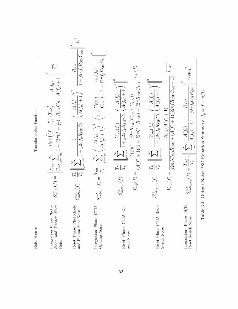
Noi
seS
ourc
eT
ran
sform
ati
on
Fu
nct
ion
Inte
grat
ion
Ph
ase
Ph
oto-
dio
de
and
Ph
oton
Sh
otN
oise
Sint
outin(f
)=
∥ ∥ ∥ ∥ ∥ ∥Tint
Cint
∞ ∑p=−∞
sinc( (f−
p Ts)·T
int)
1+j2π
(f−
p Ts)·R
SWCH
·A
(fp)
A(fp)
+1
∥ ∥ ∥ ∥ ∥ ∥2
·in2
Res
etP
has
eP
hot
od
iod
ean
dP
hot
onSh
otN
oise
Srsoutin(f
)=Th
Ts
·∥ ∥ ∥ ∥ ∥∞ ∑p=−∞
1
1+j2πf pRSWCh
·( A(fp)
A(fp)
+1
) 2 ·RSW
1+j2πf pRSWCint
∥ ∥ ∥ ∥ ∥2
·i n2
Inte
grat
ion
Ph
ase
CT
IAO
p-a
mp
Noi
seSint
outv
n1(f
)=Tint
Ts
·∥ ∥ ∥ ∥ ∥∞ ∑p=−∞
( A(fp)
A(fp)
+1
) 2 ·( 1+CPD
Cint
) ·v n
1(fp)
1+j2πf pRSWCh
∥ ∥ ∥ ∥ ∥2
Res
etP
has
eC
TIA
Op
-am
pN
oise
Srsoutv
n1(f
)=Th
Ts
·∥ ∥ ∥ ∥ ∥∞ ∑p=−∞
Vcap(fp)
1+j2πf pRSWCh
( A(fp)
A(fp)
+1
) 2∥ ∥ ∥ ∥ ∥2
Vcap(f
)=
A(f
)(1
+j2πRSW
(Cint+CPD
))
(A(f
)+
1)(1
+j2πCintR
SW
)+j2πRSWCPD
·vn1(f
)
Res
etP
has
eC
TIA
Res
etS
wit
chN
oise
SrsoutiSW
1(f
)=Th
Ts
·∥ ∥ ∥ ∥ ∥∞ ∑p=−∞
Vcap(fp)
1+j2πf pRSWCh
( A(fp)
A(fp)
+1
) 2∥ ∥ ∥ ∥ ∥2
Vcap(f
)=
RSW
(A(f
)+
1)
j2πfCPDRSW
+(A
(f)
+1)
(j2πfRSWCint+
1)·iSW
1
Inte
grat
ion
Ph
ase
S/H
Res
etSw
itch
Noi
seSint
outiSW
2(f
)=Tint
Ts
·∥ ∥ ∥ ∥ ∥∞ ∑p=−∞
A(fp)
A(fp)
+1
RSW
1+j2πf pCHRSW
∥ ∥ ∥ ∥ ∥2
·iSW
22
Tab
le3.
4:O
utp
ut
Noi
seP
SD
Equat
ion
Sum
mar
y.f p
=f−p/Ts
52

Noise Source Noise PSD Equation
Excitation Light Photon ShotNoise
in2
= 2 · e−ILED · APD · LCEB · 10−ODB · resp
Photodiode Dark Current ShotNoise
in2
= 2 · e−IDark = 2 · e− · ρDark · APD
Photodiode Thermal Noisein
2=
4 · k · TRPD
Folded Cascode Op-amp Noisevn1
2 = vn22 =
2
gmN22· (InN2
2 + InN10
2 + 2 · InP4
2) · 1A(f)2
In2
=Kf · IdAFCox · w · l
· 1
f+
8
3· k · T · (gm + gds + gmb)
Transmission Gate Switch Noise iSW2
=8
3· k · T · (gm + gds + gmb)
Table 3.5: Noise Input Equations
which can then be manipulated into:
cLOD =
√3 · Vn · Cint
Tint · resp · ILED · ACh · LCEFl · 10−ODFl · ln(10) · ε · d · φ (3.68)
In this form a sensitivity analysis can be performed to identify parameters which can
be optimized to improve the LOD. Some interesting parameters to examine are: APD, Tint,
Cint and vn1+n2. When the photodiode area is increased, a minimum is seen where the
increased light collection efficiency is eventually over come by the increased baseline light
collected resulting in a larger shot noise component (Figure 3.14a). This result proposes
that there is an optimal size for the photodiode for LOC FD.
By decreasing the op-amp noise by a factor of 10, it the op-amp no longer contributes
meaningfully to the total noise and no further advantage is received (Figure 3.14b). Sim-
ilarly for the value of Cint, by decreasing its value an increase in signal gain is achieved
however for values much below 10pF, the dominant source of noise becomes the op-amp
53
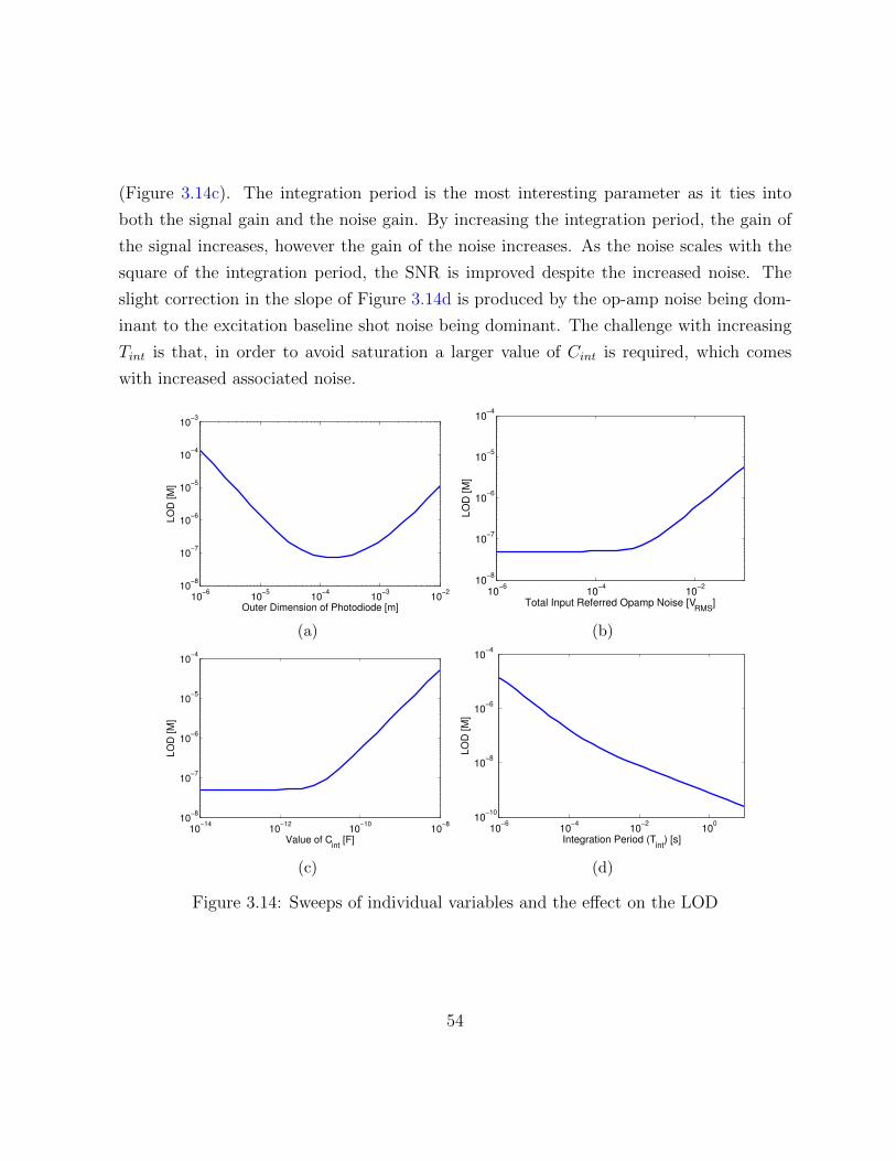
(Figure 3.14c). The integration period is the most interesting parameter as it ties into
both the signal gain and the noise gain. By increasing the integration period, the gain of
the signal increases, however the gain of the noise increases. As the noise scales with the
square of the integration period, the SNR is improved despite the increased noise. The
slight correction in the slope of Figure 3.14d is produced by the op-amp noise being dom-
inant to the excitation baseline shot noise being dominant. The challenge with increasing
Tint is that, in order to avoid saturation a larger value of Cint is required, which comes
with increased associated noise.
10−6
10−5
10−4
10−3
10−2
10−8
10−7
10−6
10−5
10−4
10−3
LO
D [M
]
Outer Dimension of Photodiode [m]
(a)
10−6
10−4
10−2
10−8
10−7
10−6
10−5
10−4
LO
D [
M]
Total Input Referred Opamp Noise [VRMS
]
(b)
10−14
10−12
10−10
10−8
10−8
10−7
10−6
10−5
10−4
LO
D [M
]
Value of Cint
[F]
(c)
10−6
10−4
10−2
100
10−10
10−8
10−6
10−4
LO
D [
M]
Integration Period (Tint
) [s]
(d)
Figure 3.14: Sweeps of individual variables and the effect on the LOD
54

Chapter 4
Circuit Simulation Results
To validate the equations derived in Chapter 3 the acquisition channel circuits are simulated
using the AMSP35 v4.00 kit from CMC. The simulations are done using SpectreRF from
Cadence. The following sections simulate the acquisition channel to observe: the integrator
transfer function, the interference models, and the predicted output noise PSD.
4.1 Simulations of Acquisition Channel
The following simulations of the CTIA, S/H and output buffer demonstrate good agreement
between the predicted frequency domain output and the analysis results derived in Chapter
3. The simulated time-domain output signals are also in good agreement with the expected
(Figure 3.2b) outputs, as demonstrated in Figure 4.1.
4.1.1 Behavioural Simulations
The equations derived in Chapter 3 are formed around idealized approximations of switches
and op-amp functions. To verify that these equations are correct, an idealized implemen-
tation of the acquisition channel is simulated. This allows for validation of the models
55
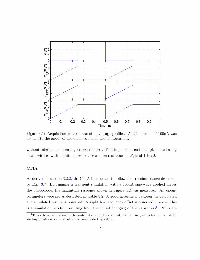
0
1
2
3 φ
[V
]
0
1
2
3
Vin
t(t)
[V]
0
1
2
3
VS
nH
(t)
[V]
0 0.1 0.2 0.3 0.4 0.5 0.6 0.7 0.8 0.9 10
1
2
3
Vout(t
) [V
]
Time [ms]
Figure 4.1: Acquisition channel transient voltage profiles. A DC current of 100nA wasapplied to the anode of the diode to model the photocurrent.
without interference from higher order effects. The simplified circuit is implemented using
ideal switches with infinite off resistance and on resistance of RSW of 1.76kΩ.
CTIA
As derived in section 3.2.2, the CTIA is expected to follow the transimpedance described
by Eq. 3.7. By running a transient simulation with a 100nA sine-wave applied across
the photodiode, the magnitude response shown in Figure 4.2 was measured. All circuit
parameters were set as described in Table 3.2. A good agreement between the calculated
and simulated results is observed. A slight low frequency offset is observed, however this
is a simulation artefact resulting from the initial charging of the capacitors1. Nulls are
1This artefact is because of the switched nature of the circuit, the DC analysis to find the simulatorstarting points does not calculate the correct starting values.
56
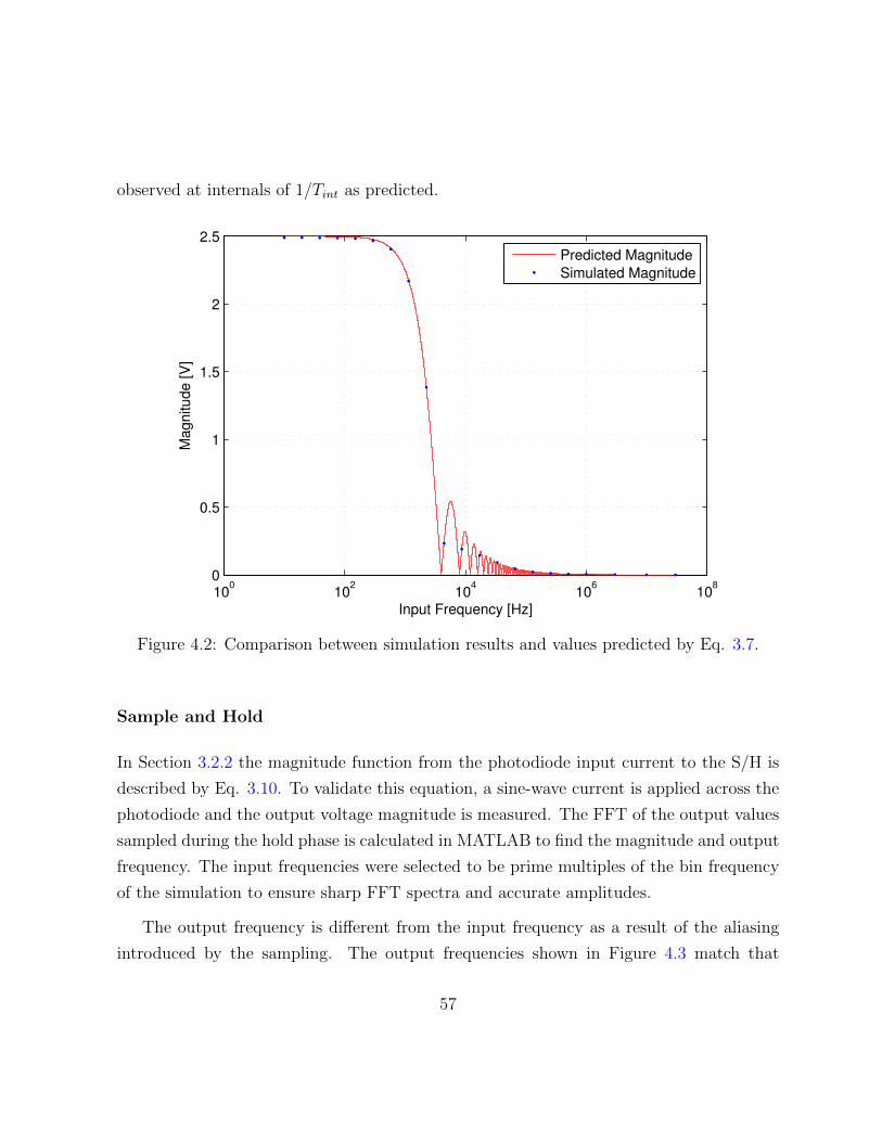
observed at internals of 1/Tint as predicted.
100
102
104
106
108
0
0.5
1
1.5
2
2.5
Input Frequency [Hz]
Magnitu
de
[V
]
Predicted Magnitude
Simulated Magnitude
Figure 4.2: Comparison between simulation results and values predicted by Eq. 3.7.
Sample and Hold
In Section 3.2.2 the magnitude function from the photodiode input current to the S/H is
described by Eq. 3.10. To validate this equation, a sine-wave current is applied across the
photodiode and the output voltage magnitude is measured. The FFT of the output values
sampled during the hold phase is calculated in MATLAB to find the magnitude and output
frequency. The input frequencies were selected to be prime multiples of the bin frequency
of the simulation to ensure sharp FFT spectra and accurate amplitudes.
The output frequency is different from the input frequency as a result of the aliasing
introduced by the sampling. The output frequencies shown in Figure 4.3 match that
57
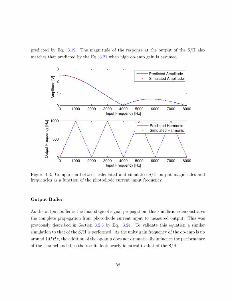
predicted by Eq. 3.19. The magnitude of the response at the output of the S/H also
matches that predicted by the Eq. 3.21 when high op-amp gain is assumed.
0 1000 2000 3000 4000 5000 6000 7000 80000
1
2
3
Input Frequency [Hz]
Am
plit
ude [V
]
0 1000 2000 3000 4000 5000 6000 7000 80000
500
1000
Input Frequency [Hz]
Ou
tput F
requency [H
z]
Predicted Amplitude
Simulated Amplitude
Predicted Harmonic
Simulated Harmonic
Figure 4.3: Comparison between calculated and simulated S/H output magnitudes andfrequencies as a function of the photodiode current input frequency.
Output Buffer
As the output buffer is the final stage of signal propagation, this simulation demonstrates
the complete propagation from photodiode current input to measured output. This was
previously described in Section 3.2.3 by Eq. 3.24. To validate this equation a similar
simulation to that of the S/H is performed. As the unity gain frequency of the op-amp is up
around 1MHz, the addition of the op-amp does not dramatically influence the performance
of the channel and thus the results look nearly identical to that of the S/H.
58

4.1.2 Transistor Level Circuit Simulations
To further validate the mathematical model derived for the signal acquisition channel,
transistor level and extracted simulations of the complete circuit are performed. The tran-
sistor level simulations differ from the behavioural simulations in the non-ideal op-amp, the
pass transistor gate switches and physical diode characteristics. The extracted simulations
are performed on the calibre layout extracted equivalent circuit. This simulation should
provide the results closest to the physical implementation.
The FCC op-amp used for both the CTIA and output buffer is also simulated. The FCC
gain was simulated to be AV = 2511V/V with the corner frequency at f3dB = 100kHz,
placing Rout = 162MΩ and gm = 19.5µS. The complete results are in Appendix A.
The behavioural acquisition channel model simulations demonstrated that the transfer
functions derived in Section 3 provide a valid mathematical representation of the circuit.
The transistor level simulations will not match as closely as the ideal circuit models as these
simulations take into account the FCC op-amp characteristics as well as charge injection,
off resistance of the pass transistors and various other circuit effects. To allow proper
operation of the circuit, an offset voltage of 0.7V needs to be applied to the non-inverting
terminal of the FCC op-amp. This is due to the NMOS input transistors. Additionally,
photodiodes can only drive photo-current from the anode to the cathode, thus a DC bias
current must be applied in addition to any sine-waves. For these simulations a 50nA
DC current with a 50nA sine component will be applied to the anode of the photodiode.
Running the signal acquisition channel under this modified context, the circuit transfer
function demonstrates good agreement with the simplified simulations, as demonstrated in
Figure 4.4.
The introduction of the FCC op-amp introduces harmonic distortion as the output of
the integrator approaches the power rails. It can be seen in Figure 4.4 that the op-amp does
not drive the output to 3.2V as expected by the behavioural simulation but instead distorts
the sine-wave to a maximum value of roughly 2.7Vs. This is due to the PMOS cascode
transistor entering the triode region when the output voltage approaches the supply rail.
When examining the frequency domain response of the output this distortion can be seen
59

0 0.005 0.01 0.015 0.02 0.025 0.03 0.035 0.040.5
1
1.5
2
2.5
3
3.5
Time [s]
Vout(t
) [V
]Time domain Output Voltage
0 100 200 300 400 500 600 700 800 900 1000
10−5
100
Single−Sided Amplitude Spectrum
Frequency (Hz)
|Vout(f
)| [V
]
Transistor Level Simulation
Extracted Simulation
Simplified Circuit Simulation
Figure 4.4: Comparison of the sampled simplified circuit simulation results to the transistorlevel and extracted simulations. A 50nA, 113Hz sine-wave with a 50nA DC offset currentwas injected onto the photodiode for all three simulations. An integration time of 250µswas used with a total period of 500µs .
as extra tones at integer multiples of the input frequency. Higher-order harmonics can be
seen to be aliased down into the baseband as well.
There was good agreement between the transistor level simulation and the extracted
60

simulations. The extracted simulation demonstrated slightly less harmonic distortion as
the FCC op-amp didn’t clip the output until 2.8V however the harmonic distortion is still
a challenge which should be addressed in future iterations of the chip as this restricted
operating range of the amplifier reduces the total output range of the CTIA to only 2.1V.
4.2 Acquisition Channel Interference
There are two sources of signal interference which are discussed in Section 3.2.4: trans-
mission gate charge injection, and interference from the signal while the CTIA is in reset.
The following subsections will simulate these interference effects to validate their predicted
impact.
4.2.1 Charge Injection
Despite the design of the transmission gates to be matched PMOS and NMOS to allow for
charge cancellation, charge injection still takes place. The idealized model which suggests
that dummy transistors will sink all charge expelled by the transmission gate, does not
account for many of the higher order effects which are included in SpectreRF simulations.
However, the charge injection is a highly repeatable process and thus can be accounted for
during operation of the acquisition channel.
Of the two transmission gates used in this acquisition channel, only the S/H gate needs
to be accounted for. The gate located across the CTIA capacitor will inject charge equally
onto both sides of the gate. As equal charge is placed on either side of the capacitor, no
voltage is introduced. The S/H however injects charge on to Ch which is then buffered
off chip. Figure 4.5a demonstrates the addition of charge after the signal to close the
transmission gate is sent at t = Tint. The charge injection peaks at 11.4mV, however this
is mitigated down to 4.74mV as the dummy transistors begin to sink the excess charge.
This injection value is for Vint = 1.95V .
61

0 0.1 0.2 0.3 0.4 0.5 0.6 0.7 0.8 0.9 1−2
0
2
4
6
8
10
12
Time after SnH gate opens [µs]
VS
nH
(t)−
VS
nH
(Tin
t) [m
V]
(a)
0 0.5 1 1.5 2 2.5 30
2
4
6
8
10
12
14
Input Voltage [V]
∆ V
SnH
[m
V]
(b)
Figure 4.5: (a) Transient charge injection on VS/H for Vint = 1.95V . (b) Total chargeinjection onto output of S/H circuit in isolation, as a function of input voltage.
4.2.2 Signal Interference
As was described in Section 3.2.4, when in reset, the CTIA behaves like a conventional
TIA amplifier. As a result, when the CTIA comes out of reset, charge is sampled onto the
integrating capacitor. This charge is then propagated through the acquisition channel to
the output resulting in interference.
The magnitude of the voltage placed across the integrating capacitor is described by:
VCap(f)
IPD(f)=
ZSW · ZPD · (gm · Zo ·+1)
Zo · ZPD · gm + Zo + ZPD + ZSW(4.1)
where ZSW = RSW ||1/(sCint), ZPD = RPD||1/(sCPD) ≈ 1/(sCPD), Zo = Ro||1/(sCo) and
gm is the transconductance of the amplifier. At DC this equation reduces to:
VCap(f = 0)
IPD(f = 0)= RSW (4.2)
By running a transistor level DC simulation, the value of RSW was measured to be 2.165kΩ.
To evaluate the entire transimpedance function a transistor level AC simulation was per-
62
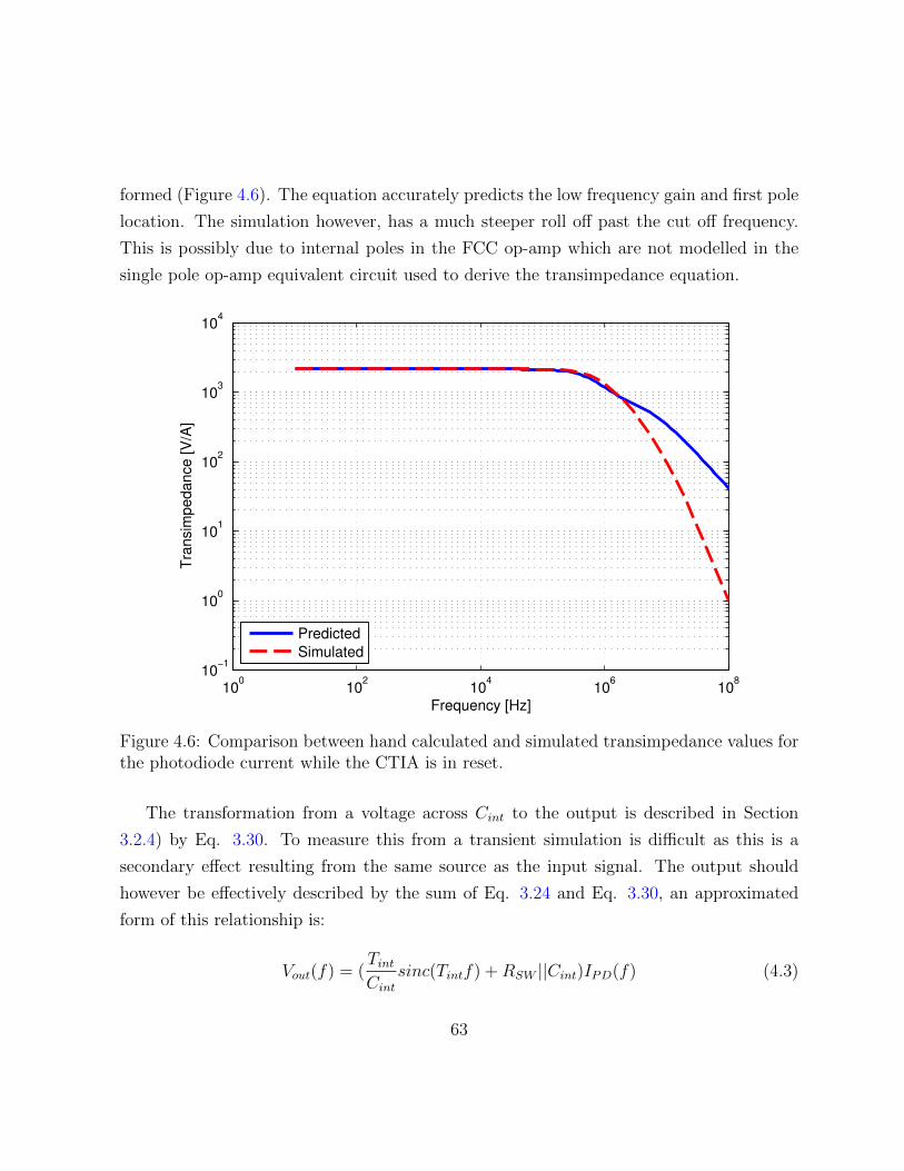
formed (Figure 4.6). The equation accurately predicts the low frequency gain and first pole
location. The simulation however, has a much steeper roll off past the cut off frequency.
This is possibly due to internal poles in the FCC op-amp which are not modelled in the
single pole op-amp equivalent circuit used to derive the transimpedance equation.
100
102
104
106
108
10−1
100
101
102
103
104
Frequency [Hz]
Tra
nsim
pedance [V
/A]
Predicted
Simulated
Figure 4.6: Comparison between hand calculated and simulated transimpedance values forthe photodiode current while the CTIA is in reset.
The transformation from a voltage across Cint to the output is described in Section
3.2.4) by Eq. 3.30. To measure this from a transient simulation is difficult as this is a
secondary effect resulting from the same source as the input signal. The output should
however be effectively described by the sum of Eq. 3.24 and Eq. 3.30, an approximated
form of this relationship is:
Vout(f) = (TintCint
sinc(Tintf) +RSW ||Cint)IPD(f) (4.3)
63

0 2000 4000 6000 8000 10000 12000 14000 16000 180000.024
0.026
0.028
0.03
0.032
0.034
0.036
Input Frequency [Hz]
Outp
ut M
agnitude [V
]
Predicted No Interference
Predicted with Interference
Simulated Reset Intereference
Figure 4.7: Comparison of integrator output for different current input frequencies, withand without accounting for the reset interference. It can be seen that the reset interferencedoes contribute to the output, however the derived model does not completely explain thehigher frequency effects taking place.
By making the integration time to be extremely small, the contribution from Eq. 3.24
will be small. As the interference is independent of timing parameters, the relative con-
tribution should increase. To make the influence more obvious, the reset switch resistance
is increased to 176kΩ. This is simulated using the behavioural model to minimize the
effects of other higher order effects. Figure 4.7 plots the simulated output described by
Eq. 4.3; it can be seen that there is good agreement is achieved for low frequency values,
however the equation begins to diverge as frequency increases. This is due to two poles
not properly accounted for in this equation: the photodiode capacitance and the op-amp
transfer function pole. These poles are also less significant when using the measured RSW
value.
64
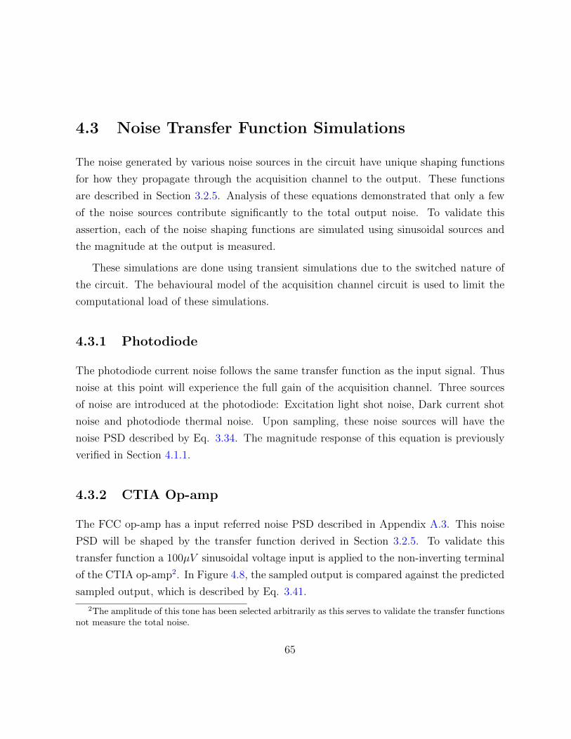
4.3 Noise Transfer Function Simulations
The noise generated by various noise sources in the circuit have unique shaping functions
for how they propagate through the acquisition channel to the output. These functions
are described in Section 3.2.5. Analysis of these equations demonstrated that only a few
of the noise sources contribute significantly to the total output noise. To validate this
assertion, each of the noise shaping functions are simulated using sinusoidal sources and
the magnitude at the output is measured.
These simulations are done using transient simulations due to the switched nature of
the circuit. The behavioural model of the acquisition channel circuit is used to limit the
computational load of these simulations.
4.3.1 Photodiode
The photodiode current noise follows the same transfer function as the input signal. Thus
noise at this point will experience the full gain of the acquisition channel. Three sources
of noise are introduced at the photodiode: Excitation light shot noise, Dark current shot
noise and photodiode thermal noise. Upon sampling, these noise sources will have the
noise PSD described by Eq. 3.34. The magnitude response of this equation is previously
verified in Section 4.1.1.
4.3.2 CTIA Op-amp
The FCC op-amp has a input referred noise PSD described in Appendix A.3. This noise
PSD will be shaped by the transfer function derived in Section 3.2.5. To validate this
transfer function a 100µV sinusoidal voltage input is applied to the non-inverting terminal
of the CTIA op-amp2. In Figure 4.8, the sampled output is compared against the predicted
sampled output, which is described by Eq. 3.41.
2The amplitude of this tone has been selected arbitrarily as this serves to validate the transfer functionsnot measure the total noise.
65
100
102
104
106
108
10−7
10−6
10−5
10−4
10−3
Input Frequency [Hz]
Vout(f
) [V
]
Predicted
Simulated
Figure 4.8: The amplitude of various input tones (Red dots) correspond to the amplitudeof that predicted by the transfer function.
Good agreement is seen between the predicted and simulated results. Some slight
deviation from the equation is observed in the lower frequencies; however, the corner
frequency corresponds are predicted.
4.3.3 CTIA Reset Transmission Gate
The thermal noise generated by the CTIA reset transmission gate does not introduce noise
during the integration phase as the values of gm and gds are too small to be significant.
During the reset phase however, the thermal noise PSD results in a reset noise (VCap)
being placed across Cint which is sampled when the CTIA returns to the integrate phase of
operation. The value of VCap is determined largely by the RC filter of the switch impedance
66

and the value of Cint, which is mathematically described by Eq. 3.43.
When the CTIA returns to the integrate phase, the noise across Cint is effectively
sampled and held. The held voltage is then propagated across the sample and hold register
and onto the output during the integration phase. The output signal is finally sampled
resulting in an output voltage magnitude described by Eq. 3.44.
100
102
104
106
108
10−11
10−10
10−9
10−8
10−7
Input Frequency [Hz]
Vout(f
) [V
]
Predicted
Simulated
Figure 4.9: The amplitude of various input tones (Red dots) correspond to the amplitudeof that predicted by the transfer function. The spectra for the highest frequency simulatedtone was not able to be plotted due to simulator related issues, however the magnitude ofthe sinusoid was measured from the transient Vout signal by hand.
Transient simulations of the behavioural circuit were performed to validate the pre-
dicted transimpedance function. These simulations were performed by applying an current
sine-wave of different frequencies an 10pA amplitude across the reset switch resistor with
ideal switches located on either side. The circuit was operated with a 250µs reset and in-
tegration period for a total period of 500µs . The Fourier transform was performed on the
67
data sampled from the output buffer during the reset phase. These simulations demon-
strated that the low frequency amplitudes and locations predicted by Eq. 3.44 match
closely with the output spectra. Figure 4.9 shows that the first pole is located slightly
lower than in simulation. To perform accurate simulations at such high frequencies how-
ever presents extremely large computational requirements. Despite error in the pole loca-
tion, the magnitude of the transimpedance demonstrate that the noise contributed during
the reset phase is not significant compared to the noise contributed during the integration
phase.
4.3.4 Sample and Hold Transmission Gate
Behaviourally, the sample and hold transmission gate behaves as a resistor during the
integration phase and as a open circuit during the reset phase. This was mathematically
described in Section 3.2.5 by Eq. 3.46.
This equation represents the transimpedance of the equivalent current noise of the
transmission gate to the output. To avoid running extremely large simulations, the tran-
simpedance function can be validated against a sinusoidal current input in parallel with
the transmission gate. Figure 4.10 plots the sampled output of the buffer against the in-
put frequency, demonstrating that Eq. 3.46 is in good agreement with the behavioural
simulations.
4.3.5 Output Buffer
The output buffer consists of the FCC op-amp in a unity feedback configuration. This
means that the noise contributed by this op-amp will be the equivalent of the input re-
ferred noise of the op-amp transformed by the unity gain function. Mathematically this is
described by:
SBuff (f) =
∥∥∥∥ A(f)
A(f) + 1
∥∥∥∥2 · SInput(f) (4.4)
68
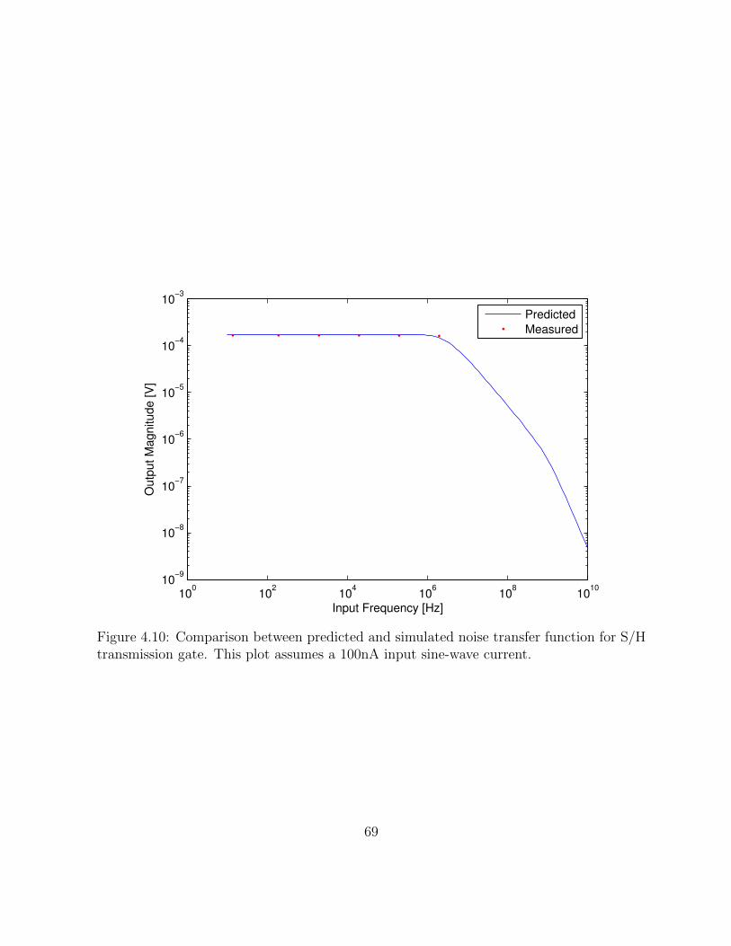
100
102
104
106
108
1010
10−9
10−8
10−7
10−6
10−5
10−4
10−3
Input Frequency [Hz]
Outp
ut M
agnitude [V
]
Predicted
Measured
Figure 4.10: Comparison between predicted and simulated noise transfer function for S/Htransmission gate. This plot assumes a 100nA input sine-wave current.
69
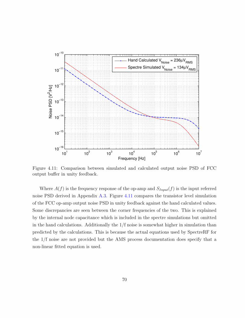
101
102
103
104
105
106
107
10−16
10−15
10−14
10−13
10−12
10−11
10−10
Frequency [Hz]
Nois
e P
SD
[V
2/H
z]
Hand Calculated VNoise
= 236µVRMS
Spectre Simulated VNoise
= 134µVRMS
Figure 4.11: Comparison between simulated and calculated output noise PSD of FCCoutput buffer in unity feedback.
Where A(f) is the frequency response of the op-amp and SInput(f) is the input referred
noise PSD derived in Appendix A.3. Figure 4.11 compares the transistor level simulation
of the FCC op-amp output noise PSD in unity feedback against the hand calculated values.
Some discrepancies are seen between the corner frequencies of the two. This is explained
by the internal node capacitance which is included in the spectre simulations but omitted
in the hand calculations. Additionally the 1/f noise is somewhat higher in simulation than
predicted by the calculations. This is because the actual equations used by SpectreRF for
the 1/f noise are not provided but the AMS process documentation does specify that a
non-linear fitted equation is used.
70
4.4 Transient Noise Simulations
The total noise of the measurement is the only noise value that matters when the LOD of
the device is determined. Section 3.3.2 determines that of the various noise sources, only
four contribute significantly to the total output noise: The integration phase excitation
light shot noise; the CTIA op-amp integration phase noise; the CTIA op-amp reset phase
noise; and the output buffer noise. The total noise contributed by the output buffer was
determined in Section 4.3.5. The transfer functions for the different noise sources were
validated in the previous section, however the total noise contribution is not determined.
This section will perform transient noise simulations on the behavioural model of the sig-
nal acquisition channel. The noise generated by the CTIA op-amp and the shot noise gen-
erated by the excitation photo-current are simulated. These results are compared against
the equations derived in Section 3.3.2.
4.4.1 CTIA Op-amp Transient Noise Simulation
The total output noise generated by the CTIA op-amp is comprised of two components:
that generated during the reset phase, and that generated during the integrate phase. As
these generate from a common source, the total output noise power will be described by
the sum of the powers of these signals:
voutvn1IR2 = voutvn1R
2 + voutvn1I2 (4.5)
where voutvn1I and voutvn1R are described by Eq. 3.60 and Eq. 3.61 respectively.
To simplify the simulation, a white thermal noise was assumed for the input referred
noise PSD. A value of 1.21 · 10−8V 2/Hz was assumed for the PSD amplitude. This value
was selected as it matched the thermal noise floor from the op-amp noise PSD simulations,
however it was realized later that this was a value for output referred noise instead of
input referred. This increases the total noise measured but the trend predicted by Eq. 4.5
71
should match. The 3dB bandwidth of the op-amp is estimated to be 1MHz. This provides
a rough total noise of the op-amp to be:
vn12 = 1.21 · 10−8
V 2
Hz· 1MHz = 0.0121V 2 (4.6)
The first simulation was run at FMAX = 10MHz as this is 10 times the maximum frequency
of the op-amp. FMIN = 3.9Hz as the this was one over the simulation period. The
simulation period was 256ms. Tint = 250µs and Th = 250µs for a Ts = 500µs. These
parameters give a predicted total noise of 128.8mVRMS. The simulated noise from the op-
amp for these parameters was measured to be 122mVRMS. To ensure that the simulation
was run for sufficient duration, the standard deviation of the output was plotted against
the number of samples in Figure 4.12. It can be seen that the noise converges to within
approximately 3% after 100 samples. Thus the simulation time will be reduced to 50ms.
The total noise generated for different values of Tint is simulated, with all other param-
eters are held constant (Ts = 500µs with Th adjusted). Figure 4.13a plots the predicted
and measured value of the noise. A divergence from the predicted trend is thought to be a
result of correlation between noise contributions during reset and integrate. In Eq. 4.5 the
two noise sources are assumed to be uncorrelated; however, examining the time domain
signal this can be thought of as a bad approximation. During reset, the output will be
described by:
Vout(t) = vn1(t) (4.7)
When the circuit returns to integrate mode at some time to, Eq. 4.7 is sampled onto the
capacitor Cint and added to the now amplified op-amp noise, as described by:
Vout(t) = vn1(to) + (1 +CpdCint
) · vn1(t) (4.8)
As a result, the noise sum of the two terms will be described by the autocorrelation of
vn1(t). When the model is modified to include a correlation coefficient, a 50% correlation
provides a good fit to the measured output noise, as shown in Figure 4.13a.
72

0 100 200 300 400 500 6000
0.02
0.04
0.06
0.08
0.1
0.12
0.14
0.16
Number of Samples
Sta
ndard
Devia
tion [V
RM
S]
Figure 4.12: The standard deviation of the sampled output as a function of the number ofsamples taken. It can be seen that 100 samples is sufficient to provide an accurate valuefor the standard deviation.
4.4.2 Photodiode Transient Noise Simulation
The total output noise of the acquisition channel that is generated by the photodiode is
described by Eq. 3.56. It was previously shown that the noise contributed during the
reset phase is negligible in comparison. To validate the noise predicted by Eq. 3.56, a
transient noise simulation is run. The photodiode noise is expected to be dominated by
the excitation light shot noise, thus the input noise will be described by the shot noise
equation. For a baseline current of 110nA, the input noise PSD is in2
= 3.52 ·10−26A2/Hz.
As was demonstrated by Figure 4.12 the measured noise is accurate after 100 samples,
for a sampling period of 500ms the simulation needs to be run for 50ms. The transient
noise simulation was run with a FMAX = 10MHz and FMIN = 10Hz. The simulations are
73
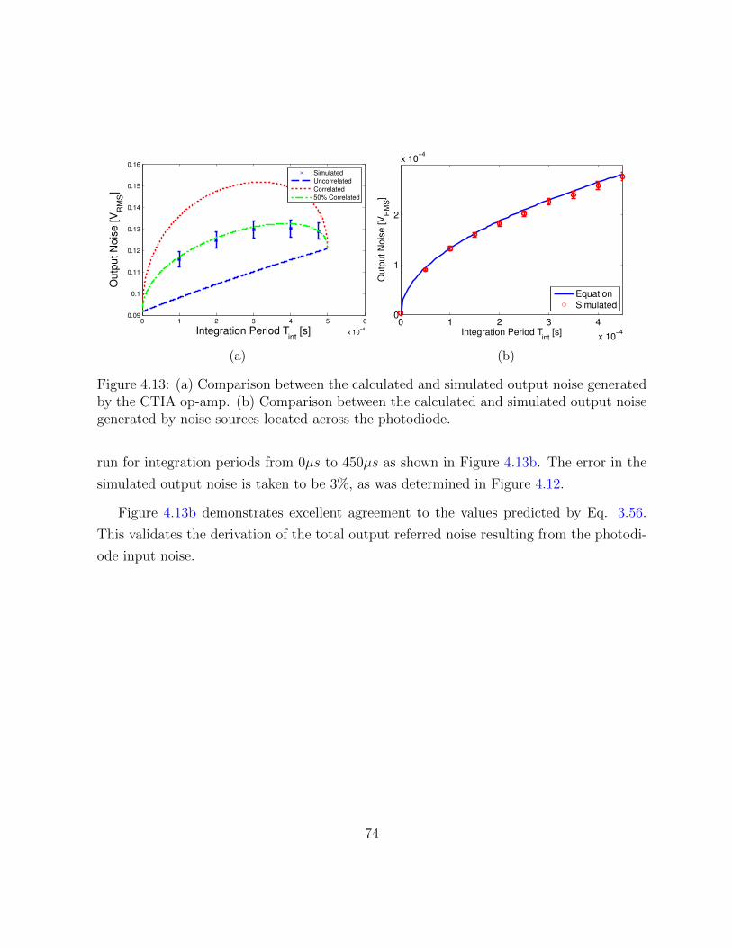
0 1 2 3 4 5 6
x 10−4
0.09
0.1
0.11
0.12
0.13
0.14
0.15
0.16
Integration Period Tint
[s]
Outp
ut N
ois
e [V
RM
S]
Simulated
Uncorrelated
Correlated
50% Correlated
(a)
0 1 2 3 4
x 10−4
0
1
2
x 10−4
Integration Period Tint
[s]
Outp
ut N
ois
e [V
RM
S]
Equation
Simulated
(b)
Figure 4.13: (a) Comparison between the calculated and simulated output noise generatedby the CTIA op-amp. (b) Comparison between the calculated and simulated output noisegenerated by noise sources located across the photodiode.
run for integration periods from 0µs to 450µs as shown in Figure 4.13b. The error in the
simulated output noise is taken to be 3%, as was determined in Figure 4.12.
Figure 4.13b demonstrates excellent agreement to the values predicted by Eq. 3.56.
This validates the derivation of the total output referred noise resulting from the photodi-
ode input noise.
74

Chapter 5
Experimental Results
This chapter describes the experimental results measured from the CMOS and a discrete
circuit implementation of the acquisition channel described and simulated in the previous
chapters. This chapter: outlines how each circuit was implemented, explains the test setup
for the measurements, and tries to validate the acquisition channel transfer functions and
noise analysis.
The CMOS and discrete implementations of the acquisition were initially developed
to allow for a comparison in the performance. Initial testing demonstrated several im-
plementation problems with the operation of CMOS of the circuit. This forces most of
the analysis to be on the discrete implementation, for which modifications to the noise
equations are needed. An effort is made to identify the reasons that the CMOS doesn’t
operate as expected however no exact cause has been identified.
5.1 ASIC Integrator
This section provides the measured results from the ASIC implementation of the acquisition
channel. The implementated design is provided along with the test setup. Measurements of
the FCC op-amp is provided along with the transient output and measurement of the fre-
75
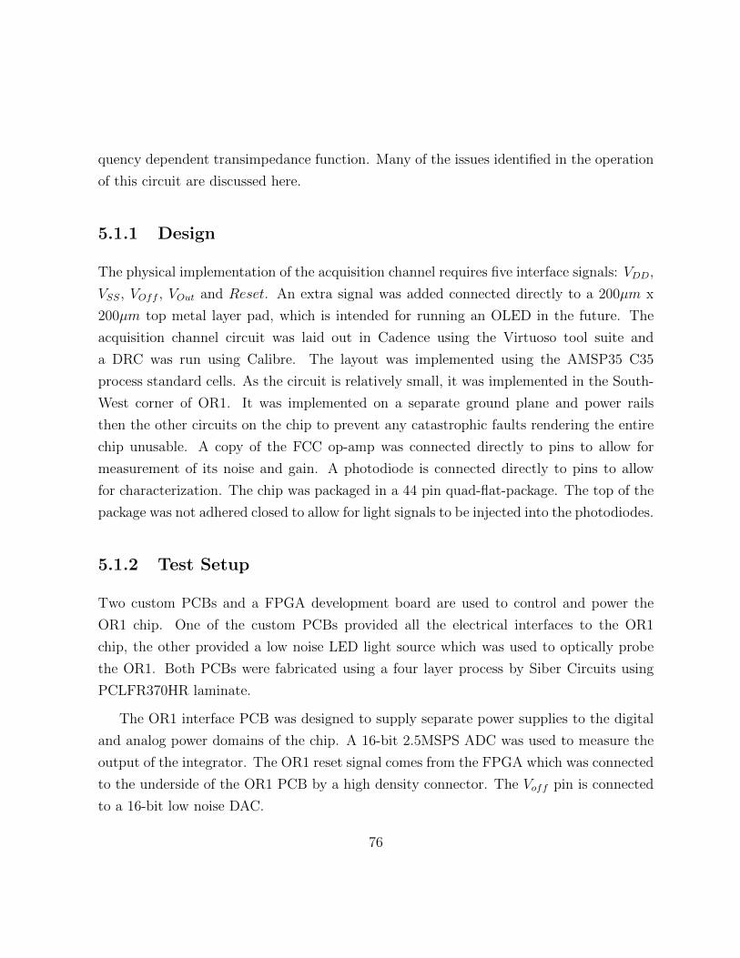
quency dependent transimpedance function. Many of the issues identified in the operation
of this circuit are discussed here.
5.1.1 Design
The physical implementation of the acquisition channel requires five interface signals: VDD,
VSS, VOff , VOut and Reset. An extra signal was added connected directly to a 200µm x
200µm top metal layer pad, which is intended for running an OLED in the future. The
acquisition channel circuit was laid out in Cadence using the Virtuoso tool suite and
a DRC was run using Calibre. The layout was implemented using the AMSP35 C35
process standard cells. As the circuit is relatively small, it was implemented in the South-
West corner of OR1. It was implemented on a separate ground plane and power rails
then the other circuits on the chip to prevent any catastrophic faults rendering the entire
chip unusable. A copy of the FCC op-amp was connected directly to pins to allow for
measurement of its noise and gain. A photodiode is connected directly to pins to allow
for characterization. The chip was packaged in a 44 pin quad-flat-package. The top of the
package was not adhered closed to allow for light signals to be injected into the photodiodes.
5.1.2 Test Setup
Two custom PCBs and a FPGA development board are used to control and power the
OR1 chip. One of the custom PCBs provided all the electrical interfaces to the OR1
chip, the other provided a low noise LED light source which was used to optically probe
the OR1. Both PCBs were fabricated using a four layer process by Siber Circuits using
PCLFR370HR laminate.
The OR1 interface PCB was designed to supply separate power supplies to the digital
and analog power domains of the chip. A 16-bit 2.5MSPS ADC was used to measure the
output of the integrator. The OR1 reset signal comes from the FPGA which was connected
to the underside of the OR1 PCB by a high density connector. The Voff pin is connected
to a 16-bit low noise DAC.
76
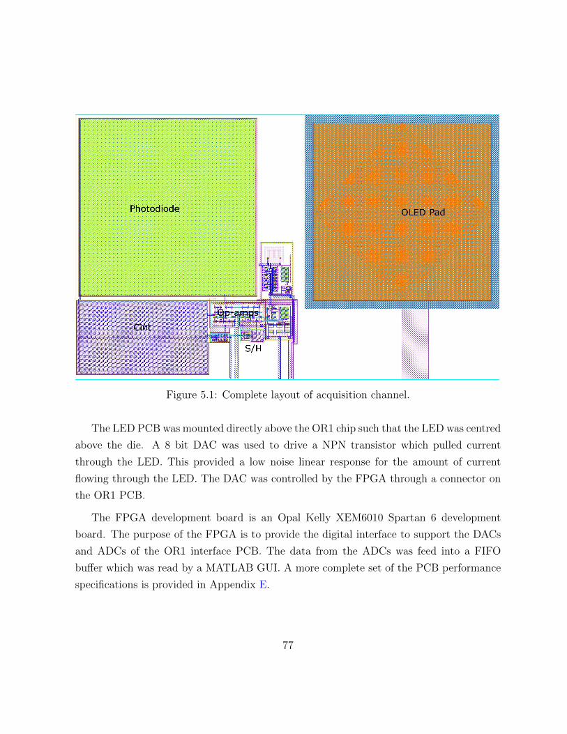
Figure 5.1: Complete layout of acquisition channel.
The LED PCB was mounted directly above the OR1 chip such that the LED was centred
above the die. A 8 bit DAC was used to drive a NPN transistor which pulled current
through the LED. This provided a low noise linear response for the amount of current
flowing through the LED. The DAC was controlled by the FPGA through a connector on
the OR1 PCB.
The FPGA development board is an Opal Kelly XEM6010 Spartan 6 development
board. The purpose of the FPGA is to provide the digital interface to support the DACs
and ADCs of the OR1 interface PCB. The data from the ADCs was feed into a FIFO
buffer which was read by a MATLAB GUI. A more complete set of the PCB performance
specifications is provided in Appendix E.
77
5.1.3 Op-amp Characterization
The FCC op-amp is critical to the performance of the acquisition channel. For this reason a
copy of the FCC op-amp was connected to pins to allow for verification of its performance.
Two of the bias voltages were also connected to pins; both were measured to be less than
1% different from simulation.
To measure the frequency response of the op-amp a common mode voltage of 1.65V was
applied to the inverting terminal of the op-amp. The output of the op-amp balanced mid
rail when the non-inverting terminal was placed at 1.648V. This gives the offset voltage of
the amplifier to be 2mV.
A single frequency tone was then added to one of the rails and the gain was measured.
Initially, the gain was measured to be much lower than expected. It was realized that
due to the large output impedance of the op-amp, the loading placed on the op-amp
by the oscilloscope, compromised the gain. A high input impedance OP129 op-amp was
spliced into the trace in unity feedback to reduce the load current draw. Despite much
effort to remove any residual flux, the parasitic resistance from the solder flux and PCB
substrate, the maximum op-amp gain achieved was AV = 335V/V . This is an order of
magnitude smaller than predicted by simulation. The 3dB frequency was measured to be
f3dB = 1.166kHz. A single pole frequency response was observed. The addition of the
addition of the OP129 buffer did not significantly contribute to the frequency response.
The noise of the op-amp was measured by leaving the op-amp in open loop and record-
ing the output with the ADC. The corner frequency of the noise was found to be 20% higher
than predicted by the unloaded simulation. When the simulation was repeated with load-
ing that results in approximately the same gain, a much better agreement between the
measured and simulated noise was observed (Figure 5.2). The total output referred noise
from the FCC op-amp is measured to be 48.78mVRMS. Input referring the noise PSD gives
a total input referred noise of 1.02mVRMS.
78
101
102
103
104
105
106
10−14
10−12
10−10
10−8
10−6
Frequency [Hz]
Nois
e P
SD
[V
2/H
z]
Opamp Output Noise PSD
Measured
Simulated
Figure 5.2: Comparison between measured and the loaded simulation of the output referrednoise PSD of the FCC op-amp. The slope of the low frequency gain is determined by theflicker noise where as the high frequency slope is determined by the gain roll off of theop-amp. The plateau at the high frequency of the measured results is from the noise floorof the measurement which occurs at 10−13V 2/Hz.
5.1.4 Transient Output
To test the acquisition channel three parameter sweeps are made: vary the light intensity
and measure the integrator output magnitude, vary the integration time and measure the
integrator output, and vary the offset voltage and measure the integrator output. All
measurements of the OR1 integrator output are made using a using Agilent Technologies
MSO-X 3015A oscilloscope. This is because the digital signals used to control the OR1
PCB ADC corrupt the measurement of the signal.
79
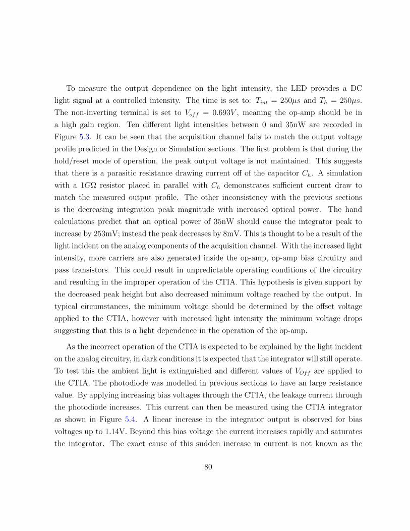
To measure the output dependence on the light intensity, the LED provides a DC
light signal at a controlled intensity. The time is set to: Tint = 250µs and Th = 250µs.
The non-inverting terminal is set to Voff = 0.693V , meaning the op-amp should be in
a high gain region. Ten different light intensities between 0 and 35nW are recorded in
Figure 5.3. It can be seen that the acquisition channel fails to match the output voltage
profile predicted in the Design or Simulation sections. The first problem is that during the
hold/reset mode of operation, the peak output voltage is not maintained. This suggests
that there is a parasitic resistance drawing current off of the capacitor Ch. A simulation
with a 1GΩ resistor placed in parallel with Ch demonstrates sufficient current draw to
match the measured output profile. The other inconsistency with the previous sections
is the decreasing integration peak magnitude with increased optical power. The hand
calculations predict that an optical power of 35nW should cause the integrator peak to
increase by 253mV; instead the peak decreases by 8mV. This is thought to be a result of the
light incident on the analog components of the acquisition channel. With the increased light
intensity, more carriers are also generated inside the op-amp, op-amp bias circuitry and
pass transistors. This could result in unpredictable operating conditions of the circuitry
and resulting in the improper operation of the CTIA. This hypothesis is given support by
the decreased peak height but also decreased minimum voltage reached by the output. In
typical circumstances, the minimum voltage should be determined by the offset voltage
applied to the CTIA, however with increased light intensity the minimum voltage drops
suggesting that this is a light dependence in the operation of the op-amp.
As the incorrect operation of the CTIA is expected to be explained by the light incident
on the analog circuitry, in dark conditions it is expected that the integrator will still operate.
To test this the ambient light is extinguished and different values of VOff are applied to
the CTIA. The photodiode was modelled in previous sections to have an large resistance
value. By applying increasing bias voltages through the CTIA, the leakage current through
the photodiode increases. This current can then be measured using the CTIA integrator
as shown in Figure 5.4. A linear increase in the integrator output is observed for bias
voltages up to 1.14V. Beyond this bias voltage the current increases rapidly and saturates
the integrator. The exact cause of this sudden increase in current is not known as the
80

0 0.1 0.2 0.3 0.4 0.5 0.6 0.7 0.8 0.9 1
x 10−3
0.38
0.385
0.39
0.395
0.4
0.405
0.41
0.415
0.42
Time [s]
Inte
gra
tor
Outp
ut [V
]
IncreasingOpticalPower
(a)
0 5 10 15 20 25 30 35 400.383
0.384
0.385
0.386
0.387
0.388
0.389
0.39
0.391
0.392
Optical Power [nW]
Inte
gra
tion P
eak [V
]
(b)
Figure 5.3: (a) The output of the integrator as a function of time at 10 different opticalpowers on the photodiode. (b) The maximum integrator value for each applied opticalpower.
breakdown voltage of a n well-p sub diode in this process is 24V. Similar results however
are also seen for a discrete photodiode, as will be discussed in Section 5.2.
5.2 Discrete Integrator
Due to problems with the ASIC implementation of the acquisition channel, a circuit similar
to the acquisition channel was implemented using discrete components. The purpose of
the discrete implementation is to demonstrate the transimpedance characteristics of a
CTIA and partially validate the noise calculations derived in Section 3. This section will
outline expected performance of the circuit and give measured results of the noise and
transimpedance characteristics.
5.2.1 Design
The implementation of the discrete CTIA is based around the Texas Instruments IVC102
chip. This is a CTIA with integrated capacitors and reset and hold switches. Used in
81
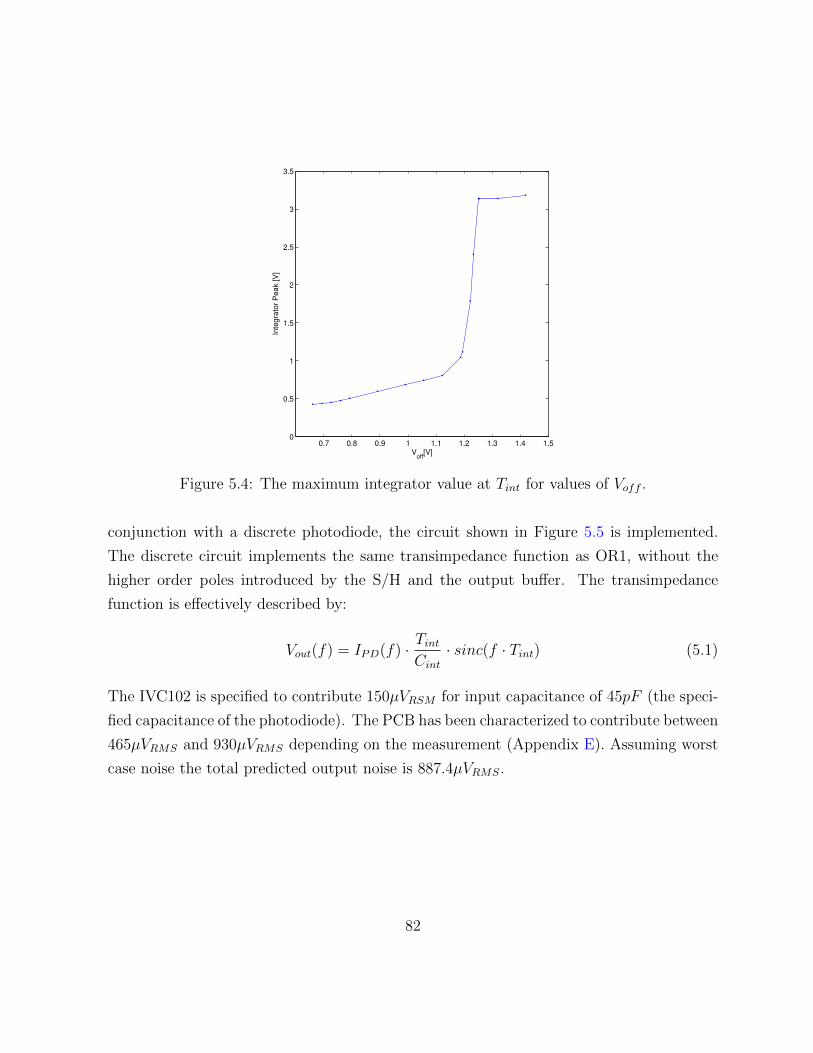
0.7 0.8 0.9 1 1.1 1.2 1.3 1.4 1.50
0.5
1
1.5
2
2.5
3
3.5
Inte
gra
tor
Pe
ak [
V]
Voff
[V]
Figure 5.4: The maximum integrator value at Tint for values of Voff .
conjunction with a discrete photodiode, the circuit shown in Figure 5.5 is implemented.
The discrete circuit implements the same transimpedance function as OR1, without the
higher order poles introduced by the S/H and the output buffer. The transimpedance
function is effectively described by:
Vout(f) = IPD(f) · TintCint· sinc(f · Tint) (5.1)
The IVC102 is specified to contribute 150µVRSM for input capacitance of 45pF (the speci-
fied capacitance of the photodiode). The PCB has been characterized to contribute between
465µVRMS and 930µVRMS depending on the measurement (Appendix E). Assuming worst
case noise the total predicted output noise is 887.4µVRMS.
82
IPD
VPD
φ1
−
+VoffVout
Cint
φ2
(a)
φ1
φ2
VoutTint Th TReset
Ts
(b)
Figure 5.5: (a) The discrete circuit implementation of CTIA. (b) Timing diagram fordiscrete CTIA. Switches φ1 and φ2 are open on logic high.
5.2.2 Test Setup
The discrete integrator circuit is laid out on the same PCB as OR1. The discrete photo-
diode is centred directly below the LED PCB. The Opal Kelly FPGA is used to send the
control signals to the IVC102 integrator chip to match Figure 5.5b. The three phases of
operation are required to ensure that the voltage across the photodiode is reset, otherwise
charge accumulates during the hold period. The MATLAB software written for OR1 can
also control the FPGA timing signals. The same 16 bit 2.5MSPS ADC is used as for the
OR1. For further details on the OR1 PCB refer to Appendix E.
5.2.3 Light Intensity Measurements
The discrete integrator circuit demonstrated the expected output voltage signal profile
with distinct integration, hold and reset phases (Figure 5.6a). When the intensity of the
light was varied, the magnitude of the integrator voltage during the hold stage increased
linearly (Figure 5.6b). The magnitude of the output voltage was higher than predicted
by Eq. 5.1, even when accounting for the tolerance on the integrating capacitor(±20%)
and LED intensities (±15%). This slope would correspond to a capacitance of 6.78pF.
83
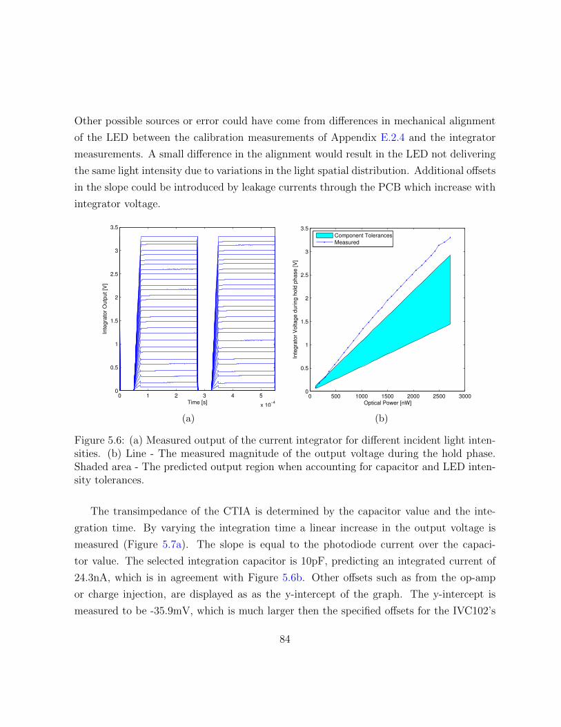
Other possible sources or error could have come from differences in mechanical alignment
of the LED between the calibration measurements of Appendix E.2.4 and the integrator
measurements. A small difference in the alignment would result in the LED not delivering
the same light intensity due to variations in the light spatial distribution. Additional offsets
in the slope could be introduced by leakage currents through the PCB which increase with
integrator voltage.
0 1 2 3 4 5
x 10−4
0
0.5
1
1.5
2
2.5
3
3.5
Time [s]
Inte
gra
tor
Ou
tpu
t [V
]
(a)
0 500 1000 1500 2000 2500 30000
0.5
1
1.5
2
2.5
3
3.5
Optical Power [nW]
Inte
gra
tor
Vo
lta
ge
du
rin
g h
old
ph
ase
[V
]
Component Tolerances
Measured
(b)
Figure 5.6: (a) Measured output of the current integrator for different incident light inten-sities. (b) Line - The measured magnitude of the output voltage during the hold phase.Shaded area - The predicted output region when accounting for capacitor and LED inten-sity tolerances.
The transimpedance of the CTIA is determined by the capacitor value and the inte-
gration time. By varying the integration time a linear increase in the output voltage is
measured (Figure 5.7a). The slope is equal to the photodiode current over the capaci-
tor value. The selected integration capacitor is 10pF, predicting an integrated current of
24.3nA, which is in agreement with Figure 5.6b. Other offsets such as from the op-amp
or charge injection, are displayed as as the y-intercept of the graph. The y-intercept is
measured to be -35.9mV, which is much larger then the specified offsets for the IVC102’s
84
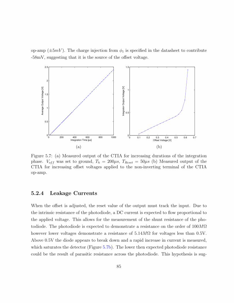
op-amp (±5mV ). The charge injection from φ1 is specified in the datasheet to contribute
-58mV, suggesting that it is the source of the offset voltage.
0 200 400 600 800 10000
0.5
1
1.5
2
2.5
Integration Time [µs]
Ave
rag
e O
utp
ut
Vo
lta
ge
[V
]
(a)
0 0.1 0.2 0.3 0.4 0.5 0.6 0.70
0.5
1
1.5
Offset Voltage [V]
Inte
gra
tor
Ou
tpu
t V
olta
ge
[V
]
(b)
Figure 5.7: (a) Measured output of the CTIA for increasing durations of the integrationphase. Voff was set to ground, Th = 200µs, TReset = 50µs (b) Measured output of theCTIA for increasing offset voltages applied to the non-inverting terminal of the CTIAop-amp.
5.2.4 Leakage Currents
When the offset is adjusted, the reset value of the output must track the input. Due to
the intrinsic resistance of the photodiode, a DC current is expected to flow proportional to
the applied voltage. This allows for the measurement of the shunt resistance of the pho-
todiode. The photodiode is expected to demonstrate a resistance on the order of 100MΩ
however lower voltages demonstrate a resistance of 5.14MΩ for voltages less than 0.5V.
Above 0.5V the diode appears to break down and a rapid increase in current is measured,
which saturates the detector (Figure 5.7b). The lower then expected photodiode resistance
could be the result of parasitic resistance across the photodiode. This hypothesis is sug-
85
gested by initial recordings (not shown) that demonstrated very large currents flowing into
the integrator which were later mitigated by cleaning all the solder points with isopropyl
alcohol to remove residual flux. The sharp increase in the photodiode current is as of yet
unexplained and will need further investigation.
5.2.5 Frequency Response
The frequency response to photodiode currents plays a key role in shaping much of the
noise that propagates through the acquisition channel. The transimpedance of the acqui-
sition channel is measured by sinusoidally modulating the light intensity of the LED and
measuring the magnitude of the output voltage. To do so, the LED drive transistor is feed
a 60mV peak-to-peak sine-wave with a 40mV DC offset by a Agilent 33522A function gen-
erator. An integration period of 50µs is selected to allow for a peak-peak output signal of
2V at low frequencies. The mean of the integrator output is used to calculate the mapping
from the function generator voltage to the photodiode current. The photodiode current
is calculated to have an amplitude of 200nA at low frequencies. Using this, the output
frequency response is predicted to follow Eq. 5.1. The magnitude response is measured as
half the peak-to-peak output voltage of the integrator. Due to digital interference a 40mV
offset is added to the measurement.
Vint(f) = IPD(f) · TintCint· sinc(f · Tint) + 40mV. (5.2)
The magnitude is plotted against the output frequency in Figure 5.8. Close agreement can
be seen between the two plots allowing for the conclusion that Eq. 5.1 accurately predicts
the transimpedance of the acquisition channel.
5.2.6 Output Noise
Despite the difference in circuit architecture, the discrete implementation of the acquisition
channel demonstrates very similar output noise characteristics. Of the four dominant noise
86
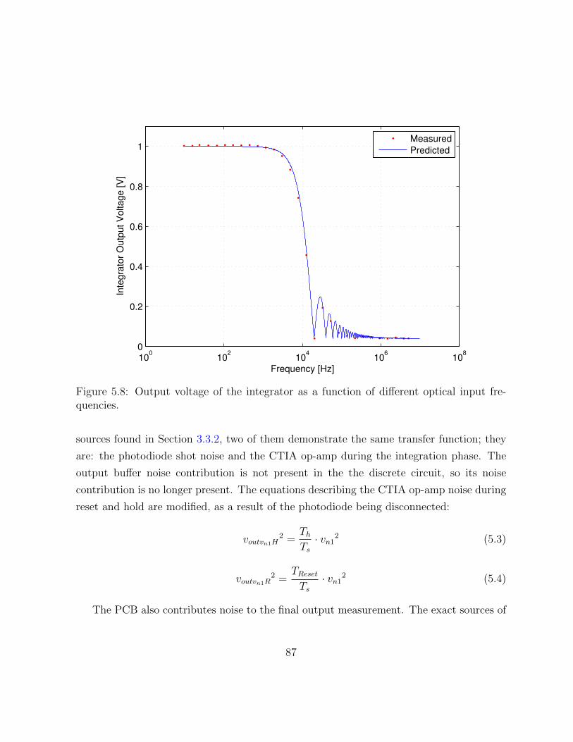
100
102
104
106
108
0
0.2
0.4
0.6
0.8
1
Frequency [Hz]
Inte
gra
tor
Ou
tput V
oltage [V
]
Measured
Predicted
Figure 5.8: Output voltage of the integrator as a function of different optical input fre-quencies.
sources found in Section 3.3.2, two of them demonstrate the same transfer function; they
are: the photodiode shot noise and the CTIA op-amp during the integration phase. The
output buffer noise contribution is not present in the the discrete circuit, so its noise
contribution is no longer present. The equations describing the CTIA op-amp noise during
reset and hold are modified, as a result of the photodiode being disconnected:
voutvn1H2 =
ThTs· vn12 (5.3)
voutvn1R2 =
TResetTs· vn12 (5.4)
The PCB also contributes noise to the final output measurement. The exact sources of
87
this noise is difficult to identify as the PCB contains many possible sources. Characteriza-
tion of the this noise however demonstrated that it is nearly white with an amplitude of
approximately 465µVRMS, depending on the warm-up period of the electronics.
The total noise of the measurement is therefore made up of:
Vn2 = voutinI
2 + voutvn1I2 + voutvn1R
2 + voutvn1H2 + voutPCB
2 (5.5)
=Tint
2 Cint2 · in
2+vn1
2
Ts·(Tint
(1 +
CPDCint
)2
+ Th + TReset
)+ voutPCB
2 (5.6)
As described by Eq. 3.32, the shot noise of the photodiode is related to the incident
light intensity. By increasing the light intensity the output noise should increase. This
is tested in Figure 5.9. The light intensity on the photodiode is increased by increasing
the current driven through the LED above the photodiode. The integration period is
Tint = 10µs, the reset period is TReset = 10µs, and the hold period is Th = 100µs, for a
total period of Ts = 120µs. The photodiode current is calculated by taking the mean value
of the sampled output and dividing by Tint and multiplying by Cint.
The measured noise when the light intensity is increased is slightly higher than that
predicted. The predicted noise is however, based on a calculated value of IPD, which
assumes that the values of Cint and Tint are accurate. The timing is well controlled by the
FPGA, however the value of Cint could be lower than specified by the datasheet. By using
the value of Cint = 6.78pF which was found to fit the data in Figure 5.6b, the predicted
noise follows the measured noise much more accurately. The predicted values assume that
the noise measured when the light is off, is constant while the light intensity increase. The
results shown in Figure 5.9 demonstrates good agreement with the noise predicted by the
equation.
As described by Eq. 5.6, the total noise is also a function of Tint. By increasing
Tint the contribution from the shot noise will increase and the relative contribution from
the CTIA op-amp will be dominated by voutvn1I . This is measured by applying a large
LED intensity onto the photodiode and measuring the standard deviation of the sampled
output for different values of Tint. As the total current can be determined by the mean of
88

0 0.5 1 1.5 2 2.5 3 3.5860
880
900
920
940
960
980
Photodiode Current IPD
[µA]
Measure
d N
ois
e [
µV
RM
S]
Measured, Cint
= 10pF
Calculated, Cint
= 10pF
Measured, Cint
= 6.8pF
Calculated, Cint
= 6.8pF
Figure 5.9: The noise as a function of photodiode photo-current. The measured data backcalculates the photodiode current based on the value of Cint and Tint. The values forCint = 10pF and Cint = 6.8pF are plotted here.
the measured output the total photodiode current for Figure 5.10 is found to be 2.11µA,
taking Cint = 6.8pF as determined before. The op-amp noise vn1 is taken to be 200µVRMS
as specified by the IVC102 datasheet. To calculate the contribution of the noise generated
by the PCB the following equation can be used:
voutPCB2 = Vn
2|Tint=0 − vn12 (5.7)
From this the total noise from the PCB is found to be 218µVRMS.
When the values predicted by Eq. 5.6 for a 50% op-amp noise correlation are compared
to the measured values of the discrete integrator, good agreement is seen for integration
period greater than 2µs . Below 2µs it is suspected that the circuit is still in transi-
89
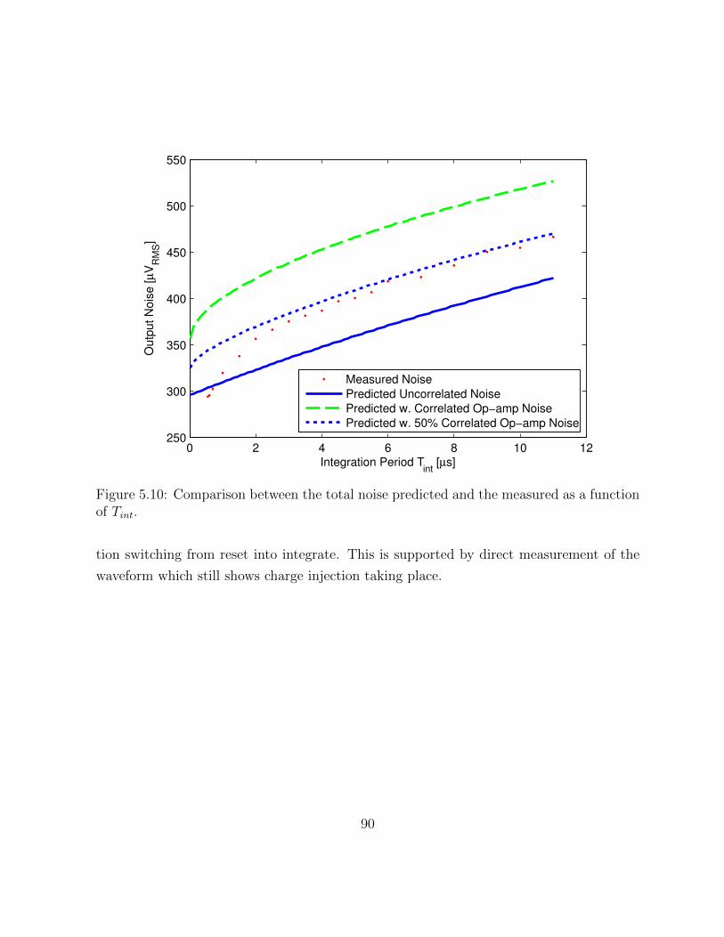
0 2 4 6 8 10 12250
300
350
400
450
500
550
Integration Period Tint
[µs]
Outp
ut N
ois
e [
µV
RM
S]
Measured Noise
Predicted Uncorrelated Noise
Predicted w. Correlated Op−amp Noise
Predicted w. 50% Correlated Op−amp Noise
Figure 5.10: Comparison between the total noise predicted and the measured as a functionof Tint.
tion switching from reset into integrate. This is supported by direct measurement of the
waveform which still shows charge injection taking place.
90
Chapter 6
Discussion and Conclusion
6.1 Discussion of the ASIC Integrator
The physical implementation of the acquisition channel in an ASIC was largely unsuccess-
ful. There were a number of problems which contributed to the failure of this chip including:
the op-amp output resistance; the non-functional S/H circuit; the photo-sensitivity of other
active components of the circuit.
The output buffer was intended to drive off-chip currents to allow for measurement
without compromising the S/H circuit. Simulations of this circuit were performed only
with a probe capacitance and not a parasitic resistance. As the output resistance of the
op-amp is calculated to be approximately 100MΩ, the addition of a probe R = 1MΩ drops
the output resistance and therefore the gain of the op-amp by a factor of 100. When an
ADC is connected to the output, the gain is compromised even further, preventing the
buffer from operating at all.
The S/H circuit was intended to sample the output of the CTIA and hold it for the
output buffer. The measured output profiles of the buffer indicate that after the integra-
tion period the voltage on the hold capacitor begins to droop immediately. Simulations
demonstrate that a parasitic resistance of 1GΩ is sufficient to compromise the performance
91
of the S/H circuit. The circuit extracted from the layout was expected to identify this type
of error, however as shown in Figure 4.4, these simulations demonstrate proper operation.
It is possible that the extraction process was set to ignore parasitics over 1GΩ, which would
result in this being missed.
The photo-sensitivity of the active components of the circuit was an unexpected result.
As the photo-currents generated in the photodiode are on the order of 100nA, the influence
of currents generated in the active components of the circuit were not expected to be
significant in comparison to the currents in the op-amp. However, as the light intensity
increased, the output of the integrator decreased, rendering this circuit useless for optical
detection.
6.2 Discussion of the Discrete Integrator
The implementation of the signal acquisition channel using discrete components demon-
strated far better performance that the ASIC implementation. Possibly the most important
result from the this circuit is the proper demonstration of the CTIA transfer function. Eq.
3.7 demonstrated a close match to the measured results across a wide frequency range.
The discrete implementation however presented several problems intrinsic to discrete
electronics. A significant baseline noise generated by the PCB was measured. This baseline
noise was on the same order of the noise predicted, and fluctuated in time. This compli-
cated the comparison between the noise modelled in Section 3.3.2 and the measurements.
Additionally leakage currents between pins on the ICV102 package resulted in currents
bypassing the input switch and integrating current during the hold phase.
The total noise measured by the discrete implementation of the signal acquisition chan-
nel however mostly followed the trends predicted. As the light intensity was increased, the
shot noise increased as predicted. The noise contributed by the CTIA op-amp however
diverged from the predicted trend. A larger noise amplitude was measured then predicted
by Eq. 5.6, which is hypothesized to be a result of correlated noise. When a 50% cor-
relation was assumed agreement was seen between the modelled noise and the measured
92
results; however, further analysis of this is needed to fully characterise this effect. This
hypothesis is further supported by the transient noise simulation results presented in Fig-
ure 4.13a, which also demonstrate the simulated total noise being higher than expected.
This is despite the transfer function from the non-inverting terminal to the output being
independently validated in Figure 4.8.
6.2.1 Limit of Detection
To calculate the LOD achieved by the discrete integrator a few assumptions can be made
about the signal: (i) the power of the fluorescence signal is described by Eq. 3.2 (ii) the
measured output of the integrator is completely made up of stray excitation light, that is,
the fluorescence is insignificant in comparison.
Using these assumptions the measured data can be used to back calculate the LOD for
the hypothetical LOC device proposed in Section 3. These calculated values are compared
to that predicted by Eq. 3.68, for different values of Tint in Figure 6.1. The trend of the
two lines matches closely, a vertical difference in the values is accounted for by noting that
the op-amp noise in the discrete amplifier was better than that predicted for the CMOS.
From this it can be determined that the minimum LOD for the discrete implementation
of the signal acquisition channel would be 7.2µM .
6.3 Conclusions
This work has performed analysis and measured the noise performance of CTIA-based
circuits for FD in LOC applications. Various relationships were derived for improving the
LOD for CTIA based FD. Some of these relationships were verified in simulation and again
in physical implementation of the proposed signal acquisition channel.
Of the various noise sources identified within the proposed ASIC signal acquisition
channel, three of them dominated over the others. They were: the CTIA op-amp noise,
the photodiode shot noise, and the output buffer noise. Simulations of the output buffer
93
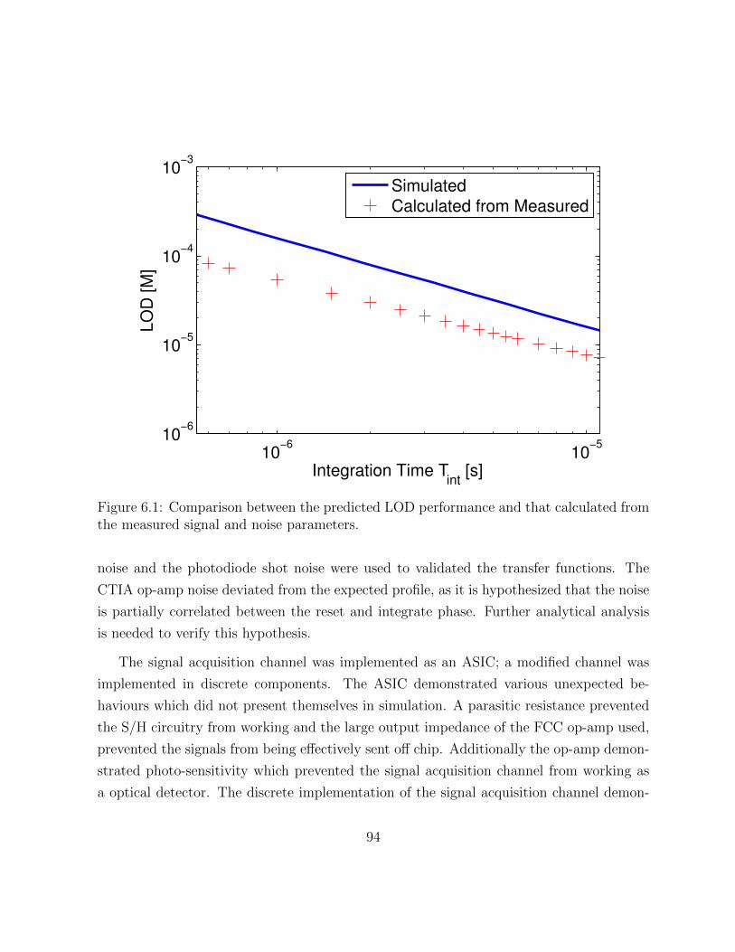
10−6
10−5
10−6
10−5
10−4
10−3
LO
D [M
]
Integration Time Tint
[s]
Simulated
Calculated from Measured
Figure 6.1: Comparison between the predicted LOD performance and that calculated fromthe measured signal and noise parameters.
noise and the photodiode shot noise were used to validated the transfer functions. The
CTIA op-amp noise deviated from the expected profile, as it is hypothesized that the noise
is partially correlated between the reset and integrate phase. Further analytical analysis
is needed to verify this hypothesis.
The signal acquisition channel was implemented as an ASIC; a modified channel was
implemented in discrete components. The ASIC demonstrated various unexpected be-
haviours which did not present themselves in simulation. A parasitic resistance prevented
the S/H circuitry from working and the large output impedance of the FCC op-amp used,
prevented the signals from being effectively sent off chip. Additionally the op-amp demon-
strated photo-sensitivity which prevented the signal acquisition channel from working as
a optical detector. The discrete implementation of the signal acquisition channel demon-
94
strated the trends predicted by simulation and provided validation of the photodiode shot
noise relationship. The discrete implementation demonstrated a SNR which would result
in a LOD of 7.2µM for AF532 fluorophore in the proposed hypothetical LOC FD device.
6.4 Future Directions
There are a number of different directions that this work can be taken. More immediately,
improvements to the signal acquisition channel are proposed. In a broader sense, LOC
FD is a growing field and various options are available. These topics are discussed in the
following sections.
6.4.1 Acquisition Channel
The acquisition channel requires further development before it is ready for integration with
the microfluidics. A working chip must first be demonstrated with the capability to drive
signals off-chip without the assistance of additional buffers. Additionally, a functional
S/H circuit is needed to allow for proper operation of the circuit. Further analysis needs
to be done into the photo-sensitivity of the active components of the circuit. The exact
mechanism for the optical fluctuations needs to be identified so that it can be resolved.
Optically shielding the op-amps and bias-circuitry using a top-metal layer may resolve
many of the issues.
There are various other options for the signal acquisition channel that can also be ex-
plored. It is not necessary to restrict the acquisition channel to integrator based circuits.
Many other groups have started using avalanche photodiodes (APDs) for fluorescence de-
tection applications. These devices effectively have infinite gain making them extremely
sensitive. They also double as ADCs because the photons present themselves as spike
events which can be easily counted by digital circuitry. The problem with APDs is they
require high bias voltages which requires special doping profiles to accommodate, limiting
95
these devices to high voltage CMOS processes. Additionally if photons arrive faster then
the circuit can be clenched, the detector will saturate.
6.4.2 Lab-on-a-Chip Fluorescence Detection
Before a commercially viable LOC FD device is possible there are many engineering chal-
lenges that must be overcome. Much of the rudimentary technologies required for LOC FD
has already been demonstrated. The integrated optics, the fabrication and the electron-
ics have already been demonstrated in isolation. One major challenge which needs to be
overcome is the integration of these many components into a single chip while maintaining
a usable interface. Advanced packaging techniques are needed to allow sample loading,
optical and electrical interfaces to these LOC devices. This is an area of active research
and will likely be seeing significant development in the coming years [63].
Sample preparation has also been identified as an area needing further evaluation. FD
is often only the final step of often long and complicated assays. Much work needs to
be done to automate and integrate these assays into simple preloaded cartridges. The off
chip mixing of reagents is contrary to the model of LOC and reduces the field to only an
incremental improvement to the existing centralized lab model of modern healthcare.
More generally, ASIC based FD, has other applications in other fields of biology. Of
particular interest is opto-genetics, which enables the fluorescence based recording of neu-
ral activity. As it is undesirable to kill the neurological tissue which is being recorded,
integrated implantable devices are being developed for this particular application [64]. To
achieve this, implementation of the excitation light source is needed. Integration of LED
and eventually OLED technology is needed to allow these types of implantable devices.
On chip light sources were discussed in the creation of OR1. Some versions of the chip
have already been integrated with LED dies. Further work is needed to characterize and
model the new excitation schemes possible with this new integrated architecture.
96

Appendices
97
Appendix A
Folded Cascode Op-amp Design
The complete signal acquisition circuit requires two op-amps. The circuit makes use of
an NMOS-input, fully-differential folded cascode (FCC) op-amp previously designed by B.
Crowley in the AMSP350 process. This design is modified from the original, to provide a
single-ended output. Although an FCC op-amp is not ideally suited for this application,
due to its relatively high output impedance, it is used to minimize the number of untested
components used. All biasing circuitry had also been previously taped out and is reused
for this design.
A.1 Gain and Output Impedance
The op-amp schematic is implemented as shown in Figure A.1. Hand calculation of the
gain and output impedance can be performed by analysing the half circuit of the op-amp
(Figure A.2) [61, 65].
The gain (Av) of the op-amp is described by [66]:
Av = GM Rout (A.1)
where Rout is the output impedance of the op-amp and GM is the total transconductance
98
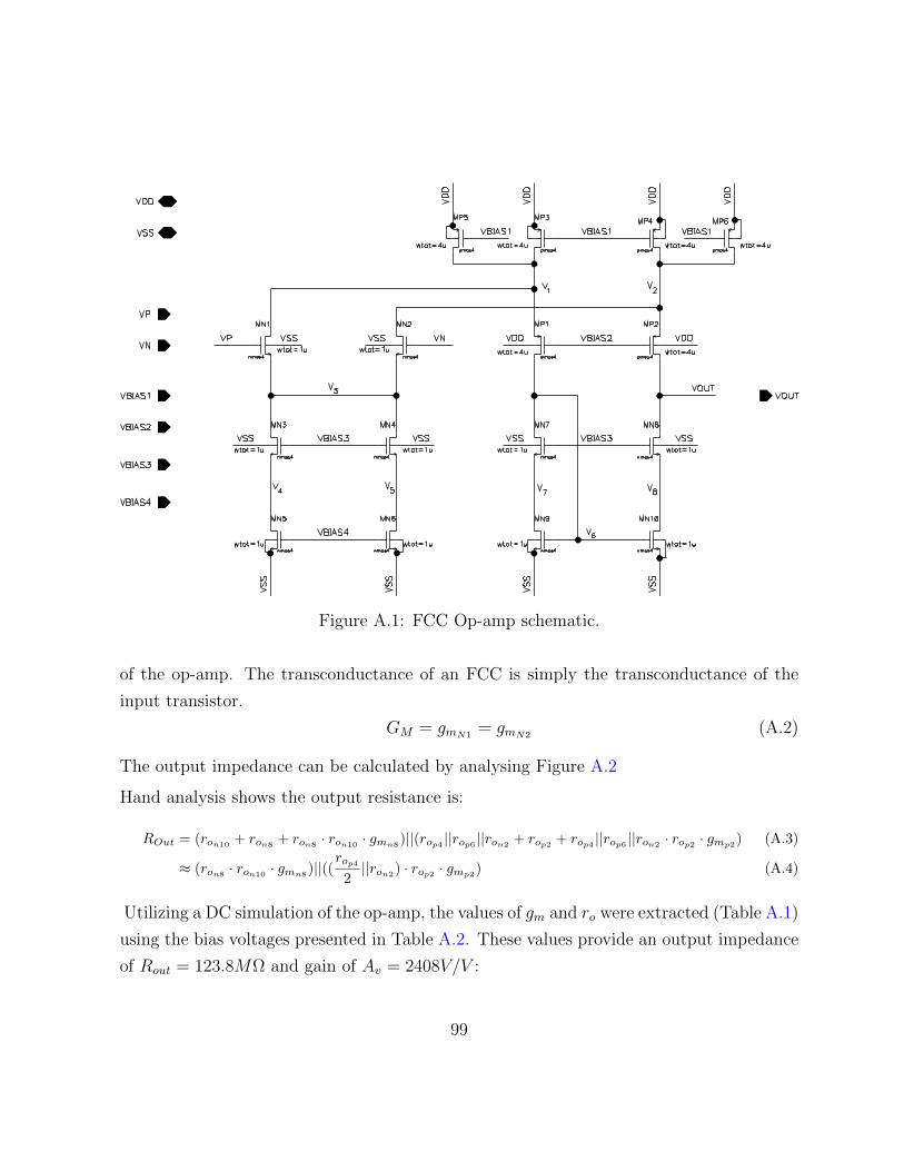
Figure A.1: FCC Op-amp schematic.
of the op-amp. The transconductance of an FCC is simply the transconductance of the
input transistor.
GM = gmN1= gmN2
(A.2)
The output impedance can be calculated by analysing Figure A.2
Hand analysis shows the output resistance is:
ROut = (ron10+ ron8
+ ron8· ron10
· gmn8)||(rop4 ||rop6 ||ron2
+ rop2 + rop4 ||rop6 ||ron2· rop2 · gmp2
) (A.3)
≈ (ron8· ron10
· gmn8)||((rop4
2||ron2
) · rop2 · gmp2) (A.4)
Utilizing a DC simulation of the op-amp, the values of gm and ro were extracted (Table A.1)
using the bias voltages presented in Table A.2. These values provide an output impedance
of Rout = 123.8MΩ and gain of Av = 2408V/V :
99

Figure A.2: Folded Cascode half circuit
Transistor ro[MΩ] gm[µA/V ]MN1 31.358 19.45MN2 31.358 19.45MN3 3.300 18.90MN4 3.300 18.90MN5 10.043 18.89MN6 10.043 18.89MN7 0.782 18.12MN8 0.782 18.12MN9 9.921 18.93MN10 9.921 18.93MP1 15.853 23.46MP2 15.853 23.46MP3 6.105 22.63MP4 6.105 22.63MP5 6.105 22.63MP6 6.105 22.63
Table A.1: Simulated small signal parameters of FCC op-amp transistors. These wereobtained with VCM = 1.65V and bias voltages applied as in Table A.2.
100
VBias [V ]VBias1 2.437VBias2 1.986VBias3 1.303VBias4 0.679
Table A.2: Simulated bias voltages applied to the FCC op-amp.
A.2 Op-amp
The total noise of the op-amp was predicted in hand calculations to contribute 117 µV
of output noise when configured in unity feedback with a 2pF load. Much of these hand
calculations were based off DC operating points extracted from simulations however these
small signal parameters can change depending on the operation of the op-amp. The follow-
ing subsections will validate the hand calculations against Cadence simulations allowing
the hand calculations to be carried forward for use in later parts of the noise analysis of
the fluorescence detection integrator.
A.2.1 Rout and Gm
Based on the hand equations (Equation A.1) provided in the design section, the gain of
the folded cascode op-amp is highly dependent on the values of gm and Rout. Both of
these values depend on the DC operating point of the op-amp. The DC operating points
depend on the biasing, the common mode voltage and the output load. Sweeping the DC
common mode voltage (Figure A.3) allows us to see how linear the gain will be across the
input range. It can be seen that neither Rout or gm provide a good gain for VCM below 0.7
V. This results from the NMOS input stage which isn’t in saturation until VCM is large
enough to drive the current mirror and the NMOS gate. The total gain for different VCM
is shown in Figure A.4.
101
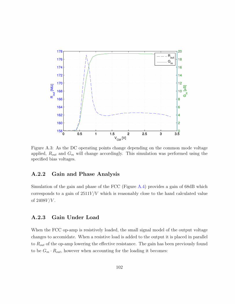
0 0.5 1 1.5 2 2.5 3 3.5158
160
162
164
166
168
170
172
174
176
178
VCM
[V]
Ro
ut [
MΩ
]
0 0.5 1 1.5 2 2.5 3 3.50
2
4
6
8
10
12
14
16
18
20
Gm
[µ
S]
Rout
Gm
Figure A.3: As the DC operating points change depending on the common mode voltageapplied, Rout and Gm will change accordingly. This simulation was performed using thespecified bias voltages.
A.2.2 Gain and Phase Analysis
Simulation of the gain and phase of the FCC (Figure A.4) provides a gain of 68dB which
corresponds to a gain of 2511V/V which is reasonably close to the hand calculated value
of 2408V/V .
A.2.3 Gain Under Load
When the FCC op-amp is resistively loaded, the small signal model of the output voltage
changes to accomidate. When a resistive load is added to the output it is placed in parallel
to Rout of the op-amp lowering the effective resistance. The gain has been previously found
to be Gm ·Rout, however when accounting for the loading it becomes:
102

100
102
104
106
108
01020304050607080
VCM
= 1.65 V
Frequency [Hz]
Ga
in [
dB
v]
0 0.5 1 1.5 2 2.5 3 3.5−100
−50
0
50
100
VCM
[V]
Ga
in [
dB
v]
100
102
104
106
108020406080100120140160
Ph
ase
[D
eg
ree
s]
Gain
Phase
Figure A.4: Top: Gain and Phase of the folded cascode op-amp unloaded. Maximum gainis 69.8 dBv. Bottom: Gain as calculated by multiplying extracted gm and Rout values.Maximum gain is around 70.0 dBv.
Av = Gm · (Rout||RLoad) (A.5)
Thus as the load impedance decreases the gain also decreases (Figure A.5). The load
will also effect the DC operating points of the cascoded transistors further effecting the
gain. Conventionally this wouldn’t dramatically influence the gain as Rout is usually smaller
than RLoad but because of the high output impedance, even negligible loading (i.e. parasitic
resistance of the PCB) will dramatically reduce the gain.
A.2.4 Noise Performance
To initially verify the matrix of equations (Section A.3.1) used to solve for the tran-
simpedance for each transistors noise, the AC node voltages were also calculated using
103

106
107
108
109
1010
1011
1012
10
20
30
40
50
60
70A
v [dB
v]
RLoad
[Ω]
Simulated
Theoretical
Figure A.5: As the output load is increased the gain at a common mode input voltage of1.65V increases until it plateaus. In the hand calculated model (Eq. A.5) the gain managesto plateau around 400MΩ however in the simulation the plateau doesn’t occur until muchhigher load impedances around 10GΩ.
the DC operating points presented in Table A.1. As can be seen in Table A.3 the equation
matrix provides a fairly close approximation to the node voltages predicted by the spectre
models.
As shown in Table A.4 the hand calculated noise for each transistor provides a fairly
accurate value for the noise contributed. It can be seen that the lower frequency hand
calculation is less accurate then the high frequency. It is suspected that this is because
in the AMS documentation they provide two sets of equations for flicker noise, which
is dominant at lower frequencies. One equation provides all the parameters but is less
accurate, the other involves term representing a non-linear expression not given in the
documentation. This was also observed in Appendix C.
104
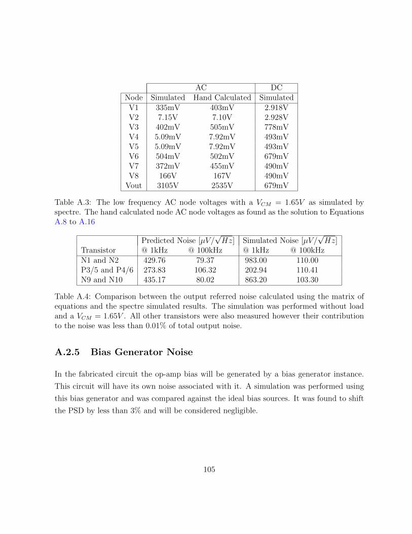
AC DCNode Simulated Hand Calculated SimulatedV1 335mV 403mV 2.918VV2 7.15V 7.10V 2.928VV3 402mV 505mV 778mVV4 5.09mV 7.92mV 493mVV5 5.09mV 7.92mV 493mVV6 504mV 502mV 679mVV7 372mV 455mV 490mVV8 166V 167V 490mV
Vout 3105V 2535V 679mV
Table A.3: The low frequency AC node voltages with a VCM = 1.65V as simulated byspectre. The hand calculated node AC node voltages as found as the solution to EquationsA.8 to A.16
Predicted Noise [µV/√Hz] Simulated Noise [µV/
√Hz]
Transistor @ 1kHz @ 100kHz @ 1kHz @ 100kHzN1 and N2 429.76 79.37 983.00 110.00P3/5 and P4/6 273.83 106.32 202.94 110.41N9 and N10 435.17 80.02 863.20 103.30
Table A.4: Comparison between the output referred noise calculated using the matrix ofequations and the spectre simulated results. The simulation was performed without loadand a VCM = 1.65V . All other transistors were also measured however their contributionto the noise was less than 0.01% of total output noise.
A.2.5 Bias Generator Noise
In the fabricated circuit the op-amp bias will be generated by a bias generator instance.
This circuit will have its own noise associated with it. A simulation was performed using
this bias generator and was compared against the ideal bias sources. It was found to shift
the PSD by less than 3% and will be considered negligible.
105
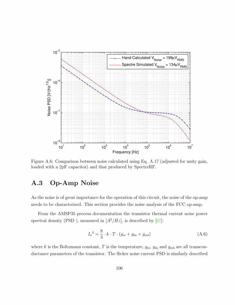
101
102
103
104
105
106
107
10−8
10−7
10−6
10−5
Frequency [Hz]
Nois
e P
SD
[V
/(H
z1/2
)]
Hand Calculated VNoise
= 199µVRMS
Spectre Simulated VNoise
= 134µVRMS
Figure A.6: Comparison between noise calculated using Eq. A.17 (adjusted for unity gain,loaded with a 2pF capacitor) and that produced by SpectreRF.
A.3 Op-Amp Noise
As the noise is of great importance for the operation of this circuit, the noise of the op-amp
needs to be characterized. This section provides the noise analysis of the FCC op-amp.
From the AMSP35 process documentation the transistor thermal current noise power
spectral density (PSD ), measured in [A2/Hz], is described by [67]:
In2 =
8
3· k · T · (gm + gds + gmb) (A.6)
where k is the Boltzmann constant, T is the temperature, gm, gds and gmb are all transcon-
ductance parameters of the transistor. The flicker noise current PSD is similarly described
106
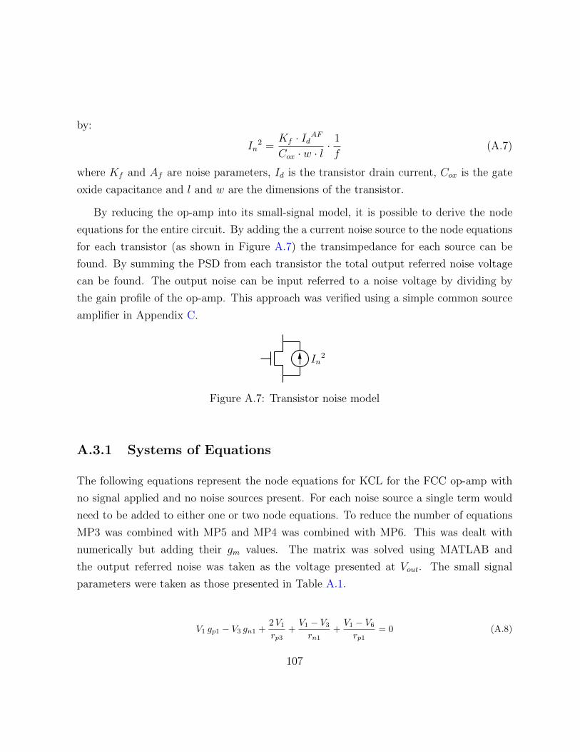
by:
In2 =
Kf · IdAFCox · w · l
· 1
f(A.7)
where Kf and Af are noise parameters, Id is the transistor drain current, Cox is the gate
oxide capacitance and l and w are the dimensions of the transistor.
By reducing the op-amp into its small-signal model, it is possible to derive the node
equations for the entire circuit. By adding the a current noise source to the node equations
for each transistor (as shown in Figure A.7) the transimpedance for each source can be
found. By summing the PSD from each transistor the total output referred noise voltage
can be found. The output noise can be input referred to a noise voltage by dividing by
the gain profile of the op-amp. This approach was verified using a simple common source
amplifier in Appendix C.
In2
Figure A.7: Transistor noise model
A.3.1 Systems of Equations
The following equations represent the node equations for KCL for the FCC op-amp with
no signal applied and no noise sources present. For each noise source a single term would
need to be added to either one or two node equations. To reduce the number of equations
MP3 was combined with MP5 and MP4 was combined with MP6. This was dealt with
numerically but adding their gm values. The matrix was solved using MATLAB and
the output referred noise was taken as the voltage presented at Vout. The small signal
parameters were taken as those presented in Table A.1.
V1 gp1 − V3 gn1 +2V1rp3
+V1 − V3rn1
+V1 − V6rp1
= 0 (A.8)
107
V2 gp2 − V3 gn2 +2V2rp4
+V2 − V3rn2
+V2 − Vout
rp2= 0 (A.9)
V1 − V3rn1
− V3 gn2 − V3 gn1 +V2 − V3rn2
=V3 − V4rn3
− V5 gn4 − V4 gn3 +V3 − V5rn4
(A.10)
V3 − V4rn3
− V4 gn3 =V4rn5
(A.11)
V3 − V5rn4
− V5 gn4 =V5rn6
(A.12)
V1 gp1 +V1 − V6rp1
=V6 − V7rn7
− V7 gn7 (A.13)
V6 − V7rn7
− V7 gn7 = V6 gn9 +V7rn9
(A.14)
− V8 gn8 −V8 − Vout
rn8= V6 gn10 +
V8rn10
(A.15)
V2 gp2 +V2 − Vout
rp2= −V8 gn8 −
V8 − Voutrn8
(A.16)
A.3.2 Noise Transimpedance
By solving for the transimpedance from the transistor to the output seen by each noise
current source, the output-referred noise voltage can be calculated. Examining Table A.5,
it can be seen that only six transistors contribute significantly to the output noise. These
transistors are also mirrored in each half circuit. By examining the half circuit small
signal models it can be seen that MN2, MP4/6 and MN10 (and the mirrored counter parts
MN1, MP3/5 and MN9) all see the output impedance of the op-amp providing the largest
amplification of the noise. All the other transistors see significantly lower impedances thus
making their noise contributions negligible.
This allows for the total output referred noise contributed to be summarized into a
reduced equation:
VNout
2 = 2 ·Rout2 · (InN2
2 + InN10
2 + 2 · InP4
2) (A.17)
108
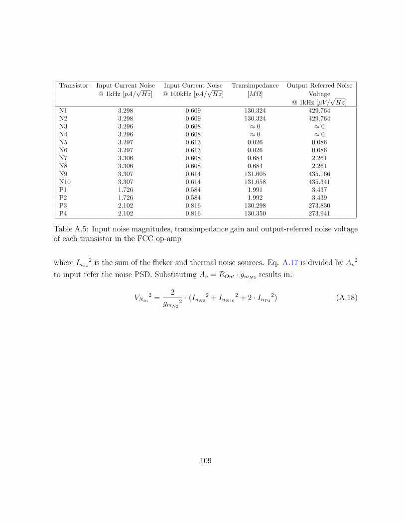
Transistor Input Current Noise Input Current Noise Transimpedance Output Referred Noise
@ 1kHz [pA/√Hz] @ 100kHz [pA/
√Hz] [MΩ] Voltage
@ 1kHz [µV/√Hz]
N1 3.298 0.609 130.324 429.764N2 3.298 0.609 130.324 429.764N3 3.296 0.608 ≈ 0 ≈ 0N4 3.296 0.608 ≈ 0 ≈ 0N5 3.297 0.613 0.026 0.086N6 3.297 0.613 0.026 0.086N7 3.306 0.608 0.684 2.261N8 3.306 0.608 0.684 2.261N9 3.307 0.614 131.605 435.166N10 3.307 0.614 131.658 435.341P1 1.726 0.584 1.991 3.437P2 1.726 0.584 1.992 3.439P3 2.102 0.816 130.298 273.830P4 2.102 0.816 130.350 273.941
Table A.5: Input noise magnitudes, transimpedance gain and output-referred noise voltageof each transistor in the FCC op-amp
where Inxx
2 is the sum of the flicker and thermal noise sources. Eq. A.17 is divided by Av2
to input refer the noise PSD. Substituting Av = ROut · gmN2results in:
VNin
2 =2
gmN22· (InN2
2 + InN10
2 + 2 · InP4
2) (A.18)
109
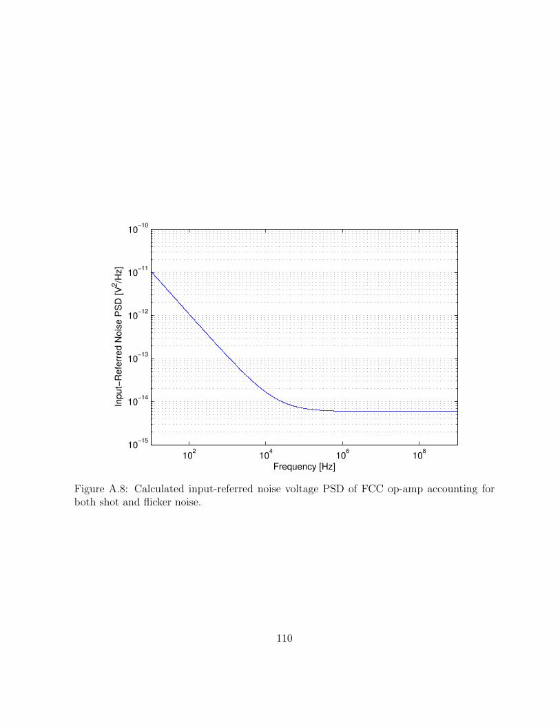
102
104
106
108
10−15
10−14
10−13
10−12
10−11
10−10
Input−
Refe
rred N
ois
e P
SD
[V
2/H
z]
Frequency [Hz]
Figure A.8: Calculated input-referred noise voltage PSD of FCC op-amp accounting forboth shot and flicker noise.
110
Appendix B
LED Power Calculations
B.1 LED Power Calculations
To convert from lumens or candelas to watts is not a straight forward calculation. Lumens
are mapped to the responsivity of the human eye and thus green LEDs are more lumeniant
that blue or red LEDs.
Lumens are roughly the equivalent of total power emitted by a source. Candelas can be
though of as an angular power density. As we are operating in three dimensions steradians
are used instead of radians.
To get the candela for an LED you simply divide the lumenous intensity by the solid
viewing angle of the LED.
Iv[cd] =Φv[lm]
Ω[sr](B.1)
To get the solid angle of an LED in steradians, you apply the following equation, where
θ is the viewing angle of the LED.
Ω = 2 ∗ π ∗ (1− cos(θ/2))[sr] (B.2)
111
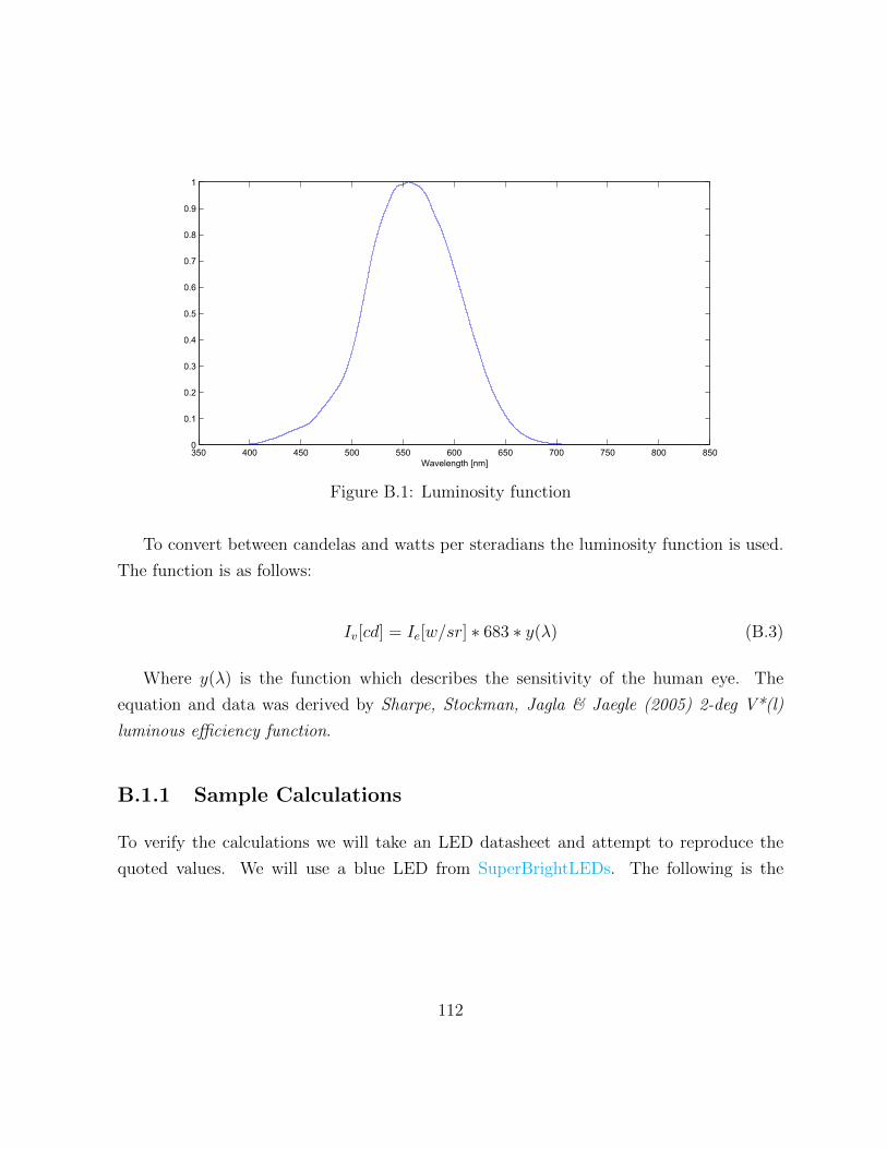
Figure B.1: Luminosity function
To convert between candelas and watts per steradians the luminosity function is used.
The function is as follows:
Iv[cd] = Ie[w/sr] ∗ 683 ∗ y(λ) (B.3)
Where y(λ) is the function which describes the sensitivity of the human eye. The
equation and data was derived by Sharpe, Stockman, Jagla & Jaegle (2005) 2-deg V*(l)
luminous efficiency function.
B.1.1 Sample Calculations
To verify the calculations we will take an LED datasheet and attempt to reproduce the
quoted values. We will use a blue LED from SuperBrightLEDs. The following is the
112

specified values of the LED:
Φv = 0.5lm
θ = 30o
Iv = 2400mcd
λ = 470nm
P = 8.58mW
Can demonstrate the conversion between lumens and millicandelas:
Ω = 2 ∗ π ∗ (1− cos(θ/2))
= 2 ∗ π ∗ (1− cos(30o/2))
= 0.214[sr]
Iv =Ω
Φv
= 0.5/0.214
= 2336mcd
This is within the round off error the specifications.
If we look to convert the lumins to watts, we can use Equation B.3. By cancelling off
the steradians from either side we get:
113
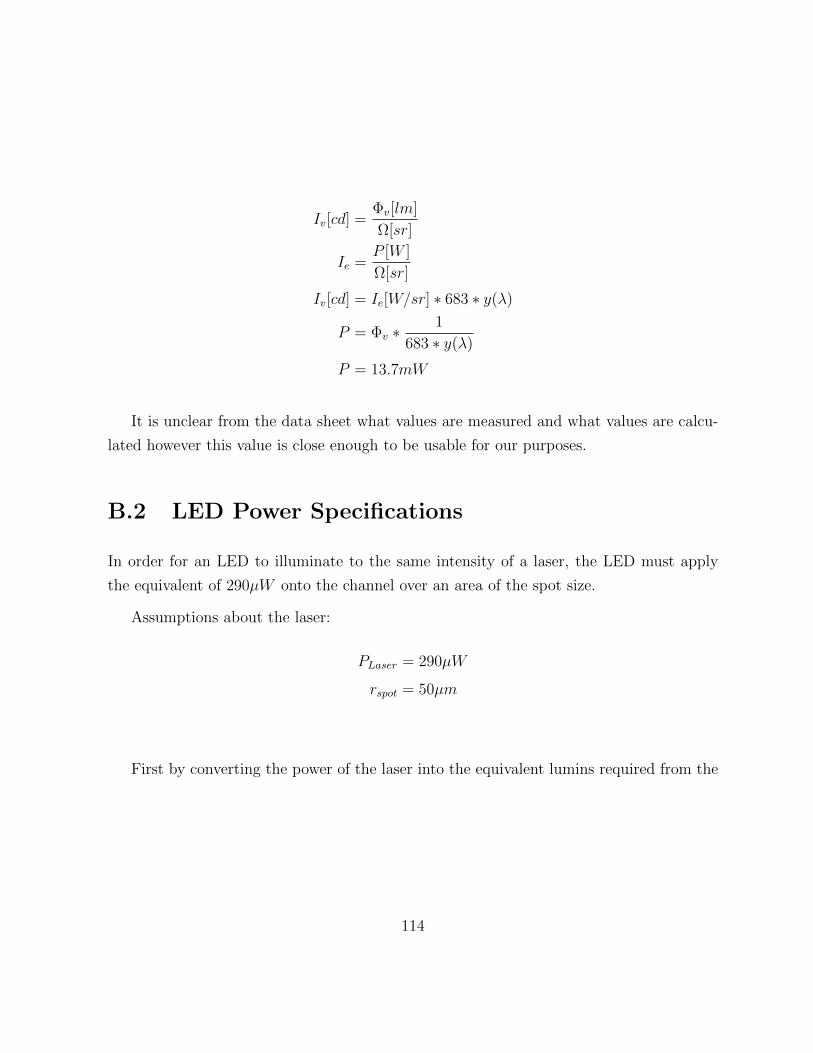
Iv[cd] =Φv[lm]
Ω[sr]
Ie =P [W ]
Ω[sr]
Iv[cd] = Ie[W/sr] ∗ 683 ∗ y(λ)
P = Φv ∗1
683 ∗ y(λ)
P = 13.7mW
It is unclear from the data sheet what values are measured and what values are calcu-
lated however this value is close enough to be usable for our purposes.
B.2 LED Power Specifications
In order for an LED to illuminate to the same intensity of a laser, the LED must apply
the equivalent of 290µW onto the channel over an area of the spot size.
Assumptions about the laser:
PLaser = 290µW
rspot = 50µm
First by converting the power of the laser into the equivalent lumins required from the
114
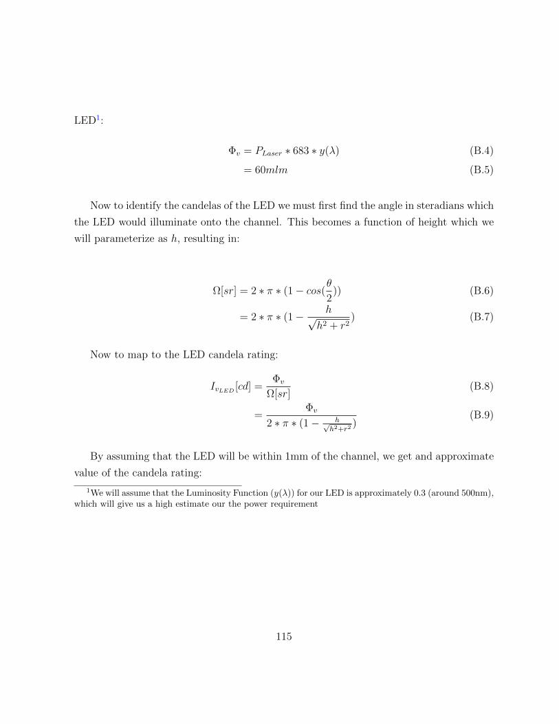
LED1:
Φv = PLaser ∗ 683 ∗ y(λ) (B.4)
= 60mlm (B.5)
Now to identify the candelas of the LED we must first find the angle in steradians which
the LED would illuminate onto the channel. This becomes a function of height which we
will parameterize as h, resulting in:
Ω[sr] = 2 ∗ π ∗ (1− cos(θ2
)) (B.6)
= 2 ∗ π ∗ (1− h√h2 + r2
) (B.7)
Now to map to the LED candela rating:
IvLED[cd] =
Φv
Ω[sr](B.8)
=Φv
2 ∗ π ∗ (1− h√h2+r2
)(B.9)
By assuming that the LED will be within 1mm of the channel, we get and approximate
value of the candela rating:
1We will assume that the Luminosity Function (y(λ)) for our LED is approximately 0.3 (around 500nm),which will give us a high estimate our the power requirement
115

IvLED[cd] =
Φv
2 ∗ π ∗ (1− h√h2+r2
)
=60mcd
2 ∗ π ∗ (1− 1mm√(1mm)2+(50µm)2
)
= 7.6538cd
Thus we require for a LED with a wavelength around 500nm to produce a candela
rating of 7700mcd. A quick search online has identified multiple sources for such LEDs.
However it does appear that such high candela rating does require the larger 5mm diameter
LEDs. Brighter LEDs do exist however these tend to require heat sinks and dramatically
more current, on the order of 700mA-1A, which is beyond our power budget.
Possible suppliers are:
Vendor Part # λ IvLEDPrice [$/each]
SuperBrightLEDs RL5-A7032 507nm 7000mcd $0.54Digikey 754-1607-ND 505nm 12000mcd $0.72Digikey 516-2275-1-ND 470nm 9600mcd $1.45
Table B.1: Possible Suppliers of LEDs for Excitation
B.3 OLED Power Calculations
A typical OLED will quote its optical output in terms of candelas per m2. To convert this
into a power intensity the following conversions must take place:
POLED =AOLED · ρOLED · Ω
683 · y(λ)=
40000µm2 · 1000[cd/m2]1.84[sr]
683 · 1 = 15nW (B.10)
116

Appendix C
Verification of Approach
To test to ensure my methods are accurate, I designed and compared the hand calcula-
tions and simulations of a simple common source amplifier (Figure C.1). The only noise
source in this circuit would be the resistor and nmos transistor. The nmos transistor will
have two sources of noise: Flicker and Thermal. The Thermal noise at low frequencies is
characterized by the following equation taken from the AMS process documentation:
In2 =
8
3· k · T · (gm + gds + gmb) (C.1)
The flicker noise can be similarly characterized by:
In2 =
Kf · IdAFCox · w · l
· 1
f(C.2)
The gain of this amplifier is described by:
Av = gm ∗ (ro||R) (C.3)
117
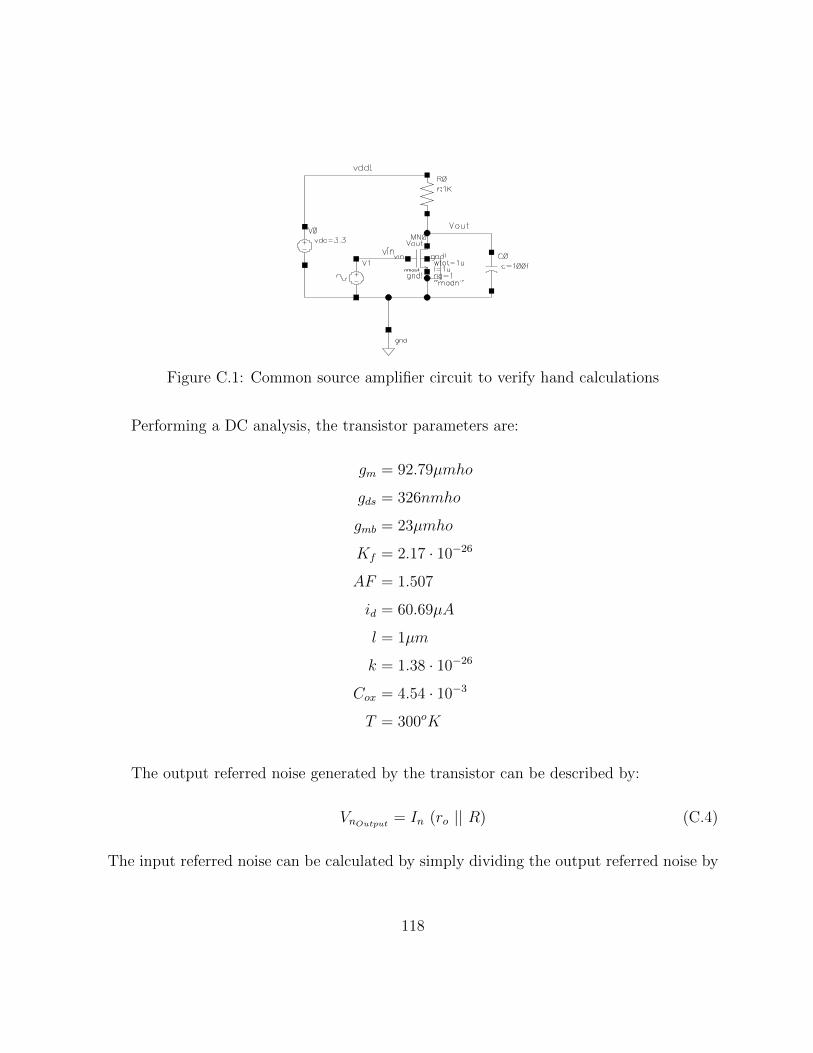
Figure C.1: Common source amplifier circuit to verify hand calculations
Performing a DC analysis, the transistor parameters are:
gm = 92.79µmho
gds = 326nmho
gmb = 23µmho
Kf = 2.17 · 10−26
AF = 1.507
id = 60.69µA
l = 1µm
k = 1.38 · 10−26
Cox = 4.54 · 10−3
T = 300oK
The output referred noise generated by the transistor can be described by:
VnOutput= In (ro || R) (C.4)
The input referred noise can be calculated by simply dividing the output referred noise by
118

Hand Calculated SimulatedReferred Direction Flicker Noise Thermal Noise Flicker Noise Thermal Noise
Output [ V2
Hz ] 2.11 ∗ 10−14 1.28 ∗ 10−18 5.37 ∗ 10−14 1.27 ∗ 10−18
Input [ V2
Hz ] 2.45 ∗ 10−12 1.49 ∗ 10−16 - -
Av 92.8mV/V 92.1mV/V
Table C.1: Results comparison between the hand calculated values and the simulatedvalues.
the gain of the circuit:
VnInput=VnOutput
Av(C.5)
Based off the results shown in Table C.1 it appears that the thermal noise hand calcula-
tions are very close to the expected output referred noise. The flicker noise however doesn’t
seem to present the same level of accuracy. In AMS noise parameter documentation, it is
mentioned that the flicker noise is calculated using a high order function, not provided by
the document. This suggests that the accuracy of the flicker noise hand calculation may
vary dramatically from the simulated value. The gain was nearly perfectly predicted by
the hand calculations.
119
Appendix D
Derivation of CTIA Transimpedance
Function
The transfer function of the CTIA shown in Figure 3.2, is derived by starting with KCL
at the inverting terminal of the op-amp. If we assume that the photodiode can simply be
modelled as a capacitor (CPD) in parallel with a current source (IPD(t)), the node equation
becomes:
IPD(t) + CPD ·dVPDdt
= Cint ·d(Vint − VPD)
dt(D.1)
Using circuit linearity, Voff can be thought of as a ground. Thus the op-amp gain equation
will be:
Vint(s) = A(s)(0− VPD(s)) (D.2)
The circuit will be in this state from t1 = t0 + k · Ts to t2 = t0 + k · Ts + Tint where k ∈ Z.
This allows for the integration to be setup to be:∫ t2
t1
IPD(t)dt+ CPD · VPD(t) = Cint · (Vint(t)− VPD(t)) (D.3)
120
Examining the limits of the integration, this is the equivalent of the indefinite integral of:∫ t2
t1
IPD(t)dt =
∫IPD(t) · [u(t− t1)− u(t− t2)]dt (D.4)
=
∫IPD(t) · [u(t− (t0 + k · Ts))− u(t− (t0 + k · Ts + Tint))]dt (D.5)
Using the definition of convolution of:
f(t) ∗ g(t) ≡∫f(τ) · g(t− τ) · dτ (D.6)
Eq. D.3 becomes:
IPD(t) ∗ [u(t− t1)− u(t− t2)] + CPD · VPD(t) = Cint · (Vint(t)− VPD(t)) (D.7)
Taking Eq. D.7 into the frequency domain:
IPD(s)
s·[e−s·t1 − e−s·t2
]= Cint · (Vint(s)− VPD(s))− CPD · VPD(s) (D.8)
Then by substituting Eq. D.2 into Eq. D.8 and doing some basic manipulation
IPD(s)
s·[e−s·t1 − e−s·t2
]= Vint(s)
(Cint +
CPD + CintA(s)
)(D.9)
The subtracted complex exponentials result in a sine:
e−s·t1 − e−s·t2 = e−s·(t0+k·Ts) − e−s·(t0+k·Ts+Tint)
= e−s·(t0+k·Ts)(1− e−s·Tint)
= e−s·(t0+k·Ts+Tint/2)(es·Tint/2 − e−s·Tint/2)
Then using Euler’s Formula:
sin(x) =ejx − e−jx
2j(D.10)
121
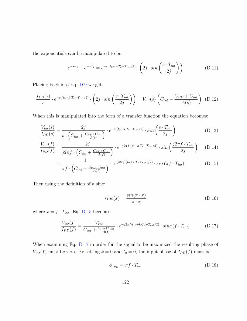
the exponentials can be manipulated to be:
e−s·t1 − e−s·t2 = e−s·(t0+k·Ts+Tint/2) ·(
2j · sin(s · Tint
2j
))(D.11)
Placing back into Eq. D.9 we get:
IPD(s)
s· e−s·(t0+k·Ts+Tint/2) ·
(2j · sin
(s · Tint
2j
))= Vint(s)
(Cint +
CPD + CintA(s)
)(D.12)
When this is manipulated into the form of a transfer function the equation becomes:
Vint(s)
IPD(s)=
2j
s ·(Cint + CPD+Cint
A(s)
) · e−s·(t0+k·Ts+Tint/2) · sin(s · Tint
2j
)(D.13)
Vint(f)
IPD(f)=
2j
j2πf ·(Cint + CPD+Cint
A(f)
) · e−j2πf ·(t0+k·Ts+Tint/2) · sin(j2πf · Tint
2j
)(D.14)
=1
πf ·(Cint + CPD+Cint
A(f)
) · e−j2πf ·(t0+k·Ts+Tint/2) · sin (πf · Tint) (D.15)
Then using the definition of a sinc:
sinc(x) =sin(π · x)
π · x (D.16)
where x = f · Tint. Eq. D.15 becomes:
Vint(f)
IPD(f)=
Tint
Cint + CPD+Cint
A(f)
· e−j2πf ·(t0+k·Ts+Tint/2) · sinc (f · Tint) (D.17)
When examining Eq. D.17 in order for the signal to be maximized the resulting phase of
Vint(f) must be zero. By setting k = 0 and t0 = 0, the input phase of IPD(f) must be:
φIPD= πf · Tint (D.18)
122
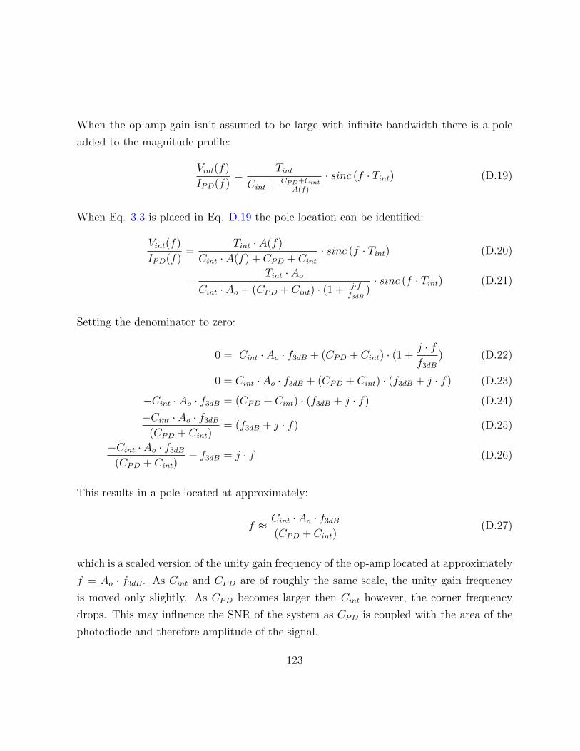
When the op-amp gain isn’t assumed to be large with infinite bandwidth there is a pole
added to the magnitude profile:
Vint(f)
IPD(f)=
Tint
Cint + CPD+Cint
A(f)
· sinc (f · Tint) (D.19)
When Eq. 3.3 is placed in Eq. D.19 the pole location can be identified:
Vint(f)
IPD(f)=
Tint · A(f)
Cint · A(f) + CPD + Cint· sinc (f · Tint) (D.20)
=Tint · Ao
Cint · Ao + (CPD + Cint) · (1 + j·ff3dB
)· sinc (f · Tint) (D.21)
Setting the denominator to zero:
0 = Cint · Ao · f3dB + (CPD + Cint) · (1 +j · ff3dB
) (D.22)
0 = Cint · Ao · f3dB + (CPD + Cint) · (f3dB + j · f) (D.23)
−Cint · Ao · f3dB = (CPD + Cint) · (f3dB + j · f) (D.24)
−Cint · Ao · f3dB(CPD + Cint)
= (f3dB + j · f) (D.25)
−Cint · Ao · f3dB(CPD + Cint)
− f3dB = j · f (D.26)
This results in a pole located at approximately:
f ≈ Cint · Ao · f3dB(CPD + Cint)
(D.27)
which is a scaled version of the unity gain frequency of the op-amp located at approximately
f = Ao · f3dB. As Cint and CPD are of roughly the same scale, the unity gain frequency
is moved only slightly. As CPD becomes larger then Cint however, the corner frequency
drops. This may influence the SNR of the system as CPD is coupled with the area of the
photodiode and therefore amplitude of the signal.
123

As is described by Xu and Yuan [68], the 3dB frequency of the sinc function is located
at 0.44/Tint. Assuming that:0.44
Tint Cint · Ao · f3dB
(CPD + Cint)(D.28)
the higher order pole does not significantly influence the result. Thus, A(f) can be assumed
to be large for all frequencies.
To look strictly at the magnitude response the phase modifying term can be dropped.
By doing so Eq. D.17 comes back to the common form of integrator equation:∥∥∥∥Vint(f)
IPD(f)
∥∥∥∥ =
∥∥∥∥TintCint· sinc (f · Tint)
∥∥∥∥ (D.29)
124

Appendix E
OR1 PCB Datasheet
E.1 PCB Design
A Printed Circuit Board (PCB) was designed for the purpose of testing and verification
of the OR1 chip. The control signalling and USB interface was provided through an Opal
Kelly XEM6010-LX45 FPGA board which attached to the bottom of the OR1 Board.
E.2 PCB Calibration
E.2.1 Measuring ADC SNR
To measure the SNR of the ADC the standard practice is to apply a sine wave and measure
the take the FFT of the recorded signal. The sine wave needs to be of a frequency such
that its frequency is a integer multiple of the bin frequency of the recording. Additionally,
the number of samples needs to be a value of 2n, where n is a positive integer. [69]
125
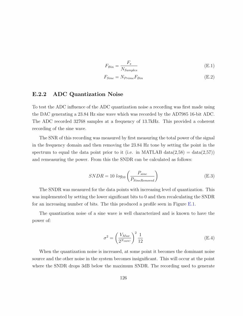
FBin =Fs
NSamples
(E.1)
FSine = NPrimeFBin (E.2)
E.2.2 ADC Quantization Noise
To test the ADC influence of the ADC quantization noise a recording was first made using
the DAC generating a 23.84 Hz sine wave which was recorded by the AD7985 16-bit ADC.
The ADC recorded 32768 samples at a frequency of 13.7kHz. This provided a coherent
recording of the sine wave.
The SNR of this recording was measured by first measuring the total power of the signal
in the frequency domain and then removing the 23.84 Hz tone by setting the point in the
spectrum to equal the data point prior to it (i.e. in MATLAB data(2,58) = data(2,57))
and remeasuring the power. From this the SNDR can be calculated as follows:
SNDR = 10 log10
(Psine
PSineRemoved
)(E.3)
The SNDR was measured for the data points with increasing level of quantization. This
was implemented by setting the lower significant bits to 0 and then recalculating the SNDR
for an increasing number of bits. The this produced a profile seen in Figure E.1.
The quantization noise of a sine wave is well characterized and is known to have the
power of:
σ2 =
(VMax
2NADC
)21
12(E.4)
When the quantization noise is increased, at some point it becomes the dominant noise
source and the other noise in the system becomes insignificant. This will occur at the point
where the SNDR drops 3dB below the maximum SNDR. The recording used to generate
126

02468101214160
10
20
30
40
50
60
70
Number of Bits NADC
SN
DR
[dB
v]
Figure E.1: SNR vs Quantized ADC values
127
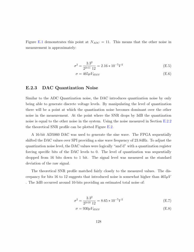
Figure E.1 demonstrates this point at NADC = 11. This means that the other noise in
measurement is approximately:
σ2 =3.32
22∗11 12= 2.16 ∗ 10−7V 2 (E.5)
σ = 465µVRMS (E.6)
E.2.3 DAC Quantization Noise
Similar to the ADC Quantization noise, the DAC introduces quantization noise by only
being able to generate discrete voltage levels. By manipulating the level of quantization
there will be a point at which the quantization noise becomes dominant over the other
noise in the measurement. At the point where the SNR drops by 3dB the quantization
noise is equal to the other noise in the system. Using the noise measured in Section E.2.2
the theoretical SNR profile can be plotted Figure E.2.
A 16-bit AD5060 DAC was used to generate the sine wave. The FPGA sequentially
shifted the DAC values over SPI providing a sine wave frequency of 23.84Hz. To adjust the
quantization noise level, the DAC values were logically “and’d” with a quantization register
forcing specific bits of the DAC levels to 0. The level of quantization was sequentially
dropped from 16 bits down to 1 bit. The signal level was measured as the standard
deviation of the raw signal.
The theoretical SNR profile matched fairly closely to the measured values. The dis-
crepancy for bits 16 to 12 suggests that introduced noise is somewhat higher than 465µV
. The 3dB occurred around 10-bits providing an estimated total noise of:
σ2 =3.32
22∗10 12= 8.65 ∗ 10−7V 2 (E.7)
σ = 930µVRMS (E.8)
128
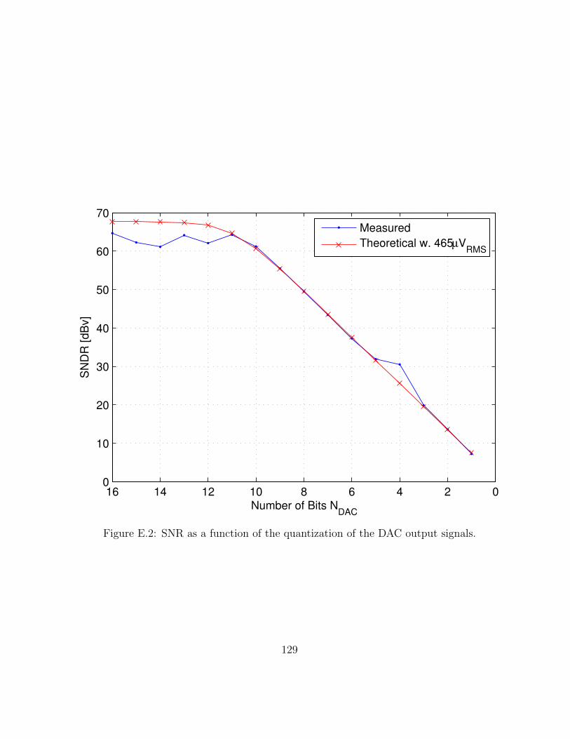
02468101214160
10
20
30
40
50
60
70
Number of Bits NDAC
SN
DR
[d
Bv]
Measured
Theoretical w. 465µVRMS
Figure E.2: SNR as a function of the quantization of the DAC output signals.
129
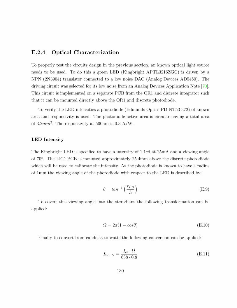
E.2.4 Optical Characterization
To properly test the circuits design in the previous section, an known optical light source
needs to be used. To do this a green LED (Kingbright APTL3216ZGC) is driven by a
NPN (2N3904) transistor connected to a low noise DAC (Analog Devices AD5450). The
driving circuit was selected for its low noise from an Analog Devices Application Note [70].
This circuit is implemented on a separate PCB from the OR1 and discrete integrator such
that it can be mounted directly above the OR1 and discrete photodiode.
To verify the LED intensities a photodiode (Edmunds Optics PD-NT53 372) of known
area and responsivity is used. The photodiode active area is circular having a total area
of 3.2mm2. The responsivity at 500nm is 0.3 A/W.
LED Intensity
The Kingbright LED is specified to have a intensity of 1.1cd at 25mA and a viewing angle
of 70o. The LED PCB is mounted approximately 25.4mm above the discrete photodiode
which will be used to calibrate the intensity. As the photodiode is known to have a radius
of 1mm the viewing angle of the photodiode with respect to the LED is described by:
θ = tan−1(rPDh
)(E.9)
To covert this viewing angle into the steradians the following transformation can be
applied:
Ω = 2π(1− cosθ) (E.10)
Finally to convert from candelas to watts the following conversion can be applied:
IWatts =Icd · Ω
638 · 0.8 (E.11)
130
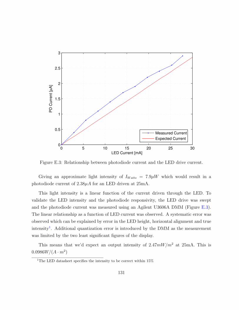
0 5 10 15 20 25 300
0.5
1
1.5
2
2.5
3
LED Current [mA]
PD
Curr
ent [µ
A]
Measured Current
Expected Current
Figure E.3: Relationship between photodiode current and the LED drive current.
Giving an approximate light intensity of IWatts = 7.9µW which would result in a
photodiode current of 2.38µA for an LED driven at 25mA.
This light intensity is a linear function of the current driven through the LED. To
validate the LED intensity and the photodiode responsivity, the LED drive was swept
and the photodiode current was measured using an Agilent U3606A DMM (Figure E.3).
The linear relationship as a function of LED current was observed. A systematic error was
observed which can be explained by error in the LED height, horizontal alignment and true
intensity1. Additional quantization error is introduced by the DMM as the measurement
was limited by the two least significant figures of the display.
This means that we’d expect an output intensity of 2.47mW/m2 at 25mA. This is
0.0986W/(A ·m2)
1The LED datasheet specifies the intensity to be correct within 15%
131

LED Stability
The DAC at max counts output 617 mV. The specified noise value of the drive circuit is
2.42µVRMS [70]. This gives us an expected SNR of 108 dB. This is sufficiently stable that
it is an insignificant source of noise for the photodiode.
E.3 FPGA Memory Map
0: DAC1 EN1: DAC2 EN2:3:4: kTimer Reset OR15: kTimer Reset Discrete Int6: J87: ADC1 Enable8: ADC Sample on End of Integration9: kReset OR1 Force High10: ADC Sample on OR1 Tint else Discrete Tint11: Select Force Reset Signal
12: Force Discrete Reset13: DAC3 Sinewave Mode14: Force Discrete Hold15: DAC1 Sinewave Mode
01234567891011121314150x04
Figure E.4: Memory map of OR1 control register.
132
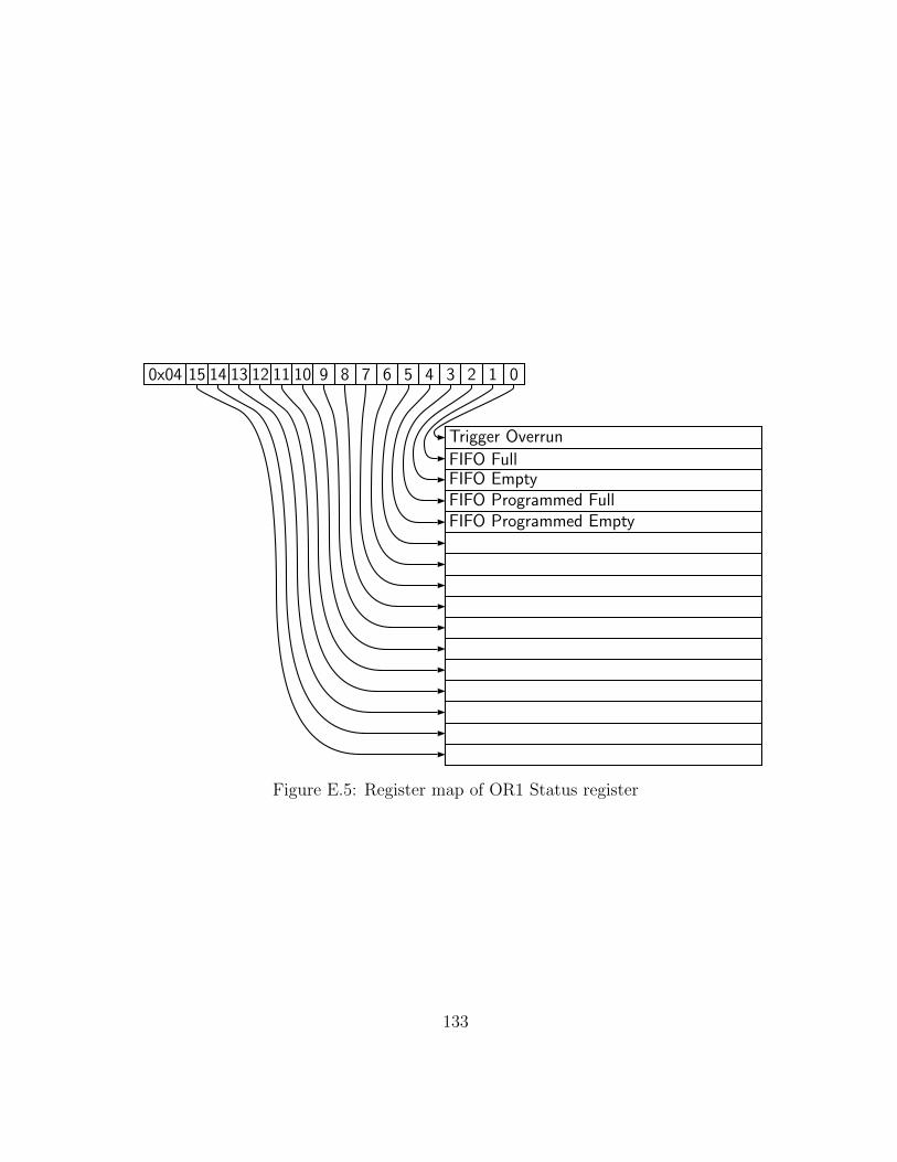
Trigger Overrun
FIFO FullFIFO EmptyFIFO Programmed FullFIFO Programmed Empty
01234567891011121314150x04
Figure E.5: Register map of OR1 Status register
133
Appendix F
Light Collection Efficiency
Calculation
Integration of a photodiode into a microfluidic chip is thought to increase the sensitivity
of the optical detection of fluorescence. The idea is that as proximity of the photodiode
increases, no collection optics will be required to direct the light onto the photodiode.
F.1 Derivation
The nature of an isotropic light source dictates that the power emitted from the source
will be distributed over the total area of a sphere with the point source at the centre.
Beginning with the total surface area of a sphere:
SA = 4πr2 (F.1)
This can be used to identify the total intensity of light on the surface of the sphere:
I =PtotalSA
=Ptotal4πr2
(F.2)
134
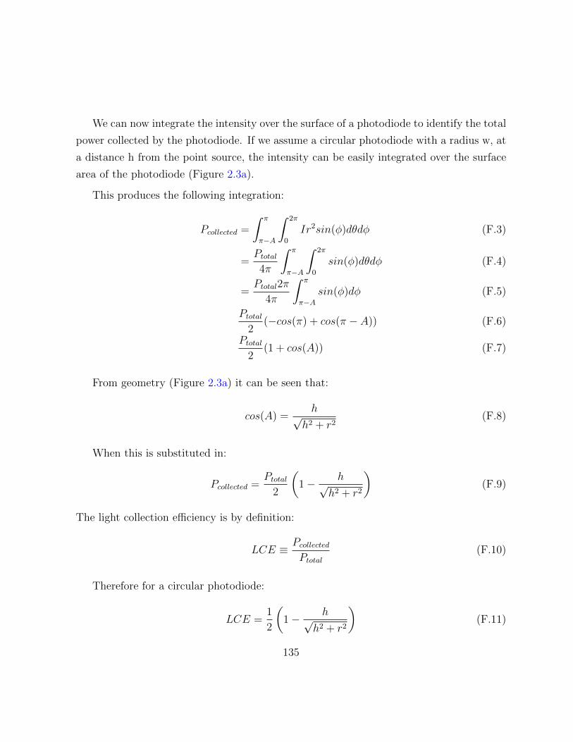
We can now integrate the intensity over the surface of a photodiode to identify the total
power collected by the photodiode. If we assume a circular photodiode with a radius w, at
a distance h from the point source, the intensity can be easily integrated over the surface
area of the photodiode (Figure 2.3a).
This produces the following integration:
Pcollected =
∫ π
π−A
∫ 2π
0
Ir2sin(φ)dθdφ (F.3)
=Ptotal4π
∫ π
π−A
∫ 2π
0
sin(φ)dθdφ (F.4)
=Ptotal2π
4π
∫ π
π−Asin(φ)dφ (F.5)
Ptotal2
(−cos(π) + cos(π − A)) (F.6)
Ptotal2
(1 + cos(A)) (F.7)
From geometry (Figure 2.3a) it can be seen that:
cos(A) =h√
h2 + r2(F.8)
When this is substituted in:
Pcollected =Ptotal
2
(1− h√
h2 + r2
)(F.9)
The light collection efficiency is by definition:
LCE ≡ PcollectedPtotal
(F.10)
Therefore for a circular photodiode:
LCE =1
2
(1− h√
h2 + r2
)(F.11)
135

F.2 Analysis
This analysis gives a unique perspective on how geometry interplays with the light collection
of isotropic light sources. By plotting the LCE logarithmically with the height of the
isotropic light source, a strong argument can be gained for the advantages of integration.
Figure 3 - LCE of 150?m diameter photodiode When the channel distance to the photo-
diode is approximately the same order of magnitude in size as the distance to the channel,
there is a rapid increase in the light collection efficiency. This shows an interesting number
for our current TTK optics of a LCE of 4%. Alternatively, this same calculation can be
used for sizing of a photodiode for a given process. Current estimates from DALSA provide
a separation distance of 20µm. This means that for a LCE of 40% requires a photodiode
with a 200µm diameter.
F.3 Conclusion
Basic geometric analysis has provided a means to size a photodiode based on the distance
from the channel. A rule of thumb is to provide a photodiode which is an order of magnitude
larger than the separation distance. This will provide a large LCE without sacrificing too
much surface area of the wafer.
136
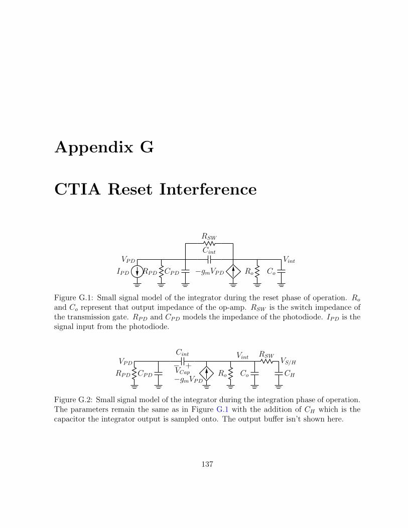
Appendix G
CTIA Reset Interference
IPD
VPD
RPD CPD
Cint
RSW
−gmVPD Ro
Vint
Co
Figure G.1: Small signal model of the integrator during the reset phase of operation. Ro
and Co represent that output impedance of the op-amp. RSW is the switch impedance ofthe transmission gate. RPD and CPD models the impedance of the photodiode. IPD is thesignal input from the photodiode.
VPD
RPD CPD
Cint
−VCap
+
−gmVPDRo
Vint
Co
RSWVS/H
CH
Figure G.2: Small signal model of the integrator during the integration phase of operation.The parameters remain the same as in Figure G.1 with the addition of CH which is thecapacitor the integrator output is sampled onto. The output buffer isn’t shown here.
137
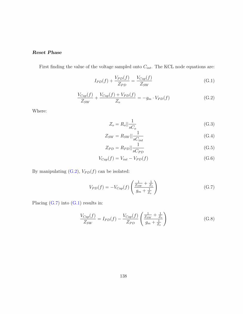
Reset Phase
First finding the value of the voltage sampled onto Cint. The KCL node equations are:
IPD(f) +VPD(f)
ZPD=VCap(f)
ZSW(G.1)
VCap(f)
ZSW+VCap(f) + VPD(f)
Zo= −gm · VPD(f) (G.2)
Where:
Zo = Ro||1
sCo(G.3)
ZSW = RSW ||1
sCint(G.4)
ZPD = RPD||1
sCPD(G.5)
VCap(f) = Vint − VPD(f) (G.6)
By manipulating (G.2), VPD(f) can be isolated:
VPD(f) = −VCap(f)
(1
ZSW+ 1
Zo
gm + 1Zo
)(G.7)
Placing (G.7) into (G.1) results in:
VCap(f)
ZSW= IPD(f)− VCap(f)
ZPD
(1
ZSW+ 1
Zo
gm + 1Zo
)(G.8)
138
which can be manipulated into:
VCap(f)
ZSW+VCap(f)
ZPD
(1
ZSW+ 1
Zo
gm + 1Zo
)= IPD(f) (G.9)
VCap(f)
IPD(f)=
ZSW · ZPD · (gm · Zo ·+1)
Zo · ZPD · gm + Zo + ZPD + ZSW(G.10)
Assuming the photodiode is of large impedance:
VCap(f)
IPD(f)= lim
ZPD→∞
ZSW · ZPD · (gm · Zo ·+1)
Zo · ZPD · gm + Zo + ZPD + ZSW(G.11)
VCap(f)
IPD(f)= lim
ZPD→∞
ZSW · (gm · Zo ·+1)
Zo · gm + 1 + Zo+ZSW
ZPD
(G.12)
VCap(f)
IPD(f)= ZSW (G.13)
which is the standard transimpedance amplifier equation.
Integration Phase
At the beginning of the integrate stage the voltage across the capacitor described by
(G.10), is sampled and held for the duration of the integration period. Describing this in
time domain is the equivalent of multiplying by a train of dirac functions and convolving
with a rect function:
V ′Cap(t) =∞∑
k=−∞
VCap(t) · δ(t− (t0 + k · Ts)) ∗ rect(
t
Tint
)(G.14)
For consistency, the prior notation will be used where t1 = t0 + k · Ts. Taking (G.14) into
frequency domain:
V ′Cap(f) =Tint · e−j2πfto
Ts· sinc(Tintf)
∞∑k=−∞
VCap
(f − k
Ts
)(G.15)
139

102
104
106
108
101
102
103
104
Frequency [Hz]
VC
ap / I
PD
[V
/A]
Full Equation
RPD
−−> ∞, Ro −−> ∞
ZPD
−−> ∞, Zo −−> ∞
Figure G.3: Plot of various approximations of (G.10)
To refer this to the output, the transfer function from V ′Cap(f) to Vout(f) needs to be found.
To do this it can be noted that the voltage dependent current sources output current can
be described by:
i(s) = gm · (V ′cap(s)− Vint(s)) (G.16)
If it’s assumed that VPD is driven to ground, the impedance that this current is driven
through is described by:
Zeq =Ro
(1 + s(Co + Cint)Ro)(1 + sCHRSW )(2 + s(Co + Cint)Ro + sChRSW )(G.17)
As a result:
Vint(s) = i(s) · Zeq (G.18)
140
Manipulated, this becomes:
Vint(s) = gmZeq(V′cap(s)− Vint(s)) (G.19)
= VcapZeqgm
1 + Zeqgm(G.20)
As VS/H is a voltage divider of Vint, it can be found to be:
VS/H(s) =Vint(s)
1 + sRSWCH(G.21)
Which becomes:
VS/H(s) = V ′cap(s)Zeqgm
1 + Zeqgm· 1
1 + sRSWCH(G.22)
Meaning the final output is:
VS/H(s) =Zeqgm
1 + Zeqgm· 1
1 + sRSWCH
TintTs· sinc(Tintf)
∞∑k=−∞
VCap
(f − k
Ts
)(G.23)
141
References
[1] D. R. Misiano, M. E. Meyerhoff, and M. E. Collison, “Current and future directions in the technology
relating to bedside testing of critically III patients,” Chest, vol. 97, no. 5 Supplement, pp. 204S–214S,
Jan. 1990. [Online]. Available: http://chestjournal.chestpubs.org/content/97/5 Supplement/204S
[2] A. J. Hopwood, C. Hurth, J. Yang, Z. Cai, N. Moran, J. G. Lee-Edghill, A. Nordquist, R. Lenigk,
M. D. Estes, J. P. Haley, C. R. McAlister, X. Chen, C. Brooks, S. Smith, K. Elliott, P. Koumi,
F. Zenhausern, and G. Tully, “Integrated microfluidic system for rapid forensic DNA analysis:
Sample collection to DNA profile,” Analytical Chemistry, vol. 82, no. 16, pp. 6991–6999, Aug. 2010.
[Online]. Available: http://pubs.acs.org/doi/abs/10.1021/ac101355r
[3] T. F. McGrath, C. T. Elliott, and T. L. Fodey, “Biosensors for the analysis of microbiological and
chemical contaminants in food,” Analytical and Bioanalytical Chemistry, vol. 403, no. 1, pp. 75–92,
Jan. 2012. [Online]. Available: http://www.springerlink.com/index/10.1007/s00216-011-5685-9
[4] A. Manz, N. Graber, and H. Widmer, “Miniaturized total chemical analysis systems: A novel
concept for chemical sensing,” Sensors and Actuators B: Chemical, vol. 1, no. 1-6, pp. 244–248, Jan.
1990. [Online]. Available: http://www.sciencedirect.com/science/article/pii/092540059080209I
[5] M. Dandin, P. Abshire, and E. Smela, “Optical filtering technologies for integrated
fluorescence sensors,” Lab Chip, vol. 7, no. 8, pp. 955–977, 2007. [Online]. Available:
http://dx.doi.org/10.1039/B704008C
[6] “i-STAT system | Point-of-Care testing | handheld blood analyzer | abbott point of care.com,”
http://www.abbottpointofcare.com/. [Online]. Available: http://www.abbottpointofcare.com/
[7] “Epocal corporation,” http://www.epocal.com/. [Online]. Available: http://www.epocal.com/
[8] “Life technologies corporation,” https://www.lifetechnologies.com/ca/en/home.html. [Online].
Available: https://www.lifetechnologies.com/ca/en/home.html
[9] Illumina | sequencing and array-based solutions for genetic research. http://www.illumina.com/.
[Online]. Available: http://www.illumina.com/
142
[10] F. Breussin. Point of care testing applications of microfluidic technologies. [Online]. Available: http:
//www.i-micronews.com/reports/Point-Care-Testing-Applicationsof-Microfluidics-Technolog/134/
[11] S. Dain, “The challenges of medical device technology: Design, usability, standards and regulation or
lets try not to kill the patient,” University of Waterloo, EIT #3142, Jun. 2012.
[12] “Optics, imaging, and photonics technology | edmund optics,” http://www.edmundoptics.com/.
[Online]. Available: http://www.edmundoptics.com/
[13] G. V. Kaigala, M. Behnam, A. C. E. Bidulock, C. Bargen, R. W. Johnstone, D. G. Elliott, and C. J.
Backhouse, “A scalable and modular lab-on-a-chip genetic analysis instrument,” The Analyst, vol.
135, p. 1606, 2010. [Online]. Available: http://xlink.rsc.org/?DOI=b925111a
[14] J. R. Scherer, P. Liu, and R. A. Mathies, “Design and operation of a portable scanner for high
performance microchip capillary array electrophoresis,” Review of Scientific Instruments, vol. 81,
no. 11, p. 113105, 2010. [Online]. Available: http://link.aip.org/link/RSINAK/v81/i11/p113105/
s1&Agg=doi
[15] J. R. Webster, M. A. Burns, D. T. Burke, and C. H. Mastrangelo, “Monolithic capillary electrophoresis
device with integrated fluorescence detector,” Analytical chemistry, vol. 73, no. 7, pp. 1622–1626, 2001.
[16] M. L. Chabinyc, D. T. Chiu, J. C. McDonald, A. D. Stroock, J. F. Christian, A. M. Karger,
and G. M. Whitesides, “An integrated fluorescence detection system in poly(dimethylsiloxane) for
microfluidic applications,” Analytical Chemistry, vol. 73, no. 18, pp. 4491–4498, Sep. 2001. [Online].
Available: http://pubs.acs.org/doi/abs/10.1021/ac010423z
[17] A. Banerjee, A. Pais, I. Papautsky, and D. Klotzkin, “A polarization isolation method
for high-sensitivity, low-cost on-chip fluorescence detection for microfluidic lab-on-a-chip,”
IEEE Sensors Journal, vol. 8, no. 5, pp. 621–627, May 2008. [Online]. Available: http:
//ieeexplore.ieee.org/lpdocs/epic03/wrapper.htm?arnumber=4529126
[18] C. L. Bliss, “Optical detection methods for lab on chip systems,” Master of Science, University of
Alberta, Edmonton, AB, 2007.
[19] M. Khorasani, “Mixed signal design of a high voltage (HV) CMOS integrated circuit for microfluidic
applications,” Master of Science, University of Alberta, Edmonton, 2008.
[20] M. Behnam, “Miniaturized genetic analysis system based on microelectronic and microfluidic tech-
nologies,” Ph.D. dissertation, University of Alberta, Edmonton, AB, 2010.
[21] B. R. Martin, “CMOS instrumentation for genetic analysis Lab-on-a-Chip,” Master of Science, Uni-
versity of Alberta, Edmonton, AB, Dec. 2011.
143
[22] K. Sasagawa, M. Mitani, T. Sugiyama, T. Noda, T. Tokuda, and J. Ohta, “Implantable image sensor
with light guide array plate for bioimaging,” Japanese Journal of Applied Physics, vol. 49, p. 04,
2010. [Online]. Available: http://jjap.jsap.jp.proxy.lib.uwaterloo.ca/link?JJAP/49/04DL03/
[23] J. McKendry, B. Rae, Z. Gong, K. Muir, B. Guilhabert, D. Massoubre, E. Gu, D. Renshaw, M. Daw-
son, and R. Henderson, “Individually addressable AlInGaN Micro-LED arrays with CMOS control
and subnanosecond output pulses,” IEEE Photonics Technology Letters, vol. 21, no. 12, pp. 811–813,
2009.
[24] G. Levy, W. Evans, J. Ebner, P. Farrell, M. Hufford, B. Allison, D. Wheeler, H. Lin, O. Prache, and
E. Naviasky, “An 852600 pixel OLED-on-silicon color microdisplay using CMOS subthreshold-voltage-
scaling current drivers,” IEEE Journal of Solid-State Circuits, vol. 37, no. 12, pp. 1879–1889, Dec.
2002. [Online]. Available: http://ieeexplore.ieee.org/lpdocs/epic03/wrapper.htm?arnumber=1088119
[25] Y.-y. Liu, W.-d. Geng, and Y.-p. Dai, “OLED-on-silicon chip with new pixel circuit,” Journal of
Central South University of Technology, vol. 19, no. 5, pp. 1276–1282, 2012. [Online]. Available:
http://www.springerlink.com.proxy.lib.uwaterloo.ca/content/q0176l722v381643/abstract/
[26] T. O’Sullivan, E. A. Munro, N. Parashurama, C. Conca, S. S. Gambhir, J. S. Harris, and
O. Levi, “Implantable semiconductor biosensor for continuous in vivo sensing of far-red fluorescent
molecules,” Optics Express, vol. 18, no. 12, pp. 12 513–12 525, Jun. 2010. [Online]. Available:
http://www.opticsexpress.org/abstract.cfm?URI=oe-18-12-12513
[27] C. Griffin, J. McKendry, H. X. Zhang, E. Gu, B. R. Rae, R. Henderson, D. Renshaw, J. M. Girkin,
and M. D. Dawson, “CMOS-integrated flip-chip, micro-pixel InGaN LED arrays for on-chip microflu-
orimetry,” in Lasers and Electro-Optics Society, 2007. LEOS 2007. The 20th Annual Meeting of the
IEEE, 2007, pp. 588–589.
[28] B. Rae, J. Yang, J. McKendry, Z. Gong, D. Renshaw, J. Girkin, E. Gu, M. Dawson, and R. Hen-
derson, “A vertically integrated CMOS microsystem for time-resolved fluorescence analysis,” IEEE
Transactions on Biomedical Circuits and Systems, vol. 4, no. 6, pp. 437 –444, Dec. 2010.
[29] A. J. Griffiths, J. H. Miller, D. T. Suzuki, R. C. Lewontin, and W. Gelbart, “Recombinant DNA
technology,” in An Introduction to Genetic Analysis, 7th ed. New York: W.H. Freeman, 2000, pp.
364–401.
[30] E. Hecht, “Figure 13.19 a),” in Optics, 4th ed. Reading Mass.: Addison-Wesley, 2002, p. 604.
[31] M. Khorasani, M. Behnam, L. van den Berg, C. Backhouse, and D. Elliott, “High-Voltage CMOS
controller for microfluidics,” IEEE Transactions on Biomedical Circuits and Systems, vol. 3, no. 2,
pp. 89 –96, Apr. 2009.
[32] J. R. Lakowicz, Principles of fluorescence spectroscopy. New York: Springer, 2006.
144
[33] “Web of knowledge [v5.6] - all databases home,” apps.webofknowledge.com. [Online]. Available:
apps.webofknowledge.com
[34] J. T. Verdeyen, Laser electronics, 3rd ed. Englewood Cliffs, N.J.: Prentice Hall, 1995.
[35] A. C. E. Bidulock, “Scalable, modular, integrated genetic analysis systems,” Master of Science, Uni-
versity of Alberta, Edmonton, AB, 2011.
[36] A. E. Moe, S. Marx, N. Banani, M. Liu, B. Marquardt, and D. M. Wilson, “Improvements
in LED-based fluorescence analysis systems,” Sensors and Actuators B: Chemical, vol. 111112,
pp. 230–241, Nov. 2005. [Online]. Available: http://www.sciencedirect.com/science/article/pii/
S092540050500170X
[37] J. A. Chediak, Z. Luo, J. Seo, N. Cheung, L. P. Lee, and T. D. Sands, “Heterogeneous
integration of CdS filters with GaN LEDs for fluorescence detection microsystems,” Sensors
and Actuators A: Physical, vol. 111, no. 1, pp. 1–7, Mar. 2004. [Online]. Available:
http://www.sciencedirect.com/science/article/pii/S0924424703005272
[38] A. Tagawa, A. Higuchi, T. Sugiyama, K. Sasagawa, T. Tokuda, H. Tamura, Y. Hatanaka,
Y. Ishikawa, S. Shiosaka, and J. Ohta, “Development of complementary metal oxide semiconductor
imaging devices for detecting green fluorescent protein in the deep brain of a freely moving mouse,”
Japanese Journal of Applied Physics, vol. 48, no. 4, p. 04C195, Apr. 2009. [Online]. Available:
http://jjap.jsap.jp/link?JJAP/48/04C195/
[39] A. Pais, A. Banerjee, D. Klotzkin, and I. Papautsky, “High-sensitivity, disposable lab-on-a-chip with
thin-film organic electronics for fluorescence detection,” Lab on a Chip, vol. 8, no. 5, p. 794, 2008.
[Online]. Available: http://xlink.rsc.org/?DOI=b715143h
[40] J.-C. Roulet, R. Volkel, H. P. Herzig, E. Verpoorte, N. F. de Rooij, and R. Dandliker, “Microlens
systems for fluorescence detection in chemical microsystems,” Optical Engineering, vol. 40, no. 5, p.
814, 2001. [Online]. Available: http://link.aip.org/link/OPEGAR/v40/i5/p814/s1&Agg=doi
[41] M. A. Burns, “An integrated nanoliter DNA analysis device,” Science, vol. 282, no. 5388, pp. 484–487,
Oct. 1998. [Online]. Available: http://www.sciencemag.org/cgi/doi/10.1126/science.282.5388.484
[42] C. Richard, A. Renaudin, V. Aimez, and P. G. Charette, “An integrated hybrid interference and
absorption filter for fluorescence detection in lab-on-a-chip devices,” Lab on a Chip, vol. 9, no. 10, p.
1371, 2009. [Online]. Available: http://xlink.rsc.org/?DOI=b819080a
[43] “ET620/60m - chroma filters | chroma technology,” http://www.chroma.com/product/individual-
filters-mirrors/widefield-microscopy/ET620 x 60m-EM. [Online]. Available: http://www.chroma.
com/product/individual-filters-mirrors/widefield-microscopy/ET620 x 60m-EM
145

[44] L. Shen, M. Ratterman, D. Klotzkin, and I. Papautsky, “Use of a low-cost CMOS detector and
cross-polarization signal isolation for oxygen sensing,” IEEE Sensors Journal, vol. 11, no. 6, pp.
1359–1360, Jun. 2011. [Online]. Available: http://ieeexplore.ieee.org/lpdocs/epic03/wrapper.htm?
arnumber=5605648
[45] G. Ryu, J. Huang, O. Hofmann, C. A. Walshe, J. Y. Y. Sze, G. D. McClean, A. Mosley, S. J. Rattle,
J. C. deMello, A. J. deMello, and D. D. C. Bradley, “Highly sensitive fluorescence detection system
for microfluidic lab-on-a-chip,” Lab on a Chip, vol. 11, no. 9, p. 1664, 2011. [Online]. Available:
http://xlink.rsc.org/?DOI=c0lc00586j
[46] Y. Shuai, A. Banerjee, D. Klotzkin, and I. Papautsky, “On-chip fluorescence detection using organic
thin film devices for a disposable lab-on-a-chip,” in University/Government/Industry Micro/Nano
Symposium, 2008. UGIM 2008. 17th Biennial, 2008, pp. 169–172.
[47] S. Pagliara, A. Camposeo, A. Polini, R. Cingolani, and D. Pisignano, “Electrospun light-emitting
nanofibers as excitation source in microfluidic devices,” Lab Chip, vol. 9, no. 19, pp. 2851–2856,
2009. [Online]. Available: http://dx.doi.org/10.1039/B906188F
[48] C. L. Bliss, J. N. McMullin, and C. J. Backhouse, “Rapid fabrication of a microfluidic device with
integrated optical waveguides for DNA fragment analysis,” Lab on a Chip, vol. 7, no. 10, p. 1280,
2007. [Online]. Available: http://xlink.rsc.org/?DOI=b708485d
[49] T. Okada, “Liquid-core waveguide in CE,” Electrophoresis, vol. 28, no. 19, pp. 3414–3419, 2007.
[Online]. Available: http://dx.doi.org/10.1002/elps.200700102
[50] S.-L. Wang, X.-J. Huang, Z.-L. Fang, and P. Dasgupta, “A miniaturized liquid core waveguide-
capillary electrophoresis system with flow injection sample introduction and fluorometric detection
using light-emitting diodes,” Analytical Chemistry, vol. 73, no. 18, pp. 4545–4549, 2001, compendex.
[Online]. Available: http://dx.doi.org/10.1021/ac010341a
[51] K. S. Lee, H. L. T. Lee, and R. J. Ram, “Polymer waveguide backplanes for optical sensor
interfaces in microfluidics,” Lab Chip, vol. 7, no. 11, pp. 1539–1545, 2007. [Online]. Available:
http://dx.doi.org/10.1039/B709885P
[52] P. N. Zeller, G. Voirin, and R. E. Kunz, “Single-pad scheme for integrated optical fluorescence
sensing,” Biosensors and Bioelectronics, vol. 15, no. 1112, pp. 591–595, Dec. 2000. [Online].
Available: http://www.sciencedirect.com/science/article/pii/S0956566300001214
[53] M. Benhabib, T. N. Chiesl, A. M. Stockton, J. R. Scherer, and R. A. Mathies, “Multichannel capillary
electrophoresis microdevice and instrumentation for in situ planetary analysis of organic molecules
and biomarkers,” Analytical chemistry, vol. 82, no. 6, pp. 2372–2379, 2010.
146
[54] D. E. Schwartz, E. Charbon, and K. L. Shepard, “A single-photon avalanche diode array for
fluorescence lifetime imaging microscopy,” IEEE Journal of Solid-State Circuits, vol. 43, no. 11, pp.
2546–2557, Nov. 2008. [Online]. Available: http://ieeexplore.ieee.org/lpdocs/epic03/wrapper.htm?
arnumber=4685420
[55] T. D. Huang, S. Sorgenfrei, P. Gong, R. Levicky, and K. L. Shepard, “A 0.18-
um CMOS array sensor for integrated time-resolved fluorescence detection,” IEEE Journal
of Solid-State Circuits, vol. 44, pp. 1644–1654, May 2009. [Online]. Available: http:
//ieeexplore.ieee.org/lpdocs/epic03/wrapper.htm?arnumber=4907340
[56] Life Technologies. Alexa fluor dyes spanning the visible and infrared Spec-
trumSection 1.3. [Online]. Available: http://www.invitrogen.com/site/us/en/home/
References/Molecular-Probes-The-Handbook/Fluorophores-and-Their-Amine-Reactive-Derivatives/
Alexa-Fluor-Dyes-Spanning-the-Visible-and-Infrared-Spectrum.html
[57] L. Gutierrez-Rivera, J. Martinez-Quijada, R. Johnstone, D. Elliott, C. Backhouse, and D. Sameoto,
“Multilayer bonding using a conformal adsorbate film (CAF) for the fabrication of 3D monolithic
microfluidic devices in photopolymer,” Journal of Micromechanics and Microengineering, vol. 22,
no. 8, p. 085018, Aug. 2012. [Online]. Available: http://iopscience.iop.org/0960-1317/22/8/085018
[58] “0.35 um CMOS c35 noise parameters - Eng-248 rev2,” Austria Micro Systems, Unterpremstaetten,
Austria.
[59] K. Kundert, “Simulating switched-capacitor filters with SpectreRF,” Jul. 2006. [Online]. Available:
www.designers-guide.org
[60] L. B. W. Jolley, Summation of Series. New York: Dover Publications, 1961.
[61] B. Razavi, Design of analog CMOS integrated circuits. Boston MA: McGraw-Hill, 2001.
[62] J. C. Roulet, R. V\lkel, H. P. Herzig, E. Verpoorte, N. F. de Rooij, and R. D\ndliker, “Performance
of an integrated microoptical system for fluorescence detection in microfluidic systems,” Analytical
chemistry, vol. 74, no. 14, pp. 3400–3407, 2002.
[63] H. van Heeren, “Standards for connecting microfluidic devices?” Lab Chip, vol. 12, pp. 1022–1025,
2012. [Online]. Available: http://dx.doi.org/10.1039/C2LC20937C
[64] J. Ohta, T. Tokuda, K. Sasagawa, and T. Noda, “Implantable CMOS biomedical devices,” Sensors,
vol. 9, no. 11, pp. 9073–9093, Nov. 2009. [Online]. Available: http://www.mdpi.com/1424-8220/9/
11/9073/
[65] L. Lu. Chapter 10 operational-amplifier circuits. [Online]. Available: http://cc.ee.ntu.edu.tw/∼lhlu/
eecourses/Electronics2/Electronics Ch10.pdf
147

[66] P. R. Gray, Analysis and design of analog integrated circuits. New York: Wiley, 2009.
[67] “0.35 um CMOS c35 noise parameters - Eng-189 rev5,” Austria Micro Systems, Unterpremstaetten,
Austria.
[68] G. Xu and J. Yuan, “Performance analysis of general charge sampling,” IEEE Transactions on
Circuits and Systems II: Express Briefs, vol. 52, no. 2, pp. 107–111, Feb. 2005. [Online]. Available:
http://ieeexplore.ieee.org/lpdocs/epic03/wrapper.htm?arnumber=1396412
[69] G. W. Roberts, “Calculating distortion levels in sampled-data circuits using spice,” in IEEE
International Symposium on Circuits and Systems, 1995, vol. 3, 1995, pp. 2059–2062. [Online].
Available: http://ieeexplore.ieee.org/xpls/abs all.jsp?arnumber=523829
[70] “Single supply low noise LED current source driver using a current output DAC in the reverse mode,”
Dec. 2009. [Online]. Available: http://www.analog.com/en/circuits-from-the-lab/CN0139/vc.html
148