New insights on amorphous silicon-nitride microcavities
10
Reference number of manuscript: H/PII.26 NEW INSIGHTS ON AMORPHOUS SILICON-NITRIDE MICROCAVITIES V. Ballarini 1 , G. Barucca 2 , E. Bennici 1 , C.F. Pirri 1 , C. Ricciardi 1 , E. Tresso 1 , F. Giorgis 1,* 1 INFM - Dipartimento di Fisica del Politecnico di Torino Corso Duca degli Abruzzi 24, 10129 Torino, Italy 2 INFM - Dipartimento di Scienza dei Materiali e della Terra, Università di Ancona Via Brecce Bianche, 60131 Ancona, Italy Abstract All amorphous Silicon-nitride planar optical microcavities operating in the visible range have been grown by Plasma Enhanced Chemical Vapor Deposition (PECVD). The luminescence intensity of the N-rich Silicon-Nitride layer from a microcavity with 6 period DBR’s is two order of magnitude higher than that of the luminescent layer without the cavity. Moreover, a strong directionality of the microcavities emission can be observed. Such results can be ascribed to the anisotropic optical density of states induced in the Fabry-Perot structure. Optical investigations on the Fabry-Perot resonators yield quality factors strictly correlated to the number of periods of the Distributed Bragg Reflectors (DBR’s). Keywords: Amorphous Silicon based alloys, photoluminescence, optical properties, multilayers PACS codes: 78.55.-m; 78.66.-w; 78.66.Jg Corresponding Author: Tel. +39 011 5647362; Fax. +39 011 5647399; E- mail: [email protected] Dipartimento di Fisica del Politecnico di Torino, Corso Duca degli Abruzzi 24, 10129 Torino, Italy
Transcript of New insights on amorphous silicon-nitride microcavities
Reference number of manuscript: H/PII.26
NEW INSIGHTS ON AMORPHOUS SILICON-NITRIDE
MICROCAVITIES
V. Ballarini1, G. Barucca2, E. Bennici1, C.F. Pirri1, C. Ricciardi1, E. Tresso1, F. Giorgis1,*
1INFM - Dipartimento di Fisica del Politecnico di Torino
Corso Duca degli Abruzzi 24, 10129 Torino, Italy
2INFM - Dipartimento di Scienza dei Materiali e della Terra, Università di Ancona
Via Brecce Bianche, 60131 Ancona, Italy
Abstract
All amorphous Silicon-nitride planar optical microcavities operating in the visible range have
been grown by Plasma Enhanced Chemical Vapor Deposition (PECVD). The luminescence intensity of
the N-rich Silicon-Nitride layer from a microcavity with 6 period DBR’s is two order of magnitude
higher than that of the luminescent layer without the cavity. Moreover, a strong directionality of the
microcavities emission can be observed. Such results can be ascribed to the anisotropic optical density
of states induced in the Fabry-Perot structure. Optical investigations on the Fabry-Perot resonators
yield quality factors strictly correlated to the number of periods of the Distributed Bragg Reflectors
(DBR’s).
Keywords: Amorphous Silicon based alloys, photoluminescence, optical properties, multilayers
PACS codes: 78.55.-m; 78.66.-w; 78.66.Jg
Corresponding Author: Tel. +39 011 5647362; Fax. +39 011 5647399; E-mail: [email protected] Dipartimento di Fisica del Politecnico di Torino, Corso Duca degli Abruzzi 24, 10129 Torino, Italy
1. Introduction
Among the silicon based amorphous semiconductors, a-Si1-xNx:H alloy shows an easy
tunability of the optical gap tunable in the range 1.9-5 eV and of the static refractive index, which
spans from 1.8 to 3.5, depending on nitrogen content [1]. Moreover, with increasing x values (the
atomic N content), the room temperature PL intensity increases by several order of magnitude with
respect to that of a-Si:H, reaching an internal radiative efficiency of some percent for N-rich films,
which is comparable with that of the porous Silicon . The last feature has been ascribed to the
reduced thermal excitation of photogenerated carriers from tail states to extended states through
which carriers diffuse and, eventually, recombine by non radiative processes, and to the increase of
the Coulomb interaction between electron-hole pairs [2]. The high radiative efficiency of silicon
nitride suggested us to realize the first optical microcavities with a N-rich a-Si1-xNx:H layer as
optical active medium, embedded in quarterwave multilayers with a certain refractive index contrast
(the DBR’s) obtained by alternating a-Si1-xNx:H thin films with different stoichiometry [3].
Aim of this work is to show and discuss the optical properties of microcavities entirely based on
amorphous silicon-nitride Fabry-Perot structures tuned in the visible range, which were grown by 13.56
MHz Plasma Enhanced Chemical Vapor Deposition (PECVD). Such properties are analyzed in terms
of photoluminescence efficiency and angular control of the radiation pattern, checking the influence of
the DBR efficiencies on the cavity performances.
2. Experimental
Several silicon-nitride-based microcavities (SNMs), with different number of layers in the DBR
were grown by 13.56 MHz PECVD on 7059 Corning glass substrates. In detail, the structures consist
in the the repetition of a-Si1-xNx:H quarterwave layer pairs of different composition (stoichiometric
a-Si3N4:H and understoichiometric a-Si1-xNx:H) separated by a λ-thick luminescent spacer made of N-
rich alloy (x∼ 0.5). The composition (and so the refractive index) of the a-Si1-xNx:H layers was
controlled by operating on the ammonia fraction present in a SiH4 + NH3 plasma, by fixing the total
flux at 75 sccm, while their thickness was estimated taking into account of the deposition rate
calculated by previous depositions of homogeneous samples. The substrate temperature, gas pressure
and electrode distance were fixed at 200 °C, 0.35 Torr and 20 mm respectively. The project of the
resonators was performed by using standard scattering matrix methods [4]. The interface of the
multilayer structures were analyzed by Transmission Electron Microscopy (TEM) performed by
Philips CM200 operating at 200 kV.
The optical characterizations performed on the microcavities consist in spectral transmittance and
reflectance (T-R) spectroscopy and stationary PL measurements. A dispersive grating Perkin-Elmer
Lambda 9 spectrophotometer was used for T-R measurements, from which refractive indexes of
silicon-nitride films with different composition were extracted. PL measurements were performed at
room temperature by exciting the samples with the 514.5 line of an Ar-Kr laser. The emitted light was
collected in a single monocromator with a focal length of 30 cm (Acton Spectra 300i ) coupled to a
cooled back illuminated CCD camera (Rooper/Princeton GS/120B-UV).
The composition (x=N/Si+N) of the alloys has been determined by considering their refractive indexes
n, through a calibration curve x(n) obtained by Rutherford backscattering spectrometry performed on a-
Si1-xNx:H thin films previously grown [1].
3. Results and Discussion
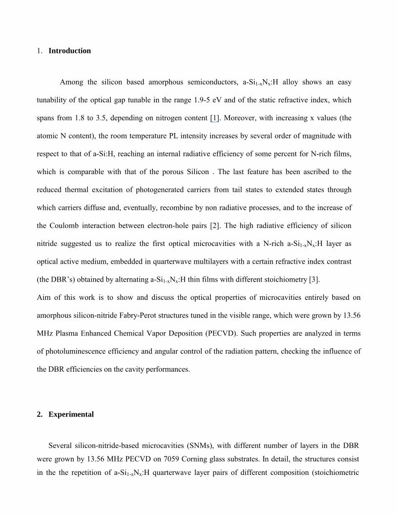
The abruptness of the interface between a-Si1-xNx:H layers with different N content is shown in
fig.1. The interface roughness of the deposited SNMs can be estimated in the range of few Ă,
warranting the structural quality of the multilayers.
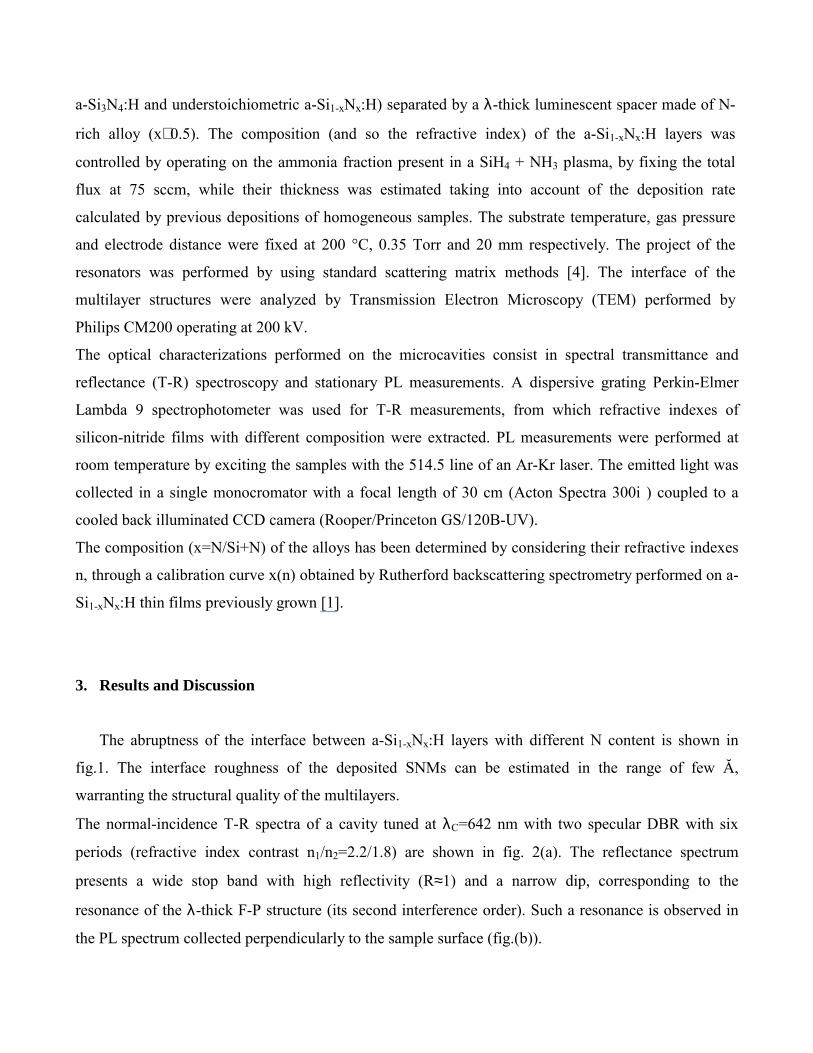
The normal-incidence T-R spectra of a cavity tuned at λC=642 nm with two specular DBR with six
periods (refractive index contrast n1/n2=2.2/1.8) are shown in fig. 2(a). The reflectance spectrum
presents a wide stop band with high reflectivity (R≈1) and a narrow dip, corresponding to the
resonance of the λ-thick F-P structure (its second interference order). Such a resonance is observed in
the PL spectrum collected perpendicularly to the sample surface (fig.(b)).
The intensity of the PL resonant peak shows a noticeable quenching for collecting angles far from the
normal emission, as shown in the polar plot. In the same figure, the emission of a λ-thick single layer
with the same composition as that of the spacer embedded in the microcavity (N/(Si+N)=0.5) is shown
for comparison. The cavity signal present for λ > 700 nm is essentially due to the luminescence yield of
the high refractive index layers (with composition x=0.41) belonging to the DBRs.
Three effects can be noticed in the PL spectra of the microcavity: (a) a strong narrowing of the spacer
emission band (with a width ∆λ = 5 nm), (b) a noticeable luminescence yield enhancement at the
resonance wavelength (more than two order of magnitude with respect to the PL intensity of the spacer
without the cavity), (c) a marked directionality of the emitted light around a cone of 20°-30° with
respect to the axis normal to the stack surface (see the inset of fig. 2 (b)). This marked directionality
could explain the luminescence enhancement even in absence of an altered spontaneous emission rate,
never verified for such a kind of resonators [5]. Actually, the high efficiency of the DBRs which embed
the spacer surely induce an anisotropic density of the optical modes, thus allowing a spatial
redistribution of the spontaneous emission.
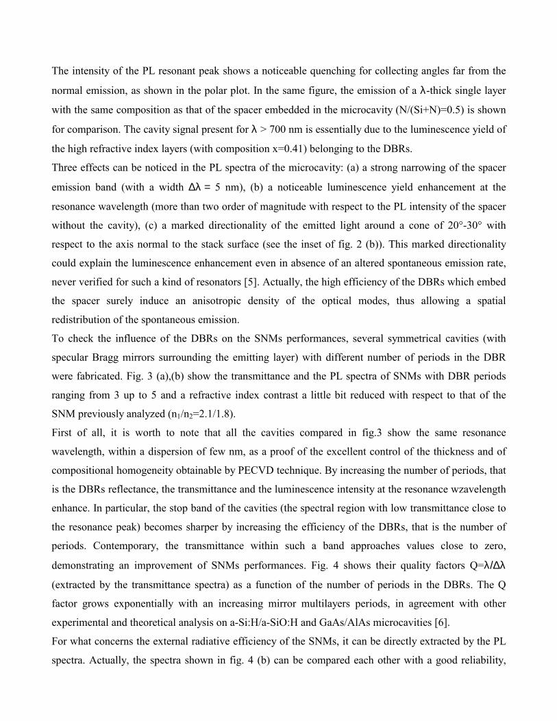
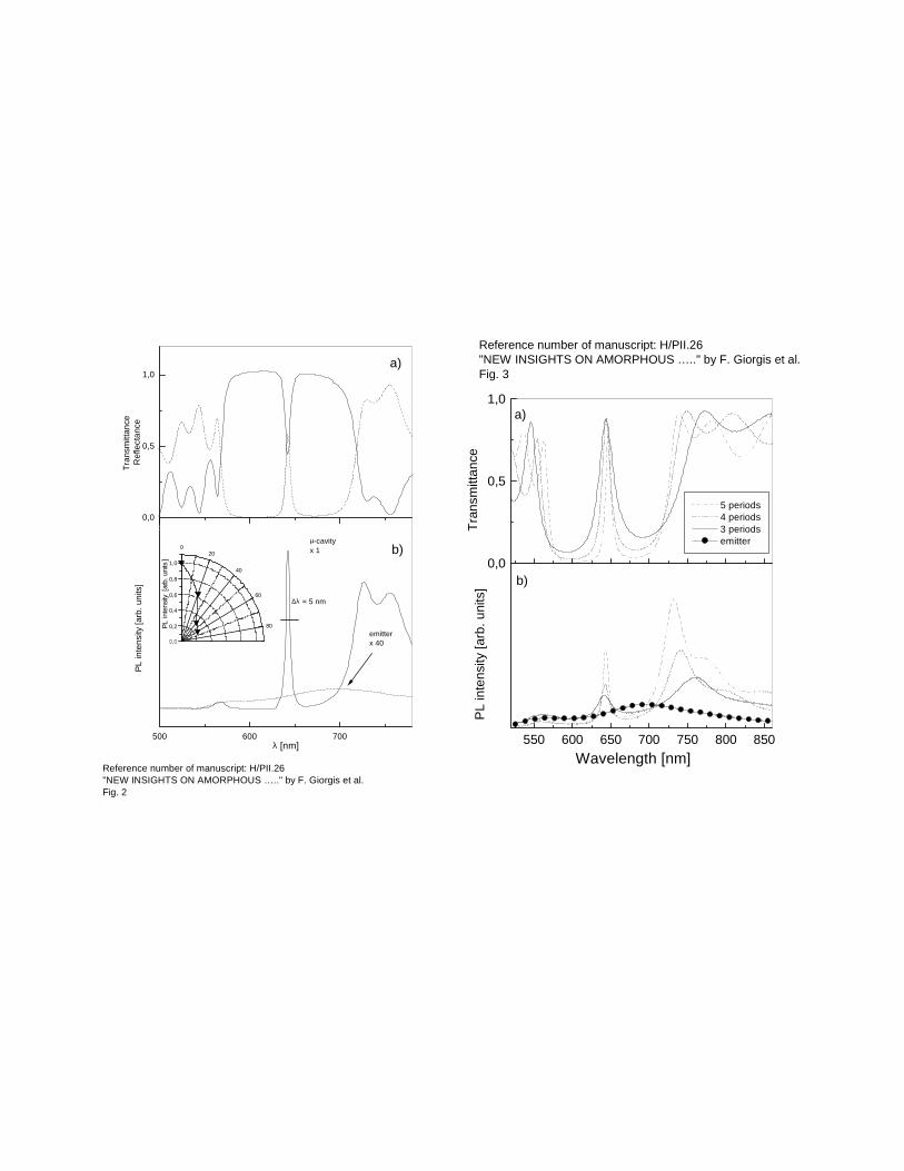
To check the influence of the DBRs on the SNMs performances, several symmetrical cavities (with
specular Bragg mirrors surrounding the emitting layer) with different number of periods in the DBR
were fabricated. Fig. 3 (a),(b) show the transmittance and the PL spectra of SNMs with DBR periods
ranging from 3 up to 5 and a refractive index contrast a little bit reduced with respect to that of the
SNM previously analyzed (n1/n2=2.1/1.8).
First of all, it is worth to note that all the cavities compared in fig.3 show the same resonance
wavelength, within a dispersion of few nm, as a proof of the excellent control of the thickness and of
compositional homogeneity obtainable by PECVD technique. By increasing the number of periods, that
is the DBRs reflectance, the transmittance and the luminescence intensity at the resonance wzavelength
enhance. In particular, the stop band of the cavities (the spectral region with low transmittance close to
the resonance peak) becomes sharper by increasing the efficiency of the DBRs, that is the number of
periods. Contemporary, the transmittance within such a band approaches values close to zero,
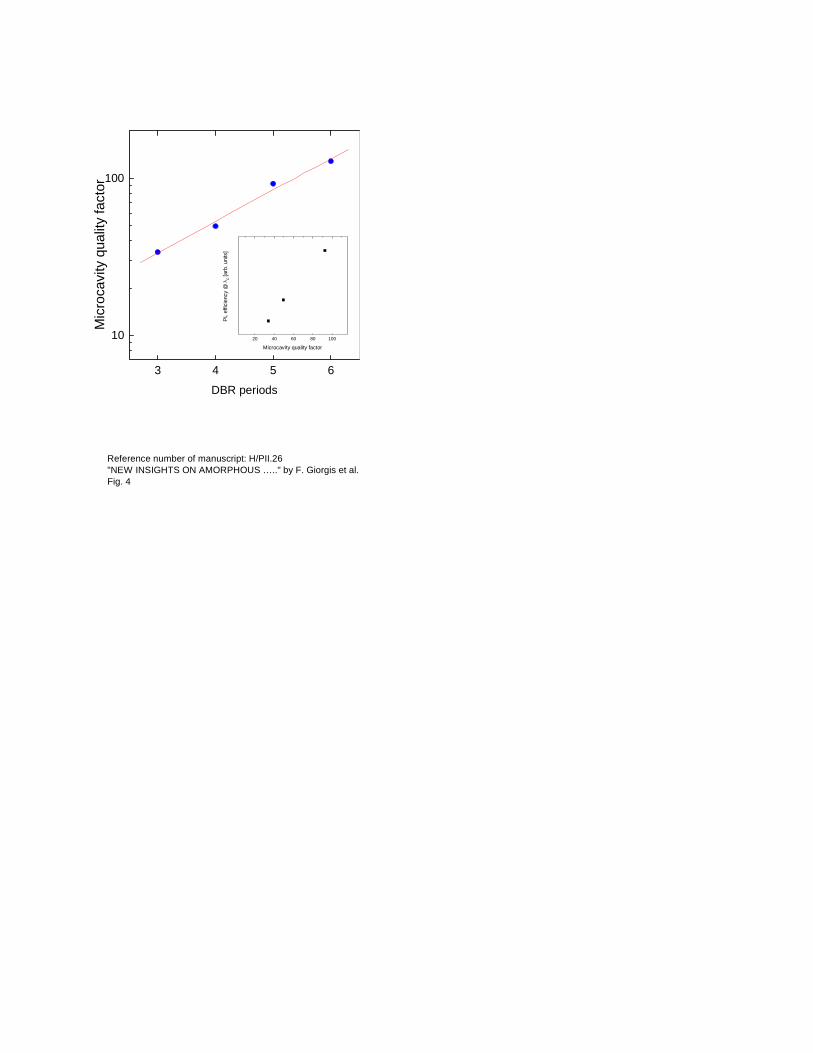
demonstrating an improvement of SNMs performances. Fig. 4 shows their quality factors Q=λ/∆λ
(extracted by the transmittance spectra) as a function of the number of periods in the DBRs. The Q
factor grows exponentially with an increasing mirror multilayers periods, in agreement with other
experimental and theoretical analysis on a-Si:H/a-SiO:H and GaAs/AlAs microcavities [6].
For what concerns the external radiative efficiency of the SNMs, it can be directly extracted by the PL
spectra. Actually, the spectra shown in fig. 4 (b) can be compared each other with a good reliability,
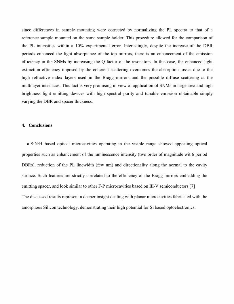
since differences in sample mounting were corrected by normalizing the PL spectra to that of a
reference sample mounted on the same sample holder. This procedure allowed for the comparison of
the PL intensities within a 10% experimental error. Interestingly, despite the increase of the DBR
periods enhanced the light absorptance of the top mirrors, there is an enhancement of the emission
efficiency in the SNMs by increasing the Q factor of the resonators. In this case, the enhanced light
extraction efficiency imposed by the coherent scattering overcomes the absorption losses due to the
high refractive index layers used in the Bragg mirrors and the possible diffuse scattering at the
multilayer interfaces. This fact is very promising in view of application of SNMs in large area and high
brightness light emitting devices with high spectral purity and tunable emission obtainable simply
varying the DBR and spacer thickness.
4. Conclusions
a-SiN:H based optical microcavities operating in the visible range showed appealing optical
properties such as enhancement of the luminescence intensity (two order of magnitude wit 6 period
DBRs), reduction of the PL linewidth (few nm) and directionality along the normal to the cavity
surface. Such features are strictly correlated to the efficiency of the Bragg mirrors embedding the
emitting spacer, and look similar to other F-P microcavities based on III-V semiconductors [7]
The discussed results represent a deeper insight dealing with planar microcavities fabricated with the
amorphous Silicon technology, demonstrating their high potential for Si based optoelectronics.
References
[1] F. Giorgis, C.F. Pirri, E. Tresso, Thin Solid Films 307 (1997) 298.
[2] F. Giorgis, C. Vinegoni, L. Pavesi, Phys. Rev. B 61 (2000) 4693.
[3] F. Giorgis, Appl. Phys. Lett. 77 (2000) 522.
[4] E. Hecht, Optics (Addison-Wesley Publishing, 1987) p. 373.
[5] F. Giorgis, S. Ferrero, P. Mandracci, C. F. Pirri, M. Cazzanelli and L. Pavesi, Mat. Research Soc.
Proc., Vol. 637 (2001) E 2.7.
[6] V. G. Golubev, A. A. Dukin, A. V. Medvev, A. B. Pevtsov, A. V. Sel’kin, N. A. Feoktistov,
Semiconductors 35 (2001) 1213.
[7] G. Björk, S. Machida, Y. Yamamoto, K. Igeta, Phys. Rev. A 44, 669 (1991).
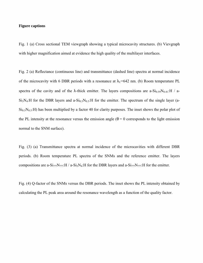
Figure captions
Fig. 1 (a) Cross sectional TEM viewgraph showing a typical microcavity structures. (b) Vievgraph
with higher magnification aimed at evidence the high quality of the multilayer interfaces.
Fig. 2 (a) Reflectance (continuous line) and transmittance (dashed line) spectra at normal incidence
of the microcavity with 6 DBR periods with a resonance at λC=642 nm. (b) Room temperature PL
spectra of the cavity and of the λ-thick emitter. The layers compositions are a-Si0.59N0.41:H / a-
Si3N4:H for the DBR layers and a-Si0.5N0.5:H for the emitter. The spectrum of the single layer (a-
Si0.5N0.5:H) has been multiplied by a factor 40 for clarity purposes. The inset shows the polar plot of
the PL intensity at the resonance versus the emission angle (θ = 0 corresponds to the light emission
normal to the SNM surface).
Fig. (3) (a) Transmittance spectra at normal incidence of the microcavities with different DBR
periods. (b) Room temperature PL spectra of the SNMs and the reference emitter. The layers
compositions are a-Si???N???:H / a-Si3N4:H for the DBR layers and a-Si???N???:H for the emitter.
Fig. (4) Q-factor of the SNMs versus the DBR periods. The inset shows the PL intensity obtained by
calculating the PL peak area around the resonance wavelength as a function of the quality factor.
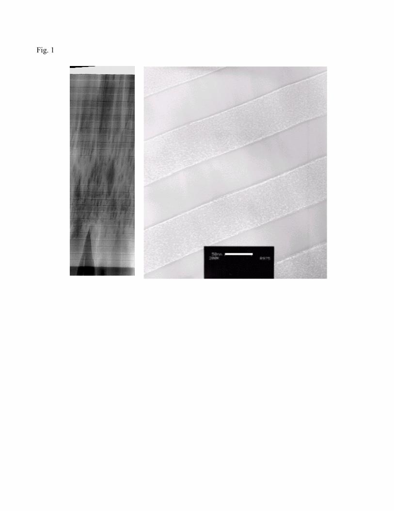
Fig. 1
50 nm
a) b)
500 600 700
b)
Reference number of manuscript: H/PII.26"NEW INSIGHTS ON AMORPHOUS ….." by F. Giorgis et al.Fig. 2
∆λ = 5 nm
µ-cavityx 1
emitterx 40
λ [nm]
PL in
tens
ity [a
rb. u
nits
]
500 600 700
0,0
0,5
1,0a)
020
40
60
80
0,0
0,2
0,4
0,6
0,8
1,0
0,0
PL in
tens
ity [a
rb. u
nits]
Tran
smitt
ance
Ref
lect
ance
550 600 650 700 750 800 850
0,0
0,5
1,0
Reference number of manuscript: H/PII.26"NEW INSIGHTS ON AMORPHOUS ….." by F. Giorgis et al.Fig. 3
b)
Wavelength [nm]
5 periods 4 periods 3 periods emitter
PL in
tens
ity [a
rb. u
nits
]
a)
Tran
smitt
ance
20 40 60 80 100
3 4 5 6
10
100
Reference number of manuscript: H/PII.26"NEW INSIGHTS ON AMORPHOUS ….." by F. Giorgis et al.Fig. 4
PL e
ffici
ency
@ λ
C [ar
b. u
nits
]
Microcavity quality factor
M
icro
cavi
ty q
ualit
y fa
ctor
DBR periods