NEAR EAST UNIVERSITY Faculty of Engineering
95
NEAR EAST UNIVERSITY Faculty of Engineering Department of Electrical and Electronic Engineering ALARM SYSTEMS BY USING WITH ELECTRONIC COMPONENTS Graduation Project EE-400 Student: Mehmet Ali Dolap (990293) Supervisor: Ozgiir Cemal Ozerdem Lefkosa - 2004
-
Upload
khangminh22 -
Category
Documents
-
view
1 -
download
0
Transcript of NEAR EAST UNIVERSITY Faculty of Engineering

NEAR EAST UNIVERSITY
Faculty of Engineering
Department of Electrical and Electronic Engineering
ALARM SYSTEMS BY USING WITH ELECTRONIC COMPONENTS
Graduation Project EE-400
Student: Mehmet Ali Dolap (990293)
Supervisor: Ozgiir Cemal Ozerdem
Lefkosa - 2004

TABLE OF CONTENTS
_.\CKNOWLEDGEMENT .i _.\BSTRACT .ii ;IRODUCTION .iii
CHAPTER:1 1 I .TRANSISTORS .1 1.1 Introduction to transistors? I 1.2 History of Transistors 1 1. 3 How do transistors work? 1 1.4 How do holes and electrons conduct in transistors? 2 1.5 Transistor amplification .4 1.6 NPN Transistor Operation .4 1.7 FET's as transistors .10 1. 8 How are semiconductors made? .10 1.9 Construction 11
CHAPTER :2 13 2.RESISTORS 13 2.1 Introduction 13 2.2 Type ofResistors 13 2. 3 .Low power resistors 16 -2.4 High power resistors 17 2.5 Variable resistors 17 2.6 Resistor Color Coding .18
CHAPTER:3 23 3.CAPACITOR 23 3 .1 How Charge is Stored in The Dielectric 23 3 .2 Changing and Discharging a Capacitor 24 3.3 The Farad Unit of Capacitance 27 3.4 Typical Capacitors , 30 3.5 Electrolytic Capacitors 35 3.6 Capacitor Color Coding 37 3.7 Parallel Capacitances 39 3. 8 Series Capacitances .40 3.9 Stray Capacitive and Inductive Effects .41 3.10 How to read a capacitor .45 3 .11 Capacitor codes 46
CHAPTER:4 48 4 DIODES 48 4.1 Semiconductor Diodes .48 -4.2 Special Purpose Diodes 50

CHAPTER:5 55 5 CD4001 BC OF GATE 55 5.1 General Description 55 5.2 Features 55 5.3 Ordering Code 55 5 .4Connection Diagrams 5 6 5.6 Schematic Diagrams 56 5.7 Absolute Maximum Ratings 57 5.8Recommended Operating Conditions 57 5.9 DC Electrical Characteristics 57 5.10 AC Electrical Characteristics 58 5.11 AC Electrical Characteristics : 58 5.12 Typical Transfer Characteristics 59 5.13 Typical Performance Characteristics 60 5.14 Typical Performance Characteristics 61 5.15 Physical Dimensions 62
CHAPTER:6 65 6.1 Flip flop 65 6.2 Master-Slave D Flip-flops 68 6.3 Master-Slave JK Flip-flops Circuit Structure and Operation 70 6.4 Edge-triggered D Flip-flops 72 6.5 Edge-triggered JK Flip-flops 77 6.6 T Flip-flops Edge-triggered T Flip-flop 79 6.7 Latch and Flip-flop Summary 81
CHAPTER: 7 82 7 THE CIRCUIT OF ALARM SYSTEMS AND PICTURES 82 7.1 Low Power Alarm , 82 7.2 High Power Alarm 84 7.3 Pulsed Tone Alarm 84 7.4 One Shot Alarm 85 7.5 Picture 86
CONCLUSION 88 REFERENCES 89

ACKNOWLEDGEMENTS
.Ii is my pleasure to take this opportunity to express my greatest gratitude to many
individuals who have given me a lot if supports during my faur-year Undergraduate program in
the Hear .East University. #'/thou! them, my Graduation Prqject would not have been succes{/it!(y
completed on time.
First o/'. all, / would like to e.,ipress my thanlcs to my supervisor Afr. Ozgtlr Cema! Ozerdem
far supervising my prqject. Under the guidance o/'. him/ succes{/it!(y overcome many d(/jicu!ties
and/ learned a lot about e!ectromc. /n each discussion, he used to e.,ip!ain the problems and
answer my questions. He always helped me a lot and/ flit remarkable progress during his supervision.
/ thank Assist. Pref. .Dr. Kadri .8tlnlnctilc far giving his time to me far doing my
registirations, and/ thank Pref.Dr. ,Yeno! .8ekla:f far helping with our problems in school, / thank
Pref. .Dr Fakhreddin Mamedov far helping us with our problems in our department.
,,., ,i( •·'
/ also want to thank all my .friends and .specia!(y ..Ercan .Dursun,A!i Kurtekhn,MHedim
Perihanog!u,.8ahadtr Kara who supported and helped me all the time.
Finally, .special thanlcs far my family, e.special(y my parents far being patient/it! during my
1U1dergraduate degree stuay. / could never have completed my study without their encouragement
mrd endless support.

ABSTRACT
Electronic components are internal organs of electronic and electrical circuit. For the
engineering knowledge of electronic components is very important to design many applications with electronic devices.
Electronic devices makes easier for the activication of people. We can say some
applications for example , robotic devices , communication systems , illumating systems ... etc.
Also there are many kind of these application . In the real life everytime we need to these electronic devices.
While working in the topic of electrical and electronic components. Everyone, technicians
or engineers should be very careful because small mistakes can cause big damages in application.
Therefore these reasons electronic and electrical very important for our life. We can not think a life less electronic and electric.
11
..• •r.

INTRODUCTION
For most part,the subject of electronic devices means semiconductor devices such as
transistor, diodes and integrated circuits. They are used for amplifiers,oscillators,rectifiers and
digital circuits which include just about everything in electronics. The semiconductors are a
group of chemical elements with special electrical characteristic most common are are silicon
(si) and germanium (Ge) with Si used for almost all semiconductors components.The
semiconductors have unique atomic structure that allows the addition of specific impurity
elements to produce very useful features that can be applied in electronic circuits.
Resistors are probably the most common components in electronic equipment.A resistor is
manufactured with specific value of ohms for its resistance (R). The purpose of using a
resistor in circuit is either to reduce current I to a specific value or to provide a desied
voltageV.The feature ofresistance that the effect is the same for de and ac circuits. 't'!
Capacitance is the ability of a dielectric to store electric charge. The more the charge that is
stored for a given voltage , the higher the value o capacitance.Its symbol is C and units is the
Farad (F) .Acapacitor consists of an insulator betwen two conductors. Common types are
air,ceramic,mica,paper,plastic and electrolytic capacitors. Capacitors used in electronic circuits are small and economical.
lll
CHAPTER: 1
1.TRANSISTORS
1.1 Introduction to transistors?
Transistors, I was once told, "were the fastest acting fuse known to mankind". This of
course was a reference to the fact an early transistor was intolerant of fault conditions whereas
in years gone by, vacuum tubes (valves) would cop a lot of abuse. Just remember that fact.
[one of "murphy's laws" - The component exists to protect the fuse]
Generally transistors fall into the category of bipolar transistor, either the more common
~N bipolar transistors or the less common PNP transistor types. There is a further type
known as a FET transistor which is an inherently high input impedance transistor with
behaviour somewhat comparable to valves. Modern field effect transistors or FET's including
JFETS and MOSFETS now have some very rugged transistor devices. I am often asked about the term "bipolar" - see later.
1.2 History of Transistors
The transistor was developed at Bell Laboratories in 1948. Large scale commercial use
didn't come until much later owing to slow development. Transistors used in most early
entertainment equipment were the germanium types. When the silicon transistor was
veloped it took off dramatically. The first advantages of the transistor were relatively low
power consumption at low voltage levels which made large scale production of portable
entertainment devices feasible. Interestingly the growth of the battery industry has paralleled
growth of the transistor industry. In this context I include integrated circuits which of
urse are simply a collection of transistors grown on the one silicon substrate.
1.3 How do transistors work?
Transistors work on the principle that certain materials e.g. silicon, can after processing be
e to perform as "solid state" devices. Any material is only conductive in proportion to the
ber of "free" electrons that are available. Silicon crystals for example have very few free
1

electrons. However if "impurities" (different atomic structure - e.g. arsenic) are introduced in
a controlled manner then the free electrons or conductivity is increased. By adding other
impurities such as gallium, an electron deficiency or hole is created. As with free electrons,
the holes also encourage conductivity and the material is called a, semi-conductor.
Semiconductor material which conducts by free electrons is called n-type material while
material which conducts by virtue of electron deficiency is called_p-ty_pematerial.
1.4 How do holes and electrons conduct in transistors?
If we take a piece of the p-type material and connect it to a piece of n-type material and apply
voltage as in figure 1.4.1 then current will flow. Electrons will be attracted across the junction
of the p and n materials. Current flows by means of electrons going one way and holes going
in the other direction. If the battery polarity were reversed then current flow would cease.
,: current
~ ++++++ ++++++ 1. p , ....... p +++++++ ++++++ ++++++ +++++++ +++++++ ++++++ ++++++ ------ , - N ------
N i------- ------- ------ ------ ------- -------· ,,
Figure 1.4.1 - electron flow in a p-n juction of a diode
Some very interesting points emerge here. As depicted in figure 1.4.1 above a junction of p
d n types constitutes a rectifier diode. Indeed a transistor can be configured as a diode and
ften are in certain projects, especially to adjust for thermal variations. Another behaviour
· ch is often a limitation and at other times an asset is the fact that with zero spacmg
een the p and n junctions we have a relatively high value capacitor.
This type of construction places an upper frequency limit at which the device will operate.
· was a severe early limitation on transistors at radio frequencies. Modem techniques have
course overcome these limitations with some bipolar transistors having Ft's beyond 1 Ghz.
capacitance at the junction of a diode is often taken advantage of in the form of varactor
s. See the tutorial on diodes for further details. The capacitance may be reduced by
· g the junction area of connection as small as possible. This is called a "point contact".
2

Now a transistor is merely a "sandwich" of these devices. A PNP transistor is depicted in
figure 1.4.2 below.
Cbe Cbc
Figure 1.4.2. - sandwich construction of a PNP transistor
Actually it would be two p-layers with a "thin" n-layer in between. What we have here are
two p-n diodes back to back. If a positive voltage (as depicted) is applied to the emitter,
current will flow through the p-n junction with "holes" moving to the right and "electrons
moving to the left. Some "holes" moving into the n-layer will be neutralised by combining
with the electrons. See electron theory and atoms. Some "holes" will also travel toward the
right hand region.
The fact that there are two junctions leads to the term "bipolar transistor".
If a negative voltage (as depicted) is applied to the collector of the transistor, then ordinarily
no current flows BUT there are now additional holes at the junction to travel toward point 2
and elctrons can travel to point 1, so that a current can flow, even though this section is biased
to prevent conduction.
It can be shown that most of the current flows between points 1 and 2. In fact the amplitude
(magnitude) of the collector current in a transistor is determined mainly by the emitter current
which in tum is determined by current flowing into the base of the transistor. Consider the
base to ~e a bit like a tap or faucet handle.
.)

1.5 Transistor amplification
Because the collector current (where the voltage is relatively high) is pretty much the same
as the emitter current and also controlled by the emitter current (where the voltage is usually
much lower) it can be shown by ohms law
P=I2XR that amplification occurs. See small signal amplifiers
1.6 NPN Transistor Operation
Just as in the case of the PN junction diode, the N material comprising the two end sections
of the NP N transistor contains a number of free electrons, while the center P section contains
an excess number of holes. The action at each junction between these sections is the same as
that previously described for the diode; that is, depletion regions develop and the junction
barrier appears. To use the transistor as an amplifier, each of these junctions must be modified
by some .external bias voltage. For the transistor to function in this capacity, the first PN
junction (emitter-base junction) is biased in the forward, or low-resistance, direction. At the
same time the second PN junction (base-collector junction) is biased in the reverse, or high
resistance, direction. A simple way to remember how to properly bias a transistor is to
observe the NPN or PNP elements that make up the transistor. The letters of these elements
indicate what polarity voltage to use for correct bias. For instance, notice the NPN transistor
show belowfigure: 1.6.1:
Figure: 1.6.l
4

The emitter, which is the first letter in the NPN sequence, is connected to the negative side
of the battery while the base, which is the second letter(NE.N), is connected to the positive
side. However, since the second PN junction is required to be reverse biased for proper
transistor operation, the collector must be connected to an opposite polarity voltage/positive)
than that indicated by its letter designation(NPN). The voltage on the collector must also be
more positive than the base, as shown below figure: 1.6.2:
Figure: 1.6.2
We now have a properly biased NPN transistor.
In summary, the base of the NE.N transistor must be positive with respect to the emitter, and
the collector must be more positive than the base.
NPN FORWARD-BIASED JUNCTION. - An important point to bring out at this time,
which was not necessarily mentioned during the explanation of the diode, is the fact that the N
material on one side of the forward-biased junction is more heavily doped than the P material.
This results in more current being carried across the junction by the majority carrier electrons
from the N material than the majority carrier holes from the P material. Therefore, conduction
through. the forward-biased junction, as shown in figure 1.6.3, is mainly by majority carrier
electrons from the N material (emitter) .
5

Figure 1.6.3. - The forward-biased junction in an NPN transistor
With the emitter-to-base junction in the figure biased in the forward direction, electrons
leave the negative terminal of the battery and enter the N material (emitter). Since electrons
are majority current carriers in the N material, they pass easily through the emitter, cross over
the junction, and combine with holes in the P material (base). For each electron that fills a
hole in the P material, another electron will leave the P material ( creating a new hole) and
enter the positive terminal of the battery.
NPN REVERSE-BIASED JUNCTION. - The second PN junction (base-to-collector), or
reverse-biased junction as it is called (fig. 1.6.4), blocks the majority current carriers from
crossing the junction. However, there is a very small current, mentioned earlier, that does pass
through this junction. This current is called minority current, or reverse current. As you recall,
this current was produced by the electron-hole pairs. The minority carriers for the reverse
biased PN junction are the electrons in the P material and the holes in the N material. These
minority carriers actually conduct the current for the reverse-biased junction when electrons
from the P material enter the N material, and the holes from the N material enter the P
material. However, the minority current electrons (as you will see later) play the most
important part in the operation of the NPN transistor.
6

Figure 1.6.4. - The reverse-biased junction in an NPN transistor.
At this point you may wonder why the second PN junction (base-to-collector) is not forward
biased like the first PN junction (emitter-to-base). If both junctions were forward biased, the
electrons would have a tendency to flow from each end section of the N P N transistor
(emitter and collector) to the center P section (base). In essence, we would have two junction
diodes possessing a common base, thus eliminating any amplification and defeating the
purpose of the transistor. A word of caution is in order at this time. If you should mistakenly
ias the second PN junction in the forward direction, the excessive current could develop
enough heat to destroy the junctions, making the transistor useless. Therefore, be sure your
ias voltage polarities are correct before making any electrical connections.
NPN JUNCTION INTERACTION. - We are now ready to see what happens when we
e the two junctions of the NPN transistor in operation at the same time. For a better
derstanding of just how the two junctions work together, refer to figure 1.6.5 during the
USSlOn.
7

Figure 1.6.5. - NPN transistor operation.
The bias batteries in this figure have been labeled V cc for the collector voltage supply, and
V BB for the base voltage supply. Also notice the base supply battery is quite small, as
indicated by the number of cells in the battery, usually 1 volt or less. However, the collector
supply is generally much higher than the base supply, normally around 6 volts. As you will
see later, this difference in supply voltages is necessary to have current flow from the emitter
to the collector.
As stated earlier, the current flow in the external circuit is always due to the movement of
free electrons. Therefore, electrons flow from the negative terminals of the supply batteries to
the N-type emitter. This combined movement of electrons is known as emitter current (IE),
Since electrons are the majority carriers in the N material, they will move through the N
material emitter to the emitter-base junction. With this junction forward biased, electrons
:ontinue on into the base region. Once the electrons are in the base, which is a P-type
material, they become minority carriers. Some of the electrons that move into the base
recombine with available holes. For each electron that recombines, another electron moves
out through the base lead as base current IB ( creating a new hole for eventual combination)
and returns to the base supply battery V
8

The electrons that recombine are lost as far as the collector is concerned. Therefore, to make
the transistor more efficient, the base region is made very thin and lightly doped. This reduces
the opportunity for an electron to recombine with a hole and be lost. Thus, most of the
electrons that move into the base region come under the influence of the large collector
reverse bias. This bias acts as forward bias for the minority carriers (electrons) in the base
and, as such, accelerates them through the base-collector junction and on into the collector
region. Since the collector is made of an N-type material, the electrons that reach the collector
again become majority current carriers. Once in the collector, the electrons move easily
through the N material and return to the positive terminal of the collector supply battery V cc
as collector current (le).
To further improve on the efficiency of the transistor, the collector is made physically larger
than the base for two reasons: (1) to increase the chance of collecting carriers that diffuse to
side as well as directly across the base region, and (2) to enable the collector to handle
re heat without damage.
In summary, total current flow in the NPN transistor is through the emitter lead. Therefore,
terms of percentage, IE is 100 percent. On the other hand, since the base is very thin and
tly doped, a smaller percentage of the total current ( emitter current) will flow in the base
uit than in the collector circuit. Usually no more than 2 to 5 percent of the total current is
current (IB) while the remaining 95 to 98 percent is collector current (le). A very basic
ionship exists between these two currents:
simple terms this means that the emitter current is separated into base and collector
t, Since the amount of current leaving the emitter is solely a function of the emitter-base
and because the collector receives most of this current, a small change in emitter-base
will have a far greater effect on the magnitude of collector current than it will have on
current. In conclusion, the relatively small emitter-base bias controls the relatively large
-to-collector current.
9

1.7 FET's as transistors
In figure 1.7 below I have depicted the schematics of the two most popular types. A J-FET
and a dual gate mosfet. Typical types might be MPF-102 for a J-FET and the old RCA 40673
for the dual gate.
G~
J-FET
G~D G1
s DG MOSFET
Figure 1. 7. - schematic of J-FET transistor and dual gate mosfet transistor
The PET of course is characterised by its extremely high input impedance. Some people
claim the PET is a superior device to a bipolar transistor. I consider that to be a subjective
opinion with the proviso that PET development has led to some amazing developments,
particularly with power-fets.
I won't go into any length about how PETS operate except to point out the principal
differences to NPN and PNP transistors. A bipolar transistor has moderate input impedance
( depending on configuration) while some FETs can and do have input impedances measured
in megohms. Bipolar transistors are essentially "current" amplifiers while PETS could be
:onsidered voltage amplifiers.
1.8 How are semiconductors made?
Strictly speaking this tutorial presented by Harris Semiconductor applies more to integrated
· ·cuits but the principle remains much the same.
The process of manufacturing semiconductors, or integrated circuits ( commonly called I Cs, or
· ps) typically consists of more than a hundred steps, during which hundreds of copies of an
egrated circuit are formed on a single wafer.
Generally, the process involves the creation of eight to 20 patterned layers on and into the
rate, ultimately forming the complete integrated circuit. This layering process creates
· cally active regions in and on the semiconductor wafer surface.
10

1.9 CONSTRUCTION
The very first transistors were known as point-contact transistors. Their construction is
similar to the construction of the point-contact diode covered in chapter 1. The difference, of
urse, is that the point-contact transistor has two P or N regions formed instead of one. Each
,f the two regions constitutes an electrode ( element) of the transistor. One is named the
emitter and the other is named the collector, as shown in figure 1.9, view A.
:,,
Figure 1.9. - Transistor constructions
int-contact transistors are now practically obsolete. They have been replaced by junction
1 sisters, which are superior to point-contact transistors in nearly all respects. The junction
I
~or generates less noise, handles more power, provides higher current and voltage gains,
can be mass-produced more cheaply than the point-contact transistor. Junction transistors
manufactured in much the same manner as the PN junction diode discussed earlier.
ver, when the PNP or NPN material is grown (view B), the impurity mixing process
be reversed twice to obtain the two junctions required in a transistor. Likewise, when the
,-junction (view C) or the diffused-junction (view D) process is used, two junctions must
created within the crvstal.
11

Although there are numerous ways to manufacture transistors, one of the most important
parts of any manufacturing process is quality control. Without good quality control, many
transistors would prove unreliable because the construction and processing of a transistor
govern its thermal ratings, stability, and electrical characteristics. Even though there are many
variations in the transistor manufacturing processes, certain structural techniques, which yield
good reliability and long life , are common to all processes: (1) Wire leads are connected to
each semiconductor electrode; (2) the crystal is specially mounted to protect it against
mechanical damage; and (3) the unit is sealed to prevent harmful contamination of the crystal.
12

CHAPTER :2
2.RESISTORS
2.1 Introduction
The resistor is one of the most diverse and easiest of all the electrical components you will
find in your average radio or TV set. This is because it has been around for many years and
plays such a vital role that it will continue to in many new shapes and sizes to come. Today
there are many different resistors in circulation, all of which will be explained shortly but for
now lets go over some of the most important details.
The resistor is a component that has one purpose and that is to resist current and voltage by
means of combining conductive material with a nonconductive one to form a substance that
allows electrons to flow through its self but not as efficiently as a typical wire. The unit of
measuring how much the resistor will oppose current is measured in ohms and to determine
the outcome of the resistor we would use mathematical formulas known as ohms law.
There are three main types of resistors, which can then be broken down into other categories
but lets first look at the three main types.
2.2 TYPES OF RESISTORS
The two main characteristics of a resistor are its resistance .R in ohms and its power rating lf'in -,
watts. Resistors are available in a very wide range of ./?values, from a fraction of an ohm to many
kilohms (kO) and megohms (MO). One kilohm is 1000 0, and one megohm is 1,000,000 n. More details of very small and large units are given in Chap. 3. The power rating for resistors
may be as high as several hundred watts or as low as ///OW.
The .R is the resistance value required to provide the desired current 7 or voltage. Also
· portant is the wattage rating, because it specifies the maximum power the resistor can
· sipate without excessive heat. Dissipation means that the power is wasted, since the resultant
beat is not used. Too much heat can make the resistor burn. The wattage rating of the resistor is
erally more than the actual power dissipation, as a safety factor.
13

Most common in electronic equipment are carbon resistors with a power rating of 1 W or less.
The construction is illustrated in Fig. 2.2.1, while Fig. 2.2.2 shows a group of resistors to be
mounted on a printed-circuit (PC) board. Toe resistors can be inserted automatically by
machine.
lal
fb)
Figure:2.2.1
Fig. 2.2.1 Carbon-composition resistors, (a) Internal construction. Length is 3/4 in. without
leads for 1-W power rating. Color stripes give ..R in ohms. Tinned leads have coating of solder,
(b) Group of resistors and transistors mounted on printed-circuit (PC) board. The printed-circuit
conductors are on the opposite side. (Direct Positive ./magel);) i.'
Figure:2.2.2
Fig. 2.2.2 Typical carbon resistors commonly used on PC board. Leads are cut and formed
insertion into holes with 0.5 in. spacing.
Resistors with higher ..R values usually have lower wattage ratings because they have less
nt. As an example, a common value is 1 Mn at 1/4 W, for a resistor only //2in. long. The
14
lower the power rating, the smaller the actual physical size of the resistor. However, the
resistance value is not related to physical size.
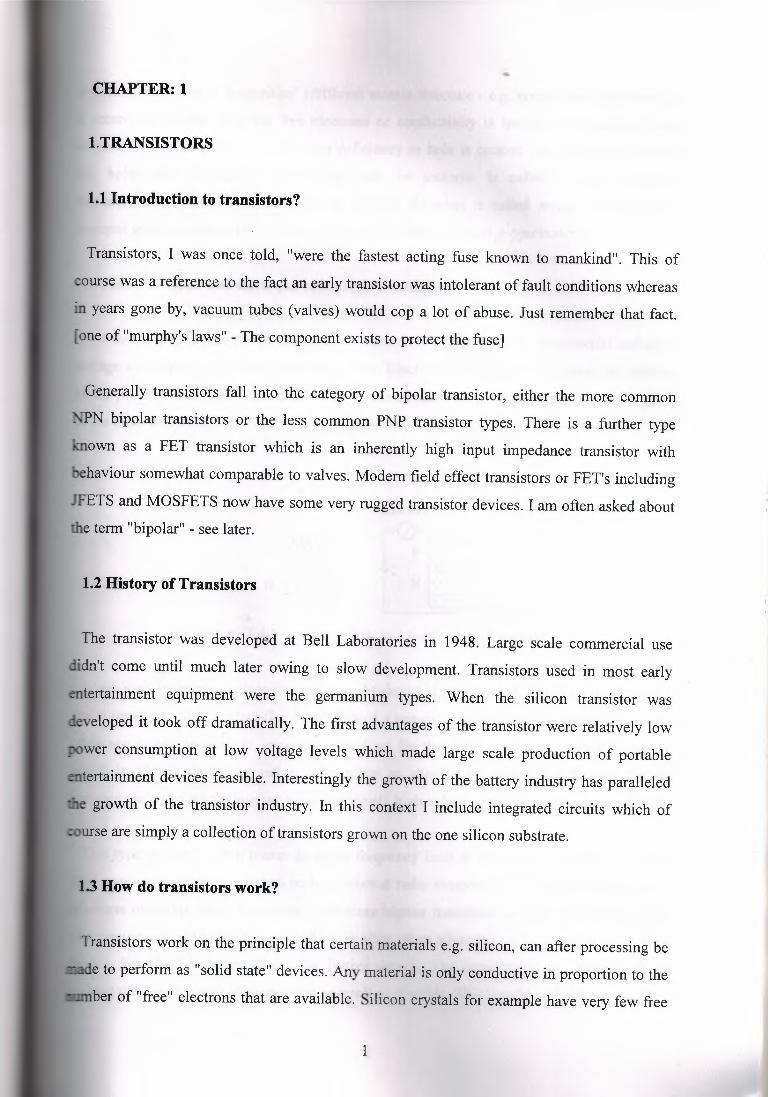
Wire-Wound Resistors In this construction, a special type of wire called resistance wire is
wrapped around an insulating core, as shown in Fig. 2.2.3. Tue length of wire and its specific
resistivity determine the l?ofthe unit.
( a) (b)
Fig. 2.2.3 Large wire-wound resistors with 50-W power rating.
Since they are generally for high-current applications with low resistance and appreciable
power, wire-wound resistors are available in wattage ratings from 5 W up to 100 W or more.
The resistance can be less than 1 0 up to several thousand ohms. I ., ...
In addition, wire-wound resistors are used where accurate, stable resistance values are
necessary. Examples are precision resistors for the function of an ammeter shunt or a precision
potentiometer to adjust for an exact amount of .R.
For 2 W or less, carbon resistors are preferable because they are small and cost less. Between
2 and 5 rW, combinations of carbon resistors can be used. Also, small wire-wound resistors are
available in a 3- or 4-W rating.
Carbon-Composition Resistors This type of resistor is made of finely divided carbon or
graphite mixed with a powdered insulating material as a binder, in the proportions needed for
the desired l?value. As shown in Fig. 2.2.3 large, the resistor element is enclosed in a plastic case
for insulation and mechanical strength. Joined to the two ends of the carbon resistance element are
metal caps' with leads of tinned copper wire for soldering the connections into a circuit. These
are called axial leads because they come straight out from the ends. Carbon resistors are
commonly available in l?values of 10 to 20 MO. Examples are 10 ft, 220 ft, 4.7 k.Q, and 68
kn. The power rating is generally ///0, //8, //4, 1, or 2 W.
15

Film-Type Resistors There are two kinds of film-type resistors. The carbon-film type has a
thin coating around an insulator. Metal-film resistors have a'spiral around a ceramic substrate (Fig.
2.2.4). Their advantage is more precise I? values. The film-type resistors use metal end caps for
the terminal leads, which ihakes the ends a little larger than the body.
Epoxy Metal film coating
Fig. 2.2.4 Construction of metal-film resistor. (.Stackpole Copora!ioJV
Chip Resistors These have a carbon coating fired onto a solid ceramic substrate. The purpose
is to have more precise I? values and greater stability with temperature changes. They are often
made in a small square with leads to fit a printed circuit (PC) board.
Fusible Resistors This type is a wire-wound resistor made to burn open easily when the
power rating is exceeded. It then serves the dual functions of a fuse and a resistor to limit the
current.
2.3 Low power resistors
The carbon film resistor is composed up of a resistive material like graphite that is then cut
into blocks or wrapped, or grafted in a desired way. For example, the length of the resistive
material will determine how much resistance there will be while the width of the resistive
material will determine what kind of power it can handle, the wider the more power it can
handle. The schematic symbol can be seen in the picture to the right while the different types
of carbon film resistors can be seen below. There are some three distinct types of carbon film
resistors which as follows:
-The standard film resistor (A)- a circular resistor with two pins extending from opposite sides
the barrel- shaped resistor. -The chip resistor (B)- this type of resistor was introduced in the late 80's to accommodate for
ever shrinking computer components where there can be up to 6 layers per circuit board.
16

• network resistor (C)- this type of resistor comes in (SIPP) form and can contain up to 12
· ors in a compact space that can not compare
Figure: 2.3
High power resistors
The most common wire wound resistor is composed up a fairly resistive wire wrapped
und a ceramic cylinder and typically has a power range form 5 to 50 watts and is most
found in power supplies and amplifiers. It is common to find these components to heat
to levels that bums to the touch and is why they are made up of ceramic, a fire resistant
terial. The schematic symbol is the same of the carbon film resistor so it is also quite easy
remember.
, .. -~
The box to the right shows some typical wire wound resistors and more information can be
don each one by clicking on its figure: 2.4.
Figure: 2.4
2.5 Variable resistors
The variable resistor is a very important component that is found in many electrical for such
· gs as tone and bass controls as well as volume. This is due to the fact that resistors can be
17

joined together with other components to form filters for a desired levels. They can also be
found in computer monitors for color or positioning as well as the dimming switch for your
lamps.
This is done through digital to analog and analog to digital circuits, one great advantage to
this is that you are able to tum a knob instead of typing a value in every time you want to
change the tint or brightness.
The schematic for the variable resistor has stayed the same for quite some time and can be
seen at the illustration to the upper right. As you see it looks somewhat like a typical resistor
but is an arrow coming out from one side pointing to the center of the resistor. For more
details on such questions like How does it work?, How do I use it?, and other such questions
click on any illustration of your choice below.
Figure: 2.5
2.6 RESISTOR COLOR CODING
Because carbon resistors are small physically, they are color-coded to mark their /? value in
ohms. The basis of this system is the use of colors for numerical
Figure:2.6
18

Table 2.6 Color Code
1st Figure
Band2 2nd Figure
Band3 3rd Figure
Band4 Band 1
Tolerance
105
- - 106
J L l1 ~7 I I .ii
I 8 IE J ~ -----i1 i---
10-I
- - 10-2
L :r- 20%
values, as listed in Table 2.6. In memorizing the colors, note that the darkest colors, black and
brown, are for the lowest numbers, zero and one, whereas white is for nine. The color coding is
19

' standardized by the Electronic Industries Association (EIA). These colors are also used for small
capacitors, as summarized in App. B on all the color codes.
Resistance Color Stripes The use of bands or stripes is the most common system for color
coding carbon resistors, as shown in Fig. 2.6.1. Color stripes are printed at one end of the
insulating body, which is usually tan. Reading from left to right, the first band close to the edge
gives the first digit in the numerical value of .R. The next band marks the second digit. The third
band is the decimal multiplier, which gives the number of zeroes after the two digits.
In Fig. 2.6.2 a, the first stripe is red for 2 and the next stripe is green for 5. The red multiplier in
the third stripe means add two zeroes to 25, or "this multiplier is 102." The result can be
illustrated as.follows:
Band A first digit
Band 8 second digit
Band C decimal multiplier
Band D { Gold 5% tolerance Silver 10%
Fig. 2.6.1 How to read color stripes on carbon resistors for .Rin ohms.
Red i 2
Green t 5 X
Red .J. 100 2500
Therefore, this R value is 2500 n. R,.250±5% Red Green Black Gold
R •• 2.5 0 ± 10% Red
R •• 2500 O ± 50/o Red Green
Red Gold
~) ~) ~
Fig. 2.6.2 Examples of color-coded .Rvalues, with percent tolerance.
The example in Fig. 2. 6.2b illustrates that black for the third stripe just means "do not add any
zeroes to the first two digits." Since this resistor has red, green, and black stripes, the .Rvalue is
20

Resistors under 10 n For these values, the third stripe is either gold or silver, indicating a fractional decimal multiplier. When the third stripe is gold, multiply the first two digits by 0.1.
In Fig. 2.6.2c, the .Rvalue is
25xo: 1 = 2.5 n
Silver means a multiplier of 0.01. If the third band in Fig. 2-6c were silver, the .R value would
be
25 X 0.01 = 0.25 Q
It is important to realize that the gold and silver colors are used as decimal multipliers only in
the third stripe. However, gold and silver are used most often as a fourth stripe to indicate how
accurate the .Rvalue is.
Resistor Tolerance The amount by which the actual .R can be different from the color-coded
value is the tolerance, usually given in percent. For instance, a 2000-Q resistor with ±10 percent
tolerance can have resistance 10 percent above or below the coded value. This ~ therefore, is
between 1800 and 22000. The calculations are as follows:
10 percent of 2000 is 0.1 x 2000 = 200 For+ 10 percent, the value is
2000 + 200 = 2200 n For-10 percent, the value is
_ooo. 200 = 1soo n
As illustrated in Fig. 2.6.1, silver hi the fourth band indicates a tolerance of ±10 percent; gold
indicates ± 5 percent. If there is no color band for tolerance, it is ±20 percent. The inexact value of
carbon resistors is a disadvantage of their economical construction. They usually cost only a
w cents each, or less in larger quantities. In most circuits, though, a small difference in
· tance can be tolerated.
h should be noted that some resistors have five stripes, instead of four. In this case, the first three
· s give three digits, followed by the decimal multiplier in the fourth stripe and tolerance in
fifth stripe. These resistors have more precise values, with tolerances of 0.1 to 2 percent.
21

Wire-Wound-Resistor Marking Usually, wire-wound resistors are big enough physically to
have the .I? value printed on the insulating case. The tolerance is generally ±5 percent, except for
precision resistors, which have a tolerance of± 1 percent or less.
Some small wire-wound resistors may be color-coded with stripes, however, like carbon
resistors. In this case, the first stripe is double the width of the others to indicate a wire-wound
resistor. This type may have a wattage rating of 3 or 4 W.
Preferred Resistance Values In order to minimize the problem of manufacturing different .I?
values for an almost unlimited variety of circuits, specific values are made in large quantities so
that they are cheaper and more easily available than unusual sizes. For resistors of ±10 percent,
the preferr.ed values are 10, 12, 15, 18, 22, 27, 33, 39, 47, 56, 68, and 82 with their
decimal multiples. As examples, 47, 470, 4700, and 47,000 are preferred values. In this way,
there is a preferred value available within 10 percent of any /?value needed in a circuit.
::: I
22

CHAPTER :3
3 CAPACITOR
3.1 HOW CHARGE IS STORED IN THE DIELECTRIC
It is possible for dielectric materials such as air or paper to hold an electric charge because free
electrons cannot flow through an insulator. However, the charge must be applied by some
source. In Fig. 3 .1 a, the battery can charge the capacitor shown. With the dielectric contacting
the two conductors connected to the potential difference Y, electrons from the voltage source
accumulate on the side of the capacitor connected to the negative terminal of r. The opposite side of the capacitor connected to the positive terminal of rloses electrons.
Metal 111811" L plates
T ,t::: C
Fixed Variable
(b) {c) (a)
Fig. 3.1
Figure:3.1
Capacitance stores the charge in the dielectric between two conductors. (a)
Structure, (b) Air-dielectric variable capacitor. Length is 2 in. ( c) Schematic symbols for fixed
and variable capacitors.
As a result, the excess of electrons produces a negative charge on one side of the capacitor,
while the opposite side has a positive charge. As an example, if 6.25 X 10¹⁸ electrons are
accumulated, the negative charge equals 1 coulomb (C). The charge on only one plate need be
considered, as the number of electrons accumulated on one plate is exactly the same as the
number taken from the opposite plate.
What the voltage source does is simply redistribute some electrons from one side of the
capacitor to the other. This process is called chargzitgthe capacitor. Charging continues until the
potential difference across the capacitor is equal to the applied voltage. Without any series
resistance, the charging is instantaneous. Practically, however, there is always some series
23

resistance. This charging current is transient, or temporary, as it flows only until the capacitor is
charged to the applied voltage. Then there is no current in the circuit.
The result is a device for storing charge in the dielectric. Storage means that the charge remains
even after the voltage source is disconnected. The measure of how much charge can be stored is
the capacitance C More charge stored for a given amount of applied voltage means more
capacitance. Components made to provide a specified amount of capacitance are called
capacitors, or by their old name condensers.
Electrically, then, capacitance is the ability to store charge. Physically, a capacitor consists
simply of two conductors separated by an insulator. For example, Fig. 20-Ib shows a capacitor
using air for the dielectric between the metal plates. There are many types with different dielectric
materials, including paper, mica, and ceramics, but the schematic symbols shown in Fig. 20-Ic
apply to all capacitors.
Electric Field in the Dielectric Any voltage has a field of electric lines of force between
the opposite electric charges. The electric field corresponds to the magnetic lines of force of the
magnetic field associated with electric current. What a capacitor does is concentrate the electric
field in the dielectric between the plates. This concentration corresponds to a magnetic field
concentrated in the turns of a coil. The only function of the capacitor plates and wire conductors
is to connect the voltage source Y across the dielectric. Then the electric field is concentrated in
the capacitor, instead of being spread out in all directions.
'
Electrostatic Induction The capacitor has opposite charges because of electrostatic induction
by the electric field. Electrons that accumulate on the negative side of the capacitor provide
electric lines of force that repel electrons from the opposite side. When this side loses electrons, it
becomes positively charged. The opposite charges induced by an electric field correspond to the
idea of opposite poles induced in magnetic materials by a magnetic field.
3.2 CHARGING AND DISCHARGING A CAPACITOR
These are the two main effects with capacitors. Applied voltage puts charge in the capacitor.
The accumulation of charge results in a buildup of potential difference across the capacitor plates.
24

When the capacitor voltage equals the applied voltage, there is no more charging. The charge
remains in the capacitor, with or without the applied voltage connected.
The capacitor discharges when a conducting path is provided across the plates, without any
applied voltage. Actually, it is only necessary that the capacitor voltage be more than the applied
voltage. Then the capacitor can serve as voltage source, temporarily, to produce discharge
current in the discharge path. The capacitor discharge continues until the capacitor voltage drops
to zero or is equal to the applied voltage.
Applying the Charge In Fig. 3.2.a, the capacitor is neutral with no charge because it has not
been connected to any source of applied voltage and there is no electrostatic field in the
dielectric. Closing the switch in Fig. 3.2.b, however, allows the negative battery terminal to repel
free electrons in the conductor to plate A. At the same time, the positive terminal attracts free
electrons from plate B. The side of the dielectric at plate A accumulates electrons because they
cannot flow through the insulator, while plate B has an equal surplus of protons.
++ ' --~'
,,
(a) (b) (CJ (Cf)
Fig. 3.2
Figure:3 .2 Storing electric charge in a capacitance, (a) Capacitor without any charge, (b)
Battery charges capacitor to applied voltage of 10 V. (c) Stored charge remains in capacitor,
providing 10 V without the battery, (d) Discharging the capacitor
Remember that the opposite charges have an associated potential difference, which is the
voltage across the capacitor. The charging process continues until the capacitor voltage equals
the battery voltage, which is 10 V in this example. Then no further charging is possible because
applied voltage cannot make free electrons flow in the conductors.
25

Note that the potential difference across the charged capacitor is 10 V between plates A and
B. There is no potential difference from each plate to its battery terminal, however, which is the
reason why the capacitor stops charging.
Storing the Charge The negative and positive charges on opposite plates have an
associated electric field through the dielectric, as shown by the dotted lines in Fig . .1.2.b and c.
The direction of these electric lines of force is shown repelling electrons from plate B, making
this, side positive. It is the effect of electric lines of force through the dielectric that results in
storage of the charge. The electric field distorts the molecular structure so that the dielectric is
no longer neutral. The dielectric is actually stressed by the invisible force of the electric field. As
evidence, the dielectric can be ruptured by a very intense field with high voltage across the
capacitor.
The result of the electric field, then, is that the dielectric has charge supplied by the voltage
source. Since the dielectric is an insulator that cannot conduct, the charge remains in the capacitor
even after the voltage source is removed, as illustrated in Fig. 3.2.c. You can now take this
charged capacitor by itself out of the circuit, and it still has 10 V across the two terminals.
Discharging The action of neutralizing the charge by connecting a conducting path across the
dielectric is called mschargtitgthe capacitor. In Fig. 3.2.d, the wire between plates A and Bis a
low-resistance path for discharge current. With the stored charge in the dielectric providing the
potential difference, 10 V is available to produce discharge current. The negative plate repels
electrons, which are attracted to the positive plate through the wire, until the positive and
negative charges are neutralized. Then there is no net charge. The capacitor is completely
discharged, the voltage across it equals zero, and there is no discharge current. Now the
capacitor is in the same uncharged condition as in Fig. 3.2.a. It can be charged again, however,
by a source of applied voltage.
Nature of the Capacitance A capacitor has the ability to store the amount of charge
necessary to provide a potential difference equal to the charging voltage. If 100 V were applied in
Fig. 3.2, the capacitor would charge to 100 V. The capacitor charges to the applied voltage
because, when the capacitor voltage is less, it takes on more charge. As soon as the capacitor
voltage equals the applied voltage, no more charging current can flow. Note that any charge or
26

discharge current flows through the conducting wires to the plates but not through the
dielectric.
Charge and Discharge Currents In Fig. 3 .2.b, ,~ is in the opposite direction from 1_0 in Fig.
3.2.d In both cases the current shown is electron flow. However, ic is charging current to the
capacitor and t_0 is discharge current from the capacitor. The charge and discharge currents must
always be in opposite directions. In Fig. 3.2.b, the negative plate of C accumulates electrons from
the voltage source. In Fig. 3.2.d, the charged capacitor serves as a voltage source to produce
electron flow around the discharge path.
More charge and discharge current result with a higher value of C for a given amount of
voltage. Also, more Y produces more charge and discharge current with a given amount of
capacitance. However, the value of C does not change with the voltage, as the amount of C
depends on the physical construction of the capacitor.
3.3 THE FARAD UNIT OF CAPACITANCE
With more charging voltage, the electric field is stronger and more charge is stored in the
dielectric. The amount of charge {2 stored in the capacitance is therefore proportional to the applied voltage. Also, a larger capacitance can store more charge. These relations are
summarized by the formula
Q == CV coulombs
where {2 is the charge stored in the dielectric in coulombs (C), and Yis the voltage across the
plates of the capacitor, and Cis the capacitance in farads.
The C is a physical constant, indicating the capacitance in terms of how much charge can be
stored for a given amount of charging voltage. When one coulomb is stored in the dielectric with a
potential difference of one volt, the capacitance is one farad
Practical capacitors have sizes in millionths of a farad, or smaller. The reason is that typical
capacitors store charge of microcoulombs or less. Therefore, the common units are
1 microfarad= 1 ju,F = 1 x 10⁻⁶ F 1
2

icofarad = 1 pF = 1 x 10-12 F
Larger Plate Area Increases Capacitance As illustrated in Fig. 3.3, when the area of
plate is doubled, the capacitance in Fig, 3.3.b stores twice the charge of Fig. 3.3.a. The
tial difference in both cases is still 10 V. This voltage produces a given strength of electric
d. A larger plate area, however, means that more of the dielectric surface can contact each
e, allowing more lines of force through the dielectric between the plates and less flux
ge outside the dielectric. Then the field can store more charge in the dielectric. The result of
er plate area is more charge stored for the same applied voltage, which means the
acitance is larger.
Thinner Dielectric Increases Capacitance As illustrated in Fig. 3 .3 .c, when the
distance between plates is reduced one-half, the capacitance stores twice the charge of Fig .
. 3 .a. The potential difference is still 10 V, but its electric field has greater flux density in the
thinner dielectric. Then the field between opposite plates can store more charge in the dielectric.
ith less distance between the plates, the stored charge is greater for the same applied voltage,
which means the capacitance is greater.
_f 1 1 1 T f:,j,o (a) {b) (cl
Figure: 3.3
Fig. 3 .3 Increasing stored charge and capacitance by increasing the plate area and
decreasing the distance between plates, (a) Capacitance of 1 pF. (b) A 2-ju.F capacitance with
twice the plate area and the same distance, ( c) A 2 pF capacitance with one-half the distance
and the same plate area.
Dielectric Constant Ke This indicates the ability of an insulator to concentrate electric flux.
Its numerical value is specified as the ratio of flux in the insulator compared with the flux in air
or vacuum. The dielectric constant of air or vacuum is 1, since it is the reference.
8

.. Mica, for example, has an average dielectric constant of 6, meaning it can Provide a density
of electric flux six times as great as that of air or vacuum for the same applied voltage and equal
Table 3 .3 Dielectric Materials
Air or vacuum 11 20
Aluminum oxide 7 Ceramics 80-1200 Glass 8 Mica 3-8
600-1250 335-2000 600-1500 275 1250
Oil Paper
2-5 Plasticl2-6 2-3
film Tantalum oxide 125
physical size. Insulators generally have a dielectric constant Kc greater than 1, as listed in Table
3.3. Higher values of Kc allow greater values of capacitance.
It should be noted that the aluminum oxide and tantalum oxide listed in Table 3.3 are used for
the dielectric in electrolytic capacitors. Also, the plastic film is used instead of paper for the
rolled-foil type of capacitor.
The dielectric constant for an insulator is actually its relative permittivity, with the symbol er
or K6 indicating the ability to concentrate electric flux. This factor corresponds to relative
permeability, with the symbol µr or Km for magnetic flux. Both er and µrare pure numbers without j
units, as they are just ratios.
These physical factors for a parallel-plate capacitor are summarized by the formula
where A is the area in square meters of either plate, dis the distance in meters between plates, Ke
is the dielectric constant, or relative permittivity, as listed in Table 3.3, and Cis capacitance in -
farads. The constant factor 8.85 x 10⁻¹² is the absolute permittivity of air or vacuum, in SI,
since the farad is an SI unit.
29
• kctric Strength Table 3.3 also lists breakdown-voltage ratings for typical dielectrics.
~c strength is the ability of a dielectric to withstand a potential difference without arcing
the insulator. This voltage rating is important because rupture of the insulator provides a
ting path through the dielectric. Then it cannot store charge, because the capacitor has
short-circuited. Since the breakdown voltage increases with greater thickness, capacitors
higher voltage ratings have more distance between the plates. This increased distance
~ the capacitance, however, all other factors remaining the same.
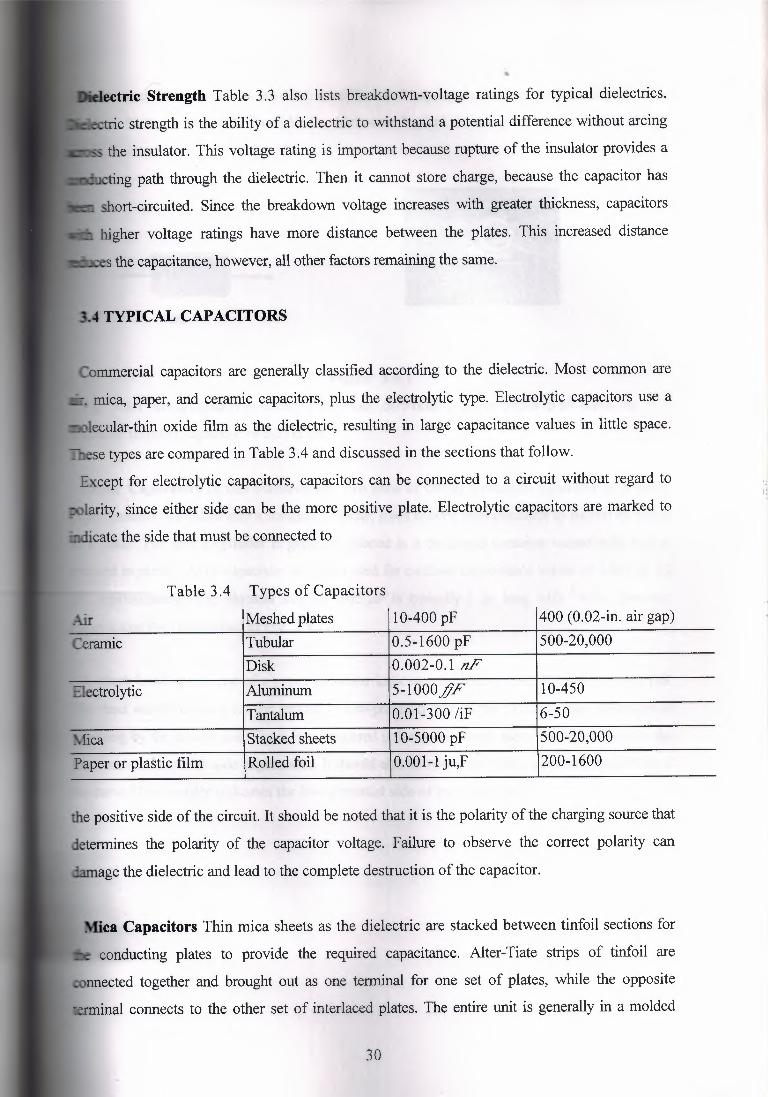
4 TYPICAL CAP A CITO RS
Commercial capacitors are generally classified according to the dielectric. Most common are
mica, paper, and ceramic capacitors, plus the electrolytic type. Electrolytic capacitors use a
lecular-thin oxide film as the dielectric, resulting in large capacitance values in little space.
e types are compared in Table 3.4 and discussed in the sections that follow.
Except for electrolytic capacitors, capacitors can be connected to a circuit without regard to
larity, since either side can be the more positive plate. Electrolytic capacitors are marked to
· '· cate the side that must be connected to
I' .
Table 3.4 Types of Capacitors
Air Meshed plates 10-400 pF 400 (0.02-in. air gap)
Ceramic Tubular 0.5-1600 pF 500-20,000 Disk 0.002-0.1 nF
Electrolytic Aluminum 5-1000.ffF 10-450 Tantalum 0.01-300 /iF 6-50
Mica \ Stacked sheets 10-5000 pF 500-20,000
Paper or plastic film I Rolled foil 0.001-1 ju,F 200-1600
the positive side of the circuit. It should be noted that it is the polarity of the charging source that
determines the polarity of the capacitor voltage. Failure to observe the correct polarity can
damage the dielectric and lead to the complete destruction of the capacitor.
lea Capacitors Thin mica sheets as the dielectric are stacked between tinfoil sections for
conducting plates to provide the required capacitance. Alter-Tiate strips of tinfoil are
nnected together and brought out as one terminal for one set of plates, while the opposite
lemlinal connects to the other set of interlaced plates. The entire unit is generally in a molded
30

Bakelite case. Mica capacitors are often used for small capacitance values of 50 to 500 pF; their
length is % in. or less with about Vs-in. thickness. Typical mica capacitors are shown in Fig.
3.4.1.
(a)
. - ..
Figure: 3.4.1
Fig. 3 .4.1 Mica capacitors about % in. wide, (a) Fixed C, color coded in pF units, (b)
Variable trimmer capacitor of 6 to 60 pF.
Paper Capacitors In this construction, two rolls of tinfoil conductor separated by a tissue
paper insulator are rolled into a compact cylinder. Each outside lead connects to its roll of tinfoil
as a plate. The entire cylinder is generally placed in a cardboard container coated with wax or
encased in plastic. Paper capacitors are often used for medium capacitance values of 0.001 to 1.0
,uF, approximately. The physical size for 0.05 µFis typically 1 in. long with 3 /4-in. diameter.
Paper capacitors are shown in Fig. 3.4.2.
! ~ • .. ..
A black band at one end of a paper capacitor indicates the lead connected to the outside foil.
This lead should be used for the ground or low-potential side of the circuit to take advantage of
shielding by the outside foil. There is no required polarity, however, since the capacitance is the
same no matter which side is grounded. It should also be noted that in the schematic symbol for C
the curved line usually indicates the low-potential side of the capacitor.
31

"'' ·. "'30 +-i()cr:
~ - IW /0
D
(b)
Figure:3.4.2
Fig. 3.4.2 Paper or plastic-film capacitors, (a) Tubular type 1 in. long. Capacitor C is
0.068s/u,F. (b) Encapsulated type with leads for printed-circuit board. Capacitor Cis 430 pF.
Plastic Capacitors Many capacitors of foil construction use a plastic film instead of tissue
paper. Two types are Teflon1 and Mylar1 plastic film. These feature very high insulation
resistance, of over 1000 MQ, low losses, and longer service life without voltage breakdown,
compared with paper capacitors. The plastic capacitors are available in sizes of 0.001 to 1.0 µ,F,
like paper capacitors.
Ceramic Capacitors The ceramic dielectric materials are made from earth fired under
extreme heat. By use of titanium dioxide, or several types of silicates, very high values of
dielectric constant At-can be obtained.
In the disk form, silver is fired onto both sides of the ceramic, to form the conductor plates. With
a.Ke value of 1200, the disk ceramics feature capacitance values up to 0.01 µFin much less space
than a paper capacitor.
For tubular ceramics, the hollow ceramic tube has a silver coating on the inside and outside
surfaces. With values of 1 to 500 pF, these capacitors have the same applications as mica
capacitors but are smaller. Typical ceramic capacitors are shown in Fig. 3.4.3.
32

Figure: 3.4.3
Fig. 3.4.3 Ceramic capacitors, (a) Disk type. Values from 33 pF to 0.02 µF. (b) Tubular
type. Values in pF units.
Chip Capacitors These are very small, typically Vi in. square or less with a ceramic
dielectric. Capacitance values are about 10 pF to 4 µF. The construction has alternate layers of
ceramic and a deposited conducting material.
Temperature Coefficient Ceramic capacitors are often used for temperature
compensation, to increase or decrease capacitance with a rise in temperature. The temperature
coefficient is given in parts per million (ppm) per degree.
Celsius, with a reference of 25°C. As an example, a negative 750 ppm unit is stated as N750. A
positive temperature coefficient of the same value would be stated as P750. Units that do not
change in capacitance are labeled NPO.
Variable Capacitors Figure 3.4b shows a variable air capacitor. In this construction, the
fixed metal plates connected together form the stator. The movable plates connected together on
the shaft form the rotor. Capacitance is varied by rotating the shaft to make the rotor plates mesh
with the stator plates. They do not touch, however, since air is the dielectric. Full mesh is
maximum capacitance. Moving the rotor completely out of mesh provides minimum capacitance.
A common application is the tuning capacitor in radio receivers. When you tune to different
stations, the capacitance varies as the rotor moves in or out of mesh. Combined with an
inductance, the variable capacitance then tunes the receiver to a different resonant frequency for
each station. Usually two or three capacitor sections are ganged on one common shaft.
33
Capacitance Tolerance Ceramic disk capacitors for general applications usually have a
tolerance of ±20 percent. Paper capacitors usually have a tolerance of ±10 percent. For closer
tolerances, mica or ceramic tubular capacitors are used. These have tolerance values of ±2 to 20
percent. Silver-plated mica capacitors are available with a tolerance of± 1 percent.
The tolerance may be less on the minus side to make sure there is enough capacitance,
particularly with electrolytic capacitors, which have a wide tolerance. For instance, a 20µF
electrolytic with a tolerance of-10 percent, +50 percent may have a capacitance of 18 to 30 µF.
However, the exact capacitance value is not critical in most applications of capacitors for filtering,
ac coupling, and bypassing.
Voltage Rating of Capacitors This rating specifies the maximum potential difference that
can be applied across the plates without puncturing the dielectric. Usually the voltage rating is for
temperatures up to about 60°C. Higher tempera-hires result in a lower voltage rating. Voltage
ratings for general-purpose paper, nuca, and ceramic capacitors are typically 200 to 500 V.
Ceramic capacitors with ratings of 1 to 5 kV are also available.
Electrolytic capacitors are commonly used in 25-, 150-, and 450-V ratings. In addition, 6- and
10-V electrolytic capacitors are often used in transistor circuits. For applications where a lower
voltage rating is permissible, more capacitance can be obtained in a smaller physical size.
The potential difference across the capacitor depends upon the applied voltage and is not
necessarily equal to the voltage rating. A voltage rating higher than the potential difference applied
across the capacitor provides a safety factor for long life in service. With electrolytic capacitors,
however, the actual capacitor voltage should be close to the rated voltage to produce the oxide
film that provides the specified capacitance.
The voltage ratings are for de voltage applied. The breakdown rating is lower for ac voltage
because of the internal heat produced by continuous charge and discharge.
Capacitor Applications In most electronic circuits, a capacitor has de voltage applied,
combined with a much smaller ac signal voltage. The usual function of the capacitor is to block the
de voltage but pass the ac signal voltage, by means of the charge and discharge current. These
applications include coupling, bypassing, and filtering for ac signal.
34

3.5 ELECTROLYTIC CAPACITORS
These capacitors are commonly used for C values ranging from 5 to 5000 /AF, because
electrolytics provide the most capacitance in the smallest space with least cost.
Construction Figure 3.5.1 shows the aluminum-foil type. The two aluminum electrodes are
in an electrolyte of borax, phosphate, or carbonate. Between the two aluminum strips, absorbent
gauze soaks up electrolyte to provide the required electrolysis that produces an oxide film. This
type is considered a wet electrolytic, but it can be mounted in any position.
When de voltage is applied to form the capacitance in manufacture, the electrolytic action
accumulates a molecular-thin layer of aluminum oxide at the junction between the positive
aluminum foil and the electrolyte. The oxide film is an insulator. As a result, capacitance is
formed between the positive aluminum electrode and the electrolyte in the gauze separator. The
negative aluminum electrode simply provides a connection to the electrolyte. Usually, the metal
can itself is the negative terminal of the capacitor, as shown in Fig. 3.5.lc.
:I :1
~lf!ifl f\lm
PO$t1v~~oc» (~m.ffl~j
(«)
Figure:3.5.1
Fig. 3.5.1 Construction of aluminum electrolytic capacitor. (tz)Intemal electrodes, [0)Foil
rolled into cartridge, (c) Zypical capacitor with multiple sections.
Because of the extremely thin dielectric film, very large Cvalues can be obtained. The area is
increased by using long strips of aluminum foil and gauze, which are rolled into a compact
cylinder with very high capacitance. For example, an electrolytic capacitor the same size as a 0.
35

Nonpolarized Electrolytics This type is available for applications in circuits without any
de polarizing voltage, as in the 60-Hz ac power line. One application is the starting capacitor for
ac motors. A nonpolarized electrolytic actually contains two capacitors, connected internally in
series-opposing polarity.
paper capacitor, but rated at 10 V breakdown, may have 1000 µF of capacitance or more.
•.. r voltage ratings, up to 450 V, are used, with typical Cvalues up to 5000 µF. The very
= C values have lower voltage ratings.
Polarity Electrolytic capacitors are used in circuits that have a combination of de voltage and
voltage. The de voltage maintains the required polarity across the electrolytic capacitor to form
oxide film. A common application is for electrolytic filter capacitors to eliminate 60-Hz ac
:pple in a de power supply. Another use is for audio coupling capacitors in transistor
plifiers. In both these applications, for filtering or coupling, electrolytics are needed for large
C with a low-frequency ac component, while the circuit has a de component for the required
.oltage polarity. Incidentally, the difference between filtering an ac component out or coupling it
· to a circuit is only a question of parallel or series connections. The filter capacitors for a power
supply are typically 40 to 400µF Audio capacitors are usually 5 to 10 µF.
' If the electrolytic is connected in opposite polarity, the reversed electrolysis forms gas in the
capacitor. It becomes hot and may explode. This is a possibility only with electrolytic capacitors.
Leakage Current The disadvantage of electrolytics, in addition to the required
polarization, is their relatively high leakage current, since the oxide film is not a perfect
insulator. Leakage current through the dielectric is about 0.1 to 0.5 mA/µF of capacitance for the
aluminum-foil type. As an example, a 1 OµF electrolytic capacitor can have a leakage current of 5
mA. For the opposite case, a mica capacitor has practically zero leakage current.
The problem with leakage current in a capacitor is that it allows part of the de component to be
coupled into the next circuit along with the ac component. However, electrolytics are generally
used fa low-resistance circuits where some leakage current is acceptable because of the small /R
drop.
36
~~----------11111111111111111111111111111111• •••

antalum Capacitors This is another form of electrolytic capacitor, using tantalum (Ta)
of aluminum. Titanium (Ti) is also used. Typical tantalum capacitors are shown in Fig .
. They feature:
ger C in a smaller size
Less leakage current
However, tantalum electrolytics cost more than the aluminum type. Methods of construction for
talum capacitors include the wet-foil type and a solid chip or slug. The solid tantalum is
essed in manufacture to have an oxide film as the dielectric. Referring back to Table 3.4, note
tantalum oxide has a dielectric constant of 25, compared with 7 for aluminum oxide.
- Figure:3.5.2
Fig. 3.5.2 Low-voltage electrolytic capacitors. These are tantalum type, with Cof 5 to 25
. (a) With axial leads, (b) Miniature type with radial leads for printed-circuit board.
· ght about !1 in. without leads.
CAPACITOR COLOR CODING
fica and tubular ceramic capacitors are color-coded to indicate their capacitance value. Since
· g is necessary only for very small sizes, the color-coded capacitance value is always in pF
. The colors used are the same as for resistor coding, from black for O up to white for 9.
capacitors generally use the six-dot system shown in Fig. 3.6.1. Read the top row first from
right, then the bottom row, in reverse order right to left. White for the first dot indicates the
· EIA coding, but the capacitance value is read from the next three dots. As an example, if the
are red, green, and brown for dots 2, 3, and 4, the capacitance is 250 pF. If the first dot is
37
" ..

silver, it indicates a paper capacitor, but the capacitance is still read from dots 2, 3, and 4. Dot 5
specifies tolerance, while dot 6 gives the EIA class. There are seven classes from A to G,
specifying temperature coefficient, leakage resistance, and additional variable factors. Appendix
B has more detailed information on the tolerance and class coding.
For tubular ceramic capacitors, the system shown in Fig. 3.6.2 is used with color dots or bands.
The wide color band specifying temperature coefficient indicates the left end, which is the side
nnected to the inner electrode. Capacitance is read from the next three colors, in either dots or
ipes. For instance, brown, black and brown for bands or dots 2, 3, and 4 means 100 pF.
WhRe I Digit
2 ta
6f 5 t 4
Class I Multiplier
Tolerance
Figure3.6.l
. 3.6.1 Six-dot color code for mica capacitors.
Tolerance
Figure:3.6.2
.6.2 Color code for ceramic tubular capacitors
ar ceramic capacitors, the system shown in Fig. 3.6.2 is used with color dots or bands.
color band specifying temperature coefficient indicates the left end, which is the side
38

connected to the inner electrode. Capacitance is read from the next three colors, in either dots or
stripes. For instance, brown, black and brown for bands or dots 2, 3, and 4 means 100 pF.
Gray and white are used as decimal multipliers for very small values, with gray for 0.01 and
white for 0.1. For instance, green, black, and white in dots 2, 3, and 4 means 50 x 0.1, or 5 pF.
The color codes for tolerance and temperature coefficient of ceramic capacitors are listed in
App. B.
In reading the color-coded capacitance value, keep in mind that mica capacitors generally range
from 10 to 5000 pF. The small tubular ceramic capacitors are usually 0.5 to 1000 pF. With paper
and ceramic disc capacitors, the capacitance and voltage rating is generally printed on the case.
Where no voltage rating is specified, it is usually about 200 to 600 V. Electrolytic capacitors have
capacitance, voltage rating, and polarity printed on the case.
3.7 PARALLEL CAPACITANCES
Connecting capacitances in parallel is equivalent to adding the plate areas. Therefore, the total
itance is the sum of the individual capacitances. As illustrated in Fig. 3.7,
l Cr
r c,-c,+c;
- 2 ,.F Fig: 3. 7 Capacitances in parelell
OµF capacitor in parallel with a 5-/uF capacitor, for example, provides a 15µF capacitance for
.-allel combination. The voltage is the same across the parallel capacitors. Note that adding
:l capacitances is opposite to the case of inductances in parallel, and resistances in
I.
39

SERIES CAPACITANCES
Connecting capacitances in series is equivalent to increasing the thickness of the dielectric.
fore, the combined capacitance is less than the smallest individual value. As shown in
.8.1 , the combined equivalent capacitance is calculated by the reciprocal formula
l 1 - =- -- + ......•. + · ·· + ere. 'r C1 Cz
1 1 1 -~-+- Cr C, Cl Cr m 0.5 µ.F
Fig. 3.8.1 Capacitances in series.
_; of the short-cut calculations for the reciprocal formula apply. For example, the combined
itance of two equal capacitances of 10 /uF in series is 5/tiF.
l:'lplcitors are used in series to provide a higher working voltage rating for the combination. For
IIIIIIDCe, each of three equal capacitances in series has one-third the applied voltage.
· ion of Voltage across Unequal Capacitances In series, the voltage across each Cis
lmsely proportional to its capacitance, as illustrated in Fig. 3.8.2. The smaller capacitance has
ltllrger proportion of the applied voltage. The reason is that the series capacitances all have the
ge because they are in one current path.
equal charge, a smaller capacitance has a greater potential difference.
Fig. 3.8.2 With series capacitors, the smaller Chas more voltage for the same charge
40
We can consider the amount of charge in the series capacitors in Fig. 3.8.2. Let the charging
current-be 600 juA flowing for 1 s. The charge {]equals 7 X tor 600 /u,C. Both Ci and C,have {2 equal to 600 lu,C, as they are in the same series path for charging current.
Although the charge is the same in Cl and C2, the-y have different voltages because of different
capacitance values. For each capacitor//= {2/C For the two capacitors in Fig. 3.8.2, then:
Q _ 600 µ.C = 600V V, = c;- l µ.F
Q _ 600 µ..F = 300 V V2 "" c2 - 2 µ.F
Charging Current for Series Capacitances The charging current is the same in all parts
if the series path, including the junction between C1 and C2, even though this point is separated
the source voltage by two insulators. At the junction, the current is the resultant of electrons
Iled by the negative plate of C2 and attracted by the positive plate of C1 The amount of
nt in the circuit is determined by the equivalent capacitance of Ci and C2 in series. In
.8.2, the equivalent capacitance is 2/3 µF.
STRAY CAPACITIVE AND INDUCTIVE EFFECTS
two important characteristics can be evident in all circuits with all types of components.
itor has a small amount of inductance in the conductors. A coil has some capacitance
windings. A resistor has a small amount of inductance and capacitance. After all, a
.-,-....,.ce physically is simply an insulator between two conductors having a difference of
An inductance is basically just a conductor carrying current.
1y, though, these stray effects are usually quite small, compared with the concentrated or
values of capacitance and inductance. Typical values of stray capacitance may be 1 to 10
while stray inductance is usually a fraction of 1 µH. For very high radio frequencies,
, when small values of .L and C must be used, the stray effects become important. As
example, any wire cable has capacitance between the conductors.
· cal case of problems caused by stray L and C is the example of a long cable used for RF
If the cable is rolled in a coil to save space, a serious change in the electrical
41

characteristics of the line will take place. Specifically, for twin-lead or coaxial cable feeding the
antenna input to a television receiver, the line should not be coiled, as the added L or C can affect
the signal. Any excess line should be cut off, leaving just the little slack that may be needed.
This precaution is not so important with audio cables.
Stray Circuit Capacitance The wiring and the components in a circuit have capacitance to
.e metal chassis. This stray capacitance Cs is typically 5 to 10 pF. To reduce c:;, the wiring d be short, with the leads and components placed high off the chassis. Sometimes, for very
frequencies, the stray capacitance is included as part of the circuit design. Then changing
placement of components or wiring affects the circuit operation. Such critical lead dress is
y specified in the manufacturer's service notes .
..,.. ••• ge Resistance of a Capacitor Consider a capacitor charged by a de voltage source.
the charging voltage is removed, a perfect capacitor would keep its charge indefinitely.
~ there is no perfect insulator, after a long period of time, however, the charge will be
~GULA.,d by a small leakage current through the dielectric and across the insulated case I
~n terminals. For paper, ceramic, and mica capacitors, though, the leakage current is very
or, inversely, the leakage resistance is very high. As shown in Fig. 3.9.1, the leakage
I -wmce R1 is indicated by a high resistance in parallel with the capacitance C. For paper,
-.nic, or mica capacitors .R/is 100 Mn or more. However, electrolytic capacitors may have
·!IAr-kage resistance of 0.5 Mn or less.
C
Fl, &
100 MO
Rd"' o.sn
Figure:3.9.1
Equivalent circuit of a capacitor; R1 is leakage resistance and R, is absorption
D rntion Losses in Capacitors With ac voltage applied to a capacitor, the continuous
discharge, and reverse charging action cannot be followed instantaneously in the
ic. This corresponds to hysteresis in magnetic materials. With a high-frequency charging
42

voltage applied to the capacitor, there may be a difference between the amount of ac voltage '
applied and the ac voltage stored in the dielectric. The difference can be considered absoption
loss in the dielectric. With higher frequencies, the losses increase. In Fig. 3.9.1, the small value
of 0.50 for Rd indicates a typical value for paper capacitors. For ceramic and mica capacitors,
the dielectric losses are even smaller. These losses need not be considered for electrolytic
capacitors because they are generally not used for radio frequencies.
Power Factor of a Capacitor The quality of a capacitor hi terms of minimum loss is often
indicated by its power factor. The lower the numerical value of the power factor, the better is the
quality of the capacitor. Since the losses are in the dielectric, the power factor of the capacitor is
essentially the power factor of the dielectric, independent of capacitance value or voltage rating.
t radio frequencies, approximate values of power factor are 0.000 for air or vacuum, 0.0004
:or mica, about 0.01 for paper, and 0.0001 to 0.03 for ceramics.
The reciprocal of the power factor can be considered the {?of the capacitor, similar to the idea
g of a coil. For instance, a power factor of 0.001 corresponds to a f2 of 1000. A higher g fore means better quality for the capacitor.
Inductance of a Capacitor Capacitors with a coiled construction, particularly paper and
olytic capacitors, have some internal inductance. The larger the capacitor, the greater is its
· es inductance. Mica and ceramic capacitors have very little inductance, however, which is
iy they are generally used for radio frequencies.
use above audio frequencies, the rolled-foil type of capacitor must have a noninductive
--,d-n1ction. This means the start and finish of the foil winding must not be the terminals of the
itor. Instead, the foil windings are offset. Then one terminal can contact all layers of one
at one edge, while the opposite edge of the other foil contacts the second terminal. Most
-foil capacitors, including the paper and Mylar types, are constructed this way.
ibuted Capacitance of a Coil As illustrated in Fig. 3.9.2, a coil has distributed
itance Cd between turns. Note that each tum is a conductor separated from the next tum by
lator, which is the definition of capacitance. Furthermore, the potential of each tum is
nt from the next, providing part of the total voltage as a potential difference to charge Cat
result then is the equivalent circuit shown for an RF coil. The L is the inductance and A'e its
43
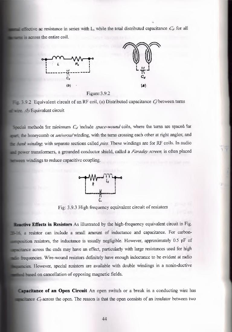
L R. l I I I II I ~-------,~-------~ '\
ective ac resistance in series with L, while the total distributed capacitance ~ for all
· across the entire coil.
c<I
I II I L -,t- .J . '
Cd
(b} (a)
Figure:3 .9 .2
Equivalent circuit of an RF coil, (a) Distributed capacitance (?between turns
~li:U methods for minimum C,1. include space-wound coils, wnere tne turns are spacea iar
the honeycomb or universalwinding, with the turns crossing each other at right angles; and
/Jank winding, with separate sections called p/es. These windings are for RF coils. In audio
wer transformers, a grounded conductor shield, called a Faraday screen, is often placed
...•....•..• It ~ Ls 1
I
~~---_J C.
Fig: 3.9.3 High frequency equivalent circuit ofresistors
:five Effects in Resistors As illustrated by the high-frequency equivalent circuit in Fig.
a resistor can include a small amount of inductance and capacitance. For carbon
ition resistors, the inductance is usually negligible. However, approximately 0.5 pF of
pcitance across the ends may have an effect, particularly with large resistances used for high
frequencies. Wire-wound resistors definitely have enough inductance to be evident at radio
ies, However, special resistors are available with double windings in a nonin-ductive
d on cancellation of opposing magnetic fields.
citance of an Open Circuit An open switch or a break in a conducting wire has
ce Co across the open. The reason is that the open consists of an insulator between two
44
:tors. With a voltage source in the circuit, C0charges to the applied voltage. Because of the
Ca in the order of picofarads, the capacitance charges to the source voltage in a short time.
· charging of Co is the reason why an open series circuit has the applied voltage across the
terminals. After a momentary flow of charging current, Co charges to the applied voltage
ores the charge needed to maintain this voltage.
Bow to read a capacitor
the printing from the capacitor has the complete, obvious value on it, like 3,300 uF, you
home free and don't have to think any more. That is typical only for large valued
citors with lots of space for printing. Some tantalum capacitors have this as well, though,
they aren't so big. In general, it helps to know what type of capacitor you have so that you
at least figure out about how large the value should be.
But down to business.
Typically, the numbers are in a mn(nnn) x 10"'3 format where you have some group of
lilnificant digits followed by a single digit multiplier (i.e. 332 corresponds to 33 x 1 Q!'2 or
'). BUT, they don't tell you what the base value is. ALMOST ALWAYS, this base value
1F. Why? Well, nF doesn't sound cool, I guess and by the time something becomes uF or
sized, you can just print the whole number on the capacitor. Some capacitors are always
to be exceptions to this rule, so you need to pay attention. For example, some of the
capacitors are marked .047; what is .047? Well, .047 is .047uF. Others in the box are
ed 473, which means 47 x lQ/''3 pF or 47nF or .047uF, the normal designation. Also, I've
into some silver mica caps that were marked 10 (as in lOpF, not 1 x 101'0 or 1 pF). It
to know what capacitance value to expect based upon the physical size of the capacitor
e cases.
45

Table of ~\)ical ranges of values for different ~es of capacitors:
Type of capacitor\\Typical range of values Working Voltage Rangel
!Silver Mica J1
\ I =: I
!Single Layer lllpF - 47nF IJsov - 6KV I JMultilayer or Stacked: I
__ J JcoG/NPO lllOpF - 27nF Jjsov .zoov ;
I [X7R J~~ - 580nF Jjsov .zoov I Jzsu l~ - ~.2uF IJsov, 100v I I/Metallized Film: J //Polyester IJlnF - 15uF IJsov - 1 soov I
J
//Polycarbonate //IOOpF - 15uF //63V - 1 OOOV I " ropylene ljIOOpF - lOuF Jj63V - 2000V
\~~~rene J\10pF-47nF ~E_V -630V 1
~\Metallised paper liinF - 0.47uF l!250VAC I
i J
;(Electrolytics:
to 450V
Capacitor codes
s you really like to know how to read all those different codes. Not to worry, it is not
cult as it appears to be. Except for the electrolytic and large types of capacitors, which
have the value printed on them like 470µF 25V or something, most of the smaller
have two or three numbers printed on them, some with one or two letters added to that
Check out the little table below.
46

Capacitor Value Codes
3rd Digit Multiplier Letter Tolerance
0 1 D O • .":i pF 1 10 F 1% 2 10D G 2% a 1,000 H 3% 4 10,000 J 5% .s mu.nen K 10 '¥11 fi,? Not U5ed M ,, 20 'ttl 8 .ni p +100,-0% 9 .1 t: +80, -20 %
Fig: 3.11.1
look at Fig.3 .11.1 and Fig. 3 .11.2. As you can see it all looks very simple. If a
is marked like this 105, it just means l O+Szeros = l O + 00000 = l .000.000pF =
= 1 µF. And that's exactly the way you write it too. Value is in pF (Picofarads). The
added to the value is the tolerance and in some cases a second letter is the temperature
- t mostly only used in military applications, so basically industrial stuff.
example, it you have a ceramic capacitor with 474J printed on it it means:
s = 470000 = 470.000pF, J=5% tolerance. (470.000pF = 470nF = 0.47µF) Pretty
huh? The only major thing to get used to is to recognize if the code is µF nF, or pF.
capacitors may just have 0.1 or 0.01 printed on them. If so, this means a value in µF.
means just 0.1 µF. If you want this value in nanoFarads just move the comma three
the right which makes it 1 OOnF.
average hobbyist uses only a couple types like the common electrolytic and ceramic
and depending on the application, a more temperature stable type like metal-film or
ene.
Fig : 3.11.2
47

4. DIODES
SEMICONDUCTOR DIODES
e is essentially a PN junction. The standard symbol is an arrow to indicate the direction of
•u:nrrent and a bar, as shown in Fig. 4.1.1. The arrow is at the anode, which must be positive
twient flow, while the bar is the cathode. Conventional current is in the direction of the arrow
n flow is the opposite way, against the arrow. The practical use of diodes is to serve as a
• valve. Current can flow only when positive voltage at the anode with respect to cathode,
forward voltage. With the reverse polarity, no forward current can flow. This feature is
for the general use of the diode as a rectifier to change ac input to de output.
- 'l
small semiconductor diodes are shown in Fig. 4.1.1. In Fig. 4.1.1 la, the symbol is on the
to indicate anode and cathode. For the diode in Fig. 28-1 /b, the colored band at one end
llicates the cathode side. Some diodes may have a + sign at the cathode end to show this is positive de output can be obtained in a rectifier circuit. Any mark at one end indicates the
.e side. The cathode has positive de output when the ac input is applied to the anode.
Cathode :tr~~· Anoele
(a) (b) (C)
Figure:4.1.1
Semiconductor diode rectifiers. Length is about Y-iin. without leads, (a) Silicon
iode with current rating of 1 A. the arrow shows the direction of the hole current, (b)
detector diode. The cathode end has a dark band, ( c) Schematic symbol for diode.
48

Type Numbers The numbering system for diodes uses the letter N for semiconductors, the
fix 1 before the N and numbers after the ~ for individual types. The 1 means one junction.
an example, the 1N3196 is a popular silicon diode. The IN indicates a semiconductor diode,
·· e the 3196 specifies the individual characteristics, which are listed in semiconductor
books, specification sheets, and application notes. There is no special indication for Si or Ge,
practically all rectifier diodes are made of silicon. In schematic diagrams, diodes are usually
D, CR, or X and Y. The CR stands for crystal rectifier.
I lifier Packaging The plastic package shown in Fig. 4.1.1 is very common with
~ for currents of about 1 A. Even smaller diodes can be used for less current. Two other
of rectifiers are shown in Fig. 4.1.2. The metal can in Fig. 4.1.2a is called "top-hat" style.
type in Fig. 4.1.2b uses a stud mount that screws directly into a metal mounting for the
e connection. Note the diode symbols printed directly on the unit to indicate the anode and
.e terminals. The stud mount types generally have high current ratings.
<•l (bl
Figure:4.1.2
Rectifier packages, (a) "Top-hat" style. Height is 3/8 in. without leads, (b)
rectifier for stud mounting. Height without stud is //2in.
Rectifiers This type of power supply is used very often, even though it requires four
Connections for the bridge are shown in Fig. 4.1.3a, while typical packages are in Fig.
c. Note that the bridge has four terminals. Two are connections for the ac input and
{b)
•. oo C><"\,'loilll
Figure:4.1.3
49

Fig. 4.1.3 The bridge rectifier, ( a) Sche our diodes as a full-wave bridge, (b)
Typical package. Length is 3 /4 in. ( c) Heavy-duty package for mounting on heat sink. Size is 1
in. square.
Rectifier Ratings The two most important ratings are for maximum forward current Ip and
maximum peak inverse voltage (PIV). Ratings for maximum ~an be a fraction of one ampere
up to 25 A or more. The PIV rating for popular diodes is typically about 1000 V. The peak
inverse voltage is the value that can be used across the diode in reverse polarity, negative at the
anode, without disrupting the electrical characteristics of the junction. The PIV rating must be at
t double the value of the de voltage output. The reason is that the de output and ac input are
series-aiding polarity across the diode when the anode. is negative.
4.2 SPECIAL-PURPOSE DIODES
r.
A semiconductor diode is just a PN junction. Since forward current flows only one way, the
use is rectification. Besides having polarity, however, the PN junction has additional
perties that are useful. Popular applications include:
'I
.l Capacitive diode or varactor. With reverse bias, the diode junction has capacitance that
be varied by the de voltage.
Yoltage-rl!ference diode. The reverse breakdown voltage provides a steady de value for
Tunnel diode. This type has a negative resistance characteristic.
'hotoelectric modes. Semiconductors have characteristics related to light.
internal .Rcan be changed by light input. Also, the light-emitting diode (LED) can emit
these applications depend on the unique features of semiconductor materials. Schematic
bols for these special-purpose diodes are shown in Fig. 4.2.1
50

Figure:4.2.1
Schematic symbols for popular types of diodes. Note that the photodi-ode in
light input to vary its ..R, whereas the LED in (/) generates light output.
etor Diodes This type is also called a varicap or capacitive diode. With reverse voltage,
· er voltage enables the junction to serve as a capacitance because of the separated charges
depletion zone. The C values are in the picofarad (10-12 F) range. Most important, the
of junction capacitance can be controlled by varying the reverse voltage.
outline drawings of a varactor are illustrated in Fig. 4.2.3a. A mark at one end indicates
. The schematic symbol is in Fig. 4.2.3b. The graph in Fig. 4.2.4 shows that Cv of
can be varied from 400 to 20 pF, with reverse voltages of 3 to 18 V. The reverse
.tive at the anode of the varactor. Its C decreases with more reverse voltage.
'i
circuit diagram in Fig. 4.2.5 on the next page illustrates how a varactor provides electronic
by varying the frequency of the oscillator gl. The LC tuned circuit determines the
.•. ator frequency. Across the tuned circuit, the varactor provides c;, as part of the capacitance determines the resonant frequency. When c;, is varied by a de control voltage applied as
bias, the oscillator is tuned to different frequencies determined by the capacitive diode.
T 1/2 in.
_L
K
f A
(a) (b)
. 4.2.2 The capacitive diode or varactor. (a) Outline, (b) Schematic symbol.
51

0 3 6 9 12 15 18
Reverse voltage, VR
Fig. 4.2.3 Operating characteristics of varactor with reverse voltage applied.
er Diodes These are voltage-reference diodes. They are named after C. A. Zener,
analyzed the voltage breakdown of insulators. Zener diodes are designed for a specific
breakdown voltage, typically 3 to 100 V. Series diodes can be used for a higher rating. At
down value, the reverse thin mica washer. Both sides are coated with silicone grease for
ipation to the chassis.
52

F=AIFICHILC 81iiiMICCNOUCTOR•
1 N4001 -1 N4007
Features • Low forward vcHage crop.
• High surge (urent Cfl,al:ility,
D0-41 COi.OR llANO £:C>t~OTTS C".All!DO[
General Purpose Rectifiers
Absolute Maximum Ratings* T,•25'Cunieo,cth•M••notod
Symbol Parameter Value I Units 4001 I 4002 I 4003 I 4004 I 400s I 400s I 4001
\IRRJ,I Peet Repetilive Reverse Voltage 50 I 100 I 200 I 400 I 600 I 800 11000 I V l,(A'I) Averaqe Recnfisd Forward Current
im · lead length@ T, = 75'C 1.0 I A
Non-repetitive Peak For.vard Surge Current
8.3 ms Sinqle Half-SinB-Wave 30 I A
T,~ Storage Temperature Range -55 to +175 I 'C
T, Opernting JuncUon Temperaurs -ss to+ 175 I -c . TheH rolirgs ere limmng ·,slue& :Jbovewhich lh~ se,~·i0:0bi~l)• cf any semioonductor cki~·be mo~· he impoked.
Thermal Characteristics Symbol I Parameter Value Units
F'o I Power Di~sipntion R.,.~ I Therm::, Resistance, Juncti;)l to Arnbent 50
Electrical Characteristics T, •25'Cunlmo!htroiHno\eo
Symbol I Parameter Device I Units 4001 l 4002 I 4003 I 4004 I 4005 I 4006 I 4007
V, I Forv,··ard Voltage@ 1.0 ,A, 1~ I V I, I Maximum Full Load Reverse Cufreri(Full
Cycle T, = 75°C 30 I uA
I" I Reverse Current@ rated \IR TA= 15"C T,= icoc
s.O I uA 500 pA
C, I Total Cap.1;citance V" = 4 0 V. f = 1.0 ldHz
-15___ I pF
{'200) J:alrotllld SC<111k:ou1uctm Corp:rnUon 1Hffl1MN4001. Rm. Cl
53
..• z ,l:i,, 0 C ..• I ..• z ,l:i,, C C ""'

General Purpose Rectifiers (continued)
Typical Characteristics
Forward current Denning Curve 1.6 ,--,,-..---,--r--.--.-- .•......• -.,
« 1.4 t--t---t-+-+--4-+--l--l_J i:' 1.2 i-+-;-+-+-+--+-1-..!-.....l ~ ,,-+-,f-+..J--l---t-1--...L_j B O.B SltlGLE PKASE Cl HALflo\;\\'E. !;l! o.s mil ?; REstSHJE OR ~ 0.4 -~~.~~~~l~~~' -,1---1-_;lll.--
o.2 LEN<'.'THS
00';-;!::--"'7:"--:!::_JL_L__L~l,,.__l__J 20 40 so so 100 120 140 1Go 100
AMBIENT TEMPERATURE ("CJ
Non-Repetitive Surge Curre.nt
" "'i-,. ~ r-, •.•...
.• 30 Q.
5 'z 24 "' "' "' a is ~ ~ 12 0
I •.•. 0 1 2 4 6 S 10 20 40 GO 100
NUMBER OF CYCLES AT GOHz
Forward Characteristics 20 10
I I I I I .Jt- I
. ,_ . I I /I I I I I
- ./1 I I I I I i.::~;~;dth.= JCi¥ ~
I . 2%DulyC-ydt! = , I I I I I I
...•. z ~ 0 ...•. I ...•. z ~ 0 0 ....•
'\
g > % w ex ~ (,)' 0.4 0 ; 0.2
i:: 0.1
i? 0.04 002 O.o1
0.6 0.8 1 1.2 FORWARD VOLTAGE tVJ
1.4
Reverse Characteristics
o.o1------~~~~~~~~- o 20 40 60 80 100 120 140 RATED PEAK REVERSE VOLTAGE('"•)
1N!'JL'1··1N4LX!l, Hi!IY. C1
54

5. CD4001 BC OF GATE
ER: 5
CD4001BC and CD4011BC quad gates are monolithic complementary MOS (CMOS)
.ted circuits constructed with N- and P-channel enhancement mode transistors. They
equal source and sink current capabilities and conform to standard B series output drive.
vices also have buffered outputs which improve transfer characteristics by providing
· gh gain. All inputs are protected against static discharge with diyotes to VDD and
· power TTL: Fan out of 2 driving 74L compatibility: or 1 driving 74LS
-10V-15V parametric ratings
._-.,mmetrical output characteristics
_ •.••• timum input leakage 1 µA at 15V over full temperature range
Package Number Package Description M14A 14-Lead Small Outline Integrated Circuit (SOie), JEDEC MS-(l'l2, 0.150" Narrow M14D ·14-Lead Small Outttne Package (SOP), EIAJ TYPE II, 5.3mm Wide N14A 14-Lead Plastic Dual-ln-Une Package (PDIP), JEDEC MS-001, 0.30011 Wide M14A 14-Lead Small oumne Integrated Circuit (SOIC), JEDEC MS-012, 0.150l' Narrow N14A 14-Lead Plastic Dual-In-Line Package {PDIP), JEDEC MS-001, 0.300" Wide
55

ection Diagrams
. gnments for DIP, SOIC and SOP IBC
6 7 I
V;s Top View
Schematic Diagrams
Voo
. 2 {6, I, 13)
2(6,$, 13.!
Pin Assignments for DIP and SOIC CD4001BC
Top View
CD4001BC lioo
1 I~ of device shown
J=A+B Logical "I'= HIGH Logical "!? = LOW AlHnputs protected by standard CMOS protection c:rcu~ .
CD4011BC Voo
114 of device shown
J=A•B logical "Y = HIGH
logical •o· = LO'lv All inputs protected by standard
CMOS prolectioo cirwlt.
56

5. 7 Absolute Maximum Ratings
Voltage at any Pin Po1Ner rnssipaUon (P0)
Dual!-ln-line small outline
V:0o Range storage Temperature ,(Ts) lead Temperature (TL)
{Soldering, to seconds)
5.8Recommended Operating Conditions
~ting Temperature Range 00'\'oC, CD,4t\'\'\'oC
DC Electrical Characteristics
-0.5V to Ve:) +0.5V
700mW 500mW
-D.5 Voe to +18 Voe -659C to + 150°C
26D°C
3 Voe to 1,5 Voe
Panmeter Cond'itions Min Max Min Typ
-55"C +25°C +125,¢C I Units
Max Min Max
0.2.5 7~5
0.50 t5 I ~LA
·1.0 3:1)
0.0.5 ,0.05·
D.05 ,0.05? I V
!J.05 ,0.05
Quiescent Dev.ice V:c/D = 5V,. V1N = 'Voo or Vs;:;, Voo= 1DV. V1t,i= V00,crVss \•bo= 15V. V1t,i= v00 crVss
Current
0.2.5 0.004 0.005
O.OD6 Cl.5
r.e _OV~Level OU1pUt Voltage 0.05
Vc,o=5V v,c,o = rev 1101,< 1 llA V,DD= 15V
'-l:oo=5V V00 = mv 11·o1..: 1 ILA \!:oo= 15'<1
0.05 D ,0
0 !J.05 ..;.Q5 9.Q5
V
4.95 9Jl5
14.9'5
4:Q,5 QJH5 "\4.95
\J•oo•=!N, \/c,=4.W \J\DD ·= \I,\/, \JO= '>i .Cl\J
''\Do= 15\/. \JO= i3.o,\J
\.'5 '\.5 ~.Q
4.0
'\J
4.0 V,c,o=5V, Vo=O,o,V V,c,o = rnv. v O = '1 .av \Joe= 'fi'-J, \Io='"\ .f:N \t,Dt:,='5\i,\Jo=OA\J \/DD= 1 DV, Vo = ,0,.§V
V,c,o'= 15V, Vo= '1.'5\/
3.5 7.0
\'Ul C.1!4 ·1.6
4.2
1.3
3.4
'2..2-5· mA
8.8 2.4
Vc,o= rnv. v0 =ll'.5'J V:o.D = 15V, Vo = l3.5V
~;i.~.i; -1.6<
-4.2 -'LS I -2'.2'5 -3.,4 -KB,
mA -2.4
V:c,o= 15V, V1t-1= OV V1:,o•= 15V, V1t,i= 15V
-1.,0,
'li.0
-'{UO 0.1
-10 1,0.-5
-{UO D.'1,0,
57

5.10 AC Electrical Characteristics
Symbol Para met& Units
1?'.HL J Propagation Delay Time, HIGH-to-LOW Level
Conditions Typ !M!ax
VDr;.=5\/ tW 250
VDD= 10:V 50 -ea Voo= 15\f 35 JO,
Voo=W '11() 250
vD'D= 10v 50 ·100
Voo= 15\l 35 JO
Voo=fN go 200
\/ciu= 10\J 50 100
Voo= 15V 40 80
Any!n·pu1 0 i'.5
I Any Gate. 14
1?1.t, J Propagation Delay Time, LOW-to-HIGH Level
tniL, tmi I Transitionlime
Power Dissipation Capa.oity
ns
ns
ns
pF
pF
11 AC Electrical Characteristics
Parameter Un ifs
Propagation Delay,
HIGH-to-W1N Le•iel
Conditions Typ Max
v00=5V 120 250
Voo = '1i0\/ 50 100
v00=·15V l5 70
Voo = 5\1 &5 250
Voo='lOV 4{I 1{)0
Voo='t5V w 70
v00=5V ~o 20'1l
v00 = 10v 50 mo v00,d5V 4{1 8;0
An~· l:np,ut 5 7.5
Any Gate '14
Propag,alion, Delay,
LOW-lo-lHIGH Level
• tnH I Transition Time
Average Input Gapacilanc,;.
PowerDissipalion Capacily
ns
ns
ns
pF pF
58

Typical Performance Characteristics
Typica.t Transfer Cha.racteristics
20 C040iH:! TA:: 25oC
-4 Yoo.
~ >'1 v~! ID--
15
10
s
0 0 lO 15
v1- IN PITT VOLTAGE {V) ONE INPUT ONLY
Typical Transfer Characteristics 20 1 --r--i-~:.._ ... I C0400tB I
15 Voo•15V '!A;251>C
'{ I I ,, n .. ~ .. ·~· .. s 1~,=~. -··-· - ... -~ .. :.:.r· ·
! ~·lo--
QL-_._..., __ •.... .._ __ ...L~__J 0 10 15
V1- INPVT ~'QLTAGE (V) ONE INP\JT ONLY
59
Typical Transfer Characteristics 20 ·--r--,-~~- 1 Cll401l B I
1S 1'w·"'I I 1 'T'"' I ..,~~·}
.. 1
·-·-•·-- V5.s· •
•! I I I ~-- (-1 S~;;5Y
5 10 15
V1 - ~PUT VOLlAGC (V) BOTH INPUTS

Typical Tran sf er Characteristics
20 ' i co~o,ne T.1, = ZS~(,
f '1!'['.{1
'1"~~·1(ty'I I I ~ .. ', •... · 10~ · , •
v, . -~-i y .
s F-t-f+I ,.. : ~ -·
Yoo"~.,. I o I I ·Ill. I I 0 5
V1- !Nf'tll 'iotUGE (V) E!Offl !NF'ITTS
D 11 1ri'.l
4ot -~D4011B T,i,=25:'C CL •H pf
lllll
lOQ t--
u 0 ,10 15
lion - :,i;Pet '{ VOUAG!E. Hfl
60
i)il h 0 l'(Xl,
I zoo l'.f'-!),4-:oo""",i"!!'s----r--,---·-- T~= i~
,jp I
0

ical Performance Characteristics
oL....~-1.~~-'-~~---~-' 0 25 75 100
. .5
lr:t.,=20 ns, TA:: 25°C ,
COt0018 \ I C0401Hl
' (* AppllcAtlon 1'1¢{e AN .,.JJO
I I\ Propaga)kla Oefey)
i\. '
I ~
I
• tJ
0.5
0 0 2 4 6 8 10 12. 14 l6 18 20
Voo- POWER SUPPLY (V)
6
- ., C ....•• 190 ICDAOOI B l10 CD-401 IB
150
:~I tffi 30
j 1gl ~1 c:=±==1 ·· o 25 50 rs 100
38 C04001B 1 ' ~
34 _@40U ~J- - -l- .. 1
, 30 · v00:: 15V 26 I
22~-A--l--!--!--l--+-+-+-I
18 '1.f
'im-1.,~svl 1111 I o 2 .4 e e io 12 1,4 16 re 2.0
VourM

••...... < 2 e - I-
6 % uJ 10 a:: °'" ::::> 14 <;.) I.I.I 18 u ci:· =:-i 22 0 Vl ...J 24 < ~ 28 ~ I :i:: ..9
2-0 1B l 6 14 12 10 8 6. 4 2 0
Ycc-V 01.11 (v)
5.15 Physical Dimensions inches (millimeters) unless otherwise noted
1
-c O 335-!1.3U . ['8. !l,OO-Ul6J-----,
,----· 14 rs 'IZ 11 · I
i 19 A 8 8 ~ ~ ~j I o.ns-0_244 f!i.191-6.1gsi I -- .. n ! - I 30·
""',,,,,;11/1''-..._j r'f P ,, LM~NO. 1 / ,·· t; >··
!Ot~n 1 i e ~ § 6 § ; ///./ \ 2 . .. • e. •
_ o.,so-Q.m .1,._ 1 tUlO-t9B11) •:::'.::i ds·l .:...I_. __ ..,I !~~~: , t .. } i LJl]_ . • ~--= ! ·j1 t D.008-0.010 • i O.Olti -0.~ 1uo3-o.2:sM ··_ 1--10.40&-1.mi m ~l WllS ~ 'fYP ALL m~s - (!UD2) . .
Alt l.fAnlPS
G.053~0.~ p .346 - 1.753}
1 O.!Wt-0.010 (OJtZ- 0.2$4)
t m.nNG _.,., PWE t t
0.014 lU~l
-Lead Small Outline Integrated Circuit (SOIC), JEDEC MS..a012, 0.150" Narrow Package
3umberM14A
62

Dimensions inches (millimeters) unless otherwise noted (Continued)
5.3.z0,1 j ;6-- j
'' II' ._l i I I I I · I I , ,
DIMENSIONS ARE IN MILLIMETERS
ll«)TES; CONFORMS TO E!AJ EDR-7320 REGISTRATION, ESTAl:3LISHED IN DECEMBER, 1998. on . .1ENS10~S ARE IN MlllJMETERS. DIMENSIONS ABE EXCLUSlVE OF BURRS, MQlD FLASH, AND TIE BAR EXTRUSIONS.
M14DRe\l81
OOiOO 14 13 I 9 a 1
I 5.01 lYP ___ ..J_.. J i ,.,me
.. y:ffi ill i DD~ I
121wP _j L J Lo.uwr LAND PArtEAN liECOMMENDATlON
Uh0.1
_,.,..ii ,....,, 7'.. TY p
I .. I I ,,.
I GliGEPLANE
OETAlLA
mall Outline Package (SOP), EIAJ TYPE II, 5.3mm Wide Package Number M14D
63

ical Dimensions inches (millimeters) unless otherwise noted (Continued)
o, 741- u.no nuo-19,.5ij')
-~, ~···• ... r ·o'... . .. . . .·· ·.·+ _n.llll±IJJJ1D. ,_A _ / · 11.l!i!±lZ>II
. mrnwwty:4 1 i 0.092 .0 a11o . , · -:-- OIA .~ MAl _j' 12.m1 io.762J DE.PTHJ .
OPiflOU 1
PIN NO. 1 man
OPTION 02
0.135:±0.00S . ' .. A• lVP (U2$:i;O.l271 .· , . .0 .. 060. ft1I '~\ l"ll-..OPfiONAL : -1 r11.,,1 . J
i ! . !l .. r I ··. s i !l 90• ± 4° Ti'P fy
I I.._ ! 0.075±0.015 +I ,.. (t90HOJ81i
I I U.100:t0,010 JYP .11~-0.02J. m_,.,.11,.- .! I ---c• .,...{tS40z0.2S4) 356-0.~84) .. I j. _ OJl50±0.0i0. iYI' =• ,..,. (U70··0.254l
•• •• 0 325 +0.040 -O.Ot5
tu55 +to.15·) \ ~o.~1.
Plastic Dual-In-Line Package (PDIP), JEDEC MS-001, 0.300" Wide Package
64

R:6
6.1 Flip-Flops:
latch circuits presented thus far are not a-p-pro-priate for use in s1nc\.m:mous seC\.uential
circuits. When the enable signal Cis active, the excitation inputs are gated directly to
~u\ Q. Thus, a\\.~ c\\an.~e in. the excitation? input immediately causes a change in the
h output. Recall our model for the synchronous sequential circuit, presented in Fig. 6. l.
The C)\l\·pu\ s1ina\s \tom \\\.e memo~ e\emet\.\s ate \\\e ·m\)u\ s\.it\.a\s \\) \\\~ C\)m.\::i\t\.a\\\)t\.'a.\
logic, and vice versa. When its enable is active, a latch acts like a combinational circuit, too!
Thus we have the possibility of two cascaded combinational circuits feeding each other,
generating oscillations and unstable transient behavior. This problem is solved by using a
special timing control signal called a cloclr to restrict the times at which the stales of the
memory elements may change.
Circuit Structure and Operation
One method to prevent the unstable behavior just described is to employ two latches in a
master-slave configuration, as shown hi Fig. 6.21 a. The enable signals of the two latches are
driven by complementary versions of a clock signal. When the clock signal C is low, the
master latch is in the gated mode and the slave, in the hold mode. Changes on the excitation
input signals S and j ! I\ are gated into the master latch while the slave latch ignores any
changes on its inputs. When the clock changes to logic 1. the two latches exchange role~. The
slave latch enters the gated mode, .sending the output of the master latch to the flip-flop output
f2 while the master latch enters the hold mode and ignores any further changes on its inputs
Master Slave
QI QM Is Q IQ s s -1 s Q
C C
-JC
:-0 11~t I IR Q 10-Q
lR Glo- (b)
Clock (a)

f t tt t r _t
Mmaer - .,s::~-',·~ .. ·.·'"g ~;· .,l~:,~n:tm_ 1 I'!$ * · · t · ; ·· · r 1
.Siiit!d,h:tay' !l1;'lt: ¢1Jill9J)~ ,.-.......,.,,
*' • l ' i I
' s •..•
··r~ ----;--~-~ ~. • c Jp,w ,p;i.4e wmr:h ~ ~n ?J<hi,!i ''*'lil:I: (m&i:tue;a;~} : ("1:,vem~lil!t'!;J) ;
fl;ir-(k.p ®J!~( . .::111:1 dw!;;ie (~}
e 6.21 Master-stave SR flip-flop, (a) Logic diagram, (b) Pulse-triggered device logic
• _ bol, ( c) Timing behavior, ( d) Timing constraints.
aster-slave flip-flops like the one in Fig. 6.21a are sometimes called pulse triggered
use they require both logic O --+ 1 and 1---+ 0 transitions on the clock input in order to
te properly. On one transition the master operates, that is, enters the enabled mode; on
other transition, the slave operates. The logic symbol of Fig. 6.21 b indicates the pulse
. ggered nature of the device by showing the clock edge transition that enables the slave at
flip-flop output terminals .Q and{]. In Fig. 6-21b, the rising transition indicates that the
ip-flop outputs Oand _(?change on the positive edge of a pulse on the clock signal.
Timing Characteristics
If the SR flip-flop is used in a synchronous sequential circuit, an unstable oscillation
ot occur because, at all times, either the master latch or the slave latch is in the hold
e, effectively blocking all unstable transient behavior. This timing behavior is "illustrated
ote that the Sand /? inputs to the master latch should be stable before the clock transition
puts the master into the hold mode. Therefore, the flip-flop inputs are subject to the same
1p and hold time constraints described earlier for gated latches. Figure 6.21d illustrates the
p and hold times for the SR flip-flop of Fig. 6.21 a. Since the excitation inputs affect only
66

master latch, the setup and hold times are defined relative to the rising edge of the clock
, which is the clock transition that changes the master latch from the gated mode to the
mode. The excitation inputs of the slave latch are connected to the outputs of the master
and are therefore not directly affected by the external excitation inputs.
e 6.21d also illustrates minimum clock pulse-width constraints for the master-slave
flop. The low pulse-width parameter is the minimum pulse width required for proper
tion of the master latch, while the high pulse-width parameter is the minimum pulse
required for the slave latch. The sum of these two pulse widths determines the
p ••••. urn period of any clock signal to be used for the flip-flop.
lbritation Table and Characteristic Equation
excitation table and state diagram for tbe SR master-slave fl.ip-fl.op are presemec m
. 6.22a and b, respectively. Note that the columns S, .R, and f2 of the excitation table .ote tne ccmo.ifu::im, an tne fl.1-p-t\a-p s1gnah before foe c\ac'K -p'1he l':?. a:p-p\iec\. 1'ne ca\\lmn
D*denotes the flip-flop output t¢1erthe clock pulse has been applied. Comparing this table to
. 6.11 a, we see that the operation of the master-slave SR flip-flop is similar to that of the
le SR latch. Likewise, the state diagrams are identical, although the latch changes states
ediately when 5 or I? changes, whereas all flip-flop state changes are triggered by
k pulses. Consequently, the same characteristic equation describes the operation
{2*= s + .R{l
· difference is that the latch output reacts immediately to any input changes,
the flip-flop output changes are controlled by the clock pulse C. Note that both
· e and positive edges are required for C.
67
s R Q C o- ""' ··-· -·.
0 .rt 0 0 0 No change 0 0 1 .n, l
--,- .. , a: .n. 0 l 0 Reset o l 1 n 0 2 0 ·O J1. ii l ,Set l 0 1 n !I i l '.L ii .n, ' x Not allowed 1 l 1 .rt ' X
(a)
SR Od
01 (b)
Figure 6.22 SR master-slave flip-flop characteristics, (a) Excitation table, (b) State ·agram.
6.2 Master-Slave D Flip-flops
We can build a master-slave D flip-flop from two D latches as shown in Fig. 6,23a.
ote that this flip-flop operates in the same manner as the SR version of Fig. 6.22.
The master latch is gated when the clock is low and the slave, when the clock is high.
e logic symbol for this pulse-triggered device is shown in Fig. 6.23b. Note that the
· c symbol indicates that the outputs change on the positive edge of a pulse on the
The excitation table of the master-slave D flip-flop is given in Fig. 6.24a and the
e diagram in Fig. 6.24b. The behavior of this device is illustrated on the timing
am of Fig. 6.24c. At the top of the diagram, the gated latch is indicated by the
bols Mand S for master and slave. When C- Q the master is gated so that its
t is passed to ,the slave. On the O -> 1 transition of C, the master "latches" the
t value on D (designated by the x symbol) and holds this value. Since the slave is
ed while C = 1, the latched value in the master is passed to the flip-flop output Q
the falling edge of the clock C, the slave "latches" the data from the master, as
wn by the symbols x on signal QM in the diagram. Note that delays rpLH and rpHL ·e been included in the timing diagram.
68

The overall behavior of the D flip-flop output g can be summarized by noting that
will assume the value of D on the rising edge of the clock C Therefore, the acteristic equation for a master-slave D flip-flop is simply
Q*=D
_,Q ,.., I, Ii,.- ' - . '::.....t . .t:!
(a)
Master-slave D flip-flop, (a) Logic diagram, (b) Logic symbol. {b}
Q C 1\Q,t,.
~ :R: I ~ Stort:rO
0 n.·.i·····.· .. ·I;. 1. Store l t n:, 1
(a) 0 (b)
6.24 Master-slave D flip-flop characteristics, (a) Excitation table, (b) State diagram, (c)
69

6.3 Master-Slave JK Flip-flops Circuit Structure and Operation
The JK flip-flop may be considered an extension of the SR design examined earlier. The
JK operates as an SR flip-flop whose inputs are assigned J = Sand K = .R. However, whereas
e S = R- I input combination is not allowed, the JK uses this special case to incorporate
very useful mode of operation. The additional feature/of the JK device is that its state
.to~/es, that is, changes from O -- I or from I -- 0 when J = K = I. The four modes of
ration (hold, set, reset, and toggle) are summarized in the excitation table presented in ig. 6.25a and the corresponding state diagram in Fig. 6.25b.
By plotting the next state Q" ()\\ a K-ma\), a~ ~\\()'vffi. in Y1g. b.2Sc, the characteristic equation of the JK flip-flop can be derived:
{2"=K{2+J{2
From this equation, the logic diagram for the flip-flop can be derived, as presented in Fig.
6a. The logic symbol for this device is shown in Fig. 6.26b. Note that the clock input.signal
· verted-_ withm the? device itself so that the slave will change on the falling edge of the
Examine the state diagram of Fig. 6.25b. The JK flip-flop will change from the O state to
I state with an input of I= I and K= 0 (set) or J= I and K= 1 (toggle). That is, a logic
,n J will force the device into the I state no matter what value is placed on input K
fore, AT is a don't-care condition, denoted on the state diagram by a value of d The
.-minder of the diagram may be derived from the excitation table.
70

6.25 Putse-lriggsred JK Hip-flop characteristics, (a) Excitation table, (D) State
IIPl111, (e) K-map for Q*.
~ . . . 11.d
1{ !:Q
(b)
6.26 Pulse-triggered JK flip-flop, (a) Logic diagram, (b) Logic symbol.
,76 Dual Pulse-triggered JK Flip-flop Module
eral pulse-triggered JK flip-flops are available as standard TTL modules [1 ]. Figure 6.27
ws the logic symbol of the SN7476. This device packages two flip-flops that operate in the
er displayed in Fig. 6.26. Included in the configuration are asynchronous set signals PRE
71

,eRi ra
--, .L 0~)· I I · .. l!\2
~~· .•.... (~- 1 • 2£l
)
Figure 6.27
igure :6.27 Dual pulse-triggered JK flip-flops, the 7476. (a) Generic logic symbol, (b) IEEE
dard logic symbol. Source.· The TTL Data Book Volume 2, Texas Instruments Inc., 1985.
reset signals CLR. The PRE and CL.I? signals override the operation of ihe pulse-triggered
uts J, K, and CLK,· that is, if CL.I?= 0, then the state {]*goes to 0, or if PRE= 0, the state
•sets to 1, independent of the values of the clock and the excitation inputs.
4 Edge-triggered D Flip-flops
All the pulse-triggered flip-flops described in Section 6.4.3 require both a rising and
· g edge on the clock for proper operation. The master-slave arrangement introduced a
ering mechanism to eliminate unstable transient conditions in sequential circuits with
back elements. Another approach to solving the problem of unstable transients is to design
flip-flop circuitry so that it is sensitive to its excitation inputs only during rising or failing
itions of the clock. A circuit with this design feature is called positive edge tnggeredif it
nds to a O -1 clock transition or negative edge tnggeredif it responds to a 1 -o clock ition. The edge-sensitive feature eliminates unstable transients by drastically reducing
period during which the input excitation signals are applied to the internal latches.
Commercially available D flip-flop modules normally have a positive-edge-triggered clock
2

7474 Dual Positive-edge-triggered D Flip-flop Module 1
Consider the logic diagram of the SN7474 dual positive-edge-triggered D flip-flop shown in
ig- 6.28a. This circuit examines the excitation input signal L) during the rising edge of the
k input C.LK, The generic and IEEE standard symbols for the SN7474 are shown in Fig:
,2Sb and c, respectively. It is important to note that the small triangle at the Cl input to the
vice is the standard notation to indicate that it is positive edge triggered.
The modes of operation of the SN7474 are shown in the excitation table of Fig. 6.29. Note
t the asynchronous preset and clear signals, CL/? and
Q,
'74
!PRE
1Cl'..K 1D
i:CCR
(.!1) liJ
(6) - 1Q
(\)}
Figure 6.28
igure :6.28 SN7474 dual positive-edge-triggered D flip-flop, (a) Logic diagram, (b)
eric logic symbol, ( c) IEEE standard logic symbol. Source: The TTL Data Book Volume
Texas Instruments Inc., 1985.
PRE CLK Outputs
X
Q Q L H L H H H
H L L .H 'U ,(111;
H
X ·- x 1' i L
X X X H ..
.
L X
H L H H
L H H L H Qo
S,1:t Clear
Not allowed Clocked operatien Cloc,ked ·O,p·erati.on
Hold
Figure 6.29

excitation table. Source: The TTL Data Book Volume 2, Texas ~
truments Inc., 1985.
P/?E, override the clocked operation of the circuit. When both C.L.R and PRE are inactive
igh), the clock C.LKtakes control of the device. While C.LKis low, the flip-flop is in the
ld mode. However, on a O -t 1 transition of the clock, denoted by f, the data input.Dis
transferred to the flip-flop output f2
Edge-triggered Flip-flop Timing Characteristics
To insure proper operation of any edge-triggered flip-flop, the excitation inputs should not
hange immediately before or after the clock transition. The precise limitations on these time
periods for each flip-flop type are specified hi the TTL manual [1]. As defined earlier for
latches and pulse-triggered flip-flops, the period before the clock transition for an edge
triggered flip-flop is denned to be the setup time (/s1}/ the period after the transition is the
hold time (I;/ In general, if w/e violate these specified constraints for an edge-triggered TTL
device, the device's behavior is not guaranteed. The relationships of these timing specifications
:o the clock transition and flip-flop propagation delay times for a generic positive-edge
triggered D flip-flop are illustrated in Fig. 6.30. Notice that the propagation delays from the
time the clock crosses its rising-edge threshold until the output {! changes are called rnn. and £pLH, as defined earlier. Let us examine the specific case of the SN7474. For this device, the
values for both IPHL andrpLH, from the TTL manual [l], are listed hi Fig. 6.30bas0ns .
.. ' i
...,
To OutputQ from: Oelay Parameter I Value (ns)
Clock lpLS lf1{1.,
25 40
D should be s.tible 1 PRE trt.H
lp(-{L.
25 40
fPI..:B trftL
25 40
(b)
Q
Input Pin
Minimum Value (n.s)
D D'. Clock. Clock CLR P!Ul
'·'"' ti, tis,'Jow twbigh ri.,low twlo:,;,,r
20 5
so 37 30 so
(c)
Figure 6.30
tgure :6.30 SN7474 flip-flop timing specifications [1]. (a) Timing diagram. (b) Propagation
lays, ( c) Timing constraints. Source.· The TTL Data Book Volume 2, Texas Instruments Inc.,
In other words, for the SN7474, the value of LJ is sampled and transferred to the flip-flop
ut f2 at the exact instant the clock reaches its threshold value. You should always make
that the input is either logic 1 or O at this instant hi time so that the flip-flop's output f2 ··· be the value you have planned hi your system design. Tuning constraints for the SN7474
listed in Fig. 6.30c.
14175 and 74273 Positive-edge-triggered D Flip-flop Modules
wo other members of the TTL family of positive-edge-triggered D fiip-flops are illustrated
Fig. 6.31. The SN74175 quad D flip-flop, shown hi Fig. 6.31a,
., - I
ID (4) o ap=- LQ
LQ
•, ,, (5J Q (7) 1
21) !) 2Q CK (6} 2Q a
CLLl}I,
(12} - 31)
4,D~
(tt)
(b)
Figure :6.31
Figure 6.31 Positive-edge-triggered D flip-flop packages, (a) SN74175. (b) SN74273,
Saurce:F'eTTLData Book Volume 2, Texas Instruments Inc., 1985.
has common clock and clear controls, as well as both true ({!) and complemented ({!)
outputs. The SN74273 octal D flip-flop, shown in Fig. 6.31 b, has the same common clock
and clear lines, but brings only the true outputs &) to the outside world through the packag3 pins. In the logic diagrams for these two devices, note the logic symbols used for the D flip
flops. The clock input CK displays the small triangle that signifies that the flip-flop is edge
triggered. The inversion bubble in front of the triangle indicates a negative-edge-triggered
vice. But since the input signal CLOCK is inverted by the NOT gate at the bottom of the
gic diagram, from the standpoint of the external package pins, the flip-flops appear to be
~~~~~~~~'\.,~~"'\,~~-
76

The SN74273 has setup and hold time requirements of 20 and 5 ns, resoecav
values are well within the tolerances needed to avoid unstable transients in most
sequential logic circuit designs.
6.5 Edge-triggered JK Flip-flops
Edge-triggered JK flip-flops are common in the TTL family. The majority 'of them are
negative edge triggered. Consider the following examples.
74LS73A Dual Negative-edge-triggered JK Flip-flop
Let us examine the logic diagram of a SN74LS73A shown in Fig. 6.32a, This
edge-triggered device requires setup and hold times of 20 and O ns, respectively.
and IEEE standard logic symbols are given in Figs. 6.32b and c. Note that this 14-pin device features individual asynchronous clear lines
of the triangle on the generic logic sym
device. Likewise, the small triangle at eacz
notation for a negative-edge-triggered flip =-
2CLJ?. The inversion bubble in front
indicates a negative-edge-triggered
Fig. 6-3~c is the IEEE standard
74276 Quad Negative-edge-triggered JK
Suppose your design requires four JK ~ -
6.32d. It features common preset and cl
· gnal {] to a device package pin. Each -:iJ;:-"'"
welt as ti's own negative-edge-triggerec
-r shown in Fig.
its true output
ffi-:aHees ..IIIII'i2 - I Clriwion inputs I and K,
74111 Dual JK Flip-flop with Data L-Ocbillt
The SN74111 shown in Fig. 6.32e is e: ~e=:a ihf,. ion of the JK flip-flop. It cc.-. -
~ered master latch foll
operates on the lea, ative pulse-tri%2fit&i slave .. Tfear Y
k, While the clock remains high,

CLK (a:)
.J >C,
' 1,
(1:1)'
iQ
d)
,.,
·L-873.A.
~ 1.r ",, t:"I
(12} --.... ·u.:·
'111
~
:l!\2
11'!2
(!P) ::z~
(l<O) -- 2'2
Figure:6.32
Figure 6.32 Edge-triggered JK flip-flops, (a) Logic diagram (SN74LS73A). (b) Generic
logic symbol (SN74LS73A). (c) IEEE standard symbol (SN74LS73A). (d) SN74276. (e)
SN741 l l. Source:The TTL Data Book Volume 2, Texas Instruments inc., 1985.
78
•••••

er changes to the excitation inputs of the master are ignored. During this time, the slave
h is in the hold mode, holding the previous value of the master. When the clock signal falls,
new value in the master is gated to the slave. Note that this combination of clock controls
denoted by the presence of both a small triangle in front of the clock input Cl, denoting a
sitive-edge-triggered master latch, andafaUing edge symbol adjacentto the (2 and {! flip- op outputs, denoting that the slave is pulse triggered and changes on the falling edge of the
lock. This device finds application in complicated designs where clock distribution
tworks introduce time delays called clock skew. The SN741 l l can be used to minimize the
effect ofclock skew in digital system design.
6.6 T Flip-flops Edge-triggered T Flip-flop
A common building block used in sequential logic circuits that counts pulses on a signal
line is the T (triggeror toggle), flip-flop. Although this device is not available as a stand-alone
ITL device, it is frequently used in building counting modules. The T flip-flop has only one
excitation input signal, T, as shown on the logic symbol for the device pictured in Fig. 6.33a.
The function of this device is to change (toggle) its state upon each negative-going transition of
its excitation input signal, as shown in the excitation table and state diagram presented in
Figs. 6.34a and b, respectively. Therefore, the characteristic equation of the edge-triggered T
flip-flop is simply {!" = {!
One way to visualize the construction of this device is to consider a negative-edge
triggered JK flip-flop with its Jand Kinputs set high. The device in Fig. 6.33a behaves as if
it were a JK flip-flop connected as shown in Fig. 6.33b. This is the most commonly used
implementation, since a wide variety of JK flip-flops are readily available .
. !. PR~ t -B PRE ,.
, Q Q »c >T . :e· .,. Q cT~ T
t';i) (I\)
Figure 6.33 Negattve-edge-triggered T flip-flop, (a) Logic symbol, (b) Functional equivalent.
9

m Q· .. Q·
(>. l TU!!i~lt l _ 0 TQ.ggle
0 'l'
+ t
Figure 6.34 Edge-triggered T flip-flop characteristics, (a) Excitation table, (b) State diagram.
Pll.E·.· ····~··· =ql p.··-R.'E·•· T gi . ' a, I '· »s:
n - . V' Q - ~ . CUI. CIH
T (a) (b)
Figure 6.35 Clocked T flip-flop, (a) Logic symbol, (b) Functional equivalent.
Clocked T Flip-flops
Some versions of the T flip-flop operate under ciock pulse control, as illustrated in
Fig. 6.35a. In this case, the flip-flop toggles if T = /when the clock makes a high-to
low transition and holds its present state if T = 0 when the flip-flop is clocked. The
operation of a clocked .Z'flip-flop is described by the excitation table given in Fig.
6.36.
T Q CI Q· 0 0 .!.. 0 Hold 0 l .i 1 1 0 J, 1 Toggle I l t 0
Figure 6.36 Excitation tabie of clocked T flip-flop.
80

The equivalent circuit of the clocked T flip-flop, shown in Fig. 6.35b, is simply a
flip-flop with inputs J = K = T, and its Cinput driven by the clock signal. The aracteristic equation of the clocked T flip-flop can be derived from that of the JK
ip-flop by substituting Tfor Jand Kas follows:
{2* =JQ +KQ
= TQ + TQ
For r = 0, the characteristic equation reduces to {!" = {], which is the hold condition, while for T = 1, the characteristic equation becomes {!" = {], which represents the toggle condition.
Another variation of the clocked T flip-flop circuit is illustrated in Fig. 6.37a. In
this circuit the control signal Tc allows the clock pulses to be selectively applied to the
input terminal T, with each clock pulse that arrives at Tcausing the flip-flop to change
state. A detailed timing diagram is offered in Fig. 6.37b.
.)4....A.v ... v =r--.,.c--.------~--- """'lo.,,
{:lccll::
(a) I -, n <J • ......._,, __
{b)
Figure:6."
Figure 6.37 The clocked T flip-flop, (a) Logic symbol, (ta) Timing diagram.
6. 7 Latch and Flip-flop Summary
,. •.. and flip-flop memory devices. Latch
are to be captured from signal lines and
·~Sand Rinputs, since each pulse sets
D larches change state only during times in
In the previous sections
circuits are used primarily in situations v
stored. The simple SR latch captures rando
or resets the state of the latch. The gated SR

rhich the latch is enabled. Therefore, gated latches are used to capture data that arrive and
.bilize before the end of an enable pulse.
Flip-flops are used primarily for sequential circuit designs in which all state changes are to
synchronized to transitions of a clock signal. Most of these circuits utilize JK or D flip
ps, depending on which requires the smallest number of gates to derive the excitation inputs
1r each given design. SR flip-flops are rarely used, since JK flip-flops provide the same
rating modes and add the additional toggle mode, eliminating the problem of having to
roid the condition S = .R- 1. T flip-flops are used mainly in counter designs.
Table 6.3 summarizes the characteristic equations of the different latch and flip-flop devices
ussed in this chapter. Since pulse-triggered flip-flops
SUMMARY OF LATCH AND FLIP-FLOP CHARACTERISTICS
SR.la1eh Gated SP ... "lttteh D latch SR ffip,..fiop D fliP"'fi.0;p JK. fii~":«aJJ~ T tUp,-flop {~e ... bigg~d) T tlip, .. fi.op (~locked)
,Q •. ~s+.R.Q Q'*' ,:;:;: SC+ QR,+ ta nf/t, uc i: , .. 1 ~.:·~ ,) >+· ... ~~ Q."" ·~ . »r~ ' •;;'Z .~ '1- ,,, ~
Q.·.· .. 11'· ..•••. n > ·~ A/ n'fl . . . v n . , 1··· Q .... k;;" ·~ .Jl,. '!!ii T· .. · •
nit/!,.,.,..- e» .. ~.·.··. w. ~t~ ' .
l'l"' .• - -r ,-.,.· ...L i a ~ - •. J, ~ J, '·~
the same characteristic equation as corresponding edge-triggered flip-flops, there is a
e entry in the table for the D and JK flip-flops. We will use these characteristic
· ons in later chapters as we analyze and design various sequential circuits. The reader is
.-rred to [2] through [5] for further information on the design and characteristics of latches
ip-flops.
82

ER: 7
7. THE CIRCUIT OF ALARM SYSTEMS AND PICTURES
5Vto 15V
P-2 100k
P-1 820k Cl
lOOOpF P,3 10k
51 UlB SPKl 8 5
6
Fig :7.1 Low power 800Hz alarm generator
shows how the i.c can be used as the basics of a low power fixed frequency (monotone)
call generator.here , two of the Gates of the i.c are wired as an 800Hz gated estable
mtivibrntot with its output fed to speaker via limiting resistor Rx and booster transistor
Q l .Tne speaker and Rx should have a total resistance ot about \ \)\) Obm:'v-Jitb. switcb. ~ \ o-pen.
the generator is inoperative , and the circuit consumes a standby current of only 1 uA or
so.With SI closed the generator is operative and drives the speaker .Output power depends
on the supply voltage and speaker Rx values used but approximates 160m W when a 100 Ohm
speaker (Rx=zero) is used with a 9V supply.

'.2 High Power Alarm: 5Vto1SV
R2 100k
2N3702 rD1- ~
r SPKl
ON ± k 1
50 to 25 n
'
Cl
(Sl T lOOOpF
! R4 t R3 , 100
OFF 50
10k
J I
I C1=CD4001
7
l ~ 2N3054
Fig: 7.2 High power (0.25W to I l.25W).
this system show how the output power the output power of the above circuit can be
sted up to maximums of I I .25W and respectively by using alternative transistor output
es.
1.3 Pulsed Tone Alarm: SV1015.V
C-1 =CD400·1
l.ia 10k _ ci
.. lOOOpP SPIU ca
S:l
D
1
Fig :7 .3 Pulsed tone alarm generator
Fibg 2 shows the circuit of a low power pulsed tone alarm generator.Here . Gates A and B are
wired as a fixed frequency astable multi vibrator that operates at frequency of about 6Hz and is
gated on via SI and gates C and D are wired as an 800Hz astable multibrator that is gated on
and off by the output of the A B astable.The output of the 800Hz astable feeds to the speaker
via QI and Rx.Thus when SI is closed the tone in the speaker comprises an 800Hz note that
is pulsed on and off at a rate of 6Hz.
84
SP Kl
Shot Alarm:
\\
:iJ. ' 7
iM 020k
' ll,l t 600!,
C
D 12,~.· .1~ B l..t_,.,...,r -
Fig :7.4 One -shot alarm generator
the fig :4 circuit gates A and B are wired as a gated monostable or one-shot multivibrator
· ch is triggered by momentarily closing switch S 1. Consequently , the circuit action is such
the alarm is normally off , but turns on as soon as S 1 momentarily closes period is
~uy equal to 0.5 seconds per uF of Cl value.Cl must have a leakage resistance less than
85

7.SPICTURE


•
CONCLUSION
The aim of my project to make alarm systems.With these systems is help the people in life
or the warning.
On the alarm system we learned how we can used the electrical component with electricity
and we understood these electrical component also in real life beneficial for electric devices
and these devices aid to us in our life.
In my working I used transistor , resistor , diodes, capacitors and used these materials and
make alarm systems and it is working.
While working in the topic of electrical and electronic components. Everyone, technicians
or engmeers should be very careful because small mistakes can cause big damages in
application.
I hope in the future we doing many systems like these circuits but on different types with
the product of electric and electronics. I believe that people will develop this coverts in the
time , fortunetely become one of them.
88

REFERENCES
[1] http://www.electronics-tutorials.com/basics/transistors.htm author Ian C. Purdie
[2] http:// www.fairchildsemi.com
[3] Grob, Bernard, ''Basic Electronics'', McGraw Hill, Seventh Edition, 1993,
[ 4] C. W., "Power Electronics", McGraw Hill, Second Edition,
[5] E. C., Rusch R. J., "Electric Circuits And Machines", McGraw Hill, Seventh Edition,
1993,
[6] "Electronic Components and Tecnology" , S. J. Sangwine Second Edition ,1994
89