
NBS 30/60 megahertz noise measurement system operation ...
186
NRSIR Q1 105Q NBS PUBLICATIONS NATL INST OF STAND & TECH AlllDb TTflfl?' 1 ! NBS 30/60 MEGAHERTZ NOISE MEASUREMENT SYSTEM OPERATION AND SERVICE MANUAL George J. Counas Thomas H. Bremer Electromagnetic Fields Division National Engineering Laboratory National Bureau of Standards U.S. Department of Commerce Boulder, Colorado 80303 December 1981 .S. DEPARTMENT OF COMMERCE, Malcolm Baldrige. Secretary i U56 NATIONAL BUREAU OF STANDARDS, Ernest Ambler Director 31-1656 1931 c, 2
-
Upload
khangminh22 -
Category
Documents
-
view
1 -
download
0
Transcript of NBS 30/60 megahertz noise measurement system operation ...

NRSIR Q1 105Q
NBS
PUBLICATIONS
NATL INST OF STAND & TECH
AlllDb TTflfl?'1!
NBS 30/60 MEGAHERTZ NOISE MEASUREMENT SYSTEM
OPERATION AND SERVICE MANUAL
George J. CounasThomas H. Bremer
Electromagnetic Fields Division
National Engineering LaboratoryNational Bureau of StandardsU.S. Department of CommerceBoulder, Colorado 80303
December 1981
.S. DEPARTMENT OF COMMERCE, Malcolm Baldrige. Secretary
i U56 NATIONAL BUREAU OF STANDARDS, Ernest Ambler Director
31-1656
1931c, 2


NATIONAL BUKAU07 STANDARDS
LLBBAHT
MAR 1 5 1982
NBSIR 81-1656
NBS 30/60 MEGAHERTZ NOISE MEASUREMENT SYSTEM
OPERATION AND SERVICE MANUAL
George J. CounasThomas H. Bremer
National Bureau of Standards
U.S. Department of CommerceBoulder, Colorado 80303
December 1981


TABLE OF CONTENTS
Page
ABSTRACT
1. INTRODUCTION
2. GENERAL THEORY OF OPERATION 4
A. DESCRIPTION OF MEASUREMENT SYSTEM 4
B. ANATOMY OF A MEASUREMENT 10
3. OPERATING INSTRUCTIONS 18
A. ADDITIONAL EQUIPMENT REQUIRED 18
B. GETTING STARTED . 18
C. PREPARING THE SYSTEM FOR MEASUREMENT 19
1. POWER-OFF INSPECTION AND SETUP 19
2. POWER-ON CHECKS AND SYSTEM WARMUP 23
3. LOADING AND EXECUTING THE MEASUREMENT PROGRAM 24
D. SYSTEM TURN-OFF 19
4 . SOFTWARE 30
A. GENERAL DESCRIPTION AND SUBPROGRAMS 30
B. MATRICES 34
C. EQUATIONS.... 46
5. MAINTENANCE • 50
A. EQUIPMENT DESCRIPTION 50
B. SYSTEM CHECKS 51
C. COMPONENT DESCRIPTION AND TECHNICAL INFORMATION 54
1. Switch Driver Module 5-*
a) Power Supplies and Switches 54
b) Card 110, Decoder Card 54
c) Switch Driver Cards 60
d ) 117 Output Display Card Operation and Ad j us tment . .6
3
-iii-

TABLE OF CONTENTS continuedPage
2. 30 MHz and 60MHz PREAMPLIFIERS 71
3. INTERCONNECTION AND WIRING DIAGRAMS 73
4 . PARTS LISTS 74
ACKNOWLEDGMENTS 99
REFERENCES ...» 100
APPENDIX I 101

LIST OF FIGURES
page
Figure 1 . 30/60 MHz Radiometer-Illustration 2
Figure 2. Simplified Block Diagram of Noise Measurement System. ...5
Figure 3 . 30/60 MHz Radiometer-Block Diagram 6
Figure 4. Sample System Printout Part 1 11
Figure 5. Sample System Printout Part 2 12
Figure 6. Ambient and Cryogenic Noise Standards 20
Figure 7. Functional Diagram of Software Segments ..32
Figure 8 . 30/60 MHz Radiometer Block Diagram 55
Figure 9. 110 Decoder Card Schematic Diagram 56
Figure 10. Decoder Chip Truth Table.... 57
Figure 11. 110 Decoder Card Parts Placement 58
Figure 12. 111-114 Switch Driver Card Schematic Diagram 61
Figure 13. Switch Driver Card Parts Placement 62
Figure 14. 117 Output Display Card Schematic Diagram 65
Figure 15. 117 Output Display Card Front Panel Connections 66
Figure 16. 117 Output Display Card Parts Placemenrat 67
Figure 17. 30 MHz and 60 MHz Preamplifier Schematic Diagram 72
Figure 18. POWER METER WIRING DIAGRAM AND SCANNER CONNECTIONS 75
Figure 19. NOISE STANDARDS WIRING DIAGRAM AND SCANNER CONNECTIONS ... 7
6
Figure 20. System Cable Interconnection Diagram 77
Figure 21. Pin Connections for J104, Switch Driver Module Input. ...78
Figure 22. Pin Connections for J102, Switch Driver Module Output. ..79
Figure 23. Complete Wiring Diagram for J 102 80
Figure 24. J110, Decoder Card Input and Output Connector 81

LIST OF FIGURES continuedPage
Figure 25. Jill, Switch Driver Card Input and Output Connector 82
Figure 26. J112, Switch Driver Card Input and Output Connector 83
Figure 27. J113, Switch Driver Card Input and Output Connector 84
Figure 28. J114, Switch Driver Card Input and Output Connector 85
FIGURE 29. J117, Output Display Card Input and Output Co nn e c t o r . . . . 8
6

LIST OF TABLESPage
Table 1. LOSS CONSTANTS AND UNCERTAINTIES 21
Table 2. N Matrix Contents 36
Table 3. M Matrix Contents 41
Table 4. Z Matrix Contents . 43
Table 5. SYSTEM CABLES— INSTRUMENTS TO SCANNER 73
Table 6. MANUFACTURER’S CODE TABLE 87
Table 7. Parts List for Switch Driver Module Components 91

IMPORTANT NOTICE
The specific components selected for the system were chosen
on the basis of suitability, availability, and cost. They do not
necessarily represent the only possible choice or even the best
choice. The National Bureau of Standards states only that they
were used in the system described here. Substitution of nominally
equivalent components meeting the same specification should cause
no difficulty; however NBS has not tested all such possible choices.
-viii-

- 1 -
NBS 30/60 MEGAHERTZ NOISE MEASUREMENT SYSTEM
OPERATION AND SERVICE MANUAL
BY
George Counas and Tom Bremer
Electromagnetic Fields DivisionNational Bureau of Standards
Boulder, Colorado 80303
Calibration of coaxial noise sources at 30 and 60 MHz is
now being accomplished using a total power radiometer designed
to operate under computer control. Use of the IEEE 488 Instru-
ment Bus and structured software techniques allows use and sub-
stitution of commercially available components with a minimum of
hardware and software modification.
This manual addresses the general theory of operation, operat-
ing procedures, and maintenance procedures for the NBS 30/60 MHz
automated noise measurement system using a commercially available
desktop calculator as the controller.
Key words: Automated noise measurement system; coaxial noise sourcescontroller; IEEE 488 Bus; total power radiometer.

-2 -
30/60 MHz RADIOMETER
FIGURE 1

1. INTRODUCTION
The use of the total power radiometer to measure noise
sources requires a comparison of the unknown source with known or
standard noise sources. To accomplish this with any degree of
accuracy, mismatch considerations mandate either a correction for
mismatch between the standards and the device under test or
tuning to minimize it. Another factor which must be taken into
account is noise contributed by the measurement system itself
which limits system range and accuracy. This is especially true
of the first amplifier noise contribution. Tuneable cryogenic
and ambient noise standards plus amplifiers with high gain, low
noise figure, and good input and output impedance characteristics
were designed and constructed at NBS and make the measurement
system described by this manual possible.
Figure 1 is a photograph of the 30/60 MHz radiometer which
shows the physical layout of components, Figure 2 is a simplified
block diagram showing basically how a measurement is made, and
Figure 3 is a detailed block diagram of the measurement system.
Figure 3, shows the general arrangement of system hardware with
signal flow starting at the lower right. During a measurement
sequence, the noise power from the unknown source is compared to
that delivered by the system ambient and cryogenic standards.
Results of this comparison are used to determine the noise
temperature of the unknown source. An automated system such as
this, can make large numbers of measurements in a relatively
short time without operator involvement. This permits economical
gathering of statistical results not previously possible.

- 4 -
2. GENERAL THEORY OF OPERATION
A. DESCRIPTION OF THE MEASUREMENT SYSTEM
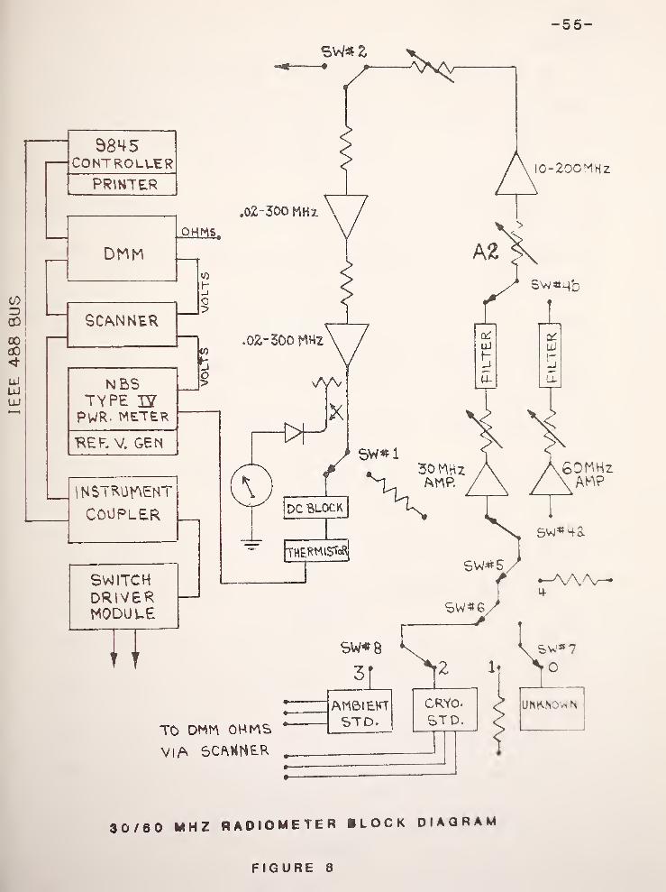
Refer to Figure 2. This is a functional block diagram of
the noise measurement system. To calibrate or find the output
noise temperature of the device under test, the output noise
powers of this device, the ambient standard, and the cryogenic
standard are amplified, filtered, and measured in sequence. The
noise temperatures of the two standards are well known. Using
the noise equations detailed on page 16 of this manual, the
output noise powers and noise temperatures of the two standards
are compared with the output noise power of the device under test
resulting in the determination of the output noise power of this
device. These noise power comparisons are made by using the
30/60 Mhz radiometer system described in t’ e following
paragraphs .
For purposes of explanation, the 30/60 MHz radiometer system
as shown in Figure 3, can be divided into four general parts
which are: (1) the switching and noise source section, (2) the 30
or 60 MHz preamplifier section, (3) the output amplifier and
power measurement section, and (4) the instrument and controller
section.
The switching section provides for selection of the unknown
or standard noise sources for comparison by the system. The
unknown coaxial noise source is usually a noise diode network at
an effective temperature of approximately 11,000 K or a load
which i 8 either heated to a temperature of approximately 376 K or
cooled with liquid nitrogen to a temperature of approximately

-5
uio
SIMPLIFIED
BLOCK
DIAGRAM
OF
NOISE
MEASUREMENT
SYSTEM

IEEE
488
BUS
- 6 -
30 /60 MHZ RADIOMETER BLOCK DIAGRAM
FIGURE 3

K. The normal system range covers this region. The two noise
standards used to calibrate these unknown noise sources over
this range are a coaxial ambient standard and a coaxial cryogenic
standard .
The ambient noise standard is a load placed in an oil bath
which is allowed to come to equilibrium with room temperature.
The controlled room temperature of the standards laboratory, the
mass of the standard housing, and the oil bath insure slow
teraoerature change of the load element and thus a stable noise
power output. Normally, this temperature change is less than 0.05
K over an 8 hour period. The temperature of the standard is
measured often enough to pick up any small temperature changes
wh ich do occur.
The cryogenic standard is similar to the ambient standard
except that the load is housed in a bath of liquid nitrogen. The
temperature of these loads is measured by 3 -wi r e- p 1 a t i n urn
thermometers which are remotely read by the instrument and
controller section. Both standards have tunable output ports
which provide for impedance matching and are currently connected
£o the system with 1 A mm coaxial fittings and air lines.
Precision adaptors are used to connect the standards and unknown
noise sources to the system ports where necessary. Coaxial
connector types currently accepted for the item under tes.
include but are not limited to: precision N, GR900, APC7, and
SMA.
Noise power from the item under test is amplified by either
the 30 MHz preamplifier or the 60 MHz preamplifier. These

- 8 -
frequencies were selected to meet the needs of NBS calibration
service customers. The frequency channel is remotely selected by
the ganged switches at the input and output. The two channels are
similar but the gain of the 30 MHz amplifier is 70 dB while that
of the 60 MHz amplifier is 35 dB. The noise bandwidth of the two
amplifier channels is determined by the amplifier and filter
combination and is 0.77 MHz for the 30 MHz channel and 1.38 MHz
for the 60 MHz channel. The system bandwidth at these frequencies
is not critical as long as the input noise being amplified is
constant over the bandwidth being used. The band widths above
meet this specification. Since they have a noise figure less
than 1.6 decibel, these amplifiers contribute little additional
noise to that being amplified. They are not available
commercially and were designed and built at NBS.
The output from the preamplifier section is amplified by
three additional broadband amplifiers. The first has a bandpass
of 10 to 200 MHz and the second and third have a bandpass of 0.02
to 300 MHz. All three have a gain of 30 decibels. The
attenuators in this section are used to isolate components and to
provide for linear operation. The output of this section is
sampled through the side arm of a directional coupler to give the
operator a visual indication of system power levels.
Power output is measured by using a thermistor mount
connected to the output port through a DC (direct current) block.
This thermistor mount in combination with an NBS Type IV Power
Meter and a precision reference voltage generator is used to
measure noise power.

The instrument and controller section encompasses all of the
peripheral electronic equipment used to make the noise
measurements including the controller, which in this case is the
Hewlett Packard 9845 desktop calculator.
As shown at the left in Figure 3, the peripheral instruments
are all interconnected on an IEEE 488 Bus. The instrument
coupler shown connects the coaxial switch driver module to the
controller. The switch driver assembly is the only instrument not
compatable with the bus and so the instrument coupler, a
sophisticated decoder, is used to interface the switch driver
module to the c on t r o 1 1 e r--mak i ng it bus compatable. This switch
driver module is used to control the various system switches and
programmable and reference attenuator assemblies when they are
used. An LED (light emitting diode) display on the front panel
of the switch driver module gives a visual display of the digital
code from the controller and the front panel meter indicates
system output power levels. The scanner provides connection, at
the proper time, of the ohmmeter section of the DMM (digital
multimeter) to the platinum thermometers in the noise standard
housings. Total resistance, lead resistance, and thermometer
element resistance are determined. Conversion of these
resistances to temperature is done by the software.
A check of system voltages is made by the DMM with proper
connections made by the scanner before each measurement. Voltages
checked include the 15V, 20V, 24V, and 28V switch driver and
amplifier power supplies. In addition, the voltage output of the
power meter is connected to the DMM through the scanner to
collect output voltages which are then converted to power and

- 10 -
noise temperature by the software.
B. ANATOMY OF A MEASUREMENT
A brief description of a measurement sequence is as follows:
1) The impedance of the device to be tested is measured and
input to the computer along with the c onne c t o r / a d a p t o
r
description and associated loss constants. Instructions
for making the impedance measurements are found on page
22; the loss constants are discussed on page 18.
2 The temperatures of the ambient and cryogenic standards
are determined and stored.
3) The powers from the device under test, ambient standard,
and cryogenic standard are measured and the temperature
of the unknown noise source is calculated. This is
normally done 100 times.
4) At the end of the first 50 measurements, the average
noise temperature of the unknown is stored along with
the standard deviation, calculated system temperature,
and average power measured. If the printed results are
obviously erroneous (values far from nominal or with
very large standard deviations), the operator can abort
the measurements at this time, correct the problem, and
start over. Doing this at this point saves time. If the
results printed are acceptable, the cycle is then
repeated starting at 2) and the 2nd 50 measurements are
made. The results are again stored.
5) A grand average of all measurements is obtained and a
summary of results is output via the system printer.
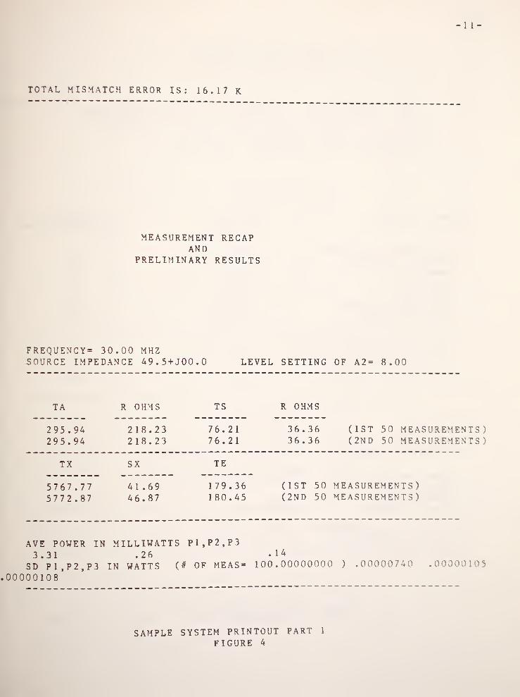
TOTAL MISMATCH ERROR IS: 16.17 K
MEASUREMENT RECAPAND
PRELIMINARY RESULTS
F REQUENC Y= 30.00 MHZSOURCE IMPEDANCE 49.5+JOO.O LEVEL SETTING OF A2 = 8 .00
TA R OHMS TS R OHMS
295.94 218.23 76.21295.94 218.23 76.21
36.3636.36
(1ST 50 MEASUREMENTS)(2ND 50 MEASUREMENTS)
TX SX TE
5767.77 41.69 179.36 (1ST 50 MEASUREMENTS)5772.87 46.87 180.45 (2ND 50 MEASUREMENTS)
AVE POWER IN MILLIWATTS P1,P2,P33.31 .26
SD PI , P 2 , P 3 IN WATTS ( # OF M E A S = 100.00000000 ) .0000074 0 . 0 0 0 0 0 1 0 5
00000108 ’
SAMPLE SYSTEM PRINTOUT PART 1
FIGURE 4

- 12 -
FREQUENCY = 30. MHZ
NOISE TEMPERATURE = 5770. 32K +- 91.20K(BIAS) +-EXCESS NOISE RATIO= 12.76DB + - . 0 6 DB ( B I A S+3 * S EMRADIOMETER SYSTEM TEMPERATURE = 180K ( 2.1DB NF)RADIOMETER GAIN = 76.4DBRADIOMETER NOISE B ANDW I DTH = 1 38.00 MHZ
3.26K (3*SEM:
ERROR SUMMARY
SOURCE OF ERROR SOURCE % ERROR INUNCERTAINTY NOISE TEMPERATURE
CRYOGENIC STANDARD 0 . 28K . 1 2
AMBIENT STANDARD 0. 10K .04POWER RATIO 0.01D3 .49MISMATCH 0 . 5R ; 1 . 0 J OHMS .28NONLINEARITY 6 . 90E-24 .00SWITCH ASSYMMETRY 0 . 002DB .08ADAPTOR : GR900/N 0 . 000 1DB 0 . 00
LINEAR SUM OF BIAS ERRORS 1 .023 * S T AN DARD ERROR OF MEAN ( // M E A S = 100.) .23
LINEAR SUM OF ERRORS 1 .25
CUSTOMER
:
CHECK STANDARDCUSTOMER'S STATION: NBSCUSTOMER'S ADDRESS: BOULDER, COLORADO 80302
SOURCE MANUFACTURER:SOURCE TYPE:
HEWLETT PACKARD C OMPANY
SOURCE MODEL: 3 4 6BSOURCE SERIAL: 6000T
DATE OF CALIBRATION:CALIBRATION TEST //
:
REQ OR REF #:
JULY 10, 1981
SAMPLE SYSTEM PRINTOUT PART 2
FIGURE 5
- 13 -
This summary is shown in Figure 4. The first item at
the top of the page is the total mismatch error in K.
This is followed by the date and time of calibration.
The calibration frequency, impedance of the device under
test, and system attenuator (A2) setting are printed
next (documenting the A2 setting is an aid in
reconstructing the measurement system power levels).
Ambient standard temperature (Ta), cryogenic standard
temperature (Ts), and the associated platinum
thermometer resistances in ohms are then listed followed
by the measured temperature of the calibrated item (Tx),
the standard deviation of the measurement (Sx). and
calculated system temperature (Te). All of these
parameters are listed twice, furnishing a recap for each
set of 50 measurements. Average powers measured are
tabulated with their associated standard deviations.
Pls p2 ,
and P3 are the average powers measured for the
device under test, the ambient standard, and the
cryogenic standard respectively. Standard deviations
for these powers are listed in the same order.
6) Figure 5 shows the final measurement results and error
summary output at the end of the measurements. It
simply details the results and gives a tabulation of
s y s t em errors
.
7) Finally, all information in the measurement
summary, results, and error summary is stored, if
desired, for future reference.

- 14 -
The ensuing discussion of the measurement process gives a
more detailed description of how the above results were obtained.
Since the coaxial noise standards are the basis for determining
the noise temperature of the device under test, the error due to
temperature uncertainty of these two standards must be known.
The size and shape of these standards prevents a direct
attachment to the measurement system, and as a result, the losses
and temperature gradient in the adaptors and precision air lines
used to make connection to the system were calculated and
included in this temperature uncertainty.
The error attributed to these standards is listed in the
error summary output by the system software and is 0.1 K for the
ambient standard and 0.28 K for the cryogenic standard.
The mismatch error is due to the difference in port
impedance between the device being tested and the measurement
system. The error due to mismatch listed by the software is the
root sum of squares of the errors determined for worst possible
cases in phase and magnitude of this port impedance difference.
It takes into account the impedances and the associated
uncertainties of the measurement system ports, the coaxial noise
standard ports, and the output port of the device under test.
This error is dependent on the impedance of the device being
tested and is normally between 0.1% and 0.4% of the noise
temperature measured.
A vector impedance meter is used to determine the impedance
of the source to be calibrated, and then the noise standards are
tuned to match this impedance. The only mismatch error left to
be considered, then, is the difference between the device under

- 15 -
test and the system measurement ports. The system ports have
been measured and found to have the same impedance. The real
part of this impedance was measured to be 49.5 ohms at 30 MHz and
50.5 ohms at 60 MHz. The imaginary part was measured to be 0.0
ohms at 30 MHz and 0.5 ohm at 60 MHz. The estimated uncertainty
is 0.5 ohm for the real part and 1.0 ohm for the imaginary part.
In this discussion, the noise temperature of the device
under test will be designated Tx , and the temperatures of the
ambient and cryogenic standards will be Ta and Ts. Numeric
values for Ta and Ts expressed in K are determined from the
resistance values of the platinum thermometers in the ambient and
cryogenic standards. As mentioned previously, this resistance is
measured and read under computer control and converted to
temperature by the software routines.
During a measurement, the desired port is selected and the
noise power from the device connected to that port is measured
under computer control using the Type IV power meter, reference
voltage generator, and digital multimeter. The reference voltage
output is adjusted to equal the power meter voltage with no rf
power applied to the thermistor mount before the measurements
begin. This zeros the instrument. (Refer to figure 3. Rf power
is removed from the thermistor mount by switching system switch
number 1 to its terminated port.) Power is then determined with
the scanner and system switches providing the proper conditions.
A normal computer controlled sequence is:
1) The power meter voltage (A) is measured with the rf power
of f .

- 16 -
2 The power meter voltage minus the reference voltage (B)
is measured with the power off.
3) The power meter voltage minus the reference voltage (C)
is measured with the rf power on.
4) The power meter voltage (E) is measured with the power
off to check drift.
5) The power meter voltage minus the reference voltage (D)
is again checked with the power off.
6) Power (P) is then obtained by:
P=[ (A+E)-C+(B+D)/2 ] [C-(B+D)/2 ] /RO where RO is the
resistance of the thermistor mount (200 ohms) [1].
The noise power measured from the device under test is
designated PI, that from the ambient standard as P2, and that
from the cryogenic standard as P3. The noise temperature of the
unknown, Tx,
is then determined by first finding the power ratios
Y1 and Y3 and correlating them with the temperatures of the
standards to find Tx:
Y 1 =P 1 / P 2 ( 1 )
Y3=P3/P2 (2)
Tx-Ta+(Ts-Ta)(Yl-l )/ (
Y
3 — 1 ) (3)
Note that because the standards are matched to the unknown,
when Y1 and Y3 are calculated, only the mismatch terms between
the unknown and the system are left to consider. The other terms
cancel since they have been tuned to be equal. Tx is now
determined and now must be corrected for any losses due to the
adaptors or air lines used in connecting the unknown. Losses due
to precision air lines and adaptors have been characterized and

- 17 -
are entered as a constant (Alpha) when the measurement begins.
The corrected temperature of Tx then, is given by:
Corrected Tx= (Tx-Ta ) /A1 pha+Ta( 4 )
where L—Loss in decibels of the adaptors and
air lines used to connect the test device
and Alpha=10“(-L/10)( 5 )
In 3 normal calibration, the determination of Tx is made 100
times and the average of these 100 determinations is reported as
is the standard deviation. Some of the other terms calculated
are as follows [3] :
SYSTEM TEMPERATURE
Te=[Ts-(Y3)(Ta)] / (Y3-1 ) (6)
EXCESS NOISE RATIO dB
ENR=10Log(Tx-290)/ (290) (7)
where 290 is a defined quantity
RADIOMETER SYSTEM TEMPERATURE
RST=10Log(l +T e ) / 2 9 0 (8 )
RADIOMETER SYSTEM GAIN
RSG=10Log[ (7 ,244)(10~13)(P2)/Bw/ ( T a +Ts ) ] (9)
where Bw is the system bandwidth in MHz.
and ( 7 . 2 4 4 ) ( 10 ~ 1 3 ) is a noise constant
The error summary in Figure 5 lists the source uncertainties
on which the error calculation is based. These are the maximum
errors calculated from the source listed. For example, 0.10 K is
the maximum error contributed by the ambient standard.
An in depth discussion of the error calculation is outside the
scope of this manual other than to state that percent error is

- 18 -
tabulated for each source and linearly summed. This sum is the
error recorded on the test report.
3. OPERATING INSTRUCTIONS
A. ADDITIONAL EQUIPMENT REQUIRED
Besides the instruments contained in the measurement system, two
additional pieces of equipment are needed to insure good
measurements. These instruments are:
1. A frequency counter with at least 4 place accuracy: EIP
451D or equivalent.
2. Vector Impedance Meter: Hewlett Packard 4815A or
equivalent .
v
B. GETTING STARTED
When an item is received for calibration, determine first
that the device can be physically attached to the measurement
system. If attachment is physically possible, the adaptor and/or
air line combination needed to make connection should now be
determined and the loss constants with the uncertainty for this
combination is selected from Table 1 and recorded. Table 1 is a
brief s umma ry of common precision hardware used in making
measurements. The frequency, loss constant (alpha), and
uncertainty are listed. The alpha constant for a device is
calculated as follows: First the loss of the device is either
measured or looked up in the manufacturers specifications. Then
alpha is calculated by raising 10 to the minus power of the loss
of the device in question divided by 10. In equation form:
A1 pha= ( 1 0~ ( -dB/ 1 0 ) ) . Device input power multiplied by alpha is

- 19 -
equal to device output power. If more than one item is used, the
correct loss constant (alpha term) and its uncertainty can !> a
computed by multiplying loss constants and adding uncertainties.
C. PREPARING THE SYSTEM FOR MEASUREMENT
1. POWER-OFF INSPECTION AND SETUP
First check all cables and connections. The IEEE 488 bus
cables should provide interconnection between the 9845
calculator, the scanner, the digital multimeter, and the
instrument coupler. The switch driver module input jack ( J 1 1 0 )
should be connected to the instrument coupler output jack ( J 3 )
.
The leads from the ambient and cryogenic standards should be
securely plugged into the receptacles at the left front of the
scanner. Check to make sure that the Type IV power meter and
reference voltage generator are properly interconnected and that
the output cable is plugged into the scanner. System wiring and
interconnection diagrams are found in Section 5 of this manual.
Remove the standards and any other devices from the system
measurement ports and check the system and standard connectors
for damage. It is suggested that the connectors should all be
cleaned with isopropyl alcohol.
F i g ur 6 6 shows the cryogenic and ambient standards as the
cryogenic standard is being filled with nitrogen. Fill the
small liquid nitrogen container shown in the figure with liquid
nitrogen and locate the white filler cap near the tuning knob:-, on
the top of the cryogenic standard. Remove this cap and the two

- 20 -
AMBIENT AND CRYOGENIC NOISE STANDARDS
FIGURE 6

- 21 -
FREQUENCYMHZ
CONNECTOR/ ADAPTORDESCRIPTION
LOSS CONSTANTALPHA
ALPHAUNCERTAINTY
30 GR elbow, adaptor,15cm air line
.99891 .00047
30 GR elbow, adaptor,10cm air line
.99903 .00042
30 GR 15cm air line .99952 . 00021
30 GR 10cm air line .99964 .00016
30 GR elbow .99949 .00023
30 Ad a p t o r-N t o
GR, APC 7 ,SMA
.99985 .00010
60 GR elbow, adaptor,15cm air line
.99843 . 00067
60 GR e 1 bow,adaptor
,
10cm air line.99986 .00060
60 GR 15cm air line .99932 .00030
60 GR 10cm air line .99949 .00023
60 GR elbow .99928 . 00032
60 Adaptor-N to
GR, APC 7 ,SMA
.99985 . 00010
LOSS CONSTANTS AND UNCERTAINTIESTABLE 1

- 22 -
white vent plugs from the standard. Using a funnel, SLOWLY pour
a small amount of liquid nitrogen into the standard. „ After
allowing several minutes for the inside of the standard to cool,
add more nitrogen until the float on the top of the standard
reaches the third red mark. Remove the funnel and replace the
two vent caps and the filler cap.
The impedance of the item to be measured should now be
determined by using the vector impedance meter. This instrument
should be turned on at least one hour prior to making
measurements. To save warmup time this instrument can be turned
on the night before. Connect the RF OUTPUT jack on the front
panel to a suitable frequency counter and set the desired
calibration frequency by using the front panel RANGE SWITCH and
TUNING KNOB. When the desired frequency is obtained, the
instrument can be zeroed by using the PROBE CHECK on the front
panel. Remove the probe from its adaptor by pulling it straight
out and insert it into the PROBE CHECK receptacle. Use the
MAGNITUDE ZERO and PHASE ZERO controls to get meter indications
of 100 ohms and 0 degrees. Now the item can be checked by
attaching the probe assembly to its output connector. If a noise
diode assembly is measured, be sure to apply the voltage
specified by the manufacturer (usually 28V) before making the
impedance measurement. Record the impedance measured for the
item. At this time, the a d a p t o r / c o n n e c t o r loss constant, the
uncertainty of this loss constant, and the impedance of the
device to be calibrated are tabulated for input to the computer
during the measurement.
After the cryogenic standard reaches operating temperature,
- 23 -
tune the standards to the impedance value obtained for the item
to be calibrated. Simply attach the probe and adaptor from the
vector impedance meter to the standard ports and carefully adjust
the standard tuning knobs until the same impedance values are
obtained for both the standards and the unknown. Connect the
ambient standard to the leftmost calibration port (port 3), the
cryogenic standard to the adjacent port (port 2), and the device
to be calibrated to the rightmost port (port 0). The port
adjacent to port 0 (port 1) is not used at this time. Leave this
port terminated at all times. Figure 1 shows the measurement
system with correct devices connected to all ports. If the
device under test is a noise diode network, make sure that the
correct voltage is applied to it.
2. POWER-ON CHECKS AND SYSTEM WARMUP
Before any power supplies are turned on, make certain that
the 30/60 preamplifier voltage switch is in the off (center)
position. This switch is located on the right side of the metal
table as you face the system and opposite the the two
preamplifiers. Moving the switch to the up position turns on the
28 volts to the 30 MHz preamplifier and moving it to the down
position applies 28 volts to the 60 MHz preamplifier.
CAUTION
DUE TO THE HIGH GAIN OF THE PREAMPLIFIERS USED WITH THIS
SYSTEM MAKE SURE THE 30/60 AMPLIFIER VOLTAGE SWITCH IS IN THE OFF
(CENTER) POSITION BEFORE OPENING ANY MEASUREMENT PORT. DAMAGE
WHICH IS EXPENSIVE AND TIME CONSUMING TO REPAIR WILL OCCUR II THE
AMPLIFIER INPUTS ARE SUDDENLY EXPOSED TO AN OPEN CIRCUIT

- 24 -
CONDITION. ONE OR MORE STAGES WILL BE DESTROYED AND THE
AMPLIFIER WILL HAVE TO BE RETUNED AND THE NOISE FIGURE RESTORED.
After making sure the above switch is in the off position,
power-up can be accomplished in the following order:
1. Turn on the controller
2. Turn on the digital multimeter and scanner.
3. Turn on the power meter and reference voltage
generator.
4. Turn on the instrument coupler and press its reset
button.
5 Turn on the switch driver module and press its reset
but ton.
6. Now turn on the 28V, 25V, 24V, and 15V supplies.
7. After all measurement ports have devices attached to them
it is safe to place the 30/60 preamplifier voltage switch
in the 30 MHz (up) position or the 60 MHz (down) position
as required.
It is good practice to let the system warm up or cool down,
as the case may be, at least 2 hours before continuing.
3. LOADING AND EXECUTING THE MEASUREMENT PROGRAM
There are two measurement programs which are used; one for
30 MHz calibrations called ,, 30M20" and one for 60 MHz called
"60M20". The programs are stored on disc and cassette tape. If
it is desired to load a program from cassette, insert the program
cassette in the right hand tape drive (T15) and type MASS STORAGE
IS ":T15"; press Execute. Type LOAD "30M20" for example;press

- 25 -
Execute. The program will now be loaded from cassette. The
procedure for loading the program from disc is the same - except
that the MASS STORAGE IS statement is changed to MASS STORAGE IS
":F8". The disc is placed in the left hand drive and the "LOAD
30M20" instruction when executed, loads the program from the
disc.After the program is loaded, press RUN. The system should
make a series of 5 measurements as evidenced by numbers moving on
the CRT display and clicking of the measurement switches. At the
end of the five measurements, an average value of power at the
measurement port #0 will be displayed. Adjust attenuator A2,
(The precision manual step attenuator with the knobs above the
plexiglass system cover) until the value of this measured power
is 3 milliwatts. This is done by pressing RUN and adjusting the
attenuator and then pressing RUN again to check the result. When
the power level measured and displayed is 3 milliwatts
consis tantly ,press the CONT (continue) button on the 9845 . The
system constants should now be displayed on the screen. A
listing of these constants is available in the software portion
of this manual but the important thing right now, is that they
are present and displayed. If this is true, press CONT again.
At this point, the program section which requests operator
input is reached. The software is designed to be as friendly as
possible and whenever information is requested, a prompt
describing the information required is displayed and the
information requested by the prompt which is currently In m e m o r
>
is displayed. To leave the information as is, press only the
space bar followed by CONT. If a change is desired, type the

- 26 -
change in the same format as the sample displayed; then press
Cont to go on. Information is requested by the measurement
program in this order:
1. Enter the loss constant, alpha. This is the total alpha
for all connectors, adaptors, and air lines used to
connect the device under test.
2. Enter the uncertainty for the alpha in 1 above.
3. Enter the real and imaginary impedance of the device
being tested in ohms. This is a literal representation
of impedance in this form: 50.0 +J00.0. This input will
be used in a printout.
4 Enter the real and imaginary impedance of the noise
source being calibrated. This is a request for the real
and imaginary parts of impedance in numeric form:
50.0,00.0. This input will be used in calculations.
5. Enter the item description.
a) Enter the customer's name.
b) Enter the customer's street address.
c) Enter city, state, zip.
d) Enter the manufacturer of the device under test.
e) Enter type number of device under test.
f) Enter model number of device under test.
g) Enter serial number of device under test.
h) Enter date of calibration.
i) Enter NBS Test Number
j) Enter reference Number
At this time the program returns to a) and the entire

- 27 -
description can be checked by pressing the SPACE BAR and
CONT unless a change is desired. To enter corrections,
simply type that line over and press CONT.
6. Enter the setting of attenuator A2. Type in the setting
in dB of the manual attenuator dials.
This concludes operator entry of data. The system will now
run a check of the resistance and temperature of the standards
and then check the system voltages. The date, time and standard
temperatures measured in degrees Kelvin will be printed. A
summary of system voltages and standard resistances measured will
be displayed. If everything is satisfactory, press CONT.
The system will now do a complete measurement and error
analysis under computer control and print the information shown
in Figures 4 and 5. While the measurements are in progress, a
print of all powers measured, device temperature calculated, and
the standard deviation of the measurement is printed continously.
Portions of the measurements such as power meter voltage readings
are displayed on the screen in real time enabling a visual check
of individual parts of the measurement. This is very helpful in
finding trouble if erroneous measurements are made.
At the end of the 100 measurements and the printout of
Figures 4 and 5, the program requests a data cassette to be
inserted in the left hand deck and by following the instructions
printed out, a complete recording of all results and d o \ i «. c
description is made. A complete catalog of the tape contents . s
maintained for easy access to data in the future if desired.
After the data are recorded, the software requests the
additional 3 dB in attenuator A2 and pressoperator to insert an
- 28 -
run. This is a routine system linearity check and is a complete
repeat of the measurement just described at a different power
level. The results of the second set of measurements should
closely agree with the first set. Agreement within 0.2% should
be expected. The outside limit is one half of the total error
printed out for the first measurement. If the outside limit is
exceeded, the system should be suspected of nonlinearity and all
equipment should be checked to determine the cause.
In addition, check standards (devices which can be measured
to evaluate system performance) are maintained which give a good
indication of measurement integrity. These standards include a
noise diode "tree" which incorporates three noise sources
arranged with attenuators to give three different noise power
outputs. The effective noise temperatures available from this
standard are approximately 11000 K, 6000 K, and 3000 K.
Measurement of this standard checks system performance over a
broad temperature range. A physical temperature check standard
with output noise temperatures of approximately 377 K and 77 K
provides a check of system performance at these temperatures. It
is intended to routinely cablibrate these standards and establish
a control chart which will closely monitor system and standard
performance. Not enough measurements have been made at the
present time to establish a statistically signifigent chart.
Measurements at this time show a total spread below 0.3%. The
outside limit for measurement acceptance is estimated to be 0.5%
of the measured value at this time. Measurements outside this
specification indicate trouble with either the measurement system

- 29 -
or the standard itself.
D. SYSTEM TURN-OFF
This procedure is essentially the reverse of turn-on
and should be done in the order below.
1. Turn off the preamplifier voltage with the switch
located on the side of the table.
2. Carefully turn the voltage down on the noise diode
power supply (if used) and turn the supply off.
Remove the calibrated item and replace it with a
termination to protect the measurement port.
3. Turn off the system power supplies.
4. Turn off the instrument coupler, switch driver
module, digital multimeter, scanner, power meter,
and reference generator.
5. Turn off the 9845 and vector impedance meter.
If the measurements are to continue soon, uncouple the
cryogenic standard from port 2, and refill it with liquid
nitrogen. This will sustain its internal temperature allowing
measurements to resume without waiting for the standard to
stabilize .

- 30 -
4. SOFTWARE
A. GENERAL DESCRIPTION AND SUBPROGRAMS
The measurement programs ,, 30M20" and "60M20" are written in
a structured fashion. By this it is meant that each program
consists of an executive section which contains the measurement
sequence and provides for the orderly gathering of information by
accessing the subprograms [4]. Variables exist in the executive
program and the subprograms, but are not passed between the
program segments unless they are made "global" by being listed in
the common declaration or in the subprogram calling statement.
All subprograms used in these programs are of the multi-line
function type. These subprograms are nested in the program after
the executive portion, and are identified by the prefix "DEF
FN...(Q)" where Q is the variabl being passed between program
segments. Variables passed between segments in these programs
are made "global" by being listed in the common declaration at
the beginning of the program and at the beginning of each
subprogram as well. These common declarations must match. The
value returned from the subprograms by the calling statement is a
dummy variable which is not used. In these programs values are
passed between segments by use of the common declaration. The
advantage of this programming technique is the ease with which
subprograms can be called from any point in the program without
regard to the variable transfer in the calling statement (since
variable transfer is through common). The drawback is that each
subprogram has to have a common declaration to match the one in
the main program.

- 31 -
The instrument subprograms are flexible and easily changed
to permit a change of instruments. Because subprogram Input and
output variables are transferred as described above, the only
changes needed to permit a change of instruments are the
instrument instruction codes output on the bus to each instrument
from the controller. This is necessary because few different
instruments respond to exactly the same coded set of
instructions. A standard instruction format for control of
instrument functions does not exist at this time.
Figure 7 shows the program structure and the relationship
between the executive program and the primary subprograms which
are called from it. The subprograms are essentially independent
of one another and require only a proper calling sequence to
provide the desired output. This output will be returned to the
calling program segment.
As an explanation and clarification of Figure 7, a discussion of
major program segments follows:
EXECUTIVE SEGMENT provides program constants and input of
needed parameters; control is then passed to EXECUTIVE SUBPROGRAM
FNQ.EXECUTIVE SUBPROGRAM FNQ is called from the EXECUTIVE
SEGMENT; it directs program sequence and provides for orderly
execution of program instructions. FNQ provides calls to FNE to
initialize software and hardware, to FNJ to get item description,
measurement parameters and port assignments, and to FNK to start
measurements, compute results, print results, and store results.
Return is to the EXECUTIVE SEGMENT.

EXECUTIVE. SEGMENT
-32-
lil
£E
3O
- 33 -
SUBPROGRAM FNE is called from FNQ; FNE(O) performs necessary
hardware reset while FNE
(
1 ) initializes the software. Return is
to FNQ.
SUBPROGRAM FNJ is called from FNQ; FNJ(l) provides for input
or confirmation of item under test description. FNJ(2) provides
number of measurements, frequency, and system attenuator
setting. FNJ(3) provides the measurement system port assignments.
Return is t FNQ SUBPROGRAM FNK is called from FNQ; FNK(O) starts
measurement sequence by calling subroutine FNL and also sets up
and begins filling the L, Z, and M matrices. These matrices will
be covered in detail later in this section. FNK(l) performs
necessary calculations for error analysis and completes filling of
the L , M, and Z matrices. FNK(2) provides a call to FNVswr to get
mismatch error and outputs measurement results to the printer.
FNK( 3 ) provides for storage of measurement results, temperature,
pressure, and item description on tape or disc. Return is to
FNQ .
SUBPROGRAM FNData is called from the EXECUTIVE SEGMENT; it
provides for reading of stored data and printing of results, item
description, and other information in the proper format. Return
is to EXECUTIVE SEGMENT.
SUBPROGRAM FNP is called from the EXECUTIVE SEGMENT before
measurements are started to enable setting of system power.
Return at this time is to EXECUTIVE SEGMENT. This subprogram is
also called from FNV during the measurement sequence to provide
an output power determination from the device under test and the
standards. Return is to FNV.
from real time clock is requested by EXECUTIVE andTIME

- 34 -
SUBROUTINE FNM to provide date and time information. Return is
to the calling segment.
SUBPROGRAM FNL is called from FNK; it provides calls to FNT
for standard resistances and system voltage check, to FNA for
conversion of standard resistances to temperature in K, and to
FNM to initiate measurements. Return is to FNK.
SUBPROGRAM FNM is called from FNL; it provides calls to FNV
and FNG to get measurements and a real time plot of results. It
also prints results and computes standard deviation. Return is
to FNL.
SUBPROGRAM FNV is called from FNM; it calls FNP for power
measurements and computes the value of Tx (noise temperature of
item being calibrated). It also computes the standard deviation
of measured quantities and averages. Return is to FNM.
SUBPROGRAM FNA is called from FNL; it provides calculated
temperatures of the standards. It requires constants relating to
the resistance of the platinum thermometers in the standards.
Return is to FNL.
SUBPROGRAM FNVswr is called from FNK; it provides calculated
mismatch error for the item under test in K. It requires
impedance parameters for the item under test and the system as
well as Tx , Ta , and Ts values for the measurement. Return is to
FNK.
SUBPROGRAM FNX has no direct call; it provides port and
frequency code to the switch driver module when required. Return
is to the calling segment.
B. MATRICES

- 35 -
Four matrices are used to store the program constants and
measurement results. They are:
1) The N matrix-- a 26 X 1 1 matrix which contains all system
constants used in computations. These include the platinum
thermometer corrections, system errors and their sources, alphas
and their uncertainties, and reserved space for additional
constants to be added, if necessary, in the future. Table 2 is
a listing of the contents of the N matrix with descriptions of
the various parameters. This matrix is automatically read from
the storage medium into computer memory when the program is run.
2) The L matrix— a 1 by 12 matrix which is used for
intermediate storage of measurement results and standard values.
3) The M matrix— a 1 by 33 matrix contains the L matrix
information and, in addition, contains the measurement results,
statistics, error analysis results, and standard values. Table 3
shows the contents of the M matrix.
4)
The Z matrix— a 1 by 60 matrix which is the output matrix
for the measurement program. Table 4 is a listing of the Z
matrix contents.
The above information concerning the various program storage
registers is presented as an aid in program analysis if this is
desired
.
Appendix I of thi manual contains a complete program listing,
printout of variables used, and their location in the program.

- 36 -
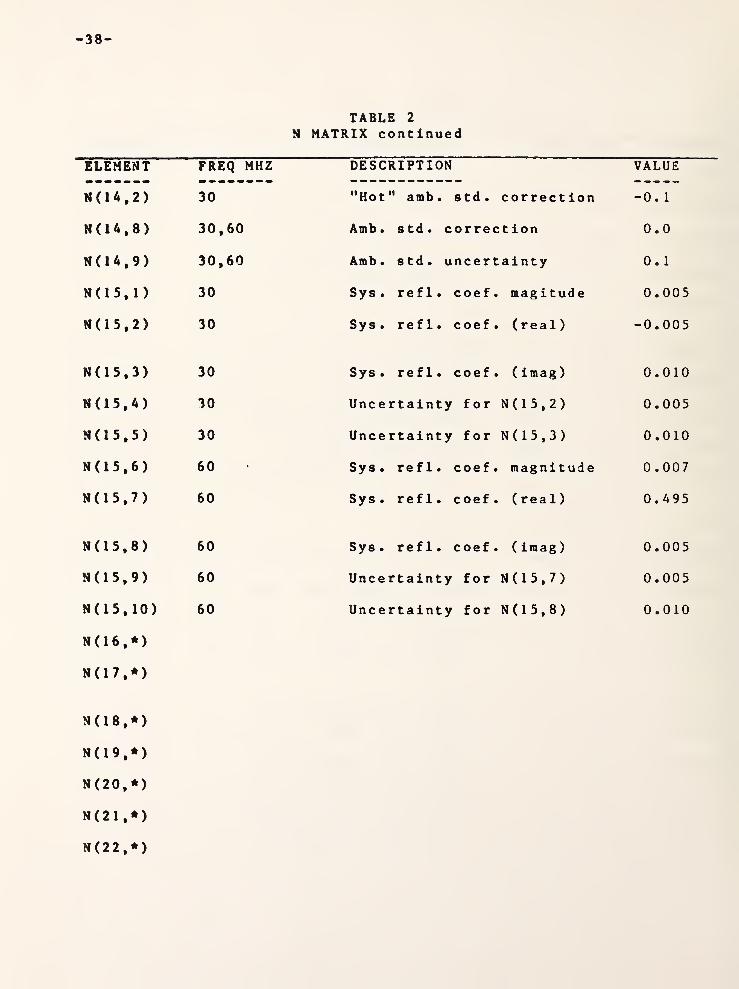
TABLE 2
N MATRIX
ELEMENT FREQ MHZ DESCRIPTION VALUE
*N ( 1 ,*) System if
6
constants
N ( 2 , 1 ) "Hot" ambient std. 200. 158
N ( 2 , 2 ) "Hot" ambient std. 0.00391775
N ( 2 , 3 ) "Hot" ambient std. 1 .50289
N ( 2 , 4 )" Hot" ambient std. 0.12293
N ( 3 , 1 ) Cryo. std. in amb. range 199.965
N(3,2) Cryo. std. in amb. range 0 .003922
N(3,3) Cryo. std. in amb. range 1.51
N ( 3 , 4 ) Cryo. std. in cryo range 0.11
N(4 ,*)
N ( 5 ,* )
N ( 6 , 1 ) Cryo. std. in cryo. range -0.00065732
N(6,2) Cryo. std. in cryo. range 32.7792
N ( 6 , 3 ) Cryo. std. in cryo. range 1 .20769
N(7,l) WCD std. 0.0
N(7,2) WCD std. -6.53922
N ( 7 , 3 ) WCD std. 0.0210573
N(7,4) WCD std. 65.1189
N(8,*)
N(9,*)

- 37 -
TABLE 2
N MATRIX continued
ELEMENT FREQ MHZ DESCRIPTION VALUE
N ( 1 0 , 1 ) 30 "a" non-linearity 2.15 E - 2 2
N ( 1
0
, 2 ) 30 System noise bandwidth 0.773
N ( 1
0
, 3 ) 60 "a" non-linearity 3.32 E - 2 3
N ( 1 0 , 4 ) 60 System noise bandwidth 1 .38
NCI 1 ,*)
N ( 1 2 , 1 ) 30 Cryo. std. uncertainty K 0.22
N ( 1 2 , 2 ) 30 "Hot" amb . std uncertainty K 0.22
N ( 1 2, 3 ) Power ratio source (dB) 0.01
N ( 1 2,4 ) 30 "a" non-linearity" 2.15 E - 2 2
N ( 1 2, 7 ) 30,60 "switch assymmetry source 0.002
N ( 1 2 , 8 ) 30,60 N term 0 . 00047
N ( 1 2 , 9 )Power to gain constant 7.244 E+13
N ( 1 3 , 1 ) 30 Real Z fixed amb. ohms 50.5
N ( 1 3
,
2 ) 30 Imag. Z fixed amb. ohms 1.0
N ( 1 3 , 3 ) 30 Mismatch error, fixed amb. 0.368651
N ( 1 3 , 7 ) 60 Cryo. std. uncertainty 0.28
N ( 1 3 , 8 ) 60 "Hot" amb. std. uncertainty 0.25
N ( 1 3 , 9 ) 60 Cryo. std. correction 0.38
N(13, 10) 60 "Hot" amb. std. correction -0.15
N ( 1 4 , 1 ) 30 Cryo. std. correction 0.26
38 -
TABLE 2
N MATRIX continued
ELEMENT FREQ MHZ DESCRIPTION VALUE
N(14,2) 30 "Hot " arab. std. correction -0.1
N ( 1 4 , 8 ) 30,60 Atnb
.
std. correction 0.0
N(14,9) 30,60 Arab
.
std. uncertainty 0.1
N ( 1 5 , 1 ) 30 Sys . refl. coef. magitude 0.005
N ( 1 5 , 2 ) 30 Sys . refl. coef. (real) -0.005
N(15,3) 30 Sys . refl. coef. (imag) 0.010
N ( 1 5 , 4 ) 30 Uncertainty for N(15,2) 0.005
N ( 1 5 , 5 ) 30 Uncertainty for N(15,3) 0.010
N ( 1 5 , 6 ) 60 Sys . refl. coef. magnitude 0.007
N ( 1 5 , 7 ) 60 Sys . refl. coef . ( rea 1
)
0.495
N ( 1 5 , 8 ) 60 Sys . refl. coef . ( imag
)
0.005
N ( 1 5 , 9 ) 60 Uncertainty for N(15,7) 0.005
N(15 t 10) 60 Uncertainty for N(15,8) 0.010
N ( 1 6 ,* )
N ( 1 7 ,* )
N ( 1 8 ,* )
N ( 1 9 ,* )
N (20 , *
)
N ( 2 1 ,* )
N ( 2 2 ,* )

- 39 -
TABLE 2
N MATRIX continued
ELEMENT FREQ MHZ DESCRIPTION VALUE
N ( 2 3 ,* )
N ( 2 4 , 1 ) 30 Total alpha of GR adapt., 0.99891
N ( 2 4 , 2 ) 30ell, and 15cm air lineUncertainty for N(24,l) 0.00047
N ( 2 4 , 3 ) 60 Total alpha of GR adapt., 0.99943
N ( 2 4 , 4 ) 60ell, and 15cm air lineUncertainty for N(24,3) 0.00067
N ( 2 5 , 1 ) 30 Alpha for 15cm air line 0.99952
N ( 2 5 , 2 ) 30 Uncertainty for N ( 2 5 , 1 ) 0 . 00021
N ( 2 5 , 3 ) 60 Alpha for 15cra air line 0.99932
N (2 5 , 4 ) 60 Uncertainty for N(25,2) 0.00030
N ( 2 5 , 6 ) 30 Total alpha of GR adapt.. 0.99903
N ( 2 5 , 7 ) 30
ell, and 10cm air line
Uncertainty for N(25,6) 0.00042
N ( 2 5 , 8 ) 60 Total alpha of GR adapt., 0.99986
N ( 2 5 , 9 ) 60
ell, and 10cm air lineUncertainty for N(25,8) 0.00060
N ( 2 6 , 1 ) 30,60 Alpha for adaptor--N to 0.99985GR, APC 7 ,
or SMA

- 40 -
TABLE 2
N MATRIX continued
ELEMENT FREQ MHZ DESCRIPTION VALUE
N ( 2 6 , 2 ) 30,60 Uncertainty for N(26, 1) 0.00010
N ( 2 6 , 3 ) 30 Alpha for GR ell 0.99949
N ( 2 6 , 4 ) 30 Uncertainty for N(26, 3) 0.00023
N ( 2 6 , 6 ) 30 Alpha for GR 10cm air line 0.99964
N ( 2 6 , 7 ) 30 Uncertainty for N(26, 6) 0.00016
N ( 2 6 , 8 ) 60 Alpha for GR ell 0.99928
N ( 2 6 , 9 ) 60 Uncertainty for N(26, 8) 0.00032
N(26, 10) 60 Alpha for GR 10cm air line 0.99949
N (26 , 1 1 ) 60 Uncertainty for N(26, 10) 0.00022
* Note: an * in the matrix element description denotes all
columns of the indicated row of the matrix.

- 41 -
TABLE 3
M MATRIX
ELEMENT DESCRIPTION PROG LOCATION
M( 1 , 1 ) Frequency F 3050
M(1 ,2) // of Freq and Levels 3060
M(1 ,3) L ( 1 , 1) =T 2 P 0 = 1 3070
M(1 ,4) L ( 1 , 2 ) =T 3 P 0= 1 3080
M(1 ,5) L ( 1 , 7 )=T2 P 0 = 2 3090
M(1 ,6) L ( 1 , 8 ) = T 3 P0 = 2 3100
M(1 ,7) L ( 1 , 3 ) =T
1
P0 = 1 3110
M(1 ,8) L ( 1 ,4)=S1 P 0 = 1 3 120
M(1 ,9) L ( 1 , 5 ) = T 4 P0 = 1 3130
M(1 , 10) L ( 1 , 9 ) = T 1 P 0 = 2 3140
M ( 1 , 1 1 ) L ( 1 , 10)=S1 P0 = 2 3150
M(1 , 12) L ( 1 , 1 1) =T 4 P 0 = 2 3160
M ( 1 ,1 3 )
T 1 Average = Tx 3 170
M(1 , 14) Standard error of mean 3450
M(1 , 15) T4 or Te average 3480
M ( 1 , 16) T2 average = Ta 3 5 00
M ( 1 ,1 7 )
T3 average = Ts 3520
M( 1 , 18) Linear sum of bias errors 3790
M( 1 ,1 9 )
3 times std . error of mean 3800
M(1 ,20) Linear sum of errors 38 10

- 42 -
ELEMENT
M ( 1 , 2 1 )
M(1 ,22)
M(1 ,23)
M(1 ,24)
M(1 ,25)
M(1 ,26)
M(1 ,27)
M(1 ,28)
M(1 ,29)
M ( 1 , 30 )
TABLE 3
M MATRIX continued
DESCRIPTION
Excess noise ratio of Tx (dB)
Bias plus 3 times std. error
Ambient standard error
Cryogenic standard error
Power ratio error
Non-linearity error
PROG LOCATION
3820
3850
3550
3560
3680
3690
Standard error of
Switch assymmetry
L ( 1 ,6) = P2 P 0 = 1
mean 3460
error 3 7 70
3170
M ( 1 , 3 1 ) L ( 1 , 12) = P2 P0 = 2 3180
M(l,32) Average power from ambient 3860
M ( 1 ,33) Radiometer gain in dB 3620

- 43 -
TABLE 4
Z MATRIX
ELEMENT DESCRIPTION PROG LOCATION
(1,1) T 2 P0 = 1 6490
(1,2) T 3 P0=1 6500
( 1 ,3 ) T 1 P 0=
1
6510
( 1 , 4 ) SI P0 = 1 6520
(1,5) T 4 P 0 = 1 6530
Z(1 ,6) P 2 P 0 = 1 6540
Z ( 1 , 7 ) T 2 P 0 = 2 6550
Z( 1 , 8 ) T 3 P 0 = 2 6560
Z ( 1 ,9) T 1 P 0 = 2 6570
Z( 1 , 10) P 2 P 0 = 2 6580
Z(1 , 11 ) T 4 P 0 = 2 6590
Z ( 1 , 1 2 ) P 2 P 0 = 2 6600
Z(1 ,13) 3 times std. error (Tx) 4650
Z ( 1 ,14) Excess noise ratio in dB (Tx) 4700
Z(1 , 15) Bias plus 3 times std. error 47 10
Z(1, 16) Te ,
radiometer sys. temp K 4740
Z ( 1 , 1 7 )System noise figure 4750
Z ( 1 , 18) System gain in dB 4800
Z(1,19) N ( 1 2 , 1 )
— s. error cryo. std. 4900
Z(1 ,20) % error-cryo. std. 4910

- 44 -
TABLE 4
Z MATRIX continued
ELEMENT DESCRIPTION PROG LOCATION
Z ( 1 ,21 ) N(14,9), ambient std. s. error 4940
Z ( 1 ,22) % error- ambient std. 4950
Z ( 1 ,23) N(12,3), power ratio s. error 4980
Z ( 1 ,24) % error- power ratio 5020
Z ( 1 ,25)
Z(1 ,26) Total mismatch error K 5010
Z ( 1 ,2 7 ) N(12,4) "a" non-linearity 5040
Z ( 1 ,28) % error for non-linearity 5050
Z ( 1 ,29) % error for switch assymmetry 5090
Z( 1 , 30) Linear sum of bias errors 5170
Z ( 1 ,31 ) Total # of measurements, N 52 30
Z ( 1 ,32) % Error- 3 times SEM 5240
Z ( 1 ,33) Linear sum of errors 5280
Z ( 1 , 34 ) Frequency F 4510
Z ( 1 ,35) Calibrated Tx (average) 4630
Z ( 1 ,36) Bias error 4640
Z(l,37)
Z ( 1 ,38)
Z ( 1 , 39 )
Z( 1 ,40)

- 45 -
TABLE 4
Z MATRIX continued
ELEMENT DESCRIPTION PROG LOCATION
Z ( 1 ,41 ) Sum of sqrs Tl, 2nd 50, B6 92 90
Z ( 1 ,42) Sum of Tl, 2nd 50, B8 93 10
Z ( 1 ,43) Sum of sqrs Tl, 1st 50, B5 93 50
Z ( 1 ,44) Sum of Tl, 1st 50, B7 9360
Z ( 1 ,45) Sum of PI (divide by N for a v e ) 9520,9600
Z(1 ,46) Sum of P2 (divide by N for a ve ) 9530,9610
Z ( 1 ,4 7 ) Sum of P3 (divide by N for a ve ) 9540,9620
Z ( 1 ,48) Sum of sqrs PI 9550,9630
Z ( 1 ,49) Sum of sqrs P2 9560,9640
Z(1 ,50) Sum of sqrs P3 9570,9650
Z ( 1 ,51 ) A2 atten. setting 2690
Z(1 ,52) Tl 3240
Z(1 ,53) T 2 3250
Z(1 ,54) T 3 3260
Z ( 1 ,55) N term .00047 3860,5400
Z ( 1 ,56)
Z(1 ,57) N ( 1 2 , 8 ) switch assymmetry 3850
Z ( 1 , 58 )
Z ( 1 , 59 )R2 amb. std. thermometer res. 11290
Z ( 1 ,60) R3 cryo. std. thermometer res. 1 1300

- 46 -
C. EQUATIONS
To provide a reference for the theoretical work underlying
the algorhythms used in the software, a summary of equations used
in the software (in addition to those in part 2) is presented at
this point. This summary is not intended to be self-explanatory.
In the following discussion, T1 is the temperature measured for
the device under test, T2 is the temperature of the ambient
standard, T3 is the temperature of the cryogenic standard, and T4
is the calculated system temperature, Te . The resulting errors
in T1 are reported in K.
CALCULATION OF AMBIENT STANDARD TEMPERATURE
Definition of Terms:
C
1
=2
0
0 . 1 5 8 Note: C1-C4 are constants supplied for the
C2=0 . 0039 1 77 5 ambient standard platinum thermometer.
C 3= 1 . 50289
C 4 =0 . 1 2293
T2=Temperature of the ambient standard in K.
R=Measured resistance of the ambient standard platinum
thermometer
.
Computation: (iterate to invert the Ca 1 1 ond e r-Van Dusen equation.)
H 3= ( R/ C 1 - 1 )/C2 ( 1 )
If H3 is greater than 0 set H9*0; otherwise set H9*C4.
G9=H3/100 ( 2 )
G 8 = G 9- 1 (3)
If H3 is greater than 0 set H3«H3+C3*G9*G8; otherwise set
H3=H3+C3*G8*G9+H9*G8*G9*G9 (A)
T 2 =*H 3 + 2 7 3 . 15 K (5)

CALCULATION OF CRYOGENIC STANDARD TEMPERATURE
Definition of Terms:
Cl— 0. 00065732
C 2 = 3 2 . 7792
C3-1 . 20769
T 3=Calculated cryogenic standard temperature in K.
R=Measured resistance of the cryogenic standard platinum
the rmomet e r
.
Computation: (from a polynomial fit)
H 3 = C 1 *R “ 2 (6)
T 3 = C 2+C 3*R+H 3 K (7)
AMBIENT STANDARD UNCERTAINTY (U) is 0.1 degree K.
at 30 and 60 MHZ
.
R8= (T1-T2) ' ( T 3-T 2 ) (8 )
where T1,T2, and T3 are the temperatures in K of
the unknown device, ambient standard, and cryogenic standard
respectively.
Let ES2=the error due to the ambient standard in measuring
the unknown.
ES2=ABS(1-R8)*U (9)
CRYOGENIC STANDARD UNCERTAINTY (U) is 0.22 degree Kelvin at 30
MHz and is 0.28 degree K at 60 MHz.
Let ES 3=Er ror due to the cryogenic standard uncertainty in
measuring the unknown.
E S 3 =AB S ( R 8 *U )< 10 )
UNCERTAINTY IN MEASURING POWER RATIOS is 0.01 dB.
Power factor (U) *0.0023

- 48 -
Let EPR=Error due to uncertainty in measuring power ratio.
A= 1 +T 4 / T 1 (11)
B= 1 -T 2 / T 1 (12)
C = (T 3+T 4)/ (T3-T2) (13)
EPR=ABS [U*(A-B*C) ] (14)
SYSTEM NON-LINEARITY CONSTANT (a) is 3.32 *10~-23 at 60 MHZ and
2.15 * 1 0 ~-2 2 at 30 MHz
.
Bandwidth (B)= 1 . 38MHz at 60 MHz and 0.773MHz at 30 MHz.
Radiometer Gain in dB=G
Let ENL=Error due to system non-linearity.
ENL=ABS [(a)*10"(G/10)(B)(10“6)(Tl-T3)*(Tl-T2)] (15)
UNCERTAINTY OF THE SWITCH SETTINGS IS 0.002 dB and the constant
for switch assymmetry is 0.00047.
Let ES4=The error due to switch assymmetry.
A = AB S [ (T1)(T3) + (T1)(T2) + (T2)(T3)/(T3-T2)] (16)
ESA =A*0. 00047 ( 1 7 )
SOURCE UNCERTAINTY (U) OF THE ADAPTOR / CONNE CTOR LOSS is
0.0005 (O.OOOldB).
Let EAL=Error due to a d a p t o r / co n ne c t o r loss.
Cl=Alpha for the connector adaptor combination
C2=Uncert ainty for alpha.
C3=C1*2 (18)
A-l-l/Cl (19)
B=Bias Error(Linear Sum) (20)
C = A* B (21)
D = A* . 1 (22)
E = ABS [ (T1-T2)/C3*(C2) ] (23)
E AL = B +D+E (24)

To Calculate the OUTPUT NOISE TEMPERATURE of a Device
when an adaptor has been used in its calibration
use the following:
Tx = T 1 * A+T a * ( 1 - A ) (25)
where Tx is the output noise temperature of the
device. T1 is the noise temperature with the adaptor
attached, Ta is the ambient temperature in K
(the nominal value of Ta is 300 K),
and A is the alpha for the attenuation present.
A is calculated by: A=10~(-Loss dB/10) (26)
STANDARD DEVIATION is calculated by:
S.D.=Square root of ( ( V -T*T /N ) / (N - 1 ) ) (27)
where T is the sum of the individual measurements;
V is the sum of the squares of the individual measurements,
and N is the total number of measurements.
STANDARD ERROR OF THE MEAN is given by:
SEM=S
.
D . / Sq ua re root of N (28)

- 50 -
5. MAINTENANCE
A. EQUIPMENT DESCRIPTION
Since the measurement system is largely made up of
commercially available equipment, operating, periodic
maintenance, and troubleshooting Instructions can be found in the
appropriate manual supplied with the instrument. A list of the
equipment presently being used, the manufacturer, and the model
number follows
:
IMPORTANT NOTICE
The specific components selected for use with the system
were chosen on the basis of suitability, availability, and cost.
They do not necessarily represent the only possible choice or
even the best choice. The National Bureau of Standards states
only that they were used in the system described here.
Substitution of nominally equivalent components meeting the same
specifications should cause no difficulty; however NBS has not
tested all such possible choices.
INSTRUMENT NAME MANUFACTURER MODEL
1 . Cont roller Hewlett Pa cka rd Co . 9845B
2. Digital Multimeter John F. Fluke Co • 8502A
3. Scanner Hewlett Packard Co
.
3 4 9 5 A
4. Instrument Coupler ICS Electronics Corp
.
4883
5 . Ampli f ier Aertech A 1 5 1 7
6 . Ampli f ier Avantek AV-4
- 51 -
INSTRUMENT NAME MANUFACTURER MODEL
7. Power Supplies Power Mate Corp BP34D
8 . Preamplif ier NBS 30MHz
9 . Preamplif ier NBS 6 0MHz
10. Noise Standard NBS Ambi ent
11. Noise Standard NBS Cryogenic
12. Switch Driver Module NBS 30-60
1 3 . Power Meter NBS Type IV
Technical details, schematic diagrams, and parts lists for
the switch driver module and the 30 and 60 MHz preamplifiers are
included in this manual. Also included are wiring diagrams and
system cable information. Technical information pertaining to
the ambient and cryogenic noise standards can be obtained by
contacting L.D. Driver, Division 723, National Bureau of
Standards, Boulder, Colorado 80302.
B. SYSTEM CHECKS
A number of checks are performed automatically in the
process of making a measurement with the system and its software.
These include: 1) A check of system power measurements which is
made by running the system power set portion of the program at
the beginning of a measurement sequence. If the power meter,
reference generator, and digital multimeter are not performing
adequately, this fact will be made apparent by the values
displayed during this program segment. Erratic and obviously
wrong power values and large variations between consecutive
measurements are the usual indication of malfunction of these

- 52 -
ins t ruraent s . System frequency and measurement port switches are
also exercised during this test and defective switching can cause
a substantial spread in measurement results, no change in power
when a measurement port is changed, or a null to be read at one
or more ports.
2) System voltage check-s are made automatically before the
measurement sequence begins. The values of these voltages are
displayed along with the platinum thermometer resistances and
noise standard temperatures. The operator must approve the
displayed values before measurements continue. These checks
reaffirm that the voltmeter and ohmmeter portions of the digital
multimeter are working properly, that intercabling between
instruments is intact, and that the system power supplies are
adjusted and functioning properly.
3) Large scatter in successive readings of power and temperature
taken during a calibration are an indication of erratic switch
operation or poor peripheral instrument performance. Experience
will dictate what this scatter should be for a given item. Three
times the standard error is normally below 1 percent of the noise
power measured.
In addition, system operation is verified in two other ways
during a measurement sequence.
1) Measurement of the device under test at two different power
levels is required and will pinpoint system non-linearity. 2)
Applicable reference standards with effective noise temperatures
of 11000, 6000, 3000, 377, and 77 degrees K are checked
immediately before or after a device is calibrated to test system
accuracy. These measurements provide an excellent check of

- 53 -
overall system performance. Results obtained by measurement of
the reference standards are the single most important indicator
of system precision and accuracy. These results will show
whether or not a major failure has occurred in such a subtle
manner that the failure was not detected by other checks.
If the system fails to perform properly during any of the
tests, try to pinpoint the location of the trouble by logically
analyzing in which test the trouble occurred, and working
backwards to isolate the instrument or component responsible for
the failure. For example, if a switch is intermi t tant,
the tests
outlined will give an indication of the measurement port involved
(possibly a large scatter in power measured at one port). Switch
operation then can be isolated to the faulty switch and/or driver
card by parts substitution and in-circuit testing.
In the event that a major repair is made on the system
preamplifiers or input port switches, a complete analysis of the
impedance and noise figure of the radiometer "front-end" should
be made and impedance parameters contained in the N-raatrix
changed if necessary. System linearity and bandwidth should a 1 s o
be re — evaluated and the constants relating to these parameters
changed in the N-matrix if necessary.
Diagnostic tests of commercial units, to which faults have
been isolated, can be performed by following the instructions
provided in the applicable operation and service manual.
No specialized diagnostic software has been written to aid
in troubleshooting the equipment because the above described
tests will isolate most faults to at least the instrument level.

54
C. COMPONENT DESCRIPTION AND TECHNICAL INFORMATION
For commercial equipment used in the system,- this
information is available in manuals supplied by the manufacturer.
1. SWITCH DRIVER MODULE
This instrument is comprised of power supplies, remote
switches, a decoder card, LED display, switch driver output
cards, and an output display card with its associated analog
meter. The output display card is the only card requiring
adjustments and these are covered with the description for this
card .
a) Power Supplies and Switches
The switch driver module contains one 5V power supply
which supplies operating voltage for the integrated circuits
on the decoder, switch driver, and output display cards.
15V and 25V drive voltages for the switches controlled by the
switch driver cards are also supplied to this unit from
external power supplies after passing through two remotely
controlled switches. This permits the drive voltage for the
system switches to be turned on and off by the controller.
Also present in the unit are the positive and negative 15V
supplies for the operational amplifiers on the output
display card.
b) Card 110, Decoder Card.
This card uses a type 7442 decoder chip which is a BCD to
decimal decoder (1 of 10). Four of these elements are used;
one spare which is presently not used is supplied. Figure
10 shows the truth table for this type of decoder chip. In
IEEE
488
BUS
- 55 -
30/60 MHZ RADIOMETER ILOCK DIAGRAM
FIGURE 8

- 56 -
CRS|7 *
27 •—
^
5 ,.CT L7400
u io -AAAA ,-t-Sv
FLS.
33 0 CR9
35 1 OR 10
38 2 CRU40 3 CRi2
Ml 0-1 CftlS
43 2-3 CR\4
% 0-3 CR\5
48 4 CP.1&
M9 30 CRP
51 60 CR\8
54 CR 23
56 CR 24
7 CR 1?
8 CR 20
9CR 21
6 CR22
110 DECODER CARD SCHEMATIC DIAGRAM
FIGURE 9

- 57 -
SN7442
BCD INPUT DECIMAL OUTPUT
D C B A 0 8 9
0
0
0
0
0
0
0
0
1
1
1
1
1
1
1
0
0
0
0
1
1
1
1
0
0
0
0
1
1
1
0
0
1
1
0
0
1
1
0
0
0
1
0
1
0
1
0
1
0
1
0 1
1 0
1 1
1 1
1 1
1 1
1 1
1 1
1 1
1 1
1 1
1 1
0 1
1 0
1 1
1
1 1
1 1
1 1
1 1
0 1
1 1
1 1
1 1
1 1
1 1
1 1
1 1
1 1
1 1
1 1
1 1
1 1
0 1
1 0
1 1
111111 1
DECODER CHIP TRUTH TABLE
FIGURE 10

-58-
110 DECODER CARD PARTS PLACEMENT
FIGURE 11

- 59 -
Figure 10, the BCD (binary coded decimal) inputs labled D,
C, B, A correspond to device pin numbers 15, 14, 13, and 12
respectively. The decimal outputs listed correspond, in
ascending order, to device pin numbers 1 through 11.
Inputs from the controller are sent to the decoder card
via the instrument coupler. These inputs are decoded and
sent to the proper switch driver card to achieve the desired
switch action. Referring to Figures 8 and 9, outputs from
pins 33, 35, 33, and 40 on this card control the switching
of ports 0, 1, 2, and 3. Outputs from pins 41 and 43 select
either the port 0-1 position or the port 2-3 position of
switch ^6. Outputs from pins 46 and 48 position switch #5
to connect ports 0-3 or port 4 to the remainder of the
measurement system. Outputs from pins 49 and 51 select
either the 30 Mhz or the 60 MHz position of switches 4a and
4b. As can be seen in Figure 9, input pin 24 on the decoder
card is the "strobe" input for all of the decoder chips.
This signal is used to enable the decoder output. Removing
this signal provides for removing switch current without
disturbing switch position. This signal is utilized in this
manner to prevent heating of the switches. Outputs from
pins 7 and 8 on this card are used to control the remote
switches for the 15V and 25V power supplies for the switch
drivers. The output from pin 9 on this card is used as 3
control bit for the thermistor mount switch and provides for
removing current from this switch after it is properly

- 60 -
posit ioned . The output from pin 6 on this card is the return
flag signal to the controller from this card.
The LED display on the front panel of the switch driver
module originates on the decoder card. The upper 8 bits of
the display represent the digital input bits to the decoder
since a LED is connected to pins 10, 21, 12, 13, 14, 15,
16, and 17. The lower portion of the LED display is formed
by connecting a LED to each of the following output pins:
33, 34, 38, 40, 41, 43, 46, 48, 49, 51, 54, 56, 7, 8, and 9.
By observing the lower portion of the display, the output of
the decoder card can be determined at any time,
c) Switch Driver Cards
The switch driver module uses two different switch
driver designs. One is intended to use the decoder outputs
to control switching. This configuration is found on cards
111, 112, and 113. The other model uses a data bit and a
control bit from the controller with no decoder in between.
This configuration is found on card 114. Use of this card
represents a hardware update to utilize a design
incorporated in new equipment now being built for other
systems. Cards 111, 112, and 113 control the system
measurement port and frequency switches. Referring to
Figure 12, the cards are configured for the decoder input
model by installing jumper wires between points B and C, and
points D and E with no connection between points D and C and
points A and B. There are 4 complete switch driver circuits
on a card; Figure 12 shows only one of these circuits for
illustration purposes with inputs and outputs for all

183
62
°^hZ
+
- 61 -
cruo»o_K)
<T>
Nl
>in
OOO
TcC
OuJu~>
n
cn
o£
rO
QC
LO
Oocn
o
zlUcn
jJ
oa:
ot~occxJ>
2<X0<O
oK<2UJ
XoCO
ax<o
XUJ
>Xa
xa
rs a £CO
cO is><£ <z
uJ UJ
cP
K~
<s 1
Y~“cr s13 aro
vro
r3 a
<m'V
oi
33 o
FIGURE
12

DS 0025
7400
7M04
1
-7HO©i
!
i
nisiU3
1
1
UH
DS002B~-^
D3 DH
SWITCH DRIVER CARD PARTS PLACEMENT
FIGURE 13

four circuits indicated by multiple pin numbers. Inputs are
in pairs and produce outputs in pairs (inputs of the proper
polarity at pins 46 and 48 produce outputs of opposite
polarity at pins 9 and 7). Connected to opposite sides of a
switch, these outputs cause it to toggle with a change in
polarity. Inputs which cause the paired outputs to have the
same polarity produce a positive voltage which is applied to
both sides of a switch. There is no current flow, and as a
result, the switch does not toggle. The system port
switches if 1 and if 8 are controlled by the outputs of driver
card 111. The action of switches if 5 and if 6 is controlled
by driver card 112. The frequency selection switches if 4a
and if 4b are controlled by the output from driver card 113.
Card 114 is similar to the other switch driver cards
but, as previously mentioned, is designed to operate without th
decoder. To configure this card, remove the jumpers
described previously and install jumpers between points A
and B and points D and C.
Binary bit 7 or decimal 128 from the decoder card is
used as the enabling input for the drivers on this card. It
is applied to pin 19 on card 114. The source for this
control bit is the controller.
d) 117 Output Display Card Operation and Adjustment
Figures 14 and 15 are the schematic diagrams for this
card. The output display printed circuit card monitors the
output of the diode detector. The input on pin 13 is
- 64 -
amplified by IC-501 and input to the overload level
comparator, IC-506, through the overload-adjust
potentiometer "H" (R5). If the rf power exceeds 5
milliwatts the overload comparator triggers and latches.
This energizes the sonalert alarm and overvoltage LED via
Pin 52. The comparator cannot be reset by pressing the
reset button until the power level has been reduced to a
safe level .
The incoming signal level is also processed through a
series of amplifiers to the front panel RF level meter. The
output of the log-amplifier, IC501, passes through a sample
and hold circuit, IC-502. The output of the sample and hold
circuit drives the log-amplifier, IC-504, to convert the
meter reading to a dB scale. IC-503 forms a constant current
source to set the zero reference of the log amplifier. The
output of IC-504 is connected to the input of the meter
driver amplifier, IC-505. The gain of this amplifier is
switched for gains of 10, 1, and .1 to obtain meter scales
of 1.0 decibel, 0.1 decibel, and 0.01 decibel. Potentiometer
"D" ( R 1 4 ) adjusts the times 1 scale zero reference.
Adjustment of the Output Display Card
This is the only card in the switch driver module which
requires adjustment. Adjustment is necessary only when the
circuit has been repaired. The adjustments establish the
logarithmic amplifier gain for the decibel scale on the
front panel signal level meter and set the overload alarm
threshold. Complete alignment requires two, 1 mi 1 1 iampere

- 65 -
Q
:
pUi2
OQ

-66 -
Q—
5 v
o—
I ACOoN
xj- MY - 13
J-II7- I!
o~ x ,oi
+
FP
51
OUTPUT LEVE.V-Ma
Overload
-o 1 o^ RESET
45v«^.
+5v ^
OOVtRLO.^D^
-OR.F. OR (6 )
SI .
52"
d nr
/o b
Z 6
30
£3
43
33:
I I
|4
1
|
27
32
34
H9
H7
54
117 OUTPUT DISPLAY CARD FRONT PANEL CONNECTIONS
FIGURE 15

-67
117 OUTPUT DISPLAY CARD PARTS PLACEMENT
FIGURE 16

- 68 -
constant current sources. Refer to Figure 14 when
adjustment of the 1700 card is performed. Adjustments
should be made in the following order:
1. Mount the 1700 printed circuit card on a PC extension card
and remove the signal input cable from the diode detector
to the front panel.
2. Connect an external voltmeter between TP 1 and ground.
Adjust "A" (R7), DC offset of first amplifier, for zero
on the voltmeter.
3. Connect the external voltmeter to TP V and adjust offset
control, "C" (R9) for a zero reading on the voltmeter.
4. Remove the jumper from TP V to TP W. Connect a temporary
jumper from TP X to TP Y. Adjust "E" (R19), DC offset of
the first log-amplifier, for a zero voltmeter reading.
5. Remove the temporary jumper from TP X to TP Y. Remove
the jumper from TP Z to TP Zl. Connect one +1
milliampere constant current source into TP Zl from
ground. Connect the other +1 milliampere constant
current source into TP W from ground. Set both current
sources to 1 milliampere. (Place two suitable current
meters in series with the sources and adjust the output
of the current sources to 1 milliampere on these
meters). Connect the external voltmeter between TP 2
and ground. Adjust "F" (R20), the DC offset of the
second stage of the log amplifier, for zero volts on the
vol tmet e r
.
6. Remove both constant current sources. Replace the jumper

- 69 -
frora TP V to TP W. Replace the jumper between TP Z and
TP Z 1 .
7. Connect a suitable cable between the DET IN jack on the
front panel and the system diode detector output
connector at on end of coaxial switch // 1 .
(a) Place a diode noise standard on port 0 and apply
voltage (normally 28 volts) to it.
(b) After making sure all ports are properly
terminated, turn the measurement system on.
(c) Place the preamplifier voltage switch to the 30
MHz or up position.
(d) Turn on all system power supplies.
(e) Load the measurement program (3 OH 20).
(f) Type the following on the 9845 keyboard:
OUTPUT 702 ; "0","0"
,"7 ", "0"
PRESS EXECUTE
(g)
Remove the termination from the auxiliary port on
system switch If 1. Place a suitable thermistor
mount on this port and connect it to an external
powe r meter.
(e) Set attenuator A2 for 1 milliwatt of system output
power at this port.
8. Connect an external voltmeter to TP 1. Adjust B (Ro't, the
first amplifier gain, for 1 volt on the voltmeter.
9. Adjust system attenuator A2 to set the external power meter
reading to 2 milliwatts. Switch the meter range

- 70 -
selector on the front panel to the XI position. Adjust
"D" (R14), log reference zero offset, for a zero reading
on the front panel signal level meter.
10. Increase the setting of system attenuator A2 by 5 dB. Adjust
"G" (R21), log-amplifier gain, for a front panel meter
reading of -5 divisions. Decrease the attenuator A2
setting 10 dB and note the front panel meter reading.
Touch up "G" if necessary to obtain approximately a +5
reading on the meter scale. Recheck the -5 reading.
1 1 . Set the input attenuator for a power level of 1 milliwatt on
the power meter. Readjust "D" for a +3 reading on the
front panel meter.
12. Adjust the front panel attenuators for a 5 milliwatts
(+7dBM) power indication on the power meter. Adjust
"H" (R5), overload threshold adjust, clockwise until
the alarm sounds. Now turn R5 1/2 turn counter-
clockwise. Reduce the input power and push the
reset button on the front panel. Slowly increase the power
to test the alarm threshold. The alarm should be
activated at the +5 milliwatt power level.
13. Adjust attenuator A2 until the external power meter reads 2
milliwatts. Adjust "D" (R14), log reference zero
offset, for a zero reading on the front panel signal
level meter.
This completes the alignment of the Output Display
Card. These adjustments do not affect system operation or
accuracy. They do however, provide for the accurate display of
system power levels

2. 30 MHZ AND 60 MHZ PREAMPLIFIERS
Referring t o Figure 17, note that essentially the same
schematic diagram is used for both the 30 MHz and the 60 MHz
preamplifiers
.
The main difference is the value of the RF
chokes, LI and L2. The values of these components in the 30 MHz
amplifier are double the value of those used in the 60 MHz
amplifier.
These amplifiers were very carefully built with extreme care
being taken with parts selection and placement. Ground strapping
is extremely important as is proper shielding. Some stock
components as well as some component locations produced an
inferior amplifier. For this reason, amplifier performance was
checked with impedance and noise figure meters as construction
progressed .
Input impedance, output impedance, and noise figure are
adjustable. However, because the adjustments are interdependent,
a compromise is necessary to obtain optimum tuning for both noise
figure and impedance. The lowest noise figure achieved with
acceptable input impedance was between 1.5 and 1.6 decibels.
This noise figure was obtained while maintaining the real and
imaginary parts of the input impedance as specified previously.
The impedances were measured using a vector impedance meter, in 1
the noise figure was measured using a commercial noise figure
meter with a calibrated noise diode reference.
Since failure of one of these amplifiers will undoubtedly
cause a long "system down time" while repairs and adjustments are
made, spare amplifiers are mounted beside the two being used. It

- 72 -
30MHZ
AND
60MHZ
PREAMPLIFIER
SCHEMATIC
DIAGRAM

- 73 -
failure occurs, simply remove the defective amplifier and replace
it with the proper spare.
3. INTERCONNECTION AND WIRING DIAGRAMS
The system interconnection cables include the IEEE 488 bus
cables which connect the controller to the scanner, digital
multimeter, and instrument coupler. In addition to the
instrument bus interconnection cables, the equipment is coupled
together by the following:
TABLE 5
SYSTEM CABLES— INSTRUMENTS TO SCANNER
Cable # Figure it Source Destination
1
.
Cable 1 1 8 DC Power Supplies Scanner
2 . Cable 14 18 Scanner DMM Rear PanelInput Connector
3 . Cable 2 1 8 Type IV Power Meter Scanner
4 . Cable 2a 18 Scanner Rear PanelInput Connec tor
5 . Cable 3 19 Ambient Standard External TerminalBoard on Scanner
7 . Cable 4 1 9 Cryogenic Standard External Te rrain il
Board on Scanner
8 . Cable 5 1 9 External TerminalBoard on Scanner
DMM Front PanelInput Terminals
The cables listed 1 n Table 5 are those directly concerned
with the transfer of measurement information from the various
ins t rument s t o the digital multimeter which acts as a central
processing point since it measures the cable outputs and sends
the measured results back to the controller on the IEEE 4S8 bus.

Commands from the controller are sent to the switch control
module via the instrument coupler. The switch control module
then controls the system switches by accessing them through the
cables connected to its output jacks. Figures 20 through 28
detail the pin connections of the switch driver module input and
output jacks.
An overview of all connections made to the switch driver
module from the controller and within the switch driver module to
the various switch driver cards is shown in Figure 20.
Figure 21 is a diagram of J104 which is the input cable from
the instrument coupler to the switch driver module.
Figure 22 is a diagram of J102 which is the output jack from
the switch driver module to the system switches.
Figure 23 is a wiring list for J-102 and its associated
cable.
Figure 24 is a diagram showing the inputs and outputs to J-
110, the decoder edge connector.
Figures 25 through 28 are diagrams of the switch driver card
edge connectors J-lll, J-112, J113, and J 1 1 4
.
4. PARTS LISTS
Information relating to the parts lists for the digital
voltmeter, scanner, instrument coupler, thermistor mount, power
meter, and power supplies can be obtained from the instrument
manual supplied by the manufacturer. The parts lists for NBS
manufactured equipment will be found in TABLE 7. Manufacturers
Codes used in these parts lists are tabulated in TABLE 6.

- 75 -
TO Dm
TO DMH
SCANNER DECADE (LOW THERMAL) CHANNELS 10-19
H L
10'
1 10
+28 v 1 1-28v 1
1
+ 15 v 12 - 15 v 12
+ 20v 13 -20v 13
14 14
TYPE IV+DVMOUT 15 TTPE IV-DVn 15
rvs out r ’ 16 P VS —OUT 16L
' 17 17
18 16
19 19
TOSHIELD
GRP
10
11
12
13
m15
16
17
ie
_I_9_
SCANNER CONNECTIONS CABLE 1 (10-13)
SCANNER CONNECTIONS CABLE 2 (15-17)
POWER METER WIRING DIAGRAM AND SCANNER CONNECTIONS
FIGURE 18
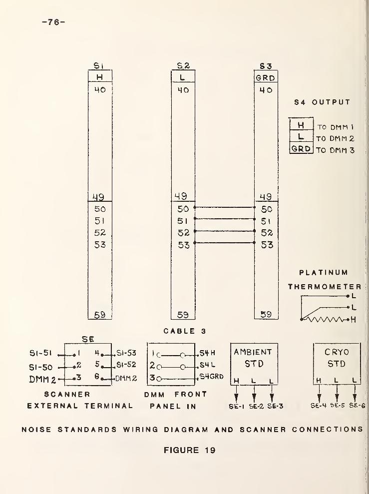
-76 -
Sl-51 ,
Si -50
DMM2
St
H
HO
S2
50
5 !
5255
59
S3L GRDHO HO
H9
i
1
i
i
l
M950 J
’ 505 1
1
' 5 \
52 ' 52
53 ( 53
59 59
S 4 OUTPUT
H
GRD
TO DMN I
TO DMM 2
to Dnn 3
* L
CABLE 3SE
. 1 H « „Sl-53 I r O - „S*f H AMBIENT CRYO,$|-52
V, 1 1 vJ
p S4 L STD STD
—»z +Dmz 3o ,S4GRDX r r H L L
SCANNEREXTERNAL TERMINAL
DMM FRONTPANEL IN
T T TSE-I SE-2 SE-3
PLATINUM
THERMOMETER• L
T \ 1SE-4 ^E-5 SE-6
NOISE STANDARDS WIRING DIAGRAM AND SCANNER CONNECTIONS
FIGURE 19

jno
- 77 -
oCM
LU
cc“5
BY8TEM
CABLE
INTERCONNECTION
DIAGRAM

-78 ”
J-104
GHD V !
00 (5 B SPARE
00 14 c,
SPARE
DO 13 D J 116,-43
DO 12 £ 0 \\G-
DO II!
F : J IIS' ^3
Do |0i H JU5> 17
BOO!
J JIM' M3
DO 8 ! K JIlH- 17
DO Ti
L!
0 II0-Z7
DO 6 ni J no-26
DOS:
n:
J 110-25
DO 4.p J 1
10-24
DO 5 R ! 4 ! S0"23
DO# s1
J i io-22
DO 1 T!
0 IIO-ZI
DOO U ! J 110-20
"PCNTL|
wI
vilio-5
I/O1x
!
U ISO- 28
?FLG F A Aj
j no- 6
GND Da ! oCJDio
PIN CONNECTIONS FOR J 1 0 4 , SWITCH DRIVER MODULE INPUT
FIGURE 21

•J 10£
-79
Acf Sw5 + d 112-35
0111-21 SW7+ B!
i e J 115-35J IIM-&I C
! f
D hE j SW5- JII2-39
Oil 1-25 SW7- F K J 1 15~ 39
J 114-25 Hi tn
d IT
Kt> sw + dU3-2l
0 1 11-35 SW8+ L r 0MG-2I
0 114-35 M s
N tP T3 Sw - J 113-25
dl 1 1-3R SW8- R 0 1 16- 25JH4-34
| s Ul)
i T Xj u
:M SPARE J 113-35
J Il2‘2l SW6+|V 1 !
Z
d 116- 35J 115-21
1 W AA
t
X BBi Y C C
»
SPASE J 113-39
J 112-25 SW6- z DD|
0H6-39J N5-25 a ZZ !
t
b F F
c HHJ
PIN CONNECTIONS FOR J102, SWITCH DRIVER MODULE OUTPUT
FIGURE 22
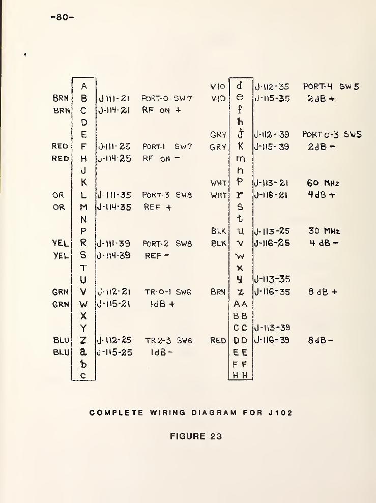
-80-
i
A Vio a
BRN B 0111-21 PORT-O SW7 VIO eBRN C 0-114- 21 HF oh + f
D hE GRY J
RED F d-IU-25 Port- l Sw7 GRY K
RED H 0 U4-25 RF on - m0 hK WHT 9
OR L 0-111*35 PORT-3 SW8 WHT rOR M 0-im-35 ref + s
N t
P BIK UV£l R O-ui-39 Port-2 sws blk VYEL S 0*114-39 REF — vv
T Xu y
6RN V 0-1 12- 21 TR- o-i SWG BRN 2CRN w 0-H5-2I IdB + AA
X BBY CC
BLU z 0-B2-25 TR 2-3 SW6 RED DOBLU a 0-H5-25 IdB- EE
t> F F
c H H
0112*35
0*115-35
0-112-39
J-M5-39
0-113- 21
O-lie-21
J- 113-25
J-II6-25
0-113-35
O-UG-35
J-U3-39
jHIG-33
COMPLETE WIRING DIAGRAM FOR J102
PORT* H SW 5
2d8 +
PORT 0-3 SW5
2dB -
60 MHz
HdB +
30 MHz.
H 06-
8 dB +
8dB-
FIGURE 23

-81 -
tJ 110
1 31
% 32+5 v / 3 33 J in -nTB4 ^
4- 34
J |0<f - W 5 35 0 111-19
0 ton - AA 6 3G+ 25v SWITCH 7 37•+ l5v SWITCH 8 38 J 111-41
15,16- M|*l9 3 3910 Ho J III- 43
" H 1 J 1 12-17
\ 2 H 2
S 3 M3 J |12- 19
1 4 H H
1 5 H 5
i G HG J 1 12-m
1 7 4 7
1 6 48 8 112-43
1 3 H9 0 113-17
0 104- U 20 50
J | 0M- - Ti
51 J 113-19
J 104- S 22 52
J 104- R 23 53
J 104- P 24 54 J 113-41
J lo4 - N 25 55
J 104- M 26 56 0113-43
\) 104- L 27 57
i) 104— X 2 8 58
23 59 *1 — 5 V GNO
, 5-P— 60 J TB-
J110, DECODER CARD INPUT AND OUTPUT CONNECTOR
FIGURE 24

82-
J III
l 31
2 32
3 33
|
4 34
3 356 367 378 383 3910 4 0
1
1
H 1
\Z M213 431 4 M H
15 4516 46
J no -33 17 4718 46
J 110-35 19 4 9
20 50vl 102-6 21 51
22 5223 5324 54
J 102-F 25 S 5
26 5627 5728 58
+ 15V TB 29 59_£C> 6o
-ISV TB
0 102-L
Uioa-R
0 ) 10-38
vj 110-40
>gno
Jill, SWITCH DRIVER CARD INPUT AND OUTPUT CONNECTOR
FIGURE 25

-83 -
d 112.
1 31
Z 32
3 33
+ 34
5 356 367 378 389 3910 40
li 41
12 42
13 4314 44
15 45
16 46
d 110-41 17 47
18 48
dHO-43 19 49
20 50
d I0Z-V 21 51
22 5223 5324 54
d 102*2 25 55
28 56
27 1 57
28 59
+ 15 T& 29 59
_22_ 60
-I5T6
d 102 -d
d 102-
J
d U0-M6
dUO-46
GND-TB
GND-TB
J112, SWITCH DRIVER CARD INPUT AND OUTPUT CONNECTOR
FIGURE 26

-84-
vJ 113
I 31 -!5vTB2 323 334 3M
5 35 o \oz-x
6 367 378 389 39 d 102-CC
10 Hd
l» HI dllO-54
\Z 42
I13 43 dHO- 56
:H 44
|15 45
i IB 46JIIO-M9 17 47
18I 4&
JllO-51 19|
49
20|
5021 51
i 22 52
123 5324 54
J 102-ju 25 ' 5526 5627 57
: 28 58-+I5VT& 29 59 \ -TB
3£l L_6oJ GND
J 1 1 3 , SWITCH DRIVER CARD INPUT AND OUTPUT CONNECTOR
FIGURE 27

- 85 -
l
Z;
5 !
4|
5 j
,s
!
I 7
!8 !
9 !
(
10
11
12
13
14
15
16
vJ 104-K 17
18
J UO-9 |9
20•J 102-C 21
22232H
d 102-H 252627
28
1 15 v 2930
d 114
31
323334
353637
38
3840
41
MX
4344
45
4647
48435051
52535455565758
5960 }
-15v TB
d 102-M
JI02-S
duo-9
U 104-J
-TBCND
J114, SWITCH DRIVER CARD INPUT AND OUTPUT CONNECTOR
FIGURE 28

-86-
d 117
ANALOG GND 1 31M II 2 32 FP-47
3 334 34 FP-485 35e 36 - I5v
7 378 38 -H5V9 39 FP-4410 HO
SHIELD XTALDET. II H 1 FP-4512 42
XTAL DET. 13 H3 FP- 4314 H H
15 4516 4617 H 7 FP- 5! LED ft
18 4519 49 FP“ 50 RESET20 50z\ 51
22 52 J-II4-I9
TP-H2 23 532H 54 LED-GRN FP-5225 55
TP- 31 26 56TP- *46 27 57 4* 5 V
TP- *40 28 58 + 5v29 59 GND
TP-41 30 60 tl
J117, OUTPUT DISPLAY CARD INPUT AND OUTPUT CONNECTOR
FIGURE 29

- 87 -
TABLE 6
MANUFACTURER'S CODE TABLE
3M
3M Company, Electronics Products Division
3M Center
St. Paul, Minnesota 55101
ABAllen-Bradley Company
1201 S. Second Street
Milwaukee, Wisconsin 53204
ALCO
Alcoswitch Division of Alco Electronic Products,
P.0. Box 1348
Lawrence, Massachusetts. 01842
AM PH
Amphenol Connector Division
Bunker-Ramo Corporation
Broadview, Illinois 60153
BRNS
Bourns, Incorporated, Trimpot Division
1200 Columbia Avenue
Riverside, California 92507
BUD
Bud Radio Incorporated
4605 East 355th Street
Willoughby, Ohio 44094
Inc.

- 88 -
CORG
DATL
DIAL
DUMC
GARY
ITSL
TABLE 6
MANUFACTURER'S CODE TABLE continued
Corning Glass Works
Electronic Products Division
Corning, New York 14830
Datel Systems, Incorporated
1020 Turnpike Street
Canton, Massachusetts 02021
Dialignt Corporation
Division of North American Phillips Corporation
Brooklyn , New York 11237
Duncan Electric Company, Inc.
2865 Fairview Road
Lafayette, Indiana 47902
Garry Manufacturing, Inc.
1010 Jersey Avenue
New Brunswick, New Jersey 08902
Intersil, Incorporated
10900 North Tantau Avenue
Cupertino, California 95014
- 89 -
MODT
MONO
MOT
NATL
NBS
SAMT
TABLE 6
MANUFACTURER'S CODE TABLE continued
Modutec, Incorporated
18 Marshall Street
Norwalk, Connecticut 06854
Precision Monolithics, Inc.
1500 Space Drive
Santa Clara, California 95050
Motorala Semiconductor Products, Incorporated
2002 West 10th Place
Tempe ,Arizona 85281
National Semiconductor Corp.
2900 Semiconductor Drive
Santa Clara, California 95051
National Bureau of Standards
325 Broadway
Boulder, Colorado 80302
Samtec,Incorporated
2652 Charlestown Road
New Albany, Indiana 47150

- 90 -
TABLE C
MANUFACTURER'S CODE TABLE continued
SCBE
S c a n b e Cinosa Industries
3445 Fletcher Avenue
El Monte, California 91731
SE AC
Seacor, Incorporated
598 Broadway
Norwood, New Jersey 07648
SPRG
Sprague Electric Company
418 Marshall Street
North Adams, Massachusetts 012147
THER
Thermal loy Inc
.
2021 West Valley View
Dallas, Texas 75234

- 91 -
TABLE 7
PARTS LIST FOR SWITCH DRIVER MODULE COMPONENTS
DECODER CARD (110)
Catagory 1 Resistors
R1 lea Resistor, Carbon, 0 . 2 5W 5% AB FSN 5905-681-6462
Catagory 4
CR1-CR24, 24 ea
—--D i odes
LE D Indicator DIAL 550-0506
Catapnry 5— integrated Circuits
Ui, lea I . C . Hex Inverter T
I
SN7404N
U2, lea I . C . Hex Inverter TI SN7404N
U 3 lea I . c. Hex Inverter T
I
SN7404N
U 4 lea I . c . Hex Inverter TI SN7404N
U 5 lea I . c . Decoder TI SN7442N
U 6 lea I . c. Decoder TI SN7442N
U 7 lea I . c. Decoder TI SN7442N
U 8 lea I . c . Decoder TI SN7442N
U 9 lea I . c . Decoder TI SN7442N
U10 lea I . c . Quad Nand Gate TI SN7400N
Catagory 6' Connectors-
1 Oea DIP Socket 14 Pin THER 8204-NF-4 14-1

- 92 -
TABLE 7
PARTS LIST FOR SWITCH DRIVER MODULE COMPONENTS continued
SWITCH DRIVER CARD (111, 112, 113, 114)
Catagory 1
R 1 4ea Resistor, Carbon, 0. 2 5W 5%, IK AB FSN 5905-681-6462
R2 4ea Resistor, Carbon, 0.25W 57., IK AB FSN 5905-681-6462
R3 4 ea Resistor, Carbon, 0.25W 57., IK AB FSN 5905-681-6462
R4 4ea Resistor, Carbon, 0.25W 5%, IK AB FSN 5905-681-6462
/.
CRl 4 ea Diode Rectifier M0T0 IN 4004
CR2 4ea Diode Rect if ier M0T0 IN 4004
CR 3 4 ea Diode Rectifier M0T0 IN 4004
CR4 4ea Diode Rectifier M0T0 IN 4004
Catagory 5 Integrated Circuits
U1 4ea I . C • Quad Nand Gate T
I
SN7400N
U2 lea I . C . Hex Inverter T
I
SN7404N
U 3 2ea I . C . Mos Memory Clock Driver NATL DS0025C
U 4 2ea I . C . Mos Memory Clock Driver NATL DS0025C
Catagory 6-- Connectors—— ------
Sea 14 Pin DIP Socket THER 8204-NF-4 1 4-1
4 ea 8 Pin DIP Socket THER 8204-NF-408-1

- 93 -
TABLE 7
PARTS LIST FOR SWITCH DRIVER MODULE COMPONENTS continued
OUTPUT DISPLAY CARD (117)
uaidgory i Re s i s to rs
R 1 lea Resistor, Carbon, 0 . 2 5W , 5% ,15K AB CB
R2 2 ea Resistor, MF, 0.25W, 1%, .IK CORG N C 5
R 3 4 ea Resistor, MF, 0.25W, 1%, 10K CORG N C 5
R4 lea Resistor, MF, 0.25W, 1%, 1000K CORG N C 5
R 5 lea Resistor, MF, 0.25W, 1%, 5. IK CORG N C 5
R 6 3ea Resistor, Var, Trim, CERMET, 10K BRNS 3006W-1 -103
R 7 lea Resistor, Var, Trim, CERMET, 2 OK BRNS 3006W-1 -203
R8 Same as R6
R9 2 e a Resistor, Var, Trim, CERMET, IK BRNS 3006W-1 -102
RIO 4 ea Resistor, MF, 0.25W, 1%, 200K CORG N C 5
R 1
1
Same as RIO
R 1 2 Same as RIO
R 1 3 Same as RIO
R 1
4
Same as R6
R 1 5 lea Resistor
,
MF, 0.25W, 1%, 2K CORG N C 5
R 1 6 Same as R3
R 1 7 Same as R3
R18 lea Resistor, MF, 0 . 2 5W , 1 % ,2 OK CORG N C 5
R 1
9
2 e a Resistor, Var, Trim , CERMET , 2K BRNS 300-62-1-202
R20 Same as R19
R21 Same as R9

- 94 -
TABLE 7
PARTS LIST FOR SWITCH DRIVER MODULE COMPONENTS continued
OUTPUT DISPLAY CARD (117)
R 2 2 lea Resistor, MF, 0.25W, 1%, 51 IK CORG NC 5
R23 lea Resistor, MF, 0.25W, 1%, IK CORG NC 5
R 2 4 Same as R2
R25 lea Resistor, MF, 0.25W, 1%, .OIK CORG NC 5
R 2 6 lea Resistor, Carbon, 0.25W, 5%, . IK AB CB
R 2 7 lea Resistor, Carbon, 0.25W, 5%, 2.7K AB CB
R 2 8 Same as R3
R29 lea Resistor, Carbon, 0.25W, 5%, 4. 7K AB CB
R 30 2ea Resistor, Carbon, Q.25W, 5%, 39K AB CB
R 3 1 Same as R30
R 3 2 lea Resistor, Carbon, 0.25W, 5%, 27K AB CB
R 3 3 lea Resistor, Carbon, 0.25W, 5%, 10K AB CB
R 34 lea Resistor, Carbon, 0.25W, 5%, IK AB CB
R 3 5 lea Resistor, Carbon, 0.25W, 5%, 24. 3K AB CB
„ *Ld L dgU I y iYLI® 4
Cl 2ea Capacitor, Disc, .001UF
C 2 lea Capacitor, Disc, Ceramic » • 1UF
C 3 lea Capacitor, Polycarbonate » • 1UIF SE AC CMK
C 4 2 ea Capacitor, Disk, .01UF
C 5 Same as C4
C6 4 ea Capacitor, Tant, 35V, 22UF
C 7 lea Capacitor, DIP, Mica, 150PF

- 95 -
TABLE 7
PARTS LIST FOR SWITCH DRIVER MODULE COMPONENTS continued
OUTPUT DISPLAY CARD (117)
Cat a gory 2- Capacitors —C8 2 e Capacitor, Tant, 20V, 47UF
C9 Same as C8
C 1 0 Same as C6
Cll Same as C6
C 1 2 Same as C6
C13 lea Capacitor, DIP, Mica, 100PF
C14 3ea Capacitor ,HI-K MONO, 50V, 1UF SPRG 5C02 3 1 05X02 505
3
C15 Same as C14
C16 SameasCl
C17 Same as C 1
4
Catagory 4 =---~0iodes
D 1 lea Diode, Silicon, 100V MOT 1N4153Catagory 5 Integrated Circuits
IC1 lea I. C. Op Amp MONO 0P-05C
I C 2 lea I. C. Sample and Hold DATL SHM-LM-2 I
C 3 lea I. C. FET, Op Amp NATL LH0042C I
C4 lea I. C. Log Amp ITSL ICL 8048ECBE
IC 5 lea I. C. Op Amp NATL LM741C
IC6 2ea I. C. Timer NATL LM 555
IC7 Same as IC6
IC8 lea I. C. One Shot TI SN74121N

- 96 -
TABLE 7
PARTS LIST FOR SWITCH DRIVER MODULE COMPONENTS continued
OUTPUT DISPLAY CARD (117)
Catagory 5 -------Integrated Circuits
I C 9 lea I. C. Nand Drive TI SN7552N
IC11 lea I. C. Hex Inverter TI SN74LS04N
Catagory 7--- Terminals ---
K1 2ea Socket, Round, DIP, 8Pin SANT
K2 lea Socket, Dual, In-line, DIP SANT IC-316-SGG
K3 Same as K1
J1 2ea Jack, Jumper, IC, IPin GARY AA-C
J2 Same as J1
TI lea Term, Test Point, IPin GARY AA-C
Catagory 10 Hardware---
B 1 PC Brd , RF Process Ckt NBS PC-500
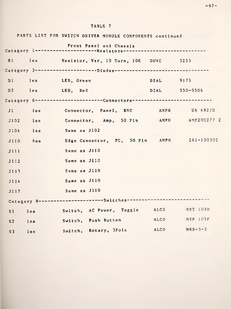
TABLE 7
PARTS LIST FOR SWITCH DRIVER MODULE COMPONENTS continued
Front Panel and ChassisCatagory 1 “---Resistors
R 1 lea Resistor, Var, 10 Turn, 10K DUNC 3253
Catagory 3 --- Diodes
D 1 lea LED, Green DIAL 9173
D 2 lea LED, Red DIAL 550-0506
Catagory 6---
J1 lea Connector, Panel, BNC AMPH U 6 492 /U
J 1 0 2 lea Connector, Amp, 50 Pin AM PH AMP 2 00 2 7 7 2
J 104 lea Same as J 1 02
J 1 10 6 e a Edge Connector, PC, 50 Pin AMPH 261-100302
Jill Same as J 1 1
0
J 1 1 2 Same as J 1 1
0
J1 13 Same as J 1 1
0
J1 14 Same as J 1 1
0
J 1 1 7 Same as J 1 1
0
Catagory o
S 1 lea Switch, AC Power, Toggle ALC0 MST 105D
S 2 lea Switch, Push Button ALCO MSP 1 05F
S3 lea Switch, Rotary, 3Pole ALCO MRB-3-3

TABLE 7
PARTS
Satagory
U
i tagory
itagory
itagory
LIST FOR SWITCH DRIVER MODULE COMPONENTS continued
Front Panel and Chassis
9 Meters
lea Meter, Panel, 0 Center, 1 . 5Ma MODT 25DMA1.5U
10 Hardware
Plate, Front Panel 7"X9" BUD 91F36
Card Cage SCBE 60047A
10
Hardware —Fuseholder Littlefuse 342001
11
Miscellaneous
Power Supply 5V, 1A Standard SPS/15

- 99 -
ACKNOWLEDGMENTS
The existence of this measurement system is the result of a
joint effort involving cooperation of many people over a long
period of time. These include: Gerome Reeve for the original
system design, Lanny D. Driver for development of the ambient
and cryogenic coaxial standards, Lanny D. Driver and David F.
Wait for the original software model, John P. Wakefield for the
switch driver module design and software tie-in, and William
Daywitt who was largely responsible for the theory, error
modeling, and analysis.

- 100 -
REFERENCES :
[1] Larsen, N.T.; NBS Type IV Power Meter Operation and Maintenance
Manual; NBSIR 77-866, Oct. 1977.
[2] Larsen, N.T.; A New Self-Balancing D.C. Substitution RF Power
Meter IEEE Transactions on Instrumentation and Measurement;
Vol. IM-25, No. 4, pp. 343-347, Dec. 1976.
[3] Miller, C.K.S., Daywitt W.C.,and Arthur M.G.; Noise
Standards, Measurements, and Receiver Noise Definitions;
Proceedings of the IEEE, Vol 55, No. 6, June 1967.
[4] Wait D.F.; Earth Terminal Measurement System Operations
Manual; NBSIR 78-879, April 1978.
[5] Wakefield, J.P.; Earth Terminal Measurement System
Maintenance Manual; NBSIR 78-895, April 1978.

- 101 -
APPENDIX I
PROGRAM LISTING AND VARIABLE CROSS REFERENCE TABLE
This is a listing of program "30M20" arranged to allow easy
reference to the main program and associated subprogram segments.
Each segment listing is followed by the cross reference table for
the variables referenced. Except for frequency dependent program
constants, this program listing is identical to that for "60M20".
Line numbers referenced for variables apply to both programs.


1 SEPT 198130M20
- 103 -
1 ! THIS VERSION IS JULY 101 981 VS10 ! 30RBD20 ! 30RAD 30 MHZ CONSTANTS IN THIS VERSION30 ! RE-STORE "30M20" ! MARCH26 1981 110031 !
32 !
33 !
34 !
35 !
40 OPTION BASE 1
50 COM File, Flag60 COM 06 , 07 , 08 , Q9 ,
R2,R3
,L
,R
,A6
,A?
,AS
, A9 , Z 1 ,1 2 ,
N3,N8
,N
,F
,FO
,W
70 COM SHORT F < 4 > , L < 8 , 20 > , M < 32 , 33 > , H < 26 , 1 1
)
SO COM II# C80],F‘#[ 100] ,
INTEGER D < 6 , 75 > ,NO
,X# [ 80 ]
90 COM C#C 1003 , G#C 1003 , Rf [ 1003 , B#C 103 , H#[ 1003 , Q#C503 , V#[ 1003100 COM ATI 100] , Z2,Z3,Z4,Z5,T1,S1, T4 , T2 , T3 , Z6 , F7 , T7 , T8 , T9 , P9 , X6 , X7 , X8 , X91 1 0 COM Q 1 , 02 , 03 , 05 , E2, ZU , 1 00 ) , B5 , B6 , B7 , B8 , C 1 , R5 , PI , P2 , P3 , P4 , V2 , Pout $
1 20 COM P 5 , P 6 , P 7 , PS , U 1 , W2 , W3 , W4 , W5 , W6 , T5 , T6 , E7 , J8 ,I 6 , S , I 5 , X3 , P0 , I , C2 , M i
s
130 COM Real, I mag140 DIM Z$C100]150 P t e s t = 0
160 I pause = 0
170 FOR K= 1 TO 5
171 ! 0 = F N T < Q
)
172 ! 0=FNK<3>173 Q=FNData<Q>174 GOTO 220180 Q = F N P < Q >
190 PRINTER IS 16
2O0 PRINT P1*1000,P2*1000,P3*1000210 Ptest =F't. est +P1220 NEXT K
230 Pl=Pt- est..-'(K-l >
240 PRINT "AVERAGE POWER AT PORT 0 IS " ; P 1 * 1 000 ;" M I LL I WATTS
"
250 PAUSE251 MASS STORAGE IS ":F8,1"260 Cl = . 99949 ! THIS IS ALPHA OF GR9O0-N ADAPTER270 C2=. 00010 ! THIS IS UNCERTAINTY OF THIS ADAPTER ALPHA280 R 5 = 1
6
290 H# [ 1 , 103=" GR90O •
N
"
300 H t C 1 1 , 203 = " 47.0 + JO0.0"310 R e a 1 = 4 7
320 Irnag=. 00001330 Printer=0340 F i 1 e = O + . 1
5
350 PRINTER IS 0
360 PRINTER IS 16
370 ! CREATE " NF I LE :F8
" , 40380 ! ASSIGN #1 TO "NFILE"390 ! PRINT #1 ; N<*> , END400 ! ASSIGN # 1 TO *
410 ASSIGN #2 TO "NFILE"420 READ #2;H<*>430 ASSIGN #2 TO *
440 MAT PRINT N
450 PRINTER IS 16
460 DISP "STOP— CHECK N MAT PRESS CONT TO GO ON"
470 ! PAUSE480 Z$ =
" 30 -'60 MHZ AUTOMATED NOISE MEASUREMENT SYSTEM <D 1-M -4XT1-T1 >"
490 V#= " EXECUT I VE PROGRAM VERSION GJC 2-45 MAR 81 ETMS #6.11"
500 PRINT TAB<15>, Z*
510 0 =FNSU)
m at c h

- 104 -
520530540550560570580590600610620630640650660670630690700710720730740750760770780
PRINT TAB < 7 > , V$Q =FNS < 4 >
PRINT "ENTER flLPHR FOR CONNECTOR-"ADAPTOR COMBINATION USED ON UNKNOWN PORT"C 1 =FNN < C 1
>
PRINT "ENTER UNCERTAINTY FOR ADAPTER COMBINATION USED"C 2 = F N N C C 2 >
Q=FNS< 1
>
P#=H$C 1 ,10]12 = 2
PRINT "ENTER ADAPTER USED TO CONNECT DEVICE UNDER TEST"Q = F N 0 < 1 >
H$ [ 1 , 10]=PJQ=FNS< 1
>
P$=H$[ 1 1 , 20]PRINT "ENTER REAL AND IMAGINARY SOURCE IMPEDANCE IN THIS FORM"Q =FNO < 1
>
H$ [ 1 1 , 20 ] =F't
PRINT "ENTER REAL PART OF THE SOURCE IMPEDANCE"Real = F N N Real )
PRINT "ENTER THE IMAGINARY PART OF THE SOURCE IMPEDANCE"I mag=FNN < I mag >
PRINT C 1 ; C2 ; Ht C 1 , 1 0 ] ; Hf C 1 1 , 20 ] ; Real ; I magF = 3 0
K9 = 0
Q5 = 1 0000D9= 1
790 Z 8 = 0
800 PRINT T A B ( 7 > , V $
810 Q = F N S < 4 >
820 ! OUTPUT 9; "SI 1 , 04, 09, 35, 50"! RESET TIME HERE
830 OUTPUT 9;"R"840 ENTER 9;P$850 PRINT TAB<15),P$; " : 1981"860 Q = FNS < 2 > + FNE < 0 > +FNE < 1
>
870 IMAGE "IF HARDWARE HANGS UP ", -'V' ,"< 1 > STOP + STOP 2 > KEY0 3 > 0 RESTRT"880 ! PRINT USING 440890 Q=FNGK1)900 G = F N Q < 1 0
)
MAIN
Cl *
C2 *
D9 780
F *
File *
HJ *
12 *
I mag *
I pause 160
K 170
K9 760
N < *
260 550 550 730
270 570 578 730
740
340
290 300 590 630
600
320 720 720 730
220 230
650 680 730 730
420 440

- 105 -
Pf * 590 630
PI * 200 210
P2 * 200
P3 200
P r i n t e r 330
Pt € £ t- 150 210 210
Q678 810
173860
173890900
180
Q5 * 770
R5 * 280
Real * 310 700
V$ * 490 520
Zt 140 480 500
*7 750
28 790
680 840 850
240
510 530 580 620 640
730
650
23©
230
180
700
800

- 106 -
9109209309409509 6 0
970980990
DEF FHCKQ)OPTION BASE 1
f nt.1 Cl !; Cl in
COM1 0 0 0 COM P 5 ,
P 6 ,P 7 ,
F'8,M 1 ,
U2,M3
,M4
,M5
,N6
,T5
1010 C 0 M Real,
I rn ag1020 B r ari c h = Q
1030 PRINT 0
1040 0 H B r an c h GOTO 12 8 0, 13 0 8 ,1 300, 2380,
1
1 050 IF < B r an c h > = 1 ) A N D < B r ari c h < — 1 0 THEN10,1 340, 2400, 1350, 13701060 RETURN 0
1070 FNEHIi1080 GOTO 11101 0 9 0 Z 1 = Z 2 = Z 3 = Z 4 = Z 5 = Z 6 = 0
1100 F 1 ag (. 5 > =01110 REM THIS IS THE MAIN TRAP1120 0 = F N B C 2 >
1130 0 = F H S ( 1 )
1 140 K 6=11150 REM NOISE SOURCE CALIBRATION1160 Z1=01 170 Q = FH J ( 1 > + FN J < 2 > +FN J < 3 >
1 180 GOTO 12301 190 Z 2 = 0
1200 0 = F N J ( 2 >
1210 GOTO 11201220 Z 3 = 0
1 230 0 = F H K < 0 > + F H K < 1 > + F N K < 2 > + F H K C 3 > + F N C h e c k
1240 PRINT "END OF MEASUREMENT SEQUENCE -
1250 PAUSE1 260 GOTO 3101270 RETURN 0
1280 ! CONTINUE1 290 RETURN 0
1 300 PRINT "CONNECT UNKNOWN TO PORT" ; Q71 3 1
0
PRINT "CONNECT AMBIENT TO PORT" ; Q81320 PRINT "CONNECT STANDARD TO PORT " ; Q91 330 RETURN 0
1 340 ! CONTINUE1 350 ! CONTINUE1360 RETURN 01370 ! CONTINUE1 380 RETURN 0
1 390 FNEND
FNQ <.
t?0
13
Br anc
h
F 1 ag <
Kb
Q
07
08
1020 1040 1050
1 1 00
1140
910 1020 1 0 3
0
* 1300
1 0 5
0
105 0
1060 1120 1130 1170
, X7, X8, X92 , Pout $
, I ,C 2 ,
M i smat c h
,1090
00, 1300,2380, 13
1200 1230
1310

- 107 -
Q9 1 320
Z1 & 1090 1 160
22 * 1090 1 190
23 1090 1220
24 * 1090
25 *• 1 090
26 1090
- 108 -
1400 DEF FNE<0)1410 OPTION BASE 1
1420 COM F i 1 e , F 1 ag1430 COM 06, 07, 08, 09, R2, R3, L, R, R6, R7, AS, R9, Z1 ,
12, N3, N8 , N , F , F 0 ,
W
1440 COM SHORT F < 4 > , L < * > , M < 32 , 33 > , N < 26 , 1 1 >
1450 COM D# C SO 3, Pf Cl 00], INTEGER D < 6 , 75 > ,NO , X* C SO 3
1460 COM C$ C 1 00 3 , Gt C 1 0O 3 , R# C 1 00 3 , Bt C 1 0 3 , H$ C 1 0O 3 , Q$ C 50 3 , V* C 1 00 3
1470 COM A*C1003,Z2,Z3,Z4,Z5,T1,S1,T4,T2,T3,Z6,F7,T7,T8,T9,P9,X6,X1480 COM 01 , 02, Q3,Q5,E2,Z<1, 100), B5, B6, B7, B8, Cl ,
R5, F'l,P2, P3, R4, V2
1490 COM P5 , P6 , P7 , P3 , W 1 , W2 , U3 , W4 , W5 , W6 , T5 , T6 , E7 , J8 , 1 6 , S , 1 5 , X3 , PO
,
15O0 COM R€a1,Imag1510 IF Q THEN 15801520 REM THIS INITIALIZES THE HARDWARE <FNE0>
7 ,X 8 ,
X 9
,Pou t
t
I , C2, Mi
i
1530 F1ag<l>=01540 F 1 ag < 5 ) =01550 Q=FNQ<8>1560 PRINT "HARDWARE INITIALIZED"1570 RETURN O
1580 REM THIS INITIALIZES THE SOFTWARE < FNE 1
)
1590 Q = I = N =
N
3 = N 8 = F' = L 0 = F 0 = I O = 1 1 = 1 2 = K 6 = Z 1 = Z 2 = Z 3 = 0
1600 07=01610 08=11620 09=21630 R7=R8=A9=61640 PRINT "SOFTWARE INITIALIZED"1650 RETURN 0
1660 FNEND
FNE':
A7 * 1630
A8 * 1630
A9 * 1630
FO * 1590
FI ag< 1530 1540
I * 1590
10 1590
1
1
1590
12 * 1590
K6 1590
L0 1590
N
N3
N8
P
0
07
1590
1590
1590
1590
1400 1510 1550 1590
=• rn at c h
1600

109

-no
1670 DEF F H J <
Q
> !KFNJ>1680 OPTION BRSE 1
1690 COM File, Flag1700 COM Q6 , 07 , 08 , 09 , R2 , R3 , L , R , AS , R7 , AS , R9 , Z 1 ,
I 2 , N3 , H8 , N , F , F 0 ,
W
1710 COM SHORT F < 4 > , L < * > , M < 32 , 33 > , N < 26 , 1 1)
1720 COM Dt C 80 ], PtC 100] , INTEGER D<6 , 75 ) , N0, X* C88
3
1 730 COM Cf C 1 00 3 , Gt C 1 00 3 , R* C 100 3 , B* C 1 0 3 , H* C 1 00 3 , Q* C50 3 , V» C 1 00
3
1740 COM fl* E 1003 , Z2, Z3, 24, Z5, T1 , SI , T4, T2, T3, Z6, F7, T7, T8, T9, P9, X6,1750 COM Q 1 , Q2 , Q3 , Q5 , E2 ,
Z < 1 ,1 00 > , B5 ,
B6 , B7 , B8 ,C 1,R5,P1,P2,P3,F'4,V«
1 760 COM P5 , P6 , P7 , P8 , W 1 , N2 , M3 , W4 , M5 , M6 , T5 , T6 , E7 , J8 , 1 6 , S , 1 5 , X3 , P0
,
1770 COM Real, I mag1780 Branc h = Q
1790 ! CONTINUE180O IF < Branc h<=l> RND < Branc h< =4 > THEN ON Branch GOTO 1810,2470,1810 IF Z 1 =2 THEN 24701820 Q = F N S < 2 >
1 8 3 0 PRINT " C U S TOME R ? < 0 = B V , S P = N C >"
;
1840 Pt=C$Cl,2931850 IF 12=0 THEN 1920i860 nisp "NOW: ";P$;1870 L INPUT 0t1880 IF Q $ = " 0 " THEN 24301890 IF Qt=" " THEN 19801900 CtCl,29]=0t1910 GOTO 19901920 II ISP "NOW: ";F>t1930 I 0 = F N B < 2 : +FNS < 1 > + FNW < 50 >
1 94019501 9 6 0
1 97019801 9902000201020202 0 3 0
20402 0 5 0
20602070208020902 1 0 0
2 1 1
0
2 1 2021302140215021602170218021902200221022202230224022502260227022802290230O
L INPUT QtIF Qt="0" THEN 2430IF Q t = " " THEN 1980CtC 1 , 29]= 0
t
Q = F N S < 1 >
PRINT "GUST'S ADDRESS— STREET ?";Pt=CtC30, 693Q = F N 0 < 1 >
CtC 30, 6 9 3 = P
t
0 = F N S 1 >
PRINT "GUST'SP t = C t C 7 0 , 99 3
Q = F N 0 < 2 >
CtC 70, 9 9 3 = P t
Q=FNS< 1
>
PRINT "SOURCEPt=GtC 1,393Q = F N 0 < 3 )
GtC 1 , 3 9 ] = P t
Q = F N S ( 1 >
PRINT "SOURCEPt=Gt C40, 79]0=FNO<4>GtC40, 79] =PtQ = F N S •'
1 >
PRINT "SOURCEPt=GtC80, 89]Q = F N 0 < 5 >
GtC 80, 89]=PtQ=FNS< 1
>
PRINT "SOURCEPt=GtC90, 99]G=FN0<6)GtC 90, 99]=PtQ = F N S 1 >
ADDRESS?—CITY, STATE, ZIP
MRHUFTR? "
;
TYPE ?
MODL # ?";
SEP. # ?";
PRINT "DATE OF CALIBRATIONPt=RtC 1,19]
iX 7 ,
X 8 ,^*1 9 1 2
: ,Pout, t
iI , C2 ,
M i e mat
2 6 8 0

- 111 -
2310 Q=FN0<7>2320 RiC 1 , 1 9 3 = P$2330 Q =FHSd>2340 PRINT " C ft L I B . TEST # ?";2350 P*=R$[20,3932360 Q = FN0 ( 7 >
2370 Rf [ 20 , 39 3 =P$2380 Q=FNS ( 1 )
2390 PRINT "REQ OR REF # ?
240O P$ = Rt [ 40 , 69 3
2410 Q=FNG(9)2420 R$C40,693=P*2430 12=12440 21=21+12450 Q = FNS(2> + FNB< 1 >
2460 RETURN 0
2470 REM GET PARAMETERS SUBROUTINE <FNJ2>2480 IF 22 THEN 26802490 Q = FNS < 2 )
2500 ! BISP "NUMBER OF FREQUENCIES DESIRED ?";2510 F0=
1
2520 ! DISP "NUMBER OF LEVELS PER FREQUENCY ?";2530 L 0=
1
2540 FOR 10=1 TO F02550 F < I 0 > =F2560 NEXT 102570 Q=FNS(1>2580 P$=" ENTER VALUE OF ATTEN A2"2590 PRINT Pf26O0 R5=FNN<R5>2610 P*=" LEVEL SETTING A2="2620 N3=52630 N8=52640 2(1,51 >=R52650 22=12668 Q=FNS(2)+FNB( 1
>
2670 RETURN 0
2680 REM PORT ASSIGNMENT SUBROUTINE (FNJ3)2690 IF 23=1 THEN 28102700 Q = F N S ( 2
>
2710 PRINT "****HORMftL PORT ASSIGNMENTS****"2720 Q =FNS < 2
)
2730 Q7=02740 PRINT "UNKNOWN CONNECTED TO PORT" JQ72750 Q8 = 32760 PRINT "AMBIENT CONNECTED TO PORT" ;qs2770 Q9=22780 PRINT "STANDARD CONNECTED TO PORT" ;Q92790 Q = FNS < 2
>
2800 23=12810 Q=FNS ( 2 > + FNB ( 1
>
2820 RETURN 0
2830 FNEND
FN J (
Branc h >-» 00 o 1800 1800
C t * 1840 1900
F * 2550
F ( * 2550
1800
1970 2000 2020 2050 2070

- 112 -
F0 * 2510 2540
G* * 2100 2120 2150 2170 2200 2220 2250 2270
10 1930 2540 2550 2560
12 * 1850 2430
L0 2530
N3 * 2620
N8 * 2630
P$ * 1840 I860 1920 2000 2020 2050 2070 2100120 2150 2170 2200
2220 2250 2270 2300 2320 2350 2370 2400420 2580 2590 2610
0 1670 1780 1820 1980 2010 2030 2060 2080 212130 2160 2180 2210
2230 2260 2280 2310 2330 2360 2380 2410450 2490 2570 2660
2700 2720 2790 2810
0$ * 1870 1880 1890 1 9 0 0 1940 1950 I960 1970
Q? * 2730 2740
Q8 * 2750 2760
Q9 * 2770 2780
Rt * 2300 2320 2350 2370 2400 2420
R5 * 2600 2600 2640
Z< * 2640
Z1 * 1810 2440 2440
Z2 * 2480 2650
Z3 * 2690 2800

- 113 -
284028502860287028802890290029102920293029402950296029702980299030003010302O3030
DEF FNK<Q) ! ! ! < FHK0
>
OPTION ERSE 1
COM F i 1 e , F 1 agCOM Q6,Q7,Q8,Q9,R2,R3,L,R,R6,R7,R8,R9,Z1 , 1 2 , N3 , N3 , N , F , F0 ,
WCOM SHORT F<4),L(*),M(32,33),N<26,11)COM Df [803 , P$C 1O0] , INTEGER D < 6 , 75 ) , N0 , X* C 80
]
COM C#C 100] , GtC 100] , RtC 100] , Bf C 10] , H$C 100D , Q$C50] , Vf C 100]CON R$C 100] ,Z2,Z3,Z4, Z5,T1 , SI , T4 ,
T2, T3, Z6, F7, T7, T8, T9, P9, X6, X7, X8, X9COM Q 1 , Q2 , Q3 , 05 ,
E2,Z < 1 ,
1 08 > ,B5
,E6
,E7
,B8
,C 1 , R5 ,
P 1 ,P2
,F'3
,P4
,V2 ,
Pour t
COM P5,P6,P7,P8,W1, W2, W3, W4, W5, W6, T5, T6, E7, J8, 1 6 , S , 1 5, X3, P0 , I ,C2
,M i srnat c
h
COM Real , I magB r an c h= Q +
1
ON Branch GOTO 2980,3310,3920,5520! !
i FREQUENCY SUBROUTINE ( FNK0
)
FOP F9= 1 TO F0F = F < F9 )
Q = FNL < 1 )
L0= 1
10 = 0
FOR I 1 =F9*L0-L0+ 1 TO F9*L03040 10=10+13050 M< I 1 ,
1 )=F3060 M < I 1 , 2) = I
1
3070 M < I 1 ,3) =L(I0, 1
>
3080 M(I1,4)=L(I0,2)3090 M< I 1 , 5)=L(I0, 7>
3100 M < I 1 , 6)=L< 10, 8)
3110 MCI 1 , 7)=L< 10, 3>
3120 M< 1 1, 8> = L< 10,4)3130 M< 1 1 , 9)=L< 10,5)3140 M < I 1 ,
10> = L< 10, 9>
3150 M< I 1 , 1 1 > = L< 10, 10>
3160 M < I 1 , 1 2 ) = L< 1 0 ,1 1
>
3170 M<I 1 , 30>=L< 10, 6)
3180 M< I 1 , 31 >«L< 10, 12)3190 NEXT II
3200 NEXT F93210 T2=(M< 1 , 3)+M<l , 5>>/23220 T3= < M < 1 , 4 ) +M < 1 , 6 > ) ''2
3230 T 1 = < M Cl , 7 ) +M <1 , 1
0
) ) '2
3240 Z<1,52)=T13250 2<1,53>=T23260 Z< 1 , 54 > = T33270 Q =FNS ( 4 )
3280 Z4=
1
3290 Q=FNS(2)+FNBC 1
)
3300 RETURN 0
3310 i m NUMBER CRUNCHER SUBROUTINE F N K 1 >
3320 L0=
1
3330 F0= 1
3340 R9=F0*L03350 FOR 19=1 TO R93360 T8=B8+B73370 T1 = <M<I9,7)+M<19, 1 0 > ) /
2
3380 M < I 9 , 1 3 ) =T
1
3390 N=N8*N3*23400 N 9 = H
3410 T7=B5+B63420 TS=T8*T8/N3430 S 1 = < T7-T8 ) / < N- 1
)
3440 S 1 =SQR < S 1
>
3450 M < 1 9 , 14 ) =S 1 /SQR ( N )
3460 M<I9,23>=S1/SQR<H>3470 T4=<M< 19, 9)+M< 19, 12) )/2

- 114 -
3480 MCI'?, 1 5 > = T 4
349Q T2 = < M C I 9 , 3 ) + M < 1 9 ,
5
) ) /23500 M < I 9 , 1 6 > = T 2
3510 T3=CMC 19, 4>+MC 19, 6> >/23520 MC 19, 1 7 ) =T33530 R 8 = C T 1 - T 2 > C T3-T2+ 1 E-6 >
3540 ! !!!!!!!!!!!!!!!!!!!!!!!! ! TEMP IS FOR 30 MHZ NC14,9>3550 M C I 9 , 2 3 > = A B S C 1 - R 8 > * N < 1 4 , 9 )
3560 M C 1 9 , 24 ) =ABS < R8 > *N < 1 2 , 1
)
3570 MC 19, 32>=MC 19, 38>+M< 19, 31 >/2
3580 G=MCI9,32>3590 ! I!!!!!!!!!!!!!!!!!!!!!!!!!!!!!!!!!!!!! ! BANDWIDTH W IS FOR 30 MHZ3600 W = . 7 7 3
3610 Q = H C 1 2 , 9 > W/ C T2 + T4 >
3620 M C 1 9 , 33 > = 1 0*LGTCQ
>
3630 Q = . 0 0 2 3
3640 QO= 1+ZC1, 16> f'Z Cl, 52 > !1+ TE'TX3650 Q 1 = 1 - Z C 1 , 5 3 > / Z C 1 , 5 2 > ll-TR/TX3660 G 2 = C Z C 1 , 54>+Z< 1 ,
16) )/(Z( 1 , 54>-ZC 1 ,53) > ! TS+TE'TS-TA
>
3670 Q3=ZC 1 , 52>*CG0-Q1*G2>3680 M C 1 9 , 2 5 > = Q * Q 3
3690 MC 19, 26>=N< 10, 1 >*10MMC 1 , 33)^ 18>*NC 10, 2>*<T1-T3)*CT1-T2>3700 Q=T2- T1+ABSCC1-T2/T1 )/< l-T3/T2)+lE-6>3710 Q=ABSC1-T2/T1>+1.7*Q3720 ZC 1 , 57>=N< 12, 8)3730 ZC 1 , 55>=NC 12, 7)3740 Q3=T1*T3+T1*T2+T3*T23758 03=03/ CT3-T2)3760 03=ABSC03*NC 12,
8
)
>
3770 MC 1 , 2 9 ) = Q 3
3780 Q = M C 19, 2 3 > + M C 19, 24)+M< 19, 25)3790 M C I 9 , 1 8 > =Q + M C 1 9 , 26 > +M C 1 9 , 29 >
38O0 MC 19, 19>=3*MC 19, 28)38 1 0 M <19, 20 > =M < 1 9 , 1 8 > +M < 1 9 , 1 9 >
3820 MCI 9, 21 > = 18*LGT CABS C CT1 -290+1 E-6 >'290> >
3830 Q2= C MCI, 19)+M<1, 1 8 ) > ^ C T 1 -290
)
3840 G3=RBS C 1 +Q2
)
3850 M C 1 9 , 22 ) = 1 0*LGT C 03 >
3860 M C 1 9 , 32 > = < M < 1 9 , 38 ) +M C 1 9 , 3 1 > ) /23870 NEXT' 193880 25=
1
3890 Q=FNB < 2 >
3980 RETURN 8
3910 ! FNK23920 0 = F N V s w r C 0 >
3938 PRINTER IS 83940 Z C 1 , 26 > =M i s mat c
h
3958 E7=MC 1 , 18)+Mi smatch3960 E 6 = 1 - 1 / Cl3970 E 1 = E 6 * C E 7 / M C 1 , 13))3980 E2=E6*. 00053990 C9=C 1 *C
1
4800 E8=CMC 1 , 1 3 > - M C 1 , 3) VC9*CC2/Tl
)
4018 E3=AB3CE1)+ABSCE2) +ABSCE0)4028 E3=ABSCE3)4030 VT= "*=*=*=*=*=*=*=*=*=*=*=*=*=*=*=*=*=*=*=*=*=*=*=*=*=*=**=*=*=*=*=*=*=*=*"4040 L0=
1
405O ! PRINT V#4060 18=04870 FOR 19=1 TO F04080 FOR J 9 = 1 TO L84090 18=18+14100 0 1 =FNS C 3
)
4118 PRINT Z$4120 At = M "

- 115 -
4130 Q1=FNS<1)4140 N9=N3*NS*24150 ! PRINT PAGE4160 PRINT TAB < 6 ) , A$4170 Q=FNS(10)4180 PRINT TAB<23); "MEASUREMENT RECAP"4190 PRINT TAB<30) ; "AND"42O0 PRINT TAB<22); "PRELIMINARY RESULTS"4210 Q = FNS < 5
)
LEVEL SETTING OF A2=";R54220 PRINT TAB<6); "FREQUENCY=" ; MCI , 1); "MHZ"4230 PRINT TAB<6>; "SOURCE I MPEDANCE " ; H$ [ 1 1 , 20 3
,
"
4240 PRINT TAB<6);A*4250 PRINT TABC10); " TA " ; TAB < 20 )
, "R OHMS" ; TAB<34> ; "TS" ; TAB<45) J "R OHMS"4260 PRINT T A B < 6 ) ;
" "
4270 FIXED 2
4280 PRINT TAB <8>;M<lf 3>;TAB<20>;Z<l,59>;TAB<32>;M<I f 4>;TAB<45>;2< 1,60);
"
; " 1 ST 50 MEASUREMENTS"4290 PRINT TAB<8>;M<l,5>;TAB<20>;Za,59>;TAB<32>;M<l f 6>;TAB<45>;Z<1,60>;
"
; " 2ND 50 MEASUREMENTS)"4300 PRINT TAB(6);A$4310 PRINT TAB(ll); " TX " ; TAB < 2 1 )
;" SX " ; TAB < 34 )
; "TE"4320 PRINT T A B < 6 ) ;
11
4330 PRINT TAB<8>;M<1,7);TAB<20>;M<1,8>;TAB<32>;M<1,9>;" "< 1ST 50 MEASUREMENTS)
"
4340 print tab<6);m<i,10);tab<20>;m<i,ii>;tab<32>;m<i,12>;" ";"<2ND 50 measUREMENTS)"4350 PRINT4360 PRINT TAB<6);A$4370 PRINT4380 STANDARD4390 N9=N8*N3*24400 PRINT TAB < 6 )
;" AVE POWER IN MILLIWATTS P1,P2,P3"
44 10 PRINT TAB (6) ; Z(1 , 45 ) -'N9* 1 000 J Z < 1 , 46)'N9*1000; Z< 1 , 47)/'N9*10004 420 S1=SQR< <Z< 1 , 48)-Z< 1 , 45)*Z< 1 , 45)/N9)/'<N9-l ) )
4 430 S2 =SQR< <Z(1 , 49 > -Z <1 , 46 ) *Z < 1 , 46)/N9),'<N9-l ) )
4440 S3=SQR< <Z< 1 , 50)-Z< 1 , 47>*Z< 1 , 47)/N9)/'<N9-l ) )
4450 2 < 1 , 3 1 ) =N94460 PRINT TAB<6>; "SD P1,P2,P3 C# OF MEAS=" ; Z< 1 , 31 )
;"
3" ; SI ; S2; S3
4470 PRINT TAB<6) ; At4480 Q=FNS<20)4490 ! PAGE4500 PRINT USING 4520;M<I8,1)4510 Z(1,34)=M(1, 1)
4520 IMAGE 25X ," FREQUENCY =" , M3D. D, "MHZ"
4530 PRINT4540 PRINT Z t
4550 G1=FHS<1>4560 E4=100*E3'M<1, 13)
4570 E5 = E3 + Mi sh.atch
4580 M2=100*<M1/M(1 , 13)
)
4590 M5=E4+M24600 MU , 13) = M< 1 ,
18)+E54610 PRINT USING 4620; M < 1 3, 1 3 ) , M< 1 8, 1 8 ) , M< 18, 1 9)
4620 IMAGE 10X, "NOISE TEMPERATURE «",M5D.2D,"K + -" , M3D . 2D ,
" K < B I AS ) +-",M3D.2D,
K <3*SEM>"4621 Q2=(M< 1 , 18)+M< 1 , 19) )/<Tl-290)4622 Q3 = ABS < 1 +Q2
)
4623 M< 1 , 22)=10*LGT<Q3)4630 Z< 1 , 35)=M( 1 , 13)
4640 Z< 1 , 36)=M< 1 , 18)
4650 Z<1, 13)=M<1, 19)4660 IF T 1 < 220 THEN 46904670 PRINT USING 4680 ; M < 1 8 , 2 1 ) , M < 1 8 , 22
>
4680 IMAGE 10X, "EXCESS NOISE RATIO=" , M3D. 2D , "DB -",MD.2D ,"DB<BIAS + 3*SEM'>"
4690 Q 1 =FNS < 1
)

- 116 -
4760 Z(l, 14)=M( 1 , 21
)
4710 Z(1 , 15)=M( 1 , 22
>
4720 PRINT USING 4730; M( IS, 15) , 10*LGT < 1+M< 18, 15)^290
>
4730 IMAGE 1 0 X, "RADIOMETER SYSTEM TEMPERATURE = ",4D , "K <
" , 4D. D, "DB NF )"
4740 Z< 1 , 16)=M< 1 , 15)4750 Z<1 ,
1 7 > = 1 0 * L G T ( 1+M( 1 ,15)^290)
4760 PRINT USING 4770; M( I 8 , 33)4770 IMAGE 1 0X , "RADI OMETER GAIN = " , M4D.1D ,"BB"4780 Z < 1 , 56 ) = . 7734790 PRINT " RADIOMETER NOISE BANDW I DTH= " ; Z < 1 , 56 >
; "MHZ
"
4800 Z< 1 , 18) = M( 1 , 33)4810 Q 1 = F N S ( 3
)
4820 PRINT TAB (28), "ERROR SUMMARY"4830 Q 1 = F H S ( 1 )
4840 PRINT TAB ( 5 ), "SOURCE OF ERROR";TAB < 35) ,
" SOURCE"; TABC58) , ERROR IN"
4850 PRINT TAB C 34 ), "UNCERTAINTY" ; TAB<55) , "NOISE TEMPERATURE"4860 ! CONSTANTS FOR TEMP ARE 30 MHZ4870 Q 1 =FNS ( 1
)
4880 PR I NT US I NG 4890 ; N < 1 2 , 1 ) ; 1 00*M (I 8 , 24 ) /M <1 8 , 1 3 >
4890 IMAGE 6X, "CRYOGENIC STANDARD", 10X,MZ.2D, "K" , 16X, M4D. 2D4900 Z< 1 , 19)=N( 12, 1
>
4910 Z Cl,20 ) = 1 00*M ( 1 , 24 ) .•"M ( 1 , 1 3 >
4920 PRINT USING 4930; N< 14, 9) , 108*M< 18, 23)/M< 18, 13)4930 IMAGE 6X, "AMBIENT STANDARD" , 12X, MZ. 2D, "K" , 16X, M4D. 2D4940 Z< 1 , 21 )=N< 14, 9)4950 Z < 1 , 22 ) = 1 0O* M < 1 , 23 ) •-"M < 1 ,
1 3 )
4960 PR I NT US I NG 4970 ; N ( 12,3 ) ,1 00*M < I 8 , 25 > -'M ( 18,13)
4970 IMAGE 6X, "POWER RAT 10
" , 1 7X , MZ . 2D , " DB " , 1 5X , M4D . 2D4980 Z(1 , 23)=N( 12, 3)
4 9 9 0 F' R I N T IJ S I N G 5 8 0 6 ; 1 8 0 * M i & m at c h M ( 13,1 3 )
5000 IMAGE 6X, "MISMATCH" ,21X, "0.5R; 1 .0J OHMS " , 7X , M4D . 2DSO 10 Z ( 1 , 26 > = M i £ mat c
h
5020 Z '1 , 24 > = 1 08 *M ( 1 , 25 ) -- M < 1 , 1 3 )
5030 PR I NT US I NG 5060 ;N (10,3), 1 00*M ( I 8 , 26 ) /'M < 1 8 ,
13)5040 Z(1,27)=N(12,4)5050 Z (1 , 28 ) = 1 00*M C 1 , 26 ) /M <1,13)5060 I MAGE 6X
," NONL I NEAR I T Y " , 1 6X , M 1 D . 2DE , 1 2X , M5D . 2D
5070 PR I NT US I NG 5080 ; Z < 1 , 55 ) , 1 00*M < I 8 , 29 ) .'M (18,13)5080 IMAGE 6 X ,
"SWITCH ASSYMETRY", 12X,MZ.3D, "DB", 12X,M6D.2D5090 Z < 1 , 29 > = 1 00* M ( 1,29) /M (18,1 3
)
5110 Adapt e r= 1 00*E3^Z( 1 , 35
)
5120 PRINT USING 5 1 30 ;Hf C 1 ,
1 0 ] ,1 00*E3.-"Z ( 1 , 35 )
5130 IMAGE 6 X, "ADAPTER: " , 18A, 1 IX, "0. 000 IBB" , 1 IX, M6D. 2D
5140 PRINT TAB (6), A*5 1 50 PR I NT US I NG 5160; 1 00*M (18,18 )
- M ( 1 8 , 1 3
)
5160 IMAGE 6X, “LINEAR SUM OF BIAS ERRORS ", 24X , M5D . 2D5170 Z ( 1 , 30 ) = 1 00*M ( 1 ,
1 8 ) -- M (18,13 )
5180 PR I NT US I NG 5 190; N9 ,1 00*M (18,19 ) /M (18,13)
5190 IMAGE 5 X,
" 3 * S T A N D A R D ERROR OF MEAN ( « ME AS = " M3D .,")", 1 0X , M4D . 2D5200 Q= 1 00*M <18, 18) /'M <18, 13)5210 Q 1 = 1 00*M (18, 19 ) /M (18,13)5220 M( 18, 20)=Q+Q15230 Z < 1 , 3 1 ) = N
5240 Z < 1 , 32 ) = 1 00*M <18, 19) /'M <18, 13)5250 PRINT T A B ( 6 ) , A $
5260 PRINT USING 5270 ; M ( 1 8 , 20
)
5270 IMAGE 6X, "LINEAR SUM OF ERRORS" , 31 X, M3D. 2D5280 Z( 1 , 33)=M< 1 , 20)5290 Q 1 = F N 8 ( 1
)
5300 PRINT TAB (6), At5310 NEXT J
9
5320 NEXT 195330 PRINT5340 PRINT5350 PRINT TAB(6)
,"CUSTOMER: "
;TABOO)
,Ct [ 1 , 29]
5360 PRINT TAB(6), "CUSTOMER'S ST AT I ON :
" ; TAB < 30 ) , C» [ 30 , 69
)

- 117 -
5370 PRINT TAB<6>,53S0 PRINT5390 PRINT TAB < 6 )
,
5400 PRINT TABC6),5410 PRINT TAB(6>,5420 PRINT T AB < 6 )
,
5430 PRINT5440 PRINT TABC6),5450 PRINT T AB < 6 ) ,
5460 PRINT TAB (6 )
,
5470 PRINT5480 Q=FNS(10)5490 26=155U0 Q = F N B < 1
)
5518 RETURN 0
5520 1! ! STORE LATA SUBROUTINE (FNK3)
5530 MASS STORAGE IS ":T14"5531 PRINTER IS 16
5540 L INPUT "PLACE LATA CASSETTE IN T14 AND PRESS SPACE BAR AND CONT",At
5550 PRINT "ENTER FILE NAME— 30-1 FOR EXAMPLE"5560 LINPUT Ft5570 CREATE Ft, 6, 2205530 LINPUT "TEMPERATURE?" ,H$C21 ,3035590 LINPUT "PRESSURE MM MERCURY ", Ht C 3 1 , 40
]
5600 ASSIGN #1 TO Ft5610 PRINT ttl ;H$C 1 , 403 , Z(*> ,C*C 1 , 1003 ,G*[ 1 , 1003 ,R*E1 , 1003
5620 ASSIGN #2 TO Ft5630 READ #2 ; Ht [ 1 , 40 ] , Z < *
)
5640 DISP Ht C 1 , 1003 , Z<*)5650 MASS STORAGE IS “:F8"5660 Q=FNS ( 1
>
5670 Q=FNChec k < Q >
56S0 PAUSE5690 RETURN 0
5700 !FNL0
5710 !
5720 !
FNK <
"CUSTOMER'S ADDRESS: " ; TAB (30) , CtC70, 993
"SOURCE MANUFACTURER: " ; TAB (30) , GtC 1 , 393"SOURCE TYPE: " ; TAB < 30 > , GtC 40, 79]"SOURCE MODEL: " ; TAB < 30) , GtC 80, 893"SOURCE SERIAL: " ; TAB < 30) , GtC 90, 99]
"DATE OF CALIBRATION: "; TAB (30) , RtC 1 , 19]"CALIBRATION TEST # :
" ; TAB ( 30 ) , Rt C 20 , 39
]
"REQ OR REF # :
" ; TAB < 30 ) , Rt C 40 , 69
]
At308 5540
* 4120 4 1 60
Adapter 5110
B5 * 3410
B6 * 34 1 0
B7 * 3360
B8 * 3360
Branc
h
2950 2960
Ct * 5350 5360
Cl * 3960 3990
C2 * 4000
C9 3990 4000
E0 4000 4010
4240 4300 4360 4470 5140
5370 5610
3990
5250 5

- 118 -
El 3976 4010
E2 * 3980 4010
E3 4010 4020 4020 4560 4570 5110 5120
E4 4560 4590
E5 4570 4600
E6 3960 3970 3980
E7 * 3950 3970
F * 2990 3050
F» 5560 5570 5600 5620
F < * 2990
F0 * 2980 3330 3340 4070
F9 2980 2990 3030 3030 3200
GS * 5390 5400 5410 5420 5610
H$ * 4230 5120 5580 5590 5610 5630 5640
10 3020 3040 3040 3070 3080 3090 3100 3110 31203130 3140 3150 3160
3170 3180
1
1
3030 3050 3060 3060 3070 3080 3090 3100 31103120 3130 3140 3150
3160 3170 3180 3190
18 4060 4090 4090 4500 4610 4610 4610 4670 46704720 4720 4760 4880
4880 4920 4920 4960 4960 4990 5030 5030 5
070 5070 5090 51505150 5170 5180 5180 5200 5200 5210 5210 5
220 5240 5240 5260
19 3350 3370 3370 3380 3450 3460 3470 3470 34803490 3490 3500 3510
3510 3520 3550 3560 3570 3570 3570 3580 3
620 3680 3690 37803780 3780 3790 3790 3790 3800 3800 3810 3
810 3810 3820 38503860 3860 3860 3870 4070 5320
J9 4080 5310
L < * 3070 3080 3090 3100 3110 3120 3130 3140 3150 3160 3170 3180
L0 3010 3030 3030 3030 3320 3340 4040 4080
M < * 3050 3060 3070 3080 3090 3100 3110 3120 3130 3140 3150 3168
3170 3180 3210 3210 3220 3220 3230 3230 3370 3370 3380 3450
3460 3470 3470 3480 3490 3490 3500 3510 3510 3520 3550 3560
3570 3570 3570 3580 3620 3680 3690 3690 3

7 70 3780 37S0 37803790 3790 3790 3800 3800 3810 3810 3810
820 3830 3830 38503860 3860 3860 3950 3970 4000 4000 4220
280 4283 4290 42904330 4330 4330 4340 4340 4340 4500 4510
560 4580 4600 46004610 4610 4610 4621 4621 4623 4630 4640
650 4670 4670 47004710 4720 4720 4740 4750 4760 4800 4880
880 4910 4910 49204920 4950 4950 4960 4960 4990 5020 5020
030 5030 5050 50505070 5070 5090 5090 5150 5150 5170 5170
180 51S0 5200 52005210 5210 5220 5240 5240 5260 5280
Ml 4580
M2 4580 4590
M5 4590
M i srnat ch * 3940 3950 4570 4990 5010
N * 3390 3400 3420 3430 3450 3460 5230
N ( * 3550 3560 3610 3690 3690 3720 3730 3760880 4900 4920 4940
4960 4980 5030 5040
N3 * 3390 4140 4390
N8 * 3390 4140 4390
N9 3400 4140 4390 4410 4410 4410 4420 4420 44:
4430 4440 4440 44505180
Q 2840 2950 3000 3270 3290 3580 3610 3610 36
3630 3680 3700 37103710 3780 3790 3890 3920 3920 4170 4210
480 5200 5220 54805500 5660 5670 5670
Q0 3640 3670
6
1
* 3650 3670 4180 4 1 30 4550 4690 4810 4830
870 5210 5220 5290
0.2 * 3660 3670 3830 3840 4621 4622
03 * 3670 3680 3740 3750 3750 3760 3760 3770
840 3850 4622 4623
R* * 5440 5450 5460 5610
R5 * 4230
RS 3530 3550 3560
R9 3340 3350
SI * 3430 3440 3440 3450 3460 4420 4460

- 120 -
Std
S3
Z4
4430 4460
4440 4460
T 1 * 3230 3240 3370 3380 3530 3690 3690 3700700 3710 3740 3740
3820 3830 4000 4621 4660
T 2 * 3210 3250 3490 3500 3530 3530 3610 3690700 3700 3700 3710
3740 3740 3750
T3 * 3220 3260 3510 3520 3530 3690 3700 3740740 3750
T 4 * 3470 3480 3610
T7 * 3410 3430
T 8 * 3360 3420 3420 3420 3430
V$ * 4030
W * 3600 3610
Z $ 4110 4540
7 ( * 3240 3250 3260 3640 3640 3650 3650 3660660 3660 3660 3670
3 7 2 0 3730 3940 4280 4280 4290 4290 4410410 4410 4420 4420
4420 4430 4430 4430 4440 4440 4440 4450460 4510 4630 4640
4650 4700 4710 4740 4750 4780 4790 4800900 4910 4940 4950
4980 5010 5020 5040 5050 5070 5090 5110120 5170 5230 5240
5280 5610 5630 5640
3 280
3380
5490

- 121 -
5730 BEF FNL<Q)5740 REM MULTI-LEVEL SUBROUTINE <FNL0>5750 OPTION BASE 1
5760 COM F i 1 e , F 1 ag5770 COM Q6,Q7,Q8,Q9,R2,R3,L,R, A6,A7,A8,A9,Z1, 12, N3, N8, N, F, F0,
W
5780 COM SHORT F < 4 > , L < * > , M < 32 , 33 > , N < 26 , 11
)
5790 COM DfC30] , P$[ 100] , INTEGER D<6, 75) , N0, X*C80]580O COM CJC100],G$[100],RtC100],B$C103,H$C100],Q$C503,V#n00]5810 COM A*[100],Z2,Z3,Z4,Z5,T1,S1,T4,T2,T3,Z6,F7,T7,T8,T9,P9,X6,X7,X8,X95820 COM Q1,Q2,Q3,Q5,E2,Z<1, 1 00) , B5 , B6 , B7, B8, C 1 , R5, PI , P2, P3, P4 , V2 , Pout *
5830 COM P5,P6,P7,P8,N1,W2,W3,W4,W5,W6,T5,T6,E7, J8, 16, S, 15, X3, P0, I , C2, Mi srr.atch
5840 COM Real , Imag5850 PRINTER IS 0
5S60 Q - F N S < 4
)
5870 FOR P 0 — 1 TO 2
58S0 Q=FNT(Q)5890 ON P0 GOTO 5900,59205900 PRINT "PRESS CONTINUE IF OK , PRESS RUN TO REDO EVERTHING"5910 PAUSE5920 X6=25930 T2=FNA ( Q )
5940 PRINTER IS 0
5950 R$= " T a"
5960 X6=35970 ! IF HOT RMB IS USED INSTEAD OF CRYO MAKE CHNGE HERE <X6»2)5980 ! R=R35990 PRINTER IS 0
6000 T3=FNA<Q)6010 PRINTER IS 16
6O20 PRINT "X6,T3,R3,T2,R2",X6;T3;R3;T2;R26030 PRINTER IS 0
6040 IF X6 >2 THEN 60806050 T3=T3+N< 14, 2)
606O PRINTER IS 0
6070 GOTO 609O6030 T3=T3+N< 14, 1
)
6090 PRINT "TS=";T36100 PRINT A$;T26110 REM LEVEL LOOP6120 N = H 3 * N 8 * 2
6130 L0=
1
6140 FOR L= 1 TO L06150 ! Q=FNQ<7)6160 Q=FNM(Q)6170 LCL, 6*P0-5)=T26130 L(L, 6*P0-4)=T36190 L<L,6*P0-3)=T16200 L(L, 6*P0-2)=S16210 L < L , 6*P0- 1 ) =T46220 L (. L ,
6 * P 0 ) = P
2
6230 NEXT L
6240 Q=FNS < 3
)
6250 NEXT P
0
6260 Q=FHS<4)6270 REM PRELIMINARY RESULTS62306290 ! ! ! ! PAGE6300 GOTO 64306310 PRINTER IS 0
6320 G=FNS< 11)6330 PRINT TAB (23) , "MEASUREMENT RECAP"
6340 PRINT TAB < 30), "AND"6350 PRINT TABC22) , "PRELIMINARY RESULTS"
6360 Q=FNS(7)

-122
63706380F Hi63906 4 0 0
64 1 0
6420643064 406450646064706480649065006510652065306540655065606570658065906600661066206630664066506 6 6 0
667066806 6 9 0
670067106720673067406750676067706780679 0
6 8 0 0
68 1 0
6820683068406850686068706880
FHL (.
fit
F
H t
L
480
PRINT TAB<6>, "FREQUENCY*" ; F ;"MHZ"
PRINT TRB < 6 >, "SOURCE IMPEDANCE" ; T AB < 23 ) , H$ C 1 1 , 20 3 ; TRB < 38 > , "LEVEL SETTING 011
;R5
PRINT TAB<6),A*Q = F N S < 2 )
PRINT TRB < 1 0 > ,"TA" ; TAB<20> , "R OHMS" ; TRB < 34 )
, "TS" ; TAB<44> , "R OHMS"PRINT TAB < 6 > ,
" "
FIXED 2
PRINT TAB < 8 > , 2< 1 , 1 > ; TAB < 20 > , Z < 1 , 59 > ; TAB < 32 > , Z <1 , 2 > ; TAB < 44 > , Z < 1 , 60
>
PRINT TAB<8) , Z< 1 , 7) ; TAB < 20) , Z< 1 , 59 > ; TAB < 32) , Z< 1 , 8> ; TAB < 44) , Z< 1 , 60
>
PRINT TAB<6),A$G 0 TO 6630
FOR L= 1 TO L0Z<L, 1 >=L<1 , 1
>
Z < L ,2 ) =L < 1 , 2 )
Z<L,3)=L<L,3>2<L,4>=L<L,4>Z<L, 5>=L<L, 5)Z<L, 6)=L<L, 6>
ZCL, 7>=LCL, 7)
Z<L,8)=L<L,8>Z<L,9>*L<L,9)Z<L,10)=L<L,10>Z<L, 1 1 )=L<L, 1 1
>
Z < L , 1 2 > = L < L,
1 2 >
NEXT L
GOTO 6310F'R I NT TAB < 1 1 > ,
" TX ";TAB 1 2 1 > ,
" SX " ;TAB < 34) ,
" TE
"
PRINT TAB-:! 6)," "
PR I NT TAB < 8 > , Z< 1 , 3 ) ; TAB < 20 > , Z < 1 , 4 > ; TAB < 32 > , Z (1 , 5
)
PR I NT TAB <8 > , Z( 1 , 9) ; TAB <20 > , Z < 1 , 1 8 > ; TAB < 32 ) , Z Cl , 1 1
)
PRINTPRINT TAB<6> , A*PRINTSTANDARDN 9 = Z < 1,31
>
PRINT T A B < 6 ), "A V E POWER IN MILLIWATTS P1,P2,P3"
PR I NT TAB < 6 > , Z < 1 , 45 > /N* 1 000 , Z < 1 , 46 )- N* 1 000 , Z < 1 , 47 > /N* 1000
S 1 = S Q R < < Z < 1 , 4 8 > - Z < 1 , 4 5 > *2 <1,45 > ' N > / < N - 1 ) >
S 2 = S Q R < < Z < 1 , 4 9 ) - Z <1 , 4 6 > *Z< 1 , 4 6 > / N ) < N - 1 > )
S3 = SQR < < Z < 1 , 50 > -2 < 1 , 47 > *Z < 1 , 47 > "N ) / < N- 1 ) )
PR I NT TAB < 6 ),
" SD P1,P2, P3 < # OF ME AS= " ; N;
" >";S1; 82 ; S3PRINT TAB<6) , AfQ = F N S < 2 0 >
PRINT TAB < 6 ) , AtPRINTPRINT " END OF MEASUREMENT PRESS CONTINUE FOR FULL REPORT"PAUSE
RETURN 0
FNEND! EDITED FOR 9845• !!!!!! SUBROUTINES OUTSIDE OF MAIN PROGRAM STRUCTURE START HERE!!!!!!!!
* 5950 6 1 00 6280 6390 6460 6680 6780 6800
* 6370
* 6380
* 6140 6170 6180 6190 6200 6210 6220 6230 6
6490 6500 65106510 6520 6520 6530 6530 6540 6540 6550 6

- 123 -
550 6560 6560 65706570 6588 6580 6590 6590 6600 6600 6610
L (. * 6170 6180 6190 6200 6210 6220 6490 6500 6
510 6520 6530 65406550 6560 6570 6580 6590 6600
L0 6130 6140 6480
N * 6120 6730 6730 6730 6740 6740 6750 6750 6
760 6760 6770
N ( * 6050 6080
N3 * 6120
N8 * 6120
N9 6710
P 0 * 587 0 5890 6170 6180 6190 6200 6210 6220 6
250
P2 * 6220
Q 5730 5 8 6 0 5380 5880 5930 6000 6160 6160 62406260 6320 6360 6400
6790
R2 * 6020
R3 * 6020
R5 * 6380
SI * 6200 6740 6770
S2 6750 6770
S3 6760 6 7 7 y
T 1 * 6190
T2 * 5930 6O20 6100 6170
T 3 * 6000 6020 6050 6050 6080 6080 6090 6180
T 4 * 6210
X6 * 5920 5960 6020 6040
2 < * 6440 6440 6440 6440 6450 6450 6450 6450 6
490 6500 6510 65206530 6540 6550 6560 6570 6580 6590 6600 6
650 6650 6650 66606660 6660 6710 6730 6730 6730 6740 674 0 6
740 6750 6750 67506760 6760 6760

- 124 -
6890 DEF FND<Q>6900 IF Q THEN 69206910 RETURN FNX<68>+FNX<6?>+FNX<63>+FNX<81 >+FNX<33>6920 Q=FNX<68)+FNX<28)+FNX<102?+FNW<460)+FNR<2>+FNR<2>6930 V=FNX<68)+FNX<29)+FNX<103)+FNW<550)+FNR fs2>+FNX<l 1 1 > +FNX < 27 > +FNU < 1 00
>
6940 RETURN 06950 FNENIl
FND<
Q 6890 6900 6920
V 6930

-12 5-
696069706980! ! ! ! !
699070007010782070307040705070607070708070907100711071207130714071507160717071807190720072107220723072407250726072707280729073007310732073307340735073607370738073907400741074207430744074507460747074807490750075107520753975407550756075707580
DEF FNP-CQ> ! ! < FNP > MOD VS JfiH 16 1981 GJC! TEST OF HEW MANIFOLD STARTED NOV 21! ! THIS VERSION HAS CODE TO ACCOMODATE BAD PROG ATTEN ! !!!!!!!!!!!!!!!!!!!
i i i i!m !!!!!! i
!i !!! i
|i
!i ;i i i i i i i i i i i m i i i i i i i i i i i i i m i i i i i i i i i i i i i i M i i !!! !
OPTION BASE 1
COM F i 1 e , F 1 agCOM Q6, Q7, 08, Q9, R2, R3, L, R, A6, A7, AS, A9, 21 , 1 2 , N3 , H8 , H , F , F0 ,
W
COM SHORT F<4>,L<*>,M<32,33>,N<26,11>COM D* [803, P* Cl 00], INTEGER D<6, 75>,N8,X*C80]COM C*[ 100] , G*C 1003, R*[ 100], B*[ 10] , H*C 1003, G*C50]
,V*C 100]
COM A*[ 1003,Z2,Z3,Z4,Z5, Tl, SI , T4 , T2 , T3 , 26 , F7 , T7 , T8 , T9 , P9 , X6 , X7 , X8 , X9COM Ql, Q2,Q3, 05, E2, Z< 1 , 100> , B5 , B6 , B7 , B8 , C 1 , R5 , P 1 , P2 , P3 , F4 , V2 , Pout
*
COM P5, F'6, P7, F'8, W 1 , W2 , W3 , W4 , W5 , W6 , T5 , T6 , E7 , J8 , 16, S, 15, X3, P0, I , C2, Mi srnat c
h
COM Real , I mag! OUTPUT 701;"*" (RESET FLUKEDIM Po(6)PRINTER IS 16
Q = 0
Pout*="0" ! Q = F N X < Q 7
>
OUTPUT 702; "0", "0", "7" , Pout# ! 0080 8808 0111 XXXX SETFREQ+PORTWAIT 50OUTPUT 782; "0" , "0" ,
" >" , "Pout*" ! CCONTROL! PRINT "PORT #
" , Pout*WAIT 150OUTPUT 709; "C" (CLEAR SCANNEROUTPUT 709; 15 (CHANNEL 15
OUTPUT 781 ; "VR1F2T2S5?" (VOLTS FILTER #SA! WAIT 680ENTER 701JV0 (VALUE OF BRIDGE POWER OFF
! PRINT "BRIDGE F'WR OFF=";V0( OUTPUT 709; 16 (CHANNEL 16
! WAIT 300( OUTPUT 701 ; "VRF2S5?" (OUTPUT FLUKE! ENTER 701; VI (VALUE OF REF! PRINT "VALUE OF R E F = " ; V
1
! PAUSEOUTPUT 709; 17
WAIT 300OUTPUT 701
J "VR0F2T2S5?"! WAIT 680ENTER 781 ;V3 (BRIDGE -REF WITH NO POWER
PRINT "BRIDGE -REF NO PWR=";V3FOR Loop=l TO 3
ON Loop GOTO 7398,7430,7490Pout$="0" ! Q=FNX<Q8>
! PRINT "PAUSE l",Pout*! PAUSEGOTO 7500Pout$ = "3" ! C! =FNXCQ8>
! PRINT "PAUSE2" , Pout*! PAUSEGOTO 7500
! PRINT "PAUSE 3", Pout*! PAUSEPout *= " 2 " ! Q = FNX < Q9 >
OUTPUT 782 ;"0
" ," 1 " , " 7 " , Pout * (0000 0801 81 11 XXXX
WAIT 50OUTPUT 7 0 2 ;
" 0 ",
" 111
," > "
fPo u t * (0008 0081 1080 XXXX
WAIT 150OUTPUT 781 ;
" VR0F2T2S5?" (OUTPUT FLUKE
! WAIT 680ENTER 70 1 ; V4 (ENTER BRIDGE -REF WITH POWER
PRINT "BRIDGE -REF PWR="*,V4
Po < Loop > = V4

-12 6 -
7590 NEXT Loop7600 OUTPUT 702; "0" , "0" , "7 H
, Pout $ ! 0000 0000 0111 XXXX7610 WAIT 507620 OUTPUT 702; "O'V'e'V' >", Pout* ! 0000 0000 1000 XXXX7630 WRIT 1507640 OUTPUT 701; "VR0F2T2S5?" ! OUTPUT FLUKE7650 ! WRIT 6007660 ENTER 701 ;V5! INPUT RECHECK BRIDGE -REF PWR OFF7670 PRINT "BRIDGE -REF PWR OFF" ; V57630 OUTPUT 709; 157690 WRIT 3007700 OUTPUT 701 ; "VR1F2T2S5?" ! OUTPUT FLUKE7710 ! WRIT 6007720 ENTER 70 1 ; V6 ! RECHECK BRIDGE WITH POWER OFF7730 DISP "BRIDGE NO PWR";V67740 E6 = 'v‘0 + V67750 DISP " E 6 = " ; E
6
7760 E 7 = < V 3 + V 5 > /
2
7770 DISP "E7=";E77780 FOR 1=4 TO 6
7790 E8=E6-Po< I-3>+E778O0 DISP "E8=";E87810 E 9 = F' o < I - 3 > - E 7
7820 DISP "E9=";E97830 P o < I >=E8*E9/20
0
7840 NEXT I
7850 Pl=PoC4>7860 P 2 = P o < 5 >
7870 P 3 = P o C 6 >
7 8 8 0 1 PRINT " F‘ 1 , P 2 , F' 3 "J P o ( 4 ) , F' o ( 5 ) , F' o ( 6 )
7890 ! PRUSE7900 PRINTER IS 0
7910 RETURN Q
7920 FNEND
F H P <
E6
E7
E8
E9
I
Loop
PI
P2
P3
PoC
P o u t $
620
Q
V0
7740 7750 7790
7760 7770 7790 7810
7790 7800 7830
7810 7820 7830
* 7780 7790 7810 7830 7840
7370 7380 758 0 7590
* 7850
* 7860
* 7870
7100 7530 7790 7810 7830 7850 7860 7870
* 7130 7140 7390 7430 7490 7500 7520 7600
6960 7120 7910
7230 7740

-127
V3 7350 7360 7760
V4 7560 7570 7580
V5 7660 7670 7760
V6 7720 7730 7740
- 128 -
793079407950796079707980799 0
8000801080208030804080508 O 6 0
80708080809 0
DEF F H E < Q > !!<FNB>OPTION BASE 1
COM Fi U, FlagCOM 06, 07, 08, 09, R2, R3, L, R, R6, R7, R8, A9, Z1 , 12, N3, N8, N, F, F8,
W
COM SHORT F C 4 > , L C * > , M C 32 , 33 > , N < 26 , 1 1
>
COM D$C80] , P$C 100] , INTEGER D < 6 , 75 > , N0 , X* C 80
]
COM C$ C 1 00 1 , Gt C 1 00 1 , Rf C 1 00 3 , B$ C 1 0 3 , H$ C 1 00 ] , Qf [ 50 3 , V$ [ 1 00
]
COM A* [ 10O3 , Z 2 ,Z 3 , Z 4 ,
Z 5 ,T 1 ,
SI , T4 ,T2
,T3, Z6, F7, T7, T8, T9, P9, X6, X7, X8, X9
COM Q 1 , 02 , 03 , 05 ,E2
,Z Cl
,1 00 > , B5 ,
B6,B7 ,
B8, C 1 ,
R5,P 1 ,
P2,P3
, F'4,V2
, Pout t
COM P5 , P6 , P7 , PS , W 1 , W2 , W3 , W4 , W5 , W6 , T5 , T6 , E7 , J8 , 1 6 , S , I 5 , X3 , P0 , I , C2 , M i smat c hCOM Real,Imag
FOR 1=1 TO 0
BEEPWRIT RES C 1 00* < I — 4 > >
NEXT I
RETURN 0
FNENH
FNBC
I * 8040 8060 8070
0 7930 8040

81008110812081308140815081608170818081908200821082208230824082508260
FNN<
Bt
Q
- 129 -
DEF FNN<Q) !!<FNN>OPTION BASE 1
COM F i 1 e ,F 1 ag
COM Q6, Q7,Q8,Q9, R2, R3, L, R, A6 , A? , AS , A9 , Z 1 , 1 2 , N3 , H8 , H , F , F0,
W
COM SHORT F(4> , L<*> , M<32, 33 > , N<26, 11
>
COM DiC80],P$C 1003, INTEGER D < 6 , 75 > , N6 , X* C 80
]
COM CtC 100] , GtC 100] , Rt C 100] , BtC 10] , H*C 100] , Q*C50] , VtC 100]COM AtC 100] ,22, 23,24,25, T1 , SI , T4, T2, T3, 26, F7, T7, T8, T9, P9, X6, X7, X8, X9COM Q1 , Q2, Q3, Q5, E2, Z(1 , 10©> , B5 , B6 , B7 , B8 , C 1 , R5, PI , P2 , P3 , P4 , V2 , Pout $
COM P5 , P6 , P7 , P8 , W 1 , W2 , M3 , W4 ,W 5 ,
W 6 ,T 5 ,
T 6 ,E 7 ,
J 8 , I 6 , S , 1 5 , X3 , P 0 , I ,C 2 ,
M i smat c
h
COM Real, I magDISP " < =NC):" ; Q
;
LINPUT BtIF BtC 1 , 1 ] = " " THEN 8250RETURN VAL < Bt >
RETURN Q
FNEND
* 8220 8230 8240
8100 8210 8250

- 130 -
8270 DEF FNICQ) ! ! <FNI
)
8280 fl$="- = = = = ####(?C-C-0"
8290 fl$=fi*[4*Q-3, 4*Q38300 R$ C 5 ] =R$8310 fit C 9 I =R$8320 IMRGE M2D. ID
8330 PRINT USING 8320; fi*, R$, A*, fl*, R*8340 RETURN 0
8350 FNEND
FNI <
fit
330 8330* 8280 8296 8290 8300 8300 8310 8310 8330 8
8330 8330
Q 8270 8290 8290

- 131 -
8360 DEF FNW < Q )
8370 WRIT Q
8380 RETURN 0
8390 FNEND
FNW <
Q 8360 8370
! ! <FNW>

- 132 -
8400 DEF FNS<Q) ! ! <FNS>84 1 0 OPTION BASE 1
8420 COM F i 1 € ,F 1 ag
8430 COM Q 6 ,Q 7 ,
Q 8 ,Q 9 ,
R 2 ,R 3 , L ,
R,R 6 ,
R 7 ,R 8 , ft 9 , Z 1 ,
I 2 , N 3 ,N 8 ,
N,F
,F 0
,
U
8440 COM SHORT F < 4 > , L < * > , M < 32, 33 > , H C 26,11
>
8450 COM D$ [ 80 1 , P* [ 1 OO ] , I HTEGER D < 6 , 75 > ,H0 , X# [ 80
]
8460 COM Ctl 1003 , G$C 1003
,
P.t C 1003 , B* C 103 , H$C 1003 , Q*[503 , V»C 10038470 COM fit [ 100 3 , Z 2 , Z 3 ,
Z 4 ,Z 5 , T1 , 81 ,
T4,T2
,T3
,Z6
,F7
, T7 ,T8
, T9 ,P9
,
X6
,
X7,X8,X98480 COM Q 1 , Q 2 , 03 , 05 , E2 , Z < 1 , 1 00 > , B5 , B6 , B7 , B8 , C 1 , R5, PI , P2, P3, P4 ,V2 , Pout $
8490 COM F'5,F'6
,P7
,F'8
,W 1 ,
W2 , W3 ,W4
,W5
,W6
,T5
,T6
,E7
,J8
, I 6 ,S , I 5 , X3
,
P0, I , C2, Mi smatch8500 COM Real
,I m ag
8510 FOR I = 1 TO Q
8520 PRINT8 5 3 0 NEXT I
8540 RETURN 0
8550 FNEND
FNS(
I * 8510 8530
Q 840 0 8 5 1
0
- 133 -
856085708580859086008610862886308640865086608670868086908700871087208730874087508760877087808790
FHCK
10
12
P*
Q
Q$
DEF FNO(Q) ! ! <FNO)OPTION ERSE 1
COM F i 1 e ,F 1 ag
COM 06 , 07 , 08 , 09 , R2 , R3 , L , R , R6 , R7 , R8 , R9 , Z 1 , 1 2 , N3 , N8 ,N
,F
,F0
,W
COM SHORT F < 4 >, L <•*>, M < 3 2 , 3 3 > ,H < 2 6 ,
11 >
COM D#C803,P$C1003, INTEGER D < 6 , 75 > , N6 , X* C 80
3
COM C*C 1003 , G$ C 1003 , RtC 1603 ,B*C 103 , H$C 1003 ,Q$C503 , V$C 1003COM fl#[ 1003 ,Z2,Z3,Z4,Z5,T1,S1, T4 , T2 , T3 , Z6 , F7 , T7 , T8 , T9 , P9 , X6 , X7 , X8 , X9COM 01 , 02, 03, 05, E2, Z< 1 , 100> , E5 , E6 , E7 , E8 , C 1 , R5, PI , P2 , P3 , P4 , V2 , Pout $
COM P5 , P6 ,P7
,PS
,U 1 , k2 ,
W3,W4 , W5 ,
N6,T5
,T6 , E7 ,
J8, I 6 ,
S,
1 5 , X3 ,P0 , I
,C2 ,
M i err, at c h
COM Real , I m a
g
IF 12=0 THEN 8730DISP "< =NC>NOW: ";P $;LINPUT 0$IF Q*=" " THEN 8780P* =QfGOTO 8780DISP "< =NONOW: ";P$I0 = FNSC 1 > + F N N < 5 0 >
LINPUT 0
*
IF Qf=" " THEN 8780P$ = Q$RETURN 0
FNEND
8740
* 8670
* 8680 8 7 1
0
8730 8770
8560 8780
* 8690 8700 8710 8750 8760 8770
880O881088208830884088508880887088808890890089108920893089408950896089708980899090009010902090309040905090609070908090909100911091209130914091509160917091809190920092109220923092409250926092709280929093009310932093309340935093609370N8>93809390940094109420
DEF F N M < Q >
OPTION BASE 1
COM Fi 1 e,F1 agCOM Q6,Q7,QS,Q9,R2,R3,L,R,A6,A7,A8, A9,Z1, I2,N3,N8,N,F,F0,WCOM SHORT F<4),L<*),M<32,33),N<26, 11)COM B*[30],P*[ 1003, INTEGER D<6, 75) , N0, X* [80]COM C*[ 1003, G*[ 100], R*C 1003, 103, HtC 1003, Q*C503, V*C 100]COM A*[1083,Z2,Z3,Z4,Z5,T1,S1,T4,T2,T3,Z6,F7,T7,T8,T9,P9,X6,X7,X8,X9COM G1,Q2,Q3,Q5,E2,2<1, 100) , B5, B6, B7, B8, Cl , R5, PI , P2, P3, P4, V2, Pout$COM P5,P6,P7,P8,W1,M2,W3,W4,W5,W6,T5,T6,E7, J8, 16, S, 15, X3, P0, I , C2, Mi smalchCOM Real , ImagPRINTOUTPUT 9; "R"ENTER 9;P*PRINT TAB < 20), "DATE: " ; P*C 1 , 23 ; J P*C4, 53 J
"-1981 "*,
" TIME :
" J P*C 7, 1 4
3
PRINTX5= 1
E8=500Z9=T7=T8=T9=P7=P8=P9=0W4=W5=W6=0
FOR J8= 1 TO N8+1Q = J8
T1=FNV<G)+FNG<Q>IF J8 > 1 THEN 9050GOTO 9150T1=T1*N3
T8 = T8-»T1
T9=T9+T4T7=T7+V2P 7 = P 7 + P 4
P8=P8+P5F' 9 = P 9 + P 6
W4= W4+W
1
W5=W5+N2W6= W6+ W3
NEXT J8T1=T8/<N8*N3>T4=T9/N8S1=SQR< <T7-T8*T8/ <N8*N3> )/ <N8*N3-1 )
)
IF P0=1 THEN 9250B6 = T72< 1 , 4 1 ) =B6B 8 = T 8
2 < 1 , 42 > =E8GOTO 9310B5 = T7B7 = T8Z < 1 , 43 ) =B52 <. 1 , 42 ) =B7! REM B5 AND B6=SUM OF SQRS-B7 AND B8=SUM OF T1PRINTER IS 0
PRINT " TX AVE STD DEV TE"PRINTPRINT USING 9340; T 1 , SI , T4IMAGE 5X, 10D.D,5X,7D.2D,5X,7D.2DPRINTPRINTPRINT "PI AVE MW=" ; P7/ < N3*N8 >
; "P2 AVE MW= " ; P8/ < N3*N8 >;
" P3 AVE MW=";P9/<N3*
PRINTPRINT "STANDARD ERROR OF MEAN= " ; S 1 /SQR < N8*N3
>
PRINTPRINTPRINTER IS 16

9430 IF P0=2 THEN 95009440 Z ( 1 , 45 > = P79450 Z< 1 , 46 ) =PS9460 Z<1,4?>=P99470 2 ( 1 4 8 > = N 4
9480 Z<1,49)=W59490 Z<1,50 ) =W69500 IF P0=1 THEN 95909510 1 E5 FIND B6 = SUM OF SQRS T 1 ; E7 FIND £S = SUH OF T19520 Z( 1 , 45>=Z(1 , 45>+P79530 Z< 1 , 46>=ZC 1 , 46>+P89540 Z( 1 . 47>=Z( 1 , 47>+P99550 Z(1 , 48>=2( 1 , 48>+H49560 Z( 1 , 49 > =2(1 , 49>+W59570 Z ( 1 , 50 ) = Z ( 1 , 50 +M69580 Q = F N E ( 1
>
9590 ZS=19600 1
! D I SP " FlNOTHER ROUND"9610 IF Z8=0 THEN 89809 6 2 0 GOTO 9 6 3
O
9630 RETURN 0
9640 FNEND9650 i mi i l i i i i i M i i CUT 7 NOV 24 1980 88 30 ! ! ! !
M ij
i i|
mimm M)!!!
FNM (
B5 & 9250 9270
B6 it 9200 9210
B7 * 9260 9280
B8 it 9220 9230
E8 897fci
JS it 9000 9010 9030 9150
N3 it 9050 9160 9180 9180 9 3 7 0 9370 9370
NS it 9 0 0 0 9160 9170 9180 9180 9370 9370390
P$ it 8 9 3 0 8940 8940 8940
P 0 it 9190 9430 9500
P4 •fc 9090
P5 * 9100
P6 it 9110
P 7 it 8980 9090 9090 9370 9440 9520
P8 * 8980 9100 9100 9370 9450 9530
P9 * 8980 9110 9110 9370 9460 9540
Q 8800 9010 9020 9020 95S0
SI * 9180 9330 9390
T 1 * 9020 9050 9050 9060 9160 9330

- 136 -
T 4 9070 9170 9330
T? * 8980 9080 9080 9180 9200 9250
TS 8 9 8 0 9060 9060 9160 9180 9180 9220 9260
T9 * 8980 9070 9070 9170
V2 fc 9080
Ml * 9120
W2 9130
W3 fc 9140
W4 * 8990 9120 9120 9470 9550
W5 * 8990 9130 9130 9480 9560
146 it 899 0 9140 9140 9490 9570
X5 8960
Z< * 9210 9230 9 2 i 0 9280 9440 9450 9460 9470480 9490 9520 95;20
9 5 3 0 9530 9540 9540 9550 9550 9560 9560570 9570
28 9590 9610
29 O Cl C« fit0 70U

-13 7-
9660 DEF FNV < Q
>
9670 OPTION BASE 1
9680 COM F i 1 e , F 1 ag9690 COM Q6, Q7, Q8, Q9, R2, R3,L,R, A6, A7, A8, A9, Zl, I2,N3,N8,N,F,F0, W
970O COM SHORT F<4> f L<*>,M<32,33> f N<26,ll>9710 COM DtCSO] , P*t 100] , INTEGER D<6,75> ,N8,X*[88]9720 COM Ct C 1 00 ] , G t C 1 0O ] , Rt C 1 00 3 , B# C 1 0 3 , H* Cl 00 3 , Q* [ 50 ] , V# C 1 00
]
9730 COM A*[ 1O03 , Z2,Z3,Z4,Z5,T1,S1,T4,T2,T3,Z6,F7,T?,T8,T9,P9, X 6 ,X 7 ,
X 8 , X 9
9740 COM Q 1 , 02 , Q3 , Q5 , E2 , Z < 1 , 1 OO > , B5 , B6 , B7 , B8 , C 1 , R5 , P 1 , P2 , P3 , P4 , V2 , Pout t
9750 COM P5,P6,P7,P8,W1,W2,W3,W4,W5,U6,T5,T6,E7, J8, 16, S, 15, X3, P0, I , C2, Mi swatch9760 COM Real , I mag9770 T1=T4=V2=P4=P5=P6=N1=U2=W3=09780 X5= 1
9790 E8= 1 0009800 PRINTER IS 0
9810 FOR 22= 1 TO N39820 J5= 1
9830 ! Qo = FNX < Q7
)
9840 ! Q= 1
9850 ! P1=FNP<Q>9860 ! J 5 = 2
9870 ! Qone=FNX<Q8>9880 ! 0 = 2
9890 ! P2=FNP ( Q )
9900 ! J5 = 3
9910 ! Qt wo=FNX<Q9)9920 ! Q = 3
9930 ! P3=FNP < Q >
9940 ! Po=FNP(Q)9950 Q=FNP<0>9960 • PRINT "PAUSE AFTER RETURN FROM FNP:4462"
9970 i PRINT "THIS IS P 1 , P 2 , P 3 " ; P 1 , P2 , P3
9930 ! PAUSE9990 X5= 1
10000 Y 1 = P 1 / P 2
10010 Y 3 = P 3 '' P
2
10020 X8 = T2+ < T3-T2 >•*• < Y 1 - 1 > '' < Y3-1 >
10030 T 6 =X 8 - T2
10040 T5 = T6''C1
10050 T5=T2+T510060 X8=T510070 IF X5 = 0 THEN 1011010080 PRINTER IS 0
10090 PRINT XS; P 1*1000; P2* 1 000 ;P3* 1000
10100 GOTO 1013010110 PRINTER IS O
10120 PRINT X810130 IF J8 = 1 THEN 1020010140 GOTO 1020010150 E8=1000010160 E 6 = X 8 - E
7
10170 IF A B S ' E 6 ) < = E 8 THEN 10200
10180 DISP "DEV EXCEEDS MAX--REBO LAST TEMP"
10190 GOTO 982010200 T 1 =T 1 +X810210 T4=T4+<T3-Y3*T2>/<Y3-1
>
10220 V 2 = V 2 + X 8 * X
8
10230 P4=P4+P110240 P5 = P5 + F’2
10250 P 6 = P 6 + P 3
10260 W1=W1+P1*P110270 W2=W2+P2*P210280 W3=W3+P3*P310290 NEXT Z2
- 138 -
10300 T4=T4/N31031 0 S = 3 0 R < < V 2 - T 1 *T 1 /N3 > / < N3- 1 > >
10320 T1=T1'H310330 E7=T
1
10340 RETURN T1
10350 FNEND
F N V C
Cl * 10040
E6 10160 10170
E7 * 10160 10330
E8 9790 10150 10170
J5 9320
JS it 10130
N3 it 9810 1 0300 10310 10310 1032 0
F'l it 1 0 0 0 0 1 0 0 9 0 10230 1 0260 10260
F'2 * 1 0000 1 0 0 1 0 1 0 0 9 0 10240 10270
F'3 it 1 0 0 1 0 1 0 0 9 0 10250 1 0 2 8 O 10280
P4 9770 10230 1 0230
P5 it 9770 10240 10240
P6 it 9770 10250 1 0250
Q 9660 9950
C; * 1 0 3 1 0
T 1
340it 9770 1 0200 1 0 2 0 0 10310 10310
T 2 1 0020 10020 1 0 0 3 0 10050 10210
T3 it 10020 10210
T 4 it 9770 10210 1021 0 1 0300 10300
T 5 1 0040 10050 1 0050 1 0060
T 6 it 1 0 0 3 0 1 0040
72 it 9770 10220 10220 10310
Ml it 9770 1 0260 1 0260
M2 it 9770 10270 10270
M3 it 9770 10280 10280
X5 9780 9990 1 007 0
X8220
it 10020 1 0030 10060 1 0 0 9 0 10120
10270
10320
10160
10320 10330 10
10200 10220 10

- 139 -
Y
1
1 0000 10020
Y3 10010 10020 10210 10210
22 * 9810 10290

- 140 -
10360 DEF FNG<Q)10370 OPTION BASE 1
10380 COM File, Flag10390 COM Q6,G7,Q8,09,R2,R3,L,R, A6,A7,A8,A9,21, I2,N3,N8,N,F,F0,U10400 COM SHORT F <4 > , L<* > , M< 32, 33 > , N<26, 1 1
>
10410 COM D*[803,P#C 1003, INTEGER D<6, 75) , N0, X*C8031O420 COM Cf C100],G»C100],R#C1003,B#C10],H#C100],Qf t503,V$C10031043O COM A*C1003,22,23,24,25,T1,S1,T4,T2,T3,26,F7,T7,T8,T9,P9,X6,X7,X8,X910440 COM 01 , 02,03, 05, E2, 2( 1 , 100) , B5, B6, B7, B8, Cl , R5, PI , P2, P3, P4, V2, Pout $
10450 COM P5,P6,P7,P8,W1,W2,W3,W4,W5,W6,T5,T6,E7, J8, 16, S, I5,X3,P0, I , C2, Mi smatch10460 COM Real , Imag10470 PRINTER IS 0
10480 IF J8>1 THEN 1083010490 I6=T
1
10500 ! PRINT "ENTER SCALE DESIRED"10510 ! INPUT 0510520 ! GO TO 848510530 05=10010540 15=05^2510550 IMAGE 5X,"TX(K) =",M7D. ,"SIG<K> *",M5D.10560 IMAGE /,/,/,/10570 D9=
1
10580 Q=FNS ( 2
)
10590 PRINT " A2 SETTING*" ; R5j "DB"10600 PRINT F; "MH2"10610 PRINT USING 1056010620 IMAGE 1 7X, " • OF PTS IN AVE =",M3D10630 IMAGE 7X, "UNIT =",M9D.D," KELVINS",/10640 PRINT USING 10620JN310650 PRINT USING 10630; 1510660 PRINT10670 IF Q5>=10 THEN 1072010680 PRINT USING 10710; -05, -3*05/5, -Q5/5, Q5/5, 3*05/5, 0510690 GOTO 1073010700 IMAGE 4X, M5D ,4X,M5D ,4X,M5D ,4X,M5D ,4X,M5D ,4X,M5D ," KELVINS"10710 IMAGE 5X, M1DE, 4X, M1DE, 4X, M1DE, 4X, M1DE, 4X, M1DE, 4X, M1DE, " KELVINS"10720 PRINT USING 10700; -05, -3*05/5, -05/5, Q5/5, 3*05/5, Q510730 A*=" I....!....!....*....!....!....!....!....!....!....!"10740 PRINT TAB<8) , At10750 IMAGE " #/T I ME 11
, 21X, "2ER0= ", M5D ," KELVINS" , 16X, "TX(K> "
, 3X ," S I G < K )
"
10760 IF <T1>=100> AND <T1<*1E5) THEN 1080010770 PRINT USING 10780J 1610780 IMAGE "#/T IME" , 21 X, "2ER0=" , Ml D. 2DE ,
" KELVINS", 15X, "TX<K> " , 3X ," S I G < K )
"
10790 GOTO 1082010800 PRINTER IS 010810 PRINT USING 10750; 1610820 RETURN 010830 I 6=T
1
10840 IMAGE M3D , 4X10850 PRINTER IS 010860 PRINT USING 10840;J8-110870 X3=INT((Tl-I6)/I5)+2510880 X4=INT(S/I5)10890 IF X3 >0 THEN 1092010900 PRINT "<
; TAB(5l > ,
10910 GOTO 1108010920 IF X3< 50 THEN 1095010930 PRINT TAB<47>, " >";
10940 GOTO 1108010950 X3*X310960 IF < X3-X4 >0 ) AND <X3+X4<50> THEN 1098010970 GOTO 1100010980 PRINT TAB < X3-X4 )
,"
! ";TAB<X3>, " + " ; TAB ( X3+X4 >,
"!
" ; TAB<51 ) ,
10990 GOTO 11080

- 141 -
1 1000 IF < X3-X4 >0 > RND <X3<58> THEN 1102011010 GOTO 11O401102O PRINT TRB<X3-X4> ,
"!
" ; TRB<X3> ,
“ ; TRB(51
>
11030 GOTO „1 10301 1040 IF < X 3 > 0 ) RND ( X 3+ X 4 < 5 0 ; THEN 110701 1050 PRINT TRB < X3 >
,"X
" ; TRB < 5 1 )
,
11060 GOTO 110801 1070 PRINT T RB CX3 > ,
" + "; TRB <. X3 +X4
; TRB < 51),1 1080 IF <T1>=100> RND < T 1 < = 1 E5 > THEN 1112011090 IMRGE 2X, MID. 2DE, 2X, MID. 2DE11100 PRINT USING 11090;T1,S11110 GOTO 1116011120 PRINT USING 11130;T1,S11130 IMRGE 2 X , M 5 D , 2X,M5D11140 IF C J8-1 )/20-INT< < J8-1 >/20> >0 THEN 1116011150 PRINT TAB ( 8 ) , fi*
11160 RETURN 0
11170 FNEND
FNG<
Rf * 10730 10740 11150
D9 10570
F *10600
15 * 10540 10650 10870 10380
16 * 10490 10770 10810 10830 10870
JS * 10480 1 0 8 6 0 1 1 140 1 1140
N3 * 10640
Q 10360 10580
05 * 10530 1 0 5 4 0 10670 1 0688 10630 10680 106S0 10680 10630 10720 10720 10720
10720 10720 10720
R5 * 10590
S * 10880 1 1100 1 1120
T
1
* 10490 10760 1 0760 1 0830 10870 11080 11080 11100 11
120
X3 * 10870 10890 10920 10950 10950 10960 10960 10980 10
980 10930 11000 110001 1020 11020 11040 1 1040 11050 11070 1 1070
X4 10380 10960 10960 10980 10930 11000 1102 0 11840 11070

- 142 -
1 1 180111901 1200112101 12201 12301 12401125011260I 12701 128011290I
I
3001131 0
11320113301 13401 13501 1 36011370113801 1 3901 140011410114201 14301 1440114501 1 46011470114801149011500115101 1520115301 1540115501 15601 15701 1580115901 1 600116101 16201 1 6301 16401 16501 1660116701 16801 1 69011700117101 17201 17301 1 7401 1750117601 1 7701 1780117901180011810
DEF FNRCQ)OPTION BASE 1
COM F i 1 e , F 1 agCOM Q 6 ,
Q 7 ,Q 8 , Q 9 ,
R 2 ,R 3 ,
L,R
,R 6 , fl 7 ,
ft 8 ,ft 9 ,
Z 1 , I 2 ,N 3 ,
N 8 ,N
,F
,F 0 , 14
COM SHOP T F < 4 > ,L < * > , M < 32,33), N C 26,11)
COM D$ C 80 ] , P* C 1 00 ) , I NTEGER D < 6 , 75 ) , N0 , Xf [ 80
]
COM CTC 100] , G TC 100 3, R* C 100] , BtC 103 , H*C 100], QtC50] , V$C 100]COM fl$[ 100] ,
Z2, Z3, 24, Z5, T1, SI ,
T4,T2 , T3 , Z6 ,
F7,T7
,T8
,T9
, F'9 , X6 , X7 ,X8 , X9
COM Q 1 , Q2 , Q3 , Q5 , E2 , Z < 1 , 1 00 ) , B5 , B€ , B7 , B8 , C 1 , R5 , P 1 , P2 , P3 , P4 , V2 , Pout t
COM P5 , P6 , P7 , P8 , M 1 , M2 , M3 , M4 , MS , M6 , T5 , T6 , E7 , J8 , 1 6 , S , 1 5 , X3 , P0 , I , C2 , M i smat c
h
COM Real , ImagZ< 1, 5 9 ) = R 2
2<1,60)=R3PRINTER IS 16PRINT " F N R " , X 6 , Z 9
IF X 6 > 1 THEN 11370HISP "BULB PRESS < MM )";INPUT H6GOTO 11590IF N<X6,1)>0 THEN 11460HISP "R0 = "
;
INPUT N < X 6 , 1
)
DISP "RLPHR=";INPUT N < X6,2)DISP "BELT R= "
;
INPUT H<X6,3>DISP " BETh= "
;
INPUT N<X6,4>IF X 6 > 2 THEN 11850H4 = R2PRINT "9526 X6 , H4 ,
R2" , X6 , H4 , R2
IF H 4 < 5 O THEN 11630H 6 = N < X 6 , 1 >
H 7 = H < X 6 , 2 >
H3=<H4/'H6-1 )-H7H 8 = N < X 6 , 3)IF H 3 > 0 THEN 11570H9=N<X6,4)GOTO 11690H9 = 0
GOTO 11690H 5 = N < 7 , 2 ) * H 6 * H 6
H5=N<7, 3>*H6+H5+N<7, 4)H5=H5-273. 15
GOTO 9815H 5 = N < 6 , 1 ) •*• H 4 * H 4
H 5 = N <6,2 > +N < 6 , 3 ) *H4 + H5H 5 = H 5T 3 = H5PRINTER IS 0RETURN 13H 5 = H 3
PRINTFOR J 9=1 TO 5
G9=H5 / 1 00G 8 = G 9 - 1
IF H 5 > 0 THEN 11770H5=H3+H8*G8*G9+H9*G8*G9*G9*G9GOTO 11790H5=H5+H8*G9*G8H5 = H3-*-H8*G9*G8NEXT J 9
PRINTER IS OT 2 = H5 + 273 . 15

- 143 -
11820 PRINT "AMBIENT STB",T211830 PRINTER IS O
11840 RETURN T21 1850 H4 = R31 1860 IF H4< 50 THEN 116301 1870 H6 = N < X6 , 1 )
1 1880 H7 = N < X6 , 2 >
11S90 H3=CH4.H6-1 )/H711900 IF H3 >0 THEN 1193011910 H9=N<X6,4>11920 GOTO 1194011930 H9=011940 H5=H311950 FOR J9= 1 TO 5
11960 G9=H5'10011970 GS=G9-
1
1 1980 IF H5 >0 THEN 120101 1990 H5=H3+HS*G8*G9+H9*G8*G9*G912000 GOTO 1202012O10 H5=H3+H8*G9*G812020 NEXT J912030 T3=H512040 PRINT "AMBIENT CRY0*',T312050 PRINTER IS 0
12060 RETURN T3+273. 1512070 FNEND
FNA <
G8 11730 11750 11758 11770 11780 11970 11990 11990 12010
G9 11720 1 1730 11750 11750 11750 11750 1 1770 11780 1196011970 11990 11990 11990
12010
H3 11520 11540 11690 11750 11780 11890 11900 1 1940 1 199012010
H4 11470 1 1430 1 1490 11520 11630 11630 11640 11850 1 I86011890
H5 1 1590 11600 11600 11610 11610 11630 11640 1 1640 1 165011650 1 1660 11690 11720
1
1
740 11750 11770 11770 11780 11810 1 1940 1 I960980 11990 12010 12030
H6 11350 11500 11520 11590 11590 1 1600 11870 1 1890
H7 11510 11520 11880 11890
H8 11530 11750 11770 11780 11990 12010
H9 11550 11570 11758 11910 11930 1 1990
J9 11710 11790 11950 12020
N< * 11370 1 1390 11410 11430 11450 11500 11510 1 1530
550 11590 11600 1160011630 11640 11640 11870 11880 11910
Q 1 1180
R2 * 11290 11470 11480

- 144 -
R3 * 11300 11850
T 2 * 11810 1 1820
T3 * 11660 1 1680
X6 * 11320 1 13304SG 11500 11510 11530
1 1550 11870
Z< * 11290 1 1300
Z9 11320
1 1840
12030 12040 12060
1 1 370 11390 11410 11430 11450 11460 11
1 1 880 11910

-14 5 -
1 2080 DEF FNT < Q >
12090 OUTPUT 9; "R"12100 ENTER 9; P$12110 OUTPUT 709; 5012120 WRIT 25012130 OUTPUT 701;"*"12140 OPTION ERSE 1
12150 COM Fi 1 e, FI ag12160 COM G 6 ,
Q 7 , Q 8 ,Q 9 ,
R 2 ,R 3 ,
L,R , A 6 ,
A 7 ,A 8 ,
A 9 ,Z 1 ,
I 2 ,H 3 ,
N 8 ,N
,F
,F 0 ,
N
12170 COM SHORT F<4>,L<*>, M < 3 2 , 3 3 > , N <26, 11
>
12180 COM D* C 80 ], PfC 100] ,INTEGER IK 6 , 75 j , NO , X# C 80
]
12190 COM Ct C 1 00 ] , G$ C 1 OO ] , R$ C 1 00 ] , Bf C 1 0 ] , Hf I 1 00 ] ,
C
50 ] , Vf [ 1 00
]
12200 COM R$[100],Z2,23,Z4,Z5,T1,S1, T4 , T2 , T3 , Z6 , F7 , T7 , T8 , T9 , P9 , X6 , X7 ,X8
,X9
12210 COM Q 1 , Q2 , Q3 , Q5 ,E2 , Z U , 1 OO , E5 ,
B6,B7
,E8
,C 1 , R5 ,
F' 1 ,P2
,P3
,F'4
,V2
,Pout $
12220 COM P 5 ,P 6 ,
P 7 ,F‘ 8 , W 1 ,
W 2 ,W 3 , W4 , W5 ,
W6,T5
,T6
,E7
,J8 ,16,8,15, X3 ,
P 0 ,I
,C 2 ,
M i srr,it c h
12230 COM Re al ,
I
mag12240 ! S0103O GJC SUBROUTINE TO RERH RESISTANCE OF PLATINUM THERMOMETERS AND VO
LTRGES12250 PRINTER IS 16
12260 OUTPUT 9; "R"
12270 ENTER 9; Y$12280 PRINT Yf12290 ! OUTPUT 9; "SI 8, 30, 1 1 , 37, 50"
12300 ! STOP12310 OUTPUT 709; 5012320 WRIT 25012330 OUTPUT 701;"*"12340 OUTPUT 70l;"ZH2?"12350 ENTER 7Oi;R012360 PRINTER IS 0
12370 OUTPUT 709;12380 WRIT 25012390 OUTPUT 70112400 ENTER 701JR112410 OUTPUT 709:50
51
11 ~f
12420124301244012450124601247012480124901250012510
WRIT 250OUTPUT 701 :"K"OUTPUT 701ENTER 701; Rt-hr
OUTPUT 709WRIT 250OUTPUT 701OUTPUT 701
e e
51
I £ n
"ZPENTER 7 0 1 ; R
2
i
ll
II
12520 R2=R2-. 02212530 !
12540 OUTPUT 709 ; 5212550 WRIT 25012560 OUTPUT 701 ; "*"
12570 OUTPUT 701 ; "Z?"12580 ENTER 701 ;R712590 OUTPUT 701 ;"K,"12600 OUTPUT 709 ; 5312610 OUTPUT 701 ;"Z?"12620 ENTER 70i;Rfive12630 OUTPUT 701
J "ZP?"12640 ENTER 761JR312650 !
12660 R3=R3-. 026-. 045+. 03512670 !
12680 OUTPUT 709 J C
12690 OUTPUT 701;"*"12691 PRINTER IS 0
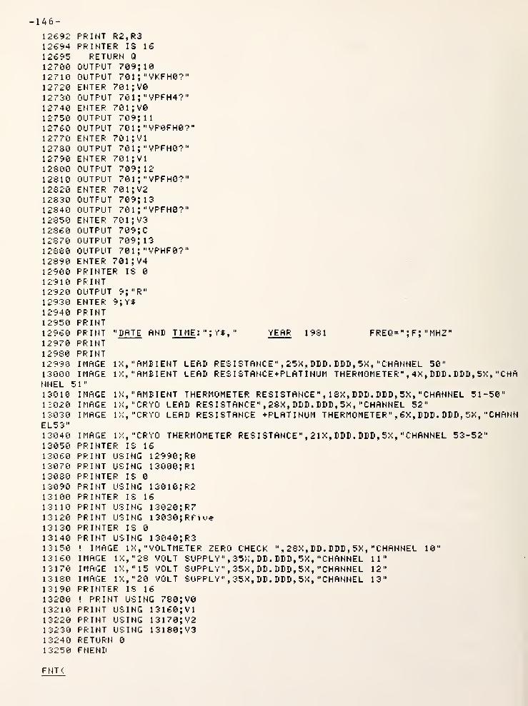
14 6 -
12692 PRINT R2,R312694 PRINTER IS 16
12695 RETURN Q
12700 OUTPUT 709; 10
12710 OUTPUT 701 ; "VKFH0?"12720 ENTER 701 ;V012730 OUTPUT 701 ; "VPFH4?"12740 ENTER ?01;V012750 OUTPUT 709; 11
12760 OUTPUT 701 ; "VP0FH0?"12770 ENTER 701; VI
1 2780 OUTPUT 701 ; "VPFH0?"12790 ENTER 701 ; VI
12800 OUTPUT 709; 1212810 OUTPUT 701 ; "VPFH0?"12820 ENTER 701 ;V212830 OUTPUT 709; 13
12840 OUTPUT 701 ;" VPFH0?
"
12850 ENTER 701 ;V312860 OUTPUT 709;
C
12870 OUTPUT 709; 13
12880 OUTPUT 701J "VPHF0?"
12890 ENTER 701JV4129O0 PRINTER IS 0
FREQ=" ;F
; "MHZ"
12910 PRINT12920 OUTPUT 9; "R"12930 ENTER 9;Y$12940 PRINT12950 PRINT12960 PRINT 11 BATE AND TIME : "; Yf ,
“ YEAR 198112970 PRINT12980 PRINT12990 IMAGE IX, "AMBIENT LEAD RESISTANCE" , 25X, DDD. DDD, 5X, "CHANNEL 50"130O0 IMAGE IX, "AMBIENT LEAD RES I ST ANCE + PLAT I HUM THERMOMETER" , 4X, DDD. DDD, 5XNNEL 51"
13010 IMAGE IX," AMBIENT THERMOMETER RESISTANCE" , 18X, DDD. DDD, 5X, "CHANNEL 51-13020 IMAGE IX, " CRYO LEAD RESISTANCE" , 28X, DDD. DDD, 5X, "CHANNEL 52"13030 IMAGE IX, "CRYO LEAD RESISTANCE +PLATINUM THERMOMETER" , 6X, DDD. DDD, 5X,
"
EL53 "
1304O IMAGE IX, "CRYO THERMOMETER RES I STANCE ", 2 1 X , DDD . DDD , 5X ," CHANNEL 53-52"13050 PRINTER IS 1613060 PRINT USING 12990JR013070 PRINT USING 13000; R113080 PRINTER IS 0
13O90 PRINT USING 13010; R213100 PRINTER IS 1613110 PRINT USING 13020; R713120 PRINT USING 13030;Rfive13130 PRINTER IS 0
13140 PRINT USING 13040; R313150 ! IMAGE 1 X ," VOLTMETER ZERO CHECK ", 28X, DD. DDD, 5X, "CHANNEL 10"
13160 IMAGE IX, "28 VOLT SUPPLY ", 35X , DD . DDD , 5X ," CHANNEL 11"
13170 IMAGE IX, "15 VOLT SUPPLY" , 35X, DD. DDD, 5X, "CHANNEL 12"
13180 IMAGE IX, "20 VOLT SUPPLY" , 35X, DD. DDD, 5X, "CHANNEL 13"
13190 PRINTER IS 1613200 ! PRINT USING 780; V013210 PRINT USING 13160; VI13220 PRINT USING 13170; V213230 PRINT USING 13180JV313240 RETURN 0
13250 FNEND
,"CHA
50"
CHAHN
FNT<

- 147 -
c 12688 12860
F * 12960
Pf * 12100
Q 1208O 12695
R0 12350 13060
R1 12400 13070
R2 * 12500 12520 12520 12692 13090
R3 * 12640 12660 12660 12692 13140
R7 12580 13110
Rf 1 ve 12620 13120
R t h r e e 12450
V0 12720 12740
VI 12770 12790 13210
V2 * 12820 13220
V3 12850 1 3230
V4 12890
Y $ 12270 12280 12930 12960

- 148 -
1 3 2 6 01 3270132801 32901 3 3 0 0
13310133201 33301 3340133501 3 3 6 0
133701 33801 3 3 9 G
1 34001 34 1 0
134 2 0
1 34 30134 4 0
134501 34601 34701 34801 34901 3 5 O 0
1351013520135301 35401 3 5 5 0
1 3 5 6 0
13570135801 3 5 9 0
1 3 6 0 0
1 36 1 0
1 36201 36301 3640136501 3 6 6 0
1 36701 36801 3 6 9 0
1370 0
1371 0
1372 0
137301 3 7 4 0
137501 3 7 6 0
1377013780137901 3 8 0 0
1381013820138301 3840138501 38601 38701 333013890
DEF FNX(Q)OPTION EHSE 1
C O M F i 1 e,F 1 ag
OMonOMOMOMOMOM
COM
Q 6 ,07, Q 8 ,Q 9 ,
R 2 ,R 3 , L ,
R,A 6 ,
R 7 ,R 8 ,
R 9 ,Z 1 , I 2 ,
N 3 , N 8 , N ,F
, F 0 ,W
8 H 0 R T F < 4 > , L < + > , M < 3 2 , 3 3 > ,H < 26, 11)
DT C 80 ]
,
Ft C 1 00 ] ,I HTEGER D < 6 , 75 > , NO , XT [ 80
]
Cf C 1 00 ] , GT C 1 00 D , RT C 1 08 ] , Ef [ 1 0 ] , HT [ 1 00 ] , 0$ C 50 3 , VT [1003ATI 100 3 ,
Z 2 ,Z 3 ,
Z 4 , Z 5 , T 1 , 81 , T4, T2, T3 , Z6 , F7 , T7 , TS , T9 , P9 , X6
,
Q 1 , Q2 , 03 , 05 ,E2
,Z : 1 , 1 88 > ,
B5,B6 , B7 ,
B8,C 1 ,
R5,P 1 ,
P2,P3
,P4
, V2P5 , F'6, F'7, PS , W 1 , N2 ,
N3,W 4 ,
W 5 , W 6 , T 5 ,T 6 ,
E 7 ,J 8 , 16,8, I 5 ,
X 3 ,P 0
,
Re al , I mag
X 7 ,X 8 , X 9
, Pout
$
I,C 2 ,
M i s rn at c h
PRINTER IS 16
PRINT "CALIBRATION FREQ" ;F
F 1 = < F - 3 0 ) 3 0
K 9 = 0
K 7 = QPRINT " 0
" ;
0
0 = 0+1PRINT "Q+l" ;Q
0 N F 1 + 1 G 0 T 0 1 3 4 60, 13470G 0 T 0 1 3 6 0 0
0 N 0 G 0 T 0 1 3 4 8 0 , 13508, 1 3 5 20, 1 3 5 4 0
Pout $="8"
GOTO 13550Pout f = "
9
"
G 0 T 0 1 3 5 5 0
P o u t f = ":
"
G 0 T 0 1355 0
Pout t=" ;
"
8 1 r o b e T = " 1"
SmoI ts$="7"Sc 1 ear*=" >
"
Zout t ="0
"
G 0 T 0 1 3 6 9 8
0 H 0 G 0 T 0 1 3 618, 1 3 6 3 0 , 1 3 6 5 8 , 1 3 6 7 0p n u t $ = " 0 "
G 0 T 0 1 3 6 9 8
Pout$=" 1
"
G 0 T 0 1 3 6 9 8
Pout $ = " 2
"
G 0 T 0 1 3 6 9 8
P o u t T = " 3 "
PRINTER IS 16
P R I H T "PR U 8 E 1 1 3 65"; P o u t $ , 8 u o 1 tsT, Sc 1 e ar
$
0 U T P U T 7 8 2;Z o u t $ ,
Z o u 1 1 , 8 m o 1 t s $
,
P o u t $!MM!)! M !
MM!!!!!!) pRUSEWRIT 250
! 0 IJ T P U T 7 8 2 ;Z o u t $ , Z o u t $ , 8 c 1 e ar T , P o u t $
! P R I N T "PR IJ SE 1 1 3 8 6 "; 8 c 1 e- ar f
WRIT 2580 = 0-1PRINTER IS 0
RETURN 0
FNENDEND
1 ALL SUBS RUN CHECK OK FINAL VS: 1-14-81! 0 = F N V = w r (. 0 >
' PRINT " T 1 , T 2 , T 3 " ; T1 ; T2; T3; " FRE0UENC V = 30MHZ
"
1 ALL SUBS RUN CHECK OK FINAL VS: 1-14-811 38 MHZ CONSTANTSi
i
I
i
OPTION BASE 1
COM File, FlagCOM Q6 , 07 , 03 , 09 , R2 , R3 , L , R , A 6 , R 7 , A 8 , A 9 , Z 1 , I 2 , N 3 , N 8 , N , F , F 0 ,
W
COM SHORT F < 4 > , L <. 8 , 20 ) , M < 32 , 33 ) , N < 26 , 11)

- 149 -
139O0 !
13910 !
13920 !
13930 !
13940 !
13950 !
13960 !
13970 !
139S0 !
13990 !
14000 !
14010 !
FNXC
F
FI
K7
K9
P o u t S
690 13
Q
13760
Sc 1 earl
S t r o b € -I
Smo 1 1 s$
COM Iif [80] ,Pit 100] , INTEGER B < 6,75), N 0 ,
X $ [ 8 0 ]
COM Cf C 1 00 3 , G* C 1 00 ] , Rt C 1 00 ] , B$ C 1 0] , H* C 1 09 ] , Q$ [ 50 3 , V$ C 1 00 3
COM fif [ 100] , Z2, Z3, Z4, Z5, T1 , SI , T4, T2, T3, Z6, F7, T7, TS, T9, P9, X6, X7, X8, X9COM Q 1 , Q 2 , Q 3 , 0 5 , E 2 , Z C 1 , 1 0 0 > , B 5 , E 6 , B 7 , E 8 , C 1 , R 5 , P 1 , P 2 , P 3 , P 4 , V 2 ,
P o u 1
1
COM P 5 , P 6 , P 7 , P 8 , U 1 , N 2 , W 3 , H 4 , W 5 , W 6 , T 5 , T 6 , E 7 , J 8 , I 6 , S , 1 5 , X 3 , P 0 ,I
COM Real , I magReal =R=52I rn ag — 1
Tl=l 1000T 2 = 2 9 6 . 00T 3 = 7 6 . 00PRINT " T 1 , T 2 , T 3 " ; T1 ; T2; T3; " FREQUENC V = 30MHZ
"
* 13380 13390
13390 13450
1 34 1 0
134O0
* 13480 135O0 13520 13540 13610 13630 13650 13670 13
13260 13410 13420 13430 13430 13440 13470 13600 13760
13570 13690
13550
13560 13690 13700
Z o u t $ 13580 1 3 7 0 0 1 3700
-ISO-
140201403014040140501406014070140301 4 0 9 0
141001411014120141301414014 150141601417014130141901420014210142201 423014240142501 4260
DEF FNVswr < Q ) ! 30 MHZ VS 3-2-81 GJCOPTION BfiSE 1
COM File, FlagCOM Q6,Q7,Q8,Q9,R2,R3,L,R,fi6,fl7,fi8,fl9,21,I2,N3,N8,N,F,F0,WCOM SHORT F<4>
, L<8, 20) ,MC32, 33) , N<26, 1 1 >
COM D* C SO ], Ft [ 100] , INTEGER B<6, 75) , N0, X$C803COM C$C 100 3 , G$C 100 3 , RtC 1003 , B$C 103 , H$C 1003 , Q$C 50] , V$ C 1 00 3
COM ft $ [ 1 0 0 3 , 22, Z3, Z4, Z5, T1, SI ,
T4, T2, T3, 26, F7, T7, TS, T9, P9, X6, X7, X8, X9COM Q 1 , Q2 , Q3 , 05 ,
E2 , Z <1 , 1 00 ) , B5 , B6 , B7 , BS , C 1 , R5 , P 1 , P2 , P3 , P4 , V2 , Pout $
COM P5,P6,F'7,P8,W1,W2,W3,W4,W5,W6,T5,T6,E7,J8, 16, S, 15, X3, P0, I , C2, Mi smatc
h
COM Real , I magDIM B i < 60 ) ,
I < 60 ) , M i < 60 ) , N i < 60 ) , E i < 60 ) , C i < 60 ) , 2 i < 60 ) , G i $ C 1 00
3
!{MM
j !!!!!!!!!!! j !!!!!!!!!!!!!! FNGPRINT T 1 , T2 , T3 ;
" FREG =30MHZ
"
X = R e a 1
V = I m agQ z e r o = < X + 5 0 > 2 + Y A2Clone =Qzero*QzeroG 1 = < X '•2-2500 + Y •2 ) /QzeroG2= 1 00* Y ' Q z e r o
Qthr =100*fiBS< < X +50
)
A2-YA2) * .
5
G3= C Qt hr +RBS <. 200* Y* < X +50 ) * 1 > > .''Gone
Qfour = 200*flBS < Y * < X +50 ) ) * .
5
Qe i ght = < X +50 > '-2
Q s e u e n = Y - 2
14270 Qf i ve= 1 00*fiBS < Qeight -Qseven ) * 1
14280 G4= <Qf our+Qf i ye)/Qone14290 ! GOTO 730914300 PRINT M Y";Y,"R";X14310 PRINT14320 PRINT14330 PRINT " G" 1 ' G" “
;" BG''";"
DC''" "
14340 PRINT G1,G2,G3,G414350 PRINT14360 PRINT14370 G5= < < X-50 ) A 2 + Y-'-2 ) /Qzero14330 Qf i ue =200 * <
X
a2-2500-Y a 2 ) * .
5
1 4390 Qf i ve=fl£S < Qf i ue
>
1 4400 G6= ( Qf i e + 4 0 0 * ft B S < X* Y > * 1 ) Clone
14410 PRINT " G ft M M ft SQ"," D GftMMfi SQ"14420 PRINT G5,G61443G PRINT14440 Z o n e = X / 5 0
14450 Ztwo=Y/5014460 Z z e r o = S Q R < < X A 2 + Y 2 ) / 2 5 0 0 )
14470 G 7 = < Z z e r o '• 2 - 1 )/(Zzero
2
+ 1 + 2 * Z o n e
)
1 4480 G 8 = 2 * 2 1 wo/<2zero A2+ 1 +2*Z1
>
14490 G9=SQR<G7*G7+G8*G8>14500 Zn i ne= < GS G9
>
A 214510 ft 1 = ft T N < G 8 ' G
9
/ S Q R < 1 -Zn i ne + . 0000000 1 ) )
14520 PRINT "GftMMfi R "J
" GftMMfi I";" GftMMfi MfiG" J
"
ftNGLE
"
14530 PRINT G7,G8,G9,ftl14540 BISP T 1 , T 2 , T
3
14550 T f i oe = T 1 *T314560 T e i x = T 1 *T214570 T e euen =T3*T214580 T e
ight =T3-T2
14590 T z e r o = T 2 - T
3
14600 Tni ne=T 1-T214610 Cone =88.
1
14620 ' CHECK CONSTfiNTS USED IN THIS ROUTINE14630 Ctwo=80.2

14640 C t h r e e = 9 . 8
14 650 C f o ur = 5 .
8
14660 H=- . 00514670 H 1 =0146S0 H2=. 00514690 Ri =. 16214700 R o n e = . 18614710 P o n e = G 1
14720 P t- w o = G 2
14730 P t. h r e e = G 3
14 740 Pfour=G414750 Y= 1
14760 F9=014770 GOTO 1621014780 ! ! M !
1 i
! M !!!!!!!!!!!!! FND14 790 I n d ex=
2
1430O T= 1
14810 FOP L = O TO 3
14820 GOTO 1486014830 12=1 1=17=1 8=Pt wo14840 B3=B4=B5=B6=Po n
e
14850 GOTO 1490014 860 I l = I2=Ptwo + Pfour14870 I7=IS=Pt w o - P f o u r
14880 B 3 = B 4 = P o n *• + P t h r t <=•
1 4 89 0 B 5 = B 6 = P o n t - P t- h r t e
1 4900 B 1 = B7 = Pone + L*F't hree-''3
14910 B 2 = B 8 = P o n e - L * P t h r e e /
3
14920 1 3 = 1 5 = P t- w o + L * P t o u r 3
14 930 1 4 = 1 6 = P t wo - L * P f o u r 3
14940 ! PRINT L,I514950 Bi CL+l )=B114960 IF L=0 THEN 1498014 970 B l C L + 4 J = B 2
14980 B i < L + 8 > = B
3
14990 IF L=0 THEN 1501015000 Bi CL+l 1 >=B415010 B i <: L + 1 5 > = B 5
15020 IF L=0 THEN 158481503 0 B i CL+l 8 :> = B 6
15040 Bi C L + 2 2 ) = B 7
15058 IF L=0 THEN 1507015060 B i C
L
+ 25 > =B815070 I CL+l > = II
15880 IF L=0 THEN 1518815090 I CL + 4> = I215100 I C L + 8 > = I 3
15118 IF L=8 THEN 1513015120 ICL+m = I415138 ICL+15>=I515140 IF L=8 THEN 1516815150 ICL+18>=I615160 I C L+22 > = I 7
15170 IF L=8 THEN 1519015180 I C L + 25 > = 1815190 NEXT L
15200 IF Y =51 THEN 16578 !!!!!!!!!15210 IF V=52 THEN 16828 !!!!!!!!!!15220 IF Y = 3 THEN 16858 !!!!!!!!!!15238 IF Y = 8 THEN 1785015240 !
(MM!!!!!! HM! M !!!!!!!!!!!!! F N M
15258 FOR 0=1 TO 2815268 U 2 e r
o
=£ Q R C B i C Q > * B i < 0 ) + 1 C 0 > * I < Q > >
15270 W z e r o = 1 - H z e r o * U z e r
o
15280 Wone=l-H2*H2
1
6
;1
7
I
! ! ! RETURN FNC1! ! ! RETURN TO FNC2! ! ! RETURN TO FNH Y

-152-
1529 0 W t. w o = < 1 - H * D i ( G! > + H 1 * I ( Q > >A 2
1 5 3 0 0 N t h r e-e=<H*I<Q>+Hl*Di ( Q > > 2
1 5 3 1 O W f o u r = N z € r o * N o n e x ( N t w o + N t h r e e i
1532 0 M i ( Q > = W f o u r
15330 NEXT Q
15340 PRINT15350 ! !!!!!! t !!!!!!!!!! 1 !!!! j
i !!!!!!!! § !!!!!!!!!!! F H M
15360 FOR Q= 1 TO 281537 0 V 1 = <! R i + B i <Q > >
••••• 2 + (. R o ri •=• + I < Q > )'• 2
15380 V 2 = <. 1 -H*D l < Q > +H 1 * I < Q > ) A2+ C H * I ( Q > +H 1 *B i < Q ) >-'"2
1539 0 N i < Q = C o n e + C t w o * < V 1 / V 2 >
1540O NEXT Q
15410 GOTO 1628015420 !
i mmmjmm m MM!!!!!!! mm M MM! mi M
jm p n i
j
15430 IF F 9 = 0 THEN 1546015440 M 1 = M 2 = M 3 = M i ( 1
>
15450 N i1 = N i 2 = N i 3
15460 K =
1
154 70 FOR 0 = 1 TO 2
8
15480 IF F9= 1 THEN 1557015490 IF K = 1 THEN 1552015500 IF K = 2 THEN 1560015510 IF K = 3 THEN 1565015520 N i 1 = N i < Q >
15530 N i 2 = N i 3 = Ni < 1 >
15540 M 1 = M i < Q
>
15550 M 2 = H 3 = H i < 1 )
15560 GOTO 1569015570 M 1 = M 2 = M 3 = M i 1 >
1 5 5 8 0 Hi 1 = N i 2 = N i 3 = N l < Q >
1559 0 G 0 TO 1569
0
156 O 0 H l 2 = N i < Q
15610 Ni 1 = N i 3 = N i < 1
>
15620 M 2 = M i < Q
>
15630 M 1 = M 3 = M i < 1 >
1564 0 G 0 T 0 1 5 6 9 0
15650 M 3 = M i < Q >
15660 M 1 = M 2 = M i < 1
>
1 5 6 7 0 N i 3 = N i < Q >
1 5 6 8 0 Hi 1 = N i 2 = N i>'
1 >
1 5 6 9 0 E O — T t l u € + (. M 3 - M 1 .j + T $ i x * M 1 — M2! .> + T s t €• n * ( M 2 — M 3 )
15780 Z 9 = T n } n e * < N i 3 - N i 2 > + T z e- r o * ( Hi 1 - N l 2
>
15710 E l < Q > = :! E 0 + Z 9 > x T € i g h t
15720 NEXT Q
15730 E 9 = 0
15740 E = E i ( 1
)
15750 FOR Q= 1 TO 2815760 E 1 = E i <
Q
>
15770 IF RB8CE-E1 XE9 THEN 1579015780 E 9 = fl B S C E - E 1
>
15790 NEXT Q
15800 IF K = 1 THEN 1583015810 IF K = 2 THEN 1587015820 IF K=3 THEN 159101 5 8 3 0 S 1 = E 9
15840 E 1 = E i < 1
>
15850 K = K +
1
15860 GOTO 1547015870 S 2 = E
9
15880 E 1 =E < 1
>
15890 K = K +
1
15900 GOTO 1547015910 S3=E915920 E1=E<1>15930 K = K +
1

- 153 -
15940159501596015970159801599016000160101 60201 603016040160501 6060160701608016090161001611016120161301614016150161601617016180161901 620016210162201 6 2 3 O
162401 62501626016270162801 62901 63001631016320163301 6340163501 6 3 6 0
16370163801 639016400164101642016430164401645016460164701648016490165001651016520165301654016550165601657016580
IF V = 5 THEN 16440IF Y = 5 1 THEN 16710IF Y=52 THEN 16960IF Y=8 THEN 17110GOTO 16300
I ! M ! M !!!!!!!!!!!! ;MM
; !!!! j !;; I!M
j ; j j ; !j Ij
I
p
NHP c n e = H
P t w c = H 1
P t h r e e = . 0 0 5
Pfour = . 01
IF Y = 3 THEN GOTO 14780 !!!!!!!!!!!!! ! Q =FND(Q>FOR 0=1 TO 28Wzero =SQR < G 1 *G 1 +G2*G2
)
Wzero= 1 -Wze ro*WzeroT e rn p = S Q R < D i C 0 ) * D i <Q) + I(Q)*I<Q)>Uone=l-Temp*Te m pW t w o = < 1 — D i <Q)*G1 + I (Q>*G2>'"-2U t h r e e = < D i <Q>*G2+I <Q>*G1
)
A 2
Wfour=Wzero*Wone/ < Wt wo+Wt hree)Mi <Q)=WfourV 1 = < R i + G1 > ' 2 + < R o n e + G 2 > ^ 2
V2=<1-H*G1+H1*G2> A2+<H*G2+H1*G1) A 2
Ni < Q ) = C o n e + C t w o * <! V 1 / V 2
)
NEXT Q
IF Y = 3 THEN 16410 ! ! RETURN FROM FNH Y = 3
Y = 0
GOTO 14160! ! ! RETURN #1 FROM FNGP o n € = G
1
P t wo = G
2
P t h r t € = G 3
P f o u r = G 4
Y= 1
GOTO 14780 ! Q=FND < 1 > + FNM < 1 > +FNN C 1
>
GOTO 15420Y = 3
Q o n €' = 3
1
Q t w o = S 2
Q t. h r € t = i
! SET FOR FNH HEREP o n € = H
P t w o = H
1
P t h r e € = . 005P f' o u r = . 01
GOTO 15990! Y = 4
Y = 4
Y = 5
GOTO 15420Qf our =S
1
Qf i '>
e
= S
2
Q « i x = S 3
I ride x = 4
F9= 1
IF I ridex >4 THEN 16750! (!!!!!!!!!!!!!!!!!!!!!!!!
! Q=FN0CQ>! RETURN FROM FNO
! Q =FNH < 1
>
'.RETURN FROM FNH! RETURN FROM FNH
! Q=FN0< 1
>
! ON INDEX GO TO FNC< INDEX)
! ! ! Q = F N C 1
Pone = Ct woP t w o = 0
Pt hre e = 7 . 28P t o u r = 0
Y = 5 1
GOTO 14780 IFNDC1.)
FOR Q= 1 TO 28Wzero=SQRtGl*Gl+G2*G2)

- 154 -
1 6 5 90 Uze ro= 1 -Wz € r o ' 2
16660 Wone=l-H2*H216610 W t w o = ( 1-H*G1+H*G2 >
A 2
1 6 6 2 0 M t h r ee=CH*G2 + Hl*Gl > 2
166 3 0 kl f o u r = W z <=• r o * W o n e- •/
<. W t w o + W t h r * ۥ >
1 6640 M i < Q >=Wfour1665 0 V 1 = ( R i + G 1 ) '' 2 + ( R o n e- + G 2 )
A 2
16660 V 2 = ( 1 - H * G 1 + H * G 2 ) 2 + ( H * G 2 + H 1 * G 1 .>A 2
16670 V 3 = V 1 V
2
1 6 6 8 0 N i < Q > = C o n e + D i < Q > * V 3
1 6 6 9 O N E X T Q
16700 GOTO 15420 ! Q= F H 0 C Q >
16710 Y=6 ! RETURN FNO167k' U Q s t € fi - S 1
167 3 0 Q e i g h t = S
2
1674 0 Q n i n e = S 3
16750 ! M !!!!!!!!!! M M!!!!!!!!!!!! ! F N C 2
1 6 7 6 O V = 5216 770 P o n t = . 3 2 8
2
1673 0 P t w o = . 026216790 Pthree=. 0311 6 8 0 0 P f o u r = . 0 6 5
16810 GOTO 14780 ! G = F N D
1
16820 FOR Q= 1 TO 28 1 RETURN FHD1 6 8 3 0 V 1 = C D i < Q > + G 1 > 2+< I < Q >+G2 )
2
1 6840 V2 = ( 1 - H * G 1 + H 1 *G2 > "•2+ < H*G2+H 1 *G 1 >•"2
1 6 8 5 O H i (. Q ) = C o n e + C t w o * ( V 1 / V 2 )
16860 Wze r o = 1 - W z e r o
2
16870 Wone=l-H2*H21 6 8 8 0 W t 1,1 o = C 1 - H * G 1 + H 1 * G 2 > 2
1 6890 Wt hr e e= < H*G2 + H 1 *G 1 > "-2
1 6 9 0 0 N f o u r = N z e r o * N o n e / < N 1 1...1 o + U t h r e e >
16910 Mi <Q>=W four-
16920 NEXT Q
16930 F9=
1
16940 Y = 5
2
16950 GOTO 15420 ! Q = F H
0
16960 U1 =31 ! RETURN FNO16970 U 2 = S
2
1 6 9 8 0 U 3 = S 3
1 6 9 9 0 Y = 8
1 7 0 0 0 P o ne = H
17010 P t w
o
= H
1
1702 0 P t h r e t = . 0 0
5
17030 Pfour =.0117040 GOTO 14780 ! G=FND1705 0 V 1 = < R i + G 1 ) 2 + < R o n e + G 2 ) 2 ! R E T U R N F N D
17060 FOR 0=1 TO 231707 0 V 2 = C 1 - D 1 < Q > * G 1 + I < Q > * G 2 >
' 2 + D i < Q * G 2 + < I < G > * G 1 ) 2
1708 0 N i < Q "> = C o n e + C t w o * < V 1•••' V 2 >
17090 F9=
1
17100 GOTO 15420 ! Q = F N
0
17110 U 4 = S 1 ! RETURN FNO17120 U 5 = S
2
17130 U 6 = 8
3
17140 PRINTER IS 0
DSN 1 , DSN2 , DSN3 :%U1, U2
,U3
US 1 1 N 1 ,DS 1 1 N2
,US 1 1 N 3 : "
,U4
,U5
,IJ6
G o n t , G 1 1.1.1 o,G t h r t e
: “,Q f o u r
,Q f i u e
,G s i x
2 N 3 : ",G s e € n , Q t i 9 h t
,G n i n e
17210 PRINT PHGE17 220 Mi £ rri a t c h — S G R (. G o n e 2 + G t w o A £17221 FIXED 2
+ Q t h r e e " 2 + G f o u r
2
+ Q f i u e
2
+ Q s i x
2
+ 0 s «•<.>
e
n + Ul+U4)

- 155 -
17236 PRINT17240 RETURN17250 FNEND
"SUMMATIONQ
U F M I b M A T C H E R R u R S = <! R S S ) "; M i s- rri at c h
FNVswr
<
A 1 14516 14530
C f o u r 14656
Ci < 14136
Cone 14610 15396 1 6 1 6 0 i 6 6 8 0 1685 0 1768 0
Ct hree 14646
C* wo 14630 1 5390 16160 16516 16850 17080
D
1
149O0 14950
D2 14910 14970
D3 1484 0 1488 0 1 4 9 8 0
D4 14840 14880 1 5 0 0 0
ns 14840 14890 15010
D6 14840 1 4890 1 5030
D7 14900 1 5040
1)8 1 49 1 0 15060
Di <
15260 15266
830 17670
1 4 1 3015290 15
1
17070
149503005370 1
14970 14 9 8 0 1 5 0 6 0 1501 0 1 5 0 3 0 1564 6 1506 6
5386 15386 16086 16686 16106 16116 16686 16
E 15746 15776 15786
E < 15886 15926
E6 15696 15710
El 1 5766 15776 15786 15840 1 5886 15926
E9 15730 15776 1 5786 15836 1 5876 15916
Ei < 14136 15716 15746 15766 15840
F9 14766 15430 15486 1 6486 1 6936 1 7696
G
1
14260 1 4 3 4 0 14716 1 6 0 6 6 1666 0 16160 16116 16146 16150
16150 16226 16586 165 8616616 1 6626 1 6656 1666 6 16666 16830 16S46 16i40 16
880 18890 17050 1707017070
G2 14210 14340 14720 16060 16060 16100 16110 16146 16156
16150 16230 16580 1658016610 16620 16650 16660 16660 16830 1
6
8 4 6 1
6
8 4 6 1
6
880 16890 17050 1707017670

- 156 -
G3 14230 14340 14730 16240
G4 14280 14340 14740 16250
G5 14370 14420
G6 14480 14420
G? 14470 14490 14490 14530
G8 14480 14490 14490 14500 14510 14530
G9 14490 14500 14510 14530
Gi $ 14130
H 14660 15290 1 5300 15380 15380 16000 16150 16150 1635016610 16610 16620 16660
16660 16660 16840 16840 16880 16890 17000
HI 14670 15290 15300 15380 15380 16010 16150 16150 1636016620 16660 16840 16840
16880 16890 17010
H2 14680 15280 15280 1660O 1 6600 16870 16870
I < 14130 15070 15090 15100 15120 15130 15150 15160 1518015260 15260 15290 15300
15370 15380 15380 16080 16080 16100 16110 16830 17070 17070
I 1 14830 14860 15070
12 * 14830 14860 15090
13 14920 15100
14 14930 15120
15 * 14920 15130
16 * 14930 15150
17 14830 14870 15160
18 14830 14870 15180
I mag * 14170
Index 14790 16470 16490
K. 15460 15490 15500 15510 15800 15810 15820 15850 1585015890 15890 15930 15930
L * 14810 14900 14910 14920 14930 14950 14960 14970 14980 14990 15000 15010
15020 15030 15046 15050 15060 15070 15080 1 5090 15100 15110 15120 15130
15140 15150 15160 15170 15180 15190
Ml 15440 15540 15570 15630 15660 15690 15690
M2 15440 15550 15570 15620 15660 15690 15690
M3 15440 15550 15570 15630 15650 15690 15690

-15 7-
M i < 14130 15320 15440 15540 15550 15570 15620 15630 1565815660 16130 16640 16910
M 1 srn at c h * 17220 17230
Ni ( 14130 15390 15520 15530 15580 1 5600 15610 15670 1568016160 1 6680 16850 17080
Ni 1 15450 15520 15580 15610 15680 15700
Ni 2 15450 15530 1 5 5 8 0 1 5600 15680 15700 15700
Ni 3 15450 15530 15580 15610 15670 15700
Pfour 14740 14860 1487 0 14920 14930 1 6 0 3 0 16250 16380 165401 6800 17030
Pone 14710 14840 14880 14890 14900 14910 16000 16220 1635016510 16770 1 7000
Pt hree 14730 14880 14890 14900 14910 1 6020 16240 16370 1653016790 17020
P t w o 14720 14830 1 4 8 6 0 14870 14920 1 4930 16010 1623 0 1 6 3 6 0
16520 1 6780 17010
Q 14020 15250 1 5260 15260 15260 1 5260 1529 0 152 9 0 1 5 3 0 0
153O0 15320 15330 1536 0
15370 15370 15 3 3 0 15380 15380 15 3 8 0 15390 154 0 0 1
5
470 15520 1 5540 1558
0
156 0 0 15620 15650 15670 15710 15 720 15750 15760 15
790 16050 16080 160801 6080 1 6 0 80 16 1 00 1 6 1 00 161 10 16110 16130 1 6 1 6 0 16
170 16 570 1 6 6 4 0 1 6 6 8 0
1 6680 16690 16 8 2 0 16830 16830 16 850 16910 16920 17
060 17 070 1 7070 1707017070 17080 17 240
Qeight 14250 14270 1 6730 17170
Q f i o e 14270 14280 14380 14390 14390 14400 16450 17160 17220
Qf our 14240 14280 1 6440 17160 17220
G n i n e 16740 17170
Gone 14190 14230 14280 14 4 00 16310 17150 17220
Q s e u e n 14260 14270 16720 1 7 1 70 17220
Gs i x 16460 17160 17220
Qt hr 14220 14230
G t h r e e 16330 17150 17220
G t. w o 16320 17150 1 7220
Gzero 14180 14190 14190 1 4200 14210 14370
Real * 14160
Ri 14690 15370 16140 16650 17050
Rone 14700 15370 1 6 1 40 1 6 6 5 0 17050
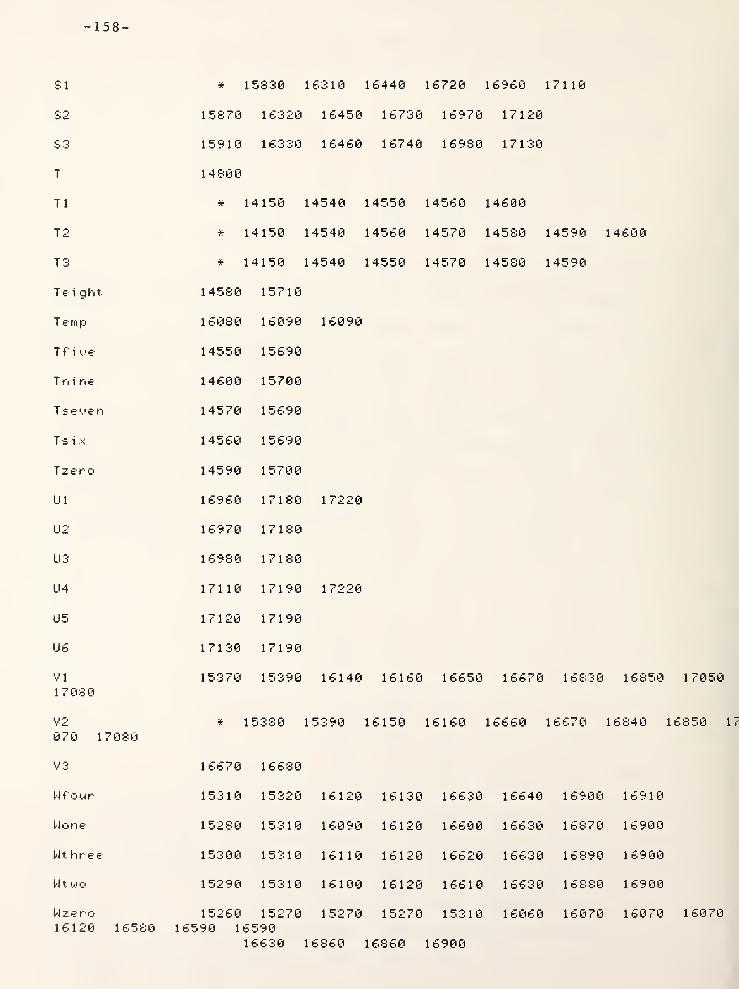
- 158 -
SI * 15830 16310 16440 16720 16960 17110
S2 15870 16320 16450 16730 16970 17120
C; 15910 16330 16460 16740 16980 17130
T 14800
T 1 * 14150 14540 14550 14560 14600
T 2 * 14150 14540 14560 14570 14580 14590 14600
T 3 * 14150 14540 14550 14570 14580 14590
T e i q h t 14580 15710
T e rn p 16080 16090 16090
T f i ye 14550 15690
T n i n € 14600 15700
T £ €' e n 14570 15690
Til x 14560 1 5690
T zero 14590 15700
U1 1 6960 17180 17220
U2 1 6970 17180
U3 16980 17180
LI 4 17110 17190 17220
U5 17120 17190
U6 17130 1 7 1 90
VI1 7 0 8 0
15370 15390 16140 16160 16650 16670 16830 16850 17050
i i oV £.
070 17 0 8
0
* 15380 15390 16150 16160 1 6 6 6 0 1 6 6 7 0 16840 16850 1
V3 16670 1 6680
Wf our 15310 15320 16120 16130 16630 16640 16900 16910
W o ri e 15280 15310 16090 16120 16600 16630 16870 16900
W t h r e e 1 5300 15310 16110 16120 16620 1 6 6 3 0 16890 169 0 0
W t w o 1 5290 15310 16100 16120 16610 16630 16880 1 6900
W 2 e r o
16120 1658015260 15270 15270
16590 1659016630 1 6 8 6 0
15270 15310
16860 16900
16060 16070 16070 16070
16860 16860 1690O

159 -
14460 14750 15200 15210 15220 15230 15940 15950 15
960 15970 16040 1618016190 16260 16280 163O0 16410 16420 16550 16710 16
760 16940 16990
21 * 1 4480
29 15700 15710
2 i < 14130
2n i ne 14500 14510
2one 14440 14470
2t wo 14450 14480
2zero 14460 14470 14470 14480

tm172701728017290173001731017 201733017340173501736017370173801739017400174101742017430174401744217443174441744617460174701 748017490175001751017520
DEF FNData(Q)OPTION BASE 1
COM F i 1 e , F 1 agCOM 06, 07, Q8, 09, R2, R3,L,R, A6, A7, Fl8, fl9, Z1 , 12, N3, N8, N, F, F6, M
COM SHORT F<4) , L<8, 20) , M02, 33 > , N<26, 1 1
)
COM D$ [ 80 3,P*[ 100], INTEGER D < 6 , 75 > , N0 , X* C 80
3
COM C$ C 1 00 ] , C 1 00 D , Rt C 1 00 3 , B$ C 1 0 ] , H$ C 1 00 ] , C 50 ] , V$ C 1 80
]
COM A* [ 100 3 , Z2, 23, 24, Z5, T1, SI , T4 ,
T2,T3 , Z6 ,
F7,T7
,T8
,T9 , F*9 , X6 ,
X7, X8 ,
X9COM 0 1 , 02 , 03 , 05 , E2 , Z < 1 , 1 00 ) , B5 , B6 , B7 , B8 , C 1 , R5 , F 1 , P2 , P3 , P4 , V2 , Pout *
COM P5,P6 ,
P7,P8
,W 1 ,
W2 ,W3
,W4
, M5 , W6 ,T5
,T6
, E7 , J8 ,1 6 ,
S, 1 5 ,
X3, F'0, I ,
Mi srr.at c
h
COM Real ,Irnag
MASS STORAGE IS " :T14"INPUT "TAPE # , F I LE NAME " ,T,0$ASSIGN #1 TO 0$READ #1 ; H$C 1 , 1803, Z<*>, C*C 1 , 1003 , G$C 1 , 1003
!, R*C 1 , 1003
ASSIGN #1 TO *
REM PRELIMINARY RESULTSA$=" "
PRINTER IS 0
! PRINT PAGEFIXED 2
PRINT "TOTAL MISMATCH ERROR I S Z <1 , 26 >;
" DEGREES KELVIN"PRINTOUTPUT 9;"R"ENTER 9 ; F'$
PRINT TAB < 20) , "DATE: " ; P* C 1 , 23 ;; Pf C4, 53
; "-1981" ;" TIME: P$C7, 143
PRINTPRINT TAB(6>,A$PRINT T A B ( 6 )
, "TAPE # :
" ; T,
" F I LE :
" ; Of ; TAB <50 > ; R* El, 193FOR 1=1 TO 11
17530 PRINT17540 NEXT I
17550 PRINT TAB < 23 31
,"MEASUREMENT RECAP"
17560 PRINT TABOO), "AND"17570 PRINT TAB<22) , "PRELIMINARY RESULTS"17580 FOR 1=1 TO 7
17590 PRINT17600 NEXT I
17610 Z < 1 , 34 ) =3017620 PRINT T A B < 6 )
," FREQUENCY* TABU 6 ); Z U , 34 >
; "MHZ"17630 PRINT TAB < 6)
, "SOURCE IMPEDANCE" ; TAB < 23) , H*C 1 1 , 203 ; TAB 08) , "LEVEL SETTING 0
F A2=" ; Z(1 , 51 )
17640 PRINT T A B 6 > ,A $
17650 PRINT17660 PRINT17670 PRINT TAB<10> , "TA" ; TAB < 20) ,
" R OHMS " ; TAB < 34 ),
" TS " ; TAB C 44 ),
" R OHMS"17680 PRINT TAB < 6 ) ,
" "
17690 FIXED 2
17700 PRINT TAB < 8 ) , Z< 1 ,1 ) ; TAB < 20)
,
Z< 1 , 59) ; TAB (32) , Z< 1 , 2) J TAB < 44) , Z< 1 , 60 >;
"
T 50 MEASUREMENTS)"17710 PRINT T AB < 8 ) , Z <1 , 7 ) ; T AB < 20 ) , Z < 1 , 59 ) ; T AB 02 ) , Z <1 , 8 ) ; TAB < 44 ) , Z < 1 , 60 ) ;
"
D 50 MEASUREMENTS)"17720 PRINT TAB<6),A$17730 PRINT TAB< 1 1 )
, "TX" ; TAB <21 ), "SX" ; TAB < 34) , "TE"
17740 PRINT TAB < 6 ) ,
" "
17750 PRINT T AB < 8 ) , Z < 1 , 3 ) ; T AB < 20 ) , Z < 1 , 4 ) ; T AB 02 ) , Z <1 , 5 ) ;
"
CIS
<2N
17760 PRINT TAB < 8 ) , Z < 1 , 9 ) ; TAB < 20 ) , Z C 1 , 1 0 ) ; TAB 02 ) , Z < 1 , 11);"
NTS) "
17770 PRINT'^780 PRINT TAB < 6 ) , Af
a ST 50 MEASUREMENT
< 2ND 50 MEASUREME
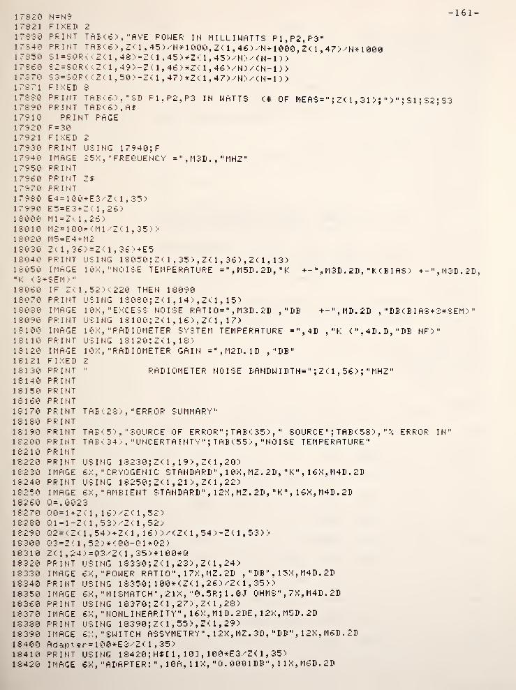
- 161 -17820 N = N917821 FIXED 2
17830 PRINT TAB(6),"AVE POWER IN MILLIWATTS P1,P2,P3"17840 PRINT TRE < 6 ) ,
Z < 1,45) - 'N* 10G0, ZC 1 , 46) N* 1 000 ,Z ( 1 , 47 ) ,'N* 1 000
17850 S1=SQR< <Z< 1 , 48)-Z<l ,45)*Z< 1 , 45) /N ) < N- 1 ) )
1 7860 S 2 = S Q R ( <Z< 1 , 49>-Z( 1 , 46)*Z< 1 , 46) / N
)
/ <N - 1 >
)
17870 S3-3QP C < Z ( 1 , 50 ) -Z < 1 , 47 ) *Z < 1 , 47 ) ."N ) / ( H- 1 ) )
17871 FIXED S
17380 PRINT TABC6),"SD F1,P2,P3 IN WRTTS ( # OF MEfiS* " ; Z < 1 , 3 1 )J
">" ; S 1 ; 82 : S3
17890 PRINT TABC6),A*17910 PRINT PRGE17920 F=3017921 FIXED 2
17930 PRINT USING 17940;
F
17940 IMRGE 25X ," FREQUENCY =
" , M3D .
," MHZ
"
17950 PRINT17960 PRINT Z$17970 PRINT17980 E4=100*E3 Z ( 1 , 35)17990 E5=E3+Z< 1 , 26)18000 M 1 = Z ( 1 , 2 6 )
18010 M2= 1 00* ( M 1 s' 2 (1,35 ) )
1802O M5=E4+M218830 Z < 1 , 36 ) =Z ( 1 , 36 ) +E518040 PRINT USING 1 8050 ; Z ( 1 , 35 ) , Z <1 , 36 ) , Z < 1 , 1 3
)
18050 IMRGE 10X, "NOISE TEMPERATURE =" , M5D . 2D , " K + -
" , M 3 D . 2 D,
" K (BIAS) +-",M3D.2D," K ( 3 * S E M )
"
18060 IF Z( 1,52) <220 THEN 1809018070 PRINT USING 1 8080 ; Z < 1 , 1 4 ) , Z ( 1 , 1 5
)
18080 IMRGE 10X, "EXCESS NOISE RATIO* ", M3D. 2D ,"DB +-",MD.2D , " DEC B I RS +3*SEM) "
18O90 PRINT USING 1 8 1 00 ; Z ( 1 ,1 6 ) , Z ( 1 ,
1 7 )
18100 IMRGE 10X, "RADIOMETER SYSTEM TEMPERATURE =",4D , "K <",4D.D,"DB NF)“18110 PRINT USING 1 8 1 20 ; Z ( 1 ,
1 8
)
18120 IMRGE 10X, "RADIOMETER GRIN =" ,M2D.1D ,"DE"18121 FIXED 2
18130 PRINT " RADIOMETER NOISE BRNDU I DTH= " ; Z ( 1 , 56 );
" MHZ
"
18140 PRINT18150 PRINT18160 PRINT18170 PRINT TAE ( 28 )," ERROR SUMMARY
"
18180 PRINT18190 PRINT TAB (5), "SOURCE OF ERROR TAB ( 35 ), " SOURCE TAB < 58 ),"
X
ERROR IN"1 8200 PR I NT TAB ( 34 ) , " UNCERTR I NTY " ; TAB < 55 >
," NO I SE TEMPERATURE
"
18210 PRINT18220 PRINT USING 1 3230 ; Z ( 1 , 1 9 ) , Z ( 1 , 20
)
18230 I MAGE 6X,
" CRYOGEN I C STANDARD " , 1 0X , MZ . 2D ,"K
" , 1 6X , M 4 D . 2D18240 PRINT USING 1 8250 ; Z < 1 , 2 1 > , Z < 1 , 22
)
18250 IMAGE 6X, "AMBIENT STANDARD ", 1 2X , MZ . 2D ,"K
" , 1 6X , M4D . 2D18260 Q= . 002318270 Q0= 1 +Z ( 1 , 1 6
)
/Z ( 1 , 52
)
18280 Q 1 = 1 -Z < 1 , 53 ) /Z < 1 , 52
)
1 8290 Q2= ( Z( 1 , 54 ) + Z ( 1 ,16 ) ) / < Z < 1 , 54 ) -Z ( 1 , 53 )
)
1 8300 Q 3 = Z ( 1 , 5 2 ) * ( Q 0 - Q 1 * Q 2
)
18310 Z ( 1 , 24 ) =Q3.'Z < 1 , 35 ) * 1 00*018320 PRINT USING 1 8330 ; Z ( 1 , 23 ) , Z ( 1 , 24
)
1 8330 IMAGE 6X ," POWER RAT I 0 "
,1 7X , MZ . 2D , " D B " ,
1 5 X , M 4 D . 2 D
18340 PRINT lJ S I NG 18350 ;1 00* ( Z ( 1 , 26 ) - Z < 1 , 35 )
)
1 8350 IMAGE 6X ," M I SMATCH " , 2 1 X
," 0 . 5R ;
1 . 0J OHMS " , 7X , M4D . 2D18360 PRINT USING 1 8370 ; Z < 1 , 27 ) , Z ( 1 , 28
)
1 8370 IMAGE 6X ," NOHL I NEAR I TY " ,
1 6X , M 1 D . 2DE,
1 2 X , M 5 D . 2 D
18380 PRINT USING 1 8390 ; Z ( 1 , 55 > , Z <1 , 29
)
18390 IMAGE 6X, "SWITCH ASSYMETRY", 12X,MZ.3D, "DB", 12X.M6D.2D18400 Adapt er=100*E3/Z( 1,35)18410 PRINT USING 1 8420 ;
H$ [ 1 , 1 0 ] ,1 00*E3-'Z < 1 , 35
)
18420 IMAGE 6X, "ADAPTER: ",10ft, 1 IX, "0. 0001 DB" , 1 IX, M6D. 2D

- 162 -
1 843018440184501846018470184801849018500185101852018530185401S55018560185701858018590186001861018620186301864018650186601867018680186901870018710187201873018740187501876018770
PRINT TAB<6),A#Su=100*Z<l,26>/Z<l,35>Suu= 1 00*E3^Z <
1
f 35)Surnm=Z < 1 , 20>+Z< 1 , 22)+Z< 1 , 24)+Su+Z< 1 , 28)+Z< 1 , 29)+SuuZ< 1 30
)
= SummPRINT USING 18490;ZU,30)IMAGE 6X, "LINEAR SUM OF BIAS ERRORS" , 24X, M5D. 2DPRINT USING 18510; Z(1 , 31 > , Z< 1 , 32)IMAGE 6Xj "3*STANDARD ERROR OF MEAN < # MEAS="M3B. ,
"
za,33)=za,30>+za,32)PRINT TAB<6) , AtPRINT USING 18550;Z(1,33>IMAGE 6X, "LINEAR SUM OF ERRORS" , 31X, M3D. 2DPRINTPRINT TAB <6 ), AtPRINTPRINTPRINT T A B < 6 ) , "CUSTOMER: " ; TAB < 30 ) , Ct C 1 , 29
3
PRINT TABC 6), "CUSTOMER'S ST AT I ON :
" ; TAB < 30 ) , C$ C 30 , 69
]
PRINT TABC6), "CUSTOMER'S ADDRESS: " ; TAB < 30) , C$C70, 99]PRINTPRINT TAB < 6), "SOURCE MANUFACTURER :"; TAB < 30 ), G$ C 1 , 39
]
PRINT TABC6), "SOURCE TYPE :" ; TAB < 30 ) , G* C 40 , 79
]
PRINT TAB < 6), "SOURCE MODEL: " ; TAB < 30 ) , G$ C 80 , 89
D
PRINT TAB < 6), "SOURCE SERIAL: "; TAB <30) , GtC90, 99]PRINTPRINT TABC6), "DATE OF CAL I BRAT I ON :
" ; TAB < 30 ) , R$ C 1 , 1 9]PRINT TABC 6), "CALIBRATION TEST #:
" ; TAB (30) , R$C20, 39]PRINT TAB<6), "REO OR REF # :
" ; TAB < 30 ) , R$ C 40 , 69
]
PRINTZ 6 = 1
MASS STORAGE IS ":F8"PRINT PAGERETURN 0
FNEND
9X,M4D.2D
FNDat
At * 17430 17500 17640 17720 17780 17890 18430 18530 18570
Adapt er 18400
Ct * 17400
E3 17980 17990
E4 17980 18020
E5 17990 18O30
F * 17920
G# * 17400
Ht * 17400
I * 17520
Ml 18000 18010
18600 18610 18620
1840O 18410 18450
17930
18640 18650 18660 18670
17630 18410
17540 17580 17600
« c*csr> o*
17870
17710
17840
17980
18090
18290
18360
18460
- 163 -
* 17820 17840 17840 17840 17850 17850 17860 17860 17
17810 17820
* 17470 17480
17260 18260 18310
* 17380 17390
18270 18300
* 18280 18300
* 18290 18300
* 1 8308 18310
* 17510 18690
* 17850 17880
17860 17880
17870 17880
18440 18460
18460 18470
18450 18460
17380 17510
17960
17480
1751©
18700
17480
18710
17710* 1740017710
17444 17610 17620 17630 17700 17700 17700 17
1784017710
1785017750 17750 17750 17760 17760 17760 17810 17
1799017850
1800017850 17860 17860 17860 17870 17870 17870 17
1809018010
1811018030 18030 18040 18040 18040 1S060 18070 18
1829018130
1829018220 18220 18240
|
18240 18270 18270 182S0 18
1838018290
1838018300 18310 18310 18320 18320 18340 18340 18
1847018400
1848018500
18410
18500
18440
18520
18448
18520
18450
18520
18460
18540
18460 18460 IS
* 18730

- 164 -
1878018790188001 8 8 1
0
188201 8830188401 8 8 5 0
1 886018870188801 88901890018910189201893018940
DEF FNCheck <Q>OPTION BASE 1
COM F i 1 e , F 1 agCOM 06, 07, Q8, 09,
R
R3 , L , R , A6 , A7 , A8 , A9 , Z 1 , 1 2 , N3 , N8 , N , F , F0 ,
W
COM SHORT F ( 4 > , L < 8 , 20 > , M < 32 , 33 ) , N ( 26 , 1 1 )
COM D$[80],P$C 1003, INTEGER D < 6 , 75 > , NO , X$ C 80
3
COM C$11003, G$C 1003 , R$C 1003 , B$C 103, H$C 1003 , Q$C503 , V$C 1003COM A$C1003,Z2,Z3,Z4,Z5,T1,S1,T4,T2,T3,Z6,F7,T7,T8,T9,P9,X6,X7,X8,X9COM Q1 , Q£, Q3, Q5, E2, Z< 1 , 100) ,
B5, B6, B7,'B8, Cl,R5, PI
,P2, P3, F'4, V2
,Pout $
COM P5 , P6 , P7 , P8 , W 1 , W2 , W3 , W4 , W5 , W6 , T5 , T6 , E7 , J8 , 1 6 , S , 1 5 , X3 , P0 , I ,C2
,M i s
COM Real, I magDIM L$ C 200
3
PRINTER IS 16
L $ = " T 0 CHECK LINEARITY ADD 3 DB IN MANUAL WEINSCHEL ATTEN AND PRESSPRINT L$RETURN 0
FNEND
FNCheck (
L$ 18890 18910 18920
Q 18780
rii at c h
RUN "

-16 5-
GLOBAL
* A*8470
* A68430
* R78430
* R88430
* R98430
* B*8460
* B58480
* B68480
* B78480
* B88480
* C*8460
* Cl8480
* C28490
* Bt8450
* IK8450
NAMES
8630
8590
8590
8590
8590
8620
8640
8640
8640
8640
8620
8640
8650
8610
8610
100 980 1470 1740 2910 5810 7050 8000 81708S70 9730
10430 11250 12200 13330 14090 17330 18850
60 940 1430 1700 2870 5770 7010 7960 8130S830 9690
10390 11210 12160 13290 14050 17290 18810
60 940 1430 1700 2870 5770 7010 7960 81308830 9690
10390 11210 12160 13290 14050 17290 18810
60 940 1430 1700 2870 5770 7010 7960 81308830 9690
10390 11210 12160 13290 14050 17290 18810
60 940 1430 1700 2870 5770 7010 7960 8130S830 9690
10390 11210 12160 13290 14050 17290 18810
30 970 1460 1730 2900 5800 7040 7990 81608860 9720
10420 11240 12190 13320 14080 17320 18840
110 990 1480 1750 2920 5820 7060 8010 31803880 9740
10440 11260 12210 13340 14100 17340 18860
110 990 1480 1750 2920 5820 7060 8010 81S08880 9740
10448 11260 12210 13340 14100 17340 18860
1 10 990 1480 1750 2920 5820 7060 8010 8 ISO8880 9740
10440 11260 12210 13340 14100 17340 18860
110 990 1480 1750 2920 5820 7O60 SO 10 8 ISO8880 9740
10440 11260 12210 13340 14100 17340 18860
90 970 1460 1730 2900 5800 7040 7990 81608860 9720
10420 11240 12190 13320 14080 17320 1S840
1 10 990 1480 1750 2920 5S20 7060 SOlO SI SO
8880 974010440 11260 12210 13340 14100 17340 18S60
120 1000 1490 1760 2930 5830 7070 S020 S190
8890 97581045O 11270 12220 13350 14110 18870
30 960 1450 1728 2890 5790 7030 7980 S150
8850 971010410 11230 12180 13310 1407O 17310 18830
80 960 1450 1720 2S90 5790 7030 79S0 8150
8850 971010410 11230 12180 13310 14070 17310 18830
8640
8658
8590
8600
8590
8630
8580
8580
8620
8620
8650
8590
8650
8650
8660
8650
8180
8190
8130
8140
8130
8170
8120
8120
8160
8160
8190
8130
8190
8190
8200
8190
I486 1750 2920 5820 7060 8010110 9908880 9740
18440 11260 12210 13348 14100 17340 18860
120 1000 1490 1760 2930 5830 7070 80208890 9750
10450 11270 12220 13350 14110 17350 18870
60 940 1430 1700 2870 5770 7010 79608830 9690
10390 11210 12160 13290 14050 17298 18810
70 950 1448 1710 2880 5780 7028 79708840 9708
10400 11220 12170 13300 14060 17388 18820
60 948 1430 1780 2870 5770 7010 79608830 9698
10390 11210 12160 13290 14058 17298 18810
100. 980 1478 1748 2918 5818 7858 80008878 9738
18430 11258 12280 13330 14098 17330 18858
58 938 1428 1698 2860 5768 7888 79588828 9688
10388 11208 12150 13288 14040 17288 18888
58 938 1428 1698 2860 5760 7808 79588828 9688
10388 11208 12158 13280 14840 17288 18800
90 978 1468 1738 2900 5800 7040 79988868 9728
10428 11248 12190 13320 14088 17328 18840
98 970 1468 1738 2988 5880' 7840 79908868 9720
10428 11248 12190 13328 14888 17328 18848
128 1008 1498 1768 2938 5830 7878 88208898 9758
10458 11278 12228 13358 14118 17358 18878
60 940 1430 1708 2870 5770 7810 79608838 9698
10398 11218 12168 13298 14858 17298 18818
128 1800 1498 1768 2938 5830 7878 88288898 9758
10458 11270 12220 13358 14110 17350 18870
128 1080 1498 1768 2930 5830 7870 88288890 9758
10458 11278 12228 13358 14110 17358 18878
138 1810 1508 1778 2940 5848 7080 88388980 9768
10460 11280 12238 13368 14128 17368 18880
128 1800 1498 1768 2938 5830 7070 80288890 9750
10458 11278 12228 13358 14110 17358 18870
£0 940 1
- 167 -
6430 8590 8830 969010390 11210 12160 13290 14050 17290 18810
L< 70 950 1440 1710 2880 5780 7020 7970 81408440 8600 8840 9700
10400 11220 12170 13300 14060 17300 18820
M < 70 950 1440 1710 2880 5780 7020 7970 81408440 8600 8840 9700
10400 11220 12170 13300 14060 17300 18820
M i smat c h 126 1000 1490 1760 2930 5830 7070 8020 81908490 8650 8890 9750
10450 11270 12220 13350 14110 17350 18870
N 60 940 1430 1700 2870 5770 7010 7960 81308430 8590 8830 9690
10390 11210 12160 13290 14050 17290 18810
N < 70 950 1440 1710 2880 5780 7020 7970 81408440 8600 8840 9700
10400 11220 12170 13300 14060 17300 18820
N0 80 960 1450 1720 2890 5790 7030 7980 81508450 8610 8850 9710
10410 11230 12180 13310 14070 17310 18830
N3 60 940 1430 1700 2870 5770 7010 7960 81308430 8590 8830 9690
10390 11210 12160 13290 14050 17290 18810
N8 60 940 1430 1700 2870 5770 7010 7960 8 1 308430 8590 8830 9690
10390 11210 12160 13290 14050 17290 18810
P* 80 960 1450 1720 2890 5790 7030 7980 81508450 8610 8850 9710
10410 11230 12180 13310 14070 17310 1 8 S 3 0
P 0 120 1000 1490 1760 2930 5830 7070 8020 S 1 90
8490 8650 8890 975010450 11270 12220 13350 14110 17350 18870
PI 110 990 1430 1750 2920 5820 7060 S 0 1 0 S1S08480 8640 8880 9740
10440 11260 12210 13340 14100 17340 18860
P2 110 990 1480 1750 2920 5820 7060 8010 8180
8486 8646 8380 974010440 11260 12210 13340 14100 17340 1S860
P3 110 990 1480 1750 2920 5820 7060 8010 8180
8486 8646 8880 974010440 11260 12210 13340 14100 17340 18860
P4 110 990 1480 1750 2920 5820 7060 S010 8180
8480 8640 8888 974010440 11260 12210 13340 14100 17340 1 SS60
P5 120 1000 1490 1760 2930 5830 7070 8020 8190
8490 8650 8890 975010450 11270 12220 13350 14110 17350 1S878
P6 120 1000 1490 1760 2930 5830 7070 8020 8190
8496 8650 8890 9750

-168-1 0450 11270 12220 13350 14110 17350 18870
t P
7
120 1000 1490 1760 2930 5830 7070 80208490 8650 8890 9750
10450 1 1 270 12220 13350 14110 17350 18870
f P 8 120 1000 1490 1760 2930 5830 7070 80208490 8650 8890 9750
10450 1 1 270 12220 1 3350 14110 17350 18870
P9 100 980 1470 1740 2910 5810 7050 80008470 8630 8870 9730
10430 1 1 250 12200 13330 14090 17330 18850
' P o u t t 110 990 1480 1750 2920 5820 7060 801084 80 8640 8880 9746
10440 1
1
260 12210 1 3340 14100 17340 18860
r Qt 90 970 1460 1730 2900 5800 7040 79908460 8620 8860 9720
10420 1
1
240 12190 13320 14080 17320 18840
: Q 1 110 990 1480 1750 2920 5820 7060 80108480 8640 8880 9740
10440 1
1
260 12210 1 3340 14100 17340 1 8860
Q2 110 990 1480 1750 2920 5820 7060 80108480 8 6 4 0 8880 9740
10440 1 1 260 12210 13340 14100 17340 18860
r Q3 1 10 9 9 0 1480 1750 2920 5820 7060 80108480 8640 8880 9740
1 0440 1 1 260 12210 13340 14100 1 7340 18860
Q5 110 990 1480 1750 2920 5820 7060 80108480 8 6 4 0 8880 9740
1 0440 1 1 260 12210 13340 14100 17340 18360
• 0 6 60 940 1 430 1700 2870 5770 7010 79608430 8590 8830 9690
10390 1 1 210 12160 13290 1 4050 17290 18310
• 07 60 940 1430 1700 2870 5770 7010 79608430 8 5 9 0 8830 9690
10390 1 1 210 12160 13290 14050 17290 18810
• 08 60 940 1430 1700 2870 5770 7010 79608430 8590 8830 9690
1 0 3 9 0 1 1 210 12160 13290 14050 17290 18810
09 60 94 0 1430 1700 2870 5770 7010 79608430 8590 8830 9690
10390 1 1 210 12160 13290 14050 17290 18810
r R 60 940 1430 1700 2870 5770 7010 79608430 8590 8830 9690
10390 1 1 210 12160 13290 14050 17290 18810
Ft 90 970 1 460 1730 2900 5800 7040 79908460 8620 88 60 9720
1 0420 1 1 240 12190 13320 14080 17320 18840
r R2 60 940 1430 1700 2870 5770 7010 79608430 8590 8830 9690
10390 11210 12160 13290 14050 17290 18310
S 1 90
8190
8170
8180
8160
81S0
8180
8180
8180
8130
8130
8130
8130
8130
8160
8130
8590
S640
8680
8650
3630
S630
8630
8630
8630
8650
8650
8630
8630
8630
8620
8640
-16 9-
68 940 1433 1700 2370 5770 7010 79608830 9690
10390 1 1210 12160 13290 14050 17290 18810
110 990 1430 1750 2920 5820 7060 30108880 9740
10440 1 1260 12210 13340 14100 17340 18860
130 1010 1500 1770 2940 5840 7080 8030S9O0 9760
10460 1 1280 12230 13360 14120 17360 18880
120 1000 1490 1760 2930 5330 7070 80208890 9750
10450 1 1270 12220 13350 14110 17350 18370
100 980 1470 1740 2910 5810 7050 80003870 9730
10430 1 1250 12230 13330 14090 17330 18850
100 980 1473 1740 2910 5810 7050 80008870 9730
10430 1 1250 12200 13330 14090 17330 18850
1 0 0 9 3 0 1470 1740 2910 5810 7050 80008870 9730
10430 1 1250 12200 13330 14090 17330 18850
100 930 1470 1740 2910 5310 7050 80008870 9730
10430 1 1250 12208 13330 14090 17330 18850
100 980 1470 1740 2910 5810 7050 S 0 0 0
8870 973010430 1 1250 12200 13330 14090 17330 18850
120 1000 1490 1760 2930 5830 7070 S0208390 9750
10450 1 1270 12220 13350 14110 17350 18870
120 1000 1490 1760 2930 5330 7070 80208890 9750
10450 1 1270 12220 13350 14110 17350 18870
100 980 1470 1740 2910 5810 7050 80003370 9730
13430 1 1250 12200 13330 14090 17330 1S850
130 930 1470 1740 2910 5810 7050 80008870 9730
10430 1 1250 12200 13330 14090 17330 18850
100 980 1470 1740 2910 5S10 7050 80C08370 9730
18430 1 1250 12200 13330 14090 17330 18850
90 970 1460 1730 2900 5800 7040 7990
3360 972010420 1 1240 12190 13320 14080 17320 18S40
110 990 1480 1750 2920 5820 7060 8010
3380 974010440 1 1260 12210 13340 14100 17340 18868
60 940 1430 1700 2870 5770 7010 7960
8130
: 1 80
3200
8190
8170
8170
8170
8 170
3170
8190
8190
S 1 70
8170
S 1 70
8160
8130
8130

8590
8650
8650
8650
8650
8650
8650
8610
8650
8630
8630
8630
8870
8640
8590
8630
8830 969010390 11210 12160 13290 14050 17290 18810
120 1000 1490 1760 2930 5830 7070 80208890 9750
10450 11270 12220 13350 14110 17350 18870
120 1000 1490 1760 2930 5830 7070 80208890 9750
10450 11270 12220 13350 14110 17350 18870
120 1000 1490 1760 2930 5330 7070 80208890 9750
10450 11270 12220 13350 14110 17350 18870
120 1000 1490 1760 2930 5830 7070 80208890 9750
10450 11270 12220 13350 14110 17350 18870
120 1000 1490 1760 2930 5830 7070 80208890 9750
10450 11270 12220 13350 14110 17350 18870
120 1000 1490 1760 2930 5830 7070 80208890 9750
10450 11270 12220 13350 14110 17350 18870
80 960 1450 1720 2890 5790 7030 79808850 9710
10410 11230 12180 13310 14070 17310 18830
120 1000 1490 1760 2930 5830 7070 80208890 9750
10450 11270 12220 13350 14110 17350 18870
100 980 1470 1740 2910 5810 7050 80008870 9730
10430 11250 1220© 13330 14090 17330 18850
100 980 1470 1749 2910 5810 7050 80008870 9730
10430 11250 12200 13330 14090 17330 18850
100 980 1470 1740 2910 5810 7050 80008870 9730
10430 11250 12200 13330 14090 17330 18850
100 980 1470 2910 5810 7050 8000 81709730 10430
11250 1220O 13330 14090 17330 18850
1740
110 990 1480 1750 2920 5820 7060 80108880 9740
10440 11260 12210 13340 14100 17340 18860
60 940 1430 1700 2870 5770 7010 79608830 9690
10390 11210 12160 13290 14050 17290 18810
100 980 1470 1740 2910 5810 7050 80008870 9730
10430 11250 12200 13330 14090 17330 18850
8190
8190
8190
8190
8190
8190
8150
8190
8170
8170
8170
8470
8180
8130
8170

- 171 -
* 238470 8630
100 9808870 9730
1470 1740 2910 5810 7050 8000 8170
10430 11250 12200 13330 14090 17330 18850
* 248470 8630
100 9808870 9730
1470 1740 2910 5810 7050 8000 8170
10430 11250 12200 13330 14090 17338 18850
* 258470 8630
100 9808870 9730
1470 1740 2910 5810 7050 8000 8170
10430 11250 12200 13330 14090 17330 18850
* Z68470 8630
100 9808870 9730
1470 1740 2910 5810 7050 8000 8170
10430 11250 12200 13330 14090 17330 18850
FNfl < 11180 5930 6000
FNB <
95807930 1120 1930 2450 2660 2810 3290 3890 5500
FHCheck < 18780 1230 5670
FNB < 6890
FNDat a< 17260 173
FHE < 1400 860 860
FNGC 10360 9020
FHI < 8270
FNJC 1670 1170 1170 1170 1200
FNK ( 2840 1230 1230 1230 1230
FNL< 5730 3000
FNM < 8800 6160
FNN < 8100 550 570 700 720 2600
FNO <
2310 23608560 620
2410670 2010 2060 2110 2160 2210 2269
FNP < 6960 180 9950
FNQ < 910 890 900 1550
FNR < 0 6920 6920 6930
FHS < 8400 510 530 580 640 810 860 1130 18281930 1980 2030 2080
2130 2180 2230 2280 2330 2380 2450 2490 d-
570 2660 2700 27202790 2810 3270 3290 4100 4130 4170 4210 4
480 4550 4690 48104830 4870 5290 5480 5660 5860 6240 6268 6
320 6360 6400 67908740 10580
FNT< 12080 5880
FNV< 9660 9020

-17 2-
FNVswr
<
FHW <
FNX <
693d 6930 69
4020 3920
8360 1930 6920
3260 6910 69100 6930
6930
6930 6930 8740
6910 6910 6910 6920 6920 6920
NBS-114A (REV. 9-78)
U S. DEPT. OF COMM.
BIBLIOGRAPHIC DATASHEET
1. PUBLICATION OR REPORT NO.
NBSIR 81-1656
llfr' >
1 1 irtVi Tii^kMI 1 1 Mil 1 1 I I
3. Recipient’ t Accession? No.
4. TITLE AND SUBTITLE
NBS 30/60 Megahertz Noise Measurement SystemOperation and Service Manual
5. Publication Date
December 1981
3. Performing Organization Code
7. AUTHOR(S)
George Counas and Tom Bremer8. Performing Organ. Report No.
9. PERFORMING ORGANIZATION NAME AND ADDRESS
NATIONAL BUREAU OF STANDARDSDEPARTMENT OF COMMERCEWASHINGTON, DC 20234
10. Project/Task/Work Unit No.
11. Contract/Grant No.
12. SPONSORING ORGANIZATION NAME AND COMPLETE ADDRESS (Street. city, state. ZIP) 13. Type of Report & Period Covered
14. Sponsoring Agency Code
;
15. SUPPLEMENTARY NOTES
| I Document describes a computer program; SF-185, FIPS Software Summary, is attached.
lfi. ABSTRACT (A 200-word or teas (actual summary of moat significant Information. If document includes a significant bibliography or
literature surrey, mention it here.)
Calibration of coaxial noise sources at 30 and 60 MHz is now beingaccomplished using a total power radiometer designed to operate undercomputer control. Use of the IEEE lidd Instrument Bus and structured softwaretechniques allows use and substitution of commercially available componentswith a minimum of hardware and software modification.
This manual addresses the general theory of operation, operating
procedures, and maintenance procedures for the NBS 30/60 MHz automated
noise measurement system using a commercially available desktop calculator
as the controller.
17. KEY WORDS (six to twelve entries; alphabetical order; capitalize only the first letter of the first key word unless a proper name,
separated by semicolons)
Automated noise measurement system, coaxial noise sources, controller;IEEE 488 Bus; total power radiometer.
U. AVAILABILITY gXjUnlimited
I |For Official Distribution. Do Hot Release to NTIS
|
i Order From Sup. of Doc., U.S. Government Printing Office, Washington, DC
20402, SD Stock No. SN003-003-
Hn Order From National Technical Information Service (NTIS), Springfield,
V A. 22161
19. SECURITY CLASS(THIS REPORT)
UNCLASSIFIED
20. SECURITY CLASS(THIS PAGE)
UNCLASSIFIED
21. NO.'OFPRINTED PAGES
180
22. Price
$16.50
UfCOMM-OC
U.S. GOVERNMENT PRINTING OFFICE:!982—577-388 / 109