
SnO2/ZnO composite structure for the lithium-ion battery electrode
Nanostructured SnO2 films prepared from evaporated Sn and their
application as gas sensors
J G Partridge1, M R Field
1, J L Peng
1, A Z Sadek
2, K Kalantar-zadeh
2, J Du Plessis
1
and D G McCulloch1,3
1 Applied Physics, School of Applied Sciences, RMIT University, Melbourne, Victoria
3001, Australia
2 School of Electrical and Computer Engineering, RMIT University, Melbourne, Victoria
3001, Australia
3 Email: [email protected]
Abstract
This paper describes the morphology, stoichiometry, microstructure and gas sensing
properties of nano clustered SnOx thin films prepared by Sn evaporation followed by the
Rheotaxial Growth and Thermal Oxidation (RGTO) process. Electron microscopy was
used to investigate, in detail, the evolution of the films as the oxidation temperature was
increased. The results showed that the contact angle, perpendicular height, volume and
microstructure of the clusters all changed significantly as a result of the thermal oxidation
processes. Electron diffraction and X-ray photoelectron spectroscopy measurements
revealed that after oxidation at a temperature of 600 ºC, the Sn clusters were fully
transformed into porous 3-dimensional polycrystalline SnO2 clusters. Based on these
results, a prototype SnO2 sensor was fabricated and sensing measurements were performed
with H2 and NO2 gases. At operating temperatures of 150 ºC - 200 ºC the film produced
measurable responses to concentrations of H2 as low as 600 ppm and NO2 as low as 500
ppb.

The nanostructure of SnO2 films prepared from evaporated Sn 2
PACS CODES: 07.07.Df (Sensors), 36.40.-c (Atomic and molecular clusters), 81.07.-b (Nanoscale
materials and structures: fabrication and characterization).
The nanostructure of SnO2 films prepared from evaporated Sn 3
1. Introduction
SnO2 is a semiconducting metal oxide which has received a great deal of attention from researchers and
industry alike. This is largely due to its gas sensing capability (see for example [1]). Nano-structured SnO2
films have been produced by various research groups as their surface to volume ratio is large and they offer
potentially higher sensitivity as a result (see for example [2,3,4]). With careful process control, the size of
the grains within the films can be made comparable to the depth of the space-charge layer formed within
each grain, thereby further improving sensitivity. However, the relationship between the electrical and
nano-structural properties of sensing films has not yet been fully established [3].
The list of applications for SnO2 does not end with sensors. Undoped and doped transparent conducting
SnO2 films have been studied extensively because they can exhibit high optical transmission and electrical
conduction [5]. Recently, lightly Ta-doped SnO2 nanowires were also used to produce fully transparent
FET type devices [6]. The increasing number of applications for this material provides further motivation
for investigating the structure of films, clusters and nanowires and relating the findings to electrical, optical
and mechanical properties.
Deposition methods employed to produce SnO2 films include pulsed laser deposition [7], evaporation [8]
and sputtering [9]. SnO2 films can also be readily produced from Sn films followed by thermal oxidation.
The latter approach is potentially useful for gas sensing applications because Sn films tend to grow on
oxide surfaces in the Volmer Weber mode (ie. as islands or clusters) and with high area-to-volume ratios.
The rheotaxial growth and thermal oxidation (RGTO) process was developed with the aim of retaining the
morphology of the original Sn film after conversion to SnO2 [10]. Stage one of the process involves heating
the Sn sample (in the presence of oxygen) to a temperature just below the melting point of Sn (typically
about 200 ºC) in order to increase the thickness of the native oxide layer. This thickened oxide shell
The nanostructure of SnO2 films prepared from evaporated Sn 4
supports the Sn core and resists deformation during a subsequent higher temperature process (typically 600
ºC - 700 ºC) which transforms the remaining Sn into SnO2. The RGTO method has been used by various
research groups and has proved effective for complete oxidation of films, and nanowires [8,11]. Despite its
widespread use, a detailed microstructural investigation of the evolution of Sn films into SnO2 using the
RGTO process has not yet been performed.
Previous studies on SnO2 thin films produced by thermal oxidation of Sn thin films have been reported
[12,13,14] and these papers have described the phase transformations which occur during thermal
oxidation at various temperatures. However, despite their suitability for sensing applications, a detailed
Transmission Electron Microscopy (TEM) study of the nanostructure of thermally oxidised SnO2
cluster/island films is absent from the literature. In this paper, we employ X-ray photoelectron
spectroscopy and electron microscopy to investigate the stoichiometry, microstructure and morphology of
evaporated Sn cluster films following RGTO processing to different maximum temperatures. Plane view
and cross-sectional TEM have been used to provide a detailed view of the microstructure of thermally
oxidised SnO2 films. Finally, based on these results, a prototype RGTO processed SnO2 sensor was
fabricated and its sensitivity to NO2 and H2 was investigated.
2. Experiment
2.1. Sample preparation
P-type Si substrates with a 1 µm thickness layer of SiO2 were selected to support the Sn and SnOx films.
Four samples were prepared in a single deposition process. Sn (99.99% purity pellet) was thermally
evaporated from a tungsten filament boat inside a DynaVac coating system to produce a film with a
nominal deposited thickness of 40 nm on each of the four SiO2 covered Si substrates. The deposition rate
was approximately 0.2 nm/s and the base pressure and process pressure were 1 × 10⁻⁶
Torr and 5 × 10⁻⁶
The nanostructure of SnO2 films prepared from evaporated Sn 5
Torr, respectively. After the deposition, these samples were processed individually as follows; Sample
‘AsDep’ was the as-deposited sample, sample ‘Ox200’ was heated to 200 ºC, sample ‘Ox400’ was heated
to 200 ºC then 400 ºC and sample ‘Ox600’ was heated to 200 ºC, 400 ºC and finally 600 ºC. Samples were
held at each temperature (200 ºC, 400 ºC and 600 ºC) for 2-hours and the ramp time between these
temperatures was approximately 30 minutes. The samples were all heated in air at atmospheric pressure
using a simple bench-top furnace. Samples with coverage approximately equal to the percolation threshold
were prepared so that individual clusters could be counted and measured reliably from Scanning Electron
Microscopy (SEM) images. Adopting this coverage also enabled images of individual cross-sectioned
clusters to be produced by TEM.
The contacted substrate required for the gas sensing measurements was fabricated using a photo-plot
mask and optical lithography. The total length of each interdigital-type contact was approximately 35 mm
and the contact-to-contact separation was approximately 100 µm. A prototype sensor with a SnO2 film of
80 % area coverage (ie. just above the percolation threshold) was produced initially but its resistance was
too high for reliable sensing measurements. An evaporation-RGTO-evaporation-RGTO process sequence
was then used to produce a device with a thicker porous SnO2 film. This had a resistance at 200 ºC in air of
approximately 8 kΩ. Alternating evaporations and RGTO processes have previously been employed to
produce ‘stacked’ SnO2 cluster films with high surface area and reduced film resistance [15]. A nominal
thickness of 40 nm was deposited in each of the two evaporations and the temperature sequence for the
thermal oxidation was identical to that used for the Ox600 sample; 200 ºC (2-hrs), then 400 ºC (2-hrs) and
finally 600 ºC (2-hrs) with 30-min ramp times between each set-point temperature. Once complete, the
sample was placed in a multi-channel gas calibration system and the contact-to-contact resistance was
measured during timed exposures to various concentrations of NO2 gas.
2.2. Electron Microscopy and X-ray Photoelectron Spectroscopy
The nanostructure of SnO2 films prepared from evaporated Sn 6
SEM imaging of the samples was performed using a FEI-Nova NanoSEM and image processing
software enabled particle counts and particle areas to be calculated from the captured images. TEM
specimens were prepared either in plane view or cross-section by mechanical polishing using a tripod
polisher, followed by Ar ion beam thinning to electron transparency. They were analysed in a JEOL 2010
Transmission Electron Microscope operating at 200 kV.
X-ray Photoelectron Spectroscopy (XPS) was performed on a VG Microlab 310F with a dual Al/Mg
anode unmonochromated X-ray source operated at a power of 300 W and with a 15 kV excitation voltage.
The sample was tilted such that the electron analyzer normal to the sample surface collected the escaping
electrons. The analyzed area is determined by the electrostatic lens and slits of the analyzer and in this case
the rectangular area was approximately 5 × 1 mm2. A SnO2 powder standard [16] was used to calibrate the
sensitivity factors prior to the measurements and the samples were sputtered in-situ with Ar gas (at a
pressure of 0.2 µTorr) in order to purge the surface of carbon contaminants.
3. Results and Discussion
3.1. SnO2 cluster film morphology and area distribution
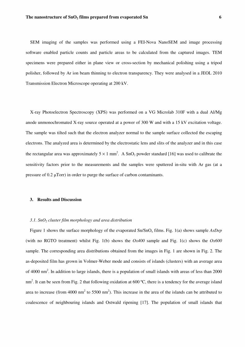
Figure 1 shows the surface morphology of the evaporated Sn/SnOx films. Fig. 1(a) shows sample AsDep
(with no RGTO treatment) whilst Fig. 1(b) shows the Ox400 sample and Fig. 1(c) shows the Ox600
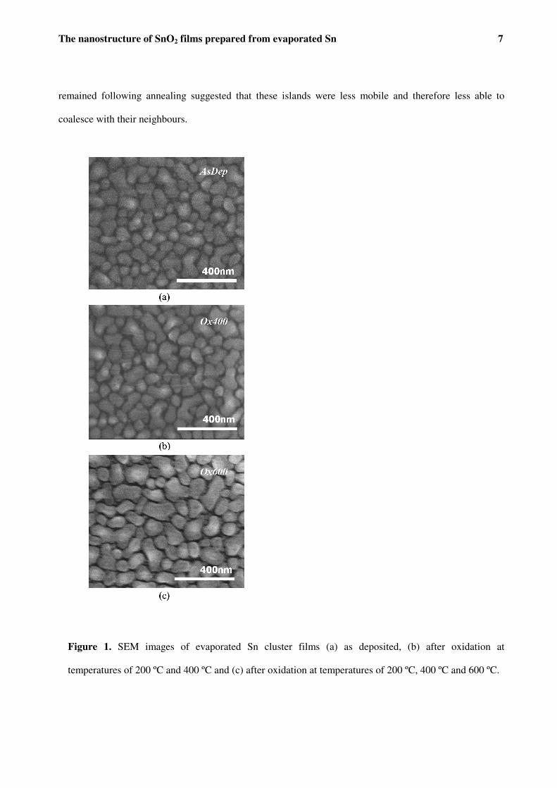
sample. The corresponding area distributions obtained from the images in Fig. 1 are shown in Fig. 2. The
as-deposited film has grown in Volmer-Weber mode and consists of islands (clusters) with an average area
of 4000 nm2. In addition to large islands, there is a population of small islands with areas of less than 2000
nm2. It can be seen from Fig. 2 that following oxidation at 600 ºC, there is a tendency for the average island
area to increase (from 4000 nm2 to 5500 nm
2). This increase in the area of the islands can be attributed to
coalescence of neighbouring islands and Ostwald ripening [17]. The population of small islands that
The nanostructure of SnO2 films prepared from evaporated Sn 7
remained following annealing suggested that these islands were less mobile and therefore less able to
coalesce with their neighbours.
Figure 1. SEM images of evaporated Sn cluster films (a) as deposited, (b) after oxidation at
temperatures of 200 ºC and 400 ºC and (c) after oxidation at temperatures of 200 ºC, 400 ºC and 600 ºC.
The nanostructure of SnO2 films prepared from evaporated Sn 8
Figure 2. Cluster area distributions within thermally evaporated Sn films as deposited (sample-AsDep) and
after oxidation at temperatures of 200 ºC, 400 ºC and 600 ºC (sample-Ox600).
3.2. XPS measurement of stoichiometry
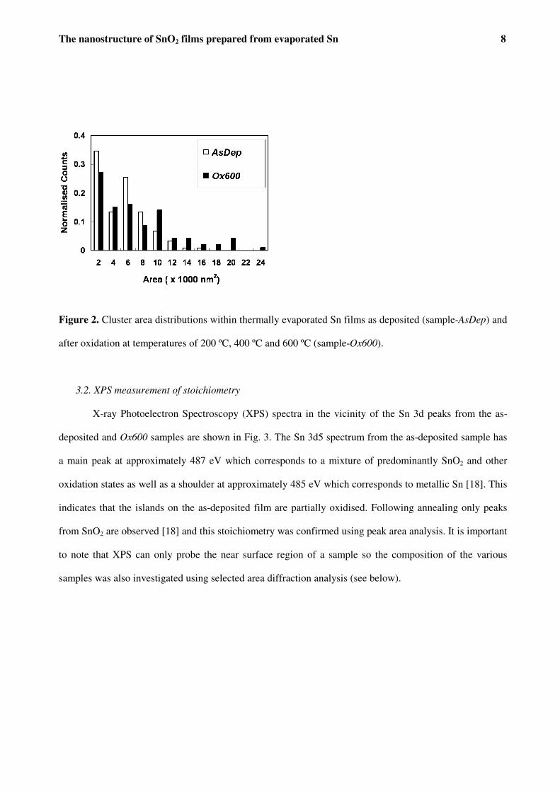
X-ray Photoelectron Spectroscopy (XPS) spectra in the vicinity of the Sn 3d peaks from the as-
deposited and Ox600 samples are shown in Fig. 3. The Sn 3d5 spectrum from the as-deposited sample has
a main peak at approximately 487 eV which corresponds to a mixture of predominantly SnO2 and other
oxidation states as well as a shoulder at approximately 485 eV which corresponds to metallic Sn [18]. This
indicates that the islands on the as-deposited film are partially oxidised. Following annealing only peaks
from SnO2 are observed [18] and this stoichiometry was confirmed using peak area analysis. It is important
to note that XPS can only probe the near surface region of a sample so the composition of the various
samples was also investigated using selected area diffraction analysis (see below).
The nanostructure of SnO2 films prepared from evaporated Sn 9
Figure 3. XPS spectra for evaporated Sn (a) as-deposited and (b) after oxidation at temperatures of 200 ºC,
400 ºC and 600ºC.
3.3. TEM characterization of SnO2 cluster films
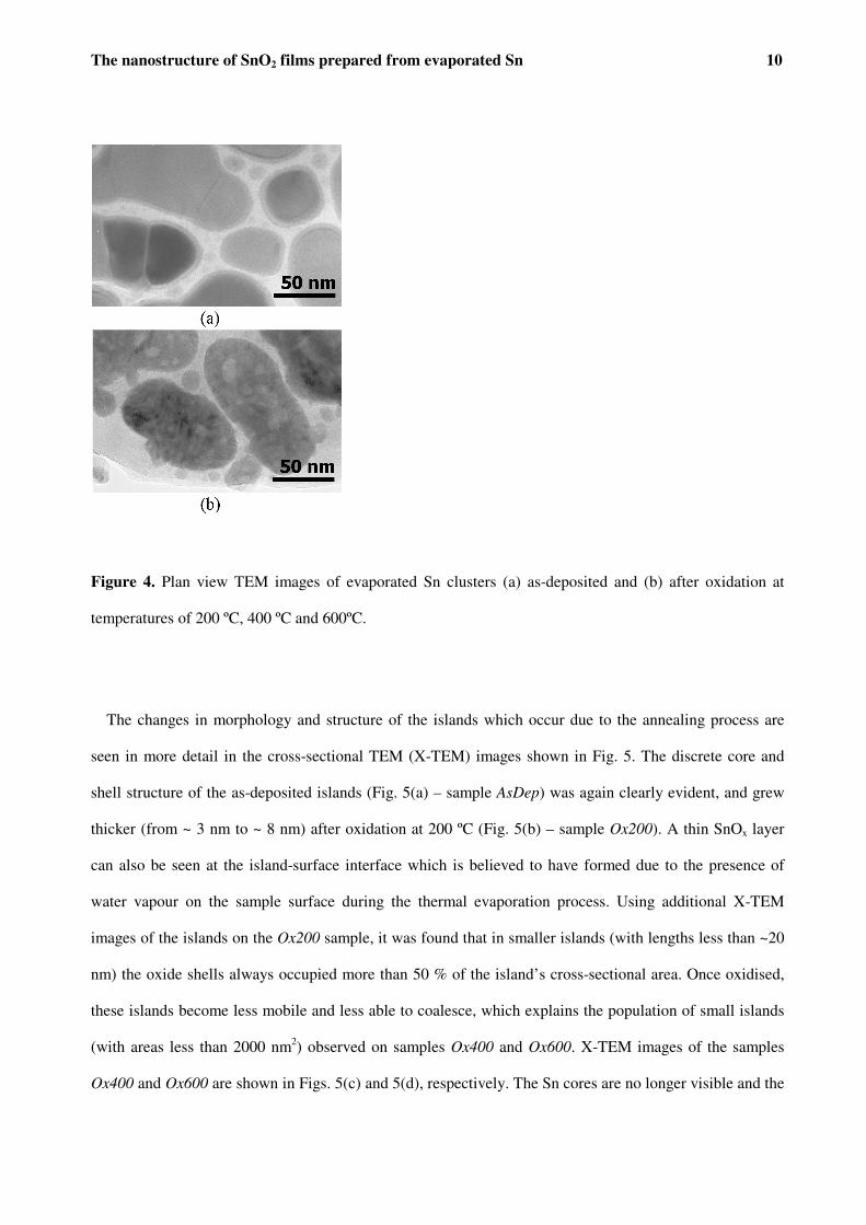
Plan view TEM images of the as-deposited and the sample Ox600 are shown in Fig. 4. The AsDep
sample (Fig. 4(a)) contained irregular shaped islands from 5 nm to 100 nm in length and with heights less
than 30 nm. A thin surface oxide shell (approximately 3 nm in thickness) can also be seen surrounding the
islands. This oxide layer is expected to have grown after the samples were removed from the deposition
system. Following oxidation at 600 ºC, the discrete cores and oxide shells were no longer visible and the
microstructure of the SnOx clusters became more complex, containing small crystallites and voids. Selected
area diffraction patterns from the as-deposited and Ox600 sample (not shown) could be indexed to metallic
Sn and rutile SnO2, respectively. No evidence could be found for metallic Sn reflections in the diffraction
pattern from the Ox600 sample indicating that the Sn clusters had fully transformed into SnO2 following
oxidation to 600 ºC.
The nanostructure of SnO2 films prepared from evaporated Sn 10
Figure 4. Plan view TEM images of evaporated Sn clusters (a) as-deposited and (b) after oxidation at
temperatures of 200 ºC, 400 ºC and 600ºC.
The changes in morphology and structure of the islands which occur due to the annealing process are
seen in more detail in the cross-sectional TEM (X-TEM) images shown in Fig. 5. The discrete core and
shell structure of the as-deposited islands (Fig. 5(a) – sample AsDep) was again clearly evident, and grew
thicker (from ~ 3 nm to ~ 8 nm) after oxidation at 200 ºC (Fig. 5(b) – sample Ox200). A thin SnOx layer
can also be seen at the island-surface interface which is believed to have formed due to the presence of
water vapour on the sample surface during the thermal evaporation process. Using additional X-TEM
images of the islands on the Ox200 sample, it was found that in smaller islands (with lengths less than ~20
nm) the oxide shells always occupied more than 50 % of the island’s cross-sectional area. Once oxidised,
these islands become less mobile and less able to coalesce, which explains the population of small islands
(with areas less than 2000 nm2) observed on samples Ox400 and Ox600. X-TEM images of the samples
Ox400 and Ox600 are shown in Figs. 5(c) and 5(d), respectively. The Sn cores are no longer visible and the
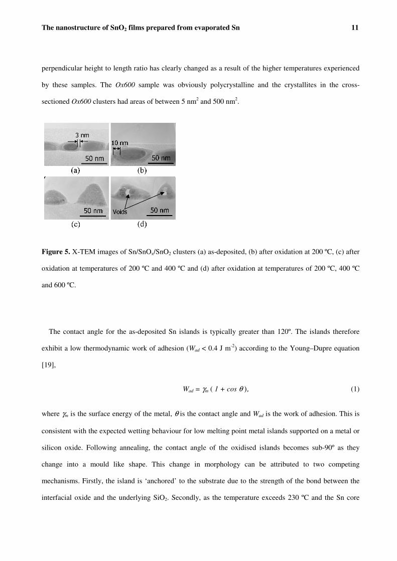
The nanostructure of SnO2 films prepared from evaporated Sn 11
perpendicular height to length ratio has clearly changed as a result of the higher temperatures experienced
by these samples. The Ox600 sample was obviously polycrystalline and the crystallites in the cross-
sectioned Ox600 clusters had areas of between 5 nm2 and 500 nm
2.
Figure 5. X-TEM images of Sn/SnOx/SnO2 clusters (a) as-deposited, (b) after oxidation at 200 ºC, (c) after
oxidation at temperatures of 200 ºC and 400 ºC and (d) after oxidation at temperatures of 200 ºC, 400 ºC
and 600 ºC.
The contact angle for the as-deposited Sn islands is typically greater than 120º. The islands therefore
exhibit a low thermodynamic work of adhesion (Wad < 0.4 J m-2
) according to the Young–Dupre equation
[19],
Wad = γm ( 1 + cos θ ), (1)
where γm is the surface energy of the metal, θ is the contact angle and Wad is the work of adhesion. This is
consistent with the expected wetting behaviour for low melting point metal islands supported on a metal or
silicon oxide. Following annealing, the contact angle of the oxidised islands becomes sub-90º as they
change into a mould like shape. This change in morphology can be attributed to two competing
mechanisms. Firstly, the island is ‘anchored’ to the substrate due to the strength of the bond between the
interfacial oxide and the underlying SiO2. Secondly, as the temperature exceeds 230 ºC and the Sn core
The nanostructure of SnO2 films prepared from evaporated Sn 12
becomes molten, it adopts an energetically favourable sphere-like shape. The surface oxide conforms to the
sphere-like core except at the island-substrate interface where it remains firmly adhered as the energy of
attachment is high for an oxide-oxide interface. The contact angle of the island therefore reduces as a result
of the oxidation process. As the perpendicular height of the fully oxidised islands is significantly greater
than that of the as-deposited islands, the volume of the islands has increased. The average volumetric
change was estimated from the TEM and SEM images to be more than 50 %. Thermally assisted
coalescence of neighbouring clusters and the formation of pores, which were clearly visible in the clusters
of the Ox600 sample, were responsible for the larger than expected volume increase. One explanation for
the occurrence of these voids may be that if the temperature exceeds 400 ºC, any remaining Sn out-gasses
sufficiently to create ‘bubbles’ which cannot escape through the surrounding oxide. Alternatively, they
may be caused simply by thermal expansion and contraction of Sn and/or SnOx within the clusters
occurring as a result of the RGTO process. Some densification of the SnO2 is expected to occur due to
crystallisation at temperatures between 400 ºC and 600 ºC but it is unlikely that this effect alone is capable
of producing voids as large as those seen in the Ox600 sample.
3.4. Gas sensing measurements
The attributes of the SnO2 film which was oxidised at temperatures up to 600 ºC (high surface-area,
nanoscale clusters and pores) suggested that it may be capable of gas sensing. A prototype sensor was
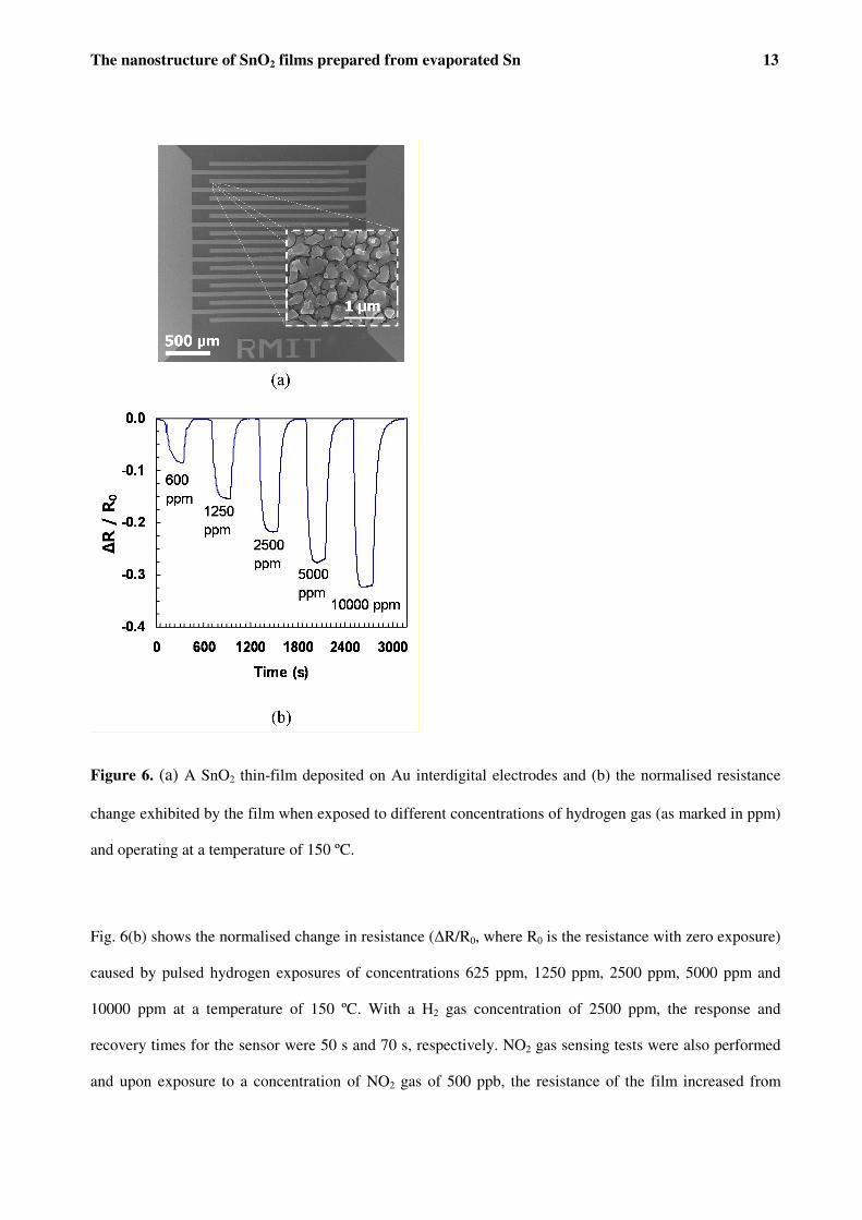
therefore fabricated and tested. Fig. 6(a) shows a SEM image of a RGTO treated SnO2 cluster film
supported on dual inter-digital eletrodes and a passivated Si substrate. As mentioned previously, this film
was produced using two evaporations with RGTO processes following each of the evaporations. TEM
inspection of a small section of the film revealed that the clusters were polycrystalline with similar
nanostructure to that shown in Fig. 5(d). The sensor film clearly has high surface area and appears coral-
like in its morphology (as seen in Fig. 6(a)). Neighbouring clusters are more densely packed in this thicker
film than they are in the films shown in Fig. 1 and the probability of coalescence is therefore higher.
The nanostructure of SnO2 films prepared from evaporated Sn 13
Figure 6. (a) A SnO2 thin-film deposited on Au interdigital electrodes and (b) the normalised resistance
change exhibited by the film when exposed to different concentrations of hydrogen gas (as marked in ppm)
and operating at a temperature of 150 ºC.
Fig. 6(b) shows the normalised change in resistance (∆R/R0, where R0 is the resistance with zero exposure)
caused by pulsed hydrogen exposures of concentrations 625 ppm, 1250 ppm, 2500 ppm, 5000 ppm and
10000 ppm at a temperature of 150 ºC. With a H2 gas concentration of 2500 ppm, the response and
recovery times for the sensor were 50 s and 70 s, respectively. NO2 gas sensing tests were also performed
and upon exposure to a concentration of NO2 gas of 500 ppb, the resistance of the film increased from
The nanostructure of SnO2 films prepared from evaporated Sn 14
8.4 kΩ to 18.9 kΩ. The response and recovery times exhibited for this concentration of NO2 were 50 s and
90 s, respectively. These results compare favourably with previous results for undoped SnO2 thin-film
sensors [4]. We are now planning to use the prototype sensor and TEM to assess whether the structure of
the porous polycrystalline SnO2 film remains stable after long term exposure to NO2 and H2.
4. Summary
The RGTO technique was used to prepare SnOx clusters from discontinuous evaporated Sn thin films.
Samples with different ultimate oxidation temperatures were characterised and the stoichiometry,
morphology and micro-structure determined. Selected area diffraction patterns and TEM images showed
that the as-deposited Sn clusters were polycrystalline with a ~ 3 nm thick native oxide layer and a well
defined inner Sn core. The remaining samples showed that the oxide layer grows to ~ 8 nm thickness after
oxidation for 2-hrs at 200 ºC and the metallic Sn core was no longer evident when the maximum oxidation
temperature was 400 ºC or 600 ºC. XPS and selected area diffraction showed that the clusters oxidised up
to 600 ºC were substantially SnO2, as previously reported and that they were polycrystalline. Crystallites
with cross-sectional areas of between 5 nm2 and 500 nm
2 were seen in these clusters. Whilst the
morphology of the SnO2 cluster film was not dramatically different from the as-deposited Sn cluster film,
the average volume of the SnO2 clusters was significantly larger. Voids were found in many of the SnO2
clusters and undoubtedly contributed to the observed increase in volume. Finally, a prototype sensor based
on RGTO processed thermally evaporated Sn was tested and found to exhibit good sensitivity to H2 and
NO2 gases making them suitable for many commercial applications.
The nanostructure of SnO2 films prepared from evaporated Sn 15
15
REFERENCES
[1] Ihokura K and Watson J 1994 The Stannic Oxide Gas Sensor: Principles and Applications
(Florida: CRC Press)
[2] Schierbaum K D, Weimar U and Goepel W 1992 Sensors and Actuators B 7 709
[3] Kalantar-zadeh K and Fry B 2007 Nanotechnology-Enabled Sensors (New York: Springer)
[4] Lou X, Peng C, Wang X and Chu W 2007 Vacuum 81 883
[5] Shanthi E, Dutta V, Banerjee A and Chopra K L 1980 J. Appl. Phys. 51 6243
[6] Dattoli E N, Wan Q, Guo W, Chen Y, Pan X and Lu W 2007 Nano Letters 7 2463
[7] El Khakani M A, Dolbec R, Serventi A M, Horrillo M C, Trudeau M, Saint-Jacques R G,
Rickerby D G and Sayago I 2001 Sensors and Actuators B 77 383
[8] Pan X Q and Fu L 2001 Journal Applied Physics 89 6048
[9] Micocci G, Tepore A, Serra A, Siciliano P and Ali-Adib Z 1996 Vacuum 47 1175
[10] G Sberveglieri G, G Faglia G, S Groppelli S, P Nelli P and Camanzi A 1990 Semiconductor
Science and Technology 5 1231
[11] Kolmakov A, Zhang Y and Moskovits M 2003 Nano Letters 3 1125
[12] Geurts J, Rau S, Richter W and Schmitte F J 1984 Thin Solid Films 121 217
[13] Park G-S and Yang G-M 2000 Thin Solid Films 365 7
[14] Nelli P, Faglia G, Sberveglieria G, Ceredab E, Gabettab G, Dieguezc A, Romano-Rodriguezc
A and Morante J R 2000 Thin Solid Films 371 249
[15] Aste T, Botter R and Beruto D 1995 Sensors and Actuators B 24 826
[16] Sigma Aldrich SnO2 Prod. no. 244651-100G 99.9% -325 mesh
[17] Ostwald W 1900 Z. Phys. Chem. 34 495
[18] Briggs D and Seah M P (Ed.) 1990 Practical Surface Analysis 2nd
edition Vol. 1 Auger and
Xray Photoelectron Spectroscopy (England: Wiley) p. 642
[19] Howe J M 1997 Interfaces in Materials (New York: Wiley) p. 182
Copyright © 2022 FDOKUMEN


![[2014] 1 LNS 1116 Legal Network Series - SN NAIR](https://static.fdokumen.com/doc/165x107/631780519076d1dcf80bd31f/2014-1-lns-1116-legal-network-series-sn-nair.jpg)