![An EMF Study of LiF-BeF2 Solutions [Disc 3] - Molten Salt ...](https://static.fdokumen.com/doc/165x107/63237dd8be5419ea700ea0fe/an-emf-study-of-lif-bef2-solutions-disc-3-molten-salt-.jpg)
An EMF Study of LiF-BeF2 Solutions [Disc 3] - Molten Salt ...
Upload
independentCategory
view
4download
0
This article appeared in a journal published by Elsevier. The attachedcopy is furnished to the author for internal non-commercial researchand education use, including for instruction at the authors institution
and sharing with colleagues.
Other uses, including reproduction and distribution, or selling orlicensing copies, or posting to personal, institutional or third party
websites are prohibited.
In most cases authors are permitted to post their version of thearticle (e.g. in Word or Tex form) to their personal website orinstitutional repository. Authors requiring further information
regarding Elsevier’s archiving and manuscript policies areencouraged to visit:
http://www.elsevier.com/copyright

Author's personal copy
Applied Surface Science 257 (2011) 3313–3319
Contents lists available at ScienceDirect
Applied Surface Science
journa l homepage: www.e lsev ier .com/ locate /apsusc
Electrical and optical properties of thermally-evaporated thin films fromA2[TiO(C2O4)2] (A = K, PPh4) and 1,8-dihydroxyanthraquinone
E. Carbia-Ruelasa, M.E. Sánchez-Vergaraa,∗, V. García-Montalvob, O.G. Morales-Saavedrac,J.R. Álvarez-Badaa
a Coordinación de Ingeniería Mecatrónica. Facultad de Ingeniería, Universidad Anáhuac México Norte. Avenida Universidad Anáhuac 46, Col. Lomas Anáhuac, 52786, Huixquilucan,Estado de México, Mexicob Instituto de Química, Universidad Nacional Autónoma de México. Circuito Exterior, Ciudad Universitaria, 04510, México, D. F, Mexicoc Centro de Ciencias Aplicadas y Desarrollo Tecnológico, Universidad Nacional Autónoma de México, CCADET-UNAM. A. P. 70-186, Coyoacán, 04510, México, D. F, Mexico
a r t i c l e i n f o
Article history:Received 8 July 2010Received in revised form 1 November 2010Accepted 1 November 2010Available online 10 November 2010
Dedicated to Professor Raymundo CeaOlivares on the occasion of his 60thbirthday.
Keywords:Thin filmsOptical propertiesElectrical propertiesNLO-effect
a b s t r a c t
In this work, the synthesis of molecular materials formed from A2[TiO(C2O4)2] (A = K, PPh4) and 1,8dihydroxyanthraquinone is reported. The synthesized materials were characterized by atomic forcemicroscopy (AFM), infrared (IR) and ultraviolet-visible (UV–vis) spectroscopy. IR spectroscopy showedthat the molecular-material thin-films, deposited by vacuum thermal evaporation, exhibit the same intra-molecular vibration modes as the starting powders, which suggests that the thermal evaporation processdoes not alter the initial chemical structures. Electrical transport properties were studied by dc conduc-tivity measurements. The electrical activation energies of the complexes, which were in the range of0.003–1.16 eV, were calculated from Arrhenius plots. Optical absorption studies in the wavelength rangeof 190–1090 nm at room temperature showed that the optical band gaps of the thin films were around1.9–2.3 eV for direct transitions Egd. The cubic NLO effects were substantially enhanced for materialssynthesized from K2[TiO(C2O4)2], where �(3) (−3ω; ω, ω, ω) values in the promising range of 10−12 esuhave been evaluated.
© 2010 Elsevier B.V. All rights reserved.
1. Introduction
Molecular materials have received an increasing interest dueto their characteristic electrical properties, which may lead tosemiconducting, conducting or insulating behavior [1–3]. Thesematerials are formed from the organization and condensation ofmolecular units that may be organic and metalorganic species.Their microstructure is of particular interest, as they are generallyformed by molecules displaying preferential paths for conduc-tivity [4,5]. The molecules chosen as building blocks to make aconducting solid must lead to a packing that prioritizes the overlapof �-type orbitals in order to generate appropriate energy bandsfor the mobility of the charge carriers, and they must also becapable of giving or accepting electrons with a low energetic cost,so that such bands be partially occupied. Therefore, dependingon the distribution of the molecules within the material and onthe extent of the electronic transfer, different band structures areformed and, consequently, compounds that may be insulating,semiconducting, metallic or superconducting may be obtained. Formany years, most research had dealt with inorganic materials, until
∗ Corresponding author.E-mail address: [email protected] (M.E. Sánchez-Vergara).
the potential of the organic and metalorganic derivatives becameclear when it was reported that the tetrathiofulvalene chloride waselectrically conducting at the relatively low temperatures between50 and 60 K [6,7], and the application of (organo-) aluminumcompounds as thin films for microelectronics was reported [8].In the following years, a lot of effort has been oriented to theformation and characterization of molecular-material thin filmsas an important step towards their use in organic-based devices[9–12]. On the other hand, research on molecular electronicsinvolving transition metal complexes has received an increasinginterest based on the fact that the oxidation states of transi-tion metals can be varied to a great extent and thus that manyelectron transfer processes can result [6,7,13]. Several studies ofmaterials containing metallic complexes have been reported todate [13–18]. Some important examples are the first supercon-ductor with a paramagnetic metal ion, (BEDT–TTF)4A[Fe(C2O4)3](BEDT–TTF = bis(ethylenedithio)tetrathiafulvalene and A = K,NH4, H2O) [17]; the first molecular metallic ferromagnet(BEDT–TTF)3[MnIICrIII(C2O4)3], which was formed by infinitesheets of the magnetic coordination polymer interleaved withlayers of conducting BEDT–TTF cations, and shows ferromag-netism and metallic conductivity [18]. Hybrid compounds basedon dimetallic MIIMIII oxalate complexes (MIII = Cr, Fe; MII = Mn,Fe, Co, Ni, Cu and Zn) and TTF molecules have also been reported
0169-4332/$ – see front matter © 2010 Elsevier B.V. All rights reserved.doi:10.1016/j.apsusc.2010.11.011
Author's personal copy
3314 E. Carbia-Ruelas et al. / Applied Surface Science 257 (2011) 3313–3319
[19], as well as thin films obtained from [TiO(C2O4)2]2− anioniccomplexes and n-octadecylamine [20].
In view of the fact that metal oxalate complexes have demon-strated to be promising building blocks to obtain multilayeredmolecular-based materials, the purpose of this work is to exploreA2[TiO(C2O4)2] (A = K, PPh4) and 1,8 dihydroxyanthraquinone(C14H8O4) and its potassium salt (K2C14H6O4) as building blocksto synthesize molecular material thin films. Thermal evaporationand ellipsometry have been employed in the growth and charac-terization of the thin films, respectively. The refractive indices andabsorption coefficients have been determined for the studied sam-ples, since both parameters are of particular interest in the designand fabrication of optoelectronic devices [21,22]. The optical bandgap and electrical properties, such as the electrical conductivity andactivation energy of the resulting thin films, have also been mea-sured. The third harmonic generation (THG) technique was chosento measure the �(3) values because it allows the measurement ofpure electronic NLO-effects, which are important for semiconduct-ing and photonic applications.
2. Experimental procedure
The raw materials for this work were obtained from commercialsources and used with no further purification. (PPh4)2[TiO(C2O4)2]was obtained from the reaction of K2[TiO(C2O4)2] with (PPh4)Cl inwater. Cyclical-voltammetry experiments were carried out for thestarting material with an Autolab PGSTAT30 system in a conven-tional three-electrode mode. FT-IR spectra were acquired with aPerkinElmer IR spectrophotometer model 282-B using KBr pellets.Fast atomic bombardment (FAB+) mass spectroscopy of the pow-der samples was performed on a 3-nitrobenzyl alcohol support inthe positive ion mode on a Jeol spectrometer, model JMS-SX102A.
For the thin films, FT-IR measurements were obtained with aspectrophotometer Nicolet 5-MX. AFM (atomic force microscopy)images were obtained using a Jeol JSPM-4210 in contact mode,tapping and NSCIS (non-contact silicon cantilevers). Ellipsometricmeasurements were made using a Gaertner Model L117 ellipsome-ter with a He–Ne laser operating at 630 nm. UV–vis absorbancemeasurements were made with a Shimadzu 260 double-beamspectrophotometer. A four-probe press contact method wasemployed to measure the electrical conductivity of the samplewithin a working temperature range between 295 and 450 K. Silverpaint was applied to the sample to form an ohmic contact andthe temperature dependence of the electrical conductivity wasmeasured with a Keithley 230 programmable voltage source and aKeithley 485 auto-ranging pico-ammeter, both PC-controlled. Thetemperature of the sample was measured with a chromel–alumelthermocouple attached to an HP 3421 data acquisitionunit.
2.1. Synthesis
An ethanolic solution of A2[TiO(C2O4)2]·nH2O (A = K, PPh4) wasadded either to 1,8 dihydroxyanthraquinone (C14H8O4) or to itspostasium salt (K2C14H6O4) also dissolved in ethanol. The mix-tures were refluxing for 72 h. The obtained solids were filtered off,washed with absolute ethanol and vacuum dried. The four newproducts were recrystallized in a 1:1 ethanol-water solution givingmaterials A to D.
Material A: 0.8 g (0.87 mmol) of (PPh4)2[TiO(C2O4)2], 0.4 g(1.74 mmol) of C14H8O4. Yield reaction 93%. M.p. 306 ◦C (dec).MS(FAB+, DMSO/EtOH) m/z: 305 [TiO(C14H8O4)]+, 241 [C14H8O4]+,339 [PPh4]+, 77 [Ph] +.
Material B: 0.4 g (1.26 mmol) of K2[TiO(C2O4)2], 0.6 g(2.54 mmol) of C14H8O4. Yield reaction 89%. M.p. 311 ◦C (dec).
MS(FAB+, DMSO/EtOH) m/z: 391 [TiO(C2O4)(C14H8O4)]+, 305[TiO(C14H8O4)]+, 241 [C14H8O4]+, 39 [K]+.
Material C: 0.3 g (0.33 mmol) (PPh4)2[TiO(C2O4)2], 0.2 g(0.66 mmol) of K2C14H6O4. Yield reaction 86%. M.p. 298 ◦C (dec).MS(FAB+, DMSO/EtOH) m/z: 305 [TiO(C14H8O4)]+, 241 [C14H8O4]+,339 [PPh4]+, 77 [Ph] +.
Material D: 0.3 g (0.94 mmol) K2[TiO(C2O4)2], 0.6 g(1.88 mmol) of K2C14H6O4. Yield reaction 88%. M.p. 309 ◦C(dec). MS(FAB+, DMSO/EtOH) m/z: 391 [TiO(C2O4)(C14H8O4)]+, 305[TiO(C14H8O4)]+, 241 [C14H8O4]+, 39 [K]+.
2.2. Thin films preparation
Thin-film deposition was carried out onto 7059 Corning glassslices and (1 0 0) single-crystalline silicon (c-Si) wafers. The Corningglass substrates were ultrasonically degreased in warm methanoland dried within a nitrogen atmosphere. The silicon wafers under-went chemical etching with a p solution (10 ml HF, 15 ml HNO3and 300 ml H2O) in order to remove the native oxide from thesurfaces. To prevent powder products from accumulating on thesubstrate surface, the evaporation source was a molybdenum boatwith two grids. The evaporation temperature in the boat was lowerthan the decomposition temperature of the synthesized materials,about 280 ◦C. All samples were obtained using the same deposi-tion system, with the crucible and substrates disposed in the samegeometry. The base pressure (10−1 Torr) in the chamber before thinfilm deposition and the amount of mass inside the crucible werethe same in all cases. For infrared, AFM and ellipsometric measure-ments, the substrates were oriented along the (1 0 0) direction. Eachsubstrate was made of 200 (S cm) c-Si. For the optical transmissionmeasurements, the substrates were bare 7059 Corning glass slices.The electrical conductivity of the films was studied by means ofa four-probe using 7059 Corning glass substrates coated with fourmetallic strips. These metallic strips acted as electrodes for the elec-trical measurements. In order to get an ohmic behavior betweenthe deposited films and the metallic electrodes, four chromiumstrips were deposited by vacuum thermal evaporation onto theglass slices. Finally, measurements of the cubic NLO-propertiesaccording to the THG-Maker fringes technique were performed inthe glass-substrate coated samples. The experimental setup basi-cally consisted of a Q-switched Nd:YAG laser system (Surelite IIfrom Continuum, �ω = 1064 nm, repetition rate of 10 Hz and a pulsewidth of � ≈ 22 ns), which provided the fundamental wave. Typ-ical pulse powers of 80 �J were filtered in order to irradiate thesamples by means of an f = 50 mm focusing lens, thus peak irra-diances on the order of 1.8 GW cm−2 were achieved at the focalspot on the film samples. This value was slightly below the damagethreshold energy supported by the samples under strong focusedbeam irradiation. The polarization of the fundamental beam (Sor P polarizing geometry) was selected by means of an IR-coatedGlan-Laser polarizer and a �/2-quartz-retarder. A second polarizer,used as an analyzer, allowed the characterization of the THG-response. The third harmonic wave (�3ω = 355 nm) was detected bya sensitive photomultiplier tube placed behind interference opticalfilters centered at 355 nm. The THG-device was previously cali-brated by means of a fused silica plate (�(3) ≈ 3.11 × 10⁻¹⁴ esu, at�ω = 1064 nm), which is frequently used as a NLO-reference stan-dard via the Maker fringes method. The THG measurements wereperformed for incident angles in the range from −45◦ to +45◦.
3. Results and discussion
Starting-material cyclic voltamperograms were recorder in anethanolic solution using LiClO4 (1 M) as support electrolyte and acell with a calomel reference electrode and platinum electrodes

Author's personal copy
E. Carbia-Ruelas et al. / Applied Surface Science 257 (2011) 3313–3319 3315
Table 1IR characteristic bands for powder and thin films (cm−1).
Compound �arm(C–H) �(COO) �arm(C−C) �(C–O) ı(OCO)
A (powder) 3041 1674 1625 1271 778A (thin film) 3043 1674 1625 1273 779B (powder) 3069 1720, 1684 1625 1269 783B (thin film) 3070 1720, 1685 1624 1269 785C (powder) 3063 1671 1624 1266 746C (thin film) 3062 1670 1624 1265 744D (powder) 3044 1720, 1686 1611 1263 753D (thin film) 3047 1720, 1686 1612 1265 750
operating as the working electrode and as counter-electrodes,respectively. They show �Eredox in the range of 0.05–0.9 V for theredox potential between the acceptor and donor, with an oxidationpotential of at least 1.7 V for the organic compound and a reductionpotential of 1.75 V for the titanium complex. These values are in therange established by Saito and Ferraris for promising organic metalmaterials (−0.02 ≤ �Eredox ≤ 0.34 V) [4].
FT-IR spectroscopy was performed on both powder samples andthin films to determine the presence of the representative bondvibration modes of the synthesized compounds and to determineif there were significant chemical changes in these materials dur-ing the thermal evaporation process. The presence of new aromatic�(C–H) and �(C–C) signals around 3070–3040 and 1625–1605 cm−1
in powder samples (B and C) indicate the attachment of thedonor. The �(C O) and �(C–O) bands were found in the rangeof 1720–1660 and around 1270 cm−1, respectively. The valuesfor the characteristic IR bands of the thin films are very closeto those observed for the original powder compounds on potas-sium bromide (KBr) pills (Table 1); this suggests that there wasnot decomposition during the process of getting the thin films, sothey kept their initial chemical structure. The slight modificationsobserved in these values may be due to internal stress produced bythe evaporation process.
Despite the relatively low solubility of the obtained pow-der compounds, the positive-ion FAB mass spectra have shownsignals for [C14H8O4]+ (241 m/z) and fragments containing tita-nium, [TiO(C14H8O4)]+ (305 m/z), [TiO(C2O4)(C14H8O4)]+ (391m/z), confirming the presence of the donor. Signals were alsofound for [K] + (39 m/z) in B–D spectra, and for [Ph]+ (77m/z) and [PPh4]+ (339 m/z) in A and C spectra. All of theobserved signals exhibit the expected characteristic isotropicdistribution patterns. Two approaches might explain the acceptor-donor interaction in these new synthesized materials. First, theinclusion of the donor into the coordination sphere of tita-nium might occur, [TiO(C2O4)2(C14H6O4)]−n, as it was proposedin the complex between titanyl oxalate and 3-hydroxyflavone,[TiO(C2O4)2(C15H9O3)2]−4 [23]. On the other hand, it is alsopossible that a multilayer metallic charge-transfer salt wasformed with an arrangement somehow similar to that of(BEDT–TTF)4A[Fe(C2O4)3] (A = K, NH4, H2O), in which succes-sive layers of BEDT–TTF and layers containing alternating A andFe(C2O4)3
−3 was observed [17], (C14H6O4)xAy[TiO(C2O4)2]·nH2O(A = K, PPh4).
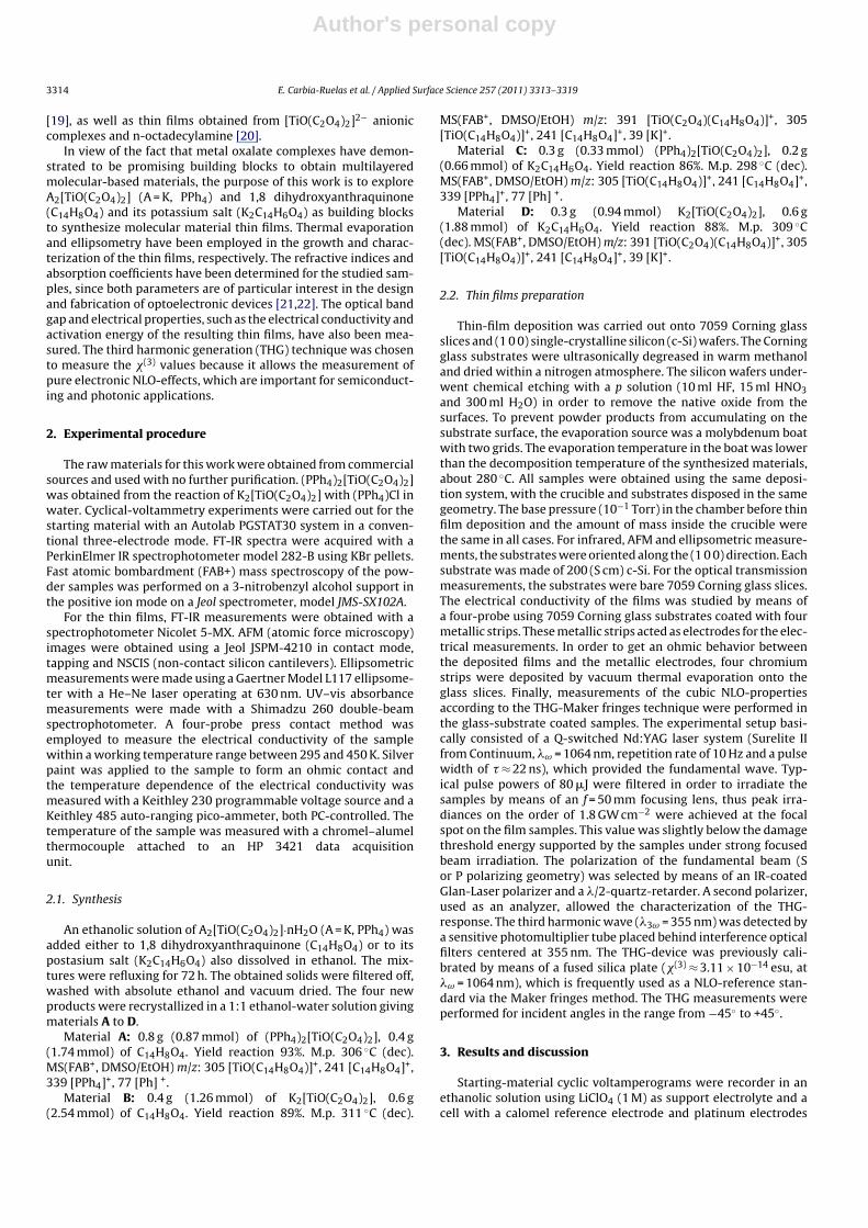
The morphology and roughness of the thin films were exam-ined by atomic force microscopy in order to provide a large surfaceinspection of the micro-structural arrays, topological structure,porosity and film quality of the deposited layers as summa-rized in Fig. 1, where 3D micrographs are shown, and Table 2.For thin-film samples made from materials A and C, one canobserve small-particle agglomeration, a homogeneous distribu-tion and some spots on the surface (Fig. 1A and C). In the caseof films B and D as obtained from K2[TiO(C2O4)2], small parti-cles agglomerate to generate huge rounded grains, showing still areasonably homogeneous distribution at large micrometric lengthscales (see Fig. 1B and D). These latter arrangements show thelargest roughness with small inter-grain porosity (Table 2). It isworth noting that the largest rugosity is shown by films synthesizedfrom the potassium double salt of 1,8-dihydroxyanthraquinone(materials C and D). It is important to point out that the morpho-
Fig. 1. 3D-micrographs obtained by AFM showing the surface morphology of thin films A, B, C and D.
Author's personal copy
3316 E. Carbia-Ruelas et al. / Applied Surface Science 257 (2011) 3313–3319
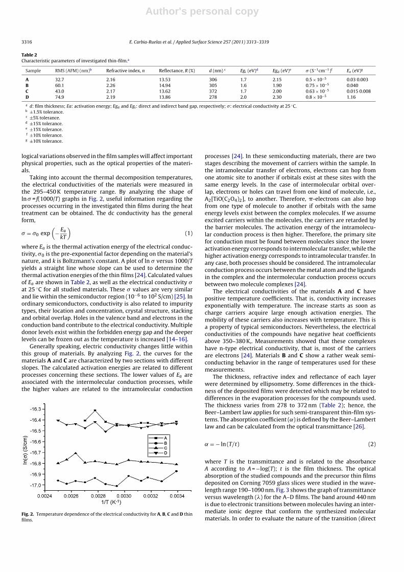
Table 2Characteristic parameters of investigated thin-film.a
Sample RMS (AFM) (nm)b Refractive index, n Reflectance, R (%) d (nm) c Egi (eV)d Egd (eV)e � (S−1cm−1)f Ea (eV)g
A 32.7 2.16 13.53 306 1.7 2.15 0.5 × 10⁻⁵ 0.03 0.003B 60.1 2.26 14.94 305 1.6 1.90 0.75 × 10⁻⁵ 0.040C 43.0 2.17 13.62 372 1.7 2.00 0.63 × 10⁻⁵ 0.015 0.008D 74.9 2.19 13.86 278 2.0 2.30 0.8 × 10⁻⁵ 1.16
a d: film thickness; Ea: activation energy; Egd and Egi: direct and indirect band gap, respectively; �: electrical conductivity at 25 ◦C.b ±1.5% tolerance.c ±5% tolerance.d ±15% tolerance.e ±15% tolerance.f ±10% tolerance.g ±10% tolerance.
logical variations observed in the film samples will affect importantphysical properties, such as the optical properties of the materi-als.
Taking into account the thermal decomposition temperatures,the electrical conductivities of the materials were measured inthe 295–450 K temperature range. By analyzing the shape ofln � = f(1000/T) graphs in Fig. 2, useful information regarding theprocesses occurring in the investigated thin films during the heattreatment can be obtained. The dc conductivity has the generalform,
� = �0 exp(
− Ea
kT
)(1)
where Ea is the thermal activation energy of the electrical conduc-tivity, �0 is the pre-exponential factor depending on the material’snature, and k is Boltzmann’s constant. A plot of ln � versus 1000/Tyields a straight line whose slope can be used to determine thethermal activation energies of the thin films [24]. Calculated valuesof Ea are shown in Table 2, as well as the electrical conductivity �at 25 ◦C for all studied materials. These � values are very similarand lie within the semiconductor region (10−6 to 102 S/cm) [25]. Inordinary semiconductors, conductivity is also related to impuritytypes, their location and concentration, crystal structure, stackingand orbital overlap. Holes in the valence band and electrons in theconduction band contribute to the electrical conductivity. Multipledonor levels exist within the forbidden energy gap and the deeperlevels can be frozen out as the temperature is increased [14–16].
Generally speaking, electric conductivity changes little withinthis group of materials. By analyzing Fig. 2, the curves for thematerials A and C are characterized by two sections with differentslopes. The calculated activation energies are related to differentprocesses concerning these sections. The lower values of Ea areassociated with the intermolecular conduction processes, whilethe higher values are related to the intramolecular conduction
Fig. 2. Temperature dependence of the electrical conductivity for A, B, C and D thinfilms.
processes [24]. In these semiconducting materials, there are twostages describing the movement of carriers within the sample. Inthe intramolecular transfer of electrons, electrons can hop fromone atomic site to another if orbitals exist at these sites with thesame energy levels. In the case of intermolecular orbital over-lap, electrons or holes can travel from one kind of molecule, i.e.,A2[TiO(C2O4)2], to another. Therefore, �-electrons can also hopfrom one type of molecule to another if orbitals with the sameenergy levels exist between the complex molecules. If we assumeexcited carriers within the molecules, the carriers are retarded bythe barrier molecules. The activation energy of the intramolecu-lar conduction process is then higher. Therefore, the primary sitefor conduction must be found between molecules since the loweractivation energy corresponds to intermolecular transfer, while thehigher activation energy corresponds to intramolecular transfer. Inany case, both processes should be considered. The intramolecularconduction process occurs between the metal atom and the ligandsin the complex and the intermolecular conduction process occursbetween two molecule complexes [24].
The electrical conductivities of the materials A and C havepositive temperature coefficients. That is, conductivity increasesexponentially with temperature. The increase starts as soon ascharge carriers acquire large enough activation energies. Themobility of these carriers also increases with temperature. This isa property of typical semiconductors. Nevertheless, the electricalconductivities of the compounds have negative heat coefficientsabove 350–380 K,. Measurements showed that these complexeshave n-type electrical conductivity, that is, most of the carriersare electrons [24]. Materials B and C show a rather weak semi-conducting behavior in the range of temperatures used for thesemeasurements.
The thickness, refractive index and reflectance of each layerwere determined by ellipsometry. Some differences in the thick-ness of the deposited films were detected which may be related todifferences in the evaporation processes for the compounds used.The thickness varies from 278 to 372 nm (Table 2); hence, theBeer–Lambert law applies for such semi-transparent thin-film sys-tems. The absorption coefficient (˛) is defined by the Beer–Lambertlaw and can be calculated from the optical transmittance [26].
˛ = − ln (T/t) (2)
where T is the transmittance and is related to the absorbanceA according to A = −log(T); t is the film thickness. The opticalabsorption of the studied compounds and the precursor thin filmsdeposited on Corning 7059 glass slices were studied in the wave-length range 190–1090 nm. Fig. 3 shows the graph of transmittanceversus wavelength (�) for the A–D films. The band around 440 nmis due to electronic transitions between molecules having an inter-mediate ionic degree that conform the synthesized molecularmaterials. In order to evaluate the nature of the transition (direct
Author's personal copy
E. Carbia-Ruelas et al. / Applied Surface Science 257 (2011) 3313–3319 3317
Fig. 3. Transmittance vs. wavelength for materials A, B, C and D.
or indirect), the relation [27]:
˛hv = A(hv − Eg)n (3)
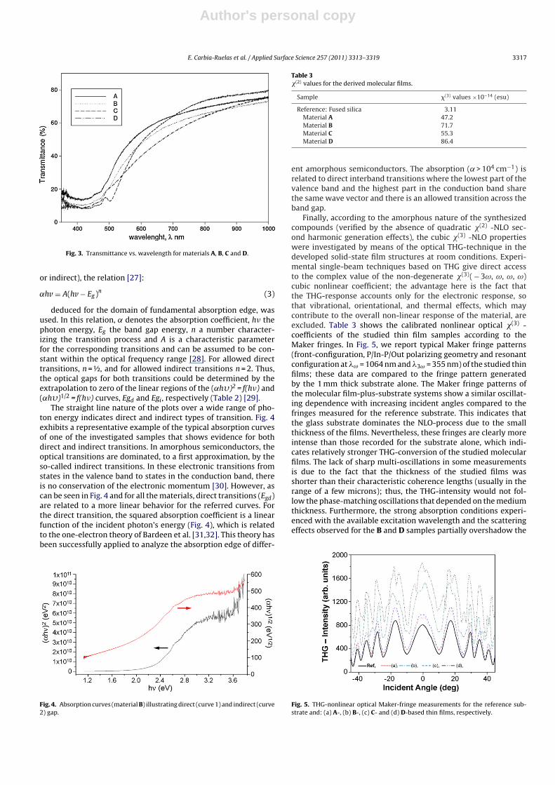
deduced for the domain of fundamental absorption edge, wasused. In this relation, ˛ denotes the absorption coefficient, h� thephoton energy, Eg the band gap energy, n a number character-izing the transition process and A is a characteristic parameterfor the corresponding transitions and can be assumed to be con-stant within the optical frequency range [28]. For allowed directtransitions, n = ½, and for allowed indirect transitions n = 2. Thus,the optical gaps for both transitions could be determined by theextrapolation to zero of the linear regions of the (˛h)2 = f(h�) and(˛h)1/2 = f(h�) curves, Egd and Egi, respectively (Table 2) [29].
The straight line nature of the plots over a wide range of pho-ton energy indicates direct and indirect types of transition. Fig. 4exhibits a representative example of the typical absorption curvesof one of the investigated samples that shows evidence for bothdirect and indirect transitions. In amorphous semiconductors, theoptical transitions are dominated, to a first approximation, by theso-called indirect transitions. In these electronic transitions fromstates in the valence band to states in the conduction band, thereis no conservation of the electronic momentum [30]. However, ascan be seen in Fig. 4 and for all the materials, direct transitions (Egd)are related to a more linear behavior for the referred curves. Forthe direct transition, the squared absorption coefficient is a linearfunction of the incident photon’s energy (Fig. 4), which is relatedto the one-electron theory of Bardeen et al. [31,32]. This theory hasbeen successfully applied to analyze the absorption edge of differ-
Fig. 4. Absorption curves (material B) illustrating direct (curve 1) and indirect (curve2) gap.
Table 3�(2) values for the derived molecular films.
Sample �(3) values ×10−14 (esu)
Reference: Fused silica 3.11Material A 47.2Material B 71.7Material C 55.3Material D 86.4
ent amorphous semiconductors. The absorption (˛ > 104 cm−1) isrelated to direct interband transitions where the lowest part of thevalence band and the highest part in the conduction band sharethe same wave vector and there is an allowed transition across theband gap.
Finally, according to the amorphous nature of the synthesizedcompounds (verified by the absence of quadratic �(2) -NLO sec-ond harmonic generation effects), the cubic �(3) -NLO propertieswere investigated by means of the optical THG-technique in thedeveloped solid-state film structures at room conditions. Experi-mental single-beam techniques based on THG give direct accessto the complex value of the non-degenerate �(3)( − 3ω, ω, ω, ω)cubic nonlinear coefficient; the advantage here is the fact thatthe THG-response accounts only for the electronic response, sothat vibrational, orientational, and thermal effects, which maycontribute to the overall non-linear response of the material, areexcluded. Table 3 shows the calibrated nonlinear optical �(3) -coefficients of the studied thin film samples according to theMaker fringes. In Fig. 5, we report typical Maker fringe patterns(front-configuration, P/In-P/Out polarizing geometry and resonantconfiguration at �ω = 1064 nm and �3ω = 355 nm) of the studied thinfilms; these data are compared to the fringe pattern generatedby the 1 mm thick substrate alone. The Maker fringe patterns ofthe molecular film-plus-substrate systems show a similar oscillat-ing dependence with increasing incident angles compared to thefringes measured for the reference substrate. This indicates thatthe glass substrate dominates the NLO-process due to the smallthickness of the films. Nevertheless, these fringes are clearly moreintense than those recorded for the substrate alone, which indi-cates relatively stronger THG-conversion of the studied molecularfilms. The lack of sharp multi-oscillations in some measurementsis due to the fact that the thickness of the studied films wasshorter than their characteristic coherence lengths (usually in therange of a few microns); thus, the THG-intensity would not fol-low the phase-matching oscillations that depended on the mediumthickness. Furthermore, the strong absorption conditions experi-enced with the available excitation wavelength and the scatteringeffects observed for the B and D samples partially overshadow the
Fig. 5. THG-nonlinear optical Maker-fringe measurements for the reference sub-strate and: (a) A-, (b) B-, (c) C- and (d) D-based thin films, respectively.
Author's personal copy
3318 E. Carbia-Ruelas et al. / Applied Surface Science 257 (2011) 3313–3319
Maker fringe oscillations. Indeed, the THG-response obtained atnearly normal incidence gives the highest conversion efficiency,which permits the relative evaluation of the �(3) -coefficients. Asa first estimation of the cubic NLO-properties of these materials,and considering samples under resonant (absorption) conditions,the determination of �(3) may be approximated by the followingexpression [33]:
�(3)−Film ≡ �(3)−Reference
(2lReference
c
)(˛/2
1 − e−˛lFilm/2
)(IFilm3ω
IReference3ω
)1/2
(4)
where ˛ is the absorption coefficient of the film sample at thethird harmonic free-wave and lReference
c represents the coherencelength of the reference material (∼8 �m). �(3)−Film and �(3)−Reference
are, respectively, the values of the cubic nonlinear coefficients of thefilm samples and the fused silica plate, while IFilm
3ω and IReference3ω are
the peak intensities of the Maker fringe patterns of the film sampleand the reference plate, respectively. In this way, the �(3) value of anew material relative to the value of the reference standard can beobtained; hence, a calibrated result with a high degree of accuracycan be reported.
In principle, both the film and the substrate contribute to thedetected THG-signal (the focal length of the focusing lens is lessthan 50 mm in order to make the air contribution to the THG-signalnegligible; these two contributions must be separately identifiedin order to give a good estimate of the �(3)−Film coefficients). More-over, since the film is deposited only on one side of the substrate,the experimental configuration is asymmetric from a geometricalviewpoint and different relations have been developed in orderto fit respectively the ‘front’ configuration where the fundamentalbeam enters the film, or the ‘back’ configuration, where the filmsstay behind the substrate [34–40]. Under this framework, Table 3shows the �(3)−Film calibrated coefficients according to Equation 3and Fig. 5 (front configuration). The highest cubic NLO-coefficientwas evaluated for the D-based thin-film sample, followed by the B-,C- and A-based thin films, respectively. A substantial decrease of the�(3)−Film value occurs for the samples not containing a potassiumatom in the final product.
It could be verified that the diverse molecular systems pro-duced notable differences in their linear and nonlinear opticalproperties. Particularly, the cubic NLO effects were considerablyimproved in films of materials synthesized from K2[TiO(C2O4)2],i.e. B and D. These samples exhibited higher conjugation degreesand conductivities, lower optical absorption and band-gap val-ues, and apparently adequate electronic multi-level organizations,which were sensitively detected and verified by NLO-THG mea-surements. In addition to the distinctive differences provoked bythe diverse chemical structures and their corresponding physicalproperties on the THG-responses, another correlation attributed tothe thin film structures (variations on the rugosity, see Table 2)could also be established. Despite the observed differences in thefilm thicknesses, the film structures may also play an importantrole regarding the origin and magnitude of the observed THG-signals, as it is observed that the most THG-efficient D- and B-basedfilm samples also show the highest rugosity. In the specific case ofcompound D, its higher conductivity and the delocalization of itsconjugated electronic system assures the largest cubic NLO phe-nomena.
4. Conclusions
Molecular materials from A2[TiO(C2O4)2] (A = K, PPh4) and 1,8-dihydroxyanthraquinone were synthesized. Their thin films weredeposited by vacuum thermal evaporation. According to the IRspectra, they are formed by the same chemical units as those ofthe corresponding synthesized powders. Thus, the thermal evapo-ration process can be, in general, considered as a molecular process.
The substrate temperature is not high enough to provide the nec-essary surface mobility for the molecular units to produce highlyordered crystalline films. On the other hand, the AFM analysisshows that deposition of thin films over the layers occurs despitesome rugosity and that the film depositions were quite uniformand homogeneous, providing trustworthy electrical and opticalcharacterization tests. The thin films of the synthesized molecularmaterials show electrical conductivities at room temperature of theorder of 10−5 (S cm), which suggests a semiconducting behavior.The electron transport in the investigated compounds is stronglyinfluenced by their molecular structures. Thin films produced fromD and B compounds exhibited a larger conductivity which, in com-bination with a higher degree of conjugation of the delocalized�-electron system, allowed the most favorable conditions to gen-erate efficient cubic NLO-effects such as THG. The measurementof cubic-only, non-degenerated � (3) (−3ω; ω, ω, ω) NLO coeffi-cients in all the studied samples, instead of quadratic- � (2) ones,pointed out to predominantly amorphous structured-moleculararrangements. The cubic NLO effects were substantially enhancedfor materials synthesized from K2[TiO(C2O4)2] (B and D) where �(3)
(−3ω; ω, ω, ω) values in the promising range of 10−12 esu have beenevaluated.
Acknowledgments
Financial support from SEP-CONACyT (grant: 82808-J2 and102401) is gratefully acknowledged. The authors acknowledge thetechnical assistance of Carlos Flores Morales, José Chavez Carvayarand Arturo Rodriguez Gomez (IIM-UNAM).
References
[1] F. Wudl, Acc. Chem. Res. 17 (1984) 227.[2] J.R. Ferrraro, J.M. Williams, Introduction to Synthetic Electrical Conductors,
Academic Press, London, 1987.[3] M.R. Bryce, J. Mater. Chem. 10 (2000) 589.[4] G. Saito, J.P. Ferraris, Bull. Chem. Soc. Jpn. 26 (1980) 2141.[5] D. Astruc, Acc. Chem. Res. 30 (1997) 383.[6] F. Wudl, D. Wobschall, E.J. Hufnagel, J. Am. Chem. Soc. 94 (1972) 671.[7] J. Ferraris, D.O. Cowan, V. Walatka, J.H. Perlstein, J. Am. Chem. Soc. 95 (1973)
948.[8] G.B. Stringfellow, Organometallics Chemical Vapor Epitaxy: Theory and Prac-
tice, Academic Press, New York, 1989.[9] R.A. Laudise, C. Kloc, P.G. Simpkins, T. Siegrist, J. Cryst. Growth 187 (1998)
449.[10] J. Caro, S. Garelik, A. Figeras, Chem. Vap. Deposition 2 (1996) 251.[11] A. Figueras, S. Garelik, J. Caro, J. Cifré, J. Veciana, C. Rovira, E. Ribera, E. Canadell,
A. Seffar, J. Fontcuberta, J. Cryst. Growth 166 (1996) 798.[12] S. Molas, J. Caro, J. Santiso, A. Figueras, J. Fraxedas, C. Méziere, M. Fourmigue, P.
Batail, J. Cryst. Growth 218 (2000) 399.[13] H.E. Toma, J. Braz. Chem. Soc. 14 (2003) 845.[14] P. Cassoux, D. De Caro, L. Valade, H. Casellas, B. Daffos, M.E. Sánchez
Vergara, Mol. Cryst. Liq. Cryst. Sci. Technol. Sect. A 380 (2002)45.
[15] M.E. Sánchez-Vergara, A. Ortiz-Rebollo, J.R. Álvarez, M. Rivera, J. Phys. Chem.Solids 69 (2008) 1.
[16] A. Rodríguez, M.E. Sánchez-Vergara, V. García-Montalvo, A. Ortiz, J.R. Alvarez,Appl. Surf. Sci. 256 (2010) 3374.
[17] M. Kurmoo, A.W. Graham, P. Day, S.J. Coles, M.B. Hurtshouse, J.L. Caulfield, J.Singleton, F.L. Pratt, W. Hayes, L. Ducasse, P. Guionneau, J. Am. Chem. Soc. 117(1995) 12209.
[18] E. Coronado, J.R. Galán-Mascarós, C.J. Gómez-García, V. Laukhin, Nature 408(2000) 447.
[19] E. Coronado, J.R. Galán-Mascarós, C. Giménez-Saiz, C.J. Gómez-García, C. Ruiz-Pérez, Eur. J. Inorg. Chem. (2003) 2290.
[20] P. Ganguly, D.V. Paranjape, M. Sastry, Langmuir 9 (1993) 577.[21] M. Sridharan, S.K. Narayandass, D. Mangalaraj, J. Mater. Sci.: Mater. Electr. 13
(2002) 471.[22] P.N. Prasad, D.J. Williams, Introduction to Nonlinear Optical Effects in Molecules
and Polymers, Wiley Interscience, New York, 1991 (Chapter 1).[23] M. Aleksic, S. Blagojevic, D. Malesec, Z. Radovic, J. Serb. Chem. Soc. 65 (2000)
631.[24] S. Sarkar, Y. Aydogdu, F. Dagdelen, B.B. Bhaumik, K. Dey, Mater. Chem. Phys. 88
(2004) 357.[25] M.S. Kiani, G. RMitchell, Synth. Met. 46 (1992) 293.[26] X. Li, H. Zhu, J. Wei, K. Wang, E. Xu, Z. Li, D. Wu, Appl. Phys. A 97 (2009) 341.

Author's personal copy
E. Carbia-Ruelas et al. / Applied Surface Science 257 (2011) 3313–3319 3319
[27] L. Leontie, M. Caraman, M. Delibas, G.I. Rusu, Mater. Res. Bull. 36 (2001) 1629.[28] M.M. El-Nahass, A.M. Farag, K.F. Abd El-Rahman, A A.A. Darwish, Dispersion
studies and electronic transitions in nickel phthalocyanine thin films, Opt. LaserTechnol. 37 (2005) 513.
[29] L. Leontie, M. Roman, F. Brinza, C. Podaru, G.I. Rusu, Synth. Met. 138 (2003) 157.[30] CodyF G.D., in: J.I. Pankove (Ed.), Hydrogenated Amorphous Silicon, Part B,
Optical Properties, Semiconductors and Semimetals, vol. 21, Academic Press,Orlando, 1984.
[31] M.M. El-Nahass, K.F. Abd-El-Rahman, A.A. Al-Ghamdi, A.M. Asiri, Physica B 344(2004) 398.
[32] J. Bardeen, F.J. Slatt, L.J. Hall, Photoconductivity Conference, Wiley, New York,1956, p. 146.
[33] F. D’Amore, A. Zappettini, G. Facchini, S.M. Pietralunga, M. Martinelli, C.Dell’Erba, C. Cuniberti, D. Comoretto, G. Delle Piane, Synth. Met. 127 (2002)143.
[34] F. D’Amore, M. Di Giulio, S.M. Pietralunga, A. Zappettini, L. Nasi, V. Rigato, M.Martinelli, J. Appl. Phys. 94 (2003) 1654.
[35] H. Nakanishi, H. Matsuda, S. Okada, M. Kato, Polym. Adv. Technol. 1 (1990)75.[36] B. Buchalter, G.R. Meredith, Meredith Appl. Opt. 21 (1982) 3221.[37] G.R. Meredith, Phys. Rev. B 24 (1981) 5522.[38] X.H. Wang, D.P. West, N.B. McKoewn, T.A. King, J. Opt. Soc. Am. B 15 (1998)
1895.[39] K. Miyano, T. Nishiwaki, A. Tomioka, Opt. Commun. 91 (1992) 501.[40] D.S. Bethune, J. Opt. Soc. Am. B 6 (1989) 910.
Copyright © 2022 FDOKUMEN