Understanding Undergraduate Students' Conceptions of a Core Nanoscience Concept: Size and Scale
Upload
oxfordbrookesCategory
view
0download
0
Nanotechnology and Microelectronics: Global Diffusion, Economics and Policy
Ndubuisi Ekekwe Johns Hopkins University, USA
Hershey • New YorkInformatIon scIence reference

Director of Editorial Content: Kristin KlingerDirector of Book Publications: Julia MosemannAcquisitions Editor: Lindsay JohnstonDevelopment Editor: David DeRiccoPublishing Assistant: Tom FoleyTypesetter: Deanna Jo ZombroProduction Editor: Jamie SnavelyCover Design: Lisa TosheffPrinted at: Yurchak Printing Inc.
Published in the United States of America by Information Science Reference (an imprint of IGI Global)701 E. Chocolate AvenueHershey PA 17033Tel: 717-533-8845Fax: 717-533-8661E-mail: [email protected] site: http://www.igi-global.com
Copyright © 2010 by IGI Global. All rights reserved. No part of this publication may be reproduced, stored or distributed in any form or by any means, electronic or mechanical, including photocopying, without written permission from the publisher.Product or company names used in this set are for identification purposes only. Inclusion of the names of the products or companies does not indicate a claim of ownership by IGI Global of the trademark or registered trademark.
Library of Congress Cataloging-in-Publication Data
Nanotechnology and microelectronics : global diffusion, economics and policy / Ndubuisi Ekekwe, editor. p. cm. Includes bibliographical references and index. Summary: "This book assesses the state of nanotechnology and microelectronics, and examines many issues, such as climate change, trade, innovation, diffusion, etc, with a theme focused on facilitating the structures for the adoption and penetration of the technologies into developing nations"--Provided by publisher. ISBN 978-1-61692-006-7 (hbk.) -- ISBN 978-1-61692-007-4 (ebook) 1. Nanotechnology. 2. Microelectronics. 3. Technological innovations--Economic aspects--Developing countries. 4. Technology transfer--Developing countries. 5. High technology industries--Developing countries. I. Ekekwe, Ndubuisi, 1973- T174.7.N37325 2010 620'.5--dc22 2010010146
British Cataloguing in Publication DataA Cataloguing in Publication record for this book is available from the British Library.
All work contributed to this book is new, previously-unpublished material. The views expressed in this book are those of the authors, but not necessarily of the publisher.

341
Copyright © 2010, IGI Global. Copying or distributing in print or electronic forms without written permission of IGI Global is prohibited.
Chapter 21
Nanoscience and Nanotechnology in
Latin America
abstract
Latin America (LA) can count some strong research centers with a tradition of research excellence in certain disciplines such as medicine and biology, nuclear technology, metallurgy and materials, among others. Latin American countries have generated networks of researchers across disciplines, centers, etc. within a country, and linking two or more countries in the region (e.g., Argentina-Brazil Bi-National Center for Nanoscience & Nanotechnology, CABN). Additionally, collaborations have extended beyond LA, mainly to the EU and the USA. In general, these programs have been quite successful in the generation of interdisciplinary nanoscience and nanotechnology (N & N) research. The relation between academia and industry has been improving in the last few years, but it is still weak. In particular, funding incentives for N&N efforts have encouraged joint efforts and contributed to new dimensions in collaborations. This chapter reviews the state of nanoscience and nanotechnology in Chile, Brazil, Argentina and Mexico.
Adolfo NemirovskyLatIPnet Inc., USA
Fernando AudebertUniversity of Buenos Aires, Argentina
Osvaldo N. Oliveira Jr.USP, Brazil
Carlos J. L. ConstantinoUNESP, Brazil
Lorena BarrientosUniversidad Metropolitana de Ciencias de la Educación, Chile and Universidad de Chile,
Chile
Guillermo GonzálezUniversidad de Chile, Chile and CEDENNA,
Chile
Elder de la RosaCentro de Investigaciones en Óptica, México
DOI: 10.4018/978-1-61692-006-7.ch021

342
Nanoscience and Nanotechnology in Latin America
IntroductIon
This chapter provides a survey of the status of nanoscience and nanotechnology (N&N) in Latin America (LA), with special focus in the follow-ing four countries: Argentina, Brazil, Chile and Mexico. N&N has already impacted the global economy, and it appears to hold a large economic potential that is just emerging. This, in turn, is bringing together strong interest from govern-ments, academia, industry and investors in the most developed countries and some fast growing economies (China, India, etc.). In fact, according to Lux Research (Lux 2008), global funding in N&N during 2008 reached almost $20 billion with over 40% from governments, about 40% of corporate funding, and over 5% from venture capital contribution. Products incorporating nano-tech reached over $240 billion with about 65% in manufacturing and materials, 25% electronics and IT and 10% in healthcare and life sciences. Lux predicts that nanotech will touch $3.1 trillion worth of products along the value chain by 2015.
Latin America contribution to total investment and N&N products has been growing but still is quite small. For example, Latin American governments’ investment in N&N in 2006 reached just about $50 million (see Table 1).
N&N is a truthfully interdisciplinary endeavor that requires the collaboration of several disci-plines such as physics, chemistry, mechanical and electrical engineering, biology, medicine, etc. This, in turn, has fostered partnerships among researchers and practitioner from various fields of expertise either at the same facility (university, lab, etc.) or from different institutions in academia and industry. An important byproduct of the emergence of N&N is the strong enhancement of multidis-ciplinary collaborations, and LA has not been an exception. In the last few years, the requirement of this field and the steering of funding agencies have fostered the development of networks of researchers from different disciplines and institu-tions, focused around certain topics of N&N such as optical properties of materials, characterization of materials, biosensors, etc. Some of the efforts are
Table 1. Population, income per capita, R&D and N&N expenditure, Science and Engineering (S&E) and N&N articles and patents to residents, for Argentina, Brazil, Chile and Mexico–compared against selected references
Country Population in 2006
(millions)
2006 GNI per capita
(thousands)
2006 R&D spending
(as % GNP)
Government spending (millions)
N&N R&D(estimated
2006)
S&E articles 2005 per
million people
Nanotech publications per million
people (2005)
Patents to residents
per million people (2005)
Argentina 39.1 11.7 0.41 2 79.0 4.6 4
Brazil 189.3 8.7 0.98 27-40 53.1 4.7 1
Chile 16.4 11.3 0.61 10 95.6 4.5 1
Mexico 104.2 12.0 0.40 12 37.8 3.9 1
Spain 44.1 28.2 1.11 50 422.5 35.3 53
China 1,311.8 4.7 1.44 220 31.9 7.5 16
India 1,109.8 2.5 0.85 106 13.3 1.6 1
Japan 127.8 32.8 3.15 975 434.0 48.5 857
USA 299.4 44.1 2.68 1,775 692.7 47.6 244
Source: Kay L. & Shapira P. (2009)GNI is the gross national income per capita at the Purchasing Power Parity (PPP) as defined by the World Bank. PPP exchange rates equalize
purchasing power across different countries. The data has been compiled from various sources [Kay L. & Shapira P. (2009)]
343
Nanoscience and Nanotechnology in Latin America
involving two or more countries of the region. An example is the Argentina-Brazil Bi-National Cen-ter for Nanoscience & Nanotechnology (CABN). The Center organizes international workshops and N&N schools, promoting the cooperation between Brazilians and Argentinean groups.
The study and characterization of nanoscale materials requires a broad range of approaches, materials and tools, and, in particular, of some expensive equipment such as atomic force mi-croscope (AFM), scanning tunneling microscope (STM) and transmission electron microscope (TEM). In some cases a single institution can have some of these facilities, and in many cases national (or international) labs provide shared facilities for expensive equipment. Latin America has suffered from the lack of availability of de-sired required equipment for nano studies. On the other hand, funding has been provided for some national labs, and large facilities, in particular in Brazil (see Table 1).
Nanotechnology is not a product industry but rather as a set of enabling technologies that sup-ports many existing industries (such as electronics, optics, composite materials, pharmaceuticals). Nanotech impact, in general, is broad but not deep in any one product (e.g., nanotechnology has impacted the aerospace industry, for example, by delivering new materials that are lighter and more resistant, but nanomaterials only represent a tiny fraction, by weight, say of an airplane). Lux Research provides the following classification of nano products–according to the amount of “nano stuff” the final product contains (see below, nano-materials are 100% nano, final goods have only a tiny fraction of nanomaterials):
• Nanomaterials: nanotubes, nanoparticles, nanoporous materials, quantum dots, etc.
• Intermediate products: catalysts, coat-ings, composites, nanostructured alloys, solar cells, sensors, etc.
• Final goods: automotive, consumer elec-tronics, cancer treatment, construction, etc.
Also, included as nano-products are the tools for modeling, probing and manipulating structures at nanoscale:
• Nanotools: inspection tools (scanning probe microscopes, electron microscopes), fabrication tools (dip-pen nanolithogra-phy, nanoimprint lithography), modeling software.
Commercialization requires materials manu-factured in a predictable and consistent way at sufficient volumes. Moving from the lab to the market is usually involved, expensive and time consuming. Currently, most of the nano products in the market are for structural applications (ce-ramics, composites, thin films, powders, metals, coating, etc). Additionally, other markets ad-dressed by nanotech include instruments and tools, cosmetics, and various ICT and biotech applica-tions. In LA, commercialization of nano products has been hindered by several weaknesses such as poor links between academia and industry, lack of patents, lack of consistent and agile frameworks for licensing technologies from universities and labs and limited funding. As shown in Table 1 below, the number of patents in N&N per million inhabitants is much lower than that of developed countries. Nevertheless there are encouraging signs in the last few years, most governments in LA are implementing policies for strengthening IP and supporting its commercialization, encouraging entrepreneurship and academia-industry collabo-ration and partnerships. Moreover, some startups have been launched by academic researchers, and some of these companies are entering the US and other markets. Additionally, a few mid to large size companies (e.g., Petrobras, Tenaris, etc.) are strategically investing in nano projects and engaged in collaborations with (local and global) academia and labs.
The interdisciplinary nature of N&N is begin-ning to transform education, not just impacting graduate and undergraduate students in science

344
Nanoscience and Nanotechnology in Latin America
and engineering but also the general population. Science, math and computer literacy–building critical thinking and learning to model and simu-late complex systems-are becoming basic pillars to form our 21st century citizens–allowing people to fully participate of, and contribute to, society (Baum, G., Nemirovsky, A. and Sabelli N., 2008). LA is now responding to this challenge at higher level of education (grad and undergrad levels). For example, Brazil is building its semiconductor industry with strong government support (Ministry of Science and Technology), building key infra-structure (e.g., CEITEC, a foundry and design center in Porto Alegre), and training hundreds of engineers and scientists, engaged with local and global partners from academia and industry. However there still limited efforts in the region in outreach, K-12 education and, in particular, in training and/or retraining the workforce with new skills to build regional advantages to attract (or create new) companies that required skillful and adaptable workers. Nevertheless, there are some recent regional efforts in this direction. For example, the State of Guanajuato (Mexico) is launching an initiative, led by LatIPnet (a not-for-profit organization that leverages the diasporas of Latin professionals in US and EU), for building a N&N-savvy workforce for the 21st century in collaboration with US partners.
nanoscIence and nanotechnoloGy In arGentIna
Argentina has a long scientific tradition that has led three Argentineans to obtain Nobel Prizes: Bernardo Houssay, in Physiology and Medicine 1947, Luis Federico Leloir, in Chemistry 1970 and César Milstein, in Medicine 1984. Obtaining one Nobel Prize in chemistry and two in medicine is not casual. The disciplines with the longest research tradition in the country are, perhaps, Medicine, Biology and Chemistry. Research has been car-ried out in public Universities, and later, when
the National Council of Scientific and Technical Research (CONICET) was created (in the 50´), also in CONICET research institutes.
In the 50´s Argentina decided to build up a new research area on nuclear physics, and that effort remained for decades until reaching its own technology to build Fission Nuclear Plants and produce all the technologies associated for the type of the reactors developed. For that achievement it was required to develop the metallurgy technol-ogy, which was based on physical metallurgy and materials processing. This development in nuclear physics and metallurgy was led by the National Commission of Atomic Energy (CNEA) created in 1950. The research in metallurgy was later spread in the public universities and CONICET Institutes.
Later on, since the 60´s several areas of research have emerged significantly such as semiconduc-tors, electronics, polymers and ceramics, among others. Of course there are other research areas that have been strongly developed in the scientific spectra in Argentina. This historical brief is just to give an idea on how the basic areas that are the foundations of the N&N in Argentina have been developed. More information on the historical development can be found in Schneider, O. & Sanchez, R. (1980) and in Babini, N & De Asua, M. (2003).
During the last two decades, the govern-ment have defined different priority areas for R&D and the funding programs have addressed particularly towards “information technologies, biotechnology, new materials, renewable energy and nanotechnology” (Ministry of Education and Science, Argentina (2006)). Thus, N&N in Argentina have grown strongly from chemistry and materials science supported on the strong tradition in science and the strategic programs developed in the last decades.
The current strength of Science in Argentina is based on a population with a high level educa-tion, the strong tradition and commitment in the Universities for combining education and research, the prospective studies and the oriented research

345
Nanoscience and Nanotechnology in Latin America
funding programs carried out on the last decades. The weakness is related with a still low invest-ment in R&D, that is just ~0.6% GDP (public + private), which does not allow the acquisition of the required equipments, such as electron microscopes for a full structural characterization of nanomaterials. However, the current president Cristina Fernandez de Kirchner has set science as one of the main bases for the economic and social development, thus in 2007 she created the Ministry of Science, Technology and Productive Innovation (MinCyT). Information technology, biotechnol-ogy and nanotechnology have been selected as priority areas, and several grant schemes are being launched for improving the facilities in the stronger R&D Centers and to promote the formation of
consortiums among academic or R&D institutions and industry in order to generate innovations. Moreover, “Innovation” is promoted at different levels, from the MinCyT (see, www.innovar.gov.ar), regional governments and foundations prizes and start up grants (see www.buenosaires.gob.ar/emprende and www.empretec.org.ar/contenido/institucional.php]. This policy has contributed in the last years to introduce projects and innovations in nanotechnology in several companies, not only in international companies such as Tenaris SA, but also in SMEs. It is expected that this policy will be sustained, which would place Argentina as a competitive country in nanotechnology in the next decade.
Table 2. Argentinean research networks on nanoscience & nanotechnology
Network / Main R&D Topics Partners
Nanostructure Materials and Nanosystems• Nano-magnetism and spintronics • Nanostructured thin films • Surface & coatings • Electronic & opto-electronic properties of nanostructured systems • New instrumentation
CNEA-CAB (Bariloche) CNEA-CAC (Buenos Aires) UBA (Buenos Aires) UNC (Córdoba) UNSL (San Luis)
Nanoscience, Molecular and Supra-molecular Nanotechnology and Interfaces• Modeling and computational simulation • Self-assembly and low dimensional systems • Applications of self-assembly films • Applications of nano/meso-structured systems • Development of new methods of nano/micro-fabrication • Nanobiotechnology
UNRC (Córdoba) UNC (Córdoba) CNEA-CAB (Bariloche) CNEA-CAC (Buenos Aires) UNLP (La Plata) UBA (Buenos Aires) UNSL (San Luis)
Design, Simulation and Fabrication of Micro & Nano Devices and Prototypes• Design of a IMS Prototype • Bench mark for the analysis of fluid flow around MEMs • Modeling the electrokinetic flow in microfluidic devices • Ion mobility spectrometry. Models and Analysis of the detections • Molecular wires • Magnetic measurements in mesoscopic systems using MEMS
CNEA (Buenos Aires) CINSO (Buenos Aires) UBA (Buenos Aires) UNSAM (Buenos Aires) INTEC (Santa Fe) UNER (Entre Ríos) IMBECU (Mendoza) UNNE (Corrientes) CNEA (Bariloche)
Bio-nanostructures for Molecular Information Transmission in Neurobiology and Bio-logical Processes
UNC (Córdoba) CIQUIBIC (Córdoba) UNSL (San Luis) UNT (Tucumán)
CINSO: Center for Research in Solids–CIQUIBIC: Center for Biology Chemistry Research-CNEA: National Commission of Atomic Energy-IMBECU: Institute of Medicine and Biology of Cuyo–INTEC: Institute for Technology Development for the Chemistry Industry–UBA: University of Buenos Aires-UNC: National University pf Córdoba-UNER: National University of Entre Rios-UNNE: National Uni-versity of North-East-UNRC: National University of Rio Cuarto-UNSAM: National University of San Martín-UNSL: National University of San Luis-UNT: National University of Tucumán.

346
Nanoscience and Nanotechnology in Latin America
r&d structure-networks
Over the last five years, to accelerate the activity in N&N four research networks have been cre-ated through a special grant scheme that involved the main R&D centers and universities along the country (see Table 2).
The networks have been really successful increasing the quantity and quality of scientific publications and developing innovation and also materials and technologies. Moreover, in the last years the R&D networks have included industrial partners achieving patents and industrial products. The increase in the networking in N&N can be observed in Figure 1, where the nodes represent R&D institutions and the size of these is correlated with the number of publications, and the linking lines represent the joint publications, the larger the number of joint publications the thicker the line. It is observed that the University of Buenos Aires (UBA), the National University of La Plata (UNLP) and the CNEA are the institutions that have the highest activity in N&N. Some institutions, such as the Institute for Theoreti-cal and Applied Research in Physics-Chemistry (INIFTA), the National University of Córdoba (UNC) and the National University of Mar del Plata (UNMDP), have notably increased their activity in N&N. Moreover, it is observed that not only have increased the links among the R&D institutions, but also new institutions have started developing R&D in N&N. From 2000 to 2008 the number of institutions that have activities in N&N has increase from 46 to 67 (Ministry of Science, Technology and Productive Innovation, Argentina, 2009).
In order to extend the N&N networks to the international community the “Argentine-Brazil Binational Center for Nanoscience & Nanotech-nology” (CABN) has been created. The CABN organizes international workshops and N&N schools, promoting the cooperation between Bra-zilian and Argentinean groups (see http://cabnn.mincyt.gov.ar). Moreover, the International Coop-
eration Division of MinCyT created the Argentine Bureau for Enhancing Cooperation (ABEST) with the European Community. The aim of this Bureau is to establish a platform in Argentina in order to improve and expand cooperation activities in the science, technology and innovation area both with the European Union and with its member states. ABEST has been helping research groups and, small and medium sized local enterprises to participate in the FP6 and FP7 European R&D programs, where one of the main areas is N&N (see http://www.abest.mincyt.gov.ar).
Another strong collaboration in N&N is with USA with whom a declaration for R&D coopera-tion in N&N has been signed. A first workshop in Nanobiotechonology, Inorganic Nanomaterials, Surface & Channels and Dynamic of Materials has already taken place. The program includes student and researcher exchanges and fosters a long cooperation carrying out R&D programs in Nanomaterials (see: cooperación internacional in http://www.mincyt.gov.ar).
Cooperation programs in N&N are also in-volved in recent agreements for cooperation in R&D in Materials Science and Engineering, signed with the University of Oxford, United Kingdom, and with the Leibniz Institute for Solid State and Materials Research, Dresden, Germany.
r&d centers and funding sources
The government’s strategic plan for developing a strong R&D structure enables Argentina to play an important international roll in N&N, and besides the building of N&N networks, the plan includes (i) a grant scheme for providing equipments to the existing R&D groups that have joint research projects; and (ii) the creation of the “Argentine Foundation for Nanotechnology” (FAN).
The grants for acquiring equipments allowed upgrading several existing equipments and the acquisition of new ones. However there is still a lack of state of art high resolution microscopes, such as Field Emission Transmission Electron

347
Nanoscience and Nanotechnology in Latin America
Figure 1. Networks of Argentinean R&D institutions with activity in nanoscience and nanotechnology; (a) network in 2000, (b) network in 2008 (Ministry of Science, Technology and Productive Innovation, Argentina, 2009)

348
Nanoscience and Nanotechnology in Latin America
Microscopes (FEG-TEM) with aberration cor-rectors and FEG Focus Ion Beam equipments. The improvement in the facilities has given an important impulse in the R&D activity in N&N. Therefore, it is expected that new grants for ac-quiring equipments in the next years will provide sufficient budget for acquiring high cost facili-ties, which will allow producing higher impact research in N&N.
The Argentine Foundation for Nanotechnol-ogy (FAN) has been created in 2005 as Private Institution that has as its main objectives (i) to promote the development of technical and human infrastructure in micro- and nanotechnology in Argentina; and (ii) to promote the industrialization with high economic impact of nanomaterials and nanotechnologies. The FAN provides grants to projects for industrializing and commercializing nano- and micro- products or processes that have a high innovation grade and produce an important social and economic impact. It also promotes other activities providing financial support for organizing conferences and meetings. The FAN has already organized two workshops at “MERCOSUR” level where scientists and companies come together with the aim of evaluating the possibilities for increas-ing the micro- and nanotechnology transfer to the industrial sector (see www.fan.org.ar).
In the last years, perhaps due to the influence of the grants schemes, some institutions have built real and virtual R&D Centers on N&N. Some of these Centers are:
CNEA, INN, Institute for the N&N: this virtual institute is composed of several internal laboratories and R&D departments with facilities and R&D working topics related to N&N. Some of those topics are:
• synthesis of nanostructured materials,• surface funcionalization,• nanostructured superconductors,• magnetism at nanoscale,• modeling of magnetic and electronic
properties,
• acoustic photon engineering,• electronic transport in nanoscopic systems,• coatings,• molecules adsorption,• MEMs.
INTI, Industrial Nanotechnology: the Na-tional Institute of Industrial Technology (INTI) is a governmental institute composed by several Departments and Centers with different laborato-ries. The activities of the INTI are related to the industrial sector, providing technical assistance, developing technologies and accreditation service among other duties. Some of the internal labora-tories have merged to form a virtual institute of nanotechnology, with the following topics:
• nanotechnologies for developing materials,• integration on nano- and micro-systems,• surface modification for metallic
biomaterials,• polymer based nanocomposites,• nano- and micro-systems of controlled
release,• nanometrology and nanotextile materials.
CIDIDI, Center for Research, Development, Innovation and Engineering Design: this center has been created recently by agreement between the Faculty of Engineering, University of Buenos Aires (FIUBA) and the Buenos Aires City Government (GCBA). Scientists from FIUBA, industrial part-ners and government come together in the CIDIDI aiming to develop innovations. Its organization involves an advisory board composed by industrial and financial sectors. Thus the three main actors for developing innovations are working together. The building is still under construction and the Center will be fully opened on mid 2010. The R&D laboratories will contain the state of art equipments for nanomaterials development. The facilities will involve a modeling and simulation laboratory, a solidification laboratory with equipments for rapid solidification, a materials characterization lab with

349
Nanoscience and Nanotechnology in Latin America
high resolution scanning and transmission micro-scopes with field emission gun and several detec-tors, machining and metrology labs. The scheme of the organization includes also the majority of the R&D laboratories and workshop belonging to the FIUBA and the Metropolitan Design Center (CMD). The CIDIDI is an innovative concept where scientists work together with designers.
Currently, there are around 70 R&D institutions that have activities in N&N, among them are some Institutes that were created in association between the CONICET and one university or a research institution [Consejo Nacional de Investigaciones Científicas y Técnicas, Argentina. (2009)], such as:
• CETMIC: Center of Technology of Minerals and Ceramics which is associ-ated with the Council for the Scientific and Technical Research of the Buenos Aires Province (CIC);
• CIDEPINT: Center for R&D in Paint Technology which is associated with the CIC;
• CIOP: Center for Optical Research which is associated with the CIC;
• CINSO: Center for Research in Solids which is associated with the IDETEF;
• IFFAMAF: Institute of Physics which is associated with the National University of Córdoba (UNC);
• INFITA: Institute for Theoretical and Applied Research in Physic-Chemistry which is associated with National University of La Plata (UNLP);
• INQUIMAE: Institute of Chemistry and Physics of Materials, Environment and Energy which is associated with the UBA;
• INTECIN: Institute of Technologies and Engineering Science which is associated with the FIUBA;
• INTEMA: Materials Science and Technology Research Institute which is as-sociated with the National University of Mar del Plata.
The Innovation is strongly promoted through two basic grant schemes, one based on companies associated with R&D academic groups, and anoth-er based on academic research with industrial part-ners. Another promoting activity is the “Innovation Competitions”, which are sponsor by an agency of the MinCyT, “Innovar”. From these financial instruments, innovations on nanotechnology have been generated, such as: (i) Pd Catalyst for mo-lecular synthesis for pharmaceutical purposes, and for hydrogen release from methanol in fuel cells; (ii) intelligent paints containing nanoparticles that just release ions in aggressive environments in order to form a passive film; (iii) microvalve for ocular pressure control; (iv) nanocapsules anti-toxoplasmosis; the nanocapsule transports the drug where is the parasite is using 1000 times lower quantity of the doses; (v) electronic noses based on SnO2 thin film; it is suitable for using in several Industries, for instance Argentinean beer breweries and mate tea companies are start-ing to use this equipments [INNOVAR Catalog, (2007); INNOVAR Catalog, (2008); Vago, M. et al., (2008); www.e-nose.com.ar].
r&d areas in nanoscience and nanotechnology
Academic Sector
In Table 2 is summarized the information about the main R&D topics and the partners of the four networks on N&N. There can be observed that no more than 20 groups are involved in the networks. In comparison with the information provided in Figure 1.b, it is worth noting that there are around 50 other institutions/universities working in N&N that are not involved in the networks. The whole contributions of all the groups to the N&N can be classified in: Fundamental Research in Physics & Chemistry, Pharmacology & Medicine, Particles & Materials Development and, Micro- & Nano- Engineering and Technology. The integration of the knowledge development chain from the basic

350
Nanoscience and Nanotechnology in Latin America
research to the technology suggests a great ability to generate innovations steadily on the next decade (Ministry of Education and Science, Argentina, (2004); Malsch, I., (2008)).
Among the several research topics in N&N developed in Argentina, some of high impact and/or strong activity can be mentioned. For instance, there are many groups working on carbon nano-tubes (CNTs):
1. Production of CNTs and development of polymer-based composites using resins resis-tant to alkalis and fire, or using biodegradable polymers. Many groups are involved, affili-ated to the CNEA Buenos Aires, Faculty of Natural and Exact Science–UBA, INTECIN and INTEMA.
2. Development of metal-matrix compos-ites reinforced by CNTs. Recently, the Advanced Materials Group (GMA), Faculty of Engineering, UBA, have launched a joint project with theUniversity of Oxford and with a Belgium company, NANOCYL.
3. Single wall CNTs funcionalization for biomedical application. There is a group working in this topic in the INTEMA.
4. Application of CNTs to sensors. On this topic two groups have been found, one in
the INQUIMAE and other in the CNEA Bariloche.
Groups at CNEA Bariloche, CNEA Buenos Aires and in the Physics Department, UNT, are working on oxide nanowires (NWs). They study the fabrication processes, magnetic and electric properties for batteries, sensors, field effect transis-tors, and energy harvesting devices. In particular, photovoltaic devices employing semiconductor nanowires have the potential for lower cost and greater energy conversion efficiency compared to conventional thin film devices due to less material utilization, enhanced photovoltage or photocurrent. Of particular interest are coaxial structures, such as the GaAs nanowire array shown in Figure 2.a, in which a doped nanowire core is surrounded by a shell of opposite doping type, forming a core-shell p-n junction [Caram, J. et al., (2009)]. Another type of nanowire, the one of ZnO, is promising for the development of third generation solar cells, trans-parent electronics and photonics, spintronics, en-ergy harvesting and sensor applications. The group at UNT is producing and studying these types of NWs. In Figure 2.b is shown a secondary electron image of ZnO NWs grown on a Au nanocluster seeded in a SiO2 substrate by the vapour transport method [Comedi, D. et al., (2009)].
Figure 2. Array of nanowires (secondary electron images). (a) GaAs [Caram, J. et al., (2009)]; (b) ZnO [Comedi, D. et al., (2009)]

351
Nanoscience and Nanotechnology in Latin America
Magnetism and magnetic amorphous & nano-structured materials are other areas with a strong activity, for example,
1. CNEA Bariloche: Some groups study films of magnetic oxides obtained by spray py-rolysis and magnetic properties on different geometries of nanomaterials (nanoparticles, thin films, multilayers), among other specific topics.
2. CNEA Buenos Aires: There is a group that synthesize by means of several techniques (sol gel, microwave or citrate) mixed man-ganese oxide nanoparticles coated by SiO2 for cancer therapies.
3. IFFAMAF: in this institute are groups study-ing magnetic properties of nanoparticles, nanostructured thin films, zeolites, mag-netoresistance and piezoelectric properties of composites such as BaTiO3–BaFe12O19, memory effect on hematite nanoparticles, bulk magnetic metallic glasses, finemet and Nd-Fe-Al alloys.
4. INQUIMAE: there molecular magnets are studied. They prepare molecules and nanoparticles that behave as permanent magnets and also measure characteristics properties of molecular systems that react to the light and environmental conditions.
5. INTECIN: In this institute associated to the Faculty of Engineering, UBA there are two groups that investigate magnetism. The group at the Chemistry Department prepares and studies ferrites for different applications (electronic, ferrofluids and biomedical). The other group associated with the Physics Department has a long experi-ence in magnetic materials. At present they are studying soft magnetic nanostructured alloys; nanocomposites containing soft or hard magnetic particles prepared by gel casting technique; magnetic nanoparticles and nanowires for several applications (medical therapy, drug delivery, sensors);
Nd-Fe-B alloys for magnets and thin film magneto-resistive nanostructured alloys for biosensors and memory devices. It is worth mention that this group has submitted a project to FAN for industrial applications of magnetic nanomaterials joint to Electropart Córdoba S.A.
6. INTEMA: In this Institute are some groups that study soft ferrites nanoparticles for magnetic storage and magneto-optic sensors, among other specific topics.
7. UNLP: One group in the Physics Department has a long tradition in research on mag-netisms & magnetic materials. They are studying metallic and oxide nanoparticles, of various geometries such as ribbons and thin films. A good example of their recent research on magnetostrictive bimagnetic trilayer ribbons for temperature sensing can be found in reference (Mendoza Zélis, P., Sánchez, M., Vázquez J., (2007)).
The networks have addressed the R&D ac-tivities targeting certain applications, mainly to sensors, catalysts and different devices. Thus, strong research topics are being developed in nanoparticles, nanopores and thin films. Some of these topics are:
• Study of adhesion of Ag nanoparticles on textile fibers to kill bacteria. This is sought for items of surgery. It seeks to improve adhesion of Ag nanoparticles that do not fall off during washing. This research is led by INQUIMAE and the company Nanotek.
• Encapsulation of nanoparticles in meso-pores of oxide materials. This research focuses on the development of materials for controlled diffusion of nutrients and metabolic products, and simultaneously acts as a barrier for other metabolic agents; (INQUIMAE).
• Study of elastic polymer-based nanocom-posites containing conductive nanopar-

352
Nanoscience and Nanotechnology in Latin America
ticles for developing pressure sensors. As the pressure increases, the electric perco-lation between particles enhances, which increases the electric current in the nano-composite film; (INQUIMAE).
• Study of core-shell nanoparticles biosen-sors, produced on gold nanoparticles, for diabetes diagnosis; (INQUIMAE-CNEA Bariloche).
• Design of nanomaterials for photo-remedi-ation and photo-therapies. When colorant molecules are irradiated active oxygen molecules (O2*) are formed (Figure 3.a). These active molecules can be used for re-moving chemical and biological contami-nants. Led by INQUIMAE researchers, an automatic self-assembler machine has been developed in order to assemble mol-ecules layer by layer with a good control at the nanoscale (Figure 3.b). This work has been awarded as innovation in 2007.
• Development of nanofilter membranes and mesoporous films for photovoltaic cells, selective sensors and smart windows; (Chemical Department, CNEA Buenos Aires).
There are other important research topics developed by the N&N networks. One is in ma-
terials for solid oxide fuel cells, and the second one is on nanostructured Aluminium alloys for mechanical applications. The most active group in nanoceramics for fuel cells is the CINSO. This group is part of one of the networks that also works on materials for sensors.
They synthesized electrolyte solid solutions of the ZrO2-Y2O3, ZrO2-CaO y ZrO2-CeO2 sys-tems with a wide composition range using the gel-combustion method. Also, they synthesized nanostructured dense ceramic based on ZrO2 (ZrO2-Y2O3 y ZrO2-CaO) or on CeO2 (CeO2-Sm2O3 y CeO2-Y2O3) by “fast firing”, which avoid grain growth. Complementarily they study (La;Sr)CoO3 and (Sm;Sr)CoO3 perovskites for cathode and homogeneous ZrO2-CeO2 solid solutions for the anode. In the case of the anode, it is necessary to prepare composed materials with metals such as Ni or Cu to get a better electronic conductivity. Electrodes are prepared from nanocrystalline powders as conductive pastes which are deposited on the electrolytes and later sintered. The Y2O3 or CaO doped ZrO2 or Sm2O3 or Y2O3 doped CeO2 nanostructured ceramics are used as solid elec-trolytes; cobaltites based materials for cathode and compound materials: Ni/ZrO2-CeO2 for the anode. Two SOFCs configurations are tested: conventional two-chambers and one-chamber fuel cell. The later cell uses the environmental O2 to
Figure 3. (a) Representation of the active oxygen molecule release by the irradiation effect on the colo-rant molecules; (b) Self-assembler machine. [INNOVAR Catalog, (2007)]

353
Nanoscience and Nanotechnology in Latin America
produce the partial oxidation of the hydrocarbon and then, the O2- ions coming from the electro-lyte react with the H2 and the CO, generating H2O and CO2, respectively. The interest in using a one-chamber cell (operated with air and CxHy mixtures as fuel) arises from the fact that the par-tial oxidation of hydrocarbons can be produced at intermediate temperatures (enabling to reduce the usual high operation temperature of SOFCs), (Figure 4). The CINSO group, since 1981, has obtained twenty patents.
Another group in CNEA Bariloche is also working on ceramic materials for fuel cells. In UBA, there are two groups working on this topic, the one in the Chemical Engineering Depart-ment is studying the chemical reactions, and the one in the Mechanical Engineering Department is developing a SOFC in order to test the new nanoceramic materials. Both UBA groups col-laborate with CINSO.
With regard to the nanostructured aluminium alloys for mechanical applications, there are three groups, two of which work on the nanoprecipita-
tion in conventional Aluminium alloys. One group is at the CNEA Bariloche and the other is at the Institute of Physics of Materials (IFIMAT), Tandil. The third group is the Advanced Materials Group (GMA) at the Faculty of Engineering, UBA that has been working on the development of nano-structured light alloys over the last 15 years. The study has involved molecular dynamic simulation and experimental research to understand the role of several elements in the melt and in the undercooled liquid during the rapid solidification (Audebert F. et al., (2001); Audebert F., (2005); Saporiti F., (2009)). A strong collaboration with the Depart-ment of Materials, University of Oxford, allowed the group to have access to electron microscopes and to an unique state-of-the-art research facilities. The collaboration has been extremely successful, with development of “nanoquasicrystalline Al-based alloys” with high thermal stability (Figure 5) and high strength at elevated temperatures (275 MPa at 350°C), typically 5 to 6 times higher than the strongest commercial Al alloys (Audebert F. et al., (2002); Galano M. & Audebert F. et al, (2008)
Figure 4. Experimental one-chamber IT-SOFC built at CINSO operated with garbich gases as fuel [De Reca, W., (2007)]

354
Nanoscience and Nanotechnology in Latin America
and (2009) part I & II). These alloys can compete with Titanium alloys in the medium temperature range (100 to 400°C), which is relevant consid-ering the Ti price is ~30 times more expensive than Al. They are now working in collaboration with the University of Oxford and an industrial consortium (including Rolls Royce and racing car designers) in a project for industrializing these alloys. Two prototypes, compressors for gas turbines and pistons for racing cars, will be developed. A patent on metal-matrix composites (Smith G.W., (2007)) has been achieved, and the group has begun designing new complex metal-matrix nanocomposites with better set of proper-ties in order to enhance the technical feasibility to substitute titanium products.
Industrial Sector
Some companies are interested in participating in a platform for nanomaterials and nanotechnol-ogy development together with the Argentinean research groups: NANOTEK, IAPEL SA, ESSEN SA, Metalúrgica Tandil SA,TENARIS SA [Malsh I., (2008)].
NanotekAn entrepreneur from the petroleum sector and an academic started Nanotek in 2006 as a spin-off from an academic group which had been devel-oping a catalytic process since 2000. The aim of the enterprise is to identify potential applications: “Nanosolutions to megaproblems”. 2007 was the first year they had a turnover. The company has developed process: NanoCatox® and ChlorOff®; materials: NanoKupro®, NanoArgen® and NanoFe®, and products: DusTek®, SoilTek® and Asepsis Klima®.
The NanoCatox® process is based on Fenton reactions. It is validated for removing wastes from celluloses pulp, food processing, petrol and petrochemical, photographic wastes, etc. They build a pilot scale process of 3 liters and the client must upscale it. The process takes place inside an industrial reactor. They are extending the use of the process to contaminated sites; it is already ap-proved for PCBs. The reaction products are Carbon Dioxide, Water and Ferric Oxide. The catalyst is nanometallic iron. One of their projects is aimed at treating contaminants including PCBs with iron-oxide nanoparticles in Paraguay. They have a large home market, because under Argentinean
Figure 5. Improvement in the microstructure stability. Both alloys had a similar microstructure as rapid solidified sample /similar to (b). After 66 hs at 400°C, (a) Al-Fe-Cr alloy shows coarsening, precipitation and quasicrystal transformation, however, (b) the microstructure of the improved alloy remains without any changes. [Galano M. & Audebert F., (2008)]

355
Nanoscience and Nanotechnology in Latin America
law, all PCB contaminated soils must be cleaned before 2010. They also want to develop a method for selective entrapment of heavy metals including lead. This is required due to local regulations in a mining company.
They cooperate with a university for develop-ing an antimicrobial paint using silver nanopar-ticles. Together with the Paint Company Vilba SA they have developed an antimicrobial latex (Asepsis Klima®). The company also intends to apply silver nanoparticles in polymeric blends as biocide and fungicide for food preservation. Moreover, they also have an initial agreement for a project developing filters, containing silver nanoparticles for air-conditioners in cooperation with a Spanish partner. There is another project at lab scale with INQUIMAE and a manufacturer of specialty textiles for adding silver nanoparticles.
The company is also starting collaboration with the Autonomous University of Barcelona with the aim of enhancing the response of biosensors with metallic nanoparticles or thin films such as copper, silver and iron. Furthermore, they are starting work on zinc nanoparticles and zinc oxide for non-toxic UV barriers in cosmetics (Malsh I., (2008)).
Iapel SAThis Company produces pistons, and is specialized in forged pistons for racing cars. They are also active in the international market. This company collaborates with GMA to develop forged pistons for racing cars using nanostructured Al-based al-loys. They are involved, together with GMA, in two international projects.
Metalúrgica Tandil SAThis metallurgy company has cooperated with a research group at IFIMAT for improving the alloy configuration and treatment to enhance the mechanical properties and control the nanopre-cipitation.
Essen SAThis company cooperated with GMA for devel-oping wear resistant nanocoatings on Aluminium products.
Tenaris SAThis is an Argentinean international Company that produces seamless tubes for the petroleum industry. The Company has an important R&D sector, with laboratories in Argentina, Mexico, Italy and Japan. The main R&D laboratory is in Argentina; they are generating innovations since many years ago and use N&N mainly on coatings for tribological and corrosion applications. They have few collaborations with the academic sector in topics far from the direct applications but that are required for generating knowledge for their developments.
There are other companies with similar col-laborations with the scientific sector, such as IONAR SA. At present the SMEs companies are not much willing to generate innovations using nanomaterials or nanotechnology. Perhaps this is because of the economic recession. After the market recovers, they will probably pursue in-novations, and nanotechnology could become the key for entering in the international markets with innovative products.
Production in n&n
Publications
The Argentinean knowledge production in N&N shows an increasing rate when the quantity of the scientific publications is considered. According to the information provided by the Argentinean Center for the Scientific and Technological In-formation, CAICYT, (2008 & 2009) in 2008, the number of publications in N&N was 4% of the total publications, while in 2003 was only 3%. Half of the publications in N&N included

356
Nanoscience and Nanotechnology in Latin America
international collaborators. Among these col-laborations, as can be observed in Figure 6, the strongest collaboration is with USA followed by Spain, Brazil, France and Germany.
The N&N sector became very active over the last years as is represented by the annual average growth rate of scientific production, which was of 14% in N&N against only the 7% for the total scientific publications in Argentina
When the publications are analyzed by dis-ciplines (considering citations and strength of interdisciplinary collaborations) it is observed that Argentina follows the same world tendency and has a very similar basic structure of interdisciplin-ary relations. The discipline with major number of citations is Physics, followed by Chemistry, Materials Science, Polymer Science, Engineering, and Biochemistry and Molecular Biology. The three first disciplines are very strongly related in cross-citations. Also, Materials Science is ob-served to be very strong related with Engineering, and Chemistry with Polymer Science.
Patents
When patents classified by disciplines are ana-lyzed (see Figure 7), it is observed that Argentina shows a strong specialization in Nanomedicine and Nanobiology (BIO) with 82% of its patents, followed by Nanomaterials (MAT) with 18%. The other disciplines, Metrology and Nanoprocess (MET), Nanoelectronics (ELECT) and Optoelec-tronic (OPT) have small values, around 9%. No patents appeared for Nanoengineering (ENG) and Environment and Energy (ENV). This tendency of active research in Medicine and Biotechnology is perhaps related to the strong scientific tradition in these areas as was previously discussed in relation to the two Nobel prizes in Medicine.
Brazil has a very similar tendency as Argentina with a strong activity in BIO, with 69% of its patents, but presents a higher fraction in MAT, higher than the other Latin American countries, with 44%. Another difference is that Brazil has patents in ENV, while other countries analyzed do not.
Figure 6. Scientific publications (SCI-WOS) in N&N with international collaboration [Argentinean Center for the Scientific and Technological Information, (2009)]

357
Nanoscience and Nanotechnology in Latin America
Mexico has a more balanced patent distribu-tion across disciplines, with 45% for BIO, 25% for MAT and 30% for MET. It is the only country among the analyzed which shows patents in ENG, with 5%.
When compared to the world tendency, LA has notable specialization in BIO. The analyzed countries have over 40% patents in this field. This should be contrasted against 27% worldwide, with BIO the third field in order of relevance according to number of patents. MET is the leading discipline worldwide, followed by ELECT with 33%. These two disciplines are vacancy areas for LA.
final remarks
Argentina has a strong scientific tradition in Medicine and Biotechnology, which still remains in Nanoscience & Nanotechnology. This tendency is similar in the Latin American region but less pronounced than in Argentina. This asymmetry in the patent distribution by disciplines (contrasted against the worldwide distribution across various fields) highlights the lack of research in material
science and engineering. Probably this fact is also related to the lack of high resolution equipment, particularly electron microscopes. These instru-ments are necessary for developing nanomaterials, which is strongly related with Physics, Chemistry and Engineering.
The strategy followed by the Ministry of Science, Technology and Productive Innovation based on networks schemes appears to be suc-cessful because it has contributed to increase the N&N activities in the country. However, it is still necessary to increase the R&D funding and provide large collaborative grants to build high resolution labs needed to truly leverage the potential of N&N reaching high impact scientific and commercial results.
Centers of excellence that merge academic and industrial sectors, such as the CIDIDI, are indeed required for producing high impact research, pro-mote the knowledge transfer and generate innova-tions, particularly in Materials and Engineering.
N&N is a now priority area in Argentina, cooperation between academia and industry is stimulated by financial instruments launched
Figure 7. Distribution of patents by disciplines and country ([Argentinean Center for the Scientific and Technological Information, (2009)]

358
Nanoscience and Nanotechnology in Latin America
by the Ministry, which, in 2010, will initiate a large collaborative grant scheme for fostering to strength scientific-industrial clusters. We expect that, in the coming decade, Argentina will be very active player in N&N, not just bringing significant scientific contributions but introducing innovative N&N products in the global market.
nanoscIence & nanotechnoloGy In brazIl
The academic and scientific system developed in Brazil over the last 5 decades or so was instru-mental for establishing extensive research in N&N in the country, especially with the sponsoring of governmental agencies in creating national pro-grams of various kinds. These programs included nationwide networks of excellence in various subareas of nanotechnology, virtual institutes and National laboratories. The advent of nano-technology, in turn, helped the development and integration of diversified areas. In addition to the expected interdisciplinary research involving physics and chemistry, activities in nanotechnol-ogy now encompass many areas of biology and health sciences, taking advantage of methodolo-gies of computer science and mathematics. In this chapter we highlight several of the national and local initiatives for fostering research in N&N, with examples given of important contributions from Brazilian science. Also we comment on the difficulties of establishing an innovation system that could deliver nanotechnology applied to the Brazilian industry.
The realization that N&N may have an im-pact on the everyday life brought this field to the forefront of research and development initiatives around the world. Brazil was no different in this regard, with many programs being established in this decade. Perhaps the most far-reaching in terms of creating a strong community in the field were the programs of networks of researchers, the sponsoring of virtual institutes dedicated to
N&N and the creation of National laboratories for N&N. In 2003, the Brazilian Ministry of Science and Technology (MCT) implemented a Coordinat-ing Committee for Micro and Nanotechnologies, whose mission is to define and foster policies and strategies to develop N&N in the country. At least since 2001 calls for proposals already existed to build or consolidate networks on basic and applied research in N&N. More than 20 other calls for proposals have been opened specifically on N&N through the federal agencies to support science and technology, including CNPq (Conselho Nacional de Desenvolvimento Científico e Tecnológico), CAPES (Coordenação de Aperfeiçoamento de Pessoal de Nível Superior) and FINEP (Financia-dora de Estudos e Projetos). These programs are mainly focused on developing an infrastructure of dedicated laboratories, formation of specialized human resources, engaging young scientists in this field and establishment of integrated networks all over the country.
In the strategic planning for industrial poli-cies launched by the Brazilian government in 2004, four areas were considered as key for the technological development of the country, namely semiconductors, pharmaceutical drugs, software and industrial equipment, all of which are directly or indirectly related to N&N. Furthermore, three areas were listed as holding great promise for the near future, viz. biotechnology, biomass and nanotechnology. The specific mention of nano-technology reflects the importance given to the field. Significantly, the policies of the Brazilian government have been supported by strategic studies conducted by a think tank (Centro de Gestão e Estudos Estratégicos, CGEE), with participation of several Brazilian scientists. For instance, a study was produced to discuss the possible technology convergence of key areas, including nanotechnology, biotechnology, infor-mation technology, neurosciences and cognitive sciences (www.cgee.org.br). The initiatives may be grouped into 4 categories: implementation of laboratories and networks for N&N, sponsoring

359
Nanoscience and Nanotechnology in Latin America
of research and infrastructure projects in N&N, sponsoring of partnerships between universities and industry, and creation of national laboratories with facilities to serve the whole country.
In this Section we describe some of the actions and highlight important contributions from Brazil-ian science. The survey is by no means exhaustive, and the examples given are mere illustrations of the type of work underway in Brazil.
networks of researchers
In the first program to establish nationwide networks, 4 networks were created, which were entitled Nanostructured materials, Molecular nanotechnology and interfaces, Nanobiotech-nology, and Semiconducting nanodevices and nanostructured materials. All of these networks involved scientists from dozens of universities and research centers across the country, mainly physicists, chemists and engineers. Since the cre-ation of these first 4 networks, similar programs were established at the national level as the Net BrasilNano in 2005, with additional topics being involved such as nanophotonics, nanobiomag-netism, nanostructured coatings, surface probe microscopy, nanocosmetics, carbon nanotubes, computer simulation of nanostructures and nano-glicobiotechnology. The limited participation of biologists, biochemists and professionals from the health sciences has since increased considerably. Just by way of illustration, in 2009 from a single call for proposals by CAPES resulted more than 30 networks specifically for nanobiotechnology (www.capes.gov.br). As it may be expected, the variety of subjects is immense, from fundamental studies with theoretical simulations of biological structures to direct applications in medicine. Also worth noting was the establishment of networks of researchers within universities. For instance, the University of São Paulo, the largest in the country with over 5,000 lecturers and professors, established a network in N&N, which helped the community to get integrated.
A major development in recent years has been the program instituted by Petrobras, the Brazilian company that explores oil in deep waters, with a specific network of researchers to investigate the application of N&N to the oil industry as well as to renewable sources of energy [www.petrobras.com.br]. Many are the possible uses of concepts and materials akin to N&N for this industry. They include novel materials for the coatings and tubes to transport oil and more resistant materials for perforation, materials for catalysis, ultra-sensitive sensors for detecting contaminants and heavy met-als that poison the catalysts. Furthermore, research and development in N&N may lead to devices to detect pollutants, and methodologies to separate oil from water, thus reducing the environmental impact of oil spillages [Toma H. E. (2008)].
national laboratories
The field of N&N in Brazil benefited from the implementation of the Brazilian Laboratory for Synchrotron Light (LNLS), which started func-tioning in 1997 in Campinas, State of São Paulo. It is the only synchrotron source in Latin America and the first installed in the Southern Hemisphere. Besides the synchrotron light source with X-ray, ultraviolet and infrared beams, which are used in studies of many types of systems akin to N&N, the laboratory also provides infrastructure for characterization of materials, including high-resolution electron microscopy, nuclear magnetic resonance spectrometers, mass spectrometry and micro fabrication. Of special importance for some important contributions of Brazilian science is a high-resolution transmission electron microscope with a resolution of 0.17 nm, coupled to an X-ray diffractometer with micro-analytical capability. In 2008, the Cesar Lattes Nanoscience and Nano-technology Center (C2Nano) was inaugurated in LNLS, which is devoted to the study of matter at the atomic and molecular levels.
Another National laboratory was created in 2009, namely the National Laboratory of Nano-

360
Nanoscience and Nanotechnology in Latin America
technology for the Agribusiness (LNNA), located in São Carlos, State of São Paulo. It is part of EMBRAPA, the Brazilian Agricultural Research Corporation, which has been responsible for much of the research and development in agribusiness in the country, helping placing Brazil as one of the leading countries in agriculture. LNNA is focused on 3 main research fields: i) sensors and biosensors for monitoring processes and products, ii) membranes for separation, and biodegradable, bioactive, and smart packaging and iii) new ap-plications of farming products.
The National Institute of Metrology, Stan-dardization and Industrial Quality (INMETRO), created in 1973, belongs to the Ministry of De-velopment, Industry and Foreign Trade, and is responsible for keeping the standards for indus-trialized products in the country. Over the last few years, INMETRO has created a sophisticated infrastructure to evaluate new technologies associ-ated with N&N, as is the case of the assessment of organic light-emitting diodes.
virtual Institutes
Further evidence that N&N has received continued support in Brazil is the creation of virtual institutes to address scientific and technological issues in the area. In the National Program of Millennium Institutes in 2002, which was funded jointly by the World Bank and the Brazilian government, one of the 17 institutes selected was the Institute for Nanoscience and Nanotechnology (INN). It involved researchers from several universities and research centers in the country, dealing with theoretical and experimental aspects of the physics of nanostructures. In addition, some of the other Millennium Institutes also produced research in N&N-related subjects, such as the Institute for polymer materials (IMMP), the Institute for complex materials (IMMC) and the Institute for Micro and Nanoelectronics.
The Millennium program has been replaced by another one in which National Institutes for
Science and Technology (so-called INCTs) were established in many areas. Again, N&N received special attention, with an INCT specifically dedi-cated–continuation of INN–in addition to other ones that have N&N as one of their pillars. Among the latter are included institutes dealing with organic electronics, carbon materials, complex and functional materials, semiconductor devices, pharmaceutical products, biotechnology, catalysis, and computer simulations.
meetings Involving n&n
The development of N&N field in Brazil has made it a host for Conferences either focused on Materials Sciences with symposia dedicated to N&N or already devoted to N&N. These are the cases of the 9th International Conference on Nano-structured Materials (NANO2008) held in Rio de Janeiro city in 2008 and the 11th International Conference on Advanced Materials (ICAM2009) also held in Rio de Janeiro city in 2009. Other events had their origin within Brazil. These are the cases of the Brazilian MRS Meeting (SBPMat), which is affiliated to the International Materials Research Society (MRS), and the International Symposium on Advanced Materials and Nano-structures (ISAMN), which is focused on N&N. The latter had 4 editions, two of which were held in Chile while the other two were held in Brazil. The next one will be in Mexico, in 2010. ISAMN was conceived to join researchers that already collaborated through integrated networks, but has now acquired the status of a conference bringing together researchers in N&N of several countries.
With regard to meetings involving industrial-ists and a non-academic audience, in addition to the researchers in the field, one should highlight the Nanotech Fair (Nanotech Expo), which takes place annually in São Paulo city since 2005 (www.nanotecexpo.com.br). There are also forums for discussing the developments and probable impacts from nanotechnology on the society, especially those associated with the environment. The aim is

361
Nanoscience and Nanotechnology in Latin America
to popularize the topic and offer a balanced view of the opportunities and possible risks in N&N [nanotecnologia.incubadora.fapesp.br/portal].
some brazilian contributions to n&n
The impact of the programs established in the country on the development of N&N can be estimated roughly using scientific databases. For instance, for the query “nano*” (topic) and “Brazil” (address) on 24 August, 2009, in the ISI Web of Science, a total of ca. 4,800 publications in journals appeared. The number of publications per year within the last 20 years (from 1990 to 2009) is shown in Figure 8. It is readily seen that after 2001 the number of publications on “nano*” grew considerably and steadily, which coincides with the policies adopted to induce the develop-ment of N&N in Brazil.
As one may expect, with such large number of papers, contributions occurred in many areas of science and technology. An exhaustive, compre-hensive analysis of such contributions is outside the scope of the present chapter. Instead, we shall mention only a few works that either had a large impact–in terms of citations in the literature–or
received considerable attention from the media owing to the possible applications of the results reported.
The topmost cited papers in N&N produced in Brazil are related to carbon nanotubes, either with visualization of the nanotubes using high-resolution electron microscopy [Deheer W.A.,et.al (1995), Poncharal P. et. al (1999)] or with the characterization using Raman spectroscopy. By way of illustration, we show in Figure 9 a sche-matic representation of fullerene molecules (C60) inside single wall carbon nanotubes (SWCN), while Figure 10 depicts resonance Raman data of SWCNs grown by high pressure gas phase decomposition of CO.
Another line of research that also led to a large impact was the use of ionic liquids in the methods of synthesis of nanoparticles [Dupont J. et.al (2002)]. A variety of nanostructures, such as nanowires, were treated theoretically and experi-mentally, which led to papers with a high number of citations [Caneshi A. et.al (2001), Rodriguez V. et.al (2000)]. A large percentage of the papers could be classified as materials science, physics and chemistry. There is a good balance between works on fundamental aspects of nanoscience and
Figure 8. Number of publications per year found in the Web of Science from 1990 to 2009 (24 August, 2009) using the key words “nano*” and the address “Brazil”

362
Nanoscience and Nanotechnology in Latin America
applied science, as in the study of organic devices such as solar cells [Nogueira A.F. et. al (2001)]. It may seem surprising that areas in biological sciences only appeared after the 10 most frequent areas in terms of the number of papers. This means that the effervescent research on nanobiotechnol-ogy has not led to many contributions yet.
The concept of electronic tongues has been developed by a consortium of universities and EMBRAPA in Brazil, yielding highly sensitive devices capable of detecting basic tastes with a sensitivity orders of magnitude higher than the human tongue [Ferreira M. et. al. (2003), Riul Jr. A. et. al (2002)], in addition to being able to
Figure 9. Perspective schematic view of ordered C60 packing (double helix) in a SWCN. Reproduced with permission from: Troche K. S., Coluci V. R, Braga S. F., Chinellato D. D., Sato F., Legoas S. B., Rurali R., Galvão D. S., Nano Letters, 5 (2), 2005, 349-355
Figure 10. Dependence of the Raman intensity (frequency region of the nanotube radial breathing mode) on different laser excitation energies for SWCNs. Reproduced with permission from: Fantini C., Jorio A., Souza M., Strano M. S., Dresselhaus M. S., Pimenta M. A., Physical Review Letters, 93 (14), 2004, 147406-1-147406-4

363
Nanoscience and Nanotechnology in Latin America
distinguish between samples of complex liquids, such as wines, orange juice, milk, etc. [Riul Jr. A. et. al (2004)]. This electronic tongue was based on impedance spectroscopy measurements with a sensor array made with nanostructured films. Because a high sensitivity was only attained with nanostructured films, this device is considered as a primary product of nanotechnology. Figure 11 shows a picture of various sensor arrays immersed in different liquids.
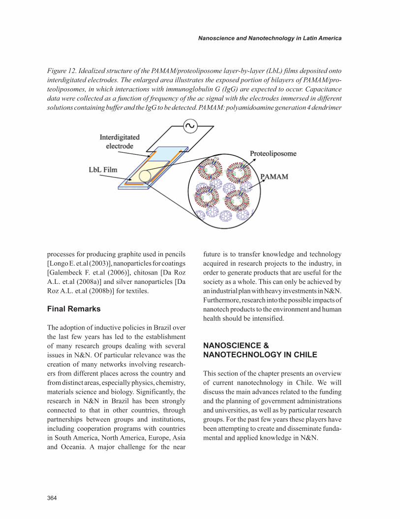
Following the seminal work of [Riul et.al (2002)], a number of developments have been made. For instance, the global selectivity paradigm exploited in typical electronic tongues was ex-tended by employing sensing units with materials capable of molecular recognition toward specific analytes, thus imparting selectivity to biosensors. This was performed with the adsorption of anti-gens on nanostructured films, in an architecture depicted in Figure 12 [Zucolotto et.al. (2007)], with the final sensor array allowing the detection
of antibodies associated with a zoonosis. The latter development holds great promise for clinical di-agnosis. Furthermore, the electrical measurements of an electronic tongue can be correlated with the evaluation of professional tasters in an artificial intelligent system, which allows for inferences to be made about the quality of the beverage under study [Ferreira E.J. et.al (2007)].
In terms of technology resulting from the area of N&N, as indicated by the number of patents–ei-ther deposited or pending-the Brazilian contribu-tion is modest. This has been a stumbling block in the industrial development of the country, as the relatively intense research activity, among the most intense in developing countries, is not matched by generation of technological innovations. Spe-cifically for N&N, the difficulty in transferring technology appears to apply to other countries as well [Zanetti –Ramos B.G. et.al (2008)]. Never-theless, successful initiatives in innovation have been reported, including the development of new
Figure 11. Picture of 5 electronic tongues immersed into different solutions. Reproduced with permis-sion from the PhD thesis of Flávio Pandur Albuquerque Cabral, “Desenvolvimento de instrumentação para uso em língua eletrônica”, Instituto de Física de São Carlos, Universidade de São Paulo, campus of São Carlos
364
Nanoscience and Nanotechnology in Latin America
processes for producing graphite used in pencils [Longo E. et.al (2003)], nanoparticles for coatings [Galembeck F. et.al (2006)], chitosan [Da Roz A.L. et.al (2008a)] and silver nanoparticles [Da Roz A.L. et.al (2008b)] for textiles.
final remarks
The adoption of inductive policies in Brazil over the last few years has led to the establishment of many research groups dealing with several issues in N&N. Of particular relevance was the creation of many networks involving research-ers from different places across the country and from distinct areas, especially physics, chemistry, materials science and biology. Significantly, the research in N&N in Brazil has been strongly connected to that in other countries, through partnerships between groups and institutions, including cooperation programs with countries in South America, North America, Europe, Asia and Oceania. A major challenge for the near
future is to transfer knowledge and technology acquired in research projects to the industry, in order to generate products that are useful for the society as a whole. This can only be achieved by an industrial plan with heavy investments in N&N. Furthermore, research into the possible impacts of nanotech products to the environment and human health should be intensified.
nanoscIence & nanotechnoloGy In chIle
This section of the chapter presents an overview of current nanotechnology in Chile. We will discuss the main advances related to the funding and the planning of government administrations and universities, as well as by particular research groups. For the past few years these players have been attempting to create and disseminate funda-mental and applied knowledge in N&N.
Figure 12. Idealized structure of the PAMAM/proteoliposome layer-by-layer (LbL) films deposited onto interdigitated electrodes. The enlarged area illustrates the exposed portion of bilayers of PAMAM/pro-teoliposomes, in which interactions with immunoglobulin G (IgG) are expected to occur. Capacitance data were collected as a function of frequency of the ac signal with the electrodes immersed in different solutions containing buffer and the IgG to be detected. PAMAM: polyamidoamine generation 4 dendrimer

365
Nanoscience and Nanotechnology in Latin America
Institutions, national Programs, and centers
Since 1967, the principal public agency for the de-velopment of science and technology in Chile has been the National Commission for Scientific and Technological Research, CONICYT. This agency is an autonomous public institution that encour-ages the formation of advanced human resources and the growth and strengthening of research and development in the country-the agency also takes regional development and international linkages into account. CONICYT is able to accomplish its goals mainly through the managing of competitive funds in a series of programs: the National Fund for Scientific and Technological Development (FONDECYT), the Fund for the Advancement of Scientific and Technological Development (FONDEF), the Centers of Excellence in Research Fund (FONDAP), the Non-Formal Science and Technology Education Program (EXPLORA) and, the most recent, the Regional Centers of Science and Technology Development, the Bicentennial Program of Science and Technology (PBCT), and the Basal Financing Program for Scientific and Technological Centers of Excellence (PFB).
During the last few years, two important new initiatives have substantially strengthened the CONICYT, leading to a much improved National Science, Technology and Innovation System. They are, a) The Millennium Science Initiative (MSI) --created under the auspices of the Chilean Min-istry of Planning (MIDEPLAN) to finance the creation and development of the Millennium Centers of Research-- and b) the National Council for the Innovation for Competitiveness (CNIC), which, besides establishing the national policy in science, technology and innovation, has created the Innovation for Competitiveness Fund (FIC) managed by the Chilean Ministry of Economy. These two initiatives together with FONDECYT and the Universities (see below) are expected to play a key role in the present and future of nano-technology in the country.
Indeed, most productivity concerning nano-technology, as measured by the publication of articles in international journals analyzed in the following sub-section, has been at least partially funded by FONDECYT. Although the budget available for this program is relatively modest, generally enough only for individual researchers or small research groups, the productivity in this area has steadily been growing. The efforts made over the last ten years have succeeded enough in regards to the amount of scientific productivity and formation of qualified human resources to make this discipline competitive in the programs offered by the new initiatives commented in the paragraph above. Considering that such programs provide more resources but simultaneously re-quire the increasing of associative research, the productivity rate in N&N is expected to rise, as is the technological innovation and the social impact of the discipline. During the last years a couple of proposals, presented by groups of se-nior researchers and/or labs directly or indirectly interested in nanotechnology, have been financed thus permitting the creation of the following scientific entities:
• The MSI Scientific Nucleus for Basic and Applied Magnetism constituted by research groups of the Universidad de Santiago (USACH), Pontificia Universidad Católica de Chile (PUC), Universidad Técnica Federico Santa María (UTFSM), and Universidad de Chile (UCH), focused on theoretical and experimental studies of magnetism in different nanostructured systems.
• The Center for Nanosciences of Valparaíso gathers scientists from the Universidad Técnica Federico Santa María (UTFSM), the Universidad Católica del Norte (UCN), Pontificia Universidad Católica de Valparaíso (PUCV) and Universidad de Concepción (UdeC).

366
Nanoscience and Nanotechnology in Latin America
• The Center for Development of Nanosciences and Nanotechnology (CEDENNA) which congregates an im-portant number of physicists, chemists, bioscientists, and medicine experts from the Universidad de Santiago (USACH), Pontificia Universidad Católica de Chile (PUC), the Universidad de la Frontera (UFRO) and the Universidad de Chile (UCH).
As for the progress of the science-industry link in the PBCT program, a series of three National Workshops have recently been conducted.
• First National Workshop of Nanotechnology, organized by the UTFSM in Viña del Mar in May 2006, was essen-tially aimed at diagnosing the current situ-ation of Nanosciences / Nanotechnology in Chile and, in turn, at establishing viable strategies for the development of the disci-pline with strong links to industry.
• Second National Workshop of Nanotechnology, organized by the univer-sities PUC and USACH in October 2006 in Viña del Mar, aimed at identifying the industries and economic sectors that could potentially incorporate tools, products and processes based on the application of nanotechnology and at promoting the use of nanotechnology in industrial processes relevant to sustainable development of the country.
• Third National Workshop of Nanotechnology: Linking Industry, Science and Technology, organized by the universi-ties UTFSM, USACH, ECH and PUC in April 2008, aimed at discussing and pro-posing a strategy for research to develop and apply nanotechnology in Chile in the next ten years.
Moreover, in May 2009, the First National Congress on Nanotechnology took place and over 100 individual technical papers were presented.
scientific Productivity
The generation of knowledge in nanotechnology in Chile may be illustrated by the scientific pub-lications in journals indexed by ISI written during the past 10 years, which is shown in Figure 13. This productivity almost entirely corresponds to research done in the context of academic programs at Chilean universities; therefore, it mostly con-cerns basic research. However in the last years the interest in studies related to technological develop-ments and applications has grown. Though there is still no significant activity in the registering of patentable nanotechnology findings there has been some and this is an encouraging response to such efforts. Since the 1980’s the number of universities in Chile has been increasing rapidly, but scientific production stems almost exclusively from labs at traditional institutions. Nevertheless, some of the new private universities have begun to show interesting research activity. The insti-tutional distribution of research productivity in nanotechnology can be appreciated in Figure 14. In the figure., the entry “others” is considered the contributions of Universidad Austral, Universidad Católica del Norte, Universidad de Antofagasta, Universidad Nacional Andrés Bello, Universidad de Valparaíso and Universidad Diego Portales. About fifty percent of the work in nanotechnol-ogy is carried out in Santiago, the capital of the country, because of the geographical concentration of the population, and the scientific infrastructure and facilities. However, recent initiatives like the program PBCT of CONICYT are trying to change such an injurious tendency. Thanks to such efforts and new research centers in places like Concepción, Valparaiso and Antofagasta the nanotechnology activity is being increasing in the provinces [Abalos J. et.al. (2006)].

367
Nanoscience and Nanotechnology in Latin America
Figure 13. Scientific articles on N&N published in international journals (ISI, 2000-2009)
Figure 14. Distribution per institution (%) of international publications on N&N (ISI, 2000-2009)

368
Nanoscience and Nanotechnology in Latin America
Chile’s contribution to research in N&N spreads over a wide spectrum of areas. The dis-tribution of Chilean researchers into sub-areas of nanotechnology research, as classified by ISI Web of Knowledge, is shown in Table 3.
In physics a great part of the research concerns theoretical studies that correlate with the historical development of physics in the country. However, the interest in experimental research, particularly in the field of nanotechnology, has been increasing in the past few years. Research groups in the PUC, UCH, UTFSM and UNAB are generating remarkable re-sults in this field (simulations of surfaces, electronic and magnetic properties of carbon nanotubes, quan-tum dots, and magnetic nanostructures) [Allende S. et.al. (2008); Escrig J. et.al. (2008); Leon A. et.al. (2009)]. The availability of appropriate equipment has been the most important variable in changing the outcomes of this discipline in the country. In order to reach the level required for academic research to become an efficient agent for the development of the country, further policies and resources, both public and private, are required to maintain and sig-nificantly improve the park’s antiquated equipment [Brunner J. (2001)].
In chemistry there are several research groups distributed in different universities. Some of them have relatively long trajectories, and have attained valuable expertise in areas such as the produc-tion of metal nanoparticles in the Universidad de Concepción (UdeC) [Melendrez M. et.al. (2009); Tello A. et.al. (2008)], the preparation of nanostructures or surfaces of low dimensionality by electrochemical methods in the Universidad Católica de Valparaíso, [Cortes A. et.al (2009); Riveros G. et.al. (2008)] and the study of hybrid semiconductor nanocomposites in the Universidad de Chile [O’Dwyer C. et.al (2008); O’Dwyer C. et.al (2006)].
In spite of the fact that bioscience and more recently biotechnology are disciplines which have attained an interesting development, research con-cerning the use of nanotechnology in these fields is only incipient. Nevertheless, some interesting investigations on the use of nanoparticles as ve-hicles of peptides important for the treatment of Alzheimer’s disease are being undertaken in the Universidad de Chile [Kogan M. et.al (2007); Kogan M. et.al (2006)].
The proposal of the recently formed Center CEDENNA--which has joined physicists and chemists with experience in nanotechnology with medical doctors and biologists to help them apply nanotechnology to advance the treatment of medi-cal and veterinary problems--opens a promising window for integrating nanotechnology into the biosciences.
Due to the rather sophisticated and expensive equipment and installations which are necessary for research in nanotechnology, the productiv-ity which has been attained in this area is com-paratively high considering the population and development degree of the country (about 35 international publications per million habitants). This has solely been possible thanks to an active interaction with research groups abroad. The distribution per country of these collaborations is illustrated in Figure 15.
Table 3. Distribution per research sub-area (%) of international articles on nanotechnology (ISI, 2000-2009)
Sub-area/s of nanotechnologyresearch
Percentage(%)
physics, condensed matter 21.54
materials science 21.34
physics, applied 14.03
chemistry, multidisciplinary 13.04
chemistry, physical 11.07
pure nanoscience & nanotechnology 8.50
polymer science 6.52
electrochemistry 4.35
physics, multidisciplinary 4.35
biochemistry & molecular biology 3.75

369
Nanoscience and Nanotechnology in Latin America
funding
In Chile, as frequently occurs in developing counties, the capacity for producing scientific and technological knowledge is mostly concentrated in the universities. This knowledge is centered primordially on basic research, and is generally financed directly by public resources and/or by competitive funds, as well as by external resources from the productive sector and from abroad. In-deed, within the national budget for Research and Development (R&D), about 50% is accorded to the universities. Furthermore, an important part of the research costs are provided by the universi-ties themselves in the form of infrastructure and salaries [Abalos J. et.al. (2006)].
The role of the industrial sector in the creation of science and technology is scarce. Nevertheless both private and autonomous public companies contribute significantly to finance expenses in the R&D in the country. In 2004, the contribu-tion amounted to approximately 45%. Such a role--which though important is still considerably less than companies’ roles in more developed countries--is expected to increase significantly in the near future because of recent R&D pub-
lic policies. Indeed, the recent creation of new Research Centers and Institutes means that the aforementioned governmental initiatives have the mandatory mission of linking academic research to technological innovation, the initiatives must also begin involving the industrial sector (Leipziger D. et.al. (2004); KAEAX (2009)).
education and outreach
Besides the universities’ scientific dissemination, this activity has mainly and efficiently been under-taken by CONICYT through the national program EXPLORA. The objective of this program is to contribute to the creation of a scientific-techno-logical culture for children through non-formal education. The idea is that the children develop an understanding for the benefits of these disciplines, specifically in the area of nanotechnology. Since 2007 we have been conducting a series of talks that were included in the National Week of Science and Technology with the aim of introducing the general public to basic concepts and applications of this new area of knowledge.
Moreover, the universities have implemented lectures and experimental courses to introduce stu-
Figure 15. Distribution per country (%) of international collaborations (articles ISI, 2000-2009)

370
Nanoscience and Nanotechnology in Latin America
dents at different levels of their educational process to basic concepts of nanoscience, nanotechnology and its applications. Often these institutions also offer special activities to train teachers.
final remarks
The synopsis of the state of nanotechnology in Chile described shows that there are about 25 research groups, distributed in the most important universities of the country, which are active in producing knowledge at an international level in this field. Their research has mainly been financed by the universities, by competitive public funds, and is often achieved in collaboration with labs abroad. It is evident that until now this discipline responds more to individual initiatives than to programs specifically designed for the develop-ment of this area. However, new governmental programs and funding instruments --which while aiming to foment associative research have led to the creation of research entities like the Center for Development of Nanosciences and Nano-technology, linking basic research, innovative applications as well as technology to the industrial sector-- are promising and could develop nano-technology more efficiently thereby increasing the social impact of nanoscience and nanotechnology in the near future.
nanoscIence and nanotechnoloGy In mexIco
Nanotechnology is considered the next techno-logical revolution impacting several disciplines, namely information and communication technol-ogy, energy, medicine, genetics, environment and various other fields as it starts moving from the laboratories to new markets. It produces and helps to improve products and production processes with better characteristics or new functionalities. In coming years, products based on nanotechnology are expected to affect nearly all-industrial sectors
and will enter the consumer markets. Considering the future prospects of nanotechnology, countries across the world are investing strongly in this sec-tor. The United States, Japan and Germany alone provide ~52% (12,400 M USD) of the total invest-ment around the world, from this 51% is provided by the governments. Underdeveloped countries have also joined this trend as an alternative to economical growth and global competitiveness. However, this emerging field requires expensive infrastructure to be competitive and special strategies to optimize economical resources are required. Countries leading nanotechnology have implemented initiatives or special programs sup-ported by their corresponding governments.
In Mexico, the Programa Especial de Ciencia y Tecnología (PECyT) 2001-2006, a Mexican gov-ernment program led by the National Council of Science and Technology (CONACyT), considers Nanotechnology as a category within Advanced Materials, which is seen as an emerging, strategic area. The main areas of interest of the program are: catalysis, polymers, nanostructured materials, thin films, semiconductors, metallurgy, biomaterials, optical materials and ceramic advanced materials. It is also mentioned the possibility of implement-ing a Nanotechnology National Program and a Nanotechnology Network to promote scientific exchange. However, no special programs were implemented in this period. CONACyT reported a federal investment of ~$ 1.4 M USD supporting 152 proposals on Nanotechnology involving 58 institutions within the period of 1998-2004. 53% of such investments were in the area of materials, 14% in Chemistry, 14% in Electronics, 12% in Physics and 7% in others (see http://www.nanored.org.mx/documentos.aspx).
At the end of 2006, CONACyT launched two initiatives, the first one focused on constructing National Laboratories and the second one focused on mega proposals or large projects in strategic areas. In the first case, two nanotechnology propos-als were supported with approximately $2 M USD each. In the second case, five pre-proposals were

371
Nanoscience and Nanotechnology in Latin America
supported with approximately $10 K USD each, this money was to be used to prepare and draft the proposal. However, no specific allocations for nanotechnology were made during this period.
In the PECyTI 2007-2012 Nanotechnology, Mechatronics and Biotechnology are considered strategic areas. At the end of 2008, the Nano-technology Network was finally implemented. Its main purpose is to promote the collaboration between scientists and the formation of multidis-ciplinary groups working on projects of national interest. No specific nanotechnology allotments have been launched by the Mexican Government. The situation has now worsened given the current Mexican economic problems. In the absence of a National Initiative on Nanotechnology, Universi-ties and Research Centers have defined their own initiatives--in many cases supported by the local government--and submitted proposals for regular grants from different CONACyt programs. It is important to notice that with CONACyT’s sup-port many centers have signed agreements with foreign Universities.
Here, we describe some of the actions and highlight Nanoscience and Nanotechnology (N&N) contributions from Mexico.
universities and research centers with n&n Programs
According to the Diagnóstico y Perspectivas de la Nanotecnología en México (2008) document, by 2015 more than two million engineers and scientists specialized in nanotechnology will be required worldwide. The document explains that there are 56 Mexican institutions with activities in research and/or education that encompass N&N. There are 12 Undergraduate Programs, 44 Masters in Science Programs, and 43 PhD Programs related to N&N. From those programs, there are 257 PhD and 216 MSc students. There are 450 researchers, 29% are assigned to 14 Centers by the CONA-CyT system, 18% to the National University of Mexico (UNAM), 15% to the Petroleum Mexican
Institute (IMP), 8% to the National Polytechnic Institute (IPN), and 30% are distributed among 20 different institutions.
The UNAM, the largest University in Mexico, concentrates an enormous amount of activity in this emerging field with the leading number of researchers and students working on N&N as-sociated to different Centers and Institutes--in particular, the Center for Nanoscience and Nano-technology (CN&N). This University has some of the best qualifications to perform research on N&N, it is running one the most ambitious projects (PUNTA) related to nanocatalysis for environment with an investment of $1 M USD per year. The IMP depends on the minister of economy and has the most complete capabilities for research on nanocatalysis. Looking at the CONACyT sys-tem, perhaps the centers with the stronger N&N programs are: i) the Advanced Materials Research Center (CIMAV), which focuses on nanomaterials with applications in manufacturing, catalysis and energy. ii) The Applied Chemistry Research Center (CIQA), which focuses in molecular, polymer and magnetic nanomaterials. iii) The Potosino Institute of Scientific and Technological Research (IPICyT), which focuses on carbon and magnetic nanostructure. iv)The Optical Research Center (CIO), which has the Nanophotonic initiatives, focusing on optical properties of nanomaterials for applications in lighting, biomedicine, solar cells and optoelectronic devices. v) The Astrophys-ics, Optics and Electronics Institute (INAOE), which has the nanoelectronic initiative. Many other Universities and Centers are implementing programs in education and research on N&N. However, most of them have limited capabilities to perform this kind of research.
national laboratories
The purpose of creating National Laboratories was to provide the required infrastructure to promote the research of Nanoscience and Nanotechnology. The laboratories should provide accessibility to

372
Nanoscience and Nanotechnology in Latin America
Universities, Institutes and Research Centers in the country, and promote the scientist’s col-laborative efforts to establish multidisciplinary groups. There are three National Laboratories; all of them are part of the CONACyT system. The Nanotechnology National Laboratory (NANO-TECH) (http://nanotech.cimav.edu.mx/) located at CIMAV in the north of Mexico, was created in 2006 and funded by the Mexican Government ($2 M USD). The main activities are focused on the synthesis and characterization of nano-materials, supporting training for undergraduate and graduate programs. The laboratory provides the infrastructure for structural characterization including High Resolution Electron Microscopy with a resolution of 0.1 nm in STEM mode and X-ray diffraction.
The Laboratory for Research in Nanoscience and Nanotechnology (LINAN) (http://materials.ipicyt.edu.mx/LINAN/) located at IPICyT in Cen-tral Mexico was also created in 2006 and funded by the Mexican Government ($2 M USD). The main activities are focused on the synthesis of nanostructures and nanomaterials, nanobiotech-nology, nanocomposites, magnetic nanomaterials, theoretical calculation of electronic properties from nanostructures, and supporting undergraduate and graduate programs. The laboratory provides the infrastructure for structural characterization includ-ing High Resolution Electron Microscopy, X-ray diffraction, Raman spectroscopy, and sputtering.
The Nanoelectronic National Laboratory (LNN) (http://www-elec.inaoep.mx/lnn/index.php) located at INAOE in South Mexico was cre-ated in 2007 funded by the ministry of economy ($ 1.5 M USD), the State of Puebla ($0.5 M USD), and a donation from MOTOROLA of a complete system for the fabrication of integrated circuits and devices. The main activities are focused on the design and fabrication of devices, integrated circuits and MENS, integrating nanomaterials. The laboratory provides the required infrastructure for those purposes, including clean rooms class 10 and 100.
There are many other National Laboratories where nano-scientists from various disciplines collaborate, just to mention a few: the Genomic National Laboratory where biologists and physi-cists are using nanomaterials for DNA sequencing, and the National Center of Metrology, which is implementing the protocols to standardize the measurement of nanomaterials’ physical char-acteristics.
networks and meetings on nanotechnology
As a result of PECyTI 2007-2012, CONACyT has promoted the creation of Networks of Scientists across different fields. Four of the pre-proposals supported at the end of 2006 were joined to become the Network of Nanoscience and Nano-technology (NNN) (http://www.nanored.org.mx/). This network was formally created at the end of 2008. The purpose of this network is foster the development of nanotechnology and integrate scientists from different institutes with a common interest in this emerging field. The formation of multidisciplinary groups or small networks can be expected to resolve problems of national interest in the near future. Already, many scientists from all around the country have joined NNN.
Created in early 2009, the Nanotechnology Network of the State of Guanajuato (RENAG) joined more than 50 scientists from 13 Universi-ties, Institutes and Research Centers. It was funded by CONCYTEG, the Council of Science of the State of Guanajuato, which also supported three proposals that involve collaboration between different groups.
Some Universities have also created internal net-works. UNAM has created REGINA (http://www.fisica.unam.mx/nanoifunam/index.htm) since 2003 integrating more than 60 scientists from different institutes and research centers. It launched the Multidisciplinary Research Program (IMPULSA) integrating more than 100 scientists and graduate students from 13 different centers. The UAM has

373
Nanoscience and Nanotechnology in Latin America
created NanoscienceUAM Network (http://www.nanocienciasuam.com.mx/). The IPN has created the Nanoscience and Micro-Nanotechnology Net-work. The University of Puebla (BUAP) promotes the International Network of Nanoscience and Nanotechnology. The IPICyT is leading the agree-ment between CONACyT and the European Union through NANOFORUMEULA an instrument that creates networks for scientists from México and the European Union as part of the seven-framework program. This initiative promotes the formation of consortiums to resolve problems of common interest by using nanotechnology. An interesting initiative has been launched in the State of Nuevo León where the Research and Technology Innova-tion (PIIT) (http://www.piit.com.mx/?p=acercade) Park has been placed. Located in this place are twelve research centers, seven companies and two business incubators. The areas of interest are Nanotechnology, Health, Mechatronic, Biotechnol-ogy and Information Technology.
There are several periodical conferences focused on Nanoscience and Nanotechnology with the aim to provide a forum for researchers and engineers that bring together scientists work-ing on N&N. The oldest event is the symposia Nanostructured Materials and Nanotechnology on the International Materials Research Congress organized by the Mexican MRS. The International Topical Meeting on Nanostructured Materials and Nanotechnology (NANOTECH) started in 2004 and has been organized by CIO, this year will be the 6th edition. The Mexican Workshop organized by the University of Puebla started in 2005. The Workshop on Metastable and Nanostructured Materials started in 2006 and was organized by IPN. The symposium on Nanoscience and Nanotechnology was organized in 2006 by the Nanoscience Division of the Mexican Physics Society. The NANOMEX meetings are organized by UNAM, and this year is the second edition.
scientific Productivity
As was discussed above, there is strong activity in the Mexican scientific community even in the absence of special federal programs for the devel-opment of N&N. The impact can be estimated by quantifying the scientific production. To quantify the effects, the ISI Web of Science was used with the key word “nano*” as the topic and “Mexico” as the address. A total of 4317 published papers in peer-reviewed scientific journals produced about 37980 citations since 1990 to August 25th 2009, with 82% of total publications published in the last ten years. Figure 16 shows the publication and citations per year. It was observed that there was an increment of 27% in publications and 17% in citations in the last ten years, but the growth has been stronger in the last five. A rough analysis suggests an average publication of 9.6 per scientist, citation per item of 8.8, and an h-index of 72 as a country. The top ten areas of research according to the total publications and considering only those with more than 100 inputs are Chemistry and Chemical Engineering (32%), Materials science (27.3%), Physics & Applied Physics (21.6%), Condensed Matter (18.7%), Atomic & Molecu-lar Physics (6.3%), Optics (4.37%), Electrical & Electronic Engineering (3.72%), Coatings & Films (3.7%), Biochemistry & Molecular Biology (3%), Polymer Science (3%).
Table 4 shows the top twenty more prolific institutions. As expected, 42% of total published papers were produced by the biggest University with the largest budget. The University integrates the largest group of scientists working together via internal networks such as REGINA and PUNTA. The latter launched the most ambitious project on nanocatalysis. The other publications are from the 14 Research Centers directly sup-ported by CONACyT. As was mentioned above, there are nine scientists on average per institution.

374
Nanoscience and Nanotechnology in Latin America
However, the institutions work independently with intermittent collaboration. There is not a network or program to coordinate the efforts of each center and only three of them have received special budgets to support the National Labora-tories. Only six of these centers appear in the top twenty, three of them contribute with more than 2% each in the total published papers. The CIO is the only one with an initiative in optical proper-ties of nanomaterials (NANOPHOTONICS) and contributes with 47% of total published papers in the area of optics. These two examples show the importance of scientists with a common interest working together around one specific problem.
companies
According to the document, Diagnóstico y Per-spectivas de la Nanotecnología en México (2008), there are no Mexican companies producing nanomaterials or nanostructures or nanosystems for new applications or new devices. Most of the companies are interested in nanotechnology, in particular nanomaterials, to improve properties of
materials used for packaging or to design different components. There are very few Mexican compa-nies that do this but these are just commercializing products from other countries. This is reflected in the absence of patents from Mexican institutions, very few applications (either in absolute term or in terms of patents per million inhabitants) from Mexican institutions have been presented to the Mexican Intellectual Property Institute (IMPI). This should be contrasted against other countries, where the number of patents is quite high in this emerging field. More than 1142 registered patents in México are from foreign countries. Such results highlight the urgency of special programs to promote the interaction between companies and research in-stitutions, and proposals focused to solve specific problems with a well-defined market.
final remarks
N&N is believed to be the next industrial revolu-tion and many countries have defined strategies, policies and are investing in this emerging field. Mexico’s interest has been highlighted in the
Figure 16. Published papers and citation per year from 1990 to 29th August 2009. Analysis was performed considering the string, TS=((nano* OR quatum dot* OR quantum wire* OR nanotube* OR carbontub* OR carbon tub* OR buckyball* OR buckyb* OR fullerene* OR self assambled* OR monolayer* OR sers* OR molecular beam epitaxy* OR MBE OR atomic force microscope OR STM OR submicron* OR langmuir blodgett OR plasmonic* OR metamaterials* OR single molecul*) NOT (nanosecond* OR nanogram* OR nanokelvin* OR nanoliter* OR nanovalent*)) AND AD=mexico NOT AD=new mexico, using the Science Citation Index Expanded of the Isi Web of Science

375
Nanoscience and Nanotechnology in Latin America
PECyT 2001-2006 and 2007-2012. However, it has not implemented specific N&N programs. Nevertheless, the N&N activity has been ample as can be seen from the high number of publications and citations. The lack of federal policies, of an entity to manage N&N programs and to invest in this emerging field has been substituted by various efforts either regional or by individual institutions. This deficiency hinders capital investments, the generation of human resources and building the required instrumental capacity. It is imperative to define, fund and implement federal N&N policies, perhaps selecting certain market niches (such as medical applications of nanobiotech) to attain global impact according to the country potential and exploit the opportunity working with all, lo-cal, regional and global partners.
conclusIon
Nanoscience and nanotechnology is already impacting the economy of developed nations and holds an enormous promise to revolutionize existing markets and open new ones. Thus, all developed nations and fast growing countries that leverage the knowledge economy (China, India, Australia, Singapore, Israel, etc.) have launched national efforts to build nano expertise engaging governments, industry, academia, and investing communities. N&N requires collaboration across disciplines, between academia and industry, within countries and regions, and globally. In the knowl-edge economy, the wealth of nations consists of its people (knowledge workers). In the 21st century a country is not competitive if it does not build a
Table 4. Top twenty more prolific Mexican institutions in N&N, from 1990 to 25th August 2009
Institution Published papers
% of 4317 papers
1 National University of Mexico (UNAM) 1786 41.37
2 National Polytechnic Institute (IPN) 669 15.48
3 Metropolitan University (UAM) 285 6.58
4 Petroleum Mexican Institute (IMP) 274 6.34
5 University of San Luis Potosi (UASLP) 268 6.20
6 Benemerita University of Puebla (BUAP) 209 4.83
7 Advanced Research Center (CINVESTAV) 207 4.79
8 Potosino Institute of Scientific and Technological Research (IPICyT)* 176 4.06
9 Advanced Materials Research Center (CIMAV)* 105 2.43
10 University of Sonora (USON) 104 2.41
11 Optical Research Center (CIO)* 89 2.06
12 University of Nuevo León (UANL) 87 2.01
13 University of Morelos State (UAEM) 85 1.97
14 Nuclear Engineering National Institute (ININ) 84 1.94
15 University of Guanajuato (U.de Gto.) 72 1.66
16 Applied Chemistry Research Center (CIQA)* 69 1.58
17 University of Guadalajara (U. de G.) 66 1.52
18 University of Michoacan (UMSNH) 53 1.22
19 Scientific Research Center of Ensenada (CICESE)* 36 0.83
20 National Institute of Astrophysics, Optics and Electronics (INAOE)* 33 0.76
* Centers supported directly by CONACyT.

376
Nanoscience and Nanotechnology in Latin America
strong science and technology infrastructure that produce first class results and is able to bring some of the generated knowledge to the global market, via technology commercialization, new ventures, etc. Complementarily, a country needs to build a competitive, agile workforce that can work in the industries that are dramatically changing at fast pace. So far, Latin America shows a mixed record.
Latin America counts with some strong re-search centers and with a tradition of research ex-cellence in certain disciplines such as medicine and biology, agrobio, nuclear technology, metallurgy and materials among others. The multidisciplinary nature of N&N provides a strong opportunity for building in the region, say, nanobio and nano agro-bio global expertise. In fact, we find that all countries in LA have developed network of researchers across disciplines, centers, etc. within a country, and linking 2 or more countries in the region (e.g., Argentina-Brazil Bi-National Center for Nanoscience & Nanotechnology, CABN). Ad-ditionally, collaborations have extended beyond LA, mainly to USA and the EU. In general, these collaborative programs have already been quite successful in the generation of interdisciplinary N&N research.
Brazil and Argentina have ministries of science and technology, and in both cases they have played key roles in building a national N&N strategy, and in supporting and funding their N&N efforts. In Mexico and Chile the coordinating role has been mainly played by their respective national research council agencies. All these countries have created interdisciplinary national labs, but still in most countries R&D facilities are not well equipped, and researchers are handicapped to leverage their potential for producing high-impact results in N&N. Brazil, in general, counts with the most and better equipped facilities, and the largest funding.
The relation between academia and industry has been improving in the last years, but it is still quite weak. In particular funding incentives for N&N efforts have encouraged joint efforts and con-tributed to catalyze these collaborations. Centers
of excellence that merge academic and industrial sectors, such as the CIDIDI (Argentina), CEITEC (Brazil), Center for Development of Nanosciences and Nanotechnology (Chile), are indeed required for producing high impact research, promote the knowledge transfer and generate innovations. There are some large companies such as Petro-bras (Brazil) with active programs of engagement with academia, or Tenaris (Argentina) which has a solid N&N R&D group that already generated successful nano products for the global market.
A major challenge for the near future is the transformation of knowledge into value, by attracting R&D centers of leading global companies, licensing technologies generated in LA, building new ventures leveraging LA inventions, etc. There are already some suc-cess stories of researchers from LA centers that created new ventures to conquest global markets. For example, a team from INAOE, in Puebla, Mexico, led by Prof. Miguel Arias formed Prefixa Inc. Prefixa started 3 years ago and raised initial funds from CONACYT and other sources in Mexico as it was developing its technology and initial products. Additionally it was assisted by the TechBA accelerator–a program from the Mexican government that helps high-potential companies from Mexico to become global. Prefixa has built a solid patent portfolio, validated its technology and products in the US, and later received funding from an US corporate investor which is also a strategic customer & partner. Prefixa, sells subsystems and licenses technology for optical inspection equipment for the semiconductor industry. Prefixa’s R&D team, based in Puebla, includes several Ph.D.s, that graduated from Miguel’s and other groups at INAOE. From its Silicon Valley office, Prefixa runs its marketing, sales and business development operations working with local (Silicon Valley) experts from the semiconductor industry. To reach US customers and to build the US team, Prefixa leveraged the diaspora of LA professionals in Silicon Valley.

377
Nanoscience and Nanotechnology in Latin America
The diasporas of professionals in Silicon Valley, in US, in EU, etc. have played key roles in the development of the software industry of India, the manufacturing industry of China, the semiconductor industry of Taiwan and Ireland, etc. [Saxenian, A. (2006)]. There are large numbers of LA professionals in US and EU in key academic and industrial positions. On the other hand, LA has only taken very limited advantage of this valuable resource. LatIPnet is a not-for-profit organization, with offices in USA (Silicon Valley), Mexico, Argentina and Spain, that leverages the business potential of the Latin diaspora networks of professionals building win-win partnerships. LatIPnet team has a strong experience in establish-ing industry-academia partnerships, identifying and protecting intellectual property, commercial-izing technology, and building teams and working with investors for establishing new ventures for the global market. LatIPnet assists researchers in understanding the global market potential of their inventions and defining a commercialization strategy, assists institutions and governments on strategies for leveraging the value of knowledge they generate with global approach for build-ing local wealth, and it has already contributed to the creation and launching of several global companies, such as Prefixa, started by academic researchers in Latin America and Spain.
acKnowledGment
This work was partially funded by FAPESP, CNPq and CAPES (Brazil) and by CONCyTEG (Gua-najuato., Mexico). GG likes to thank the Basal Fi-nancing Program for Scientific and Technological Centers of Excellence, CONICYT (CEDENNA), and the FONDECYT (Grant 109 0282), and LB thanks the FONDECYT for postdoctoral fellow-ship (grant 3100088).FA acknowledges Ministry of Science, Technology and Productive Innovation of Argentina, Dr. D. Comedi, Dr. M. Tirado, Dr. E. Calvo and Dr. B. W. de Reca. OO and CC are
grateful to Profs. Oswaldo L. Alves, Cylon Gon-çalves da Silva and Henrique Toma for providing valuable information about N&N initiatives in Bra-zil. AN thanks Bo Varga, Nora Sabelli and Simon Goldbard for enlightening discussions. AN also thanks the Secretaria de Desarrollo Económico Sustentable, Government of Guanajuato for partial support, and local researchers, teachers, business leaders and entrepreneurs for useful discussions on the N&N workforce initiative.
references
Abalos, J., González, L., & Chervellino, M. (2006). Conceptos, antecedentes históricos y actuales de la institucionalidad nacional y sus instrumentos en ciencia, tecnología e innovación . In Las regiones de chile ante la ciencia, tecnología e innovación: diagnósticos regionales y lineamientos para sus estrategias (pp. 24–26). Santiago de Chile, Chile: CONICYT-PBCT.
Abalos, J., González, L., & Chervellino, M. (2006). Diagnóstico y lineamientos estratégicos para el desarrollo de la ciencia, tecnología e innovación en las regiones chilenas . In Las regiones de chile ante la ciencia, tecnología e innovación: diagnósticos regionales y lineamientos para sus estrategias (pp. 262–867). Santiago de Chile, Chile: CONICYT-PBCT.
Allende, J., Babul, J., Martínez, S., & Ureta, T. (2005). Publicaciones y patentes. In
Allende, S., Escrig, J., Altbir, D., Salcedo, E., & Bahiana, M. (2008). Angular dependence of the transverse and vortex modes in magnetic nano-tubes. The European Physical Journal B, 66(1), 37–40. doi:10.1140/epjb/e2008-00385-4
Análisis y proyecciones de la ciencia en Chile (pp. 75-107). Santiago de Chile, Chile: Académia Chilena de Ciencias.

378
Nanoscience and Nanotechnology in Latin America
Argentine Center for Scientific Information and Technology. (2008 January). Nanotechnology: Recent trends and scientific research and tech-nological development. Buenos Aires, Argentina: CAICYT & MINCYT.
Argentine Center for Scientific Information and Technology. (2009 April). Boletin Estadistico Tecnologico, No. 3.
Audebert, F. (2005). Amorphous and Nanostruc-tured Al-Fe and Al-Ni Based Alloys. NATO Science Series II: Mathematics, Physics and Chemistry, 184. Properties and Applications of Nano-crystalline Alloys from Amorphous Precursors (Idzikowski, B., Švec, P., & Miglierini, M., Eds.). Vol. 301). Dordrecht: Kluwer Acad. Publishers.
Audebert, F., Arcondo, B., Rodríguez, D., & Sirkin, H. (2001). Short range order study in. Al-Fe-X melt spun alloys. Journal of Metastable and Nanocrystalline Materials, 10, 155. doi:10.4028/www.scientific.net/JMNM.10.155
Audebert, F., Prima, F., Galano, M., Tomut, M., Warren, P., Stone, I.C., & Cantor, B. (2002). Bulk Amorphous, Nano-Crystalline and Nano-Quasicrystalline Alloys. Special issue materials Transactions JIM, 43-8, 2017.
Babini, N., & De Asua, M. (2003, Vol. 26, N°56). La Historia de la Ciencia en Argentina en el último cuarto de siglo. Revista de la Sociedad Española de Historia de las Ciencias y de las Técnicas, ISSN 0210-8615, 731-738.
Baum, G., Nemirovsky, A., & Sabelli, N. (2008). La Educación en Ciencia y Tecnología como derecho social en la economía del conocimiento. pp. 133-146 in Propuestas interpretativas para una economía basada en el conocimiento. Argentina, Colombia, México, Estados Unidos, Canadá, Fed-erico Stezano y Gabriel Vélez Cuartas, Editors. 1st Ed. January 2008. ISBN 978-84-96571-58-7
Brunner, J. (2001). Factores comunes o trans-versales . In Chile: Informe sobre capacidad tecnológica (pp. 6–13). Santiago de Chile, Chile: Universidad Adolfo Ibáñez.
Caneschi, A., Gatteschi, D., Lalioti, N., Sangre-gorio, C., Sessoli, R., Venturi, G., et al. (2001). Cobalt (II)-nitronyl nitroxide chains as molecular magnetic nanowires. Angewandte Chemie-Inter-national Ed., 40(9), 1760-1763.
Caram, J., Sandoval, C., Tirado, M., Comedi, Cza-ban, J., Thompson, D.A., et al. (2009). Electrical characteristics of core-shell p-n GaAs nanowire structures with Te as the n-dopant. Submitted to Nanotechnology.
Catalog, I. N. N. O. V. A. R. (2007). 3rd Ed. of the National Innovation Competition. Ministry of Science, Technology and Productive Innovation, Argentina.
Catalog, I. N. N. O. V. A. R. (2008). 4rd Ed. of the National Innovation Competition. Ministry of Science, Technology and Productive Innovation, Argentina.
Comedi, D., Tirado, M., Zapata, C., Heluani, S. P., Villafuerte, M., Mohseni, P., et al. (2009). Randomly Oriented ZnO Nanowires Grown on Amorphous SiO2 by Metal-Catalized Vapour Deposition. Submitted to Journal of Alloys and Compounds.
Consejo Nacional de Ciencia y Tecnología México. (2008, December 16). PECyTI 2007-2012. Official periodical. Retrieved from http://74.125.155.132/search?q=cache:9ggPNl8FioMJ:www.siicyt.gob.mx/siicyt/docs/con-tenido/PECYT.pdf+pecyt+2007-2012&cd=2&hl=es&ct=clnk&gl=mx
Consejo Nacional de Investigaciones Cientiíficas y Técnicas Argentina. (2009). II Nanomercosur Meeting: Opportunities for micro- and Nanotech-nology. CONICET’s catalog on Nanoscience & Nanotechnology Institutes.

379
Nanoscience and Nanotechnology in Latin America
CortesA.RiverosG.PalmaJ.DenardinJ.MarottiR.DalchieleE. (2009).
Crespilho, F. N., Pavinatto, F. J., Zucolotto, V., Avansi, W., Barioto, V., Gasparotto, L. H. et al. (2008). Processo de obtenção de um produto a base nanopartículas metálicas e polímeros para tecidos autolimpantes e auto-esterilizantes e produtos resultantes. Patented in Brazil, PI 0.802.649-1.
Da Róz, A. L., Pereiro, L. V., Pavinatto, F. J., Crespilho, F. N., Zucolotto, V., Carvalho, A. J. F., et al. (2008). Produto a base de quitosana e processo de impregnação do mesmo em têxteis. Patented in Brazil, PI 0.802.290-9.
De Reca, W. (2007). Anales de la Academia Na-cional de Ciencias Exactas, Físicas y Naturales. Nanostructured Materials: Synthesis, Character-ization . Properties and Applications, 59, 59–94.
Deheer, W. A., Chatelain, A., & Ugarte, D. (1995). A carbon nanotube field-emission electron. Sci-ence, 270(5239), 1179–1180. doi:10.1126/sci-ence.270.5239.1179
Dresselhaus, M. S., Dresselhaus, G., Jorio, A., Souza, A. G., & Saito, R. (2002). Raman spec-troscopy on isolated single wall carbon nanotubes. Carbon, 40(12), 2043–2061. doi:10.1016/S0008-6223(02)00066-0
Dupont, J., Fonseca, G. S., Umpierre, A. P., Fich-tner, P. F. P., & Teixeira, S. R. (2002). Transition-metal nanoparticles in imidazolium ionic liquids: recycable catalysts for biphasic hydrogenation reactions. Journal of the American Chemical Soci-ety, 124(16), 4228–4229. doi:10.1021/ja025818u
Escrig, J., Lavin, R., Palma, J., Denardin, J., Altbir, D., Cortes, A., et al. (2008). Geometry dependence of coercivity in Ni nanowire arrays. Nanotechnology, 19(7). Retrieved from DOI: 10.1088/0957-4484/19/7/075713.
Ferreira, E. J., Pereira, R. C. T., Delbem, A. C. B., Oliveira, O. N. Jr, & Mattoso, L. H. C. (2007). Random subspace method for analyzing coffee with electronic tongue. Electronics Letters, 43(21), 1138–1140. doi:10.1049/el:20071182
Ferreira, M., Riul, A. Jr, Wohnrath, K., Fonseca, F. J., Oliveira, O. N. Jr, & Mattoso, L. H. C. (2003). High-performance taste sensor made from Langmuir-Blodgett films of conducting polymers and a ruthenium complex. Analytical Chemistry, 75(4), 953–955. doi:10.1021/ac026031p
Galano, M., Audebert, F., García Escorial, A., Stone, I. C., & Cantor, B. (2009). Nanoquasicrys-talline Al-Fe-Cr-based alloys: Part II mechanical properties. Acta Materialia, 57(17), 5120–5130. doi:10.1016/j.actamat.2009.07.009
Galano, M., Audebert, F., Stone, I. C., & Cantor, B. (2008). Effect of Nb on nanoquasicrystalline Al-based alloys. Philosophical Magazine Letters, 88(4), 269. doi:10.1080/09500830801935277
Galano, M., Audebert, F., Stone, I. C., & Cantor, B. (2009). Nanoquasicrystalline Al-Fe-Cr-based alloys: Part I phase transformation process. Acta Materialia, 57(17), 5107–5119. doi:10.1016/j.actamat.2009.07.011
Galembeck, F., & De Brito, J. (2006). Aluminum phosphate or polyphosphate particles for use as pigments in paints and method of making same. U.S. Patent 2006045831.
KAWAX. (2009). Observatorio Chileno de CTI. CONICYT.
Kay, L., & Shapira, P. (2009). Developing nanotechnology in Latin America. Journal of Nanoparticle Research, 11, 259–278. doi:10.1007/s11051-008-9503-z
Kogan, M., Bastus, N., & Amigo, R. (2006). Nanoparticle-mediated local and remote manipu-lation of protein aggregation. Nano Letters, 6(1), 110–115. doi:10.1021/nl0516862

380
Nanoscience and Nanotechnology in Latin America
Kogan, M., Olmedo, I., Hosta, L., Guerrero, A., Cruz, L., & Albericio, F. (2007). Peptides and metallic nanoparticles for biomedical applica-tions. Nanomedicine; Nanotechnology, Biology, and Medicine, 2(3), 287–306.
Leipziger, D., Motta, M., & Dahlman, C. (2004). Chile new economy study (Report No. 25666-CL). In Documents of the World Bank (Vol. 1): Executive Summary and Policy Recommendations (pp. 1-31).
Leon, A., Barticevic, Z., & Pacheco, M. (2009). Coupling and chemical shifts in carbon nano-structures for quantum computing . Chemical Physics Letters, 470(4-6), 249–254. doi:10.1016/j.cplett.2009.01.052
Longo, E., Paskocimas, C. A., Leite, E. R., Mag-nani, R. A., Pontes, F. M. L., & Barroso, V. (2003). Método para transformar carbono amorfo em grafite cristalino em minas de grafite utilizando nanopartículas de metais de transição. Pending patent in Brazil.
Lux. (2008). Nanomaterials State of the Market Q3 2008. Lux Research.
Malsch, I. (2008). Nanotechnology in Argentina. Utrecht, Netherlands: Malsch TechnoValuation.
Meléndrez, D., Motta, M., & Dahlman, C. (2004). Synthesis and aggregation study of tin nanopar-ticles and colloids obtained by chemical liquid deposition. Colloid & Polymer Science, 287(1), 13–22. doi:10.1007/s00396-008-1950-7
Mendoza Zélis, P., Sánchez, M., & Vázquez, J. (2007). Magnetostrictive bimagnetic trilayer rib-bons for temperature sensing. Journal of Applied Physics, 101, 034507. doi:10.1063/1.2422905
Ministry of Education and Science. (2004). PAV Projects Report. SECYT. Argentina: ANPCYT.
Ministry of Education and Science. (2006). Science and Technology Indicators. Argentina: SECYT.
Ministry of Science, Technology and Productive Innovation, Argentina. (2009 April/June). Statistic Bulletin on Technology No. 3.
Nogueira, A. F., Durrant, J. R., & De Paoli, M. A. (2001). Dye-sensitized nanocrystal-line solar cells employing a polymer elec-trolyte. Advanced Materials (Deerfield Beach, Fla.), 13(11), 826. doi:10.1002/1521-4095(200106)13:11<826::AID-ADMA826>3.0.CO;2-L
O’Dwyer, C., Lavayen, V., Fuenzalida, D., Lozano, H., Santa Ana, M., & Benavente, E. (2008). Low-dimensional, hinged bar-code metal oxide layers and free-standing, ordered organic nanostructures from turbostratic vanadium oxide. Small, 4(7), 990–1000. doi:10.1002/smll.200701014
O’Dwyer, C., Navas, D., Lavayen, V., Bena-vente, E., Santa Ana, M., & González, G. (2006). Nano-urchin: The formation and structure of high-density spherical clusters of vanadium ox-ide nanotubes. Chemistry of Materials, 18(13), 3016–3022. doi:10.1021/cm0603809
Poncharal, P., Wang, Z. L., Ugarte, D., & de Heer, W. A. (1999). Electrostatic deflections and elec-tromechanical resonances of carbon nanotubes. Science, 283(5407), 1513–1516. doi:10.1126/science.283.5407.1513
Red de Nanociencias y Nanotecnologioa. (2008). Diagnóstico y Perspectivas de la Nanotecnología en México. Retrieved from http://www.nanored.org.mx/documentos.aspx
Riul, A. Jr, De Sousa, H. C., Malmegrim, R. R., Dos Santos, D. S. Jr, Carvalho, A. C. P. L. F., & Fonseca, F. J. (2004). Wine classification by taste sensors made from ultra-thin films and using neural networks. Sensors and Actuators. B, Chemical, 98(1), 77–82. doi:10.1016/j.snb.2003.09.025

381
Nanoscience and Nanotechnology in Latin America
Riul, A. Jr, Dos Santos, D. S. Jr, Wohnrath, K., Di Tommazo, R., Carvalho, A. C. P. L. F., & Fon-seca, F. J. (2002). Artificial taste sensor: efficient combination of sensors made from Langmuir-Blodgett films of conducting polymers and a ruthenium complex and self-assembled films of an azobenzene-containing polymer. Langmuir, 18(1), 239–245. doi:10.1021/la011017d
Riveros, G., Vasquez, J., Gomez, H., Makarova, T., Silva, D., Marotti, R., & Dalchiele, E. (2008). Single-step electrodeposition of polycrystalline CdSe microwire arrays: structural and optical properties. Applied Physics. A, Materials Sci-ence & Processing, 90(3), 423–430. doi:10.1007/s00339-007-4318-9
Rodrigues, V., Fuhrer, T., & Ugarte, D. (2000). Signature of atomic structure in the quantum conductance of gold nanowires. Physical Review Letters, 85(19), 4124–4127. doi:10.1103/Phys-RevLett.85.4124
Saporiti, F., Boudard, M., & Audebert, F. (2009). Short range order in Al-Fe-Nb, Al-Fe-Ce and Al-Ni-Ce metallic glasses. Submitted to J. Alloys & Compounds.
Saxenian, A. (2006). The New Argonauts: Region-al Advantage in a Global Economy. Cambridge, MA: Harvard University Press.
Schneider, O., & Sanchez, R. (1980). Evolución de las ciencias en la Republica Argentina 1923-1973: Vol. 8. Geofisica y Geodesia. Buenos Aires, Argentina: Sociedad Científica Argentina.
Single-Crystal Growth of Nickel Nanowires.. In-fluence of deposition conditions on structural and magnetic properties. Journal of Nanoscience and Nanotechnology, 9(3), 1992–2000. doi:10.1166/jnn.2009.374
Smith, G. W., Audebert, F., Galano, M., & Grant, P. (n.d.). Metal Matrix Composite Material. Patent Application Ner: PCT/GB2007/004004.
Tello, A., Cardenas, G., Haberle, P., & Segura, R. (2008). The synthesis of hybrid nanostructures of gold nanoparticles and carbon nanotubes and their transformation to solid carbon nano-rods. Carbon, 46(6), 884–889. doi:10.1016/j.carbon.2008.02.024
The National Council of Science and Technology in Mexico. (2006). Programa Especial de Ciencia y Tecnología 2001-2006. Retrieved from http://www.siicyt.gob.mx/siicyt/docs/Programa_Nacio-nal_de_C_y_T_1970-2006/documentos/PECYT.pdf
Toma,H. E.(2008). ‘08 Workshop of the Thematic Net of Petrobras: Research on molecular interfaces applied to oil and gas nanotechnology.
Vago, M., Tagliazucch, M., Williams, F. J., & Cal-vo, E. J. (2008). Electrodeposition of a palladium nanocatalyst by ion confinement in polyelectrolyte multilayers. Chemical Communications, 44, 5746. doi:10.1039/b812181h
Zanetti-Ramos, B. G., & Creczynski-Pasa, T. B. (2008). Nanotechnology development: world-wide and national investments. Rev. Bras. Farm., 89(2), 95–101.
Zheng, M., Jagota, A., Strano, M. S., Santos, A. P., Barone, P., & Chou, S. G. (2003). Structure- based carbon nanotube sorting by sequence-dependent DNA assembly. Science, 302(5650), 1545–1548. doi:10.1126/science.1091911
Zucolotto, V., Daghastanli, K. R. P., Hayasaka, C. O., Riul, A. Jr, Ciancaglini, P., & Oliveira, O. N. Jr. (2007). Using capacitance measurements as the detection method in antigen-containing layer-by-layer films for biosensing. Analytical Chemistry, 79(5), 2163–2167. doi:10.1021/ac0616153
Copyright © 2022 FDOKUMEN