Nanoscale Strainability of Graphene by Laser Shock-Induced Three-Dimensional Shaping
7
Nanoscale Strainability of Graphene by Laser Shock-Induced Three- Dimensional Shaping Ji Li, †,‡ Ting-Fung Chung, †,∥ Yong P. Chen, †,§,∥ and Gary J. Cheng* ,†,‡ † Birck Nanotechnology Center, ‡ School of Industrial Engineering, § School of Electrical and Computer Engineering, and ∥ Department of Physics, Purdue University, West Lafayette, Indiana 47907, United States ABSTRACT: Graphene has many promising physical properties. It has been discovered that local strain in a graphene sheet can alter its conducting properties and transport gaps. It is of great importance to develop scalable strain engineering techniques to control the local strains in graphene and understand the limit of the strains. Here, we present a scalable manufacturing process to generate three-dimensional (3D) nanostructures and thus induce local strains in the graphene sheet. This process utilizes laser-induced shock pressure to generate 3D tunable straining in the graphene sheet. The size dependent straining limit of the graphene and the critical breaking pressure are both studied. It is found that the graphene film can be formed to a circular mold (∼50 nm in diameter) with an aspect ratio of 0.25 and strain of 12%, and the critical breaking pressure is 1.77 GPa. These values were found to be decreasing with the increase of mold size. The local straining and breaking of graphene film are verified by Raman spectra. Large scale processing of the graphene sheet into nanoscale patterns is presented. The process could be scaled up to roll-to-roll process by changing laser beam size and scanning speed. The presented laser shock straining approach is a fast, tunable, and low-cost technique to realize strain engineering of graphene for its applications in nanoelectrical devices. KEYWORDS: Laser shock-induced straining, 3D nano shaping, graphene, strainability G raphene, an atom-thick layer of carbon, has attracted significant attention since its experimental discovery in 2004. 1 As the mother of all graphitic materials such as fullerenes, carbon nanotubes, and graphite, graphene possesses unusual properties, including structural perfection, low density, excellent electrical properties, 2,3 zero effective mass near the Dirac point, 4 long mean free path, 5 and superior mechanical properties. 6 However, unpatterned graphene has limited functionality 4,7 because of its zero bandgap. One approach has been developed which patterns graphene into nanoribbons and dots. 8,9 However, reliability and scalability remain problems for graphene nanopatterning. The high disorder level of the patterned graphene and sensitivity of transport to the edge profile, as well as the difficulty in controllable and repeatable fabrication of such microstructures with sharply defined edges, severely limit the application of graphene nanoribbons in electronics. Recently, more focus has been put on another approach, straining, to tailor the electronic properties of graphene. 10−12 It has been shown that all of the characteristics of graphene ribbons and dots could be obtained by generation of local strain in graphene lattice, which allows one to make an all-graphene circuit. 10 Meanwhile, certain configurations of strains in graphene are equivalent to a magnetic field, which could be very high. 12,13 Thus, it is of great importance to develop scalable manufacturing techniques to precisely induce the amounts and types of strains in graphene films. It has been proposed that this can be achieved by suspending graphene on a substrate with different geometrical patterns, such as grooves, creases, steps, and wells. 10 However, it is difficult to control the strain level in graphene that varies as a result of both transfer processes and operation errors. Here, we present a scalable manufacturing process to precisely induce local strains in the graphene sheet. This process utilizes laser-induced shock pressure to generate three- dimensional (3D) shaping in the graphene sheet. The graphene sheet is conformally pressed onto the mold patterns and takes the shape of the patterns, resulting tunable strains in the graphene sheet. The graphene is attached to the mold surface after the laser shock, due to the van der Waals force. As a result, the 3D strained shapes remain after the process. The strainability of the graphene film is studied by varying the forming depth in order to find out the maximum straining aspect ratio (depth over diameter in the deformed area) as a function of mold diameters. The critical pressure needed to break the graphene film as a function of size of holes is also studied. Raman spectroscopy is used to verify the local straining and breaking of the graphene film. The laser shock-induced graphene straining process is illustrated in Figure 1. The nanopatterns on Si wafer were fabricated by focused ion beam (FIB) milling or e-beam lithography. Chemical vapor deposition (CVD) grown single layer graphene film is transferred on to the Si mold. Laser dynamic forming (LDF) process 14,15 is then carried out on the graphene film, as seen in Figure 1a. When the laser pulse Received: May 15, 2012 Revised: August 2, 2012 Published: August 9, 2012 Letter pubs.acs.org/NanoLett © 2012 American Chemical Society 4577 dx.doi.org/10.1021/nl301817t | Nano Lett. 2012, 12, 4577−4583
Transcript of Nanoscale Strainability of Graphene by Laser Shock-Induced Three-Dimensional Shaping

Nanoscale Strainability of Graphene by Laser Shock-Induced Three-Dimensional ShapingJi Li,†,‡ Ting-Fung Chung,†,∥ Yong P. Chen,†,§,∥ and Gary J. Cheng*,†,‡
†Birck Nanotechnology Center, ‡School of Industrial Engineering, §School of Electrical and Computer Engineering, and ∥Departmentof Physics, Purdue University, West Lafayette, Indiana 47907, United States
ABSTRACT: Graphene has many promising physical properties. It has been discovered thatlocal strain in a graphene sheet can alter its conducting properties and transport gaps. It is ofgreat importance to develop scalable strain engineering techniques to control the local strainsin graphene and understand the limit of the strains. Here, we present a scalablemanufacturing process to generate three-dimensional (3D) nanostructures and thus inducelocal strains in the graphene sheet. This process utilizes laser-induced shock pressure togenerate 3D tunable straining in the graphene sheet. The size dependent straining limit of thegraphene and the critical breaking pressure are both studied. It is found that the graphenefilm can be formed to a circular mold (∼50 nm in diameter) with an aspect ratio of 0.25 andstrain of 12%, and the critical breaking pressure is 1.77 GPa. These values were found to bedecreasing with the increase of mold size. The local straining and breaking of graphene filmare verified by Raman spectra. Large scale processing of the graphene sheet into nanoscalepatterns is presented. The process could be scaled up to roll-to-roll process by changing laserbeam size and scanning speed. The presented laser shock straining approach is a fast, tunable,and low-cost technique to realize strain engineering of graphene for its applications in nanoelectrical devices.
KEYWORDS: Laser shock-induced straining, 3D nano shaping, graphene, strainability
Graphene, an atom-thick layer of carbon, has attractedsignificant attention since its experimental discovery in
2004.1 As the mother of all graphitic materials such asfullerenes, carbon nanotubes, and graphite, graphene possessesunusual properties, including structural perfection, low density,excellent electrical properties,2,3 zero effective mass near theDirac point,4 long mean free path,5 and superior mechanicalproperties.6 However, unpatterned graphene has limitedfunctionality4,7 because of its zero bandgap. One approachhas been developed which patterns graphene into nanoribbonsand dots.8,9 However, reliability and scalability remain problemsfor graphene nanopatterning. The high disorder level of thepatterned graphene and sensitivity of transport to the edgeprofile, as well as the difficulty in controllable and repeatablefabrication of such microstructures with sharply defined edges,severely limit the application of graphene nanoribbons inelectronics. Recently, more focus has been put on anotherapproach, straining, to tailor the electronic properties ofgraphene.10−12 It has been shown that all of the characteristicsof graphene ribbons and dots could be obtained by generationof local strain in graphene lattice, which allows one to make anall-graphene circuit.10 Meanwhile, certain configurations ofstrains in graphene are equivalent to a magnetic field, whichcould be very high.12,13 Thus, it is of great importance todevelop scalable manufacturing techniques to precisely inducethe amounts and types of strains in graphene films. It has beenproposed that this can be achieved by suspending graphene ona substrate with different geometrical patterns, such as grooves,creases, steps, and wells.10 However, it is difficult to control the
strain level in graphene that varies as a result of both transferprocesses and operation errors.Here, we present a scalable manufacturing process to
precisely induce local strains in the graphene sheet. Thisprocess utilizes laser-induced shock pressure to generate three-dimensional (3D) shaping in the graphene sheet. The graphenesheet is conformally pressed onto the mold patterns and takesthe shape of the patterns, resulting tunable strains in thegraphene sheet. The graphene is attached to the mold surfaceafter the laser shock, due to the van der Waals force. As a result,the 3D strained shapes remain after the process. Thestrainability of the graphene film is studied by varying theforming depth in order to find out the maximum strainingaspect ratio (depth over diameter in the deformed area) as afunction of mold diameters. The critical pressure needed tobreak the graphene film as a function of size of holes is alsostudied. Raman spectroscopy is used to verify the local strainingand breaking of the graphene film.The laser shock-induced graphene straining process is
illustrated in Figure 1. The nanopatterns on Si wafer werefabricated by focused ion beam (FIB) milling or e-beamlithography. Chemical vapor deposition (CVD) grown singlelayer graphene film is transferred on to the Si mold. Laserdynamic forming (LDF) process14,15 is then carried out on thegraphene film, as seen in Figure 1a. When the laser pulse
Received: May 15, 2012Revised: August 2, 2012Published: August 9, 2012
Letter
pubs.acs.org/NanoLett
© 2012 American Chemical Society 4577 dx.doi.org/10.1021/nl301817t | Nano Lett. 2012, 12, 4577−4583

transmits through the confinement and irradiates the ablativecoating, it quickly vaporizes and ionizes into plasma. Theexpansion of the plasma is confined and bounced off by theconfining media, generating a strong shock wave, whichprovides a strong momentum to shape the graphene filmonto the mold surface. The thin aluminum foil is positionedbetween ablative coating and graphene film to prevent directcontact of ionized plasma on graphene and also effectivelytransfer the shock pressure onto the graphene sheet. It is been
found that metals experience superplasticity during high strainrate forming, which allows the metal foils deforms into thenanoscale 3D mold. Therefore, after the impact of the laser-ablated shock pressure, the metal foil, and graphene sheet ispressed into the patterned on the mold and firmly attached tothe substrate surface. The duration of the shock is only tens ofnanoseconds, and the process involves one step operation. Inorder to apply uniform pressure on large areas, a beam diffusercould be used to flatten the Gaussian profile of fundamentalmode laser beam. With a motion controlled table or a beamscanner and high pulse frequency, the laser shock-inducedstraining process could used to apply large scale shaping ofgraphenes at high speed.Figure 1b shows the results of laser shock induced shaping
on graphene layer. The FIB slicing view clearly shows thegraphene’s profile before and after shaping. When the shockpressure is lower than a critical value, graphene sheet waselastically strained and conformally attached on the siliconmold by van der Waals force. When the shock pressure is highenough, the graphene sheet experiences breaking around theedges of the mold because its straining limit is exceeded, asshown in Figure 1c. The magnitudes of the strains are tunablebased on the mold geometry. This study will investigate thecritical straining and pressure levels that the graphene film canattain, beyond which breaking of the graphene will take place.The breaking of graphene film has other applications, such aspatterning of graphene;16 however, this study is focused on thestraining range of graphene and the shaping level that could beachieved.More results of laser nanoshaping and straining of graphene
are given in Figure 2. Examples of the original sample withgraphene film lying over nano molds are illustrated in Figure2a,d. Figure 2a shows a typical scanning electron microscopy(SEM) image of the sample on channel mold. The width of the
Figure 1. Illustration of the laser shock induced straining of graphene.(a) Setup of of the laser-induced strain engineering; (b) tunable 3Dnanostraining of the graphene film when the strain limit is notexceeded. (c) Graphene straining above the strain limit.
Figure 2. SEM and AFM images of (a) graphene film transferred to a silicon mold patterned with arrays of channels before laser shock shaping; (b,c)graphene film deformed into channels; (d) graphene film transferred to a silicon mold patterned with circular wells; (e,f) graphene film deformedinto wells. The samples are tilted 52° for SEM observation.
Nano Letters Letter
dx.doi.org/10.1021/nl301817t | Nano Lett. 2012, 12, 4577−45834578
mold is about 30 nm and the depth is about 12 nm. Somepoly(methyl methacrylate) (PMMA) residuals are observed onthe surface of the graphene, which are left over from thePMMA-assisted transfer process of the CVD grown graphenefilm. Morphology of the suspending graphene film on Si moldis observed by atomic force microscopy (AFM). It can be seenthat the surface of the graphene film is very flat with an overallroughness characterized as 3.5 nm. Figure 2d shows the SEMand AFM images of graphene film suspending on circularmolds. Normally graphene film suspending on mold cavitiestends to slightly bend into and thus stretch across the openingsdue to the van der Waals attraction of the membrane to thesubstrate.18 However, the stretching of the graphene film is verysmall in this study due to the small size of the mold and ishardly seen from the height profile information. Therefore, thestretching and prestressing in the graphene film can beneglected.During the laser shock operation, the graphene film is
pressed onto the nanomolds by the strong and short lasershock pressure, resulting in local straining of the film. The lasershock pressure value can be estimated by Fabbro’s model19 inwhich the peak pressure value in confined laser ablation processis given by
αα
=+
⎜ ⎟ ⎜ ⎟⎜ ⎟⎛⎝
⎞⎠
⎛⎝
⎞⎠
⎛⎝
⎞⎠P Z I(GPa) 0.01
2 3g
cm sGWcm
1/21/2
2 01/2
2 (1)
where α is the fraction of absorbed energy (typically equals to0.1), I0 is laser intensity, and Z is calculated by
= +Z Z Z2 1 1
1 2 (2)
where Z1 and Z2 are the impedances of the confining media(glass) and the substrate material (aluminum foil), respectively.As the confining media and the metallic foil are kept the
same in the experiments, the laser shock pressure is controlledby adjusting the laser intensity. The laser intensity used in thisstudy ranges from 0.2 to 0.7 GW/cm2, and the calculated lasershock pressure ranges from 1.0 to 1.8 GPa. The actual pressureapplied on the graphene film is slightly smaller than the lasershock pressure due to the attenuation in the aluminum foil,which is neglected in this study. The laser intensity of 0.2 to 0.7GW/cm2 could be achieved on 3 mm area with pulse energy of70 to 230 mJ and pulse duration of 5 ns for a Gaussian beamprofile. Larger area can be processed using a beam scanner.As shown in both SEM images (sample is tilted 52°) and
AFM images in Figure 2b,c,e,f, after the laser shock shapingprocess, the graphene film is no longer suspending on thenanomolds (channels or holes), but is attaching to the curvedsurface of the Si substrate and nicely takes the shape of themolds. The laser intensity used is 0.45 GW/cm2, correspondingto an estimated pressure of 1.5 GPa. As the graphene film isfixed at the bar positions of the substrate, these parts of the filmhas little change before and after the laser shock operation. Inthe contrast, the freestanding parts of the film originallysuspending on the mold cavities are suddenly hit and pressedby the pressure impact, resulting in local straining of themembrane. The local straining in the graphene layer can becontrolled by varying prefabricated patterns on the substrateand appropriate pressure shock. The AFM characterization alsogives the height profiles of the deformed graphenes. Examplesare shown in Figure 2c,f, which give an average forming depthof 12 nm for the 30 nm wide channel mold, and a depth of 31
nm for the 250 nm diameter circular mold, and the graphenefilm is well shaped without fracture in these two cases.During the deformation process, there is a critical straining
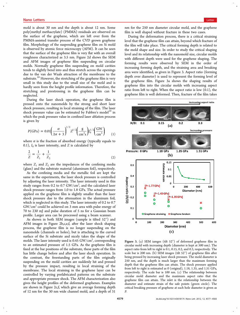
level that the graphene film can attain, beyond which fracture ofthe film will take place. The critical forming depth is related tothe mold shape and size. In order to study the critical shapinglevel and its relationship with the nanomold size, circular moldswith different depth were used for the graphene shaping. Theforming results were observed by SEM in the order ofincreasing forming depth, and the straining area and breakingarea were identified, as given in Figure 3. Aspect ratio (formingdepth over diameter) is used to represent the forming level ofthe graphene film. Figure 3a shows the shaping results ofgraphene film into the circular molds with increasing aspectratio from left to right. When the aspect ratio is low (0.1), thegraphene film is well deformed. Then, fracture of the film takes
Figure 3. (a) SEM iamges (tilt 52°) of deformed graphene film incircular mold with increasing depth (diameter is kept at 500 nm). Theaspect ratio from left to right is 0.1, 0.15, 0.2, and 0.3, respectively. Thescale bar is 200 nm. (b) SEM images (tilt 52°) of graphene film afterbeing pressed by increasing laser shock pressure. The mold diameter is250 nm, and the depth is much larger than the maximum formingdepth that the graphene film can attain. The shock pressure appliedfrom left to right is estimated as 0 (original), 1.18, 1.35, and 1.51 GPa,respectively. The scale bar is 100 nm. (c) The relationship betweencircular mold diameter and the maximum aspect ratio that thegraphene film can attain. The inlet is the relationship between thediameter and estimate strain of the safe points (green circle). Thecritical breaking pressure of graphene at each hole diameter is given asP.
Nano Letters Letter
dx.doi.org/10.1021/nl301817t | Nano Lett. 2012, 12, 4577−45834579

place at the edge of the mold with aspect ratio is increased to0.15, and becomes more severe at a higher aspect ratio of 0.2.The round piece was pulled off at aspect ratio of 0.3. Theexperimental observation agrees well with MD simulationresults of the graphene forming process,16 in which thegraphene film first bulges by the pressure, and then fracturetakes place at the edge and gradually becomes larger with thecontinuous increasing of straining. The deformed part of thefilm is pulled off at the edge. The reason that the fracture occursat the edge of the mold is that the graphene film turns sharplywhile bending into the mold cavity, resulting in severe tensionbetween the carbon atoms and high local strain.The relationship between the mold diameter and critical
aspect ratio is plotted in Figure 3c. Green circles are the highestsafe aspect ratios the graphene film can be deformed to inexperiment, and the area below the green circles is the safeforming area. The aspect ratios at which breaking of graphenewere observed are marked by red crosses in the figure. Thecritical aspect ratio should be located between the red crossesand the green circles. The highest aspect ratio andcorresponding strains reaches 0.25 and 12%, respectively, fora 50 nm circular mold. The maximum aspect ratio the graphenegradually increases with the decreasing of the mold diameter.When the mold diameter is smaller than 100 nm, the increasingrate of the aspect ratio becomes higher. The increasing ofmaximum aspect ratio with decreasing of mold size can beexplained by the level of uniformity of the strain over the entiredeformed area of graphene. The corresponding average strainof the safe aspect ratios (green circles) are plotted in the inlet ofFigure 3a. It can be seen that with the decreasing of the moldsize, the average strain in the deformed graphene beforebreaking increases. When the mold size is relatively large (over
100 nm), the carbon atoms at the edge experienced very highlocal strain while the others close to the center deforms little.Therefore, when the strain at the edge is high enough to causefracture, the overall deformed aspect ratio/strain is still low.With the decreasing of mold size, the amount of carbon atomsin the forming area decreases and the portion of edge atoms arelarger, so the strain across the whole area becomes more andmore uniform, resulting in higher forming aspect ratio. It can bepredicted that in an ideal and extreme case with only severalcarbon atoms being deformed, each C−C bond can beelongated to the theoretical ultimate strain.The study of the maximum aspect ratio is of important
meaning as guidance for carrying out nanostrain engineering ofgraphene in the future. Besides the straining limit, the criticalpressure that the graphene film can sustain is another importantparameter to study. Circular molds with deep depth (deeperthan the maximum aspect ratio that the graphene can attain)are used to study the critical pressure. Increasing laser intensity(shock pressure) is applied on the suspending graphene filmand observed afterward, as seen in Figure 3b. It can be seen thatwhen the pressure is increased to a low value, there is noobvious change in the film. As the hole is deep, although thepressure is enough to deform the graphene film, there is nosurface for the film to attach to and hold its strained shape.Thus, after the release of the force the graphene would bounceback to the unstrained state. Once the exerted pressure is largerthan the critical pressure, the graphene film will be broken. Thecritical pressure is related to the mold diameter in nanoscale,which was given in Figure 3c. It is found that the criticalpressure increases slowly in the diameter range of 100 and 500nm. In order to safely shape the graphene film intocorresponding mold, smaller pressure should be used. The
Figure 4. (a) Schematic of Raman excitation laser beam relative to graphene sample on circular molds. (b−d) Comparison of Raman D, G, and 2Dpeaks on unstrained region, max-strained region, and strained above limit region. The Raman shift is 15 cm−1 after laser straining, as shown in (c)when the circular mold of 250 nm in diameter and 30 nm in depth is used. The Raman shift after breaking occurs is zero, as shown in (d) when themold is 250 nm in diameter and 60 nm in depth.
Nano Letters Letter
dx.doi.org/10.1021/nl301817t | Nano Lett. 2012, 12, 4577−45834580
breaking process of the graphene film is useful for nano-patterning application, and more details can be found in ref 16.The straining of the graphene film are further studied by
Raman spectroscopy. The Raman spectra of unstrainedgraphene, graphene max-strained, and graphene strainedabove limit on circular mold with 250 nm diameter wasmeasured, as plotted in Figure 4b−d. The Raman excitationlaser beam (λ = 532 nm) is about 1 μm and thus is larger thanthe mold diameter and covers an area with several molds, asillustrated by Figure 4a. It can be seen from Figure 4b that theoriginal CVD graphene sample is a typical single layergraphene20−23 with the characteristic features as D, G, and2D peaks, which lie at 1346, 1590, and 2689 cm−1, respectively.The D peak is very small, indicating a good quality of the film.The circular mold used is 250 nm in diameter and 30 nm indepth, corresponding to a forming aspect ratio of 0.12 andaverage strain of 3.8% of the strained area of graphene. Afterthe graphene film is strained to aspect ratio (0.12) in circularmolds in diameter of 250 nm, the G peak downshifts 7 cm−1 to1583 cm−1, and the 2D peak down shifts 15 cm−1 to 2674 cm−1.The Raman frequency shifts verify the forming and straininduced in the graphene membrane.21−23 In addition, besidesdownshift, the G peak of deformed graphene film also showslight broadening on the left part and becomes unsymmetrical.It is a sign of splitting of G peak, which is also a strain effect.21
The Raman spectrum of fractured graphene film is plotted in
Figure 4d, in which the graphene film is deformed into 250 nmwide and 60 nm deep circular mold (aspect ratio = 0.24). Noobvious downshifts of G peak and 2D peak are observed. Thisis because after broken the strain induced in the deformed partof graphene is released. Meanwhile, an obvious increase of Dpeak is seen, indicating an increase of disorder and defect in thetest area, and thus verifies the fracture of the graphene film.The relationship between aspect ratio of mold (D = 250 nm,
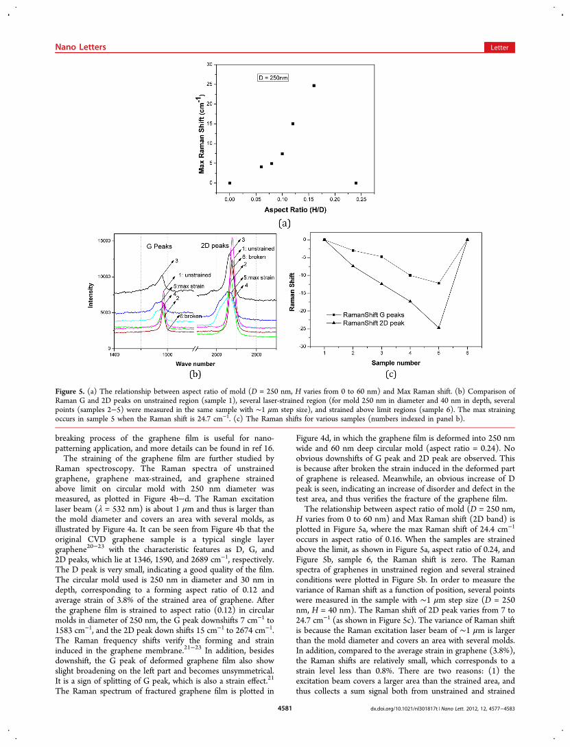
H varies from 0 to 60 nm) and Max Raman shift (2D band) isplotted in Figure 5a, where the max Raman shift of 24.4 cm−1
occurs in aspect ratio of 0.16. When the samples are strainedabove the limit, as shown in Figure 5a, aspect ratio of 0.24, andFigure 5b, sample 6, the Raman shift is zero. The Ramanspectra of graphenes in unstrained region and several strainedconditions were plotted in Figure 5b. In order to measure thevariance of Raman shift as a function of position, several pointswere measured in the sample with ∼1 μm step size (D = 250nm, H = 40 nm). The Raman shift of 2D peak varies from 7 to24.7 cm−1 (as shown in Figure 5c). The variance of Raman shiftis because the Raman excitation laser beam of ∼1 μm is largerthan the mold diameter and covers an area with several molds.In addition, compared to the average strain in graphene (3.8%),the Raman shifts are relatively small, which corresponds to astrain level less than 0.8%. There are two reasons: (1) theexcitation beam covers a larger area than the strained area, andthus collects a sum signal both from unstrained and strained
Figure 5. (a) The relationship between aspect ratio of mold (D = 250 nm, H varies from 0 to 60 nm) and Max Raman shift. (b) Comparison ofRaman G and 2D peaks on unstrained region (sample 1), several laser-strained region (for mold 250 nm in diameter and 40 nm in depth, severalpoints (samples 2−5) were measured in the same sample with ∼1 μm step size), and strained above limit regions (sample 6). The max strainingoccurs in sample 5 when the Raman shift is 24.7 cm−1. (c) The Raman shifts for various samples (numbers indexed in panel b).
Nano Letters Letter
dx.doi.org/10.1021/nl301817t | Nano Lett. 2012, 12, 4577−45834581

parts; and (2) the strain induced in the bent area is notuniform. When pushed into the circular molds, the graphenefilm is heavily strained at the edges of the trenches andshoulders near side walls, where the signal can hardly becollected. Thus, only signals from flat areas of graphene whichare either slightly strained (bottom of shaped area) orunstrained (bar areas without mold cavities) are collected,resulting small shift in Raman spectrum.As the laser beam size used is in millimeter scale, it allows for
scalable treatment of the graphene surface while inducingnanoscale local straining in the graphene film. The positions,numbers, and amounts of local straining are controlled by thesize and shapes of the nanopatterns on the substrate surface.Combining with the existing scalable patterning technique, suchas photolithography, laser interference lithography, and E-beamlithography, the treated area in the proposed laser strainingprocess could be further scaled up to roll to roll or plate to plateprocesses by adjusting the laser beam size and the scanningspeed.In summary, 3D shaping of CVD grown graphene film in
nanoscale patterns using laser shock pressure was carried out,which induces local straining in the graphene film. Thestraining limit of the graphene film and the critical breakingpressure were studied. It is found that the graphene film candeform to an aspect ratio larger than 0.1, and the criticalbreaking pressure is higher than 1 GPa. Both values were foundto increase with the decreasing of mold size. The local strainingand breaking of graphene film are verified by Raman spectra.Large scale pressing of the graphene film into nanoscale localpatterns was presented. The process could be scaled up to rollto roll process by changing laser beam size and scanning speed.The proposed laser shock straining approach is fast, efficient,and easy, which has great potential to realize all graphenecircuit for applications of graphene in nanoelectrical devices.Methods. Setup of Laser Dynamic Forming. The laser
shock process is similar to the one used in laser dynamicforming of thin films. The setup includes a laser source, atransparent confinement, a layer of ablative coating and anultrathin metal foil, as illustrated in Figure 1a). A short pulsedQ-switch Nd:YAG (Continuum Surelite III) is used as theenergy source. The laser beam has a Gaussian distribution andthe pulse width is 10 ns. A focus lens is used to control the bamsize. The beam diameter used is 3 mm, which is calibrated by aphotosensitive paper (Kodak Linagraph, type: 1895). Glassslide was used as the confining media, and aerosol graphitepainting (Asbury Carbons, U.S.A.) was sprayed on 4 μm thickaluminum foil (Lebow Company Inc., Bellevue, WA) as theablative coating. The thickness of the ablative coating is in therange from 1 to 10 μm. An X−Y stage is used to move theprocessing stage.Graphene Synthesis and Transfer. Our graphene samples
are grown by CVD (CH4 as carbon stock) on Cu foils (25 μmthick, Alfa Aesar, 99.8%) at ambient pressure. The Cu foil wasloaded into a CVD furnace and heated to 1050 °C in 460 sccmof flowing 5% H2/Ar. After 1050 °C was attained, the samplewas annealed for at least 30 min without changing the gas flowrates. Then CH4 (concentration 500 ppm) was injected intothe furnace at 50 sccm for 90 min before the system was cooledto room temperature under protection of Ar and H2. After thegrowth process, the graphene samples were transferred by aPMMA-assisted process in a Cu etchant (iron nitrate) ontopatterned Si mold.17
Preparation of Silicon Mold. Two methods are used preparemold by cutting patterns on silicon wafers. The first one isfocused ion beam (FIB) milling performed by FEI Nova 200Nano-Lab DualBeam TM-SEM/FIB. The second method iselectron beam lithography (EBL) using Leica VB-6 ultrahighresolution, extra-wide field electron beam lithography tool.PMMA is used as the resist and is developed away afterexposure. The rest of the resist is left on the surface of thesilicon wafer, playing the role of cushion for shock absorbing inLDF.
Characterization Methods. Raman spectroscopy wasperformed using a HORIBA Jobin Yvon XploRA confocalRaman microscope equipped with a motorized sample stagefrom Marzhauser Wetzlar (00-24-427-0000). The wavelengthof the excitation laser was 532 nm and the power of the laserwas kept below 1.3 mW without noticeable sample heating.The laser spot size was ∼1 μm with a 100× objective lens. TheSEM image was recorded on a Hitachi S-4800 field-emissionscanning electron microscope or a FEI Nova 200 Nano-LabDualBeam TM-SEM/FIB. The AFM images and height profilewere measured by a DI Dimension 3100 atomic forcemicroscope.
■ AUTHOR INFORMATIONCorresponding Author*E-mail: [email protected].
NotesThe authors declare no competing financial interest.
■ ACKNOWLEDGMENTSJ.L. and G.J.C. want to thank supports from U.S. NSF (GrantCMMI 0928752) and CAREER Award (Grant CMMI-4010547636) through program of Materials Processing andManufacturing. T.F.C. and Y.P.C. acknowledges partial supportby NSF DMR 0847638 and DTRA HDTRA1-09-1-0047.
■ REFERENCES(1) Novoselov, K. S.; Geim, A. K.; Morozov, S. V.; Jiang, D.; Zhang,Y.; Dubonos, S. V.; Crigorieva, I. V.; Firsov, A. A. Electric field effect inatomically thin carbon films. Science 2004, 306, 666−669.(2) Geim, A. K.; Novoselov, K. S. The rise of graphene. Nat. Mater.2007, 6, 183−91.(3) Heersche, H. B.; Jarillo-Herrero, P.; Oostinga, J. B.; Vandersypen,L. M. K.; Morpurgo, A. F. Bipolar supercurrent in graphene. Nature2007, 446, 56−9.(4) Novoselov, K. S.; Geim, A. K.; Morozov, S. V.; Jiang, D.;Katsnelson, M. I.; Grigorieva, I. V.; Dubonos, S. V.; Firsov, A. A. Two-dimensional gas of massless Dirac fermions in graphene. Nature 2005,438, 197−200.(5) Gunlycke, D.; Lawler, H. M.; White, C. T. Room-temperatureballistic transport in narrow graphene strips. Phys. Rev. B 2007, 75, 5.(6) Zhao, Q.; Nardelli, M. B.; Bernholc, J. Ultimate strength ofcarbon nanotubes: a theoretical study. Phys. Rev. B 2002, 65, 144105.(7) Meric, I.; Han, M. Y.; Young, A. F.; Ozyilmaz, B.; Kim, P.;Shepard, K. L. Current saturation in zero-bandgap, topgated graphenefield-effect transistors. Nat. Nanotechnol. 2008, 3, 654−9.(8) Han, M. Y.; Ozyilmaz, B.; Zhang, Y. B.; Kim, P. Energy Band-gapEngineering of Graphene Nanoribbons. Phys. Rev. Lett. 2007, 98,206805.(9) Ponomarenko, L. A.; Schedin, F.; Katsnelson, M. I.; Yang, R.;Hill, E. W.; Novoselov, K. S.; Geim, A. K. Chaotic Dirac Billiard inGraphene Quantum Dots. Science 2008, 320, 356−358.(10) Pereira, V. M.; Castro Neto, A. H. Strain engineering ofgraphene’s electronic structure. Phys. Rev. Lett. 2009, 103, 046801.
Nano Letters Letter
dx.doi.org/10.1021/nl301817t | Nano Lett. 2012, 12, 4577−45834582

(11) Gui, G.; Li, J.; Zhong, J. Band structure engineering of grapheneby strain: first-principles calculations. Phys. Rev. B 2008, 78, 075435.(12) Guinea, F.; Katsnelson, M. I.; Geim, A. K. Energy gaps and azero-field quantum hall effect in graphene by strain engineering. Nat.Phys. 2009, 6 (1), 30−33.(13) Levy, N.; Burke, S. A.; Meaker, K. L.; Panlasigui, M.; Zettl, A.;Guinea, F.; Castro Neto, A. H.; Crommie, M. F. Strain-inducedpseudo-magnetic fields greater than 300 T in graphene nanobubbles.Science 2010, 329, 544−547.(14) Gao, H.; Ye, C.; Cheng, G. J. Forming behaviors and criticalparameters of microscale laser dynamic forming. Trans. ASME J. Manu.Sci. Eng. 2009, 131, 051011.(15) Li, J.; Gao, H.; Cheng, G. J. Forming Limit and Fracture Modeof Microscale Laser Dynamic Forming. Trans. ASME J. Manu. Sci. Eng.2010, 108, 013107.(16) Li, J.; Zhang, R.; Jiang, H.; Cheng, G. J. Scalable nano-patterningof graphenes using laser shock. Nanotechnology 2011, 22, 475303.(17) Cao, H. L.; Yu, Q. K.; Jauregui, L. A.; Tian, J. F.; Wu, W.; Liu, Z.H.; Jalilian, R.; Benjamin, D. K.; Jiang, Z.; Bao, J. M.; Pei, S. S.; Chen,Y. P. Electronic Transport in Chemical Vapor Deposited GrapheneSynthesized on Cu: Quantum Hall Effect and Weak Localization. Appl.Phys. Lett. 2010, 96, 122106.(18) Lee, C.; Wei, X. D.; Kysar, J. W.; Hone, J. Measurement of theelastic properties and intrinsic strength of monolayer graphene. Science2008, 321, 385−8.(19) Fabbro, R.; Fournier, J.; Ballard, P.; Devaux, D.; Virmont, J.Physical study of laser-produced plasma in confined geometry. J. Appl.Phys. 1990, 68, 775−84.(20) Ferrari, A. C.; Meyer, V. S.; Casiraghi, C.; Lazzeri, M.; Mauri, F.;Piscanec, S.; Jiang, D.; Novoselov, K. S.; Roth, S.; Geim, A. K. Ramanspectrum of graphene and graphene layers. Phys. Rev. Lett. 2006,187401.(21) Mohiuddin, T. M. G.; Lombardo, A.; Nair, R. R.; Bonetti, A.;Savini, G.; Jalil, R.; Bonini, N.; Basko, D. M.; Galiotis, C.; Marzari, N.;Novoselov, K. S.; Geim, A. K.; Ferrari, A. C. Uniaxial strain ingraphene by Raman spectroscopy: G peak splitting, Gruneisenparameters, and sample orientation. Phys. Rev. B 2009, 79, 205433.(22) Ding, F.; Ji, H.; Cheng, Y.; Herklotz, A.; Dorr, K.; Mei, Y.;Rastelli, A.; Schmidt, G. Stretchable graphene: a close look atfundamental parameters through biaxial straining. Nano Lett. 2010, 10,3453−3458.(23) Zabel, J.; Nair, R. R.; Ott, A.; Georgiou, T.; Geim, A. K.;Novoselov, K. S.; Casiraghi, C. Raman spectroscopy of graphene andbilayer under biaxial strain: bubbles and balloons. Nano Lett. 2012, 12,617−621.
Nano Letters Letter
dx.doi.org/10.1021/nl301817t | Nano Lett. 2012, 12, 4577−45834583