My Technical Report on SIWES
59
CERTIFICATION This it to certify that Osisiogu Ukachi Oluwaseun, a student of Nnamdi Azikiwe University, Awka of the Faculty of Engineering and Department of Electronic and Computer Engineering with registration number 2010364149 has successfully completed his SIWES programme with M & M Electrical/Electronics and Telecommunications Company, Awka, Anambra State. Students Signature Date Industrial Based supervisor’s Signature and stamp Date 1
Transcript of My Technical Report on SIWES
CERTIFICATION
This it to certify that Osisiogu Ukachi Oluwaseun, a student of
Nnamdi Azikiwe University, Awka of the Faculty of Engineering and
Department of Electronic and Computer Engineering with
registration number 2010364149 has successfully completed his
SIWES programme with M & M Electrical/Electronics and
Telecommunications Company, Awka, Anambra State.
Students Signature Date
Industrial Based supervisor’s Signature and stamp Date
1

DEDICATION
To my parents who have been a constant source of support and
encouragement an epitome of godly and loving parents.
To my siblings whose care and affection for me beats my
understanding.
To every teacher who put every effort to see that they produce
students who will one day become better than themselves.
To every upcoming engineer who constantly works hard to help the
world to be a better place.
2

ACKNOWLEDGEMENTS
One of the major lessons I have come to learn in this life is
that “No man is an Island.”
The completion of this industrial training was made possible
because of some special persons who have been helpful in my life.
They include
3
To my fellow IT students who have been very motivating to me. I
am grateful to you all.
Also Engr. Abdul Malik, my industrial supervisor whose guidance
has been of immense helps to me.
The co-workers of M & M Electronics, I am also grateful.
I am also grateful to my Parents Prof. and Mrs. Osisiogu, my
siblings and relatives who are always understanding and still
supportive to see that this program was concluded without much
stress.
Finally, to the Omni-potent God for His continuous supply of
wisdom, understanding and knowledge, and a whole lot more. I
forever remain grateful to You.
4
REPORT OVERVIEW
This purpose of this report is to inform the SIWES coordinator of
Nnamdi Azikiwe University. It is also meant to serve as proof
that I actually did undergo the 6 months training required for a
student to do. In this report I will present all I know about the
company, what I learnt in the company, problems I encountered in
the company and as well recommendations for Industrial Trust Fund
and the company of my place of attachment.
5

Table of Contents
Certification 1
Dedication 2
Acknowledgements
3
Report Overview 4
Table of Contents 5
Chapter One: Introduction 7
1.1 Background of SIWES 7
1.2 The Objectives of SIWES 8
6
Chapter Two: Description of Establishment of Attachment
11
(M&M Electrical/Electronics and Telecommunications Company)
2.1 Location and Brief History
11
2.2 Objectives of M & M Electronics
11
2.3 Organisational Structure of M & M Electronics
12
2.4 Various Departments and their Functions
12
Chapter Three: Skills and Knowledge Acquired
14
3.1 Audio Amplifiers 14
3.1.1 Principles of Operation
15
3.1.2 How Sound Amplification Works
16
7
3.1.3 Maintenance and Troubleshooting
18
3.2 The Inverter system 20
3.2.1 Mode of operation 20
3.2.2 Design and Implementation
21
3.2.3 Maintenance and troubleshooting
30
3.2.4 Precautionary measures
31
Chapter Four: Basic Electronics 30
4.1 Construction of Delay circuit using OP-AMP
32
4.2 Regulated power supply circuit
33
4.3 Crossover Circuit 34
Chapter Five: Summary, conclusions and Recommendations
36
8
5.1 Problems encountered during the program
36
5.2 Recommendations 37
5.2.1: For the Industrial Task Fund and SIWES
37
5.2.2: For the Company 38
5.3 Conclusions 39
5.3.1: Benefits I got after the SIWES program
39
5.4 Suggestions to the Improvement of Scheme
40
9
CHAPTER ONE
1.1 BACKGROUND OF SIWES
SIWES was established by ITF in 1973 to solve the problem of lack
of adequate practical skills preparatory for employment in
industries by Nigerian graduates of tertiary institutions.
The Scheme exposes students to industry based skills necessary
for a smooth transition from the classroom to the world of work.
It affords students of tertiary institutions the opportunity of
being familiarized and exposed to the needed experience in
handling machinery and equipment which are usually not available
in the educational institutions.
Participation in Industrial Training is a well-known educational
strategy. Classroom studies are integrated with learning through
hands-on work experiences in a field related to the student’s
academic major and career goals. Successful internships foster an
experiential learning process that not only promotes career
10
preparation but provides opportunities for learners to develop
skills necessary to become leaders in their chosen professions.
One of the primary goals of the SIWES is to help students
integrate leadership development into the experiential learning
process. Students are expected to learn and develop basic non-
profit leadership skills through a mentoring relationship with
innovative non-profit leaders.
By integrating leadership development activities into the
Industrial Training experience, SIWES hopes to encourage students
to actively engage in non-profit management as a professional
career objective. However, the effectiveness of the SIWES
experience will have varying outcomes based upon the individual
student, the work assignment, and the supervisor/mentor
requirements. It is vital that each internship position
description includes specific, written learning objectives to
ensure leadership skill development is incorporated.
Participation in SIWES has become a necessary pre-condition for
11

the award of Diploma and Degree certificates in specific
disciplines in most institutions of higher learning in the
country, in accordance with the education policy of government.
Operators - The ITF, the coordinating agencies (NUC, NCCE, NBTE),
employers of labour and the institutions.
Funding - The Federal Government of Nigeria
Beneficiaries - Undergraduate students of the following:
Agriculture, Engineering, technology, Environmental, Science,
Education, Medical Science, and pure and Applied Sciences.
Duration - Four months for Polytechnics and Colleges of
Education, and six months for the Universities.
1.2 THE OBJECTIVES OF SIWES
The following are some of the objectives of SIWES:
1. SIWES will provide students the opportunity to test their
interest in a particular career before permanent commitments are
made.
2. SIWES students will develop skills in the application of
theory to practical work situations.
12
3. SIWES will provide students the opportunity to test their
aptitude for a particular career before permanent commitments are
made.
4. SIWES students will develop skills and techniques directly
applicable to their careers.
5. SIWES will aid students in adjusting from college to full-time
employment.
6. SIWES will provide students the opportunity to develop
attitudes conducive to effective interpersonal relationships.
7. SIWES will increase a student's sense of responsibility.
8. SIWES students will be prepared to enter into full-time
employment in their area of specialization upon graduation.
9. SIWES students will acquire good work habits.
10. SIWES students will develop employment records/references
that will enhance employment opportunities.
11. SIWES will provide students the opportunity to understand
informal organizational interrelationships.
12. SIWES will reduce student dropouts.
13

13. SIWES Students will be able to outline at least five specific
goals with several staff members by comparing performance with
job duties and develop a draft plan with staff to accomplish
performance needs, supervision plan and rewards.
14. SIWES Students will be able to develop a draft agency or
project budget and will be able to identify methods of obtaining
revenue to support the budget.
15. SIWES Students will be able to provide tools to use in
prioritizing tasks of an assigned project and create with staff a
tentative schedule for completion based on these tasks.
16. SIWES Students will be able to develop a model policy that
gives current front-line leaders the permission and expectation
to work with other staff on conflict resolution and explain how
this works to current front line leaders.
17. SIWES Students will be able to describe different skills
leaders can use to
Foster commitment and collaboration with both internal and
external constituents.
14
The 6 months Students Industrial Work Experience Scheme (SIWES)
which is a requirement for the completion of my course of study,
Electronic and Computer Engineering was done at M&M
Electrical/Electronics & Telecommunications Company. It has two
departments. They are experts in the field of sound systems and
inverter designs. The Industrial Training was based on working
with the necessary tools used in an electronics workshop in order
to design, build and implement basic and complex electronic
circuits needed for both home and enterprise users.
These things were being carried out in the company and some of
them form part of my job description.
15
CHAPTER 2
2.0 DESCRIPTION OF ESTABLISHMENT OF
ATTACHMENT
(M & M ELECTRICAL/ELECTRONICS & TELECOMMUNICATIONS COMPANY)
2.1 Location and Brief history of M & M ELECTRICAL/ELECTRONICS &
TELECOMMUNICATIONS COMPANY.
M & M is a young growing company which started its operation as a
company register under Corporate Affairs Commission on the 12th of
July, 2010. Ever since then company has been growing.
She is well interested in seeing that she helps in her own way to
solve the power supply problems in the country by engaging in the
design and building of inverters that could be used with solar
panels.
16
She has her head office at Awka in Anambra State at Odera
Shopping Complex, Shop 67 & 68.
I had the privilege of working in this company which believes in
the training of young minds.
2.2 Objectives of M & M Electrical/Electronics &
Telecommunications Company.
The vision this company runs with is to see that young men and
women are trained in order to live a self-reliant and independent
life i.e. to make a living on their own.
They are also committed to delivering excellent services to
customers.
They are committed to delivering long lasting solutions to the
power problems of the country.
They are committed to excellence and a model of a good servicing
company
2.3 Organisational Structure of M & M Engineering
Company.
17
M & M has an organizational structure which is expected to be
like an arranged hierarchal manner which starts from the
director, manager of technical services and management,
production manager and installation manager. It also should
include clerical offices such as secretary, cashier and cleaner.
During my stay in M & M electronics I underwent my industrial
work experience scheme under the productions department.
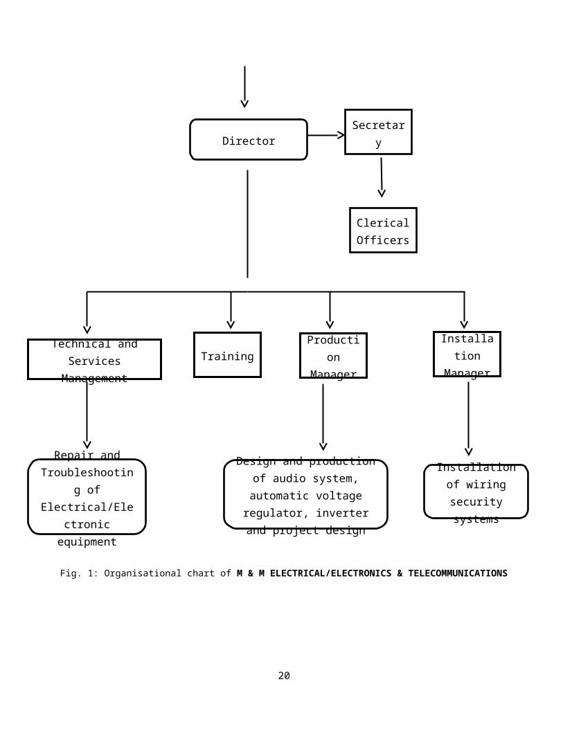
Figure 1 below shows the representation of the company.
2.4 Various Departments and their Functions
1. Technical Services and Management: This department has the
responsibility to make sure that the equipment in the workshop is
functional. They are also the department that repairs all the
faulty systems that a customer brings.
2. Training Department: One of the main visions of M&M
Electronics is to train young men and women who will gain skills
to work in companies of relative fields and also be able to have
their own companies and be self-employed and in turn create jobs
for other people. This department is responsible to make sure
that vision is fulfilled. They train students and they are also
18
responsible for the materials and tools that these students will
use. Courese like basic electronics, power inverter designs,
micro-controller basics and audio amplifiers are taken
3. Production Department: This department ensures that all the
jobs of production are being carried out, they also regulate
quality control. If a customer complains of a product they look
into it. They also make research so they can be able to provide
state of the art services to improve the company’s worth.
Products produces are solar inverters, power inverters, and audio
amplifiers.
4. Installation Department: After the production made by the
production department this department is to ensure proper
installation of equipment, it is possible that the equipment may
not have been produced by the company but they can be called upon
to perform installation services like solar power related
devices, satellite dishes, inverter systems and audio systems.
COMPANY ORGANISATIONAL CHART (Organogram)
19M & M ELECTRICAL/ELECTRONICS & TELECOMMUNICATIONS COMPANY
20
Director
Technical and Services
Management
Production
Manager
Installation
ManagerTraining
Design and production of audio system, automatic voltage regulator, inverter and project design
Repair and Troubleshootin
g of Electrical/Ele
ctronic equipment
Installation of wiring security systems
Clerical Officers
Secretary
Fig. 1: Organisational chart of M & M ELECTRICAL/ELECTRONICS & TELECOMMUNICATIONS
COMPANY
CHAPTER THREE
3.0 SKILLS AND KNOWLEDGE ACQUIRED
During the industrial attachment I was acquainted with a lot of
things which includes
a. Audio power amplifiers
b. The inverter system
c. Basic electronics
3.1 AUDIO POWER AMPLIFIERS
An audio amplifier is an electronic amplifier that amplifies low
power audio signal (signals composed primarily of frequencies
between 20 – 20,000 Hz, the human range of hearing to a level of
suitable for driving loudspeakers and is the final stage in a
typical audio playback chain. The preceding stage in such a chain
are low power audio amplifiers which perform tasks like pre-
amplification, equlisation, tone control, mixing/effects or audio
sources like record player, CD player and cassette players.
Most audio amplifiers require this low-level input to adhere to
line levels. While the input signal to an audio amplifier may
21
measure only a few hundred microwatts, its output may be tens,
hundreds or thousands of watts.
3.1.1 PRINCIPLES OF OPERATION
The audio amplifier works on the principle of magnetic
amplification. The magnetic amplifier is a static device with no
moving parts. It has no wear out mechanism and has a good
tolerance to mechanical shock and vibration. It requires no warm
up time. Multiple isolated signals may be summed by additional
control windings on the magnetic cores. The windings of a magnet
amplifier have a higher tolerance to momentary overloads then
comparable solid state devices. The magnetic amplifier is also
used as a transducer in applications such as current measurement.
22
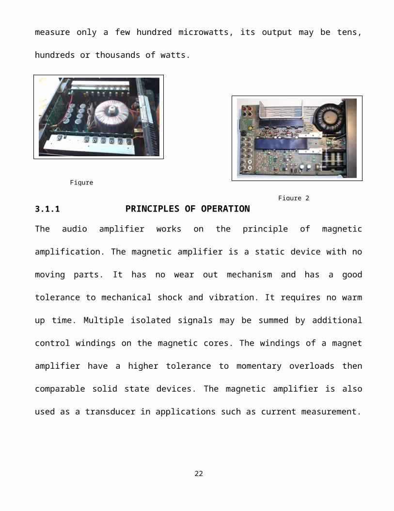
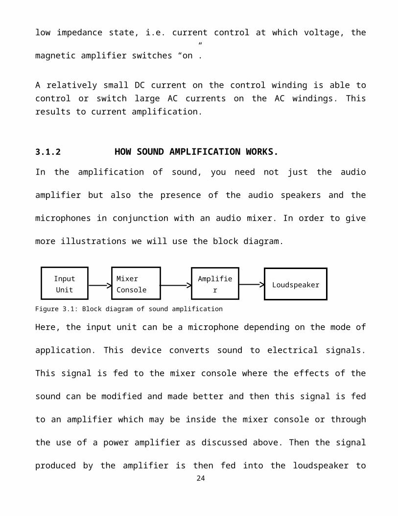
Figure
Figure 2

A magnet amplifier device may resemble a transformer but the
operating principle is quite different from a transformer
essentially the magnetic saturation of the core, a nonlinear
property of a certain class of transformer cores. For controlled
saturation characteristics, the magnetic amplifier employs core
materials that have been designed to have a specific B-H curve
shape that is highly rectangular in contrast to the slowly
tapering B-H curve of slowly saturating core materials that are
often used in normal transformers. The typical magnetic amplifier
consist of two physically separate but similar transformer
magnetic core, each of which has two windings – a control winding
and an AC winding. A small DC current from a low impedance source
is fed into the series – connected control windings. The AC
windings may be connected either in series or in parallel, the
configurations resulting in different types of magnetic
amplifiers. The amount of control current fed into the control
winding, sets the point in the AC winding wave form at which
either core will saturate. In saturation, the AC winding on the
saturated core will go from a high impedance state into a very
23
Mixer Console
Input Unit
Amplifier Loudspeaker
low impedance state, i.e. current control at which voltage, the
magnetic amplifier switches “on”.
A relatively small DC current on the control winding is able tocontrol or switch large AC currents on the AC windings. Thisresults to current amplification.
3.1.2 HOW SOUND AMPLIFICATION WORKS.
In the amplification of sound, you need not just the audio
amplifier but also the presence of the audio speakers and the
microphones in conjunction with an audio mixer. In order to give
more illustrations we will use the block diagram.
Figure 3.1: Block diagram of sound amplification
Here, the input unit can be a microphone depending on the mode of
application. This device converts sound to electrical signals.
This signal is fed to the mixer console where the effects of the
sound can be modified and made better and then this signal is fed
to an amplifier which may be inside the mixer console or through
the use of a power amplifier as discussed above. Then the signal
produced by the amplifier is then fed into the loudspeaker to24
drive it. When this is done this signal is then converted form
electrical signal to sound.
3.1.3 Maintenance and troubleshooting
In the maintenance of an audio speaker it normally requires that
you observe the sound waveform produced through the use of an
oscilloscope especially when it is running at a maximum output.
A good example of this type of maintenance is the adjustment of
the bias of the final amplifier tubes in an amplifier. Using a
sine wave test signal as input to the amplifier tubes in an
amplifier, the output tube bias may be adjusted is that the
output signal has no crossover distortion.
In any event where the audio power amplifier is not coming on, we
troubleshoot to ascertain the fault with a bit to fixing it.
These are the things we were told to check.
When we plug it and the amplifier does not come on at all,
we check for the fuse.
We check for the fuse in the external plug if it is bad, we
replace it.
25
If it is not that we check the fuse in the amplifier.
We also have signs to check if it actually a power problem.
For example if there is a power surge when it is being
plugged then we can infer that one of the components of the
power supply like the transformer or even the rectifier
diode is damaged.
If we check the above and they are still alright, then we
check the power transistors. This is most likely to be the
problem with almost all the panels we worked on. So when
this occurs we test for the damaged one and then replace it.
If the issues still persist we check for other components
like the capacitors to make sure they are connected to the
printed circuit board (PCB)
We also check the relay which is used for switching
There are even times when most or all the components in a
panel get burnt to much voltage being initially supplied to
it. In that case we have to design and construct a new
panel. This time around we can even produce a better one
26
that will suit the conditions of power supply in this
country.
By the time we are sure that the solution is perfect we then
test the equipment and make sure it is working properly.
Some other issues may also come up. The ones listed above
were amongst the common ones I encountered in the workshop.
3.2 The Inverter System
The inverter system is an electronics device that converts direct
current (DC) to alternating current (AC); the converted AC can be
at any required voltage and frequency with the use of appropriate
transformers, switching, and control circuits.
Solid-state inverters have no moving parts and are used in a wide
range of applications, from small switching power supplies in
computers, to large electric utility high-voltage direct current
applications that transport bulk power. Inverters are commonly
used to supply AC power from DC sources such as solar panels or
batteries. There are two main types of inverter. The output of a
modified sine wave inverter is similar to a square wave output
except that the output goes to zero volts for a time before27

switching positive or negative. It is simple and low cost and is
compatible with most electronic devices, except for sensitive or
specialized equipment, for example certain laser printers. A pure
sine wave inverter produces a nearly perfect sine wave output
(<3% total harmonic distortion) that is essentially the same as
utility-supplied grid power.
Thus it is compatible with all AC electronic devices. This is the
type used in grid-tie inverters. Its design is more complex, and
costs 5 or 10 times more per unit power. The electrical inverter
is a high-power electronic oscillator. It is so named inverter
because early mechanical AC to DC converters was made to work in
reverse, and thus was "inverted", to convert DC to AC. The
inverter performs the opposite function of a rectifier
We have three types of square wave inverter when we classify them
under the type of waveforms they produce
1. Square wave inverter: Square wave inverters were the first
invented inverter. Square wave inverter has odd number of
harmonics and can hardly be used on AC appliances except some
lights and fans. This kind of inverter eventually reduces the
28
life span of the appliances they power. This is also the cheapest
form of inverter.
2. Modified sine wave inverter: Modified sine wave is more like
the square wave which possesses less harmonic distortion compared
to square wave. The harsh corners from the square wave were
eliminated to transform it to a modified sine wave. This type of
inverter is the most seen in today’s market. Although it is less
harmful to devices compared to the square wave, it still heats up
the coil in filer due to large amount of harmonic distortion and
dissipates power.
3. Pure sine wave inverter: Unlike square wave and modified sine
wave, pure sine wave inverters maintain the best quality due to
the least number of harmonic distortions present in it. Usually
sine wave inverter is the more expensive of the two.
The advantage it has over the others is that it allows us to use
all AC appliances and reduces the humming noise of inductive
loads like fans. The figure below shows the output of a pure sine
wave form.
29

Before we go into the design of an inverter we must firstunderstand the basics.
So I will start with a block diagram
30
Oscillator
Circuit
Amplifier
Circuit
Switching
Circuit
Transformer
AC Output
AC MainsChange Over
Circuit
Output Socket
Battery Charger Battery
Sensing Unit
Figure 3.2: Waveforms of Square, modified and pure sine

3.2.1 Mode of operation
The power inverter I learnt during my IT operated in the
following way:
The DC voltage from a battery is fed to an oscillator which
produces signals that may be pure sine wave, modulated sine wave
or square sine wave. These signals can then be amplified by an
amplifier circuit which then increases the strength of the signal
in question. It should be noted that the amplifier section is not
compulsory. The switching circuit is made up of transistors
especially Metallic Oxide Semiconductor Transistors (MOSFETS) and
is connected in such a way that the output of the oscillator
switches them on and off at the frequency of the oscillator. The
transformer steps up the resultant AC from the switching circuit
to a value that can drive the required load.
The change over circuit enables the battery to connect to the
oscillator which in turn feeds the amplifier. The amplifier feeds
31
Fig. 3.3: Detailed block diagram of
the switching circuit while the switching circuit feeds this
signal produced to the transformer to get the required AC voltage
output for the inverter. The AC from the mains supply is also
connected to the changeover circuit so that it will feed the
output socket when there is power from the public AC mains. When
there is supply from the AC mains, the oscillator circuit will be
switched off to switch off the inverter. The AC main also feeds
the battery charger through the changeover circuit in order to
charge the battery. The sensing unit senses a number of
conditions like low battery, full battery and overload.
3.2.2 Design & Implementation of Inverter System
In the implementation of the above mentioned design, we are going
to be looking at the following components.
a. The required power transformer
b. The regulator circuit
c. The Oscillator circuit
d. The signal amplification circuit
e. The switching circuit
f. The battery charger32
g. The charge controller
3.2.2.1 THE POWER TRANSFORMER
In order to obtain the required specification needed to
construct we are going to perform some calculations.
Using the formula:
Where P = perimeter of bobbin
V = voltage
T = number of turns
Applying this formula we can therefore calculate the transformer
windings for both secondary and primary windings.
During my industrial training we were faced with the task of
producing a 5KVA inverter, with primary winding voltage of 48V,
secondary winding voltage of 220V and the inverting voltage to
be 290V.
33

The perimeter of the transformer bobbin was given as 27cm2
For the primary voltage we have that V = 48V, therefore the
number of turns needed is given as
For the secondary voltage winding at 220V
Therefore,
For the inverting voltage winding at 290V
It should also be noted that in getting the correct wire gauge
to be used for the inverter we must know the current that will
pass through the coil and use an approved chart to get the
appropriate wire gauge to use.
3.2.2.2 THE REGULATOR CIRCUIT
The regulator gives the oscillator its reference voltage and
determines the amount of power that drives the system. The
34

amplitude of the oscillator or timer is determined by the voltage
output of the oscillator and the current of the regulator
determines the stability of the oscillator. The zener diode D1
determines the regulating voltage ranging from zero to the
maximum applied voltage since to clips and clamps the base
voltage of the transistor Q1.
The transistor Q1 determines the regulator output current and the
maximum applicable voltage the regulator can regulate whiles the
resistor R1 gives a feedback between the input and regulating
reference voltage.
3.2.2.3 The Oscillator circuit
During my industrial training we used the SG3524 integrated
circuit (IC). This was used to generate a modified sine wave. The
figure below shows the IC pin-out
35
Fig 3.4: The regulator circuit
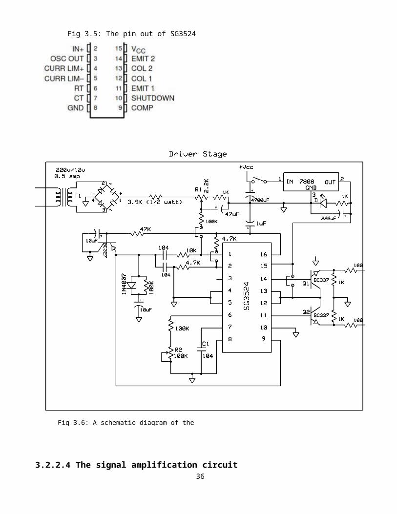
3.2.2.4 The signal amplification circuit36
Fig 3.5: The pin out of SG3524
Fig 3.6: A schematic diagram of the
The signal from the oscillator is fed to a dual input class AB
push pull amplifier to produce an alternating output with the
same waveform but with higher power, powerful enough to drive the
switching circuit.
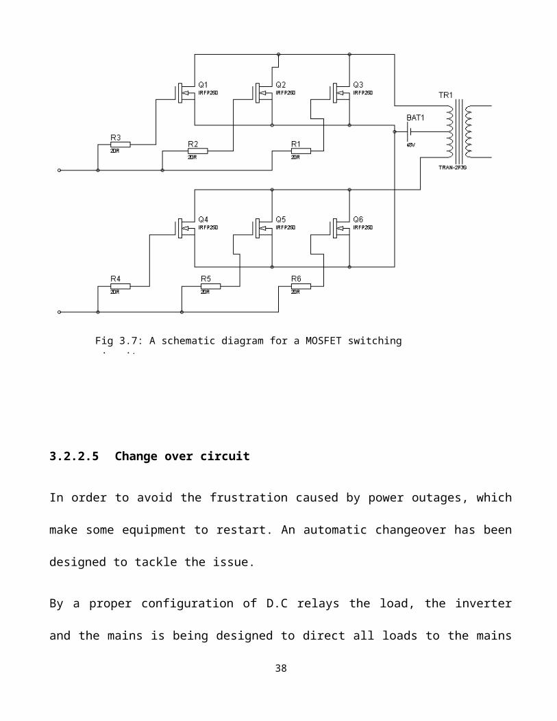
3.2.2.5 The switching circuit
After the amplification is done this signal is then fed into the
switching circuit. This circuit is made up of MOSFETs of which
the gates are all connected together and the signal from the
oscillator is fed in.
Also the drain of all the MOSFETs are all connected together and
then connected to the transformer, while the source are also
connected together and then connected to ground.
The frequency of the oscillation produced by the oscillator
switches, these transistors on and off at that same frequency
thereby generating the AC signal which then fed to the
transformer, the transformer steps up this AC signal to the
required voltage which can now be fed to the load.
37
3.2.2.5 Change over circuit
In order to avoid the frustration caused by power outages, which
make some equipment to restart. An automatic changeover has been
designed to tackle the issue.
By a proper configuration of D.C relays the load, the inverter
and the mains is being designed to direct all loads to the mains
38
Fig 3.7: A schematic diagram for a MOSFET switching circuit.
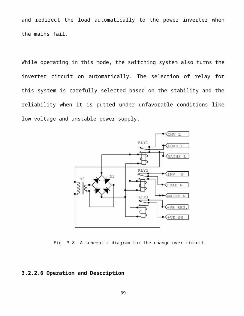
and redirect the load automatically to the power inverter when
the mains fail.
While operating in this mode, the switching system also turns the
inverter circuit on automatically. The selection of relay for
this system is carefully selected based on the stability and the
reliability when it is putted under unfavorable conditions like
low voltage and unstable power supply.
3.2.2.6 Operation and Description
39
Fig. 3.8: A schematic diagram for the change over circuit.
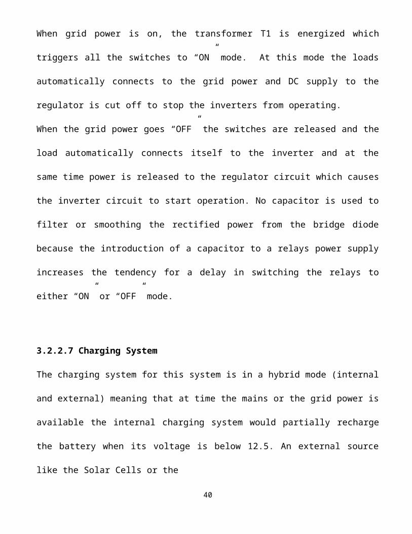
When grid power is on, the transformer T1 is energized which
triggers all the switches to “ON” mode. At this mode the loads
automatically connects to the grid power and DC supply to the
regulator is cut off to stop the inverters from operating.
When the grid power goes “OFF” the switches are released and the
load automatically connects itself to the inverter and at the
same time power is released to the regulator circuit which causes
the inverter circuit to start operation. No capacitor is used to
filter or smoothing the rectified power from the bridge diode
because the introduction of a capacitor to a relays power supply
increases the tendency for a delay in switching the relays to
either “ON” or “OFF” mode.
3.2.2.7 Charging System
The charging system for this system is in a hybrid mode (internal
and external) meaning that at time the mains or the grid power is
available the internal charging system would partially recharge
the battery when its voltage is below 12.5. An external source
like the Solar Cells or the
40

Wind turbine can also be connected to replace the internal
charger when the system is being used at a place where grid power
is not available. The internal charging circuit uses a
transformer less battery charging system instead of the normal
transformer type because the transformers produces great amount
of heat when the batteries are highly discharged which sometimes
eventually causes it to burn.
3.2.2.7 Battery Charger
When 220 volts AC is connected in series to a capacitor making
the AC tire which passes through the capacitor to make behave
like a pulse which created when the capacitor charges and
discharge. Since power cannot pass through the charger but only
store electrical power. The output from the capacitor is series
to the rectifier, changes the power to D.C ripples near zero
hertz making it conductive for battery charging. The diode only
used power stored in the capacitor. This procedure continues
until capacitor charges to full charge or the mains are
disconnected.
41
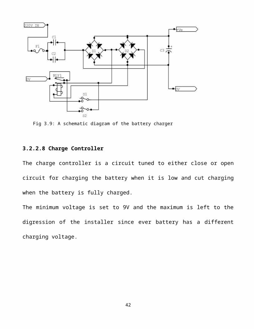
3.2.2.8 Charge Controller
The charge controller is a circuit tuned to either close or open
circuit for charging the battery when it is low and cut charging
when the battery is fully charged.
The minimum voltage is set to 9V and the maximum is left to the
digression of the installer since ever battery has a different
charging voltage.
42
Fig 3.9: A schematic diagram of the battery charger
3.2.3 Maintenance & Troubleshooting
During the course of my industrial training we did not only
produce the power inverters we also did some maintenance and some
trouble shooting. Also due to the fact that we are core
manufacturers, customers always come to us in order to repair the
faulty components.
One of the major problems we faced in the workshop was the
overheating of transformers. To tackle that issue we always had
to trace the fault by recoiling the power transformer, sometimes
the transformer had a bridge inside it or the transformer gets
burnt when any of these happened we recoiled the transformer.
43
Fig 3.10: A schematic diagram of a charge controller
Another problem we faced also was when the MOSFETs started to
overheat once the inverter was turned on so we just had to trace
the fault to the connection of these MOSFETs to their drain,
source and gates that were connected once the wrong connection
was rectified it would work perfectly.
Lastly, when the other circuits involved in the inverter circuit
seems to be faulty, problems may come from damaged transistors,
damaged relay, and any other damaged circuit. The needed action
to take was simply the replacement of such component and then
test for its functionality.
3.2.4 Precautionary measures
During my industrial training I was made to understand some
precautions that were needed to be taken. They are
1. Do not overload the inverter system so as to avoid blowing
up the inverter system.
2. Ensure that the polarity of the inverter system is not
reversed or bridged or else a hazard may occur.
44
3. Make sure that the battery being used is an original so that
it can serve you for longer hours.
CHAPTER FOUR
4.0 Basic Electronics
a. Delay Circuit using Operational Amplifiers
b. Power Supply Circuit.
c. Crossover circuit for Audio Speaker
45

4.1 Construction of a delay circuit using operationalamplifiers
The circuit uses RC circuit in combination with an Op-Amp
Comparator to accomplish the delay characteristic of a timer. In
the above diagram a voltage is applied across the R3-C1
combination. The input for the Op-Amp is tapped at the point
where R3 and C1 meet. This is the point where the positive
terminal of the capacitor gradually charges to the value of the
power supply. As the capacitor C1 reaches the Op-Amp's reference
voltage, the Op-Amp's output pin turns from High to Low, allowing
current to flow through the transistor, Q1, current enters the
base of the transistor and flows to the collector which acts as a
switch to turn the relay on. When the relay is on, current then46
Fig 4.1: A delay circuit with the

passes through the LED (causing the LED to glow). The time delay
can be controlled by changing the values or R3 or C1 or by
adjusting the value of the R1 and R2. For a new timer cycle to
occur, you must discharge capacitor, C1.
4.2 Regulated Power Supply Circuit
During my industrial training I also learnt how to build a power
supply circuit.
First I had to understand the basics using a block diagram
From the diagram we can infer that the AC voltage is fed into a
transformer which steps it down to a value defined by the voltage
specifications of the transformer. The output of the transformer
is then fed into a rectifier.
The rectifier converts the AC to DC. There are three kinds of
rectification which are the half wave reactivation, full wave47
AC Mains FilterRectifierTransformer
Regulated DC
output
Fig 4.2: A detailed block diagram of a power supply circuit
rectification (with the use of two diodes) and also the full wave
rectification with use of four diodes. The one that I constructed
was full rectification with four diodes. The output from the
rectifier is then being fed to the filter circuit in order to
reduce the ripple effect.
The filter circuit is of 3 types we can just connect the
capacitor in parallel to the rectifier or use the pi and T method
but this time we use an inductor.
Finally the output from the filter circuit is then fed into the
regulator which can be an IC or through the use of a zener diode.
It
should also be noted that we can also provide a variable
regulated power supply or a constant regulated power supply.
48
Fig 4.3: A schematic diagram of a dual rail regulated power supply circuit
Fig 4.4: A schematic diagram of a single rail regulated power supply circuit
Also the power supply can be a single rail power supply (can only
give an output of one polarity) or a dual rail power supply (can
give an output of both polarities).
It is important to note that in constructing a dual power rail we
must
use
a
center tapped transformer.
4.3 Crossover circuit
For certain loudspeakers that has both a woofer (bass) and a
tweeter a crossover circuit is being used because the balance
that the speaker gives depends on the amount of frequency the
sound produces.
49
The tweeter speaker is used for higher sound frequencies so it
will be connected to a high pass filter circuit, while the bass
50
Fig 4.5: Picture of a crossover circuit
Fig 4.6: Schematic diagram of a crossover circuit with a tweeter and to bass speakers
speaker is connected to the low pass filter in order for the
correct amount of frequency to pass through. Figure 3.16 shows a
picture of a crossover circuit, while figure 3.17 shows the
schematic diagram of a crossover circuit.
CHAPTER FIVE
5.0 SUMMARY, RECOMMENDATIONS AND CONCLUSIONS
5.1 PROBLEMS ENCOUNTERD DURING THE PROGRAM
I enjoyed my industrial training at M & M Electrical/Electronics
And Telecommunications Company but I was not left without
challenges.
1. No allowance
During my training I was not given any allowance to help
with the expenses that I had to take during the course of my
training like the transportation, feeding and then the
purchase of some needed equipment for work.
2. Distractions
51
During the course of training the colleague of my industrial
supervisor had many friends who came around. Sometimes they
would chat for a long time and this distracted us the
trainees. They would even ask us to go get something for
them in the midst of our learning. This did not help us to
learn very well.
3. Inefficient transfer of knowledge
I did learn a few things but I believe I would have learnt
more if we did not just only rely on “on the job training”
because we were not even given much jobs to do. Sometimes
the industrial based supervisor did not have enough time to
teach us some things. So there was transfer of knowledge but
it was not so satisfactory.
4. Lack of seriousness
Some of my colleagues were not even so serious. Some would
come in late and then some would not even come at all. So
whenever they were not around I was told to do things that
were not even related to my field of study.
5.2 Recommendations
52

SIWES is a very important programme in the life of any student
especially for those who would want to practice engineering.
SIWES has gone a long way to bridge the gap between what is done
in the university and what is done in the industry.
5.2.1 For the Industrial Task Fund and SIWES
I strongly recommend that ITF should keep visiting the students
on a regular basis i.e. at least 3 times in the space of the 6
months of the training so that these who are not serious will be
more dedicated to their place of work.
I also want to recommend that ITF should always liaise with many
companies to ensure that IT students do not have a hard time
finding a place of attachment.
I also want to recommend that in order for ITF to fulfill its
objectives in the career of students they should always ensure
that companies with the facilities to train engineering students
should be willing to accept a larger number of students than they
are doing now. This will go a long way to minimize the search
many students undergo before they find a place for attachment.
53
5.2.2 FOR THE COMPANY
I actually learned some useful things during my stay in M & M
Electronics. During my stay I observed a few things and I want to
recommend the following.
1. One of the things the company lack is a good marketer. There
are lot of persons in Anambra State and probably other
states who may need the services you provide but they need
someone to encourage or push them to buy it. A good marketer
with good skills can make you get more jobs and more money
so that you can even pay the trainees that come to the
company to work. One of the challenges I faced during my
training was lack of allowances during my stay there. So
doing this can be of good help in future.
2. The environment where the company is hidden. You provide
good services yet you are not well known in Awka. I will
54
advise that you either get another place or you make banners
or posters that will advertise your products and attract
much more customers. One of the challenges I also faced as
regards the venue was the fact that it was not conducive
enough for learning because of the level of noise and some
other distractions.
3. The customer relationship was not so wonderful, I am
actually trying to say that the way some customers get
disappointed because of a delayed job or a job not well done
that causes them to come back again over a short period of
time can continue to degenerate customer relationship. So I
recommend that they treat customers well so that in the long
run they would not lose many other customers.
4. In the world of business collecting loans to improve one’s
business is not that bad. I know you have a lot of things in
mind but then you need more packaging and packaging is going
to cost money. You have the capacity to become one of the
leading electronic schools in Awka but you have not provided
room for that. So I recommend that you get loans or apply
55

for programs that can fetch such loans in order to get more
money. One of the challenges I faced was that most of the
learning I did was always on the job training. It was only a
few times we sat down and learnt a few things. This did not
cause efficient transfer of knowledge. So I recommend that a
training school be set up so that the trainees can benefit
well and even be willing to pay.
5.3 Conclusion
In conclusion this industrial training has afforded me the basic
practical and theoretical knowledge that I may not have gotten
from the lecture room. It also gave me the opportunity to have a
feel of what it would be like after graduation when I start
working. It has also helped me to have knowledge of the
electronics industry.
5.3.1 Benefits I got after the SIWES program
More Confidence
56

During my training I developed confidence in constructing any
electronic circuit, because I was told to do that a lot. I can
even solder better than I used to.
With that to I can be able to analyse most electronic circuits.
Knowledge
During my SIWES program I was used to seeing many things on
electronics especially the components used in making a circuit. I
have an in depth knowledge of audio systems and how they operate
and also the inverter system.
Working Ethics
During this program I was learnt how to handle customers, and
also involved myself into many jobs that had to do with teamwork.
Exposure
57
I was exposed to many things like how to solder in a special
way, how to respond to faulty equipment and also how to respond
to customers anytime.
Networking
During my industrial attachment I made new friends in my field of
study, people I can be able to look up to and also seek their
help any time I have challenges whether it is during ny stay here
or beyond.
5.4 Suggestions to the improvement of Scheme
In order to make this scheme more interesting awareness needs to
be made corporate bodies on how industrial attachment students
should be treated. Any company that can train students that has
not yet started accepting students can collaborate with ITF and
see the best way they can start taking industrial attachment
students.
58

SIWES supervisors should be visiting us more often than they are
doing so that we can be encouraged to be very serious with this
programme.
SIWES should increase the pay and also pay the first half at the
beginning of the training and then pay the remaining at the end
of the training so that those who may encounter financial
problems can be able to cope.
59