MULTIPLE-STATION DIGITAL WIRELESS POWER ...
77
MULTIPLE-STATION DIGITAL WIRELESS POWER METERING SYSTEM by ADRL\N ARNOLDO PINEDA DAVILA, B.S.E.E., M.S.E.E. // A THESIS IN ELECTRICAL ENGINEERING Submitted to the Graduate Faculty of Texas Tech University in Partial Fulfillment of the Requirements for the Degree of MASTER OF SCIENCE IN ELECTRICAL ENGINEERING Approved August, 1999
-
Upload
khangminh22 -
Category
Documents
-
view
3 -
download
0
Transcript of MULTIPLE-STATION DIGITAL WIRELESS POWER ...

MULTIPLE-STATION DIGITAL WIRELESS
POWER METERING SYSTEM
by
ADRL\N ARNOLDO PINEDA DAVILA, B.S.E.E., M.S.E.E. //
A THESIS
IN
ELECTRICAL ENGINEERING
Submitted to the Graduate Faculty of Texas Tech University in
Partial Fulfillment of the Requirements for
the Degree of
MASTER OF SCIENCE
IN
ELECTRICAL ENGINEERING
Approved
August, 1999

\^\^w - > I V i * ' \
ACKNOWLEDGEMENTS
' ^ ' The author wishes to dedicate this thesis to his family. -"jGraciasportodo!"
/JO.iA^ The author wishes to thank Institute Tecnologico y de Estudios Superiores de
C^ 0 V Monterrey (I.T.E.S.M.) and Texas Tech University (T.T.U.) for the challenging
t opportunity of obtaining the Master of Science in Electrical Engineering degrees.
Special thanks to the Pineda and Davila families, in the USA and Mexico, for the
help and support throughout this unique opportunity.
To Dr. Armando Llamas Terres (I.T.E.S.M.) and Dr. Micheal E. Parten (T.T.U.),
thanks for serving as thesis advisors for this project. To Mr. Jesus Antonio Baez
(I.T.E.S.M.) and Dr. Michael Giesselmann (T.T.U.), thanks for serving as committee
members. To Dr. Federico Viramontes Brown (I.T.E.S.M.), thanks for the
professionalism and support. To the members of the Power Quality Laboratory at
I.T.E.S.M., thanks for the friendship and good luck with your endeavors. To the
undergraduate students of EE3332 and EE3333 (T.T.U.) who contributed to this project,
your work has been appreciated, thanks.
To the Hutton and Crawford families, thank you for your friendship.
To the many friends I have made while in graduate school in the USA and
Mexico, thanks for the memorable moments, support, and friendship.
'Say to yourself, 'My place is at the top.' Be king in your dreams."
- Andrew Carnegie 1889
u

TABLE OF CONTENTS
ACKNOWLEDGEMENTS ii
ABSTRACT v
LIST OF TABLES vi
LIST OF FIGURES vii
L INTRODUCTION 1
II. JUSTIFICATION OF WIRELESS POWER METERING SYSTEM 4
2.1 Introduction 4
2.2 Hard-Wired Demand Metering 4
2.2.1 Installation Considerations 6
2.2.2 Communication Standards Limits 6
2.3 Efficient Use of Electrical Energy 7
2.3.1 Power Factor Capacitor Location/Relocation 7
2.3.2 Redistribution of Loads and Abnormal Operation 8
2.3.3 Energy Savings 9
2.4 Other Benefits 9
m. SYSTEM DESIGN 10
3.1 Introduction 10
3.2 Base Computer Software 10
3.3 Communications Protocol 11
3.3.1 Network Control Access Scheme 11
3.3.2 Frame Structure 12
3.4 Base Station 15
3.4.1 Hardware 15
3.4.1.1 Microchip PIC 16C77/JW Controller 16
3.4.1.2 TIMAX232 16
3.4.1.3 Optrex LCD Module 17
3.4.1.4 Microchip EEPROMs 17
3.4.1.5 DS1306 Real-Time Clock 18
iii

3.4.1.6 Radiometrix Radio Packet Formatter IC 19
3.4.1.7 Radiometrix TX2-F-5 433.92 MHz UHF Transmitter 23
3.4.1.8 Radiometrix RX2-F-5 433.92 MHz UHF Receiver 24
3.4.2 Embedded Controller Software 24
3.5 Remote Station 27
3.5.1 Hardware 27
3.5.1.1 Method to Obtain Power Samples from Energy Metering IC 31
3.5.2 Embedded Controller Software 33
3.6 Designed PCBs 34
rV. TESTING 36
4.1 Introduction 36
4.2 Test of TIMAX232N RS232 Driver 36
4.3 Test of DS1306 Real-Time Clock 36
4.4 Test of SAMES 9604A Transducer 37
4.4.1 Test 1 Constant Resistive Load 37
4.4.2 Test 2 Stepped Resistive Load 41
4.4.3 Test 3 Voltage Swell/Sag 42
4.4.4 Test 4 Constant Lagging Load 42
4.4.5 Test 5 Constant Leading Load 44
4.4.6 Test 6 Constant Parallel Resistive and Lagging Load 45
V. CONCLUSION 47
5.1 Introduction 47
5.2 Project Cost Summary 47
5.2.1 Total Cost of Remote and Base Station 47
5.2.2 Cost Breakdown of Base Station 47
5.2.3 Cost Breakdovm of Remote Station 48
5.3 Flexibility of the Design 49
REFERENCES 51
APPENDIX 52
IV

ABSTRACT
This thesis describes the design of a multiple station digital wireless power
metering system for industrial plants. The objective of this thesis is the design of a
flexible multiple station digital v^eless power metering system.
Efficient use of electrical energy and reduction of energy costs can be achieved by
knoMdng the behavior of a plant's load. To run efficiently, industrial plant managers
must know load factor, power factor, the peak and average demand of the plant among
other variables. A monitoring system that provides the data necessary to calculate these
parameters is useful while one that is flexible and low cost is indispensable.
This project has been designed for and coordinated with the Department of
Electrical Engineering Division of the Efficient Use of Electrical Energy of the Institute
Tecnologico y de Estudios Superiores de Monterrey (I.T.E.S.M.) Campus Monterrey,
Nuevo Leon Mexico. This thesis manifests the continuation of a thesis at I.T.E.S.M.
entitled "Go-Back-N ARQ Multiple Station Digital Wireless Power Monitoring System
Design" by Adrian Amoldo Pineda Davila, M.S.E.E.

LIST OF TABLES
2.1 EL\/TL\-232-E and EIA/TIA-485 standards 7
3.1 Visual Basic interface screen command function descriptions 11
3.2PinfimctionsofRPC-000-DIL 21
3.3 SAMES 9604A register contents and addresses 29
3.4 Remote station command summary 33
4.1 Summary of test setups 37
4.2 Test 1 Partial listing of raw data 38
4.3 Test 1 fi^equency measurement results 38
4.4 Test 1 Calculated data, voltage and energies 39
4.5 Test 4 Calculated data, energies 43
4.6 Test 5 Calculated data, energies 44
4.7 Test 6 Calculated data, energies 45
5.1 Cost of one remote and base station 47
5.2 Base station cost summary 48
5.3 Remote station cost summary 49
VI

LIST OF FIGURES
1.1 Topology for power metering system 2
1.2 Wireless power metering system block diagram 3
2.1 LT.E.S.M. multiple-station hard-wired power monitoring system 5
2.2 Load profile of two transformers, I.T.E.S.M 8
3.1 Visual Basic interface screen 10
3.2 Frame structure 13
3.3 Data field structure, fi-ame type definitions 14
3.4 Expected communication on typical data transfer 15
3.5 Microchip EEPROM control byte format 18
3.6 DS 1306 oscillator circuit 19
3.7 Controller to RPC chip byte transfer timing diagram 22
3.8 RPC chip to Controller byte transfer timing diagram 23
3.9 TX2 transmitter block diagram 23
3.10 RX2 receiver block diagram 24
3.11 Contents of Base EEPROM and data.txt format 25
3.12 Communications timing diagrams 25
3.13 SAMES 9604A schematic 27
3.14 SAMES 9604A features 28
3.15 Bias circuit for rated values 30
3.16 Method to obtain power fi-om energy 32
4.1 Test 1 profile of active and reactive power 40
4.2 Test 2 stepped resistive load profile 41
4.3 Test 3 voltage swell/sag profile 42
4.4 Test 6 profile of active and reactive power 46
Ml

CHAPTER I
INTRODUCTION
Power metering m large industrial plants m the Monterrey, Nuevo Leon Mexico
area is a promising area of opportunity. By metering electrical power consumption
wdthin a complex, many of Monterrey's industrial sites can take measures to save money
by efficiently using electrical energy.
Remote stations are designed to acquire power measurements in intervals of 5
minutes 24 hours a day and record to local memory. A preprogrammed alarm in each
remote triggers them to transmit the previous day's measurements to a base station.
Since all stations are transmitting along a common bus they are programmed to transmit
at different times in order to time division multiplex the data at the base station. The base
station is designed to receive commands fi^om a PC running a Visual Basic control and
data acquisition program. The base station, when in monitor mode, wdll wait for
incoming data fi*om the remote stations and record any valid data (power measurement
data). Also, the base station is designed to store the incoming data to EEPROM and
upload to the PC when prompted by the user. Two hundred eighty-eight samples are
recorded for each remote station. This number of samples would represent one flill day
of power monitoring with samples taken every five minutes.
The power metering system designed here offers a flexible alternative to
hardwired systems. Although designed as unidirectional the system easily can
accommodate the changes required to make it bi-directional. Figure 1.1 illustrates the
topology of the power metering system. The bus is a wdreless 433.92 MHz channel. All
remote nodes are equipped vAth. transmitters while the base station is equipped with a
receiver. A deterministic bus access technique is programmed into the remote nodes'
controllers. Using a real-time clock, a preset internal alarm will trigger the remote nodes
to begin transmitting data on the bus once a day. Since the alarm for one node is set to go
off after giving the previous node sufficient time to complete its transmission the base
will receive all data in a time-division-multiplexed (TDM) manner.

Network Topology: Bus
,> -Station Bus Access Direction-
0 0 0 0
0
o o o
0 O O 6 0 -Station Bus Access Direction-
Figure 1.1 Topology for power metering system.
Figvu*e 1.2 illustrates the block diagram of the metering system. The base consists
of one IBM compatible PC, one Microchip PIC16C77/JW embedded controller, one
Radiometrix 433.92 MHz RX2 receiver, one Radiometrix RPC 000-DIL, one Optrex
DMC-16249B liquid crystal display (LCD), one Dallas Semiconductor DS1306 real-time
clock, one Texas Instruments MAX232N EIA/TIA-232-E transceiver, one NEC PS2501-
2 optical isolator, and eight Microchip 24LC256-I/P 32 Kbyte EEPROMs. Various
resistors, potentiometers, oscillators, capacitors, transistors, and LEDs complete the
design. A system control and data acquisition program developed in Visual Basic is
resident in the base computer.
The remote stations are designed exactly like the base station with two important
differences. First, a Radiometrix 433.92 MHz TX2 transmitter is used instead of a
receiver. Second, one SAMES SA9604A three phase energy metering IC is used as the
transducer. Various resistors, potentiometers, oscillators, capacitors, transistors, and
LEDs complete the design. The power monitoring is done on the secondary side of the
substation transformers. A substation is defined as a distribution point where a step-
down transformer sources a load.
Figure 1.2 depicts the block diagram of a 3-remote station system while Figure
1.1 shows that increasing the number of stations can easily be done with the same
arrangement. In this case, increasing EEPROM memory at the base would be required as
well as modifications to the base station controller firmware. For industrial plants, 16
stations is appropriate while a college campus, for example, may require many more.

1 1 : 1 —=^
1
IBM Compatible
Visual Basic DAQ Software
BASE STATION
Serial
upload
RTCDS1306
LCD
t
picie
EEPROM
T
OST
xjrtrolier
C77/JW -•03*-
• • : ; • • •
RPC-
000-
OIL
+ RXD — RECEIVER
V i 1
To Load i
1 V M . . ^ ^
I a D c
o p
u SAMES
SASeOSA
Enagy
-T^^MS)
RTCDS1306 .
LCD
» o S EEPROM ? 1 S .
_ I
REMOTE STATION 1
V
- RXA»-
COHTROLLER
PIC18C77/JW
RPC-
« • 000-
3*. OIL
^ TRANSUTTTER
n o To l-oad
2 Va D c
-m- \u. V2
oes
\ 1
Seri
al
4D
ow
nlo
ad
»
Up
load
• • X
EEPROM
T
REMOTE STATION 2
EnMw KeaehngIC • « —
RTC DS1306 .«>.
LCD - * —
•
-•RXA».
I 'RXR-CONTROLLER
Uicnx:t^> P1C16C77/JW
RPC- TXD-
000-
TX2-C3 92 MHZ TRANSUITTER
3 > OIL
V
To Load o Va.Bc X
T la.s z
o o
SAMES SA9605A
I En«tB»
-m-V3
Dee
,' •.
Seri
al
4D
ow
nlo
ad
»
Up
load
EEPROM
A
•
REMOTE STATION 3
RTCDS1306
- 'RST»j
,-:RXA»j
;-«.'RXRJ
LCD ; ( apc T~ - TX2-433 92 UH2 U _ | COMTROLiER j^^rXA-i ' ^ ^ T X D - » . ^ ^ ^ 5 ^ ^ ^ ^ —
n I itmOm : 000-PICieC77/JW -TXRH i<03>(
••D1>.
• • D O
000-
DIL
i
V
Figure 1.2 Wireless power metering system block diagram.
For this project importance was placed on the justification based on need and cost.
Chapter II spells out the project justification in detail. Specific design details are covered
in Chapter III while Chapter IV deals v^th the testing and implementation. Finally,
Chapter V concludes the text and includes any recommendations.

CHAPTER II
JUSTIFICATION OF WIRELESS POWER METERING SYSTEM
2.1 Introduction
The justification of a wireless power metering system must meet the dual
requirement of feasibility and practicality of application. To this end, it will be shovm
that a wireless system can be justified by considering the practical limits and costs of a
hard-v^dred demand metering system, the efficient use of electrical energy, and other
benefits.
2.2 Hard-Wired Demand Metering
Hard-wired communication systems are problematic in two key areas: installation
costs and transmission line losses. As the number of metering points and the distance
from the data logging computer increase these problems may circumvent the installation
of the system.
In 1994 a hard-wired monitoring system was developed and implemented on the
campus of I.T.E.S.M. located in Monterrey, Nuevo Leon, Mexico. The hard-wired
monitoring system (Figure 2.1) is comprised of many subsystems: current transformers,
instrumentation and power transformers, transducer/transmitter, wire pairs, receiver, data
acquisition card, presentation and results program.
The substation transformer of Figure 2.1 steps down 13.8 kV of line voltage to a
distribution level of 220 V. The transformer is A-Y connected. The secondary side line
currents vary fi*om 400 Amps for a 140 kVA substation and up to 2600 Amps for a 1000
kVA substation. Current transformers provide a proportional current signal no greater
than 5 Amps to instrumentation transformers. Instrumentation transformers are used to
lower the signal levels of the CTs and PTs to mA and mV levels for the electronics,
respectively. The transducer/transmitter calculates three phase real and reactive power
and provides a proportional firequency square wave output to the receiver.

13.8 («;V 220 V
'3E at CTs
\fJ UJ sjj
^^gpTs
.3E , 3
3 £
mtrumenlatior Transformers
Sup(p*v TraRsformer
Cif4
I '
Daia Ack|uis:iliGfi Card
n r r PO I I
Figure 2.1 I.T.E.S.M. multiple-station hard-wired power monitoring system.
Two two-wire pairs provide the physical link between the transducer/transmitter
and the receiver. The receiver contains 8 multiplexors to time-division multiplex the
square wave signals. Each multiplexor on the receiver can multiplex 8 signals. After
multiplexing, the proportional fi-equency signals are demodulated to DC voltages which
are fed to a DAS-1402 data acquisition card by Keithley MetraByte. A DAQ program
developed in Visual Basic controls the system.
Where possible, local vendors in Monterrey were used in the design allowing the
system to be attractive cost-wise. Although low-cost, this system is feature limited: it
only provides 3 phase real and reactive powers, and difficult point-to-point installation
and cable damage could occur [1].

2.2.1 Installation Considerations
In a given industrial plant a direct route ma not exist between metering points
and the data logging computer or system. The cost of making the physical circuit
connection may exceed the proposed benefit of installing a power transducer. An
alternative to costly installations exists m proposing a wireless power metering system
that will link two points without the need of a physical circuit connection.
As an example of such a problem, the department of Electrical Engineering at
I.T.E.S.M. Monterrey Campus experienced difficulties in connecting a hard-wired
demand transducer in a student residence building located off campus. "Estudiantes XV"
provides housmg for both graduate and undergraduate students of I.T.E.S.M. and is
considered an unportant load. Although a hard-wired demand metering system has been
in place throughout the majority of the campus since 1994, "Estudiantes XV" was only
metered until the summer of 1997. At that time, it was decided to bridge the distance and
make the physical circuit connection. An entire week elapsed, while workers attempted
to gain access to underground conduits under a major avenue, before the physical link
was made. Workers chiseled through concrete in an attempt to find any route to pass the
four wires required to connect the transducer.
2.2.2 Communication Standards Limits
There are two modes of operation for line drivers (generators) and receivers:
unbalanced (single-ended) and balanced (differential). The advantage of unbalanced data
transmission is when multiple chaimels are required; a common can be used. The
disadvantage of unbalanced data transmission is in its inability to realiably send data in
noisy environments. This is due to very limited noise margins. The sources of system
noise can include externally induced noise, cross talk, and ground potential differences.
Balanced data transmission requires two conductors per signal. In balanced data
transmission, the logical states are referenced by the difference of potential between the
lines, not with respect to ground. Differential data transmission nullifies the effects of
coupled noise and ground potential differences.
Data Terminal Equipment/Data Circuit terminating Equipment (DTE/DCE)
interface standards are set by two industry trade associations: Electronic Industry

Association (EIA) and the Telecommunications Industry Association (TIA). Although
the EIA and the TIA ha\e man communications standards two common standards
EIA/TL\-232-E (formerly, RS 232) and ELVTL\-485 are compared in Table 2.1 [2].
Table 2.1 EIA/TL\-232-E and ELVTL\-485 standards.
Parameter
Interface type
Driver loaded Output Voltage
Driver Open Circuit Voltage
Max Data Rate
Max no. transcei\ ers
20
EIA/TL\-232-E
Point to point
>|5.0V|
< 125 V 1
kbps (2500 pF load max)
—
EIA/TIA-485
Multiple, bi-directional
> | l .5V|
< 16.0V 1
10Mbpsg40ft .
100 kbps g 4000 ft.
32
EIAyTIA-232-E is a poor choice for high data rate requirements. EIA/TIA-485 is
a poor choice for applications where a high number of transceivers are required or
distances are large. Both are poor choices in installations where a point to point physical
link is not possible.
2.3 Efficient Use of Electrical Energy
Efficient use of electrical energy is possible fi-om a monitoring system whether
wireless or hard-wired. The efficient use of electrical energy is the act of using the
metering data fi-om the monitoring system and based on the demand profiles make
informed decisions about control or better use of the supplied power.
2.3.1 Power Factor Capacitor L ocation/Relocation
Power profiles of all substations throughout an industrial plant permit the
correction of the power factor (PF) of the utility supply by clear knowledge of the exact
amount of VARs needed. Power metering also allows the connecting of power factor
correcting capacitors in a distributed manner making the entire system less susceptible to
harmonic resonance in the presence of harmonics, reduces the effects of high transient
7

turn on currents, and allows for the detection of unbalanced voltages. Power factor
correction is advantageous for plants in the Monterrey area as this avoids costly power
factor penalties fi-om tiie Mexican Federal Electricity Commission. Improved power
factor also reduces I R losses in the distribution system.
2.3.2 Redistribution of Loads and Abnormal Operation
0:00 6:00 12:00 hours
18:00
A. "Estudiantes IT, 150 kVA
i
180
150
120
90
60
r^>H^^''''MA'''V.
w
.^^-J-^"»>^,.u.*~J ;
- I -
0:00 0:00 6:00 12:00 hours
18:00 0:00
B. "Estudiantes" Cafetena, 225 kVA
Figure 2.2 Load profile of two transformers, I.T.E.S.M.
A power monitoring system also allows for the detection of abnormal or
unexpected operation in the distribution transformers. As an example, the hard-wired
monitoring system developed and implemented at I.T.E.S.M. Monterrey Campus
detected transformers that were operating above their nominal ratings and transformers
that operated much below rated value, see Figure 2.2. The 150-kVA transformer of a
student residence building, known as "Estudiantes II," operated above its rated value
while the 225-kVA transformer of cafeteria "Estudiantes" operated well below its rated
value. Swapping these transformers stopped overheating in the 150-kVA transformer,
heating which deteriorates winding insulation and reduces transformer life.
The monitoring system at I.T.E.S.M. detected another abnormal condition. Two
750 kVA, 13.8 kV/220 V A-Y transformers connected in parallel, on both primary and
secondary, source a two-tower (North and South) building known as "CETEC." Tap
changes were needed on the transformers and hence were disconnected from the main
supply. Upon re-energizing the transformers, workers unwittingly only connected one. 8

the south tower transformer. The north tower transformer, energized through its
secondary, appeared as a reactive load requiring only magnetization current. The load
profile for that day indicated the problem.
2.3.3 Energy Savings
Through a demand profile analysis, load factor can be easily determined during
any period of time. Improvement in load factor can also be achieved by redistributing
loads where possible and changing the time of day some loads operate. Reducing the
load factor implies a decrease m the average demand billed thereby lowering energy
consumption. Off-peak power is cheaper than during peak hours. Redistributing the
operation of loads not needed during peak hours also reduces energy bills. With the
objective of the efficient use of electrical energy, other uses of a monitoring system
include consideration of the installation of high efficiency motors, installing variable
frequency drives, and detection of motors that operate with little load. In general a
monitoring system is practical as it provides a means for the better use of electrical
energy [3].
2.4 Other Benefits
Once fixed power factor correcting capacitors are in place the next step is the
automatic connection of power factor correcting capacitors based on feedback
information from the monitoring system. At the present time, I.T.E.S.M. has developed a
single substation prototype automatically switched capacitor bank integrated with the
current hard-wired transducer. A more attractive approach would be the switching of
capacitors from the central logging station. This control could easily be programmed into
a wireless monitoring system.
The justification of a wireless power monitoring system is complete. The
advantages in terms of the efficient use of electrical energy and practicality have be
spelled out. Next, a detailed description of the design of a multiple station power
monitoring system is offered.

CHAPTER III
SYSTEM DESIGN
3.1 Introduction
The design of this digital wireless power metering system can be separated into
five separate modules: base computer software, communications protocol, base station
hardware and embedded controller firmware, and remote station hardware and embedded
controller firmware.
3.2 Base Computer Software
A Visual Basic program was written to provide the basic command and control
functions of the metering system. Commands are sent via the Visual Basic user interface
software to the station, base or remote, embedded controller's hardware universal
asynchronous receiver transmitter (USART). A Texas Instruments MAX232N is used to
interface between the chip US ART and the computer's serial port.
Figure 3.1 Visual Basic interface screen.
Figure 3.1 depicts the program that may be used on the base station and remotes.
Seven large buttons indicate valid commands to be sent to the given controller. On
10

power up or a power reset the embedded controller's program waits for a command from
the user.
Table 3.1 describes the fimctions of all buttons on the interface screen.
Table 3.1 Visual Basic interface screen command fimction descriptions.
TTON
POWER
MONITOR
UPLOAD DATA
PROGRAM REAL
TIME CLOCK
PROGRAM RTC
ALARM
SEND
YES
NO
DESCRIPTION
Sends ASCII "A" to base controller USART via serial port. Will place the given station in monitor mode. The base station will await data from the remote. The remote stations will record power measurements every five minutes and transmit data towards the base once a day.
Sends ASCII "B" to the given controller. The controller will upload 288 samples of data in rows of 43 bytes. Data is uploaded in packets due to VB buffer size limits.
Sends ASCII "C" to the given controller. Once "C" has been sent the VB program acquires date and time from the host computer's internal clock and sends, in 8 bit decimal format to the controller's USART, the date/time stamp in the following order: year, month, date, day of the week, hour, minutes, seconds.
Sends ASCII "D" to the given controller. Once "D" has been sent the VB program user selected hour and minute along with the seconds (default value of 0). This corresponds to the contents of ALARM 0, which when set signals to the remote station to transmit data towards the base.
Will send contents of TEXT 1 window to the base controller. This feature is used for testing and debugging.
Sends ASCII "y" to base controller USART.
Sends ASCII "n" to base controller USART.
3.3 Communications Protocol
3.3.1 Network Control Access Scheme
A deterministic or non-contention access scheme is implemented in this design.
Deterministic implies controlled access to the network. One station at a time can access
the channel provided that an alarm set by the real-time clock for that station has been set.
Synchronization of the real-time clocks is necessary for this to succeed, as such battery
backup is required by the DS1306 to prevent loss of tune due to power supply failure. By
programming the alarms to set at least 3 minutes after the previous station's alarm has
been set, each station accesses the bus not only during a unique time period but allows
sufficient time for the previous station to transmit its data.
11

3.3.2 Frame Structure
With the nen\ork access control scheme defined, the next step is to define the
structure of the fi-ames being transmitted through the bus.
Figure 3.2 depicts the frame structure used in this design. A data fi-ame in general
is made up of four parts: preamble, fi-ame synch, data, and error checking. The preamble
is a 3.2 ms 20 kHz pulse train that allows other units to identifS- the incoming data fi-ame.
The fr-ame synch is a special 7-bit Barker sequence used to sTichronize the data sheer of
the recei\er to incoming data. The data portion of the frame is the packet we wish to
transmit. Finally, the last part of the data frame is a checksum bte that checks for
o\ erall packet integrit.
Four fields define the data portion of the fi^me structure as follows. First is the
RPC Control field (RPCC). This is a one-byte control field whose purpose is to tell the
RPC chip how many total btes are in the data packet. More specifically, the lower 5 bits
of the byte provide a 5-bit ble count. The upper three bits are used for preamble control
and to designate the bie as a data b>te or a memory bte. A memory tpe bie is used to
change the configuration of the RPC chip. Second, is the Control Field (C). This is a
three-ble control field whose purpose is to identify the purpose of the firame
(Frame_T>-pe, 1 bie) and the number of the fi-ame (Frame_Number, two bies). Third,
is the Address Field (A). This is a two byte wide field with the MSB indicating the
source station address and the LSB indicating the destination station address. Lastly, is
the 22 ble wide Data Field (D). For this power monitoring system there are 5 different
fi-ame types that may be placed on the bus. Figure 3.3 illustrates the different tpes of
fi-ames as defined b the different types of contents in the Data Field.
12

FRAME STRUCTURE
Preamble Frame Date Error Check Synch Symbol Coding
-Variable-*-* 7 Bit *-<—1 Byte—•<—3 Bytes » * 2 Bytes—^4-22 Bytes-^^—1 Byte—•
RPCC C A D Error Check
T3
Fie
o -Q N E x S ^ n^° Q- CM
T3
Iel
ce
U. c
o 3->. o CO CO
$ e 1 E .S 1 S o
U. CD
p
Ii .
o ^-. c O
o o a. a:
TJ
c i L
rol
c o O
T3 C Ii.
ess
• o •o <
T3
0) ii.
a CB O
T3
ii.
u o O O Q. (T
FIELD STRUCTURES
RPCC
^^-^ Bit-*^ 2 Bit P-^ 5 Bit-
PT WU1 WUO BC4 BC3 ' BC2 BC1 BC1
S . ; > . | O _ C 0 Q _ S O X H o ; - i ? fe S 3 5 o I I i I E o g w u - m g o - ^ (S
tB II II ' S o •<- O •<-Q . O T - 1 Q - O O T - T - ] lO
-8 Bit X 16 Bit-
Frame Type Frame Count
1? S X
I - .« ^ 2 « U.
g CM 2 E ® S 9 3 o a 3 o
-8 Bit •-• 8 Bit-
87 S6 S5 S4 S3 S2 S1 SO D7 D6 D5 D4 D3 D2 j 01 DO
c O
? ^ I ^ o • • •
S c 2 £ t 5 < o 2. < o 2-
Figure 3.2 Frame structure.
13

DATA FIELD (22 bytes)
(type 0) Command Frame
1 Byte »-4 -16Bit- - • < -
Command Type
-19 Bytes-
Frame Number Max not used
(type 1)ACK Frame
< 8 Bit »-4— -16Bi t - -»-*- -19 Bytes-
Frame Type Frame Number notussd
(type 2) NACK Frame
•< 8 Bit • < -16 Bit- - • • - -19 Bytes-
Frame Type Frame Number ^fK^used
(type 3) Time Stamp / Per Phase Energy Frame
< 3 Bytes ^ ^ -18 Bytes- - • ^ 1 -
hour min sec EA Active EA Reactive EB Active EB Reactive EC Active EC Reactive not
i«ed
Bit
Bit
Bit OQ
CM
4B
CM 4
B
eg
4B
(N
4B
l
r>j
4B
l
CNJ
Byt
(type 4) Date Stamp / Per Phase Voltage and Frequency Frame
< 4 Bytes >^ -18 Bytes-
day date mo yr VA fA VB fB VC fC
. t i
m 00
.-ti m oo
. t i OQ
oo
* i CQ CO
OQ
•<>• Ol
m • *
CM
OQ 1 -CM
OQ • *
CM
00 • *
CM
OQ • »
CM
(Type 0) Command Frame. A command packet is transmitted with a one-byte wide command plus a 16 bit number (Frame Number Max) to indicate the number of the last frame to be expected in the fransmittal.
(Type 1) ACK Frame. *Reserved for future use* An ACK packet is transmitted with a one-byte wide frame type and the number of the frame that was acknowledged in the data field.
(Type 2) NACK Frame. *Reserved for future use* A NACK packet is transmitted with a one-byte wide frame type and the number of the frame that was not acknowledged in the data field.
(Type 3) Time Stamp/Per-Phase Energy Frame. A time stamp/per-phase energy frame consists of a 3 byte time stamp followed by 18 bytes of energy data per phase.
(Type 4) Date Stamp/Per-Phase Voltage and Frequency Frame. A date stamp/per-phase voltage and frequency frame consists of a 4 byte date stamp followed by 18 bytes of voltage/frequency data per phase. A type-3 frame followed by a type-4 frame contaias the contents of 1 measurement sample.
Figure 3.3 Data field structure, fi-ame type definitions.
Figure 3.4 illustrates the packets transmitted on the bus and by which station for
typical data transfer. All data bytes within the packets are given in decimal unless
otherwise noted.
14

Expected Communication
(byt*) 0 9 10 II 12 13 14 15 Ii 17 18 19 2D 21 22 23 24 2 M 77
g«U RPCC 9 I 10 I 11 1 12 I 13 I 14 I i ; I 1« I 17 i 18 i l i l I a I i ' puniQi Sb'ftes J Z Q l ftamacUBtbM ftott to • I 2 I 3 I
bout mtn sec EA Active <l«y I date | moii [ jtia VB
how mm JBC EA Actavo
day 1 (fate [ mon | y a n I I V B
0 hour flan 8ec EA Re»cliTt I EB Active flay A ^ mon yew ] VB VC
aun sec day date mon year j I
Station X DATA 3 27 EARe&cUve | EBActrra" stafaonX DATA 4 diy
"Inot used
Figure 3.4 Expected communication on typical data transfer.
This transmission assumes that the base station was placed in "Monitor" mode
prior to the time the TRANSMIT ALARM for station 1 was set. First station one's
TRANSMIT ALARM is set and station one begins it's transmission with a command
packet. The command frame's Data Field indicates the maximum number of frames (n)
in the message. Since it takes two frames to transmit all of the data for one measurement
(i.e. one sample) for 288 samples, one day of monitoring at 5 minute intervals, 576
frames would be required to transmit all of the data for station 1. After station 1 has been
given sufficient time to transmit its data, station 2's TRANSMIT ALARM will be set and
station 2 will begin its transmission in the exact same way as station 1. The base station
will test each incoming frame to see if the last frame has been received based on the
frame number maximum it received at the beginning of the transmission.
3.4 Base Station
As mentioned earlier, the base station controller receives commands from the PC
through a serial interface. Once a command is received the base controller may only be
interrupted, prior to completing with its task, via a manual reset. In order to describe the
base station in more detail a closer look is needed at the hardware and software of the
controller.
3.4.1 Hardware
The hardware of the base station consists of one IBM compatible PC, one
Microchip PIC16C77/JW embedded controller, one Radiometrix 433.92 MHz RX2
receiver, one Radiometrix RPC 000-DIL, one Optrex DMC-16249B liquid crystal display
15

(LCD), one Dallas Semiconductor DS3106 real-time clock, one Texas Instruments
MAX232N ELVTIA-232-E transceiver, one NEC PS2501-2 optical isolator, and eight
Microchip 24LC256-I/P 32 Kbyte EEPROMs. Various resistors, potentiometers,
oscillators, capacitors, transistors, and LEDs complete the design.
3.4.1.1 Microchip PIC 16C77/JW Controller
The Microchip PIC16C77/JW was chosen due to its compatibility with Micro
Engineering Labs, Inc. PicBasic Pro Compiler. The programs are written in a derivati\ e
basic code making prototyping very rapid. Assembly language code can be intermixed
v^th the basic program, using "@'* for single line insertion or "ASM" followed by an
assembly code block then "ENDASM", for a very powerful means of executing detailed
tasks. Microchip's MPLAB development and simulation software, available online, was
configured with PicBasic Pro to compile programs wdthin its environment. MPLAB
provided a complete editor, compiler, and programmer package. Microchip's Pic Start
Plus programmer was used to program the micro-controller EPROM.
The crystal chosen for the PIC16C77 is a FOX200 20 MHz series crystal. A
series crystal is designed to operate at the desired frequency without the need of external
capacitors, as such low component count is achieved [5]. A 10-Q series resistor is
included to limit the feedback current.
3.4.1.2 TIMAX232
The laptop communicates serially to the USART of the controller. A Texas
Instruments MAX232N EIA/TIA-232-E transceiver is required to convert TTL level
signals to EIA/TIA-232-E and vice versa. Three connections are required to the serial
port: TX, RX, and Vss. These are connected to pins 2, 3, and 5. respectively, of a DB-9
connector. The laptop serial port is then connected to the DB-9 connector. The base
controller's hardware USART is located on P0RTC.6 (TX) and P0RTC.7 (RX). These
pins are connected to tiie TI MAX232N pin 10 (T2IN) and pin 9 (R20UT) via a 2
channel NEC PS2501-2 optical isolator. To isolate tiie signals the RTS signal from the
serial port, pin 7 on the DB-9 connector, is used to power the MAX232N and the PC side
of the optical isolators. A 5-volt zener diode, 100 current limiting resistor, and 220 nF
16

capacitor are used to form the 5 volt supply. For this to work, RTS must be enabled in
the Visual Basic control program's Microsoft Comm Control module. External bias
electrolytic capacitors are used to store charge to provide RS232 levels of ± 10 V to the
serial port. The baud rate is set within the base station controller's software
(HSERBAUD) and witiiin the Visual Basic interface program's Microsoft Comm
Control module. Both baud rates are set to 9600. This provides relatively fast uploads
while reducing errors.
3.4.1.3 Optrex LCD Module
An Optrex DMC 16249B LCD module, in 4-bit mode, is used to show the current
status of the base station as well as to notify the user of needed input. PORTA.O to
P0RTA.4 and PORTE.O are used to interface with tiie LCD module. The Optrex LCD
module was chosen as it uses a Hitachi HD44780 driver which is compatible with the
PBASIC compiler used to program the Microchip PIC16C77/JW controller. For example,
in order to display "hello" using a PBASIC program and a compatible LCD display the
instruction LCDOUT "hello" is all that is required.
3.4.1.4 Microchip EEPROMs
Eight I2C compatible Microchip 24LC256-I/P serial EEPROMs are connected on
a common bus to the controller and provide up to 8x32 Kbytes of data storage. PORTD.O
(DPIN) and PORTD.l (CPIN) are connected to the SDA and SCL lines of the EEPROM
common bus. SDA (DPIN) is a bi-directional pin used to transfer addresses and data into
and out of the EEPROM. It is an open drain terminal therefore the SDA bus requires a
IkQ. puU-up resistor.
A control byte (cont) in the PBASIC instruction to read and write. I2CREAD and
I2C WRITE, determines which EEPROM is accessed. The address of tiie first EEPROM
is set to 0:0:0 (A2:A1:A0), the second to 0:0:1 (A2:A1:A0) and so on while the last is set
to 1:1:1 (A2:A1:A0). Figure 3.5 shows that the control byte of the EEPROM consists of
a 4-bit control code of b'1010 binary for the 24LC256. The next three bits are the chip
select bits (A2:A1:A0) that allow the use of up to eight 24LC256 devices on the same
bus and are used to select which device is accessed [6].
17

ReadA/Vrite Bit —
C<witrolCode CNp Select
Bits T
A2 Al AO FVW
Figure 3.5 Microchip EEPROM control b>le format.
The last bit of the control byte defines the operation to be performed. When set to
a one a read operation is selected, and when set to a zero a write operation is selected.
I2CREAD and I2CWRITE will automatically set or clear this bit respecti\ ely. As such
tiie control byte that must be specified when using I2CREAD and I2CWTIITE is simply
b'lOlOdddO where ddd correspond to A2:A1:A0. ft's important to note that in order to
increment tiie control byte address to select tiie next device it is tiie DEVICE ADDRESS
portion of the control byte that must be incremented and not simply the control byte.
3.4.1.5 DS1306 Real-Time Clock
A Dallas Semiconductor DS1306 is used to keep the real time of the system. This
device counts seconds, minutes, hours, date of the month, month, da\' of the week, and
year. It can provide leap year compensation until the year 2100. This real-time clock
was chosen because it provides for two programmable alarms, battery backup supply pin,
plus most importantly a Serial Peripheral Interface (SPI) compatible with the Microchip
PIC16C77.
A three-volt lithium battery is connected to pin 2 of the DS1306 to prevent time
loss in the event of power failure. SERMOD (pin 9) is connected to ground, this places
the device in serial three-wire communication mode. As such, SDO (pin 13) and SDI
(pin 12) must be connected together and tied to SDA (P0RTD.4) of the PIC controller.
In summary, the three-wire communication consists of lines CE (P0RTD.6), SCLK
(PORTD.5), and SDA (P0RTD.4) connected from tiie PIC controller to tiie DS1306.
18
01
Figure 3.6 DS1306 oscillator circuit.
The crystal chosen for the device is a FOXNC38 tuning fork watch crystal with a
specified load capacitance of 12.5 pF, CL. Figure 3.6 illustrates the oscillator ckcuit for
tiie DS1306. If C1=C2=5.6 pF, CDS1306=6 pF (from datasheets), and a stray capacitance
of CS=4 pF assumed (3-5 pF typical) then:
^5.6-5.6 C C eq C i + Q 5.6-H5.6
-h 4.0+ 6.0 pf = \l.%pf
'• ^eq ~ Q •
With the correct load capacitance connected to the DS1306 crystal the crystal will
operate at the designed frequency hence the real-time clock wdll keep accurate time. An
18 kQ resistor is added in series with the oscillator to prevent oscillator overdrive.
3.4.1.6 Radiometrix Radio Packet Formatter IC
A Radiometrix RPC-OOO-DIL packet formatter IC (RPC chip) is used to receive
and transmit data frames. "A data packet of 1 to 27 bytes downloaded by the Host micro
controller into the RPC's packet buffer is transmitted by the RPC's transceiver and will
"appear' in the receive buffer of all the RPC's within radio range. A data packet received
by the RPC's transceiver is decoded, stored in a packet buffer and the Host micro
controller signaled that a valid packet is waiting to be uploaded."[7] The host controller
may transfer up to 28 bytes to the RPC chip for transmission. The first byte of the 28
byte packet maximum is a control byte. The control byte provides control information in
the form of 3 flag bits and a 5 bit byte count which indicates the number of bytes, itself
included, that are to be transferred to the RPC chip by the controller for transmission via
the transmitter. Thus the data portion of the packet contains 1 control byte and a
19

maximum of 27 user data bytes. The data rate is given by the following formula for a 10
MHz oscillator:
DR = l^^siis!£L. bit I sec = 39.0625 kbit I sec 256
Once the data portion of the packet is transferred to the RPC chip the actual packet that is
sent to the transmitter is made up of four parts.
Preamble. A 20 kHz square wave has the function of allowing the data slicer in a
remote receiver to establish the correct slicing point, then once the receiver settles, the
remaining portion is used to positively identify and phase lock on to the incoming signal.
The preamble time is set at the default 3.2 ms.
Frame sync. Synchronization of the data is achieved with a Barker sequence of 7
bits. This synch sequence allows the receiving RPC chips to positively identify incoming
data.
Data. Upon receipt of a data packet to transmit the RPC chip codes each byte into
a 12 bit symbol. Provides 50:50 bit balance, i.e., 6 ones and 6 zeros. The RPC chip
allows no more than 4 consecutive ones or zeros minimizing the low frequenc\
components in the code. Provides a minimum Hamming distance of 2 meaning each
code generated is different from any other code by a minimum of 2 bits. Onl 256 of
4096 possible codes are valid. This is 6.25%, which implies a 93.75% probability of
trapping a byte error.
Check Sum. The receiver checks each symbol for mtegrity as such an 8-bit
checksum is used to test for overall packet mtegrit\\ The check sum is also coded into a
12-bit symbol.
While receiving, decoding of a transmitted packet is also done in 4 stages.
Search. The RPC chip decoder searches tiie radio noise on the RXD line of tiie
recei\'er for tiie preamble of 20 kHz. A 16 times over-sampling detector computes tiie
spectral level of 20 kHz in 240 samples of the RXD signal. If the level exceeds a pre-set
threshold, the RPC chip will attempt to decode a packet.
Lock-m. The 240 samples from the over-sampling detector are used to compute
the phase of the incoming preamble and s\Tichronize the RPC chip's internal recover
20

clock to an accuracy of ±2 |j,s. The incoming data is sampled at the bit midpoint by the
recovery clock and serially shifts the data through an 8 bit comparator. The comparator
searches the sampled data for a frame synch byte and will abort this process if the packet
fails to maintain a certain level of integrity. When the frame synch byte is detected, the
RPC chip will attempt to decode the data packet.
Decode. Twelve bit symbols are now read, decoded, and placed in the receive
buffer. If an mvalid symbol is received the RPC chip will abort the current process.
Check Sum. This last byte is decoded and verified against a sum of all received
bytes by the receiving RPC chip. If this matches, then the data packet is valid and !RXR
is pulled low to inform the host controller that a valid packet has been received and
awaits in the receive buffer. !RXR in tiiis case is connected to PORTB.O of the
PIC16C77/JW controller and configured as an external interrupt.
The RPC chip is connected in parallel with the PIC16C77 as depicted in the
appendix base station and remote station schematics. P0RTD.7 (!RST) is used as the
reset line, active low, from the PIC controller to the RPC chip. PORTB is used to pass
and receive data to and from the RPC chip. Table 3.2 details the pin functions of the
RPC chip.
Table 3.2 Pin ftmctions of RPC-OOO-DIL
Name
TXR
TXA
RXR
RXA
DO
Dl
D2
D3
Pin
6
7
8
9
2
3
4
5
Pin Function
TX Request
TX Accept
RX Request
RX Accept
DataO
Datal
Data 2
Data 3
I/O
I/p
0/P
0/P
I/p
Bi-dir
Bi-dir
Bi-dir
Bi-dir
Description
Data transfer request from HOST to RPC
Data accept handshake back to host
Data transfer request from RPC to HOST
Data accept handshake back to RPC
4 bit bi-directional data bus. Tri-state between packet transfers. Driven on receipt for Accept signal until packet transfer is complete.
Figures 3.7 and 3.8 illustrate the handshaking signals and timing involved in byte
transfers to and from the RPC chip, respectively. To transfer a byte to the RPC chip from
21

the controller P0RTB.2 (!TXR) is brought low by the PIC16C77/JW controller. The
RPC chip will accept this request by setting !TXA (P0RTB.3) low. Now the controller
proceeds to place the least significant nibble of the data byte on the bi-directional bus (DO
-D3) and signals the readiness of this data to the RPC chip by asserting P0RTB.2
(!TXR) high. Once the four bits have been accepted the RPC chip will assert !TXA
(P0RTB.3) high. The cycle is repeated for the most significant nibble as well as any
subsequent data bytes.
TX-Request (TXR)
transfer request data present
1 /
TK-Accept (TXA.)
request accept
\
DATA (4 lines D0-D3)
data has been read
1 /
• data ma; change •
LS nibble I
MS nibble
<-least significant nibble •> •< most significant nibble
•< Ibyte
I
Figure 3.7 Controller to RPC chip byte transfer timing diagram.
Figure 3.8 shows that receiving a data byte from the RPC chip is similar. Two
main differences are that the RPC chip is now driving the data bus and the hand shaking
lines are PORTB.O (!RXR) and PORTB. 1 (!RXA), receive request and receive accept
respectively. The base station controller's PORTB.O is interrupt enabled on the falling
edge of the signal. When a valid data packet is ready in the RPC chip packet buffer, the
chip will assert !RXR (PORTB.O) low and interrupt the controller. The controller must
then service this interrupt and upload the packet waiting in the RPC chip packet buffer.
If the RPC chip receives a valid packet it will no longer enable the receiver, hence
it will not be able to receive any data packets until the controller has uploaded the
awaiting packet.
The oscillator for the RPC-OOO-DIL is similar to the PIC16C77 configuration only
that the oscillator chosen is a FOX 100 10 MHz series crystal with a lOQ series resistor.
22

RX-Request (IRXR)
transfer request data present
— ^ ^r~
RX-Accept (!RXA)
DATA — (4 lines D0-D3)
1 /
request accept data has been read
^^^^
1-^ data may change
LS^U. XXXXXXXXXX MS^bble^ •<" least significant nibble >
i \<
most significant nibble
1 byte
Figure 3.8 RPC chip to Controller byte transfer timing diagram.
3.4.1.7 Radiometrix TX2-F-5 433.92 MHz UHF Transmitter
A 433.92 MHz UHF transmitter is used to transmit the data packets. Figure 3.9
illustrates the block diagram of the TX2 transmitter. An input 20 kHz 2nd order low-pass
filter is used to smooth the bit stream and iliminate high frequency components. The
output band-pass filter is user to eliminate unwanted frequency spread upon transmitting.
The oscillator is a surface acoustic wave (SAW) device. Inter-digital transducers (IDTs)
are used to excite SAWs. IDTs are electrode stripes of alternating polarity whose stripe
widths and the gaps between stripes are one-quarter of an acoustic wavelength at
resonance. The resonance frequency of SAWs is determined by the electrode finger
spacing. [8] Vcc(3)
^-lOdBmeSV 433.92 MHz
RFout (2)
433 MHz band pass
filter
RFand(1)
Figure 3.9 TX2 transmitter block diagram.
The transmitter has an open range of 300 m, +10 dBm, and can transmit up to 40 kbps.
23

3.4.1.8 Radiometrix RX2-F-5 433.92 MHz UHF Receiver
A 433.92 MHz UHF receiver is used to receive the data packets. Figure 3.10
illustrates the block diagram of the RX2 receiver. The receiver is a double conversion
FM superhet. It contains a SAW front-end filter with image rejection of 50 dBm. The
data rate of the receiver is up to 40 kbps.
Both the transmitter and receiver require a 15.5 cm rod whip antenna. The total
distance from pin 2 of the transmitter/receiver and the antenna should not be greater than
15.5 cm
4-SM-2SAW 2ndloca(
' s ; ^Jcal osc .._ - - ., 15 82 Wriz
f\ 433 MHz \ / \ — 6kHz _ ow-pas
filter ^' . ' ' V / \ J demoduaor filter * ^
D^a OJ: .7)
RF3nd(1)
Figure 3.10 RX2 receiver block diagram.
3.4.2 Embedded Controller Software
The general purpose of the base station controller firmware is to be able to recei\ e
commands via the laptop serial port, receive power measurement data from the remote
stations and store valid data to EEPROM, upload data to the PC, program its DS1306
real-time clock, and run the LCD.
On an "Upload" command the contents of the base station EEPROM are uploaded
to tiie computer. Figure 3.11 depicts the contents of the EEPROM and the manner in
which data is uploaded to data.txt. When loaded mto a program, say Excel, the data will
be formatted in the same manner as Figure 3.11. First the station number is uploaded
followed by a carriage return. Next the power measurements preceded by the time'date
of the recording are uploaded, total of 43 bytes. After 288 measurements have been
uploaded for the first station the number and the data of the next station is uploaded to the
PC.
24

Base EEPROM map
< 0
hot
hOM
har
1
mm
mil
rnn
2
sec
sec
sec
3
<1^
<«ay
day
4
dale
dale
date
5
mo
mo
mo
6
y
y
y
7 -9
EAAcDve
EA Active
EA Active
10-12
EA Reactive
EA Reactive
EA Reactive
43 bytes
13-15
EB Active
EB Active
EB Active
16-18
EB Reactive
EB Reactive
EB Reactive
19-21
EC Active
ECAcave
ECAclNe
22-24
ECReacfeve
EC Reactive
EC Reactive
25-27
VA
VA
VA
28-30
fA
(A
(A
3 1 -33
VB
VB
VB
34-36
*B
IB
37-38
VC
VC
VC
•
40-42
-IC
K
hou- min sec <»ay dale mo y EAAdive EAReacUve EB Active EB Reactive EC Active EC Reactive VA fA VB tB VC K
-43 bytes-
0
1
2
max
0
hou-
ho>x
ho>r
ho«
1
mn
min
rrwi
mr
2
sec
sec
sec
sec
3
day
day
day
day
4
dale
dale
date
dale
5
mo
mo
mo
mo
6
yr
yr
y
y
7 -9
EA Active
EA Active
EA Active
EAAdive
1 0 - 1 2
EA Reactive
EA Reactive
EA Reactive
EA Reactive
• 3 - 1 5
EB Active
EB Active
EB Active
EB Active
16-18
EB Reactive
EB Reactive
EB Reactive
EB Reactive
19-21
EC Active
EC Active
EC Active
EC Active
22-2i
ECReacUve
EC Reactive
EC Reactive
EC Reactive
2 5 -27
VA
VA
VA
VA
2 8 -30
«A
fA
fA
fA
31 -33
VB
VB
VB
VB
3 4 -36
(B
.B
m
IB
3 7 -39
VC
VC
VC
VC
4 0 -42
(C
fC
K
fC
Figure 3.11 Contents of Base EEPROM and data.txt format.
Figure 3.12 illustrates how the base station and the remote stations implement the
unidirectional communications protocol. This assumes a command from the interface
software has been received to place the base in "Monitor" mode. As may be deduced
from Figure 3.12 this system is better termed as a system with one receiving and multiple
transmitting stations.
Tlnxng Sojuencc
"*"* " :-"* <
=
F > ^ : CZMMAJT r . iT*:
E
:i4T*«
^
-£s«se
Figure 3.12 Communications timing diagrams.
During the course of a day each remote station is recording power measurements
to local EEPROM in intervals of five minutes. The remotes are also pre-programmed
with a TRANSMIT ALARM which v^ll signal to the particular station to start
transmitting the previous day's measurements, 288 samples, to the base.
23

In Figure 3.12, station Vs TRANSMIT ALARM, "alarm 1"" on tiie time axis, will
be set at the time the user programmed during system setup. Station 1 will begin its
transmittal b\' sending a COMMA^N'D frame indicating the maximum number of fi-ames.
n, m the transmittal. Frame 1 plus Frame 2 contain the contents of the first measurement
taken for that day. as such two frames are alwa> s required to transmit the data for 1
power measurement including the time/date stamp. Therefore, for one full da\' of
measurements 2x288 = 576 frames (n = 576) must be transmitted. The TRANSMIT
ALARM for station 2 is set as to allow station 1 sufficient time to transmit its 576 fi-ames.
Once "alarm 2" is set. station 2 proceeds with its transmittal in the same manner as
station 1. Each subsequent station proceeds with its transmittals in the exact same
fashion all triggered b a user preprogrammed alarm.
The base station controller will receive the COMMANT) fr-ame of an> station and
interpret this fi-ame as the beginning of a transmittal b recording the frame number
maximum, n, that is to be expected. The base controller will then test each subsequent
fi-ame being received. If a DATA 3 fi-ame has been received (frame type 3. Time
Stamp/Per Phase Energy Frame) the base will save the contents of the 21 byte Data Field
to a temporary buffer data_buf that is 43 b\tes long. If a DATA 4 frame has been
received (fi-ame type 4, Date Stamp Ter Phase Voltage and Frequency Frame the base
will save the contents of the 22 b\ie Data Field to the last 22 b\ies of data_buf then
record all 43 bytes of databuf to EEPROM. The base station increments the EEPROM
address pointer, eeaddr. after each write. The base station tests eeaddr to know w hen the
current EEPROM is full. The base station does this b' testing whether or not eeaddr is
greater than 32767, the EEPROM address maximum, and if so increments the EEPROM
control byte device select bits and resets eeaddr to 0.
In order to program the DS1306 on initial system setup with the correct time the
VB interface program may be used to get the precise time from the PC internal clock.
Seconds, minutes, hour, day of the week, date, month, and year are sent as individual
b>-tes by VB to the PIC in decimal format. As such, the PIC must convert the decimal
b>ies to binary coded decimal (BCD) to comply with the format of the DS1306.
26

3.5 Remote Station
3.5.1 Hardware
Each remote station is configured exactly as the base station with one important
difference. Lines SCK (PORTC.3), DO (P0RTC.5), Dl (P0RTC.4), CS (P0RTD.3),
and F150 (P0RTD.2) are used to interface with the circuit of Figure 3.13, a SAMES
9604A Three Phase Bi-directional Power/Energy Metering IC. Since the SAMES 9604A
circuit is on a different PCB simple mter-board connections are required as depicted in
the schematic of Figure 3.13. Line 1, Lme 2, and Line 3 are the voltage inputs to the
board corresponding to phase C, B, and A respectively.
200k.
180k.
CT2N CT2P luF, 6V-
200k,
180k.
100k,
2.1
100k
GNDIcTINl CT1P
2.1
2.2k
luF, 6V
2.2k
nP2 1
1M 2.2k
1M
A A A A
I[N2 2
IVP3 3
IIP3 4
K7 GND
nN3 5
VDD 6
2.2k 2.2k
2.1 Vss
FISOf
820nF I SCK f
F150 7
SCK 8
FDH DO 9
OSCl 10
t-SV
CT3P
20 IVP2
SAMES SA9604A
19 IINl
18 npi
17 IVPl
2.2k
1M
200k.
180k.
16 fflJD
15 VREF
14 VSS
13 CS
12 Dl
11 0SC2
CS DO
3.5795 MHz
Vss
lOOn
+5V
A A A ^ 100k
luF, 6V
820
neutral
HCT1N
iCT2N
\7 GND
^CT3N
47k 820 lOOn
\7 Vss
Figure 3.13 SAMES 9604A schematic.
The schematic is designed to accommodate 120 to 240 Volt inputs and absolute
maximum input currents from the CTs of 52.41 mA. Thus, for a 13.8 kV/220 V 140
kVA transformer whose secondary line currents vary up to 400 amps A 2500:1 CT
followed by an instrumentation CT of 4:1 will reduce the 400 amp line current to 40 mA
27

which is under the absolute maximum of 52.41 mA. The SA9604A pins are rated for a
maximum input current of 25 |iA. Thus by setting 40 mA as the maximum expected
input current from the CTs the SA9604A pins are protected sufficiently from the absolute
maximum of 52.41 mA.
The SAMES 9604A IC has the following features illustrated in Figure 3.14. To
access data m tiie SAMES 9604A registers CS must be high and tiie address of the
register must be clocked out DO (P0RTC.5) usmg SCK. Beginning tiie next clock cycle
on Dl (P0RTC.4) of the controller will appear the contents of that register in 24-bit
quantification. Each phase of the power system corresponds to four registers in the
9604A. Table 3.3 depicts the contents of each of the registers and their corresponding
addresses. Two address locations A4 and A5 are included for compatibility with ftiture
SAMES products. With CS high, data on tiie 9604A data input pin (Dl of SAMES chip)
is clocked into the device on the rising edge of the clock (SCK). The registers must be
enabled before they are read. This is accomplished by sending 6HEX (110) preceding
the six-bit register address. The data clocked into Dl will comprise of binary
1:1:0:A5:A4:A3:A2:A1 :A0, in this order. Each register is 3 bytes wide (24-bit).
FEATIRES
Bi-directional active and reactive power/energy measurement
Voltage and frequency measurement
Individual phase information accessible
SPI communication bus
Protected against BSD
Operates over a wide temperature range
Figure 3.14 SAMES 9604A features.
The SAMES 9604A updates the registers on a continual basis and should be read
after allowing sufficient time for a measurement cycle. The measurement cycle is 8
mains periods long. There are two methods that may be employed to know when 8 mains
periods have elapsed.
28

First F150 provides a 280-nsec pulse on a negative rising zero voltage crossing.
More specifically, each time the voltage of any phase crosses zero going negati\ e a 280
nsec pulse will be seen on F150. For 8 mains periods, 24 pulses would be seen on FI 50.
Second, a better method exists for knowing exactly when 8 mains periods ha\ e
elapsed. Frequency register bits 18 and 19 may be used to s\Ticlironize to 8 mains
periods. These bits cycle tinrough 00^01->10->l l ->00 every 8 mains periods.
Therefore when these bits return to the same state, after having been read initially. 8
mains periods have elapsed and the registers may be read.
Table 3.3 SAMES 9604A register contents and addresses.
ID
1
2
• ^
J
4
5
6
7
8
9
10
11
12
REGISTER
Active Phase 1
Reactive Phase 1
Voltage Phase 1
Frequenc) Phase 1
Active Phase 2
Reactive Phase 2
Voltage Phase 2
Frequenc Phase 2
Active Phase 3
Reacti\e Phase 3
Voltage Phase 3
Frequency Phase 3
A5
X
X
X
X
X
X
X
X
X
X
X
X
A4
X
X
X
X
X
X
X
X
X
X
X
X
A3
0
0
0
0
0
0
0
0
1
1
1
1
A2
0
0
0
0
1
1
1
1
0
0
0
0
Al
0
0
1
1
0
0
1
1
0
0
1
1
AO
0
1
0
1
0
1
0
1
0
1
0
1
Active and reactive energies are given in terms of a counter. The energy may be
determined by the following formula:
V 'T Aw Energy = '"" "°"^ WaU-see
K where Vrated is the rated voltage, Irated the maximum current. An is the difference in
register values between successive reads, and K is a factor defined as follows:
29
640,000
640,000-2
n
for Active Energy
for RQ active Energy
The measured voltage is given by:
Ka:e,-^ measured 940,000 A/
where Vrated is the rated voltage. An is the difference tn register values between
successive reads, and At is the time difference between successive reads.
The measured frequency is given by:
/ = 3.5795MHz
register value) • 2 rn-i
The factor for voltage measurements, 940,000, is established by SAMES for an
input current of 14 |iA to IVPx pins. Thus for a 1 MQ resistor, 14 V rms reference is
required by the voltage divider network as shown in Figure 3.15.
Vrated
PT
^ r It-R1 r ^
. V _ •• Rsh
o
-AAAA-
R2
200k
180k.
l = 14uA
1M
nwTI—VW
14V
100k load A
luF 6V
load neutral
GND
Figure 3.15 Bias circuit for rated values.
Figure 3.15 also illustrates how to calculate Wd, to be used m the equations
previously stated, as follows:
30

/ R TI rated sh
Kated = ^ rated ' ^CT ' ^^P^-^sh
The factor K for active and reactive energies is established by SAMES for Prated = 16 |iA.
Thus for this design:
f^,^ =\6M — NcT = 33.54 • 10"' • N^r • amps
where NCT is the CT ratio. Similarly, the absolute maximum allowable current is
calculated as follows with I'max = 25 |LIA:
R^ + Rj +R,f, 4 a x = ^ m a x — ^ ^ '-^ - N^^ • ampS
^sh
max =25MA — Ncr-amps
.'. / ^ = 52.41 • 10"' • NCT • amps.
Line currents greater than Imax will cause exceed the maximum input current to the
SA9604A pins and risk damage to the IC.
3.5.1.1 Method to Obtain Power S amples from Energy Metering IC
To obtain a sampled version of a transformer's load power profile, P(n), the
energy is sampled twice to obtain one power sample (Figure 3.16). As such, for a given
transformer KVA rating and voltage specifications, the maximum register difference.
Anmax, tiiat must be considered can be obtained.
For example, suppose a 250 KVA (PF=0.8) 13.8 kV/220 V substation is to be
metered and the maximum register difference, Anmax, is desired for power calculations.
Under full load conditions the maximum line current may be obtained as follows:
S. ' \ '30
R^ [ / 3
/
PF 25Q KVA A 0.8
/ = - ^ = ^ '- = '- = 555.55 amps VLS V^, 120 F
31

E(t)
E(1) = EA-EB EA
P(n)
P(2)
pro) P(1)
P(n) = E(n)/133ms
P(3) P(287)
^-4 •-•^
to to.133nB n tl . <33nB • time - • time
Figure 3.16 Method to obtain power from energy.
A sufficiently high CT ratio, NCT, is requu-ed to bring this maximum current to
safe levels for tiie SA9604A IC. If NCT = 15,000, through a combination of CTs and
instrumentation transformers, then:
Kated =33.54-10"' -15,000 = 503.1 fl/w;75
and.
£„„„ = V T -AM ' rated -* rated '-^'max
max 640,000
A« = max
_ ( L.v --max •A/)-640,000 _ (l20F-555.55aw;75-0.133scc)-640,000
V J rated rated
120-503.Iamp5
or A « _ =$016F25.
Thus it can be clearly seen that for this example the maximum difference that
must be manipulated is in 17 bits therefore a binary shift-right of one bit (division by
two) will shift the difference into a 16 bit word for manipulation in PBPro. It should be
noted that here the CT ratio was used to control the rate of increase of the registers during
the 133 msec interval. Other methods for controlling the rate of increase of the registers
include lowering the voltage line input to the resistive dividers as well as changing the
bias circuitry on the CT current divider cfrcuit.
The program difference.bas is an example of how to obtain one power sample
from two energy samples during an interval of At=133 msec.
32
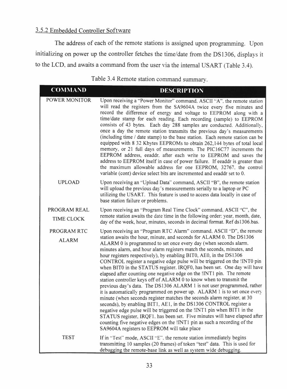
3.5.2 Embedded Controller Software
The address of each of the remote stations is assigned upon programming. Upon
initializing on power up the controller fetches the time/date from the DS1306, displays it
to the LCD, and awaits a command from the user via the internal USART (Table 3.4).
Table 3.4 Remote station command summary.
COM\L\ND
POWER MONITOR
UPLOAD
PROGRAM REAL
TIME CLOCK
PROGRAM RTC
ALARM
TEST
DESCRIPTION
Upon receiving a "Power Monitor" command. ASCII 'A", the remote station will read the registers from the SA9604A twice every five minutes and record the difference of energy and voltage to EEPROM along with a time/date stamp for each reading. Each recording (sample) to EEPROM consists of 43 bytes. Each day 288 samples are conducted. Additionally, once a day the remote station transmits the previous day's measurements (including time / date stamp) to the base station. Each remote station can be equipped with 8 32 Kbytes EEPROMs to obtain 262,144 bytes of total local memory, or 21 full days of measurements. The PIC16C77 increments the EEPROM address, eeaddr. after each write to EEPROM and saves the address to EEPROM itself in case of power failure. If eeaddr is greater than the maximum allowable address for one EEPROM, 32767. the control variable (cont) device select bits are incremented and eeaddr set to 0.
Upon receiving an "Upload Data" command, ASCII "B", the remote station will upload the previous day's measurements serially to a laptop or PC utilizing the USART. This feature is used to access data locally in case of base station failure or problems.
Upon receiving an "Program Real Time Clock" command, ASCII "'C", the remote station awaits the date time in the following order: year, month, date, day of the week, hour, minutes, seconds in decimal format. Ref dsl306.bas.
Upon receiving an "Program RTC Alarm" command. ASCII "D", the remote station awaits the hour, mmute, and seconds for ALARM 0. The DS1306 ALARM 0 is programmed to set once every day (when seconds alarm, minutes alarm, and hour alarm registers match the seconds, minutes, and hour registers respectively), by enabling BITO, AEO, in the DS1306 CONTROL register a negative edge pulse will be triggered on the !INTO pin when BITO in the STATUS register. IRQFO, has been set. One day will have elapsed after coimting one negative edge on the !INT1 pin. The remote station controller keys off of ALARM 0 to know when to transmit the previous day's data. The DS1306 ALARM 1 is not user programmed, rather it is automaticalK programmed on power up. ALARM 1 is to set once even. minute (when seconds register matches the seconds alarm register, at 30 seconds), by enabling BITl, AEl, in the DS1306 CONTROL register a negative edge pulse will be triggered on the !INT1 pin when BIT I in the STATUS register, IRQFl. has been set. Five minutes will have elapsed after coimting five negative edges on the !INT1 pin as such a recording of the SA9604A registers to EEPROM will take place
If in "Test" mode, ASCII "E". the remote station immediately begins transmitting 10 samples (20 fi-ames) of token "test" data. This is used for debugging the remote-base link as well as system wide debugging.
33
Figure 3.4 depicts the expected makeup of the transmitted frames. A "Test"
transmission follows this figure also. First, the station transmits a 9-byte long command
frame. A value of $BB appears in the Command Type byte (data_field[0]) for test
transmissions. The maximum number of fi-ames. the frame maximum, n=20, appears in
bytes data_field[l] and data_field[2] while the rest of the data field is not used for a
command type frame. Next the remote will send one sample (two frames) per second
after acquiring the tune/date from the real-time clock and sending it in the transmitted
samples. The active energy, reactive energy, voltage and frequency portions of the data
field are filled witii $000A, $100A, $200A, $300A respectively where "A" in tiie hex
numbers will be "B" and "C" for phases B and C. respectively. After transmitting the
final fi-ame the remote station program returns and prompts for a further command and
displays the time/date.
3.6 Designed PCBs
Since the design of the remote station and the base station were similar and for the
sake of feasibility and flexibility it was decided only to design two PCBs: generic station
PCB, and transducer PCB. The appendix includes drawings relevant to the PCBs
designed.
The transducer PCB measures 155 mm x 100 mm. Five communications lines.
SCK, DO, DL CS, and F150, are connected to headers so that an inter-board connection
can be made to the PIC16C77 pins.
Since the base station contained a receiver and the remote station a transmitter
only, a generic station board was designed to accommodate either arrangement or both.
All pins that w ere unused from any device (IC) on the board were brought out to headers
on the outer edges of the board. These are knowTi as expansion pins. For a remote
station five connections needed to be accommodated for the SAMES 9604A (SCK, DO.
DL CS. and F150). The pins for these connections were treated as "expansion pins"; as
such they were brought out to headers like other pins. This provides the means to
interconnect the tw o PCBs appropriatel.
34

This concludes the system design. The next chapter offers a look at testing and
implementation of the various subsystems.
35

CHAPTER IV
TESTING
4.1 Introduction
Testing of each individual subsystem was necessary in order to obtain system
design integrity. The EEPROM's. LCD's, RPC-OOO-DIL's, transmitters and receivers
were proven to work m [10]. Subsystems tiiat remained to be tested included the DS1306,
MAX232N with new configuration, and finally tiie SA9604A IC.
4.2 Test of TI MAX232N RS232 Driver
First, the MAX232N"s new optically isolated configuration needed to be tested.
A PIC controller was programmed to receive a byte and send the same byte out the
hardware USART. Originally both the TX and RX (referenced from the PIC side) optical
isolators were biased the same. The collector of the transistors used a 5.6 kQresistor
while the bias resistor for the diode was 1 kD. Testing of this configuration showed the
PIC did not receive the correct bytes or did not receive the bytes at all. A 1 kQ resistor
was used on the collector of the RX channel transistor and this fimctions without fail.
4.3 Test of DS 1306 Real-Tune Clock
Second, the DS1306 was tested utilizing the program DS1306.bas included in the
appendix. The program waits for the ASCII character "C" from the user, via the serial
Visual Basic interface, then accepts the year, month, date, day of week, hour, minute, and
second from the PC. Originally the CE. SCLK, and SDA lines were connected to
PORTC.l, P0RTE.2. and PORTE.l. respectively. While CE high, tiie address of tiie
seconds read register was shifted out on SCLK. The DS1306 first receives the address of
the first register then sends the data out SDA and as long as CE remains high and SCLK
is received an internal counter increments the register pointer automatical!) and the
DS1306 sends the next register's contents, the minutes. Using a digital oscilloscope
SCLK fimctioned on the SHIFTOUT of the seconds read register address. On all
subsequent SHIFTIN's. the clock failed to fimction. No clear explanation was found for
36

this error as simply connecting the DS1306 to different pins, tiie current configuration in
all schematics, solved the problem.
4.4 Test of SAMES 9604A Transducer
Third, several tests on the SAMES 9604A were conducted. The objective of
these tests was to verify, under known load conditions, whether the register readings
concurred with the test set up. A power bench in tiie department of Electrical
Engineering at Texas Tech University provided 3 phase power and loading. The
transformation ratio of the CTs was 1000:1 and the line current per phase was wound 4
times through each CT. This yielded 4 times the line current per-phase. The program
sames.bas was used to acquire data for the tests discussed here. The SAMES 9604A was
tested under six distinct loading conditions summarized in Table 4.1:
Table 4.1 Summary of test setups.
Test Number
1
2
3
4
5
6
Description
Constant Resistive Load
Stepped Resistive Load
3 Phase Voltage Sag Test
Constant Reactive Load (lagging)
Constant Reactive Load (leading)
Constant Parallel Resistive and Reactive (lagging) load
4.4.1 Test 1 Constant Resistive Load
The program sames.bas was used to acquire data from the SA9604A. Table 4.2
depicts the first 10 and last 10 samples of a test to acquire 100 samples.
First, importance was placed on being able to read the frequency registers before
attempting to read and deduce the data from the others due to the frequenc\'s simple
relation to the register value read:
3.5195MHz f =
register value)- 2
37

Table 4.2 Test 1 Partial listing of raw data.
1 sample 1 2 3 4
^ 6
^ % 9 10 91 9: 93 94 95
% 9^ 9« 99 100
Act i te l 0F232F 0F308D
0F3F52 0F4E10
(TSCAE 0FfiB5C 0F7A21 SFUE7
0F9794 0FA640
144C72 145B19 1469CD 147892 14872D 1495F4
i4A493 U B 3 4 3
14C208 I4D099
Reacthel 0056D1 i.«5^11
Oti5"6S 005818 0 0 5 8 5 ' 005 7F5 005851 005866 005990 005 A28 007308
00734D 00731A 007360 O073D5
0074BE
007531 007583 1X175 "0
0075A3
Vob^el E79540 E94C91 EB28DB ED0459 EEE091 F0BB91 F297EB F4743E F64F70 F82BFF SEBAB8 9096ED 927252 944E98 962AEE 98065B 99E297 9BBE3E 9D9A20 9F764D
FieqlMSB b'llOOOOlO b'l 1000000 b'l 1000000 b'l 1000000 b'llOOOOOO
b'l 1000000 b'llOOOOOO b'llOOOOOO
b'llOOOOOO b'llOOOOOO
b'lOOOOOOO b'lOOOOOOO b'lOOOOOOO
b'lOOOOOOO b'lOOOOOOO
b'lOOOOOOO
b'lOOOOOOO b'lOOOOOOO
b'lOOOOOOO b'lOOOOOOO
Freql 74»D 7486
746A 7492
74CX) 7487 7487
7446
7476 7493 7494
74B1 7493
748D 7449
74 7 A
748E 74B9
749D 7483
A d n ^ 0AD9F7 0AE386 UAEEOC 0AF894 0B0326 0B0DA6 0B182E 0B22BD 0B2D43 0B37C4 0E8CB9 0E973D
oEAira 0EAC46 0EB6DO 0EC164
OECHK) 0ED67D
OEEOF? 0EEBg6
R e a c m ^ FF90DF FF9071
FFXFDE FF8F-6 FF8F40
FF8F20
FF8EDD FF8E1A
FF8D3C FFgCD2 FF6C'0
FF6BFF FF6BB9
FF6B66 FF6A7D
FF69D6 FF6967
FF6941
FF6938 FF68E7
Vdtage2
F0AF3A F261Q)
F44529
F628EB
FIOCFF P9F09D F B W E F FDB874
FP9B64 O i T A F
• 9ASB30
9C6F4B 9E5308
A03712 A21AF0
A3FE41
A i E 2 7 B A7C610
A9A9F0 ABSE29
Freq2MSB
b'llOOlOlO b'l 1001010 b'l 1001010
b'l 1001010
b'UOOlOlO b'llOOlOlO b'llOOIOlO
b'llOOlOlO
b'llOOlOlO b'OOOOlOlO
b'lOOOlOlO b'lOOOlOlO b'lOOOIOlO
b'lOOOlOlO b'lOOOlOlO
b'lOOOlOlO b'lOOOlOlO b'lOOOlOlO
b'lOOOlOlO b'lOOOlOlO
Freq^ 7481
^4E0 7479
7495 7444
7480 7486 74E9
74A1 748E 7486
7483 7462
7498 74DF
7493 "488 "438 747C "493
Active3 0FF559
100376
10I2EE 102286
I031FC 10416A 105OF2
10606F
106FE1 107F74
156565
1574Fn 158471
1593DD 1SA367
15B2DE 15C276
15D1DB 15EI69 15F0F2
Reacti\c3 FF7EB7
FF7DDD
FF7D66 FF7D3A
FF7CC2
FF^C22 FF7B61
FF'AEl FF7A54
FF7A4C FF5378
FF536D FF52FD FF5r-A
FF51C1 FT5126
FF50E3 FF506D FF4F":
FF4E95
Vo iuse3
EABCBB EC6FC5
EE4E26
F02BBC F20A1B F3E7BB FSC61B F7A460
F981BA FB6078
929508 94733F
965SC 982F21I 9AODg5
9BEB2A 9DC97D W A 7 2 7
A1853E A362FD
Fra|3MSB b'llOOlOlO b'l 1001000
b'l 1001000 b'l 1001000 b'llOOlOOO
b'l 1001000 b'l 1001000
b'l 1001000 b'llOOlOOO b'l 1001000 b'lOOOlOOO
b'lOOOlOOO b'lOOOlOOO b'lOOOlOOO b'lOOOlOOO
b'lOOOlOOO b'lOOOlOOO b'lOOOlOOO
b'lOOOlOOO b'lOOOlOOO
Fr«3 1 "4C< "481
748A
7468 74% 749? 74A9
''47C "48: "46;-
7446
748F 748A
74B1 747C 748E
746B 7499
"4DF "4.\3
The frequency registers were read 100 times although Table 4.3 only depicts a
few of the samples
Table 4.3 Test 1 frequency measurement results.
sample
1 2 3 4 5
% 97 98 99 100
Phase 1 MSB LSW
b'llOOOOlO 748D b'llOOOOOO 7486 b'llOOOOOO 746A b'llOOOOOO 7492 b'llOOOOOO 74CD b'lOOOOOOO 747A b'lOOOOOOO 748E b'lOOOOOOO 74B9 b'lOOOOOOO 749D b'lOOOOOOO 7483
Mean Standard Deviation
Minimum Maximum
Hex2Dec
29837 29830 29802 29842 29901 29818 29838 29881 29853 29827
Frequeicy
59.98 60.00 60.05 59.97 59.86 60.02 59.98 59.90 59.95 60.00
59.99 0.06 59.82 60.05
MSB
b'llOOlOlO b'llOOlOlO b'llOOlOlO b'llOOlOlO b'llOOlOlO b'lOOOlOlO b'lOOOlOlO b'lOOOlOlO b'lOOOlOlO b'lOOOlOlO
Phase 2 LSW
7481 74E0 7479 7495 7444 "493 7488 7438 747C 7493
Hex2Dec
29825 29920 29817 29845 29764 29843 29832 29752 29820 29843
FrequoKy
mm 59.82 60.02 59.97 60.13 59 97 59.99 60.16 60.02 59.97
59-99 0.09 59.80 60.13
MSB
b'llOOlOlO b'llOOlOOO b11001000 b'llOOlOOO b'llOOlOOO b'lOOOlOOO b'lOOOlOOO b'lOOOlOOO b'lOOOlOOO b'lOOOlOOO
Phase 3 LSW
74C5 7481 748A 7468 7496 748E 746B 7499 74DF 74A3
Hex2Dec
29893 29825 29834 29800 29846 29838 29803 29849 29919 29859
Frequenc
59.87 60.01 59.99 60.06 59.97 59.98 60.05 59.% 59.82 59.94
59.98 0.07 59.80 60.06
LSW Least Significant Wwd
Clearly the frequencies measured concur with the expected line frequencies. The
mean of tiie frequencies is 59.99 Hz, 59.99 Hz, and 59.98 Hz for Phase 1. Phase 2. and
Phase 3 respectively and the standard deviations are 0.06, 0.09, and 0.07. respectively.
The frequencies were successfully read from the SA9604A, as such testing proceeded to
the more complicated voltage, acti\ e energy, and reactive energy per-phase.
38

Table 4,4 shows the voltages to be within reason while measured real and reacti\ e
powers were also acceptable. Of note is a calculated power factor from the data of near
1.00 as would be expected for a purely resistive load.
Table 4.4 Test 1 Calculated data, voltage and energies.
Test 1: Ccmstant Resistive Load Parameters:
Frequency of mains Voltage = Mains cycles between readings = time delay between readings =
60 RMS N-L Voltage Rated = 120 8 RMS Current Rated Max = 33.54
0.1333 Constant for Voltage Calculations = 940000 Constant for Energy- Calculations = 640000
Phase 1 2 3
1(A) 0.350 0.230 0.350
\4 1.40 0.92 1.40
P(W) 168.0 110.4 168.0
sample register
sampl
1 ->
3 4 5
96 9-98 99 100
1 E"9540
2 E94C91 3 EB28DB 4 ED0459 5 EEE091
96 98065B 97 99E297 98 9BBE3E 99 9D9A20 100 9F"64D
Mean
Phase 1 Hex to Dec Delta
151—024
15289489 11 15411419 12 15533145 12 1565505" 12 9963099 12 10085015 12 10206782 12 10328608 12 10450509 12
Standard Deviation Miniminr 1
Maximum
Phase 1 e register Hex2Dec Delta
0056D1 005"!1 005-68 005818 005857 00-4BE 007531 0O"583 007570 oo:5.-\3
.A.\erage
- i - ^ T ^ ^
22289 64 223-6 8-22552 re 22615 63 29886 233 30001 115 30083 82 30064 -19 30115 51
Standard Deviation Minimum Maximum
2465 1930 1726 1912 1709 1916 1-67 1826 1901
Vdtage
107.68 116.74 116.55 116.72 116.53 116. "3 116.59 116.64 116.71
116.54 0.91
107.68 116.74
Phase 2 register Hex to Dec
F0AF3A 15
F2616D 15
"3498
884653 F44529 16008489 F628EB 16132331 F80CFF 16 .\3FE41 10
256255 -4-45-
\5E2-B 108-1419 .\-C610 10995216 A9A9F0 11119088 AB8E29 11
E(Var-s) P(Var) register
0.63 0.86 1.74 0.62 2 30 1.14 0.81 -0.19 0.50
0.79 0.81 -1.36 1.74
4.74 6.45 13.04 4.67 17.26 8.52 6.08 -1.41 3.78
5.90 6.05
-102: 13.04
FF90DF FF9071 FF8FDE FF8F-6 FF8F40 FF69D6 FF6%-FF6941 FF6938 FF68E-02-8D6
»
243049
Delta
111155 123836 123842 123924 123-29 123962 123-9" 123872 123961
Phase 2 He.x2Dec Delta E
-28449 -28559 -28-06 -28810 -28864 -38442 -38553 -38591 -38600 -38681
-110 -147 -104 -54
-167 -111 -38 -9
-81
Voltage
106.43 118.57 118.57 118.65 118.46 118.69 118.53 118.60 118.69
118.44 1.23
106.43 118.65
register
EABCBB
EC6FC5 EE4E26 F02BBC F20A1B 9BEB2A 9DC97D 9F.A-27 .A1853E A362FD
Phase 3 Hex to Dec
15383-59
15495109 156175"4 15739836 15862299 10218282 10340"33 10463015 10585406 10707709
Delta
111370 122465 122262 122463 1 ->->-»-•-'
122451 122282 122391 122303
Phases
Voltage
106.63 11725 117.06 117.25 117.07 117.24 117.08 117.18 117 10
11-03 1.0-
106.63 117.25
(Var-s) P(Vff) register Hex2Dec Delta E<Var-s) P(Var)
FF7EB- -3309--1.09 -8.15 FF7DDD -33315 -1.45 -10.89 FF7D66 -33434 -1.03 -7. 71 FF7D3A -334-'8 -0.53 -4.00 FE-CC2 -33598 -1.65 -12 .37 FF5126 -44-62 -1.10 -8.22 FF50E3 -44829 -0.38 -2 82 FF506D -4494--0.09 -0.67 FF4F- 2 -45198 -O.K) -6.00 FF4E95 -45419
-1.02 -7.66 0.68 5. -230 -17 -0 32 -2
10 26
j \ -'
-218 -119 -44
-120 -155 -6"
-118 -251 -221
-2 15 -1.18 -0.43 -1.19 -1.53 -0.66 -1.1" -2 48 -2.18
-1.23 0,-0 -2 " 5 -0.43
-16.15 -8.82 -3.26 -8.89 -11.48 -4 96 -8.74 -1860 -16 3"
-9.22 5.29
-20.60 -3.26
39

Table 4.4 Continued
samp
1 "> :> 4 ?
96 97 98 99 100
e register
0F232F 0F308D 0F3F52 0F4E10 0F5CAE 1495F4 14A493 14B343 14C208 14D099
Average
Ph Hex2Dec
992047 995469 999250 1003024 1006766 1349108 1352851 1356611 1360392 1364121
Standard E>eviatic» Minimum Maximum
Power Factcx th«a(degrees)
ase 1 Delta
3422 3781 3 " 4 3-42 3783 3-43 3760 3-8I 3^29
E(W-s)
21 52 23.-8 23.73 23.53 23,79 23.54 23.65 23.78 23.45
23.64 0.24
21.52 23.78
P (U") register
0AD9F7 161 40 0AE386 178.33 OAEEOC 178.00 0AF894 176.49 0B0326 178.43 0EC164 176.54 OECBFO 177.34 0ED6-D 17833 OEEOP-175.88 0EEB86
177.29 1.-8
161.40 178.33
0.999 1.91
Hex2Dec
-11159 -13606 716300 :'18996
-2ro: 967012 969-12 9-2413 975095 977798
Phase Delta
2447 2694 2696 2706 2695 2-00 2-01 2682 2-03
-)
E (W-s)
15.39 16.94 16.95 17.02 16.95 16.98 16.99 16.87 POO
16.94 0.16 15.39 1-.02
P(W)
115.41 127,06 127.16 127.63 127.11 127.35 127.39 126.50 127.49
127.03 1.21
115 41 127.63
0.998 3.45
register
0FF559 100376 1012EE 102286 1031FC 15B2DE 15C276 15D1DB 15E169 15F0F2
Phase 3 Hex2Dec
1045849 1049462 1053422 105^414 1061372 1422046 1426038 14299-9 1433961 143^938
Delta
3613 3960 3992 3958 3959 3992 3941 3982 3Q--
E (U'-s)
->2 77
24.90 25 10 24 89 2490 25 10 24.78 25.04 25.01
24.91 0.24 22.72 25.10
P(W)
170.41 186.^8 188.29 186.68 186.73 188.29 185.88 18-.81 187.58
186.80 1.77
170.41 188.29
0.999 2.83
The power profile of Figure 4.1 shows that the per-phase powers were near to the
expected values shown in Table 4.4.
.Acn\ e Power
j ^ « * * ^ ^
* ^ ^ ^ • I • • * — * ^ > • ! • ' » * ^ ^
^V*^""''"^^^^''''''^^'^'''"^
^ ;a -
PkM: 1
I 4 * 10 13 I« 19 r 25 2» 31 .U 37 « «3 « 49 52 55 » 61 >i 6 ri -J W ^ C tS n 91 94 9-
sample aiM.99
Reactive Power
< >
1 4 7 i o i 3 M i 9 r ^ 2 s ; ' 3 4 3 ' « ) 4 3 4 6 « s : s s s s s t s 4 e - " 0 ^ 7 E : ^ s : a s a 9 - 9 4 9-sample nja, 99
Figure 4.1 Test 1 profile of acti\e and reacti\e power.
40

4.4.2 Test 2 Stepped Resistive Load
Figure 4.2 depicts the results of a stepped purely resistive load. This plot shows
that although all phases were assumed to be balance phase 2 at times was not loaded as
the other two phases. This indicated a problem with the testing equipment.
Test 2: Stepped Resistive Load Parameters:
Frequency of mains Voltage = Mains c>cles between readings = time delay between readings =
60 8
0.1333
RMS N-L Voltage Rated = RMS Current Rated Max = Constant for Voltage Calculations = Constant for Energy Calculations =
120 33.54
940000 640000
Step 1 o
3 4 5 6
11(A) 0.350 0.290 0.230 0.170 0.105 0.000
x4 1.40 1.16 0.92 0.68 0.42 0.00
P(W) 168.0 139.2 110.4 81.6 50.4 0.0
Active Power
Figure 4.2 Test 2 stepped resistive load profile.
41

4.4.3 Test 3 Voltage Swell/Sag
Figure 4.3 shows how the 3-phase voltage was swelled then sagged.
Phase 1 Phase 2 Phase 3
Mean Standard Deviation
Minimum Maximum
101.88 25.07 58.73 139.92
150
50
103.41 25.61 59.37 142.06
Voltage
102.11 25 17 58,81 140.55
1 4 7 10 13 16 19 22 25 28 31 34 37 40 43 46 49 52 55 58 61 64 67 70 73 76 79 82 85 88 91 94 97
21 Julv99
sample
Figure 4.3 Test 3 voltage swell/sag profile.
4.4.4 Test 4 Constant Lagging Load
A constant load of 144 VAR (lagging) was desired. Table 4.5 shows tiiat tiie
SA9604A detected 18.98 W (Phase 1), 19.49 W (Phase 2), and 20.51 W (Phase 3). As
such the power factors calculated reflect a small resistive component in the load.
42
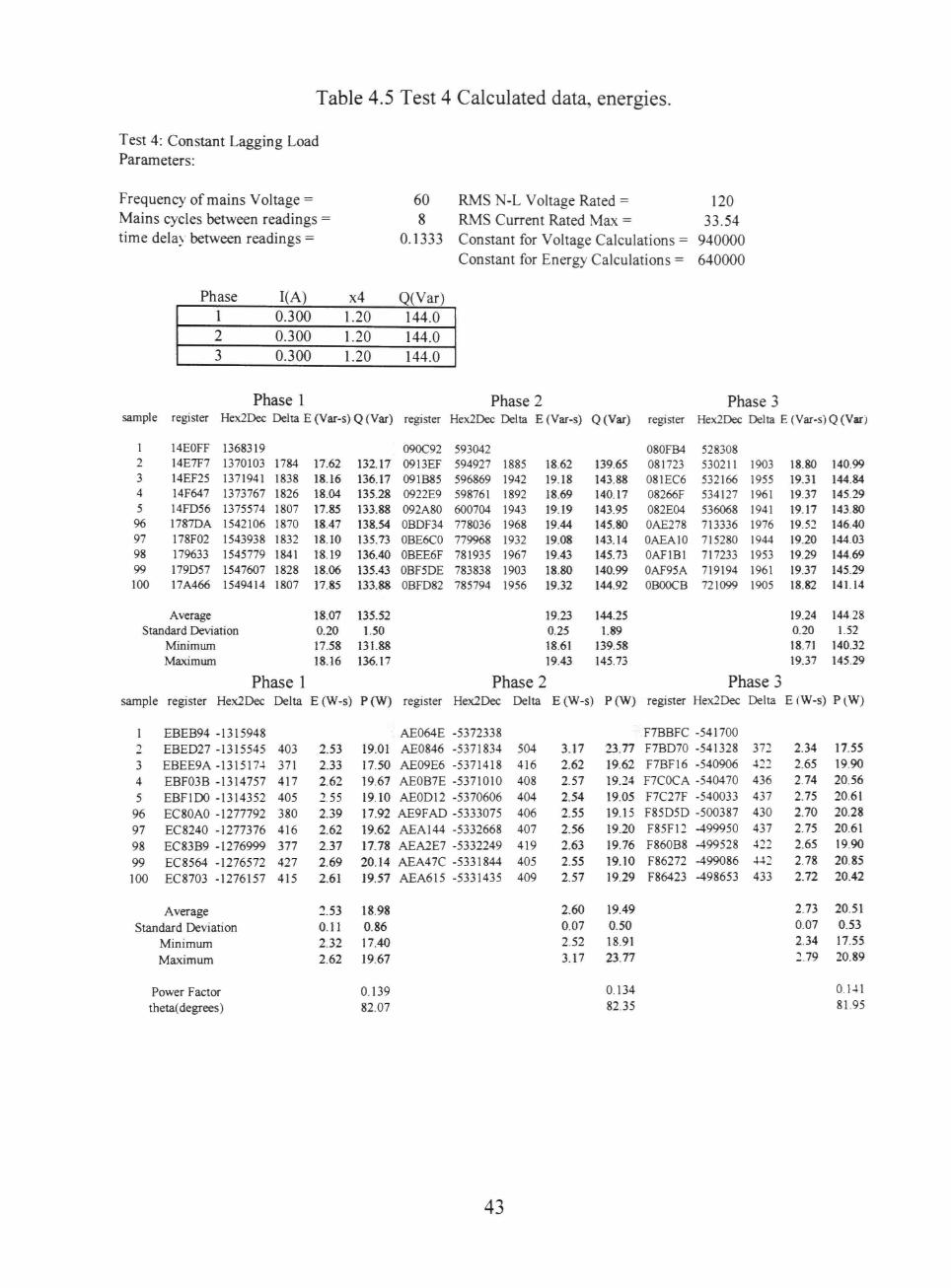
Table 4.5 Test 4 Calculated data, energies.
Test 4: Constant Lagging Load Parameters:
Frequency of mains Voltage = Mains cycles between readings time dela\ between readings =
60 RMS N-L Voltage Rated = 120 8 RMS Current Rated Max = 33.54
0.1333 Constant for Voltage Calculations = 940000 Constant for Energy Calculations = 640000
Phase 1 2 3
1(A) 0.300 0.300 0.300
x4 1.20 1.20 1.20
Q(Var) 144.0 144.0 144.0
Phase 1 Phase 2 sample register Hex2Dec Delta E (Var-s) Q (Var) register Hex2Dec Delta E(Var-s) Q(Var) register
Phase 3 Hex2Dec Delta E (Var-s) Q (Var)
1 2 3 4 5 96 97 98 99 100
14E0FF 14E7F7 14EF25 14F647 14FD56 1787DA 178F02 179633 179D57 17A466
Average
1368319 1370103 1371941 1373767 1375574 1542106 1543938 1545779 1547607 1549414
Standard Deviation Minimum Maximum
1784 1838 1826 1807 1870 1832 1841 1828 1807
17.62 18.16 18.04 17.85 18.47 18.10 18.19 18.06 17.85
18.07 0.20 17.58 18.16
132,17 136.17 135.28 133.88 138.54 135.73 136.40 135.43 133.88
135.52 1.50
131.88 136.17
090C92 0913EF 091B85 0922E9 092A80 0BDF34 0BE6C0 0BEE6F 0BF5DE 0BFD82
593042 594927 596869 598761 600704 778036 779968 781935 783838 785794
1885 1942 1892 1943 1968 1932 1967 1903 1956
18.62 19.18 18.69 19.19 19.44 19.08 19.43 18.80 19.32
19.23 0.25 18.61 19.43
139.65 143.88 140.17 143.95 145.80 143.14 145.73 140.99 144.92
144.25 1.89
139.58 145.73
080FB4 081723 081EC6 08266F 082E04 0AE278 OAEAIO OAFIBI 0AF95A OBOOCB
528308 530211 532166 534127 536068 713336 715280 717233 719194 721099
1903 1955 1961 1941 1976 1944 1953 1961 1905
18.80 19.31 19.37 19.17 19.52 19.20 19.29 19.37 18.82
19.24 0.20 18.71 19.37
140.99 144.84 145.29 143.80 146,40 144,03 144,69 145.29 141.14
14428 1.52
140.32 145.29
Phase 1 Phase 2 Phase sample
rnase i rnase z rnase J register Hex2Dec Delta E (W-s) P(W) register Hex2Dec Delta E(W-s) P(W) register Hex2Dec Delta E(W-s) P(W)
1 EBEB94 -1315948 2 EBED27 -1315545 3 EBEE9A-1315174 4 EBF03B -1314757 5 EBFIDO -1314352
96 EC80A0 -1277792 97 EC8240 -1277376 98 EC83B9 -1276999 99 EC8564 -1276572 100 EC8703 -1276157
Average Standard Deviation
Minimum Maximum
Power Factor theta(degrees)
403 371 417 405 380 416 377 427 415
2.53 2.33 2.62 2.55 2.39 2.62 2.37 2.69 2.61
2.53 0.11 2.32 2.62
19.01 17.50 19.67 19.10
AE064E AE0846 AE09E6 AE0B7E AE0D12
17.92 AE9FAD 19.62 17.78 20.14 19.57
18.98 0.86 17.40 19.67
0.139 82.07
AEA144 AEA2E7 AEA47C AEA615
-5372338 -5371834 -5371418 -5371010 -5370606 -5333075 -5332668 -5332249 -5331844 -5331435
504 416 408 404 406 407 419 405 409
3.17 2.62 2.57 2.54 2.55 2.56 2.63 2.55 2.57
2.60 0.07 2.52 3.17
23.77 19.62 19.24 19.05 19.15 19.20 19.76 19.10 19,29
19.49 0.50 18.91 23.77
0.134 82.35
F7BBFC F7BD70 F7BF16 F7C0CA F7C27F F85D5D F85F12 F860B8 F86272 F86423
-541700 -541328 -540906 -540470 -540033 -500387 -499950 -499528 -499086 -498653
372 422 436 437 430 437 422 442 433
2.34 2.65 2,74 2.75 2.70 2.75 2.65 278 2.72
2.73 0.07 2.34 2.79
17.55 19.90 20.56 20.61 20.28 20.61 19.90 20.85 20.42
20.51 0.53 17.55 20,89
0,141 81,95
43

4.4.5 Test 5 Constant Leading Load
A constant leading load of approximately 163.2 VAR was connected and metered
with the results summarized in Table 4.6.
Table 4.6 Test 5 Calculated data, energies.
Test 5: Constant Leading Load Parameters:
Frequenc) of mains Voltage = Mains cycles between readings = time delay between readings =
60 RMS N-L Voltage Rated = 8 RMS Current Rated Max =
0.1333 Constant for Voltage Calculations = Constant for Energv- Calculations =
120 33.54
940000 640000
Phase 1 2 3
1(A) 0.340 0.340 0.340
x4 1.36 1.36 1.36
Q(Var) 163.2 163.2 163.2
Phase 1 Phase 2 Phase 3 sample registw Hex2Dec Ddta E (Var-s) Q (Va-) register Hex2Dec Ddta E (Var-s) Q(Var) registo- Hex2Dec Delta E (Var-s) Q (Var)
1 2 ^ 4 5
96 9" 98 99 100
19C169 19BA99 19B3AF 19AC0E 19A473 16E"AD 16DFF6 16D84B 16D086 16C8B6
Average
1687913 1686169 1684399 1682446 1680499 1501101 1499126 1497163 14951-4 14931-4
Standard Deviation
impl
1 -> 1 J
4 5
96 97 98 99 100
Minimum Maximum
e register
EF8913 EF88F7
EF88F1 EF890C EF88FA EF893F EF8964
EF893B EF894D EF8953
Average
-1"'44 -1770 -1953 -1947 -1968 -1975 -1963 -1989 -2000
Phase 1 Hex2Dec
-1079021 -1079049 -1079055 -1079028 -1079046 -1078977 -1078940 -1078981 -1078963 -1078957
Standard Deviation Minimum Ma.ximum
Delta
-28 -6 2?
-18 -26 37 -41
18 6
-1-.23 -17,48 -19.29 -19 23 -19.44 -19.51 -19.39 -19.65 -19.76
-19.43 0.33
-19.84 -17,23
E (W-s
-0.18 -0.04 0.17 -0.11 -0.16 0.23 -0,26 0.11 0.04
0.00 0.12 -0.26 0.17
-12921 -131.13 -144.69 -144.25 -145.80 -146.32 -145.43 -147.36 -148.18
-145.73 2.51
-148.77 -129,21
) P ( W )
-1.32 -0.28 1.27
-0.85 -1.23 1,75
-1.93 0.85 0.28
0.03 0.87 -1.93 127
09406B 093925 0931E3 0929F2 0922 IC 06511B 06492C 064143 063947 063169
register
B160AC B16133 B1619D B161EA B16234 B17D04 B17D4A B17D9A B17DE9 B17E35
606315 604453 -1862 602595 -1858 600562 -2033 598556 -2006 4139-9 -: 411948 -: 409923 -:
036 031 025
40^8-9 -2044 405865 -2014
Phase Hex2Dec
-5152596 -5152461 -5152355 -5152278 -5152204 -5145340 -5145270
-5145190 -5145111 -5145035
-18.39 -18.35 -20.08 -19.82 -20.11 -20,06 -20,00 -20.19 -19.89
-20.00 0J27
-20.36 -18.35
2
-137.95 -137.65 -150.62 -148.62 -150.84 -150.47 -150.03 -151.43 -149.21
-150.01 2.00
-152.69 -137.65
Delta E(W-s) P ( W )
135 106 77 74 87 70 80 79 76
0.85 0.67 0.48 0.47 0.55 0.44 0.50 0.50 0.48
0.48 0.06 0.38 0.85
6.37 5 0 0 3.63 3.49 4.10 3.30 3,77 3,73 3.58
3 6 0 0-42 2.88 6.37
03F32D 03EC1D 03E4BF 03DCCE 03D4C2 00FB93 00F394 00EB85 00E395 00DB89
register
FA9E4C FA9E25 FA9E56 FA9E7C FA9E86 F.\A7C6 FAA7E8 F.\.-\804
FAA823 FAA83B
258861 25-053 25516-253134 251074 64403 62356 60293 58261 56201
-1808 -1886 -2033 -2060 -2036 -2047 -2063 -2032 -2060
-17.86 -18.63 -20.08 -20.35 -20,11 -20 22 -20,38 -20.0--20,35
-20 22 0,32
-20,80 -P ,86
Phase 3 Hex2Dec
-352692 -352731 -352682 -352644 -352634 -350266 -350232 -350204 -350173 -350149
Delta
-39 49 38 10 20 34 28 31 24
E(W-s
-0.25 0,31 0,24 0.06 0.13 0.21 0.18 0.19 0.15
0.16 0.07 -0.25 0.31
-133,95 -139,73 -150.62 -152.62 -150.84 -151.66 -15284 -150.55 -152.62
-151.66 2.40
-156.03 -133 95
) P (W)
-1.84 2.31 1.79 0.47 0.94 1.60 1,32 1.46 1.13
1.21 0.56 -1.84 2 3 1
44

4.4.6 Test 6 Constant Parallel Resistive and Lagging Load
A constant parallel resistive and lagging load was desired. Table 4.7 shows the
calculated results while Figure 4.4 illustrates the power profile.
Table 4.7 Test 6 Calculated data, energies.
Test 6: Constant Parallel Resisti\ e and Lagging Load Parameters:
Frequenc of mains Voltage = Mains c\ cles between readings time delay between readings =
60 RMS N-L Voltage Rated = 8 RMS Current Rated Max =
0.1333 Constant for Voltage Calculations = Constant for Energy Calculations =
120 33.54
940000 640000
phase 1 2 3
I(R) 0.35 0.23 0.35
x4 1.4
0.92 1.4
I(L) 0.300 0.300 0.300
x4 1.2 1.2 1.2
P(W) 168
110.4 168
CKVar) 144 144 144
Phase 1 Phase 2 Phase 3 sample register Hex2Dec Ddta E (Vffl--s) Q (Var) regista- Hex2Dec Delta E(V»-s) Q(Var) regista" Hex2Dec Ddta E (Var-s) Q (Var)
1 2 j»
4 5
96 97 98 99 100
DEB312 -2182382 DEB871 -2181007 DEBEEE -2179346 DEC56C -2177684 DECC4E -2175922 E11D97 -2024041 El2414 -2022380 E12A9C -2020708 E1313C -2019012 E1384F -2017201
.•\\eraee Standard Deviatiai
Minimum Maximum
1375 1661 1662 1762 1652 1661 1672 16% 1811
Phase 1 imple regista- Hex2Dec
1 2 _
4 5
96 97 98 99 100
B7CE3A -4731334 B7DC05 -4727803 B7E9EB -4724245 B7F8B1 -4720463 B807C7 -4716601 BD6721 -4364511 BD764B -4360629 BD856E -4356754 BD9463 -4352925 BDA392 -4349038
Average Standard Deviation
Minimum Maximum
Power Factor theta
Delta
3531 3558 3782 3862 3852 3882 3875 3829 3887
13.58 16.41 16.42 17.41 16.32 16.41 16.52 16.75 17.89
16.48 0.91 13.58 18.91
E (W-s)
22 21 22.38 23.78 24.29 24.22 24.41 24.37 24,08 24,44
24.28 0.31 22 21 24.32
101.87 123.% 123.13 13054 122 39 123,(^ 123,87 125.65 134 17
123 61 6.82
101.87 141.«)
P (W)
D06DA6 D07439 D07AD4 D08262 D08A2F D3409B D347F1 D34F80 D35703
D35EDD
r a s t e r
43F0BE 166.54 43FAFF 167.82 178,38 182.15 181.68 183.10 182.77 180.60 183.33
182.13 2.30
166.54 182,44
0.827 34,2
44049B 440FD9 441AF9 481241 481D65 48288D 4833BB 483EE0
-3117658 -3115975 -3114284 -3112350 -3110353 -2932581 -2930703 -2928768 -2926845 -2924835
1683 1691 1934 1997 1814 1878 1935 1923 2010
Phase 2 Hex2Dec
4452542 4455167 4457627 4460505 4463353 4723265 4726117 4728973 4731835 4734688
Delta
2625 2460 2878 2848 2851 2852 2856 2862 2853
16.63 16.70 19.10 19.73 17.92 18.55 19.11 19.00 1 9 . ^
19.24 1.06 16.63 21.06
E(W-s)
16.51 15.47 18.10 17.91 17.93 17.94 17.96 18.00 17.94
1792 0.29 15.47 18.10
124.69 125 28 143.29 147.95 134.39 139.14 143.36 142.47 148.92
144.30 7.93
124.69 157.95
POV)
123.81
C6F612 C6FC63 C''0313 C70A8B C-129B
C9AC2D C9B3B1 C9BB82 C9C3C9 C9CB1E
r a s t e r
CF44EC CF5301
116 03 CF61AB 135.74 134.33
CF7153 CF8167
134.47 D53A0E i:>4 52 D54A2F 134.71 D55A39 134.99 D56A5D 134.56 D57A7A
134,42 2.18
116,03 135.74
0.682 47.1
-3738094 -3736477 -3734765 -3732853 -3730789 -3560403 -3558479 -3556478 -3554359 -3552482
1617 1712 1912 2064 1866 1924 2001 2119 1 8 "
Phase 3 He\2Dec
-3193620 -3190015 -3186261 -3182253 -3178137 -2803186 -279905" -2794951 -2790819 -2786694
Delta
3605 3754 4008 4116 4116 4129 4106 4132 4125
15.97 16.91 18.89 20.39 18.43 19.01 1977 20.93 18.54
18.52 1,04 15.97 20.39
E(W-s)
22,67 23.61 25 21 25.88 25.88 25.97 25 82 2599 25.94
25.85
0.41 22.67 25.88
119.«) 126,84 141.66 152.92 138.25 142.54 148.25 156.99 139.06
138,90 7.79
119.80 152.92
P(W)
170.03 177.06 189.04 194.13 194,13 194,75 193.66 194.89 194.56
193,87
3,07 170.03 194.13
0.813
35.6
45

150
PtlMCl
- • - P f c « e 2
^ ^ P b « K 3
!
' ^ 1 100 '
0
* 7 10 13 16 19 22 25 2» 31 J4 37 4. 43 46 49 52 55 58 61 64 67 70 73 76 79 »2 15 M 91 5~i 97
Hmpk 21 Ial)r99
Reactive Poner
2S0
150
1 100
50
M^^^^^^^^^m^ P l n n l
1 r\mw. T
» PIIMI3
1 4 7 10 13 16 19 2 2 2 S 2 8 3 1 3 4 3 7 « ) 4 3 4 6 « 5 2 5 5 S 8 6 1 6 4 6 7 7 0 7 3 7 8 7 9
sample
88 91 94 97
Figure 4.4 Test 6 profile of active and reactive power.
All six tests performed on the SA9604A show the device provides accurate data
for both constant resistive and reactive loads as well as varying loads.
The communications and data transfer aspect of this power monitoring system
successfiilly achieves the objectives of the design. Extensive testing of a Go-Back-N
ARQ protocol utilizmg the same system design was conducted in [10]. As such the
digital communications portion of the design fimctions well. Frequency, voltage, active
and reactive energy measurements are now available using the SA9604A. Time/date
information is readily available using the DS1306. Thus all system sub components have
been tested utilizmg the programs appended to this thesis with the prototyping problems
as noted earlier in the chapter. Other problems experienced during testing are
documented in [10].
This thesis concludes with a look at cost and recommendations.
46

CHAPTER V
CONCLUSION
5.1 Introduction
To conclude this thesis the costs of the system, the designed PCBs, and the
flexibility of the design will be presented.
5.2 Project Cost Summary
5.2.1 Total Cost of Remote and Base Station
Table 5.1 illustrates the costs of one remote station and one base station. These
costs do not reflect actual development expenses as some devices were acquired fi*ee of
charge. Table 5.1 also does not consider the cost of the Microchip PicStart Plus eprom
programmer or a UV eprom lamp.
Table 5.1 Cost of one remote and base station.
ITEM
Base Station
Remote Station w/ transducer
TOTAL COST
Price
$120.87
$124.39
$245.26
5.2.2 Cost Breakdovm of Base Station
The cost breakdown for an individual base station is depicted in Table 5.2. The
suppliers mentioned in Table 5.2 offered the best possible price for the listed device. In
some cases, lower prices may be obtained by ordering greater quantities.
47

Table 5.2 Base station cost simimary.
ITEM
Microchip PIC16C77/JW
Microchip 24LC256-I/P EEPROM
Radiometrix RX2-433-F-5V
Whip antennas 433.92 MHz
Radiometrix RPC-DIL-000
Optrex DMC-16249B (LCD)
Texas Instruments MAX232N
NEC PS2501-2 Opto-Isolator
DS1306 Real-Time Clock
FOXNC38 32.768 KHz
FOX200 20.0 MHz
FOXlOO 10.0 MHz
Various
TOTAL BASE STATION
Supplier Qt> I nit Price
Digikey
Digikey 1
Lemos, Int.
Lemos, Int.
Lemos, Int.
Digikey ]
Allied ]
Mouser
Insight
Mouser
Mouser
Mouser
-
-
[ $15.70
I $2.55
I $43.30
-
[ $8.00
[ $16.62
I $1.04
[ $0.55
I $3.31
I $0.33
I $0.86
I $0.76
$10.00
-
Subtotal
$15.70
$36.10
$79.40
$79.40
$87.40
$104.02
$105.06
$105.61
$108.92
$109.25
$110.11
110.87
$120.87
$120.87
5.2.3 Cost Breakdovm of Remote Station
Table 5.3 illustrates the cost of one remote station.
As compared to the design of the remote power monitoring system in [10] a
significant increase in features is seen in this design while the costs were reduced. This is
due in part to the fact that the system now communicates in one single direction and to
the procxirement of cheaper devices. Although the system designed and presented here is
one of a imi-directional communications system the design welcomes a plethora of
changes that increase its potential.
48

Table 5.3 Remote station cost summary.
ITEM
Microchip PIC 16C77/JW
Microchip 24LC256-I/P EEPROM
Radiometrix TX2-433-5V
Whip antennas 433.92 MHz
Radiometrix RPC-DIL-000
Optrex DMC-16249B (LCD)
Texas Instruments MAX232N
NEC PS2501-2 Opto-Isolator
DS1306 Real-Time Clock
FOXNC38 32.768 KHz
FOX200 20.0 MHz
FOXlOO 10.0 MHz
SAMES 9604A
FOX036S
Various
TOTAL REMOTE STATION
Supplier Qt\ I nit Price
Digikey
Digikey J
Lemos, Int.
Lemos, Int.
Lemos, Int.
Digikey
Allied ]
Mouser
Insight
Mouser
Mouser
Mouser
SAMES ]
Mouser
-
-
[ $15.70
I $2.55
I $26.32
I $0.00
I $8.00
I $16.62
I $1.04
I $0.55
I $3.31
I $0.33
I $0.86
I $0.76
I $20.06
I $0.44
$10.00
-
Subtotal
$15.70
$36.10
$62.42
$62.42
$70.42
$87.04
$88.08
$88.63
$91.94
$92.27
$93.13
$93.89
$113.95
S114.39
$124.39
$124.39
5.3 Flexibihty of the Design
The PCBs designed are designed to welcome changes that allow system
improvement. One such improvement the design accommodates is the insertion of both
transmitters and receivers for bi-directional communication. \Vlth bi-directional
commxmication a control feature is introduced into the system. Data could be requested
b> the base station and a retransmission technique employed, using the same fi-ame
structure and definitions designed here, to insure that data is received properly. The uni
directional design suffers in that if a data packet is lost the only wa> to recover this data
is to do it localh with a laptop connected to the remote station DB-9 serial interface. A
bi-directional feature would solve this problem through the proper protocol such as ARQ
or Go-back-N. Bi-directionality also would allow the remote stations to recei\e
49

commands such as to turn on automatic capacitor banks or filters in the event of a low
power factor or harmonic distortion.
Another feature is that both antenna outputs are a\ailable meaning a gain
amplifier could be designed on a separate board to mcrease the range of the stations.
This is recommended due to the presence of EM radiation near transformers and power
lines.
The base station contains 11 expansion pins while each remote contains 6. These
expansion pins could be used to send/receive signals to/fi-om other devices such as
detecting when !INTO and !INT1 are asserted by tiie DS1306 real-time clock. The use of
the expansion pins in a control system is limitless.
The SPI bus of the SA9604A is a tri-state bus, as such multiple metering IC"s
could be connected to the same bus while expansion pins could be used as de\ice enable
control lines. This feature is usefiil where multiple transformers may be connected at the
same site requiring onl\' one remote station to acquire measurements fi-om all metering
IC"s. The proper firmware should be developed to accommodate this type of system.
The presentation of a flexible "Digital Wireless Power Metering System" is now
complete. Justification, technical design over\iew, testing and conclusions ha\e been
covered. The appendix includes schematics for a uni-directional system as well as the
programs developed for this system. Schematics for a bi-directional setup as w ell as the
first page of the data sheets for most devices are included for reference.
The author wishes to thank all those who contributed to this project and is
available for comments or suggestions via email at the following electronic mail address:
50

REFERENCES
1] Llamas, Armando Ph.D., ET. Al. Sistema de Monitoreo de Potencias Real >' Reactiva en Localidades Multiples. Memorias de la XXV Reunion de Investigacion \ DesarroUo Tecnologico del Sistema I.T.E.S.M., Tomo II. pp. 33-343. Jan. 1995.
2] Goldie, John. Summary of well known interface standards. National Semiconductor Application Note 216. Jan. 1995.
3] Llamas, Armando Ph.D. and A Tejada. Aplicaciones del Sistema de Monitoreo de Potencias Real y Reactiva en el I.T.E.S.M.. I Simposio de Ciencia y Tecnologia, Monterrey 400. Jan. 1995.
4] Keiser, Gerd E. Local Area Networks. New York: McGraw-Hill Book Company 1989.
5] FOX Literature Oscillator Theors of Operation. FOX Electronics Inc. Florida: 1998.
6] Microchip Literature. DS21203F. Microchip Technology Inc. Chandler, Arizona 1997.
7] Radiometrix Literature. RPC Data Sheet. Radiometrix Ltd. Hertfordshire, England. Feb. 1998.
8] Parzen, Benjamin. Design of Crystal and Other Harmonic Oscillators. New York: John Wiley & Sons. 1983.
9] SAMES Literature. 7190. PDSQ39-SA9604A-Q01 REV. C. SAMES (Pty) Ltd. 1998.
10] Pmeda, Adrian Amoldo Davila. Go-Back-N ARQ Multiple Station Digital Wireless Power Monitoring Svstem Design. I.T.E.S.M. Monterrey. N. L. Mexico. May 1999.
51

APPENDIX
File sysdef.bas -Autbor A. I*ineda
' Project Multiple Staticm EHgital \^'ireless Power Metering System
This file defines the port/pin assignments and otfier harware setups necessai% for the s> stem The following line of code must be the first line of code on any program wishing to use these definitions.
Include 's>sdef has"
Include "modedefe.bas" ' Include shift modes
' Definitions fw PIC hardware setup
DEFINE OSC 20 ' 20 MHz. oscillator speed DEFINE HSER_RCST\ 90h ' USART Receive mode DEFIN'E HSER_TXST\ 20h ' LS.\RT Transmit mode DEFINT HSER BAUD 9600 ' USART baud rate
' Definitions for LCD display
DEFCSE LCD_EREG PORTE DEFINT LCD EBIT 0
' Definitions for EEPROMS
DPIN var PORTD.O ' D C data pin CPIN var PORTD.l HC clock pin
cont var bMe
T)efinitions for RPC chip
.ASM RPC TX.-V TXR RX-A RXR END-ASM
D3 02 Dl DO TXA. TXR RX.^ RXR
RST
t
var var var var var var var var
var
EQU EQU EQU EQU EQU
PORTB. 7 PORTB.6 PORTB.5 PORTB 4 PORTB.3 PORTB2 PORTB. 1 PORTB.O
PORTD.7
TtefinitiOTS for S.AMES 9604.A
SCK DO Dl
var var var
PORTC3 PORTC.5 PORTC.4
06 3 2 I 0
52

cs F150
t
var var
P0RTD.3 PORTD.2
'Definitions for Clock
CE SCLK SDA
day date month year hour minute second
var var var
PORTD.6 PORTD.5 PORTD.4
var byte var byte var b\te \ar byte var b\te \ar b\te var bMe
secad con $00
secalrmO con $07 secalrml con $0B
minad con $01 hourad con $02 dayad con $03 datead con $04 monthad con $05 > earad con $06 ctriad con$0F wr con $80
53

' File: sames.bas ' Author A. Pineda ' Project: Multiple Staticm Digital W ireless Power Metering System
'Program to read the all Registers of the S.\MES %04A ' Program sends data out the hardware USART, end of transmission is signaled b% "EOF" ' The registers are read by comparing bits 18 and 19 of fi^uency A register, wtien bits ' are equal this will signifj a measurement c> cle is complete, 133ms approx.
'Status: It works 12/99!!!
Include "svsdef bas" ' Include s\stem definiticms
temp temp2 n
PI Al PI .A2 PI .\3 PI Rl PI R2 PI R3 PI VI PI \"2 PI V3 PI fl PI n P1_G
P2 Al P2 .A2 P2 A3 P2 Rl P2 R2 P2 R3 P2 VI P2 V2 P2 V3 P2 fl P2 £2 P2_G
P3 Al P3 -M P3 .A3 P3 Rl P3 R2 P3 R3 P3 VI P3 \ 2 P3 \'3 P3 fl P3 f2 P3_G 1
var var var
var var var var var var var var var var var var
var var var var var var var var var var var var
var var var var var var var var var var var var
b>te b\te b\-te
byte b>te b\te b\te b\te b\te b\-te b>te byte b\T:e b\te byte
byte byte byte byte b>te b>te b\te b>te b>te b>te b>te b\te
b>te b>te byte byte b>te byte b\te b\te b\te b\te b>te byte
high PORTC.O
low c s
pause 500
LCDOLT $fe. 1. "enter g" ' Wait for "g" from Visual Basic
v»-ait: HSERIN [temp] if temp != "g" then wait
highCS
54

Shiftout DO, SCK. MSBFIRST, [%110000011\9] ' Get first byte of frequency I register Shiftin Dl, SCK, MSBPOST, [temp] ' saved as temp lowCS
forn= 1 to 100
testit: highCS
Shiftout DO, SCK, MSBFIRST, [%110000011\9] ' Here wait until bits equal, to those in temp Shiftin DL SCK, MSBPOST, [temp2] lowCS
if temp2.2 = temp.2 and temp2.3 = temp.3 then acquire ffotn te<;tit goto testit
acquire: ' ok then take reading LCDOUT $fe,l. dec n toggle PORTCO '** used for testing
highCS Shiftout DO, SCK, MSBFIRST, [%110000000\9] ' send address of first register only, keep CS high Shiftin Dl, SCK, MSBPOST, [Pl_AI,PI_A2,Pl_A3,Pl_RI.Pl_R2,Pl_R3,Pl_Vl,Pl_V2,Pl_V3,Pl_fl,Pl_f2,Pl_G] Shiftin Dl, SCK, MSBPOST, [P2_Al,P2_A2,P2_A3,P2_Rl,P2_R2,P2_R3,P2_Vl,P2_V2,P2_V3,P2_fl.P2_f2,P2_G] Shiftin Dl, SCK, MSBPOST, [P3_Al,P3_A2,P3_A3,P3_Rl,P3_R2,P3_R3,P3_Vl,P3_V2,P3_V3,P3_fl,P3_f2,P3_f3] lowCS
HSEROUT [hex2 Pl_Al,hex2 Pl_A2,hex2 PI_A3, tab] HSEROUT [hex2 PI_Rl.he\2 PI_R2,hex2 P1_R3, tab] HSEROUT [hex2 Pl_Vl,hex2 Pl_V2,hex2 P1_V3, tab] HSEROUT ["b'",bin8 Pl_fl,tab,hex2 Pl_f2,hex2 Pl_f3, tab]
HSEROUT [hex2 P2_Al,hex2 P2_A2,hex2 P2_A3, tab] HSEROUT [hex2 P2_RI4iex2 P2_R2,hex2 P2_R3, tab] HSEROUT [hex2 P2_VI,hex2 P2_V2,hex2 P2_V3, tab] HSEROUT ["b'",bin8 P2_fl,tab, hex2 P2_f2,hex2 P2_f3, tab]
HSEROUT [hex2 P3_Al,hex2 P3_A2,hex2 P3_A3, tab] HSEROUT [hex2 P3_Rl,hex2 P3_R2,hex2 P3_R3, tab] HSEROUT [hex2 P3_VI,hex2 P3_V2,hex2 P3_V3. tab] HSEROUT ["b"',bin8 P3_fl,tab, hex2 P3_f2,hex2 P3_f3, cr]
next n
HSEROUT ["EOF"] ' for Visual Basic
LCDOUT $fe,l, "DONE"
End
55

' File: dsl306.bas ' Author: A. Pineda ' Project: Multiple Station Digital U ireless Power Metering S\stem
'Itworks! 6/28/99
'Program accepts program time from PC in decimal format and programs the clock accordingly ' Continually displays time on LCD and sends out USART for debugging with H\per-terminal.
Include "sysdef bas"
temp var byte temp2 var byte
GOTO START
' Subroutine to convert from Decimal to BCD
C0NVERT2BCD: temp2 = temp DIG 0 ' Save one's digit temp = temp DIG 1 ' Save ten's digit temp = temp « 4 ' Shift 4 to left x 16 temp = temp + temp2 ' Add results (now in BCD) return
START: LCDOUT $fe,l ' Second..Wait for ascii "G" LCDOUT "Enter 'G'"
wait: HSERIN [temp] if temp != "G" then wait
HSERIN [dec2 temp] ' Receive Year GOSUB C0NVERT2BCD:year = temp
HSERIN [dec2 temp] ' Receive Month GOSUB CONVERT2BCD:montii = temp
HSERIN [dec2 temp] ' Receive Date GOSUB C0NVERT2BCD:date = temp
HSERIN [dec2 temp] ' Receive Da\ of week GOSUB CONVERT2BCD:day = temp
HSERIN [dec2 temp] ' Receive Hour GOSUB CONVERT2BCD:hour = temp
HSERIN [dec2 temp] ' Receive Minutes GOSUB C0NVERT2BCD:minute = temp
HSERIN [dec2 temp] ' Receive Seconds GOSUB CONVERT2BCD:second = temp
LCDOUT $fe,l LCDOUT "Programming" pause 500
HSEROUT [hex date."r,hex month,"/".hex year," ",hex day," ".hex hour,":".hex minute,":",hex second," EOF"]
' First.. Upon initial power up, the state of the \\T bit in the CONTROL register is undefined there WT should be cleared on start up.
high CE ' select device shiftout SDA,SCLK,lsbfirst,[$8F,%00000000] ' enable write low CE ' deselect device
high CE ' select device
56

shiftout SDA,SCLK,lsbfirst,[$8F,%00000100] ' enable IHz out low CE ' deselect device
high CE ' select device shiftout SDA,SCLK,lsbfirst,[secad-rwr] ' Send seconds address shiftout SDA,SCLK,lsbfirst, [second] ' Program Seconds shiftout SDA,SCLK,lsbfirst, [minute] ' Program Minutes shiftout SDA,SCLK,,lsbfirst,[hour] ' Program Hour shiftout SDA,SCLK,lsbfirst,[day] • Program Day shiftout SDA,SCLK,lsbfirst,[date] ' Program Date shiftout SDA,SCLK,Isbfirst, [month] ' Program Month shiftout SDA,SCLK,lsbfirst,[year] ' Program Year low CE ' deselect de\ ice
' Now loop reading the time and sending it to display and USART for debugging
loop: highCE shiftout SDA,SCLK,lsbfirst, [secad] ' send seconds address shiftin SDA,SCLK,msbfirst,[second,minute,hour,day,date,month.Near] low CE
if day = 1 then LCDOUT $fe,l,"M"
endif if day = 2 then
LCDOUT Sfe.I, "Tu" endif if day = 3 then
LCDOUT Sfe. 1,''W" endif if day = 4 then
LCDOUT $fe,l,"Th" endif if day = 5 then
LCDOUT $fe,l,"F" endif if day = 6 then
LCDOUT $fe,l, "Sa" endif if day = 7 then
LCDOUT $fe,l,"Su" endif
LCDOUT hex2 date,"/"Jiex2 month,"/"Jiex2 \ear." ",hex2 hour."h".hex2 minute,"m",hex2 second,"s"
HSEROUT [hex2 date,"/".hex2 month."/",hex2 \ear." ",hex2 hour,"h"4iex2 minute, "m",hex2 second,"s"] HSEROUT [cr]
goto loop
57

File: difference.bas Author: A. Pineda Project: Multiple Station Digital V\ ireless Power Metering System
Program to read the all Registers of the SAMES 9604A Program sends data out tiie hardware USART, end of transmission is signaled by "EOF" The registers are read b\ comparing bits 18 and 19 of frequency A register, when bits are equal this will signify a measurement c\cle is complete, 133ms approx.
Two readings are taken and the difference (delta n) is calculated.
Status: It works 8/7/99!!!
Include "sysdef bas" ' Include system defmitions
temp temp2 n i
PIB P2B P3B PB
PIA P2A P3A PA
PC 1
var var var var
var var var var
var var var var
var
byte b\ie b\te byte
byte[12] byte[12] byte[I2] word
byte[I2] byte[12] b>te[12] word
word
start:
high PORTCO
lowCS
pause 500
LCDOUT $fe, 1, "enter "B'" ' ^ ait for "B" from Visual Basic
wait: HSERIN [temp] if temp != "B" then wait
highCS Shiftout DO, SCK. MSBFIRST, [%110000011\9] ' Get first bvte of frequency 1 register Shiftin DL SCK, MSBPOST, [temp] ' saved as temp
low CS
pause 40
HSEROUT["000L"]
forn = l to 100
testit: high CS
Shiftout DO, SCK, MSBFIRST, [%110000011\9] ' Here wait until bits equal, to tiiose in temp Shiftin DL SCK, MSBPOST. [temp2]
lowCS
if temp2.2 = temp.2 and temp2.3 = temp.3 then acquire goto testit
acquire: ' ok then take reading LCDOUT $fe,l, dec n
58

toggle PORTC.O '** used for testing
highCS Shiftout DO, SCK, MSBFIRST, [%110000000\9] ' send address of first register only, keep CS high Shiftin Dl SCK, MSBPOST. [P1B[0],P1B[I],P1B[2],P1B[3],P1B[4],P1B[5],P1B[6],P1B[7],PIB[8],P1B[9],P1B[10],P1B[11]] Shiftin DL SCK, MSBPOST, [P2B[0],P2B[1],P2B[2],P2B[3],P2B[4],P2B[5],P2B[6],P2B[7],P2B[8],P2B[9],P2B[10],P2B[11]] Shiftin DL SCK, MSBPOST, [P3B[0],P3B[1],P3B[2],P3B[3],P3B[4],P3B[5],P3B[6],P3B[7],P3B[8],P3B[9],P3B[10],P3B[11]]
lowCS
pause 50
testit2: highCS
Shiftout DO, SCK, MSBFIRST. [%I lOOOOOl 1\9] ' Here wait until bits equal, to tiiose in temp Shiftin Dl, SCK, MSBPOST. [temp2]
lowCS
if temp2.2 = temp.2 and temp2.3 = temp.3 then acquire2 goto testit2
acquire2: ' ok then take reading LCIXDUT$fe,l,decn toggle PORTC.O '** used for testing
highCS Shiftout IX), SCK, MSBFIRST, [%110000000\9] ' send address of first register only, keep CS high Shiftin DL SCK, MSBPOST. [P1A[0],P1A[1],P1A[2],P1A[3],PIA[4],PIA[5],P1A[6],PIA[7].P1A[8],P1A[9],P1A[10],P1A[11]] Shiftin DL SCK, MSBPOST. [P2A[0],P2A[1],P2A[2],P2A[3],P2A[4],P2A[5],P2A[6],P2A[7],P2A[8],P2A[9],P2A[10],P2A[11]] Shiftin Dl, SCK, MSBPOST. [P3A[0],P3A[1],P3A[2],P3A[3],P3A[4],P3A[5],P3A[6],P3A[7],P3A[8],P3A[9],P3A[10],P3A[11]]
lowCS
for i = 1 to 4
REAL 1 PA.lowbyte =PlA[i+l] PA.highbyte = PIA[i]
PB.lowbyte =PIB[i+I] PB.highbyte = PlB[i]
PC = PA - PB
PlA[i] =PC.highbyte PlA[i+I] = PC.lowbyte
IF PA > PB THEN PIA[i-l] = 0
else PlA[i-l] = $FF
endif REAL 2
PA.lowbyte =P2A[i+l] PA.highbyte = P2A[i]
PB.lowbyte =P2B[i+l] PB.highbyte = P2B[i]
PC = PA - PB
P2A[i] =PC.highbyte P2A[i+l] = PC.lowbyte
IF PA > PB THEN P2A[i-l] = 0
else P2A[i-l] = $FF
endif REAL 3
59

PA.lowbyte =P3A[i+l] PA.highbNte = P3A[i]
PB.lowbyte =P3B[i+l] PB.highbyte = P3B[i]
PC = PA - PB
P3A[i] = P3A[i+l]
= PC.highbyte = PC.lowbyte
IF PA > PB THEN
else
endif 1
i = i + 2 next i
P3A[i-l] = 0
P3A[i-l] = $FF
VOLTAGE 1 PA.lowbyte =PIA[7] PA.highbyte = P1A[6] PB.lowbyte =P1B[7] PB.highbyte = P1B[6]
PC = PA - PB
PIA[7] = PC.lowbyte PIA[6]=PC.highb\te PIA[8] = 0
~ - VOLTAGE 2 PA.lowbyte =P2A[7] PA.highbyte = P2A[6] PB.lowbyte =P2B[7] PB.highbyte = P2B[6]
PC = PA - PB
P2A[7] = PC.lowb>te P2A[6] = PC.highbyte P2A[8] = 0
VOLTAGE 3 PA.lowbyte =P3A[7] PA.highbyte = P3A[6] PB.lowbyte =P3B[7] PB.highbyte = P3B[6]
PC = PA - PB
P3A[7] = PC.lowbyte P3A[6] = PC.highbyte P3A[8] = 0
sending
HSEROUT [hex2 n, "1500080899"] ' Simulates RTC
HSEROUT [hex2 PlA[0],hex2 PlA[l],hex2 PlA[2].hex2 PlA[3],hex2 PIA[4],hex2 P1A[5]] HSEROUT [hex2 P2A[0],hex2 P2A[I]4iex2 P2A[2],hex2 P2A[3],hex2 P2A[4].hex2 P2A[5]] HSEROUT [hex2 P3A[0],hex2 P3A[I]4iex2 P3A[2].hex2 P3A[3],hex2 P3A[4],hex2 P3A[5]]
HSEROUT [hex2 PlA[6],hex2 PlA[7]4iex2 PIA[8],hex2 PlA[9],hex2 PlA[I0],hex2 P1A[I1]] HSEROUT [hex2 P2A[6],hex2 P2A[7].hex2 P2A[8],hex2 P2A[9],hex2 P2A[10].hex2 P2A[I1]] HSEROUT [hex2 P3A[6],hex2 P3A[7]4iex2 P3A[8],hex2 P3A[9],hex2 P3A[10],hex2 P3A[1I]]
nextn
60

pause 2000
HSEROUT ["EOF"] ' for Visual Basic
LCDOUT $fe,l. "DONE"
AP: GOTO start
end
61

SCHEMATIC DMGRUI OF BASE STATION
^ Radkxnetnx
I RX2 UHF Receiver
^ «
•62 9
De41V
• 8 6 1 3
OPTREX • U C -
1S249B
16 ES
« DB-.
\ 7
X7 Vss
TM> 1
R-\D ;
•S!G .-
•JtST i
TXR t
TX.\ -
'R,\R i
R.V\ 9 Vss
. > - 5 ,
.vv X 5V2
\T)D HI PICieC77 t ^ JW
I RTT [RST \ y
1rf
^ 7
^•s- ^ vtv-c;:
;^ '.TO
15 CVD
14 n .XT
13 Rl>:
gncPC
RJCPC
-x°c 5
3
/ -\N\r
24^C2S6
->
A AC
241.C296
: ; 7 ^
241.C2SE
J^
voc i
WP : ' set.
so*
vcc WP
SCL SOA
\ • \ \ \ - \ < 7
and
- > - . — sc :i>ccs6
A V
-5V—JT
*5V ^
24I.C25E IP
* 3 ^ v c d :"
5 ^7^
>c -1
% -, s ^ ~ " \ ^ \ ; H = -
Vss
DSl.'U :t vcci
M VOHF
i:- SDO
! : SM
11 a:i .k
1.1 CE
*> s a o j c c
- 5 ' .
A ^
^z'
A
vss
62

SCtCMATIC DMSRAH CX" REHOTE STATION
Rad iometnx
•TC2 Jt-iF T-ansfTiitier
\'l.
6 ES 5 D6-
•: s:-•: :s5
K7 ^ss
^ 7 i-ss
"^7 i-ss
TXD 1'
; RXD 21
1 SIS 3 S S I 4
1 ^-ss5 TXK »• T X \ 7"
JLXR t
'Ji.V\ *
->•
-v-V
1 5 V 2
I t c r O l c
ri STt S C L X
^ .
._;: a - 1 ^ VS- ;
a- 3 ^, < = - *1 , ' i i * ^ ca- 5
vs-1
3":
re
n M,VCS2
It \TP I gndJ>C
- : s
- - '5C - 5 ' .
A -^Ar-
- \ \ V \
\ god
t l 2*jC2S6
- > - 5 V
A ^
* ; 2*,C2S6
A
JC - i \ * •
— JC
3s r
- 5 4
A AO - ' ^ A1
— A2
ssr
- 5 . ,^:
- i A-
»2
3 s :
- 5V
A v: *• A ;
G-sr
I f c n O V 24^C2S6
U k n a v : i .C256
H o o d v :»^C356
Wicrocne : i^c :5c
y^.
- i .3.0 ; x: .-x; *-
INT: 5
\ \ \ \ lifc -
^ o t
DSOW i I t \ T n
u veer
• _ ; ^ !
.ss
. . > .v.
:: .-
63
Transducer Schematic
100k
GND
Vss
Vrated
^ = ^ Rsh
U
R1 1 ^
AA/V
R2 r—1
AAAr 14uA
1M
i ^ n—vw
Vrated
© PT ^-^^
200k.
180k.
14V
^ ^ ^ 100k
luF. 6V
neutral
GND
64

SCHEUATC OMGRAM Of BASE STATX3N
RadkxDetnx TX2 UHF Transmittef
Radiometnx RX2 UHF Receivef
f ' 3 c ! 0
X O
vss
i I "
6» /"Z^^ **
-"^ ->*sv: — ' ^ * 5 V
X7 Vss
4 R5
6 EN
8 Dei
10DB3
•2 Des
X7 Vss
•4 0S- Vss
1 KXD ^
^ 7 Vss
1 SiG ] |
[KST ^
\-ss S TXR (j T t \ ->
ILXR a
R.X\ 9
10
•5 .
A VDO
A
•sv
A
.'\'\''
40
39
3S
?-
RB- '
RB6 ' •
RB5 j
R3J 1
IOC
gnd
ICcnClv PICieC77
»5V
A -9i-3h
Tl U,A.\232
Vss
rr loi sat :6 RC- RXPC
> , C2- 4
J ^^,f a- s \r N's- & ! L T20(.-T 1
' • ^ i l2IN 8
;i5 GND 14 n o i T 13 RlIN
gna.»c: RX==C
TX=C ; 3
VDO
A SCI \A
VA -
24i.C2SE
->-
A
• 5 V
vss
- i V
A A'
A2
GND
-5V
A -5 V
A
A ;
A '
A2
GMD
-5 .
A •C
Al
A2
SND
. E
A AO
A1
A2
GND
2«X2S6
- > - 5 V
i .
• ^
•3V
A -VCCt 1,
\"B.\T 2
\ i ;
CX.SC38 -
!6 \"cc; 15 3 : K H I
u vccn^ 13 SDO
A
^
Vss
24LC2SE ^
65

S O O H A T C OAGRAU OF REJKTTE STATION
BdncBonM Optan
Ra<£ometnx TX2 UHF Transmree^
Rac&ometrix RX2 UHF Receiver
^ J a C < >
! ^
r = •
R'A 5
• s s
» c -
: » 4 ••
• 6 6 1 3
' \ S 7 Vss
\
Vss
- 5 V
A
.•ss
^ \ ^ ,
o - - ^ -AAAr-
- > •
^ -
O - > -
Raeto. 1 ! osc;
M MX>
i ; D:-
V
: r :
: : r:
.: > 1 W
Vss
\ 10C
— ^ A -^ 9 i / a r a r
V
:=CX2X a s d 14
SCI u
' K C I I U
tC2 17
i RC5 I t !
3 RTf sc_«; re
• ^
^
-:.£ E M 1 i J\ a-3
\ l C 2 - 4
1 j l ' l * Q - 5
\'S- i
V ~ r»".T 7
|1« \ X D
\ 'S- 2 < i « 2 3 ; 15 CTC •n
r^APC
14 TIOIT
i ; RIOIT
11 TlIN
10 TtT'
S 5 j ; ' , -
/
^^vw
-> - . . ->--• — ,C 241.C2S6 ^^L
A «
— iC :4^C25E sc,. =CXX3E = 3Z-3S<-=:=
\
re
3
-3 » '..'-72 1
\ i j J
rs~: 5
i s ~ : ^
- > i " J '-T i
1 ( H
A2 2«JC2S6
A: :4,.::;S6 S X
66
STATION PCB
Muldoon & Cole
Reset ,, +3V Gnd Vcc IK O O O O O O DEIZI
( O D ) (Tf SIG (ff- (Sf RX
RPC
GND O O o O
ANTENNA
g TJ
10MHZ D
10nf
o o10
6.8K l°o°'
[]6.8K
2N3806
10nf [n^ol
2N3806
220nf^ .6K J K
" fS) D D o o
VCC O VSS GND O
TXD O
ANTENNA o GND O
CD O GND O VCC O
AFOUT O RXD O
DB9
O O O O O D O O O O
D O O O O O O O O
67

Transducer PCB
Holt ' / X • c-
100k
o o0a
PGT1
o
+
1uf
180k
180k ° 1=1°
820n
2.2K2.2k2.2k ^ D a a Q a
CL (21
10 o[Z]°
vE/
:°) CL (oI :°)
ns
.o, 3.5MHz
o
CDDOD o o o o o
2.2k 1M O O O O O O O O O Q i y )
O O O O O O O O O O ^ „^^ 2.2k 2,2k > 820 • ° a • • C H o
Co
a o I I D
5)|]DD|]iM 100n Q a
P0T2 D
oG O 47k
+ luf I
\ j
320 1"^
100k
O
Go D £10d
+
100k
O
Go D tlOd
-? / ?
—7
^^ 7 i>
O NO
O UNE3
• O
[12.1 O VI2P
O O GND
a O V13P
n 2 . 1 o GND
O O V11P
Q O GND
n 2 . 1 O UNE2
o O O UNE1
O
13
/
V? V?
Power Supply]
FG O
N O
L O
180kO 180k g I I o g I I g CH og CH o
180k 200k
68
VITA
The author was bom m Monterrey, Nuevo Leon Mexico on October 21, 1973.
He received the Bachelor of Science in Electrical Engineering degree in December 1997
from Texas Tech University and the Master of Science in Electrical Engineering degree
from Instituto Tecnologico y de Estudios Superiores de Monterrey (I.T.E.S.M. Campus
Monterrey, N.L. Mexico) in June of 1999.
His areas of interest include wireless electronic design, instrumentation, and the
efficient use of electrical energy. He is a member of the Institute of Electrical and
Electronics Engineers Antennas and Propagation, Communications, Power Engineering,
and Signal Processing Societies.
He is a registered Texas Engineer Intern and an alumnus of the Alpha Tau Omega
fraternity Texas Zeta Eta.
Permanent Address: 8412 Avenue X
Lubbock, Texas 79423
United States of America
Electronic Mail: [email protected]
69

PERMISSION TO COPY
In presenting this thesis in partial fulfillment of the requirements for a
master's degree at Texas Tech University or Texas Tech University Health Sciences
Center, I agree that the Library and my major department shall make it freely
available for research purposes. Permission to copy this thesis for scholarly
purposes may be granted by the Director of the Library or my major professor.
It is understood that any copying or publication of this thesis for financial gain
shall not be allowed without my further written permission and that any user
may be liable for copyright infringement.
Agree (Permission is granted.)
Student's Signature "^ Date ~\
Disagree (Permission is not granted.)
Student's Signature Date