Heat Dissipation in Flexible Nitride Nanowire Light-Emitting ...
Upload
independentCategory
view
0download
0
Composites Science and Technology 71 (2011) 60–66
Contents lists available at ScienceDirect
Composites Science and Technology
journal homepage: www.elsevier .com/ locate /compsci tech
Multi-scale electrical response of silicon nitride/multi-walled carbonnanotubes composites
J. González-Julián a, Y. Iglesias a, A.C. Caballero a, M. Belmonte a,⇑, L. Garzón b, C. Ocal b, P. Miranzo a,M.I. Osendi a
a Institute of Ceramics and Glass, CSIC, Campus Cantoblanco, C/Kelsen 5, 28049 Madrid, Spainb Institut de Ciència de Materials de Barcelona, CSIC, Campus de la UAB, Bellaterra, 08193-Cerdanyola del Vallès, Spain
a r t i c l e i n f o
Article history:Received 19 January 2010Received in revised form 1 October 2010Accepted 7 October 2010Available online 20 October 2010
Keywords:A. Carbon nanotubesA. Ceramic–matrix composites (CMCs)B. Electrical propertiesD. Atomic force microscopy (AFM)Silicon nitride
0266-3538/$ - see front matter � 2010 Elsevier Ltd. Adoi:10.1016/j.compscitech.2010.10.004
⇑ Corresponding author. Tel.: +34 917355863; fax:E-mail address: [email protected] (M. Belmo
a b s t r a c t
Dense silicon nitride (Si3N4) composites with various amounts (0–8.6 vol%) of multi-walled carbon nano-tubes (MWCNTs) are electrically characterised by combining macroscopic dc–ac and nanoscale conduc-tive scanning force microscopy (C-SFM) measurements. In this way, a coherent picture of the dominantcharge transport mechanisms in Si3N4/MWCNTs composites is presented. A raise of more than 10 ordersof magnitude in the electrical dc conductivity compared to the blank specimen is measured for MWCNTscontents above 0.9 vol%. Semiconductor and metallic-like behaviours are observed depending on both thetemperature and the MWCNTs content. Macroscopic measurements are further supported at the nano-scale by means of C-SFM. The metallic-type conduction is associated to charge transporting along thenanotube shells, whereas the semiconductor behaviour is linked to hopping conduction across nano-tube–nanotube contacts and across intrinsic defect clusters within the nanotubes.
� 2010 Elsevier Ltd. All rights reserved.
1. Introduction
Silicon nitride (Si3N4) based materials are well known for theirextraordinary strength and hardness at high temperatures thatmake them suitable for applications under wear conditions, likecutting tools or ball bearings [1]. The full potentiality of thesematerials is only partially achieved by the difficulty inherent totheir machining. Recent works [2,3] have shown the possibilityof the efficient electric discharge machining (EDM) for Si3N4 mate-rials when adding an electric conductive second phase, such as TiN[2] or MoSi2 [3]. The amount of such second phases required to geta reasonable reduction in resistivity was around 30 vol%. Besides, ithas been pointed out that problems caused by static electricity inSi3N4 bearings could be avoided by the addition of highly conduct-ing carbon nanotubes (CNTs) [4]. Therefore, the change from highlyelectric insulator to conductor in Si3N4 materials without degrad-ing other properties would have great technological interest.
The step raise in electrical conductivity is the common trendobserved in ceramic/CNTs composites once percolation of theCNTs network is achieved [4–11]. Due to their high aspect ratio,quite low percolation thresholds, between 0.64 and 3.0 vol%, havebeen reported for ceramic/CNTs composites [7–10]. Conductivityvalues after percolation seem to depend much on the CNT type
ll rights reserved.
+34 917355843.nte).
and purity as well as on the composite processing procedure, whichmay damage the nanotubes. For single-walled carbon nanotubes(SWCNTs) containing alumina composites, electrical conductivities(r) of 103 S m�1 have been reported [5], whereas in composites con-taining multi-walled carbon nanotubes (MWCNTs) much lower val-ues, in the order of 10 S m�1, have been attained [4,6–9]. ForMgAl2O4/SWCNTs composites processed by in situ catalyticchemical vapour deposition (CVD) [10], r was well fitted by thescaling law of the percolation theory as r = k(p � pc)t, giving apercolation threshold, pc, of 0.64 vol% and an exponent, t, of 1.73.In Si3N4/MWCNTs composites, electrical conductivity values about10 S m�1 for nanotube contents between 1 and 5 wt% have beenreported [4,6], but values for pc have not been given yet.
In the present work, we describe the electrical properties ofSi3N4 with various contents of MWCNTs in dc and ac conditionsfor a wide temperature range, highlighting the effect of nanotubecontent and their connection within the network. The local electri-cal response of the composites is also analyzed and correlated withtheir nanostructure by means of conductive scanning force micros-copy (C-SFM).
2. Experimental procedure
Si3N4 materials containing MWCNTs, in concentrations rangingfrom 0.9 to 8.6 vol%, were prepared as described elsewhere [12]. Inshort, CVD synthesized MWCNTs of 30 nm diameter and 1–5 lm

Fig. 1. TEM micrograph for the composite containing 5.3 vol% of MWCNTs. Thenanotubes are pointed out by arrows. A MWCNTs bundle is shown marked with a‘‘B”.
J. González-Julián et al. / Composites Science and Technology 71 (2011) 60–66 61
length, according to the supplier (Nanolab Inc., USA), werethoroughly mixed with Si3N4 (SN-E10, UBE Industries, Japan) plusliquid forming sintering additives, 2 wt% of Al2O3 (SM8, BaikowskiChimie, France) and 5 wt% of Y2O3 (Grade C, H.C. Starck GmbH &Co., Germany). Compositions were spark plasma sintered (Dr. Sin-ter, SPS-510CE, Japan) at 1585 �C for 5 min in vacuum (6 Pa), apply-ing a pressure of 50 MPa. Specimens were discs of 20 mm diameterand about 3 mm thick. A blank sample without nanotubes wasequally processed for comparison. All specimens had densitiesabove 99% of the theoretical, good nanotube dispersion and no evi-dence of degradation, as previously reported [12]. Microstructureson both polished and plasma etched (CF4/5 vol% O2 at 100 W for40 s) and fracture specimens containing MWCNTs were observedusing a field emission scanning electron microscope (FESEM, Hit-achi S-4700, Japan). Besides, samples were also prepared for obser-vation in the transmission electron microscope (TEM, 200 kV JEOLJEM 2000 FX) following usual cutting, dimpling and ion thinningprocedures.
Micro-Raman spectra of the original MWCNTs and the compos-ites were taken using the 540 nm laser wavelength excitation (invia, Renishaw equipment, UK).
For the macroscopic electrical characterisation, either two orfour probe method was used depending on the electrical conduc-tivity level initially measured. Resistivity under dc conditionswas calculated from the current density versus electric field curvesmeasured in a Keithley Sourcemeter 2410 model. For the ac char-acterisation an Agilent 4294A Precision Impedance analyzer wasemployed scanning the frequency range 10–107 Hz. Measurementsat different temperatures, from 273 to 573 K in 50 K steps and at2 K min�1 heating rate, were carried out in a home-made furnacethat can be fitted to each probe configuration.
Scanning force microscopy (SFM) measurements were per-formed under low humidity conditions (2% RH, obtained in a N2
atmosphere) using a commercial head and software from Nanotec.[13]. Commercial silicon Cr/Pt coated probes and boron-doped dia-mond probes with force constants k = 0.2 and 3.0 N m�1 were usedfor both morphological and conductive SFM measurements. Tocheck tip–sample conditions, the adhesion force was systemati-cally determined from force versus distance curves prior to andafter each conductivity experiment. The conducting tip was placedin direct contact with the sample, under controlled load, i.e. byusing a normal force feedback, and the current was measured be-tween tip and sample. The sample was always grounded and thevoltage was applied to the tip (Vtip). Direct electric contact toground was established through a metallic clamp attached at thesample border. We note that the ability to control the applied loadpermits avoiding any undesirable tip-induced effect, separatingand controlling the mechanical response of the system understudy. The conducting response of the sample surface was obtainedby following different strategies [14]: (i) simultaneously acquiringtopographic images z(x, y) and current maps I(x, y) over a given re-gion at a given voltage, and (ii) acquiring I–V characteristics curvesat selected (x, y) locations on the surface. I–V curves were per-formed at least on five different regions for each sample and, with-in each region; 30–40 I–V curves were recorded.
Fig. 2. Measured dc conductivity as a function of MWCNTs content. Electricalconductivity values represent an average of at least three measurements with astandard deviation of �5%.
3. Results and discussion
According to previous results of present authors [12], the pro-cessing route used for these Si3N4/MWCNTs composites producesreasonably good dispersion of the MWCNTs within the Si3N4
matrix, as FESEM observations of fractured surfaces revealed[12]. Besides, the spark plasma sintering conditions allow highrelative densities, P99.0%, while avoid nanotubes degradation, asmicro-Raman spectroscopy data confirmed by showing similar
intensity ratios for the characteristics bands of MWCNTs, i.e. D/Gand G0/G [12], in both the composites and original nanotubes.
TEM observations indicate that MWCNTs are bent and twistedat Si3N4 grain boundaries (Fig. 1). Then, we can expect that the bulkelectrical transport behaviour of the Si3N4/MWCNTs compositescould be controlled by the nanotubes network but not by thenon-conductive Si3N4 matrix.
Fig. 2 shows the dc electrical conductivity as a function of theMWCNTs content. The value in the plot for the blank Si3N4 corre-sponds to the detection limit of our experimental set-up,10�13 S m�1; therefore, the real conductivity must be even lower.For the 0.9 vol% MWCNTs specimen, a sharp conductivity increaseof more than 10 orders of magnitude (4 � 10�2 S m�1) is registeredas compared to the reference Si3N4 specimen, which infers a

62 J. González-Julián et al. / Composites Science and Technology 71 (2011) 60–66
pc < 0.9 vol%. For the samples with MWCNTs contents of 1.8 and5.3 vol%, the conductivity steadily increases reaching values of 0.3and 14 S m�1, respectively, and levels off at a content of 8.6 vol%to a saturation value of 17 S m�1. Similar raises in electrical conduc-tivity have been reported but for higher MWCNTs contents, 1.8 wt%[4] and 3.0 wt% [6] (about 3 and 5 vol%, respectively), for two differ-ent Si3N4/MWCNTs composites sintered by hot pressing at highertemperatures than in the present work. The scattering in thereported percolation threshold and in electrical conductivity data[4–11] are commonly due to differences in CNTs dimensions andtype (SWCNT or MWCNT), their dispersion degree in the compositeand the sintering temperature, as exposure to high temperaturesmay damage the nanotubes. For ceramic composites, percolationthreshold values mostly lie between 0.64 vol% [8,10] and 0.80 vol%[9].
As it is shown in Fig. 2 for present composites, r data at roomtemperature fit the scaling law using same parameters as Rul etal. [10] i.e., pc of 0.64 vol% and t of 1.73. The value of t lower thanthe characteristic of a tri-dimensional network (t = 2.0) was associ-ated to a fluctuation induced tunnelling mechanism [9,10,15],where thermally induced hopping transport between the CNTsseparated by an insulating barrier dominates the conductivitybehaviour. Monte Carlo simulations [15] points out that the tun-nelling resistance caused by the insulating barrier between nano-tubes or their aggregates plays a dominant role in the effectiveelectrical conductivity of nanotube-based nanocomposites.According to those simulations, the tunnelling resistivity augmentswith increasing dielectric constant of the insulating matrix film be-tween nanotubes, but this does not seem determinant because ofthe small differences in dielectric constants of these types ofceramics [16], explaining the similar percolation thresholds ob-served for different nanotube–ceramic composites [8–10].
The temperature dependence of the dc current–voltage curvesof the composites with the lowest and highest MWCNTs content(Fig. 3), i.e., specimens with 0.9 and 8.6 vol% of MWCNTs, revealsnotable differences in their electrical responses. For the 0.9 vol%composite (Fig. 3a), the I–V curves are non-linear in the wholerange of measured temperatures. It should also be noticed thatthe electrical conductivity increases with temperature, which isconsistent with classical negative temperature coefficient (NTC)type semiconductor behaviour [17,18]. The origin of the non-oh-mic behaviour is the existence of potential barriers that controlthe charge transport, which, in CNT containing composites, mayform at nanotube–nanotube contacts as well as in regions withinnanotubes showing high concentration of atomic defects. The com-posites microstructure can be described by the brick layer model[19], where the conducting MWCNTs network is found at grain
Fig. 3. Measured dc current–voltage data as a function of the tempera
boundaries (Fig. 1) surrounding the much less conductive Si3N4
matrix. This agrees with the scenario also assumed for Al2O3/MWCNTs composites [20], described as an insulating matrix withlarge interconnected conducting regions at the grain boundariesin which potential barriers are built-up. On the other hand, thecomposite with 8.6 vol% MWCNTs (Fig. 3b) exhibits a linear cur-rent–voltage response at temperatures up to 423 K changing to anon-linear dependence at higher temperatures. Note also that upto 373 K, a small positive temperature coefficient (PTC) behaviouris measured, in accordance with the relevant metallic-like conduc-tion mechanism. Furthermore, a slight increase in resistivity is de-tected at 523 K. These results lead us to infer that the electricaltransport in these materials is a balance between semiconductorand metallic-like mechanisms, whose weights depend on boththe temperature and the MWCNTs content. It should be noticedthat both kinds of charge transport mechanisms have been re-ported for individual carbon nanotubes [21] and buckypapers[22]. The change of the electrical response observed for the highestMWCNTs content points out to the possible origin of the potentialbarriers. Increasing the amount of MWCNTs will decrease theintertube spacing, improving the connectivity of the conductingnanotube network, reducing the thickness of the insulating filmand favouring the tunnelling penetration of electrons. Conse-quently, at low MWCNTs content the contact resistance associatedto the insulating film plays a dominant role in the effective electri-cal conductivity, whereas intrinsic defect clusters within the nano-tubes become competitive in composites with high MWCNTscontents. Then, the changes observed in the temperature depen-dence of the electrical conductivity, are determined by the intrinsicelectronic properties of MCWNTs.
For gaining some insight of the different conduction mecha-nisms in these composites, ac impedance spectroscopy measure-ments versus temperature were done in the 0.9 and 8.6 vol%MWCNTs composites (Fig. 4). According to the proposed brick layermodel, where the conductive phase is the grain boundary one, theimpedance semicircles bring information only of the MWCNT grainboundary phase. The insulating character of the Si3N4 matrix is cor-roborated by measurements in the Si3N4 blank specimen, as noimpedance signal could be detected up to 1173 K (detection limitof the system is 107 X). As seen in Fig. 4a, for the specimen withthe lowest nanotube content only one R-C circuit is needed to fitthe arc, the dielectric relaxation time being in the order of 10�6 sand slightly decreasing with temperature. Conversely, the ac elec-trical response up to 423 K of the specimen with 8.6 vol% ofMWCNTs (Fig. 4b) can be fitted by two series of R-C parallel cir-cuits, whereas above that temperature a single R-C parallel circuitdescribes the response of this material. The relaxation times for the
ture for the composites with (a) 0.9 and (b) 8.6 vol% of MWCNTs.

Fig. 4. Complex impedance measured at different temperatures for the specimens with (a) 0.9 and (b) 8.6 vol% of MWCNTs.
J. González-Julián et al. / Composites Science and Technology 71 (2011) 60–66 63
two R-C parallel circuits are 1.3 � 10�6 s and 1.4 � 10�7 s. The lat-ter decreases with temperature down to 9.8 � 10�8 s and above423 K the arc vanishes. Zhao et al. [23] reported relaxation timesof 8 � 10�8 s for nanotube ropes of SWCNTs and MWCNTs. There-fore, the smallest relaxation time (�10�7 s) might be related to theformation of a nanotube bundle network. At 523 K a significant in-crease in resistivity is measured.
To get experimental evidences of the charge transport mecha-nisms in Si3N4/MWCNTs composites, the local electrical responsein relation to the microstructure of the composites was investi-
Fig. 5. Topographic (a, c) and C-SFM images at Vtip = 1 V (b, d) for the co
gated by C-SFM. Low magnification simultaneously acquired topo-graphic images and current maps (at 1 V) are shown in Fig. 5 forsamples with 0.9 vol% (Fig. 5a and b), just above the percolationlimit, and 5.3 vol% of MWCNTs (Fig. 5c and d), that’s it, in the pla-teau conductivity regime.
We first note that the surface morphology is extremely flat, ascorresponds to a thoroughly polished specimen, except at the grainboundaries emerging at the surface, which are viewed as topo-graphic holes. The flat regions do not show any detectable current,as expected from the insulating character of the Si3N4 grains.
mposites containing 0.9 vol% (a, b) and 5.3 vol% (c, d) of MWCNTs.

Fig. 7. C-SFM image at Vtip = 1 V (a), I–V curve at the outcropping MWCNTs (b) andmerged topography plus C-SFM image (c) for the composite with 1.8 vol% ofMWCNTs.
Fig. 6. FESEM micrographs showing: (a) polished and plasma etched surface corresponding to the composite containing 8.6 vol% of MWCNTs and (b) nanotubes outcroppingat the fracture surface of the composite with 5.3 vol% of MWCNTs. Arrows in (a) point nanotubes.
64 J. González-Julián et al. / Composites Science and Technology 71 (2011) 60–66
However, for both specimens, electrical conduction is clearly ob-served at the hole grain boundary regions, exactly where the nano-tubes are located as observed in the TEM micrograph (Fig. 1). Inaddition, note that some nanotubes outcrop at the exposed grainboundaries (Fig. 6). The outcropping is better detected on the frac-ture surfaces (Fig. 6b), as the plasma etching process, necessary forrevealing the Si3N4 microstructure at the FESEM, damages theMWCNTs (Fig. 6a).
Provided that the electrical contact (tip counter electrode) isestablished by direct contact of a metallic clamp at the sample bor-der, the fact of measuring current with the C-SFM indicates thatthe electrical current flows between the tip–sample contact andthe grounded clamp all along the nanotubes. As a result, theMWCNTs must be interconnected forming a network that extendsat least over several millimetres (tip to clamp distance). Such a per-colated network of nanotubes is confirmed then as the main pathfor electrical conduction. Further valuable information can be stillobtained from the C-SFM data. On one hand, as it can be seen com-paring the current maps of the composites with low and highMWCNTs contents (Fig. 5), lower current is detected for the0.9 vol% case. Moreover, at this low magnification, the conductiondetected at the outcropping nanotubes looks like a spike-like sig-nal. The reason has been revealed by magnified images at specificboundaries (Fig. 7).
Interestingly, the current is detected at the perimeter of small(�50–100 nm) circular contours (Fig. 7a) that are compatible withthe radial dimensions of the MWCNTs. Though influenced by the un-known tip–nanotube contact resistance, I–V curves at these loca-tions have a linear behaviour typical for a metallic-like conduction(Fig. 7b). To make clearer the correspondence between the nano-structured relief and the local electric conduction, the mergedtopography plus C-SFM image is presented in Fig. 7c. The result isplain; noticeably, the current is measured only at the external mul-ti-wall shell of the nanotubes. As far as we know, this is the firstexperimental evidence that current is confined to the outermost lay-ers as models predict [24,25]. In fact, a bias dependence of the con-ductance in MWCNTs has been ascertained by Tsukagoshi et al. [25],being the main conduction layer at low-bias voltage (0–0.1 V) theoutermost layer; whereas a few layers would contribute to the cur-rent conduction for higher-bias voltage (about 2 V).
At the holes, bent nanotubes bundles also emerge to the surfaceas small sheets of the MWCNTs network. They are observed lyingon the surface nearby the grain boundaries as patches with twodifferent electrical conductivities and I–V responses. This is illus-trated in the current map of Fig. 8 taken at Vtip = 1 V. As can be seenin the current profile I(x) (Fig. 8b), zones with different brightnesspresent differences in current of more than one order of magni-tude, pointing out different conduction mechanisms, which arecorroborated by the I–V characteristic curves. The regions showinghigher current levels (Fig. 8d) present I–V ohmic linear behaviourwhereas the regions of low current values present non-ohmic I–V
responses (Fig. 8c). The conducting circular contours describedabove (Fig. 7) were seen in the high conductivity ohmic regionsplaced at the holes, but never detected in the low conductivity re-gions (Fig. 8a). At these less conducting locations, instead of con-tacting the nanotubes ends, the tip of our C-SFM does makecontact perpendicularly to the lying MWCNTs sheets forming partof the percolated network. Different I–V responses in C-SFM have
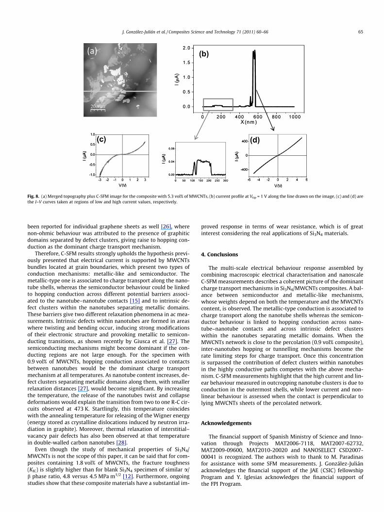
Fig. 8. (a) Merged topography plus C-SFM image for the composite with 5.3 vol% of MWCNTs, (b) current profile at Vtip = 1 V along the line drawn on the image, (c) and (d) arethe I–V curves taken at regions of low and high current values, respectively.
J. González-Julián et al. / Composites Science and Technology 71 (2011) 60–66 65
been reported for individual graphene sheets as well [26], wherenon-ohmic behaviour was attributed to the presence of graphiticdomains separated by defect clusters, giving raise to hopping con-duction as the dominant charge transport mechanism.
Therefore, C-SFM results strongly upholds the hypothesis previ-ously presented that electrical current is supported by MWCNTsbundles located at grain boundaries, which present two types ofconduction mechanisms: metallic-like and semiconductor. Themetallic-type one is associated to charge transport along the nano-tube shells, whereas the semiconductor behaviour could be linkedto hopping conduction across different potential barriers associ-ated to the nanotube–nanotube contacts [15] and to intrinsic de-fect clusters within the nanotubes separating metallic domains.These barriers give two different relaxation phenomena in ac mea-surements. Intrinsic defects within nanotubes are formed in areaswhere twisting and bending occur, inducing strong modificationsof their electronic structure and provoking metallic to semicon-ducting transitions, as shown recently by Giusca et al. [27]. Thesemiconducting mechanisms might become dominant if the con-ducting regions are not large enough. For the specimen with0.9 vol% of MWCNTs, hopping conduction associated to contactsbetween nanotubes would be the dominant charge transportmechanism at all temperatures. As nanotube content increases, de-fect clusters separating metallic domains along them, with smallerrelaxation distances [27], would become significant. By increasingthe temperature, the release of the nanotubes twist and collapsedeformations would explain the transition from two to one R-C cir-cuits observed at 473 K. Startlingly, this temperature coincideswith the annealing temperature for releasing of the Wigner energy(energy stored as crystalline dislocations induced by neutron irra-diation in graphite). Moreover, thermal relaxation of interstitial–vacancy pair defects has also been observed at that temperaturein double-walled carbon nanotubes [28].
Even though the study of mechanical properties of Si3N4/MWCNTs is not the scope of this paper, it can be said that for com-posites containing 1.8 vol% of MWCNTs, the fracture toughness(KIC) is slightly higher than for blank Si3N4 specimen of similar a/b phase ratio, 4.8 versus 4.5 MPa m1/2 [12]. Furthermore, ongoingstudies show that these composite materials have a substantial im-
proved response in terms of wear resistance, which is of greatinterest considering the real applications of Si3N4 materials.
4. Conclusions
The multi-scale electrical behaviour response assembled bycombining macroscopic electrical characterisation and nanoscaleC-SFM measurements describes a coherent picture of the dominantcharge transport mechanisms in Si3N4/MWCNTs composites. A bal-ance between semiconductor and metallic-like mechanisms,whose weights depend on both the temperature and the MWCNTscontent, is observed. The metallic-type conduction is associated tocharge transport along the nanotube shells whereas the semicon-ductor behaviour is linked to hopping conduction across nano-tube–nanotube contacts and across intrinsic defect clusterswithin the nanotubes separating metallic domains. When theMWCNTs network is close to the percolation (0.9 vol% composite),inter-nanotubes hopping or tunnelling mechanisms become therate limiting steps for charge transport. Once this concentrationis surpassed the contribution of defect clusters within nanotubesin the highly conductive paths competes with the above mecha-nism. C-SFM measurements highlight that the high current and lin-ear behaviour measured in outcropping nanotube clusters is due toconduction in the outermost shells, while lower current and non-linear behaviour is assessed when the contact is perpendicular tolying MWCNTs sheets of the percolated network.
Acknowledgements
The financial support of Spanish Ministry of Science and Inno-vation through Projects MAT2006-7118, MAT2007-62732,MAT2009-09600, MAT2010-20020 and NANOSELECT CSD2007-00041 is recognized. The authors wish to thank to M. Paradinasfor assistance with some SFM measurements. J. González-Juliánacknowledges the financial support of the JAE (CSIC) fellowshipProgram and Y. Iglesias acknowledges the financial support ofthe FPI Program.
66 J. González-Julián et al. / Composites Science and Technology 71 (2011) 60–66
References
[1] Riley FL. Silicon nitride and related materials. J Am Ceram Soc2000;83(2):245–65.
[2] Liu CC, Huang JL. Effect of the electrical discharge machining on strength andreliability of TiN/Si3N4 composites. Ceram Int 2003;29(6):679–87.
[3] Guo Z, Blugan G, Graule T, Reece M, Kuebler J. The effect of different sinteringadditives on the electrical and oxidation properties of Si3N4–MoSi2 composites.J Eur Ceram Soc 2007;27(5):2153–61.
[4] Tatami J, Katashima T, Komeya K, Meguro T, Wakihara T. Electricallyconductive CNT-dispersed silicon nitride ceramics. J Am Ceram Soc2005;88(10):2889–93.
[5] Zhan GD, Kuntz JD, Garay JE, Mukherjee AK. Electrical properties ofnanoceramics reinforced with ropes of single-walled carbon nanotubes. ApplPhys Lett 2003;83(6):1228–30.
[6] Balazsi Cs, Fenyi B, Hegman N, Kover Z, Weber F, Vertesy Z, et al. Developmentof CNT/Si3N4 composites with improved mechanical and electrical properties.Composites B 2006;37(6):418–24.
[7] Shi SL, Liang J. Effect of multiwall carbon nanotubes on electrical and dielectricproperties of yttria-stabilized zirconia ceramic. J Am Ceram Soc2006;89(11):3533–5.
[8] Poorteman M, Traianidis M, Bister G, Cambier F. Colloidal processing, hotpressing and characterisation of electroconductive MWCNT–aluminacomposites with compositions near the percolation threshold. J Eur CeramSoc 2009;29(4):669–75.
[9] Ahmad K, Pan W, Shi SL. Electrical conductivity and dielectric properties ofmultiwalled carbon nanotube and alumina composites. Appl Phys Lett2006;89(13):133122.
[10] Rul S, Lefevre-Schlick F, Capria E, Laurent Ch, Peigney A. Percolation of single-walled carbon nanotubes in ceramic matrix nanocomposites. Acta Mater2004;52(4):1061–7.
[11] Flahaut E, Peigney A, Laurent Ch, Marliere Ch, Chastel F, Rousset A. Carbonnanotube–metal-oxide nanocomposites: microstructure, electricalconductivity and mechanical properties. Acta Mater 2000;48(15):3803–12.
[12] Osendi MI, Gautheron F, Miranzo P, Belmonte M. Dense and homogenoussilicon nitride composites containing carbon nanotubes. J NanosciNanotechnol 2009;9(10):6188–94.
[13] Horcas I, Fernandez R, Gomez-Rodriguez JM, Colchero J, Gomez-Herrero J, BaroAM. A software for scanning probe microscopy and a tool for nanotechnology.Rev Sci Instrum 2007;78:013705.
[14] Munuera C, Barrena E, Ocal C. Scanning force microscopy three-dimensionalmodes applied to conductivity measurements through linear-chain organicSAMs. Nanotechnology 2007;18(12):125505.
[15] Li CY, Thostenson ET, Chou TW. Dominant role of tunneling resistance in theelectrical conductivity of carbon nanotube-based composites. Appl Phys Lett2007;91(22):223114.
[16] Nalwa HS. Handbook of low and high dielectric constant materials and theirapplications. Academic Press; 1999.
[17] Pike GE. Semiconductor grain-boundary admittance-theory. Phys Rev B1984;30(2):795–802.
[18] Blatter G, Greuter F. Carrier transport through grain-boundaries insemiconductors. Phys Rev 1986;33(6):3952–66.
[19] Mc Donald JR. In: Barsoukov E, editor. Impedance spectroscopy theory,experiment and applications. Hoboken, New Jersey: Wiley-Interscience, JohnWiley & Sons, Inc.; 2005.
[20] Ahmad K, Pan W. Dramatic effect of multiwalled carbon nanotubes on theelectrical properties of alumina based ceramic nanocomposites. Compos SciTechnol 2009;69(7–8):1016–21.
[21] Ebbesen TW, Lezec HJ, Hiura H, Bennett JW, Ghaemi HF, Thio T. Electricalconductivity of individual carbon nanotubes. Nature 1996;382(6586):54–6.
[22] Kulesza S, Szroeder P, Patyk JK, Szatkowski J, Kozanecki M. High-temperatureelectrical transport properties of buckypapers composed of doped single-walled carbon nanotubes. Carbon 2006;44(11):2178–83.
[23] Zhao YP, Wei BQ, Ajayan PM, Ramanath G, Lu TM, Wang GC, et al. Frequency-dependent electrical transport in carbon nanotubes. Phys Rev B2001;64(20):201402.
[24] Frank S, Poncharal P, Wang ZL, de Heer WA. Carbon nanotube quantumresistors. Science 1998;280(5370):1744–6.
[25] Tsukagoshi K, Watanabe E, Yagi I, Yoneya N, Aoyagi Y. Multiple-layerconduction and scattering property in multi-walled carbon nanotubes. New JPhys 2004;6:3.
[26] Gomez-Navarro C, Weitz RT, Bittner AM, Scolari M, Mews A, Burghard M, et al.Electronic transport properties of individual chemically reduced grapheneoxide sheets. Nano Lett 2007;7(11):3499–503.
[27] Giusca CE, Tison Y, Silva SRP. Evidence for metal-semiconductor transitions intwisted and collapsed double-walled carbon nanotubes by scanning tunnelingmicroscopy. Nano Lett 2008;8(10):3350–6.
[28] Urita K, Suenaga K, Sugai T, Shinohara H, Iijima S. In situ observation ofthermal relaxation of interstitial–vacancy pair defects in a graphite gap. PhysRev Lett 2005;94(15):155502.
Copyright © 2022 FDOKUMEN