
Aalborg Universitet Spacecraft Attitude Determination ... - CORE
Upload
khangminh22Category
view
1download
0
‘\MODEL|NG AND ANALYSIS OF SPACECRAFT POWER SYSTEMS,
bv
Bo Hyung\Cho„
Dissertation submitted to the Faculty of the Virginia
Polytechnic Institute and State University in partial
fulfillment of the requirements for the degree of
DOCTOR OF PHILOSOPHY
in
ELECTRICAL ENGINEERING
APPROVED:
F. C. Lee; Chairman
S. L. Hen icks S. Rahman
VanLandingha V.VorperianOctober,
1985
Blackburg, Virginia

MODELING AND ANALYSIS OF SPACECRAFT POWER SYSTEMS
X Bo Hyung Cho
(ABSTRACT)
A comprehensive large-scale power system modeling is developed to fa-
cilitate the design and analysis of present and future spacecraft power
systems. A two-port coupling method is utilized to provide a modularity
in model building and analysis of the system. The modular approach allows
the model to be flexible, verifiable and computationally efficient. A
methodology for the system level analysis is presented with the ability
to focus on the performance characteristics of an arbitrary component or
subsystem. The system performance parameters are derived explicitly in
terms of the two—port hybrid g-parameter representation of the component
or subsystem, and impedances of its terminating subsystems. From this,
the stability of the system is analytically determined and the subsystem
interaction criteria is observed. Also presented is a model development
from the empirical data employing the complex curve fitting technique.
The technique is especially powerful for large scale system modeling and
analysis where certain components and subsystems are viewed as black boxes
with measurable terminal characteristics. The technique can also be used
to realize a reduced order model of a complex subsystem.
The Direct Energy Transfer (DET) spacecraft power system is modeled Z
to demonstrate the versatility of the comprehensive system model by per-

forming various DC, small-signal and large-signal analyses. Of partic-
ular interest is the analysis of the large—signal behavior of the
nonlinear solar array system by employing the state-plane method. The
analysis of the solar array system operation focused on the transition
mode between the shunt mode and the battery discharging mode is presented.
The subsystem interaction problems in the local component and global
system are illustrated. A methodology for the design and trouble-shooting
of a system dealing with the interaction problems using the g-parameters
is described. Finally, a system level analysis of the DET system using
an empirical data modeling technique is performed.

ACKNOWLEDGEMENTS
iv

TABLE OF CONTENTS
ABSTRACT ii
ACKNOWLEDGEMENTS iv
CHAPTER l INTRODUCTION 1
CHAPTER 2 METHODOLOGY OF MODELING AND ANALYSIS OFSPACECRAFT POWER SYSTEM 6
2.1 Introduction 62.2 Modeling approaches of large scale systems 72.3 Two—port transfer function models 122.4 System analysis approaches using the transfer
function models 162.5 Conclusions 20
CHAPTER 3 SPACECRAFT COMPONENTS MODELING AND ANALYSIS 23
3.1 Introduction 233.2 Switching regulator modeling 253.3 Solar array modeling 583.4 Shunt regulator modeling 683.5 Cable/filter modeling 743.6 Payload modeling 763.7 Conclusions 77
CHAPTER 4 MODELING A DIRECT ENERGY TRANSFER SPACECRAFTPOWER SYSTEM WITH EASY5 78
4.1 Introduction 784.2 Direct energy transfer power system 784.3 EASY5 model generation and analysis 80
CHAPTER 5 ANALYSIS OF SOLAR ARRAY POWER SYSTEM MODES OFOPERATION 85
5.1 Introduction 855.2 Large-signal behavior of solar array operating points 875.3 Analysis of the system operating near the solar
array maximum power point 1035.4 Analysis of the solar array system in the
battery discharge mode 1095.5 Analysis of modes of operation of the direct
energy transfer power system 1295.6 Conclusions 134
v.

CHAPTER 6 SUBSYSTEM INTERACTION ANALYSIS 136
6.1 Introduction 1366.2 Load interaction analysis 1376.3 Source interaction analysis 1466.4 Conclusions 156
CHAPTER 7 EMPIRICAL DATA MODELING AND ANALYSIS 158
7.1 Introduction 1587.2 Model development from frequency response data 1597.3 Review of existing complex curve fitting algorithms 1617.4 Empirical data modeling and analysis of power systems 1657.5 Conclusions
CHAPTER 8 CONCLUSIONS 174
REFERENCES 179
vi

Chapter 1
INTRODUCTION
The ever increasing demand on spacecraft power systems for improved
efficiency and reliability, smaller size and lighter weight, coupled with
lcontinuous growth in dimension and complexity of the spacecraft's” pay-
loads, has focused attention on a major deficiency - the ability to de-
sign, test, and trouble-shoot large scale power systems.
During the past several decades, numerous efforts have been made to
develop new and more powerful techniques for modeling and analysis of
spacecraft power components (equipments) and subsystems. However, when
the components and subsystems are interconnected to form a complex system,A
it is quite difficult to predict the total system response even though
the behavior of individual components may be well understood and docu-
mented. This is due to many undesired interactions that exist among
highly nonlinear components. The need of a comprehensive power system
modeling tool is, therefore, most critical since the elaborate design
verification through integrated systems hardware testing is prohibitively
expensive or often impossible. This is particularly true in the future
space station system since, due to the large dimension and complexity,
the complete system can only be assembled in space. Therefore, a com-
prehensive computer model that can actually predict a system°s local and
global behaviors is most critical for the success of future missions.
Considering the size and complexity of todays spacecraft power
l

2
processing systems, the digital computer is perhaps the only viable tool
for system modeling and simulation. Two general classes of power system
modeling programs appear in the literatures. These are :
•Generalized circuit and system analysis models.
•Dedicated models of specific systems.
The generalized circuit analysis models, as a class, are represented
by programs such as SPICE, SCEPTRE, SYSCAP, ICAP, ASTAP and a number of
others. All have similarities in that they offer a set of typical device
modules which are assembled into a network of interconnecting nodes. This
class of computer programs shares a common drawback, such that with an
increasing number of components, the memory requirements increase dra-
matically. By use of dynamic memory management it may be possible to
analyze a large-scale system, but only at the cost of a geometric increase
in computation time. The labor involved in model—building is rather ex-
tensive and the resulting model, in general, lacks flexibility for future
modifications. Furthermore, the analysis capability of these canned
programs is limited and usually not effective for design aid or
trouble-shooting.
Dedicated models of specific power systems have been used successfully
but only on a limited basis. Typically this class of model is capable
only of DC analysis. Execution speed and cost of such programs tend to
be much less than that for generalized circuit and system routines [1].

3
Therefore, a comprehensive power system model must be capable of per-
forming various analyses - DC, small signal and large signal transient.
The model should have the following attributes :
•flexible for future modification of component models and system con-
figuration,
•accurate to provide sufficient details about the behavior of indi-
vidual components for design and troubleshooting,
° verifiable whenever equipment or subsystem experimental testing is
possible,
•efficient to minimize computer core memory and computation time.
One way to develop a model with such attributes is to modularize var-
ious components of the power system. In Chapter 2, a methodology for
modeling and analysis of a large scale power systmu is presented. A
two-port subsystem coupling method is utilized and its interconnection
law is defined. A system analysis technique is described that defines
the total system as being a doubly terminated two-port network for an
arbitrary subsystem. The system performance parameters are derived ex-
plicitly as functions of the two-port g—parameters of the subsystem (or
component) and impedances of its terminating subsystems.

· 4
In Chapter 3, modeling of various components of the spacecraft power
system is presented. Each component is modeled as an unterminated two-
port. For each nonlinear component, the time-domain simulation model and
the linearized small signal model are developed. The transfer function
models of the g-parameter of individual component and the small signal
lperformance parameters of the terminated component are derived. ”Using
the component models developed in Chapter 3, a sample system model - the
direct energy transfer (DET) spacecraft power system is developed. The °
system model building with the host software system and its analysis ca-
pabilities are described in Chapter 4.
Using the DET system model, various types of system level analyses are
performed in Chapters S through 7. In Chapter 5, various modes of oper-
ation of the DET system are described. The large signal behavior of the
nonlinear solar array power system is analyzed using the state—plane
method. The system behavior near the solar array maximum power point is
discussed.
The operation of a battery discharger circuit and the design consid-
erations suitable for a wide range of operations (i.e., from the no-load
to full load) of a feedback compensator are described. The complete
system mode of operation including the transition mode between the shunt
mode and the battery discharging mode is illustrated.
In Chapter 6, subsystem interaction problems are illustrated. The
local and global interactions are described and a methodology for the
design and trouble-shooting of a system dealing with the interactionI
problems is presented. One of the most attractive approaches for modeling
.4

5
and analysis of complex large scale systems is the empirical data modeling
technique. In chapter 7, empirical data modeling employing a complex
curve fitting technique is presented. The system level analysis using
this technique is performed by defining an arbitrary subsystem as a black
box for which the curve fitted analytical model is realized from the em-
pirical data. The complex curve fitting technique is extended to derive
a reduced order model for a high order subsystem. Conclusions are pre-
sented in Chapter 8.

Chapter 2
METHODOLOGY OF MODELING AND ANALYSIS OF
SPACECRAFT POWER SYSTEMS
2.1 Introduction
This chapter discusses a modeling and analysis methodology of large
scale systems. Section 2.2 uses the modular concept that a large scale
system may be defined as an interconnection of many individual subsystems.
This idea is particularly attractive for spacecraft power systems con-
sisting of many individual components since each component may be supplied
by a different vendor where performance parameters and design information
are documented as a stand alone equipment (component). By defining
standardized interconnection laws between each component, a system can
be analyzed and synthesized using the information of the individual com-
ponent modules. In Section 2.3 the terminal characteristics of a singly
and doubly terminated two-port subsystem are derived as transfer function
models for a system linear analysis. In Section 2.4, based on the model
representation derived in Section 2.3, system stability is analyzed. This
section further addresses the compatibility and incomparability of indi-
vidual components in terms of their terminal characteristics and the
interconnection schemes. Performance degradations and system instability
as a result of undesired component interactions are illustrated. Con-
clusions are presented in Section 2.5.
6

7
2.2 Modeling approach of large scale systems
As discussed in Chapter l, defining a complete spacecraft power system
entirely in terms of circuit elements is not feasible. A practical ap-
proach is to consider that a large scale system can be defined by the
interconnection of many smaller subsystems. The system dynamics, there-
fore, stem from the individual subsystems and their interconnection laws
that identify the signal flows among them. Due to the complexity of the
individual components and their interconnection scheme it is usually very
difficult to predict the system°s overall behavior. A desirable analysis
or synthesis procedure for a large scale system is the separation of these
two levels (component and system). One thus prefers an analysis or syn-
thesis procedure to be based, on one hand, on“lggal"
subsystems and, on
the other hand, on the "global" interconnection laws.
In order to utilize the modular concept, each component should be
modeled as an unterminated two-port network because the terminal charac-
teristics of both source and load are unknown until the complete system
is configured. The interconnection law should not only describe accu-
rately the signal flows between the subsystems but also be standardized.
There exist several kinds of two-port representations such as impedance,
admittance, chain, and hybrid matrices. The impedance or admittance ma-
trices cannot be used as a standard interconnection law because their
inputs and outputs are in alternate forms. The chain matrix is not as
flexible as the hybrid matrix because it only characterizes a system in
uni—direction. For example, the chain matrix can describe port·l of a
two-port subsystem as a function of its load (which may be connected in

8
cascade in n two-port subsystems) that is connected at port-2 as shown
in Eq.(2.l).
e 1 e nl _ 2
1fl:I1lM)):hHlf1 fz" (2.1)
where the subscripts and superscripts represent the port numbers and the
.1:11 .J component, respectively.
However, quite often, it is necessary to analyze a two-port subsystem
as functions of both its source and load. Thus, the information flow can
be obtained in both directions. Fig.2.1 illustrates the interconnection
law for unterminated modules. Each component, in general, receives two
inputs vl and iz from the preceding and following modules, and provides
two outputs il and V2 to the adjacent modules. The terminal character-
istics of each component are described by the matrix equation called
"hybrid g-parameters" in Eq.(2.2).
il $11 $12 V1
V2 $21 $22 iz (L2)
For modeling a two-port, one can always define the output and input var-
iables as shown in Fig.2.l. For example, a single stage LC low-pass
filter can be modeled with state equations as shown in Fig.2.2. Since
these unterminated two-port components have the same interconnection law,

9
.· ·
b ' blf *5 *1 *2(-———
<-—-—- < <*T
•+ +
• •+ +
•
CÜMPUNENT b COMPUNENT bV1a Vza V1 V2l-p
-1-) —·-l->i-P
ra 1' b'
Figure 2.7 Two—port subsystem coup/ing using the hybrid G—m0trix‘

4 10
47.L-+
——> +'1
RcV V1
+ 2
C vc
iz -(R9.+Rc) -i iz L 2 vl
= L L + L L1 1 .VCF 0 VC 0 F
12
il -1 0 iz 0 0 vl= +
V2 RC 0 VC 0 RC iz
Figure 2.2 Example of an unterminated two—port mode/ingwith state equatlons

ll
they can be interconnected arbitrarily to form a system.
Having identified the two~port component coupling approach, efforts
have been made to find a software system which can be adapted to multi-
port component modeling and system integration. The program EASYS de-
veloped by Boeing Computer Service has been selected as the host software
system.
The EASYS software [2] provides a modular approach to dynamic system
model building and analysis. It was chosen particularly for its effective
means of assembling complex component modules into a system. Predefined
component modules can be stored in the EASYS component library. The
component modules can have several input and output ports and, in each
port, information can flow into and out of the port. All detailed con-
nections of signal paths between component blocks are programmed with
minimal user intervention. More details about the EASYS program will be
described in Section 4.2.
For a large scale spacecraft power system, the large signal performance
evaluation is invariably limited to tactics closely identified with
time-domain simulation techniques. The actual operating point trajecto—
ries or transient responses due to the large signal disturbances can be
simulated by a digital computer. In this way, the existence of unstable
solutions can be observed along with peak values and actual waveforms.
Thus, the model development of each nonlinear component of a spacecraft
power systems involves two separate models, the large signal time-domain
simulation model and the small signal linearized model.

12
For time—domain simulation, the EASY5 numerical integration routine
calculates current values of the states and output variables for each
component from the input values. It then passes along the output values
according to the interconnection law. There are seven different types
of numerical integration routines available in EASY5. Each offers dif-
ferent numerical stability and computational efficiency dependent on the
type of nonlinearity of a system. To examine the approximate large signal
behavior of a system analytically, rather than by time-domain simulation,
one may simplify the system focusing on a particular component of inter-
est. For instance, the large signal behavior of the solar array system°s
operating point can be analyzed by simplifying the system to a second
order nonlinear system as illustrated in Chapter S.
For the small signal linear analysis, various types of classical linear
system theories can be adapted. The methodology of large scale system
analysis is described in the following sections.
2.3 Two·port transfer function models
To analyze the two-port component or subsystem in Fig.2.l, one needs
to identify the G-matrix in Eq.(2.2). From Eq.(2.2), the g-parameters
can be described in the form of transfer functions. As Fig.2.3 illus-
trates, each parameter can be identified by using an appropriate
sinusoidal current or Voltage excitation. lt is important to notice that
the g—parameters are identified in terms of measurable (observable)
quantities, thus the model can be verified. This modeling technique is
particularly useful when the component is best treated as a black box due

l3
'1C
+
Ö "=I
'1<l·—
+
V2 9 ‘¤
ilgu = i :0 ; open circuit input admittance
1 2
V2gzl = T- i :0 ; open circuit voltage trnasfer function
1 2
ilglz = V :0 ; short circuit current transfer function
2 1
V2g = —+
: ; short circuit output impedance22 12 vl 0 a
Figure 2.3 Two·port g-parameter rea/izations

14
to its complexity or unknown nature. The empirical data of the two-port
g-parameters can easily be obtained, from which an analytical closed-form
model is realized employing the complex curve fitting technique. The
empirical data modeling approach will be discussed in Chapter 7.
The two-port modeling approach allows one to analyze the complete
system with a focus on the local behavior of a particular component or
subsystem. As far as the two-port subsystem is concerned, the entire
system can be considered as a doubly terminated two-port system as il-
lustrated in Fig.2.4. The quantities ZS and ZL are the source and load
impedances seen by the two-port subsystem. Notice that the equivalent
circuit may be obtained by replacing the generator and ZS by its Norton
equivalent in the circuit. As shown in Fig.2.4 four important parameters
can be realized in terms of the two port g-parameters ZS and ZL.
g21‘ZLGV =
A + zZL - ZS. G gll.ZS. L (2.3)
g1l°g22 + g12‘g21 ' ZL
gzl (2-4)
gll + AG / ZLYi:-———
1 + g22 / ZL (2.5)
g22 ' AG Zs
1 - gll. S (2.6)

‘ 15
I1 iz
ä‘“— " +
G ID G = V2L
Y. ZI O
V2GV = ; forward Voltage transfer function
1
ilGi = ; reverse current transfer function
2
ilYi = ; load terminated input admittance
l
V2Zo = -T- ; source terminated output impedance
2
Figure 2.4 Transfer functions of the doubly terminated two·port

16
where
AG = gllg22 ' g12g2l
These parameters play important roles in the analysis of the system dy-
namics especially the interactions among the various subsystems.
2.4 System analysis approach using the transfer function models
One of the major concerns in analyzing the large scale spacecraft power
system deals with undesired interactions among components and subsystems.
As a system becomes more complex, many undesired interactions occur and
they create a large degree of uncertainty in the system response and
stability even though each component may be well-behaved and understood.
Using the presently existing modeling techniques it may be possible to
simulate the entire system by a digital computer. However, the results
obtained from the computer simulation often do not provide physical in-
sight and thus give very little design information for future design
changes and trouble-shootings. Based on the modeling approach described
in Section 2.3 the system can be analyzed with an emphasis on either the
local behavior or the global behavior. The analysis allows one to
trouble-shoot the interaction problem at any system level.
From Eqs.(2.3) and (2.4) the stability of the total system can be di-
rectly analyzed by investigating the poles of the transfer function GV
and Gi. However, since GV and Gi may be of complex form, interactions
among ZS, ZL, and the two-port subsystem may not be easily obtainable.

17
Instead, one can investigate the source and load interaction problems
using the quantities Yi and Z0 in Eqs.(2.S) and (2.6), as illustrated in
Fig.2.S.
The line transfer functions in Fig.2.5 can be written as follows.
From Fig.2.5a,
V2 ZL 1 1}{L:——-—::—-§—-.
*1vs Zo + ZL 1 + ZO/ZL l + TL (2.7)
and from Fig.2.5b,
vl 1/Yi 1 1HS:-l—:—i•:-—-ii-t;.—.
VS l/Yi + ZS 1 + ZS.Yi l + TS (2.8)
Eqs.(2.7) and (2.8) shows that the system characteristic equation is 1 +
TS = 0 or 1 + TL = 0, respectively. Hence, the system is stable if the
quantity TS in Eq.(2.7) or TL in Eq.(2.8) satisfies the Nyquist criterion
that is, the system is stable if the number of counterclockwise
encirclements of the point (-1,0) in s—plane of the polar plot of T's is
equal to the number of the right-half plane (RHP) poles in T. This
statement still may be too general unless the number of RHP poles in TS
or TL are identified. If we assume that the elements in Eqs.(2.7) and
(2.8) are all stable quantities, i.e. no RHP poles, then the Nyquist

18
II
SUB- iI6 SYSTEM 4- ze I zi +I
II
Zs
8.
III
I SUB-6 + ze I vi + SYSTEM
II
' zh. L
Figure 2.5 Subsystem interoction porometers
(0) lo0d inter0ction (ZO vs ZL)
(b) source interoction (Z5 vs Zi)

19
criterion can be restated as; the system is stable if the polar plot of
TS or TL does not encircle the point (-1, 0).
To analyze the interaction problems of a two-port with ZS and ZL, it
is necessary to check the above assumption that the quantities ZS, ZL,
Yi and Zo are all stable (i.e., no RHP poles). If any of these are un-
stable then an interaction has already occurred with an unstable quantity
and the analysis should trace back until the point of the undesired
interaction is found. To do this consider Fig.2.6 which elaborates the
system in Fig.2.&. The quantities in Eqs.(2.3) through (2.6) of thejth
component can be expressed in terms of the preceding (j-lth) and the
following(j+lth)
components.
J: J'lZs Zo
(2.9)
j=
j+1 (2.10)ZL 1 / Yi l
From Eqs.(2.5) and (2.6),
J_ JJ J, J·1j gzz AG .ZS gzz AG.ZO
Z°=1- jzj = 1- jzj“1 (211)gll°S g1l'o ‘
.1 .1.1 .1 J+lj gll + AG /ZL gll + AG.Yi
Y.=1 1 1 1 1+11 + gzz .ZL 1 + g22 .Yi (2.12)
From Eqs.(2.9) through (2.12) the stabilities of ZS, ZL, Yi and ZO for

l20
j·1 Kj·l jZ0 ZL Zo ZL
O O • • • •. th
OMP COMP QQMP
5 Y 5 3+1 3+1ZS i ZS Yi
Figure 2.6 Rea/izotion of impedances for cusccde components

2l
any two-port can easily be checked and the possible undesired interaction
points detected. For instance, the stability of output impedance of the
jthcomponent
Zoj can be determined from Eq.(2.l1) by applying the Nyquist
criterion to the product of -g1lj and Zoj·l. Since each unterminated
component (g-parameters) is assumed to be stable and ifZoj is unstable
while Zoj-1 is stable, then the undesired interaction occurs between thejth
component and its source impedance Zsj. The same argument holds for
the load interactions such that if Yij is unstable while Yij+1 is stable
then the undesired interaction occurs between thejth
component and its
load impedanceZLj.
In other words, the stability of the doubly termi-
nated two-port component can be established as follows. First, using
Eqs.(2.9) through (2.12) the stability of ZS and ZL must be examined then
using Eqs.(2.ll) and (2.12) the stability of Yi and ZO (singly terminated
two-port) can be determined. If Yi and ZO are stable, which implies ZS
and ZL are also stable, then the stability of the doubly terminated two-
port system can be established by applying the Nyquist criterion to TS
and TL in Eqs.(2.7) and (2.8).
2.5 Conclusions
In this chapter the proposed modeling and analysis techniques of large
scale systems were discussed. A two-port subsystem coupling method is
utilized such that a system is broken into manageable pieces. Each com-
ponent is modeled as an unterminated two-port and the system is configured
according to the interconnection law.

22
The stability of a linearized large scale system can be analyzed with
a focus on either local or global behavior. The analysis not only de-
termines the stability of the total system but also identifies the unde-
sired interactions which occur at various component levels. Thus, the
design criteria for components and their integration can be established.
The modular approach allows one to pinpoint the undesired interaction
point to assist in trouble-shooting. The modular approach also allows
the analysis to be performed with well-defined physical quantities (i.e.,
impedances) which are also observable and measurable both analytically
and empirically. The analysis technique is based on well-known classical
linear circuit theory, two-port network theory and Nyquist theory so that
any practicing engineer can utilize the technique for design, analysis
and trouble—shooting a large-scale system. Various types of the system
level analyses for the Direct Energy Transfer spacecraft system are per-
formed in Chapters S through 7.

Chapter 3
SPACECRAFT COMPONENTS MODHJNG AND ANALYSE
3.1 Introduction
Components of spacecraft power systems are inherently nonlinear. As
a result, their behaviors due to large signal and small signal disturb-
ances can be quite different. For the analysis of the small signal dy-
namics, such as stability, input/output impedances, and
audiosusceptibility, the model can be developed by linearizing the non-
linear components about an operating point under the small signal as-
sumptions. These small signal models are very useful since all of the
well established linear system theories can be applied. Also their ana-
lytical closed forms provide useful information for designing the system.
However, the small-signal models can not predict the large-signal behav-
ior such as stability in large, initial Start·up and step transients, and
other nonlinear modes of operation (i.e., protection, saturation, etc.).
Therefore, it is necessary to generate a small signal model and large
signal model for these nonlinear components to analyze the following
performance categories: dg, small signal ac, and large signal transient
responses.
It is desirable that various components in the spacecraft power system
be modeled with maximum flexibility, using any one of the following rep-
resentations: state eguations, transfer functions, empirical data, and
combinations of those. One may choose one of these modeling techniques
23

24
best suited for a particular component. For instance, quite often a
component can be virtually a black box due to either complexity or unknown
nature, then empirical data modeling is the only resort. For a component
of piecewise linear nature, such as switching converters, the state space
modeling is most convenient. For a linear component, the transfer func-
tion. model often suits best because it provides more design insight.
Integrating these component models in different forms can be done with
minimum user's intervention employing the host software system EASY5.
Details for the system modeling are discussed in Chapter 4.
As described in Chapter 2, characteristics of the g-parameters for each
component should be analyzed as an unterminated two-port network. The
system level analysis can then be carried out based on the g—parameters
of individual components. In this chapter, modeling and analysis of the
following spacecraft components are discussed.
•Switching regulator - Section 3.2
•Solar array · Section 3.3
•Shunt regulator - Section 3.4
•Filter / cable - Section 3.5
•Payload · Section 3.6

25
3.2. Switching regulator modeling
Because of high efficiency, small size and light weight, switching
regulators are widely used in spacecraft power systems. Switching regu-
lators can be characterized, as shown in Fig.3.1, by the three basic
functional blocks: power stage, analog feedback controller, and digital
signal processor.
The power stage consists of energy storage elements and switches.
Transfer of the input power to the load is controlled by the duty ratio
of the switch (transistor). The analog feedback controller usually con-
tains an error amplifier and a compensation network. For a single loop
control it senses the output (load Voltage), and for a multiple loop
control it senses the output and states (i.e., load Voltage, inductor
current, capacitor Voltage). The digital signal processor includes a ramp
generator, a comparator, and latches. It takes the control Voltage from
the analog feedback and converts to the pulse width modulated (PWM) signal
which controls the switches in the power stage switch.
Switching regulators are inherently nonlinear and discrete. The power
stage has several different topological modes controlled by the
switch(es) whose switching time is PWM controlled by the feedback con-
troller. The state equations, in general, cannot be solved unless the
system is linearized about an operating point. The linearized model can
be used to analyze the small signal behavior about an operating point
using the relatively simple linear system analysis techniques such as Bode
plots, root locus, etc.

26
_ powen suseVi Eu., « Vo
- I
L li°§||§ E
., L ,%
COMPENSATOR
- dlgltal SÜQHBI iDYOCESSOT {tnresnoldsetecwr
-- TER Ell /L/l : =
Figure 3.7 Switching regu/ator model

27
Since there exist many different types of power stage topologies and
control methods, the large signal behaviors of a regulator depend largely
on the type of power circuit topology and control. Thus, for maximum
flexibility, it is best to develop models for each functional block as
independent modules. A regulator can then be configured by collecting
appropriate pre-defined modules for each functional block. Also any of
these block modules can be freely replaced with alternatives, it provides
maximum flexibility in building a variety of regulators. Development of
each functional block are as follows.
3.2.1 Power stage modeling ·
Generally, three different circuit topologies exist in the course of
a complete switching cycle. A converter is characterized by three sets
of state equations during a switching cycle as follows
x = Alx + Blu
A y = Clx + Elu , for interval dnlTS (3.1)
x = Azx + Bzu ,
y = Czx + Ezu , for interval dn2Ts (3.2)
x = A3x + B3u ,
y = C3x + E3u , for interval dn3Ts (3.3)

28
Here x is the state vector, u the input vector and TS the switching pe-
riod. Ai and Bi (i=l,2,3) are square matrices which describe the three
circuit topologies and the effects of the input vector u. The switch duty
ratio is represented by the fractional quantity dnl, and dnl + duz + dn3
= l. These three matrix equation can be combined into one by using the
three switching functions shown in Fig.3.2. With use of these switching
functions, a single state equation suffices to describe the converter as
in Eq.(3.4).
. 3x = Z [A.x + B.u]d.(t) ,
i=l 1 1 1
3y = Z [Cix + Eiu]di(t) , i = 1,2,3 (3.4)
i=l
where di's are either 0 or l depending on the specific time interval in·
volved.
Eq.(3.4) is not only discrete but also nonlinear because di(t) is a
function of the state vector x and the input vector u. The power stage
model showing in Eq.(3.4) is directly implemented with the appropriate
switching function for the time-domain model. The intervals defined above
include the possible inductor current discontinuous conduction mode
(DCM). For the continuous conduction mode (CCM), there are only two
switching intervals, dnlTS and d¤2TS. In the time-domain model, these
two different modes of operation (DCM or CCM) are naturally determined
depending on circuit parameter values and input and output requirements.

29
I4-i TS l-)I
1
0I I
Y III
II I
HI I
II I I I I I I I
I I II I I
d2(t) I I I| I II I0 II
I I I I 7333I I I
I I I I I I I II I
d3It) I II II I
j}I·—
D2 TS -1I-I
Figure 3.2 Switching functions

30
However, the small signal models for CCM and DCM are quite different be-
cause of the additional constraints of the state,
di = 0dt (3.5)
and .
i = f(¤„Y,d¤l,L,TS) (3-6)
Therefore, it is necessary to include a step to determine whether the
converter is operated in CCM or DCM for the small—signal model by checking
the boundary condition between these two modes. From Eq.(3.4), the small
signal power stage model can be generated as follows.
Linear small signal modeling of switching converter power stage
For the small signal model, there exist various types of techniques
such as state space averaging [3], discrete—averaging [4] and discrete
technique [5]. Among these, the state space averaging technique is chosen
for this study because it is simple and provides physical insight into
the system, thus it is better suited especially for large system analysis.
The small signal modeling in this section will be carried out for the case
of the constant frequency controlled regulator operating in the CCM. The
fundamentals of the state-space averaging are reviewed as follows.
Averaging: First the switching functions di(t) are averaged as shown
in Fig.3.3. For the CCM where d¤3 = 0, let the averaged values of the

31
switching functions be
dl(t) = d
—
=
•—
='d2(t) 1 dl(t) d (3.7)
Both dynamic and static equations for the two (in CCM) switched intervals
in Eq.(3.4) are averaged by summing the equations for each intervaldniTS
multiplied by the averaged switching function di(t). It results in the
following continuous system which represents the average effect of the
circuit across the whole period TS.
•_
I, Ix — (Ald + Azd )x + (Bld + Bzd )u
y = (Cld + C7d°)x + (Eld + E2d')u (3.8)
where x and y represent the average state and output.
Perturbation : Suppose that the duty ratio changes from cycle to cy-
cle, that is, d = D + d where D is the steady state (dc) duty ratio and
d is a superimposed (ac) Variation, as shown in Fig.3.3. The notation
used throughout this section is that dc or steady state values are re-
presented by upper case letters, and perturbations by lower—case with
carets. The corresponding perturbations of other quantities can also be
expressed as

32
d(t)1
I ' d· I ·.1
IK I”
'. __jD
.¤Ü·—-—I "’
Ad(t)
I I Zi
0Figure 3.3 Averaging the switching functions
—··—· : steady state
— : perturbed small signal

33
d' = l - d = (1 — D) - d = D° - d
x = X + Ä, u = U + G, y = Y + y, (3,9)
Substituting these into the averaged equation (3.8), it becomes
é = AX + BU + A; + B8 + [(A1·A2)X + (Bl·B2)U]d
A AA
+ [(A1·A2)x + (Bl·B2)u]d
§ = CX + EU + C; + EG + [(Cl·C2)X + (El—E2)U]d
A /*"+ [(Cl·C2)x + (E1·E2)u]d (3.10)
whereZ
I=
IA DAI + D A2 , B DBl + D B2
_ I=
IC — DCl + D C2 , E DE1 + D E2 (3.11)
The perturbed state-space description is nonlinear owing to the presence
of the product of the two time dependent quantities x and d.
Linearization: Let us now make the small signal assumption such that
A ^ A Au d x y
·—— << 1, -—· << 1, ·—- << 1, and *—· << 1 (3.12)U D X Y

34
Using these small signal approximations, the nonlinear second order terms
in Eq.(3.l0) can be neglected, and the following linear time invariant
system is obtained:
SS = ASS + BG + P8
= C; + EG + Qd (3.13)
where
P = (A1 — A2)X + (Bl - B2)U
Q = (C1 - C2)X + (El - E2)U (3.14)
By collecting the dc terms from Eq.(3.l0), the steady state solutions are
x = -A-1BU
Y = (-CA-IB + 1a)u (3*13)
The small signal solutions can be obtained by taking the Laplace transform
of Eq.(3.l3).
§ = Huxlu + Hdxä (3.16)
§ = Huylu + Hdy3 (3.17)

35
where
Q-1
··:· A = Hux = (SI ·A) B (3.18)u d=0
2 -1T A = Hdx = (SI ·A) P (3.19)d u=O .
»Y
-5- 8:0 = Huy = C Hux + E (3.20)A
Y——- = H = C H + Q (3.21)Ä G=0 dy dx
EqS.(3.16 - 3.17) describe the power stage of Switching converters with
unterminated input and output. The differences between the above model
and the conventional models for the load terminated case are illustrated
in the following example.
Example: Let us consider a boost converter, as shown in Fig.3.4. For
Simplicity, let us assume the Switch is ideal and RC = O, Rz = 0. The
two Switched models are as shown in Fig.3.5. For choice of State vector
xT= [il V2], the state equations become:
i) interval dlTs ii) interval d2TS
1 1 1‘z° ° r ‘r
°A1 = 0, Bl =0 Ä-
A2 = -_L 0, B2 =
0 _lC C C

36
'1 L 11, 12
+ R1d
X +
+Rc 1
V1 V2vc c
FlgUl'8 3 .4 Boost COl7V€f‘t€f'pOW€f‘
stage
i) intervul dT$ ii) interval d'T$
11 iz 11 12<r <i er <—-
‘+ + + *-12 ++V1 V1 V1 " V1vc vc
Figure 3.5 Two switched circuit models of the circuit in Fig.3.4

37
Cl = C2 = I, El = E2 = O (3.22)
(Note that, for simplicity, the sign convention of the states and outputs
are purposely chosen so that the states are identical to outputs.)
From Eq.(3.l1) the averaged power stage coefficient matrices are
D' 10 L L 0A = , B = C = ID
’1
’**6* O O (3.23)
Using Eq.(3.15), the steady state solution is
I1 1 I2Y:X: =
——DI
V2 V1 (6.24)
The control coefficient matrices using Eq.(3.l4) become
-.‘liP = D L Q = 0
I2 (3.25)D'c ,
The small signal model for the power stage is obtained from Eqs.(3.l8)
through (3.21) and using (3.23) through (3.25) results in

38
C 1
^DIZ DI
Y 1 (3 26)H :-—-:-— °
UYii A
1 L__ ___ sDI DIZ
I C V
§ 1 D D I2H =
___=
___ (3.27)dy
E A V1 L I2——— (1 + ———— s)
IZ ID D V1
where
A = 1 + sz/wol, wo = D' 1 JEE (3.28)
It is noticed that the open loop transfer functions in Eq.(3.26) and
(3.27) have infinite Q (with ideal elements), which clearly implies the
unterminated system. However, the control to output transfer function
in Eq.(3.27) carries the dc input information, V1 and I2. This is due
to earlier assumption that the model describes the behavior of the regu-
lator about a known steady state operating condition. From the state-
space averaged model, the A-matrix does not carry steady state information
while the control matrix P does. This may be seen more clearly in the
linear equivalent canonical circuit model in Fig.3.6 which can be gener-
ated either from the state-space equations or from the circuit averaging
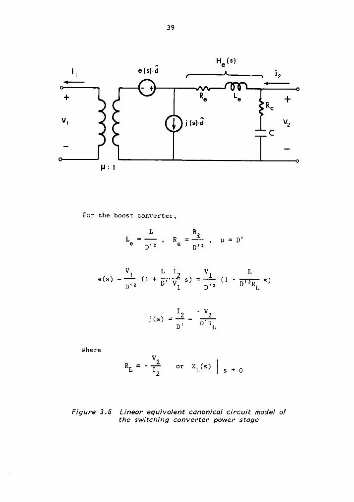
39
A Heß)i1 e(s)-d , E2
••(
+ Re Le+
Rc
V1 i($)·ä V2C
H: 1 .
For the boost converter,
L R;L = l : —- : 'E D'2
Ü Q D
V L I V L1 2 1@(5) (1 + —r‘—· s) =i (1 — ——— s)D., D vl D., ¤'*RL
1 — V. 2 21<S> =—=D'L
where
R — V21:%; °*Z1<S>lS»11
Figure 3.6 Linear equiva/ent canonicai circuit model ofthe switching converter power stage

. 40
technique [3]. In the circuit model the control dependent sources e(s)
and j(s) are functions of the steady state input values while the effec-
tive filter transfer function, He(s), is still unterminated. Hence, if
a regulator is terminated with a resistive load RL, the same RL would
appear in e(s), j(s) and He(s). However, if a regulator is terminated
with a frequency dependent load ZL, only the steady state dc value of ZL
(i.e., RL or V2/I2) appears in e(s) and j(s) while He(s) is terminated
with ZL.
This can be shown from the load terminated open loop transfer func-
tions. For instance, the input Voltage to output Voltage transfer func-
tion becomes
r V2 1 1 1[
HVL$1 a=0, zL D' L S2 D' 6 (3.29)
(1+is+—)•1 1D ZL wo
and the control to output Voltage transfer function is
1 --—L—- s
/~ D°2RV2 V1 LH =-1-
=——•-l——l—————Ee(s)H(s)dL d ü=0, zL D'* L sz
° (3.30)( 1 +
————- s +-———)¤1 1D ZL wo
where RL = - V2 / I2

41
The analysis of the complete regulator using the above results is pre-
sented in Section 3.4.
3.2.2 Analog feedback controller
The commonly used analog feedback controller is basically linear for
normal modes of operations. The controller can be modeled by either
transfer functions or state equations.
The transfer function model, in Eq.(3.31) provides more design insight
so that both analysis and synthesis of the controller can be done quite
easily. Pole-zero compensations of the closed loop system can be directly
implemented using the Bode plot technique.
wm ( 1 + s/wzl)( 1 + s/w22)
F(s)s( 1 + s/wpl) (3.31)
However, the second order effects of the feedback, such as the steady
state switching ripple component, is lost.
Modeling with state equations can describe the circuit in more detail,
and can easily include the nonlinearities such as op—amp saturation, soft
starter and protection circuits. However, the circuit topology must be
pre-fixed and generally, the model requires more memory space. Also, the
model does not provide direct information about the location of poles and
zeros to facilitate design of feedback compensator.

42
Iß V2
,...-......MJ] - ,I F II I II II II II II II II II "VreI= II Ä I
vc & 1 •• un an 1 un 1 —• 1 1 1 1 •- _•|
F” ””'''””''''"I
II II II II II II II ,7,Vmf II II
Fvl v I
I................I I
vc=Fii£+Fv v2
Figure 3.7 A feedback compensator (two-/oop)

43
The choice of model depends on its objective. For design and frequency
domain analysis the transfer function model suits better; and for more
accurate time-domain analysis and simulation the state equation model may
be the better choice. The model developed for this study includes both
modeling techniques. .
Fig.3.7 illustrates a typical multiple loop controller for switching
regulators. The controller senses the state (inductor current) and output
(output voltage). The sum of the state and output compensators (Fx and
FY) is the control voltage, vc, as described in Eq.(3.32).
vc = - (Fx x + Fy y) (3.32)
The compensators for a regulator employing the inductor (or switch) cur-
rent and output voltage sensed feedback become
Fx = [ Fi 0 ], Fy = [ 0 FV ] (3.33)
3.2.3 Digital Signal Processor
The digital signal processor (DSP) converts the output control signal
vc from the analog feedback controller into discrete-time pulses to con-
trol the ON-OFF of the power switch. The DSP includes the threshold de-
tector (comparator), the ramp function and the latch circuit.

44
The threshold detector compares the input control signal, vc, and the
reference signal (either dc or the ramp) to generate the trigger signal
for the transistor OFF command. The latch circuit then generates the PWM
signal, d(t), as shown in Fig.3.2 to the power transistor. For the mul-
tiple loop control, the input control signal, vc, is the sum of the out-
puts of each feedback loop. In this case vc may include the ramp function
(from the inductor current or switch current feedback), then the external
ramp function can be optional, which quite often is needed to stabilize
the system operating more than 50% duty ratio. Fig.3.8 illustrates this
multiple loop case. For each different duty ratio control law such as
constant frequency, constant‘TOn and constant Toff, the DSP model should
be different. These different modules are stored in the component module
library, as in the case of power stage models.
For the small signal model, the transfer function from the control
signal vc to the duty cycle modulation d is obtained as in Eq.(3.34) using
the describing function technique.
d = FM·vC (3.34)
3.2.4 Switching regulator small signal modeling and analysis
Connecting the power stage, analog feedback controller and the digital
controller (Figs. 3.6, 3.7 and 3.8) together completes the small signal
regulator model as shown in Fig.3.9. This unterminated regulator is ready

45
PROTECTIQN
VG„“”„I¤ {
GDNIPARATGR
”D”
LIMITFigure3.8 Pulse—width—modu/ator (PWM)

A6
to be connected into a system. Analysis of the doubly terminated regu-
lator can be carried out using the g-parameters of the regulator, The
g-parameters can be derived either from the circuit model shown in Fig.3.9
or from the block diagram representation in Fig.3.lO. The block diagram
model in Fig.3.l0 which uses transfer functions can describe any type of
converter topology and associated controls. While the model shown in
Fig.3.9 is circuit oriented, and it does provide physical insight into
the system.
The closed loop transfer functions from the the input vector Ü to the
output vector y, the G—matrix of the regulator, can be directly derived
from the transfer function model in Fig.3.l0.
3i==[I + T]—l
H - FM·H ·F ·[ [I + T ]-l H ] (3.35)G
eq uy dy x x ux
where
- -1 _Teq—FM Hdy [py px[[1+Tx] pdx-py pM]] (3.36)
TX = Hdg Fx·FM (3.37)
Using the g-parameters in Eq.(3.35), performance parameters of the regu-
lator operating in the system such as stability, audiosusceptibility,
input and output impedances etc. can be derived as functions of impedances
of its terminating subsystems.

47
i ^ i iz1 e(s)-d J-_ (__
° +•
¤ +
v1 vz
lA
° KVH •¤FY
Figure 3.9 Small signal model of switching regulators

48
u2 >< 1 Qy2 x1' + Ü °
2 x 2 +Hu!
2 x 2 2 x 1
++ A8 E d
2 x 1,„ HX dx
E w 11 x 2 1 x 2
Figure 3.70 Small signal transfer function model ofswitching regulator

49
Analysis of a complete regulator is illustrated in the following example
using the boost converter power stage derived in Section 3.2.1. For
simplicity, a single loop (output voltage feedback) control is used.
Example: Analysis of the boost regulator using the g-parameters
For single loop output feedback control, the compensators are
Fx = O, Fy = [ 0 FV ] (3.38)
and let the PWM gain be FM.
The closed loop input to output transfer functions in Eq.(3.35) becomes
-1G = I + FM H F H 3.39[ dv Y] uv ( )
Using the results of the power stage equations in Section 3.2.1
(Eqs.(3.26) and (3.27)), the g-parameters in Eq.(3.39) are
1 FM I2 V1g =--——-—(l+T)Cs+—--—(1-C——·s)Fll A (1+1*G) 1)'= G A ¤' 12 V (3.40)
1 1 FM I2 V1g = —-(1+T)—-—·;Ls(l-C—s)F12 A (1+1*G) D' G D' A ¤'° 12 V (3.41)

50
g = i..1 .L21 A (1+TG) D, (3.42)
g = 1 L S21 A (1+TG) D.; (3.43)
whereV
A = 1 + s=/AOZ (3.Aa)
FM V1 L I2T = ————-—- (1 + ————— s) FG A D" D°V1 V (6.6.6)
Here, 1 / A is the effective filter transfer function He(s). TG is the
loop gain defined at Point X for the unterminated regulator shown in
Fig.3.9. The stability of the unterminated regulator can be determined
using the quantity TG. The Bode plot technique can be used to check the
Nyquist stability criterion. Using Eqs.(3.40) through (3.45), the total
system can be treated as a doubly terminated two-port system focusing on
the switching regulator. The system analysis can then be carried out by
defining the source and load impedances seen by the regulator.
As described in Section 2.4, a doubly terminated regulator (two—port)
can be analyzed in two-steps. First, by considering the load terminated
regulator (one-port) with ideal source and then including the source
impedance ZS. These steps when compared to the expression for a doubly
terminated two-port system in Eqs.(2.3) and (2.4), provide more physical
insight into the system analysis especially for the interactions from

51
either the source or the load to the regulator.
Singly (load) terminated regulator:
Suppose that the regulator is terminated by a load impedance of ZL,
which is frequency dependent with a dc value of RL, as shown in Fig.3.ll.
The line transfer function from V1 to V2 is
V2 $21 $21GVL 6 1 + g /2 1 + T (3 46)
1 22 L L '
where the values of g-parameters are in Eqs.(3.40) through (3.43). _
Before we analyze Eq.(3.46), let us expand this equation for comparison
with the regulator terminated with resistive load RL. Knowing the steady
state operating condition (i.e., dc output power), the steady state input
values can be expressed in terms of the regulated dc output Voltage and
the dc output power.
2'
=•V1 V2 / D , I2 V2 / RL (3.47)
where= zRL_
V2 / Pout
Expanding Eq.(3.46), the line Voltage transfer function becomes

sz
E1 i 21-- 4-
+ +911 912
VY; 922 V‘
I921 922 , I
2 ZL
Figure 3.77 Loud terminated switching regu/otor

S3
vz 1 1
vl D L S2 V2 L (3.48)[1+-s+——]+[—(1-—s)FMFv]
I1 1 I I1DZL wa D DRL
term (1) term (2)
It should be noted that in Eq.(3.48) the term (1) includes ZL and the term
(2) includes RL. This again can be seen clearly from Fig.3.6 where the
effective filter in the power stage model (the term (1)) is now terminated
with ZL, while the control source is a function of the dc operating con-
dition (the term (2)).
If the load impedance, ZL, is complex frequency dependent, it is nei-
ther easy to obtain design insight nor to analytically determine the
stability of the regulator using Eq.(3.48). However, in Eq.(3.46), ZL
is factored out so that the stability of the regulator can be determined —
using the quantity TL. The load interaction criteria of the regulator
can also be examined from TL. For instance, if one assumes that gzl or
g22is stable, then the Nyquist stability condition is simplified such
that the regulator is stable if TL does not encircle the point (-1,0).
The condition can easily be checked using the Bode plot technique. Fur-
thermore, under the above assumptions the sufficient condition for sta-
bility is simply lgzzl < |ZL| for all frequency.
Using Eq.(2.5), the input impedance Zi = 1 / Yi of the load terminated
regulator shown in Fig.3.ll can be derived as

54
gll + AG / ZL YeqYi:-_—-—1 E '—_"'(6.49)1 + g22 / ZL 1 + TL
The stability of the regulator can also be determined from Eq.(3.49) using
TL. Analysis of the doubly terminated regulator taking into account of
the source interactions can be carried out using Yi. Eq.(3.49) can be
expanded done as in the line transfer function in Eq.(3.48). At low
frequencies where AG andg22
are vanishingly small and Yi becomes
-g1lIs*0, the input impedance characteristic is
1Yi - -
D„2R(3.50)
L
This exhibits the negative input resistance characteristic as expected
for all switching regulators.
Doubly terminated regulator:
Fig.3.12 shows the complete (doubly terminated) regulator system. The
performance parameters of the system are derived using the results from
the load terminated regulator as follows: first, the two line transfer
functions defined in Fig.3.l2 are expressed as
A
"2 ZS 1 1G
:—:-—:-l-—-§—l-1Sl G Z + Z 1 + Z / Z 1 + T (3.51)
s s i s i S

ss
V V25‘ 2'1
vs Q nsuumun ZL xl
Zs Zi Zol ZL Zoz
Figure 3.72 Doubly terminuted switching regu/ator

56
vz vl vz
Gs2 V= Gsl GVL (3 -7)
s s l'3“
where GVL is in Eq.(3.46)
From Eqs.(3.5l) and (3.52), the stability of the doubly terminated regu-
lator can be determined using TS. If GVL is stable, which implies Yi does
not have RHP poles, then the Nyquist stability condition can be checked
the by Bode plots of TS. Also, the source interactions to the regulator
can be examined using TS.
Secondly, the output impedances of the regulator can be defined as Zol
and ZO2 as shown in the figure. Zol is used for analyzing the inter-
actions between the regulator terminated with ZS and the external load.
ZOZ is used to characterize the regulator behavior due to the load dis-
turbance, such as transient analysis due to a step load.
$22 ' AG ZSZS1 = 1 _ Z (3.53)
$11 S
2°2 = 201 u 2L (3.54)
The analysis for the boost regulator example shows that, using the
g-parameters, singly or doubly terminated regulator performance parame-
ters can easily be obtained along with the interaction information between

57
the regulator and its source and load. The analysis can be applied to
any two-port subsystem. Thus, one can focus on a particular subsystem
and its interactions with the remainder of a total system. Some examples
analyzing the source and load interactions of switching regulators are
discussed in detail in Chapter 6.

58
3.3 Solar Array Modeling
Solar arrays made of silicon solar cells are the main source of elec-
trical power for spacecraft power systems. Because the individual silicon
cell used on these arrays is small and produce very little power, many
solar cells are connected in series and parallel combination to provide
necessary power to the spacecraft.
Several approaches have been proposed for modeling a solar array [6].
First, it is possible to model an array by an interconnection of indi-
vidual solar cells (individual cell model approach). Advantages of this
approach are: the parameters for the individual cell model are readily
obtained using established measurement and calculation procedures, also
the effects of parameter variation can be easily included. Shadowing
effects as well as cell faults can easily be inserted into the array.
However, the major disadvantage of this approach is that an extremely
large amount of computation time is required, which might easily exceed
the total computer capacity.
Another approach is to use a single cell model to simulate the entire
array (macro model approach). The major advantage to this approach is
its ability to minimize the computer time and memory space needed to an-
alyze array behavior. Parameters can be obtained by incorporating the
measurement/calculation of the individual cells and their interconnection
scheme, or simply by making terminal measurements of the array itself.
Neither of these methods takes much more effort than would be needed for
the individual cell model. One disadvantage to the macro model approach

59
is the fact that a new set of macro model parameters needs to be developed
for each different array configuration. This tends to make the model less
flexible than is desired. Furthermore, shadowing and individual cell
faults cannot be easily included in the macro model without, again, a
redevelopment of model parameters.
An approach which uses a combination of the macro model and the indi-
vidual cell model could be very advantageous. This approach retains the
flexibility of the individual cell model approach while reducing the
necessary computer time and capacity. Any fault that occurs in an indi-
vidual cell can be simulated. Shadowing effects can be accounted for in
much the same way as would be done in the individual model. Sensitivity
of parameters can also be easily analyzed by varying individual cell pa-
rameters. The disadvantage of using the combination model is the need
to determine at least two sets of model parameters -- one set for the
group of individual cells and one set for the group of macro models.
The choice of modeling approaches depends on the particular modeling
objective(s). In the present study, the macro model approach shown in
Fig.3.l3 is used for performing an overall system analysis. With this
type of analysis it is presumed that the model of the solar array need
not have great detail.
3.3.1 Solar array DC model
For this study, two types of DC models are generated. One is the an-
alytical macro model and the other is the empirical data model. For the

60
In
I I +
I I .. I „np °
• 2 • Z
•n°Figure 3.73 Solar array macro mode/ing

- 61
analytical solar array macro model, the standard solar cell DC model shown
in Fig.3.l4 is used [7]. It provides very good first order predictions
of the DC behavior of the silicon cell. A great deal of literature is
available for determining its parameter values. An analytical expression
that describes the terminal characteristics of the solar cell model in
Fig.3.l4 is
QVD VD1 =1 -1 [exp(——)-1]-; (3.55)o s do KT Rsh
Based on the cell model, a solar array macro model is constructed by as-
sembling solar cells in parallel and series connections as shown in
Fig.3.l3. In Fig.3.l5, the resulting equivalent circuit model is illus-
trated where its elements are lumped parameters and are functions of the
number of cells in series, ns, and the number of parallel strings, np.
The analytical expression for the terminal I-V characteristic of the solar
array model in Fig.3.15 is then
QVD VD. Io=I1p[IS'IdO[€Xp(*K?)'l]•·§·] (3.56)
where
D n n 'S P
From Eqs.(3.56) and (3.57) the solar array operating conditions are set
by the load power demand and shunt regulator limiting voltage. Other more
elaborate analytical DC models exist, such as multiple element models

62
IoR ———>
S
+ +
'S“
v V0 Rsh V¤
Figure 3.74 DC model of solar cell
nv J. |Ü np Rs _ , U
+ .
Y Y Y
Y Y Y nll .II IS vu
Y Y Y
Figure 3.75 DC macro model of solar array

. 63
which include second order effects [8]. Those multiple-element models
are used to model accurately the effects of distributed series resistance,
complex voltage dependencies and radiation. Due to the complexities of
the model it is not practical to incorporate these second order effects
in the system study.
The other model generated for this study is based on the empirical data
about the solar array terminal l—V characteristics. The solar array il-
lumination level and temperature are chosen as the dependent variables.
Based on four dimensional empirical data, both linear and high order in-
terpolation techniques are employed to define the array I-V character-
istic curve for any arbitrary temperature and illumination. Fig.3.16
shows the interpolated I-V characteristics based on two interpolated em-
pirical data curves for two different illumination levels. In these data,
temperature is assumed constant. Other dependent variables for the array
characteristics can be added, provided their effects can be accounted for
by the measurement. If the measurement data is available, this approach
is simple and accurate.
The solar array dc output resistance, ro is the tangential slope of
its terminal I~V characteristic.
AVro = - 2;
~
Io, Vo (3.58)
ro can be also analytically derived by replacing the diode in the solar
array dc model in Fig.3.15 by the nonlinear diode dynamic resistance rd.

64
81 I I I I
,IEMP|RICALDATAI ‘ Y I I 0 0 I
I Iur6m¤oI.Ars¤ cunve •¤8 I I \ 1 1 °8 I I I II*1********1*******1gl
I II I AEMPIRICAL ¤Au I . I .·· I I I I I = ^
I?] I II
I ' A1 I _ I II 1 .
: AI I I I I I‘8 I I I“ II
I I I I I 1 " I°0.00 6.00 10.00 15.00 20.00 25.00 30.00 35.00 -10.00VOLTQGE
Figure 3.76 Empirical data mode/ing of the so/ar array

65
Differentiating the diode equation in Eq.(3.56) and substituting
Eq.(3.57), the value of rd at a particular solar array operating point
is obtained
Ü
Q QVDr = n I — exp(;) _ _ (3.59)d Io, Vo P do
kT kT VD_
Vo/ns + Rslo/Hp
Then the output resistance is
= l*6 Rs + ’d l Rsh (3.60)
The characteristic of the solar array I-V curve is mainly determined by
rd and its value widely Varies depending on the operating point.
3.3.2 Solar array small signal model
The standard small signal AC solar cell model is shown in Fig.3.l7.
Like the DC model, this model is simple and produces good first order
results. Various techniques are given in the literatures for determi-
nation of the model parameter values. For the first order AC model, the
parameters are dependent on output Voltage and current, cell temper-
atures, cell illumination, and physical cell dimension. It is, therefore,
necessary to take these dependencies into account when model parameters
are calculated. It is especially important to characterize the dynamic
resistance whose Value Varies widely with the operating point on the solar
array dc I-V characteristic. With a procedure similar to the DC model

66
Io—->
Rs +
Is
‘,
CT Rsh V0
Figure 3.77 Small signal AC model of so/ar cell
Io:>
äqqs +
Hp ns npv°
Figure 3.78 Small signal AC macro model of solar array

67
generation, an equivalent small signal macro model is developed as shown
in Fig.3.l8. For an array model, additional circuit elements should be
included to incorporate the cell interconnection. These parameter val-
ues, of course, depend on the physical construction of an array. In the
present model, they are described as lumped R, L, and C which are func-
tions of the number of cells in series and parallel, ns and np, respec-
tively.
From Fig.3.18, the output impedance is
Zo = Rs + Req H ( 1 / Sceq ) (3.61)
where
Req = Id H Rsh
Ceq = CT + CD
As mentioned in the previous section, the characteristic of the solar
array output impedance, Zo, varies widely depending on the its dc oper-
ating condition. This nonlinear output impedance coupled with a load
impedance, ZL, may result in a system instability as the dc operating
point is changed. This is particularly critical when ZL represents a
switching regulator. The constant power characteristic of switching
regulators coupled with the solar array I-V curve can create multiple
equilibrium points. Stability of each equilibrium point depends on the
dc operating region of the solar array. The detailed stability analysis
of the solar array operating point is presented in Section 5.2.

68
3.4 Shunt regulator modeling
Shunt regulators are used to clamp the power bus Voltage during periods
when excess solar array power is available. There exist basically two
types of shunt regulator circuits, linear type and PWM type. Modeling
techniques for the PWM type have received a great deal of attention in
the last two decades. A discussion of the modeling and analysis of the
PWM regulator is contained in the section on Switching Regulator Modeling.
The shunt regulator configurations can also be categorized by their
functions, full shunt and partial shunt. In a full shunt configuration,
the shunt elements are placed in parallel with the load. In a partial
shunt configuration, the shunt elements only shunt part of the solar array
cells. Each solar array segment is tapped by a shunt element. In this
dissertation, the full shunt configuration is modeled.
Fig.3.l9 illustrates the simplified block diagram of a typical shunt
regulator. The basic circuit functions are as follows. A divided-down
sensed bus Voltage is compared to a reference Voltage. The error Voltage
is then amplified to control the current through the shunt elements. A
resistor of suitable Value (depending on the maximum design current for
the shunt) is used in the shunt current path to monitor the current that
is flowing through the shunt elements. Before the actual shunt circuit
is described, the linear analysis using the simplified circuit in Fig.3.l9
will be carried out in the following section.

69
snuur°1:;:°L snzusnrs
VM
II| I‘^
W‘
EFigure 3.19 Simplified shunt regulutor model
suuur ncsunnron|"‘'''“'
' ' ° 7
u
snnnn VS6 Lununnnnv
| IL
_— — .- .- •- 1 ;•J
Zs Zi Zo ZL
Figure 3.20 Doubly terminated shunt regulator system

70
3.4.1 Linear analysis of the shunt regulator
Using the quantity Ysh, the transadmittance from the bus Voltage to
the shunt current, the impedance seen by the bus for the unterminated
shunt regulator is
ZfZB = ————————-——
S1 + ZS Ysh (3.61)
and the loop gain of the regulator is
TG = ZS Ysh (3.63)
The performance parameters for the doubly terminated regulator shown in
Fig.3.20 are derived as
ZS H (ZS H ZS)ZB1
+ YSS (ZS H (ZS H ZL>1 (3-64)
T = YSS [ZS ll (ZS II ZL)]
1:1
+ ZS/ (ZS || ZS) (3.65)
For the load (ZL) terminated regulator, the input impedance is
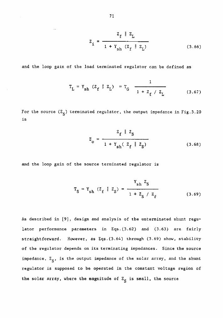
71
Zf H ZL
1 + Ysh (zf M zL) (3.66)
and the loop gain of the load terminated regulator can be defined as
1T = Y (z [ z ) = T ————————————
— L sh f L G1 + Zf / ZL (3.67)
For the source (ZS) terminated regulator, the output impedance in Fig.3.20
is
Zf H ZS
1 + YSh( zf M zs) (3.68)
and the loop gain of the source terminated regulator is
Ysh Zs
T = Y (z n z ) = ———————————-—S Sh f S
1 + Z / Z (3.69)S f
As described in [9], design and analysis of the unterminated shunt regu-
lator performance parameters in Eqs.(3.62) and (3.63) are fairly
straightforward. However, as Eqs.(3.64) through (3.69) show, stability
of the regulator depends on its terminating impedances. Since the source
impedance, ZS, is the output impedauce of the solar array, and the shunt
regulator is supposed to be operated in the constant Voltage region of
the solar array, where the magnitude of ZS is small, the source

„ 72
interaction is not as critical as the load interaction and is quite pre-
dictable using Eq.(3.69).
The load characteristics of the power conditioning equipment create
two areas of interaction concern in the stabilization of the shunt regu-
lator feedback loop. First, the resonance of the input filters required
the power conditioning equipment create a low impedance on the bus (ZL)
at the resonant frequency, which may cause an oscillation or an undesir-
able transient response. Secondly and more importantly, because the
typical load (equipment) for shunt regulator is (a) switching
regulator(s), the phase of the loop gain TL in Eq.(3.67) can be shifted
‘more than 160° when its magnitude is still greater than unity due to the
negative input impedance characteristic of the switching regulator. This
fact established the need to have the output impedance of the shunt reg-
ulator, ZB and the load impedance, ZL, well defined over the bandwidth
of the loop gain.
3.4.2 Modeling of the shunt regulator circuit
A block diagram of an existing shunt regulator as shown in Fig.3.2l
has been modeled in detail. The computer model takes into account salient
dynamics and nonlinearities including op-amp feedback, op-amp saturation
and darlington cut-off. All diodes, including the transistor‘s base—to-
emitter junction, have an infinite reverse impedance. The first order
model is used for transistors with their parameter values (such as current
gain and base-emitter junction Voltage,VBE)
as the user°s inputs. The
LC low-pass filter is added, which can be considered as the input filter

73
>U
EIN
—|
E
ü2
*¤
I'·—· EI
_-—‘.¤
“¤» ° 1 E
ÜN + > IU
0I 2
,. ___ | LL. I—¤
1~1N ¤_N I.*;·
+ ,I, QI :
I L"- +I '
E6** I '
I¤
I L1 2
I IE
I3
'_+•- I
L
N III C
IZ 31¤J '<
IE V7
1 §
II I.I.I ^;7I 7** °"
•- | I ä cuL
-1 L‘·—··—- 1 I ä__.¤
'“ ¢~
F vvS•- (N
S °I
>.¤•-
0
¥ . >a· >

74
and/or the cable impedance from the solar array to the shunt regulator.
It also allows preservation of the standard interconnection law providing
four terminal variables.
The analytical derivation of the transadmittance Ysh from Fig.3.2l
results
: _+
_Ysh [ Kl AS G1 G2 ] K2 K3 F (3 70)
where Kl is the sensed voltage divider factor, AS the error amplifier
transfer function, Gl and G2 the filter transfer functions, K2 the gain
from the base voltage of the darlington transistor to the base current
of the shunt elements, K3 the 12 sections of shunt elements, and F the
current gain of the shunt elements.
3.5 Filter / Cable Modeling
_ Spacecraft power components usually require both input and output
filters to decrease andiosusceptibility and to reduce switching current
ripple seen by the main bus. This is particularly important for switching
converters having pulsating input or output current. Power distribution
cables can also be realized in the filter model.
Fig.3.22 shows the single stage low pass filter configuration that can
be used for both filter and cable models. Other multiple stage filter
or n-section cable models can be constructed by cascading the model.
Parameter estimation can be quite difficult for a cable model. An at-

75
i1 1. i*‘ R! 1-L
+ +
Rv ° v1 R ZT
C
Figure 3.22 Single section of cable/fi/ter model

76
attractive modeling approach using empirical data modeling of such com-
ponents is discussed in Chapter 7. From Fig.3.22, the tw0·pOIt g-
parameters are derived as follows.
G = --1--·1 ZL
+Z1 Z1Z Z_Z (3,7.,L 1 2
whereZ1 = R2 + sL
22 = RT H ( RC + 1 1 sC )
3.6 Payload modeling
Due to the diversity of the spacecraft°s payloads, flexibility of the
modeling technique is very important. As described in Chapter 2, the
modeling techniques can use state equations, transfer functions, empir-
ical data, or a combination of these. For experimental data modeling,
the payload can be characterized by two types of data, frequency domain
and time domain. The frequency domain data can be further realized with
the analytical model by using the complex curve fitting technique. De-
tails of this approach are described in Chapter 7. The time-domain data
model can be obtained in tabular form when the payload is a time varying
function where the dependent variable is not directly a function of system
electrical operating conditions but of some external variables such as
temperature, light intensity, aging, etc.

77 ‘
3.7 Conclusions
In this chapter, components of spacecraft power systems are modeled.
Each component is described with the two-port hybrid g—parameters and its
interconnection law.
A component level analysis is performed by means of unterminated,
singly terminated (one-port), and doubly terminated (two-port) component.
The important performance parameters such as line transfer functions,
input and output impedances and feedback loop gains for regulators are
derived in analytical closed forms in which the terminating elements, ZS
and ZL are explicitly factored out. Based on the derivations in this
chapter, the system level analysis focusing on the subsystem interactions
can easily be carried out as will be shown in Chapter 6.

Chapter 4
MODELJNG A DIRECT ENERGY TRANSFER POWER SYSTEM WVTH EASY5
4.1 Introduction
Based on the component models generated in Chapter 3, a complete system
can be configured by interconnecting the component models. The particular
spacecraft power system under investigation is a direct energy transfer
power system [10] which is described in Section 4.2. In Section 4.3,
system model building with the host software EASY5 and its analysis ca-
pabilities are described. '
Using the system model generated in this chapter, the capabilities of
the model are demonstrated in Chapter 5 through Chapter 7, by performing
various types of the system level analysis.
4.2 Direct energy transfer spacecraft power system
The system being modeled in this study is a direct energy transfer
(DET) system whereby the primary power source, a solar array, is coupled
through a main distribution bus directly to the spacecraft electrical
loads. The various power-conditioning components, as shown in Fig. 4.1,
are activated only as needed, thus requiring the system to process only
the amount of power needed to maintain the bus at the specified voltage
level. A system mode of operation is determined by the power system
control unit. The control unit continuously monitors appropriate signals
to activate the power conditioning equipment. The control unit provides
78
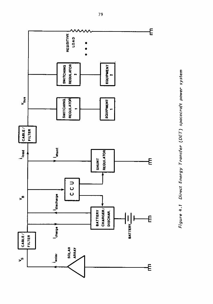
79
usEa’Z<*2o
•$.4E
••
oN g-
’
EE z:< W':D E"
q,
gg :4+.4
ÖV1
W AveL
··ä
:4 CDO
>° zä E Qzj ä
g__
gg" &•·°‘G
.%%:4 ä ö‘“ 8O
\
Q
nu:W
a'4'i' ~<d
|~
Qu. LuQ\-J
E ä¤=E; ¤Dg gi1:v>ä:‘
AOiE
D LEU T3
• L)q;
>° Q
_g
g Q2
..°D \v~
{Ed ¤~4u¤<pg:
GJ
p-(QL
<:Q3
• ¤o¤ > ¤s¤
N'“
hgg LL
\ lg.-
IHN §•-
a'4‘i‘’ ä
<;‘
Qu. N>-<<
W 2 O1
> 3 u4<I

80
signals that control the disposition of the solar array, battery and shunt
currents to maintain the bus Voltage regulation. When the bus Voltage
exceeds the specified level, the control signal activates the shunt reg-
ulator, and the excessive solar array power is absorbed by the shunt el-
ements. In this mode, the solar array also supplies the charging current
to the battery if it is necessary. When the bus Voltage becomes less than
the specified level, the battery discharging electronics are activated
and the load power is supplied by the solar array and the battery in
shared mode. The battery discharging current is controlled by the bus
Voltage.
In this study, modeling of the battery and the battery charging elec-
tronic are omitted, thus, the battery is treated as an ideal Voltage
source. A boost type switching regulator is used for the battery
discharger, which will be described in detail in Section 5.4. ~
The system modes of operation of the DET system are described in
Chapter 5. Since the system is configured by interconnection of various
components, complex interactions among components and subsystems may oc-
cur that can cause the total system to oscillate. In Chapter 6, Various
analyses are performed to demonstrate that the system can be unstable due
to the undesirable interactions among the individually well behaved com-
ponents.
4.3 EASY5 system model generation and analysis
Once all the necessary components are modeled, they are stored in EASY5
macro component library. As shown in Fig. 4.2, the EASY5 consists of two

8l
USER DEFINED STANDARDACRO COMPONEN FUNCTION
LIBRARY LIBRARY
MODEL MODELnsscmmoussusamouDATAPROGRAM
SYSTEM MODELSUBROUTINE
ANA Y ANALYSIS ANALYSISDUTÄISPROGRAM RESULTS
Figure 4.2 EA$Y5 system

82
programs, and a library of predefined Standard Components. Predefined
Standard component models include many of the common effects found in
dynamic systems such as standard analog and discrete controllers (pro-
portional, integral, differential, etc.) transfer functions, nonlinear-
ities (relay, saturation, hysteresis and switches), linear state equation
model, etc.
Model generation: The EASY5 Model Generation program uses a block
diagram type of approach for constructing various system models. All
interconnections between the component models are accomplished by the
Model Generation program according to the user specified Model De-
scription Data. This is accomplished by matching the input and output
port quantities of each interconnection. Table 4.1 shows the Model De-
scription Data of the DET system. The program also produces a complete
list of input data that is required by each component to complete the
model description. The scalar and vector parameters and tabular data
required for the analysis are included in this list.
Analysis: Once a system model has been constructed, the Analysis
program performs various dynamics analyses according to the user provided
Analysis Data. The Analysis Data includes parameter values, initial
conditions of states, various analysis controls and analysis commands.
Among the various analysis controls in EASY5, it is important to note that
the INTEGRAL control allows one to perform the analysis at various levels
such as system, subsystem, or component. The analysis in the component
or subsystem level is done by °freezing° the states of the subsystem of

83
#
* MODEL DESCRIPTION DATA OF THE DET SYSTEM«MACRO FILE NAME = DETI*MODEL DESCRIPTIONLOCATION = I, SA, INPUTS = FS(|I=I2)LOCATION = 2, FS, INPUTS = MCI(S2=|2)LOCATION = 22, SH, INPUTS = FS(V2=VI)LOCATION = MI, BA, INPUTS = DQ(|I=|2)LOCATION = M3, DO, INPUTS = BA(VG=VI), FS(V2=VC)LOCATION = 6, FD, INPUTS = FS(V2=VI), MC2(S,2=|2)LOCATION = II, MCI, INPUTS = SH(IH=SI), DQ(IL=S3),FD(II=SM)LOCATION = 54, FSI, INPUTS = SRI(II=I2), FD(V2=VI)LOCATION = 55, SRI, INPUTS = FSI(V2=VI), LOI(II=|2)LOCATION = 56, LOI, INPUTS = SRI(V2=VI)LOCATION = 57, FS2, INPUTS = SR2(II=I2), FD(V2=VI)LOCATION = 58, SR2, INPUTS = FS2(V2=VI), LO2(V2=VI)LOCATION = 59, LO2, INPUTS = SR2(V2=VI)LOCATION = 73, PT, INPUTS = FD(V2=VI)LOCATION = 63, MC2, INPUTS = FSI(II=SI), FS2(II=S3), PT(II=S¤)END OF MODELPRINT###**#**#***»»*uu**»##»#»«*#**#***#*###***»«#
* SA : SOLAR ARRAY
* SH : SHUNT REGULATOR
* BA Z BATTERY* DO : BATTERY DISCHARGER* FS : SINGLE STAGE FILTER
* FD : TWO STAGE FILTER
* SR : SWITCHING REGULATOR* LO : PAYLOAD
* PT : DIRECT LOAD* MC : SUMMER»
hä*§******#N#*{****#**#***#******#*********
Table 4.7 EA$Y5 Model Description Data of the DET system

84
little interest. This control feature is particularly useful when one
is interested in investigating behaviors of a component or a subsystem
in the presence of the entire system. A list of the analysis techniques
available through the Analysis program are given as follows.
•Time history generation - nonlinear
simulationl
•Linear model generation with eigenvalue and
eigenvector calculations
•Frequency response analysis
•Root locus calculation
•Steady state analysis
•Stability margin calculations
•Optimal controller synthesis

Chapter 5
ANALYSIS OF THE SOLAR ARRAY SYSTEM MODE OF OPERATION
5.1 Introduction
Solar arrays, as the primary power source for spacecraft, generates
its output electrical power relative to the illumination level. The op-
erating point of the solar arrays is determined by the power conditioning
equipment and the load characteristic. Secondary power conditioning
equipment consists of a shunt regulator, a battery bank and its charging
and discharging electronics. When the output power of the solar array
exceeds the load demand, a portion of the excess power is used to charge
the battery bank, the secondary power source, with a portion dissipated
in the shunt regulator. When the load power demand is higher than theh
solar array output power, the battery bank supplies the excessive load
power through the battery discharging electronics. The power condition-
ing equipment not only balances the power of the system, but also regu-
lates the bus Voltage. Since the solar array output power varies over a
wide range according to the changes in the illumination level, several
modes of operation exist depending on the characteristics of the solar
array, the power conditioning equipment, and the load.
As described in Section 3.3.2, the solar array output characteristic
is nonlinear. This nonlinear source coupled with nonlinear load charac-
teristics may result in multiple equilibrium points under a given oper-
ating condition. The actual equilibrium state that the system resides
85

86
on is determined by the stability nature of the equilibrium points and
the past history. Thus, it is necessary to analyze the stability of the
equilibrium points and to understand various modes of operation of the
system.
In Section 5.2, stability of the equilibrium points of a solar array
system with a nonlinear load characteristic is analyzed. The behavior of
different solar array operating points are plotted as trajectories on the
state plane. Stability and transient responses of the system operating
near the solar array maximum power point is considered in Section 5.3.
In Section 5.4, the operation during battery discharge is analyzed
including the transition mode from the shunt regulator active mode. In
the direct energy transfer (DET) system, the battery discharger directly
regulates the main bus voltage. Since the solar array output power varies
over a wide range, the battery discharge converter operates from no-load
to full load. Under light load, the converter operates in the discon-
tinuous conduction mode where the energy storage inductor current is re-
duced to zero during a portion of a switching cycle. The DC and dynamic
behaviors of a switching converter in the discontinuous conduction mode
are quite different than that of the continuous conduction mode. Modeling
of the discontinuous conduction mode employing the state space averaging
is described in Section 5.4. Since the battery discharger also functions
as the bus voltage regulator, the feedback compensator design for the
converter in both modes of operation are also discussed.
In Section 5.5, various modes of operation of the DET system are de-
scribed. Conclusions are presented in Section 5.5.

A87
5.2 Large signal behavior of the solar array operating point
Fig.5.l illustrates a solar array power system, in which the static
load line represents a typical buck type regulator load line character-
istic. The Voltage VR in the figure is the minimum solar array output
Voltage above which the converter is able to regulate its output Voltage.
When the converter is regulating, the solar array sees a constant power.
Note that the converter exhibits a negative resistance characteristic in
this mode. Below VR, the converter behaves as a resistive load to the
solar array.
As shown in Fig.5.l, there may exist three equilibrium points in the
system. The large signal behavior of a solar array operating point de-
pends on the stability nature of each equilibrium point. The qualitative
large signal analysis can be carried out by considering a second order
system shown in Fig.5.2. The solar array output and the load character-
istics are replaced by the nonlinear functions and the LC low—pass filter
in the model represents actual physical elements in the system such as
an input filter of the switching regulator or the cable impedance between
the solar array and the load.
Let us first consider the stability nature of each equilibrium point.
Defining the states x = [iL vC]T,the system state equations are
&=i(v-v)=i(-f(i)·v) (51)dt L S C L L C '
&=-}—(i·i)=L(—f(v)·i) (52)dt C L R C C L °

88
I Reglon #1 I Region #2 I Region #3IIpal pezI
pe:LOAD
Vn V
Figure 5.1 Representation of a solar array power systemwith a switching regulator load line ‘
II.
I
ms)
I
ttvcz
Is Vc
Figure 5.2 Equivalent circuit model of the system in Fig.5.1including LC filter

89
where vs and iR are defined in Fig.5.2.
From Eqs.(5.l) and (5.2), the equilibrium points in Fig.5.2 are
Vc = 'HIL) ‘(5.3)
IL = f(VC) (5.4)
The behavior of the trajectories in the neighborhood of an equilibrium
point can be found by linearizing Eqs.(5.l) and (5.2) about an equilibrium
point. The nature of these equilibrium points is analyzed by introducing
small perturbations about the equilibrium points.
ir. = 11.+12 (5.5)
vc = VC + vc (5.6)
where IL and VC represent the steady state quantities, and il and vc are
the small signal perturbations.
Substituting Eqs.(5.5) and (5.6) into (5.1) and (5.2) results in
diL 1—-— = —— [ -f(I + i ) - ( V + v ) ] (5.7)dt L L 2 C c
dvc 1——— = —— [ -f(V + v ) — ( I + i ) ] (5.8)dt C C c L 2

90
Expanding Eqs.(5.7) and (5.8) in a Taylor series about the equilibrium
points, the equations of the first order approximation are
f(IL + ig) = f(IL) + rs iz (5.9)
where~
I =f(1L)
Sdi_ L IL
and similarly,
1f(VC + vc) = f(VC) +·;; vc (5.10)
where”
1 df(vC)
I
T: TTL dvC VC
where rs and rL are the incremental resistances (tangential slope) of the
solar array output curve and the load line, respectively, at the equi-
librium points.
Employing Eqs.(5.3) through (5.10), Eqs.(5.7) and (5.8) can be simplified
as
dil ( 1/L ) ( -rS iz - vc )
dv}; (1/C ) ( iz ' (1/rr.) VC) (5.11)

91
Note that the value of rs is the same as the output resistance at a point
on the solar array I-V curve as derived in Eq.(3.60). The system
eigenvalues are expressed as
X X =1 Is 1 rS 1 4 rS
é (5.12)1’2 —' ·(—+——)+[(—+—·)“·—(l+—)]
2 L rLC L rLC LC rL
From Eq.(5.12), the stability of each equilibrium point can be determined
for given parameter values. For the load line shown in Fig.5.1, the
following results are observed.
In Region #1: rL > 0
The equilibrium point,Pel
is stable and is either "node" (real) or
"focus" (complex).
In Region #2: rL < 0, |rS| < |rL|
X1 and X2 are both real but of opposite sign, and Point Paz is a
"saddle" and is unstable.
In Region #3: rL < 0, |rS| < |rL|
The stability of Point Pe3 depends on the parameter values.
Since the normal mode of operation should be in Region #3, the values of
L and C in Fig.5.2 must be chosen to provide the stable equilibrium points
in this region and to allow further analysis. However, it must be noted

92
that the equilibrium points in Region #1 are always stable and those in
region #2 are always unstable (saddle points) regardless of the parameter
values. The value of rs for each equilibrium point can be obtained using
Eq.(3.49). The value of rL in the constant power region is
övc PCrL = =-«
. 2 ,= -Sir VC, IR ir ir IR (5.13)
Approximate values of rs and rL can be found simply by drawing tangential
slopes to the solar array I—V curve and load line, respectively, for each
equilibrium point.
To construct a state plane trajectory the isoclines for each equilib-
rium point are derived using Eq.(5.11).
diz 1——— = O —• il = -·—— vcdvc rs (5.14)
dig 1Ä -> „ _)
: VC
dvc rL (5.15)
The results in Eqs.(5.14) and (5.15) are the tangential slopes to the
source and load curve at each equilibrium point, thus the trajectories
cross the solar array curve horizontally and the load line vertically.
Near the equilibrium points which have real eigenvalues, the trajectories

93
follow the slope of the eigenvectors of the system, K.
X X =L rs 1 rs 1 4 1, (5.16)
1’2 —'—(·—··—)+[(—·—)“·—]2 L rLC L rLC LC
Using the above results, the state plane trajectories can be sketched.
Fig.5.3 illustrates the trajectories for the case where the equilibrium
pointPaß
is a stable node. As shown in the figure, the trajectories are
separated by the separatrix that has the slope K2 at Pez. The two
starting points Pl and P2 in Fig 5.3 approach. two entirely different
steady states, even though the initial states differ by only a small
amount.
For the solar array model used in this study the following cases are
set up for the computer simulations. As mentioned above, if we assume
that point PG3 in Region #3 is stable then there can be four possible
cases:
i) Pel - node, P63 — node
ii) Pel - node, PQ3 - focus
iii) Pel - focus, Pe3 - node
iv) Pel - focus, Peg - focus
However, investigation of the cases i) and ii) are sufficient to under-
stand the behaviors of the system. The results from simulating these

94
_ /SEPARATRIX _I L #1 #2 #3 1
I II \ [I 1\ 1
7 I I
”“2...-----1 P °‘
„ [ s2[Ü
~„\ I I \~
I I\1
1 [‘
I ‘ \[
Q I I '‘
pasISOCLINE , \
'71--- --[ 1
I 1 'I 1I‘,
g 1\ 1\ I
VRvc
Figure 5.3 St¤te—p/cme tra/ectories of the system in Fig.5.2
95
cases are shown in Fig.5.4a and 5.4b given the following system operating
conditions.
The solar array short circuit current,ISS,
is 45.4lA, the open circuit
voltage, VGC, is 32.0V, and the maximum power is 1050 watts. The constant
power load line is set to 850 watts, and the boundary of Region #1 and
#2, VR, is 15V. The values of rs and rL at the equilibrium points in each
region are listed in the following table.
Pel Pe2 Pe3
IL 45.38 45.02 30.34
VC 12.03 17.31 28.02
rs 64.92 37.3 0.20
rL 0.025 -0.56 -1.47
The cases i) (Pe3 node) and ii) (P63 focus) are shown in Fig.5.4a and
5.4b. The eigenvalues and the slope of the eigenvectors for the partic-
ular values of L and C are listed in the figure. In Fig.5.4, the
separatrix is clearly illustrated. It is obtained by adjusting the ini-
tial condition that is located near the line which has been estimated from
information about X2 at Paz. The trajectories from the initial points
in the left-hand side of the separatrix (Pl through P6) converge to Pel,
and those in the right-hand side of the separatrix (P7 through P12)to
Peg.
Since in Region #1 the system bus voltage is not regulated, the de-
sirable mode of operation should be in Region #3. This implies that there

96
0C?C)LD
I( 1
P P /\ :6 5 //_ \ Q : P12 P11
CD \\<1· — — - -
7/ E\x \ \
.‘~
x/ 1 \
¤ \ui [
' x \cn 1 1 °10
/ xZ] / 1 V x0 I '. 7 1 \ \
\ °N 1g[1{ \
1 ' \I E
A] 1 : \
1l E
\.O
l' P7 P2P3‘=
P7 P8 1 9O ·¤C)
0.00 8.00 18.00 24.00 32.00 40.00
VC
Figure 5.40 Simulation of state·plane tra/ectories for thecase where the equilibrium point Peg is ’stab/e node'
(L = 70 1.1H, C = 500 pF)

97
C)C?OLD 1
II’\EP6 P6 / \P1 ' P12 P11
aj /sr —-— —
' Wgl \6 ' 1dj / Ä \ P10m / 11
.1 / Ä Ä
3 1 \§ / I \
/,1
\1 \\
OP1
C2 / ·
l IO \
O0.00 6.00 16.00 24.00 32.00 40.00
VC
Figure 5.4b Simulation of state—plane tra/ectories for thecase where the equilibrium point Peg is 'stable focus'
(L = 30 1.1H, C = 500 1,1F)

98
needs to limiting mechanism that prevents the operating point from set-
tling into Region #1 or a triggering method to move it to Region #3 even
if the operating point starts in Region #1. The limiting mechanism, by
means of battery will be described in the following section. A triggering
method is illustrated as follows.
Suppose that the operating point is at rest in Region #1. One way to
move this operating point into Region #3 is to decrease the load power
below the solar array curve so that the only one desired equilibrium point
exists. For the load line shown in Fig. 5.5, the equilibrium points as-
sociated with Region #1 and #2 have moved outside these regions, so that
they no longer exist. However, the behavior of the state trajectories
can be still seen by defining virtual equilibrium points, Pel'and Paz',
for which the slopes of the eigenvectors are also sketched.
Fig.5.6 shows the simulation result using the previous system for the
case i). In Fig.5.6a, the trajectory starts from an arbitrary initial
point, Pl and moves to P2 for a load power of 800 watts (Curve #1). As
the load power continuously decreases, the operating point moves along
the solar array curve until it reaches Curve #2. Further decrease in the
load power beyond this point moves the operating point from P3 to P4, then
to P5 for Curve #3. Fig.5.6b shows the time history of vc corresponding
the trajectory from Pl to P5. The above stability analysis for the system
in Fig.5.2 can be extended to following cases.
“System in the battery discharging mode: Fig.5.7 illustrates the
system in the battery discharging mode of operation. As it will be

99
' I#1 I #2 #5„ I: 'II \" PQI
:I
ä‘=
I Pe?.,___Vc
Figure 5.5 A trajectory from the initial operating pointin Region #1 to Region #2

100
C)C2Q I
co I
IO22*2 _ _ P2 IPs _
IB O22‘°I(TJ
I·’I"' 8
4 I_ N
II Ih
8 II p I # 1.6; I I ,” .// 1 SI #2/ I I #2
S I°0.00 6.00 18.00 24.00 62.00 40.00
VC
89 “P66 6 VIE
> 8 F1IIP2
6’I
°0.00 1.00 2.00 3.00 4.00 6.00TIME '“‘°°
Figure 5.6 Simulation of the triggering method from theundesired stable region to the desired region(a) state-p/ane trajectory(b) time history of the bus vo/tage

101
described in detail in the following section, the battery discharging
current can be expressed as a function of the bus Voltage with an output
admittance, 1/rB. The state equations are then,
diL 1——— = —— ( -f(iL) · VC ) (5.17)dt L
dvc 1 1·——— = —— ( i -
—— v - f(v ) ) (5.18)dt C L rB C C
Following the same procedures as in the previous derivations, the state
equations near the equilibrium point are
diz ( 1/L ) ( -rS ig - vc )
dvc ( 1/C ) [ ig · [(1/rL)+(1/rB)] VC ] (5-19)
Then the eigenvalues are obtained as
x Ä =T Ts 1 Ts 1 a Ts
é (5.20)l’2 — '(*+*)+[(*+——)2"*‘(l+—)]
2 L rEC L rEC LC rE
where
TE = TL H TB
Comparing Eqs.(5.12) and (5.20), the additional term, 1/rB, stabilizes
the system, and this can be explained as the system is operating on the

102
i E iL S RJ'
Ü .V X
ref
Figure 5.7 Simplified block diagram of the system in Fig.5.2with the shunt regu/ator or the battery discharger
{Ysh : for shunt modeQ :
x7/rB : for battery discharge mode

103
stiff voltage source line.
System in the shunt mode: Fig.5.7 also can be used to illustrate
the system in the shunt mode of operation. In this mode of operation,
Eqs.(5.l7) and (5.18) are valid if the 1/rB term is replaced by the shunt
transadmittance, Ysh. Fig.5.8 shows the state plane trajectories and the
time history of the states, with and without the shunt regulator. lt
clearly shows the effect of the additional term described above such that
the system without the shunt regulator is quite oscillatory while that
with the shunt regulator has faster responses and the system appears to
have real valued eigenvalues.
5.3 Analysis of the system operating near the solar array maximum
power point.
To utilize the maximum available power from the solar array, several
approaches were proposed in [11] and [12] to place the operating point
as close to the solar array maximum power point as possible. However,
near the solar array maximum power point, the dynamic resistance of the
solar array is very sensitive to changes in the operating condition and,
consequently, may result in system open loop instability.
To derive the solar array maximum power point, one can differentiate
the constant power load line, Pa = VI, and set it to zero.
3Pa BI—=V—+I=0 (5.21)BV BV

104
83
8:
83
.|
823
81
8m10.00 16.00 22.00 28.® 34.00 40.00
vc 6ui
$ W
8_-g 82
82’“IIIII>
'
" ' ‘. IIIIIIa0.®
Lw 2.® 3.w 4.CD 5.üJ
nmz 6
Figure 5.8 Comparison in the system response with and without the shunt
•-•—•-• .' with Shu/‘Ii'-——- : without shunt

105
V 3V—=·——
(5.22)I 8I
Eq.(5.22) states that at the maximum power point, the constant power load
line, RL, is equal to the dynamic output resistance of the solar array,
Ro, as shown in Fig.S.9.
To analyze the behavior of an equilibrium point, one can use the solar
array small signal model depicted by Eq.(3.5). One of the system
eigenvalues at the equilibrium point is
1,
Ceq ( 1 + Req / IL )(5.23)
where C and R are defined in Eq.(3.6l).eq eq
From Eq.(5.23) , for rL < 0, the system is:
stable if |R€q| < |RL|, and
unstable if |Req| > IRLIl
Here,Req represents the characteristic of the solar array output re-
sistance rs in Eq.(5.9).
In the stable region but near the maximum power point, M, the magni-
tudes of rs and rL are close together, and the eigenvalue is close to the
origin, which implies very poor transient response and stability margin.

106
Is\ ‘,
Constant Power°~_Load Line, P¤=V|‘s
MQ1.
~“"'!
ss
s sss
ss
sQO = QL
V
Figure 5.9 Relationships of solar array characteristic and constantpower load line at the maximum power point, M

107
In this respect it is desirable to operate the system in a region where
|rS| << |rL|. This can be seen from the step transient response simu-
lation using the system model developed in Section 5.2 (Fig.5.2). Fig.l0a
shows the response of the step change in the load power from 800 watts
to 790 watts, and Fig.5.l0b from 1040 watts to 1030 watts which is close
to the maximum power point (1050 watt). Therefore, to design a controller
to utilize the maximum available power from the solar array, one must take
into consideration of the stability of the operating point and the tran-
sient behavior of the system. One way to overcome this problem is to
perhaps use the shunt regulator to dissipate some solar array power. In
this mode of operation, the system can be stabilized as shown in Section
5.2.
5.4 Analysis of the solar array system in the battery discharge mode.
The basic functional requirement of the battery discharger is to reg-
ulate the bus voltage when the solar array is incapable of meeting the
load demand. In this mode both the solar array and the battery function,
as power sources. Fig.5.ll shows the system operating in the battery
discharge mode. When the bus voltage drops below a certain magnitude,
the control signal activates the battery discharge converter in order to
maintain regulation of the bus voltage. The solar array then supplies
the current corresponding to this regulated bus voltage.
In the DET system, when the solar array output power decreases due to
the weakening of the illumination level, the battery discharger operates
from no-load condition through the converter discontinuous conduction
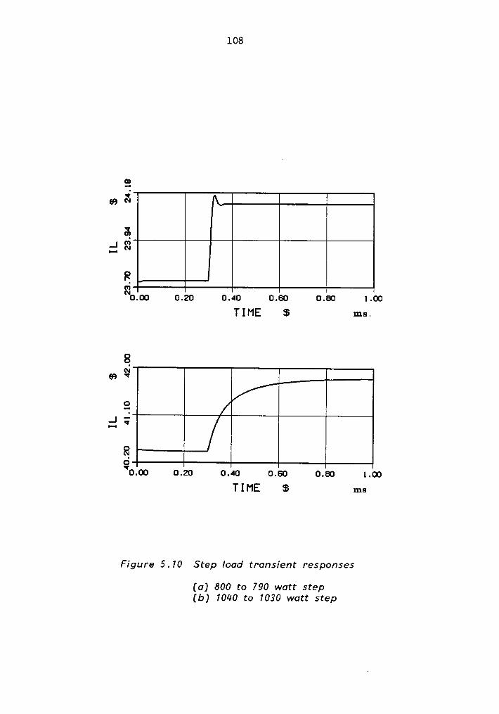
108
2Q lt]
8j Ü
8E30.00 0.20 0.40 0.60 0.60 1.00
TIME $ ms.
.N
Q V
2;¤ 9
890.w 0.20 0.40 0. 0.80 Lw
TIME $ ms
Figure 5.70 Step load transient responses
(a) 800 to 790 watt stepfb) 7040 to 7030 watt step

109
'sa 's „
BATTERY
soma ¤•scaAa6Ea T vbmeryAaaAv T
CONVERTER
vc
"„«E
Figure 5.77 System in the battery discharge mode

110
mode (DCM) of operation and ultimately to the continuous conduction mode
(CCM). Since the dc and ac dynamic behaviors of switching regulators for
the two modes of operation are quite different, the analysis and the
feedback controller design must take into consideration the two modes of
operation.
A particular battery discharge switching converter power stage used
in the DET system is shown in Fig.5.l2. The circuit basically operates
as a buck type regulator operating in push-pull mode. Since the terminal
Voltage of the battery is between 17 and 25 volts, an auto-transformer
is used to boost the Voltage to 28V. In this study, a simplified circuit
is used as shown in Fig.5.13a. The two sources in Fig.5.l3a represent
the transformer action between the power switches ON and OFF intervals.
The state space averaging technique is employed to analyze the con-
verter in the discontinuous conduction mode. As illustrated in Fig.3.2,
there exist three intervals d1TS, d2TS and d3TS. While the first inter-
Val, dlTS, (inductor charging) is dictated by the "ON" time of the
switching function and is a known quantity, the second interval, d2TS,
(inductor discharging) is yet unknown and depends in general on both the
length of the first interval and circuit parameters. However, d2TS can
be determined using the additional constraint in the discontinuous con-
duction mode described in Eqs.(3.S) and (3.6)
While the state space expression in Eq.(3.8) was sufficient to describe
the converter operating in continuous conduction mode, in discontinuous
conduction mode, the state equations for the three switched intervals in

lll
UIE
c0LL:>U 0
W
*6 S2, va:»
O
7:3
N ¤> 8c E °¤
S Sä
tcll:>¤ 8*5 S.‘: ¤;
L.- Ä 3o A U-2‘¤>«L0
+-0$0csLD
2L4
II °- ‘”LG 3ELL
+ ea I.¤
>

112
R3, L
+Vg 1 RC
60)C Vbus
I<Vg ;
I
:61
L L |_
[*+•<]V ; c% R% v .1 c% R} ; Ré
6, TS d2TS 63 TS
cb)
Figure 5.73 (0) Simplified circuit of the converter in Fig.5.72
(b) Three switched circuits

‘ 113
Eq.(3.8) do not describe the switching converter completely. Namely, the
instantaneous inductor current is restricted in its evolution such that
i(O) = i[(dl+d2)TS] = 0
i(t) = 0 for interval d3TS (5.24)
The state equations of Eq.(3.8) together with Eq.(5.24) completely de-
termine the behavior of the switching converter. Using ideal elements
in the circuit in Fig.S.l3a and ignoring load dynamics, three switched
networks in the discontinuous conduction mode are shown in Fig.5.l3b.
For the choice of the state vector x = [i v]T, the state space equations
of the three switched networks becomes:
x = A x + B v for interval d T1 1 g 1 s
x = Azx + Bzvg for interval d2TS (5.25)
x = A3x + B3vg for interval d3TS
where
0 _ l_ O 0Al=A2= L A3=
1- 1. 0 - Ä.
C CR CRl

114
(1+x) fiBl = L B2 = L B3 = 0
0 0 (5.26)D D
In addition to this,
imaxi = -—-- (5.27)
2
Eqs.(5.2S) and (5.27) contain all that is needed to determine both dc and
ac small signal models. Let us first consider the steady state (dc)
model.
Steady state (dc} model analysis
Averaging Eq.(5.26), the following linear algebraic static equations
result.
0 — Dl+D2 I Dl(1+¤)+nD2L
+L V = 0
8D1+D2- .i V 0 (5.28)
C CR
A • X + B · V = 08
Then the steady state solution of Eq.(5.28) is

115
EL E M =Dl(1+k) + kD2
Vg D1 + D2
V lI =——- (5.29)R (D1 + D2)
Hence, the dc conditions depend not only on D1 and R, as in the continuous
conduction mode, but also on D2. By use of the additional constraint in
the average of inductor current for (D1+D2)TS,
(1+k)V - V1 = li. D1Ts (6.60)
2L
the dc conditions are completely determined with the known quantities D1
and R. For example, substitution of Eq.(5.30) into Eq.(S.28) results in
1 KTn KTH é=__ ____ ____ zD22
(D1
D1 ) + [(D1 D1 ) + 4tn(1+k)] (5.31)
where
tn E 2L / (R TS) ; normalized time constant.
The boundary condition between the two conduction modes is
D2 < 1 — D1 ; discontinuous conduction mode
D2 > 1 - D1 ; continuous conduction mode (5.32)

. 116
Using Eqs.(5.3l), the critical Value of In can be determined by solving
D2=l-D1.
1 · D1Incrit =
l + ¤ + ¤(l - D1)/D1(5'33)
Suppose now that the output Voltage is regulated with some proper feedback
circuit, then the dc Voltage gain M can be treated as a constant for a
fixed input Voltage. The duty ratio, D1, in the discontinuous conduction
mode can be derived as a function of M, or as a function of tn.
tnM(M-x) QD1 = ————--- (5.34)
1 + ¤ - M
Using the results in Eqs.(5.29) through (5.34), the dc behavior of the
battery discharger is illustrated in Fig.5.l4. In Fig.5.14a, the boundary
condition, tncrit, between the two modes is plotted as a function of D1.
The dc Voltage gain, M, as function of D1 for different Values of Tn is
shown in Fig.5.l4b.
Since the battery discharger operates from no-load condition to full-
load, it is important to understand the start-up behavior of the con-
verter. Suppose now that the solar array output power gradually
decreases. lnitially the battery discharging current is zero (i.e., tn=0)
and the duty ratio D1=0. As the solar array output power decreases, the
operating point moves along the solar array curve which causes the bus

117
Ä
N
3N
*6l¤1
”
6
6D
6°0.01 0.21 0.41 0. >• 0.83 1.113
Ä
*6’
1.46
nb: 1EE..!
*6 .D
@[7°0.00 0.20 0.40 0.00 0.00 1.00
Figure 5.74 DC characteristics of the battery discharger converter
(0) Tncrit Vs D7
(b) M vs D1

118
Voltage to drop, thus activating the battery discharger electronics via
an error amplifier. In this start—up mode, it is very important to design
a proper error amplifier circuit for the following reasons.
For the high gain controller, since the sensitivity of the dc Voltage
gain with respect to the duty ratio is Very high as shown in Fig.5.l4b,
any delay in the logic circuitry or the false triggering due to the noise
will cause a high frequency oscillation in the bus Voltage. While in a
low feedback gain system the controller may not act fast enough to regu-
late the bus Voltage, since the plant time constant of the output
capacitor and load resistance is Very slow. This may cause a large am-
plitude, low frequency oscillation It is especially critical when the
output Voltage of the battery discharger converter is set such that its
operation is close to the solar array maximum power point. Since the low
gain controller allows the bus Voltage to drop before the controller
starts correcting the error, it is possible that the system may move into
the unstable region as discussed previously. Another important concern
when designing the error amplifiers is that, since the battery discharger
operates from the discontinuous conduction mode to continuous conduction
mode, the error amplifier should be able to stabilize the system in both
modes. Thus, it is necessary to analyze the dynamic behavior of the
converter in the discontinuous conduction mode.
l

119
Small-signal analysis: Perturbation and linearization of the averaged
equations of (5.25) and (5.27) result in the following ac dynamic model.
E 0=L + L vg
G Dl+D2 _ —l G 0C CR .
l(1+¤)V - V ¤Vg - V-—-g- ^ —-— ^ (6 35)+ L dl + L d2
I IC C
with additional constraints
E=0 ($.66)dt
I A (1+x)I A I Ai=—d+———l——v -—l——-v (5.37)1+ V - V 1+ V — VD ( •<)g g ( •<> 8.
Substituting the additional constraints from Eqs.(5.36) and (5.37) into
Eq.(5.35), the unknown modulation quantities dz and i can be determined
in terms of other known dc and ac quantities. Thus, the complete dynamic
model can be expressed as

120
dv 1 (2M-K)-(K-M): AC —— = -
———————————— vdt R (1+:-M)(K-M)
M MD2+Dl+:Dl^+ — —————-—-—*l-—- v
R (l+¤-M)(x-M)(Dl+D2) 8
_ _ (5.38)V
(D1+D2)(¤ M) D1A
+ —— —————-———————— dlR Dl(Dl+D2)(x—M)
It is now easy to obtain from (5.38) the two transfer functions of in-
terest
i : G -———-D
G og 1 + S/W (5.39)8 P
i : G —-—M
al od 1 + S/wp (5.40)
where
G = 5.41og M ( )
(D1-(D1+D2)(x—M))(l+¤·M)G =V (5.42)
od- - - 2D1(Dl+D2)((2M m) (K M) )
1 (K-M)! - (2M—n)w = —— ————— (5.43)
p RC (1+x-M)(¤-M)

121
The transfer function models are rather complicated for this particular
converter circuit, however, they are expressed in terms of well defined
constants which can easily be calculated. The qualitative interpreta-
tions of the results are as follows.
Eqs.(5.39) and (5.40) show that the transfer functions have a single
pole and no zero. Due to the additional constraint in Eq.(5.36), any
converter that can be described with two state variables of which one is
an inductor current, has a single pole system transfer functions in the
discontinuous conduction mode. Thus, the dynamic behavior of the con-
verter operating in the discontinuous conduction mode is completely dif-
ferent from that of the continuous conduction mode, in which the system
has a complex pole pair. Therefore, the feedback controller should com-
pensate the plant dynamics in both modes of operation. This is clearly
illustrated in the root locus diagram of the open loop converter as a
function of the load resistance in Fig.5.1S. Without a compensator, the
system eigenvalue is close to the origin, thus the system response should
be very slow in the discontinuous conduction mode as intuitively predicted
in the dc analysis. Decreasing the load resistance beyond Rcrit, the
converter will operate in the continuous conduction mode, and the open
loop eigenvalues become complex. In this range, the response is still
slow and oscillatory. A further decrease of the load resistance will move
the locus onto the circle with the radius of wo = /EÜ, and finally the
locus approaches to the real axis again.

122
IMAGINARY
/•
{•
/ ', I
/ {‘I
/l—·•··-
CCM II/ :° R=|R[CYII R__„
• Ol • •; • •[ R—·0 REAL
· {\ I
I, I-
II•I
X II• I
• :• I%••-I
Figure 5.75 Root locus of the open loop buck—type converter as0 function of lo0d resistonce, R for DCM 0nd CCM


124
DCM I CCM7>%1
L1
c c c H c ° Ä hc EC C ilkc
(c) C
Figure 5.76 Root loci of the closed loop buck-type converterin DCM and CCM for three compensators
(a) proportional gain(b) integrator plus /ead—/ag(c) proportional plus /ead—lag
XC .° COfT7p€f7$GÜOl7 pole
Qc.‘
COmp€l7$C7ÜOf7 Z€l'O

125
In order to verify the above analysis and to observe the effect of the
integrator in the DCM, the DET system is simulated employing the
compensators shown in Fig.5.17. Fig.5.18 shows the step load transient
response (from 1300W to 1400W) of the system when the battery discharger
operates in the continuous conduction mode. As shown in the figure, the
system behaves equally well for both compensators. In Fig.5.19, the load
power (iload) is gradually increasing and various modes are illustrated.
The system initially operates in the shunt mode until 0.6 ms, then it gets
into the dead band mode where the solar array solely supplies the load
power. The operating point moves along the solar array curve as the load
‘power increases. The battery discharger employing the compensator with
the proportional gain (Fig.S.l6c) starts regulating the bus voltage at
t=lms as shown in Fig.5.19a. While that using the integrator starts to
operate at t=2ms and slowly increases to the regulation voltage as shown
in Fig.5.19b. As shown in this figure, the slow response in DCM of the
integrator type controller may cause the bus voltage to drop out of the
regulation range.
The results in Figs.5.l6 and 5.19 show that a compensator designed for
CCM mode of operation may not be suitable for DCM mode of operation, and
consequently, may result in a bus voltage oscillation or large voltage
droop due to a load transient. Design of a compensator for the boost or
buck-boost type converter must be done more carefully. This is because
such converters also have a single pole in the discontinuous conduction
mode, but, in the continuous conduction mode, there are a complex pole
pair and a right·half plane zero.

126
GAIN _ _COI11p€|"•S¤fO|' In Flg, 5.|6bIDBI
x wP1‘
E\ :\
\wzl mz E
x ;
Compensctor In Fig.6.I6c
, FREQUENCY
Figure 5.77 Two compensators used for the simulation
. Power stage : wo = 3000 in CCM0 < wp < 72.4 in DCM
Compensator : wli = 7000
wz, = 6000
wp, = 50000

127
6 1 8E N vvg E
IIIIIIIIII„ E 6¤ < 1-3 " '2II
I- I-8 UG
; ö Ef
* L2 $,01IILIHIII 6 U lim6 E .6-E
Ih ct
8 6600*62 SL°l.Z 06*1266 00*6v 00*16 00*62 00*61 00*01 gg LL
O
6 SFISA 6 1N3aan:1 j —§;
- 3 E?.
8 ä äg1 "' b 81:
3 66I 8 6 ff.; 3
6°€
36II •-L U3IJ
¤ E E Ü E< -* 1- E 3O O ( ci
..'I •-In ...¤1I ö<
I I 6
III IIIIIIII 800*62 61*12 06*1266 00*611 00*16 00*62 00*61 00*01°
S SOSA S .LN3&lHI'I3

128
3
IEIIEI_ . 8E cn*-2N
" Ot
2 ·’ · 8IF N S¤ 2 E ää
- §Us8 _g Fa:. 5 _:
; °°é’:>
E iiä +-2 og" 2 fi
ä'8Z SS'LZ ®'LZ'SV CD°ä ®°LZ (IVG! ®°6®'Ossnsm s maaana ‘— 9,-E
E ss8 Ä 88
•GJ‘
' g ff3 ¤>¤s
z’
6 va 225 E ^"3 U; if,
„ E "' g,E Ä ä E
u3* *IHIII
OI-ZD
°' 3Iä1II 2$°8Z SS°l.Z ®'LZ SV ®'$ ®°LZ ®'8| ®'6 ®°0°
snazx maaanzs

129
5.5 Analysis of the solar array system modes of operation
The modes of operation of the DET system is described in this section.
In Fig.4.l the Central Control Unit (CCU) continuously monitors the bus
voltage and commands the system to operate in the battery discharging mode
when vbus is less than Vrb or in the shunt active mode when vbus is greater
than Vrs. When vbus is between Vrb and Vrs, there exists a "dead band" l
at which the load power is equal to solar array output power. When the
system operates in the shunt active mode, any variation of the bus voltage
generates a proportional shunt current, ish. The shunt current together
with the load current sinks the solar array current and regulates the bus
voltage. When the system operates in the battery discharge mode, the bus
voltage is regulated by the battery discharger. The solar array current
is set by the bus voltage on its output I-V curve and the battery dis-
charging current is the difference between the solar array current and
the load current.
The system operating condition is subject to change due to constantly
varying load power consumption and the solar array power generations.
The entire DET system shown in Fig.4.1 is simulated to observe how the
system operating point moves from one mode to another. Fig.S.20 illus-
trates the case in which the solar array I-V characteristic varies ac-
cording to the illumination level. In this example, the illumination
level is set to be linearly time varying from Curve #1 (shunt active mode)
to Curve #4 (battery discharging mode) as illustrated in Fig.5.20.

130
#1FA
/ \Vrb Vrs V
Figure 5.20 DET system mode of operation for the solar arrayillumination level changes

131
From Fig.5.20 and the simulation result in Fig.S.21, the system mode
of operation is described as follows: Starting from Curve #1 and the
corresponding operating point A, the operating point travels along the
shunt regulation line, VIS until the solar array power decreases to Curve
#2. In this mode, the shunt regulator is active and it absorbs the ex-
cessive current generated by the solar array through the shunt elements
(ish). Between Curve #2 and #3 the dead band mode exists where both the
shunt regulator and battery discharger are deactivated. Thus, the oper-
ating point travels along the load line from point B to C. Further de-
crease in the illumination level activates the battery discharger. The
operating point then follows the battery discharger regulation line, Vrb.
In this mode, the load power is supplied by the solar array and the bat-
tery.
Fig.5.22 illustrates the case where the load power is varying while
the solar array I-V curve is fixed. With the solar array curve fixed and
the load line below Curve #2, the operating point is set at Point A. As
the load power increases beyond Curve #2, the shunt regulator is deacti-
vated, and the operating point travels on the solar array curve until
Point B. Further increase in the load power beyond Curve #3 activates
the battery discharger, and the operating point moves along the battery
discharger regulation line to Point C.

132
6Z N265 3D:1*‘ 8
O
a
88 8 BI: 8Q ' III
D ß '(DQ<¢g11
Q(8 I-88888IIIQ I EELI6Z
·
LU ^Q QIIIID
P8 .8 8 8 8 II AQI VI°0.® O.® l.60 2.40 3.20 4.®
TIME ms
Figure 5.27 Simulation of the DET system for the so/ar arrayillumination changes in Fig.5.2O

133
I #4 5 5
#3#1
1.oAo muss
i \Vrb vrs V
Figure 5.22 DET system mode of operation for the load power changes

134
5.6 Conclusions
ln this chapter, various solar array system modes of operation in the
large signal sense are analyzed using the state plane method. The anal-
ysis shows that any equilibrium point in Region #2 of Fig.5.1 is unstable
with real eigenvalues. The state plane trajectories are separated by the
separatrix that passes through Region #2 and converges to either of the
two stable equilibrium points in Region #1 or #3. Thus the behavior of
the system is quite different on either sides of the separatrix. Since
only the equilibrium point in Region #3 is the desirable operating point,
a control method to move the operating point from Region #1 to Region #3
is discussed. The analysis also provides a guide line for the system
initial start-up condition that leads to the desired mode of operation.
The behavior of the operating point near the solar array maximum power
point is analyzed. As far as stability and transient response are con-
cerned, the equilibrium points near the maximum power point, in general,
are less commendable than in the region where the magnitude of the solar
array output resistance is small, or in the range of a stiffer Voltage
source.
Since the battery discharger in the DET system operates from the no-
load condition through the discontinuous conduction mode (DCM) to the
continuous conduction mode (CCM), the feedback compensator must be de-
signed carefully to ensure stability in both modes of operation. Various
compensators are compared. The results show that a proportional gain
control is most appropriate for the converter operating in the discon-

135
tinuous conduction mode. It not only speeds up the system response but
also prevents system oscillation near the no—load condition. In the CCM
mode of operation, a phase lead type compensator is required to compensate
the excessive phase lag due to the complex pole.
The solar array system modes of operation including the shunt regula-
tor, battery and switching regulator load are described. The entire DET
system is simulated for a continuously varying illumination level and the
behavior of the system in various modes of operation are observed.

Chapter 6
SUBSYSTEM INTERACTION ANALYSIS
6.1 Introduction
One of the major difficulties in large scale system analysis involves
the subsystem interaction problems. As a system becomes more complex,
the interaction problems create a large degree of uncertainties to the
system response even though each component may be well understood and
documented. Thus, the total system analysis must include the interaction
analysis that allows one to predict the system level responses and to
trouble-shoot the system. The interaction analysis also provides design
information of a component or subsystem at the initial design phase and
for the future modification of the system.
As discussed in Chapter 2, the entire system can be considered as a
doubly terminated two•port network for a component or subsystem. Thus,
in general, the interaction problem can be defined as the interactions
among an undetermined component and its terminating subsystems. For the
component of interest, these terminating subsystems can be treated as the
source and load impedances. The system performance parameters such as
stability, audiosusceptibility, etc., are then dependent on the charac-
teristics of these terminating subsystems.
Based on the analysis in Chapter 2, the interaction problems in
spacecraft power systems are illustrated using the switching regulator
examples.
136

137
Regarding the interaction problem the switching regulator is one of
the most critical components in the spacecraft power systems. This is
because the switching regulator°s feedback loop gain characteristic de-
pends largely on the characteristics of connected source and load
impedances. Also, its power stage energy storage elements, L and C,
generate resonance in the system that can cause peaking of the input or
output impedance and give an undesired interaction. It is especially
critical in the source interaction case because of the negative input
impedance characteristic of switching regulator at low frequencies.
As stated in Chapter 3, it is better to consider the load and source
interactions separately to obtain analytical insight into the system.
In Section 6.2, the load interaction problem is discussed using an ideal
source. In Section 6.3, a source interaction criteria is investigated
with a load terminated stable regulator. Conclusions are presented in
Section 6.4.
6.2 Load interaction analysis
Characteristics of the payloads for switching regulators, in many
practical systems, are not simple resistive loads, but are complex and
frequency dependent. Including the dynamics (additional states) of the
loads into the state-space expressions of the switching regulator makes
analytical derivations very cumbersome. Also the results can not provide
physical insight into the system and the analytical interpretation of the
results may be lost.

138
In order to examine the interactions between a switching regulator and
its load, the performance parameters of a load terminated regulator should
be derived as a function of the load terminal characteristic. Fig.6.1
illustrates the linear equivalent canonical circuit model for an unter-
minated switching regulator and load, ZL. From the figure, the loop gain
kof the load terminated regulator, TG, can be derived as a function of
the g-parameters, the loop gain of the unterminated regulator, TG, and
load impedance, ZL. However, the expression for Tg is still too complex
to obtain any analytical insight, i.e., the stability of the regulator.
Instead, as described in Section 3.2.5, Eqs.(6.1) and (6.2) provide an
analytical closed form expression, from which the performance parameters
of the regulator can be expressed as well defined quantities, load
impedance, ZL, and output impedance of the unterminated regulator, gzz.
V2 $21 $21
vl 1 + gzz/ZL 1 + TL (6.1)
Yeq
Y: ;-——-i (6.2)1 + $22 / ZL
whereYeq = - (
gll+ AG / ZL )
For the small signal analysis, the g—parameter for an unterminated regu-
lator can easily be obtained from the known steady state output power.

139
; 1 e(s)·d Re L11 gz1- ¢ 1- ·· ·++u
.-- s -d VV1 I 0
]( )C
2 ZL
I_ i
L12 1
Yi TG* Zen 922 Zi.d
Vm 4 »·ä Vref
Figure 6.7 Load terminuted switching regu/ator
R, LL
RP
ZL -—>C RL
L
l
Figure 6.2 LCR load

140
Thus, using the gqz and ZL, stability of the regulator can be determined
by applying the Nyquist criterion to the quantity TL = gz?/ZL. Under the
assumption of both gzz and ZL being stable, which implies TL does not have
RHP poles, the Bode plot technique can be used to check the stability of
the regulator. Thus, from the above assumption, the sufficient condition
for the stability of the regulator is simply|g22|
< |ZL|.
To illustrate the load interaction problem, supposed that a payload
is characterized as a simple LCR load as shown in Fig.6.2. The load
impedance, ZL is then
1 + s/(QLwL) + sz/wL2
Z = (R + R ) -———————————-—-——————-L L S 1 + 6 (6.3)
P
where
1 (RL+Rs) 1w = '“"“' = --—— for R << R R << R
L L p’
L s ,/LLCL (RL+Rp) /LLCL (6.4)
1 RL+Rp 1 1QL = L-
L + C R +R R + R R=
-__~
L R + C(R +R 6 5wL LL[(
Lp)
s Lp] wL L/ L s
p) ( ' )
1w = ————-——————— (6.6)p C(RL+Rp) s
To illustrate this case, a single-loop (output Voltage) feedback con-
trolled buck regulator is designed. The unterminated closed·loop output

141
impedance, gzz can be directly obtained from the canonical circuit model
in Fig.6.l.
Zeo
$22 = _“'“"'1 +TG (6.7)
where
Zeo = (R€+sLe)H(RC+ gc) ; open loop output impedance (6.8)
TG = e(s) He(s) FM FV(s) ; loop gain of the unterminated regulator (6.9)
1 + s/wz
He(s) = —————-—-————-———-——- ; effective filter transfer functionl +S/(QOwo>(6.10)
1 [Le 1 1w = Q =
·—— ————— w = ——— (6.11)o /LeC , o C Re+RC ’ z CRC
for the buck regulator,
Le = L, Re = RZ, e(s) = V2 / D (6.12)
Parameter values used for ZL are LL = 5uH, RS = 5mQ and Rp = 10mQ.
In Fig.6.3, the locus of the critical eigenvalue as function of CL of ZL
is plotted. As the value of CL increases, the locus approaches the im-
aginary axis and finally cause the regulator to become unstable. The
interaction criteria can be observed from the comparison of the magnitude

142
of gzz and ZL as shown in Fig.6.4. For the larger value of CL, wp inEq.(6.6) becomes smaller and QL in Eq.(6.5) becomes larger, thus more
interaction occurs betweeng22
and ZL. Fig.6.5 shows the loop gain Tg
defined at Point X for the corresponding values of CL in Fig.6.4. lt also
includes Tg for a resistive load, RL (i.e. LL=0, CL=0). As the value
of CL increases the bandwidth of the loop gain decreases and the phase
margin also decreases, and the system becomes unstable for CL = 500 pF.
As commonly exercised, a filter capacitor is added between the power
supply and equipment (load). This can cause system instability as il-
lustrated in the previous example. Equipment that require a more com-
plicated input filter create a larger degree of uncertainty of the system
stability. Also, the load interaction problem is more critical when a
regulator supplies the power for equipment that requires a low Voltage
and a high current. Two-port modeling allows one to trouble-shoot the
system and to obtain design guide lines of the input filter for the
equipment.

143
O0Nuaso pr
06v
Oua>- 8%OSCIZ°-”
0EE äZ (0
SRI CL: sao uF
CL:1OO0 pF
OE°‘
O 0-2000 -1640 -1060 -620 -160 30
REQL
Figure 6.3 Locus of the critical eigenvalue as a function ofthe load capacitance CL

144
8*2
4 4 ----·-----~-- - - RT 100 ur L
g 8 soourÄ‘·'
Q 300 pF
uZ 200 FEE 3 {
EQ .' 922 -4
3 .
E8IE' 1.2:+1 1.E•2 I.E•3 1.5+4 1,5,5
FREG (HZ]
Figure 6.4 Magnitude of the impedance comparisons,
922 vs ZL for various va/ues of CL
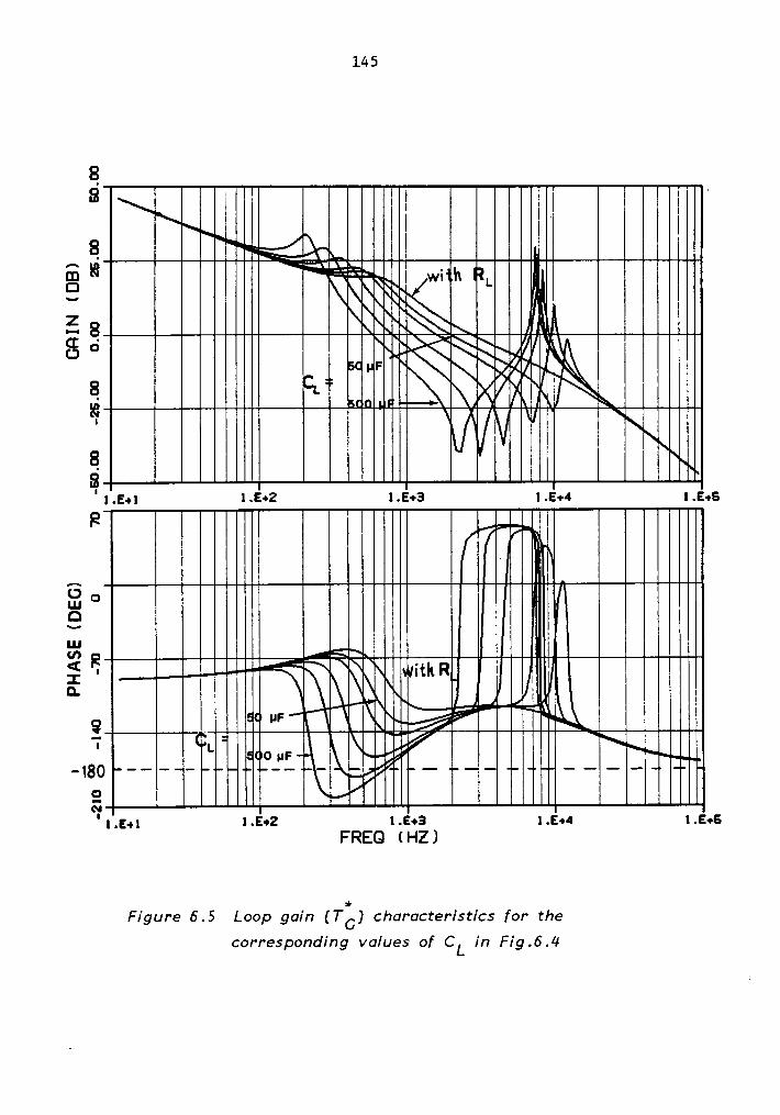
145
ä lll QR E inhlllllällllllllIIIIMIIIIIIIIIIä QII||IIIIII|||. IIIIlllllllsaaggggäwgäigaO • • l).
Ä TI
IIIIIIIIII Ililusäsmwmllllllll„ ‘1 1 ‘8 IIIIIIIIIIIIIIII||IWWIII||IIiI!¤lIl
l „E•l I .E·•2 l .E·•3 I.E+42
l!,!l||'IIIIIIIIlllllllllllümumIIIIIIIIIQ III|III||II||IIII|I|I||||||L“4l||iIIIIII|||E Hg IQ tz.5%_’
‘ ‘ 1 „
lii'|iIi!!Em‘¥!‘ Q ’*""”"l‘¥&IIIIIII|IlIIil'I’i¥ä!*!"iIIIII||I"lII¤iEi"II ..¤«•I u In
1.E+i l•E·•2 FREGI] 1.E•4 I .E•5
Figure 6.5 Loop goin (TZ) chcrrocteristics for thecorresponding vo/ues of CL in Fig.6.4

146
6.3 Source interaction analysis
The source interaction problem of switching regulators was first de-
scribed between an input filter and a regulator [13]. The conclusion can
easily be extended to a general cascade configuration where a preceding
block is viewed as a source impedance to the following block which is a
switching regulator. This interaction analysis can be further extended
to a parallel configuration as in the DET system. Fig.6.6 shows the
system in which switching regulators are sharing a common bus. The source
block represents the solar array, the shunt regulator or the battery
discharger, cable impedances and filters.
As described in the previous section, it is very difficult to analyt-
ically characterize the performance parameters of the regulator including
dynamics of the source. However, using Eq.(6.13), the source interaction
can easily be analyzed similar to the load interaction analysis.
vl 1/Yi 1 lHS I T I
TIT IT T 6vs 1/ i S 1 S. i S ( .13)
In this case, the parameters to be used for the analysis are the input
impedance of the load terminated regulator, Zi, and the source impedance
seen by the regulator, ZS.
In the parallel configuration shown in Fig.6.6, one can. define two
types of interactions: local and global. The local interaction is the
interaction between the source impedance seen by jth regulator,Zsj and
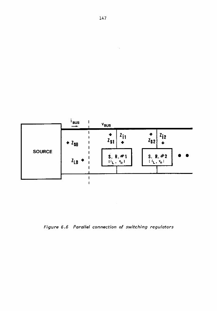
147
F 1Eis Vaus11 Z° ZI2
Ö F {1
SOURCE 1 _1 S. R.#1 S. R.#2 *
ÖZLB
" 1 111. 1.,1 111.11.11
11
Figure 6.6 Parallel connection of switching regu/ators

148
its input impedance, Zij. The global interaction is the interaction be-
tween the source and load impedances seen by the main bus, ZSB and ZLB.
For the source interaction, let us assume that each interacting quantity
(Zsj,Zij,
ZSB,ZLB)
is individually stable, otherwise the subsystem(s)
is(are) already unstable before we consider this interaction problem.
From Eq.(6.13), the system is stable if the polar plot of TS does not
encircle (·l,0) point under the above assumptions. Thus, the condition
|TS| < 1 ensures the above stability criterion. As the number of regu-
lators increases the stability condition moves in the worse direction and
may cause instability of the system because of the negative input
impedance characteristic of the regulators.
Let us consider first the undesired interaction that occurs to a local
jth switching regulator. The source impedance seen by thejth
regulator,
Zsj is the parallel combination of the output impedance of the source
block, ZSB, and the input impedance of all other switching regulators,
ZLj,as described in Eqs.(6.l4) and (6.15).
Ysj = YS + YLj, Zsj = 1 / Ysj (6.14)
nYLj = Z Yik (6.15)
k=1k¢j
To see how other regulators might affect the stability of the jth regu-
lator, let us examine the summing effect of these impedances at low fre-
quencies. Since, at low frequencies, switching regulators have the

149
negative input impedance characteristic, so asZLj,
and the magnitude of
ZLjis supposed to be larger than that of ZSB for a stable design, the
magnitude of the equivalent source impedance seen by thejth
regulator,
|Zsj| decreases as the number of regulators increases. This shows that
a stable system can become unstable if more switching regulators are added
to the main bus. _
An undesired interaction in the global sense can occur when a large
number of converters share the same DC bus which is not a stiff Voltage
source. In this case the magnitude of the load impedance seen by the bus
|ZLB|, which again is negative at low frequency, decreases as the number
of regulators increases as shown in Eq.(6.16).
n
YLB = E Yik , ZLB = l / YLB (6.16)k-1
When the |ZLB| is of the same order of magnitude as the IZSBI an undesired
interaction can occur. In this case the entire bus may oscillate. In
this case, the local interaction may not be directly observable from the
impedance comparison between Zsj andZij,
because Zsj may be already un-
stable due to the global interaction thus it may have RHP poles.
The following cases are generated to illustrate the undesired inter-
action problems described above.
First, a stable system in Fig.6.6 is constructed with only one
switching regulator (S.R.#l - Buck regulator with input filter). Fig.6.7
shows the step load responses where the load power of S.R.#1 steps up from

150
68 IKK I I2 11
.IIII IISI
68 — —— —@1111111O.® O.! 0.75 I.I3 l.5O I.! 2.25 2.53 3.®
3‘so¤.An
8 · KK6'==··¤~T§.II
8 IIIÜII°O.(D O.! O.'E I.I3 I.6O I.! 2.25 2.63 3.CD
raus ms
Figure 6.7 Step tronsient responses for the DET system withone switching regulator (S.R.#1)

151
140 to 200 watts at lms. The system eigenvalues calculated under the
steady-state condition are listed in Table 6.1. The results of both small
signal analysis and time domain simulation show that the system is locally
and globally stable.
Next, a stable switching regulator (S.R.#2 - same structure as that
of S.R.#1 except with different parameter values) is designed. The loop
gain and step load transient responses of S.R.#2 with an ideal source are
shown in Fig.6.8.
Now, the S.R.#2 is connected to the bus, in parallel with S.R.#l, and
the transient analysis of the first case (Fig.6.7a) is repeated. Fig.6.9a
shows that the new system is very oscillatory. The system eigenvalues
as shown in Table 6.2 indicate a lower frequency oscillation of the bus
voltage. Similarly, by comparing the input impedance Zizof S.R.#2 and
the source impedance ZS2 seen by S.R.#2 as shown in Fig.6.9b, the
oscillatory nature of the system can be predicted. Since the two
impedance curves are overlapping in Fig.6.9b, the stability predicted
with the individual regulator in Fig.6.8b is no longer valid because of
a parallel interaction.
To illustrate the undesired interactions in the global sense, let us
consider four well-behaved switching regulators sharing a common bus.
In this case identical switching regulators are used. The system is
stable with a single regulator as Table 6.3a indicates. However, the
system becomes unstable with four regulators in parallel as shown in Table
6.3b. Fig.6.l0 compares the source impedance, ZSB, and the total load
impedance, ZLB, seen by the bus and reveals the undesired interactions.
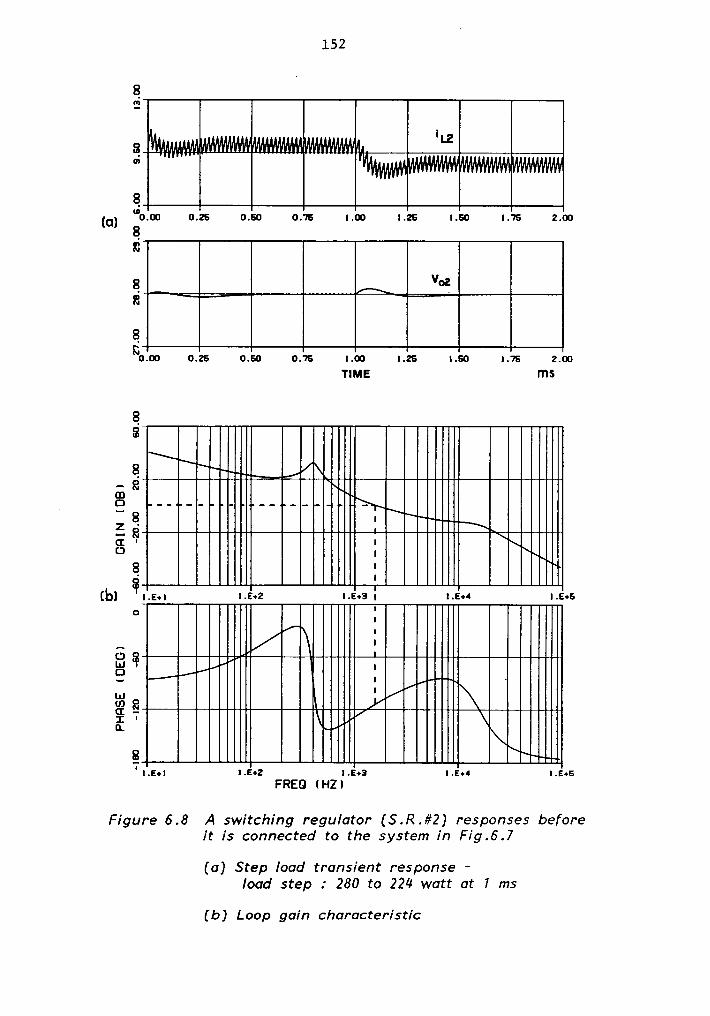
152
6
3 1.11 1 1 111M11111111111111111111111H1111H1H11
”MIEII° WIII“””” """""'"'"'""""6 WWW[G) ;0.lIJ 0.25 0.50 0.75 I.® 1.25 1.50 1.75 2.®
6..8
§0.®0.25 0.50 0.75 1.® I.25 1.50 1.75 2.11)
TIME ITIS
63 uIIIIIIII||IIIIIIIIIIIIIIIIIIIIIII3 Iir’“
IIIIIIIIIIIIII""ul:g Q -.lIIIII). _.3 1 IIIIIIIIIIIIIIII||lI|IIIII|III"'"3 III3II.E•l 1.5+2 I.E+3 | 1.5+4 I.E•5° IIIIIIIII'IIIIIIIIIIIIIIIIIIIIIIIIIä.4.1*3
¤uII|I|lII|I||I|I|I"' "IIIIIIIIä Q 1IV31IIIIIIIIIIII1"1IIIIIIIII|I‘|||||||· 1.5+1 l.E•2 1.5+3 l.5•4 I.E•5
FRE0 (HZ)
Figure 6.8 A switching regulator (S.R.#2) responses beforeit is connected to the system in Fig.6.7
(a) Step load transient response —load step : 280 to 224 watt at 1 ms
(b) Loop gain characteristic

153
6SOLAR
I P ¤6 lM
IDMÄHIIEI;0.® 0.38 0.75 I.I3 h50 hä 2.25 2.53 3.üJ" III V· V I1 HI 4;
m0.® 0.ä 0.75 I.|3 I.50 hä 2.25 2.53 3.l'X)
TIME s ms
“""""'““||I|||IIIIIII|Il|"""|8 IIII IIII-ln., ___'*
W, AnllllllID— IIII IIIIlI||||“·;•"·VIIIIIIIIIIIeg ___. -..¤|II IIII¤..._—. I 'M"*""" 1E
‘66 L
8 IIIIIIIIIIIIIIIII|II|III||IIIIi"“Igs'|,§•| l.E•2 I.E•3 l.E•4 I.E•5
FRE0 lHZ)
Figure 6.9 The system responses after the stable regulator (Fig.6.8)is connected to the stable system (Fig.6.7)
(0) Step transient responses -the same step load for S.R.#7 as in Fig.6.7
(b) The magnitude of the impedances, |z$2| vs lzizl
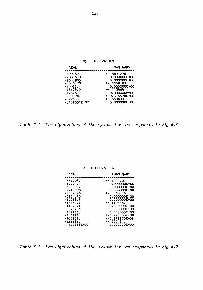
154
15 EIGENVALUES
REAL IMAGINARY
-692.671 +- 489.278-708.619 0.000000E+00-784.905 0.000000E+00-4046.70 +- 4464.83-10033.1 0.000000E+00-13675.9 +- 112464.-14876.1 0.000000E+00-500394. +-0.316578E+08-522133. +- 660439•.102681E+07 0.000000E+00
Table 6.7 The eigenvalues of the system for the responses in Fig.6.7
21 EIGENVALUES
REAL IMAGINARY
-87.937 +- 2514.21-592.471 0.000000E+00-808.237 0.000000E+00-971.228 0.000000E+0O-4047.86 +- 4465.36-6164.15 0.000000E+00-10033.1 0.000000E+00-12460.7 +- 110556.-14876.1 0.000000E+00-22909.5 0.000000E+00-157168. 0.000000E+00-250118. +-0.223800E+08-500391. +-0.316579E+08-522131. +- 660434.—.102681E+07 0.000000E+00
Table 6.2 The eigenvalues of the system for the responses in Fig.6.9

155
88
L L lIIIIlIl§§l||ll··§‘ll' |II'·¤ III||“'ZII"i'"\!!|ll ||IS ci ..«lI.4II“* W"'”|||IIP'‘“I||Znlll
8 lé KIIII IQ u_‘1 und Illlu u|II|II|‘ I8 IIIIII|I|IIIII|IIIII|II|I|IuIIuIII|Q In
' I.E•I I.E•2 I.E•3 I.E•4 I. •S
FREQ (HZ)
Figure 6.70 The mognitucle of the impedances seen by the bus(|z$B| vs lzl-Bl) und seen by $.R.#2 (|z$2| vs |zi2|)
15 EIGENVALUES 33 EIGENVALUES
REAL IMAGINARY REAL IMAGINARY
-670.571 +- 127.77 168.22üU +— 909.¤17-705.9UO 0.000000E+00 -3¤2.1ü9 0.000000E+00-982.262 0.000000E+00 -855.722 0.000000E+00-3Uh7.72 +- 3670.9N -855.722 0.000000E+00-7H11.92 +- 12070.5 -855.722 0.000000E+00-11¤902. 0.000000E+00 -1218.23 0.000000E+00-233717. 0.000000E+00 -3U63.95 +- 3681.63-2713¤8. +- 18ü089. -¤083.17 +- 7396.58-907316. 0.000000E+00 -ü083.17 +- 7396.58-.2¤9996E+08 +-0.9997U5E+09 -U083.17 +- 7396.58-1793u.Ü +- 16539.5
-11N106. 0.000000E+00-11U106. 0.000000E+00
. -11¤106. 0.000000E+00-11832U. 0.000000E+00-233717. 0.000000E+00-259219. +- 179965.-907316. 0.000000E+00-.2U9996E+08 +-0.999695E+09-.2¤9996E+08 +-o.999696s+69-.2¤9996E+08 +-0.999695E+09-.2¤9996E+08 +-0.999895E+U9
Table 6.3 Eigenvo/ues of the system
(0) with single switching regu/otor(b) with four switching regulators

156
However, by comparing the source impedance, Zsl, and the input impedance,
Zil, seen by the individual regulators, the presence of the undesired
interaction to an individual regulator is not obvious. From Eq.(6.l3),
the sufficient condition for stability is [Zi] > IZSI under the assumption
that both Zi and ZS are stable. ln this case, the source impedance, ZS1,
seen by S.R.#1 is unstable (has RHP poles) because the undesired inter-
action already occured between ZSB and ZLI. Thus, even though |Zil| >
|ZSj| for all frequencies as shown in Fig.6.10, the system is unstable.
This reveals that the analysis must be done at both the local regulator
level and the system level.
6.4 Conclusions
The subsystem interaction criteria are investigated at component,
subsystem, and system levels by comparing the impedances at an interacting
point.
Both the load and the source interaction problems are illustrated using
the switching regulator examples. The performance of the regulator de-
pends upon the dynamic characteristics of the payload. As demonstrated
in this chapter, a single filter capacitor between the regulator and
equipment (load) can cause system instability due to the load interaction.
The load interactions can be investigated using the output impedance of
the unterminated twO·pOrt subsystem (component), g22,and its load
impedance, ZL.

157
For a spacecraft power system that uses many switching regulators in
parallel on the bus, such as the DET system, the interaction problem
should be examined both at the local regulator level and the system level.
Also, the analysis shows that as the number of regulators increases, the l
margin of stability of the system tends to diminish due to the parallel
interactions.

Chapter 7 ·
EMPIRICAL DATA MODELING AND ANALYSIS
7.1 Introduction
As discussed in Chapter 2, defining mathematical models through ex-
perimental testing of an actual system (or scaled model) is, generally,
least intensive in modeling effort and the empirical data model is accu-
rate in predicting the overall system behavior. In general, experimental
data serves two major functions: model Verification and model develop-
ment. If a theoretical model has been developed, at some point its va-
lidity must be checked with actual experimental test data to have a high
level of confidence in its predictive capabilities. Also, some systems
defy refined theoretical treatment due to the lack of an assessment of
certain parameter values, thus, experimentation is the only effective
means of obtaining models with acceptable accuracy. In this chapter,
model development based on empirical data is discussed and extended for
the reduced order model realizations of a complex system.
In Section 7.2, model development from the frequency response data and
its applications are described. Algorithms for identification of model
parameters identification are reviewed in Section 7.3. In Section 7.4,
model development and analysis using the DET system are presented. Con-
clusions are presented in Section 7.5.
“158

159
7.2 Model development from frequency response data
Typical methods for linear system identification using empirical data
are based on frequency, step, and impulse responses. Most of these
methods apply to a linear process, but they may also be applicable to the
linearized form of nonlinear systems if the input disturbance levels are
kept low. Among these, frequency-response identification provides the
most accurate model realization for the system stability. Since gener-
ation of the sinusoidal input signal and measurement of its responses,
i.e. audio susceptibility, feedback loop gain, impedances, etc., are not
foreign to power system design engineers, the frequency response tech-
nique is more attractive than others.
Using an automatic network analyzer that includes a multi-channel
bandpass tracking filter for gain and phase measurements and a bui1t—in
sinusoidal function generator synchronized with the tracking filter, ac-
curate frequency response data of the system can easily be obtained.
Where a model of an existing subsystem is to be constructed, empirical
data can be obtained that characterize the input-output properties. Based
on the set of empirical data a mathematical relation can be established
that reproduces the same input-output behavior as that of the actual
subsystem without regard to the physical structure of the subsystem.
The empirical data modeling technique can be used for the following
applications.

_ 160
Model development from experimental data:
For certain components or subsystems, such as a complex payload, cable,
etc., it is often quite difficult to develop an analytical model. Under
such circumstance the component or subsystem is viewed as a black box.
The port characteristics of the black box can be experimentally measured
by exciting an appropriate terminal with a sinusoidal source. From the
experimental data, in the form of the frequency response, an analytical
transfer function model can be developed using the complex curve fitting
technique. The required transfer function model to represent properly
the input-output characteristics of a black box will be described in the
following section.
Reduced order model realization:
The model development from frequency data using the complex curve
fitting technique can also be applied to reduce the order of complexity
of the system. The technique is particularly powerful for large scale
system modeling and analysis. For a large scale power system, computer
· simulation of an entire system can be very time consuming and memory ca-
pacity often exceeded. It is desirable that the entire system be broken
into smaller subsystems so that an available computer system and software
can be adapted. Each subsystem can then be simulated by the computer,
or experimentally measured to obtained the frequency response data. From
either the analytical or the empirical data a reduced order model can be
realized using the complex curve fitting technique. As long as a reduced
order transfer function model fits the original data reasonably well the

161
dynamic performances of the reduced order subsystem should match well with
that of the original system. This technique allows the overall system
to be realized with a reduced order model. More importantly, it aids in
the trouble-shooting and design of a component or a subsystem in a large
scale system. Using this technique, attention can be focused on the
"troubled" equipment or subsystem in greater detail while treating the
rest of the system with a reduced order model to take into account any
possible interactions.
7.3 Review of the existing complex curve fitting algorithms
As described in the previous section, the purpose of the frequency
response approach is to develop a transfer function model from the two
sets of data, the amplitude ratio and the phase difference of the input
and output. While methods for fitting curves to empirical data are a well
known part of classical mathematics, the need to fit two curves (amplitude
and phase) simultaneously over a wide range of frequencies requires a
somewhat different treatment from the classical approaches. Several
methods documented in the literatures are reviewed in this section.
One of the earliest methods by Levy [14] that dealt with the funda-
mentals of complex curve fitting is briefly reviewed here. This method
requires that the measured frequency response be given in terms of its
real and imaginary parts:
Qo . . .(aw) = F(J<~¤) E R(w) + 1 1(w) (7-1)

162
Let the fitted analytical model be
I — AO + A1(jw) + A2(jw)’ + ...
B0 + Bl(jw) + B2(jw)2 + ...
. a + jwß N(w)E --————- E -————- (7.2)
o + jwt D(w)
The error of fitting, s(w) is then
N(w)=(w) = F(jw) · G(jw) = F(jw) - ——— (7-3)
D(w)
To minimize the square of the error, s(w) (conventional least-square
method), a set of simultaneous nonlinear equations results, whose sol-
ution is difficult. Instead, a new error function is defined by multi-
plying D(w) into Eq.(7.3)
s' = D(w) s(w) = D(w)F(w) - N(w) E a(w) + j b(w) (7.4)
Then the cost function for m+l points of frequency data is defined as
mJ = E [
a’(wk)+
b“(wk)] (7.5)
k=0

163
To minimize the cost function J with respect to the coefficient vector,_ T
p — [AO ... Am B0 ... Bm] , set
GJ——- = 0 (7.6)ap
Eq.(7.6) leads to the linear algebraic equation
Xp=Q ' (7-7)
whereX = nxn coefficient matrix, n = m+1
Q = nxl constant vector
Finally, the solution for the model coefficient is
_ -1p — X Q (7.8)
This algorithm is simple allowing a standard library function for the
matrix inversion routine to be directly adapted. However, this technique
has some serious deficiencies. If the transfer function has to be de-
termined for frequencies extending several decades, the matrix X has a
"rank deficiency". In other words, the elements of the matrix X are such
that lower frequency values have very little influence. Thus, large er-
rors can be introduced at low frequencies. If the poles in G(jw) vary
widely throughout the experimental points a good fitted model cannot be
obtained.

164
To overcome the deficiencies, an iterative procedure is introduced in
[15] that eliminates the weighting problem in the above method. This
method improves the above algorithm by modifying Eq.(7.4) such that
‘(“k) D(“k)L F(j“k) D(wk)L N(wk)L (7.9)g"(w):l..:;..—l.:k
D(wk)L-1 D(wk)L-1 D(wk)L-1
where the subscript L corresponds to the iteration number. As D(w) is
not known initially, it is assumed to be 1. The coefficients are obtained
by minimizing the sum of [sk]! at all the data points. This algorithm
fits the data much better over a wider frequency range than the algorithm
in [14] and the iterations tend to converge rapidly.
A more recent effort in [16] uses a conjugate gradient search technique
[17] to minimize the nonlinear cost function
ä_
2
J = f [ F(jw) - A(w) eJ8(w)[ dw
0
lll . 1=
. _ J6(w ) _
E[ F(Jwk) A(wk) e k [
(wk+1wk_l) (7.10)
k—0
In this algorithm, the model is allowed to be characterized by a gain,
real poles and zeros, and complex poles and zeros with the damping ratios.
It also allows for dead time in the model, which is not possible in the
previous methods [14] and [15]. A FORTRAN program listed in [16] is

165
implemented in the host software for this study.
Curve fitting results, in general, are quite satisfactory as will be
seen in the following section. However, the results (or the number of
iterations required for the error to be in the specified bound) depend
on the initial guess of the coefficients which is especially critical when
one uses a wrong sign for the initial guess.
7.4 Empirical data modeling and analysis of power systems
As mentioned in Section 7.2, the required model for a subsystem depends
on the modeling objectives. Whether a subsystem is considered as a black
box or is realized as a reduced order model, the subsystem to be modeled
can be defined in the system as either an one-port or two-port model.
0ne—port modeling:
To analyze the behavior of a component or subsystem whose load or
source characteristic is unknown or is to be realized as a reduced order
model, the load or source subsystem can be defined as an one-port network.
In this case, only one transfer function model (impedance) is needed to
represent the subsystem. From the frequency response data of the
impedance obtained from either experimental measurement or computer sim-
ulation of the circuit model, an analytical model can be developed using
the complex curve fitting technique. The system performance parameters
such as stability, audiosusceptibility and impedances can be analyzed
using the curve fitted model. Time histories including step transient

166
responses of the system can be simulated. The step transient analysis,
however, is valid for a small disturbance level. The curve fitted ana-
lytical model also allows one to analyze the source and load interaction
problems.
To illustrate one—port modeling, the following cases are considered
using the DET system shown in Fig.4.l.
First, assume that the switching regulator subsystem, S.R.#l, is a
black box that can be viewed as one of the loads on the main bus line.
The black box can then be characterized by its input impedance, Zil,which
can easily be measured experimentally. An analytical transfer function
model is then developed that represents S.R.#l as shown in Fig.7.l. Curve
fitted results of Zil data using the 3rd order model is shown in Fig.7.2.
Using this model, the behavior of the system (i.e., the bus Voltage) due
to the disturbances at the source or at the other load (S.R.#2) can be
examined. To show the results of one of the aforementioned analyses,
Fig.7.5 and 7.6 compare the transfer functions from the solar array output
Voltage, VS, to the bus voltage, VB, and to the output Voltage of S.R.#2,
voz, between the system with the actual circuit model and that with the
curve fitted model. As the curve fitted result in Fig.7.2 predicted, the
system responses are almost identical between the two system.
Secondly, model the subsystem of the total load on the bus line from
empirical data as shown in Fig.7.3. The frequency response data of the
load impedance seen by the bus,ZLB,
is obtained either by experimental
measurement or by computer simulation to realize a reduced order model.
The actual circuit model which is a 16th order model and curve fitted

167
results of ZLB data using the 4th order model is shown in Fig.7.4. Using
this model, the behavior of the bus Voltage can be examined as in the
previous case. Stability of the solar array equilibrium point can be
analyzed in detail. Also, the performance parameters such as the loop
gain characteristic of the shunt regulator can be analytically deter-
mined. Fig.7.5 also includes the frequency response from the solar array
output Voltage, VS, to the bus Voltage, VB, for this case. Again the.
result matches extremely well with the original system.•-
Two-port modeling:
As mentioned in Chapter 3, modeling of the distribution cable is Very
difficult. To characterize such a component it is necessary to view it
as an unterminated two-port network and model its terminal character-
istics. Thus, in this case, four sets of frequency response data are
needed to identify the four elements in the G-matrix. As described in
Fig.2.2 of Chapter 2, port-1 is excited by a Voltage source forgll
and
gzl,and port-2 by a current source for
glzand gzz. Since the hybrid
g-parameters can be converted to the open circuit z-parameters or short
circuit y-parameters, as shown in Eq.(7.l1), appropriate experimental
measurements can easily be obtained.
'1 212 'AYzlly22G= = (7.11)
E li hi Lzll zll y22 y22

168
Vs VB
CABLE /
FILTERS
SHUNT
REGULATOR
Figure 7.1 DET system with the empirical data curve fittedmodel for $.R.#1 1
IIIIIIIIIIIIII IIIIIIIIIIIIIIIIIC IIII I2 ,4 IIIIIIIIIIIIIII IIIIIII I IIIU)(II
“’ I IIIIIII III |III'E"'IIIIIIIIIII III IIl!II.....•¤II| IIIIIIIIIIIIIIIIIIIII II
I l.E•l _IY.E•2 I.E•3 ~_ M l.E•4 I.E•5 l.E•6
IIIIII IIIIIIIII IIIIIIIIIIIII II"II|II? Al
é. IIIIIII|Ill;„. .«IIII""I "'I|||IIIIIIIIIIII|| 'II III„.„ 4; IQ [
EE Ij I-}; A4
8 IIIIIIIIIIIIIIIIIIIIIIIIIIIIIIIIIIIIIIIII I18 ;.IIIl.E•l I.E•2 l.E•3 I.E•4 I.E•5 l.E•8
FREI) (HZ)
Figure 7.2 Curve fitting for zi,
• • • • : empirical data-——— : curve fitted cma/yticol model

169
CABLE / FILTER
FILTERSZLB
A I“"'°suuur nssuuron (s.n.#¤, s. nf:)
Figure 7.3 DET system with the reduced order model(1LB for $.R.#1 and S.R.#2)
8“IIII IIIIIIIIIIIII I"I?’ IIIIIII II 'E IIII—KIlIu•.. ‘ A r A
ä I3 I AIIIIIII IIIIIIII III II IIIIIII IIIIIIIIIIII IIIII'I II IIIIIIIIIIIIIIIIIIII3 III I...•IIIIIIIIIIIIIII IIIIIIIIIIIIIIIII II I
IIIIIIIIIIIIIIIIIIII II2 „, I .N T | ITU') Y3 I II2 2 J’
l|IIII""iI|II IIIIIIIIIIIIIIIIII IIII II
LE,} l.E•2 l.E•3 l.E•4 l.E•S |.E•6FREI] (HZ)
'Figure 7.4 Curve fitting for 2LB• • • • : empirical data of the 76th order circuit model
—— : curve fitted 4th order analytical model

170
IIIII|IIWIIIIIIIIIIIIIIIIIIII IIl'iI|IIII“"""'lIIIIIIIIIII I
E“ I IIIIIII|III|||IIIIII"'I|I IIII IIIg R hh. ‘.IIIIIIIIIIIIIIIIIIIIIIIIIIILIIIIIIIIl.E•l |.E•Z l.E•3 I.E•l l.E•5
IIIIIIIIIII HIIIII IIIIIII III I Ié 8*I IIIIII II*""""III|IIIIIII|II““m|L"|II|IIIIIIIIII.II||II IIIIIIIIIIIIh•„....-.......„
Il.E•l |„E•Z ° I.E•3 l.E•l l.E•S
FREG (HZ)
Figure 7.5 Frequency response from vs to VB
A : The exact system modelB : with empirical data model for ZH in Fig.7.1C : with reduced order model for ZLB in Fig.7.3D : with two·port fltted model for the cable in Fig.7.7

l7l
8 lllllm NX""“
II NIIIIIIIIIIIIII III___ " NC) IIIIIIIINMII N INNIIIIIIIIIIII II
IIIIIIIIIW NI|N'IIIII||||IIII||äg n. N;_( IIIIIIIIIIIINIIIIIII"'"““""g Iuuu-IIIIIIINI|.E•I I.E•2 A l.E•3 I.E•4 l.E•5
8
I||!!IIIIII!!lIl...„ü.... .|IlI|II|I|H}| IIIn|III|||| IIIINIIIHIIIIII IIIE N IIIIII ||IIIIIII||II'|I||||I IIIgs M.,IIIIII I|II||II|IIIIIII|N"I II III5 II;
Il.E•| l„E•2 l.E•3 l.E~4 |.E•5
_ FREG (HZ)
Figure 7.6 Frequency response from vs to voz
A : The exact system modelB : with empirical data model for zi, in Fig.7.7D : with two—port fitted model for the cable in Fig.7.7

172
SHUNT FILTERREG.
gl] gi) _
¢ s. n. 1 IoFILTER gz]
S.R. Ü
Zi Zo
Figure 7.7 Empirical data mode/ing of two—port component (Cable)

173
The G-matrix model fully characterizes the two-port black box. The model
is connected to the system according to the interconnection law which
results in a doubly terminated two-port system.
As shown in Fig.7.7, the two—port cable/filter model in the DET system
is modeled using empirical data. The frequency responses in Figs.7.S and
7.6 using these fitted models again match very well with the exact model.
7.5 Conclusions
In this chapter, empirical data modeling and analysis of power systems
is discussed. The analytical transfer function model of a one-port and
two-port black box can be developed based on the measured frequency re-
sponse of port characteristics.
A reduced order modeling technique is also implemented using the com-
plex curve fitting method. This technique allows the elimination of
non-dominating poles and zeros as well as poles and zeros in close prox-
imity, which can be ignored for all practical purposes. The reduced order
model greatly facilitates analysis and trouble—shooting of complex
spacecraft power system and with much improved computational efficiency.

Chapter 8
CONCLUSONS
The principal objective of this dissertation is the development of a
comprehensive large scale power system modeling that facilitates the de-
sign and analysis of present and future spacecraft power systems. Meth-
odologies of model building and analysis of large scale power system are
presented.
The principal goal is accomplished by utilizing the modular concept
such that the total system is configured by interconnecting individual
component modules. The hybrid g-parameter two-port subsystem coupling
method is employed as the standard interconnection law. This providesl
bi-directional information flow among components so that the maximum
flexibility can be achieved in system model building. The flexibility
in model building gives more than convenience but the success of the
system level modeling depends largely on it due to the difficulties in-
volved in large scale system modeling as stated in Chapter 1. The modular
approach also allows the system performance parameters to be expressed
as both analytically and empirically measurable quantities. Thus, the
model can be verified at various component levels. Also, since the system
performance parameters such as stability, audiosusceptibility, impedance
characteristics, etc. are derived with a focus on either local or global
behavior, the model allows one to predict and trouble-shoot the undesired
interactions that often occur among various subsystems.
174

175
The success of the system level model building reduces the uncertain-
ties in the model to the component level which implies the accuracy of
the system model depends now on that of component models. As stated in
Chapter 1, behaviors of individual components of spacecraft power system
are mostly well understood and new and more powerful techniques for com-
ponent level modeling are currently under development. In this study,
existing component modeling techniques are adapted to develop untermi-
nated component models (two·input, two—output). Each model consists of
large signal time-domain model and small signal model. The large signal
model simulates the actual behavior of the system including various non-
linearities in the practical circuit. The small signal model character-
izes dynamics of the system about a steady state operating condition.
The integration of the component models is done by the host software
system, EASY5, which was identified from the preliminary study of appli-
cable existing software systems, as the most suitable general purpose
program. It provides maximum flexibility in component model building such
that each component can be modeled with state differential or difference
equations, transfer functions, empirical data and combination of these.
The comprehensive analysis of a spacecraft power system, the secondary
goal of the study, is performed using the Direct Energy Transfer (DET)
power system as an example. Also, the large signal behavior of the gen-
eral solar array spacecraft power system is analyzed.
The nonlinear solar array output characteristic coupled with a con-
stant power load is shown to result in multiple equilibrium points. The
state plane analysis shows that the equilibrium points in the region where

· 176
the solar array behaves as a constant current source are unstable. There
exists a separatrix in this region which separates the state plane tra-
jectories into two distinct patterns that ultimately lead to two quite
discernible operating points. However, only one, corresponding to the
solar array constant Voltage source region, is the desirable system op-
erating point. Thus, the system's initial start·up condition must be set
in such a way that it leads to the desired operating point.
The behavior of the operating point near the solar array maximum power
point is analyzed. Regarding stability and transient response, system
operation in this region is less commendable than in the region where the
solar array behaves as a stiffer Voltage source. One way of improving
dynamics of a system that utilizes the solar array maximum available power
is to dissipate some power in a shunt circuit. This makes the source
characteristic a stiff Voltage source.
Since the battery discharger in the DET system operates over a range
from a no-load condition through the discontinuous conduction mode (DCM),
to the continuous conduction mode (CCM), the feedback compensator of the
battery discharger regulator must be designed carefully to ensure the
stability for all conditions. A proportional gain control is most ap-
propriate for a converter operating in DCM to speed up the system re-
sponse. In CCM, a phase lead type compensator is required to compensate
the excessive phase lag from the complex pole. Thus, integrator is not
suitable for a compensator in the battery discharger regulator because
of the power stage open loop pole near the origin.

· 177
One of the major difficulties in large scale power system analysis is
the subsystem interaction problem. The unterminated two-port component
modeling allows one to investigate the interactions at the component,
subsystem and system level viewed from either the source or the load.
For a spacecraft power system that uses many switching regulators
lconnected in parallel on a common bus, such as in the DET system, inter-
actions should be examined both at the local level and the system level.
Analysis shows that as the number of regulators increases, the margin of
stability of the system tends to diminish due to the parallel inter-
actions.
As stated in Chapter 7, due to the lack of an assessment of certain
parameter values in some spacecraft component models, experimentation is .l
the only effective means of obtaining models with acceptable accuracy.
Employing the complex curve fitting technique, the analytical transfer
function model of a one-port and two-port black box is developed based
on the measured frequency response of the port characteristics. If the
fitted model reasonably matches (over the frequency range of interest)
_ the frequency response of the black box, the two subsystems are expected
to be dynamically equivalent. This is verified by performing a system
level analysis using both the fitted model and the actual model for a
subsystem .
A reduced order modeling technique is also implemented using the com-
plex curve fitting method. This technique enables one to eliminate non-
dominating poles and zeros as well as poles and zeros in close proximity
which can be ignored for all practical purposes. The reduced order model

178
greatly facilitates the analysis and trouble-shooting of a complex
spacecraft power system with much improved computational efficiency.

179
REFERENCES
1. J. Cassineli, et al., "Analytical Modeling of Spacecraft Power Sys-tem," Final Report to NASA GSFC, 1982, TRW, Redondo Beach, CA
2. D. L. Sommer, I. S. Mehdi, "High Voltage DC Electrical System Sta-bility Ana1ysis," Final Report to Naval Air Development Center, Oct.1979, Boeing Military Airplane Company, Seattle, WA
3. R. D. Middlebrook, S. Cuk, "A Generalized Unified Approach to ModelingSwitching Converter Power Stages," IEEE PESC 1976
4. D. J. Short, "An Improved Switching Regulator Power Stage Model usingDiscrete-Average Techniques," Ph.D. Dissertation, 1982, VPI&SU
5. D. J. Packard, "Discrete Modeling and Analysis of Switching Regula-tors," Ph.D Theis, CIT Pasadena Calif., May 1976
6. B. H. Cho, F. C. Lee, "Feasibility Study of Analytical Modeling ofSpacecraft Power System," Final Report to Naval Research Lab., Aug.1983, VPI&SU
7. J. M. Voss, J. G. Gray, "A Regulated Solar Array Model - A Tool ForPower System Analysis," IEEE PCSC 1970 pp.l2-17
8. A. Capel, et al., "Power System Simulation of Low Orbit Spacecraft:The EBLOS Computer Program," IEEE PESC 1982, pp.272-285
9. R. D. Middlebrook, S. G. Kimble, "Design of the HEAO Main Bus ShuntRegulator," IEEE Trans. AES, March 1976
10. W. Burns,III, et al., "A Digital Simulation and Study of Direct EnergyTransfer Power Conditioning System," IEEE PESC, 1975 pp.l38—l49
ll. D. K. Decker, "Methods for Utilizing Maximum Power from a Solar Ar- ·ray," JPL Quarterly Technical Review, April 1972, pp.37-47
12. E. N. Costogue, S. Lindena, "Comparison of Candidate Solar ArrayMaximu Power Utilization Approaches," IECEC 1976, pp.1449-1456
13. R. D. Middlebrook, "Input Filter Considerations in Design and appli-cation of Switching Regulator," IEEE IAS 1976
14. E. C. Levy, "Complex-Curve Fitting," IRE Trans. Auto. Cont., May 1959
15. C. Sanathanan, J. Koerner, "Transfer Function Synthesis as a Ratioof Two Polynomials," IEEE Tran. on Auto. Cont., Jan. 1963, pp.56-58

180
16. R. Seidal, "Transfer Function Parameter Estimation from FrequencyResponse Data," NASA tm x3286, 1975
17. R. Fletcher, C. M. Reeves, "Function Minimization by Conjugate Gra-dients," Computer J., vol. 7, No. 2, July 1964, pp.149—154
18. D. Zerbel, D. Decker, "AC impedance of Silicon Solar Cells," IECEC,1970
19. P. Chen, et al., "Experimental Determination of Series Resistance ofp-n Junction Diodes in Solar Cells," IEEE Tran. on Elec. Devices,vol.ED—25, march 1978, pp.386·388
l
20. C. Fang, J. Hanser, "Comparison of Theoretical and Experimental SolarCell Performance," IECEC 1978
21. P. Chetty, et al., "Microprocessor Controlled Digital Shunt Regula-tor," IEEE Tran. on AES, March 1980, pp.l91-200
22. F. C. Lee, et al., "Generalized computer Aided Discrete Time DomainModeling Analysis of DC-DC Converters," IEEE PESC 1977
23. F. C. Lee, et al., "Modeling of Switching Regulator Power Stage withor without Zero-Inductor-Current Dwell Time," IEEE IECI Trans. Aug.1979
n
24. W. M. Rintala, et al., "Intelsat V Power Control Electronics System,"IECEC 1979, pp.1349—1349
25. E. Doebelin, System Modeling and Response, John Wiley & Sons, 1980

Copyright © 2022 FDOKUMEN