Tunable Electroluminescence in Planar Graphene/SiO 2 Memristors
Upload
independentCategory
view
4download
0
Microstructure and Optical Properties of Oxygen-Annealed c‑Si/a-SiO2 Core−Shell Silicon NanowiresBhabani S. Swain,† Bibhu P. Swain,*,‡ Sung S. Lee,† and Nong M. Hwang†
†Department of Materials Science and Engineering, National Research Laboratory of Charged Nanoparticles, Seoul NationalUniversity, Seoul, Republic of Korea‡Research Center for Photovoltaics, National Institute of Advanced Industrial Science and Technology, Tsukuba, Japan
ABSTRACT: Core−shell silicon nanowires (Si-NWs) weresynthesized by chemical vapor deposition (CVD) using SiH4and H2 as precursors. The electron microscopy results revealedthat the core shell Si-NW consists of core Si surrounded bythick amorphous silicon oxide (a-SiOx). The diameter of coreSi in a core−shell Si-NW was controlled by varying the oxygenflow rate and annealing time. The morphology of core shell Si-NWs is changed to silicon nanocoils (Si-NCs)/siliconnanonoodles (Si-NNs) after being annealed in oxygenatmosphere. The Fourier transform infrared spectroscopy(FTIR) study confirmed the changes of Si−Si and Si−O−Sivibration band and the intensity of Si−O−Si vibration modeincreases with decreasing diameter of Si-NWs. The opticalproperties of core−shell Si-NWs are improved after being annealed in oxygen atmosphere. The chemical bonding andphotoluminescence properties of oxygen annealed Si-NWs are also discussed in this article.
1. INTRODUCTION
Core−shell nanostructures such as nanoparticles/nanowireshave a great potential in a wide range of device applicationssuch as solar cell, light emitting diode, drug delivery, anodematerials for Li ion battery, etc.1−6 Specially, silicon nanowire(Si-NW) based optoelectronic devices have attracted attentionbecause of their potential application in various devices.7,8 Incore−shell Si-NWs, a-SiOx shell provides a physical barrier tothe optically active core silicon (Si) and determines the overalloptoelectronic properties. The outer shell provides efficientpassivation of the surface trap states, which give rise to astrongly enhanced fluorescence quantum yield. Moreover, thesurface-charge density in Si-NWs could be decreased by a high-quality thermal oxide.9 Hence, a great effort must be made tomodify the thickness of core Si as well as the interface geometryduring the synthesis of Si-NWs to improve the opticalproperties. One of many methods to control the diameter ofcore Si would be to anneal Si-NWs in controlled atmosphere.Sutardja et al. described various modeling approaches of Si
oxidation process.10 Xie et al. also investigated the directionaloxidation of Si-NWs from Au−Si cap to bottom.11 Althoughseveral reports have studied the oxidation of Si-NWs,12−17 theunusual shape transformation of core−shell Si-NWs duringoxygen annealing has not been reported elsewhere.In this article, the peculiar microstructural change of Si-NWs
during annealing in oxygen atmosphere is discussed on thebasis of experimental facts. Moreover, the effects of oxygenannealing on vibrational and optical properties of core shell Si-NWs are also discussed.
2. EXPERIMENTAL SECTION
2.1. Synthesis of Si-NWs. In our experiment, Au-catalyzedSi-NWs were deposited on boron doped Si (100) wafer(resistivity, 1−10 ohm cm) by atmospheric pressure chemicalvapor deposition (CVD), reported elsewhere.18−23 The Si-NWswere deposited with typical process parameters (SiH4, 4standard cubic centimeter per minute (sccm); H2, 5 sccm;N2, 1000 sccm). The furnace and substrate temperatures weremaintained at 1100 and 800 °C, respectively. The Si-NWs wereannealed in varying oxygen and nitrogen flow rate. Theannealing temperature was fixed at 900 °C. During annealing,the oxygen and nitrogen flow rates were varied, but the totalflow rate was fixed at 1000 sccm.
2.2. Characterization. The microstructural evolution ofcore shell Si-NWs was analyzed by field emission scanningelectron microscopy (FE-SEM, Model No. JEOL-JSM 6770).The crystallinity and thickness of core Si were analyzed by high-resolution transmission electron microscopy (TEM, JEOL-JEM-3000F). The TEM samples were prepared by wrapping Si-NWs from the wafer and dissolved in a beaker containingethanol and placed in an ultrasonic bath for 2 min to avoidagglomeration. Two drops of solution were put on the carboncoated copper grid (400 mesh size). Then, the TEMobservation was carried out with a voltage of 300 KV. Thevibrational characteristics of Si-NWs were characterized by
Received: July 9, 2012Revised: September 5, 2012Published: October 9, 2012
Article
pubs.acs.org/JPCC
© 2012 American Chemical Society 22036 dx.doi.org/10.1021/jp3067876 | J. Phys. Chem. C 2012, 116, 22036−22042
Fourier transform infrared spectroscopy (FTIR) by Nicola2000 spectrometer. Before observation, the FTIR of bare Siwafer was taken and subtracted from the original data of as-synthesized Si-NWs to get the data of annealed Si-NWs. Roomtemperature photoluminescence (PL) spectra of Si-NWs wereanalyzed by a PL spectrometer using the 514.5 nm line of Ar-ion laser. The optical properties of Si-NWs were analyzed byUV−vis-NIR spectroscopy (Hitachi, U-4000). After back-ground correction, the reflection spectra were collected forcore−shell Si-NWs.
3. RESULTS
3.1. Microstructure Overview. The microstructure of as-synthesized Si-NWs has been reported in our previousreport.22,23 The as-synthesized Si-NWs were straight with asmooth surface and extended up to several micrometers. Thediameter of Si-NWs was in the range of 60−80 nm.23 Thecrystallinity of Si-NWs was confirmed by TEM and Ramanspectroscopy.20 The Raman peak of core shell Si-NWs appearsat 518 cm−1 and confirms that the core Si consists of singlecrystalline Si.22 The thicknesses of core Si and outer SiO2 layerare 22 and 24 nm, respectively.23
Although our previous study fabricates core−shell Si-NWs ina chemical vapor deposition reactor, the fabrication of Si-NWsof a few nanometer in thickness (below 10 nm) is a difficulttask. The present study attempts to fabricate Si-NWs of a fewnanometer in diameter by annealing in oxidized atmosphere.Figure 1 shows the microstructure evolution of oxygen
annealed Si-NWs at different oxygen flow rate. Figure 1a,b
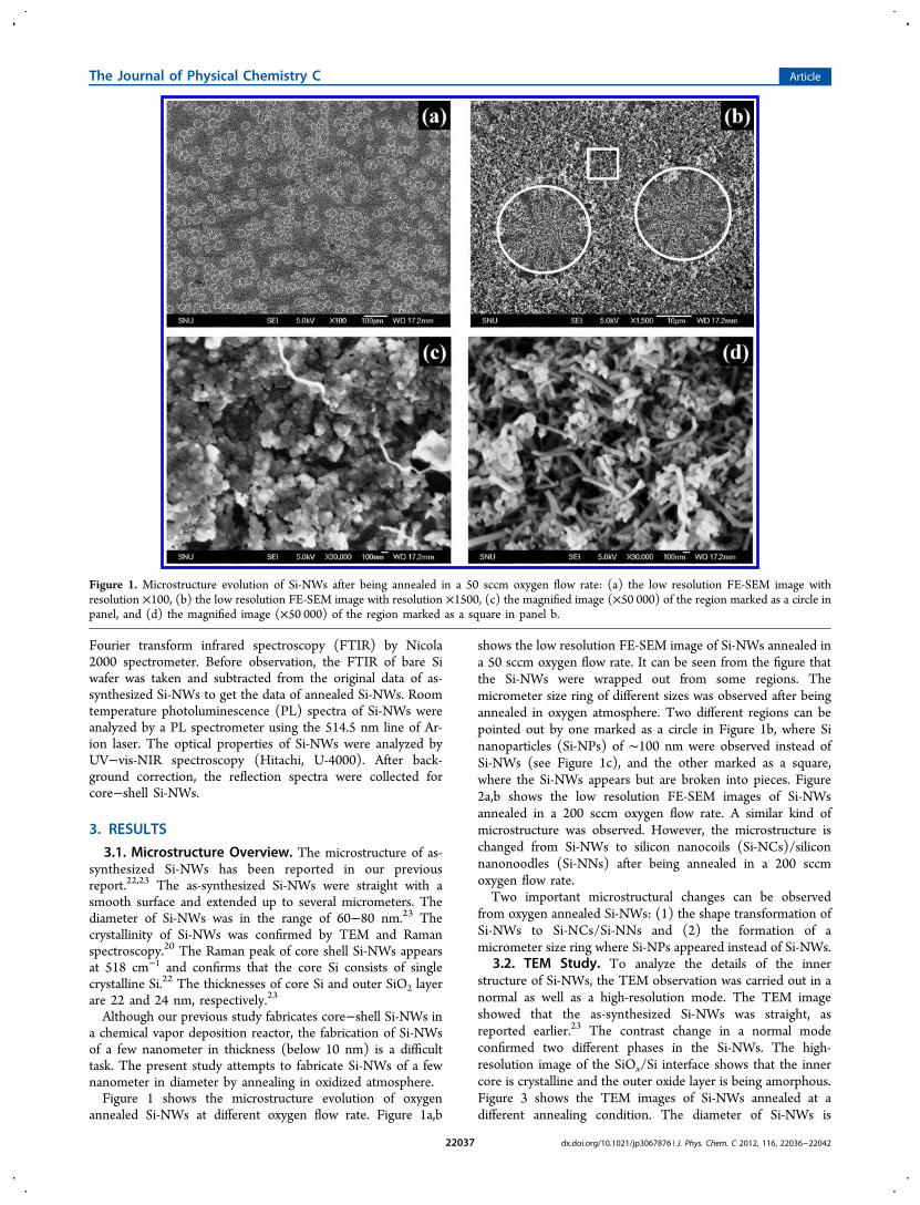
shows the low resolution FE-SEM image of Si-NWs annealed ina 50 sccm oxygen flow rate. It can be seen from the figure thatthe Si-NWs were wrapped out from some regions. Themicrometer size ring of different sizes was observed after beingannealed in oxygen atmosphere. Two different regions can bepointed out by one marked as a circle in Figure 1b, where Sinanoparticles (Si-NPs) of ∼100 nm were observed instead ofSi-NWs (see Figure 1c), and the other marked as a square,where the Si-NWs appears but are broken into pieces. Figure2a,b shows the low resolution FE-SEM images of Si-NWsannealed in a 200 sccm oxygen flow rate. A similar kind ofmicrostructure was observed. However, the microstructure ischanged from Si-NWs to silicon nanocoils (Si-NCs)/siliconnanonoodles (Si-NNs) after being annealed in a 200 sccmoxygen flow rate.Two important microstructural changes can be observed
from oxygen annealed Si-NWs: (1) the shape transformation ofSi-NWs to Si-NCs/Si-NNs and (2) the formation of amicrometer size ring where Si-NPs appeared instead of Si-NWs.
3.2. TEM Study. To analyze the details of the innerstructure of Si-NWs, the TEM observation was carried out in anormal as well as a high-resolution mode. The TEM imageshowed that the as-synthesized Si-NWs was straight, asreported earlier.23 The contrast change in a normal modeconfirmed two different phases in the Si-NWs. The high-resolution image of the SiOx/Si interface shows that the innercore is crystalline and the outer oxide layer is being amorphous.Figure 3 shows the TEM images of Si-NWs annealed at adifferent annealing condition. The diameter of Si-NWs is
Figure 1. Microstructure evolution of Si-NWs after being annealed in a 50 sccm oxygen flow rate: (a) the low resolution FE-SEM image withresolution ×100, (b) the low resolution FE-SEM image with resolution ×1500, (c) the magnified image (×50 000) of the region marked as a circle inpanel, and (d) the magnified image (×50 000) of the region marked as a square in panel b.
The Journal of Physical Chemistry C Article
dx.doi.org/10.1021/jp3067876 | J. Phys. Chem. C 2012, 116, 22036−2204222037
oscillating as 14 and 16 nm after annealing in a 50 sccm oxygenflow rate (see Figure 3a). The SiOx/Si interface changes to thewave-like interface after being annealed in oxygen atmosphere,but when the oxygen flow rate was increased to 200 sccm, thediameter of core Si decreased to 6−7 nm (see Figure 3b). Thehigh-resolution TEM image of core Si shown in Figure 3cconfirmed that the core Si is single crystalline and that the outeroxide is amorphous after being annealed in oxygen atmosphere.However, the thickness of core silicon is decreased to 5 nmafter being annealed in a 50 sccm oxygen flow rate for 120 min(see Figure 3d,e).3.3. Bonding Network of Oxygen Annealed Si-NWs.
Figure 4a shows the vibrational signatures of Si-NWs annealedat different oxygen flow rates for 60 min. Several vibrationbands were identified in the spectral regions between 400 and2500 cm−1. The signature at 466 cm−1 is assigned as transverseoptic (TO) of Si−Si bond.24 The increase of the full-width athalf maxima (fwhm) of TO-(Si−Si) vibrational band as afunction of an oxygen flow rate indicates the possibility ofincreasing the bond angle in Si−Si.25 The signature at 612 cm−1
is attributed to Si−H wagging, indicating some hydrogenpresent in the SiO2/Si interface.
26,27 The signature at 492 and1100 cm−1 is the signature from a Si−O stretching mode.24 Thesignature in the range from 809 to 819 cm−1 indicates thebisector of Si atom in between two oxygen atoms, i.e., O−Si−Ostretching mode.24 The broad vibration band between 950 and1350 cm−1 is the signature from interstitial oxygen present in Sinetwork.20 The TO peak of Si−O−Si vibration appears at 1077cm−1, while the shoulder peak of the longitudinal optic (LO) of
Si−O−Si stretching appears at 1200 cm−1.22 Figure 4b showsvarious vibrational bands of a-SiO2/c-Si-NWs with increasingannealing time. The same trend was observed for Si-NWsannealed for different times. Some important observations aresummarized as follows:
(a) The vibrational peak at 812 cm−1 increases withincreasing oxygen annealing time. The peak is moredistinguishable with two more shoulder peaks on bothsides. Consequently, the fwhm of integrated bandincreases with increasing oxygen flow rate.
(b) The TO peak position of Si−O−Si at 1077 cm−1 shiftstoward higher wavenumber, and the fwhm of Si−O−Sivibrations decreases with increasing annealing time.
3.4. Photoluminescence Spectra. Figure 5a shows theroom temperature photoluminescence spectra of as-synthesizedSi-NWs. The PL spectrum consists of lots of kink peaks spreadover a broad range of wavelength from 515 to 650 nm. Itsuggests that the PL originates from the surface as well as thebulk state of a-SiOx/c-Si NWs. The PL consists of several peakscentered at ∼522, 529, 535, 542, 554, 566, 575, 590, 602, 615,626, and 639 nm due to neutral defects at the band edge of theSiO2/Si-NWs. In our case, the diameter of the Si-NWs is about22 nm, larger than the excitonic radius of Si; hence, PL spectracannot be tuned by the quantum confinement effect. However,dangling bond at the SiOx/Si interface, Au, charged Si, andoxygen vacancies in the SiOx matrix may contribute to the PLbroadening.
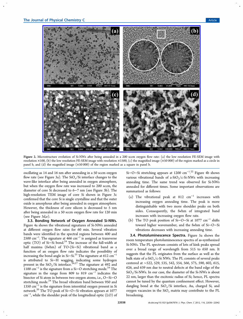
Figure 2. Microstructure evolution of Si-NWs after being annealed in a 200 sccm oxygen flow rate: (a) the low resolution FE-SEM image withresolution ×100, (b) the low resolution FE-SEM image with resolution ×1500, (c) the magnified image (×50 000) of the region marked as a circle inpanel b, and (d) the magnified image (×50 000) of the region marked as a square in panel b.
The Journal of Physical Chemistry C Article
dx.doi.org/10.1021/jp3067876 | J. Phys. Chem. C 2012, 116, 22036−2204222038

Figure 5b shows the PL spectra of Si-NWs annealed at 900°C in different oxygen flow rates. The asymmetric PL spectrumchanges to the symmetric PL spectrum after being annealed in
oxygen atmosphere. The PL of oxygen annealed Si-NWsspreads over from 515 to 530 nm, and the peak is centered at521.7 nm. The decrease of the fwhm of PL after oxygen
Figure 3. TEM images core−shell Si-NWs at different annealing conditions: (a) annealed in a 50 sccm oxygen flow rate for 60 min, (b) annealed in a200 sccm oxygen flow rate for 60 min, (c) the high-resolution TEM image of the region marked as a circle in panel b, (d,e) annealed in a 50 sccmoxygen flow rate for 120 min.
The Journal of Physical Chemistry C Article
dx.doi.org/10.1021/jp3067876 | J. Phys. Chem. C 2012, 116, 22036−2204222039

annealing is due to decreasing defect states in SiO2/Si-NWs.The integrated PL intensity increases with increasing O2 flowrate from 20 to 100 sccm but decreases above a 100 sccmoxygen flow rate. This could be due to the fact that defects(oxygen vacancies) are reduced as compared with whatappeared in the as-grown Si-NWs. Some important points areaddressed as follows:
(a) The main intrinsic defects (oxygen vacancies) of as-grown Si-NWs can be reduced by oxygen annealing. Thegreen emission in Si-NWs is known to be attributed tothe neutral vacancy in which the radiative recombinationof a photon-generated hole with an electron occupyingthe neutral vacancy is involved in the process.28,29
(b) The hydrogen is replaced by oxygen from the surface andthe interface of the Si-NWs during oxygen annealing.The oxygen point defects in Si-NWs could easily replaceO to generate deep level.30,31
The PL intensity of Si-NWs annealed at a 400 sccm O2 flowrate is still higher than a 20 sccm flow rate, indicating that the
nonradiative defects at the SiO2 and the SiO2/Si-NWs interfaceare lower than those at the native oxide shield Si-NWs. Anotherpossibility could be the quantum confinement of Si-NWs,
Figure 4. FTIR spectra of core−shell Si-NWs (a) annealed in adifferent oxygen flow rate for 60 min and (b) annealed in a 200 sccmoxygen flow rate for different annealing time.
Figure 5. Room-temperature photoluminescence spectra of Si-NWs(a) as-deposited, (b) annealed in a different oxygen flow rate for 60min, and (c) annealed in a 200 sccm oxygen flow rate for differentannealing time.
The Journal of Physical Chemistry C Article
dx.doi.org/10.1021/jp3067876 | J. Phys. Chem. C 2012, 116, 22036−2204222040
which arises when the diameter of Si-NWs is comparable withan exciton diameter after oxygen annealing. Figure 5c showsthat the Gaussian PL intensity decreases with increasingannealing time from 15 to 120 min. This indicates that O2annealing increases the surface states and roughness andintroduces a lot of vacancy states, which increase thenonoradiative recombination.3.5. UV−Vis-NIR Spectra. Figure 6 shows the reflection
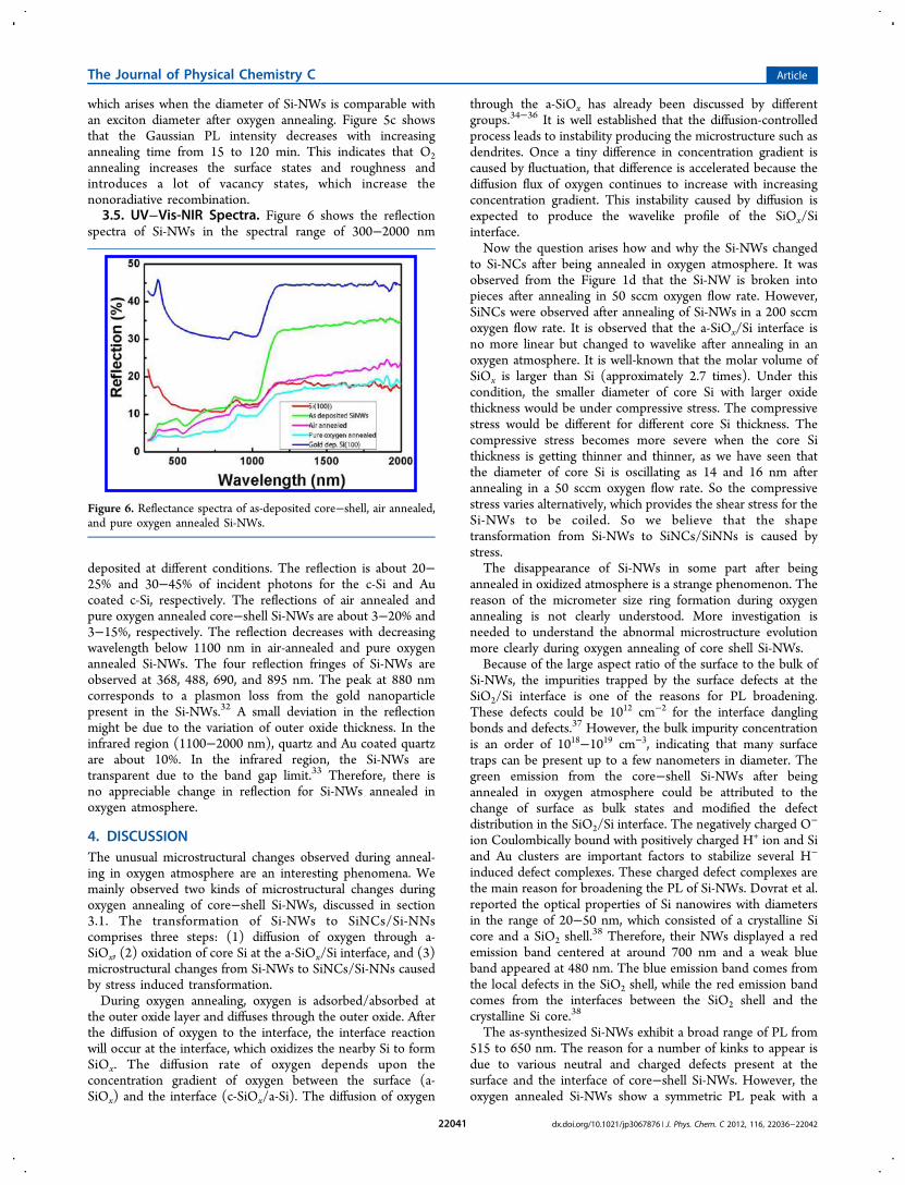
spectra of Si-NWs in the spectral range of 300−2000 nm
deposited at different conditions. The reflection is about 20−25% and 30−45% of incident photons for the c-Si and Aucoated c-Si, respectively. The reflections of air annealed andpure oxygen annealed core−shell Si-NWs are about 3−20% and3−15%, respectively. The reflection decreases with decreasingwavelength below 1100 nm in air-annealed and pure oxygenannealed Si-NWs. The four reflection fringes of Si-NWs areobserved at 368, 488, 690, and 895 nm. The peak at 880 nmcorresponds to a plasmon loss from the gold nanoparticlepresent in the Si-NWs.32 A small deviation in the reflectionmight be due to the variation of outer oxide thickness. In theinfrared region (1100−2000 nm), quartz and Au coated quartzare about 10%. In the infrared region, the Si-NWs aretransparent due to the band gap limit.33 Therefore, there isno appreciable change in reflection for Si-NWs annealed inoxygen atmosphere.
4. DISCUSSIONThe unusual microstructural changes observed during anneal-ing in oxygen atmosphere are an interesting phenomena. Wemainly observed two kinds of microstructural changes duringoxygen annealing of core−shell Si-NWs, discussed in section3.1. The transformation of Si-NWs to SiNCs/Si-NNscomprises three steps: (1) diffusion of oxygen through a-SiOx, (2) oxidation of core Si at the a-SiOx/Si interface, and (3)microstructural changes from Si-NWs to SiNCs/Si-NNs causedby stress induced transformation.During oxygen annealing, oxygen is adsorbed/absorbed at
the outer oxide layer and diffuses through the outer oxide. Afterthe diffusion of oxygen to the interface, the interface reactionwill occur at the interface, which oxidizes the nearby Si to formSiOx. The diffusion rate of oxygen depends upon theconcentration gradient of oxygen between the surface (a-SiOx) and the interface (c-SiOx/a-Si). The diffusion of oxygen
through the a-SiOx has already been discussed by differentgroups.34−36 It is well established that the diffusion-controlledprocess leads to instability producing the microstructure such asdendrites. Once a tiny difference in concentration gradient iscaused by fluctuation, that difference is accelerated because thediffusion flux of oxygen continues to increase with increasingconcentration gradient. This instability caused by diffusion isexpected to produce the wavelike profile of the SiOx/Siinterface.Now the question arises how and why the Si-NWs changed
to Si-NCs after being annealed in oxygen atmosphere. It wasobserved from the Figure 1d that the Si-NW is broken intopieces after annealing in 50 sccm oxygen flow rate. However,SiNCs were observed after annealing of Si-NWs in a 200 sccmoxygen flow rate. It is observed that the a-SiOx/Si interface isno more linear but changed to wavelike after annealing in anoxygen atmosphere. It is well-known that the molar volume ofSiOx is larger than Si (approximately 2.7 times). Under thiscondition, the smaller diameter of core Si with larger oxidethickness would be under compressive stress. The compressivestress would be different for different core Si thickness. Thecompressive stress becomes more severe when the core Sithickness is getting thinner and thinner, as we have seen thatthe diameter of core Si is oscillating as 14 and 16 nm afterannealing in a 50 sccm oxygen flow rate. So the compressivestress varies alternatively, which provides the shear stress for theSi-NWs to be coiled. So we believe that the shapetransformation from Si-NWs to SiNCs/SiNNs is caused bystress.The disappearance of Si-NWs in some part after being
annealed in oxidized atmosphere is a strange phenomenon. Thereason of the micrometer size ring formation during oxygenannealing is not clearly understood. More investigation isneeded to understand the abnormal microstructure evolutionmore clearly during oxygen annealing of core shell Si-NWs.Because of the large aspect ratio of the surface to the bulk of
Si-NWs, the impurities trapped by the surface defects at theSiO2/Si interface is one of the reasons for PL broadening.These defects could be 1012 cm−2 for the interface danglingbonds and defects.37 However, the bulk impurity concentrationis an order of 1018−1019 cm−3, indicating that many surfacetraps can be present up to a few nanometers in diameter. Thegreen emission from the core−shell Si-NWs after beingannealed in oxygen atmosphere could be attributed to thechange of surface as bulk states and modified the defectdistribution in the SiO2/Si interface. The negatively charged O
−
ion Coulombically bound with positively charged H+ ion and Siand Au clusters are important factors to stabilize several H−
induced defect complexes. These charged defect complexes arethe main reason for broadening the PL of Si-NWs. Dovrat et al.reported the optical properties of Si nanowires with diametersin the range of 20−50 nm, which consisted of a crystalline Sicore and a SiO2 shell.
38 Therefore, their NWs displayed a redemission band centered at around 700 nm and a weak blueband appeared at 480 nm. The blue emission band comes fromthe local defects in the SiO2 shell, while the red emission bandcomes from the interfaces between the SiO2 shell and thecrystalline Si core.38
The as-synthesized Si-NWs exhibit a broad range of PL from515 to 650 nm. The reason for a number of kinks to appear isdue to various neutral and charged defects present at thesurface and the interface of core−shell Si-NWs. However, theoxygen annealed Si-NWs show a symmetric PL peak with a
Figure 6. Reflectance spectra of as-deposited core−shell, air annealed,and pure oxygen annealed Si-NWs.
The Journal of Physical Chemistry C Article
dx.doi.org/10.1021/jp3067876 | J. Phys. Chem. C 2012, 116, 22036−2204222041

narrow range from 515 to 530 nm with the peak centered at521.7 nm. The PL shows a blue shift of 24 nm due to thedecrease in neutral oxygen vacancies. It can be inferred fromthe PL narrowing that the charge defect complex wasannihilated by oxygen annealing. Another reason might bethe stoichiometry altering after oxygen annealing, which isresponsible for the variation peak at a different oxygen flowrate.Although a blue shift of the PL peak from 545 to 521 nm is
observed after being annealed in an oxygen atmosphere, thepeak position is unchanged after being annealed in oxygenatmosphere irrespective of flow rate and annealing time.Moreover, the integrated intensity and their correspondingfwhm are modified after being annealed in oxygen atmosphere.In as-synthesized Si-NWs, the surface consists of Si−O and Sidangling bonds other than Au. Because of the stress, the Si−O−Si bonds partially break into Si−O, SiO, and Si−Hbonds, which might create a novel electronic state of theinterface.
5. CONCLUSIONSThe morphology of core−shell Si-NWs were changed fromstraight Si-NWs silicon to nanocoils (Si-NCs)/silicon andnanonoodles (Si-NNs) after annealing in oxygen atmosphere.FTIR study showed that the intensity increases as the Si-NWdiameter decreases. The as-synthesized Si-NWs showed a broadrange of visible emission, whereas a green emission wasobserved in core−shell Si-NWs after being annealed in oxygenatmosphere due to neutral oxygen vacancies.
■ AUTHOR INFORMATIONCorresponding Author*E-mail: [email protected] or [email protected] authors declare no competing financial interest.
■ ACKNOWLEDGMENTSThe financial support from BK21 program, Republic of Korea,is acknowledged. A part of this work is also funded by theKorea Science and Engineering Foundation (KOSEF) throughthe National Research Laboratory Program by Ministry ofScience and Technology (No. M10600000159-06J0000-15910).
■ REFERENCES(1) Chaudhuri, R. G.; Paria, S. Chem. Rev. 2011, 112, 2373−2433.(2) Su, L.; Jing, Y.; Zhou, Z. Nanoscale 2011, 3, 3967−3983.(3) Deng, Y. H.; Deng, C. H.; Qi, W.; Liu, C.; Liu, J.; Zhang, X. M.;Zhao, D. Adv. Mater. 2009, 21, 1377−1382.(4) Li, W.; Deng, Y.; Wu, Z.; Qian, X.; Yang, J.; Wang, Y.; Gu, D.;Zhang, F.; Tu, B.; Zhao, D. J. Am. Chem. Soc. 2011, 133, 15830−15833.(5) Deng, Y. H.; Cai, Y.; Sun, Z. K.; Zhao, D. Chem. Phys. Lett. 2011,510, 1−13.(6) Wu, Z.; Li, Q.; Feng, D.; Webley, P. A.; Zhao, D. J. Am. Chem.Soc. 2010, 132, 12042−12050.(7) Kelzenberg, M. D.; Evans, D. B. T.; Kayes, B. M.; Filler, M. A.;Putnam, M. C.; Lewis, N. S.; Atwater, H. A. Nano Lett. 2008, 8, 710−714.(8) Hyden, O.; Greytak, A. B.; Bell, D. C. Adv. Mater. 2005, 17, 701−704.(9) Seo, K.; Sharma, S.; Yasseri, A. Y.; Stewart, D. R.; Kamins, T. I.Electrochem. Solid State Lett. 2006, 9, G69−G72.(10) Sutardja, P.; Oldham, W. G. IEEE Trans. 1989, 36, 2415−2421.
(11) Xie, T.; Schmidt, V.; Pippel, E.; Senz, S.; Gcsele, U. Small 2008,4, 64−68.(12) Shia, X.; Kurstjensb, R.; Vosb, I.; Everaertb, J.; Schaekersc, M.ECS Trans. 2011, 34, 535−540.(13) Krylyuk, S.; Davydov, A. V.; Levin, I.; Motayed, A.; Vaudin, M.D. Appl. Phys. Lett. 2009, 94 (6), 063113.(14) Cui, H.; Wang, C. X.; Yang, G. W. Nano Lett. 2008, 8, 2731−2737.(15) Stan, G.; Krylyuk, S.; Davydov, A. V.; Cook, R. F. Nano Lett.2010, 10 (6), 2031−2037.(16) Sivakov, V. A.; Scholz, R.; Syrowatka, F.; Falk, F.; Gosele, U.;Christiansen, S. H. Nanotechnology 2009, 20, 405607−405607−8.(17) Fazzini, P. F.; Bonafos, C.; Claverie, A.; Hubert, A.; Ernst, T.;Respaud, M. J. Appl. Phys. 2011, 110, 033524.(18) Swain, B. S.; Swain, B. P.; Hwang, N. M. J. Phys. Chem. C 2010,114, 15274−15279.(19) Swain, B. S.; Lee, S. S.; Lee, S. H.; Swain, B. P.; Hwang, N. M.Chem. Phys. Lett. 2010, 494, 269−273.(20) Swain, B. S.; Swain, B. P.; Hwang, N. M. Curr. Appl. Phys. 2010,10, S439−S442.(21) Swain, B. S.; Swain, B. P.; Lee, S. S.; Hwang, N. M. J. Phys.Chem. C 2011, 115, 16745−16752.(22) Swain, B. S.; Swain, B. P.; Hwang, N. M. J. Appl. Phys. 2010,108, 073709.(23) Swain, B. S.; Lee, S. S.; Lee, S. H.; Swain, B. P.; Hwang, N. M. J.Cryst. Growth 2011, 327, 276−280.(24) Swain, B. P.; Dusane, R. O. Mater. Chem. Phys. 2006, 99, 240−246.(25) Swain, B. P. Appl. Surf. Sci. 2007, 253, 8695−8698.(26) Swain, B. P.; Swain, B. S.; Hwang, N. M. Appl. Surf. Sci. 2008,255, 2557−2560.(27) Swain, B. P.; Hwang, N. M. Appl. Surf. Sci. 2008, 254, 5319−5322.(28) Ruqeishi, M. S. A.; Nor, R. M.; Amin, Y. M.; Azri, K. A. Silicon2011, 3, 145−151.(29) Ruqeishi, M. S. A.; Nor, R. M.; Amin, Y. M.; Azri, K. A. Silicon2010, 2, 19−24.(30) Noe, P.; Guignard, J.; Gentile, P.; Delamadeleine, E.; Calvo, V.;Ferret, P.; Dhalluin, F.; Baron, T. J. Appl. Phys. 2007, 102, 016103.(31) Fukata, N.; Chen, J.; Sekiguchi, T.; Matsushita, S.; Oshima, T.;Uchida, N.; Murakami, K.; Tsurui, T.; Ito, S. Appl. Phys. Lett. 2007, 90,153117.(32) Niu, J. J.; Wang, J. N.; Chen, Y. X. Mater. Sci. Eng. B 2007, 139,95−98.(33) Faraci, G.; Gibilisco, S.; Pennisi, A. R.; Faraci, C. J. Appl. Phys.2011, 109, 074311−074311−4.(34) Narayanan, V.; Guha, S.; Copel1, M.; Bojarczuk, N. A.; Flaitz, P.L.; Gribelyuk, M. Appl. Phys. Lett. 2002, 81, 4183−4185.(35) Doremus, R. H. J. Phys. Chem. 1976, 80, 1773−1775.(36) Hoshino, T.; Hata, M.; Neya, S.; Nishioka1, Y.; Watanabe, T.;Tatsumura, K.; Ohdomari, I. J. Appl. Phys. 2003, 42, 3560−3565.(37) Pierreux, D.; Stesmans, A. Phys. Rev. B 2002, 66, 165320−165320−1.(38) Dovrat, M.; Arad, N.; Zhang, X. H.; Lee, S. T.; Saar, A. Phys. Rev.B 2007, 75, 205343−205347.
The Journal of Physical Chemistry C Article
dx.doi.org/10.1021/jp3067876 | J. Phys. Chem. C 2012, 116, 22036−2204222042
Copyright © 2022 FDOKUMEN