Optical properties of annealed silicon rich oxide (SRO) films
10
Optical properties of annealed silicon rich oxide (SRO) films A. Luna-López 1a , M. Aceves-Mijares, O. Malik, J. Pedraza and C. Falcony b a Department of Electronic, INAOE, Apdo. 51, Puebla, Pue. México 72000. b CINVESTAV, Depto. Física, Apdo. 17-740, México D.F., México 07000 ABSTRACT Silicon Rich Oxide (SRO) has luminescent properties that can be used in silicon optoelectronics devices. Nowadays the emission mechanisms are not completely understood, leading to a high potential field of research. The study of the SRO characteristics and its relation with the emission would provide information on the mechanism of radiation. In this work the optical properties of SRO are studied. Photoluminescence (PL), transmittance and refractive index of silicon rich oxide films annealed at high temperature during different times have been obtained. PL spectra show a considerable emission of visible light with different thermal treatment times and have a wide wavelength spectrum from 400 to 600 nm (3.1-2 eV ) and 650 to 850 nm (1.9-1.45 eV). Absorption spectra were studied and the optical band gap was determined. It can be seen that the optical band gap determined from these spectra changes as the silicon excess varies. The refractive index of SRO films also augments with the excess of silicon, and with the thermal treatments time. Keywords: Silicon Rich Oxide (SRO), Transmittance, Photoluminescence, refractive index, optical band gap, annealed. 1. INTRODUCTION Silicon is a material of indirect band, which makes it a poor light emitter. In the last decade, an intense research activity has been done taking different approaches to solve the physical inability of Si to act as a light emitter. Since the discovery of intense visible light emission in porous Si by Canham 1 , many researchers have studied the emission properties of materials made of Si. SRO has been one of them due to its interesting optics and electric characteristics, which varied with the Si excess contained in the films 2, 3 . The optical characteristics as refractive index of the SRO films can be varied on a range from 1.45 to 1.94, and the PL and absorption edge can fluctuate similarly with the excess silicon in the films, making SRO attractive to fabricate optoelectronic devices. These characteristics have given place to various types of applications as wave guides, no volatile memories, peaks suppressers, light radiation and detection devices 4, 5, 6, 7 etc. Due to the compatibility of SRO with the IC’s fabrication technology, Si optoelectronics integrated circuits can be developed in the next future. In the present work, PL, transmittance and refractive index characteristics of SRO films prepared by LPCVD are presented. The influence of the Ro (the ratio of reactive gases, which controls the silicon excess) and annealing temperature on these films are investigated. The optical characteristics to understand the possibly emission and absorption mechanism are studied. 2. EXPERIMENT SRO films were deposited on sapphire. SRO was deposited in a horizontal low-pressure CVD (LPCVD) hot-wall reactor using SiH 4 (Silane) and N 2 O (nitrous oxide) as reactive gases at 700 ºC. The flow ration, Ro = [N 2 O]/[SiH 4 ] = 10, 20 and 30, it was used to control the amount of excess silicon in the SRO films, and the pressure was varied for each Ro from 1.64- 1.94 Torr. The annealing was done at 1100 ºC in N 2 during 30, 60 and 180 minutes. Optical transmittance measurements were made in the range of the U-V to near infrared, NIR, at room temperature, using a spectrophotometer 1 Electronic mail : [email protected] ; phone + 52 (222) 2 47-20-11; fax +(52 222) 2 47-05-17
-
Upload
independent -
Category
Documents
-
view
0 -
download
0
Transcript of Optical properties of annealed silicon rich oxide (SRO) films
Optical properties of annealed silicon rich oxide (SRO) films
A. Luna-López1a, M. Aceves-Mijares, O. Malik, J. Pedraza and C. Falconyb
a Department of Electronic, INAOE, Apdo. 51, Puebla, Pue. México 72000. b CINVESTAV, Depto. Física, Apdo. 17-740, México D.F., México 07000
ABSTRACT
Silicon Rich Oxide (SRO) has luminescent properties that can be used in silicon optoelectronics devices. Nowadays the emission mechanisms are not completely understood, leading to a high potential field of research. The study of the SRO characteristics and its relation with the emission would provide information on the mechanism of radiation.
In this work the optical properties of SRO are studied. Photoluminescence (PL), transmittance and refractive index of silicon rich oxide films annealed at high temperature during different times have been obtained. PL spectra show a considerable emission of visible light with different thermal treatment times and have a wide wavelength spectrum from 400 to 600 nm (3.1-2 eV ) and 650 to 850 nm (1.9-1.45 eV). Absorption spectra were studied and the optical band gap was determined. It can be seen that the optical band gap determined from these spectra changes as the silicon excess varies. The refractive index of SRO films also augments with the excess of silicon, and with the thermal treatments time.
Keywords: Silicon Rich Oxide (SRO), Transmittance, Photoluminescence, refractive index, optical band gap, annealed.
1. INTRODUCTION
Silicon is a material of indirect band, which makes it a poor light emitter. In the last decade, an intense research activity has been done taking different approaches to solve the physical inability of Si to act as a light emitter. Since the discovery of intense visible light emission in porous Si by Canham1 , many researchers have studied the emission properties of materials made of Si. SRO has been one of them due to its interesting optics and electric characteristics, which varied with the Si excess contained in the films2, 3. The optical characteristics as refractive index of the SRO films can be varied on a range from 1.45 to 1.94, and the PL and absorption edge can fluctuate similarly with the excess silicon in the films, making SRO attractive to fabricate optoelectronic devices. These characteristics have given place to various types of applications as wave guides, no volatile memories, peaks suppressers, light radiation and detection devices4, 5, 6, 7 etc. Due to the compatibility of SRO with the IC’s fabrication technology, Si optoelectronics integrated circuits can be developed in the next future.
In the present work, PL, transmittance and refractive index characteristics of SRO films prepared by LPCVD are presented. The influence of the Ro (the ratio of reactive gases, which controls the silicon excess) and annealing temperature on these films are investigated. The optical characteristics to understand the possibly emission and absorption mechanism are studied.
2. EXPERIMENT
SRO films were deposited on sapphire. SRO was deposited in a horizontal low-pressure CVD (LPCVD) hot-wall reactor using SiH4 (Silane) and N2O (nitrous oxide) as reactive gases at 700 ºC. The flow ration, Ro = [N2O]/[SiH4] = 10, 20 and 30, it was used to control the amount of excess silicon in the SRO films, and the pressure was varied for each Ro from 1.64- 1.94 Torr. The annealing was done at 1100 ºC in N2 during 30, 60 and 180 minutes. Optical transmittance measurements were made in the range of the U-V to near infrared, NIR, at room temperature, using a spectrophotometer 1 Electronic mail : [email protected]; phone + 52 (222) 2 47-20-11; fax +(52 222) 2 47-05-17
Mariano Aceves
Proc. SPIE Vol. 6029 pp 88-97. Artículo 06015-17, 20th Congress of the International Commission for Optics
Jose Alberto Luna
Proc. SPIE / Volume 6029 / Materials and Nanostructures Optical properties of annealed silicon rich oxide (SRO) films Proc. SPIE, Vol. 6029, 60290E (2006); doi:10.1117/12.667675 Online Publication Date: 20 January 2006 Conference Title: ICO20: Materials and Nanostructures Conference Chairs: Wei Lu, Jeff Young
Perkin-Elmer LMBD 3B UV/VIS. The PL response was measured at room-temperature with a Perkin-Elmer LS-50B, with a pulse discharge xenon source, and as detector a multiplier tube. The PL detection was carried out from 400 to 900 nm with 2.5 nm resolution. The refractive index and the oxide thickness were measured with a null Ellipsometer Gaertner L117 with a laser of He-Ne (632.8 nm).
3. EXPERIMENTAL RESULTS
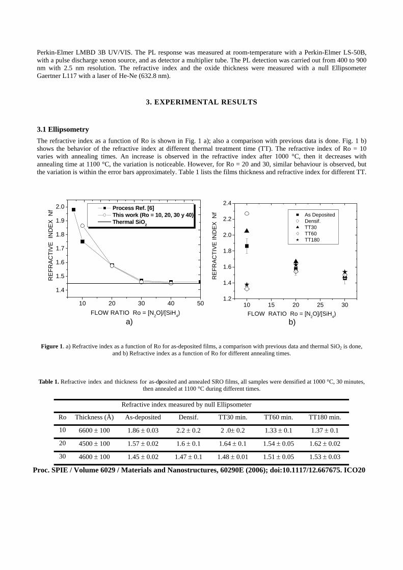
3.1 Ellipsometry The refractive index as a function of Ro is shown in Fig. 1 a); also a comparison with previous data is done. Fig. 1 b) shows the behavior of the refractive index at different thermal treatment time (TT). The refractive index of Ro = 10 varies with annealing times. An increase is observed in the refractive index after 1000 °C, then it decreases with annealing time at 1100 °C, the variation is noticeable. However, for Ro = 20 and 30, similar behaviour is observed, but the variation is within the error bars approximately. Table 1 lists the films thickness and refractive index for different TT.
10 20 30 40 50
1.4
1.5
1.6
1.7
1.8
1.9
2.0
FLOW RATIO Ro = [N2O]/[SiH4)
RE
FRA
CTI
VE
IN
DE
X N
f Process Ref. [6] This work (Ro = 10, 20, 30 y 40) Thermal SiO2
a)
10 15 20 25 301.2
1.4
1.6
1.8
2.0
2.2
2.4
FLOW RATIO Ro = [N2O]/[SiH4)
RE
FRA
CTI
VE
IND
EX
Nf As Deposited
Densif. TT30 TT60 TT180
b)
Figure 1. a) Refractive index as a function of Ro for as-deposited films, a comparison with previous data and thermal SiO2 is done, and b) Refractive index as a function of Ro for different annealing times.
Table 1. Refractive index and thickness for as-deposited and annealed SRO films, all samples were densified at 1000 °C, 30 minutes, then annealed at 1100 °C during different times.
Refractive index measured by null Ellipsometer
Ro Thickness (Å) As-deposited Densif. TT30 min. TT60 min. TT180 min.
10 6600 ± 100 1.86 ± 0.03 2.2 ± 0.2 2 .0± 0.2 1.33 ± 0.1 1.37 ± 0.1
20 4500 ± 100 1.57 ± 0.02 1.6 ± 0.1 1.64 ± 0.1 1.54 ± 0.05 1.62 ± 0.02
30 4600 ± 100 1.45 ± 0.02 1.47 ± 0.1 1.48 ± 0.01 1.51 ± 0.05 1.53 ± 0.03
Proc. SPIE / Volume 6029 / Materials and Nanostructures, 60290E (2006); doi:10.1117/12.667675. ICO20
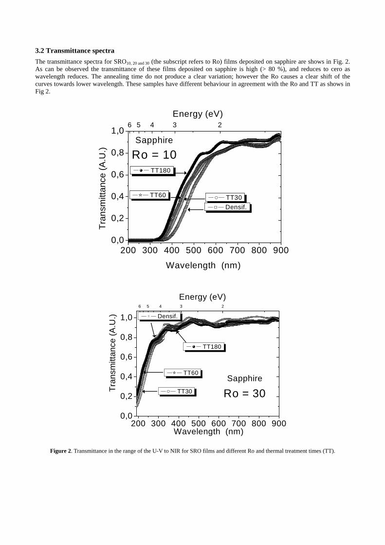
3.2 Transmittance spectra
The transmittance spectra for SRO10, 20 and 30 (the subscript refers to Ro) films deposited on sapphire are shows in Fig. 2. As can be observed the transmittance of these films deposited on sapphire is high (> 80 %), and reduces to cero as wavelength reduces. The annealing time do not produce a clear variation; however the Ro causes a clear shift of the curves towards lower wavelength. These samples have different behaviour in agreement with the Ro and TT as shows in Fig 2.
200 300 400 500 600 700 800 9000,0
0,2
0,4
0,6
0,8
1,06 5 4 3 2
TT60
TT180
TT30 Densif.
Sapphire
Ro = 10
Wavelength (nm)
Tran
smitt
ance
(A.U
.)Energy (eV)
200 300 400 500 600 700 800 9000,0
0,2
0,4
0,6
0,8
1,06 5 4 3 2
Energy (eV)
TT180
TT60
TT30
Densif.
Ro = 30Sapphire
Wavelength (nm)
Tran
smitt
ance
(A.U
.)
Figure 2. Transmittance in the range of the U-V to NIR for SRO films and different Ro and thermal treatment times (TT).
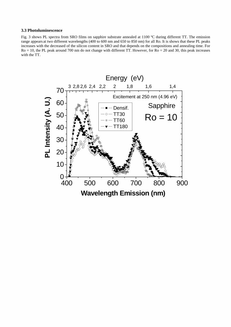
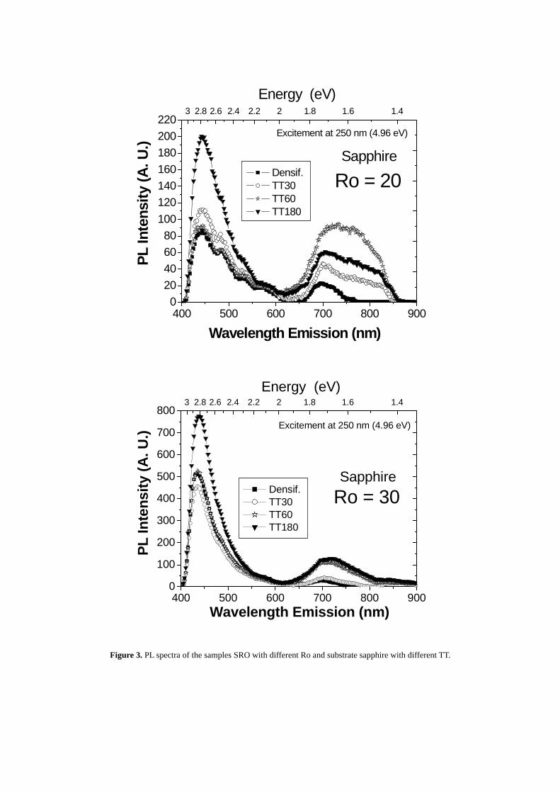
3.3 Photoluminescence Fig. 3 shows PL spectra from SRO films on sapphire substrate annealed at 1100 ºC during different TT. The emission range appears at two different wavelengths (400 to 600 nm and 650 to 850 nm) for all Ro. It is shows that these PL peaks increases with the decreased of the silicon content in SRO and that depends on the compositions and annealing time. For Ro = 10, the PL peak around 700 nm do not change with different TT. However, for Ro = 20 and 30, this peak increases with the TT.
400 500 600 700 800 9000
10
20
30
40
50
60
703 2,8 2,6 2,4 2,2 2 1,8 1,6 1,4
PL In
tens
ity (A
. U.)
Wavelength Emission (nm)
Densif. TT30 TT60 TT180
Ro = 10Sapphire
Excitement at 250 nm (4.96 eV)
Energy (eV)
400 500 600 700 800 9000
20406080
100120140160180200220
3 2.8 2.6 2.4 2.2 2 1.8 1.6 1.4
Energy (eV)
Excitement at 250 nm (4.96 eV)
Densif. TT30 TT60 TT180
Wavelength Emission (nm)
PL In
tens
ity (A
. U.)
Ro = 20Sapphire
400 500 600 700 800 9000
100
200
300
400
500
600
700
8003 2.8 2.6 2.4 2.2 2 1.8 1.6 1.4
Excitement at 250 nm (4.96 eV)
Energy (eV)
Densif. TT30 TT60 TT180
PL In
tens
ity (A
. U.)
Wavelength Emission (nm)
SapphireRo = 30
Figure 3. PL spectra of the samples SRO with different Ro and substrate sapphire with different TT.
4. DISCUSSION
4.1 Ellipsometry The refractive indexes of the SRO increase with the increase of excess Si. As Ro increases the index tends toward that of SiO2, and on the other way towards that of Si. Then, the inclusion of Si in these films is evident. After annealing, the refractive indexes varied without a clear tendency. Index for Ro= 10, however, has a bigger change, again no tendency is clearly depicted. In Atomic force microscope, AFM, studies of this material was observed that for SRO annealed at 1100 °C the surface was rough, and the roughness reduces as Ro increases. Being SRO10 the bumpiest compared to SRO20, 30, with hills as high as 50 nm for Ro = 10, and for Ro =30 are ten times smaller8. In Ref 9 it is shown that the thermal treatments at 1100 ºC in samples with a similar excess content as Ro=10 induce the formation of crystallites with a mean radius around of 1-5 nm detected with TEM, the nc-Si are homogeneously distributed in the film, except for a thin fully oxidized surface layer. The crystallites are related with the uneven surface observed in AFM. Then, the incident beam used to measure the thickness and refractive index disperses on the SRO surface, causing a spreading of the results. As Ro10 is the one with higher roughness, the results show a bigger variation. In addition, when thermal treatments are applied, a thin fully oxidized surface layer is formed and the refractive index try to decreased. Then, it is possible that ellipsometry is not an accurate technique to measure the thickness and refractive index of SRO films with high silicon excess. 4.2 Transmittance spectra
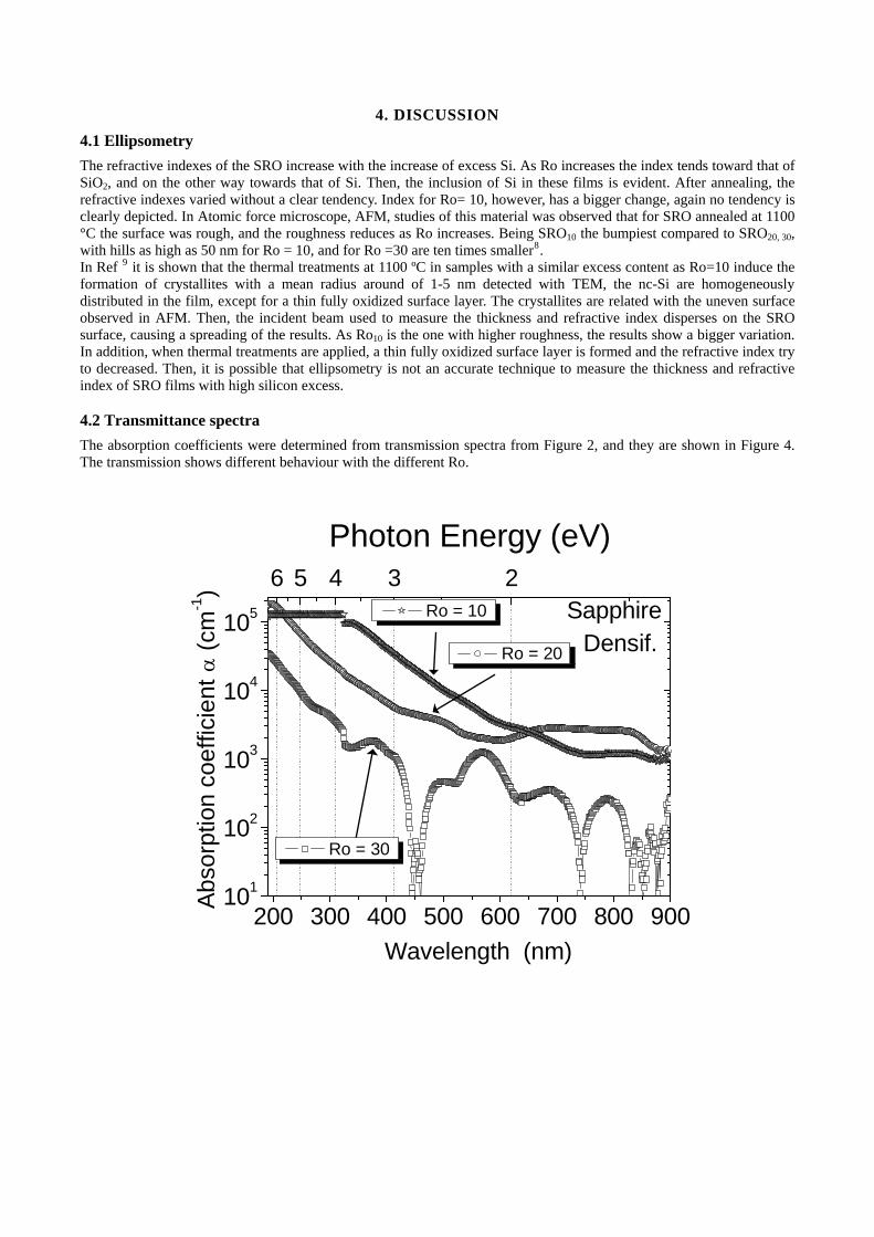
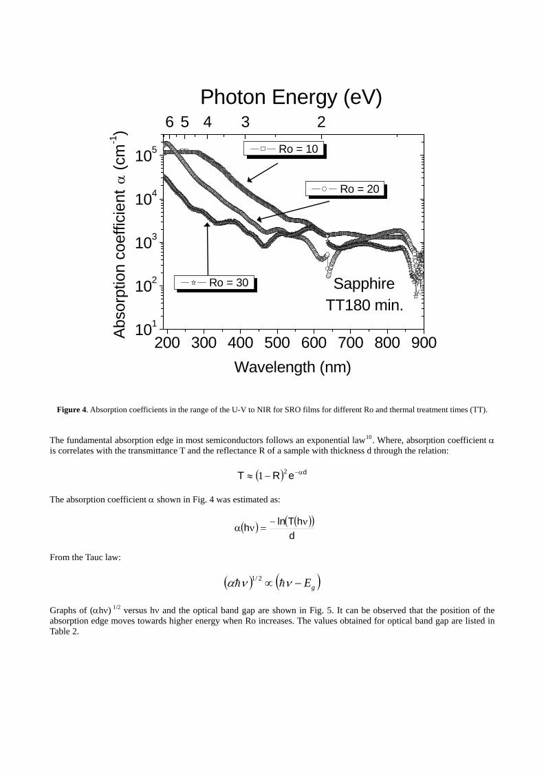
The absorption coefficients were determined from transmission spectra from Figure 2, and they are shown in Figure 4. The transmission shows different behaviour with the different Ro.
200 300 400 500 600 700 800 900101
102
103
104
105
6 5 4 3 2
Abso
rptio
n co
effic
ient
α (c
m-1)
Densif.Sapphire
Ro = 30
Ro = 20
Ro = 10
Wavelength (nm)
Photon Energy (eV)
200 300 400 500 600 700 800 900101
102
103
104
105
6 5 4 3 2
Ro = 30
Ro = 20
Ro = 10
Abso
rptio
n co
effic
ient
α (c
m-1)
Photon Energy (eV)
Wavelength (nm)
TT180 min.Sapphire
Figure 4. Absorption coefficients in the range of the U-V to NIR for SRO films for different Ro and thermal treatment times (TT).
The fundamental absorption edge in most semiconductors follows an exponential law10. Where, absorption coefficient α is correlates with the transmittance T and the reflectance R of a sample with thickness d through the relation:
( ) deRT α−−≈ 21
The absorption coefficient α shown in Fig. 4 was estimated as:
( ) ( )( )d
hTlnh ν−=να
From the Tauc law:
( ) ( )gE−∝ ννα 2/1
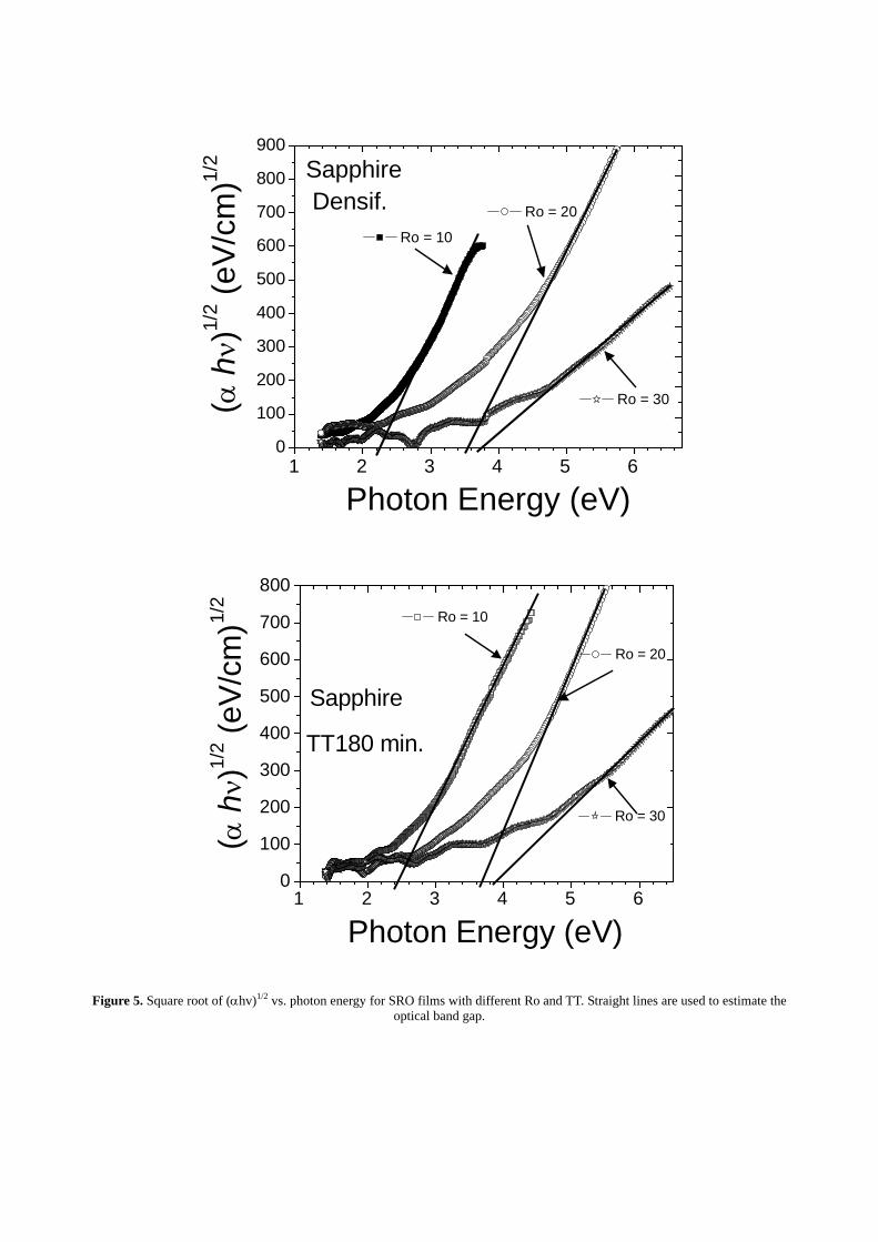
Graphs of (αhν) 1/2 versus hν and the optical band gap are shown in Fig. 5. It can be observed that the position of the absorption edge moves towards higher energy when Ro increases. The values obtained for optical band gap are listed in Table 2.
1 2 3 4 5 60
100
200
300
400
500
600
700
800
900
Densif.Sapphire
Ro = 30
Ro = 20
Ro = 10(α
hν)
1/2 (e
V/cm
)1/2
Photon Energy (eV)
1 2 3 4 5 60
100
200
300
400
500
600
700
800 Ro = 10
Ro = 30
Photon Energy (eV)
Ro = 20
(α hν)
1/2 (e
V/cm
)1/2
Sapphire
TT180 min.
Figure 5. Square root of (αhv)1/2 vs. photon energy for SRO films with different Ro and TT. Straight lines are used to estimate the
optical band gap.
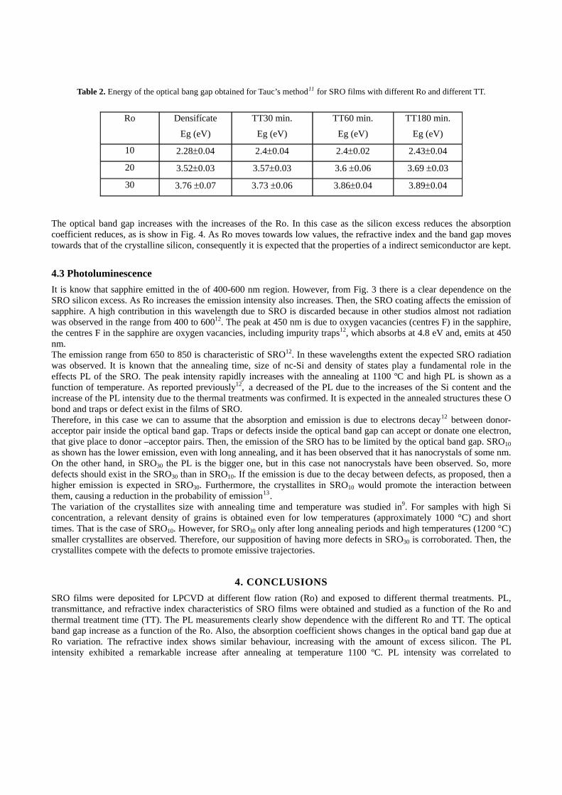
Table 2. Energy of the optical bang gap obtained for Tauc’s method11 for SRO films with different Ro and different TT.
Ro Densifícate
Eg (eV)
TT30 min.
Eg (eV)
TT60 min.
Eg (eV)
TT180 min.
Eg (eV)
10 2.28±0.04 2.4±0.04 2.4±0.02 2.43±0.04
20 3.52±0.03 3.57±0.03 3.6 ±0.06 3.69 ±0.03
30 3.76 ±0.07 3.73 ±0.06 3.86±0.04 3.89±0.04
The optical band gap increases with the increases of the Ro. In this case as the silicon excess reduces the absorption coefficient reduces, as is show in Fig. 4. As Ro moves towards low values, the refractive index and the band gap moves towards that of the crystalline silicon, consequently it is expected that the properties of a indirect semiconductor are kept. 4.3 Photoluminescence It is know that sapphire emitted in the of 400-600 nm region. However, from Fig. 3 there is a clear dependence on the SRO silicon excess. As Ro increases the emission intensity also increases. Then, the SRO coating affects the emission of sapphire. A high contribution in this wavelength due to SRO is discarded because in other studios almost not radiation was observed in the range from 400 to 60012. The peak at 450 nm is due to oxygen vacancies (centres F) in the sapphire, the centres F in the sapphire are oxygen vacancies, including impurity traps12, which absorbs at 4.8 eV and, emits at 450 nm. The emission range from 650 to 850 is characteristic of SRO12. In these wavelengths extent the expected SRO radiation was observed. It is known that the annealing time, size of nc-Si and density of states play a fundamental role in the effects PL of the SRO. The peak intensity rapidly increases with the annealing at 1100 ºC and high PL is shown as a function of temperature. As reported previously12, a decreased of the PL due to the increases of the Si content and the increase of the PL intensity due to the thermal treatments was confirmed. It is expected in the annealed structures these O bond and traps or defect exist in the films of SRO. Therefore, in this case we can to assume that the absorption and emission is due to electrons decay12 between donor-acceptor pair inside the optical band gap. Traps or defects inside the optical band gap can accept or donate one electron, that give place to donor –acceptor pairs. Then, the emission of the SRO has to be limited by the optical band gap. SRO10 as shown has the lower emission, even with long annealing, and it has been observed that it has nanocrystals of some nm. On the other hand, in SRO30 the PL is the bigger one, but in this case not nanocrystals have been observed. So, more defects should exist in the SRO30 than in SRO10. If the emission is due to the decay between defects, as proposed, then a higher emission is expected in SRO30. Furthermore, the crystallites in SRO10 would promote the interaction between them, causing a reduction in the probability of emission13. The variation of the crystallites size with annealing time and temperature was studied in9. For samples with high Si concentration, a relevant density of grains is obtained even for low temperatures (approximately 1000 °C) and short times. That is the case of SRO10. However, for SRO30 only after long annealing periods and high temperatures (1200 °C) smaller crystallites are observed. Therefore, our supposition of having more defects in SRO30 is corroborated. Then, the crystallites compete with the defects to promote emissive trajectories.
4. CONCLUSIONS SRO films were deposited for LPCVD at different flow ration (Ro) and exposed to different thermal treatments. PL, transmittance, and refractive index characteristics of SRO films were obtained and studied as a function of the Ro and thermal treatment time (TT). The PL measurements clearly show dependence with the different Ro and TT. The optical band gap increase as a function of the Ro. Also, the absorption coefficient shows changes in the optical band gap due at Ro variation. The refractive index shows similar behaviour, increasing with the amount of excess silicon. The PL intensity exhibited a remarkable increase after annealing at temperature 1100 ºC. PL intensity was correlated to
interaction between silicon islands and traps in the film depending on Ro and annealing. Refractive index increase as the excess of silicon increases. A big increment of the characteristic emission of sapphire was observed due to the SRO on it.
5. ACKNOWLEDGMENTS
We would like to thank CONACYT for providing support to this work. The authors also thank Pablo Alarcón, Mauro Landa, Carlos Zúñiga, Ignacio Juárez and Netzhualcoyotl Carlos for helping in the preparation of the samples.
6. REFERENCES
1. L. T. Canham, Appl. Phys. Letters, 57, 1046 (1990). 2. Di Maria, J. R. Kirtley, J. Pakulis, D. W. Dong, D. Kuan , F. L. Pesavento, T. N. Theis, N. Cutro, S. D. Brorson , “Electroluminescence studies in silicon dioxide films containing tiny silicon islands”, J. Appl. Phys. Vol. 56, No 2, 401-416, (1984). 3 . M. Aceves, C. Falcony, A. Reynoso, W. Calleja, A. Torres. “The conduction properties of the silicon /off – Stoichiometric SiO2 diode” Solid-State Electronics 39, 637 (1996). 4. D. J. DiMaria, D. W. Dong, F. L. Pesavento, “Enhanced conduction and minimized charge trapping in electrically alterable read-only memories using off-stoichiometric silicon dioxide films”, J. Appl. Phys. 1984; 55 (8): 3000-3019. 5. M. Aceves, A. Malik, and R. Murphy, The FTO/SRO/Si structure as a radiation sensor, In: Sensors and Chemometrics, editors: Maria Teresa Ramirez-Silva et al, Research Signpost, ISBN: 81-7736-067-1, 2001, p1-25. 6. F. Ay, A. Aydinly, “Comparative investigation of hydrogen bonding in silicon based PECVD grown dielectrics for optical waveguides”, Optical Materials, Vol. 26, Pag. 33-46, 2004. 7 . M. Aceves, D. Berman, J. Carranza, L. Berriel, C. Domínguez, “U V Silicon sensor using Si nanocrystals”, Nanotechnology, 2005-04-20,Anaheim, California USA, to be presented 8. Ed Heriberto Palomino, “Relación entre las características del SRO medidas mediante AFM, FTIR y FL", INAOE, thesis master, to be presented. 9. F. Iacona, G. Franzo and C. Spinella, J. Appl. Phys., 87, 1295 (2000) 10. J.I. Pankove, “Optical Processes in Semiconductors”, Dover New York, 1975 11. Zhixun Ma, Xianbo Liao, and Gonglin Kong et al, “Absorption spectra of nanocrystalline silicon embedded in SiO2 matrix”, Applied Physics Letters, Volume 75, number 13,1999. 12. D. Berman, M. Aceves, A, Gallegos, A. Morales, L. R. Berriel, J. Carrillo, F. Flores, C. Falcony, C. Domínguez, A. Llobera, M. Riera, and J. Pedraza, “Silicon excess and thermal annealing effects on the photoluminescence of SiO2 and silicon rich oxide super enriched with silicon implantation”, Phys. Stat. sol. © 1, No. S1, S83-S87, 2004. 13. D. J. DiMaria, D .W. Dong, F. L. Pesavento, 1984 J. Appl. Phys. 55(8), 3000-3019.