
Micro—and nano—X-ray beams
52
CHAPTER 9 9 Micro- and Nano-X-ray Beams Gema Martinez-Criado 1 , Elisa Borfecchia 2 , Lorenzo Mino 2 , Carlo Lamberti 2 1 Experiments Division, European Synchrotron Radiation Facility, 38043-Grenoble, France 2 Department of Chemistry, NIS Center of Excellence and INSTM Reference Center University of Turin, Via P. Giuria 7, I-10125 Torino, Italy Contents 1. Introduction 362 2. Basic Resolution Limits 363 2.1. Diffraction Limit 363 2.2. Geometrical Source Demagnification 364 2.3. Efficiency 365 2.4. Depth of Field 365 3. Advantages of Micro- and Nano-X-Ray Beams 365 4. XRM Modalities 367 4.1. Full-Field X-Ray Microscope 367 4.2. Scanning X-Ray Microscope 368 4.3. Summary 369 5. X-Ray Focusing Optics 370 5.1. Refractive Optics 370 5.1.1. Compound Refractive Lenses 370 5.1.2. Adiabatically Focusing Lenses 372 5.2. Reflective Optics 373 5.2.1. Capillaries 373 5.2.2. KB Mirrors 374 5.2.3. Montel (or Nested KB) Mirrors 377 5.3. Diffractive Optics 378 5.3.1. Fresnel Zone Plates 378 5.3.2. Multilayer Laue Lenses 379 5.3.3. Kinoform Fresnel Lenses 380 5.4. Summary 381 6. Analytical Methods 383 7. Applications 385 7.1. Cluster Formation 385 7.2. Morphological Defects 388 7.3. Short-Range Order 390 7.4. Ion Implantation in Single Nanowires 392 7.5. Breakdown Sites in Photovoltaic Materials 394 Characterization of Semiconductor Heterostructures and Nanostructures Second Edition (C. Lamberti and G. Agostini Eds.) Ó 2013 Elsevier B.V. ISBN 978-0-444-59551-5, http://dx.doi.org/10.1016/B978-0-444-59551-5.00009-1 All rights reserved. 361
-
Upload
independent -
Category
Documents
-
view
3 -
download
0
Transcript of Micro—and nano—X-ray beams
CHAPTER99Micro- and Nano-X-ray Beams
Gema Martinez-Criado1, Elisa Borfecchia2, Lorenzo Mino2, Carlo Lamberti21Experiments Division, European Synchrotron Radiation Facility, 38043-Grenoble, France2Department of Chemistry, NIS Center of Excellence and INSTM Reference Center University of Turin, Via P. Giuria 7,
I-10125 Torino, Italy
Contents
1. Introduction 362
2. Basic Resolution Limits 363
2.1. Diffraction Limit 363
2.2. Geometrical Source Demagnification 364
2.3. Efficiency 365
2.4. Depth of Field 365
3. Advantages of Micro- and Nano-X-Ray Beams 365
4. XRM Modalities 367
4.1. Full-Field X-Ray Microscope 367
4.2. Scanning X-Ray Microscope 368
4.3. Summary 369
5. X-Ray Focusing Optics 370
5.1. Refractive Optics 370
5.1.1. Compound Refractive Lenses 370
5.1.2. Adiabatically Focusing Lenses 372
5.2. Reflective Optics 373
5.2.1. Capillaries 373
5.2.2. KB Mirrors 374
5.2.3. Montel (or Nested KB) Mirrors 377
5.3. Diffractive Optics 378
5.3.1. Fresnel Zone Plates 378
5.3.2. Multilayer Laue Lenses 379
5.3.3. Kinoform Fresnel Lenses 380
5.4. Summary 381
6. Analytical Methods 383
7. Applications 385
7.1. Cluster Formation 385
7.2. Morphological Defects 388
7.3. Short-Range Order 390
7.4. Ion Implantation in Single Nanowires 392
7.5. Breakdown Sites in Photovoltaic Materials 394
Characterization of Semiconductor Heterostructures and Nanostructures
Second Edition (C. Lamberti and G. Agostini Eds.) 2013 Elsevier B.V.
ISBN 978-0-444-59551-5, http://dx.doi.org/10.1016/B978-0-444-59551-5.00009-1 All rights reserved.361

7.6. Compositional/Structural Gradients in Monolithic Device Integration 395
7.7. Scanning X-Ray Diffraction Imaging of Individual SiGe/Si Islands 397
7.8. Local Structure of Single Semiconductor Rolled-Up Nanotubes 401
7.9. Local Strain Characterization in Microelectronic Materials and Devices 404
8. Summary and Future Perspectives 407
References 407
1. INTRODUCTION
Although existing X-ray instruments have already contributed to the rapid advancement
of semiconductors, as demonstrated in the previous chapters (3-8), in some cases, there
are strong limitations in terms of spatial resolution and sensitivity (i.e. signal/background
ratio). Micro- and/or nanometer-scale spatial resolving power added to X-ray absorp-
tion spectroscopy (XAS), X-ray diffraction (XRD), or X-ray scattering techniques is
strongly appreciated in semiconductor research for three reasons. First, the study of
micro/nanoscale objects, small embedded domains with weak signals and/or hetero-
geneous structures at the (sub)micrometer scales requires the use of intense X-ray pencil
beams, sometimes even in real time. Over the past two decades, the spatial resolution has
improved drastically down to 15e50 nm beams [1,2].
Although, in principle, a pinhole could do this task, the resulting X-ray photon flux is
extremely low for most practical purposes. Narrow apertures are only efficient if the beam
divergence on to the aperture exceeds the diffraction limited divergence.As a consequence,
they have frequently beenused in combinationwith condensing optics. Second, stimulated
by the great brilliance with reduced emittance of current third-generation synchrotron
sources [3], and new developments in X-ray detector technology (such as fast-readout
large-area detectors with high dynamic range and low noise characteristics) [4], today
intense (sub)micron X-ray beams are available with a variety of focusing devices including
Fresnel zone plates (FZP) [5], compound refractive lens (CRL) [6], KirkpatrickeBaez
(KB) mirrors [7] and tapered capillaries [8,9]. Third, thanks to the multiple interactions of
X-rays with matter, these X-ray microprobes can be used for manifold purposes, such as
ultrasensitive elemental/chemical detection using X-ray fluorescence (XRF)/X-ray
absorption [10], or for identification of minority phases [11], and/or strain fields by XRD
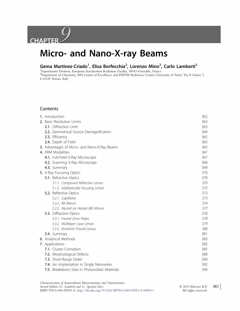
with (sub)micron resolution [12] (Fig. 9.1). In this chapter, advancedmethods for forming
micro- and nano-X-ray beams are reviewed, the merits of each experimental approach are
discussed and recent scientific examples are briefly described. Small angle X-ray scattering
(SAXS) experiments with micro-beams are described in Section 5 of Chapter 4 and in
Section 3.7 of Chapter 5.
For editorial reasons, in this chapter, we will deal with the use of hard X-rays only.
We will show examples of the use of X-ray microscopy (XRM) in the determination of
space-resolved structural (XRD) and electronic (X-ray absorption near edge structure
(XANES)/Extended X-ray absorption fine structure (EXAFS)) properties and in the
362 Gema Martinez-Criado, Elisa Borfecchia, Lorenzo Mino, Carlo Lamberti
chemical speciation (XRF) of nanostructured or composite materials. Photoemission
spectromicroscopy will be discussed in Section 4 of Chapter 14. Examples of spatial-
resolved Raman studies are reported in Sections 3.1, 3.5, 3.6 and 3.7 of Chapter 17,
while Sections 2.2, 2.3 of the same chapter discuss the experimental set-ups needed to
perform the experiments.
2. BASIC RESOLUTION LIMITS
In this section, some quantities used to compare and to characterize the different X-ray
focusing optics are briefly summarized.
2.1. Diffraction Limit
The transverse resolution of any X-ray optical element is limited by diffraction and can
be estimated by the Rayleigh’s criterion [13]:
sDL ¼ gl=NA [9.1]
where l is the wavelength and NA is the numerical aperture of the lens. g equals 0.61 for
two-dimensional focusing by a round lens, whereas for a linear (or rectangular) lens, g
equals 0.5. With an opening angle of q, the numerical aperture can be expressed by
NA ¼ n sin q [9.2]
Figure 9.1 Role of the advanced X-ray analytical techniques with micro- and nano-beams for semi-conductor materials, including future goal and target. Unpublished figure. For color version of thisfigure, the reader is referred to the online version of this book.
Micro- and Nano-X-ray Beams 363
where n is the index of refraction at wavelength l of the medium between the object
and the image. Although, in principle, spatial resolutions in the nanometer scale could
be reached using the short wavelength in the hard X-ray regime, the major limitation in
X-ray optics remains the low achievable numerical aperture. The latter is caused by the
weak interaction of high-energy photons with matter, as expressed by the complex index
of refraction:
n ¼ 1! dþ ib [9.3]
where d describes the dispersion and b the absorption in the material. d is of the order
10!5 in solid materials and only around 10!8 in air. The imaginary part b is usually much
smaller than d. As a consequence, NA z q, which means that for a wavelength of 1 A,
for example, a numerical aperture of about 0.06 is necessary to reach 1-nm resolution.
Between 2000 and 2010, there have been tremendous fabrication efforts to increase the
numerical aperture as discussed later.
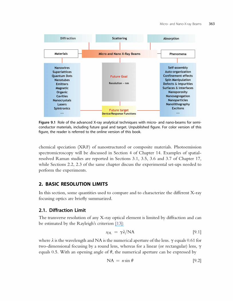
2.2. Geometrical Source Demagnification
In addition to the diffraction limit, the focusing is limited by geometrical source
demagnification,
sG ¼ S # q=p [9.4]
where S is the size of the source, q is the distance from the focusing element to the focal
spot, and p is the distance from the source to the focusing element (Fig. 9.2). Equation
[9.4] shows that the longer the source distance, the smaller the focal size obtained. Thus,
the development of long beamlines allows today large source size demagnifications
(emblematic in this regard is the construction of a 1 km long beamline at the Japanese
synchrotron Spring-8) [14].
Additionally, real optics are also restricted by imperfections like aberrations, mirror
shape errors, roughness or nonuniform areas, as well as further experimental issues such
as vibrations, drifts, etc. [15,16]. Therefore, several factors contribute to limiting the
final-point spread function: the diffraction limit (sDL), geometrical source demagnifi-
cation (sG), and imperfections (sI). So, the full width at half maximum (FWHM) limit of
the resolution (s) is a convolution of all these contributions, approximated by
swffiffiffiffiffiffiffiffiffiffiffiffiffiffiffiffiffiffiffiffiffiffiffiffiffiffiffiffiffiffi
sG2 þ sDL2 þ sI2p
[9.5]
Figure 9.2 Schematic of theoptical demagnification, obey-ing the Gaussian lens formula.Unpublished figure. For colorversion of this figure, thereader is referred to the onlineversion of this book.
364 Gema Martinez-Criado, Elisa Borfecchia, Lorenzo Mino, Carlo Lamberti
2.3. Efficiency
Most of the real focusing devices do not transmit the entire flux incident on the X-ray
focusing optic into the focal spot. Thus, the transmission efficiency can be defined as the
ratio of the intensity of the X-ray beam emerging from the lens, It, to the intensity of the
X-ray beam incident on the X-ray focusing optics Io:
ε ¼ It=Io [9.6]
In general, X-ray mirror systems present higher efficiencies (50e90%) than refractive
and diffractive lenses (typically between 10 and 40%). For refractive lenses, the lower
efficiency is mainly due to the large material absorption. Otherwise, in the case of
diffractive optics, the main cause for efficiency reduction is the scattering of incident
intensity into other diffraction orders (both positive and negative), which are excluded
from contributing to the first-order focus by the order sorting aperture.
2.4. Depth of Field
The longitudinal resolution, or depth of field (DoF), describes the distance between two
object points along the optical axis and can be expressed by
DoFzl=NA2 [9.7]
where l is the wavelength and NA is the numerical aperture of the lens. This magnitude
sets practical constraints on the sample thickness. For tomography, a long depth of field is
also advantageous. In that context, the focusing tolerance, commonly called depth of
focus, represents the probing length where the lateral beam size is nearly constant. For
example, an X-ray microbeam generated by refractive lenses can have a depth of focus in
the millimeter length scale, whereas for nanofocusing reflective optics, it can be in the
micrometer range.
3. ADVANTAGES OF MICRO- AND NANO-X-RAY BEAMS
Although table-top X-ray microscopes have recently been demonstrated [17], the
production of highly intense micro- and nano-X-ray beams is mostly oriented to
synchrotron radiation facilities because of several factors. From a scientific point of
view, such sources could make possible to probe deeply into inner grains embedded in
materials, buried heterostructures, small particles or microdomains by characterizing
simultaneously many properties in situ, the micro- and nano-structure in two and
three dimensions, or the evolution during processes (such as materials deposition and
gas-phase chemical reactions), as well as under operating conditions (e.g. temperature
cycling, high electric fields). From a technical perspective, third-generation
synchrotron sources deliver very small (better than 50 mm), well collimated and intense
X-rays beams with several orders of magnitude more photon flux than lab sources,
Micro- and Nano-X-ray Beams 365

ranging from the soft to the hard X-ray energy regime. Thus, key source requirements
can easily be fulfilled for an X-ray microscope, such as energy tunability (e.g. for
scattering or diffraction, and XAS energy scans, requiring to span a range of w1 keV
in energy), bandwidth (w10!2e10!4), high photon flux, spectral purity (harmon-
ics< 0.1%), low emittance (spot sizeediffraction limited) as well as excellent stability.
Therefore, with outstanding brilliance, transverse coherence and polarization,
synchrotron radiation micro- and nano-beams have several advantages over optical,
electron and neutron probes. First, the ultimate resolution sDL for X-ray microscopes
according to Eqn [9.1] should be almost two orders of magnitude below the achieved
resolution by light microscopy. Although the electron microscopes in all operation
modes (scanning electron microscope (SEM), scanning transmission electron micro-
scope (STEM), tomography, energy dispersive X-ray spectroscopy, electron energy loss
spectroscopy (EELS)) are essential high-resolution tools, they are restricted to very thin
sections and surface observations. Second, due to the large penetrating power, XRM is
able to noninvasively obtain information from thick samples demanding little or no
specimen preparation even under in situ conditions, which is impossible in electron
microscopy. Although this high penetration of X-rays makes sometimes the produc-
tion of high-resolution lenses challenging, unlike “lensless” imaging methods like
coherent diffraction imaging [18], the XRM also offers a general instrument with rich
image-contrast mechanisms (e.g. absorption, chemical state, phase, diffraction,
polarization) to obtain images, zoom into regions of interest and build up large fields of
view of specimens within minutes rather than hours. Finally, although it shares most of
the advantages with neutron microscopy [19], this latter potential competitor currently
suffers from the lack of sufficiently bright sources. Table 9.1 reports the order of
Table 9.1 Comparison of different types of microscopies: X-ray microscopy (XRM); visible lightmicroscopy (VLM); scanning electron microscopy (SEM); transmission electron microscopy (TEM).Reported values are only qualitative. For photon based microcopies the wavelength is given by l¼ hc/
E¼ [12.3984 (Å keV)]/E¼ [1.23984 (mm eV)]/E, being E the photon energy, c the speed of light and h thePlanck constant. For electron based microcopies it is given by the de Broglie equation: l ¼ h/p, beingthe electron momentum
XRM VLM SEM TEM
Wavelength
range
~0.03e50 nm 400e800 nm 0.006e0.08 nm 0.002e0.004 nm
Current
resolution
20 nm 200 nm 1e10 nm 0.1 nm
Penetration
depth
1e50 mm
(E < 10 keV)
20 mm
(E ¼ 100 keV)
<100 nm
(metals)
<10 nm
(typically)
<3 mm (EDX)
<100 nm
Vacuum needed No No Yes Yes
Sample
preparation
No No Yes Yes
366 Gema Martinez-Criado, Elisa Borfecchia, Lorenzo Mino, Carlo Lamberti

magnitude of the wavelength used, of the spatial resolution, of the penetration depth
and some technical requirements of the different microscopies.
Therefore, as a general trend, conventional powerful techniques such as XRD, XRF,
and XAS have been evolving toward microscale and nanoscale versions. Already today,
individual micrograins within a polycrystalline sample can be isolated with the use of
micro-X-ray beams [20]. XRD is commonly employed to elucidate the local structural
features and can be combined with XRF to provide element specificity on appropriate
length scales [21].
4. XRM MODALITIES
In general, several XRM layouts can be found currently in operation, depending on the
energy of the X-ray beam (soft or hard X-rays), the specific setup (surface- or bulk-
sensitive), the nature of the specimen (magnetic materials, organic or biological speci-
mens) and/or detected signal from it; for example, the scanning transmission X-ray
microscope (TXM), the scanning photoemission microscope, the scanning X-ray
fluorescence microscope, the photoemission electron microscope or the full-field TXM.
However, X-ray microscopes are generally grouped into two classes so far: full-field
X-ray microscopes and scanning X-ray microscopes (SXM) [22].
In the following sections, these microscopes are reviewed and compared in
more detail, focusing on the best experimental setup for each sample to investigate. In
Section 7, the capabilities of the scanning X-ray microscope are specifically illustrated in
different examples.
4.1. Full-Field X-Ray Microscope
This approach uses an optical arrangement similar to the classical light and transmission
electron microscopes (Fig. 9.3): optical elements as objectives to create magnified images
of the objects [23]. The condenser illuminates the sample and an objective lens magnifies
the image of the sample into a fast charge-coupled device (CCD) camera allowing
detection in the millisecond timescale [24]. By positioning the sample close to the focal
distance, higher magnifications can be achieved using projection XRM. Thus, the
Figure 9.3 Optical sche-matic of the full-fieldX-ray microscope. Unpub-lished figure. For colorversion of this figure, thereader is referred to theonlineversionof thisbook.
Micro- and Nano-X-ray Beams 367

magnified projection image of the object is formed on the 2D detector with a magni-
fication that is equal to the ratio of the opticsedetector and objecteoptics distances, see
Fig. 9.3. This flexible scheme could also be adapted for absorption/phase-contrast
imaging. By rotating the sample, a series of projection images at different angles can be
acquired, from which the internal 3D electronic density can be determined using
tomographic reconstruction algorithms. Although full-field TXM are generally fast with
relatively simple instrumentation and high spatial resolution, their relative inefficiency
implies the use of high X-ray photon doses. Moreover, they are limited in acquiring
chemical information (space resolved XRF spectra cannot be collected), but XANES
imaging can be performed scanning the energy of the incoming beam across an
absorption edge and measuring the transmitted X-ray beam [25a] (Fig. 9.3). With this
experimental setup the incoming beam intensity, needed to obtain a XANES spectrum,
see Eq. [7.18] in Chapter 7 [25b], is collected a posteriori, after having removed the sample
from the beam [25c].
4.2. Scanning X-Ray Microscope
The scanning XRM, on the other hand, uses a focusing optics to form a finely focused
spot through which the sample is raster-scanned on pixel-by-pixel base across the
microprobe [26] (Fig. 9.4). This approach allows concurrent acquisition of different
signals by multiple detectors (for example, combining XRD, XRF and/or XAS).
Accordingly, it can make simultaneous analyses of the crystallographic orientation,
elemental or chemical distribution possible within inhomogeneous specimens with
submicron resolution [27]. In general terms, the scanning X-ray microscopes are effi-
cient in terms of X-ray photon doses (i.e. a high tradeoff between X-ray photon flux
and signal-to-noise ratio) and suitable for multimodal imaging, see Fig. 9.4. However,
they are slow because motors have to move the sample point by point in the focus point
of the beam in order to sample the desired area (scan rates range from a few hundred
seconds to a few hours, depending upon the image dimensions, spatial resolution and
element dilution). Moreover, they need complex instrumentation (e.g. multi-element
Figure 9.4 Optical schematic of the scanning X-ray microscope. Unpublished figure. For color versionof this figure, the reader is referred to the online version of this book.
368 Gema Martinez-Criado, Elisa Borfecchia, Lorenzo Mino, Carlo Lamberti

fluorescence detector, large-area CCD camera, XYZ translation stage with continuous
rotation about an axis). In addition, its nonstatic operation mode can affect the lateral
resolution due to sample placement accuracy.
4.3. Summary
Both instruments are complementary to each other and have their advantages and
disadvantages [28]. In the full-field TXM, as mentioned, the lens behind the sample
limits the efficiency, so only few photons arriving at the sample contribute to the image
formation. Thus, the TXM compared to SXM needs a higher photon dose because of
the low efficiency of the objective lens. In the scanning X-ray microscope, on the other
hand, a low-noise diffraction camera can also be used in transmission mode. Moreover,
the information availability, not restricted to transmission imaging, can be multiplied by
simultaneously measuring different secondary effects, such as XRF, total electron yield
(TEY), X-ray excited optical luminescence (XEOL). As a counterpart, a scanning X-ray
microscope requires much higher brilliant and coherent sources than full-field TXM to
keep the acquisition time reasonable. Finally, sorting by energy, the microfocusing optics
of a hard X-ray microscope allows longer focal lengths (up to more than a meter) and
larger depth of field (up to a few millimeters) than a soft X-ray microscope. This
capability is advantageous for the use of specific sample environments like furnaces or
high-pressure cells. Also, a shorter wavelength is favorable for X-ray diffraction studies
including wide- and small-angle scattering approaches.
Table 9.2 summarizes both types of X-ray microscopes available today. In all these
setups, focusing devices are needed and the achieved spatial resolution depends on the
performance of optical elements.
To close, once the tipology of X-ray microscope to use has been defined, the prac-
tically achievable X-ray beam characteristics depend on the X-ray wavelength, source
dimension, as well as type and quality of the optical element employed. In general, the
beam size can be reduced by scaling down the source size or by increasing the demag-
nification ratio, either by setting up the microscope at a larger distance from the source or
by reducing the focal distance. This latter approach is particularly useful since the
numerical aperture can be increased together with the demagnification ratio, reducing the
diffraction limited focus size and increasing the photon density in the focus. Therefore,
Table 9.2 Summary of the characteristics of full-field and scanning X-ray microscopesFull-field X-ray microscope Scanning X-ray microscope
Resolution (nm) 100e1000 20e1000
Contrast mechanisms Absorption/Phase/XANES Absorption/XRF/XRD/
XANES/EXAFS/Photoemission
Photon dose required High Low
Throughput High Low
Micro- and Nano-X-ray Beams 369

the working distance q, and thus, the overall length of the beamline must also be
considered carefully. Presently, many third-generation synchrotron facilities are devel-
oping long beamlines (e.g. 150 me1 km) with small secondary source (~25 mm slit),
allowing the source size to be fully exploited in both dimensions [14,29,30], while
keeping the working distance large enough to accommodate in situ experiments.
Although a smaller X-ray beam could also be produced in theory using a more
complicated optical arrangement on a shorter beamline, in practice, however, the number
of X-ray optical components should be restricted whenever possible to minimize beam
degradation from sources such as mirror slope errors, absorption in refractive elements,
thermal/vibration instability [15]. Apart from the minimum spot size/maximum flux
criteria, usually other arguments, such as availability, simplicity of use and cost, influence
the final choice of X-ray microscope. Finally, the radiation damage of the specimen under
such a high-flux X-ray beam determines the sample environment (e.g. liquid nitrogen)
and/or the use of a specific focusing device [28].
5. X-RAY FOCUSING OPTICS
Several focusing schemes have been developed for X-ray microscopes so far. In general,
X-ray beams can reach spot sizes from micrometers down to tens of nanometers using
three approaches [1]: refractive, reflective and diffractive optics. Most of them are
available as standard beamline components, even commercially.
5.1. Refractive Optics
5.1.1. Compound Refractive Lenses
In terms of refraction effects, there are two basic differences between X-rays and visible
light. First, according to Eqn [9.3], the tiny deviation in the index of refraction from
unity is of the order of 10!5 compared to visible light in glass (n ~ 1.5). As a result, the
focal length of a single X-ray lens with a 2 mm radius of curvature can be of order 100 m,
which is too long for most practical applications. However, if many single lenses are
stacked behind one another, they form a CRL, which presents a reduced focal length of
manageable size [31]. Second, because the refractive index deviation is negative, X-ray
lens shapes must be concave instead of convex, typically used for optical lenses. Since the
very beginning, Snigirev et al. showed that cylindrical CRLs can be made with a focal
length in the meter and a focal spot size in the micrometer range (Fig. 9.5). Later, the
introduction of a parabolic lens profile,
s2 ¼ 2Ru [9.8]
made them free of spherical aberrations, with focal lengths given by
f ¼ R=2Nd [9.9]
370 Gema Martinez-Criado, Elisa Borfecchia, Lorenzo Mino, Carlo Lamberti

where N is the number of stacked lenses, R, the radius of curvature at the apex of the
parabola, and d, the real-part decrement of the index of refraction [32]. However, their
spatial resolution was limited by absorption, finite aperture and surface roughness.
Applying the Gauss lens formula, relationship among the source distance p, image
distance q and focal length f via
1=f ¼ 1=pþ 1=q [9.10]
the diffraction-limited resolution sDL of a biconcave lens with aperture
2R0 ¼ 2ð2Ru0Þ1=2 [9.11]
is given by the effective aperture Aeff of the lens reduced by photon absorption and
scattering
NA ¼ Aeff =ð2qÞ [9.12]
compared to the geometrical aperture 2R0. Recent simulations performed by Sanchez
del Rio et al. to obtain the ideal Gaussian focus [33] have suggested that the use of
lenses with a Cartesian oval profile could reduce aberrations in highly demagnifying
optics.
Despite its chromaticity and strong absorption that causes an efficiency decrease,
CRLs present many advantages. In general, they are in-line compact optics characterized
by an easy alignment, high stability under high heat load operation, adjustable focus, as
well as fewer perturbations due to surface roughness than grazing-incidence X-ray
optics. Although choosing a low-Z material such as lithium, beryllium, boron or dia-
mond can improve the efficiency and resolution, nanofabrication techniques are still
crucial to produce extremely small radii of curvature [34]. For instance, parabolic
refractive nanofocusing lenses have been developed with a focal distance of about 10 mm
and a best resolution of 60 nm demonstrated at 24.3 keVenergy [35,36]. Since this optics
requires a large number (N ¼ 35e140) of strongly curved single lenses (radius of
curvature R ¼ 1e5 mm) within a short overall length (e.g. L z 3e8 mm), nano-
fabrication techniques such as electron-beam lithography and deep reactive ion etching
were used. Thus, on a single silicon wafer, several lenses with different focal distances
Figure9.5 Parabolic CRL.(a) Individual lens and(b) stacked set of lenses.Unpublished figure. Forcolor version of thisfigure, the reader isreferred to the onlineversion of this book.
Micro- and Nano-X-ray Beams 371

were placed beside one another. Since they focus the beam in one direction only, two
such lenses need to be crossed behind each other to form a focal point. Its numerical
aperture
NA ¼ Aeff =ð2f Þ [9.13]
is limited by Aeff < 2R0 and
f & fmin ¼ R0=ffiffiffiffiffi
2dp
[9.14]
where the minimal focal distance fmin corresponds to the focus lying directly at the exit of
the lens. For short lenses, attenuation inside the lens material is negligible and
Aeff z 2R0 [9.15]
Thus, for an optimally focusing short refractive lens, one obtains
NAz
ffiffiffiffiffi
2dp
[9.16]
the same as for waveguides [35]. To date, the smallest X-ray beams obtained with
compound refractive optics are about 50 nm diameter [34], but as discussed later, Schroer
and Lengeler [37] as well as Evans-Lutterodt et al. [6] have demonstrated paths toward
sub-10 nm beams.
5.1.2. Adiabatically Focusing Lenses
The minimal spot size achievable with refractive lenses is limited by the refractive power
per unit length of the optic along the optical axis at a given aperture. In 2005, Schroer
and Lengeler reported a new approach to overcome that limitation by adjusting the
aperture to follow the converging beam [37]. Thus, the resulting numerical aperture can
focus hard X-rays down to 2 nm using an aperture in a thick refractive X-ray lens that is
progressively (adiabatically) fitted to the size of the beam as it converges to the focus
(Fig. 9.6). Along a common optical axis as for previous CRLs, the design consists of
a large number of thin lenses stacked behind each other. The spherical aberrations are
avoided by using parabolic shapes on each individual lens.
Figure 9.6 Adiabatically focusing X-ray lens. The lens is composed of many individual refractivelenses, whose aperture is matched to the converging beam. For color version of this figure, the readeris referred to the online version of this book. (Reprinted figure with permission from Ref. [37]. Copyright
(2005) by the American Physical Society.)
372 Gema Martinez-Criado, Elisa Borfecchia, Lorenzo Mino, Carlo Lamberti

5.2. Reflective Optics
5.2.1. Capillaries
X-ray capillary optics are also used to guide and shape X-ray beams. Such systems are
either monocapillaries, such as cylindrical, ellipsoidal or paraboloidal capillaries, or
polycapillaries consisting of a monolithic system of many hollow capillary channels [38].
The focusing principle is based on the effect of total external reflection of X-rays
from the internal smooth surfaces of the capillary channels. For incidence angles lower
than the critical angle of total reflection qC < Od, the reflection coefficient reaches large
values and the X-ray beam can be guided without significant losses through the optics.
The critical angle depends mainly on the reflecting material and the X-ray photon
energy. X-ray capillaries efficiently collect and transport X-rays of all energies up to
a cutoff energy that depends on the capillary material and shape. The basic material for
such X-ray optics is glass and, in principle, the ideal shape has an elliptical cross-section,
so that each ray makes one reflection. In general, it can be distinguished by the number of
reflections from internal capillary surfaces into single-bounce and multiple-bounce
capillary systems [39,40] (Fig. 9.7). Thus, one advantage of the polycapillary optic is that
it can inherently capture an angular spread that is many times larger than that from
a monocapillary.
Since the critical angle is very small (a few milliradians for X-rays in the 5e30 keV
range for reflection on glass surfaces), the bending curvature of the capillary has to be
gentle and the capillary diameter has to be small to maintain the total reflection
condition. The typical radius of curvature of the individual hollow glass tubes within
a polycapillary optics is about a few hundreds of millimeters and the channel diameter
ranges from a few micrometers to a few tens of micrometers. Typical glass materials
that have been used to fabricate capillary optics are borosilicate, lead based, and silica
glasses [41].
Current state-of-the-art capillaries have beam sizes ranging from 0.1 to 10 mm
FWHM and can have theoretical gains in photon flux density of 103 or more.
Submicron-diameter X-ray beams have been made using single hollow tapered capil-
laries [42]. Superior optical devices were then made using parabolic- or ellipsoidal-
shaped capillaries. Fifty nanometer beams at energies of 5e8 keV have already been
produced a decade ago.
Figure 9.7 Tapered multibounce (a) and single bounce (b) capillaries. Unpublished figure. For colorversion of this figure, the reader is referred to the online version of this book.
Micro- and Nano-X-ray Beams 373

5.2.2. KB Mirrors
Conventional mirrors operating in normal incidence geometry, as commonly used for
visible wavelengths, are completely ineffective in the case of X-rays, due to the
extremely low reflectivity. An alternative strategy, successfully applied for X-rays
focusing, relies on the use of grazing incidence conditions. As already mentioned in the
previous section, working below a critical incidence angle qC < Od, where d is the
deviation from unity of the real part of the refraction index (Eqn [9.3]), total external
reflection occurs according to Snell’s law [25c]. In such conditions, the entire incident
wave is reflected, ensuring wide-bandpass high reflectivity also in the X-ray spectral
region, with typical glancing angles of milliradiants. It is worth noting that some
penetration in the reflective medium still persists at its boundary, even if no energy flows
across the interface. The incident beam propagates in the reflecting medium in the
form of an evanescent wave, characterized by an exponential damping in amplitude that
causes its extinction typically within the first nanometers of the mirror surface.
Total-reflection mirrors are generally used in the KB geometry [43]. This configu-
ration, proposed in 1948 to reduce the astigmatism in an early X-ray microscope, consists
in the use of two orthogonal mirrors in a crossed geometry (as represented in Fig. 9.8).
The X-ray focusing along horizontal and vertical directions is thus decoupled: the first
mirror focuses the radiation in the horizontal plane, while the second element acts only
on vertical focusing.
Two main typologies of KB mirrors are nowadays available: single-layer total-
reflection and multilayer mirrors. Hereinafter, we first briefly discuss the main features of
the single-layer KB mirrors, and subsequently highlight the advantages obtained using
a multilayer system.
As discussed in detail by Morawe and Osterhoff [44], the value of the grazing-
incidence critical angle qC for a single-layer elliptic-shaped mirror (that is, neglecting
phase shifts on reflection, the more general shape for point-to-point focusing) can be
expressed as:
sin qC ¼ffiffiffiffiffiffiffiffiffi
ð2dÞp
[9.17]
Figure 9.8 Schematic view of the two-mirror KirkpatrickeBaez system. q is the incidence angle on themirror. Unpublished figure. For color version of this figure, the reader is referred to the online versionof this book.
374 Gema Martinez-Criado, Elisa Borfecchia, Lorenzo Mino, Carlo Lamberti

where d (and consequently qC) linearly increases with the X-ray wavelength l and
with the square root of the material electron density Ore; typical values in the X-ray
region are in the order of 10!5 for solid materials and only around 10!8 for air. Themirror surface is often coated with high Z (where Z indicates the atomic number)
materials, in order to limit the mirror physical length, but in any case, the aperture 2q
remains limited. For soft X-ray (1 keV or less), critical angles higher than 3( can be
reached using high-Z coatings, while for hard X-ray (>8 keV), qC difficultly exceeds
0.5( [45].Furthermore, an estimation of the diffraction limit sDL (assuming NA¼ sin (qC/4)z
qC/4 ) is given by:
sDLz 1:76l=ffiffiffiffiffiffiffiffiffi
ð2dÞp
¼ 1:76ffiffiffiffiffiffiffiffiffiffiffiffiffiffiffiffiffi
ðp=r0reÞp
[9.18]
where r0 is the classical electron radius [44]. Equation [9.18] highlights how the ultimate
focusing performances for KB total reflectance systems are strictly defined by the
properties of the material employed for mirror manufacturing. For example, for plat-
inum, sDL has a value of ~25 nm.
Multilayer coatings for KB mirror are realized alternating layers of materials exhib-
iting different refraction index values, and their use as an alternative to single-layer total
reflection devices conjugates both a higher X-ray reflectivity (from 10% to 0.1% energy
bandpasses [44]) and increased (even if still glancing) incidence angles.
In particular, the multilayer coating is obtained by periodically (period L)
repeating a bilayer including a lower absorbing (low-Z) material, acting as a spacer,
and a highly absorbing (high-Z) material, showing the highest reflectivity. It is crucial
to obtain chemically stable, unstressed and sharp interfaces between both materials to
avoid degradation of resulting focusing performances. If the multilayer period L
satisfies the modified Bragg equation reported in Eqn [9.19] then, in each point of the
mirror,
L ¼ l=
"
2
ffiffiffiffiffiffiffiffiffiffiffiffiffiffiffiffiffiffiffiffiffiffiffiffiffiffi
ðn2 ! cos2 qÞq
$
; [9.19]
the radiation reflected at the interfaces is superimposed coherently and in-phase, thus
yielding to the reflectivity enhancement (values higher than 90% can be obtained [44]).
In addition, the d-spacing L can be tuned to satisfy the Bragg condition with an inci-
dence angle q noticeably greater than the angle qC required for the total-reflection
regime.
In the case of multilayer-based KB mirrors, approximating NA as NAzl=2ð1=L2 !1=L1Þ where L1,2 indicates the multilayer d-spacings at the respective edges of the
mirror, the diffraction limit sDL can be estimated according to Eqn [9.20]:
sDLz 0:88=ð1=L2 ! 1=L1Þ [9.20]
Micro- and Nano-X-ray Beams 375

As shown by Eqn [9.20], the focusing performances for these optics are limited only by
the lateral d-spacing gradient of the multilayer, depending on surface curvature and beam
divergence. Typical values estimated for short-period strong-gradient structures are in
the order of 5 nm.
A relevant advantage in the use of multilayered mirrors relies in the possibility of
costuming their features depending on the specific experimental needs, in terms e.g. of
X-ray energy, incidence angle and energy resolution. Several degrees of freedom can be
tuned in the design of these systems: the d-spacing L can be flexibly modified, the
materials included in the bilayer can be suitably selected, and the number of bilayers
repeated in the whole multilayer structure can be varied. This latter parameter
primarily influences the achievable energy resolution (for orientation, a 100-layer
coating provides an energy resolution in the order of 1%), and it is used to distinguish
high- and low-resolution multilayers. The critical factors that limit performances and
design flexibility are, in this case, substantially related to the multilayer quality
achievable with state-of-art deposition and growth techniques (chemical stability of the
multilayered crystal, quality of the interfaces, minimization of interfacial diffusion and
stress, .).
In terms of bending, KB systems can be static (mirrors polished according to a proper
figure) or dynamic (based on actuators that bend flat mirrors into elliptical shapes)
[46,47]. Today, as a result of near-atomic polishing techniques, multilayer mirrors can be
manufactured to a high degree of perfection, allowing outstanding X-ray focusing
performances. At the Spring-8 facility, for instance, static high-precision multilayer
mirrors were fabricated, tested and employed in KB geometry in combination with
a novel phase-error compensator, achieving focusing down to 7 nm at 20 keV [2].
Although the possibility of dynamically varying the mirror curvature is still very
attractive, allowing to fine-tune the optical properties on specific beamline geometry and
to adjust the incidence angle, the traditional mechanical benders present some relevant
drawbacks. They are quite bulky, their use reduces the overall thermal/vibrational
stability of the focusing system, and generally a long time is requested for setup and
optimization to specific experimental conditions. Alternative ways for dynamic mirror-
shaping have, therefore, been proposed such as the use of electromechanical methods
with segmented bimorph mirrors [48]. In these active mirrors, each segment is
composed of oppositely biased piezoelectric ceramic plates (also called PZT), which can
be bent into a specific shape, suppressing low-frequency errors, and achieving the desired
curvature under the application of an appropriate combination of voltages to the
piezoelectric plate electrodes. They can also adaptively change their profiles for the
so-called wavefront correction [49].
In conclusion, the intrinsic achromaticity of KB mirrors makes them excellent
optics for wide-bandpass applications, such as XRF analysis, XAS and Laue diffraction
techniques, with comparison to chromatic devices as compound refractive optics
376 Gema Martinez-Criado, Elisa Borfecchia, Lorenzo Mino, Carlo Lamberti

(Section 5.1). Assuming negligible figure error and surface roughness, the main limi-
tation to KB optics is the mirror critical angle that limits beam convergence (divergence).
With total external reflection optics, the maximum convergence angles achievable range
from about half to two-thirds of the mirror critical angles. This upper divergence limit
sets a lower limit on the spot size, which can be achieved with KB optics [44].
5.2.3. Montel (or Nested KB) Mirrors
The Montel (or nested KB) scheme places elliptical mirrors side-by-side to focus larger
divergences with a shorter focal length [50] (Fig. 9.9). It is a variant of KB optics that
consists of two mirrors arranged perpendicularly and next to one another, overcoming
the problem of different magnifications of sequential configurations [51]. The use of
Montel mirrors provides unique advantages over KB mirrors in sequential configura-
tion in terms of compactness, geometrical demagnification and ultimate diffraction
limit. A focused spot of 150 # 150 nm (H # V) with either polychromatic or
monochromatic beam (15 keV) has been achieved at the Advanced Photon Source
(APS) using a Montel mirrors system developed by Liu et al. [52]. At 11 keV, the overall
reflectivity of the nested mirror system was 45% due to significant photon losses near
the edges.
However, the improved theoretical performance needs mirrors nested against each
other with micron precision as well as state-of-the-art mirror quality of the edge of at
least one mirror [53]. Therefore, there are significant technological efforts to cut
mirrors from large substrates for avoiding errors at mirror edges due to polishing round
off. Similarly, efforts are underway to simplify the mirror alignment and control
mechanisms to achieve the best vibrational and thermal stability [52]. As an example,
the measured mirror quality for the above mentioned system tested at APS is, in
principle, sufficient to achieve the diffraction-limited focusing of about 40 nm. This
achievement is, however, practically hampered by thermal/vibrational instability,
mirror imperfections, and beamline geometrical demagnification. Once these limiting
factors will have overcome, Montel mirrors are expected to impose as an important
alternative for achromatic hard X-rays nanofocusing, especially in conventional (~60 m
long) beamlines [51,52].
Figure 9.9 (a) Standard sequential KB mirrors. (b) Montel mirrors. Unpublished figure. For colorversion of this figure, the reader is referred to the online version of this book.
Micro- and Nano-X-ray Beams 377

5.3. Diffractive Optics
5.3.1. Fresnel Zone Plates
They consist of a series of concentric rings of radius,
r2n ¼ nlf [9.21]
which become narrower at larger radii until the last finest zone of width Drn is reached
[54]. The focusing principle is based on constructive interference of the wavefront
modified through it. If only partial waves contributing positive amplitudes at a focal spot
are allowed to interfere (constructive interference), then a plane wave is converted
coherently into a spherical wave (Fig. 9.10). The wavefront is modified through the
introduction of a relative change in amplitude or phase in the beams emerging from two
neighboring zones. Thus, a zone plate is called an amplitude zone plate if the focusing
results from different absorptions between two neighboring zones, whereas it is called
a phase zone plate if the phase changes on transmission through a zone. The diffracted-
limited resolution of a zone plate is given by its maximum diffraction angle
NA ¼ l=ð2DrnÞ [9.22]
so that
sDL ¼ 1:22Drn [9.23]
As a result, the diffraction-limited focus can be produced under X-ray beam
illumination with spatial coherence length equal to or greater than the diameter of the
zone plate. The efficiency depends on the phase shift and attenuation introduced by the
FZP structures.
Although alternative tools are applied like the sputtered-sliced FZP method, where
two different materials of heavy and light elements are alternatively deposited on
a rotating gold-wire core to give a concentric multilayer structure, so far the best per-
forming zone plate lenses in terms of resolution and efficiency are fabricated by means of
electron-beam lithography and pattern transfer techniques. A spatial resolution of 10 nm
has been reported in soft XRM and 30 nm for hard X-rays at 8 keV [55,56]. To increase
the zone plate resolution, the lens can be operated also in higher diffraction orders. For
example, soft X-ray third-order full-field microscopy at 11 nm resolution was obtained
Figure 9.10 Geometry of the Fresnel zone plate. Unpublished figure. For color version of this figure,the reader is referred to the online version of this book.
378 Gema Martinez-Criado, Elisa Borfecchia, Lorenzo Mino, Carlo Lamberti

by Rehbein et al. [57]. In the soft X-ray energy regime, photoelectric absorption limited
efficiency to about 15%, while for X-ray energies greater than 4 keV in principle, phase
zone plates with focusing efficiencies close to 40% could be produced. However, the
resulting extreme aspect ratios (height/width of finest zone) are the reason why FZPs for
hard X-rays cannot be made with a zone width as small as the ones for soft X-rays.
Nevertheless, many efforts betwen 2000 and 2010 have made possible to overcome such
limitations and today high-resolution FZP are becoming more common in hard-XRM
[56]. To break 10 nm resolutions, novel methods are being applied. In particular,
frequency-doubled zone plates based on atomic layer deposition technology [58] and
multistep zone plates operating in higher diffraction orders are promising techniques
[59]. Both methods address also the issue of keeping a practical focusing efficiency
through adequate zone height or optimization of higher order efficiency.
Although zone plates are in-line diffractive optical elements which are easy to align,
an important disadvantage is that they are chromatic devices whose focal distances
change with the photon energy.
5.3.2. Multilayer Laue Lenses
Firstly proposed and developed at the APS [60], they are a planar variation of the zone-
plate approach for high-resolution X-ray focusing, consisting in one-dimensional zone
plates based on multilayer coatings fabricated by magnetron sputtering, with varied
d-spacing [61]. These are coated, sectioned and polished to an equivalent outermost zone
width as small as 2.5 nm [62], with several thousand zones and a thickness greater than
10 mm, thus providing an extremely high aspect ratio when used in the transmission
geometry. The use of side-by-side multilayer Laue lenses in tilted geometry provides
higher efficiency, resulting in 1D focusing to 16 nm at 20 keV [61]. A second pair of such
lenses used in the orthogonal direction has provided a 25# 27 nm2 FWHM spot with an
efficiency of 2% at a photon energy of 12 keV [63]. Higher efficiencies and even better
resolutions require the use of tapered d-spacings and curved substrates like kinoform ones.
Therefore, the multilayer Laue lens structure overcomes two major fabrication
difficulties of conventional FZP by lithographic method: (1) the limited outermost zone
width; and (2) the limited aspect ratio, which will result in very poor efficiency for hard
X-rays.
As displayed in Fig. 9.11, in general, the multilayer Laue lenses can be grouped into
four categories according to the fulfillment of the Bragg condition: the flat, tilted,
wedged and curved lenses. Their X-ray diffraction is similar to that from strained single
crystals [64]. In normal incidence (namely, when the tilting angle is zero), only in the
center the diffraction intensity is appreciable because the Bragg condition is not satisfied
in the outer region. By tilting the lens, however, a larger fraction of the structure
contributes to the X-ray focusing. The variation of the focus profile as a function of the
tilting angle shows that the performance is optimized at a specific angle [65]. However,
Micro- and Nano-X-ray Beams 379

a closer inspection reveals that the gradual variation of the zone width from the center to
the outermost region in a tilted case causes the Bragg condition to be only fulfilled at
a given location of the lens, limiting the optical performance. Thus, a further refinement
is reached by a wedged lens, where the zones are progressively tilted with respect to the
incident X-rays. Finally, to follow exactly the Bragg condition everywhere, elliptical or
parabolic zone profiles are necessary to ensure that the diffracted waves from each zone
are in phase at the focus with size close to the wavelength [66]. Nevertheless, we must
mention that in real multilayer Laue lens, the focus can suffer from imperfections like
interfacial roughness and small growth error, which produces systematic deviation of the
zone position from the zone plate law.
5.3.3. Kinoform Fresnel Lenses
The Kinoform lenses are chromatic devices that combine elements of compound
refractive optics and zone plates [6]. This hybrid approach enhances aperture while
reducing absorption in refractive lens (Fig. 9.12). The passive parts that cause multiples of
2p in phase shifts are removed, reducing absorption losses with extremely high focusing
efficiencies. With this method, high transmission, zero order and high efficiency are
merged. If many lenses are stacked together in series, it would be possible to increase the
numerical aperture and thus the resolution. It can be distinguished into two Kinoform
lenses: a conventional design, also called a “long kinoform,” and a “short kinoform,”
where all the elements are folded back into a single plane. Thus, a short-kinoform lens
can be treated as a blazed zone plate that instead of having alternating layers, it has zones
shaped to match the exact phase change needed for forming a spherical wavefront.
Therefore, compared to the long counterpart that has only one focus, we expect foci
Figure 9.11 Different types of multilayer Laue lens arrangements. From the left to the right: flat, tilted,wedged and curved. For color version of this figure, the reader is referred to the online version of thisbook. (Reprint from Ref. [64]. Copyright 2007 with permission from the American Physical Society.)
380 Gema Martinez-Criado, Elisa Borfecchia, Lorenzo Mino, Carlo Lamberti

for a short-kinoform lens. A comparative study on various kinoform lenses for X-ray
nanofocusing [67], using the geometrical theory, the dynamical diffraction theory and
the beam propagation method, has shown that the geometrical theory becomes invalid.
The work demonstrated the influence of the edge diffraction effect from the individual
lens element in the limit of the focus size and found that the length of the lenses can be
optimized to reduce the wave field distortion. In particular, the short-kinoform lenses
usually outperform long ones in terms of efficiency and focal size because they are less
affected by the edge diffraction effect.Current studies are in progress to determine the improvement on resolution and the
increment of losses as one begins to stack lenses as well as add material to overcome aspect
ratio limitations [68,69]. To focus in two dimensions, crossed pair of kinoform lenses can
be produced, but with some limitations (material quality, absorption loss, etch depths)
[70]. The ultimate goal is to find a path toward fabricating three-dimensional, radially
symmetric lenses giving a true point focus.
5.4. Summary
A variety of X-ray optics have been developed between 1990 and 2010 for focusing
X-ray beams to nano- and micron-sized spots (Fig. 9.13). The best choice depends
Figure 9.12 (a) Cross-sectional schematic of the kinoform lens. By removing redundant 2p phase-shifting from the refractive counterpart (left), it is possible to obtain the kinoform (right). The removalof the unnecessary material greatly reduces losses, therefore increasing the focusing efficiency.(b) Long-kinoform lens (left) and short-kinoform lens (right). (c) Schematic of parabolic compoundrefractive lenses and compound kinoform lenses. Unpublished figure. For color version of this figure,the reader is referred to the online version of this book.
Micro- and Nano-X-ray Beams 381

on the information desired from the measurement, the experimental arrangement
(e.g. sample environment) and the source characteristics. There are no optics with the
best resolution, highest photon flux, and easiest alignment, which yield shortest data
acquisition time for all samples. The refractive optics, for example, are particularly
suited for hard-XRM due to their robustness (mechanical and thermal) and their
straight optical path. This latter characteristic enhances the stability as there are no
angular changes. So far, spatial resolutions down to 50 nm have been reached and
potentially hard X-ray beam sizes below 10 nm can be generated using adiabatically
focusing lenses. Reflective optics like capillaries and KB mirrors (sequential or
nested) are also highly usable for making small X-ray beams. One advantage that the
grazing incidence devices have over other optics is the achromaticity. They work over
a wide energy range without changing the position or the spot size. Today, an in situ
wavefront-correction approach to overcome aberrations, which owe to imperfec-
tions, allows to produce an X-ray beam focused down to 7 nm at 20 keV. Very small
spot sizes (10 nm) have also been demonstrated with zone plates. They are easiest to
make for soft X-rays, but high aspect ratios (>20) have also been demonstrated for
hard X-rays using a zone doubling approach. A 2D focus of about 25 # 30 nm2 has
been obtained at 12 keV with multilayer Laue lenses. Similarly, it has been suggested
practical nanofocusing optics for hard X-rays using multiple Kinoform hard X-ray
lenses. A summary of the most relevant characteristics of the focusing devices is
provided in Table 9.3.
Figure 9.13 Development and state of the art of the X-ray beam size for different X-ray optics.Unpublished figure. For color version of this figure, the reader is referred to the online version of thisbook.
382 Gema Martinez-Criado, Elisa Borfecchia, Lorenzo Mino, Carlo Lamberti

6. ANALYTICAL METHODS
The use of micro- and nano-X-ray beams covers many techniques, some of them
dedicated to scattering, others to diffraction, imaging, as well as those associated to
absorption (Fig. 9.14). Most X-ray based characterization techniques are performed in
a nonlocal, global averaging manner and the information from a sample is obtained via
spatial averaging over macroscopic length scales. On the contrary, by means of (sub)
micron X-rays beams, it is possible to isolate signals coming from individual micro-
structures, single nano-objects or small embedded domains.
Several processes characterize the photonematter interaction with different proba-
bilities or atomic cross-sections as it has been reviewed in this book. In an X-ray
microscope, possible primary and secondary processes to be detected from a semi-
conductor include XRD, XAS, XRF, TEY, XEOL and X-ray beam-induced current
(XBIC) (Fig. 9.15). In general, photoelectric absorption is dominant for atoms of high
atomic numbers, whereas generally the probability of the Auger effect increases with
a decrease in the difference of the corresponding energy states, and it is the highest for
the low-atomic-number (Z) elements.
Therefore, the simultaneous combination of various complementary techniques
provides unique information at micro/nanometer length scales.With great potentialities in
a large multi-keV energy range, the use of micro- and nano-X-ray beams has several
advantages: (1) surface/deep escape depths; (2) element-, site- and orbital-selectivity with
simultaneous access to K absorption edges and fluorescence emission lines of light, medium
and heavy elements; (3) structural probe; (4) chemical trace sensitivity owing to the high
brilliance of synchrotron sources; (5) orientational effects by polarization selection rules.
Table 9.3 Summary of the characteristics of the different X-ray opticsRefractive Reflective Diffractive
Numerical
aperture
Limited (Deff)
Compton scatt.
Limited (qc) High (limited by
manufacture)
E <1 MeV [32] <80 keV [166] <20 keV [167]
DE/E 10!3 10!2 (multilayers)
White beam
(mirrors)
10!3
Resolution
achieved
50 nm (E ¼ 21 keV)
[34]
7 nm (20 keV)
[7]
16 nm (E ¼ 19.5 keV) [61]
10 nm (E < 1 keV) [55]
Ultimate
resolution
limit
~2 nm [37] ~5 nm [7] ~1 nm [64]
Efficiency 20e30 % 70e90 % 20e30 %
Achromaticity f ~ 1/l2 Nonchromatic f ~ 1/l
Geometry On-axis Grazing incidence
Bragg condition
On-axis
Micro- and Nano-X-ray Beams 383

In summary, the wide variety of analytical tools provided by synchrotron radiation
sources provides crucial micro- and nanoscale information. In particular, imaging
methods are complementary to diffraction techniques since they operate directly in real
space rather than in reciprocal space. Likewise, in contrast with diffraction, the study of
Figure 9.14 Main characterization techniques well-established in synchrotron facilities. Unpublishedfigure. For color version of this figure, the reader is referred to the online version of this book.
Figure 9.15 Typical processes involved in the interaction between micro- and nano-X-ray beams andmatter. The associated techniques corresponding to each process are also indicated. Unpublishedfigure. For color version of this figure, the reader is referred to the online version of this book.
384 Gema Martinez-Criado, Elisa Borfecchia, Lorenzo Mino, Carlo Lamberti

absorption can yield structural information without requiring the existence of long-
range ordering (Fig. 9.16), that is sometime missing in nanostructured materials.
As an illustration, the next section presents a few examples of semiconductor studies
carried out recently using micro- and nano-X-ray beams produced mostly at the
European Synchrotron Radiation Facility (ESRF). They are focused mainly on, but
certainly not limited to, the following topics: cluster formation, morphological defects,
short-range order, ion implantation in single nanowires, breakdown sites in photovoltaic
materials, compositional/structural gradients in monolithic device integration, local
structure of single nanotubes, investigation of individual semiconductor islands and study
of local strain in semiconductors for microelectronic applications.
7. APPLICATIONS
The past years have seen a significant growth in the application of micro- and nano-
X-ray beams in different semiconductor related areas. This has been paralleled by an
expansion of the instrumental approaches like fluorescence-tomography, XANES
imaging, diffraction tomography, and XEOLmicroscopy. For all schemes, the major goal
is to achieve a deep understanding of the relationship between structure, processing and
underpinning properties of semiconductors. For both research and industrial evaluations,
the microscopic studies are intended to reveal the degradation mechanisms, residual
impurities, short/long-range structural order, clusters formation, phase separation and
driving forces of failure processes, as well as doping-induced defects in synthesized
components. Their role in the emerging technology and the resulting device perfor-
mance is crucial to overcome current engineering problems.
7.1. Cluster Formation
The formation of clusters in semiconductors has a strong influence on a wide range of
physical phenomena. For instance, the distribution and size of magnetic inclusions
are crucial in several dilute magnetic semiconducting compounds [71], which are
Figure 9.16 Basic information commonly determined by analytical methods based on micro- andnano-X-ray beams. Unpublished figure. For color version of this figure, the reader is referred to theonline version of this book.
Micro- and Nano-X-ray Beams 385
considered interesting candidates for a new generation of multifunctional spintronics
devices [72]. In this field, a promising material is GaN doped with ~5 at% of Mn which
was predicted to exhibit a Curie temperature exceeding room temperature [73]. There
have been many studies on both the cluster formation in (Ga,Mn)N and on the theory of
ferromagnetism in these spin-based semiconductors. One of the constant questions has
been whether the resulting material is indeed an alloy of (Ga,Mn)N or whether it remains
as GaN with precipitates or secondary phases that are responsible for the magnetic
responses. However, a fundamental difficulty of cluster-related studies is that the relevant
physical quantities are often not measurable using conventional laboratory techniques.
In this context, the use of an intense microsized X-ray beam (1# 1 mm2with photon
flux ~5 # 1010 ph/s at Mn K edge) was essential for the investigation of GaN:Mn layers
deposited with Mn contents ranging from 1018 up to 1021 cm!3. Uniform patterns with
no intensity changes were observed for most of the samples, showing a homogeneous
distribution of both Ga and Mn elements at the length scale of the beam size. However,
for the highest Mn concentration (5.4 # 1021 cm!3), besides a rough surface, the
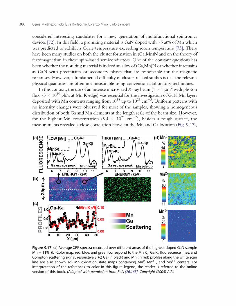
measurements revealed a close correlation between the Mn and Ga location (Fig. 9.17),
Figure 9.17 (a) Average XRF spectra recorded over different areas of the highest doped GaN sampleMn¼ 11%. (b) Color map: red, blue, and green correspond to the Mn Ka, Ga Ka fluorescence lines, andCompton scattering signal, respectively. (c) Ga (in black) and Mn (in red) profiles along the white scanline are also shown. (d) Mn oxidation state maps containing Mn0, Mn2þ, and Mn3þ centers. Forinterpretation of the references to color in this figure legend, the reader is referred to the onlineversion of this book. (Adapted with permission from Refs [76,165]. Copyright (2005) AIP.)
386 Gema Martinez-Criado, Elisa Borfecchia, Lorenzo Mino, Carlo Lamberti

confirming that there is a partial substitution of Ga by Mn [74]. Because the surface atom
diffusion length and the local strain field are both finite, Mn clustering could become
more probable for strongly doped layers.
Moreover, XANES data recorded at the Mn K-edge displayed the dipole-allowed
transitions of photoelectrons fromMn 1s states to unoccupied 4p-like states. Usually, the
large density of unfilled d states from the transition metal do not contribute to a K edge,
but without inversion symmetry mixing of the Mn 3d with N 2p character states from
the surrounding atoms takes place [75], giving rise to the pre-edge peaks. At very high
manganese levels, the reduced amplitude of all oscillations reflected a change in the local
chemical and crystallographic environment around manganese, strongly supporting
doping-induced disorder effects [76].
In the same way, the analysis of Si impurities in molecular beam epitaxy-grown
AlGaN has also been performed with a 2 # 1 mm2 beam size by soft scanning XRM at
the Swiss Light Source by Somogyi et al. [77]. The formation of Si clusters accompanied
with compositional modulation (lower Ga and higher Al concentrations) was observed
within Si-rich precipitates (Fig. 9.18). Detected by micro-XANES in XRF and TEY
modes, the static disorder around the Si atoms increased with the Si content, while the
hexagonal crystal structure was retained. Although phase separation is considered to be
unlikely due to the small lattice mismatch between AlN and GaN, the reported results
indicated its existence in AlGaN.
In summary, scanning micro-XRF shows the cluster formation on the micrometer
scale, while the incorporation of doping-induced defects, which clearly lower the short-
range symmetry, was detected by micro-XANES.
Figure 9.18 XRF images obtained by measuring the AleKa, SieKa and GaeLa fluorescence lineintensities. The H # V pixel size is 5 # 20 mm2 in the larger and 2 # 1 mm2 in the smaller images. Redcolor indicates the high fluorescence intensity, blue color, the low intensity. In addition, the figureshows the Si K-edge XANES spectra measured in spots of different Si concentrations in XRF and TEYmodes. For interpretation of the references to color in this figure legend, the reader is referred to theonline version of this book. (Adapted with permission from Ref. [77]. Copyright (2007) AIP.)
Micro- and Nano-X-ray Beams 387

7.2. Morphological Defects
The growth of defect-free semiconductor layers with a high degree of morphological
control and surface uniformity is still very difficult nowadays. In GaN, for example,
although the most efficient p-type dopant is Mg, the high doping level necessary to
achieve significant hole concentration induces microstructural planar defects [78].
Various pyramidal structures have been reported in GaN films grown by metaleorganic
chemical vapor deposition (MOCVD). Because of the noncentrosymmetric GaN
nature, these microstructures have been identified as Mg-rich pyramidal inversion
domains, resulting from phase segregation effects [79]. So far, the origin is not
completely understood, but it seems that the nucleation occurs at the sample surface,
inducing changes in the stacking sequence from hexagonal to cubic structures or
formation of Mg3N2 precipitates [80]. However, no direct experimental evidence has
been provided to support these mechanisms. Recently, the use of synchrotron radiation
nanoprobe techniques allowed a better understanding of the underlying structural
process of three-dimensional Mg-rich hexagonal pyramids formed in MOCVD-grown
GaN:Mg films [81].
The XRF data, collected with a 120# 140 nm2 hard X-ray probe obtained using the
KB geometry (Section 5.2), are shown in Fig. 9.19, where the presence of elemental
traces of Cr and Fe is revealed. A blueeredeyellow (BRY) plot displays the Ga-, Cr- and
Fe-Ka intensity distributions. While Ga arrangement presents equally spaced and
periodic planes sequentially stacked from the hexagonal base, Cr and Fe impurities
exhibit a close correlation on their spatial locations without the 3D pyramidal shape,
Figure 9.19 (a) Optical micrograph of the Mg-rich hexagonal pyramids in GaN. (b) XRF images: BRY plotdisplaying the Ga-, Cr- and Fe-Ka intensity distributions with their corresponding concentrations in thecolor scales. (c) SEM image of the pyramidal defect. For color version of this figure, the reader is referredto the online version of this book. (Adapted with permission from Ref. [81]. Copyright (2009) AIP.)
388 Gema Martinez-Criado, Elisa Borfecchia, Lorenzo Mino, Carlo Lamberti

suggesting the formation of a possible CreFe-related secondary phase. However, no
evidence for such a phase was observed.
These observations emphasized the underlying diffusion mechanism characterized by
impurity agglomeration effects predominantly on the hexagonal base. It supports the
occurrence of such pyramids by the kinetics of several impurities and not only light
elements like O, C and H that accompanied the Mg incorporation [82]. This observation
is consistent with earlier reports that suggest dopant or impurity segregation responsible
for the defect formation in GaN:Mg [83].
XANES measurements probed inside and outside such pyramids are shown in
Fig. 9.20. Since the XANES spectra depend on the short order around the central
absorbing atom, polarization dependence should be expected under certain symmetries.
Typically, two polytypes exist in GaN: zincblende (cubic, Td) and wurtzite (hexagonal,
C6v). For the cubic GaN, an isotropic material, the XANES spectra should not depend
on the angle of incidence q, whereas for the hexagonal GaN, the XANES data are
expected to depend on q, more specifically, the intensities of the resonances and not their
linewidths and energy positions. The resulting data plotted in Fig. 9.20 do not show
Figure 9.20 (a) Calculated and measured XANES data around the Ga K-edge for perpendicular/parallel incidence on the pyramid center and outside. (b) Calculated and measured XLD recorded atthe Ga K-edge with the beam focused on the pyramid center and outside it. For color version of thisfigure, the reader is referred to the online version of this book. (Adapted with permission from Ref. [81].
Copyright (2009) AIP.)
Micro- and Nano-X-ray Beams 389

a clear superposition of the hexagonal spectrum plus a contribution associated with GaN
having cubic symmetry. From the comparison of the X-ray linear dichroism (XLD),
these findings showed that these pyramidal defects exhibit excellent hexagonal crystal-
lographic orientation. Moreover, there was no remarkable damping effect revealing
a strong influence of the Cr and Fe impurities in any preferential crystallographic
direction.
In summary, three-dimensional Mg-rich hexagonal pyramids in GaN were
investigated by XRF excited using a hard X-ray nanobeam. The observations pro-
vided strong evidence for the diffusion and subsequent segregation of background
impurities on these morphological defects. XANES and XLD collections around Ga
atoms have shown tetrahedral coordination without significant local atomic distortion
inside the hexagonal defects, providing direct evidence for the high short-range
structural order [81].
7.3. Short-Range Order
The local structure around dopants in semiconductors plays a key role in their physical
properties such as phase transitions, dynamical behavior, defect formation and/or phase
segregation effects. In the past years, for instance, room-temperature ferromagnetism
has been reported in dilute magnetic semiconductors, but the formation of metallic
precipitates has been held responsible for such magnetic responses. An alternative
solution to the transition metal has emerged based on a rare-earth element. Although
the magnetic coupling strength of f orbitals should be much weaker than that of
d orbitals, due to the stronger localization of the f electrons, there is one rare-earth
element, gadolinium, which presents both partially filled 4f and 5d orbitals [84]. Thus,
in addition to the ferromagnetism above room temperature, a colossal magnetic
moment of about 4000 mB per Gd atom has been recently observed in 400 nm in Gd-
doped GaN layers [85]. However, there are still controversial results on the ferro-
magnetic mechanism. Some findings suggest either the electric polarization of the
hexagonal GaN or a strong long-range interaction between Gd atoms and certain
defects. Contrary to previous results, ohers studies have attributed to the stabilization of
ferromagnetism to nitrogen or gallium vacancies. According to a recent theoretical
study [86], Ga vacancies are also the most effective source of localized holes necessary
for a strong ferromagnetic ped exchange coupling. Furthermore, several reports
have not detected the formation of any secondary phases in GaN, whereas in Gd-
implanted GaN, the presence of precipitates of Gd3Ga2, GdN, and Gd has been
observed [87].
Using an X-ray beam of 1.5 # 3.5 mm2, the incorporation of Gd on GaN films has
been recently addressed by XANES and scanning XRF techniques [88]. The results
revealed uniform patterns with no intensity changes (<0.02%) at the length scale of the
beam size, showing a homogeneous distribution of Ga and Gd. Whereas impurity
390 Gema Martinez-Criado, Elisa Borfecchia, Lorenzo Mino, Carlo Lamberti

aggregation effects were previously observed in heavily rare-earth-doped GaN, this
report showed no tendency to agglomerate at low Gd levels in Gd-doped GaN films.
For the highest Gd-doped GaN (0.027%), the comparison of XLD of XANES
collected at the Gd L3 and Ga K edges supported the tetrahedral Gd3þ site distri-
butions as shown in Fig. 9.21. The XLD signals reflect directly the anisotropy of the
unoccupied density of states of the 5d and 4p shells of the Gd and Ga atoms in the
hexagonal structure. Simulations performed with FEFF8 code [89] (rescaled for
clarity) exhibited similar results in the figure but with larger amplitudes. In addition,
there was no remarkable damping effect that reveals a strong influence of the Gd in
any preferential crystallographic direction [87]. Moreover, as a function of Gd frac-
tion, EXAFS collections (not shown here) around Ga atoms have exhibited no local
atomic distortion, providing direct evidence for the highly short-range structural
order.
In summary, local structural analysis based on XAS-related techniques revealed Gd
ions in a predominantly trivalent state with tetrahedral coordination, occupying Ga sites
in the wurtzite structure [88]. Although the presence of very small amounts cannot be
completely excluded, within the sensitivity of these experimental techniques, neither
secondary phases nor Ga vacancies were observed [90].
Figure 9.21 XANES and XLD signals recorded at the Gd L3 and Ga K edges from the GaN (0.027% Gd).For color version of this figure, the reader is referred to the online version of this book. (Adapted with
permission from Ref. [88]. Copyright (2008) AIP.)
Micro- and Nano-X-ray Beams 391

7.4. Ion Implantation in Single Nanowires
Doping of semiconductor nanowires by transition-metal ions has attracted significant
attention owing to their potential spintronic applications [91]. Such doping is, however,
difficult to achieve in nanostructures by conventional growth procedures. Alternatively, ion
implantation is a viablemechanism for precisely controlling the number and position of the
dopant atoms using different ion doses and subsequent thermal annealing. In this context,
an exhaustive investigation of the transitionmetal distribution over the lattice and the short
structural order is essential to reveal the complete picture of the implantation process. So
far, most of the studies have reported the average local atomic structure and secondary
phases in ensembles of nanowires by XANES and EXAFS [92]. These chemical and local
structural properties have been historically difficult to characterize at the nanoscale owing
to the X-ray beam instability and the chromaticity of the focusing X-ray optics. However,
such difficulties have been recently precluded using a pair of KB Simirrors developed at the
ESRF. In 2011, Segura-Ruiz et al. [93] have used a 100 # 100 nm2 monochromatic hard
X-ray beam to examine the short-range order in single Co-implanted ZnO nanowires. In
addition, the linear polarization of the synchrotron nanobeam made the study capable of
detecting preferentially oriented defects induced by the ion implantation process.
Figure 9.22 shows the SEM image of a single Co-doped ZnO nanowire, indicating
the areas where XANES and EXAFS spectra were recorded (1, 2 and 3). The elemental
Figure 9.22 (a) SEM image of a single Co-implanted nanowire. (b) Elemental map collected at 12 keVfor Co with the respective atomic fraction estimated from the XRF quantification. Zn K edge XANESspectra recorded along the nanowire: (c) with the c-axis oriented perpendicular, and (d) parallel to theelectric field vector of the X-ray nanobeam. For color version of this figure, the reader is referred to theonline version of this book. (Adapted with permission from Ref. [93]. Copyright (2011) ACS.)
392 Gema Martinez-Criado, Elisa Borfecchia, Lorenzo Mino, Carlo Lamberti

map of Co with the respective concentration estimated from the XRF quantification is
displayed in Fig. 9.22b, showing homogeneous distributions of Co along the nanowire
without any signature of clusters or nanoaggregates. XANES data from the nanowire
with its c-axis oriented perpendicular and parallel to the polarization vector of the X-ray
beam are shown in Fig. 9.22c and d, respectively. The spectra exhibit the peaks associated
to the hexagonal structure, without any evidence of lattice damage in the nanowire.
The chemical state of the implanted Co ions was investigated by nano-XANES.
Figure 9.23a shows the XANES spectra around the Zn K edge (solid circles) and Co K
edge (open circles) taken at points 1 and 2. Despite the low Co content, the quality of
the XANES data around the Co K edge is good and reproduces well the oscillations of
the Zn K-edge spectra at both points, suggesting Co ions incorporated into the
wurtzite host lattice on the Zn sites. Furthermore, the good match between the
XANES spectra of the nanowire and that of a high-quality wurtzite Zn0.9Co0.1O
epitaxial film [94] (not shown) suggests oxidation state of 2þ for implanted Co ions.
Finally, nano-EXAFS measurements around the Zn K-edge allow us to study the local
order of the host lattice. Figure 9.23b shows the magnitude of the Fourier transforms of
the EXAFS functions. The spectra show two dominant peaks related to the first O- and
second Zn-shells. In general, there is no evidence of amorphization, and the ZneO
and ZneZn spacings remain equal to those of pure ZnO (1.98 and 3.25 A) along the
nanowire. This confirms the good recovery of the radiation-damaged ZnO lattice
through the thermal annealing.
In summary, an XAS study was carried out in different regions along single nano-
wires. This investigation revealed implanted ions incorporated homogeneously along the
nanowire as Co2þ and occupied Zn sites into the host lattice. The radiation damage in
the ZnO host lattice was completely recovered through thermal annealing [93].
Figure 9.23 (a) XANES spectra around the Zn K edge (solid circles) and Co K edge (open circles) takenat points 1 and 2. For comparison between Zn and Co XANES spectra, the energy has been rescaled tothe respective absorption K edges calculated from the first derivative of the XANES signal.(b) Magnitude of the Fourier transforms of the EXAFS functions (open symbols) and their best fits(solid lines). For color version of this figure, the reader is referred to the online version of this book.(Adapted with permission from Ref. [93]. Copyright (2011) ACS.)
Micro- and Nano-X-ray Beams 393

7.5. Breakdown Sites in Photovoltaic Materials
Diode breakdown in multicrystalline silicon solar cells has become an increasingly
important issue in recent years. The development of new feedstock fabrication sources,
which provide cheaper but at the same time also dirtier silicon, has forced cell module
manufacturers to adapt the module design to inferior breakdown behavior of the resulting
solar cells. Recently, at least three different breakdownmechanisms have been identified in
mc-Si solar cells [95,96]. One of them is related to recombination centers in the Si crystal,
often related to dislocations and grain boundaries. The breakdown voltage has been found
to be directly correlated with the impurity concentration of the silicon wafer. The higher
the transition metal concentration in the wafer, the lower the breakdown voltage. Thus,
the important question is whether the transition metals directly lead to prebreakdown or
whether secondary effects like dislocation multiplication due to strain fields in the Si
crystal result in decreased breakdown voltage. m-XRF is the ideal tool to answer this
question since no sample preparation (e.g. for transmission electron microscope (TEM)-
based investigations), which possibly alters the sample properties, is necessary.
Kwapil et al. examined a solar cell from the bottom of the ingot using a nano X-ray
beam [97]. The local prebreakdown behavior was preliminarily characterized by bias-
dependent electroluminescence intensity measurements. A sample of 10 # 20 mm2
featuring a high density of prebreakdown sites which were related to recombination
active defects was cut out. Then, microscopic investigations were carried out with an
electro-/photoluminescence-spectroscopy mapping tool with a spatial resolution in the
order of 1 mm. In Fig. 9.24, the SEM image of a small grain is shown. By applying 10 V
(a) (b)
Figure 9.24 The image reported in panel (a) is a part of the solar cell, which shows recombinationactive features in dark. Except for the straight black lines running from left to right, they belong to thesolar cell and are situated at the surface of the silicon wafer. In panel (b), an SEM image of the part ofthe solar cell marked by the dotted rectangle in panel (a) is repored, as well as the m-XRF maps ofmetal Fe precipitates labeled as 1 and 2 in the SEM micrograph and highlighted by with circles. Forcolor version of this figure, the reader is referred to the online version of this book. (Adapted with
permission from Ref. [97]. Copyright (2009) AIP.)
394 Gema Martinez-Criado, Elisa Borfecchia, Lorenzo Mino, Carlo Lamberti
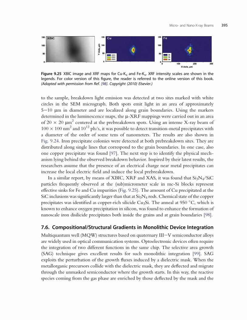
to the sample, breakdown light emission was detected at two sites marked with white
circles in the SEM micrograph. Both spots emit light in an area of approximately
5e10 mm in diameter and are localized along grain boundaries. Using the markers
determined in the luminescence maps, the m-XRF mappings were carried out in an area
of 20 # 20 mm2 centered at the prebreakdown spots. Using an intense X-ray beam of
100# 100 nm2 and 1012 ph/s, it was possible to detect transition-metal precipitates with
a diameter of the order of some tens of nanometers. The results are also shown in
Fig. 9.24. Iron precipitate colonies were detected at both prebreakdown sites. They are
distributed along single lines that correspond to the grain boundaries. In one case, also
one copper precipitate was found [97]. The next step is to identify the physical mech-
anism lying behind the observed breakdown behavior. Inspired by their latest results, the
researchers assume that the presence of an electrical charge near metal precipitates can
increase the local electric field and induce the local prebreakdown.
In a similar report, by means of XBIC, XRF and XAS, it was found that Si3N4/SiC
particles frequently observed at the (sub)micrometer scale in mc-Si blocks represent
effective sinks for Fe and Cu impurities (Fig. 9.25). The amount of Cu precipitated at the
SiC inclusions was significantly larger than that at Si3N4 rods. Chemical state of the copper
precipitates was identified as copper-rich silicide Cu3Si. The anneal at 950(C, which is
known to enhance oxygen precipitation in silicon, was found to enhance the formation of
nanoscale iron disilicide precipitates both inside the grains and at grain boundaries [98].
7.6. Compositional/Structural Gradients in Monolithic Device Integration
Multiquantum well (MQW) structures based on quaternary IIIeV semiconductor alloys
are widely used in optical communication systems. Optoelectronic devices often require
the integration of two different functions in the same chip. The selective area growth
(SAG) technique gives excellent results for such monolithic integration [99]. SAG
exploits the perturbation of the growth fluxes induced by a dielectric mask. When the
metallorganic precursors collide with the dielectric mask, they are deflected and migrate
through the unmasked semiconductor where the growth starts. In this way, the reactive
species coming from the gas phase are enriched by those deflected by the mask and the
Figure 9.25 XBIC image and XRF maps for Cu-Ka and Fe-Ka. XRF intensity scales are shown in thelegends. For color version of this figure, the reader is referred to the online version of this book.(Adapted with permission from Ref. [98]. Copyright (2010) Elsevier.)
Micro- and Nano-X-ray Beams 395
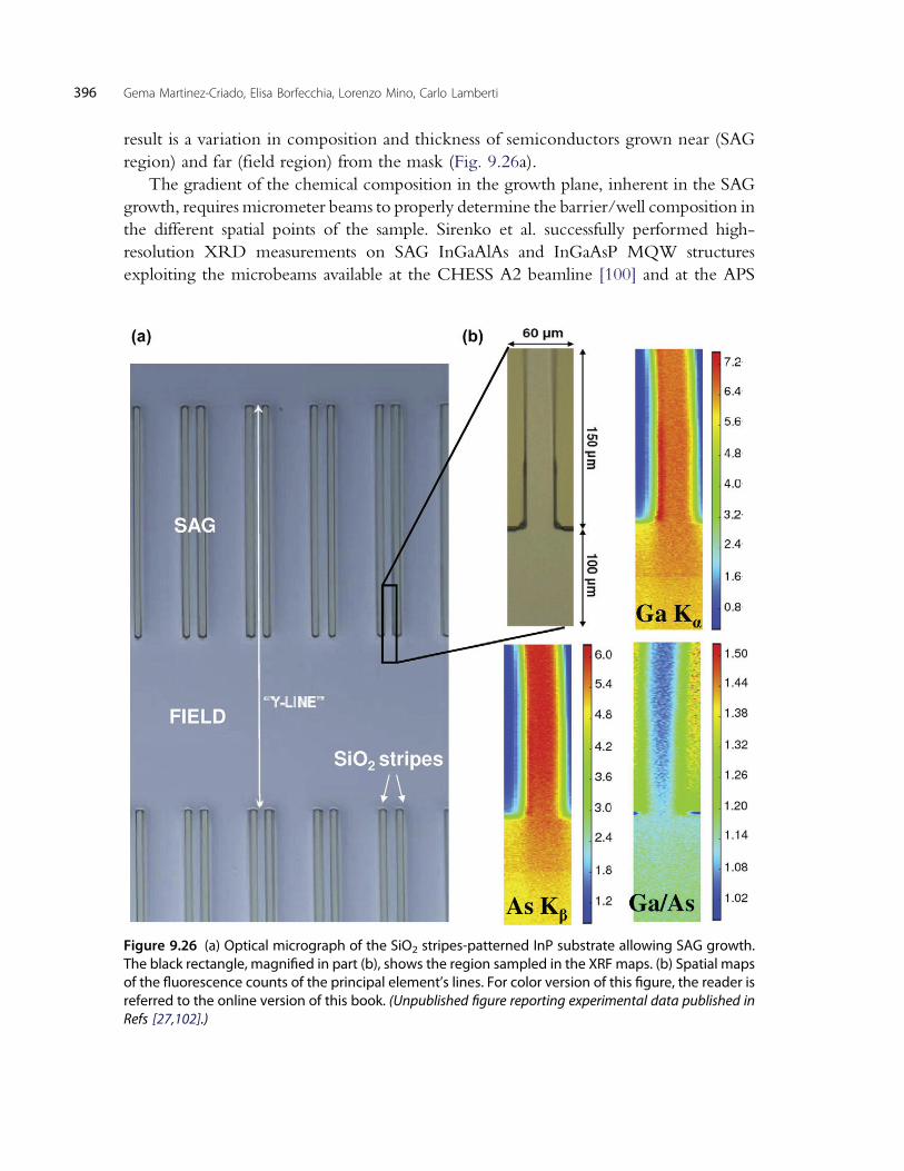
result is a variation in composition and thickness of semiconductors grown near (SAG
region) and far (field region) from the mask (Fig. 9.26a).
The gradient of the chemical composition in the growth plane, inherent in the SAG
growth, requires micrometer beams to properly determine the barrier/well composition in
the different spatial points of the sample. Sirenko et al. successfully performed high-
resolution XRD measurements on SAG InGaAlAs and InGaAsP MQW structures
exploiting the microbeams available at the CHESS A2 beamline [100] and at the APS
Figure 9.26 (a) Optical micrograph of the SiO2 stripes-patterned InP substrate allowing SAG growth.The black rectangle, magnified in part (b), shows the region sampled in the XRF maps. (b) Spatial mapsof the fluorescence counts of the principal element’s lines. For color version of this figure, the reader isreferred to the online version of this book. (Unpublished figure reporting experimental data published in
Refs [27,102].)
396 Gema Martinez-Criado, Elisa Borfecchia, Lorenzo Mino, Carlo Lamberti

2-ID-D microscope beamline [101]. The electroabsorption modulated laser (EML),
obtained by monolithic integration of an EAM with a distributed feedback laser (DFB), is
one of the most promising applications of SAG. A voltage modulation applied to the
electroabsorption modulated (EAM) switches it between an opaque and a transparent state
bymeans of the Stark effect and ensures themodulation of theDFB laser emission, allowing
long-distance communication at high frequency. Recently, Mino et al. characterized an
SAG EML device of industrial interest based on an AlxwGaywIn1exweywAs/AlxbGaybIn1exbeybAs (compressive-strained well/tensile-strained barrier) MQW structure grown
on InP by metallorganic vapor phase epitaxy. The mask used for the growth (Fig. 9.26a)
featured 20-mm-wide SiO2 stripes with a 30 mm opening width between them [102].
The XRF maps (Fig. 9.26b) reveal that Ga Ka and As Kb counts are higher in the
SAG region owing to material enrichment caused by the SiO2 stripes. The effectiveness
of the SAG technique in modulating the chemical composition of the quaternary alloy is
proven by the map reporting the ratio between Ga and As counts, in which a gradient in
the average well/barrier chemical composition is clearly visible. Since the Ga/As ratio is
lower in the SAG region than in the field, it is shown that the average Ga content of the
MQW structure progressively increases by moving from the SAG to the field (along the
Y-line showed in Fig. 9.26a).
The structural parameters of the sample were investigated by micro-XRD: 35
different spatial points were sampled along the Y-line (Fig. 9.27a). With such data, it is
possible to obtain the widths (wb, ww, Fig. 9.27c) and the mismatches (mb, mw, Fig. 9.27d)
of the barrier and of the well by fitting the experimental patterns (Fig. 9.27b) [103]. Both
wb and ww undergo a modulated increase moving from field to SAG regions: this is the
direct measure of the material enrichment in the SAG region. Moreover, both mb and
mw values increase almost monotonically moving from the field to the SAG reflecting the
expected modulation of the AlxGayIn1!x!yAs composition of barrier and well layers.
This key information, coupled with the micrometer determination of the energy gap
by photoluminescence, led to a characterization of the structural gradient of the MQW
structure along the Y-line from the field to the SAG region.
In summary, the composition and the structure of the SAG EML device were
determined with a spatial resolution of 2 mm, thus giving the appropriate feedback
needed to improve the growth process, previously based only on a trial-and-error
approach This characterization approach was also extended to other SAG growths with
different stripes and opening sizes [27,104,105].
7.7. Scanning X-Ray Diffraction Imaging of Individual SiGe/Si Islands
Chemical composition and strain distribution are two key parameters influencing many
structural and electronic properties of semiconductor micro- and nanostructures. With
the development of increasingly miniaturized structures for technological applications in
electronics and photonics, the use of local probes is becoming more and more relevant to
Micro- and Nano-X-ray Beams 397
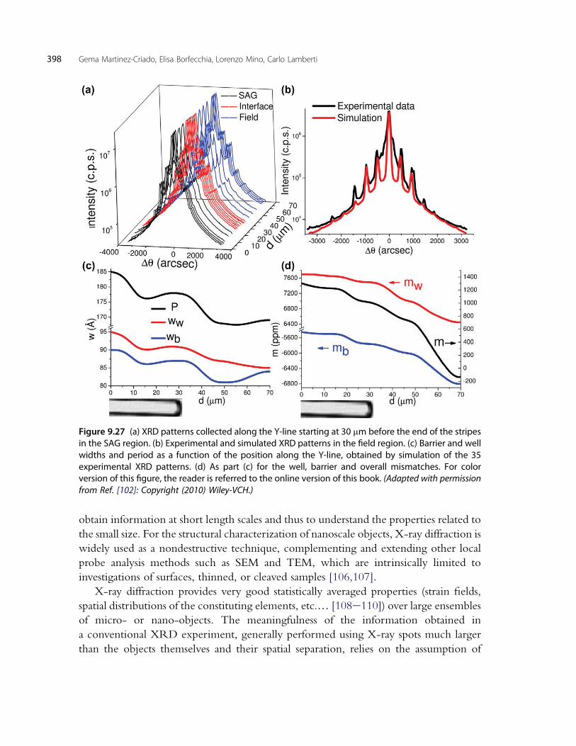
obtain information at short length scales and thus to understand the properties related to
the small size. For the structural characterization of nanoscale objects, X-ray diffraction is
widely used as a nondestructive technique, complementing and extending other local
probe analysis methods such as SEM and TEM, which are intrinsically limited to
investigations of surfaces, thinned, or cleaved samples [106,107].
X-ray diffraction provides very good statistically averaged properties (strain fields,
spatial distributions of the constituting elements, etc.. [108e110]) over large ensembles
of micro- or nano-objects. The meaningfulness of the information obtained in
a conventional XRD experiment, generally performed using X-ray spots much larger
than the objects themselves and their spatial separation, relies on the assumption of
Figure 9.27 (a) XRD patterns collected along the Y-line starting at 30 mm before the end of the stripesin the SAG region. (b) Experimental and simulated XRD patterns in the field region. (c) Barrier and wellwidths and period as a function of the position along the Y-line, obtained by simulation of the 35experimental XRD patterns. (d) As part (c) for the well, barrier and overall mismatches. For colorversion of this figure, the reader is referred to the online version of this book. (Adapted with permission
from Ref. [102]: Copyright (2010) Wiley-VCH.)
398 Gema Martinez-Criado, Elisa Borfecchia, Lorenzo Mino, Carlo Lamberti
a small dispersion in the properties of many individual structures. In many cases,
however, it is desirable to combine different analysis techniques on exactly the same
object belonging to a larger ensemble, for instance, to achieve a more detailed insight
into the interdependence of properties. Focused X-ray beams with diameters down
to the submicron range, which are available at third-generation synchrotron sources,
offer unique possibilities for micro- or even nano-XRD studies of individual low-
dimensionality structures.
SiGe/Si(001) islands grown by liquid-phase epitaxy represent an ideal model system
to test the capabilities of such local use of XRD technique. In fact, depending on the
applied Ge content, one can accurately adjust the final island size in the range of
3 mme50 nm [111]. By also varying the growth time, subsequent growth stages with
well-defined morphologies can be obtained, e.g. flat islands with side facets less steep
than (111) or complete objects, consisting in square-based truncated pyramids with (111)
side facets and (001) top facets [112]. Compositional, structural and elastic features of
such structures have been therefore extensively investigated, manly at micro-XRD
beamlines ID01 and ID13 of the ESRF [113e118]. Generally, the X-ray reciprocal space
mapping (RSM) method [109] has been employed. This approach provided detailed
information on strain and composition in self-organized islands systems when coupled
with simulations based on finite element methods (FEM) [119] for lattice displacements
determination.
Mocuta et al., for instance, investigated several samples with island sizes between
200 nm and 3.2 mm employing a 5 # 3 mm2 X-ray beam at beamline ID01 (ESRF)
[113]. Recording the intensity of the SiGe (004) reflection as a function of the X-ray
micro-beam position on the sample, a map of the islands position was recorded (scanning
X-ray diffraction, SXD imaging, see Fig. 9.28a). This approach thus combines a high
resolution in reciprocal space, measuring in details of the intensity distribution around
a Bragg peak, with a micrometer spatial resolution in real space [110].
In Fig. 9.28b, RSM data obtained for SiGe islands around (004) reciprocal lattice
point are reported as an example. Left panel shows RSM resulting from ensemble average
over ca 103 islands, while middle and right panels report intensity distributions found in
the case of two individual islands at different stages of the growth process, labeled as IL1
(fully developed truncated pyramid) and IL2 (flat island), see also SEM images in top
insets.
From model fitting, the Ge distribution as well as the strain distribution was obtained
[113]. For the fully developed IL1, the FEM-based simulations indicated a step in Ge
content at 1/3 of the island height. On the contrary, in the case of the flat island IL2, the
best agreement with RSM data was found assuming the 2/3 top part as missing, therefore
demonstrating that this island represents an intermediate growth stage. It is worth
noticing that the identification of flat islands as intermediate grow stages and their
structural characterization can be uniquely obtained using high-brilliance synchrotron
Micro- and Nano-X-ray Beams 399

microbeams for local SXD imaging and characterization. This kind of islands, in fact,
represents only a very small fraction of the total (about 2e4%, comprising only about 1%
of the scattering volume): their contribution to the total scattering in an ensemble-
averaging experiment is therefore completely negligible.
The spot size of 5# 3 mm2 employed by Mocuta et al. in the study hitherto discussed
did not allow spatial discrimination of possible substructures within the single island
investigated. A further improvement in terms of spatial resolution was obtained
by Hanke et al., at the beamline ID13 of the ESRF [114]. Using a set of refractive
silicon X-ray lenses (see Section 5.1) to focus the X-ray beam size down to a diameter
of 200 nm FWHM, detailed SXD scans inside individual micrometer-sized and even
smaller islands were enabled. By illuminating diverse (111) island side facets, crystal
truncation rods of different orientations were independently excited and thus became
distinguishable in the scattering patterns, as can be observed in Fig. 9.28c. An analog
experiment was reported by Diaz et al. [115], implementing an acquisition method that
does not required the recording of the whole 3D reciprocal space at each position in
real space, thus reducing instability problems during the measurements. Several
Figure 9.28 (a) Diffracted intensity as a function of lateral sample position with the angles tuned to the(004) Bragg peak of relaxed SiGe; an optical microscopy image of the region of the SXD map high-lighted in the dotted box is shown for comparison. In the inset, a schematics of the method is reported:elastic scattering from the spot illuminated by a microfocused X-ray beam is detected (ki and kf are thescattering vectors); when the X-ray spot illuminates a single island, a broad signal due to lattice spacingdistribution inside the SiGe islands is observed, in addition to the sharp peak related to the substrate.(b) Reciprocal space mapping (RSM) of SiGe islands around (004) peak; left panel: results from ensembleaverage over ca 103 islands (numerical labels 1e4) indicate the following relevant features: 1, lineardetector saturation streak; 2, monochromator streak; 3, Si surface crystal truncation rod (CTR), 4, facetstreaks originating from the (111) island side facets. Right panels: RSM from two individual islands IL1(fully developed truncated pyramid) and IL2 (flat island), see also SEM images in upper insets. (c) Toppanels: 3 # 3 mm2 SEMmicrograph of a single SiGe island and corresponding SXD map obtained usingthe diffusely scattered X-ray intensity in proximity of the symmetric Si (004) reflection. Bottom panel:reassembled diffraction pattern of a single island, obtained using frames 12e14 of the SXD map. Forcolor version of this figure, the reader is referred to the online version of this book. (Adapted with
permission from Ref. [113]: Copyright (2008) APS, and Ref. [114]: Copyright (2008) AIP.)
400 Gema Martinez-Criado, Elisa Borfecchia, Lorenzo Mino, Carlo Lamberti

advanced studies on the same and analog systems have been subsequently performed.
For instance, SiGe islands elastic properties were probed in situ by combining atomic
force microscopy (AFM) and micro-XRD on a single nanostructure [116,117]. In
addition, Dubslaff et al. investigated by scanning X-ray nanodiffraction individual self-
assembled SiGe/Si(001) dot molecules, containing either one, two, three, or four dots,
using a beam size of 250 nm [118]. Recently, the nanobeam setup available at beamline
ID01 of the ESRF was exploited for a challenging study that perfectly demonstrates the
state-of-art capabilities of synchrotron-based nano-XRD methods. In such work,
Hrauda et al. determined the strain fieldselds in and around a single SiGe island, which
serves as stressor for the Si-channel in a fully functioning metal-oxide-semiconductor
field-effect transistor (MOSFET) [120]. The authors found tensile strain values up to
1% along the source-drain direction in the MOSFET Si channel above the SiGe stressor
dot, using RSM- and FEM-based simulations (see Fig. 9.29 and relative caption for
further details).
7.8. Local Structure of Single Semiconductor Rolled-Up Nanotubes
Rolled-up nano(micro)tubes (RUN(M)Ts) [121,122] are unique structures, consti-
tuted by a crystalline layer which is oriented in all azimuthal directions, thus exhibiting
a nearly perfect cylindrical symmetry. These objects can be obtained by rolling up
a highly strained single-crystalline multilayer. After a partial release from a substrate by
selective underetching, the free multilayer relaxes the strain elastically by rolling up
(a) (b) (c)
Figure 9.29 (a) SEM micrographs of the MOSFET device at different magnifications (top panels),compared with images obtained in SDX mode at the same scale (bottom panels, left panel:diffractometer tuned to Si (004) peak to find the transistor junction; middle and right panels:diffractometer tuned to SiGe (224) signal to locate the dot islands). (b) RSM around (224) Braggpeak measured on the SiGe dot buried under the transistor gate; the map includes the Si (224)bulk peak and the SiGe (224) dot signal in its lower left section (highlighted by the dashed circle).(c) Top panel: FEM-based simulated data, calculated for the region around the diffuse SiGe (224)signal, delimited by the orange box in part (b); bottom panels: resulting 2D maps of the Geconcentration and the in-plane strain εxx. For interpretation of the references to color in thisfigure legend, the reader is referred to the online version of this book. (Adapted with permission
from Ref. [120]: Copyright (2011) ACS.)
Micro- and Nano-X-ray Beams 401

into a well-positioned micro/nanotube, the radius of which is influenced by multilayer
thickness and elastic properties [123]. In the case of semiconductor materials
[121,122,124e126], these structures are characterized by a very good crystalline
quality and a wall thickness of several atomic monolayers, showing several analogies
with their carbon-based counterpart. Semiconductor RUNTs are therefore very
promising candidates for the use as integrative components such as 2D confined
channels for fluid filling and transport [127], coils, transformers, capacitors [124], or
optical waveguides [125]. In addition, RUMT containing light emitters have been
employed as optical ring resonators [128e130] for optoelectronics [131], with emis-
sion energy depending on tube local curvature and strain state of both the RUMTand
the integrated emitter [132].
In order to fully understand RUNTs growth process and resulting mechanical and
electronic properties of the tubes, and to optimize their design toward technological
applications, it is essential to deeply characterize their local structure and final strain state.
A detailed knowledge of local strain distribution is crucial, in particular, for bandgap
engineering applications to the optoelectronic field. Both TEM [133e135] and micro-
Raman spectroscopy [133,134] were employed for this aim, demonstrating that the
nanotubes consist of radial superlattices with alternating crystalline and noncrystalline
layers [133]. However, both the techniques were unable to probe the crystalline interface
within the multilayer and required the separation of the RUNT from the substrate,
thereby possibly modifying its structure. The ideal alternative is XRD, able to
provide very detailed insights on semiconductor thin-film local structure and strain
distribution, in a nondestructive way [136]. As introduced in the previous section, from
standard XRD analysis, statistically averaged information over the illuminated ensemble
of micro/nano-objects is obtained (assuming a typical beam diameter in the 0.1 mm to
few millimeter range, from 104 to 107 individual structures are simultaneously probed
[110]). Conversely, using X-ray microbeams available at synchrotron facilities, an indi-
vidual RUNT can be selected and characterized, exploring in detail its local structural
features at the crystalline interface.
Krause et al. studied the local structure and, in particular, the lattice parameter
distribution of GaAs/InGaAs RUNTs connected to a GaAs(001) substrate using such
approach [137]. The authors employed the microprobe setup available at the beamline
ID01 of the ESRF, where a 10 keV X-ray beam with a spot of 6 # 6 mm2 was obtained
with a circular FZP (Section 5.3.1). Three different pseudomorphic GaAseInGaAs
bilayers were grown, varying the thickness of the GaAs layer (see Fig. 9.30a for SEM
micrographs of the three resulting RUNTs).
The individual RUNT selected for structural characterization was located using
a combination of both optical alignment and XRD scans (see Fig. 9.30b and relative
caption for details). The XRD signal observed for all the three analyzed RUNTs shows
two characteristic well-separated Bragg peaks, clearly distinguishable from the
402 Gema Martinez-Criado, Elisa Borfecchia, Lorenzo Mino, Carlo Lamberti

monotonously increasing background, as reported in Fig. 9.30c. The peak at ca 4.45 A!1
well fits the bulk GaAs position, while the other, found at ca 4.35 A!1, falls between the
strained InGaAs position and the position expected after complete InGaAs relaxation,
from Vegard’s law.
The presence of two distinct peaks demonstrated that the crystalline bilayer is
maintained also in the RUNTs, while the intermediate position of the peak assigned to
InGaAs indicated only a partial relaxation of the individual layers, due to a mutual
torsional moment. The lattice parameter distributions of the RUNTs were calculated by
minimization of the total elastic energy, following Grundmann [138] (Fig. 9.30d);
Figure 9.30 (a) SEM images of the three RUNTs investigated by Krause et al. using micro-XRD,characterized by three different thickness of the GaAs layer. (b) Correlation of an optical microscopyimage with the X-ray measurements for determination of the tube position: the selected tube isoptically pre-aligned with its axis perpendicular to the incoming X-ray beam. Because of the rolling-up,the crystalline lattice of the tube is oriented isotropically perpendicular to the tube axis, and theisotropic scattering intensity in azimuthal direction is independent of a (geometry (1) in Figure 9.30b).By detuning the incident angle (geometry (2) in Figure 9.30b), the thermal diffuse backgroundscattering of the substrate can be sufficiently reduced, so that the scattering of the RUNTs isdiscriminated from the background signal. (c) Intensity distribution, normalized to the GaAs reflection,for RUNT (I)-(III). The experimental data are shown as black dots, the simulations as red lines. (d) Latticeparameter distribution at in tangential direction (filled circles) and ar in radial direction (open circles)as used for the simulations. For interpretation of the references to color in this figure legend, thereader is referred to the online version of this book. (Adapted with permission from Ref. [137]. Copyright
(2006) APS.)
Micro- and Nano-X-ray Beams 403

subsequently, the X-ray scattered intensity was simulated in kinematic approximation
from the lattice parameter distribution (red solid curves in Fig. 9.30c), obtaining a very
good agreement with experimental data.
The study hitherto discussed laid the foundations of a more comprehensive
investigation by the same research group. In this later work, Malachias et al. [139]
proposed a detailed comparison of the strain status in different semiconductor RUNTs
(bilayers, multilayers and layers with dislocations), selected to evidence the influence
of different layer configuration on lattice relaxation. The local structural character-
ization was performed using synchrotron micro-XRD, with a setup analogous to that
previously described, and continuum elasticity theory to model and interpret the
experimental data. More recently, the same microprobe setup was employed to
investigate the shift in optical response of an AlGaAs/GaAs quantum well integrated
in the wall of RUMT, as a function of the position along the tube axis [140]. Micro-
XRD scans using a 6 # 5 mm2 X-ray beam provided local insights in the rolled-up
heterostructure strain state, and were combined with 10 K PL measurements probing
the optical response when moving along the same RUMT, with 1 # 1 mm2 resolution.
Combined analysis of PL and XRD data demonstrated that the investigated optically
active RUMT shows different strain states on different windings at the same lateral
position [140].
In conclusion, the presented cases evidence the potential of X-ray microbeam
diffraction as a nondestructive probe to study the local structure of individual rolled-up
semiconductor nano/microtubes, overcoming the limit of incoherent statistical aver-
aging affecting standard XRD analysis. This technique promises to be extremely useful
for the structural characterization of rolled-up crystalline layers of various compositions,
thicknesses, and sizes, thus helping to understand their fundamental functional properties
in future integrated devices.
7.9. Local Strain Characterization in Microelectronic Materialsand Devices
The microelectronic industry is continuously searching for technological solutions to
further improve performances and speed of Si-based integrated devices as MOSFETs
and complementary metal-oxide semiconductor (CMOS) transistors. A key method,
constituting a valid alternative to the traditional downscaling of device dimensions, relies
on the controlled application of strain distribution to current-carrying regions of the
transistor, tailored to improve the carrier mobility. As first illustrated by Bardeen and
Shockley (1950) and subsequently quantified by Smith (1954), the local strain applied to
semiconductor crystal layers in fact directly influences the material resistivity as well as
the carrier mobility.
Several methods have been consequently employed to induce that local strain in the
channel of MOS-based devices. A common strategy consists in the deposition of
404 Gema Martinez-Criado, Elisa Borfecchia, Lorenzo Mino, Carlo Lamberti

embedded heteroepitaxial structures into Si trenches [141,142]. The most frequently
used materials for stressor structures are SiGe [143], with lattice spacing larger than Si,
thus inducing a compressive strain on the channel and SiC, which conversely causes
a tensile in-plane strain, due to its shorter lattice parameter. An alternative approach is
the growth of stressed thin films (e.g. Si3N4) overlying the transistor. In such case, the
edges of the gate region induce local stress concentrations on the source-drain
Si channel, resulting in an in-plane strain distribution with the same sign of the over-
laying film [144].
Both the procedures mentioned above result in heterogeneous strain distribution
within the current-carrying channel. The use of a simplified model based only on
electrical parameters and assuming a uniform stress along the channel can lead to severe
errors and is definitely inadequate to provide reliable previsions for device performances.
Direct experimental determination of the local strain state across the current-carrying
paths within the device is therefore crucial although challenging under several aspects.
TEM-based techniques (e.g. convergent beam electron diffraction) have an
outstanding spatial resolution [145,146], but a relevant sample preparation is required,
that unavoidably modifies the original strain state of the device in its operational
condition. Micro-Raman spectroscopy is a suitable alternative to obtain information on
local strain at submicrometric scale [147], but the strain tensor dimensionality has to be
assumed a priori, and a calibration procedure is required. In addition, the laser-induced
heating of the sample can bias the results, as reported in particular for the case of
silicon-on-insulator (SOI) layers [148].
Direct insights in local strain distribution can instead be obtained nondestructively
with submicrometric space-resolution by performing XRD measurements with highly
focused X-ray beams available at third-generation synchrotron facilities. This research
branch has been extensively developed at microdiffraction beamline 2-ID-D [149] of the
advanced photon source [150e155] and at the X20A beamline [156] of Brookhaven
National Laboratory’s National Synchrotron Light Source [157,158].
The earlier studies reported by Mooney et al. [157] and later by Eastman et al. [150]
exploited the X-ray microbeams capabilities to investigate microstructural features in
Si1!xGex/Si(001) epitaxial layers, with application in high-speed FETs as buffer layer on
which strained Si or Si1!xGex carrier channels can be pseudomorphically grown
[159e162]. For instance, high angular resolution rocking curves acquired as a function
of the position on the layer using an 8.05 keV microbeam allowed the detection of indi-
vidual tilted rectangular columnar micrograins in step-graded Si1!xGex/Si epilayers [150].In the following decade, several studies were reported focusing on experimental
determination of local strain distribution in situ within the final device, characterized via
microdiffraction in its fully operational state. The effect of both overlying thin films
features [151,158,163,164] and embedded stressor structures [152,153,155,163] on the
resulting FET channel strain was investigated.
Micro- and Nano-X-ray Beams 405
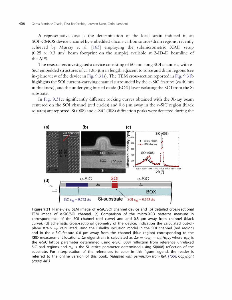
A representative case is the determination of the local strain induced in an
SOI-CMOS device channel by embedded silicon-carbon source/drain regions, recently
achieved by Murray et al. [163] employing the submicrometric XRD setup
(0.25 # 0.3 mm2 beam footprint on the sample) available at 2-ID-D beamline of
the APS.
The researchers investigated a device consisting of 60-nm-long SOI channels, with e-
SiC embedded structures of ca 1.85 mm in length adjacent to sorce and drain regions (see
in-plane view of the device in Fig. 9.31a). The TEM cross-section reported in Fig. 9.31b
highlights the SOI current-carrying channel surrounded by the e-SiC features (ca 40 nm
in thickness), and the underlying buried oxide (BOX) layer isolating the SOI from the Si
substrate.
In Fig. 9.31c, significantly different rocking curves obtained with the X-ray beam
centered on the SOI channel (red circles) and 0.8 mm away in the e-SiC region (black
squares) are reported. Si (008) and e-SiC (008) diffraction peaks were detected during the
(a) (b) (c)
(d)
Figure 9.31 Plane-view SEM image of e-SiC/SOI channel device and (b) detailed cross-sectionalTEM image of e-SiC/SOI channel. (c) Comparison of the micro-XRD patterns measure incorrespondence of the SOI channel (red curve) and and 0.8 mm away from channel (blackcurve). (d) Schematic cross-sectional geometry of the device, indication the calculated out-of-plane strain ε33 calculated using the Eshelby inclusion model in the SOI channel (red region)and in the e-SiC feature 0.8 mm away from the channel (blue region) corresponding to theXRD measurement locations. Dε eigenstrain is calculated as Dε ¼ (aSiC ! aSi)/aSiC, where aSiC isthe e-SiC lattice parameter determined using e-SiC (008) reflection from reference unrelaxedSiC pad regions and aSi is the Si lattice parameter determined using Si(008) reflection of thesubstrate. For interpretation of the references to color in this figure legend, the reader isreferred to the online version of this book. (Adapted with permission from Ref. [155]: Copyright
(2009) AIP.)
406 Gema Martinez-Criado, Elisa Borfecchia, Lorenzo Mino, Carlo Lamberti
same q/2q scan, with the X-ray beam intercepting both types of layers. The measured
out-of-plane strains in the e-SiC region, calculated from diffraction data reported in
Fig. 9.31c, are 0.355% within the vicinity of the channel and 0.350% 0.8 mm away from
the channel, in good agreement with the values predicted by an Eshelby inclusion
model (see Fig. 9.31d and relative caption). Moreover, comparing the two Si(008)
diffraction peaks measured in correspondence of the SOI channel and at 0.8 mm distance,
the authors succeeded in extracting the depth-averaged strain information from the
current-carrying path, resulting in an out-of-plane compressive strain of !0.167%,approximately 95% of the theoretically predicted value.
8. SUMMARY AND FUTURE PERSPECTIVES
Although the optical quality of the X-ray focusing devices has limited the progress of
XRM, recent advances in fabrication techniques as well as in theoretical approaches have
pushed the spatial resolution toward the diffraction limit. As a result, the semiconductor
research using nano- and micro-X-ray beams has begun to extend toward the atomic
domain with the exploitation of size and quantum confinement effects in nanowires, or
self-assembly and patterning at the nanoscale. In addition, the concomitant and
continuous developments of multiple analytical tools in parallel with sophisticated
environments have initiated the full characterization of diluted heterogeneous semi-
conductors in operation at the nanometer scale.
REFERENCES
[1] G.E. Ice, J.D. Budai, J.W.L. Pang, Science 334 (2011) 1234.[2] H. Mimura, S. Handa, T. Kimura, H. Yumoto, D. Yamakawa, H. Yokoyama, S. Matsuyama, K. Inagaki,
K. Yamamura, Y. Sano, K. Tamasaku, Y. Nishino, M. Yabashi, T. Ishikawa, K. Yamauchi, Nat. Phys. 6(2010) 122.
[3] D.H. Bilderback, P. Elleaume, E. Weckert, J. Phys. B At. Mol. Opt. Phys. 38 (2005) S773.[4] S.M. Gruner, AIP Conf. Proc. 1234 (2010) 69.[5] J. Vila-Comamala, S. Gorelick, E. Farm, C.M. Kewish, A. Diaz, R. Barrett, V.A. Guzenko,
M. Ritala, C. David, Opt. Express 19 (2011) 175.[6] K. Evans-Lutterodt, A. Stein, J.M. Ablett, N. Bozovic, A. Taylor, D.M. Tennant, Phys. Rev. Lett. 99
(2007) 134801.[7] K. Yamauchi, H. Mimura, T. Kimura, H. Yumoto, S. Handa, S. Matsuyama, K. Arima, Y. Sano,
K. Yamamura, K. Inagaki, H. Nakamori, J. Kim, K. Tamasaku, Y. Nishino, M. Yabashi, T. Ishikawa,J. Phys. Condens. Matter 23 (2011) 394206.
[8] D.H. Bilderback, E. Fontes, AIP Conf. Proc. 417 (1997) 147.[9] D.H. Bilderback, X-Ray Spectrom. 32 (2003) 195.[10] T. Buonassisi, A.A. Istratov, M. Heuer, M.A. Marcus, R. Jonczyk, J. Isenberg, B. Lai, Z.H. Cai,
S. Heald, W. Warta, R. Schindler, G. Willeke, E.R. Weber, J. Appl. Phys. 97 (2005) 074901.[11] T. Buonassisi, A.A. Istratov, M.A. Marcus, B. Lai, Z.H. Cai, S.M. Heald, E.R. Weber, Nat. Mater. 4
(2005) 676.[12] A. Diaz, C. Mocuta, J. Stangl, B. Mandl, C. David, J. Vila-Comamala, V. Chamard, T.H. Metzger,
G. Bauer, Phys. Rev. B 79 (2009) 125324.
Micro- and Nano-X-ray Beams 407

[13] J. Als-Nielsen, D. McMorrow, Elements of Modern X-Ray Physics, JohnWiley & Sons, London,UK, 2001.
[14] H. Yumoto, H. Mimura, S. Matsuyama, H. Hara, K. Yamamura, Y. Sano, K. Ueno, K. Endo, Y. Mori,M. Yabashi, Y. Nishino, K. Tamasaku, T. Ishikawa, K. Yamauchi, Rev. Sci. Instrum. 76 (2005) 063708.
[15] R. Tucoulou, G. Martinez-Criado, P. Bleuet, I. Kieffer, P. Cloetens, S. Laboure, T. Martin,C. Guilloud, J. Susini, J. Synchrotron Radiat. 15 (2008) 392.
[16] M.G. Honnicke, J.W. Keister, R. Conley, K. Kaznatcheev, P.Z. Takacs, D.S. Coburn, L. Reffi,Y.Q. Cai, J. Synchrotron Radiat. 18 (2011) 862.
[17] (a) J.F. Adam, J.P. Moy, J. Susini, Rev. Sci. Instrum. 76 (2005) 091301;(b) L. De Caro, D. Altamura, F.A. Vittoria, G. Carbone, F. Qiao, L. Manna, C. Giannini, J. Appl.Crystallogr. 45 (2012) 1228.
[18] A. Barty, S. Boutet, M.J. Bogan, S. Hau-Riege, S. Marchesini, K. Sokolowski-Tinten,N. Stojanovic, R. Tobey, H. Ehrke, A. Cavalleri, S. Dusterer, M. Frank, S. Bajt, B.W. Woods,M.M. Seibert, J. Hajdu, R. Treusch, H.N. Chapman, Nat. Photonics 2 (2008) 578.
[19] H.R. Beguiristain, I.S. Anderson, C.D. Dewhurst, M.A. Piestrup, J.T. Cremer, R.H. Pantell, Appl.Phys. Lett. 81 (2002) 4290.
[20] P. Bleuet, E. Welcomme, E. Dooryhee, J. Susini, J.L. Hodeau, P. Walter, Nat. Mater. 7 (2008) 468.[21] K. Janssens, W. De Nolf, G. Van Der Snickt, L. Vincze, B. Vekemans, R. Terzano, F.E. Brenker,
Trends Analyt. Chem. 29 (2010) 464.[22] A. Sakdinawat, D. Attwood, Nat. Photonics 4 (2010) 840.[23] P. Guttmann, X. Zeng, M. Feser, S. Heim, W. Yun, G. Schneider, J. Phys. Conf. Ser. 186 (2009)
012064.[24] J.C. Labiche, O. Mathon, S. Pascarelli, M.A. Newton, G.G. Ferre, C. Curfs, G. Vaughan, A. Homs,
D.F. Carreiras, Rev. Sci. Instrum. 78 (2007) 091301.[25] (a) P. Guttmann, C. Bittencourt, S. Rehbein, P. Umek, X.X. Ke, G. Van Tendeloo, C.P. Ewels,
G. Schneider, Nat. Photonics 6 (2012) 25;(b) F. Boscherini, in: C. Lamberti, G. Agostini (Eds.), Characterization of Semiconductor Hetero-structures and Nanostructures, II edition)., Elsevier, Amsterdam, 2013, pp. initial-final;(c) S. Bordiga, E. Groppo, G. Agostini, J.A. van Bokhoven, C. Lamberti, Chem. Rev. 113 (2013).http://dx.doi.org/10.1021/cr2000898.
[26] G. Martinez-Criado, R. Tucoulou, P. Cloetens, P. Bleuet, S. Bohic, J. Cauzid, I. Kieffer, E. Kosior,S. Laboure, S. Petitgirard, A. Rack, J.A. Sans, J. Segura-Ruiz, H. Suhonen, J. Susini, J. Villanova,J. Synchrotron Radiat. 19 (2012) 10.
[27] (a) L. Mino, D. Gianolio, G. Agostini, A. Piovano, M. Truccato, A. Agostino, S. Cagliero,G. Martinez-Criado, F. d’Acapito, S. Codato, C. Lamberti, Small 7 (2011) 930;(b) E. Borfecchia, L. Mino, D. Gianolio, C. Groppo, N. Malaspina, G. Martinez-Criado, J.A. Sans,S. Poli, D. Castelli, C. Lamberti, J. Anal. At. Spectrom. 27 (2012) 1725.
[28] R. Falcone, C. Jacobsen, J. Kirz, S. Marchesini, D. Shapiro, J. Spence, Contemp. Phys. 52 (2011) 293.[29] H. Mimura, H. Yumoto, S. Matsuyama, Y. Sano, K. Yamamura, Y. Mori, M. Yabashi, Y. Nishino,
K. Tamasaku, T. Ishikawa, K. Yamauchi, Appl. Phys. Lett. 90 (2007) 051903.[30] A. Somogyi, F. Polack, T. Moreno, AIP Conf. Proc. 1234 (2010) 395.[31] A. Snigirev, V. Kohn, I. Snigireva, B. Lengeler, Nature 384 (1996) 49.[32] A. Snigirev, I. Snigireva, C.R. Phys. 9 (2008) 507.[33] M.S. del Rio, L. Alianelli, J. Synchrotron Radiat. 19 (2012) 366.[34] C.G. Schroer, O. Kurapova, J. Patommel, P. Boye, J. Feldkamp, B. Lengeler, M. Burghammer,
C. Riekel, L. Vincze, A. van der Hart, M. Kuchler, Appl. Phys. Lett. 87 (2005) 124103.[35] C.G. Schroer, A. Schropp, P. Boye, R. Hoppe, J. Patommel, S. Honig, D. Samberg, S. Stephan,
S. Schoder, M. Burghammer, G. Wellenreuther, G. Falkenberg, AIP Conf. Proc. 1365 (2011) 227.[36] B. Lengeler, C. Schroer, J. Tummler, B. Benner, M. Richwin, A. Snigirev, I. Snigireva,
M. Drakopoulos, J. Synchrotron Radiat. 6 (1999) 1153.[37] C.G. Schroer, B. Lengeler, Phys. Rev. Lett. 94 (2005) 054802.[38] L. Vincze, C. Riekel, X-Ray Spectrom. 32 (2003) 208.[39] D.H. Bilderback, D.J. Thiel, R. Pahl, K.E. Brister, J. Synchrotron Radiat. 1 (1994) 37.
408 Gema Martinez-Criado, Elisa Borfecchia, Lorenzo Mino, Carlo Lamberti

[40] D.X. Balaic, K.A. Nugent, Z. Barnea, R. Garrett, S.W. Wilkins, J. Synchrotron Radiat. 2 (1995) 296.[41] R. Huang, D.H. Bilderback, J. Synchrotron Radiat. 13 (2006) 74.[42] X. Zeng, M. Feser, E. Huang, A. Lyon, W. Yun, AIP Conf. Proc. 1221 (2010) 41.[43] P. Kirkpatrick, A.V. Baez, J. Opt. Soc. Am. 38 (1948) 766.[44] C. Morawe, P. Pecci, J.C. Peffen, E. Ziegler, Rev. Sci. Instrum. 70 (1999) 3227.[45] D.M. Solina, R.W. Cheary, P.D. Swift, S. Dligatch, G.M. McCredie, B. Gong, P. Lynch, Thin Solid
Films 372 (2000) 94.[46] P.J. Eng, M. Newville, M.L. Rivers, S.R. Sutton 3449 (1998) 145.[47] G.E. Ice, J.S. Chung, J.Z. Tischler, A. Lunt, L. Assoufid, Rev. Sci. Instrum. 71 (2000) 2635.[48] R. Signorato, T. Ishikawa, Nucl. Instrum. Methods A 467 (2001) 271.[49] T. Kimura, S. Handa, H. Mimura, H. Yumoto, D. Yamakawa, S. Matsuyama, K. Inagaki, Y. Sano,
K. Tamasaku, Y. Nishino, M. Yabashi, T. Ishikawa, K. Yamauchi, Jpn. J. Appl. Phys. 48 (2009) 072503.[50] M. Montel, X-ray Microscopy and Microradiography, Academic Press, New York, 1957.[51] C.A. Liu, G.E. Ice, W. Liu, L. Assoufid, J. Qian, B. Shi, R. Khachatryan, M. Wieczorek, P. Zschack,
J.Z. Tischler, Appl. Surf. Sci. 258 (2012) 2182.[52] W.J. Liu, G.E. Ice, L. Assoufid, C.A. Liu, B. Shi, P. Zschack, J. Tischler, J. Qian, R. Khachatryan,
D.M. Shu, Nucl. Instrum. Methods Phys. Res. Sect. A Accel. Spectrom. Dect. Assoc. Equip. 649(2011) 169.
[53] G.E. Ice, R.I. Barabash, A. Khounsary, Proc. SPIE 7448 (2009) 74480B.[54] W. Chao, J. Kim, S. Rekawa, P. Fischer, E.H. Anderson, Opt. Express 17 (2009) 17669.[55] W. Chao, P. Fischer, T. Tyliszczak, S. Rekawa, E. Anderson, P. Naulleau, Opt. Express 20 (2012)
9777.[56] G.C. Yin, Y.F. Song, M.T. Tang, F.R. Chen, K.S. Liang, F.W. Duewer, M. Feser, W.B. Yun,
H.P.D. Shieh, Appl. Phys. Lett. 89 (2006) 221122.[57] S. Rehbein, P. Guttmann, S. Werner, G. Schneider, Opt. Express 20 (2012) 5830.[58] K. Jefimovs, J. Vila-Comamala, T. Pilvi, J. Raabe, M. Ritala, C. David, Phys. Rev. Lett. 99 (2007)
264801.[59] W.L. Chao, B.D. Harteneck, J.A. Liddle, E.H. Anderson, D.T. Attwood, Nature 435 (2005) 1210.[60] H.C. Kang, J. Maser, G.B. Stephenson, C. Liu, R. Conley, A.T. Macrander, S. Vogt, Phys. Rev. Lett.
96 (2006) 127401.[61] H.C. Kang, H.F. Yan, R.P. Winarski, M.V. Holt, J. Maser, C.A. Liu, R. Conley, S. Vogt,
A.T. Macrander, G.B. Stephenson, Appl. Phys. Lett. 92 (2008) 221114.[62] R. Conley, C. Liu, J. Qian, C.M. Kewish, A.T. Macrander, H. Yan, H.C. Kang, J. Maser,
G.B. Stephenson, Rev. Sci. Instrum. 79 (2008) 053104.[63] H.F. Yan, V. Rose, D.M. Shu, E. Lima, H.C. Kang, R. Conley, C.A. Liu, N. Jahedi, A.T. Macrander,
G.B. Stephenson, M. Holt, Y.S. Chu, M. Lu, J. Maser, Opt. Express 19 (2011) 15069.[64] H.F. Yan, J. Maser, A. Macrander, Q. Shen, S. Vogt, G.B. Stephenson, H.C. Kang, Phys. Rev. B 76
(2007) 115438.[65] T. Koyama, H. Takenaka, S. Ichimaru, T. Ohchi, T. Tsuji, H. Takano, Y. Kagoshima, AIP Conf.
Proc. 1365 (2011) 24.[66] H.F. Yan, H.C. Kang, R. Conley, C. Liu, A.T. Macrander, G.B. Stephenson, J. Maser, X-Ray Opt.
Instrum. 1 (2010) 401854.[67] H.F. Yan, Phys. Rev. B 81 (2010) 075402.[68] A.F. Isakovic, A. Stein, J.B. Warren, S. Narayanan, M. Sprung, A.R. Sandy, K. Evans-Lutterodt,
J. Synchrotron Radiat. 16 (2009) 8.[69] L. Alianelli, K.J.S. Sawhney, I. Snigireva, A. Snigirev, AIP Conf. Proc. 1234 (2010) 633.[70] A. Stein, K. Evans-Lutterodt, N. Bozovic, A. Taylor, J. Vac. Sci. Technol. B 26 (2008) 122.[71] T. Dietl, Nat. Mater. 9 (2010) 965.[72] X.Y. Cui, J.E. Medvedeva, B. Delley, A.J. Freeman, N. Newman, C. Stampfl, Phys. Rev. Lett. 95
(2005) 256404.[73] T. Dietl, H. Ohno, F. Matsukura, J. Cibert, D. Ferrand, Science 287 (2000) 1019.[74] M. Sato, H. Tanida, K. Kato, T. Sasaki, Y. Yamamoto, S. Sonoda, S. Shimizu, H. Hori, Jpn. J. Appl.
Phys. 41 (2002) 4513.
Micro- and Nano-X-ray Beams 409

[75] F.W. Kutzler, C.R. Natoli, D.K. Misemer, S. Doniach, K.O. Hodgson, J. Chem. Phys. 73 (1980)3274.
[76] G. Martinez-Criado, A. Somogyi, S. Ramos, J. Campo, R. Tucoulou, M. Salome, J. Susini,M. Hermann, M. Eickhoff, M. Stutzmann, Appl. Phys. Lett. 86 (2005) 131927.
[77] A. Somogyi, G. Martinez-Criado, A. Homs, M.A. Hernandez-Fenollosa, D. Vantelon,O. Ambacher, Appl. Phys. Lett. 90 (2007) 181129.
[78] W.V. Lundin, A.V. Sakharov, E.E. Zavarin, M.A. Sinitsyn, A.E. Nikolaev, G.A. Mikhailovsky,P.N. Brunkov, V.V. Goncharov, B.Y. Ber, D.Y. Kazantsev, A.F. Tsatsulnikov, Semiconductors 43(2009) 963.
[79] M. Leroux, P. Vennegues, S. Dalmasso, M. Benaissa, E. Feltin, P. De Mierry, B. Beaumont,B. Damilano, N. Grandjean, P. Gibart, Phys. Status Solidi A 192 (2002) 394.
[80] M. Hansen, L.F. Chen, S.H. Lim, S.P. DenBaars, J.S. Speck, Appl. Phys. Lett. 80 (2002) 2469.[81] G. Martinez-Criado, R. Tucoulou, P. Cloetens, J.A. Sans, J. Susini, Appl. Phys. Lett. 95 (2009)
151909.[82] H.B. Yu, E. Ulker, E. Ozbay, J. Cryst. Growth 289 (2006) 419.[83] Q.A. Sun, A. Selloni, T.H. Myers, W.A. Doolittle, Phys. Rev. B 73 (2006) 155337.[84] N. Teraguchi, A. Suzuki, Y. Nanishi, Y.K. Zhou, M. Hashimoto, H. Asahi, Solid State Commun.
122 (2002) 651.[85] S. Dhar, O. Brandt, M. Ramsteiner, V.F. Sapega, K.H. Ploog, Phys. Rev. Lett. 94 (2005) 037205.[86] L. Liu, P.Y. Yu, Z.X. Ma, S.S. Mao, Phys. Rev. Lett. 100 (2008) 127203.[87] S.Y. Han, J. Hite, G.T. Thaler, R.M. Frazier, C.R. Abernathy, S.J. Pearton, H.K. Choi, W.O. Lee,
Y.D. Park, J.M. Zavada, R. Gwilliam, Appl. Phys. Lett. 88 (2006) 042102.[88] G. Martinez-Criado, O. Sancho-Juan, N. Garro, J.A. Sans, A. Cantarero, J. Susini, M. Roever,
D.D. Mai, A. Bedoya-Pinto, J. Malindretos, A. Rizzi, Appl. Phys. Lett. 93 (2008) 021916.[89] A.L. Ankudinov, B. Ravel, J.J. Rehr, S.D. Conradson, Phys. Rev. B 58 (1998) 7565.[90] A. Ney, T. Kammermeier, E. Manuel, V. Ney, S. Dhar, K.H. Ploog, F. Wilhelm, A. Rogalev, Appl.
Phys. Lett. 90 (2007) 252515.[91] Y.W. Heo, D.P. Norton, L.C. Tien, Y. Kwon, B.S. Kang, F. Ren, S.J. Pearton, J.R. LaRoche, Mater.
Sci. Eng. R Rep 47 (2004) 1.[92] B.D. Yuhas, S. Fakra, M.A. Marcus, P.D. Yang, Nano Lett. 7 (2007) 905.[93] J. Segura-Ruiz, G. Martinez-Criado, M.H. Chu, S. Geburt, C. Ronning, Nano Lett. 11 (2011)
5322.[94] A. Ney, K. Ollefs, S. Ye, T. Kammermeier, V. Ney, T.C. Kaspar, S.A. Chambers, F. Wilhelm,
A. Rogalev, Phys. Rev. Lett. 100 (2008) 157201.[95] P. Gundel, G. Martinez-Criado, M.C. Schubert, J.A. Sans, W. Kwapil, W. Warta, E.R. Weber, Phys.
Status Solidi Rapid Res. Lett. 3 (2009) 275.[96] W. Kwapil, M. Kasemann, P. Gundel, M.C. Schubert, W. Warta, P. Bronsveld, G. Coletti, J. Appl.
Phys. 106 (2009) 063530.[97] W. Kwapil, P. Gundel, M.C. Schubert, F.D. Heinz, W. Warta, E.R. Weber, A. Goetzberger,
G. Martinez-Criado, Appl. Phys. Lett. 95 (2009) 232113.[98] M. Trushin, W. Seifert, O. Vyvenko, J. Bauer, G. Martinez-Criado, M. Salome, M. Kittler, Nucl.
Instrum. Methods Phys. Res. B 268 (2010) 254.[99] M.E. Coltrin, C.C. Mitchell, J. Cryst. Growth 254 (2003) 35.[100] A.A. Sirenko, A. Kazimirov, R. Huang, D.H. Bilderback, S. O’Malley, V. Gupta, K. Bacher,
L.J.P. Ketelsen, A. Ougazzaden, J. Appl. Phys. 97 (2005) 063512.[101] A.A. Sirenko, A. Kazimirov, A. Ougazzaden, S.M. O’Malley, D.H. Bilderback, Z.H. Cai, B. Lai,
R. Huang, V.K. Gupta, M. Chien, S.N.G. Chu, Appl. Phys. Lett. 88 (2006) 081111.[102] L. Mino, D. Gianolio, G. Agostini, A. Piovano, M. Truccato, A. Agostino, S. Cagliero, G. Martinez-
Criado, S. Codato, C. Lamberti, Adv. Mater. 22 (2010) 2050.[103] C. Lamberti, Surf. Sci. Rep. 53 (2004) 1.[104] L. Mino, A. Agostino, S. Codato, C. Lamberti, J. Anal. At. Spectrom. 25 (2010) 831.[105] L. Mino, A. Agostino, S. Codato, G. Martinez-Criado, C. Lamberti, Nucl. Instrum. Methods Phys.
Res. B 284 (2012) 6.
410 Gema Martinez-Criado, Elisa Borfecchia, Lorenzo Mino, Carlo Lamberti

[106] P. Offermans, P.M. Koenraad, J.H. Wolter, K. Pierz, M. Roy, P.A. Maksym, Phys. Rev. B 72 (2005)165332.
[107] D.L. Sales, J. Pizarro, P.L. Galindo, R. Garcia, G. Trevisi, P. Frigeri, L. Nasi, S. Franchi, S.I. Molina,Nanotechnology 18 (2007) 475503.
[108] J. Stangl, V. Holy, G. Bauer, Rev. Mod. Phys. 76 (2004) 725.[109] T.H. Metzger, T.U. Schulli, M. Schmidbauer, C. R. Phys. 6 (2005) 47.[110] J. Stangl, C. Mocuta, A. Diaz, T.H. Metzger, G. Bauer, Chem. Phys. Chem. 10 (2009) 2923.[111] W. Dorsch, B. Steiner, M. Albrecht, H.P. Strunk, H. Wawra, G. Wagner, J. Cryst. Growth 183
(1998) 305.[112] M. Hanke, M. Schmidbauer, R. Kohler, F. Syrowatka, A.K. Gerlitzke, T. Boeck, Appl. Phys. Lett.
84 (2004) 5228.[113] C. Mocuta, J. Stangl, K. Mundboth, T.H. Metzger, G. Bauer, I.A. Vartanyants, M. Schmidbauer,
T. Boeck, Phys. Rev. B 77 (2008) 245425.[114] M. Hanke, M. Dubslaff, M. Schmidbauer, T. Boeck, S. Schoder, M. Burghammer, C. Riekel,
J. Patommel, C.G. Schroer, Appl. Phys. Lett. 92 (2008) 193109.[115] A. Diaz, C. Mocuta, J. Stangl, J. Vila-Comamala, C. David, T.H. Metzger, G. Bauer, Phys. Status
Solidi A 206 (2009) 1829.[116] M.S. Rodrigues, T.W. Cornelius, T. Scheler, C. Mocuta, A. Malachias, R. Magalhaes-Paniago,
O. Dhez, F. Comin, T.H. Metzger, J. Chevrier, J. Appl. Phys. 106 (2009) 103525.[117] T. Scheler, M. Rodrigues, T.W. Cornelius, C. Mocuta, A. Malachias, R. Magalhaes-Paniago,
F. Comin, J. Chevrier, T.H. Metzger, Appl. Phys. Lett. 94 (2009) 023109.[118] M. Dubslaff, M. Hanke, S. Schoder, M. Burghammer, T. Boeck, J. Patommel, Appl. Phys. Lett. 96
(2010) 133107.[119] T. Wiebach, M. Schmidbauer, M. Hanke, H. Raidt, R. Kohler, H. Wawra, Phys. Rev. B 61 (2000)
5571.[120] N. Hrauda, J.J. Zhang, E. Wintersberger, T. Etzelstorfer, B. Mandl, J. Stangl, D. Carbone, V. Holy,
V. Jovanovic, C. Biasotto, L.K. Nanver, J. Moers, D. Grutzmacher, G. Bauer, Nano Lett. 11 (2011)2875.
[121] V.Y. Prinz, V.A. Seleznev, A.K. Gutakovsky, A.V. Chehovskiy, V.V. Preobrazhenskii, M.A. Putyato,T.A. Gavrilova, Physica E 6 (2000) 828.
[122] O.G. Schmidt, K. Eberl, Nature 410 (2001) 168.[123] C. Deneke, C. Muller, N.Y. Jin-Phillipp, O.G. Schmidt, Semicond. Sci. Technol. 17 (2002) 1278.[124] O.G. Schmidt, C. Deneke, S. Kiravittaya, R. Songmuang, H. Heidemeyer, Y. Nakamura, R. Zapf-
Gottwick, C. Muller, N.Y. Jin-Phillipp, IEEE J. Sel. Top. Quantum Electron. 8 (2002) 1025.[125] S. Mendach, R. Songmuang, S. Kiravittaya, A. Rastelli, M. Benyoucef, O.G. Schmidt, Appl. Phys.
Lett. 88 (2006) 111120.[126] M.H. Huang, C. Boone, M. Roberts, D.E. Savage, M.G. Lagally, N. Shaji, H. Qin, R. Blick,
J.A. Nairn, F. Liu, Adv. Mater. 17 (2005) 2860.[127] C. Deneke, O.G. Schmidt, Appl. Phys. Lett. 85 (2004) 2914.[128] C. Strelow, H. Rehberg, C.M. Schultz, H. Welsch, C. Heyn, D. Heitmann, T. Kipp, Phys. Rev.
Lett. 101 (2008) 127403.[129] T. Kipp, H. Welsch, C. Strelow, C. Heyn, D. Heitmann, Phys. Rev. Lett. 96 (2006) 077403.[130] S. Mendach, S. Kiravittaya, A. Rastelli, M. Benyoucef, R. Songmuang, O.G. Schmidt, Phys. Rev. B
78 (2008) 035317.[131] F. Li, Z.T. Mi, Opt. Express 17 (2009) 19933.[132] M. Hosoda, Y. Kishimoto, M. Sato, S. Nashima, K. Kubota, S. Saravanan, P.O. Vaccaro, T. Aida,
N. Ohtani, Appl. Phys. Lett. 83 (2003) 1017.[133] C. Deneke, N.Y. Jin-Phillipp, I. Loa, O.G. Schmidt, Appl. Phys. Lett. 84 (2004) 4475.[134] R. Songmuang, N.Y. Jin-Phillipp, S. Mendach, O.G. Schmidt, Appl. Phys. Lett. 88 (2006) 021913.[135] V.Y. Prinz, A.V. Chekhovskiy, V.V. Preobrazhenskii, B.R. Semyagin, A.K. Gutakovsky, Nano-
technology 13 (2002) 231.[136] U. Pietsch, V. Holy, T. Baumbach, High-resolution X-ray Scattering: From Thin Films to Lateral
Nanostructures, Springer-Verlag, Berlin Heidelberg, 2004.
Micro- and Nano-X-ray Beams 411

[137] B. Krause, C. Mocuta, T.H. Metzger, C. Deneke, O.G. Schmidt, Phys. Rev. Lett. 96 (2006) 165502.[138] M. Grundmann, Appl. Phys. Lett. 83 (2003) 2444.[139] A. Malachias, C. Deneke, B. Krause, C. Mocuta, S. Kiravittaya, T.H. Metzger, O.G. Schmidt, Phys.
Rev. B 79 (2009) 035301.[140] C. Deneke, A. Malachias, S. Kiravittaya, M. Benyoucef, T.H. Metzger, O.G. Schmidt, Appl. Phys.
Lett. 96 (2010) 143101.[141] S.E. Thompson, M. Armstrong, C. Auth, S. Cea, R. Chau, G. Glass, T. Hoffman, J. Klaus, Z.Y. Ma,
B. McIntyre, A. Murthy, B. Obradovic, L. Shifren, S. Sivakumar, S. Tyagi, T. Ghani, K. Mistry,M. Bohr, Y. El-Mansy, IEEE Electron Device Lett. 25 (2004) 191.
[142] K.J. Chui, K.W. Ang, N. Balasubramanian, M.F. Li, G.S. Samudra, Y.C. Yeo, IEEE Trans. ElectronDevices 54 (2007) 249.
[143] K.K. Rim, J.L. Hoyt, J.F. Gibbons, IEEE Trans. Electron Devices 47 (2000) 1406.[144] S. Ito, H. Namba, T. Hirata, K. Ando, S. Koyama, N. Ikezawa, T. Suzuki, T. Saitoh, T. Horiuchi, 42
(2002) 201.[145] K.W. Ang, K.J. Chui, V. Bliznetsov, C.H. Tung, A. Du, N. Balasubramanian, G. Samudra, M.F. Li,
Y.C. Yeo, Appl. Phys. Lett. 86 (2005) 093102.[146] F. Hue, M. Hytch, H. Bender, F. Houdellier, A. Claverie, Phys. Rev. Lett. 100 (2008) 156602.[147] I. Dewolf, H. Norstrom, H.E. Maes, J. Appl. Phys. 74 (1993) 4490.[148] C. Georgi, M. Hecker, E. Zschech, J. Appl. Phys. 101 (2007) 123104.[149] J. Libera, Z. Cai, B. Lai, S. Xu, Rev. Sci. Instrum. 73 (2002) 1506.[150] D.E. Eastman, C.B. Stagarescu, G. Xu, P.M. Mooney, J.L. Jordan-Sweet, B. Lai, Z. Cai, Phys. Rev.
Lett. 88 (2002) 156101.[151] C.E. Murray, I.C. Noyan, P.M. Mooney, B. Lai, Z. Cai, Appl. Phys. Lett. 83 (2003) 4163.[152] C.E. Murray, M. Sankarapandian, S.M. Polvino, I.C. Noyan, B. Lai, Z. Cai, Appl. Phys. Lett. 90
(2007) 171919.[153] A. Parikh, W. Yarbrough, M. Mason, S. Sridhar, P.R. Chidambaram, Z. Cai, Appl. Phys. Lett. 90
(2007) 172117.[154] S.M. Polvino, C.E. Murray, O. Kalenci, I.C. Noyan, B. Lai, Z.G. Cai, Appl. Phys. Lett. 92 (2008)
224105.[155] C.E. Murray, Z. Ren, A. Ying, S.M. Polvino, I.C. Noyan, Z. Cai, Appl. Phys. Lett. 94 (2009) 063502.[156] I.C.Noyan, P.C.Wang, S.K. Kaldor, J.L. Jordan-Sweet, E.G. Liniger, Rev. Sci. Instrum. 71 (2000) 1991.[157] P.M. Mooney, J.L. Jordan-Sweet, I.C. Noyan, S.K. Kaldor, P.C. Wang, Appl. Phys. Lett. 74
(1999) 726.[158] H.F. Yan, C.E. Murray, I.C. Noyan, Appl. Phys. Lett. 90 (2007) 091918.[159] B.S. Meyerson, Proc. IEEE 80 (1992) 1592.[160] P.M. Mooney, Mater. Sci. Eng. R Rep 17 (1996) 105.[161] M. Arafa, K. Ismail, J.O. Chu, B.S. Meyerson, I. Adesida, IEEE Electron Device Lett. 17 (1996) 586.[162] S.J. Koester, R. Hammond, J.O. Chu, P.M. Mooney, J.A. Ott, L. Perraud, K.A. Jenkins,
C.S. Webster, I. Lagnado, P.R. de la Houssaye, IEEE Electron Device Lett. 22 (2001) 92.[163] C.E. Murray, A.J. Ying, S.M. Polvino, I.C. Noyan, Z. Cai 25 (2010) 108.[164] C.E. Murray, A. Ying, S.M. Polvino, I.C. Noyan, M. Holt, J. Maser, J. Appl. Phys. 109 (2011)
083543.[165] G. Martinez-Criado, A. Somogyi, A. Homs, R. Tucoulou, J. Susini, Appl. Phys. Lett. 87 (2005)
061913.[166] Y. Suzuki, A. Takeuchi, Y. Terada, Rev. Sci. Instrum. 78 (2007) 053713.[167] T. Koyama, H. Takano, S. Konishi, T. Tsuji, H. Takenaka, S. Ichimaru, T. Ohchi, Y. Kagoshima,
Rev. Sci. Instrum. 83 (2012) 013705.
412 Gema Martinez-Criado, Elisa Borfecchia, Lorenzo Mino, Carlo Lamberti