
Merging Datapaths using Data Processing Graphs - TUprints
148
Electrical Engineering and Information Technology Department Computer Engineering Computer Systems Group Merging Datapaths using Data Processing Graphs About Runtime Reconfiguration and Resource Reduction Zur Erlangung des akademischen Grades Doktor-Ingenieur (Dr.-Ing.) Genehmigte Dissertation von Philip Rohde aus Gießen Tag der Einreichung: 28.01.2020, Tag der Prüfung: 07.05.2021 1. Gutachten: Prof. Dr.-Ing. Christian Hochberger 2. Gutachten: Prof. Dr.-Ing. Dr. h. c. Jürgen Becker Darmstadt – D 17
-
Upload
khangminh22 -
Category
Documents
-
view
0 -
download
0
Transcript of Merging Datapaths using Data Processing Graphs - TUprints

Electrical Engineering andInformation TechnologyDepartmentComputer EngineeringComputer Systems Group
Merging Datapaths using DataProcessing GraphsAbout Runtime Reconfiguration and Resource ReductionZur Erlangung des akademischen Grades Doktor-Ingenieur (Dr.-Ing.)Genehmigte Dissertation von Philip Rohde aus GießenTag der Einreichung: 28.01.2020, Tag der Prüfung: 07.05.2021
1. Gutachten: Prof. Dr.-Ing. Christian Hochberger2. Gutachten: Prof. Dr.-Ing. Dr. h. c. Jürgen BeckerDarmstadt – D 17

Merging Datapaths using Data Processing GraphsAbout Runtime Reconfiguration and Resource Reduction
Accepted doctoral thesis by Philip Rohde
1. Review: Prof. Dr.-Ing. Christian Hochberger2. Review: Prof. Dr.-Ing. Dr. h. c. Jürgen Becker
Date of submission: 28.01.2020Date of thesis defense: 07.05.2021
Darmstadt – D 17
Bitte zitieren Sie dieses Dokument als:URN: urn:nbn:de:tuda-tuprints-113140URL: http://tuprints.ulb.tu-darmstadt.de/11314
Dieses Dokument wird bereitgestellt von tuprints,E-Publishing-Service der TU Darmstadthttp://[email protected]
Die Veröffentlichung steht unter folgender Creative Commons Lizenz:Namensnennung – Nicht kommerziell – Keine Bearbeitungen 4.0 Internationalhttp://creativecommons.org/licenses/by-nc-nd/4.0/This work is licensed under a Creative Commons License:Attribution–NonCommercial–NoDerivatives 4.0 Internationalhttps://creativecommons.org/licenses/by-nc-nd/4.0/

Erklärungen laut Promotionsordnung
§8 Abs. 1 lit. c PromO
Ich versichere hiermit, dass die elektronische Version meiner Dissertation mit der schriftli-chen Version übereinstimmt.
§8 Abs. 1 lit. d PromO
Ich versichere hiermit, dass zu einem vorherigen Zeitpunkt noch keine Promotion versuchtwurde. In diesem Fall sind nähere Angaben über Zeitpunkt, Hochschule, Dissertationsthemaund Ergebnis dieses Versuchs mitzuteilen.
§9 Abs. 1 PromO
Ich versichere hiermit, dass die vorliegende Dissertation selbstständig und nur unter Ver-wendung der angegebenen Quellen verfasst wurde.
§9 Abs. 2 PromO
Die Arbeit hat bisher noch nicht zu Prüfungszwecken gedient.
Darmstadt, 28.01.2020Philip Rohde
iii

Zusammenfassung
Wie bei fast alle integrierten, digitalen Schaltungen hat auch bei FPGAs die Rechenleistungin den letzten Jahren stetig zugenommen. Sie umfassen immer mehr konfigurierbare Lo-gikblöcke, mehr Speicher und dedizierte Rechenresourcen wie z.B. DSP-Bausteine. FPGAsermöglichen damit ein sehr hohes Maß an feingranularer Parallelisierung, die mit klassi-schen SIMD-Prozessoren wie Grafikkarten nicht abgebildet werden kann. Hinzu kommtnoch, dass auch die Leistungsaufnahme meist unter der von Grafikkarten liegt und sie damitauch für den Einsatz in eingebetteten Systemen geeignet sind.
Diese enorme Rechenleistung wird allerdings durch deutlich komplexere und anspruchs-vollere Entwicklung, sowie durch lange Synthesezeiten erkauft. Ersteres wird inzwischendurch den Einsatz von HLS-Werkzeugen stark vereinfacht. Anstelle von VHDL oder Verilogkommen Hochsprachen wie z.b. C zum Einsatz, die anschließend von den HLS-Compilernin eine Hardwarebeschreibungssprache übersetzt werden. Nichtsdestotrotz sind die langenSynthesezeiten ein Problem für sich häufig ändernde Anwendungen.
Im CONIRAS-Projekt wurden FPGAs für die kontinuierliche Laufzeitverifikation eingesetzt.Hierbei formuliert der Anwender bzw. Tester eine Menge an Annahmen, die ein Programmerfüllen muss oder nicht verletzen darf. Bei der Laufzeitverifikation ist ein interaktiverArbeitsfluss wichtig, da sich die Annahmen häufig ändern oder weiter präzisiert werden.Um diesen zu erreichen wurden im Projekt eine Reihe von Annahmen aus einer abstraktenSprache in Graphen umgewandelt und anschließend miteinander überlagert. Erst nach derÜberlagerung wird dann ein rekonfigurierbarer Datenpfad generiert, der sich innerhalb vonSekunden an das aktuelle Problem anpassen lässt. Ein Vergleich ergab, dass die Turnaround-Zeiten beim gewählten Ansatz um den Faktor 50 kürzer sind als bei Verwendung vondynamischer partieller Rekonfiguration.
Ein zweiter Grund für die Überlagerung von Graphen vor der Datenpfad-Generierung ist dieReduzierung des Ressourcenverbrauchs. Dies wurde am Beispiel von automatisch erzeugtenHardware-Beschleunigern evaluiert, die von PIRANHA, einem Plugin für den GCC-Compiler,aus C-Code erzeugt wurden. Da die ausgeführte Software nicht mehrere Beschleunigerparallel startet, kann deren Platzverbrauch auf dem FPGA durch die Wiederverwendungvon Ressourcen verringert, werden.
iv

Dieses Problem scheint allerdings deutlich vielschichtiger als das der schnellen Rekonfigura-tion. Die Ergebnisse, die mit dem Überlagerungsansatz erzielt wurden, entsprachen nichtden anfänglichen Erwartungen. Daher wurden verschiedene Verbesserungsmöglichkeitenevaluiert, um eine Analyse des Problems durchzuführen. Aus den dadurch gewonnenenErkenntnissen lassen sich abschließend Vorschläge zur Modifikation des Ansatzes bezie-hungsweise neue Ansätze ableiten.
v

Abstract
During the last years, the computing performance increased for basically all integrateddigital circuits, including FPGAs. They contain more configurable logic blocks, more memory,and more dedicated computing resources like DSP blocks. Thus, FPGAs offer a high degreeof fine grained parallelism that cannot be reached with classic SIMD processors like GPUs.Furthermore, their power consumption is usually much lower than for GPUs making themsuitable for embedded applications.
However, this enormous computing power is a trade-off with more complex and demandingdevelopment as well as long synthesis times. The first is nowadays targeted by HLS toolsthat simplify the problem formulation. Instead of VHDL or Verilog code a higher levellanguage like C for example is used. The HLS-compilers turn this again into a hardwaredescription language. Nevertheless, the long synthesis times are still a problem, especiallyfor frequently changing applications.
In the CONIRAS project FPGAs were used for continuous runtime verification. Here, theuser or tester specifies a set of assertions that the software must fulfill or may not violate.For runtime verification it is essential that the work flow is interactive as assertions changeor are specified frequently. To achieve this goal, a set of assertions is transformed from anabstract language into graphs. These are then merged in order to generate a reconfigurabledatapath that is adaptable to the current problem within seconds. A comparison showedthat this technique outperforms a dynamic partial reconfiguration approach by factors ofmore than 50x regarding the turnaround times.
A second reason to merge graphs prior to generating the datapath is resource reduction.This was evaluated on the example of hardware accelerators that are generated from C-codeusing PIRANHA, a plugin for the GCC compiler. As the executed software never starts twoaccelerators in parallel, the resource utilization on the FPGA can be reduced by sharingcommon resources.
It turned out that this problem is more many-layered than the fast reconfiguration. Theresults that could be achieved using the merging approach did not meet the initial expec-tations. Therefore, modifications and enhancements were implemented and analyzed inorder to get a deeper understanding of the problem. From this knowledge gain new orfurther modified approaches for the merging are derived in the end.
vi

Contents
Acronyms xvi
1. Introduction 11.1. Motivation . . . . . . . . . . . . . . . . . . . . . . . . . . . . . . . . . . . . . 11.2. Related Work . . . . . . . . . . . . . . . . . . . . . . . . . . . . . . . . . . . 31.3. Outline and Contribution . . . . . . . . . . . . . . . . . . . . . . . . . . . . . 5
2. Technical Background 62.1. Datapaths and Control Units . . . . . . . . . . . . . . . . . . . . . . . . . . . 62.2. Graph Terminology . . . . . . . . . . . . . . . . . . . . . . . . . . . . . . . . 72.3. Datapath Abstraction . . . . . . . . . . . . . . . . . . . . . . . . . . . . . . . 9
3. Fundamentals of Datapath Merging 113.1. Compatibility Graphs . . . . . . . . . . . . . . . . . . . . . . . . . . . . . . . 11
3.1.1. Weighting Compatibility Graphs . . . . . . . . . . . . . . . . . . . . . 133.2. Structure of Compatibility Graphs . . . . . . . . . . . . . . . . . . . . . . . . 163.3. Perfect Graphs . . . . . . . . . . . . . . . . . . . . . . . . . . . . . . . . . . 173.4. Clique Heuristic - QuickClique . . . . . . . . . . . . . . . . . . . . . . . . . . 20
4. Runtime Reconfiguration 224.1. CONIRAS Project . . . . . . . . . . . . . . . . . . . . . . . . . . . . . . . . . 22
4.1.1. Runtime Verification . . . . . . . . . . . . . . . . . . . . . . . . . . . 224.1.2. Project Setup . . . . . . . . . . . . . . . . . . . . . . . . . . . . . . . 244.1.3. Embedded Trace Infrastructure . . . . . . . . . . . . . . . . . . . . . 254.1.4. Trace Reconstruction . . . . . . . . . . . . . . . . . . . . . . . . . . . 264.1.5. Runtime Verification Platform . . . . . . . . . . . . . . . . . . . . . . 28
4.2. Monitor Description . . . . . . . . . . . . . . . . . . . . . . . . . . . . . . . 304.2.1. Event Paradigm . . . . . . . . . . . . . . . . . . . . . . . . . . . . . . 304.2.2. Application Scenario . . . . . . . . . . . . . . . . . . . . . . . . . . . 31
4.3. Event Processors . . . . . . . . . . . . . . . . . . . . . . . . . . . . . . . . . 344.3.1. Single Cycle Operation . . . . . . . . . . . . . . . . . . . . . . . . . . 344.3.2. Control/Valid Structure . . . . . . . . . . . . . . . . . . . . . . . . . 35
vii
4.3.3. Reconfigurability . . . . . . . . . . . . . . . . . . . . . . . . . . . . . 374.3.4. Configuration Logic . . . . . . . . . . . . . . . . . . . . . . . . . . . 41
4.4. Merging Specifics . . . . . . . . . . . . . . . . . . . . . . . . . . . . . . . . . 434.4.1. Labeling . . . . . . . . . . . . . . . . . . . . . . . . . . . . . . . . . . 434.4.2. Operation Cycles . . . . . . . . . . . . . . . . . . . . . . . . . . . . . 434.4.3. Merging Order . . . . . . . . . . . . . . . . . . . . . . . . . . . . . . 46
4.5. Mapping Problems . . . . . . . . . . . . . . . . . . . . . . . . . . . . . . . . 484.5.1. Bipartite Graph Mapping . . . . . . . . . . . . . . . . . . . . . . . . . 484.5.2. Formulation as an Integer Linear Programming Problem . . . . . . . 514.5.3. Mapping Unknown Problems . . . . . . . . . . . . . . . . . . . . . . 54
4.6. Results . . . . . . . . . . . . . . . . . . . . . . . . . . . . . . . . . . . . . . . 584.6.1. Resource Utilization . . . . . . . . . . . . . . . . . . . . . . . . . . . 584.6.2. Runtime Comparison . . . . . . . . . . . . . . . . . . . . . . . . . . . 60
4.7. Tool Flow . . . . . . . . . . . . . . . . . . . . . . . . . . . . . . . . . . . . . 634.7.1. Generating the Runtime Verification Platform . . . . . . . . . . . . . 634.7.2. Monitor Configuration . . . . . . . . . . . . . . . . . . . . . . . . . . 64
4.8. Conclusion and Outlook . . . . . . . . . . . . . . . . . . . . . . . . . . . . . 66
5. Resource Optimization for High Level Synthesis 675.1. Problem Description . . . . . . . . . . . . . . . . . . . . . . . . . . . . . . . 675.2. Hardware Accelerators . . . . . . . . . . . . . . . . . . . . . . . . . . . . . . 68
5.2.1. Tool Flow . . . . . . . . . . . . . . . . . . . . . . . . . . . . . . . . . 695.2.2. Accelerator Representation . . . . . . . . . . . . . . . . . . . . . . . 705.2.3. High Level Optimizations . . . . . . . . . . . . . . . . . . . . . . . . 73
5.3. Merging Variants . . . . . . . . . . . . . . . . . . . . . . . . . . . . . . . . . 775.3.1. Reference Accelerator . . . . . . . . . . . . . . . . . . . . . . . . . . 775.3.2. Merged Accelerator Structures . . . . . . . . . . . . . . . . . . . . . 79
5.4. Hardware Generation Challenges . . . . . . . . . . . . . . . . . . . . . . . . 825.4.1. Idle Cycles . . . . . . . . . . . . . . . . . . . . . . . . . . . . . . . . . 835.4.2. Multi State Machine Cycles . . . . . . . . . . . . . . . . . . . . . . . 84
5.5. Computation Resource Sharing . . . . . . . . . . . . . . . . . . . . . . . . . 865.5.1. Binding Algorithms . . . . . . . . . . . . . . . . . . . . . . . . . . . . 875.5.2. Register Fusing . . . . . . . . . . . . . . . . . . . . . . . . . . . . . . 895.5.3. Results . . . . . . . . . . . . . . . . . . . . . . . . . . . . . . . . . . . 90
5.6. Merging Kernels . . . . . . . . . . . . . . . . . . . . . . . . . . . . . . . . . 955.6.1. Compatibility of Bound Operations . . . . . . . . . . . . . . . . . . . 955.6.2. Selective Matchability . . . . . . . . . . . . . . . . . . . . . . . . . . 965.6.3. Basic Merging Performance . . . . . . . . . . . . . . . . . . . . . . . 97
viii

5.6.4. State Machine Joining . . . . . . . . . . . . . . . . . . . . . . . . . . 1045.6.5. Clique Size . . . . . . . . . . . . . . . . . . . . . . . . . . . . . . . . 1055.6.6. Merging before Binding . . . . . . . . . . . . . . . . . . . . . . . . . 109
5.7. Conclusion and Outlook . . . . . . . . . . . . . . . . . . . . . . . . . . . . . 111
6. General Conclusion 112
A. Appendix 120A.1. Event Vector . . . . . . . . . . . . . . . . . . . . . . . . . . . . . . . . . . . . 120A.2. Simulation of the Event Processor . . . . . . . . . . . . . . . . . . . . . . . . 123A.3. TeSSLa Examples . . . . . . . . . . . . . . . . . . . . . . . . . . . . . . . . . 124A.4. Micro Programmed State Machine . . . . . . . . . . . . . . . . . . . . . . . 126A.5. Graphical User Interface for the Runtime Verification Platform . . . . . . . . 127A.6. File Formats . . . . . . . . . . . . . . . . . . . . . . . . . . . . . . . . . . . . 129
ix
List of Figures
2.1. Separation of hardware designs into datapath and control unit . . . . . . . . 62.2. Random graph with two marked maximal cliques . . . . . . . . . . . . . . . 82.3. Comparison between a data flow graph and a data processing graph . . . . 9
3.1. Merging two data processing graphs into one using a compatibility graph . . 123.2. Merging two data processing graphs using a compatibility graph that includes
edge information . . . . . . . . . . . . . . . . . . . . . . . . . . . . . . . . . 143.3. A conflict graph to reveal possible structures in a compatibility graph . . . . 163.4. Differences between a chordal, a weakly chordal, and a non chordal graph . 173.5. Constructing the largest cycle in a compatiblity graph . . . . . . . . . . . . . 18
4.1. Monitor represented as a finite state machine . . . . . . . . . . . . . . . . . 244.2. CONIRAS platform overview . . . . . . . . . . . . . . . . . . . . . . . . . . . 254.3. Control flow graph example . . . . . . . . . . . . . . . . . . . . . . . . . . . 274.4. Overview of the runtime verification platform . . . . . . . . . . . . . . . . . 294.5. Event diagram to illustrate the event paradigm . . . . . . . . . . . . . . . . 304.6. Event diagram for filter and most recent value . . . . . . . . . . . . . . . . . 314.7. Event diagram example for a monitor . . . . . . . . . . . . . . . . . . . . . . 334.8. Pipeline architecture of an event processor . . . . . . . . . . . . . . . . . . . 354.9. Data and control structure of different operations and functions . . . . . . . 364.10.Naive valid signal tree for an event processor . . . . . . . . . . . . . . . . . . 374.11.Optimized valid signal tree for an event processor . . . . . . . . . . . . . . . 384.12.A micro program state machine to implement reconfigurable automata . . . 394.13.Shift register for the configuration data . . . . . . . . . . . . . . . . . . . . . 414.14.Two data processing graphs and the resulting cycle when merged . . . . . . 444.15.Datapath with a cycle . . . . . . . . . . . . . . . . . . . . . . . . . . . . . . 444.16.Datapath with a cycle and an incorrect path . . . . . . . . . . . . . . . . . . 454.17.Merged CDPG that was constructed using the cycle free merging algorithm. . 464.18.Bipartite graph representing matchable edges for mapping problems . . . . . 494.19.Mapping a new problem using a bipartite graph in steps . . . . . . . . . . . 514.20.Two split paths found due to ILP mapping . . . . . . . . . . . . . . . . . . . 534.21.CDPGs to demonstrate the function of the mapping algorithm . . . . . . . . 55
x

4.22.CDPGs mapped onto the merged CDPG . . . . . . . . . . . . . . . . . . . . . 574.23.Dynamic partially reconfigurable region inside a clock region . . . . . . . . . 594.24.Resource utilization of a monitor inside a dynamic partially reconfigurable
region . . . . . . . . . . . . . . . . . . . . . . . . . . . . . . . . . . . . . . . 604.25.Tool flow to generate the runtime verification platform . . . . . . . . . . . . 634.26.Tool flow to configure and activate a monitor . . . . . . . . . . . . . . . . . 65
5.1. SpartanMC softcore connected to peripherals and a hardware accelerator . . 685.2. GCC compile flow for a SpartanMC system with a hardware accelerator . . . 705.3. State machine representation of the CRC-benchmark’s kernel . . . . . . . . . 715.4. State machine representation of the CRC-benchmark’s kernel with chaining
enabled . . . . . . . . . . . . . . . . . . . . . . . . . . . . . . . . . . . . . . 745.5. Connection of two kernel accelerators with the SpartanMC softcore . . . . . 775.6. GCC compile flow for a SpartanMC system with a merged hardware accelerator 795.7. Two levels of merging hardware accelerators . . . . . . . . . . . . . . . . . . 815.8. Possible merging result using the Normalized order . . . . . . . . . . . . . . 815.9. Combinatorial cycle due to reversely ordered and chained instructions . . . 825.10.Resolving an idle cycle by finding a common state and using it during idle . 845.11.Register sharing after resource binding to reduce hardware resources . . . . 895.12.Hardware resource utilization depending on the degree of shared computa-
tion resources . . . . . . . . . . . . . . . . . . . . . . . . . . . . . . . . . . . 935.13.Resource utilization distribution for 10,000 random binding runs . . . . . . 945.14.Resource binding (un)aware compatibility graphs . . . . . . . . . . . . . . . 955.15.Selective compatibility applied for low/zero cost operations . . . . . . . . . 965.16.Normalized hardware resource utilization depending on the clique finding
algorithm . . . . . . . . . . . . . . . . . . . . . . . . . . . . . . . . . . . . . 995.17.Repeatedly merging the same DPG results in a complete matching . . . . . . 1035.18.Simple finite state machine joining . . . . . . . . . . . . . . . . . . . . . . . 1045.19.Hardware resource utilization depending on the clique finding algorithm
with joined state machines . . . . . . . . . . . . . . . . . . . . . . . . . . . . 1055.20.Hardware resource utilization depending on time the limit of the Bron-
Kerbosch clique finding algorithm . . . . . . . . . . . . . . . . . . . . . . . . 1085.21.Resource utilization dependent on merging before or after the resource binding1095.22.Resource utilization dependent on merging before or after the resource
binding compared to the reference . . . . . . . . . . . . . . . . . . . . . . . 110
A.1. Simulation of an event processor’s pipeline . . . . . . . . . . . . . . . . . . . 123A.2. Another implementation of a micro program state machine . . . . . . . . . . 126
xi

A.3. Graphical user interface to merge monitors . . . . . . . . . . . . . . . . . . . 127A.4. Graphical user interface to generate the runtime verification platform . . . . 127A.5. Graphical user interface to initialize observing monitors . . . . . . . . . . . 128A.6. Graphical user interface to observe running monitors . . . . . . . . . . . . . 128
xii

List of Tables
3.1. Contstructing the largest possible Cycle in a Compatibility Graph Step-by-Step 18
4.1. Structure of the event vector . . . . . . . . . . . . . . . . . . . . . . . . . . . 284.2. Resource utilization of the synthesized monitors . . . . . . . . . . . . . . . . 594.3. Tool flow time consumption . . . . . . . . . . . . . . . . . . . . . . . . . . . 604.4. Times to map the monitors onto the merged monitor . . . . . . . . . . . . . 614.5. Out-of-context synthesis times for a DPR setup . . . . . . . . . . . . . . . . . 61
5.1. Possible operations of hardware accelerators . . . . . . . . . . . . . . . . . . 725.2. Resource utilization of hardware accelerators with and without chaining . . 765.3. Kernel accelerator wrapper interface . . . . . . . . . . . . . . . . . . . . . . 785.4. Command line options of the merging tool . . . . . . . . . . . . . . . . . . . 805.5. Hardware cost lookup table for different operations . . . . . . . . . . . . . . 865.6. Computation resources for the fletcher benchmark using different binding
strategies . . . . . . . . . . . . . . . . . . . . . . . . . . . . . . . . . . . . . 915.7. Baseline for the resource utilization evaluation of merged accelerators . . . . 985.8. Computation and multiplexer resources for the fletcher benchmark using
different clique search algorithms . . . . . . . . . . . . . . . . . . . . . . . . 1005.9. Computation and multiplexer resources for the rsa benchmark using different
clique search algorithms and FSM joining . . . . . . . . . . . . . . . . . . . . 1015.10.Clique sizes and the number of found occurrences depending on the clique
search time . . . . . . . . . . . . . . . . . . . . . . . . . . . . . . . . . . . . 107
A.1. Possible event packages generated by the trace preprocessing unit . . . . . . 121
xiii
List of Listings
4.1. An example SALT assertion . . . . . . . . . . . . . . . . . . . . . . . . . . . 234.2. Branching C-Code Snippet . . . . . . . . . . . . . . . . . . . . . . . . . . . . 274.3. A TeSSLa example to check for timing violations . . . . . . . . . . . . . . . . 324.4. XML system description for a runtime verification platform . . . . . . . . . . 64
5.1. Excerpt of the select logic for two multiplexers . . . . . . . . . . . . . . . . . 835.2. Verilog code controlling the multiplexers in a datapath . . . . . . . . . . . . 85
A.1. TeSSLa specification for an Overflow Detection . . . . . . . . . . . . . . . . . 124A.2. TeSSLa specification for an Ordering Violation . . . . . . . . . . . . . . . . . 124A.3. TeSSLa specification for a Complexity Bound . . . . . . . . . . . . . . . . . . 125A.4. TeSSLa specification for a Timing Validation . . . . . . . . . . . . . . . . . . 125A.5. Resource table for a hardware accelerator . . . . . . . . . . . . . . . . . . . 129A.6. JSON format for hardware accelerator export . . . . . . . . . . . . . . . . . 130A.7. Periphery map file for hardware accelerators . . . . . . . . . . . . . . . . . . 130
xiv

List of Algorithms
4.1. Mapping a new problem onto an already existing merged control and dataprocessing graph . . . . . . . . . . . . . . . . . . . . . . . . . . . . . . . . . . 50
xv
Acronyms
ALAP As Late as PossibleASIC Application Specific Integrated Circuit
BB Basic BlockBRAM Block RAM
CDPG Control and Data Processing GraphCE Configurable ElementCFG Control Flow GraphCG Compatibility GraphCGRA Coarse Grained Reconfigurable ArrayCLI Command Line InterfaceCN Compatibility NodeCONIRAS Continuous Non-Intrusive Runtime Analysis of SoCsCPU Central Processing UnitCR Computation ResourceCRC Cyclic Redundancy CheckCU Control Unit
DFG Data Flow GraphDMA Direct Memory AccessDP DatapathDPG Data Processing GraphDPR Dynamic Partial ReconfigurationDSL Domain Specific LanguageDSP Digital Signal Processor
ECN Edge Compatibility NodeEP Event ProcessorETM Embedded Trace MacrocellEV Event Vector
xvi
FIFO First in First outFPGA Field Programmable Gate ArrayFSM Finite State MachineFU Functional Unit
GCC GNU Compiler CollectionGPU Graphic Processing Unit
HDL Hardware Description LanguageHLS High Level Synthesis
IC Integrated CircuitID IdentifierILP Integer Linear ProgrammingIO Input/OutputIP Interlectual PropertyIR Instruction ReconstructionIRQ Interrupt RequestISR Interrupt Service RoutineITM Instrumentation Trace Macrocell
JSON JavaScript Object Notation
LUT Lookup Table
MEWC Maximum Edge Weighted CliqueMPFSM Micro Program Finite State MachineMWC Maximum Weighted Clique
NCN Node Compatibility NodeNP Non-Polynomial
PE Processing ElementPIRANHA Plugin for Intermediate Representation Analysis and Hardware Accelera-
tionPTM Program Trace Mactrocell
xvii

RCN Recource Compatibility NodeRTL Register Transfer LevelRV Runtime Verification
SALT Structured Assertion Language for Temporal LogicSIMD Single Instruction Multiple DataSoC System-on-ChipSuT System under Test
TeSSLa Temporal Stream-based Specification Language
UART Universal Asynchronous Receiver & Transmitter
WCET Worst Case Execution TimeWP WaypointWPID Waypoint Identifier
XML Extensible Markup Language
xviii
1. Introduction
Modern field programmable gate arrays (FPGAs) offer a vast amount of computing resourceswhich, of course, depend on their specifications and features. Using these to their fullpotential can be a demanding task and requires dedicated hardware developers. Especially,their fine grained parallel computing capabilities give FPGAs an advantage over GPUs andCPUs.
That being said, there are several good reasons why FPGAs are not used more frequently ineveryday applications. The prices per performance unit1 for almost all digital integratedcircuits (ICs) are constantly decreasing. However, high performance FPGAs can be tentimes more expensive than current server processors. Except in few applications, paying ahigher price for hardware must come along with an at least similar increase in computingperformance. The problem is not that this is not achievable. It has been shown morethan once that deploying FPGAs can easily outperform regular processors for example instock market prediction, image processing, or database query acceleration. It is the overallcosts that are associated with FPGA development that often makes their use unappealing.Exploiting FPGAs to their full potential not only requires skilled developers but also a lot oftime and endurance.
1.1. Motivation
Commercial high level synthesis (HLS) systems have already paved the way to overcomethe requirement for explicitly trained hardware developers. Software developers are alsosupposed to transfer compute intensive parts of an application to hardware using a higherlevel language like C. Throughout literature a variety of domain specific languages (DSLs)and according compilers can be found that target very application specific hardware. Theycan be seen as a special form of the HLS tools. When the description is not completelygeneric but tailored to the problem more and/or stronger optimizations can be applied.Either way, using HLS tools or a DSL, efficient hardware can be created within a shorttime. What still remains are the long synthesis times whenever changes to the software aremade. This issue is usually targeted by using runtime reconfigurable systems. Although1This may be clock frequency, number of cores, number of logic elements, memory, and more.
1

FPGAs are already reconfigurable, runtime reconfigurability means that the design whichis programmed on it is reconfigurable itself. If it was turned into an application specificintegrated circuit (ASIC) it would still be reconfigurable. Instead of going through the wholesynthesis process the problem is reduced to uploading a new configuration. This can beeither a previously created static one or a new one that is obtained during runtime by amapping algorithm or similar.
The motivation of this work was to use both above mentioned solutions in combination. Themain goal was to support an interactive and user-friendly access to an FPGA’s processingpower without knowing about the underlying hardware. A developer only needs to describeseveral of his problems in a DSL without worrying about the underlying platform. Afterwardsthese can be turned into a complete hardware design that can analyze either of his problems.Even better, when a new problem has to be analyzed and it is similar to the previous ones,chances are good that it can also be analyzed without a new synthesis.
2

1.2. Related Work
Runtime reconfigurable hardware designs have been researched since approximately thebeginning of the 1990s. The task of finding parts in designs that are similar and thus can bereused was up to the hardware developer. Of course, this was a tedious and error prone task,especially for large designs. Luk et al. present the first steps to automate this procedure in[1] and [2]. They employ the partial reconfiguration capabilities of an FPGA. It is used toexchange the configuration of single logic cells in order to turn an adder into a subtractorfor example.
Since the mid 2000s more research has been done on the automation of creating runtimereconfigurable designs, most often based on a higher level language and an HLS tool. Theterm datapath (DP) merging was first introduced 2002 by Moreano et al. in [3]. Theapproach is based on merging the data flow graph (DFG) representations of multiple inputdesigns with the goal to generate an application specific DP. Yet, it is reconfigurable as allDFGs of the merging set can later be implemented on the same hardware by loading a newconfiguration. To find operations and structures that are similar in two or more DFGs, anintermediate representation named compatibility graph (CG) is used. Their approach wasused and elaborated over the next years in [4, 5] and [6]. In principle this technique canbe used for both ASICs as well as FPGAs because it does not rely on specific elements inthe target technology. All parts of the resulting design that are reconfigurable are modeledas generic hardware. A problem that is not addressed by any of these approaches is theexecution of applications that were not in the merging set.
To overcome this shortcoming and obtain a higher degree of flexibility Stoljovic et al. presenta coarse grained reconfigurable overlay in [7]. Although the overlay is supposed to be ableto execute various applications after synthesis, it still is an application specific approach.The concept is based on merging all paths through multiple DFGs and construct a superpath that can execute every single path. It is then replicated n-fold and equipped with anoptimized reconfigurable interconnect that offers a high degree of freedom for later routing.This procedure generates a reconfigurable processor that performs best for problems that areknown during its generation phase. However, it is not limited to those because it can verylikely execute other generic applications as well. Mapping a new problem to the synthesizeddesign is done using a modified open source virtual place and route algorithm for FPGAs.
In contrast to that, there are architectures that target an even higher degree of flexibilityor even generality. Although they are not completely application agnostic, they are ableto execute applications that were not known upfront. These architectures have differentnames but can be summarized as coarse grained reconfigurable arrays (CGRAs) in general.
3

Representatives of this class are for example PipeRench [8], DySER [9] and one CGRApresented in [10]. They all have in common, that they use a ”grid” of processing elements(PEs) - sometimes also called functional units (FUs) - and a reconfigurable interconnectnetwork. Depending on the specific implementation, the functionality of PEs and theinterconnect can either be changed every clock cycle or only once before an application isstarted. In the latter case, the CGRA basically works as a streaming processor, which is closeto the reconfigurable DP operation. Yet, all have in common that in order to execute anapplication a mapping and a routing problem must be solved. Given that there are enoughPEs that can perform the operations, arbitrary applications can be mapped.
4
1.3. Outline and Contribution
The outline of this thesis is structured as follows. The first two chapters give an insight intothe fundamentals of DP merging. It deepens into the topic of CGs including some of theirproperties and the maximum clique problem that is present throughout the entire work.
Chapter 4 demonstrates DP merging in the domain of high frequency event processing forruntime verification (RV). A DSL is used to describe assertions for a software running on anembedded system. Because the system under test (SuT) is entirely observed in hardware,these are transformed into DFGs which again are turned into synthesizable Verilog code.In order to avoid time-consuming synthesis when an assertion is added or modified, theDFGs are merged before the hardware generation. This allows to execute all the specifiedassertions on the same hardware using runtime reconfiguration.
The first problem that had to be solved was the runtime of the merging algorithm. It isbased on the maximum clique problem which is non-polynomial (NP)-complete when solvedexactly. A new clique finding heuristic with a focus on short runtimes was developed. Itallows handling real world problem sizes that cannot be solved exactly or by other cliqueheuristics in an acceptable time.
The second contribution in this chapter is a new mapping algorithm. To execute an assertionin hardware it is necessary to obtain a configuration for the implemented DP. Instead ofstoring static configurations during the merging process, they are generated after synthesis.Given that the required hardware is present, this allows to configure assertions after synthesisalthough they were not known during merging. Two approaches, one based on bipartitegraphs and one based on an integer linear programming (ILP) problem, are implementedand evaluated against each other. The results show that either of them enables an interactiveworkflow for testing embedded software.
In Chapter 5 DP merging is performed on hardware accelerators and targets hardwareresource optimization. The accelerators are automatically generated from C-code by a pluginfor the GNU compiler collection (GCC). When multiple accelerators are built, and they arenot run simultaneously, time multiplexing allows reusing already existing computation units.Unfortunately, the problem in this example appears to be many-layered and the mergingturns out not to generate any benefits. However, a detailed analysis of the reasons for thatis conducted leading to a number of suggestions that could improve the approach.
The last chapter gives an overall summary and an outlook on possible future work.
5
2. Technical Background
2.1. Datapaths and Control Units
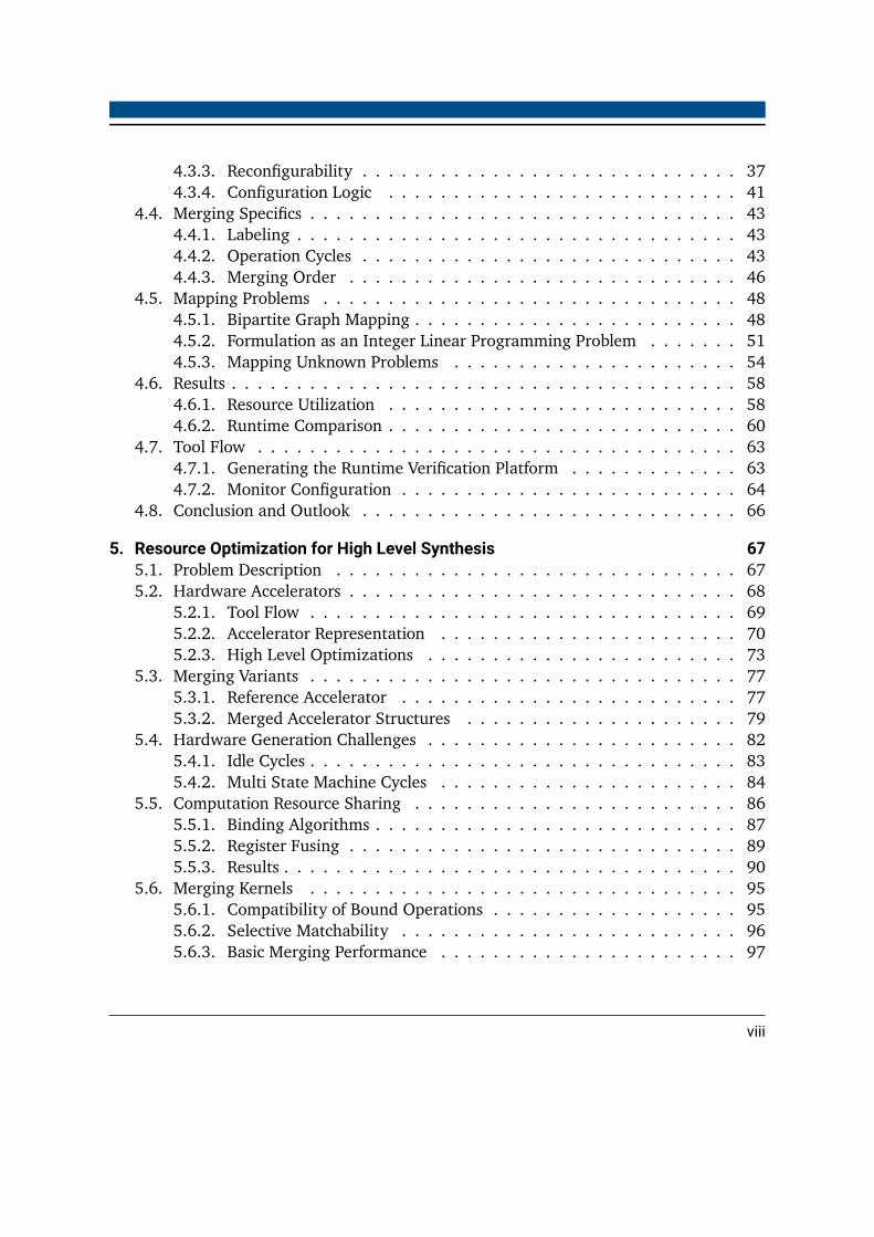
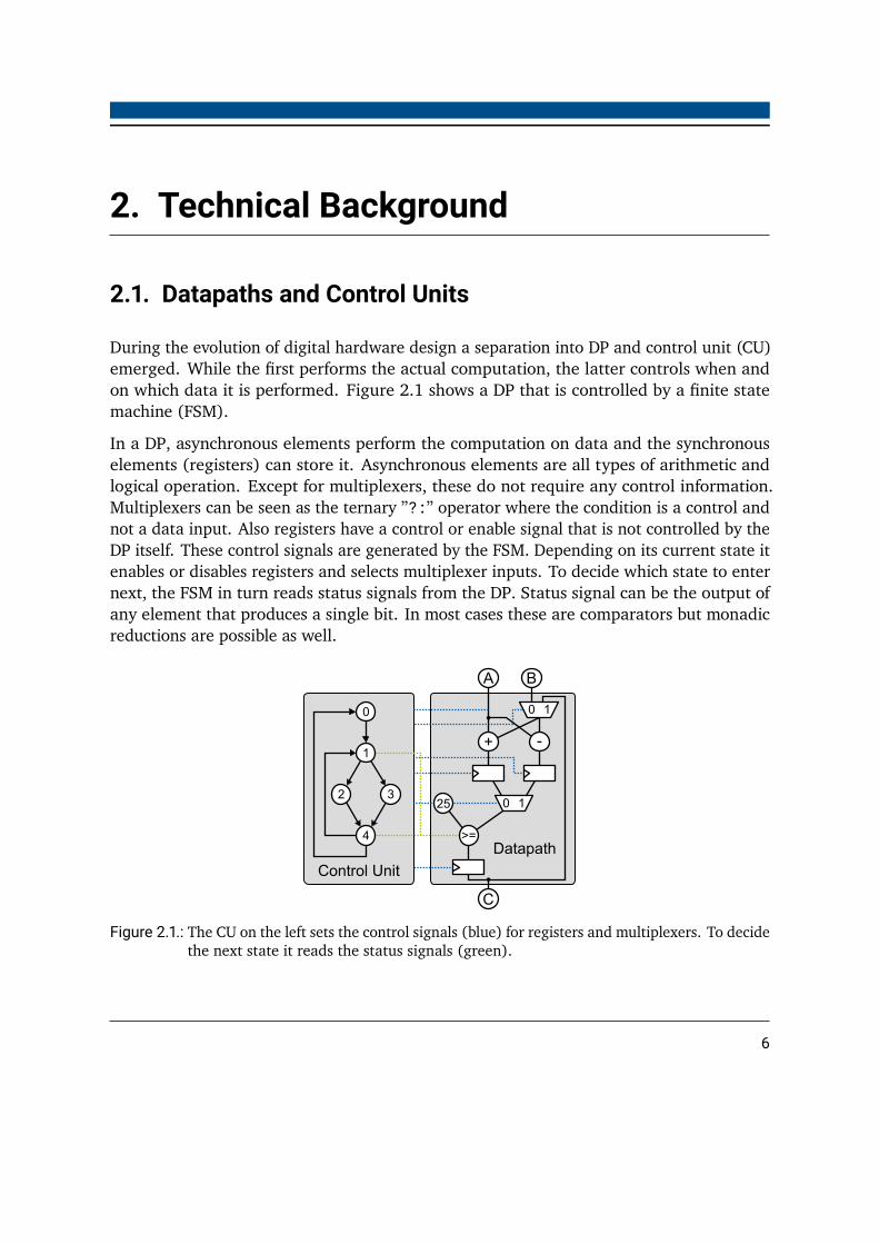
During the evolution of digital hardware design a separation into DP and control unit (CU)emerged. While the first performs the actual computation, the latter controls when andon which data it is performed. Figure 2.1 shows a DP that is controlled by a finite statemachine (FSM).
In a DP, asynchronous elements perform the computation on data and the synchronouselements (registers) can store it. Asynchronous elements are all types of arithmetic andlogical operation. Except for multiplexers, these do not require any control information.Multiplexers can be seen as the ternary ”?:” operator where the condition is a control andnot a data input. Also registers have a control or enable signal that is not controlled by theDP itself. These control signals are generated by the FSM. Depending on its current state itenables or disables registers and selects multiplexer inputs. To decide which state to enternext, the FSM in turn reads status signals from the DP. Status signal can be the output ofany element that produces a single bit. In most cases these are comparators but monadicreductions are possible as well.
>=
0 1
A
+ -
B
25
C
0
1
4
32
Control Unit
Datapath
0 1
Figure 2.1.: The CU on the left sets the control signals (blue) for registers and multiplexers. To decidethe next state it reads the status signals (green).
6
2.2. Graph Terminology
Throughout this thesis, lots of graphs with different characteristics will be shown. Todescribe these as accurately as possible, some mathematical terms must be introduced.Graphs generally consist of vertices (or nodes) and edges in-between them such that anedge has exactly one source and one destination node. In a graph Gx the node set is Nx
and the edge set is Ex.
Two major graph classes are directed and undirected graphs. They differ by the type ofedges, also directed or undirected, that are used to connect nodes. Only one type of edgesis allowed within a graph if it belongs to one class. If edges have a direction, it always pointsfrom the source towards the destination node. For undirected edges these roles can beswitched and are only used to distinguish the nodes from each other.
Two nodes in an undirected graph are called adjacent when they are connected by an edge.In case of a directed graph the source node of an edge is only adjacent to its target nodebut not vice versa - as long as no edge in the other direction exists.
A graph can be a simple graph when two nodes are never connected by more that oneedge. Edges that connect a node to itself, meaning that source and destination are equal,are called loops and are not allowed in simple graphs. Multigraphs allow multiple paralleledges in-between nodes and pseudographs additionally allow loops.
A subgraph Gsub is a graph that contains a subset of nodes and edges of the original graphGorig. When a subgraph is induced, it may not contain nodes or edges that are not inGorig. Furthermore, when an edge in Eorig has its source and destination in Nsub it must becontained in Esub.
The inverse or complement Ginv of a graph Gorig contains the same nodes (Ninv = Norig).Nodes that were adjacent in Gorig are not adjacent in Ginv and vice versa.
The degree of a node is the number of edges that touch the node. In directed graphs thiscan be subdivided into the in-degree, only counting edges pointing towards the node, andthe out-degree that only counts edges pointing away from the node.
An undirected graph in which all nodes are adjacent to each other is called complete. Ingraph theory an induced subgraph with this attribute is named clique.
Coloring a graph means that every node is assigned with a color in a way, that no twoadjacent nodes have the same color. The minimum number of colors for which a valid
7
AB
C D
E
FG
H
I
K M
N
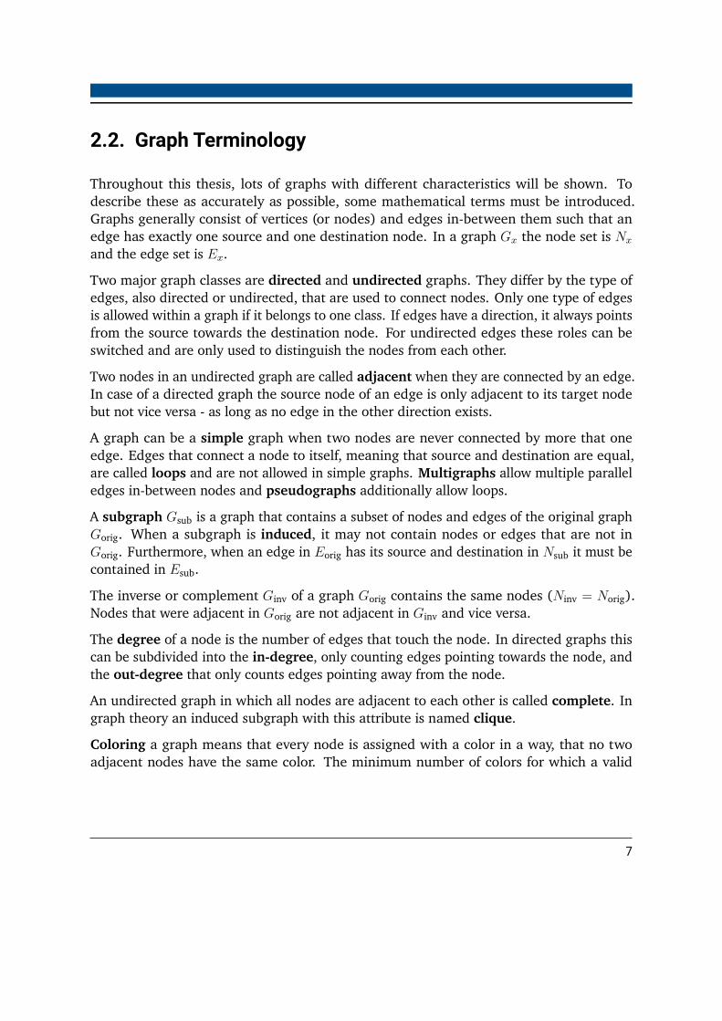
Figure 2.2.: A random graph. One maximal clique in blue is (F,K,M,N) and the maximum cliquein green is (B,C,E, F,G,H, I).
solution exists is called chromatic number. A clique of size S always requires exactly S
different colors to fulfill the previous statement.
Graphs are perfect when in every induced subgraph the chromatic number is equal to thesize of its largest clique. This requirement must also be fulfilled by the graph’s inverse.Problems that are NP complete for general graphs often have polynomial solutions whenthe graph is known to be perfect.
Bipartite graphs are a special class and consist of two node sets NA and NB. Edges onlyexist in-between the sets and never within a single one. Thus, an edge EA0EB5 can existbut EA0EA3 is not allowed.
Cliques As mentioned above, a clique is a set of nodes in which every node is adjacent toevery other node. Two special characteristics of cliques have to be mentioned. A clique iscalled maximal when no more nodes can be added. Thus, there exists no larger clique thatcontains all nodes of this clique. In Figure 2.2 one maximal clique of size four is formed by(F,K,M,N).
Usually, there is not only one but several maximal cliques inside one graph. The clique thatis constructed by the largest number of nodes is called the maximum clique. Although thenumber of maximum cliques is less than the number of maximal ones, there can be more thanone. The maximum clique in Figure 2.2 has size seven and is formed by (B,C,E, F,G,H, I).Since Groetschel et. al published [11] and [12] it is known that finding the maximum cliquein a general graph is an NP-complete problem.
8

A B
+
>=
C
25
01
10
0
(a) DFG with two inputs, a constant, two opera-tions, and one output. The numbers indicatethe destination nodes’ input port number.
A B
+
>=
C
25
01
10
0
-0
1
0
(b) A DPG similar to the DFG in (a). The outputsof both the addition and the subtraction pointtowards port 0 of the comparison.
Figure 2.3.: Comparison between a data flow graph and a data processing graph: The data processinggraph supports multiple edges pointing towards the same input of a node.
2.3. Datapath Abstraction
The DP+CU model is an accurate representation of the hardware implementation. Onecould directly write a Verilog module that implements the DP. However, this model containstoo much information when it comes to merging multiple DPs into a single (reconfigurable)DP. Thus, throughout literature ([3, 4, 5]) DFGs are used as an abstraction. These DFGsonly represent the asynchronous structure of a DP and omit all control and timing relatedinformation and the CU is not taken into account at all.
Data flow graphs are directed graphs of nodes and edges. Nodes are called activities,actors, or tasks. In our case they stand for operations to be performed on the incoming data.The edges represent the directed flow of data from one node to another. Operations aresolely controlled by the availability of data. [13, p. 54]1
Because the graphs shown in this work are not fully compatible to the DFG definition, theterm data processing graph (DPG) is used. Especially, the last characteristic of the DFGs isa difference to the DPGs. Although literature does not explicitly state so, nodes in a DFGusually only have one incoming edge per operand or port. The used graphs may have moreincoming edges on a single port.
1Translated.
9

The difference between a DFG and a DPG can be seen in Figure 2.3. In the latter one theinput at port 0 of the comparison can be the output of either the addition or the subtraction.If execution of operations only depended on the availability of input data, the addition andsubtraction of the DPG would always be executed simultaneously. Thus, the subsequentcomparison operation would somehow have to decide which data to process. Therefore,these edges must be resolved by inserting multiplexers when a DPG is to be turned into aDP. It can be seen that DFGs are a special form of DPGs and thus only the term DPG is usedfrom now on.The nodes of a DPG used in this thesis can be of the following types:
• Input Node:Data that is delivered from the outside into the DPG. It has no incoming edges.
• Output Node:Data that is delivered from the DPG to the outside. It has no outgoing edges.
• Constant Node:A constant value. It has no incoming edges.
• Operation Node:Performs an arithmetic or logic operation on the incoming data. It has at least oneincoming edge and one outgoing edge. The performed operation is given by the node’ssub-type.
10

3. Fundamentals of Datapath Merging
3.1. Compatibility Graphs
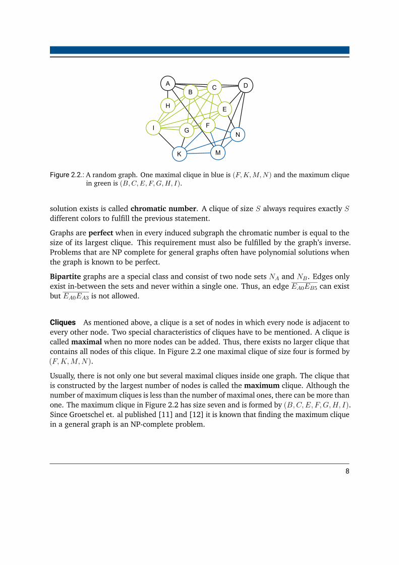
The first approach using CGs as an intermediate representation for merging DPs waspresented 2002 in [3]. Moreano et al. try to identify a set of nodes that can be sharedacross multiple DPGs because nodes in a DPG will later result in resources in the DP. Astheir concept is essential to this work some terms must be explained first. Throughout thisSection, DPGs are noted as DPGa and nodes of a graph as ai.
Matchability Two nodes are called matchable when they both implement the exact samefunction and thus can substitute each other. This is the case if the following criteria arefulfilled. First, their node types (see Section 2.3) must be the same. If the node is anoperation node, their operations must be the same as well. Hardware resources thatcombine different operations like (+/−) used in [4], are not considered. Second, the bitwidths of the operations have to be equal. Then, it depends on whether the later hardwareimplementation of the operation depends on the signedness. Additions or subtractions forexample are implemented in the same way irrespective of the signedness of their inputsand output. In case signedness matters, they must be equal as well.
When the nodes ai ∈ DPGa and bj ∈ DPGb fulfill all the above requirements, they forma matching noted as (ai|bj). Every matching can be seen as two operations that will laterin the DP be executed on the same resource. Testing all nodes of DPGa for matchabilitywith all nodes in DPGb will lead to a set S of matchings with |S| < N(DPGa) ∗N(DPGb)
where N(DPGx) is the number of nodes in DPGx.
Compatibility Not all matchings found in S can be applied concurrently. A node of DPGa
may only be matched to exactly one node DPGb and vice versa. Matchings that violate thisrule are said to be incompatible to each other. To represent these relationships betweenmatchings, CGs are used. Every matching in S is represented as a compatibility node (CN)in the CG. Therefore, the notation of CNs is the same as for matchings. Furthermore, a CN’stype is said to be the type of its nodes in the DPG.
11
O
a0 a1In In
# a2+ a3
+ a4
a5
(a) DPGa
^
O
b0 b1in in # b2
+ &b3 b4
b5
b6
(b) DPGb
a0|b0a1|b1
a0|b1a1|b0
a2|b2a5|b6 a4|b3a3|b3
(c) Basic compatibility graph ofDPGa andDPGb.A possible clique of size five is marked in yel-low.
a0/b1in
a1/b0in #
a2/b2
O a5/b6
+a3/-- & --/b4
a4/b3 + ^--/b5
(d) Resulting data processing graph after merging.
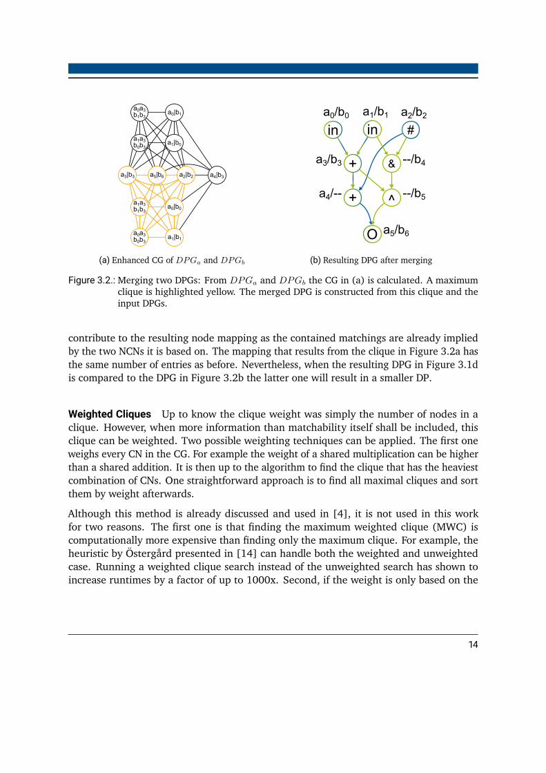
Figure 3.1.: Two data processing graphs (a) and (b) are merged into one. The compatibility graph isformed of matchable nodes of the DPGs and the resulting merged DPG.
Assume, the two DPGs in Figure 3.1a and 3.1b should be merged. All operator-, input-,and output bit widths are equal in this example and, due to carefully chosen operations,signedness is not of interest. The input nodes a0 and a1 are matchable with both b0 and b1and thus result in four CNs. The outputs a5 and b6 are matchable as well as the constantnodes a2 and b2. Both additions a3 and a4 can be matched with b4. Figure 3.1c shows theresulting CG containing the seven CNs.
Although the CG is relatively dense, some incompatibilities (or conflicts1) exist. For example,the matching (a4|b3) cannot be applied together with (a3|b3) and thus their CNs are notconnected in the CG.
After constructing the CG, a set of CNs has to be chosen to create a final mapping and thereby1It is also possible to formulate this problem as a conflict graph, which is the inverse of the compatibilitygraph.
12
select the shared operations. Within this set no incompatibilities are allowed. Reformulatedinto graph terminology, it means that the induced subgraph of the selected nodes must becomplete. From Section 2.2 this is known to be a clique.
Of course, one will always try to find the largest clique in the CG to get a high number ofshared operations. In Figure 3.1c one possible clique is highlighted. Using this clique, themapping ((a1|b0), (a0|b1), (a2|b2), (a5|b6), (a3|b4)) of size five is found.
From this mapping in conjuncton with the two input DPGs the merged DPG in Figure 3.1dcan be constructed. At first, all shared operations that are contained in the clique areinserted into a new graph. Afterwards, the remaining nodes of DPGa and DPGb are added.As a last step, the edges of the input DPGs are constructed. It must be considered, thatan edge may already exist between two nodes because its source and destination may beshared operations that are already connected.
3.1.1. Weighting Compatibility Graphs
Unfortunately, taking only nodes that are matchable into account can lead to sub-optimalresults. In Figure 3.1 it becomes obvious that selecting a3 to be matched with b3 should bepreferred over a4 as their predecessor nodes are shared as well. Two multiplexers will berequired in the DP to select the correct inputs for the addition (a4|b3). Both could be ommitedif the connections between the inputs and the addition are shared as well. Nevertheless,taking only the information given by the CG into account, the preferable solution is notsuperior to the found one. Choosing (a3|b3) over (a4|b3) also leads to a clique of size fivewhich is of equal value as the one previously found. Therefore, Moreano et. al proposedlater in [4] to enhance their first model by introducing edge matchability. The introducedCNs for matchable nodes are from now on called node compatibility nodes (NCNs).
Edge Matchability Two edges are matchable when their source nodes as well as theirdestination nodes are matchable. Furthermore, their destination ports have to be equal ifthe destination nodes’ operation is not commutative. When the edges ak → al and bm → bnare matchable the CN is called an edge compatibility node (ECN) and noted as (akal|bmbn).
An ECN is always compatible to the two source and destination NCNs. It is also compatibleto the intersection of the two sets of CNs adjacent to (ak|bm) and (al|bn). Hence, an ECNcan always be added to the clique if its constructing NCNs are selected. The ECN artificiallyincreases the size of the clique containing (a3|b3). Artificially, because an ECN itself does not
13
a4|b3a2|b2a5|b6
a0|b0
a1|b1a0a3b0b3
a1a3b1b3
a0|b1
a1|b0
a0a3b1b3
a1a3b0b3
a3|b3
(a) Enhanced CG of DPGa and DPGb
a0/b0in
a1/b1in #
a2/b2
O a5/b6
+a3/b3 & --/b4
a4/-- + ^--/b5
(b) Resulting DPG after merging
Figure 3.2.: Merging two DPGs: From DPGa and DPGb the CG in (a) is calculated. A maximumclique is highlighted yellow. The merged DPG is constructed from this clique and theinput DPGs.
contribute to the resulting node mapping as the contained matchings are already impliedby the two NCNs it is based on. The mapping that results from the clique in Figure 3.2a hasthe same number of entries as before. Nevertheless, when the resulting DPG in Figure 3.1dis compared to the DPG in Figure 3.2b the latter one will result in a smaller DP.
Weighted Cliques Up to know the clique weight was simply the number of nodes in aclique. However, when more information than matchability itself shall be included, thisclique can be weighted. Two possible weighting techniques can be applied. The first oneweighs every CN in the CG. For example the weight of a shared multiplication can be higherthan a shared addition. It is then up to the algorithm to find the clique that has the heaviestcombination of CNs. One straightforward approach is to find all maximal cliques and sortthem by weight afterwards.
Although this method is already discussed and used in [4], it is not used in this workfor two reasons. The first one is that finding the maximum weighted clique (MWC) iscomputationally more expensive than finding only the maximum clique. For example, theheuristic by Östergård presented in [14] can handle both the weighted and unweightedcase. Running a weighted clique search instead of the unweighted search has shown toincrease runtimes by a factor of up to 1000x. Second, if the weight is only based on the
14
operation type that is shared, the results are unlikely to change due to the CG’s structurewhich is explained in the following section.
The second approach is to weight the edges between CNs. This method would dispense theneed for inserting ECNs to the CG. A heavy weighted edge between two NCNs has the sameeffect as an additional ECN. Whenever both NCNs are selected, the weight of the cliqueis increased by more than the sum of their node weights. Although this might reduce theCG’s size, adding an ECN to the CG has two advantages. First, it can put additional weighton a combination of three or more nodes without adding weight to their individual pairs.Weighted edges can only make the combination of exactly two CNs heavier. Second, thenumber of edges in a CG is much larger than the number of nodes - N ∗ (N − 1)/2 in theworst case. This means that the input size for the maximum edge weighted clique (MEWC)problem is even bigger than for the MWC making it intractable for relevant problems.
15

a2|b2
a5|b6 a0|b0
a0|b1 a1|b1
a1|b0 a4|b3
a3|b3
(a) Conflict graph representation of Figure 3.1c.
a2|b2
a5|b6 a0|b0
a0|b1 a1|b1
a1|b0
a4|b3a3|b3
a0a3b0b3
a1a3b1b3
a0a3b1b3
a1a3b0b3
(b) Conflict graph representation of Figure 3.2aincluding matchable edges.
Figure 3.3.: The conflict graph shows clustering by node types which is harder to see in the CGrepresentation.
3.2. Structure of Compatibility Graphs
It can be said with certainty that CGs that are constructed from possible node matchingsfollow a structure. The first structural characteristic can be seen more easily when theconflict graph instead of the CG is considered. Figure 3.3 shows the conflict graph fromFigures 3.1c and 3.2a respectively. Especially, the first case demonstrates that conflicts onlyoccur between NCNs of the same type. If they are of a different type, the condition for aconflict can never be fulfilled. Only ECNs can lead to conflict ”bridges” between two clustersas they can conflict with the types of both their base NCNs.
This is the reason why weighting CNs only with respect to their operation types does notlead to improved results over an unweighted clique search. The weighting only has aneffect when there is the option to choose one heavier CN over two or more lighter CNs.For example one multiplication with a weight of 100 over two (compatible) additions witha weight of 25 each. However, this option does not exist in the constructed CGs becausethe clique searching algorithm ensures a maximal clique. The multiplication CN is alwayscompatible to both addition CNs which therefore will be selected as well.
This restricts the effect of node weighting to the conflict clusters. As these only containnodes of the same type, which also have the same weight, it makes the weighting ineffective.
16
A B
C
DE
F
(a) Chordal graph
A B
C
DE
F
(b) Weakly chordal graph
A B
C
DE
F
(c) Non chordal graph
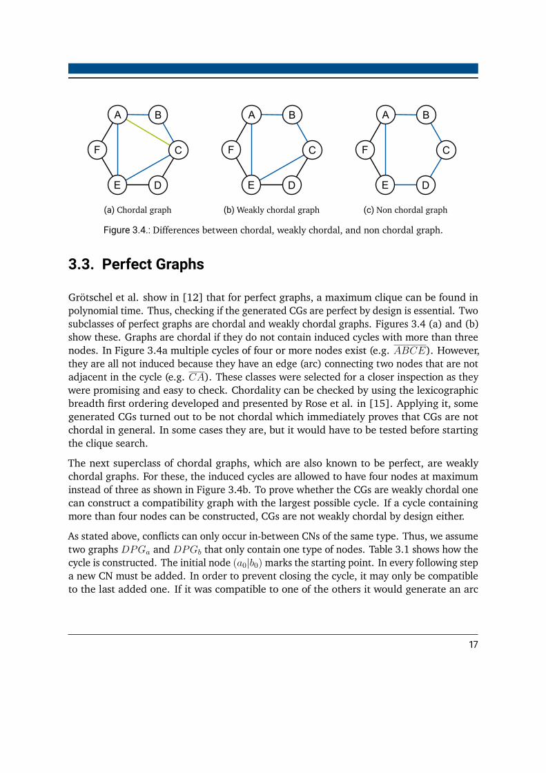
Figure 3.4.: Differences between chordal, weakly chordal, and non chordal graph.
3.3. Perfect Graphs
Grötschel et al. show in [12] that for perfect graphs, a maximum clique can be found inpolynomial time. Thus, checking if the generated CGs are perfect by design is essential. Twosubclasses of perfect graphs are chordal and weakly chordal graphs. Figures 3.4 (a) and (b)show these. Graphs are chordal if they do not contain induced cycles with more than threenodes. In Figure 3.4a multiple cycles of four or more nodes exist (e.g. ABCE). However,they are all not induced because they have an edge (arc) connecting two nodes that are notadjacent in the cycle (e.g. CA). These classes were selected for a closer inspection as theywere promising and easy to check. Chordality can be checked by using the lexicographicbreadth first ordering developed and presented by Rose et al. in [15]. Applying it, somegenerated CGs turned out to be not chordal which immediately proves that CGs are notchordal in general. In some cases they are, but it would have to be tested before startingthe clique search.
The next superclass of chordal graphs, which are also known to be perfect, are weaklychordal graphs. For these, the induced cycles are allowed to have four nodes at maximuminstead of three as shown in Figure 3.4b. To prove whether the CGs are weakly chordal onecan construct a compatibility graph with the largest possible cycle. If a cycle containingmore than four nodes can be constructed, CGs are not weakly chordal by design either.
As stated above, conflicts can only occur in-between CNs of the same type. Thus, we assumetwo graphs DPGa and DPGb that only contain one type of nodes. Table 3.1 shows how thecycle is constructed. The initial node (a0|b0)marks the starting point. In every following stepa new CN must be added. In order to prevent closing the cycle, it may only be compatibleto the last added one. If it was compatible to one of the others it would generate an arc
17
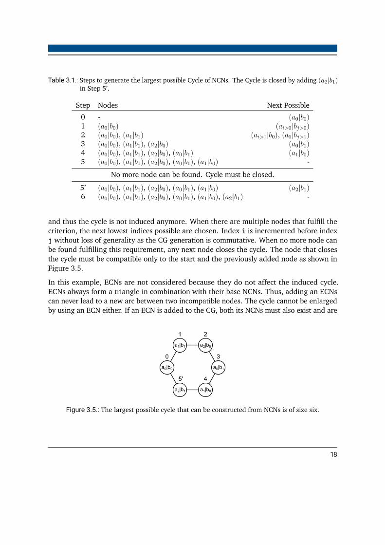
Table 3.1.: Steps to generate the largest possible Cycle of NCNs. The Cycle is closed by adding (a2|b1)in Step 5’.
Step Nodes Next Possible0 - (a0|b0)1 (a0|b0) (ai>0|bj>0)2 (a0|b0), (a1|b1) (ai>1|b0), (a0|bj>1)3 (a0|b0), (a1|b1), (a2|b0) (a0|b1)4 (a0|b0), (a1|b1), (a2|b0), (a0|b1) (a1|b0)5 (a0|b0), (a1|b1), (a2|b0), (a0|b1), (a1|b0) -
No more node can be found. Cycle must be closed.
5’ (a0|b0), (a1|b1), (a2|b0), (a0|b1), (a1|b0) (a2|b1)6 (a0|b0), (a1|b1), (a2|b0), (a0|b1), (a1|b0), (a2|b1) -
and thus the cycle is not induced anymore. When there are multiple nodes that fulfill thecriterion, the next lowest indices possible are chosen. Index i is incremented before indexj without loss of generality as the CG generation is commutative. When no more node canbe found fulfilling this requirement, any next node closes the cycle. The node that closesthe cycle must be compatible only to the start and the previously added node as shown inFigure 3.5.
In this example, ECNs are not considered because they do not affect the induced cycle.ECNs always form a triangle in combination with their base NCNs. Thus, adding an ECNscan never lead to a new arc between two incompatible nodes. The cycle cannot be enlargedby using an ECN either. If an ECN is added to the CG, both its NCNs must also exist and are
a0|b0
a1|b1 a2|b0
a0|b1
a1|b0a2|b1
0
1 2
3
45'
Figure 3.5.: The largest possible cycle that can be constructed from NCNs is of size six.
18

connected. This reduces the problem back to the original one without ECNs.
Up to now, no graph class with a maximum cycle size of six is mentioned in literature and itmust be assumed that they do not belong to the perfect graphs. To verify this assumption,an algorithm to check for general perfectness was implemented in [16]. The result was thesame as before - CGs are not generally perfect. Attempts to make CGs perfect by addingnodes or virtual edges did not succeed.
19

3.4. Clique Heuristic - QuickClique
Note: Parts of this chapter have already been published in [17]. To improve the reading flowself-citations are ommitted.
Although various clique heuristics already exist, it was decided in [16] to implement a newone. In the original publication it had no name but as the term heuristic occurs in morethan one context in this work it is from now on named QuickClique. The structure of theCGs and their high density allow numerous simplifications. Due to the clustering, it can beassumed that various maximum cliques of equal size exist. Furthermore, the heuristic’s goalis not to find the maximum clique at any cost. Of course, it is convenient to find a preferablylarge clique but it is not an absolute necessity for DP merging. A smaller clique will lead toless shared resources but the approach still works, even if no clique is found at all. Then,the resulting DP will contain two completely disjoint DPs without any shared resources -not practical but not wrong either.
The implemented heuristic is based on an upper and a lower bound for the clique size. Theupper bound has to be determined by an optimistic estimator while the lower bound is thelargest found clique yet. An accurate upper bound can be used as a figure of merit of thebest found solution. If a found clique has the size of the upper bound, the solution is knownto be a maximum clique. When the best found clique size is lower than the upper bound,there is either a larger clique in the graph, or the upper bound is higher than the maximumclique size. To obtain a close upper bound, the minimum of three following estimators isused.
1. Greedy Coloring:In literature that deals with clique finding algorithms often coloring is used for anupper bound. Using a greedy algorithm for coloring, the required number of colors isalways greater or equal to the maximum clique size.
2. “Square” calculation:Assume, the node with the highest degree in the graph has a degree of 25. Themaximum clique size could be 26 from that point of view. If there is no other nodewith such a high degree no clique with this size can be found. This can be continuedwith the node with the next lower degree until enough nodes with a sufficient degreeare found. Thereby, the maximum clique cannot be larger than the number of nodes|Nu| that have a degree of at least |Nu| − 1. A fast way to implement this estimator isto sort all nodes by their degree and afterwards iterate over this list. The first node
20
that has the same amount of predecessors in the list as its own degree marks the“square” point.
3. Gaussian Sum:In a fully connected graph, which is the same as a clique, the number of edges is calcu-lated by |E| = |N | ∗ (|N |−1)/2. In reverse, this means that solely the number of edgeslimits the number of possible fully connected nodes with |N | = ⌊
√︁2|E|+ 0.25 + 0.5⌋.
If a graph has in total 250 edges, the maximum clique size can never be greater than22, no matter how many nodes there are in the graph.
The clique search itself always tries to find a solution, that is better than the lower bound,namely the best yet found solution. It takes a node from the graph and tries to add nodesin descending degree order until no more node can be added. Afterwards, a clique mightbe improved by removing the node with the lowest degree and adding all other nodes thathave become compatible to the clique. If a better solution is found, it becomes the newlower bound.
The known lower bound allows to prune the graph, as no node that has a degree lower thanthe lower bound minus one will ever occur in a larger clique. Those nodes are removedfrom the graph to narrow down the search space. As all edges touching the pruned nodesare removed as well this procedure can reduce the upper bound. Adapting it during theclique search process can further increase the notion about the found solution’s quality. Thepruning also reduces the degree of other nodes leading to a new order for the node selection.It is most likely the reason why the implemented heuristic is much faster than comparableheuristics. One popular tool for example is cliquer. It uses the heuristic developed byÖstergård [14] which has polynomial complexity. Depending on the input graph, theruntimes of cliquer vary strongly and can reach more than 24 hours. On average, theruntime of the presented heuristic is about 40 times faster. Furthermore, it produces thesame or even a better result in 50% of the tested cases.
To get a notion about the result quality, QuickClique was evaluated against the exact solutionfor (random) graphs of 30 to 60 nodes with a normalized edge density of 0.9. In 91% ofthe cases the exact solution was found and in the other cases it was off by only one node.For the largest CG constructed of two DPGs, consisting of 2,092 nodes and 1,500,917 edges,the deviation was less than 7 nodes from the upper bound. Applied to the DIMACS2 [18]benchmark suite, the result quality of QuickClique varied between finding the best knownsolution and up to 25 nodes difference. The better result quality for the synthetic tests ismost likely caused by the higher edge density.
21
4. Runtime ReconfigurationNote: Parts of this chapter have already been published in [17, 19, 20]. To improve the readingflow self-citations are ommitted.
4.1. CONIRAS Project
This chapter is based on the work during the CONIRAS project which was funded by theGerman Federal Ministry for Education and Research with the funding ID 01IS13029D.CONIRAS stands for Continuous Non-Intrusive Runtime Analysis of SoCs. Its goal was tomake long-term observation and analysis of software in embedded systems possible by usingthe parallel processing capabilities of FPGAs.
4.1.1. Runtime Verification
Safety critical applications such as avionics and automotive put high requirements on therobustness and predictability in embedded software systems. Unit and integration testingstrongly reduce the number of software defects but their complete absence can only beshown by formal verification [21]. Because this is a time-consuming and expensive process,it is most exclusively used in military or space grade applications. Furthermore, until now noformal methods exist to verify multi core systems. Two applications running on a multi coresystem will influence each other because of deadlocks or race conditions. Timing behaviorcan also be affected due to parallel accesses on the memory, buses, or peripherals. Thus,the employment of multi core processors in embedded systems requires a lot more insightin order to find bugs than in single core setups. As there may be bugs that only occur undervery rare circumstances, the observation times must be much longer than for single coreapplications.
Instead of formal verification RV can be an appropriate tool to confirm or falsify a numberof assertions made by developers and testers. The SuT is observed for a preferably longtime period and checked for all made assumptions. If one of them does not hold, the causeof the deviating behavior can be inspected in detail.
22

Listing 4.1.: SALT [22] assertion to ensure doWork is only called while the program is executingExecute.
1 assert always (never call_doWork2 between inclusive optional return_Execute,3 exclusive optional call_Execute)
Some examples for possible assertions are given below:
1. When an interrupt request (IRQ) occurred, its corresponding interrupt service routine(ISR) must be entered after at most 10 µs.
2. A function may not be entered until the initialization is complete.
3. A thread must have at least 10% cpu time in a given time window.
4. Critical sections may not be entered by two threads concurrently.
5. A static variable may only be modified by a dedicated function.
6. …These assertions can be checked by so-called monitors that usually have a tri-state output.Either the assertion has been evaluated to be True, which can only happen if it has adedicated end point (e.g. assertion 2) or it can be Falsewhen the assertion has been violated.The third output is the Undefined output. Neither has the assertion been confirmed norfalsified up to that moment. One could say, that a monitor behaves like a labile system.In the beginning the state is Undefined and it can turn into either True or False. Whenone of the latter two is reached it stays there and cannot go back. In fact, in most casesthe outputs of the monitors will still have the Undefined output when the observation isfinished. These monitors indicate, that no violation has been seen and therefore, must beregarded as satisfied. Of course, this is only a valid assumption if the observation time ofthe SuT was long enough.
The basic monitor can be seen as an FSM with three different outputs. The inputs thattrigger the transitions are called propositions. In Listing 4.1 the propositions are thecall_<function> and return_<function> statements. The example uses SALT [22],which stands for Structured Assertion Language for Temporal Logic, to express monitors.The resulting FSM of the SALT compiler is given in Figure 4.1.
The question that arises is: Where does the information that leads to the propositions comefrom? One needs to know when a function was entered or left, when an interrupt occurred,
23

ST2
ST0
ST1
ST3
startc_do
c_ex
c_exr_ex
r_ex
c_do
c_ex
?
r_ex
Figure 4.1.: A monitor represented as an FSM. Yellow indicated states have the Undefined output,the red has the False output. The monitor can never evaluate to True as there is noaccording state. The propositions are abbreviated as follows: c_ex→call_execute,c_do→call_doWork, r_ex→return_execute.
which thread is currently running, and so forth. Code instrumentation can be used to obtainspecific information about the program flow for example. If the instrumentation is usedcarefully and only in locations of interest the amount of generated data can be kept low. Thedrawback using instrumentation is that it must not be removed after testing. This wouldhave again an effect on the timing behavior and therefore make the previous testing invalid.Thus, it introduces a runtime overhead during both testing and in-field use.
When lots of debug information has to be emitted the performance of the remaining programmay be decreased. For example, [23] showed that by generating a function call trace usingminimally invasive instrumentation (five assembly instructions) the runtime overhead wasalready 38%. At this level a faster and also more expensive processor becomes inevitable.For military or space grade applications this may be acceptable. In consumer applicationshowever, it is uneconomic to pay for more processing power that is only used for testingpurposes and thus neither required nor noticed by the end customer.
4.1.2. Project Setup
The hardware platform that is used in the CONIRAS project is shown in Figure 4.2 and canbe split into three major parts. An SuT containing a trace interface, the trace reconstruction,and the analysis. The latter can be either the RV or the worst case execution time (WCET)analysis. Depending on the used processor, the connection from the trace port to the FPGAcan vary from slower parallel interfaces to high speed serial connections. In this thesis the
24
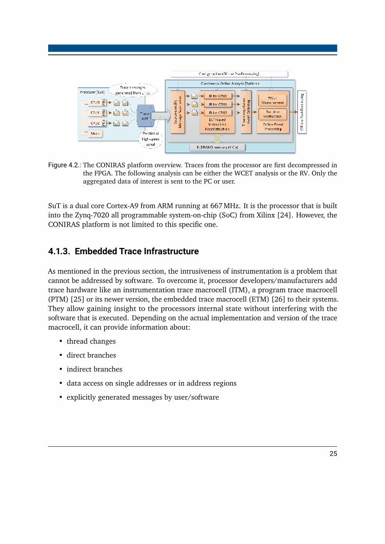
Figure 4.2.: The CONIRAS platform overview. Traces from the processor are first decompressed inthe FPGA. The following analysis can be either the WCET analysis or the RV. Only theaggregated data of interest is sent to the PC or user.
SuT is a dual core Cortex-A9 from ARM running at 667MHz. It is the processor that is builtinto the Zynq-7020 all programmable system-on-chip (SoC) from Xilinx [24]. However, theCONIRAS platform is not limited to this specific one.
4.1.3. Embedded Trace Infrastructure
As mentioned in the previous section, the intrusiveness of instrumentation is a problem thatcannot be addressed by software. To overcome it, processor developers/manufacturers addtrace hardware like an instrumentation trace macrocell (ITM), a program trace macrocell(PTM) [25] or its newer version, the embedded trace macrocell (ETM) [26] to their systems.They allow gaining insight to the processors internal state without interfering with thesoftware that is executed. Depending on the actual implementation and version of the tracemacrocell, it can provide information about:
• thread changes
• direct branches
• indirect branches
• data access on single addresses or in address regions
• explicitly generated messages by user/software
25
This trace information can, depending on the processor used, reach up to several Gbit/s. Forexample the macrocell implemented in the ARM processor has a 32 bit parallel output thatcan be clocked at up to 125MHz. It is directly connected to the FPGA fabric and accessibleas input/output (IO) pins. This allows easy access to the trace interface without any externalwiring, clock synchronization, or protocol. This rather small system can already lead todata rates of 4Gbit/s. Even though a regular desktop computer could possibly cope withthese data rates in terms of IO, online processing and analysis are impossible.
Therefore, currently available solutions from vendors like RAPITA are based on large storagearrays that have capacity to hold continuous traces for days [27]. Unfortunately, daysmay not be sufficient when testing a system in which errors may occur only under rarecircumstances. Its advantage over an online analysis is, that if an error occurs that was notcovered by any assertion, the stored information allows searching for its cause. A subsequentrefinement of assertions can be made to identify more possible situations in which this errormay appear. Nevertheless, analyzing this amount of data takes a long time. Depending onthe observation time and the frequency in which a bug occurs, most of the time is spentanalyzing information that is not of interest. Another major drawback of a storage systemsthat can hold more than a few seconds of trace data is its physical size. The amount ofraw trace data for a one day observation period (at 4Gb/s) is 43 TB, making hard disks orsolid state drives practically unavoidable. Such a system can most likely not be installed inplaces where embedded systems are used. Hence, in-field testing to have real IO conditionsbecomes nearly impossible.
The approach used in the CONIRAS project is to remedy both, the test system size andthe limited observation time problem. Continuously observing an SuT is made possible byutilizing the high processing capacity of FPGAs.
4.1.4. Trace Reconstruction
Unfortunately, although the trace interfaces have a high bandwidth, the data is still thor-oughly compressed. Particularly the information about the program flow is reduced toa minimum. Information is not sent for every executed instruction but only when a awaypoint (WP) is passed. WPs can be seen as the last instruction of a basic block (BB)and usually are conditional, direct, or indirect branches. Whenever a WP is passed, allpreceding instructions that belong to its BB are regarded as executed. In Listing 4.2 and itscorresponding simplified control flow graph (CFG) in Figure 4.3 multiple lines of the codeare mapped to a single WP event. Although this reduces the maximum time resolution, it isa safe upper bound until an instruction was executed.
26
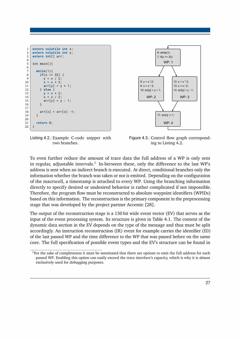
1 extern volatile int x;2 extern volatile int y;3 extern int[] arr;45 int main(){67 while(1){8 if(x >= 32) {9 y = x / 2;
10 x = x * 2;11 arr[y] = y + 1;12 } else {13 y = x * 2;14 x = x / 2;15 arr[y] = y - 1;16 }1718 arr[x] = arr[x] -1;19 }2021 return 0;22 }
Listing 4.2.: Example C-code snippet withtwo branches.
8: y = x / 2;
9: x = x * 2;
10: arr[y] = y + 1;
WP: 2
12: y = x * 2;
13: x = x / 2;
14: arr[y] = y - 1;
WP: 3
6: while(1)
7: if(x >= 32)
WP: 1
17: arr[x] -= 1;
WP: 4
Figure 4.3.: Control flow graph correspond-ing to Listing 4.2.
To even further reduce the amount of trace data the full address of a WP is only sentin regular, adjustable intervals.1 In-between these, only the difference to the last WP’saddress is sent when an indirect branch is executed. At direct, conditional branches only theinformation whether the branch was taken or not is emitted. Depending on the configurationof the macrocell, a timestamp is attached to every WP. Using the branching informationdirectly to specify desired or undesired behavior is rather complicated if not impossible.Therefore, the program flow must be reconstructed to absolute waypoint identifiers (WPIDs)based on this information. The reconstruction is the primary component in the preprocessingstage that was developed by the project partner Accemic [28].
The output of the reconstruction stage is a 130 bit wide event vector (EV) that serves as theinput of the event processing system. Its structure is given in Table 4.1. The content of thedynamic data section in the EV depends on the type of the message and thus must be splitaccordingly. An instruction reconstruction (IR) event for example carries the identifier (ID)of the last passed WP and the time difference to the WP that was passed before on the samecore. The full specification of possible event types and the EV’s structure can be found in
1For the sake of completeness it must be mentioned that there are options to emit the full address for eachpassed WP. Enabling this option can easily exceed the trace interface’s capacity, which is why it is almostexclusively used for debugging purposes.
27

Table 4.1.: Structure of the event vector input.
Field Bits Descriptionvalid 1 indicates if the current data is valid (1) or not (0)type 8 type of the event (thread change, program flow, …, see Table A.1)source 4 source of the event can be CPU0 to CPU7 or different ITMsdata 68 dynamic data depending on the typets_valid 1 valid bit for the timestamptimestamp 48 time at which the event occurred
Table A.1.
4.1.5. Runtime Verification Platform
As stated in Section 4.1.3, neither the compressed trace nor the decompressed eventscan be analyzed online by regular desktop computers. When the trace analysis is insteadperformed on the FPGA, numerous monitors implemented in hardware can analyze the traceinformation simultaneously. The major drawbacks in FPGA development are stated in manypapers dealing with it. First, it requires dedicated FPGA developers to implement the desiredfunctionality on the device. Although embedded software developers may already have abeneficial skill- and mindset, it will require more acquisition of knowledge to be able toimplement and optimize their designs. Thus, the more serious cause is that the turnaroundtimes are by orders of magnitude higher than in software development. When debuggingdesktop or embedded software it is simple to set break or watch points, inspect the callstack, and more. Setting a conditional break point is usually done in seconds for example.In FPGA development the time to synthesize designs can take up to several hours dependingon the size of the design and the targeted platform. Under certain conditions a design maynot reach the targeted clock frequency requiring another synthesis run. Considering thatRV is an interactive and iterative process, re-synthesizing the whole design every time anassertion is formulated or changed is not a feasible option.
The first problem is usually addressed by using either HLS compilers or a DSL. The HLSvariant, for which commercial tools already exist, is very generic and allows users to writea wide range of applications. A DSL however, can be more target-oriented and relieve aprogrammer from a lot of overhead. The DSL approach can also be more efficient in twoways. As it is tailored to specific requirements, it makes it easier for the user to formulate
28

SpartanMCCore
Eve
nt V
ecto
r
ConfigurationInterface
Monitor 0
Monitor 1
Monitor 2
Virtex 7 FPGA
FT2232H
Configuration
Analysis
Figure 4.4.: The RV platform.
his assertions correctly. Furthermore, the hardware that is generated by the compiler maybe more area efficient and can have a higher performance in terms of throughput.
The second problem cannot be solved by either of the two methods alone. Both rely on thesame synthesis process after the HLS/DSL code is transformed into hardware descriptionlanguage (HDL). In order to overcome high turnaround times, an¸ overlay architecturewas designed. Although the user does not explicitly implement any configuration featuresinto his monitors, the resulting hardware is runtime reconfigurable.2 The monitors are notdirectly translated into HDL but merged into one beforehand. The underlying principle isthat the merging process ensures that all given problems can be executed on it. Most likely,other similarly structured problems can also be mapped subsequently.
Figure 4.4 shows how the RV platform is structured. A SpartanMC soft core [29] basicallyacts like a router for information between the monitors and the host system. It has a customperipheral that controls an FTDI USB 2.0 chip [30]. When the host sends configurationdata a second peripheral is used to set the target monitor into configuration mode. Afterthe configuration is completed, the monitor is active and can emit events. These events arecollected by a funnel and sent back to the SpartanMC and again to the host PC.
2In [17] the overlay was called meta reconfigurable to respect the fact that the design has already beenimplemented on a reconfigurable device.
29
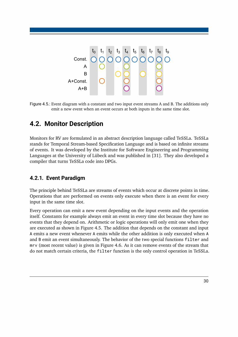
Const.
A
t0 t1 t2 t3 t4 t5 t6 t7 t8 t9
A+Const.
B
A+B
Figure 4.5.: Event diagram with a constant and two input event streams A and B. The additions onlyemit a new event when an event occurs at both inputs in the same time slot.
4.2. Monitor Description
Monitors for RV are formulated in an abstract description language called TeSSLa. TeSSLastands for Temporal Stream-based Specification Language and is based on infinite streamsof events. It was developed by the Institute for Software Engineering and ProgrammingLanguages at the University of Lübeck and was published in [31]. They also developed acompiler that turns TeSSLa code into DPGs.
4.2.1. Event Paradigm
The principle behind TeSSLa are streams of events which occur at discrete points in time.Operations that are performed on events only execute when there is an event for everyinput in the same time slot.
Every operation can emit a new event depending on the input events and the operationitself. Constants for example always emit an event in every time slot because they have noevents that they depend on. Arithmetic or logic operations will only emit one when theyare executed as shown in Figure 4.5. The addition that depends on the constant and inputA emits a new event whenever A emits while the other addition is only executed when Aand B emit an event simultaneously. The behavior of the two special functions filter andmrv (most recent value) is given in Figure 4.6. As it can remove events of the stream thatdo not match certain criteria, the filter function is the only control operation in TeSSLa.
30

Const.
t0 t1 t2 t3 t4 t5 t6 t7 t8 t9
X = A==Const.
6 6 6 6 6 6 6 6 6 6
A 6 3 6 5
B K L M N
T F T F
MRV(Filter) K K K K M M M
Filter(X, B) K M
Figure 4.6.: Event diagram showing the control functionality of a filter element and the storagecapability of the mrv element.
The mrv however is used to access data from past events. It constantly emits the value of thelast valid event. For example, if a time difference between two events shall be determined,the start time must be saved until the end time is known.
4.2.2. Application Scenario
A possible scenario that performs checks on the runtime of a function is given in Listing 4.3.The monitor serves two different purposes. It calculates the amount of time the programwas in a specific function and checks whether the function was executed within 10 µs. Theinputs given in lines 1 and 2 are strongly simplified. This information must be extractedfrom the event vector’s fields. A WPID for example is only contained in branching eventsand must be filtered first. Furthermore, this formulation assumes, that the trace is observedfrom the start. Starting the analysis while the trace is already running would have to take afunction exit without an entering into account. Additionally, when the function is entered itis always exited later and it is a non-recursive function.
Lines 6 and 7 define the entry and exit of the function and line 8 sets the upper limit forits execution time. The WPIDs for the comparison are are calculated from the waypointstatement. In order to avoid modifying the source code, it resolves the line in a file withthe corresponding WPID. The time function is necessary as the constants are unitless andneed to be converted to the time base of the SuT. The formula N = T ∗ fclk and the clockfrequency of 667Mhz turns the 10µs into 6670 cycles. The maximum time resolution isgiven with 1
fclk≈ 1.5ns.
31

Listing 4.3.: A simplified TeSSLa example to check the overall runtime of a function in a programand test for timing violations.
1 input wp_id;2 input timestamp;3 output execution_sum;4 output limit_exceeded;56 enter_function_id := waypoint(main.c:235);7 exit_function_id := waypoint(main.c:317);8 time_limit := time(10); //unit is us9
10 entry := equals(wp_id, enter_function_id);11 exit := equals(wp_id, exit_function_id);1213 entry_timestamp := delay( filter(entry, timestamp) );14 delta_time := sub(timestamp, entry_timestamp);15 function_execution_time := filter( exit, delta_time);1617 execution_sum := sum(function_execution_time);18 limit_exceeded := greater(function_execution_time, time_limit);
For a better understanding Figure 4.7 shows how a series of events are processed. In t0 thefunction is entered (WPID 1) and in t3 it is exited (WPID 2). It is entered again in t6. The twoevents in-between have different WPIDs and are not of interest for the function’s executiontime. The entry and exit point comparisons (equals) emit an event whenever there is anew WP event. Their output event contains the information about whether the accordingWP was passed. Based on that information the first filter discards all timestamps that arenot caused by the entry WP. The mrv stalls the event for one time slot and stores the valueto be accessible by later occurring events. In time slot t0 the sub does not execute becauseit depends on both, the timestamp and the delayed timestamp. Only after the mrv startsemitting events, the subtraction calculates the difference between the current timestampand the stored one.
The second filter then discards all the events from the subtraction unless the second WPis passed in t3. This results in the function’s execution time which is then compared againstthe limit. In this example, the filter could also be used before the sub and achieve thesame functionality. The comparison only emits an event in t3 when the function executiontime is calculated. The aggregation continuously outputs its current value as an eventbecause it has a defined output right from the beginning of the stream. After the programterminates the function’s portion of the total runtime can be calculated.
There are more functions like the sum function that are basically a macro for an operationand a mrv with a feedback. During the project time, cycles inside the monitor description
32

Entry
Exit
MRV
Sub
Greater
Sum
Timestamp
Waypoint
Filter13
Filter15
Y
2
TF F F
FF T FF
T
X
1
t0 t1 t2 t3 t4 t5 t6 t7
Y-X
0 0 0
Z
1
X Z
Y-X t-X
XXX X ZXX
t-? t-X Z-X
Figure 4.7.: The event diagram that can be constructed from the monitor description in Listing 4.3.The first event occurs at t0 and the last one at t7. Constants are omitted to improvereadability.
were not supported by TeSSLa. Therefore, it had to be implemented as an intrinsic function.
In this example it can be seen, that no explicit control flow exists. The execution of anoperation solely depends on the availability of events at its inputs. The control informationis veiled inside the operations themselves. For example, the filter discards events andthereby also disables subsequent operations. Because the control flow is implicitly involvedin the data flow, the graphs that represent the monitors are called control and data processinggraphs (CDPGs).
33

4.3. Event Processors
As stated in Section 4.1.5, it is not practicable to design only a single monitor, synthesizeit, and run the analysis. However, for the sake of understandability the following sectionsdescribe the process of turning a CDPG into a hardware monitor using a single CDPG.The result is called an event processor (EP) and implements the CDPG’s functionality inhardware.
4.3.1. Single Cycle Operation
To get a notion about how fast the trace events need to be processed by the monitors onecan look at the program flow trace. During the project it was expected, that the averageratio of WPs to all instructions in the code is between 1/4 and 1/5. This means that everyfourth or fifth instruction will result in a WP event. As a consequence, the event rate isdominated by the program flow trace events. Thread changes, interrupts, or user generatedmessages occur much less frequently and only play a secondary role. With the SuT runningat 667MHz the assumption gives an event rate between ≈130 and ≈170MEv/s for eachcore. This number is not entirely correct as the processor will sometimes, especially formemory accesses, need more than a single cycle to execute an instruction. Nevertheless, it isa good upper estimate of what the monitor system needs to be capable of. Later evaluationsin [32] revealed that a WP event is generated on average every 16 clock cycles. This mustbe seen as a lower estimate of what can be obtained because both the processor’s L2 cacheand the branch predictor were disabled. Therefore, throughout this chapter all generatedhardware is targeted to run with a 200MHz clock and must be able to handle a new eventin every cycle.
The single cycle requirement originates from the fact, that the EV has no back channel toindicate whether an event was accepted or not. A hypothetic ready signal would be the andcombination of all the EP’s local ready signals. Thus, a monitor requiring multiple cycleswould stall all other EPs and strongly reduce the achievable event processing rate. Adding afirst in first out (FIFO) buffer, which stores incoming events until they are processed, at theinput of such an EP does not improve this either. The problem is that the monitors cannotdecide in an early state which events are relevant or not. Therefore, processing an eventalways takes the same amount of time and the buffer will most probably overflow after ashort time.
34

Tim
esta
mp
==
==
>=
F
T-1
-
#
#
F
#
Sum
Exc
eed
WP
ID
Σ
Figure 4.8.: The strictly pipelined structure of the monitors allow events to be processed in everyclock cycle at more than 200MHz. Registers to keep the critical path preferably shortare marked in blue and pipeline synchronization registers in green.
Figure 4.8 shows the EP’s DP that implements the example given in Listing 4.3. Operationsthat modify the input data like the comparators or the subtraction have an output registerto keep the critical path as short as possible. For others, like the filters or delays this is notneeded as the only add or remove events.
There are also registers that are not required to achieve a high clock frequency. The secondregister that stores the current timestamp is not necessary to reduce the critical path length.Because data cannot be stored in a register for more than one clock cycle, it is required forsynchronization. The comparators that check if one of the two WPs has been passed have anoutput register. Thus, they delay the data by one clock cycle. In the path of the timestampno operation is performed until the T-1 block that represents the mrv function. Withoutthe additional register, the timestamp information would always be one clock cycle aheadof the WP information. A CU is not required for this DP to work as registers do not need(or are not allowed) to store information for more than one cycle. Multi cycle operationslike wide multiplications or a division are possible but they must have the same pipeliningcapabilities as the DP, namely, accepting new input data in every clock cycle.
4.3.2. Control/Valid Structure
The previous section showed how the data is processed by a static pipeline without a CU.However, it cannot work completely without a control structure. The event paradigm
35

OP &
D0 D1 V0 V1
VoutDout(a) Arithmetic or logic Op-
eration.
&
D1 D0 V0 V1
VoutDout(b) filter Function
D0 V0
VoutDout
en en
(c) mrv Function
VoutDout
D0 V0
+
1en
(d) sum Function
Figure 4.9.: Data and control structure of different operations and functions. Data flow is marked inblue and control flow in green.
explained in Section 4.2.1 requires an operation to know if an event occured and if it issupposed to operate. For this purpose every operation has a valid output signal that is setto 1 to indicate that it emitted an event. This signal must be passed through the pipelinesynchronously with its data. The logic that generates the valid signals for all operationsis called the valid tree. For stateful operations it is necessary to enable the data outputregister only when new events arrive, for others it is sufficient to only pass the valid signal.Stateful operations are the ones that store a value like the mrv or the min/max function.
Figure 4.9 depicts the four different possibilities for the valid structure of an operation.
(a) Data and valid signals are completely disjoint. The data output may have invalid datain-between events but will not be read.
(b) The valid signal also depends on the data output of the predecessor operation. Onlyapplies to filters.
(c) The output is constantly valid after the first valid input event.
(d) The operations output must constantly contain valid data and thus may only bechanged on an incoming event.
The valid tree is generated automatically from the input CDPG. In the beginning everyoperation has its complete valid logic without regarding its inputs. The resulting logic isvery naive and does not take into account that all valid signals in the end depend on theEV’s valid output. Therefore, all identities and equivalent registers are removed. In most
36
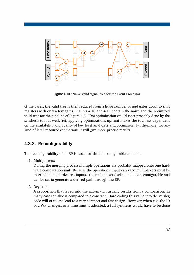
==
==
>=
F
T-1
-
#
#
F
#
Σ
Tim
esta
mp
Sum
&&
T-1&
Exc
eed
11
1
&
&&
1
WP
ID
Figure 4.10.: Naive valid signal tree for the event Processor.
of the cases, the valid tree is then reduced from a huge number of and gates down to shiftregisters with only a few gates. Figures 4.10 and 4.11 contain the naive and the optimizedvalid tree for the pipeline of Figure 4.8. This optimization would most probably done by thesynthesis tool as well. Yet, applying optimizations upfront makes the tool less dependenton the availability and quality of low level analyzers and optimizers. Furthermore, for anykind of later resource estimations it will give more precise results.
4.3.3. Reconfigurability
The reconfigurability of an EP is based on three reconfigurable elements.
1. Multiplexers:During the merging process multiple operations are probably mapped onto one hard-ware computation unit. Because the operations’ input can vary, multiplexers must beinserted at the hardware’s inputs. The multiplexers’ select inputs are configurable andcan be set to generate a desired path through the DP.
2. Registers:A proposition that is fed into the automaton usually results from a comparison. Inmany cases a value is compared to a constant. Hard coding this value into the Verilogcode will of course lead to a very compact and fast design. However, when e.g. the IDof a WP changes, or a time limit is adjusted, a full synthesis would have to be done
37
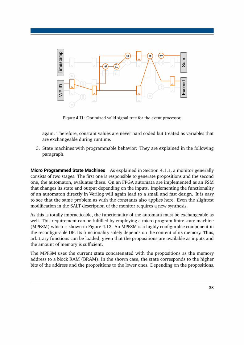
Tim
esta
mp
==
==
>=
F
T-1
-
#
#
F
#
Σ
Sum
&&
T-1&
Exc
eed
1
WP
ID
Figure 4.11.: Optimized valid signal tree for the event processor.
again. Therefore, constant values are never hard coded but treated as variables thatare exchangeable during runtime.
3. State machines with programmable behavior: They are explained in the followingparagraph.
Micro Programmed State Machines As explained in Section 4.1.1, a monitor generallyconsists of two stages. The first one is responsible to generate propositions and the secondone, the automaton, evaluates these. On an FPGA automata are implemented as an FSMthat changes its state and output depending on the inputs. Implementing the functionalityof an automaton directly in Verilog will again lead to a small and fast design. It is easyto see that the same problem as with the constants also applies here. Even the slightestmodification in the SALT description of the monitor requires a new synthesis.
As this is totally impracticable, the functionality of the automata must be exchangeable aswell. This requirement can be fulfilled by employing a micro program finite state machine(MPFSM) which is shown in Figure 4.12. An MPFSM is a highly configurable component inthe reconfigurable DP. Its functionality solely depends on the content of its memory. Thus,arbitrary functions can be loaded, given that the propositions are available as inputs andthe amount of memory is sufficient.
The MPFSM uses the current state concatenated with the propositions as the memoryaddress to a block RAM (BRAM). In the shown case, the state corresponds to the higherbits of the address and the propositions to the lower ones. Depending on the propositions,
38

Sta
te 0
Sta
te 1
Sta
te 2
000110110001101100011011
Block RAM
Add
ress
State Output
000000001000010
01001001010001010
010100011001100
1000100100010001100100011
PropositionsS P
Figure 4.12.: A micro program state machine consists of a BRAM and a feedback. Depending onthe content of the selected line and the propositions the new state and its output arechosen.
a line in the memory range that is addressed by the state is selected. It contains the nextstate and the output of the next state. Every time the input data is valid the current stateand the propositions are evaluated by enabling the address register.
Mainly three parameters have an influence on its characteristic.
• With an increased number of states (S) the address width and line size are bothincreased by ⌈log2(|S|)⌉.
• Every input proposition (P ) adds one more address line but has no influence on theline size.
• The number of different outputs (O) only increases the line size by ⌈log2(|O|)⌉.However, it was decided to use a one-hot encoding for the output as the number ofdifferent outputs is limited to three due to the SALT description.
39
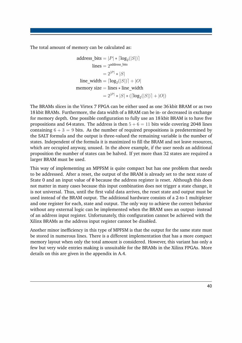
The total amount of memory can be calculated as:
address_bits = |P | ∗ ⌈log2(|S|)⌉lines = 2address_bits
= 2|P | ∗ |S|line_width = ⌈log2(|S|)⌉+ |O|
memory size = lines ∗ line_width= 2|P | ∗ |S| ∗ (⌈log2(|S|)⌉+ |O|)
The BRAMs slices in the Virtex 7 FPGA can be either used as one 36 kbit BRAM or as two18 kbit BRAMs. Furthermore, the data width of a BRAM can be in- or decreased in exchangefor memory depth. One possible configuration to fully use an 18 kbit BRAM is to have fivepropositions and 64 states. The address is then 5 + 6 = 11 bits wide covering 2048 linescontaining 6 + 3 = 9 bits. As the number of required propositions is predetermined bythe SALT formula and the output is three-valued the remaining variable is the number ofstates. Independent of the formula it is maximized to fill the BRAM and not leave resources,which are occupied anyway, unused. In the above example, if the user needs an additionalproposition the number of states can be halved. If yet more than 32 states are required alarger BRAM must be used.
This way of implementing an MPFSM is quite compact but has one problem that needsto be addressed. After a reset, the output of the BRAM is already set to the next state ofState 0 and an input value of 0 because the address register is reset. Although this doesnot matter in many cases because this input combination does not trigger a state change, itis not universal. Thus, until the first valid data arrives, the reset state and output must beused instead of the BRAM output. The additional hardware consists of a 2-to-1 multiplexerand one register for each, state and output. The only way to achieve the correct behaviorwithout any external logic can be implemented when the BRAM uses an output- insteadof an address input register. Unfortunately, this configuration cannot be achieved with theXilinx BRAMs as the address input register cannot be disabled.
Another minor inefficiency in this type of MPFSM is that the output for the same state mustbe stored in numerous lines. There is a different implementation that has a more compactmemory layout when only the total amount is considered. However, this variant has only afew but very wide entries making is unsuitable for the BRAMs in the Xilinx FPGAs. Moredetails on this are given in the appendix in A.4.
40
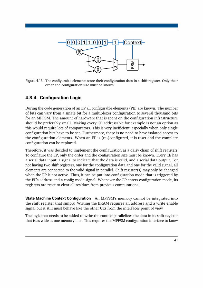
01
0 0 0 0 0 11 1 1
25
==
<=
Context
FSM
Figure 4.13.: The configurable elements store their configuration data in a shift register. Only theirorder and configuration size must be known.
4.3.4. Configuration Logic
During the code generation of an EP all configurable elements (PE) are known. The numberof bits can vary from a single bit for a multiplexer configuration to several thousand bitsfor an MPFSM. The amount of hardware that is spent on the configuration infrastructureshould be preferably small. Making every CE addressable for example is not an option asthis would require lots of comparators. This is very inefficient, especially when only singleconfiguration bits have to be set. Furthermore, there is no need to have isolated access tothe configuration elements. When an EP is (re-)configured, it is reset and the completeconfiguration can be replaced.
Therefore, it was decided to implement the configuration as a daisy chain of shift registers.To configure the EP, only the order and the configuration size must be known. Every CE hasa serial data input, a signal to indicate that the data is valid, and a serial data output. Fornot having two shift registers, one for the configuration data and one for the valid signal, allelements are connected to the valid signal in parallel. Shift register(s) may only be changedwhen the EP is not active. Thus, it can be put into configuration mode that is triggered bythe EP’s address and a config mode signal. Whenever the EP enters configuration mode, itsregisters are reset to clear all residues from previous computations.
State Machine Context Configuration An MPFSM’s memory cannot be integrated intothe shift register that simply. Writing the BRAM requires an address and a write enablesignal but it still must behave like the other CEs from the interfaces point of view.
The logic that needs to be added to write the context parallelizes the data in its shift registerthat is as wide as one memory line. This requires the MPFSM configuration interface to know
41

when the first line is complete. All succeeding lines are then aligned with the memory’s linewidth. To avoid counting the bits that must be sent until the first line arrives, a start bit iscontained in the configuration sequence. When this is detected at the end of the MPFSM’sshift register, it triggers the first write access. It is then reinserted to the beginning of thelocal shift register which is apart from that cleared. The write address is incremented aftereach write access until the end of the memory is reached. Afterwards, the start bit is passedto the serial output in case there are multiple state machines contained in the EP.
42

4.4. Merging Specifics
Themerging technique presented in Chapter 3 seems to be agnostic of implementation detailsat first. Nevertheless, this approach is very general and does consider all circumstances.This section therefore takes a look at some special characteristics of monitor merging.
4.4.1. Labeling
When a CDPG is read from the file the first step is to label every node N with its height H(N)
in the graph. Labeling starts at the output nodes which have a height of zero. From there allpredecessor nodes, of which all successors are already labeled, get the maximum height oftheir successors plus one. Thus, every node gets assigned its minimum height in the CDPG.This labeling can be seen as an as late as possible (ALAP) schedule. Any further scheduling isnot required as only the order in which the operations are performed is relevant. Therefore,the execution time (or delay) of an operation D(N) is also not considered. Otherwise,an operation that is purely combinatorial, like a filter, could have the same height as itssuccessor operation and their execution order could not be determined correctly.
The labeling is also applied on merged graphs before they are transformed into a Verilogmodule. Here, the execution time information is taken into account to calculate the numberof pipeline registers that need to be inserted between two operations. The height of a nodeis now the maximum height of all its successors plus its own delay D(N).
For every two adjacent nodes, the number of pipeline registers on their path can be calculatedas N = (H(Na) − H(Nb)) − D(Na). Apparently, this formula only makes sense whenH(Na) > H(Nb) meaning that Na is executed before Nb.
4.4.2. Operation Cycles
Using the compatibility rules from Section 3.1 cycles can occur in a merged CDPG due tothe operation ordering. Figure 4.14 shows how a cycle can be formed by two CDPGs thatcontain the same operations but in reverse order. This problem does not only arise whenoperations are directly subsequent but also if there are other operations in-between. Then,the cycle becomes larger. In most of the cases, this would not be a problem for synthesisbecause they are usually not purely combinatorial as most operations have an output register.The problem arises when the merged CDPG shall be labeled before the pipeline registers are
43
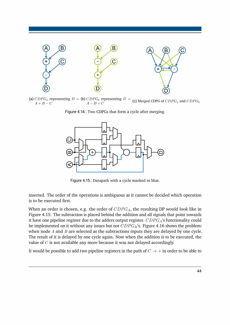
A B
+
-
D
C
(a) CDPGa representing D =A+B − C
A B
-
+
D
C
(b) CDPGb representing D =A−B + C
+ -
D
A B C
(c) Merged CDPG of CDPGa and CDPGb
Figure 4.14.: Two CDPGs that form a cycle after merging.
D+ -
AB
C
Figure 4.15.: Datapath with a cycle marked in blue.
inserted. The order of the operations is ambiguous as it cannot be decided which operationis to be executed first.
When an order is chosen, e.g. the order of CDPGA, the resulting DP would look like inFigure 4.15. The subtraction is placed behind the addition and all signals that point towardsit have one pipeline register due to the adders output register. CDPGA’s functionality couldbe implemented on it without any issues but not CDPGB ’s. Figure 4.16 shows the problem:when node A and B are selected as the subtractions inputs they are delayed by one cycle.The result of it is delayed by one cycle again. Now when the addition is to be executed, thevalue of C is not available any more because it was not delayed accordingly.
It would be possible to add two pipeline registers in the path of C → + in order to be able to
44
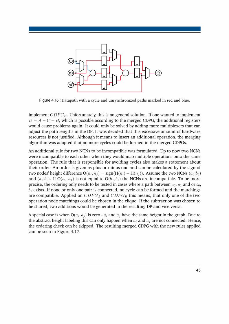
D+ -A
BC
Figure 4.16.: Datapath with a cycle and unsynchronized paths marked in red and blue.
implement CDPGB. Unfortunately, this is no general solution. If one wanted to implementD = A− C +B, which is possible according to the merged CDPG, the additional registerswould cause problems again. It could only be solved by adding more multiplexers that canadjust the path lengths in the DP. It was decided that this excessive amount of hardwareresources is not justified. Although it means to insert an additional operation, the mergingalgorithm was adapted that no more cycles could be formed in the merged CDPGs.
An additional rule for two NCNs to be incompatible was formulated. Up to now two NCNswere incompatible to each other when they would map multiple operations onto the sameoperation. The rule that is responsible for avoiding cycles also makes a statement abouttheir order. An order is given as plus or minus one and can be calculated by the sign oftwo nodes’ height difference O(ni, nj) = sign(H(ni)−H(nj)). Assume the two NCNs (a0|b0)and (a1|b1). If O(a0, a1) is not equal to O(b0, b1) the NCNs are incompatible. To be moreprecise, the ordering only needs to be tested in cases where a path between a0, a1 and or b0,b1 exists. If none or only one pair is connected, no cycle can be formed and the matchingsare compatible. Applied on CDPGA and CDPGB this means, that only one of the twooperation node matchings could be chosen in the clique. If the subtraction was chosen tobe shared, two additions would be generated in the resulting DP and vice versa.
A special case is when O(ai, aj) is zero - ai and aj have the same height in the graph. Due tothe abstract height labeling this can only happen when ai and aj are not connected. Hence,the ordering check can be skipped. The resulting merged CDPG with the new rules appliedcan be seen in Figure 4.17.
45
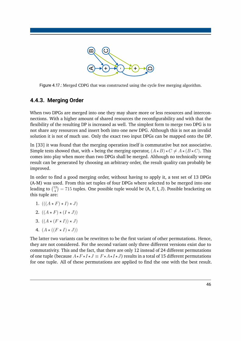
+ DAB C
+-
Figure 4.17.: Merged CDPG that was constructed using the cycle free merging algorithm.
4.4.3. Merging Order
When two DPGs are merged into one they may share more or less resources and intercon-nections. With a higher amount of shared resources the reconfigurability and with that theflexibility of the resulting DP is increased as well. The simplest form to merge two DPG is tonot share any resources and insert both into one new DPG. Although this is not an invalidsolution it is not of much use. Only the exact two input DPGs can be mapped onto the DP.
In [33] it was found that the merging operation itself is commutative but not associative.Simple tests showed that, with ⋆ being the merging operator, (A⋆B)⋆C ̸= A⋆ (B ⋆C). Thiscomes into play when more than two DPGs shall be merged. Although no technically wrongresult can be generated by choosing an arbitrary order, the result quality can probably beimproved.
In order to find a good merging order, without having to apply it, a test set of 13 DPGs(A-M) was used. From this set tuples of four DPGs where selected to be merged into oneleading to
(︁134
)︁= 715 tuples. One possible tuple would be (A, F, I, J). Possible bracketing on
this tuple are:
1. (((A ⋆ F ) ⋆ I) ⋆ J)
2. ((A ⋆ F ) ⋆ (I ⋆ J))
3. ((A ⋆ (F ⋆ I)) ⋆ J)
4. (A ⋆ ((F ⋆ I) ⋆ J))
The latter two variants can be rewritten to be the first variant of other permutations. Hence,they are not considered. For the second variant only three different versions exist due tocommutativity. This and the fact, that there are only 12 instead of 24 different permutationsof one tuple (becauseA⋆F ⋆I⋆J ≡ F ⋆A⋆I⋆J) results in a total of 15 different permutationsfor one tuple. All of these permutations are applied to find the one with the best result.
46

Afterwards, eight different heuristics were implemented to check whether the result qualitycan be estimated before the merging to avoid time-consuming maximum clique searches.A heuristic will estimate the quality of every pair of available CDPGs, including alreadymerged ones and choose the combination with the highest value for the next merging step.The heuristics can be summarized as following:
• Heuristic I: The size of the node set of the CG. A larger graph may indicate that theDPGs are very common.The clear drawback here is that larger input DPGs will be preferred over small DPGsas they will naturally have more operators and thus a higher chance for generatingCNs.
• Heuristic II: Normalize the number of CNs with the number of nodes of the DPGs totake different DPG size into account.
• Heuristic III: Divide the number of CNs by the number of edges in the CG. This edgedensity is an indicator of how many compatibilities exist for every CN.
• Heuristic IV: The same as Heuristic I but only considers NCNs.
• Heuristic V: The same as Heuristic II but only considers NCNs.
• Heuristic VI: In contrast to Heuristic IV it only counts ECNs.
• Heuristic VII: In contrast to Heuristic V it divides ECNs by the edges in the DPGs.
The tests revealed that the resulting merged DPGs do not differ in the number of sharedresources. This can be explained by the fact, that the maximum clique will always findthe maximum of shareable resources and the maximum operator in turn is associative.The results only differed by the number of multiplexers that have to be inserted in thereconfigurable DP. Overall the results did not deviate much from each other but Heuristic Vturned out to find the optimal merging order the most often. This is a bit counter-intuitivebecause Heuristic V does not take any matchable edges into account whereas in Section 3.1they are an essential component to obtain smaller resulting DPGs. However, they do notindicate a higher degree of similarity of two DPGs.
47
4.5. Mapping Problems
Note: The term matchability and compatiblity that were introduced in Section 3.1 are stillvalid.
Mapping a problem is the process that generates a configuration for an EP in order toexecute a given problem. It tries to map every node of the problem CDPG (CDPGp) onto aresource in the EP. Furthermore, it also maps all edges onto the physical interconnects. Theprerequisite for mapping a problem is the configuration information of a merged CDPG. Theinput problem can be either one of those that were used to generate the merged CDPG or adisjoint one. Given that all required resources and interconnects are available the problemcan be mapped. For problems that were used to create the EP, the required resources arealways available and accordingly, they are mappable.
As the EP is also represented by a CDPG (CDPGep) the mapping is similar to the mappingin the merging step. The major difference between the merging and the mapping is thecompleteness requirement. While merging two CDPGs, it is allowed that a node fromCDPGa has no matching node in CDPGb. The same applies for the edges. When mappinga new problem, this is not feasible. A matching node/edge must be found in CDPGep forevery node/edge in CDPGp - it must be complete from CDPGp’s point of view.
4.5.1. Bipartite Graph Mapping
To reduce the problem size, the node and edge mappability can be reduced to only thelatter one. As every node is the source or target node of at least one edge, the edgemappability includes the node mappability. To find a complete mapping, a bipartite graphas in Figure 4.18 is constructed. As explained in Section 2.2, a bipartite graph consists oftwo node sets Na and Nb and edges are only allowed in-between these. For the mapping,the sets are the input (problem) set Np and target set Nep. Every node in Np represents anedge in CDPGp. Analog to that, the same applies for Nep and CDPGep. Edges betweennodes in the bipartite graph represent matchability.
There are efficient algorithms to find a maximum matching in bipartite graphs. A maximummatching is the largest set of edges that do not connect one node in Na to more than onenode in Nb. For example Hopcroft and Karp present one with a polynomial runtime (|N | 52 )in [34]. When a complete matching (for CDPGp) exists this automatically is the maximummatching. This would make such an algorithm suitable in theory but nevertheless, it cannotbe applied.
48

ED E5
EAE2
E1
Np Nep
EC
E4
E3
EB
Figure 4.18.: Bipartite graph representing matchable edges for mapping problems. The grey markededge is an essential edge. A possible complete mapping is given by the highlightededges.
Although the constructed graph looks like a bipartite one, its edges contain more informationthan just matchability. Selecting an edge makes its touching nodes ”unusable” for furthermatchings and it may be removed. Furthermore, it also implies two node matchings thatmay be incompatible to the node matchings of other bipartite edges. All other edges thatobject a selected edge must be removed after each selection. No algorithm respecting theseincompatibilities is known to the author and no solution could be found modeling these in apurely bipartite manner. Therefore, it was decided to implement a backtracking algorithm.
The pseudo code for the implemented algorithm is shown in Algorithm 4.1. To improvethe runtime of the algorithm, an essential edge is selected if available. An essential edgeis an edge that belongs to a node in Np that has no other connections. In Figure 4.18 anessential edge is EDE5. As stated, for each node from Np a corresponding node in Nep mustexist. As a consequence, an essential edge always has to be chosen to obtain a completeresult. To ensure that the result is also valid, all edges that are incompatible with the currentchoice are removed. If no essential edges are available, one of the remaining edges has tobe selected. The selection is also not done randomly. Edges are sorted by a criterion so thathigher ranked edges are selected first. The overall performance of the mapping algorithmhas turned out best when the criterion is the incompatibility. This means that edges thatremove lots of incompatible edges from the bipartite graph have a high rank. It seems toresolve conflicts of highly demanded resources early and not push the decision down to theend of the computation. When no solution is found with this choice, it has to be rolled backand another edge is selected. If none of the possible edges has led to a solution, the inputCDFG is not mappable.
49
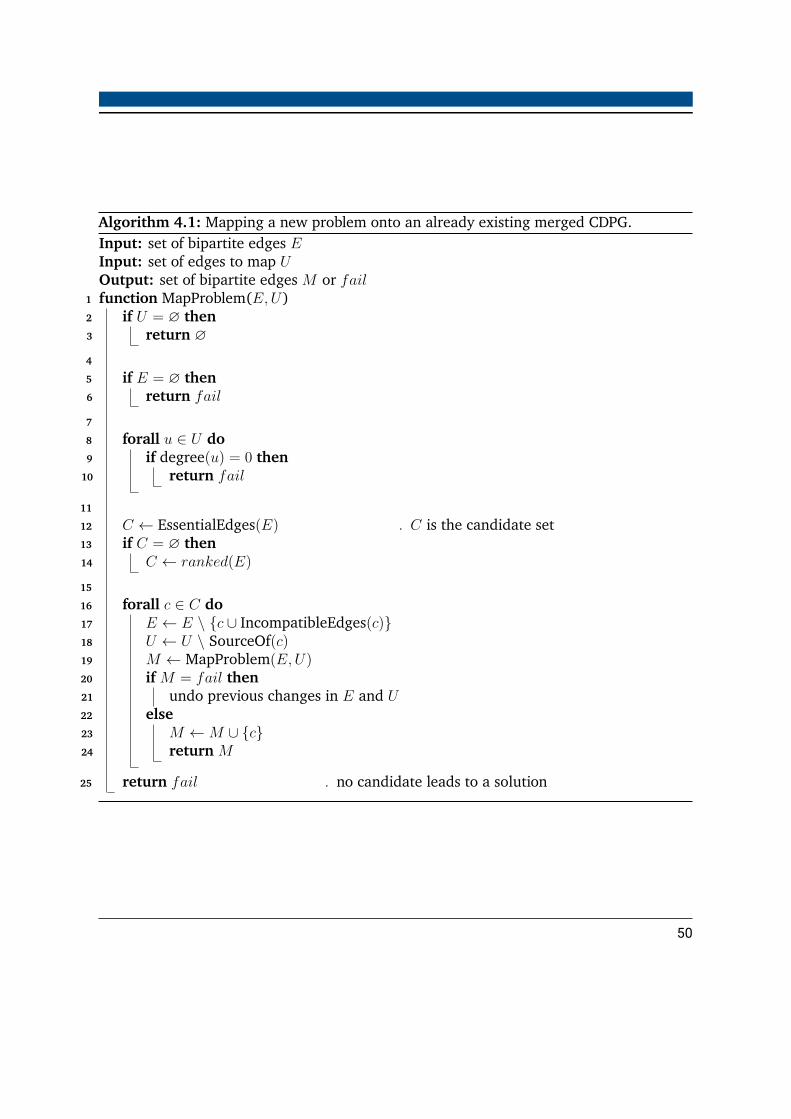
Algorithm 4.1: Mapping a new problem onto an already existing merged CDPG.Input: set of bipartite edges EInput: set of edges to map UOutput: set of bipartite edges M or fail
1 function MapProblem(E,U)2 if U = ∅ then3 return ∅4
5 if E = ∅ then6 return fail
7
8 forall u ∈ U do9 if degree(u) = 0 then
10 return fail
11
12 C ← EssentialEdges(E) ▷ C is the candidate set13 if C = ∅ then14 C ← ranked(E)
15
16 forall c ∈ C do17 E ← E \ {c ∪ IncompatibleEdges(c)}18 U ← U \ SourceOf(c)19 M ← MapProblem(E,U)20 if M = fail then21 undo previous changes in E and U22 else23 M ←M ∪ {c}24 return M
25 return fail ▷ no candidate leads to a solution
50
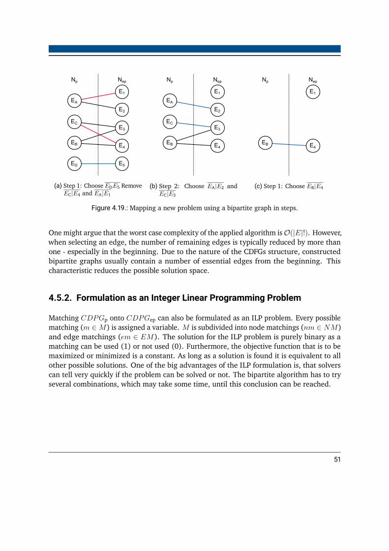
ED E5
EAE2
E1
Np Nep
EC
E4
E3
EB
(a) Step 1: ChooseEDE5 RemoveEC|E4 and EA|E1
EAE2
E1
Np Nep
EC
E4
E3
EB
(b) Step 2: Choose EA|E2 andEC|E3
E1
Np Nep
E4EB
(c) Step 1: Choose EB|E4
Figure 4.19.: Mapping a new problem using a bipartite graph in steps.
One might argue that the worst case complexity of the applied algorithm isO(|E|!). However,when selecting an edge, the number of remaining edges is typically reduced by more thanone - especially in the beginning. Due to the nature of the CDFGs structure, constructedbipartite graphs usually contain a number of essential edges from the beginning. Thischaracteristic reduces the possible solution space.
4.5.2. Formulation as an Integer Linear Programming Problem
Matching CDPGp onto CDPGep can also be formulated as an ILP problem. Every possiblematching (m ∈M) is assigned a variable. M is subdivided into node matchings (nm ∈ NM)and edge matchings (em ∈ EM). The solution for the ILP problem is purely binary as amatching can be used (1) or not used (0). Furthermore, the objective function that is to bemaximized or minimized is a constant. As long as a solution is found it is equivalent to allother possible solutions. One of the big advantages of the ILP formulation is, that solverscan tell very quickly if the problem can be solved or not. The bipartite algorithm has to tryseveral combinations, which may take some time, until this conclusion can be reached.
51
To formulate the inequalities for the ILP some functions must be defined apriori:
• S(em) ∈ NM is the node matching of an edge matching’s source
• D(em) ∈ NM is the node matching of an edge matching’s destination
• Port(e) ∈ N is the destination port of an edge
• Op(n) ∈ N is the number of input operators for a node
• In(nm) ∈ EM are the edge matchings pointing towards a node matching.
• P(m) ∈M is a matching’s CDPG element in CDPGp
• Ep(m) ∈M is a matching’s CDPG element in CDPGep
• EM(e|n) ⊂ EM all edge matchings that include an edge e or a node n
• NM(n) ⊂ NM all node matchings that include a node n
As every edge matching implies two node matchings, the following inequation must holdfor every edge matching:
S(em) + D(em)− 2 ∗ em ≥ 0 (4.1)
To ensure, that an edge in CDPGp is mapped to at least one edge in CDPGep∑︂emi∈EM(ep)
emi ≥ 1 (4.2)
must hold true for every CDPG edge ep ∈ CDPGp .
On the contrary, every CDPG edge eep ∈ CDPGep may only be used in one matching at amaximum: ∑︂
emi∈EM(eep)
emi ≤ 1 (4.3)
The incompatibilities between nodes that were implicitly represented by not connectingthem in the CG are modeled explicitly here. Every node nep in CDPGep may not occur in
52
>= *
#
+
(a) A segment of a problem CDPG (CDPGp).
# #
+
>=
+
*
(b) A segment of a merged CDPG (CDPGep).
Figure 4.20.: It is possible to map the problem CDPG onto the merged CDPG when the mappingallows to map one edge (ep) onto multiple edges in CDPGep.
more than one matching. ∑︂nmi∈NM(nep)
nmi ≤ 1 (4.4)
When a node matching is chosen, for every port exactly one incoming edge matching mustbe chosen as well.
(2Op(P(nmp)) − 1) ∗ nmp −∑︂
emi∈In(nmp)
emi ∗ Port(P(emi)) = 0 (4.5)
Equation 4.2 could be formulated stricter. The ”≥ 1” could be reduced to a ”= 1” to restrictmapping an edge of CDPGp to exactly one edge in CDPGep. This also applies for thenode matchings likewise. Not limiting the number of physical resources can possibly findsplit paths as shown in Figure 4.20.
To solve the set of inequalities SCPSolver [35] was used. It is a Java wrapper library toabstract from ILP solver libraries like GLPK [36] or lpSolve [37].
53

4.5.3. Mapping Unknown Problems
To demonstrate the capabilities of the implemented mapping approaches, the followingexample is used. In Figure 4.21 the CDPGs for a set of user specified assertions are given.Their functionality can be described as follows:
(a) Ordering Violation: A location in the code must be executed before another one, e.g.functionA must be called before functionB.
(b) Thread Pinning: When a certain thread is started on one core it may not be executedon a different one later. The first time the thread is started, its executing processornumber is stored by the mrv node. When it is later scheduled again, the executingcore is compared to the initial one.
(c) Periodic Event: When a function or code section must be executed periodically, thetime between to executions is measured. As this time is never exactly the same, anupper and a lower bound (e.g. 200us± 1%) must be met.
(d) Execution Time: The time to execute a section of code between two arbitrary WPsmay not be higher than a given threshold. This can be the entry and exit of a functionor the execution of a loop.
(e) Thread Share: A thread that is executed on a core must have a minimum of uninter-rupted execution time but may also not exceed its maximum share.
The graphs representing the described assertions must be seen as synthetic examples. Theywere specifically designed to show the claimed mapping property. Nevertheless, all examplescan be implemented in hardware and perform the specified operation. However, they couldnot be formulated using TeSSLa. As this language follows a strong formal approach thegenerated graphs are much larger and very difficult to understand.
The nodes that are framed in Figure 4.21a are used to filter input information. This structureis common but not completely equal in all graphs. Depending on the message type andfield of interest slice nodes extract sections of the dynamic region in the EV. The followingfilter ensures that the data is only passed when the type of the event is the desired one.The type can be simply configured by exchanging the constant’s value.
When all of the input CDPGs are merged, it is clear that each of them can be implementedon the resulting DP afterwards. In this example however, one graph can be left out ofthe merging set. Merging the remaining four allows the last one to be mapped on themerged CDPG as Figure 4.22 shows. Due to the small input problem sizes the merging
54
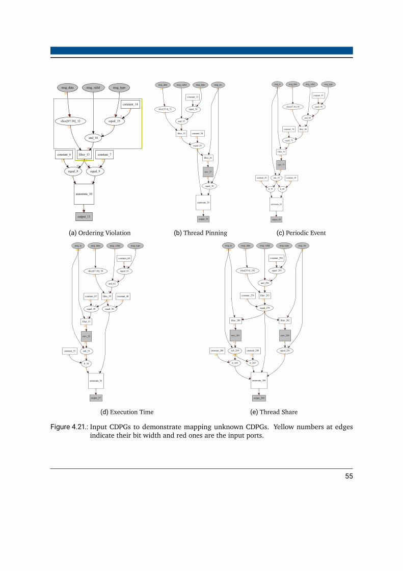
msg_valid msg_type
and_16
1
1
equal_15
0
4
constant_14
1
4
0
1
filter_13
0
1
msg_data
slice[67:36]_12
0
68
1
32
equal_8
0
32
equal_9
0
32
constant_6
1
32
automata_10
0
1
constant_7
1
32
1
1
output_11
0
3
(a) Ordering Violation
msg_valid msg_type
and_35
1
1
equal_34
0
4
msg_src
constant_33
1
4
0
1
filter_32
0
1
msg_data
slice[35:4]_31
0
68
1
32
equal_250
32
constant_24
1
32
filter_26
1
8
equal_30
1
8
0
1
automata_28
0
1
mrv_27
0
8
0
8
1
1
output_29
0
3
(b) Thread Pinning
constant_82
lt_790
48
msg_valid msg_type
and_89
1
1
equal_88
0
4
constant_87
1
4
0
1
filter_86
0
1
msg_data
slice[67:36]_85
0
68
1
32
equal_750
32
msg_ts
filter_76
1
48
sub_78
0
48
constant_81
lt_801
48
constant_74
1
32
0
1
mrv_77
0
48
1
48
1
48
0
48
automata_83
0
1
1
1
output_84
0
3
(c) Periodic Event
constant_47
equal_49
1
32
constant_48
equal_501
32
constant_55
lt_541
48
msg_valid msg_type
and_62
1
1
equal_61
0
4
constant_60
1
4
0
1
filter_59
0
1
msg_data
slice[67:36]_58
0
68
1
32
0
32
0
32
automata_56
0
1
filter_51
0
1
msg_ts
1
48
sub_53
0
48
mrv_52
0
48
1
48
0
48
1
1
output_57
0
3
(d) Execution Time
constant_286
lt_2850
48
constant_278
equal_2791
32
msg_src
filter_282
1
8
equal_291
1
8
msg_valid msg_type
and_296
1
1
equal_295
0
4
constant_294
1
4
0
1
filter_293
0
1
msg_data
slice[35:4]_292
0
68
1
32
0
32
0
1
filter_2800
1
automata_289
3
1
mrv_283
0
8
0
8
2
1
msg_ts
1
48
sub_284
0
48
mrv_281
0
48
constant_288
lt_287
1
48
1
48
1
48
0
48
0
1
1
1
output_290
0
3
(e) Thread Share
Figure 4.21.: Input CDPGs to demonstrate mapping unknown CDPGs. Yellow numbers at edgesindicate their bit width and red ones are the input ports.
55

was performed using the Bron-Kerbosch clique finder. The resulting CDPG has the samestructure in all five cases but it is constructed from only four input CDPGs.
In Figures 4.22 (b) and (e) the multi edge matching of the ILP mapping algorithm canbe seen. In both cases a single comparator with a constant is sufficient but the mapperfinds the solution using both comparators first. This is not wrong or a drawback as everycomplete solution is of equal value. Figure 4.22f shows the alternative generated by thebipartite mapping algorithm. It took 1.3ms on average to map the remaining CDPG usingthe ILP mapper and 0.5ms for the bipartite mapper. The maximum runtimes were alwaysless than double the average in both cases.
56

constant_115
equal_116
1
32
msg_valid msg_type
and_243
1
1
equal_242
0
4
msg_src
constant_241
1
4
0
1
filter_240
0
1
msg_data
slice[67:36]_239
0
68
slice[35:4]_249
0
68
1
32
0
32
equal_930
32
filter_1170
1
automata_124
3
1
filter_1340
1
constant_122
lt_1211
48
constant_123
lt_120
0
48
msg_ts
1
48
sub_119
0
48
mrv_118
0
48
1
48
0
48
1
48
1
1
0
1
output_125
0
3
constant_91
1
32
2
1
1
8
equal_138
1
8
1
32
mrv_135
0
8
0
8
4
1
(a) Ordering Violation
constant_115
equal_116
1
32
msg_valid msg_type
and_193
1
1
equal_192
0
4
msg_src
constant_191
1
4
0
1
filter_190
0
1
msg_data
slice[67:36]_189
0
68
slice[35:4]_199
0
68
1
32
0
32
equal_930
32
filter_1170
1
automata_124
3
1
filter_1050
1
constant_122
lt_1211
48
constant_123
lt_120
0
48
msg_ts
1
48
sub_119
0
48
mrv_118
0
48
1
48
0
48
1
48
1
1
0
1
output_125
0
3
constant_91
1
32
4
1
1
8
equal_114
1
8
1
32
mrv_106
0
8
0
8
2
1
(b) Thread Pinning
msg_ts msg_data
filter_94
1
48
sub_96
0
48
msg_src
filter_134
1
8
equal_138
1
8
msg_valid
slice[67:36]_139
0
68
slice[35:4]_144
0
68
msg_type
and_143
1
1
equal_142
0
4
constant_90
equal_92
1
32
constant_91
equal_93
1
32
constant_141
1
4
0
1
filter_140
0
1
1
32
0
32
0
32
0
1
automata_99
4
1
0
1
constant_98
lt_971
48
0
1
3
1
mrv_95
0
48
1
48
0
48
lt_1081
48
0
1
output_100
0
3
1
32
mrv_135
0
8
0
8
1
1
constant_109
0
48
2
1
(c) Periodic Event
constant_115
equal_116
1
32
msg_valid msg_type
and_168
1
1
equal_167
0
4
msg_src
constant_166
1
4
0
1
filter_165
0
1
msg_data
slice[67:36]_164
0
68
slice[35:4]_169
0
68
1
32
0
32
equal_1290
32
filter_1170
1
automata_124
3
1
filter_1340
1
constant_122
lt_121
1
48
constant_123
lt_1200
48
msg_ts
1
48
sub_119
0
48
mrv_118
0
48
1
48
0
48
1
48
1
1
0
1
output_125
0
3
1
8
equal_138
1
8
1
32
mrv_135
0
8
0
8
2
1
constant_127
1
32
4
1
(d) Execution Time
constant_115
equal_116
1
32
msg_valid msg_type
and_218
1
1
equal_217
0
4
msg_src
constant_216
1
4
0
1
filter_215
0
1
msg_data
slice[67:36]_214
0
68
slice[35:4]_224
0
68
1
32
0
32
equal_930
32
filter_1170
1
automata_124
3
1
filter_1340
1
constant_122
lt_1211
48
constant_123
lt_120
0
48
msg_ts
1
48
sub_119
0
48
mrv_118
0
48
1
48
0
48
1
48
1
1
0
1
output_125
0
3
constant_91
1
32
2
1
1
8
equal_138
1
8
1
32
mrv_135
0
8
0
8
4
1
(e) Thread Share
constant_36
equal_38
1
32
msg_valid msg_type
and_153
1
1
equal_152
0
4
msg_src
constant_151
1
4
0
1
filter_150
0
1
msg_data
slice[67:36]_149
0
68
slice[35:4]_154
0
68
1
32
0
32
equal_39
0
32
automata_400
1
constant_37
1
32
1
1
filter_440
1
filter_270
1
output_41
0
3
1
32
1
8
equal_48
1
8
mrv_45
0
8
0
8
2
1
constant_33
lt_300
48
msg_ts
1
48
sub_29
0
48
constant_32
lt_31
1
48
mrv_28
0
48
1
48
1
48
0
48
3
1
4
1
(f) Alternative mapping to (e)
Figure 4.22.: Mapping the CDPG that was not contained in the input set to create the merged CDPG.In all cases a valid mapping result can be obtained.
57

4.6. Results
This chapter reviews the applicability of the presented method on real world applications.For that, four possible monitors were specified using TeSSLa. Their characteristics are notcompletely orthogonal but they are also not congruent to each other. The implementedmonitors report an error in case of
1. …a shared ring buffer was read more often than written (Race Condition) or themaximum number of elements in the buffer is exceeded (Buffer Overflow).
2. …a producer task is stopped before the consumer task is stopped (Ordering Violation).
3. …any of a set of functions exceeds a given upper execution time (Timing Constraints).
4. …the complexity bound for an algorithm is exceeded (Complexity Bound).
In the appendix in Listings A.1-A.4 the corresponding TeSSLa descriptions can be found.
4.6.1. Resource Utilization
When the monitor system is synthesized, the FPGA utilization strongly depends on thenumber of implemented monitors and their size. The resource utilization for all fourscenarios and their merged EP is given in Table 4.2. It shows that the merged EP is smallerthan just the sum of its contributing monitors, including the resources for the configurationinterface and the CEs. The savings are not huge but as stated in the motivation the majorgoal of monitor merging is the reconfigurability. Nevertheless, compared to the TimingConstraint monitor, the implemented EP uses 64% more LUTs and 42% more registers.The number of registers increases due to the configuration and constant registers while theincreased number of LUTs is partially caused by the multiplexers.
The target FPGA for synthesis is a Virtex-7 XC7VX485T containing 485,768 LUTs, 607,200registers, and 1,030 BRAMs of 36 kBit. It can be used completely for the RV platform becausea smaller version of the trace reconstruction is performed on the Zynq’s FPGA fabric. The EVwas accessed on the Virtex’ IOs. According to these numbers, the merged monitor could beimplemented around 300 times. Experiments have shown that at least 256 merged EPs fiton the FPGA when the configuration and communication infrastructure is included. A laterimplementation for production will not consist of two separate FPGAs. The reconstructionand the analysis have to be implemented on the same chip. Thereby, the resources availablefor RV will be less.
58
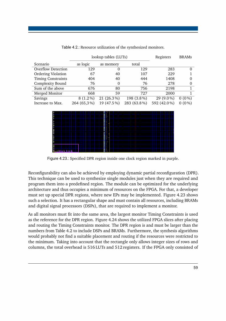
Table 4.2.: Resource utilization of the synthesized monitors.
lookup tables (LUTs) Registers BRAMs
Scenario as logic as memory totalOverflow Detection 129 0 129 283 0Ordering Violation 67 40 107 229 1Timing Constraints 404 40 444 1408 0Complexity Bound 76 0 76 278 0Sum of the above 676 80 756 2198 1Merged Monitor 668 59 727 2000 1Savings 8 (1.2%) 21 (26.3%) 198 (3.8%) 29 (9.0%) 0 (0%)Increase to Max. 264 (65,3%) 19 (47.5%) 283 (63.8%) 592 (42.0%) 0 (0%)
Figure 4.23.: Specified DPR region inside one clock region marked in purple.
Reconfigurability can also be achieved by employing dynamic partial reconfiguration (DPR).This technique can be used to synthesize single modules just when they are required andprogram them into a predefined region. The module can be optimized for the underlyingarchitecture and thus occupies a minimum of resources on the FPGA. For that, a developermust set up special DPR regions, where new EPs may be implemented. Figure 4.23 showssuch a selection. It has a rectangular shape and must contain all resources, including BRAMsand digital signal processors (DSPs), that are required to implement a monitor.
As all monitors must fit into the same area, the largest monitor Timing Constraints is usedas the reference for the DPR region. Figure 4.24 shows the utilized FPGA slices after placingand routing the Timing Constraints monitor. The DPR region is and must be larger than thenumbers from Table 4.2 to include DSPs and BRAMs. Furthermore, the synthesis algorithmswould probably not find a suitable placement and routing if the resources were restricted tothe minimum. Taking into account that the rectangle only allows integer sizes of rows andcolumns, the total overhead is 516 LUTs and 512 registers. If the FPGA only consisted of
59

Figure 4.24.: Resource utilization of the Timing Constraint monitor inside a DPR region. Usedslices are marked in turquoise and the module’s IO in white.
those blocks, the area on the Virtex-7 XC7VX485T would have allowed to mark roughly 350blocks, not yet including any communication infrastructure.
4.6.2. Runtime Comparison
In the merging process the CG can become huge. The first merging step produces a graphcontaining 445 compatibility nodes and 78526 compatibility edges and represents thelargest problem. The other two compatibility graphs have around 300 nodes and 40,000edges. Finding the exact maximum clique as the optimum reference, using the algorithmfrom Bron and Kerbosch [38], exceeded the servers memory capabilites of 128GB, whichmakes it intractable. Table 4.3 shows that the time for solving all of the three maximumclique searches is within 1.33 seconds. This proves that the heuristic can cope with problemsizes that occur in real applications. The code generation takes less than a second butdepending on the CDPG size it might increase. Code generation also includes modification
Table 4.3.: Tool flow time consumption.
Step Time/msMerging 1333Code generation 450-700Mapping 350 - 750Download < 1
60

Table 4.4.: Times to map the monitors onto the merged monitor.
Bipartite Graph GLPK Solver
Total Mapping Total Mapping
Scenario t/µs t/µs σ/µs t/µs t/µs σ/µsBuffer Overflow 162476.9 6048.5 760.8 213568.4 16325.1 941.4Ordering Violation 171664.3 13153.0 784.8 267961.3 49020.1 1501.4Timing Constraints 221265.6 34365.6 1785.7 321542.3 86153.2 1203.5Complexity Bound 158760.8 4394.0 392.4 209017.4 13431.1 403.0
and optimization of the graph. Optimization is performed by shifting registers from operationinputs to outputs when bits can be saved. Both of these steps only have to be done onceand are not intended to be run frequently.
In contrast to the merging, the mapping and downloading will probably be executed manytimes in short intervals. A time of less than one second to reconfigure a monitor with a newfunctionality is an acceptable turnaround time for RV. Table 4.4 shows the overall runtimesof 1000 mapping runs for every scenario using both the bipartite and the ILP mappingmethod. Additionally, for the pure mapping algorithm a variance is calculated.
To compare the mapping against the DPR variant, the four scenarios where synthesizedand implemented in the DPR region. Table 4.5 shows that the runtimes for synthesis,placement, and routing are in close range to 70 s, which is most likely due to the smallarea constraints. This does not yet include the time for generating a partial bitstream anddownloading it to the FPGA. The runtime reconfigurable approach clearly outperformsthis, as the mapping and the downloading times from Table 4.4 are always less than onesecond. The reconfiguration step has to be done every time a single operation or even only
Table 4.5.: Out-of-context synthesis times for a DPR setup.
Scenario Synthesis [s] Place [s] Route [s] Total [s]Buffer Overflow 32 10 28 70Ordering Violation 33 10 28 71Timing Constraints 32 11 25 68Complexity Bound 32 10 29 71
61

a value in the CDPG changes. Hence, compared to a turnaround time of 70 s for the DPR,the presented solution is more acceptable. Beyond that, the DPR toolflow requires skilledand experienced hardware developers.
62

4.7. Tool Flow
The tool flow is divided into two major parts - generating the RV platform and programmingit to activate monitors. The first one is clearly the more time-consuming one as it consists ofthe monitor merging and later synthesizing the actual hardware. As a consequence this stepis executed as rarely as possible, only once in the best case. Afterwards, the programmingcan be done frequently whenever the assertion for a monitor changes. It is usually performedwithin seconds.
4.7.1. Generating the Runtime Verification Platform
Figure 4.25 shows the process from specifying monitors to programming the RV platformon the FPGA. In the beginning the user formulates a set of assertions/monitors he wants tovalidate. These are then compiled into CDPGs using the TeSSLa compiler and afterwardsmerged into a configurable CDPG. It is also possible to divide the assertions into subsetsand generate multiple different configurable CDPGs. Thus, an apriori grouping, e.g. by thenature of the assertions, can be performed. The resulting CDPG(s) is stored in a new file.When a new monitor needs to be added later this enables an incremental update of theconfigurable CDPG. It is not necessary to merge all previously specified monitors again.
Once the user is confident that he formulated enough (prototypical) monitors he mustspecify how many shall be available in the RV platform. The platform description shown inListing 4.4 is an extensible markup language (XML) file that contains information about the(merged) monitors to be implemented and their addresses. If required, a priority for the
monitor set 1
monitor set 2
merged monitor 1
merged monitor 2
000110110110001001001001000110100100110010101100010001111001101010111001100110100010011001
bitstream
static componentsalways@(posedge clk) begin if(rst) begin reg_a <= 32'h0000_0000; reg_b <= 8'hF; end else begin reg_a <= reg_a + input_n; reg_b <= reg_a[7:0]; endend
superposition
superposition
<?xml version="1.0" encoding="<processing_system> <processor> <type>event_proc</type> <address>0</address> <priority>0</priority> </processor></processing_system>
system description
codegeneration
always@(posedge clk) begin if(rst) begin reg_a <= 32'h0000_0000; reg_b <= 8'hF; end else begin reg_a <= reg_a + input_n; reg_b <= reg_a[7:0]; endend
Verilog modules
configurationinformation
synthesis
Figure 4.25.: Tool flow to generate the runtime verification platform.
63
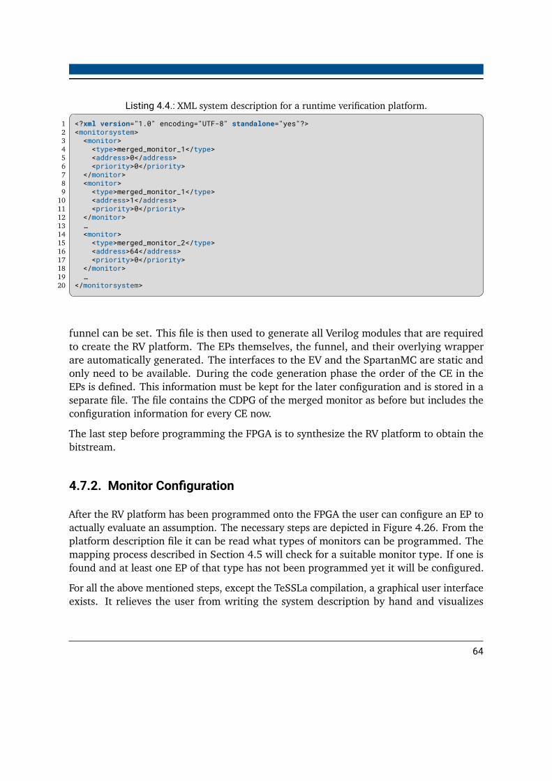
Listing 4.4.: XML system description for a runtime verification platform.
1 <?xml version="1.0" encoding="UTF-8" standalone="yes"?>2 <monitorsystem>3 <monitor>4 <type>merged_monitor_1</type>5 <address>0</address>6 <priority>0</priority>7 </monitor>8 <monitor>9 <type>merged_monitor_1</type>
10 <address>1</address>11 <priority>0</priority>12 </monitor>13 …14 <monitor>15 <type>merged_monitor_2</type>16 <address>64</address>17 <priority>0</priority>18 </monitor>19 …20 </monitorsystem>
funnel can be set. This file is then used to generate all Verilog modules that are requiredto create the RV platform. The EPs themselves, the funnel, and their overlying wrapperare automatically generated. The interfaces to the EV and the SpartanMC are static andonly need to be available. During the code generation phase the order of the CE in theEPs is defined. This information must be kept for the later configuration and is stored in aseparate file. The file contains the CDPG of the merged monitor as before but includes theconfiguration information for every CE now.
The last step before programming the FPGA is to synthesize the RV platform to obtain thebitstream.
4.7.2. Monitor Configuration
After the RV platform has been programmed onto the FPGA the user can configure an EP toactually evaluate an assumption. The necessary steps are depicted in Figure 4.26. From theplatform description file it can be read what types of monitors can be programmed. Themapping process described in Section 4.5 will check for a suitable monitor type. If one isfound and at least one EP of that type has not been programmed yet it will be configured.
For all the above mentioned steps, except the TeSSLa compilation, a graphical user interfaceexists. It relieves the user from writing the system description by hand and visualizes
64
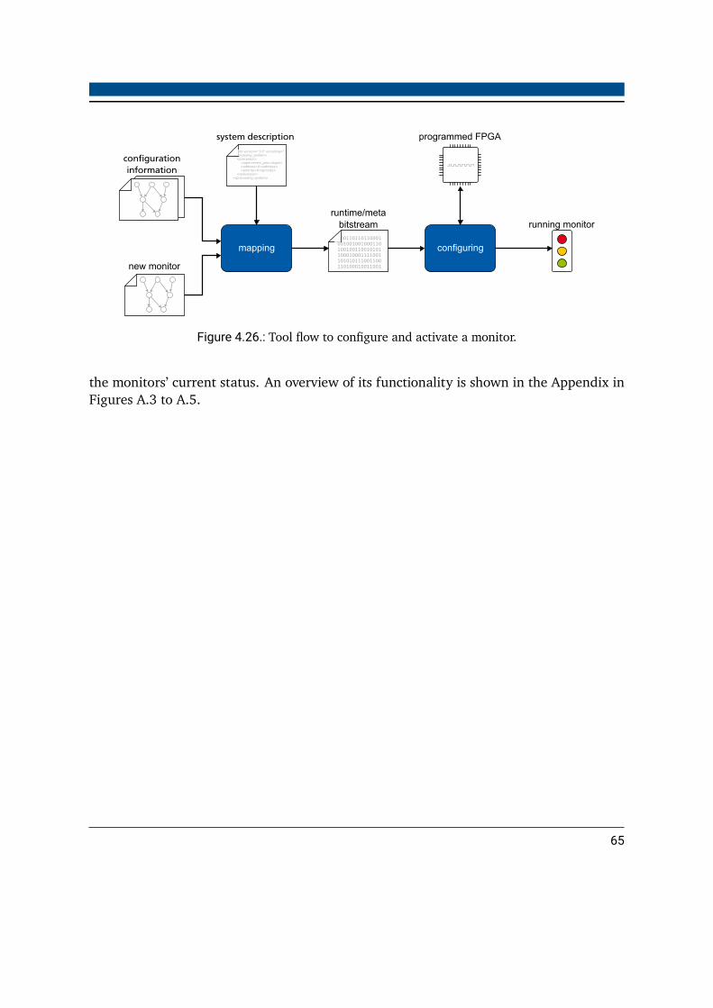
configuration
information
new monitor
<?xml version="1.0" encoding="<processing_system> <processor> <type>event_proc</type> <address>0</address> <priority>0</priority> </processor></processing_system>
system description
mapping configuring
running monitorruntime/meta
bitstream000110110110001001001001000110100100110010101100010001111001101010111001100110100010011001
programmed FPGA
Figure 4.26.: Tool flow to configure and activate a monitor.
the monitors’ current status. An overview of its functionality is shown in the Appendix inFigures A.3 to A.5.
65

4.8. Conclusion and Outlook
The runtime reconfiguration approach has shown to perform well for RV. The user onlyneeds to specify his assertions and can generate a complete hardware system to analyzehis embedded software. With some care even assertions that are similar to the previouslyspecified ones can be mapped afterwards without re-synthesizing the whole system. Thechosen mapping technique using bipartite graphs has turned out to be extremely fast for thedemonstrated real world scenarios. Turnaround times from specifying an assertion until itis configured onto the RV platform are in the order of seconds. This makes the procedureapplicable for interactive working in rapidly changing applications.
In both the merging as well as in the mapping procedure there are still optimizationsconceivable. To obtain a better result in terms of required resources, structural optimizationscan be applied before a CDPG is transformed into a Verilog module. Arithmetic as well aslogical operations that have high bit widths can be implemented in DSP blocks. Especiallyfused operations like multiply-accumulate benefit from their hardwired logic and internalpipelining. Furthermore, DSPs allow - once they are used in the design - a number ofoperations that can be configured during runtime although they were not designated in anyof the CDPGs.
To increase the degree of generality and allow more problems to be mapped onto an EP,two enhancements are possible. The first is applied even before the merging phase andregards the order of operations in the CDPGs. If it is not necessary that operations stay inexact order, these can be permuted into a canonical form. This makes the CDPGs’ structuremore independent of how the user specifies his assertions and automatically introducesmore commonalities. The second option is to make use of neutral elements for operations.When for example an addition or subtraction with a constant is in a path of interest, settingthe constant to zero will effectively bypass it. The same holds true for multiplications withone. This virtually increases the amount of edges between operations in the synthesized EP.
Another topic that has to be covered to further increase the user experience is the detectionof (un)similar DPGs. Until now it is up to the user to define sets of problems that are worthmerging. When he chooses two assertions that have close to no commonalities the benefitof merging is rather small. He can then basically configure only those two. A metric thatautomatically bundles very similar CDPGs together has yet to be implemented.
66

5. Resource Optimization for High LevelSynthesis
5.1. Problem Description
FPGAs have become a very powerful platform for implementing digital systems. They havegrown so far that complete micro processor designs fit into them which are then calledsoft cores. Popular and commercially available are e.g. the Microblaze from Xilinx [39] orthe NIOS II from Altera/Intel [40]. Depending on the users needs there are variants thattarget a higher performance or alternatively better resource efficiency. What nearly all softcores have in common is their extendability. Custom interlectual property (IP) cores can beflanged to increase connectivity or add coprocessors.
When a time-consuming task is executed repetitively, it is reasonable to create a dedicatedhardware unit for it. Not executing the task in software but in hardware can firstly reducethe processing load of the soft core and secondly speed up its execution. Even if the processordoes not have other tasks to do, the speedup itself may already be worth it.
Depending on the size of a hardware accelerator and the FPGA they can consume a nonnegligible amount of available resources. Sophisticated resource and register allocationand binding algorithms can reduce this stress. Another potential can be exploited whenmultiple accelerators are implemented. As long as their execution times are disjoint, theresources of a DP can be reused in another one’s. This type of resource optimization cannotbe performed by the synthesis tools themselves. They only have notion of the temporalbehavior on the register transfer level (RTL) and not the controlling software.
The hardware accelerators that are generated by HLS tools usually follow the DP + CUscheme that was introduced in Section 2.1. This approach makes the accelerators suitablefor merging using the approach presented in Chapter 3. The extent to which and howmany resources can be shared depends not only on the similarity of the DP but also on theresource binding.
67

UART
SpartanMCCore
Memory AcceleratorI2C SPI
Peripheral Bus
Memory Bus
Figure 5.1.: SpartanMC softcore connected to peripherals including a hardware accelerator withdirect memory access.
5.2. Hardware Accelerators
The hardware accelerators used in this chapter are generated by a plugin for the GCC thatwas initially developed by Vogt et. al [41] and continued in [42], [43], and [44]. By now, itis called PIRANHA which stands for Plugin for Intermediate Representation Analysis andHardware Acceleration. In this work it targets the SpartanMC SoC-Kit [29] instead of aZynq [24]. Following, the steps to create a hardware accelerator for a SpartanMC projectare presented.
Figure 5.1 shows the basic structure of the SpartanMC SoC. At first, there is the soft core itselfand its main memory. Most peripherals are connected to it via peripheral bus. Peripheralsthat have to transfer high amounts of data, such as the hardware accelerator, additionallyhave direct memory access (DMA) to the processor’s memory. This structure is given andnot modified in this work. The SpartanMC has one characteristic that differentiates it fromother soft cores. In order to fully use the resources like BRAMs and DSPs on Xilinx FPGAs,it has an 18 bit architecture. Thus, the bitwidths of data and operations is not 8 or 16 bitsbut 9 or 18 bits respectively.
68

5.2.1. Tool Flow
The toolflow for creating a SpartanMC system that contains a hardware accelerator isstraight forward and can be summarized as follows:
1. Set up a SpartanMC project.
2. Build the firmware and the accelerator.
3. Synthesize the design.
4. Program the FPGA.
System Setup The SpartanMC project is set up by selecting a target platform and thesynthesis toolchain, in this case the Nexys Video [45] board and Vivado [46]. The targetfrequency of the processor is set to 70MHz which is the maximum for the SpartanMC onthe Nexys Video at this point. It is also the frequency for the accelerator because setupswith multiple DMA clock domains are not supported. A universal asynchronous receiver &transmitter (UART) module and the accelerator itself are the only peripherals connected tothe SpartanMC. Together with the accelerator a cache system can be installed to increasethe number of memory ports for parallel memory access. However, the setup used in thiswork only uses a single memory port.
Firmware Compilation Building the firmware includes the source code analysis for accel-erator extraction. Like other HLS tools PIRANHA analyzes and identifies loops, which maybe nested, that are worth accelerating. These loops, also called kernels, are then scheduled,optimized, and transformed into Verilog modules. They are encapsulated in an acceleratorperipheral that can be accessed from the firmware running on the soft core. The firmwareitself is patched so that the loop is not executed in software any more. Instead of thesoftware routine, a function that configures and starts the accelerator is called. It includestransfering live-in variables to the accelerator, starting it and waiting for it to finish, and inthe end transfer back live-out variables. The internal compile flow can be comprehended inFigure 5.2.
Different schedulers and optimization options can be chosen in PIRANHA. A rotationscheduler is used to generate kernel accelerators that benefit from iteration level parallelismby overlapping them. Furthermore, chaining and speculation, both techniques to enhancethe speedup, are activated. These are explained later in this chapter.
69
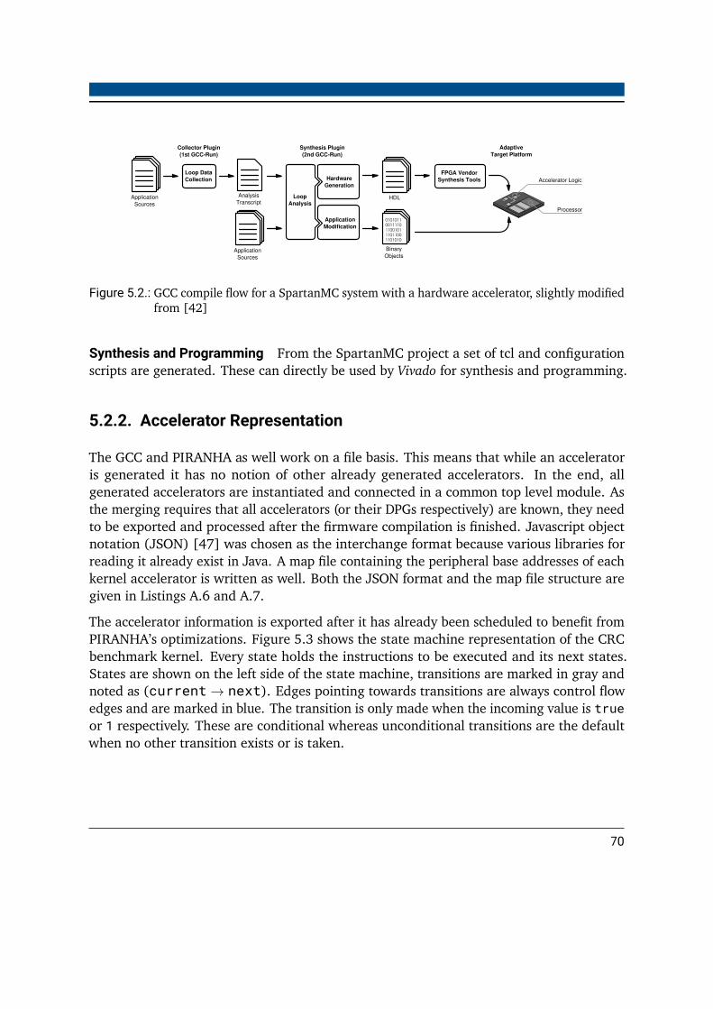
HardwareGeneration
0011110110010111011001101010
0101011
Loop DataCollection
Application
Sources
LoopAnalysis
Application
Modification
FPGA VendorSynthesis Tools
AnalysisTranscript
Processor
HDL
Accelerator Logic
Collector Plugin
(1st GCC-Run)
Synthesis Plugin
(2nd GCC-Run)
AdaptiveTarget Platform
Binary
Objects
ApplicationSources
Figure 5.2.: GCC compile flow for a SpartanMC system with a hardware accelerator, slightly modifiedfrom [42]
Synthesis and Programming From the SpartanMC project a set of tcl and configurationscripts are generated. These can directly be used by Vivado for synthesis and programming.
5.2.2. Accelerator Representation
The GCC and PIRANHA as well work on a file basis. This means that while an acceleratoris generated it has no notion of other already generated accelerators. In the end, allgenerated accelerators are instantiated and connected in a common top level module. Asthe merging requires that all accelerators (or their DPGs respectively) are known, they needto be exported and processed after the firmware compilation is finished. Javascript objectnotation (JSON) [47] was chosen as the interchange format because various libraries forreading it already exist in Java. A map file containing the peripheral base addresses of eachkernel accelerator is written as well. Both the JSON format and the map file structure aregiven in Listings A.6 and A.7.
The accelerator information is exported after it has already been scheduled to benefit fromPIRANHA’s optimizations. Figure 5.3 shows the state machine representation of the CRCbenchmark kernel. Every state holds the instructions to be executed and its next states.States are shown on the left side of the state machine, transitions are marked in gray andnoted as (current→ next). Edges pointing towards transitions are always control flowedges and are marked in blue. The transition is only made when the incoming value is trueor 1 respectively. These are conditional whereas unconditional transitions are the defaultwhen no other transition exists or is taken.
70

State 0
State 1
0->1
State 2
1->2
State 3
2->3
State 4
3->4
State 5
4->5
State 6
5->6
State 7
6->7
State 8
7->8
State 9
8->9
State 10
9->10
State 11
10->11
State 12
11->12
State 13
12->13
State 14
13->14
State 15
State 16
15->10
State 17
16->17
State 18
17->18
State 19
State 20
19->0
20->1
!=(u)hw_tmp_4294965_000
18->20
[1]
0~(u)
hw_tmp_4294958_000
[1]0
:=(u)tmp_4_004
<<(u)tmp_5_005
[18]
0
:=(s)reg_37_037
^(u)reg_19_019
[18]
1
:=(u)tmp_13_013_cc_0
[18]
1
:=(u)ivtmp_16_27_027
:=(u)tmp_15_015
[18]0
+(u)ivtmp_16_25_025
[18]
0
2->2 SA1 id: 1(u)
&(u)tmp_7_007
[18]
0
:=(u)ivtmp_16_27_027
[18]
0
[18]
0
:=(u)reg_37_037
[18]
1
!=(u)hw_tmp_4294967_000
:=(u)reg_12_012
@False
:=(u)reg_12_012
@True
^(u)reg_22_022
[18]
0
!=(u)hw_tmp_4294966_000
14->15
[1]
0~(u)
hw_tmp_4294959_000
[1]
0
[18]0
:=(u)ivtmp_31_031
-(u)ivtmp_30_030
[18]
0
&(u)reg_23_023
[18]
0
[18]
0
:=(u)reg_36_036
[18]
0
:=(u)reg_33_033
[18]
0
&(u)tmp_8_008
[18]
0
<<(u)tmp_41_041
[18]
0
[18]
0
[18]
0
:=(u)ivtmp_31_031
[18]
0
:=(u)reg_36_036
[18]0
[18]
0
[18]
0
18->19[1]0
[18]
0
[18]
0
[18]
0
:=(s)tmp_6_006
[18]0
[18]
0
3->3 RD1 id: 1(u)tmp_3_003
[9]0
[18]
0
[18]
0
14->16
[1]
0
[18]
0
reg_33_033
[18]
0
:=(s)exit_bb_idx_000
exit_bb_idx_000
[18]
0
ivtmp_16_16_016
[18]
0
tmp_13_013
[18]
0
mem_ack
[1]
0 @True
[1]
0
18'sh00000
[18]0
18'h0ff00
[18]
1
18'h08000
[18]
1
18'h00001
[18]
1
18'h00001
[18]
1
18'h0ffff
[18]
1
18'h00000
[18]
1
18'sh00008
[18]
0
18'h00000
[18]
1
18'h00008
[18]
1
18'h01021
[18]
1
18'h00001
[18]
1
18'h00008
[18]
0
Figure 5.3.: State machine representation of the CRC-benchmark’s kernel. The states and defaulttransitions are located on the left. Blue edges indicate control flow. All other edges aredata flow.
71
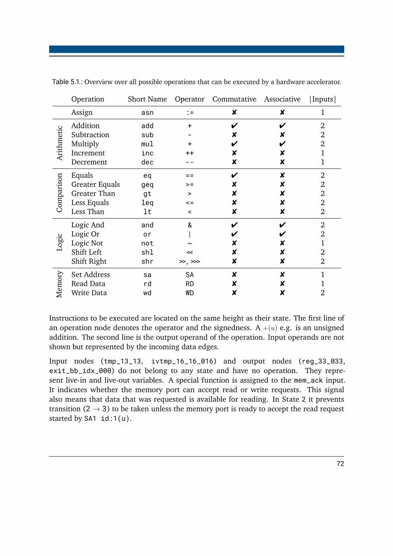
Table 5.1.: Overview over all possible operations that can be executed by a hardware accelerator.
Operation Short Name Operator Commutative Associative |Inputs|
Assign asn := 8 8 1
Arith
metic Addition add + 4 4 2
Subtraction sub - 8 8 2Multiply mul * 4 4 2Increment inc ++ 8 8 1Decrement dec -- 8 8 1
Compa
rison Equals eq == 4 8 2
Greater Equals geq >= 8 8 2Greater Than gt > 8 8 2Less Equals leq <= 8 8 2Less Than lt < 8 8 2
Logic
Logic And and & 4 4 2Logic Or or | 4 4 2Logic Not not ~ 8 8 1Shift Left shl << 8 8 2Shift Right shr >>, >>> 8 8 2
Mem
ory Set Address sa SA 8 8 1
Read Data rd RD 8 8 1Write Data wd WD 8 8 2
Instructions to be executed are located on the same height as their state. The first line ofan operation node denotes the operator and the signedness. A +(u) e.g. is an unsignedaddition. The second line is the output operand of the operation. Input operands are notshown but represented by the incoming data edges.
Input nodes (tmp_13_13, ivtmp_16_16_016) and output nodes (reg_33_033,exit_bb_idx_000) do not belong to any state and have no operation. They repre-sent live-in and live-out variables. A special function is assigned to the mem_ack input.It indicates whether the memory port can accept read or write requests. This signalalso means that data that was requested is available for reading. In State 2 it preventstransition (2→ 3) to be taken unless the memory port is ready to accept the read requeststarted by SA1 id:1(u).
72
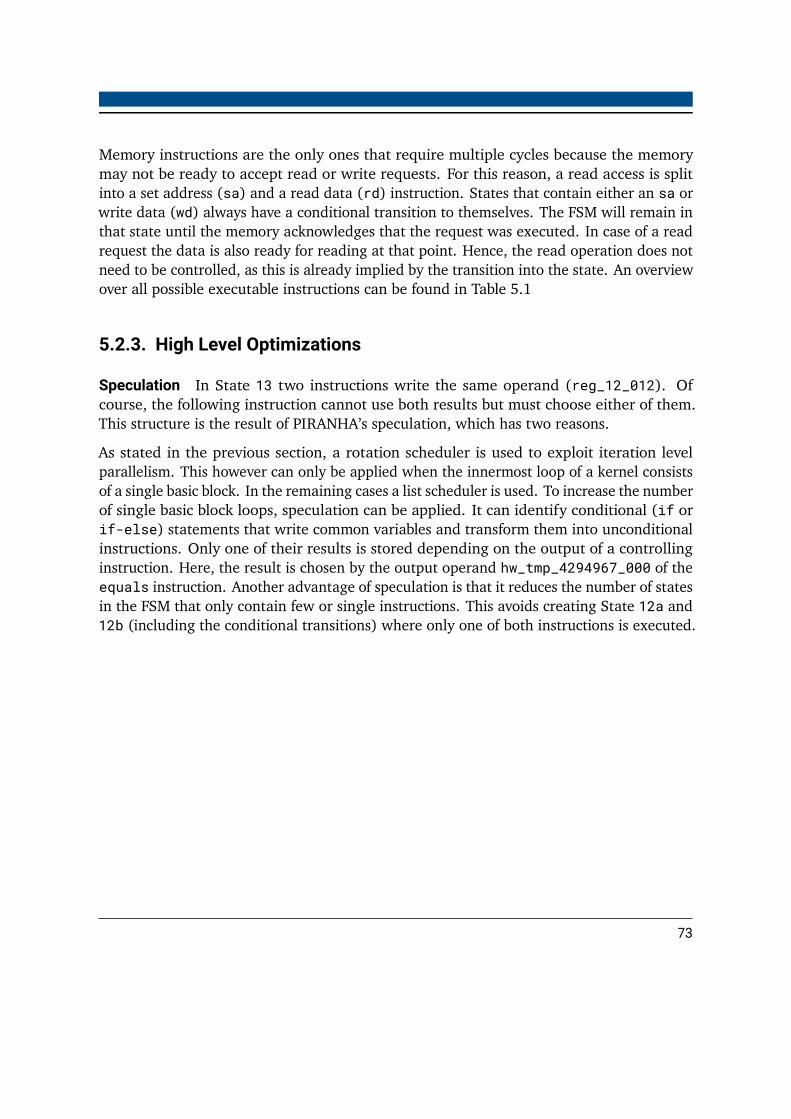
Memory instructions are the only ones that require multiple cycles because the memorymay not be ready to accept read or write requests. For this reason, a read access is splitinto a set address (sa) and a read data (rd) instruction. States that contain either an sa orwrite data (wd) always have a conditional transition to themselves. The FSM will remain inthat state until the memory acknowledges that the request was executed. In case of a readrequest the data is also ready for reading at that point. Hence, the read operation does notneed to be controlled, as this is already implied by the transition into the state. An overviewover all possible executable instructions can be found in Table 5.1
5.2.3. High Level Optimizations
Speculation In State 13 two instructions write the same operand (reg_12_012). Ofcourse, the following instruction cannot use both results but must choose either of them.This structure is the result of PIRANHA’s speculation, which has two reasons.
As stated in the previous section, a rotation scheduler is used to exploit iteration levelparallelism. This however can only be applied when the innermost loop of a kernel consistsof a single basic block. In the remaining cases a list scheduler is used. To increase the numberof single basic block loops, speculation can be applied. It can identify conditional (if orif-else) statements that write common variables and transform them into unconditionalinstructions. Only one of their results is stored depending on the output of a controllinginstruction. Here, the result is chosen by the output operand hw_tmp_4294967_000 of theequals instruction. Another advantage of speculation is that it reduces the number of statesin the FSM that only contain few or single instructions. This avoids creating State 12a and12b (including the conditional transitions) where only one of both instructions is executed.
73
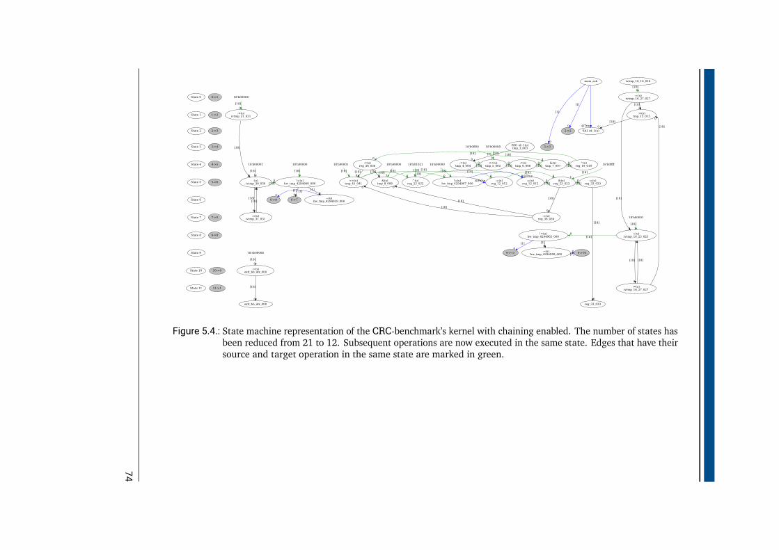
State 0
State 1
0->1
State 2
1->2
State 3
2->3
State 4
3->4
State 5
4->5
State 6
5->6
State 7
State 8
7->5
State 9
8->9
State 10
State 11
10->0
11->1
-(u)ivtmp_30_030
!=(u)hw_tmp_4294966_000[18]
0
:=(u)ivtmp_31_031
[18]
0
:=(u)reg_33_033
reg_33_033
6->7
[1]
0~(u)
hw_tmp_4294959_000
[1]0
^(u)reg_22_022
:=(u)reg_12_012
[18]
0
<<(u)tmp_41_041
[18]0
:=(u)reg_12_012
[18]
0
!=(u)hw_tmp_4294967_000
@True
@False &(u)reg_23_023 [18]
0
:=(u)reg_36_036
[18]
0
&(u)tmp_8_008
[18]
0
[18]0
[18]0
6->8
[1]0
[18]
0
[18]
0
[18]
0
:=(u)ivtmp_16_27_027
:=(u)tmp_15_015
[18]0
+(u)ivtmp_16_25_025
[18]
0
2->2 SA1 id: 1(u)
:=(s)tmp_6_006
&(u)tmp_7_007[18]
0:=(u)reg_36_036
[18]0
[18]0
^(u)reg_19_019[18]
0<<(u)tmp_5_005 [18]
0
[18]
0
:=(u)tmp_4_004 [18]
0
:=(u)ivtmp_31_031
[18]
0
RD1 id: 1(u)tmp_3_003
[9]
0
9->10~(u)hw_tmp_4294958_000 [1]
09->11
!=(u)hw_tmp_4294965_000
[1]0
[1]
0
:=(u)ivtmp_16_27_027
[18]
0
[18]
0
ivtmp_16_16_016
[18]0
mem_ack
[1]
0 @True[18]
0
3->3
[18]
1
18'h01021
[18]1
18'h00008
[18]
0
18'h00001
[18]
1
18'h08000
[18]
1
18'h0ffff
:=(s)exit_bb_idx_000
exit_bb_idx_000
[18]
0
ff00
[18]
1
18'h00001
[18]
1
18'h00000
[18]
1
18'h00008
[18]
1
18'h00001
[18]
1
Figure 5.4.: State machine representation of the CRC-benchmark’s kernel with chaining enabled. The number of states hasbeen reduced from 21 to 12. Subsequent operations are now executed in the same state. Edges that have theirsource and target operation in the same state are marked in green.
74

Chaining PIRANHA also supports chaining as an option to improve speedup. Withoutchaining, an instruction that depends on another is never executed in the same state orcycle. As gate level execution times strongly depend on the bit width and their type of theoperation, instructions may be executed in the same cycle as their predecessors withoutviolating timing constraints. Figure 5.4 again shows the CRC kernel’s state machine butthis time with chaining enabled. The instructions from States 4 to 9 are now all in State 4and instructions from States 10 to 13 have moved to State 5.
Table 5.2 shows the positive effect of chaining. As expected, the number of registers stronglydecreases (by ≈29% on average) because many operands do not need to be stored acrossstates. Also the LUT utilization decrases by≈15% and only two benchmarks have a minimalincrease of less than 3%. Here, the change in DSPs can be neglected as reductions alsooccur in benchmarks where no DSPs are added or removed. The only negative impact maybe a decreased maximum clock frequency. Tests have shown that the target clock frequencyof 70MHz can always be achieved when chaining is enabled. Furthermore, the chainingleads to an average speedup of 1.5x and never slows down the execution. As a consequence,it is enabled for all further tests.
75

Table 5.2.: Resource utilization of hardware accelerators with and without chaining. Each kernelresults in one state machine and one datapath. A register is created for every operandand every operation is executed on a separate resource.
without chaining with chaining
Benchmark Kernels LUTs Registers DSPs LUTs Registers DSPsbit reverse 1 627.0 1318 0 240.0 389 0crc 1 123.0 355 0 112.0 249 0bilinear filter 1 471.0 1053 9 393.0 648 9grayscale filter 1 327.0 705 0 232.0 381 3haarwavelet 1 296.0 669 0 296.0 458 0iir 1 513.0 1086 11 468.0 940 11matrix 1 385.0 801 1 376.0 613 1base64 2 590.5 1332 0 601.5 1006 0dijkstra 2 485.0 1103 1 496.0 989 1fletcher 2 480.0 791 0 426.0 652 0idct 2 712.0 1540 2 675.0 1208 2mandelbrot 2 649.5 1603 22 578.0 1100 25euclid 3 624.0 726 0 320.0 405 0bin tree 6 767.0 1237 0 681.0 1073 0rsa 12 2394.0 3766 4 1664.0 2589 4jpeg 15 6252.0 13867 29 6085.0 9232 26aes 19 4116.0 7753 0 3888.0 6275 0
Avg. Savings - - - -14.67% -29.40% +0.18
76
Memory Bus Peripheral Bus
FSMDataPath
Decoder
Wrapper1
3
2
5
4 FSMDataPath
Decoder
Wrapper
Figure 5.5.: Two DPs and their FSMs are connected to the SpartanMC interface to accelerate atwo-kernel-benchmark. Connections 1 are the control and status signals between theDP and the FSM. 2 are the data- and address-signals to the memory interface. Read-and write-requests are signaled by the FSM via 3 . The accelerator start and statussignals are connected by 4 . Live-in and live-out variables are transfered by connection5 .
5.3. Merging Variants
The reference implementation of the hardware accelerators is generated by the GCC pluginand used to validate all results provided in this thesis. All further implementations are cycleaccurately equal to these reference implementations considering their interface behavior.Memory read and write accesses occur at the same time and the execution times of theaccelerators are equal. This means that they are interchangeable in the SpartanMC project.
5.3.1. Reference Accelerator
Figure 5.5 shows the initial structure of a two-kernel hardware accelerator. For each kernela wrapper module consisting of an FSM and a DP is generated. All wrappers share the sameinterface as given in Table 5.3. Because multiple wrappers use the same memory interface,additional logic is required in the toplevel accelerator module. Input signals can simplybe connected to the wrappers input but output signals must be combined. Combining isachieved by connecting the buses with an or-gate. As only one kernel accelerator is running
77

Table 5.3.: Interface signals of a wrapper that combines an FSM and a DP. Input/output directionsare from the wrapper’s point of view.
Peripheral DMA
Description Bit Width I/O Description Bit Width I/O
Clock 1 I Clock 1 IReset 1 I Address 18 OAddress 10 I Data In 18 IData In 18 I Data Out 18 OData Out 18 O Read Request 2 ORead Enable 1 I Write Request 2 OWrite Enable 1 I Read Acknowledge 1 I
Write Acknowledge 1 I
at a time, the other ones keep their signals at 0. The same method is used e.g. for peripheralaccess as well. Since this method is used frequently, it is from now on called a distributedmultiplexer.
The decoder holds the base address and the register access decoder for the kernel. Ittransfers life-in and life-out variables to and from the DP over the peripheral bus and startsthe FSM. During execution its status register is polled to check if the kernel has finishedexecuting. The FSM controls the request (read, write), and status (acknowledge) signals ofthe DMA. The address and data lines are driven by the DP. In-between the DP and the FSMonly the status, enable, and select signals are used.
78

Hardware
Generation
0011110110010111011001101010
0101011
Loop Data
Collection
Application
Sources
Binary
Objects
Application
Sources
JSON
Merging
Figure 5.6.: GCC compile flow for a SpartanMC system with a merged hardware accelerator. En-hanced from [42].
5.3.2. Merged Accelerator Structures
The new overall compilation and tool flow is given in Figure 5.6. Only the merging step isadditional to the regular SpartanMC tool flow which can then be summarized as:
1. Set up SpartanMC project.
2. Build the firmware.
3. Merge the resulting kernels.
4. Synthesize the design.
5. Program the FPGA.
To generate a merged hardware accelerator the user has to choose from various options toperform the merging. An overview of all options supported by the command line interface(CLI) is given in Table 5.4.
When any option except Null is chosen as the merging order, multiple kernels will share thesame DP. The wrapper then contains all their FSMs. As shown in Figure 5.7a multiple FSMsnow require access to the same control and enable signals of the DP. Again, a distributedmultiplexer can be used to join the signals as only one FSM is active at a time. If the combine(-c) flag is set to True, the FSMs are joined as well. Thus, the wrapper in Figure 5.7b doesnot require distributed multiplexers anymore. FSM joining is done by having one sharedidle state that reacts on the different start signals. Depending on which start signal is set bythe decoder, the transition to the according start state is taken.
79
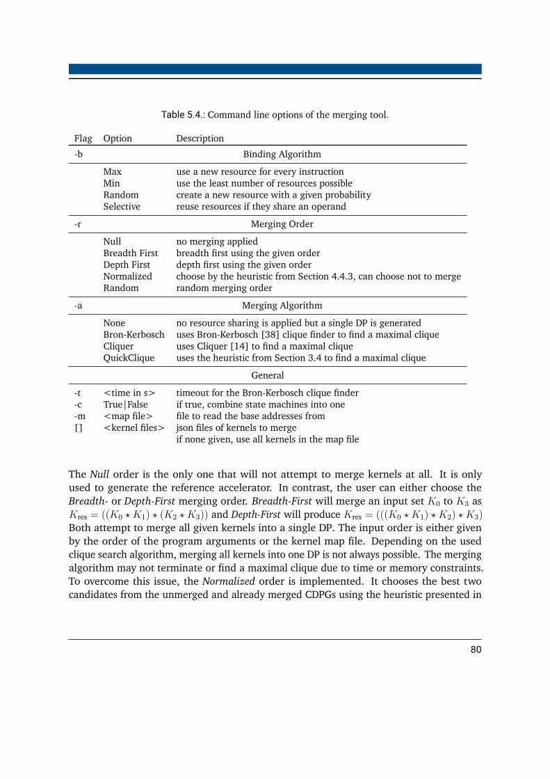
Table 5.4.: Command line options of the merging tool.
Flag Option Description-b Binding Algorithm
Max use a new resource for every instructionMin use the least number of resources possibleRandom create a new resource with a given probabilitySelective reuse resources if they share an operand
-r Merging Order
Null no merging appliedBreadth First breadth first using the given orderDepth First depth first using the given orderNormalized choose by the heuristic from Section 4.4.3, can choose not to mergeRandom random merging order
-a Merging Algorithm
None no resource sharing is applied but a single DP is generatedBron-Kerbosch uses Bron-Kerbosch [38] clique finder to find a maximal cliqueCliquer uses Cliquer [14] to find a maximal cliqueQuickClique uses the heuristic from Section 3.4 to find a maximal clique
General
-t <time in s> timeout for the Bron-Kerbosch clique finder-c True|False if true, combine state machines into one-m <map file> file to read the base addresses from[] <kernel files> json files of kernels to merge
if none given, use all kernels in the map file
The Null order is the only one that will not attempt to merge kernels at all. It is onlyused to generate the reference accelerator. In contrast, the user can either choose theBreadth- or Depth-First merging order. Breadth-First will merge an input set K0 to K3 asKres = ((K0 ⋆ K1) ⋆ (K2 ⋆ K3)) and Depth-First will produce Kres = (((K0 ⋆ K1) ⋆ K2) ⋆ K3)
Both attempt to merge all given kernels into a single DP. The input order is either givenby the order of the program arguments or the kernel map file. Depending on the usedclique search algorithm, merging all kernels into one DP is not always possible. The mergingalgorithm may not terminate or find a maximal clique due to time or memory constraints.To overcome this issue, the Normalized order is implemented. It chooses the best twocandidates from the unmerged and already merged CDPGs using the heuristic presented in
80

Memory Bus Peripheral Bus
Decoder
Wrapper
FSM
FSM
MergedDatapath
(a) A two-kernel accelerator sing a commonmergedDP.
Memory Bus Peripheral Bus
Decoder
Wrapper
MergedDatapath
JoinedFSM
(b) A two-kernel accelerator using a commonmerged DP and a joined FSM.
Figure 5.7.: Two levels of merging hardware accelerators.
Section 4.4.3. It also analyzes, if the problem size is suitable for the clique search algorithmand can decide to not merge. This limit results in an accelerator that has multiple wrappersof which every one has a merged DP. Figure 5.8 shows one possible scenario with four inputkernels. In a first step, kernel K1 and K2 are merged and in a second step K3 is added tothe result. Afterwards, it is checked if it is applicable to merge K0, which is not the case.Thus, two wrappers are generated. One containing the merged DPs of K1 to K3 and theother one containing only K0.
K0
K1
K2
K3
K0
K12
K3
K0
K312Wrapper312 Wrapper0
Accelerator
Merge Merge Generate
Figure 5.8.: Possible merging result using the Normalized order on four kernels. K0 is not mergedinto the others and generates its own wrapper.
81

+ -
Figure 5.9.: Combinatorial cycle due to reversely ordered and chained instructions which are boundto the same hardware unit.
5.4. Hardware Generation Challenges
As for the EP generation from Chapter 4 the merging process is based on DPGs. The resultingDPG must later be turned into an HDL code that implements the actual DP. Although thisstep is not the main concern of this work, some problems should not be left unmentioned.As before, they are related to cycles that are formed during the merging process. In the firstcase study it was required that the resulting merged DPG had no cycles because of its pipelinestructure. Therefore, this problem had to be solved during the merging process. Whenhardware accelerators are merged, the input DPGs already contain cycles which makes theprevious approach inapplicable. Furthermore, avoiding cycles is not even necessary as longas they are not purely combinatorial in the DP because the schedule is already generated bythe PIRANHA-plugin.
Figure 5.9 shows a possible cycle that is formed due to resource sharing within the kernelaccelerator. In one state an add operation is chained with a subsequent sub operation.In a different state a sub operation precedes an add operation. When both the additionsand subtractions are bound to the same corresponding computation unit they form theshown cycle. One can see that if there were registers placed in-between the operations, nocombinatorial cycle could be formed. This can only happen due to the chaining option thatpacks multiple subsequent operations into a single state. Depending on how the multiplexersare selected, either +- or -+ is executed. As it is a priori known that no other combinationis selected during runtime, the cycle is never electrically closed. That said, there is oneexception from the last statement.
82
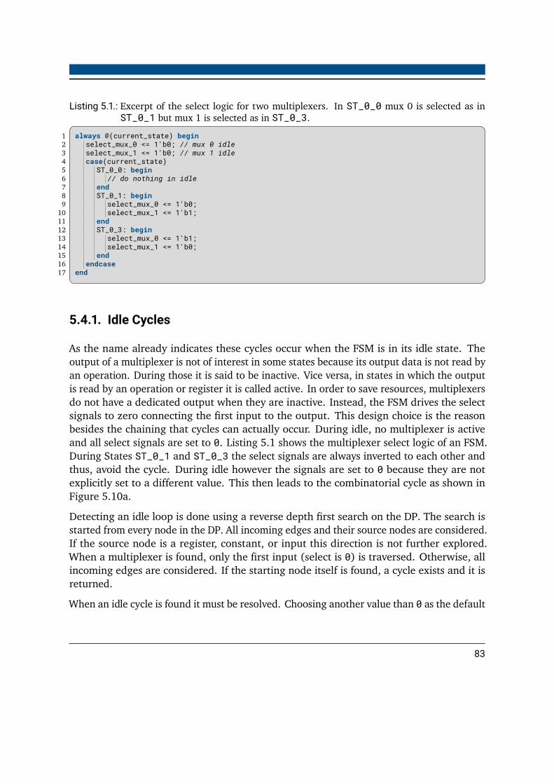
Listing 5.1.: Excerpt of the select logic for two multiplexers. In ST_0_0 mux 0 is selected as inST_0_1 but mux 1 is selected as in ST_0_3.
1 always @(current_state) begin2 select_mux_0 <= 1'b0; // mux 0 idle3 select_mux_1 <= 1'b0; // mux 1 idle4 case(current_state)5 ST_0_0: begin6 // do nothing in idle7 end8 ST_0_1: begin9 select_mux_0 <= 1'b0;
10 select_mux_1 <= 1'b1;11 end12 ST_0_3: begin13 select_mux_0 <= 1'b1;14 select_mux_1 <= 1'b0;15 end16 endcase17 end
5.4.1. Idle Cycles
As the name already indicates these cycles occur when the FSM is in its idle state. Theoutput of a multiplexer is not of interest in some states because its output data is not read byan operation. During those it is said to be inactive. Vice versa, in states in which the outputis read by an operation or register it is called active. In order to save resources, multiplexersdo not have a dedicated output when they are inactive. Instead, the FSM drives the selectsignals to zero connecting the first input to the output. This design choice is the reasonbesides the chaining that cycles can actually occur. During idle, no multiplexer is activeand all select signals are set to 0. Listing 5.1 shows the multiplexer select logic of an FSM.During States ST_0_1 and ST_0_3 the select signals are always inverted to each other andthus, avoid the cycle. During idle however the signals are set to 0 because they are notexplicitly set to a different value. This then leads to the combinatorial cycle as shown inFigure 5.10a.
Detecting an idle loop is done using a reverse depth first search on the DP. The search isstarted from every node in the DP. All incoming edges and their source nodes are considered.If the source node is a register, constant, or input this direction is not further explored.When a multiplexer is found, only the first input (select is 0) is traversed. Otherwise, allincoming edges are considered. If the starting node itself is found, a cycle exists and it isreturned.
When an idle cycle is found it must be resolved. Choosing another value than 0 as the default
83
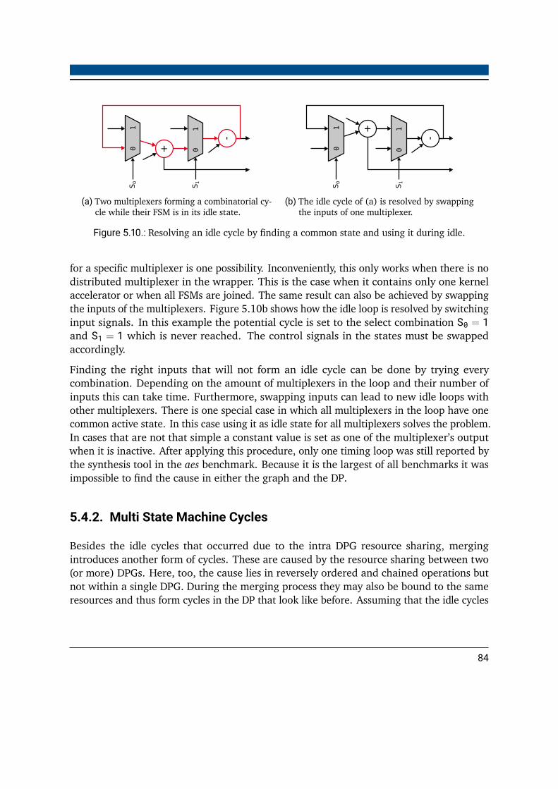
01
+ 01
S0
S1
-
(a) Two multiplexers forming a combinatorial cy-cle while their FSM is in its idle state.
01 +
01
S0
S1
-
(b) The idle cycle of (a) is resolved by swappingthe inputs of one multiplexer.
Figure 5.10.: Resolving an idle cycle by finding a common state and using it during idle.
for a specific multiplexer is one possibility. Inconveniently, this only works when there is nodistributed multiplexer in the wrapper. This is the case when it contains only one kernelaccelerator or when all FSMs are joined. The same result can also be achieved by swappingthe inputs of the multiplexers. Figure 5.10b shows how the idle loop is resolved by switchinginput signals. In this example the potential cycle is set to the select combination S0 = 1and S1 = 1 which is never reached. The control signals in the states must be swappedaccordingly.
Finding the right inputs that will not form an idle cycle can be done by trying everycombination. Depending on the amount of multiplexers in the loop and their number ofinputs this can take time. Furthermore, swapping inputs can lead to new idle loops withother multiplexers. There is one special case in which all multiplexers in the loop have onecommon active state. In this case using it as idle state for all multiplexers solves the problem.In cases that are not that simple a constant value is set as one of the multiplexer’s outputwhen it is inactive. After applying this procedure, only one timing loop was still reported bythe synthesis tool in the aes benchmark. Because it is the largest of all benchmarks it wasimpossible to find the cause in either the graph and the DP.
5.4.2. Multi State Machine Cycles
Besides the idle cycles that occurred due to the intra DPG resource sharing, mergingintroduces another form of cycles. These are caused by the resource sharing between two(or more) DPGs. Here, too, the cause lies in reversely ordered and chained operations butnot within a single DPG. During the merging process they may also be bound to the sameresources and thus form cycles in the DP that look like before. Assuming that the idle cycles
84

Listing 5.2.: Excerpt of the Verilog code controlling the multiplexers in a DP.
1 // FSM 02 always @(c_state) begin3 case(c_state)4 ST_0_3: begin5 fsm0_s0 <= 1'b0;6 fsm0_s1 <= 1'b1;7 end8 endcase9 end
1 // FSM 12 always @(c_state) begin3 case(c_state)4 ST_1_8: begin5 fsm1_s0 <= 1'b1;6 fsm1_s1 <= 1'b0;7 end8 endcase9 end
1 // Wrapper Module with Distributed Multiplexer2 assign datapath_s0 = fsm0_s0 | fsm1_s0;3 assign datapath_s1 = fsm0_s1 | fsm1_s1;
have already been resolved they cannot be closed during runtime. Listing 5.2 together withFigure 5.10 shows why. Both FSMs set the multiplexer select signals such that the cycle isnever closed during runtime.
Nevertheless, the timing analysis tool does not know that the FSMs will not be active simul-taneously. Theoretically FSM0 can be in ST_0_3 and FSM1 can be in ST_1_8 concurrently.Together with the distributed multiplexer in the wrapper this would lead to the S0 = 1 andS1 = 1 combination closing the cycle. Therefore, the synthesis tool will raise a warning dur-ing the timing analysis. This must then be resolved by either excluding the cyclic path fromthe timing analysis or state machine joining which is explained in detail in Section 5.6.4.
85
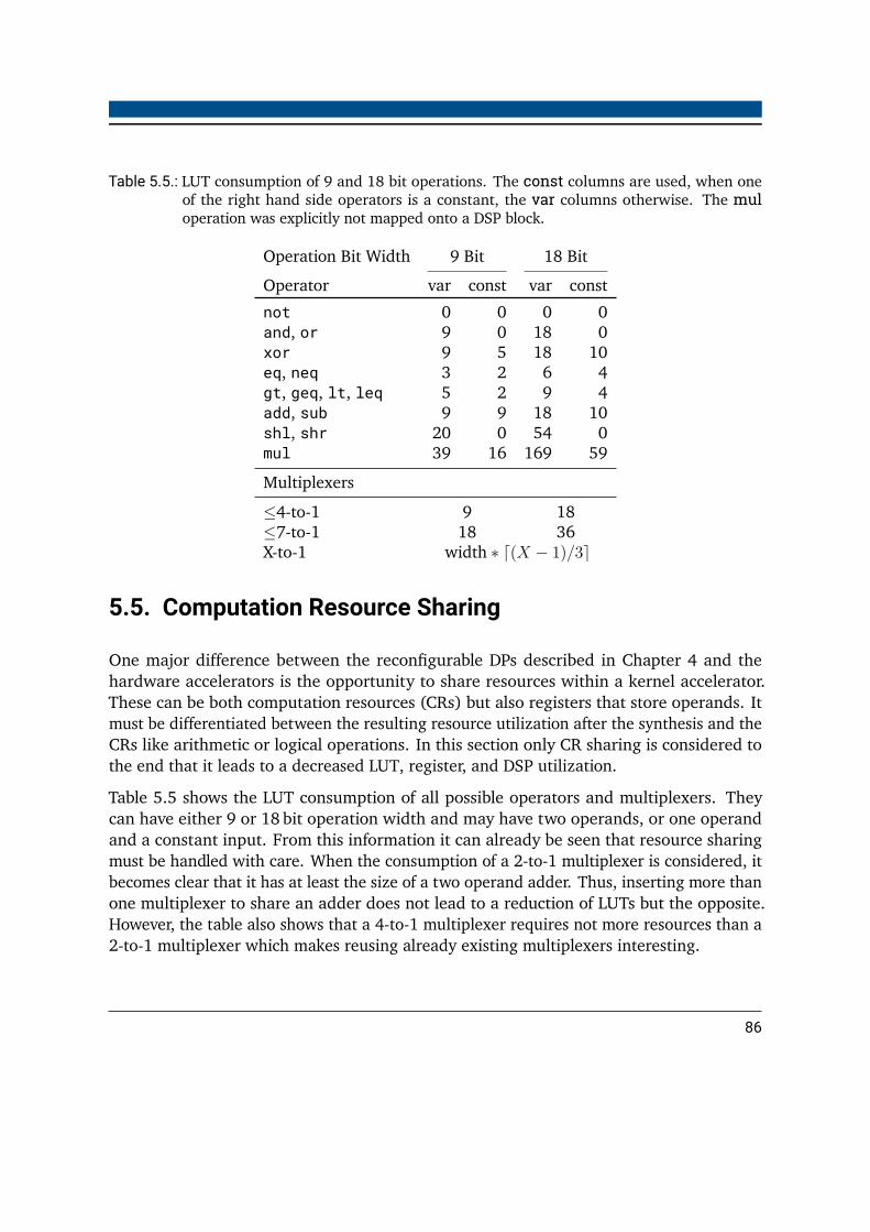
Table 5.5.: LUT consumption of 9 and 18 bit operations. The const columns are used, when oneof the right hand side operators is a constant, the var columns otherwise. The muloperation was explicitly not mapped onto a DSP block.
Operation Bit Width 9 Bit 18 Bit
Operator var const var constnot 0 0 0 0and, or 9 0 18 0xor 9 5 18 10eq, neq 3 2 6 4gt, geq, lt, leq 5 2 9 4add, sub 9 9 18 10shl, shr 20 0 54 0mul 39 16 169 59
Multiplexers
≤4-to-1 9 18≤7-to-1 18 36X-to-1 width ∗ ⌈(X − 1)/3⌉
5.5. Computation Resource Sharing
One major difference between the reconfigurable DPs described in Chapter 4 and thehardware accelerators is the opportunity to share resources within a kernel accelerator.These can be both computation resources (CRs) but also registers that store operands. Itmust be differentiated between the resulting resource utilization after the synthesis and theCRs like arithmetic or logical operations. In this section only CR sharing is considered tothe end that it leads to a decreased LUT, register, and DSP utilization.
Table 5.5 shows the LUT consumption of all possible operators and multiplexers. Theycan have either 9 or 18 bit operation width and may have two operands, or one operandand a constant input. From this information it can already be seen that resource sharingmust be handled with care. When the consumption of a 2-to-1 multiplexer is considered, itbecomes clear that it has at least the size of a two operand adder. Thus, inserting more thanone multiplexer to share an adder does not lead to a reduction of LUTs but the opposite.However, the table also shows that a 4-to-1 multiplexer requires not more resources than a2-to-1 multiplexer which makes reusing already existing multiplexers interesting.
86
Due to logic optimizations the multiplexer logic can sometimes be (partially) fused intopreceding or subsequent logic. Whenever LUTs are estimated in this section, this effect isneglected because the logic optimizer is hard to predict. Therefore, the LUT requirementsof each component are simply summed up.
5.5.1. Binding Algorithms
In the publications [48, 49] Fazlali et al. bind hardware resources before merging the DPs.Their starting point is a set of already scheduled and bound DPGs. If not stated explicitlyotherwise, this order is maintained throughout this chapter. Although this work’s main goalis not to find a new binding algorithm for hardware accelerators, at least a functional andwell performing binding must be implemented.
Resource limits can be given at kernel level. The table contains an amount of computationresources for the combination of each:
• Operator (add, sub, eq, ...)
• Bit Width (9 or 18)
• Signedness (only one (false) if not applicable)
In total, 33 combinations exist and are called a CR’s type. A complete resource table can befound in Table A.5.Globally limiting the resources is not an option as it automatically implies a priority depend-ing on the order in which kernels are bound. One exception is made for the memory port,which is treated as a resource as well. In all test scenarios there is only one memory portthat is shared by all kernel accelerators. As a result of that, all memory instructions arebound on the same resource and thus no prioritizing occurs.
Scoring Shared Resources Whenever a CR must be found for an instruction there aremultiple options. Of course, if no CR of the required type exists a new one must be created.However, if multiple CRs already exist one has to be selected.
In order to find the most suitable one they are scored by a simple strategy. In the beginning,every CR has a score of zero. Now, for every operation that is already bound to the CRit is checked if it has the same output operand as the instruction to be bound. If twooperations of the same type with the same output operand were mapped to different CRs, a
87
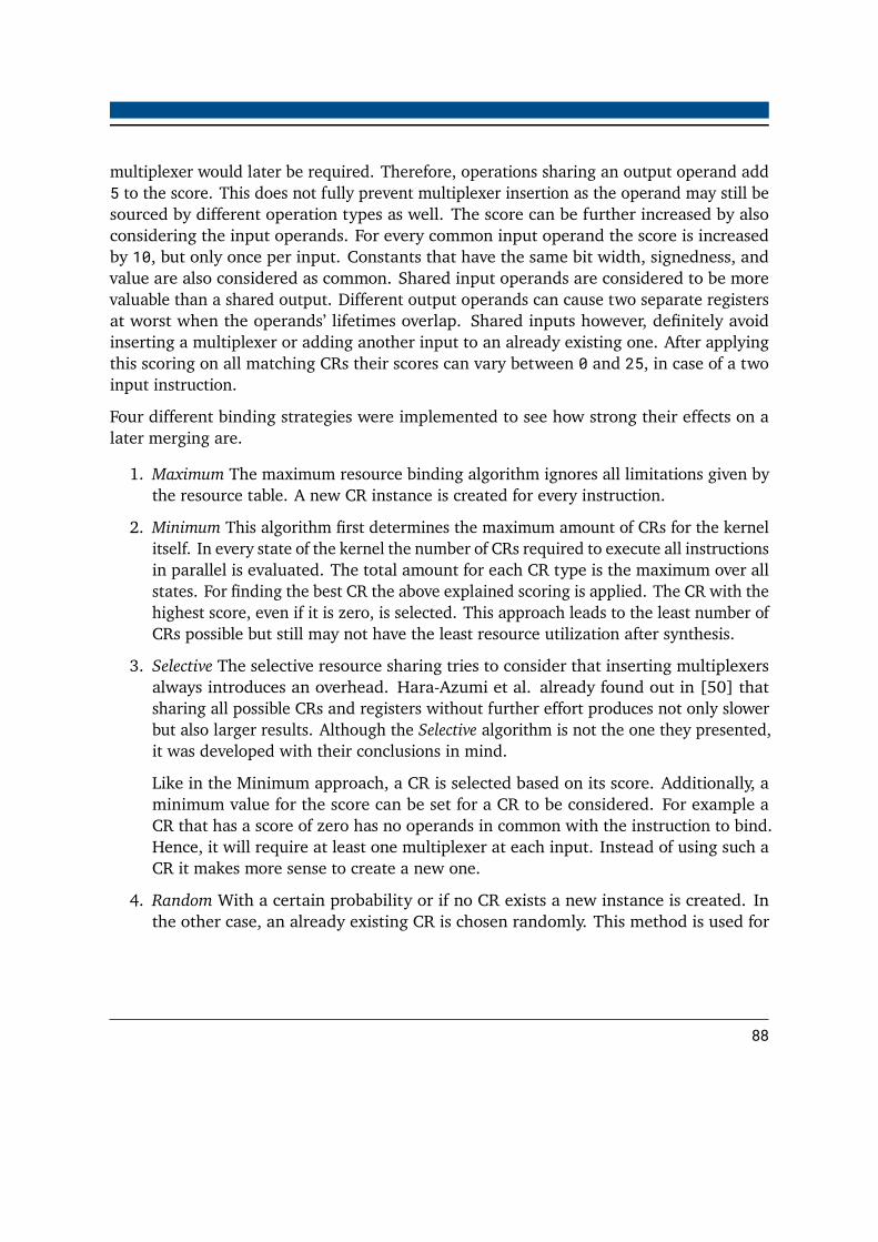
multiplexer would later be required. Therefore, operations sharing an output operand add5 to the score. This does not fully prevent multiplexer insertion as the operand may still besourced by different operation types as well. The score can be further increased by alsoconsidering the input operands. For every common input operand the score is increasedby 10, but only once per input. Constants that have the same bit width, signedness, andvalue are also considered as common. Shared input operands are considered to be morevaluable than a shared output. Different output operands can cause two separate registersat worst when the operands’ lifetimes overlap. Shared inputs however, definitely avoidinserting a multiplexer or adding another input to an already existing one. After applyingthis scoring on all matching CRs their scores can vary between 0 and 25, in case of a twoinput instruction.
Four different binding strategies were implemented to see how strong their effects on alater merging are.
1. Maximum The maximum resource binding algorithm ignores all limitations given bythe resource table. A new CR instance is created for every instruction.
2. Minimum This algorithm first determines the maximum amount of CRs for the kernelitself. In every state of the kernel the number of CRs required to execute all instructionsin parallel is evaluated. The total amount for each CR type is the maximum over allstates. For finding the best CR the above explained scoring is applied. The CR with thehighest score, even if it is zero, is selected. This approach leads to the least number ofCRs possible but still may not have the least resource utilization after synthesis.
3. Selective The selective resource sharing tries to consider that inserting multiplexersalways introduces an overhead. Hara-Azumi et al. already found out in [50] thatsharing all possible CRs and registers without further effort produces not only slowerbut also larger results. Although the Selective algorithm is not the one they presented,it was developed with their conclusions in mind.
Like in the Minimum approach, a CR is selected based on its score. Additionally, aminimum value for the score can be set for a CR to be considered. For example aCR that has a score of zero has no operands in common with the instruction to bind.Hence, it will require at least one multiplexer at each input. Instead of using such aCR it makes more sense to create a new one.
4. Random With a certain probability or if no CR exists a new instance is created. Inthe other case, an already existing CR is chosen randomly. This method is used for
88
>=
0 1
+
25
A B
(a) Original DP without sharedregisters.
>=
0 1
+
25
A,B
(b) Step 1: Share the register.
>=
+
25
A,B
(c) Step 2: Remove the multi-plexer.
Figure 5.11.: Best case for sharing registers. The operands’ lifetimes are disjoint and their sourceoperations’ CR is the same.
evaluating the possible spread in resulting resource utilization depending on thebinding.
5.5.2. Register Fusing
All the above mentioned binding techniques (except Maximum) will lead to a certain degreeof shared CR. During the resource binding no assumptions are made about the lifetimesof the operands. It would be possible to share registers with for example the left edgealgorithm. However, for shared registers the same applies as for shared CRs. Without anyknowledge about the operations that source the registers this can lead to an unnecessarilyhigh amount of multiplexers.
Nevertheless, register sharing should not be completely omitted. Leaving this task to thesynthesis tools will not produce the results one may like to have. In fact, they can detectwhen two registers are equal and then purge one of them. Nevertheless, this only works ifboth their input signals and the control signal are equal. While the former one is probablyoften the case after resource binding, the latter is impossible to happen concurrently. Notonly the lifetimes of the operands would have to match but also the states in which they arewritten. This requirement automatically disqualifies their sourcing instructions to be boundto the same CR instance. Thus, they can share either the same input or the same controlsignal, but not both.
89
Therefore, register sharing can only be applied before synthesis when there is still knowledgeabout the operands lifetimes. Generally, registers can be shared if their stored operandlifetimes are disjoint. With the restriction that they are only shared when their sourcingoperation(s) are equal, a reduction in registers can be achieved without additional mul-tiplexing. Furthermore, operands that share a register can even reduce the number ofrequired subsequent multiplexers. Figure 5.11 shows this best case scenario. An operationhas operand A and operand B as its input at port 0. If A and B are now placed into the sameregister, the multiplexer at that input port can be omitted or at least be reduced by oneinput.
5.5.3. Results
The effect on the different binding techniques can be seen in Table 5.6. It shows the resourceconsumption of the fletcher benchmark after binding and implementation using the firstthree binding strategies. The fletcher benchmark is only used exemplarily. The effectsdescribed in the following apply for nearly all other benchmarks as well.
As expected, theMaximum strategy has the highest number of CRs. All inserted multiplexersare solely required to select the correct input for a register to store an operand. It canclearly be seen that there is a trade-off between CRs and multiplexers when the Maximumis compared to the Minimum strategy. Especially, the 2-to-1 multiplexers increase strongly.
Using Table 5.5 one can give an upper and a lower estimate for the resource saving due toshared CRs. The lower estimate assumes that all operations have a constant as one of itsright hand side operands. The number of LUTs required for a CR multiplied by the numberof saved instances compared to the Maximum binding then gives the estimate. For example,the number of saved 9 bit equals is 9 and they require 2 LUTs each, which contribute 18saved LUTs. The lower bound is in total a saving of 282 LUTs. To calculate the upper boundof savings, it is assumed that all operations only have non-constant operands. The equalsthen require 3 LUTs resulting in 27 saved LUTs. This leads to an estimated LUT saving of468 LUTs in total. The estimated increase due to the multiplexers is 153 LUTs. In contrast tothe first assumption about the Minimum binding, in both the best and worst case an overallsaving in resources would be expected. However, the synthesis results do not reflect theseestimations. In fact, the Minimum binding uses 147 more LUTs than the Maximum bindingafter the implementation which again confirms the first assumption.
The Selective strategy however seems to perform better. The number of CRs decreases closeto the level of the Minimum strategy. Furthermore, it does not insert more multiplexers than
90
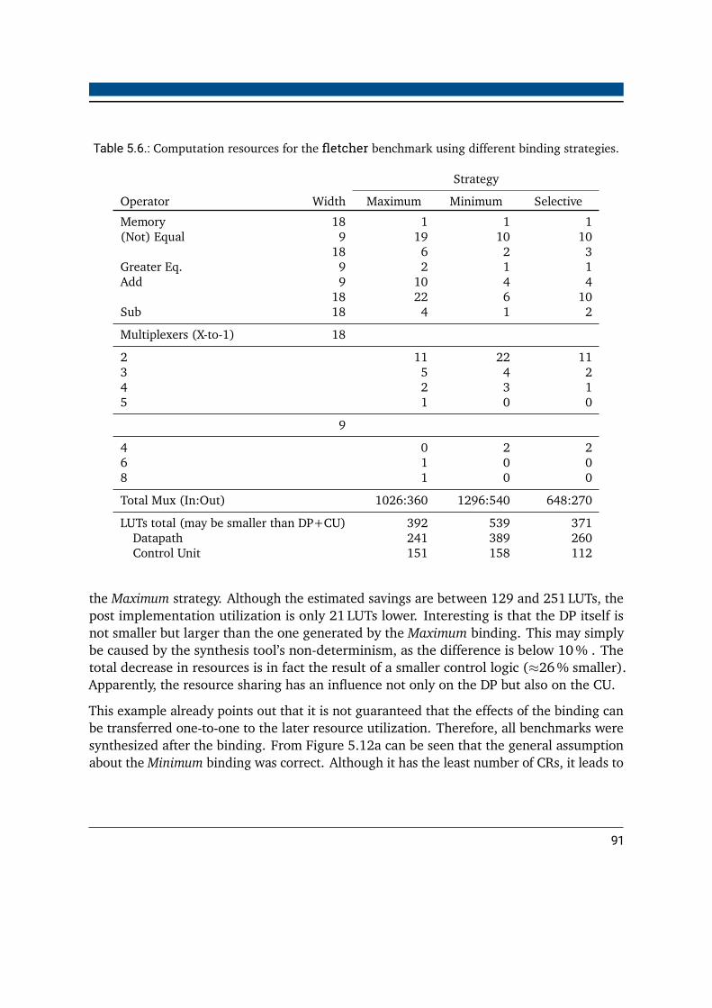
Table 5.6.: Computation resources for the fletcher benchmark using different binding strategies.
Strategy
Operator Width Maximum Minimum SelectiveMemory 18 1 1 1(Not) Equal 9 19 10 10
18 6 2 3Greater Eq. 9 2 1 1Add 9 10 4 4
18 22 6 10Sub 18 4 1 2
Multiplexers (X-to-1) 18
2 11 22 113 5 4 24 2 3 15 1 0 0
9
4 0 2 26 1 0 08 1 0 0
Total Mux (In:Out) 1026:360 1296:540 648:270
LUTs total (may be smaller than DP+CU) 392 539 371Datapath 241 389 260Control Unit 151 158 112
the Maximum strategy. Although the estimated savings are between 129 and 251 LUTs, thepost implementation utilization is only 21 LUTs lower. Interesting is that the DP itself isnot smaller but larger than the one generated by the Maximum binding. This may simplybe caused by the synthesis tool’s non-determinism, as the difference is below 10% . Thetotal decrease in resources is in fact the result of a smaller control logic (≈26% smaller).Apparently, the resource sharing has an influence not only on the DP but also on the CU.
This example already points out that it is not guaranteed that the effects of the binding canbe transferred one-to-one to the later resource utilization. Therefore, all benchmarks weresynthesized after the binding. From Figure 5.12a can be seen that the general assumptionabout the Minimum binding was correct. Although it has the least number of CRs, it leads to
91
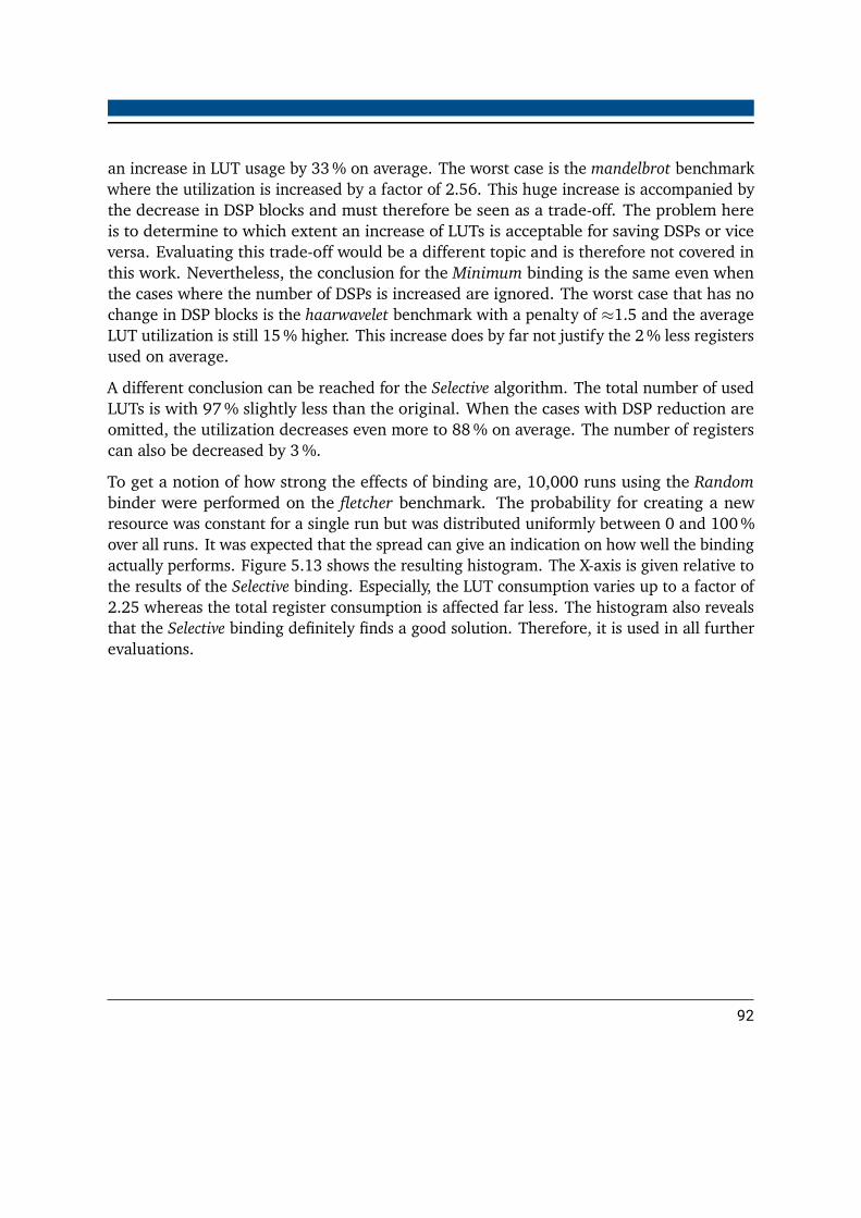
an increase in LUT usage by 33% on average. The worst case is the mandelbrot benchmarkwhere the utilization is increased by a factor of 2.56. This huge increase is accompanied bythe decrease in DSP blocks and must therefore be seen as a trade-off. The problem hereis to determine to which extent an increase of LUTs is acceptable for saving DSPs or viceversa. Evaluating this trade-off would be a different topic and is therefore not covered inthis work. Nevertheless, the conclusion for the Minimum binding is the same even whenthe cases where the number of DSPs is increased are ignored. The worst case that has nochange in DSP blocks is the haarwavelet benchmark with a penalty of ≈1.5 and the averageLUT utilization is still 15% higher. This increase does by far not justify the 2% less registersused on average.
A different conclusion can be reached for the Selective algorithm. The total number of usedLUTs is with 97% slightly less than the original. When the cases with DSP reduction areomitted, the utilization decreases even more to 88% on average. The number of registerscan also be decreased by 3%.
To get a notion of how strong the effects of binding are, 10,000 runs using the Randombinder were performed on the fletcher benchmark. The probability for creating a newresource was constant for a single run but was distributed uniformly between 0 and 100%over all runs. It was expected that the spread can give an indication on how well the bindingactually performs. Figure 5.13 shows the resulting histogram. The X-axis is given relative tothe results of the Selective binding. Especially, the LUT consumption varies up to a factor of2.25 whereas the total register consumption is affected far less. The histogram also revealsthat the Selective binding definitely finds a good solution. Therefore, it is used in all furtherevaluations.
92
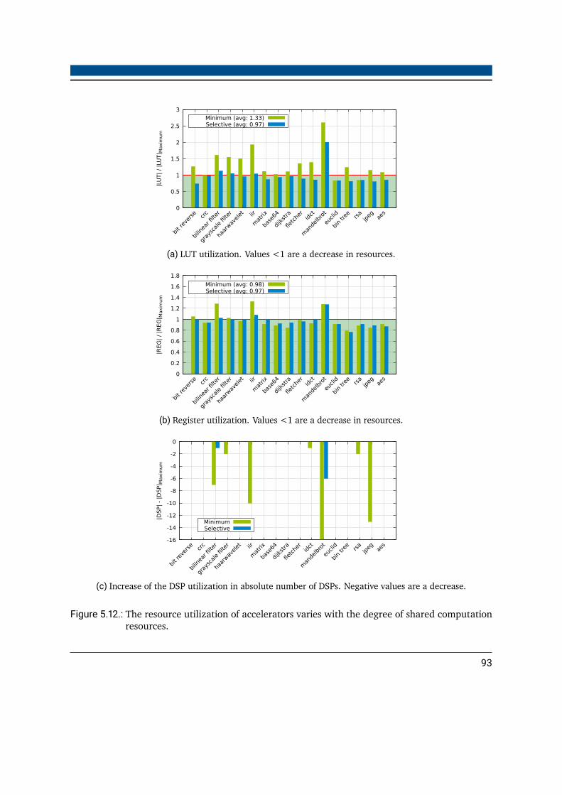
0
0.5
1
1.5
2
2.5
3
bit r
ever
se crc
bilin
ear fi
lter
gray
scale fil
ter
haar
wavelet iir
mat
rix
base
64
dijkst
ra
fletc
her
idct
man
delb
rot
euclid
bin
tree
rsa
jpeg ae
s
|LU
T|
/ |L
UT| M
axim
um
Minimum (avg: 1.33)Selective (avg: 0.97)
(a) LUT utilization. Values <1 are a decrease in resources.
0
0.2
0.4
0.6
0.8
1
1.2
1.4
1.6
1.8
bit r
ever
se crc
bilin
ear fi
lter
gray
scale fil
ter
haar
wavelet iir
mat
rix
base
64
dijkst
ra
fletc
her
idct
man
delb
rot
euclid
bin
tree
rsa
jpeg ae
s
|REG
| /
|REG
| Maxim
um
Minimum (avg: 0.98)Selective (avg: 0.97)
(b) Register utilization. Values <1 are a decrease in resources.
-16
-14
-12
-10
-8
-6
-4
-2
0
bit r
ever
se crc
bilin
ear fi
lter
gray
scale fil
ter
haar
wavelet iir
mat
rix
base
64
dijkst
ra
fletc
her
idct
man
delb
rot
euclid
bin
tree
rsa
jpeg ae
s
|DS
P|
- |D
SP| M
axim
um
MinimumSelective
(c) Increase of the DSP utilization in absolute number of DSPs. Negative values are a decrease.
Figure 5.12.: The resource utilization of accelerators varies with the degree of shared computationresources.
93
0
5
10
15
20
25
30
35
0.8 1 1.2 1.4 1.6 1.8 2 2.2 2.4 0
0.5
1
1.5
2
2.5
3
3.5
4
4.5
5
Selective
% o
f S
ynth
esi
s R
egis
ters
% o
f S
ynth
esi
s LU
Ts
Normalized LUTs and Registers
LUTsRegisters
Figure 5.13.: Resource utilization distribution for 10,000 Random binding runs of the fletcherbenchmark. All values are normalized to the Selective Binding.
94
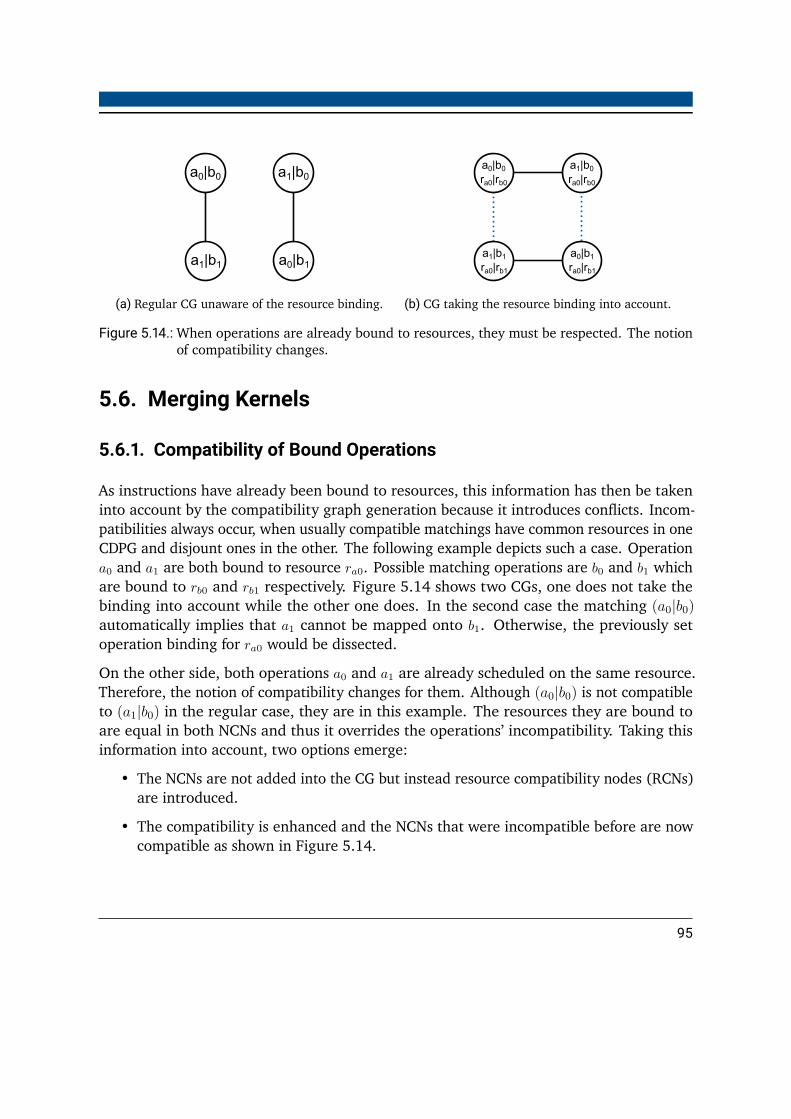
a0|b0 a1|b0
a0|b1a1|b1
(a) Regular CG unaware of the resource binding.
a0|b0ra0|rb0
a1|b0ra0|rb0
a0|b1ra0|rb1
a1|b1ra0|rb1
(b) CG taking the resource binding into account.
Figure 5.14.: When operations are already bound to resources, they must be respected. The notionof compatibility changes.
5.6. Merging Kernels
5.6.1. Compatibility of Bound Operations
As instructions have already been bound to resources, this information has then be takeninto account by the compatibility graph generation because it introduces conflicts. Incom-patibilities always occur, when usually compatible matchings have common resources in oneCDPG and disjount ones in the other. The following example depicts such a case. Operationa0 and a1 are both bound to resource ra0. Possible matching operations are b0 and b1 whichare bound to rb0 and rb1 respectively. Figure 5.14 shows two CGs, one does not take thebinding into account while the other one does. In the second case the matching (a0|b0)automatically implies that a1 cannot be mapped onto b1. Otherwise, the previously setoperation binding for ra0 would be dissected.
On the other side, both operations a0 and a1 are already scheduled on the same resource.Therefore, the notion of compatibility changes for them. Although (a0|b0) is not compatibleto (a1|b0) in the regular case, they are in this example. The resources they are bound toare equal in both NCNs and thus it overrides the operations’ incompatibility. Taking thisinformation into account, two options emerge:
• The NCNs are not added into the CG but instead resource compatibility nodes (RCNs)are introduced.
• The compatibility is enhanced and the NCNs that were incompatible before are nowcompatible as shown in Figure 5.14.
95

+
&
a0 a1
a2
8
(a) CDPGA
+
&
b0
b1
+
*
b2
b3
(b) CDPGB
a0|b0 a0|b2
a2|b1a0a2b0b1
(c) CG of CDPGA and CDPGB
Figure 5.15.: Selective compatibility: Although (a0|b2) is compatible to (a2|b1) they are not connectedby an edge in the CG.
It was decided to implement the second option using multiple NCNs and let them have ahigher influence during clique search.
5.6.2. Selective Matchability
The merging process itself is based on the CG approach that was introduced in Chapter 3.Nevertheless, the CG creation has some peculiarities depending on the input problems. Inmerging CDPGs for generating reconfigurable EPs it was the operation order that had to betaken into account. Here, it is the operation’s resource consumption. As it can be takenfrom Table 5.5 not all resources are worth sharing. Even further, some operations do notgenerate hardware at all when one of their input operands is a constant. For example, ashift by a constant only affects the wiring of the resulting hardware but does not add anyLUTs. Hence, adding the LUTs for a multiplexer to share it is counterproductive. Therefore,such operations will not produce a CN on their own. Only if their preceding operations arematchable, a CN is added to the CG. In the best case, when the subsequent operation isshared as well, it may also reduce the input multiplexer size.
This approach can be seen in the example in Figure 5.15. It is clearly more useful to map a0onto b0 instead of b2 because the following and operation can be shared as well. If (a2|b1) isnot added to the CG, both mappings are equally valuable and one will be chosen arbitrarily.Adding (a2|b1) automatically leads to the ECN (a0a2|b0b1) and the formed triangle of CNswill be preferred over (a0|b2).
Choosing (a2|b1)without (a0|b0) is not reasonable because it leads to an unnecessary insertionof multiplexers. Unfortunately, there is no guarantee that they will always be chosen in
96

combination. If a node that is incompatible to (a0|b0) is selected, (a2|b1)may still be selectedas well. Such a node is represented by (a0|b2). In order to avoid cliques that contain (a2|b1)but not (a0|b0) not all possible edges of (a2|b1) are added. The dotted edge in Figure 5.15shows such a case.
For low- or zero cost operations edges are only inserted when the other touching CN iscompatible to a predecessor matching. If no predecessor matching exists, they are completelyunconnected and can thus be removed from the CG. In the implementation, all regularmatchings are inspected for low cost successor matchings, which are then added accordingly.The maximality requirement of the clique finders then ensures that whenever (a2|b1) isselected, the other two are selected as well.
5.6.3. Basic Merging Performance
In Chapter 4 the QuickClique heuristic has shown to produce good results in finding largecliques in dense CGs. To ensure that this assumption is still valid, the user can choose theclique finding algorithm depending his needs. As before, the three possibilities are:
1. Bron-Kerbosch In principle, this algorithm can deliver the exact maximum clique.Taking the problem sizes into account it will most likely never finish. Therefore, atime limit can be set. When this is reached, the largest clique that was found so far isreturned. It can happen, that even after the time limit is reached no clique is found.This occurs due to the fact, that the algorithms only enumerates and returns maximalcliques. If the CG is very large the limit might not be enough to find even one.
2. Cliquer Is the heuristic that can handle weighted and unweighted CGs. Because Cliqueris a native command line tool, the CG must be exported into the DIMACS [18] format.Afterwards, the result has to be parsed accordingly. Unfortunately, no time limit canbe set. After a certain amount of time the process is simply terminated but withoutany result.
3. QuickClique The clique searching heuristic that was presented in Section 3.4.
It was not clear, if the choice of the clique search algorithm has a strong effect on theresulting hardware size. Thus, the first tests were conducted without joining the FSMs tonot have two effects interfere with each other. For these tests, a neutral baseline has tobe chosen. This was generated by using the Null merging order and Selective CR sharing.The baseline results can be found in Table 5.7. Benchmarks that only have one kernel areomitted from this point on as merging has no effect on them. The LUT utilization have
97

Table 5.7.: Baseline for the resource utilization evaluation of merged accelerators. For CR sharingthe Selective strategy is used and registers are fused afterwards. Every kernel has itsown DP and CU.
Benchmark Kernels LUTs Registers DSPsbase64 2 560.0 925 0dijkstra 2 479.0 925 1fletcher 2 376.0 623 0idct 2 579.0 1205 2mandelbrot 2 1158.0 1394 19euclid 3 266.0 369 0bin tree 6 551.0 817 0rsa 12 1398.5 2360 4jpeg 15 4860.5 8189 26aes 19 3300.0 5432 0
one decimal place that can be either .0 or .5 . This notation reflects the fact that the usedFPGA has LUTs that can be split. It can be either one six-input LUT with one output or twofive-input LUTs with two outputs. Accordingly, whenever a 5-input LUT is used, it is onlycounted as half.
Figure 5.16 show the results of the merging which are normalized to the baseline. Exceptone outlier, it can be confirmed that only joining kernels into one DP using the Nonemergingproduces similar results as the reference hardware. The other slight differences can beexplained by the synthesis tools being non-deterministic 1. The time limit for the Bron-Kerbosch clique finder was set to 30 minutes for every merging step. It was first tried to usethe Breadth-First order for merging to obtain a single DP for every benchmark. In caseswere the clique finding algorithms did not terminate due to memory or time limits, theNormalized order was used again. These cases are rsa, jpeg, and aes. The QuickCliquealgorithm could then terminate in all cases. Bron-Kerbosch was yet not able to finish the jpegbenchmark because it ran out of memory. The CG where it failed had 118 nodes and 6,375edges. This is inconvenient, especially because it was able to find a clique in the previousstep in a graph with 2,160 nodes and 790,044 edges. Cliquer failed finding a clique whilemerging the aes and the jpeg benchmark. The jpeg benchmark failed at a CG with 2,197
1When exactly the same files are synthesized multiple times, the output will be equal. If only the logicfunctionality is equal, outputs may vary.
98

0
0.5
1
1.5
2
base
64
dijkst
ra
fletc
her
idct
man
delb
rot
eucli
d
bin
tree
rsa
(2)
jpeg
(4)
aes (3
)
|LU
T| S
ing
leD
P /
|LU
T| M
ult
iple
DP
none (avg. 1.02)bron-kerbosch (avg. 1.23)
cliquer (avg. 1.20)quick (avg. 1.22)
(a) Normalized LUT utilization. Values <1 are adecrease in resources.
0
0.5
1
1.5
2
base
64
dijkst
ra
fletc
her
idct
man
delb
rot
eucli
d
bin
tree
rsa
(2)
jpeg
(4)
aes (3
)
|REG
| Sin
gle
DP /
|R
EG
| Mult
iple
DP
none (avg. 1.09)bron-kerbosch (avg. 0.90)
cliquer (avg. 0.91)quick (avg. 0.88)
(b) Normalized register utilization. Values <1are a decrease in resources.
-10
-8
-6
-4
-2
0
2
base
64
dijkst
ra
fletc
her
idct
man
delb
rot
eucli
d
bin
tree
rsa
(2)
jpeg
(4)
aes (3
)
|DSP| S
ing
leD
P -
|D
SP| M
ult
iple
DP
nonebron-kerbosch
cliquerquick
(c) Increase of the DSP utilization. Negative val-ues are a decrease.
Figure 5.16.: Normalized hardware resource utilization depending on the clique finding algorithm.All clique based mergers increase the LUT utilization but slightly decrease the registerutilization. Numbers in brackets indicate the number of resulting DPs.
nodes and 2,348,094 edges and aes at 4,386 nodes and 3,874,047 edges. One must knowthat the CG size that is compared to the threshold is only based on the basic NCNs. Thus,the resulting CG is larger in all cases. This approximation was necessary because for largeCDPGs creating the complete CG already required to much memory.
The failing cases could only be enabled by lowering the CG size limit of the Normalized order.This would automatically increase the probability of more DPs in the resulting accelerator.Yet, it was decided to not further reduce the threshold as all clique finding algorithmsproduce similar overall results.
What Figure 5.16 also shows is that the results for the merged DPs do not reflect theresource savings that were expected. On the contrary, the LUT utilization increases by over20% on average whenever merging is performed. This effect can be seen as the merging
99
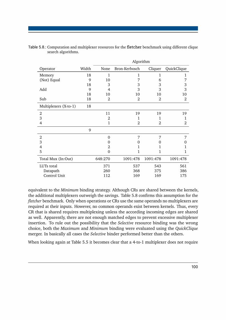
Table 5.8.: Computation and multiplexer resources for the fletcher benchmark using different cliquesearch algorithms.
Algorithm
Operator Width None Bron-Kerbosch Cliquer QuickCliqueMemory 18 1 1 1 1(Not) Equal 9 10 7 6 7
18 3 3 3 3Add 9 4 3 3 3
18 10 10 10 10Sub 18 2 2 2 2
Multiplexers (X-to-1) 18
2 11 19 19 193 2 1 1 14 1 2 2 2
9
2 0 7 7 73 0 0 0 04 2 1 1 15 0 1 1 1
Total Mux (In:Out) 648:270 1091:478 1091:478 1091:478
LUTs total 371 537 543 561Datapath 260 368 375 386Control Unit 112 169 169 175
equivalent to the Minimum binding strategy. Although CRs are shared between the kernels,the additional multiplexers outweigh the savings. Table 5.8 confirms this assumption for thefletcher benchmark. Only when operations or CRs use the same operands no multiplexers arerequired at their inputs. However, no common operands exist between kernels. Thus, everyCR that is shared requires multiplexing unless the according incoming edges are sharedas well. Apparently, there are not enough matched edges to prevent excessive multiplexerinsertion. To rule out the possibility that the Selective resource binding was the wrongchoice, both the Maximum and Minimum binding were evaluated using the QuickCliquemerger. In basically all cases the Selective binder performed better than the others.
When looking again at Table 5.5 it becomes clear that a 4-to-1 multiplexer does not require
100
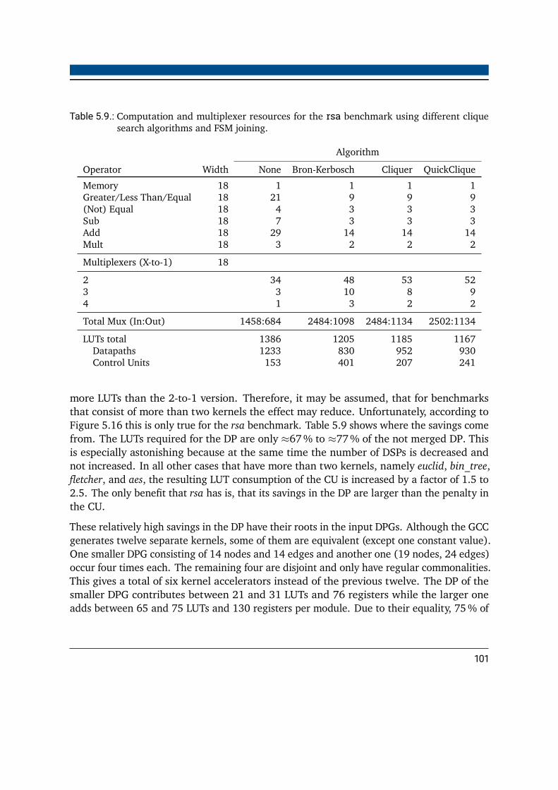
Table 5.9.: Computation and multiplexer resources for the rsa benchmark using different cliquesearch algorithms and FSM joining.
Algorithm
Operator Width None Bron-Kerbosch Cliquer QuickCliqueMemory 18 1 1 1 1Greater/Less Than/Equal 18 21 9 9 9(Not) Equal 18 4 3 3 3Sub 18 7 3 3 3Add 18 29 14 14 14Mult 18 3 2 2 2
Multiplexers (X-to-1) 18
2 34 48 53 523 3 10 8 94 1 3 2 2
Total Mux (In:Out) 1458:684 2484:1098 2484:1134 2502:1134
LUTs total 1386 1205 1185 1167Datapaths 1233 830 952 930Control Units 153 401 207 241
more LUTs than the 2-to-1 version. Therefore, it may be assumed, that for benchmarksthat consist of more than two kernels the effect may reduce. Unfortunately, according toFigure 5.16 this is only true for the rsa benchmark. Table 5.9 shows where the savings comefrom. The LUTs required for the DP are only ≈67% to ≈77% of the not merged DP. Thisis especially astonishing because at the same time the number of DSPs is decreased andnot increased. In all other cases that have more than two kernels, namely euclid, bin_tree,fletcher, and aes, the resulting LUT consumption of the CU is increased by a factor of 1.5 to2.5. The only benefit that rsa has is, that its savings in the DP are larger than the penalty inthe CU.
These relatively high savings in the DP have their roots in the input DPGs. Although the GCCgenerates twelve separate kernels, some of them are equivalent (except one constant value).One smaller DPG consisting of 14 nodes and 14 edges and another one (19 nodes, 24 edges)occur four times each. The remaining four are disjoint and only have regular commonalities.This gives a total of six kernel accelerators instead of the previous twelve. The DP of thesmaller DPG contributes between 21 and 31 LUTs and 76 registers while the larger oneadds between 65 and 75 LUTs and 130 registers per module. Due to their equality, 75% of
101

both LUTs and registers can be saved leading to a reduction of approximately 288 LUTs and154 registers. Of course these calculations only add up if the recurrancy of equal DPGs isdetected and no additional hardware is generated for them. Figure 5.17 exemplarily showsthat this is the case. An equivalent of DPGA has already been merged with another DPGinto DPGB. When DPGA is then merged into DPGB, the structure is found in the CG bythe clique search algorithm. The only additional node is caused by the different constants.
102

:tmp_10_010_cc_16
+ivtmp_74_14_014
[63]
18
1
tmp_10_010
+a_34_034[61]
a_34_034 :a_59_059
18
0
~hw_tmp_4294961_000
hw_tmp_4294961_000
>=hw_tmp_4294967_000
[62]
1
0
hw_tmp_4294967_000
:i_51_051_cc_17
18
0
18
1
:tmp_44_044
18
0
i_51_051
:ivtmp_74_13_013
18
0
+tmp_3_003[64]
18
0
181
180
:a_59_059
181
k_32_032
18
1
:tmp_58_058
180
180
:exit_bb_idx_000
exit_bb_idx_000
18'sh0001a
:ivtmp_74_13_013
180
ivtmp_74_60_060
(a) Repeatedly occurring DPG structure DPGA.
+a_34_034[17]
a_34_034 :a_59_059
180
:a_27_027
18
0
:exit_bb_idx_000
exit_bb_idx_000
18'sh0001a
+tmp_3_003[18]
:tmp_58_058
18
0
:a_59_059
18
1
*k_20_020[16]
18
0
k_32_032
:tmp_10_010_cc_6
+ivtmp_74_14_014
[19]
18
1
!=hw_tmp_4294962_000
[7]
18
1
tmp_10_010
>=hw_tmp_4294967_000
[20]
hw_tmp_4294967_000 ~hw_tmp_4294961_000
10
181
:i_51_051_cc_5
18
0
18
1
:tmp_44_044
18
0
>=hw_tmp_4294964_000
[6]
18
1
+tmp_46_046
[8]
18
0
0-tmp_29_029
18
0
>=hw_tmp_4294966_000
[4]
18
1
>=hw_tmp_4294963_000
[12]
18
1
-a_26_026[13]
18
1
i_51_051
:ivtmp_74_13_013
18
0
ivtmp_74_60_060
:ivtmp_74_13_013
180 18
1
18
018
0
18
1
18
0
hw_tmp_4294961_000
180
18
0
~hw_tmp_4294952_000
hw_tmp_4294952_000
:a_27_027
a_27_027
:k_36_036
18
0
~hw_tmp_4294950_000
hw_tmp_4294950_000
hw_tmp_4294964_000 ~hw_tmp_4294949_000
1
0
1
0
hw_tmp_4294962_000
0-tmp_32_032
18
0
0-tmp_12_012
18
0
18
1
+ivtmp_155_9_009
[11]
18
0
:ivtmp_155_30_030
18
0
18'h00001:a_27_027
18
0
:ivtmp_150_21_021
:ivtmp_150_37_037
18
0
:a_45_045
180
>hw_tmp_4294967_000
[14]
~hw_tmp_4294953_000
1
0
0
:tmp_22_022
18
0
:ivtmp_155_30_030
18
0
18'h00000
180
1
0
hw_tmp_4294966_000
180
:a_27_027
18
0
:exit_bb_idx_000
18'sh0000f
18
0
hw_tmp_4294949_000
18
0
18
1
hw_tmp_4294953_000
hw_tmp_4294963_000~hw_tmp_4294948_000
1
0
:k_36_036
181
18'h00001
18
0
18
0
18
0
hw_tmp_4294948_000
:a_45_045
18
0
18
0
18
0
18
0
18
1
18
1
18
0
18
0
:a_44_044
18
0
18
1
:exit_bb_idx_000
18'sh00008
(b) Merging DPGA a into DPGB.
Figure 5.17.: DPGA is already contained in DPGB. Green nodes are only used by DPGA, orange onesonly by DPGB and the blue nodes and edges are shared. The matching of DPGA intoDPGB is nearly complete.
103
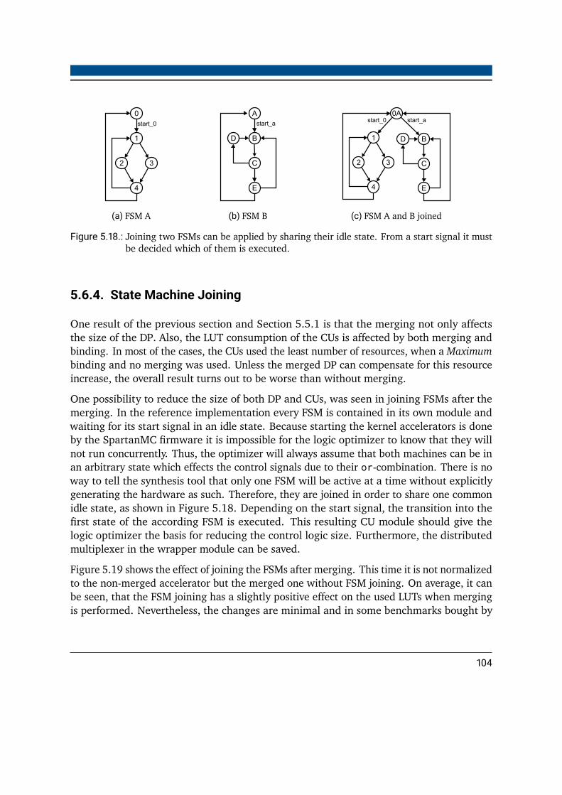
0
1
4
32
start_0
(a) FSM A
A
B
E
C
D
start_a
(b) FSM B
B
E
C
D
0A
1
4
32
start_0 start_a
(c) FSM A and B joined
Figure 5.18.: Joining two FSMs can be applied by sharing their idle state. From a start signal it mustbe decided which of them is executed.
5.6.4. State Machine Joining
One result of the previous section and Section 5.5.1 is that the merging not only affectsthe size of the DP. Also, the LUT consumption of the CUs is affected by both merging andbinding. In most of the cases, the CUs used the least number of resources, when a Maximumbinding and no merging was used. Unless the merged DP can compensate for this resourceincrease, the overall result turns out to be worse than without merging.
One possibility to reduce the size of both DP and CUs, was seen in joining FSMs after themerging. In the reference implementation every FSM is contained in its own module andwaiting for its start signal in an idle state. Because starting the kernel accelerators is doneby the SpartanMC firmware it is impossible for the logic optimizer to know that they willnot run concurrently. Thus, the optimizer will always assume that both machines can be inan arbitrary state which effects the control signals due to their or-combination. There is noway to tell the synthesis tool that only one FSM will be active at a time without explicitlygenerating the hardware as such. Therefore, they are joined in order to share one commonidle state, as shown in Figure 5.18. Depending on the start signal, the transition into thefirst state of the according FSM is executed. This resulting CU module should give thelogic optimizer the basis for reducing the control logic size. Furthermore, the distributedmultiplexer in the wrapper module can be saved.
Figure 5.19 shows the effect of joining the FSMs after merging. This time it is not normalizedto the non-merged accelerator but the merged one without FSM joining. On average, it canbe seen, that the FSM joining has a slightly positive effect on the used LUTs when mergingis performed. Nevertheless, the changes are minimal and in some benchmarks bought by
104

0
0.5
1
1.5
2
base
64
dijkst
ra
fletc
her
idct
man
delb
rot
eucli
d
bin
tree
rsa
(2)
jpeg
(4)
aes (3
)
|LU
T| S
ing
leFS
M /
|LU
T| M
ult
iFS
M
none (avg. 1.02)bron-kerbosch (avg. 0.97)
cliquer (avg. 0.99)quick (avg. 0.97)
(a) Normalized LUT utilization. Values <1 are adecrease in resources.
0
0.5
1
1.5
2
base
64
dijkst
ra
fletc
her
idct
man
delb
rot
eucli
d
bin
tree
rsa
(2)
jpeg
(4)
aes (3
)
|REG
| Sin
gle
FSM
/ |
REG
| Mult
iFS
M
none (avg. 1.05)bron-kerbosch (avg. 1.06)
cliquer (avg. 1.04)quick (avg. 1.06)
(b) Normalized register utilization. Values <1are a decrease in resources.
0
0.5
1
1.5
2
base
64
dijkst
ra
fletc
her
idct
man
delb
rot
eucli
d
bin
tree
rsa
(2)
jpeg
(4)
aes (3
)
|DSP| S
ing
leFS
M -
|D
SP| M
ult
iFS
M
nonebron-kerbosch
cliquerquick
(c) Increase of the DSP utilization. Negative val-ues are a decrease.
Figure 5.19.: Hardware resource utilization depending on the clique finding algorithm with joinedFSMs. A small resource decrease can be achieved compared to the not-joined merging.
using more DSPs. When no merging is performed using the None merger, the joining evenaffects the resulting hardware negatively in both LUTs and registers.
5.6.5. Clique Size
So far, merging did not have any benefits over the reference implementation. Using itstimeout, only the Bron-Kerbosch clique finder can be used to spend more computation timeto the end that it finds more or larger cliques. In the previous tests the time limit was30minutes for every merging step. This limit was reasonable because most cases could thenbe merged within less than three hours. To test if the time limit may have been too low, asweep was conducted for all benchmarks with not more than six kernels.
105
Table 5.10 shows the found clique sizes and how many cliques of this size were found at eachstep. For the benchmarks with more than two kernels only the clique of the first mergingstep is shown. Three cases (dijkstra, euclid, and bin tree) can already be skipped for futureevaluation. In all these cases the clique size and the amount of found maximal cliques doesnot change. Furthermore, the clique finder finishes before the given timeout and thus allfound cliques are maximum cliques.
106

Table 5.10.: Clique sizes and the number of found occurrences using the Bron-Kerbosch clique finder with different timelimits. The notation is <amount> x <clique size>.
Time [h:mm]
Benchmark 0:05 0:10 0:15 0:30 1:00 1:30 2:00 3:00base64 1636 x 30 3840 x 30 3840 x 30 4644 x 30 4644 x 30 6096 x 30 – –dijkstra 36 x 14fletcher 508 x 88 314 x 94 432 x 94 432 x 94 864 x 94 1296 x 94 1296 x 94 2808 x 94idct 1 x 1 1 x 1 1 x 1 720 x 169 880 x 169 880 x 169 1132 x 169 2880 x 169mandelbrot 13728 x 28 27456 x 28 6864 x 29 6864 x 29 6864 x 29 27456 x 29 41184 x 29 13728 x 30euclid 4 x 12bin tree 36 x 22
107

0.9
1
1.1
1.2
1.3
1.4
1.5
0 2000 4000 6000 8000 10000 12000
|LU
T| B
ron-K
erb
osc
h /
|LU
T| @
300s
Runtime Limit in [s]
base64fletcher
idctmandelbrot
(a) Normalized LUT utilization.
0.86
0.88
0.9
0.92
0.94
0.96
0.98
1
0 2000 4000 6000 8000 10000 12000
|REG
| Bro
n-K
erb
osc
h /
|R
EG
| @300s
Runtime Limit in [s]
base64fletcher
idctmandelbrot
(b) Normalized register utilization.
-1
-0.5
0
0.5
1
1.5
2
0 2000 4000 6000 8000 10000 12000
|DSP| B
ron-K
erb
osc
h -
|D
SP| @
300s
Runtime Limit in [s]
base64fletcher
idctmandelbrot
(c) Increase of the DSP utilization.
Figure 5.20.: Resource utilization using the Bron-Kerbosch clique finder using different runtimelimits. All benchmarks are normalized to their first test point at 300 s.
Figure 5.20 shows the results for up to three hour time limits. The largest three benchmarkscould not be considered in this test. Not only because the complete merging of 19 kernelswould take approximately nine hours. The Normalized order would have to be used withdifferent CG size thresholds resulting in different numbers of merged DPs. Furthermore, therequired memory amount increases with both CG size and time. After more than one anda half hour, the base64 benchmark failed due to heap space exceedance for example. Theconclusion that can be drawn from this test is rather simple. In most cases, a longer cliquesearch time does not produce better results after synthesis. In two cases, where the testsshow significant differences (idct and mandelbrot) they are again accompanied by changesin the DSP utilization.
108

5.6.6. Merging before Binding
Throughout the last sections, binding was performed before merging. So far, this orderdid not produce results that could compete with the reference solution. To evaluate if thebinding may eventually restrict or narrow later merging possibilities, the order was switched.Without the binding information, the resulting CG is back to regular, as in Figure 5.14a.The test results, which are normalized to the pre-merge binding, are given in Figure 5.21.Because the three merging algorithms overall provide similar results only the QuickCliqueis used due to its runtime advantage over the other two. It is used in combination withthe Normalized order, which only produces multiple DP in the largest benchmarks. FSMswere joined after creating the DP(s). As a comparison, the None merging is also evaluated.In this case, a post-merge binding should not make much of a difference to a pre-mergebinding because there is no inter kernel CR sharing, which can be confirmed. Only slightdeviations from the pre-merge binding variant can be seen and on average they are quasiequal. The merged variant however, performs better in terms of LUTs and not only in caseswhere the DSP utilization increases. A slight increase in register must be traded for that.
0
0.2
0.4
0.6
0.8
1
1.2
1.4
base
64
dijkst
ra
fletc
her
idct
man
delb
rot
eucli
d
bin
tree
rsa
jpeg ae
s
|LU
T| p
ost
-bin
d /
|LU
T| p
re-b
ind
none (avg. 1.00)quick (avg. 0.90)
(a) Normalized LUT utilization.
0
0.2
0.4
0.6
0.8
1
1.2
1.4
base
64
dijkst
ra
fletc
her
idct
man
delb
rot
eucli
d
bin
tree
rsa
jpeg ae
s
|REG
| post
-bin
d /
|R
EG
| pre
-bin
d
none (avg. 1.00)quick (avg. 1.05)
(b) Normalized register utilization.
0
2
4
6
8
10
base
64
dijkst
ra
fletc
her
idct
man
delb
rot
eucli
d
bin
tree
rsa
jpeg ae
s
|DS
P| p
ost
-bin
d -
|D
SP| p
re-b
ind
nonequick
(c) Increase of the DSP usage.
Figure 5.21.: The resource utilization of merged accelerators depends on whether the resourcebinding is done before or after merging.
109

0
0.2
0.4
0.6
0.8
1
1.2
1.4
base
64
dijkst
ra
fletc
her
idct
man
delb
rot
eucli
d
bin
tree
rsa
jpeg ae
s
|LU
T| p
ost
-bin
d /
|LU
T| M
ult
iple
DP
none (avg. 1.03)quick (avg. 1.03)
(a) Normalized LUT Utilization.
0
0.2
0.4
0.6
0.8
1
1.2
1.4
base
64
dijkst
ra
fletc
her
idct
man
delb
rot
eucli
d
bin
tree
rsa
jpeg ae
s
|REG
| post
-bin
d /
|R
EG
| Mult
iple
DP
none (avg. 1.06)quick (avg. 0.99)
(b) Normalized Register Utilization.
0
0.5
1
1.5
2
2.5
3
base
64
dijkst
ra
fletc
her
idct
man
delb
rot
eucli
d
bin
tree
rsa
jpeg ae
s
|DSP| p
ost
-bin
d -
|D
SP| M
ult
iple
DP
nonequick
(c) Increase of the DSP Usage.
Figure 5.22.: Results of post binding normalized to the reference implementation. When the resourcebinding is performed after the merging, it delivers similar results.
These findings, are hard to evaluate when they are only compared to the rather suboptimalbaseline from the previous section. Therefore, they must be held against the original baselineto see, if the post-merge binding has in sum a positive effect in combination with the FSMjoining. This comparison can be seen in Figure 5.22. It can be seen, that the post-mergebinding produces results similar to the reference solution. The None merger has up tonow always shown results close to that range. The QuickClique merged result seems LUTwise extremely close to the None result. A comparison of the resulting CR tables, like 5.9,revealed, that the amount of CRs in the resulting DPs is nearly the same. Although thiscould have been a problem of the merger not finding any cliques because of an incorrectlyconstructed CG, this could be proven to be false. In all cases, maximal cliques of reasonablesizes could be found.
This result allows only one conclusion. Merging before binding increases the inter DPGresource sharings but simultaneously decreases the intra DPG resource sharing. Up tonow the latter one has shown to actually reduce the number of resources as shown inSection 5.5.1. Therefore, this potential should not be neglected in favor of the less effectiveinter DPG resource sharing enabled by the merging.
110
5.7. Conclusion and Outlook
The conclusion that can be drawn from the previous section is not trivial. It could only beshown, that the currently established merging approaches using a CG as an intermediaterepresentation are not directly suitable for fine-grained hardware accelerators. The problemis a many-layered one that apparently cannot be easily reduced to only shared CRs andinterconnects. There are further and non neglectable influences by parts that are not coveredby this view.
The merging would for example have to consider and distinguish between newly addedand already existing multiplexers. Furthermore, as shown in Section 5.5.1 the mergedDP only partially contributes to the result. Also, the control signals that are required toselect multiplexer inputs and enable registers have an influence on the FSM’s resourceconsumption. Therefore, the complete accelerator including its state machine rather thanonly the DPG needs to be modeled.
Instead of single instruction matchabilities the graph would have to be focused more oncombinations of instructions. Modeling the shared interconnections between instructions inthe CG is a first step towards this but seems not yet to be enough. Finding structures ofmultiple (≈ 5 to 10) instructions in one DPG that have a very similar counterpart would bethe next step.
All the above mentioned considerations can most likely be modeled in a CG. Either byinserting pseudo compatibility nodes, similar to the ECNs or by weighting. For complexcontexts, weighting the edges of the CG instead of nodes can be used. The maximumclique search then turns into the MEWC problem for which approaches already exist [51].However, despite the feasibility of modeling the problem there is still the question ofsolvability. The experiments have shown that even basic CGs without weighting or multiinstruction pseudonodes can grow too big. Solving for the maximum (node) weight insteadof the maximum size showed runtime penalties of a factor of 1000. This further reducesthe problem size that is still tractable. As the number of edges in a CG is even higher, theMEWC will again add to that.
When the CG sizes are in a range where the clique finding becomes insoluble due to time ormemory limits, the CG has one big disadvantage. The higher the similarity is between twoDPGs the larger the CG becomes. Thus, the most interesting cases where the most CRs andinterconnects can be reused become intractable. To overcome this problem, approaches likethe Normalized merging order, can avoid too large CGs. This however, results in mergingDPGs that are less similar to each other instead of the most interesting pairs.
111
6. General Conclusion
As each of the case studies already has their own conclusion, this chapter gives a shortsummary. Furthermore, a few words have to be said about the CG based merging approachin general.
In Chapter 4 the goal was to implement an analysis system that is tailored to the user’s needs.A set of sample problems in form of assertions was used to generate a runtime reconfigurableplatform. The focus of this part was to enable a quick adaptability to new problems forshort turnaround times. The DP merging approach using CGs performed well on differentreal world examples. Similar structures of operations could be found between DPs. Whenmultiple input problems are merged into one, the amount of possible configurations is notonly limited to the input problems themselves. Every CE introduces new paths throughthe DP and thus, creates a vast room of options. Both presented mapping algorithms makeuse of these to find configurations for problems that were not known during the merging -provided that all required resources are available.
Chapter 5 revealed that the CG approach can fail to achieve its goals. Obtaining anyresource reductions by reusing CRs in time multiplexed setups is more complicated than itappears at first. Only considering operations and the data flow between them is not enoughinformation. It would have to model more complex relations between operations, operands’registers, and their controlling parts. Although the merging finds resources, and even wholestructures that are equal, the penalties outweigh the benefits. This is caused by the factthat multiplexers introduce overheads that are in some cases bigger than the operationsthey share. Resource sharing has to be applied on coarser structures rather than singleoperations.
Lessons Learned One finding that originated from the runtime reconfiguration applicationwas the importance of a well performing compiler. The TeSSLa compiler produces CDPGsthat are agnostic of the steps that have to be performed afterwards. As stated in Section 4.8it is recommendable to have operations arranged in a fixed order whenever applicable.Such a quasi-canonification can greatly increase chances that later mapping new CDPGs is
112

possible. Detecting sections that implement the same functionality but can be written indifferent ways, can also reduce the required resources during merging.
During the work on the projects, two problems occured frequently. The first one is thesize of the generated CGs. Even tools that are known to deliver good results in polynomialtime were not able to terminate within a reasonable amount of time. Especially, the mostinteresting cases, where two input problems barely differ, have shown to produce the largestCGs. Having an algorithm that is supposed to find similarities but performs worst in termsof runtime, when the input problems are very similar is somehow counterproductive.
Nevertheless, the term compatibility and CGs themselves are an important construct. Takingthe experience from the two case studies into account they should just not be used as astandalone solutions. For large problems a different approach must be found that worksmore locally oriented than the presented one. The CG tries to get a global view of theproblem. This may already overstate it, as the locality of operations also plays a role. TheCGs can still be an additional tool to make decisions, but only for a very limited window ofthe complete problem. This would further allow to enrich it with information like multiplexeroverhead or register sharing options.
Proposals As with all problems, there is an infinite amount of solutions to solve them.Nevertheless, three promising approaches shall be mentioned here.
• Operation clustersOne way to reduce the problem size, or more specifically the CG size, is to not addevery matchable instruction/operation. When resource reduction is the goal and theydo not have predecessors or successors that can be matched as well, they do not haveany benefit. It is more advisable to locally search for common predecessors in bothgraphs and add them as a cluster. Operations that are not part of a cluster of at leastfive instructions for example are not added to the CG. A higher minimum clusterrequirement will strongly reduce the number of nodes in the CG but each of them hasa higher value. Choosing the cluster size dynamically based on the input DPGs thenenables the most interesting cases. When two DPGs are essentially equal, the clusterswill be large and the CG will be small. This metric also allows deciding which DPGsare worth merging or which ones to merge first. This is interesting for both runtimereconfiguration and resource reduction. It is also conceivable to use this approachwithout generating a CG. After finding all matching clusters for a node one can applya greedy algorithm. Selecting the largest cluster first and discarding incompatibleones possibly leads to good or at least acceptable results.
113

• Divide and conquerA classic way to reduce the problem size is to split it into smaller ones and solve thesesubproblems subsequently. This can also be applied for the clique problem. The firstCG would be constructed from only a subset of the operations of both accelerators.After the clique search is applied, all other incompatible nodes are removed from theCG. Then, new operations can be added to contribute to the CG. When only new nodesare allowed that do not contradict the already found clique, its nodes can be removed.Although the clique problem must be solved multiple times it may still be beneficialas the runtime is much shorter. A possible but rather coarse split is to consider onlyECNs in the first step and add the NCNs afterwards. The second step can be furtherseparated when the NCNs are added according to their type because incompatibilitiesonly occur within it.
• A different focusThe last proposal, which targets the hardware accelerators, is to construct the CG fromdifferent information. Instead of operations their operands can be used to generateit. Lots of multiplexing has to be done in order to store the output of the correctoperation into a register. When operands share the same source operations and theyare placed into the same register, these can be omitted. Furthermore, it has a positiveside-effect on the problem size. As there are always more operations than operandsin an accelerator’s DPG, the resulting CGs will smaller.
114

Bibliography
[1] W. Luk, N. Shirazi, and P. Y. K. Cheung. “Compilation tools for run-time reconfigurabledesigns”. In: Proceedings. The 5th Annual IEEE Symposium on Field-ProgrammableCustom Computing Machines Cat. No.97TB100186). Apr. 1997, pp. 56–65 (cit. onp. 3).
[2] N. Shirazi, W. Luk, and P. Y. K. Cheung. “Automating production of run-time recon-figurable designs”. In: Proceedings. IEEE Symposium on FPGAs for Custom ComputingMachines (Cat. No.98TB100251). Apr. 1998, pp. 147–156 (cit. on p. 3).
[3] Nahri Moreano et al. “Datapath merging and interconnection sharing for reconfig-urable architectures”. In: Proceedings of the 15th international symposium on SystemSynthesis - ISSS ’02 (2002) (cit. on pp. 3, 9, 11).
[4] N. Moreano et al. “Efficient datapath merging for partially reconfigurable architec-tures”. In: IEEE Transactions on Computer-Aided Design of Integrated Circuits andSystems 24.7 (July 2005), pp. 969–980. issn: 0278-0070 (cit. on pp. 3, 9, 11, 13,14).
[5] Mahmood Fazlali et al. “A New Datapath Merging Method for Reconfigurable System”.In: Reconfigurable Computing: Architectures, Tools and Applications (2009), pp. 157–168. issn: 1611-3349 (cit. on pp. 3, 9).
[6] M. Fazlali et al. “High speed merged-datapath design for run-time reconfigurable sys-tems”. English. In: 2009 International Conference on Field-Programmable Technology.Dec. 2009, pp. 339–343 (cit. on p. 3).
[7] M. Stojilovic et al. “Selective flexibility: Breaking the rigidity of datapath merging”.In: 2012 Design, Automation & Test in Europe Conference & Exhibition (DATE) (Mar.2012) (cit. on p. 3).
[8] S. C. Goldstein et al. “PipeRench: a coprocessor for streaming multimedia accelera-tion”. In: Proceedings of the 26th International Symposium on Computer Architecture(Cat. No.99CB36367). 1999, pp. 28–39 (cit. on p. 4).
[9] Venkatraman Govindaraju, Chen-Han Ho, and Karthikeyan Sankaralingam. “Dynam-ically Specialized Datapaths for energy efficient computing”. In: 2011 IEEE 17thInternational Symposium on High Performance Computer Architecture (Feb. 2011)(cit. on p. 4).
115

[10] D. L. Wolf et al. “AMIDAR Project: Lessons Learned in 15 Years of ResearchingAdaptive Processors”. In: 2018 13th International Symposium on ReconfigurableCommunication-centric Systems-on-Chip (ReCoSoC). July 2018, pp. 1–8 (cit. on p. 4).
[11] M Grötschel, L Lovász, and A Schrijver. “Relaxations of vertex packing”. In: Journalof Combinatorial Theory, Series B 40.3 (June 1986), pp. 330–343 (cit. on p. 8).
[12] Martin Grötschel, László Lovász, and Alexander Schrijver. Geometric Algorithms andCombinatorial Optimization. Springer Berlin Heidelberg, 1988 (cit. on pp. 8, 17).
[13] Jürgen Teich and Christian Haubelt. Digitale Hardware/Software-Systeme. Springer-Verlag GmbH, Mar. 2, 2007. isbn: 3540468226 (cit. on p. 9).
[14] Patric R. J. Östergård. “A Fast Algorithm for the Maximum Clique Problem”. In:Discrete Appl. Math. 120.1-3 (Aug. 2002), pp. 197–207. issn: 0166-218X (cit. onpp. 14, 21, 80).
[15] Donald J. Rose, R. Endre Tarjan, and George S. Lueker. “Algorithmic Aspects ofVertex Elimination on Graphs”. In: SIAM Journal on Computing 5.2 (June 1976),pp. 266–283 (cit. on p. 17).
[16] Philipp Käsgen. “Method for Finding Maximal Cliques in Compatibility Graphs”.Master Thesis. TU Darmstadt, Sept. 15, 2016 (cit. on pp. 19, 20).
[17] Philip Gottschling and Christian Hochberger. “ReEP: A Toolset for Generation andProgramming of Reconfigurable Datapaths for Event Processing”. In: 2017 IEEEInternational Parallel and Distributed Processing Symposium Workshops (IPDPSW).IEEE, May 2017 (cit. on pp. 20, 22, 29).
[18] DIMACS benchmark set. url: http : / / iridia . ulb . ac . be / ~fmascia /maximum_clique/DIMACS-benchmark (visited on 11/12/2019) (cit. on pp. 21,97).
[19] Normann Decker et al. “Rapidly Adjustable Non-intrusive Online Monitoring forMulti-core Systems”. In: Lecture Notes in Computer Science. Springer InternationalPublishing, 2017, pp. 179–196 (cit. on p. 22).
[20] Normann Decker et al. “Online analysis of debug trace data for embedded systems”.In: 2018 Design, Automation & Test in Europe Conference & Exhibition (DATE). IEEE,Mar. 2018 (cit. on p. 22).
[21] Jean Souyris et al. “Formal Verification of Avionics Software Products”. In: FM 2009:Formal Methods. Ed. by Ana Cavalcanti and Dennis R. Dams. Berlin, Heidelberg:Springer Berlin Heidelberg, 2009, pp. 532–546. isbn: 978-3-642-05089-3 (cit. onp. 22).
116

[22] Andreas Bauer and Martin Leucker. “The Theory and Practice of SALT”. In: NASAFormal Methods (2011), pp. 13–40. issn: 1611-3349 (cit. on p. 23).
[23] Stefan Klir. “Automatic Code Instrumentation for Minimal Invasive, Hardware Sup-ported Runtime Verification”. Master Thesis. TU Darmstadt, June 30, 2017 (cit. onp. 24).
[24] Xilinx. Zynq-7000 SoC Data Sheet: Overview. Ed. by Xilinx. July 2, 2018 (cit. on pp. 25,68).
[25] ARM Ltd. CoreSight™ Program Flow Trace™ PFTv1.0 and PFTv1.1 Architecture Specifi-cation IHI 0035B. 2011 (cit. on p. 25).
[26] ARM Ltd. ARM® Embedded Trace Macrocell Architecture Specification - ETMv4.0 toETMv4.2 - IHI 0064D. 2016 (cit. on p. 25).
[27] RAPTIA Systems. Continuous tracing with the RTBx data logger. url: https://www.rapitasystems.com/system/files/downloads/mc-pb-301_rtbx_product_brief_v4.pdf (visited on 11/12/2019) (cit. on p. 26).
[28] Alexander Weiss and Alexander Lange. “Trace-Data Processing and Profiling Device”.US Patent 9286186B2. 2016 (cit. on p. 27).
[29] Gerald Hempel and Christian Hochberger. “A resource optimized Processor Core forFPGA based SoCs”. In: 10th Euromicro Conference on Digital System Design Architec-tures, Methods and Tools (DSD 2007) (Aug. 2007) (cit. on pp. 29, 68).
[30] FTDI. FT2232H Dual High Speed USB to Multipurpose UART/FIFO IC. Ed. by FutureTechnology Devices International Ltd. (cit. on p. 29).
[31] Martin Leucker et al. “TeSSLa: Runtime Verification of Non-synchronized Real-TimeStreams”. In: Proceedings of the 33rd Annual ACM Symposium on Applied Computing -SAC ’18. ACM Press, 2018 (cit. on p. 30).
[32] Andreas Harder. “Development of a Trace Based Instruction Reconstruction HardwareModule”. Bachelor Thesis. TU Darmstadt, Nov. 4, 2019 (cit. on p. 34).
[33] Steffen Grimm. “Automatische Superposition von Datenpfaden auf Basis von Kom-patibilitätsgraphen”. Bachelor Thesis. TU Darmstadt, June 11, 2016 (cit. on p. 46).
[34] John E. Hopcroft and Richard M. Karp. “An n5/2 Algorithm for Maximum Matchingsin Bipartite Graphs”. In: SIAM Journal on Computing 2.4 (Dec. 1973), pp. 225–231.issn: 1095-7111 (cit. on p. 48).
[35] SCPSolver - an easy to use Java Linear Programming Interface. url: http://www.scpsolver.org (visited on 11/12/2019) (cit. on p. 53).
117
[36] GLPK (GNU Linear Programming Kit). url: https://www.gnu.org/software/glpk (visited on 11/12/2019) (cit. on p. 53).
[37] Package ’lpSolve’. Aug. 19, 2019. (Visited on 11/12/2019) (cit. on p. 53).[38] Coen Bron and Joep Kerbosch. “Algorithm 457: finding all cliques of an undirected
graph”. In: Commun. ACM 16.9 (Sept. 1973), pp. 575–577. issn: 0001-0782 (cit. onpp. 60, 80).
[39] Xilinx. MicroBlaze Micro Controller System v3.0. Dec. 20, 2017 (cit. on p. 67).[40] Intel. Nios II Processor Reference Guide. Oct. 17, 2019 (cit. on p. 67).[41] Markus Vogt et al. “GCC-Plugin for Automated Accelerator Generation and Integration
on Hybrid FPGA-SoCs”. In: Proceedings of the Second International Workshop on FPGAsfor Software Programmers (FSP). FSP 2015. Sept. 2015 (cit. on p. 68).
[42] Gerald Hempel. “Generation of Application Specific Hardware Extensions for HybridArchitechtures”. PhD thesis. Dresden University of Technology, Faculty of ComputerScience, Dec. 20, 2017 (cit. on pp. 68, 70, 79).
[43] J. Rohde and C. Hochberger. “Using GCC Analysis Techniques to Enable ParallelMemory Accesses in HLS”. In: FSP 2017; Fourth International Workshop on FPGAs forSoftware Programmers. Sept. 2017, pp. 1–8 (cit. on p. 68).
[44] Johanna Rohde and Christian Hochberger. “AutoBoxing: Improving GCC Passes toOptimize HW/SW Multi-Versioning of Kernels for HLS”. In: International Conferenceon Field-Programmable Technology (ICFPT). Dec. 11, 2019, pp. 319–322. isbn: 978-1-7281-2943-3 (cit. on p. 68).
[45] Digilent. Nexys Video™ FPGA Board Reference Manual. Ed. by Digilent. July 27, 2017(cit. on p. 69).
[46] Tom Feist. Vivado Design Suite. June 22, 2012 (cit. on p. 69).[47] ECMA. The JSON Data Interchange Syntax. Ed. by ECMA International. Dec. 2017
(cit. on p. 70).[48] Mahmood Fazlali, Ali Zakerolhosseini, and Georgi Gaydadjiev. “A Modified Merging
Approach for Datapath Configuration Time Reduction”. In: Reconfigurable Computing:Architectures, Tools and Applications (2010), pp. 318–328. issn: 1611-3349 (cit. onp. 87).
[49] M. Fazlali, A. Zakerolhosseini, and G. Gaydadjiev. “Efficient datapath merging forthe overhead reduction of run-time reconfigurable systems”. In: J Supercomput 59.2(June 2010), pp. 636–657. issn: 1573-0484 (cit. on p. 87).
118

[50] Y. Hara-Azumi et al. “Selective Resource Sharing with RT-Level Retiming for ClockEnhancement in High-Level Synthesis”. In: 2012 IEEE 14th International Conferenceon High Performance Computing and Communication 2012 IEEE 9th InternationalConference on Embedded Software and Systems. June 2012, pp. 1534–1540 (cit. onp. 88).
[51] Seyedmohammadhossein Hosseinian et al. “The Maximum Edge Weight Clique Prob-lem: Formulations and Solution Approaches”. In: Optimization Methods and Applica-tions : In Honor of Ivan V. Sergienko’s 80th Birthday. Ed. by Sergiy Butenko, Panos M.Pardalos, and Volodymyr Shylo. Cham: Springer International Publishing, 2017,pp. 217–237. isbn: 978-3-319-68640-0 (cit. on p. 111).
119
A. Appendix
A.1. Event Vector
The event messages can have different causes that are encoded in its Type field. Possibletypes are:
• Application Messages (APP)are sent explicitly by the user by sending data to the ITM in the software.
• Data Messages (DATA)indicate read or write access on the processors data bus. Usually they are only sentfor a small address window of interest to not flood the trace interface.
• State Changes (ST_CHG)are sent whenever an exception is entered or exited, or the processor is halted.
• Register Changes (REG_CHG)are mainly used to indicate thread changes (change of the context ID). However, it isnot the only function.
• Trigger Messages (TRIG)indicate that a watchpoint was hit.
• Error Messages (ERR)can for example indicate an overflow of the processor’s internal trace buffer.
• Instruction Reconstruction Messages (IR)carry information about last executed WPs.
Depending on the type, the dynamic data has different meanings that are given in Table A.1.
120

Table A.1.: Overview over the different event packages that can be generated by the trace prepro-cessing stage. Numbers in brackets indicate the field’s bit width.
APP DATA ST_CHG REG_CHG TRIG ERR IRID (32) Type (1) ID (32) ID (32) ID (32) ID (32) ID (32)
Value (32) Size (3) Value (32) Value (32) Value (32) Value (32) ∆Timestamp (32)TimestampValid (1)
Address (32) – – – – TimestampValid (1)Value (32)
121

122

A.2. Simulation of the Event Processor
Figure A.1.: Simulation of the EP from Figure 4.8.
123
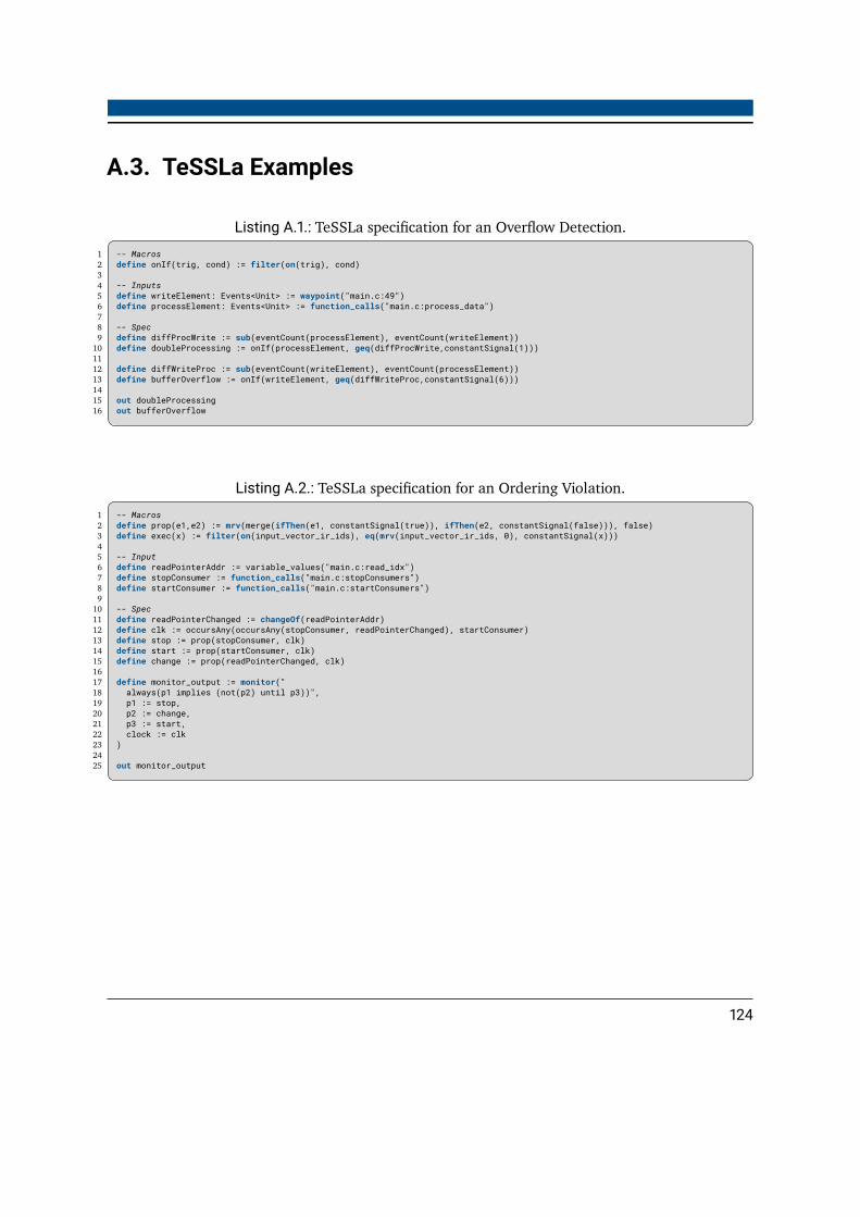
A.3. TeSSLa Examples
Listing A.1.: TeSSLa specification for an Overflow Detection.1 -- Macros2 define onIf(trig, cond) := filter(on(trig), cond)34 -- Inputs5 define writeElement: Events<Unit> := waypoint("main.c:49")6 define processElement: Events<Unit> := function_calls("main.c:process_data")78 -- Spec9 define diffProcWrite := sub(eventCount(processElement), eventCount(writeElement))
10 define doubleProcessing := onIf(processElement, geq(diffProcWrite,constantSignal(1)))1112 define diffWriteProc := sub(eventCount(writeElement), eventCount(processElement))13 define bufferOverflow := onIf(writeElement, geq(diffWriteProc,constantSignal(6)))1415 out doubleProcessing16 out bufferOverflow
Listing A.2.: TeSSLa specification for an Ordering Violation.1 -- Macros2 define prop(e1,e2) := mrv(merge(ifThen(e1, constantSignal(true)), ifThen(e2, constantSignal(false))), false)3 define exec(x) := filter(on(input_vector_ir_ids), eq(mrv(input_vector_ir_ids, 0), constantSignal(x)))45 -- Input6 define readPointerAddr := variable_values("main.c:read_idx")7 define stopConsumer := function_calls("main.c:stopConsumers")8 define startConsumer := function_calls("main.c:startConsumers")9
10 -- Spec11 define readPointerChanged := changeOf(readPointerAddr)12 define clk := occursAny(occursAny(stopConsumer, readPointerChanged), startConsumer)13 define stop := prop(stopConsumer, clk)14 define start := prop(startConsumer, clk)15 define change := prop(readPointerChanged, clk)1617 define monitor_output := monitor("18 always(p1 implies (not(p2) until p3))",19 p1 := stop,20 p2 := change,21 p3 := start,22 clock := clk23 )2425 out monitor_output
124
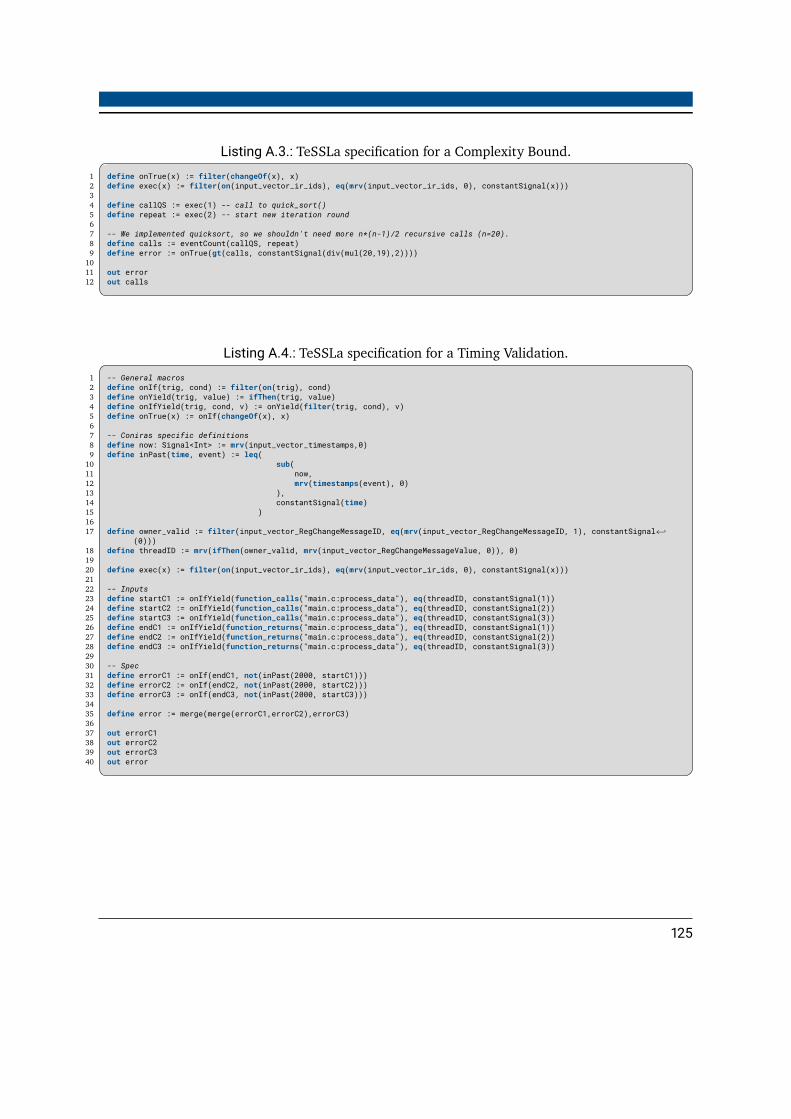
Listing A.3.: TeSSLa specification for a Complexity Bound.1 define onTrue(x) := filter(changeOf(x), x)2 define exec(x) := filter(on(input_vector_ir_ids), eq(mrv(input_vector_ir_ids, 0), constantSignal(x)))34 define callQS := exec(1) -- call to quick_sort()5 define repeat := exec(2) -- start new iteration round67 -- We implemented quicksort, so we shouldn't need more n*(n-1)/2 recursive calls (n=20).8 define calls := eventCount(callQS, repeat)9 define error := onTrue(gt(calls, constantSignal(div(mul(20,19),2))))
1011 out error12 out calls
Listing A.4.: TeSSLa specification for a Timing Validation.1 -- General macros2 define onIf(trig, cond) := filter(on(trig), cond)3 define onYield(trig, value) := ifThen(trig, value)4 define onIfYield(trig, cond, v) := onYield(filter(trig, cond), v)5 define onTrue(x) := onIf(changeOf(x), x)67 -- Coniras specific definitions8 define now: Signal<Int> := mrv(input_vector_timestamps,0)9 define inPast(time, event) := leq(
10 sub(11 now,12 mrv(timestamps(event), 0)13 ),14 constantSignal(time)15 )1617 define owner_valid := filter(input_vector_RegChangeMessageID, eq(mrv(input_vector_RegChangeMessageID, 1), constantSignal←↩
(0)))18 define threadID := mrv(ifThen(owner_valid, mrv(input_vector_RegChangeMessageValue, 0)), 0)1920 define exec(x) := filter(on(input_vector_ir_ids), eq(mrv(input_vector_ir_ids, 0), constantSignal(x)))2122 -- Inputs23 define startC1 := onIfYield(function_calls("main.c:process_data"), eq(threadID, constantSignal(1))24 define startC2 := onIfYield(function_calls("main.c:process_data"), eq(threadID, constantSignal(2))25 define startC3 := onIfYield(function_calls("main.c:process_data"), eq(threadID, constantSignal(3))26 define endC1 := onIfYield(function_returns("main.c:process_data"), eq(threadID, constantSignal(1))27 define endC2 := onIfYield(function_returns("main.c:process_data"), eq(threadID, constantSignal(2))28 define endC3 := onIfYield(function_returns("main.c:process_data"), eq(threadID, constantSignal(3))2930 -- Spec31 define errorC1 := onIf(endC1, not(inPast(2000, startC1)))32 define errorC2 := onIf(endC2, not(inPast(2000, startC2)))33 define errorC3 := onIf(endC3, not(inPast(2000, startC3)))3435 define error := merge(merge(errorC1,errorC2),errorC3)3637 out errorC138 out errorC239 out errorC340 out error
125
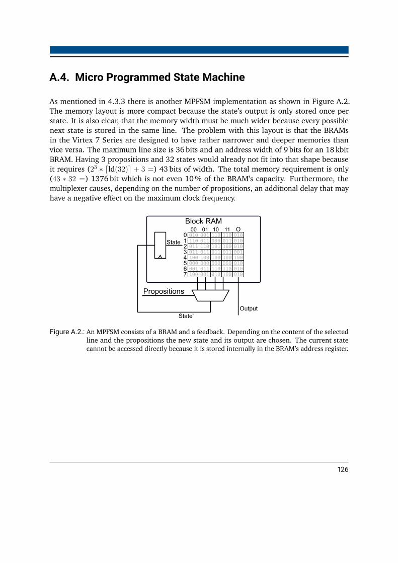
A.4. Micro Programmed State Machine
As mentioned in 4.3.3 there is another MPFSM implementation as shown in Figure A.2.The memory layout is more compact because the state’s output is only stored once perstate. It is also clear, that the memory width must be much wider because every possiblenext state is stored in the same line. The problem with this layout is that the BRAMsin the Virtex 7 Series are designed to have rather narrower and deeper memories thanvice versa. The maximum line size is 36 bits and an address width of 9 bits for an 18 kbitBRAM. Having 3 propositions and 32 states would already not fit into that shape becauseit requires (23 ∗ ⌈ld(32)⌉ + 3 =) 43 bits of width. The total memory requirement is only(43 ∗ 32 =) 1376 bit which is not even 10% of the BRAM’s capacity. Furthermore, themultiplexer causes, depending on the number of propositions, an additional delay that mayhave a negative effect on the maximum clock frequency.
01
Block RAM
State'
Propositions
Output
00 10 11 O01234567
010010 001 110 110010110 011 000 011010011 110 101 100001011 011 011 011100100 100 100 100010000 000 000 000010001 011 110 110010100 001 010 100
State
Figure A.2.: An MPFSM consists of a BRAM and a feedback. Depending on the content of the selectedline and the propositions the new state and its output are chosen. The current statecannot be accessed directly because it is stored internally in the BRAM’s address register.
126
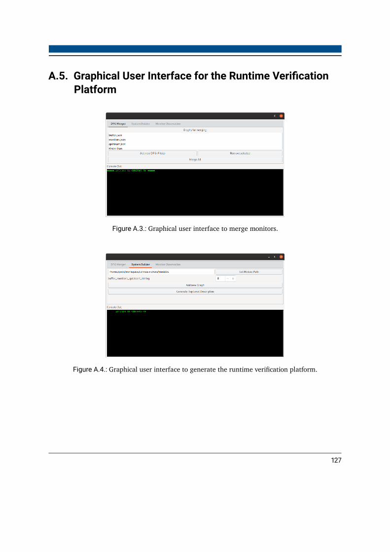
A.5. Graphical User Interface for the Runtime VerificationPlatform
Figure A.3.: Graphical user interface to merge monitors.
Figure A.4.: Graphical user interface to generate the runtime verification platform.
127

Figure A.5.: Graphical user interface to initialize observing monitors.
Figure A.6.: Graphical user interface to observe running monitors.
128

A.6. File Formats
Listing A.5.: Resource table for a hardware accelerator1 # Operator, Bit Width, Signed, Amount2 GreaterThan, 9, true, 1503 Memory, 18, false, 14 ShiftLeft, 18, false, 105 Mult, 9, true, 106 GreaterThan, 9, false, 1507 GreaterThan, 18, true, 1508 Mult, 9, false, 109 GreaterThan, 18, false, 150
10 Div, 9, true, 111 Add, 18, false, 15012 And, 18, false, 15013 Or, 18, false, 15014 Xor, 18, false, 15015 Sub, 18, false, 15016 Div, 18, true, 117 Div, 9, false, 118 Add, 9, false, 15019 And, 9, false, 15020 Or, 9, false, 15021 Xor, 9, false, 15022 Sub, 9, false, 15023 GreaterEqual, 9, false, 15024 NotEqual, 18, false, 15025 GreaterEqual, 9, true, 15026 NotEqual, 9, false, 15027 Equal, 18, false, 15028 Mult, 18, true, 1029 ShiftLeft, 9, false, 1030 Equal, 9, false, 15031 GreaterEqual, 18, false, 15032 Mult, 18, false, 1033 GreaterEqual, 18, true, 150
129

Listing A.6.: Excerpt of the JSON format for hardware accelerator export.
1 {2 "@type":"de.tu_darmstadt.rs.gcc_datapath_merging.←↩
statemachine.StateMachine",3 "resources":[4 {5 "@id":1028,6 "@type":"de.….resource.AddResource",7 "bitWidth":18,8 "isSigned":"false"9 },
10 …11 ],12 "idleState":{"@ref":1000},13 "inputs":[14 {15 "@type":"de.….IoOperand",16 "@id":1031,17 "offset":2,18 "bitWidth":18,19 "isSigned":"true",20 "name":"base64_dec_map_000",21 "spmcuid":"1244000"22 },23 …24 ],25 "outputs":[26 {27 "@type":"de.….IoOperand",28 "@id":1036,29 "offset":7,30 "bitWidth":18,31 "isSigned":"false",32 "name":"p_53_053",33 "spmcuid":"1278053"34 },35 …36 ],37 "states":[38 {39 "@type":"de.….State",40 "@id":1002,41 "stateNumber":2,42 "basicBlock":22,43 "isStart":"false",44 "liveIn":[45 {"@ref":1037},46 …47 ],48 "liveOut":[49 {50 "@type":"de.….Operand",51 "@id":1052,
52 "bitWidth":9,53 "isSigned":"false",54 "name":"tmp_15_015",55 "spmcuid":"15"56 },57 {"@ref":1037},58 …59 ],60 "transitions":[61 {62 "@type":"de.….Transition",63 "registered":"false",64 "nextState":{"@ref":1002},65 "branchOn":"false",66 "branchOperand":{"@ref":1051}67 },68 {69 "@type":"de.….Transition",70 "nextState":{"@ref":1003}71 },72 ],73 "instructions":[74 {75 "@type":"de.….instruction.IfElseInstruction",76 "inputOperands":[77 {"@ref":1051}78 ],79 "trueInstructions":[80 {81 "@type":"de.….instruction.←↩
MemReadDataInstruction",82 "isLong":"false",83 "accessId":1,84 "accessBytes":1,85 "outputOperand":{"@ref":1052},86 "outputLow":null,87 "outputWidth":9,88 "isSigned":"false",89 "assignedResource":null90 },91 ],92 "falseInstructions":[93 ],94 "unregisteredOperands":[95 096 ]97 },98 …99 ]
100 }101 ]102 }
Listing A.7.: Periphery map file for hardware accelerators.1 #accelerator name absolute address address offset2 main_0001_base64_encode 3F800 03 main_0001_base64_decode 3F814 14
130