Md Ranju Sardar - DUET
130
DESIGN AND DEVELOPMENT OF MICROCONTROLLER BASED SYSTEM FOR GENERATION, TRANSMISSION AND RECEPTION OF DIGITAL ENERGY METER READING USING SMS TECHNOLOGY Md Ranju Sardar DEPARTMENT OF ELECTRICAL & ELECTRONIC ENGINEERING DHAKA UNIVERSITY OF ENGINEERING AND TECHNOLOGY, GAZIPUR January 2012
-
Upload
khangminh22 -
Category
Documents
-
view
4 -
download
0
Transcript of Md Ranju Sardar - DUET

DESIGN AND DEVELOPMENT OF MICROCONTROLLER BASED
SYSTEM FOR GENERATION, TRANSMISSION AND RECEPTION
OF DIGITAL ENERGY METER READING USING SMS
TECHNOLOGY
Md Ranju Sardar
DEPARTMENT OF ELECTRICAL & ELECTRONIC ENGINEERING
DHAKA UNIVERSITY OF ENGINEERING AND TECHNOLOGY,
GAZIPUR
January 2012

ii
DESIGN AND DEVELOPMENT OF MICROCONTROLLER BASED
SYSTEM FOR GENERATION, TRANSMISSION AND RECEPTION
OF DIGITAL ENERGY METER READING USING SMS
TECHNOLOGY
A thesis
submitted to the Department of Electrical and Electronic
Engineering DUET, Gazipur in partial completion of the
requirements for the degree of
MASTER OF SCIENCE IN ELECTRICAL AND ELECTRONIC
ENGINEERING
by
Md Ranju Sardar
Under supervision of
Dr. Md. Bashir Uddin
Professor & Head
DEPARTMENT OF ELECTRICAL & ELECTRONIC ENGINEERING DHAKA UNIVERSITY OF ENGINEERING AND TECHNOLOGY,
GAZIPUR
January 2012

iii

iv

v
ACKNOWLEDGEMENTS
I would like to express my appreciation and reflective thanks to my supervisor
Professor, Dr.Md Bashir Uddin, Head, Department of Electrical and Electronic
Engineering of Dhaka University of Engineering and Technology Gazipur for his
authentic direction, encouragement and cooperative support whole over my thesis
work. I am grateful to Assistant Professor Mohammad shazzat Hossain, Department
of Electrical and Electronic Engineering of Dhaka University of Engineering and
Technology Gazipur.I would also like to express my gratefulness and in particular
thanks to Md Abdul Mannan, Professor and Dean, Department of Electrical and
Electronic Engineering of Dhaka University of Engineering and Technology Gazipur
his cordial help and valuable suggestions. I would like to thank my parents and elder
brothers for their regular encouragements. I would like to get across my furthermost
gratitude towards Dr Md Anawarul Abedin, Associate professor, Department of
Electrical and Electronic Engineering of Dhaka University of Engineering and
Technology Gazipur for his Logitech support throughout this research work. I am
grateful to all of my colleagues and friends. I am also grateful to the librarian and all
the sets up of Dhaka University of Engineering and Technology for their back up.
January 2012 Md. Ranju Sardar

vi
ABSTRACT
The main objective of this thesis is to generate, transmit and receive the digital energy
meter reading into database server using SMS Technology. In fact the over all system
is divided into two units such as one is SMS message transmitting unit and another is
SMS message receiving unit. The SMS message transmitting unit consists of
microcontroller, energy measuring chip (EMC), GSM (Global System for mobile
communication) module, SIM (Subscriber Identification Module) and LCD display.
Consequently SMS message receiving unit consists of GSM modem, PC (Personal
Computer), SMS Enabler Software, SQL (Structured, Query Language) and database
server. In case of SMS message transmitting unit, microcontroller is interfaced with
energy measuring chip, GSM module and LCD display. In this system
microcontroller is used for controlling the interfacing equipment functions, data
reading, calculation, storage and display the meter reading on LCD display. The
microcontroller accumulates reading over a month and at the first moment of a month
the microcontroller sends the meter reading to GSM module. The GSM module
receives the corresponding reading from microcontroller, produces short message
based on the data reading and sends the message through mobile communication
systems. Lastly the meter reading is saved into database server via mobile
communication systems, GSM modem, SMS Enabler Software and SQL (Structured
Query Language). The system will play an important role to provide proper service to
the consumers by reducing cost, system loss and corruption and increasing reputation
of the organization. The introduction of the system helps maintain accuracy and make
friendly relationship between consumers and organization.

vii
CONTENTS
Pages Board of Examiners iii Declaration iv Acknowledgement v Abstract vi References xi Appendices xi Use of program xi List of Table xi List of Figures xiii Abbreviations xv
CHAPTER-1
INTRODUCTION
1.1 Back Ground of the Work 1 1.2 Present State of Art of Microcontroller Based System 3 1.2.1 System Architecture 3 1.2.1.1 Remote Meter 4 1.2.1.2 Central Server 6 1.3 Fundamental Terms Related to SMS Mode Meter Reading
System 8
1.3.1 Global System for Mobile Communication (GSM ) 9 1.3.2 GSM Frequencies 9 1.3.3 Short Message Service (SMS) 10 1.3.4 Microcontroller 10 1.3.5 PIC (Peripheral Interface Controller) 11 1.3.6 GSM Module and Modem 11 1.3.7 Subscriber Identity Module (SIM) 11 1.3.8 Digital Energy Meter 12 1.3.9 LCD (Liquid Crystal Display) 13 1.3.10 PICBASIC PRO Software 13 1.3.11 EPIC Win 14 1.3.12
SMS Enabler Software 14
1.3.13 SQL(Structured Query Language) 15 1.4 Objectives 15 1.5 Organization of the Thesis 15

viii
CHAPTER-2 GSM AND SMS TECHNOLOGY
2.1 Introduction 17 2.2 SMS as a Part of GSM 17 2.2.1 Initial Concept 17 2.2.2 Early Development 18 2.2.3 Early Implementation 19 2.2.4 Text Messing Outside GSM 20 2.2.5 SMS Today 20 2.2.6 Message Size 20 2.3 SMS Protocols 21 2.4 Network Reference Model for SMS 22 2.5 How Does SMS Work 23 2.6 Benefit of SMS 25 2.7 Application of SMS 25 2.8 Limitation of SMS 26 2.9 Initiatives and Future Developments of SMS 27 2.10 Description of GSM Network 28 2.11 Signaling in GSM 30 2.12 GSM Mobility 31 2.13 The GSM Specifications 32 2.13.1 Modulation 32 2.13.2 Access Methods 32 2.13.3 Transmission Rate 33 2.13.4 Frequency Band 33 2.13.5 Channel Spacing 33 2.13.6 Speech Coding 33 2.13.7 Speech Coding 33 2.14 Identifier in GSM Network 33 2.14.1 International Mobile Subscriber Identity 33 2.14.2 Mobile Station Integrated Service Digital Network Number 3 5 2.14.3 International Mobile Equipment Identifier 36 2.14.4 Mobile Station Roaming Number 37 2.15 GSM User Services 37 2.15.1 Tele services 38 2.15. 2 Voice Calls 38 2.15.3 Videotext and Facsimile 38 2.15.4 Bearer Services or Data Services 38 2.15.5 Bearer Services or Data Services 38 2.15.6 Supplementary Services 39
CHAPTER-3
MICROCONTROLLER ARCHITECTURE 3.1 Introduction 40 3.2 Components of Microcontroller 41 3.2.1 Microprocessor/CPU 42 3.2.2 Memory in a Microcontroller 42 3.2.2.1 Read only Memory (ROM) 42 3.2.2.2
Random Access Memory (RAM) 42
ix
3.2.3 Input/Output Ports 44 3.3 Embedded Design of microcontroller 45 3.3.1 Interrupts 46 3.3.2 Programs 46 3.3.3 Common Feature of Microcontrollers 46
3.3.4 Special Features of Microcontrollers 47 3.4 Programming Environments 48 3.5 Microcontroller Embedded Memory Technology 49 3.5.1 Data 50 3.5.2 Firmware 50 3.6 PIC Microcontrollers 50 3.6.1 Core Architecture of PIC Microcontroller 50 3.6.1.1 Data Space for RAM 51 3.6.1.2 Code Space 52 3.6.1.3 Word Size 52 3.6.1.4 Stacks 52 3.6.1.5 Instruction Set 52 3.6.1.6 Performance 53 3.7 Block Diagram of the study Base PIC18F2550 Microcontroller 54 3.8 Pin Diagram of Study Based Microcontroller (PIC18F2550) 55 3.9 PIC18F2550 Pin out I/O Descriptions 56 3.10 Memory Organization 60 3.10.1 Program 60 3.10. 2 Data Memory Organization 61 3.10.3 Data EEPROM Memory 62 3.10.3.1 EECON1 and EECON2 Registers 62
CHAPTER-4
DIGITAL ENERGY METER 4.1 Introduction 64 4.2 Circuit Diagram and Operation of Digital Energy Meter 65 4.3 General Description and Functional Block Diagram of ADE7756 66 4.4 Analog Input 68 4.5 Active Power Calculation 70 4.6 Energy Calculation 73 4.7 Energy Calibration 75 4.8 Analog to Digital Conversion 76 4.9 Calibrating the Energy Meter 78 4.9.1 Calculating the Average Active Power 78 4.9.2 Calibrating the Frequency at CF 79
CHAPTER-5 DESIGN AND DEVELOPMENT OF MICROCONTROLLER BASED ENERGY
METER SYSTEM 5.1 Introduction 80 5.2 Block Diagram and Description of Each Block 80 5.3 Work Flow Chart 82 5.4 Program Flow Chart 83 5.5 Interfacing Circuit 84
5.5.1 Interfacing Circuit between Microcontroller and GSM Module 84

x
5.5.2 Interfacing Circuit between GSM Module and GSM Network.
86
5.5.3 Interfacing Circuit Between Microcontroller and Digital Energy Measuring Chip
86
5.5.4 Interfacing Circuit Between Microcontroller and Liquid Crystal Display
87
5.5.5 Interfacing Circuit Between GSM Module and SIM 88 5.6 Power Supply Unit 88 5.6.1 Switched-Mode Power Supply 89 5.6.2 Study Base Power Supply Unit 89 5.7 Feature of Study Base Microcontroller ( PIC18F2550 ) 90 5.8 GSM Module 91 5.8.1 Pin Diagram of Study Base GSM Module (SIM300CZ) 92 5.8.2 Features of GSM Module SIM 300CZ 93 5.8.3 Functional Diagram of GSM Module SIM 300CZ 95 5.8.4 Top view of GSM Module SIM 300CZ 96
5.8.5 Bottom view of GSM Module SIM 300CZ 96 5.8.6 Operating Modes of GSM Module SIM 300CZ 97 5.8.7 Pin Descriptions of GSM Module 97 5.9 Pin Description of the SIM Card 98 5.10 SIM Card Holder 98 5.11 Liquid Crystal Display 99 5.12 Outline of LCD Module 100 5.13 PICBASIC AND PICBASIC PRO Compilers 101 5.13.1 Comparison Between PICBASIC and PICBASIC PRO 102 5.13.2 Additional commands available only in PICBASIC 102 5.13.3 PICBASIC PRO advantages 103 5.13.4 PICBASIC PRO Compiler Instruction Set 103 5.13.5 Functions / Operators 105 5.13.6 Structure of a Compiled Program 106 5..13.7 Target Specific Headers 106 5..13 8 The Library Files 106 5.13.9 PBP Generated Code 107 5.13.10 ASM File Structure 107 5. 14 EPIC Programmer 107
5.14.1
EPIC Programmer for PIC micro controllers features 108 5.14.2 EPICWIN and EPIC Programmer 108 5.14.2.1 Software Installation 108 5.14.2.2 Hardware Installation 108 5.14.3 General Operation 109 5.14.4 EPIC for Windows 95/98/ME/NT/2000/XP 109 5.14.5 EPIC Win Controls 110 5.14.6 EPIC Win Menus 111 5.14.6.1 File Menu 111 5.14.6.2 View Menu 111 5.14.6.3 Run Menu 112 5.14.6.4 Configuration Menu 112 5.14.6.5 Options Menu 112 5.15 In-Circuit Serial Programming 113 5.16 Photograph /Bottom view/Layout of the System 114

xi
CHAPTER-6 RESULT AND VERIFICATION
6.1 Objectives 116 6.2 Required Equipment 116 6.2.1 Hardware Components 116 6.2.2 Software Components 116 6.3 Circuit Diagram 117 6.4 Operation 118
6.5 Result 119 6.6 Discussion 119
CHAPTER-7 ENERGY METER READING TRANSFER TO BILLING STATION
7.1 Introduction 120 7.2 System Architect of Energy Meter Reading Save into Database Server 120 7.3 Server Software used for Processing the Energy Meter
Reading into Database 121
7.4 Utility of SMS Enabler Software for processing the Energy Meter Reading.
121
7.5 Key Feature of SMS Enabler Software 121 7.6 Utility of SQL for Reformatting the Energy Meter Reading Data
into Database Server 122
7.6.1 Query of Structured Query Language 122 7.7 Method of Loading Energy Meter Reading into a Database
Server using SMS Enabler Software. 123
7.8 Transfer Data from Database Server-1 to Database Server-2 Using SQL (Structured Query Language).
125
CHAPTER-8 DISCUSSION
8.1 Limitation 127 8.2 Achievement 128 8.3 Recommendation for Future Work 128
REFERENCES 129 APPENDICES 131
PUBLICATION 132 Program used in the device I-IV

xii
LIST OF TABLES
Table. 3.1 Pin Out I/O Description of PICF18 2550 Microcontroller 56 Table. 5.1 Feature of Study Base Microcontroller( PIC18F2550 ) 90 Table. 5.2 Features of GSM Module SIM 300CZ 93 Table. 5.3 Operating Modes of GSM Module 97 Table. 5.4 Pin Functions of GSM Module 97 Table. 5.5 Pin Functions of the SIM Card 98 Table. 5.6 Comparison Between PICBASIC and PICBASIC PRO Compilers 102 Table. 5.7 Various operators and Functions 105 Table. 7.1 Format of Database server 123 Table.7.2 Energy Meter Reading Load into Database server-1 126 Table.7.3 Energy Meter Reading Load into Database server-2 126

xiii
LIST OF FIGURES
Fig. 1.1: The Remote Metering System 4 Fig .1.2: Block Diagram of the Remote Meter 4 Fig. 1.3: Block Diagram of the Central Server 6 Fig.1. 4: Communication between the Central Server and the Remote Meter 7 Fig. 2.1: SMS Protocol Stack 22 Fig. 2.2: Simplified SMS Reference Model 23 Fig. 2.3: Represent the Working Mechanism of SMS System 24 Fig. 2.4: GSM Network Architecture 29 Fig. 2.5: Transfers of GSM Subscription Data for a Roaming Subscriber 31 Fig. 2.6: Components of the Mobile Station 34 Fig. 2.7: Structure of the IMSI 34 Fig.2.8: Structure of MSISDD 35 Fig.2.9: Structure of IMEI and IMEISV 36 Fig. 2.10: Usage of MSRN during call establishment to a GSM subscriber 37 Fig. 3.1: Main components of a microcontroller 41 Fig. 3.2: Microcontroller ROM/RAM 43 Fig. 3.3: Microcontroller I/O ports 45 Fig. 3.4: Block Diagram of PIC18F2550 Microcontroller 54 Fig.3.5: P in Diagram of the PIC18F2550 Microcontroller 55 Fig: 3.6: Program Memory Map and Stack for PIC18F2550 Device 60 Fig. 3.7: Data Memory Map for PIC18F2550 Device 61 Fig. 3.8: EECON1 Data EEPROM Control Registers 63 Fig.4.1: Circuit Diagram of Digital Energy Meter 65 Fig.4.2: Functional Block Diagram of ADE7756 67 Fig.4.3: Analog Gain Resister 68 Fig.4.4: PGA in Channel 69 Fig. 4.5: Effect of Channel Offsets on the Real Power Calculation 70 Fig.4.6: Active Power Calculation 71 Fig. 4.7: Frequency Response of LPF 72 Fig. 4.8: Active Power Signal Processing 73 Fig. 4.9: Active Power Calculation Output Range 73 Fig4.10 : Energy Calculations 74 Fig. 4.11:
Energy Calculations in Calibration Mode 75 Fig. 4.12: First Order Sigma Delta ADC 76 Fig. 4.13: Noise Reduction Due to over sampling and Noise Shaping in the Analog Modulator
77
Fig. 5.1: Block Diagram of the System 81 Fig. 5.2: Work Flow Chart 82 Fig. 5.3: Program Flow Chart of the System 83 Fig. 5.4(a): Interfacing Circuit between GSM Module and Microcontroller 84 Fig.5.4(b): Interfacing Circuit between GSM Module and Microcontroller 85 Fig.5.4(c): Interfacing Circuit between GSM Module and Microcontroller 85 Fig. 5.5 : Interfacing Circuit between GSM Module and GSM Network. 86 Fig. 5.6 : Interfacing circuit Between Microcontroller and Digital Energy Meter 87 Fig. 5.7 : Interfacing Circuit Between Microcontroller and Liquid Crystal Display 87 Fig. 5.8: Interfacing Circuit Between GSM Module and SIM 88 Fig. 5.9: Study Base Power Supply Unit 89

xiv
Fig. 5.10: GSM ModuleSIM300CZ Pin configuration 92 Fig. 5.11: Functional Diagram of GSM Module SIM 300CZ 95 Fig. 5.12: Top view of GSM Module SIM300CZ 96 Fig. 5.13: Bottom view of GSM Module SIM300 CZ 96 Fig. 5.14: Diagram of the SIM Card Holder 98 Fig. 5.15: Reflective Twisted Nematic Liquid Crystal Display 99 Fig. 5.16: In-Circuit Serial Programming 113 Fig. 5.17(a):
Front Photograph of the Prototype in functional state
114 Fig. 5.17(b): Bottom View of the System 115 Fig. 6.1: Schematic circuit Diagram 117 Fig. 7.1: Block Diagram of the System 120

xv
List of Abbreviations AUC. Authentication Centre ALU Arithmetic Logic Unit ADC Analog to Digital Converter BSS Base Station System BTS Base Transiver Station BSC Base Station Controller BS Base Station BSS Base Station System BSSAP Base Station System Application Part CDMA Code Division Multiple Access DEM Digital Energy Meter DAC Digital to Analog Converter DTAP Direct Transfer Application Part DTR Data Terminal Ready EPROM Electrical Programmable Read Only Memory EEPROM Electrically Erasable Programmable Read Only Memory FSR File Select Resister GSM Global System for Mobile Communication GMSC Gateway Mobile Switching Center GPR General Purpose Register HLR Home Location Register HPF High Pass Filter IR Instruction Register LCD Liquid Crystal Display LPF Low Pass Filter MMS Multimedia Messaging Service MS Mobile Station MAP Mobile Application Part MSC Mobile Switching Center PIC Peripheral Interface Controller PGA Programmable Gain Amplifier RAM Random Access Memory ROM Read Only Memory SMS Short Message Service SME Short Message Entity SIM Subscriber Identification Module SMSC Short Message Service Centre SFR Special Function Register TDMA Time Division Multiple Access TE Terminal Equipment VMSC Visited Mobile Switching Center VLR Visitor Location Register USB Universal Synchronous Bussss

Introduction 1
CHAPTER-1
INTRODUCTION
1.1 Back Ground of the Work
From view point of Bangladesh, for conventional electrical energy measurements only analog
energy metering system was available and on the basis of analog energy meter reading
system the whole billing system would be completed. There follows a number of measuring
system in which the degree of accuracy cannot be fully assured, that means, measured value
may be more or less with respect to actual consumption. In that case either organization or
consumer falls in trouble. But now a day’s in addition to analog energy meter, post paid and
prepaid digital energy metering systems are available in Bangladesh. The measurement
accuracy of digital meter is much better than analog meter but it is somewhat costly and
sensitive. In both cases, therefore, analog energy meter system and digital energy meter
system, a meter reader has to be attended for taking the reading at the end of month or
specific date. Sometimes due to shortage of man power, anomalous weather and
communication, the electrical power supply organization can not take the meter reading
timely. Under these circumstances chance of corruption on meter reading system affects the
organization in the form of system loss. Only for meter reading purpose, the power supply
organization has to employ a lot of meter readers which incurs a huge cost. Sometimes the
meter readers along with the consumers are involved with corruption which ultimately causes
massive loss affecting the power supply organization. This leads to have an impact on
consumers. The corruption of meter readers and consumers are evaluated as system loss that
reflects as interruption of national development. The advancement of technology contributes
towards the development of digital energy meter which has been gradually replacing analog
energy meters all over the world.
The prepaid energy meter system exists in Dhaka, Chittagong, Bogra and Sirajgong districts.
In case of prepaid energy meter reading system, the consumer has to purchase meter card
from the market or organization and install into the metering system. When the book value of
the meter card is finished by the consumption of electrical energy, the meter automatically
shuts down and for the time being consumer faces trouble of load shedding.
The service of mobile telecommunication systems is increasing day by day. Now it is
possible to send the message from one place to another within a moment by the endorsement
of mobile telecommunication systems with minimum cost that was in earlier, it would need
enormous amount of time and cost for performing the same work by the involvement of

GSM & SMS Technology 17
CHAPTER--2 GSM AND SMS TECHNOLOGY
2. 1 Introduction
Short message service is a mechanism of delivery of short messages over the mobile networks. It
is a store and forward way of transmitting messages to and from mobiles[15].The message (text
only) from the sending mobile is stored in a central “Short Message Service Center” (SMSC)
which then forwards it to the destination mobile. This means that in the case that the recipient is
not available, the short message is stored and can be sent later. Each short message can be no
longer than 160 characters. These characters can be text (alphanumeric) or binary Non-Text
Short messages. An interesting feature of SMS is return receipts. This means that the sender, if
wishes, can get a small message notifying if the short message was delivered to the intended
recipient. Since SMS used signaling channel as opposed to dedicated channels, these messages
can be sent/received simultaneously with the voice/data/fax service over a GSM network. SMS
supports national and international roaming. This means that we can send short messages to any
other GSM mobile user around the world. With the PCS networks based on all the three
technologies, GSM, CDMA and TDMA supporting SMS, SMS is more or less a universal
mobile data service. However, an SMS message can originate from an external system such as
e-mail or mobile device and is routed through the network, via the short messaging service center
(SMSC), to its destination. A distinguishing feature of SMS is its ability to deliver messages any
time, regardless of whether data or voice calls are in progress[17] .
2.2 SMS as a Part of GSM
2.2.1 Initial Concept
The idea of adding text messaging to the services of mobile users was latent in many
communities of mobile communication services at the beginning of the 1980s. The first action
plan of the CEPT Group GSM approved in December 1982 requested "The services and facilities
offered in the public switched telephone networks and public data networks ...should be available
in the mobile system". This target includes the exchange of text messages either directly between
mobile stations or the transmission via Message Handling Systems widely in use since the
beginning of the 1980s.

GSM & SMS Technology 18
The innovation in SMS is indicated by the word Short in Short Message Service. The GSM
system is optimized for telephony, since this was identified as its main application. The key idea
for SMS was to use this telephony-optimized system and to transport messages on the signaling
paths needed to control the telephony traffic during time periods when no signaling traffic
existed. In this way unused resources in the system could be used to transport messages without
additional cost. However, it was necessary to limit the length of the messages to 128 bytes (later
improved to 140 bytes, or 160 7-bit characters), so that the messages could fit into the existing
signaling formats. Therefore the service was named “Short Message Service”. This concept
allowed implementing the SMS in every mobile station with additional software routines. A new
network element required was a specialized Short Message Service Centre, as well as
enhancement to the radio capacity and network transport infrastructure. It needed capacity
expansions of course with growing SMS traffic. This concept was instrumental for the
implementation of SMS in every mobile station ever produced and in every network from early
days on. Hence a large base of SMS capable terminals and networks existed when the users
began to utilize the SMS
2.2.2 Early Development
No individual expert or company can claim to be the ‘father’ or ‘creator’ of the SMS. The GSM
project as a whole was indeed a multi-national collaboration at its best. Therefore the
responsibility for the SMS innovation is not with a single person but with a network of closely
cooperating persons who have created this innovation. They did this with the supporting
framework of Standard Bodies and through these organizations made the technology freely
available to the whole world. This is described and supported by evidence in the following
sections. The first proposal for SMS which initiated the development of SMS in the group GSM
was made by a contribution of Germany and France into the GSM meeting in February 1985 in
Oslo This proposal was further elaborated in GSM subgroup WP1 Services (Chairman Martine
Alvernhe, France Telecom) based on a contribution from Germany. There were also initial
discussions in the subgroup WP3 network aspects chaired by Jan Audestad (Telenor). The result
was approved by the main group GSM in a document of June 85 which was distributed to
industry. The input documents on SMS had been prepared by Friedhelm Hillebrand (Deutsche
Telekom) with contributions from Bernard Ghillebaert (France Télécom). SMS was considered
in the main GSM group as a possible service for the new digital cellular system. In GSM

GSM & SMS Technology 19
document "Services and Facilities to be provided in the GSM System", both mobile originated
and mobile terminated short messages appear on the table of GSM tele services.Here a
rudimentary description of the three services was given:
Short message Mobile Terminated (SMS-MT)/ Point-to-Point: the ability of a network to
transmit a Short Message to a mobile phone. The message can be sent by phone or by a
software application.
Short message Mobile Originated (SMS-MO)/ Point-to-Point: the ability of a network to
transmit a Short Message sent by a mobile phone. The message can be sent to a phone or
to a software application.
Short message Cell Broadcast.
The material elaborated in GSM and its subgroups WP1 was handed over in spring 1987 to a new
GSM body called IDEG (the Implementation of Data and Telemetric Services Experts Group), which
had its kickoff in May 1987 under the chairmanship of Friedhelm Hillebrand (German Telecom). The
technical standard known today was largely created by IDEG (later WP4) as the two
recommendations GSM 03.40 (the two point-to-point services merged together) and GSM 03.41 (cell
broadcast).WP4 created a drafting group message handling (DGMH) who was responsible for the
specification of SMS. It was chaired by Finn Throsby (Telenor). DGMH had about 5 to 8 participants
(Finn Throsby mentions as contributors Alan Cox of Vodafone). The first action plan mentions for
the first time the Technical Specification 03.40 “Technical realization of the Short Message Service”.
Responsible editor was Finn Throsby. The first draft of the technical specification was completed in
November of 1987A comprehensive description. The work on the draft specification continued in the
following few years, where Kevin Holley of Cell net (now O2) played a leading role. Besides the
completion of the main specification GSM 03.40 also the detailed protocol specifications on the
system interfaces needed to be complete
2.2.3 Early Implementation
The first SMS message was sent over the Vodafone GSM network in the United Kingdom on 3
December 1992, from Neil Papworth of Sema Group (now Airwide Solutions) using a personal
computer to Richard Jarvis of Vodafone using an Orbitel 901 handset. The text of the
messagewas "Merry Christmas" The first SMS typed on a GSM phone is claimed to have been
sent by Riku Pihkonen, an engineering student at Nokia, in 1993 The first commercial

GSM & SMS Technology 20
deployment of a Short Message Service Centre (SMSC) was by Aldiscon (now Acision) with
TeliaSonera in Sweden in 1993, followed by Fleet Call (now Nextel) in the US, Telenor in
Norway[and BT Cellnet (now O2 UK)[ later in 1993.Initial growth was slow, with customers in
1995 sending on average only 0.4 messages per GSM customer per month. One factor in the
slow takeup of SMS was that operators were slow to set up charging systems, especially for
prepaid subscribers, and eliminate billing fraud which was possible by changing SMSC settings
on individual handsets to use the SMSCs of other operators over time, this issue was eliminated
by switch-billing instead of billing at the SMSC and by new features within SMSCs to allow
blocking of foreign mobile users sending messages through it. By the end of 2000, the average
number of messages reached 35 per user per month, and by Christmas Day 2006, over 205m
texts were sent in the UK alone. It is also alleged that the fact that roaming customers, in the
early days, rarely received bills for their SMSs after holidays abroad had a boost on text
messaging as an alternative to voice calls.
2.2.4 Text Messing Outside GSM
SMS was originally designed as part of GSM, but is now available on a wide range of networks,
including 3G networks. However, not all text messaging systems use SMS, and some notable
alternate implementations of the concept include J-Phone's SkyMail and NTT Docomo's Short
Mail, both in Japan. E-mail messaging from phones, as popularized by NTT Docomo's i-mode
and the, also typically use standard mail protocols such as SMTP over TCP/IP.
2.2.5 SMS Today
Commercially SMS is a massive industry in 2006 worth over 81 billion dollars globally. SMS
has an average global price of 0.11 USD while costing providers almost nothing. Mobile
networks charge each other so-called interconnect fees of at least £0.03 when connecting
between different phone networks.
2.2.6 Message Size
Transmission of short messages between the SMSC and the handset is done whenever using the
Mobile Application Part (MAP) of the SS7 protocol. Messages are sent with the MAP mo- and
mt- Forward SM operations, whose payload length is limited by the constraints of the signaling
protocol to precisely 140 octets (140 octets = 140 * 8 bits = 1120 bits). Short messages can be
GSM & SMS Technology 21
encoded using a variety of alphabets: the default GSM 7-bit alphabet the 8-bit data alphabet, and
the 16-bit UTF-16 alphabet.[27] Depending on which alphabet the subscriber has configured in
the handset, this leads to the maximum individual Short Message sizes of 160 7-bit characters,
140 8-bit characters, or 70 16-bit characters (including spaces). Support of the GSM 7-bit
alphabet is mandatory for GSM handsets and network elements but characters in languages such
as Arabic, Chinese, Korean, Japanese or Cyrillic alphabet languages (e.g. Russian, Serbian,
Bulgarian, etc) must be encoded using the 16-bit UTF-16 character encoding Routing data and
other metadata is additional to the payload size. Larger content (Concatenated SMS, multipart or
segmented SMS or "long sms") can be sent using multiple messages, in which case each message
will start with a user data header (UDH) containing segmentation information. Since UDH is
inside the payload, the number of characters per segment is lower: 153 for 7-bit encoding, 133
for 8-bit encoding and 67 for 16-bit encoding. The receiving handset is then responsible for
reassembling the message and presenting it to the user as one long message. While the standard
theoretically permits up to 255 segments, 6 to 8 segment messages are the practical maximum,
and long messages are often billed as equivalent to multiple SMS messages.. Some providers
have offered length-oriented pricing schemes for SMSs, however, the phenomenon is
disappearing.
2.3 SMS Protocols
Figure 2.1shows a simplified view of the network carrying SMS, including only a single SMS
message relay point. In principle any number of relay points could be included, each containing
an SMS protocol stack similar to that shown for the base station. For example, during a call that
has undergone an intersystem handoff, SMS messages arriving at the mobile station’s anchor
base station must be forwarded to the current serving base station for delivery [18]. The SMS
bearer service is the portion of the SMS system responsible for delivery of messages between the
MC and mobile user equipment. The bearer service is provided by the SMS Transport Layer and
the SMS Relay Layer. The SMS Transport Layer is the highest layer of the bearer service
protocol. The Transport Layer manages the end-to-end delivery of messages. In an entity serving
as a relay point, the Transport Layer is responsible for receiving SMS Transport Layer messages
from an underlying SMS Relay Layer, interpreting the destination address and other routing
information, and forwarding the message via an underlying SMS Relay Layer.

GSM & SMS Technology 22
Fig. 2.1: SMS Protocol Stack
2.4 Network Reference Model for SMS
Figure 2.2 contains the network reference model for SMS. This model presents functional
entities and associated interface reference points that may logically comprise a wireless network.
The model is intended to provide a level of abstraction that facilitates the specification of
messages within TIA/EIA-637-A. As such, implementations may vary with respect to how the
functional entities are distributed among physical units The base station (BS) in this model
contains the transceiver equipment, Mobile Switching Center (MSC) and any Inter-Working
Function (IWF) required for network connection. These

GSM & SMS Technology 23
Fig. 2.2: Simplified SMS Reference Model
elements are grouped together because there is no need to distinguish them in this standard. The
MC element in this model represents a generic SMS Message Center function. The N reference
point represents one or more standardized interfaces between an SMS message center and a BS.
The Terminal Equipment (TE) is voice or data equipment connected either directly or indirectly
to the MC[18]. It is possible for the MC to be included in, or co-located with, a base station. In
this case, the N Interface is internal to the base station. For purposes of this standard, the
19proceduresdefined for the N Interface should be followed for such internal interfaces.
2.5 How Does SMS Work
The figure 2.3 shows a typical organization of network elements in a GSM network supporting
SMS. The SMC (Short Message Center) is the entity which does the job of store and forward of
messages to and from the mobile station. The SME (Short Message Entity) which can be located
in the fixed network or a mobile station receives and sends short messages [18].

GSM & SMS Technology 24
Fig. 2.3: Represent the Working Mechanism of SMS System
. The gateway MSC is a mobile network’s point of contact with other networks. On receiving the
short message from the short message center, GMSC uses the SS7 network to interrogate the
current position of the mobile station form the HLR, the home location register. HLR is the main
database in a mobile network. It holds information of the subscription profile of the mobile and
also about the routing information for the subscriber, i.e. the area (covered by a MSC) where the
mobile is currently situated. The GMSC is thus able to pass on the message to the correct MSC.
MSC (Mobile Switching Center) is the entity in a GSM network which does the job of switching
connections between mobile stations or between mobile stations and the fixed network A VLR
(Visitor Location Register) corresponds to each MSC and contains temporary information about
the mobile, information like mobile identification and the cell (or a group of cells) where the
mobile is currently situated. Using information form the VLR the MSC is able to switch the
information (short message) to the corresponding BSS (Base Station System, BSC + BTSs),
which transmits the short message to the mobile. The BSS consists of transceivers, which send
and receive information over the air interface, to and from the mobile station. This information is

GSM & SMS Technology 25
passed over the signaling channels so the mobile can receive messages even if a voice or data
call is going on.
2.6 Benefit of SMS
SMS first appeared in Europe in 1991 as part of the Global System for Mobile Communications
(GSM) Phase 1 standard. SMS was made available in North America recently, and was first
adopted on digital networks built by early wireless carriers such as BellSouth Mobility, Nextel,
and AT&T. SMS is supported on digital wireless networks based on GSM, code division
multiple access (CDMA), and time division multiple access (TDMA). SMS has a number of
benefits, which include [17]
Guaranteed delivery of notifications and alerts to single or multiple users.
Increased user productivity through instant delivery of notifications and alerts.
Low cost and reliable communication mechanism for information delivery.
Integration with Internet-based applications.
Another service and source of revenue for service providers.
Very possible replacement of existing two-way paging.
2.7 Application of SMS
Some of the common applications of SMS are: [15]
Exchanging small messages like " xyz". SMS is particularly suited for these kinds of short
messages because SMS is much cheaper than calling some one and giving the same message.
Calling some one to give the same message would invariably take more time and hence more
cost.
Many operators offer e-mail service over SMS. Every user is assigned an e-mail address at
signup and any message delivered to that email is converted to short messages and delivered
to the mobile.
It is possible to send e-mail messages (less than 160 characters) from a mobile phone to any
e-mail address via SMS.
Information services like news, weather, entertainment and stock prices etc. can be availed
just by sending a keyword like NEWS, WEATH etc to the short message center number.

GSM & SMS Technology 26
SMS can be used by the network operators to provide services like balance enquiry in case of
prepaid cards using SMS.
Mobile chatting is one more hot application of SMS
SMS can be used to notify users that they have received new voice-mail or fax messages.
It provides an alternative to alphanumeric paging services
Using SIM-Toolkit, now a part of GSM specifications, SMS can be used to have on the air
activation of features. By sending codes embedded in short messages from the server
network operators can remotely provision the user's wireless terminal
Internet e-mail alerts.
Downloading new ring tones.
2.8 Limitation of SMS
There is no doubt that SMS has been very popular. The figures in the section above support this.
What is more interesting to observe is that this popularity has been inspire of many limitations of
SMS. Many of these limitations are the driving force behind the developments and initiatives
being taken in the field of short messaging. Some of the limitations of SMS are:
Messages are plain vanilla in nature. We can only send simple text messages. There is no
scope for any graphics or audio.
The messages are limited by size. An SMS message can’t exceed 160 characters. (BTW this
limitation is due to the limitation in the MAP protocol in GSM) In case of longer e-mails or
information service messages like news, the messages need to broken down into more than
one message. The need to break the messages into several smaller segments could make SMS
comparatively costlier in comparison to GPRS (for the same kind of service). Also, This
doesn’t look very appealing on a mobile device.
The limitation of easy input mechanisms in mobile devices makes it very uncomfortable
sending messages larger than even 5-6 words.
However Predictive text input algorithms implemented in a mobile phone can greatly help.
Voice recognition systems can further help ease the situation

GSM & SMS Technology 27
Many proprietary protocols are used by SMS operators and application developers need to
implement different interfaces for making their applications work with different SMS
centers. X.25 is used as a popular protocol for connecting with SMS centers
SMS protocol data units as defined in GSM 03.40 are also not very efficient. The various
header fields in the PDU are fixed which puts a constraint on the scenarios that can be
indicated. 3G specifications are being looked up to look and address these constraints
The store and forward nature of SMS, though useful in many applications makes SMS not
very suitable for WAP.
2.9 Initiatives and Future Developments of SMS
SMS is a first generation GSM service. SMS has some inherent limitations. The majority of
these are to do with the fact that SMS is plain vanilla in nature. Enhanced Messaging Service
(EMS) is a mechanism by which we can send a comparatively richer message that are
combination of text, simple melodies, pictures (simple, black and white) and animations to an
EMS compliant handset. The service is very much based on the existing SMS. It basically
extends the User Data Header (UDH) in SMS (UDH makes it possible to include binary
information in the message header) and in fact needs no upgrade to the network infrastructure.
The handsets however need to be EMS compliant. The first EMS handsets should be available by
mid of 2001 [12]. The next step in the evolution of SMS, which requires substantial changes in
the network infrastructure, is the Multimedia Messaging Service (MMS) that allows a
combination of text, sounds, images and video. MMS will support pictures and interactive video.
It will be possible, for example, to send mobile greeting cards and visiting cards using MMS.
MMS uses standardized protocols like WAP, MExE and SMTP. While EMS requires content
reformatting for mobile devices, there is no such requirement for MMS. Theoretically MMS may
run on any bearer service, but practically it would require GPRS or 3G bearer services before it
starts appearing. AS opposed to SMS, MMS needs a dedicated channel. It would also require
new network elements like Multimedia Messaging Relays, MMS Server and MMS User
Databases. While MMS trials have been planned in mid 2001, the first MMS compliant handsets
are expected to hit the market only in end 2002. MMS is being standardized by the 3GPP

GSM & SMS Technology 28
According to 3GPP standards MMS is a new service, which has no direct equivalent in the
previous ETSI/GSM world or in the fixed network world.
2.10 Description of GSM Network
Figure 2.4 is a schematic overview of the main components in a GSM network. The GSM
network consists mainly of the following functional parts:
MSC – the mobile service switching centre (MSC) is the core switching entity in the
network. The MSC is connected to the radio access network (RAN); the RAN is formed by
the BSCs and BTSs within the Public Land Mobile Network (PLMN). Users of the GSM
network are registered with an MSC; all calls to and from the user are controlled by the
MSC. A GSM network has one or more MSCs, geographically distributed.
VLR – the visitor location register (VLR) contains subscriber data for subscribers registered
in an MSC. Every MSC contains a VLR. Although MSC and VLR are individually
addressable, they are always contained in one integrated node.
GMSC – the gateway MSC (GMSC) is the switching entity that controls mobile
terminating calls. When a call is established towards a GSM subscriber, a GMSC contacts
the HLR of that subscriber, to obtain the address of the MSC where that subscriber is
currently registered. That MSC address is used to route the call to that subscriber [19].
HLR – the home location register (HLR) is the database that contains a subscription record
for each subscriber of the network. A GSM subscriber is normally associated with one
particularly. The HLR is responsible for the sending of subscription data to the VLR
(during registration) or GMSC (during mobile terminating call handling).
CN – the core network (CN) consists of, amongst other things, MSC(s), GMSC(s) and
HLR(s).These entities are the main components for call handling and subscriber
management. Other main entities in the CN are the equipment identification register (EIR)
and authentication centre (AUC). CAMEL has no interaction with the EIR and AUC; hence
EIR and AUC are not further discussed.
BSS – the base station system (BSS) is composed of one or more base station controllers
(BSC)and one or more base transceiver stations (BTS). The BTS contains one or more
transceivers (TRX). The TRX is responsible for radio signal transmission and reception.

GSM & SMS Technology 29
BTS and BSC are connected through the Abis interface. The BSS is connected to the MSC
through the A interface.
MS – the mobile station (MS) is the GSM handset.
A GSM network is a public land mobile network (PLMN). Other types of PLMN are the time
division multiple access (TDMA) network or code division multiple access (CDMA) network’s
uses the following sub-division of the PLMN:
Fig. 2.4: GSM Network Architecture
Home PLMN (HPLMN) – the HPLMN is the GSM network that a GSM user is a
subscriber of. That implies that GSM user’s subscription data resides in the HLR in that
PLMN. The HLR may transfer the subscription data to a VLR (during registration in a
PLMN) or a GMSC (during mobile terminating call handling). The HPLMN may also
contain various service nodes, such as a short message service centre (SMSC), service
control point (SCP), etc.
Visited PLMN (VPLMN) – the VPLMN is the GSM network where a subscriber is
currently registered. The subscriber may be registered in her HPLMN or in another
PLMN. In the latter case, the subscriber is outbound roaming (from HPLMN’s
perspective) and inbounds roaming (from VPLMN’s perspective). When the subscriber
is currently registered in her HPLMN, then the HPLMN is at the same time VPLMN.1

GSM & SMS Technology 30
Interrogating PLMN (IPLMN) – the IPLMN is the PLMN containing the GMSC that
handles mobile terminating (MT) calls. MT calls are always handled by a GMSC in the
PLMN, regardless of the origin of the call. For most operators, MT call handling is
done by a GMSC in the HPLMN; in that case, the HPLMN is at the same time IPLMN.
This implies that calls destined for a GSM subscriber are always routed to the HPLMN
of that GSM subscriber. Once the call has arrived in the HPLMN, the HPLMN acts as
IPLMN. MT call handling will be described in more detail in subsequent sections.
When basic optimal routing (BOR) is applied, the IPLMN is not the same PLMN as the
HPLMN.
2.11 Signaling in GSM
The various entities in the GSM network are connected to one another through signaling
networks. Signaling is used for example, for subscriber mobility, subscriber registration, call
establishment, etc. The connections to the various entities are known as ‘reference points’.
Examples include:
A interface – the connection between MSC and BSC;
Abis interface – the connection between BSC and BTS;
D interface – the connection between MSC and HLR;
Um interface – the radio connection between MS and BTS.
Various signaling protocols are used over the reference points. Some of these protocols for
GSM are the following:
Mobile Application Part (MAP) – MAP is used for call control, subscriber registration,
short
Message Service, etc.; MAP is used over many of the GSM network interfaces;
Base Station System Application Part (BSSAP) – BSSAP is used over the A interface;
Direct Transfer Application Part (DTAP) – DTAP is used between MS and MSC;
DTAP is carried
Over the Abis and the A interface.
ISDN user part (ISUP) – ISUP is the protocol for establishing and releasing circuit
switched calls. ISUP is also used in landline Integrated Services Digital Network
(ISDN). A circuit is the data channel that is established between two users in the

GSM & SMS Technology 31
network. Within ISDN, the data channel is generally a 64 kbit/s channel. The circuit is
used for the transfer of the encoded speech or other data [19].
When it comes to call establishment, GSM makes a distinction between signaling and payload.
Signaling refers to the exchange of information for call set up; payload refers to the data that is
Transferred within a call, i.e. voice, video, fax etc. For a mobile terminated GSM call, the
signaling consists of exchange of MAP messages between GMSC, HLR and visited MSC
(VMSC). The payload is transferred by the ISUP connection between GMSC and VMSC. It is
a continual aim to optimize the payload transfer through the network, as payload transfer has a
direct cost aspect associated with it. Some network services are designed to optimize the
payload transfer. One example is optimal routing.
2.12 GSM Mobility
Roaming with GSM is made possible through the separation of switching capability and
subscription data..
Fig. 2.5: Transfers of GSM Subscription Data for a Roaming Subscriber
A GSM subscriber has her subscription data, including CAMEL data, permanently registered in
the HLR in her HPLMN. The GSM operator is responsible for provisioning this data in the HLR.
The MSC and GMSC in a PLMN, on the other hand, are not specific for one subscriber group

GSM & SMS Technology 32
The switching capability of the MSC in a PLMN may be used by that PLMN’s own subscribers,
but also by inbound roaming subscribers; shows Figure2.5.In Figure 2.5, the GSM user who is a
subscriber of PLMN-A roams to PLMN-B. The HLR in PLMN-A transfers the user’s
subscription data to the MSC in PLMN-B. The subscriber’s subscription data remains in the
MSC/VLR as long as she is served by a BSS that is connected to that MSC. Even when the user
switches her MS off and then on again, the subscription data remains in the MSC. After an
extended period of the MS being switched off, the subscription data will be purged from the
MSC. When the subscriber switches her MS on again, the subscriber has tore-register with the
MSC, which entails the MSC asking the HLR in the HPLMN to re-send the subscription data for
that subscriber When the subscriber moves from one MSC service area (MSC-1) to another MSC
service area(MSC-2), the HLR will instruct MSC-1 to purge the subscription data of this
subscriber and will send the subscription data to MSC-2.
2.13 The GSM Specifications
Specifications for different Personal Communication Services (PCS) systems vary among the
different PCS networks. The GSM specification is listed below with important characteristics.
2.13.1 Modulation
Modulation is a form of change process where we change the input information into a suitable
format for the transmission medium. We also changed the information by demodulating the
signal at the receiving end. The GSM uses Gaussian Minimum Shift Keying (GMSK)
modulation method.
2.13.2 Access Methods
Because radio spectrum is a limited resource shared by all users, a method must be devised to
divide up the bandwidth among as many users as possible. GSM chose a combination of
TDMA/FDMA as its method. The FDMA part involves the division by frequency of the total 25
MHz bandwidth into 124 carrier frequencies of 200 kHz bandwidth. One or more carrier
frequencies are then assigned to each BS. Each of these carrier frequencies is then divided in
time, using a TDMA scheme, into eight time slots. One time slot is used for transmission by the
mobile and one for reception. They are separated in time so that the mobile unit does not receive
and transmit at the same time.

GSM & SMS Technology 33
2.13.3 Transmission Rate:
The total symbol rate for GSM at 1 bit per symbol in GMSK produces 270.833 K
symbols/second. The gross transmission rate of the time slot is 22.8 Kbps. GSM is a digital
system with an over-the-air bit rate of 270 kbps.
2.13.4 Frequency Band
The uplink frequency range specified for GSM is 935 - 960 MHz (basic 900 MHz band only).
The downlink frequency band 890 - 915 MHz (basic 900 MHz band only).
2.13.5 Channel Spacing
This indicates separation between adjacent carrier frequencies. In GSM, this is 200 kHz.
2.13.6 Speech Coding:
GSM uses linear predictive coding (LPC). The purpose of LPC is to reduce the bit rate. The LPC
provides parameters for a filter that mimics the vocal tract. The signal passes through this filter,
leaving behind a residual signal. Speech is encoded at 13 kbps.
2.13.7 Duplex Distance:
The duplex distance is 70 MHz. Duplex distance is the distance between the uplink and downlink
frequencies. A channel has two frequencies, 70 MHz apart.
2.14 Identifier in GSM Network
GSM uses several identifiers for the routing of calls, identifying subscribers (e.g. for charging),
Locating the HLR, identifying equipment, etc. Some of these identifiers play an important role
for CAMEL.
:2.14. 1 International Mobile Subscriber Identity
The international mobile subscriber identity (IMSI) is embedded on the SIM card and is used to
identify a subscriber. The IMSI is also contained in the subscription data in the HLR. The IMSI

GSM & SMS Technology 34
Fig. 2.6: Components of the Mobile Station
used for identifying a subscriber for various processes in the GSM network. Some of these are:
Fig. 2.7: Structure of the IMSI
Location Update – when attaching to a network, the MS reports the IMSI to the MSC,
which uses the IMSI to derive the global title (GT) of the HLR associated with the
Terminating Call – when the GSM network handles a call to a GSM subscriber, the HLR
uses the IMSI to identify the subscriber in the MSC/VLR, to start a process for delivering
the call to that subscriber in that MSC/VLR.

GSM & SMS Technology 35
Roaming Charging – a VPLMN uses the IMSI to send billing records to the HPLMN of a
subscriber Figure: 2.7 shows the format of the IMSI.
Mobile Country Code (MCC) – the MCC identifies the country for mobile networks. The
MCC is not used for call establishment.
Mobile network code (MNC) – the MNC identifies the mobile network within a mobile
country (as identified by MCC). MCC and MNC together identify a PLMN. The MNC
may be two or three digits in length. Common practice is that, within a country (as
identified by MCC), all MNCs are either two or three digits.
Mobile subscriber identification number (MSIN) – the MSIN is the subscriber identifier
within a PLMN. The IMSI is reported to the SCP during CAMEL service invocation. The
IMSI may be needed, for example, when identifying a country; countries in North
America have equal country code (country code = 1), but different MCC (e.g. Canada =
303; Mexico = 334).
2.14. 2 Mobile Station Integrated Service Digital Network Number
The MSISDN is used to identify the subscriber when, among other things, establishing a call to
that subscriber or sending an SMS to that subscriber.
Fig. 2.8: Structure of MSISDD

GSM & SMS Technology 36
Hence, the MSISDN is used for routing purposes. The is not stored on the subscriber’s SIM card
and is normally not available in the MS.2 The MSISDN is provisioned in the HLR, as part of the
subscriber’s profile, and is sent to MSC during registration. The MSISDN is also reported to
SCP when a CAMEL service is invoked. One subscriber may have multiple MSISDNs. These
MSISDNs are provisioned in the HLR. At any one moment, only a single MSISDN is available
in the MSC/VLR for the subscriber.
2.14.3 International Mobile Equipment Identifier
The international mobile equipment identifier (IMEI) is used to identify the ME [or user
equipment (UE) in UMTS network.
Fig.2.9: Structure of IMEI and IMEISV . Each ME has a unique IMEI. The IMEI is hard-coded in the ME and cannot be modified.
Figure 2.9 shows the structure of the IMEI and IMEISV. The IMEI is not used for routing or
subscriber identification.

GSM & SMS Technology 37
2.14.4 Mobile Station Roaming Number
The mobile station roaming number (MSRN) is used in the GSM network for routing a call to a
MS. The need for the MSRN stems from the fact that the MSISDN identifies a subscriber, but
not the current location of that subscriber in a telecommunications network. The MSRN is
allocated to a subscriber during MT call handling and is released when the call to that subscriber
is established. Each MSC in a PLMN has a (limited) range of MSRNs allocated to it. An MSRN
may be allocated to any subscriber registered in that MSC. The MSRN has the form of an E.164
number and can be used by the GMSC for establishing a call to a GSM subscriber. An MSRN is
part of a GSM operator’s number plan. The MSRN indicates the GSM network a subscriber is
registered in, but not the GSM network the subscriber belongs to. Figure 3.10 shows how the
MSRN is used for call that subscribers cannot dial numbers that fall within the MSRN range of
that operator[16].
Fig. 2.10: Usage of MSRN during call establishment to a GSM subscriber
2.15 GSM User Services
GSM has much more to offer than voice telephony. Additional services allow greater flexibility
in where and when use phone. We should contact local GSM network operator for information
on the specific services available. But there are three basic types of services offered through
GSM which can ask for [19]

GSM & SMS Technology 38
Telephony (also referred to as teleservices) Services
Data (also referred to as bearer services) Services.
Supplementary Services
2.15.1 Tele services
A Teleservice utilizes the capabilities of a Bearer Service to transport data, defining which
capabilities are required and how they should be set up.
2.15. 2 Voice Calls
The most basic Teleservice supported by GSM is telephony. This includes Full-rate speech at 13
Kbps and emergency calls, where the nearest emergency service provider is notified by dialing
three digits. A very basic example of emergency service is 911 services available in USA.
2.15.3 Videotext and Facsimile:
Another group of teleservices includes Videotext access, Teletex transmission, Facsimile
alternate speech and facsimile Group 3, Automatic facsimile Group 3 etc.
2.15.4 Short Text Messages:
SMS (Short Messaging Service) service is a text messaging which allow us to send and receive
text messages on our GSM Mobile phone. Services available from many of the world's GSM
networks today - in addition to simple user generated text message services - include news, sport;
financial, language and location based services, as well as many early examples of mobile
commerce such as stocks and share prices, mobile banking facilities and leisure booking
services.
2.15.5 Bearer Services or Data Services
Using our GSM phone to receive and send data is the essential building block leading to
widespread mobile Internet access and mobile data transfer. GSM currently has a data transfer
rate of 9.6k. New developments that will push up data transfer rates for GSM users are HSCSD
(high speed circuit switched data) and GPRS (general packet radio service) are now available.

GSM & SMS Technology 39
2.15.6 Supplementary Services
Supplementary services are provided on top of teleservices or bearer services, and include
features such as caller identification, call forwarding, call waiting, multiparty conversations, and
barring of outgoing (international) calls, among others. A brief description of supplementary
services is given here:
Multiparty Service or conferencing: The multiparty service allows a mobile subscriber
to establish a multiparty conversation. that is, a simultaneous conversation between three
or more subscribers to setup a conference call. This service is only applicable to normal
telephony.
Call Waiting: This service allows a mobile subscriber to be notified of an incoming call
during a conversation. The subscriber can answer, reject, or ignore the incoming call.
Call waiting is applicable to all GSM telecommunications services using a circuit-
switched connection.
Call Hold: This service allows a subscriber to put an incoming call on hold and then
resume this call. The call hold service is only applicable to normal telephony.
Call Forwarding: The Call Forwarding Supplementary Service is used to divert calls
from the original recipient to another number, and is normally set up by the subscriber
himself. It can be used by the subscriber to divert calls from the Mobile Station when the
subscriber is not available, and so to ensure that calls are not lost. A typical scenario
would be a salesperson turns off his mobile phone during a meeting with customers, but
does not with to lose potential sales leads while he is unavailable.
Call Barring: The concept of barring certain types of calls might seem to be a
supplementary disservice rather than service. However, there are times when the
subscriber is not the actual user of the Mobile Station, and as a consequence may wish to
limit its functionality, so as to limit the charges incurred. Alternatively, if the subscriber
and user are one and the same, the Call Barring may be useful to stop calls being routed
to international destinations when they are routed. routing of calls. So, GSM devised
some flexible services that enable the subscriber to conditionally bar calls .
Microcontroller Architecture 40
CHAPTER-3 MICROCONTROLLER ARCHITECTURE
3.1 Introduction
A microcontroller is a computer-on-a-chip, or a single-chip computer. Micro suggests that the
device is small, and controller tells that the device might be used to control objects, processes,
or events. Another term to describe a microcontroller is embedded controller, because the
microcontroller and its support circuits are often built into, or embedded in, the devices they
control. We can find microcontrollers in all kinds of things these days. Any device that
measures, stores, controls, calculates, or displays information is a candidate for putting a
microcontroller inside. The largest single use for microcontrollers is in automobiles—just about
every car manufactured today includes at least one microcontroller for engine control, and often
more to control additional systems in the car. In desktop computers, we can find
microcontrollers inside keyboards, modems, printers, and other peripherals. In test equipment,
microcontrollers make it easy to add features such as the ability to store measurements, to
create and store user routines, and to display messages and waveforms. Consumer products that
use microcontrollers include cameras, video recorders, compact-disk players, and ovens.A
microcontroller is similar to the microprocessor inside a personal computer. Both
microprocessors and microcontrollers contain a central processing unit, or CPU. The CPU
executes instructions that perform the basic logic, math, and data-moving functions of a
computer. To make a complete computer, a microprocessor requires memory for storing data
and programs, and input/output (I/O) interfaces for connecting external devices like keyboards
and displays. In contrast, a microcontroller is a single-chip computer because it contains
memory and I/O interfaces in addition to the CPU. Because the amount of memory and
interfaces that can fit on a single chip is limited, microcontrollers tend to be used in smaller
systems that require little more than the microcontroller and a few support components [21].
PIC microcontrollers are popular processors developed by Microchip Technology with built-
inRAM, memory, internal bus, and peripherals that can be used for many applications. PIC
originally stood for “Programmable Intelligent Computer” but is now generally regarded as a”
Peripheral Interface Controller”[22].

Microcontroller Architecture 41
3.2 Components of Microcontroller
Figure 3.1 shows the component of a microcontroller. Basically, a microcontroller is a device
which integrates a number of the components of a microprocessor system onto a single chip
(IC), with the following common features: [23]
The CPU core - ranging from simple 4-bit processors to sophisticated 32/64-bit
processors
Memory (both ROM and RAM)
Some parallel digital I/O
Fig. 3.1: Main components of a microcontroller
Most microcontrollers will also combine other devices such as:
A Timer module to allow the microcontroller to perform tasks for certain time periods.
A serial I/O port to allow data to flow between the microcontroller and other devices
such as a PC or another microcontroller.
An ADC to allow the microcontroller to accept analogue input data for processing.
Microcontroller Architecture 42
3.2.1 Microprocessor/CPU
A microprocessor is a programmable digital electronic component that incorporates the
functions of a central processing unit (CPU) into a single IC package. It consists of Arithmetic
Logic Unit (ALU), Program Counter (PC), Stack Pointer (SP) and registers. The main functions
of CPU are:
The ability to execute a stored set of instructions to carry out user defined tasks.
The ability to be able to access external memory chips to both read and writes data from
and to the memory.
3.2.2 Memory in a Microcontroller
3.2.2.1 Read only Memory (ROM)
ROM memory can be ROM (as in One Time Programmable memory), EPROM, or
EEPROM.[23].
This is memory that can only be read, the data being stored in the memory device
during its manufacture. Once data has been written onto ROM memory, it cannot be
easily removed and is designed for 'read only' use. ROM is referred to as being non-
volatile as it retains its contents even when the power is turned off.
Erasable Programmable Read Only Memory (EPROM). This is similar to ROM
type memory but the user can program it. The contents of the memory can be erased
from the memory by exposing the memory chip to ultraviolet radiation for a short
period of time. It can therefore be used many times over.
Electrically Erasable Programmable Read Only Memory (EEPROM). Similar to
EPROM but has part or all of the memory contents erased by the microprocessor.
3.2.2.2 Random Access Memory (RAM)
All microprocessor systems need memory that can be both read from and written to - such
memory is RAM. RAM got its name because early read-write memories were sequential,

Microcontroller Architecture 43
and did not allow random access. RAM memory is used to store dynamic data (that will
change during the operation of the program).
RAM takes the form of integrated circuits that allow the stored data to be accessed in ANY
order — that is, at random and without the physical movement of the storage medium or a
physical reading head. The word "random" infers that any piece of data can be returned
quickly, and in a constant time, regardless of its actual physical location, in relation to the
previous data storage location. The key benefit of RAM is that retrieval times are short and
consistent. The disadvantages of RAM are cost and the loss of data when power is turned
off (volatile) [23] .Both ROM and EPROM memory are used to hold the program code of a
microprocessor used in an embedded system, i.e. a microprocessor used in an application
where the program code is always the same and is designed to execute every time the
system is switched on. Most development work is done using EPROM or EEPROM type
memory, ROM memory being used in the final production version (when all the program
code has been fully tested). So a typical microprocessor system will contain both ROM
(could be EPROM, EEPROM, or ROM) to store the program code, and RAM to store
dynamic data. Figure 3.2 shows the ROM of a microcontroller which is used to store the
application
Fig. 3.2 : Microcontroller ROM/RAM

Microcontroller Architecture 44
program and RAM is used for data storage and stack management tasks. It is also used for
register stacks (as in the microchip PIC range of microcontrollers). Typically, the amount of
ROM type memory will vary between around 512 bytes and 4096 bytes, although some 16 bit
microcontrollers such as the Hitachi H8/3048 can have as much as 128 Kbytes of ROM type
memory. The amount of RAM memory is usually somewhat smaller, typically ranging between
1 Kbytes to 64 Kbytes
3.2.3 Input/Output Ports
I/O (input/output) is the collection of interfaces that different functional devices, of any
information processing system, use to communicate with each other. Every information transfer
is an output from one device and an input into another. For instance, on a computer, a keyboard
and mouse are considered input devices while monitors and printers are considered output
devices. Typical devices for communication between computers, such as modems and network
cards, operate as both input and output devices[23] I/O can be:
A number of digital bits formed into a number of digital inputs or outputs called a port.
These are usually eight bits wide and thus referred to as a BYTE wide port. i.e. byte
wide input port, byte wide output port.
A serial line from the microprocessor (Transmit or TX) and a serial line to the
microprocessor (Receive or RX) allowing serial data in the form of a bit stream to be
transmitted or received via a two wire interface.
Other I/O devices such as Analogue to Digital Converters (ADC) and Digital to
Analogue Converters (DAC), Timer modules, Interrupt controllers etc. (which will be
discussed later in the context of microcontrollers)
Figure 3.3 shows microcontroller ports which are used to access the outside world. The
digital I/O ports are the means by which the microcontroller interfaces to the environment.
Digital I/O tends to be grouped into byte wide ports (8 digital bits) that can be configured as
either input bits or output bits. There are some exceptions, such as the microchip PIC
16C54 with one 6-bit RA port and a byte wide RB port. The number of I/O port bits varies,
depending upon the size of the microcontroller. Some very simple 8 bit microcontroller
have as few as 4 bits of I/O, whilst those at the high end range can have as many as 33 bits
of I/O (some 16 bit microcontrollers could have around 78 bits of I/O).

Microcontroller Architecture 45
Fig.3.3: Microcontroller I/O ports
3.3 Embedded Design of microcontroller
A microcontroller can be considered a self-contained system with a processor, memory and
peripherals and can be used with an embedded system. (Only the software needs be added.) The
majority of computer systems in use today are embedded in other machinery, such as
automobiles, telephones, appliances, and peripherals for computer systems. These are called
embedded systems. While some embedded systems are very sophisticated, many have minimal
requirements for memory and program length, with no operating system, and low software
complexity. Typical input and output devices include switches, relays, solenoids, LEDs, small
or custom LCD displays, radio frequency devices, and sensors for data such as temperature,
humidity, light level etc. Embedded systems usually have no keyboard, screen, disks, printers,
Microcontroller Architecture 46
or other recognizable I/O devices of a personal computer, and may lack human interaction
devices of any kind.
3.3. 1 Interrupts
It is mandatory that microcontrollers provide real time response to events in the embedded
system they are controlling. When certain events occur, an interrupt system can signal the
processor to suspend processing the current instruction sequence and to begin an interrupt
service routine (ISR). The ISR will perform any processing required based on the source of the
interrupt before returning to the original instruction sequence. Possible interrupt sources are
device dependent, and often include events such as an internal timer overflow, completing an
analog to digital conversion, a logic level change on an input such as from a button being
pressed, and data received on a communication link. Where power consumption is important as
in battery operated devices, interrupts may also wake a microcontroller from a low power sleep
state where the processor is halted until required to do something by a peripheral event.
3.3.2 Programs
Microcontroller programs must fit in the available on-chip program memory, since it would be
costly to provide a system with external, expandable, memory. Compilers and assembly
language are used to turn high-level language programs into a compact machine code for
storage in the microcontroller's memory. Depending on the device, the program memory may
be permanent, read-only memory that can only be programmed at the factory, or program
memory may be field-alterable flash or erasable read-only memory.
3.3. 3 Common Features of Microcontrollers
A microcontroller is a single integrated circuit, commonly with the following features:
central processing unit - ranging from small and simple 4-bit processors to complex 32-
or 64-bit processors
discrete input and output bits, allowing control or detection of the logic state of an
individual package pin
serial input/output such as serial ports (UARTs)
other serial communications interfaces like I²C, Serial Peripheral Interface and
Controlle Area Network for system interconnect

Microcontroller Architecture 47
peripherals such as timers, event counters, PWM generators, and watchdog
volatile memory (RAM) for data storage
ROM, EPROM, EEPROM or Flash memory for programand operating parameter
storage
clock generator - often an oscillator for a quartz timing crystal, resonator or RC circuit
many include analog-to-digital converters
in-circuit programming and debugging support
3.3.4 Special Features of Microcontrollers
Watchdog time: A watchdog timer provides a means of graceful recovery from a
system problem. This could be a program that goes into an endless loop, or a hardware
problem that prevents the program from operating correctly. If the program fails to
reset the watchdog at some predetermined interval, a hardware reset will be initiated.
The bug may still exist, but at least the system has away to recover. This is especially
useful for unattended systems[24].
Digital Signal Processors (DSP): Microcontrollers react to and control events - DSPs
execute repetitive math-intensive algorithms. Today many embedded applications
require both types of processors, and semiconductor manufacturers have responded by
introducing microcontrollers with on-chip DSP capability and DSPs with on-chip
microcontrollers. The most basic thing a DSP will do is a MACC (Multiply and
Accumulate). The number of data bits DSP can Multiply and Accumulate will
determine the dynamic range (and therefore the application).
Bits Fixed/Floating Dynamic Range Typical Application
8 Fixed 48 dB Telephone-quality voice
16 Fixed 96 dB Compact disk (marginal)
(room for error)
24 Fixed 144 dB Compact disk

Microcontroller Architecture 48
Clock Monitor: A clock monitor can shut the microcontroller down (by holding the
microcontroller in reset) if the input clock is too slow. This can usually be turned on
or off under software control.
Resident program loader: Loads a program by Initializing program/data memory
from either serial or parallel port. Convenient for prototyping or trying out new
features, eliminates the erase/burn/program cycle typical with EPROM’s, and allows
convenient updating of a system even from an offsite location.
Monitor: A monitor is a program installed in the microcontroller which provides basic
development and debug capabilities. Typical capabilities of a microcontroller monitor
include: loading object files into system RAM, executing programs, examining and
modifying memory and registers, code disassembly, setting breakpoints, and single-
stepping through code. Some simple monitors only allow basic functions such as
memory inspection, and the most sophisticated monitors are capable of a full range of
debug functions. Monitors can either communicate with a dumb terminal or with a
host computer such as a PC. Much of the work of the monitor (such as user interface)
can be offloaded to the host PC running a program designed to work with the monitor.
This makes it possible to reduce the size and complexity of the code that must
installed in the target system.
MIL transducer: An MIL transducer is a sophisticated and expensive device that
detects the presence of mother-in-law. Sensitivity settings are possible for a full range
of stimuli such as: snarling, stomping, nasty faces, and others. Techno-Wimp
(address withheld upon request), the sole manufacturer of the MIL transducer, has
recently announced a major new version which is sensitive enough to detect less-
tangible stimuli. This breakthrough product is dubbed the MIL-WOMF transducer.
Both the original MIL and the new MIL WOMF transducers are programmable and
easy to interface to most microcontrollers[24].
3.4 Programming Environments
Microcontrollers were originally programmed only in assembly language, but various high-
level programming languages are now also in common use to target microcontrollers. These
languages are either designed specially for the purpose, or versions of general purpose

Microcontroller Architecture 49
languages such as the C programming language. Compilers for general purpose languages will
typically have some restrictions as well as enhancements to better support the unique
characteristics of microcontrollers. Some microcontrollers have environments to aid developing
certain types of applications. Microcontroller vendors often make tools freely available to make
it easier to adopt their hardware. Many microcontrollers are so quirky that they effectively
require their own non-standard dialects of C, such as SDCC for the 8051, which prevent using
standard tools (such as code libraries or static analysis tools) even for code unrelated to
hardware features. Interpreters are often used to hide such low level quirks.Interpreter firmware
is also available for some microcontrollers. For example, BASIC on the early microcontrollers
Intel 8052; BASIC and FORTH on the Zilog Z8 as well as some modern devices. Typically
these interpreters support interactive programming.Simulators are available for some
microcontrollers, such as in Microchip's MPLAB environment. These allow a developer to
analyze what the behavior of the microcontroller and their program should be if they were
using the actual part. A simulator will show the internal processor state and also that of the
outputs, as well as allowing input signals to be generated. While on the one hand most
simulators will be limited from being unable to simulate much other hardware in a system, they
can exercise conditions that may otherwise be hard to reproduce at will in the physical
implementation, and can be the quickest way to debug and analyze problems.Recent
microcontrollers are often integrated with on-chip debug circuitry that when accessed by an in-
circuit emulator via JTAG, allow debugging of the firmware with a debugger.
3.5 Microcontroller Embedded Memory Technology
Since the emergence of microcontrollers, many different memory technologies have been used.
Almost all microcontrollers have at least two different kinds of memory, a non-volatile memory
for storing firmware and a read-write memory for temporary data. From the earliest
microcontrollers to today, six-transistor SRAM almost always used as the read/write working
memory, with a few more transistors per bit used in the register file. MRAM could potentially
replace it as it is 4-10 times denser which would make it more cost effective.In addition to the
SRAM, some microcontrollers also have internal EEPROM for data storage; and even ones that
don't have any (or don't have enough) are often connected to external serial EEPROM chip
(such as the BASIC Stamp) or external serial flash memory chip.this is called computers .

Microcontroller Architecture 50
computers have a scientific brain or electronic brain whch is called C.P.U. A few recent
microcontrollers beginning in 2003[have "self-programmable" flash memory.
3.5.1 Data
From the earliest microcontrollers to today, six-transistor SRAM almost always used as the
read/write working memory, with a few more transistors per bit used in the register file.
MRAM could potentially replace it as it is 4-10 times denser which would make it more cost
effective.In addition to the SRAM, some microcontrollers also have internal EEPROM for data
storage; and even ones that don't have any (or don't have enough) are often connected to
external serial EEPROM chip (such as the BASIC Stamp) or external serial flash memory
chip.this is called computers. Computers have a scientific brain or electronic brain whch is
called C.P.U. A few recent microcontrollers beginning in 2003[have "self-programmable" flash
memory.
3.5.2 Firmware
The earliest microcontrollers used hard-wired or mask ROM to store firmware. Later
microcontrollers (such as the early versions of the Freescale 68HC11 and early PIC
microcontrollers) had quartz windows that allowed ultraviolet light in to erase the EPROM.
The Microchip PIC16C84, introduced in 1993, was the first microcontroller to use EEPROM to
store firmware. Also in 1993, Atmen introduced the first microcontroller using NOR Flash
memory to store firmware. PSoC microcontrollers, introduced in 2002, store firmware in
SONOS flash memory. RAM could potentially be used to store firmware.
3.6 PIC Microcontrollers
PIC is a family of Harvard architecture microcontrollers made by Microchip Technology.
Originally developed by General Instrument’s Microelectronics Division. The name PIC
initially referred to "Peripheral Interface Controller". PICs are popular with both industrial
developers and hobbyists alike due to their low cost, wide availability, large user base,
extensive collection of application notes, availability of low cost or free development tools, and
serial programming (and re-programming with flash memory) capability.
3.6.1 Core Architecture of PIC Microcontroller
The PIC architecture is distinctively minimalist. It is characterized by the following features

Microcontroller Architecture 51
Separate code and data spaces (Harvard architecture)
A small number of fixed length instructions
Most instructions are single cycle execution (4 clock cycles), with single delay cycles
upon branches and skips
A single accumulator (W), the use of which (as source operand) is implied (i.e. is not
encoded in the opcode)
All RAM locations function as registers as both source and/or destination of math and
other functions.
A hardware stack for storing return addresses
A fairly small amount of addressable data space (typically 256 bytes), extended through
banking
Data space mapped CPU, port, and peripheral registers
The program counter is also mapped into the data space and writable (this is used to
implement indirect jumps.
3.6.1.1 Data Space for RAM
PICs have a set of registers that function as general purpose RAM. Special purpose control
registers for on-chip hardware resources are also mapped into the data space. The addressability
of memory varies depending on device series, and all PIC devices have some banking
mechanism to extend the addressing to additional memory. Later series of devices feature move
instructions which can cover the whole addressable space, independent of the selected bank. In
earlier devices (i.e., the baseline and mid-range cores), any register move had to be achieved
via the accumulator. To implement indirect addressing, a "file select register" (FSR) and
"indirect register" (INDF) are used: A register number is written to the FSR, after which reads
from or writes to INDF will actually be to or from the register pointed to by FSR. Later devices
extended this concept with post- and pre- increment/decrement for greater efficiency in
accessing sequentially stored data. This also allows FSR to be treated almost like a stack
pointer. External data memory is not directly addressable except in some high pin count PIC18
devices

Microcontroller Architecture 52
3.6.1.2 Word Size
The word size of PICs can be a source of confusion. All PICs handle (and address) data in 8-bit
chunks, so they should be called 8-bit microcontrollers. However, the unit of addressability of
the code space is not generally the same as the data space. For example, PICs in the baseline
and mid-range families have program memory addressable in the same word size as the
instruction width, ie. 12 or 14 bits respectively. In contrast, in the PIC18 series, the program
memory is addressed in 8-bit increments (bytes), which differs from the instruction width of 16
bits. In order to be clear, the program memory capacity is usually stated in number of (single
word) instructions, rather than in bytes.
3.6.1.3 Stacks
PICs have a hardware call stack, which is used to save return addresses. The hardware stack is
not software accessible on earlier devices, but this changed with the 18 series devices.
Hardware support for a general purpose parameter stack was lacking in early series, but this
greatly improved in the 18 series, making the 18 series architecture friendlier to high level
language compilers.
3.6.1.4 Instruction Set
A PIC's instructions vary from about 35 instructions for the low-end PICs to over 80
instructions for the high-end PICs. The instruction set includes instructions to perform a variety
of operations on registers directly, the accumulator and a literal constant or the accumulator and
a register, as well as for conditional execution, and program branching. Some operations, such
as bit setting and testing, can be performed on any numbered register, but bi-operand arithmetic
operations always involve W; writing the result back to either W or the other operand register.
To load a constant, it is necessary to load it into W before it can be moved into another register.
On the older cores, all register moves needed to pass through W, but this changed on the "high
end" cores. PIC cores have skip instructions which are used for conditional execution and
branching. The skip instructions are: 'skip if bit set', and, 'skip if bit not set'. Because cores
before PIC18 had only unconditional branch instructions, conditional jumps are implemented
by a conditional skip (with the opposite condition) followed by an unconditional branch. Skips
are also of utility for conditional execution of any immediate single following instruction. The
PIC architecture has no (or very meager) hardware support for automatically saving processor

Microcontroller Architecture 53
state when servicing interrupts. The 18 series improved this situation by implementing shadow
registers which save several important registers during an interrupt.
3.6.1.5 Performance
Many of these architectural decisions are directed at the maximization of top-end speed, or
more precisely of speed-to-cost ratio. The PIC architecture was among the first scalar CPU
designs, and is still among the simplest and cheapest. The Harvard architecture - in which
instructions and data come from conveniently separate sources - simplifies timing and
microcircuit design greatly, and this pays benefits in areas like clock speed, price, and power
consumption. The PIC is particularly suited to implementation of fast lookup tables in the
program space. Such lookups are O(1) and can complete via a single instruction taking two
instruction cycles. Basically any function can be modeled in this way. Such optimization is
facilitated by the relatively large program space of the PIC (e.g. 4096 x 14-bit words on the
16F690) and by the design of the instruction set, which allows for embedded constants. The
simplicity of the PIC, and its scalar nature, also serve to greatly simplify the construction of
real-time code. It is typically possible to multiply the line count of a PIC assembler listing by
the instruction cycle time to determine execution time. Execution time can be accurately
estimated by multiplying the number of instructions by two cycles; this simplifies design of
real-time code. Similarly, interrupt latency is constant at three instruction cycles. External
interrupts have to be synchronized with the four clock instruction cycle, otherwise there can be
a one instruction cycle jitter. Internal interrupts are synchronized. .The constant interrupt
latency allows PICs to achieve interrupt driven low jitter timing sequences. An example of this
is a video sync pulse generator. This is no longer true in the newest PIC models, because they
have a synchronous interrupt latency of three or four cycles. Basically any function can be
modeled in this way. Such optimization is facilitated by the relatively large program space of
the PIC (e.g. 4096 x 14-bit words on the 16F690) and by the design of the instruction set,
which allows for embedded constants.

Microcontroller Architecture 54
3.7 Block Diagram of Study BasePIC18F2550 Microcontroller The block diagram of PIC18F2550 microcontroller is shown in fig .3.4 [25]
Fig: 3.4 Block Diagram of PIC18F2550 Microcontroller
Note 1: RE3 is multiplexed with MCLR and is only available when the MCLR Resets are disabled.
2: OSC1/CLKI and OSC2/CLKO are only available in select oscillator modes and when these pins are not being used as digital I/O.

Microcontroller Architecture 55
3.8 Pin Diagram of Study Based Microcontroller (PIC18F2550)
Fig.3.5: Pin Diagram of the PIC18F2550 Microcontroller
PIC
18F
2550

Microcontroller Architecture 56
3. 9 Pin Out I/O Description of PICF18 2550 Microcontroller
Table 3.1 Pin Functions of PIC18F2550 Microcontroller

Microcontroller Architecture 57
3.9 Pin Out I/O Description of PICF18 2550 Microcontroller
Table 3.1 Pin Functions of PIC18F2550 Microcontroller Continue

Microcontroller Architecture 58
3.9 Pin Out I/O Description of PICF18 2550 Microcontroller
Table 3.1 Pin Functions of PIC18F2550 Microcontroller Continue

Microcontroller Architecture 59
3.9 Pin Out I/O Description of PICF18 2550 Microcontroller
Table 3.1 Pin Functions of PIC18F2550 Microcontroller Continue

Microcontroller Architecture 60
3.10 Memory Organization
There are three types of memory in PIC18F2550 enhanced microcontroller device:
• Program Memory
• Data RAM
• Data EEPROM
As Harvard architecture devices, the data and program memories use separate busses; this
allows for concurrent access of the two memory spaces. The data EEPROM, for practical
purposes, can be regarded as a peripheral device, since it is addressed and accessed [22] .
3.10.1 Program Memory
The program memory map for PIC18F2550 is shown in fig 3.6
Fig. 3.6: Program Memory Map and Stack for PIC18F2550 Device

Microcontroller Architecture 61
PIC18F2550 microcontrollers implement a 21-bit program counter which is capable of
addressing a 2-Mbyte program memory space. Accessing a location between the upper
boundary of the physically implemented memory and the 2-Mbyte address will return all ‘0’s (a
NOP instruction).. The PIC18F2550 has 32 Kbytes of Flash memory and can store up to 16,384
single-word instructions.PIC18 F2550 devices have two interrupt vectors. The Reset vector
address is at 0000h and the interrupt vector addresses are at 0008h and 0018h.
3.10. 2 Data Memory
The data memory in PIC18F2550 device is implemented as static RAM. Each register in the
data memory has a12-bit address, allowing up to 4096 bytes of data memory.
Fig. 3.7: Data Memory Map for PIC18F2550 Device

Microcontroller Architecture 62
The memory space is divided into as many as16 banks that contain 256 bytes
each.PIC18F2550device implement eight complete banks, for a total of 2048 bytes. Figure
3.7shows the data memory organization for the device. The data memory contains Special
Function Registers (SFRs) and General Purpose Registers (GPRs). The SFR is used for control
and status of the controller and peripheral functions while GPRs are used for data storage and
scratchpad operations in the user’s application. Any read of an unimplemented location will
read as ‘0’s.The instruction set and architecture allow operations across all banks. The entire
data memory may be accessed by Direct, Indirect or Indexed Addressing modes[25].
3.10.3 Data EEPROM Memory
The data EEPROM is a nonvolatile memory array separate from the data RAM and program
memory that is used for long-term storage of program data. It is not directly mapped in either
the register file or program memory space, but is indirectly addressed through the Special
Function Registers (SFRs). The EEPROM is readable and writable during normal operation
over the entire VDD range. Four SFRs are used to read and write to the data EPROM as well as
the program memory. They are:
• EECON1
• EECON2
• EEDATA
• EEADR
The data EEPROM allows byte read and writes. When interfacing to the data memory block,
EEDATA holds the 8-bit data for read/write and the EEADR register holds the address of the
EEPROM location being accessed. The EEPROM data memory is rated for high erase/write
cycle endurance. A byte write automatically erases the location and writes the new data (erase-
before-write).The write time is controlled by an on-chip timer; it will vary with voltage and
temperature as well as from chip to chip[25].
3.10.3.1 EECON1 and EECON2 Registers.
Access to the data EEPROM is controlled by two registers: EECON1 and EECON2. These are
the same registers which control access to the program memory and are used in a similar
manner for the data EEPROM. The EECON1 register is the control register for data and

Microcontroller Architecture 63
program memory access. Control bit, EEPGD, determines if the access will be to program or
data EEPROM memory. When clear, operations will access the data EEPROM memory. When
set, program memory is accessed. The EECON2 register is not a physical register. It is used
exclusively in the memory write and erase sequences. Reading EECON2 will read all ‘0’s.
Fig. 3.8 : EECON1 Data EEPROM Control Register 1

Digital Energy Meter 64
CHAPTER-4 DIGITAL ENERGY METER
4.1 Introduction
This application note describes a high-accuracy, low-cost power meter based on the ADE7756.
The design is for use in the North American 3-wire/single-phase application. This meter may
also be used in a single-phase, 2-wire distribution system with a minimal amount of changes.
The reference design is comprised of the ADE7756, a microcontroller, LCD display, serial
interface, and power supply. The ADE7756 is designed to interface to a microcontroller through
a serial interface (SPI). The SPI port allows the user to calibrate various components of the
meter, including gain, offset, and phase errors. The purpose of the microcontroller is to send
display data to the LCD and control the various functions of the meter. An EPROM is used to
store various calibration parameters of the meter and store the meter’s data during a power-
down. The entire meter is calibrated through an external calibration routine by a PC through an
external SPI interface. Application is limited to the ANSI standard; the accuracies achieved are
well within the accuracy requirements of the IEC1036 standards for a Class 1 meter. For
reference,, comparing the IEC1036 and ANSI C12.16 standards. This section explains the key
IEC1036 specifications in terms of their ANSI equivalents. This design greatly exceeds the
definition for many of the accuracy requirements, e.g., accuracy at unity power factor and at low
(PF = ±0.5) power factor. In addition, the dynamic range performance of the meter has been
extended to 500.The ANSI standard defines the maximum current of a Class 100 watt-hour
meter as100 amps with a reference current (IREF) of 15 amps.. The current range (dynamic
range) for accuracy is specified in terms of IREF.The ADE7756 is comprised of two ADCs, a
reference circuit, and all the signal processing necessary for the calculation of real (active)
power. Circuitry is provided tonal out various system errors including gain, phase, and offset
errors. Additional circuitry provides waveform sampling, programmable interrupts, and power
line monitoring. All registers of the ADE7756 are available through the SPI port. The data sheet
provides detailed information on the functionality of the ADE7756 and will be referenced
several times in this application note. This application note should be used in conjunction with
the ADE7756 [26].

Digital Energy Meter 65
4.2 Circuit Diagram and Operation of Digital Energy Meter
The schematic circuit diagram of digital energy meter shown in figure 4.1. It is mainly composed
of energy measuring chip, microcontroller. and LCD display. The main parameters of energy
measuring chip are programmable gain amplifiers, AD converters, high pass filter, low pass
filter, multiplier, calibration resister, wave form resister and active energy \ resister etc. The
working principle of the circuit such as when the load is connected with the meter only current
flows through 0.1ohms resistance because input impedance of the programmable gain is infinite
and no current flows from V+ terminal to V1- terminal. The major portion of voltage will be
dropped across the load and remaining across 0.1Ώ ohms resistance. The voltage across 0.1Ώ
ohms resistance
Fig. 4.1: Circuit Diagram of Digital Energy Meter
is directly proportional to current since the value of the resistance is fixed that will be acted as a
voltage source for the programmable gain amplifier V1+terminal. The V1+ terminal of

Digital Energy Meter 66
programmable gain amplifier circuit senses minimum voltage across 9.5k ohms resistance and
consequently V1- terminal of the device senses 0V across the 1k ohms resistance since voltage
source is zero. The output of this amplifier is Ao(V1+ -V1_) volt where Ao is the gain of the
amplifier. Again according to voltage divided rules 0.9V voltage will be obtained across 1k ohms
resistance with respect to 2.2M ohms resistance from 220V supply. The voltage across 1k ohms
resistance will be acted as a voltage source for programmable gain amplifier V2+ terminal. The
V2+ and V2_ are the terminals of programmable gain amplifier-2 circuit which sense 0.9V volt
across 9.5k ohms resistance and 0V across 1k ohms resistance (Due to source voltage is zero)
respectively. The output of this amplifier Ao(V2+ -V2_) volt. In fact the energy measuring chip
of digital energy meter produces serial digital data output in energy mode from analog signal by
the sequential action of its consisting parameters that is interfaced with controlling
microcontroller. Later microcontroller data reads from energy measuring chip, accumulates,
calculate, store and display energy data on LCD display. In this circuit two 9.5k ohms variable
resistance are used for calibrating the meter. In fact the microcontroller interfaces with ADE7756
chip via CS, SCLK, DOUT, and DIN terminals. The CS means chip select part of the 4-wire
serial interface. This active low logic input allows the ADE7756 to share the serial bus with
several other devices. The SCLK means serial clock input for the synchronous serial interface.
All serial data transfers are synchronized to this clock.. The SCLK has a Schmitt-trigger input for
use with a clock source that has a slow edge transition time, e.g., opto-isolator outputs. The
DOUT means data output for the serial interface. Data is shifted out at this pin on the rising edge
of SCLK. This logic output is normally in a high impedance state unless it is driving data onto
the serial data bus. The DIN means data input for the serial interface. Data is shifted in at this
pin on the falling edge of SCLK [27]. It may be noted that the high pass and low pass filter are
used for removing the unwanted signal.
4.3 General Description of Energy Measuring Chip ADE7756
This is the energy measuring chip of digital energy meter and the working mechanism of the chip
such as Programmable gain amplifier-1 senses voltage is proportional to current in analog mode
and fed to (ADC -1) converter. Analog to digital converter (ADC-1) converts the analog signal
into digital signal. An active power gain resister and multiplier-1 are available to adjust the gain
of the output of analog to digital (ADC-1) converter. High pass filter (HPF1) is available to

Digital Energy Meter 67
cancel an offset error affect. An offset is a dc signal that generate by thermal agitation and either
positively or negatively affect the main quantity. The result of high pass filter is fed to
multiplier-2. The result of multiplier-2 feds low pass filters -2. The low pass filter-2 only
extracts average (active) power. The output of low pass filter -2 and active power offset resister
fed to summing operational amplifier. Active power offset resister is available to cancel the
offset error affect. For measuring the energy accurately it is need to remove offset signal. The
output of operational summing amplifier is multiplied with power factor. [Multiplied by cosǾ
that angle calibrate by phase calibration resister]This active power is fed to energy calculation
block. Energy is calculated as the summation of the product of active power and the sampling
time which is 1.4 us that is loaded into 40 bit resister up to 10 second. This energy is interfaced
with controlling microcontroller.
Fig .4.2: Functional Block Diagram of the System.
The ADE7756 also provides a pulse output (CF) with a frequency that is proportional to the
active power [26]. In addition to real power information, the ADE7756 also provides system
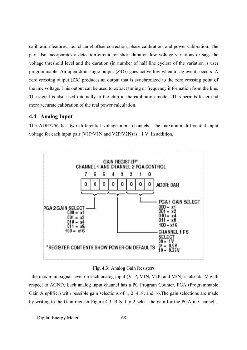
Digital Energy Meter 68
calibration features, i.e., channel offset correction, phase calibration, and power calibration. The
part also incorporates a detection circuit for short duration low voltage variations or sags the
voltage threshold level and the duration (in number of half line cycles) of the variation is user
programmable. An open drain logic output (SAG) goes active low when a sag event occurs .A
zero crossing output (ZX) produces an output that is synchronized to the zero crossing point of
the line voltage. This output can be used to extract timing or frequency information from the line.
The signal is also used internally to the chip in the calibration mode. This permits faster and
more accurate calibration of the real power calculation.
4.4 Analog Input
The ADE7756 has two differential voltage input channels. The maximum differential input
voltage for each input pair (V1P/V1N and V2P/V2N) is ±1 V. In addition,
Fig. 4.3: Analog Gain Resisters
the maximum signal level on each analog input (V1P, V1N, V2P, and V2N) is also ±1 V with
respect to AGND. Each analog input channel has a PC Program Counter, PGA (Programmable
Gain Amplifier) with possible gain selections of 1, 2, 4, 8, and 16.The gain selections are made
by writing to the Gain register Figure 4.3. Bits 0 to 2 select the gain for the PGA in Channel 1

Digital Energy Meter 69
and the gain selection for the PGA in Channel 2 is made via bits 5 to 7. Figure 4.4 shows how a
gain selection for Channel 1 is made using the Gain register[26] .Channel 1 also has a full-scale
input range selection for the ADC. The ADC analog input range selection is also made using the
Gain register—shows Figure 4.4. As mentioned previously, the maximum differential input
voltage is±1 V However, by using Bits 3 and 4 in the Gain register, the maximum ADC input
voltage can be set to 1 V, 0.5 V, or 0.25 V. This is achieved by adjusting the ADC reference
Table I
Fig. 4.4: PGA in Channel -1
summarizes the maximum differential input signal level on Channel 1 for the various ADC range
and gain selections. It is also possible to adjust offset errors on Channel 1 and Channel2 by
writing to the Offset Correction Registers (CH1OS andCH2OS respectively). These registers
allow channel offsets in the range ±20 mV to ±60 mV (depending on the gain setting) to be
removed. Note that it is not necessary to perform an offset correction in Energy measurement
application if HPF1 in Channel 1is switched on. Figure 4.5 shows the effect of offsets on the real
power calculation.. Since this dc component is extracted by LPF2 to generate the Active (Real)
Power information, the offsets will have contributed an error to the Active Power calculation
This problem is easily avoided by enabling HPF1 in Channel 1. By removing the offset from at
least one channel, no error component can be generated at dc by the multiplication. Error terms

Digital Energy Meter 70
at Cos (ωt) are removed by LPF2 and by integration of the Active Power signal in the Active
Energy register (AENERGY[39:0]).
Fig. 4.5: Effects of Channel Offsets on the Real Power Calculation 4.5 Active Power Calculation
Electrical power is defined as the rate of energy flow from source to load. It is given by the
product of the voltage and current waveforms. The resulting waveform is called the
instantaneous power signal and it is equal to the rate of energy flow at every instant of time. The
unit of power is the watt or joules/sec. Equation (3) gives an expression for the instantaneous
power signal in an ac system. The unit of power is the watt or joules/sec.
v(t)= 2 Vsin( t ) (1)
i(t) = 2 Vcos( t ) (2) Where V = rms voltage, I = rms current. p(t)=v(t)×i(t) (3) p(t)= VI- VIcos(2 t )

Digital Energy Meter 71
P=nT
1nT
dttp0
)( =VI (4)
Where T is the line cycle period and P is referred to as the Active or Real power. One note that
the active power is equal to the dc component of the instantaneous power signal p(t) in Equation
3 , i.e., VI. This is the relationship used to calculate active power in the ADE7756.The
instantaneous power signal p (t) is generated by multiplying the current and voltage signals. The
dc componentof the instantaneous power signal is then extracted by LPF2 (Low-Pass Filter) to
obtain the active power information. This process is graphically illustrated in Figure 4.6
Fig. 4.6: Active Power Calculations
Since LPF2 does not have an ideal” brick wall” frequency response may be seen Figure 4.7—the
Active Power signal will have some ripple due to the instantaneous power signal. This ripple is
sinusoidal and has a frequency equal to twice the line frequency. Since the ripple is sinusoidal
immature it will be removed when the Active Power signal is integrated to calculate Energy[26].

Digital Energy Meter 72
Fig. 4.7: Frequency Response of LPF . Active Power Signal Processing Shown in Figure 4.8 is the maximum code (Hexadecimal)
output range for the Active Power signal (LPF2). Note that the output range changes, depending
on the contents of the Active Power Gain register Channel 1 ADC section. The minimum output
range is given when the Active Power Gain register contents are equal to 800h, and the
maximum range is given by writing 7FFh to the Active Power Gain register. This can be used to
calibrate the Active Power (or Energy) calculation in the ADE7756
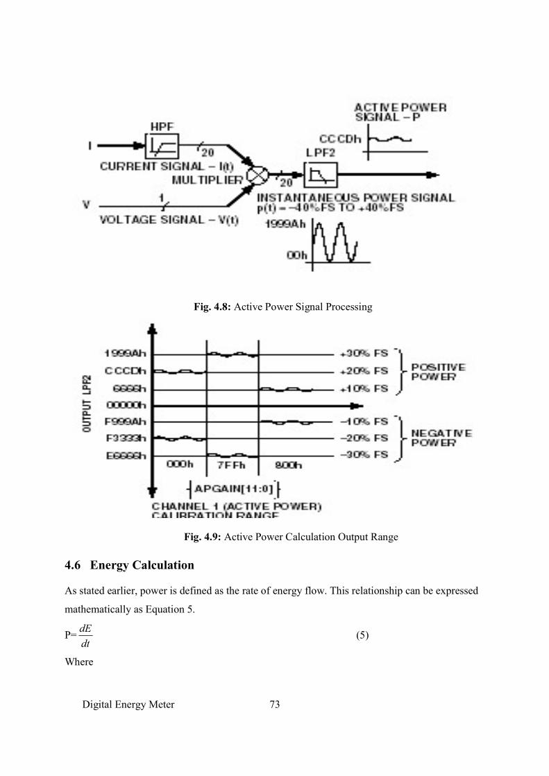
Digital Energy Meter 73
Fig. 4.8: Active Power Signal Processing
Fig. 4.9: Active Power Calculation Output Range 4.6 Energy Calculation As stated earlier, power is defined as the rate of energy flow. This relationship can be expressed
mathematically as Equation 5.
P=dt
dE (5)
Where

Digital Energy Meter 74
P = Power, and E = Energy
Conversely, Energy is given as the integral of Power.
.
E= pdt (6)
The ADE7756 achieves the integration of the Active Power signally continuously accumulating
the Active Power signal in the 40-bitActive Energy register (AENERGY [39:0]). This discrete
time accumulation or summation is equivalent to integration in continuous time. Equation 7
expresses the relationship
E= pdt =Limit { TnTpn
0)( } (7)
T 0 Where n is the discrete time sample number And T is the sample period.
Fig.4.10: Energy Calculations
The discrete time sample period (T) for the accumulation registering the ADE7756 is 1.1 μs
(4/CLKIN). As well as calculating the Energy, this integration removes any sinusoidal
components that may be in the Active Power signal. Figure 4.10 shows a graphical
representation of this discrete time integration or accumulation. The Active Power signal in the
Waveform register is continuously added to the Active Energy register. This addition is a signed
addition; therefore negative energy will be subtracted from the Active Energy contents[26].

Digital Energy Meter 75
4.7 Energy Calibration
By using the on-chip zero-crossing detection on Channel 2 the energy calibration can be greatly
simplified and the time required to calibrate the meter can be significantly reduced. To use the
zero-cross detection the ADE7756 is placed in calibration modeby setting Bit 7 (CMODE) in the
Mode register. In Calibration Mode the ADE7756 accumulates the Active Power signal in the
Active Energy register for an integral number of half cycles, as shown in Figure 4.11.
Fig. 4.11: Energy Calculations in Calibration Mode
The number of half-line cycles is specified in the SAGCYC register. The ADE7756 can
accumulate Active Power for up to 255 half-cycles. Because the Active Power is integrated on an
integral number of line cycles, the sinusoidal component is reduced to zero. This eliminates any
ripple in the energy calculation. Energy is calculated more accurately and in a shorter time
because integration period can be shortened. At the end of an energy calibration cycle the SAG
flag in the Interrupt Status register is set; this will cause the SAG output to go active low. If the
SAG enable bit in the Interrupt Enable register is enabled, the IRQ output will also go active low.
Thus the IRQ line can be used to signal the end of a calibration also. Another calibration cycle
will start as long as the CMODE bit in the Mode register is set. Note that the result of the first

Digital Energy Meter 76
calibration is invalid and must be ignored. The result of all subsequent calibration cycles is
correct[23].From Equations (5 )and other relevant equation,
E(t)= nT
VIdt0
{ Hzfl
VI
9.8/21}
nT
dtt0
)2cos( (8)
Where n is an integer and T is the line cycle period. Since the sinusoidal component is integrated over an integer number of line cycles, its value is always zero. Therefore:
E (t) = nT
VIdt0
(9)
E (t) =VInT (10)
4.8 Analog to Digital Conversion The analog-to-digital conversion in the ADE7756is carried out using two second-order sigma-
delta ADCs. The block diagram in Figure 4.12 shows a first-order (for simplicity) sigma-delta
ADC. . The converter is made up of two parts, first the sigma delta modulator and seconds the
digital low pass filter. A sigma-delta modulator converts the input signal into a continuous serial
streamof1sand 0s at a rate determined by the sampling clock.
Fig.4.12: First Order Sigma Delta ADC
In theADE7756 the sampling clock is equaltoCLKIN/4. The 1-bit DAC in the feedback loop is
driven by the serial. Sampling interval, the data from the 1-bit ADC is virtually meaningless.

Digital Energy Meter 77
Only when a large number of samples are averaged, will a meaningful result be obtained.This
averaging is carried out in the second part of the ADC, the digital low-pass filter. By averaging
large number of bits from the modulator the low-pass filter can produce 20-bit data words that
are proportional to the Input signal level .The sigma-delta converter uses two techniques to
achieve high-resolution from what is essentially a 1-bit conversion technique. The first is over
sampling By over sampling we mean that the signal is sampled at a rate (frequency) that is many
times higher than the bandwidth of interest..
Fig. 4.13: Noise Reduction Due to over sampling and Noise Shaping in the Analog Modulator
For example, the sampling rate in the ADE7756 is CLKIN/4 (894 kHz) and the band of interest
is 40 Hz to 2 kHz. Over sampling has the effect of spreading the quantization noise (noise due to
sampling) over a wider bandwidth. With the noise spread more thinly over a wider bandwidth,

Digital Energy Meter 78
the quantization noise in the band of interest is lowered—shows Figure 4.15 However over
sampling alone is not an efficient enough method to improve the signal to noise ratio (SNR) in
the band of interest. For example, an over sampling ratio of 4 is required just to increase the SNR
by only 6 dB(1 bit). To keep the over sampling ratio at a reasonable level, it is possible to shape
the quantization noise so that the majority of the noise lies at the higher frequencies. This is what
happens in the sigma-delta modulator, the noise is shaped by the integrator which has a high-
pass-type response for the quantization noise. The result is that most of the noise is at the higher
frequencies where it can be removed by the digital low-pass filter. This noise shaping is also
shown in Figure 4.13 [27].
4.9 Calibrating the Energy Meter
4.9.1 Calculating the Average Active Power
When calibrating the ADE7756, the first step is to calibrate the frequency on CF to some
required meter constant, e.g.,3200 imp/kW H .In order to determine the output frequency on CF,
the average value of the Active Power signal (output of LPF2) must first be determined. One
convenient way to do this is to use the calibration mode. When the CMODE (Bit 7) bit in the
Mode register is set to a Logic 1, energy is accumulated over an integer number of half-line
cycles. Since the line frequency is fixed at, assume, 50Hz, and the number of half-cycles of
integration is specified, the total integration time is given as:[26]
Hz502
1Number of half cycle
For 255 half-cycles this would give a total integration time of2.125 seconds. This would mean the energy register is updated2.125/1.1175 μs (4/CLKIN) times. The average output value of LPF2 is given as: Or equivalently, in terms of contents of various ADE7756AN registers and CLKIN and line frequencies (fl):
Average word (LPF2) =CLKINSAGCYC
flAENERGY
]0:7[
8]0:39[
Where fl is the line frequency
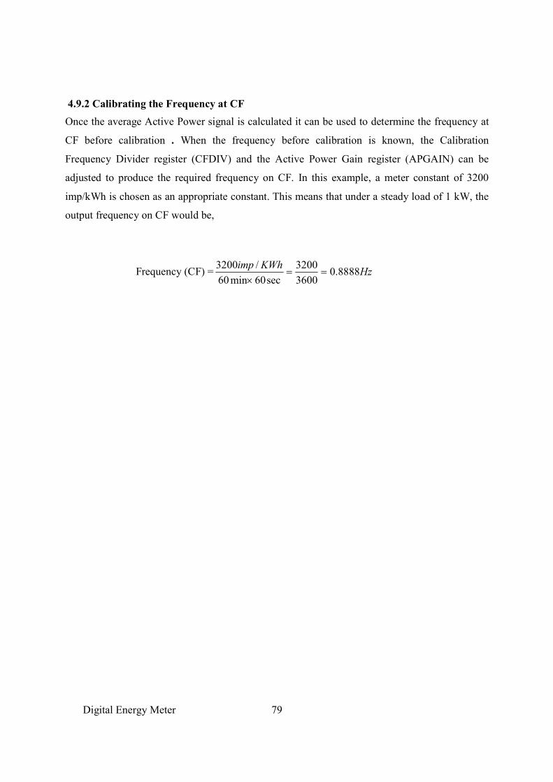
Digital Energy Meter 79
4.9.2 Calibrating the Frequency at CF
Once the average Active Power signal is calculated it can be used to determine the frequency at
CF before calibration . When the frequency before calibration is known, the Calibration
Frequency Divider register (CFDIV) and the Active Power Gain register (APGAIN) can be
adjusted to produce the required frequency on CF. In this example, a meter constant of 3200
imp/kWh is chosen as an appropriate constant. This means that under a steady load of 1 kW, the
output frequency on CF would be,
Frequency (CF) = HzKWhimp
8888.03600
3200
sec60min60
/3200

80
CHAPTER-5
DESIGN AND DEVELOPMENT OF MICROCONTROLLER BASED ENERGY METER SYSTEM
5.1 Introduction
The goal of the thesis is generation, transmission and reception of digital energy meter reading from
consumer residence to organization using SMS technology under coverage by GSM network. For this
purpose initially design the circuit, write appropriate program, install program into microcontroller and
assemble all the equipments have been done in a test board for easier testing and modifying. When it is
worked successfully then transfers to the main circuit board. It may be noted that write program in Basic
and Assemble programming language and PIC BASIC Pro software uses as compiler. The program code
saves as text file and run through compiler. The compiler reads the text file and generates an equivalent
machine code instruction list of the program. The list of instruction is a hexadecimal file that represents
PICBASIC Pro Program. The program is uploaded into PIC18F2550 microcontroller using programmer
and EPIC Win software.
5.2 Block Diagram and Descriptions of Each Block
The overall block diagram of the system is shown in figure:5 1 The system mainly consists of energy
measuring chip, microcontroller, GSM- module including SIM and liquid crystal display. The functions
of each block are gradually given below.
Energy Measuring Chip: The energy measuring chip of digital energy meter consists of
comparators circuit, analog to digital converter (ADCs), low pass filter, high pass filter,
multiplier, phase adjuster, wave and real power resister. The comparators circuit senses the
voltage and current indirectly in analog signal mode and converts the analog signal into
digital signal using the analog to digital converters. The digital value of voltage, current and
power factor are multiplied by multiplier circuit and produce the real power. This real power
holds by the wave register for few seconds and later provide to the real power register in
binary form. It may be noted that high pass filter and low pass filter are used for filtering the
unwanted frequency.
Microcontroller: The microcontroller is a small computer that composed of program
memory, data memory, data EEPROM, program counter(PC), instruction register(IR), data
bus, address bus, oscillators, timers, ALU and I/O ports etc. In this system program is
loaded into program memory and data memory is used for keeping the data on temporary
basic. The data memory controls the peripheral functions also. As per program the
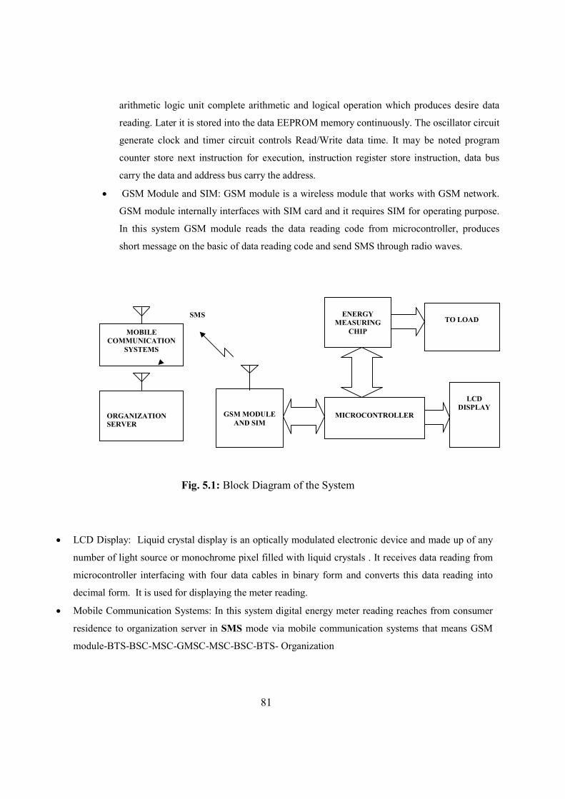
81
arithmetic logic unit complete arithmetic and logical operation which produces desire data
reading. Later it is stored into the data EEPROM memory continuously. The oscillator circuit
generate clock and timer circuit controls Read/Write data time. It may be noted program
counter store next instruction for execution, instruction register store instruction, data bus
carry the data and address bus carry the address.
GSM Module and SIM: GSM module is a wireless module that works with GSM network.
GSM module internally interfaces with SIM card and it requires SIM for operating purpose.
In this system GSM module reads the data reading code from microcontroller, produces
short message on the basic of data reading code and send SMS through radio waves.
a
.
5.3 Work Flow Diagram of the System The work flow diagram of the system is shown in figure 5.2
GSM MODULE AND SIM
MICROCONTROLLER
ORGANIZATION SERVER
LCD
DISPLAY
ENERGY
MEASURING CHIP
TO LOAD
SMS
MOBILE COMMUNICATION
SYSTEMS
LCD Display: Liquid crystal display is an optically modulated electronic device and made up of any
number of light source or monochrome pixel filled with liquid crystals . It receives data reading from
microcontroller interfacing with four data cables in binary form and converts this data reading into
decimal form. It is used for displaying the meter reading.
Mobile Communication Systems: In this system digital energy meter reading reaches from consumer
residence to organization server in SMS mode via mobile communication systems that means GSM
module-BTS-BSC-MSC-GMSC-MSC-BSC-BTS- Organization
81
Fig. 5.1: Block Diagram of the System
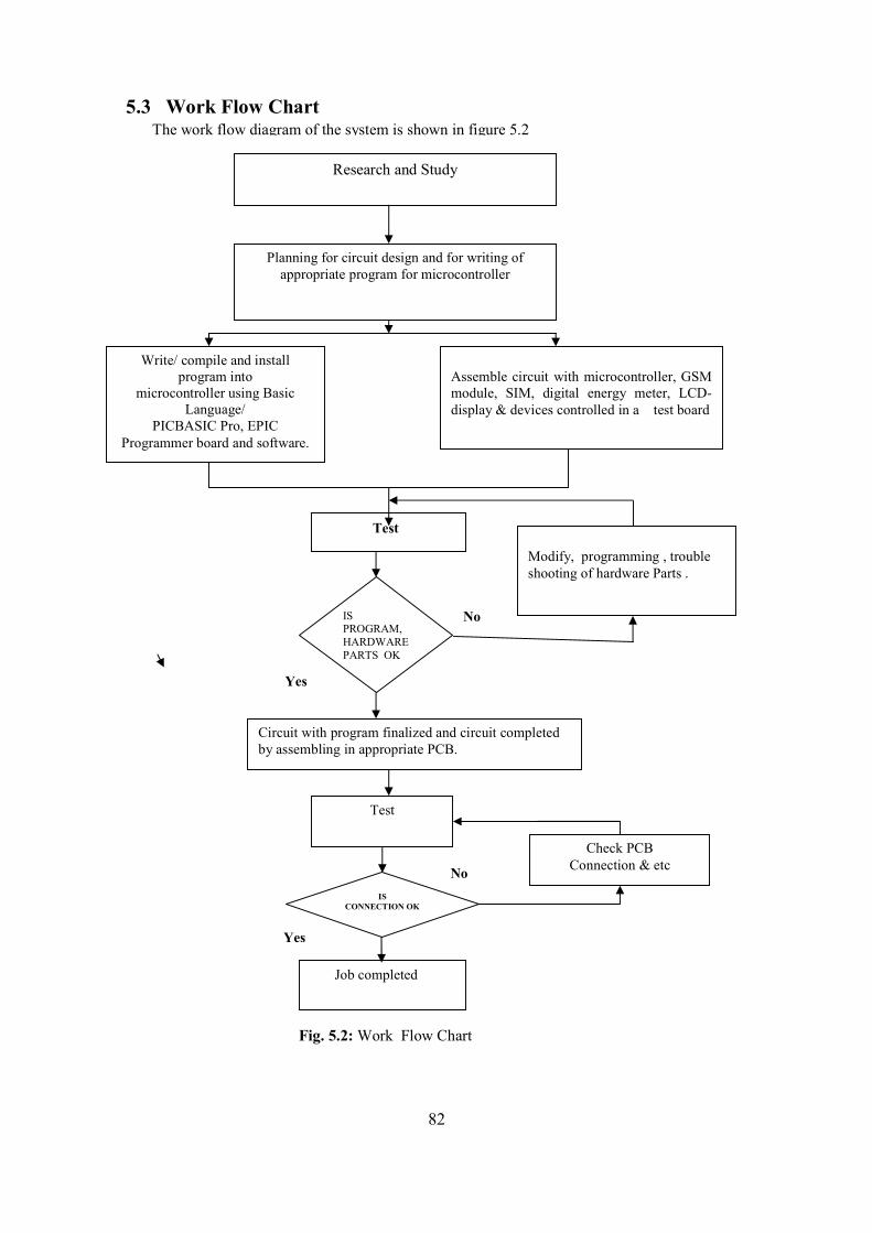
82
Research and Study
Planning for circuit design and for writing of appropriate program for microcontroller
Write/ compile and install program into
microcontroller using Basic Language/
PICBASIC Pro, EPIC Programmer board and software.
Assemble circuit with microcontroller, GSM module, SIM, digital energy meter, LCD-display & devices controlled in a test board
Test Modify, programming , trouble shooting of hardware Parts .
IS PROGRAM, HARDWARE PARTS OK
Circuit with program finalized and circuit completed by assembling in appropriate PCB.
Yes
Test
IS CONNECTION OK
Job completed
Check PCB Connection & etc
No
Yes
No
Fig. 5.2: Work Flow Chart
5.3 Work Flow Chart The work flow diagram of the system is shown in figure 5.2

83
5.4 Program Flow Chart of the System
The program flow chart of the system is shown in figure 5.3
START
DEFINE LCD IN/OUT PIN
DEFINE PHONE NUMBER
READ EEPROM
SETTING DATE
COUNTING DATE
IS SETTING DATE
=COUNTING DATE
READ DIGITAL ENERGY METER READING
CALCULATE READING IN KWH FORM
DISPLAY READING ON LCD EACH 10 SECOND
WRITE EEPROM
No
Yes
ENABLE GSM MODULE
SEND AND DELETE MESSAGE
Fig. 5.3: Program Flow Chart of the System
CONNECT GSM
MAIN PROGRAM
IS POWER AVAILABL
WRITE DATA EEPROM
GOTO MAIN PROGRAM
YES No

84
5.5 Interfacing Circuit When one circuit or module interfaces with another circuit or module by some components then it is
called interfacing circuit.
5.5.1 Interfacing Circuits between Microcontroller and GSM Module
The figure 5.4(a), 5.4(b) 5.4(c) and represents the interfacing circuit between MCU and GSM module that are used for different activities.
The 5.4(b) interfacing circuit is used for maintaining the time continuation that means GSM
Fig. 5.4 (a): Interfacing Circuit between GSM Module and Microcontroller
The 5.4(a) interfacing circuit is used for providing the digital energy meter reading from microcontroller to the GSM module at the first day of the each month. By this circuit MCU always send request signal to the GSM module for knowing time from GSM network. In this circuit Zener diode is used for providing the constant voltage supply to the GSM Module from MCU. When the value of the voltage is going to be above 3.9V in that case excess voltage will be drop across the resistor 220R and maintain to provide the constant voltage supply to the GSM module. The GSM Module takes time from GSM network and provide this time to the microcontroller. By this circuit GSM module gives reply about time to microcontroller corresponding each request signal each second later. In this circuit two transistors are used for switching purpose. The working mechanism of this circuit such as when active low voltage signal is applied to the first transistor base in that case transistor will go to cut off reason and output of the first transistor will be active high. This high voltage signal will be applied to the base of the second transistor. In that case the second transistor will go to the saturation reason and output of it will be low and that is applied to the MCU.
The 5.4(a) interfacing circuit is used for providing the digital energy meter reading from microcontroller to the GSM module at the first day of the each month. By this circuit MCU always send request signal to the GSM module for knowing time from GSM network. In this circuit Zener diode is used for providing the constant voltage supply to the GSM Module from MCU. When the value of the voltage is going to be above 3.9V in that case excess voltage will be drop across the resistor 220R and maintain to provide the constant voltage supply to the GSM module.

85
Whereas when the high voltage signal is applied to the first transistor base in that case the transistor will
go to saturation reason and output will be low. This low voltage signal is applied to the base of the
second transistor and in that case output will be high that is applied to the microcontroller terminal.
Fig. 5.4 (b): Interfacing Circuit between GSM Module and Microcontroller
Fig.5.4(c): Interfacing Circuit between GSM Module and Microcontroller

86
5.5.2 Interfacing Circuit between GSM Module and GSM Network
Fig. 5.5: Interfacing Circuit between GSM Module and GSM Network.
This is the interfacing between GSM networks and GSM module. By this circuit GSM module
takes information about network .The first blinking of LED indicates that the network is not
available and whereas the slow blinking of LED indicate that the network is available.
5.5.3 Interfacing Circuit Between Microcontroller and Energy Measuring Chip
This is the interfacing circuit between microcontroller and energy measuring chip .The energy measuring
chip terminal 17(CS), 18(Dout), 19(Sclk) and 20(Din) directly interfaced with microcontroller pin
14(VUSB), 13(RC2/CCP1), 12(RC1/TIOS1) and 11(RCO/TIOSO). The four line is made communication
between EMC and MCU. The CS means chip select pin part of the 4-wire serial interface. This active low
logic input allows the ADE7756 to share the serial bus with several other devices. The SCLK means
serial clock input for the synchronous serial interface. All serial data transfers are synchronized to this
clock. The SCLK has a Schmitt-trigger input for use with a clock source that has a slow edge transition
time, e.g., opto-isolator outputs. The DOUT means data output for the serial interface. Data is shifted out
at this pin on the rising edge of SCLK. The DIN means data input for the serial interface. Data is shifted
in at this pin on the falling edge of SCLK
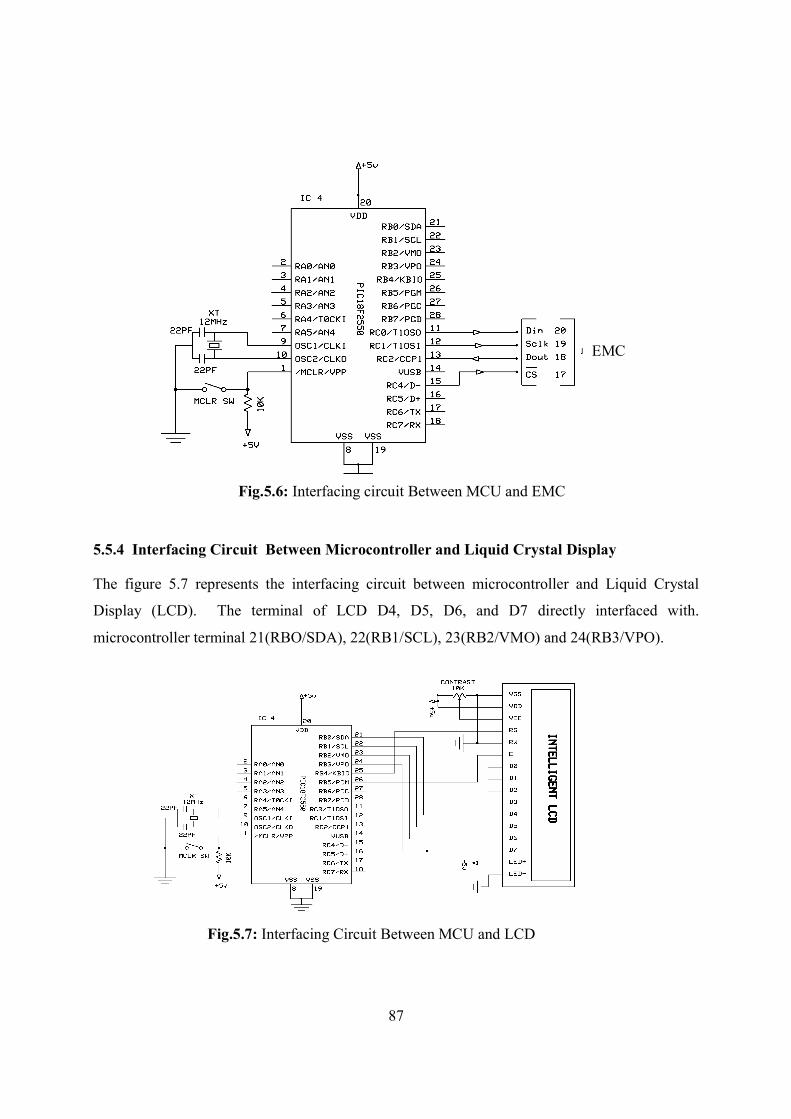
87
5.5.4 Interfacing Circuit Between Microcontroller and Liquid Crystal Display
The figure 5.7 represents the interfacing circuit between microcontroller and Liquid Crystal
Display (LCD). The terminal of LCD D4, D5, D6, and D7 directly interfaced with.
microcontroller terminal 21(RBO/SDA), 22(RB1/SCL), 23(RB2/VMO) and 24(RB3/VPO).
EMC
Fig.5.6: Interfacing circuit Between MCU and EMC
Fig.5.7: Interfacing Circuit Between MCU and LCD

88
The enable and reset terminal E and RS of LCD display directly interfaced with microcontroller
terminal 25(RB4/KB10) and 26(RB5/PGM) respectively. This circuit is used for providing the
digital energy meter reading from MCU to LCD display.
5.5.5 Interfacing Circuit Between GSM Module and SIM
The figure 5.8 represents the interfacing circuit between module and SIM. The module power
pin (SIM_VDD) directly connected with SIM power pin VDD. The module reset pin RST_SIM
connected with SIM pin SIM_RST through 22R. Either used itself (reset signal supplied from the
interface device) or in combination with an internal reset control circuit (optional use by the card) The
module clock pin SIM_CLK connected with SIM clock pin SIM_CLK via 22R. CLOCK: Clocking or
timing signal (optional use by the card) provide from module. Again the module data pin (SIM_DATA)
interfaced with SIM pin SIM _DATA via 22R . GND: Ground (reference voltage). DATA: Input or
Output for serial data to the integrated circuit inside the card.
5.6 Power Supply Unit
Power supply is a reference to a source of electrical power. A device or system that supplies electrical or
other types of energy to an output load or group of loads is called a power supply unit or PSU. The term is
most commonly applied to electrical energy supplies, less often to mechanical ones, and rarely to others
Fig. 5.8 : Interfacing Circuit Between GSM Module and SIM
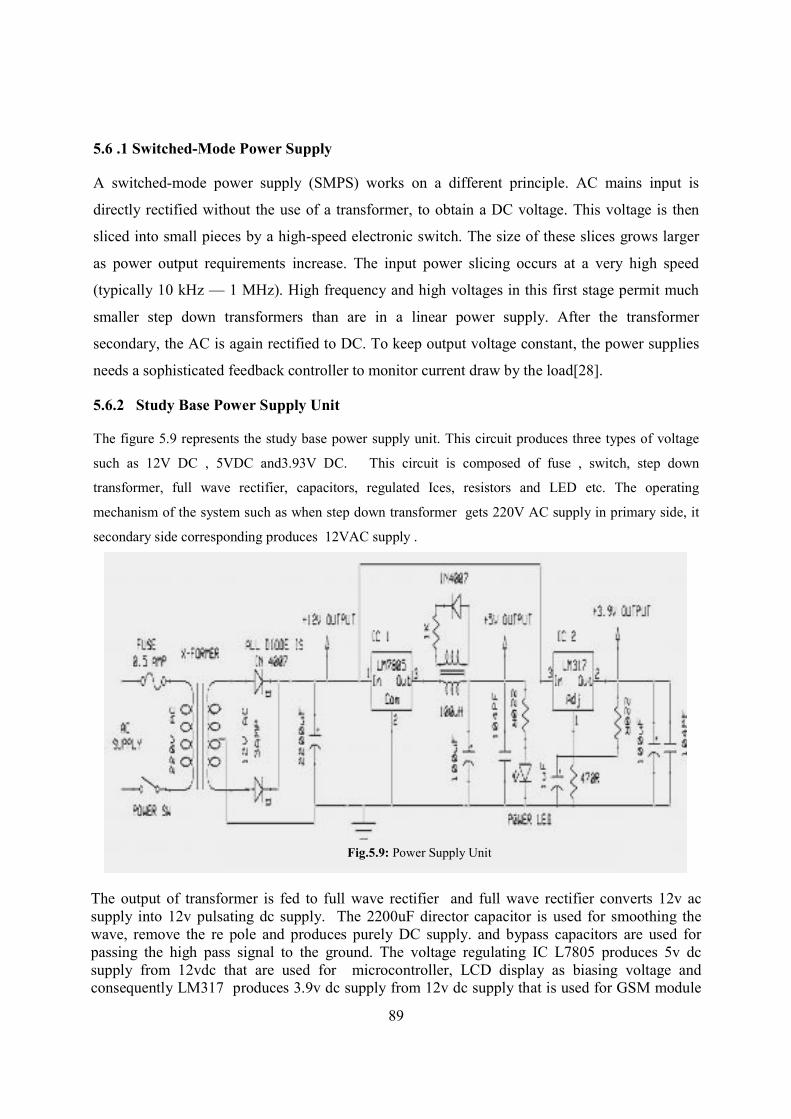
89
5.6 .1 Switched-Mode Power Supply
A switched-mode power supply (SMPS) works on a different principle. AC mains input is
directly rectified without the use of a transformer, to obtain a DC voltage. This voltage is then
sliced into small pieces by a high-speed electronic switch. The size of these slices grows larger
as power output requirements increase. The input power slicing occurs at a very high speed
(typically 10 kHz — 1 MHz). High frequency and high voltages in this first stage permit much
smaller step down transformers than are in a linear power supply. After the transformer
secondary, the AC is again rectified to DC. To keep output voltage constant, the power supplies
needs a sophisticated feedback controller to monitor current draw by the load[28].
5.6.2 Study Base Power Supply Unit
The figure 5.9 represents the study base power supply unit. This circuit produces three types of voltage
such as 12V DC , 5VDC and3.93V DC. This circuit is composed of fuse , switch, step down
transformer, full wave rectifier, capacitors, regulated Ices, resistors and LED etc. The operating
mechanism of the system such as when step down transformer gets 220V AC supply in primary side, it
secondary side corresponding produces 12VAC supply .
Fig.5.9: Power Supply Unit
The output of transformer is fed to full wave rectifier and full wave rectifier converts 12v ac supply into 12v pulsating dc supply. The 2200uF director capacitor is used for smoothing the wave, remove the re pole and produces purely DC supply. and bypass capacitors are used for passing the high pass signal to the ground. The voltage regulating IC L7805 produces 5v dc supply from 12vdc that are used for microcontroller, LCD display as biasing voltage and consequently LM317 produces 3.9v dc supply from 12v dc supply that is used for GSM module

90
5.7 Feature of Study Based Microcontroller ( PIC18F2550 )
The feature of PIC18F2550 microcontroller is shown in table 5.1.
Table. 5.1 Feature of Study Base Microcontroller
Features PIC18F2550
Operating Frequency DC – 48 MHz
Program Memory (Bytes)
32768
Program Memory (Instructions)
16384
Data Memory (Bytes)
2048
Data EEPROM Memory (Bytes)
256
Interrupt Sources 19 I/O Ports Ports A, B, C, (E) Timers 4 Capture/Compare/PWM Modules 2 Enhanced Capture/ Compare/PWM Modules
0
Serial Communications
MSSP, Enhanced USART
pin SOIC Universal Serial Bus (USB) 1 Streaming Parallel Port (SPP) No 10-Bit Analog-to-Digital Module 10 Input Channels Comparators 2 Resets (and Delays)
POR, BOR, RESET Instruction,
Stack Full, Stack Underflow (PWRT, OST),
MCLR (optional), WDT
Programmable Low-Voltage Detect
Yes
Programmable Brown-out Reset Yes
Packages
28-pin PDIP 28-pin SOIC

Design & Development 91
5.8 GSM Module
GSM Modules are similar to GSM Modems, but there's one difference: A GSM Modem is an
external equipment, whereas the GSM Module is a module that can be included within an
equipment. It is an embedded piece of hardware. A GSM module is a wireless module that works
with GSM networks. A wireless module behaves like a Hayes compatible dial-up modem. The
main difference between a standard Hayes modem and a GSM module is that a Hayes modem
sends and receives data through a fixed telephone line while a GSM module sends and receives
data through radio waves. Like a GSM mobile phone, a GSM module requires a SIM card from a
wireless carrier in order to operate. GSM modules and normal Hayes modems support a common
set of AT commands. A GSM module can be used just like a Hayes compatible modem. GSM
modules support an extended set of AT commands. These extended AT commands are defined in
the GSM standards. With the extended AT commands, we can do things like:
Read, write and delete SMS messages.
Send SMS messages.
Monitor the signal strength.
Monitor the charging status and charge level of the battery.
Read, write and search phone book entries.
The number of SMS messages that can be processed by a GSM module is pretty low, approx six
messages per minute. GPRS Modules are similar to modems, but there's one difference: A GRPS
Modem is external equipment, whereas the GPRS Module is a module that can be integrated
within equipment. It is an embedded piece of hardware A GPRS module is a GSM module with
additional support for GPRS technology for data transmission. GPRS means: General Packet
Radio Service'. It is based on a packet-switched technology, as an extension to GSM (note that
GSM is a circuit-switched). An advantage of GPRS over GSM is that GPRS has transmission
speed. a much higher data GPRS can be used as the bearer of SMS. If SMS over GPRS is used,
an SMS transmission speed of about 30 SMS messages per minute may be achieved. This is
much faster than SMS over GSM. A GPRS modem is required to send and receive SMS via
GPRS. Some wireless carriers do not support the sending and receiving of SMS via GPRS. In
this study SIM 300 module is used.

Design & Development 92
5.8.1 Pin Diagram of Study Base GSM Module (SIM300CZ)
The pin diagram of study base module is shown in figure 5.10
Fig.5.10: Pin Diagram of GSM Module

Design & Development 93
5.8.2 Features of GSM Module SIM 300CZ
SIM300 is a Tri-band GSM/GPRS module that works on frequencies EGSM 900 MHz, DCS 1800 MHz
and PCS 1900 MHz. SIM300 features GPRS multi-slot class 10/ class 8 (optional) and supports the GPRS
coding schemes CS-1, CS-2, CS-3 and CS-4. With a small configuration of 40mm x 33mm x 2.85mm,
SIM300 can fit almost all the space requirements in the applications, such as smart phone, PDA phone
and other mobile devices. The physical interface to the mobile application is made through a 60-pin
board-to-board connector, which provides all hardware interfaces between the module and customers’
boards except the RF antenna interface.
The keypad and SPI display interface will give you the flexibility to develop customized
applications.
Serial port and Debug port can help us easily develop our applications.
Two audio channels include two microphones inputs and two speaker outputs. This can be easily
configured by AT command.
The SIM300 provides RF antenna interface with two alternatives: antenna connector and antenna pad.
The antenna connector is MURATA MM9329-2700. And customer’s antenna can be soldered to the
antenna pad. The SIM300 is designed with power saving technique; the current consumption is as low as
2.5mA in SLEEP mode. The SIM300 is integrated with the TCP/IP protocol; extended TCP/IP AT
commands are developed for customers to use the TCP/IP protocol easily, which is very useful for those
data transfer applications[29].
Table 5.2 Feature of GSM Module
Feature Implementation
Power supply Single supply voltage 3.4V – 4.5V
Power saving
Typical power consumption in SLEEP mode to 2.5mA ( BS-PA-
MFRMS=5 )
Frequency bands
SIM300 Tri-band: EGSM 900, DCS 1800, PCS 1900. The SIM300 can search the 3 frequency bands automatically. The frequency bands also can be set by AT command.
Compliant to GSM Phase 2/2+
GSM class Small MS
Transmit power Class 4 (2W) at EGSM 900 Class 1 (1W) at DCS 1800 and PCS 1900

Design & Development 94
Feature Implementation
GPRS connectivity
GPRS multi-slot class 10 (default)
GPRS multi-slot class 8 (option) GPRS mobile station class B
DATA GPRS: CSD:
GPRS data downlink transfer: max. 85.6 kbps GPRS data uplink transfer: max. 42.8 kbps Coding scheme: CS-1, CS-2, CS-3 and CS-4 SIM300 supports the protocols PAP (Password
Authentication Protocol) usually used for PPP connections. The SIM300 integrates the TCP/IP protocol. Support Packet Switched Broadcast Control Channel
(PBCCH) CSD transmission rates: 2.4, 4.8, 9.6, 14.4 kbps, non-
transparent Unstructured Supplementary Services Data (USSD) support
SMS
MT, MO, CB, Text and PDU mode SMS storage: SIM card
FAX
Group 3 Class 1
SIM interface
Support SIM card: 1.8V, 3V
External antenna
Connected via 50 Ohm antenna connector or antenna pad
Audio features
Speech codec modes: Half Rate (ETS 06.20) Full Rate (ETS 06.10) Enhanced Full Rate (ETS 06.50 / 06.60 / 06.80) Echo suppression
Physical characteristics
Size: 40±0.15 x 33±0.15 x 3.3±0.3mm (including application connector)
40±0.15 x 33±0.15 x 2.85±0.3mm (excluding application connector)
Weight: 8g
Real time clock(RTC)
Implemented
Firmware upgrade
Firmware upgrade by serial port.

Design & Development 95
5.8.3 Functional Diagram of GSM Module SIM 300CZ
The following figure 5.11 shows a functional diagram of the SIM 300CZ and illustrates the mainly
functional part:
Fig. 5.11 : Functional Diagram of GSM Module SIM 300CZ
The GSM base band engine
Flash and SRAM
The GSM radio frequency part
The antenna interface
The board-to-board interface

Design & Development 96
5.8 .4 Top view of GSM Module SIM 300CZ The top view of GSM Module is shown in figure 5.12
Fig. 5.12: Top view of GSM Module SIM300CZ 5.8.5 Bottom view of GSM Module SIM 300CZ The bottom view of GSM module is shown in figure5.13
Fig. 5.13: Bottom view of GSM Module SIM300 CZ

Design & Development 97
5.8.6 Operating Modes of GSM Module SIM 300CZ The table below briefly summarizes the various operating modes [29]. Table 5 .3 Various Operation Mode of GSM Module
Mode Function Normal operation GSM/GPRS SLEEP Module will automatically go into SLEEP mode if DTR
is set to high level and there is no on air and no hardware interrupt (such as GPIO interrupt or data on serial port). In this case, the current consumption of module will reduce to the minimal level. During SLEEP mode, the module can still receive paging message and SMS from the system normally.
GSM IDLE Software is active. Module has registered to the GSM network, and the module is ready to send and receive.
GPRS STANDBY Module is ready for GPRS data transfer, but no data is currently sent or received. In this case, power consumption depends on network settings and GPRS configuration.
GPRS DATA There is GPRS data in transfer (PPP or TCP or UDP). In this case, power consumption is related with network settings (e.g. power control level), uplink / downlink data rates and GPRS configuration (e.g. used multi-slot settings).
5.8. 7 Pin Descriptions of GSM Module
The SIM interface supports the functionality of the GSM Phase 1 specification and also supports the
functionality of the new GSM Phase 2+ specification for FAST 64 kbps SIM. The SIM interface is
powered from an internal regulator in the module having normal voltage 3V. All pins reset as outputs
driving low[26]. Logic levels are as described in below table
Table 5.4 Pin Functions of GSM Module
Name
Pin(GSM
Module)
Function
SIM_VDD 25 SIM Card Power output automatic output on SIM mode one is 3.0V±10%, another is 1.8V±10%. Current is about 10mA.
SIM_DATA 29 SIM Card data I/O
SIM_CLK 31 SIM Card Clock
SIM_RST 27 SIM Card Reset

Design & Development 98
5.9 Pin Description of the SIM Card
Table 5.5 Pin Functions of SIM Card
Name Description
VDD +3 V DC power supply input from module(optional use by the card).
RESET
Either used itself (reset signal supplied from the interface device) or in combination with an
internal reset control circuit (optional use by the card). If internal reset is implemented, the
voltage supply on Vcc is mandatory
CLOCK Clocking or timing signal (optional use by the card)
GND Ground (reference voltage)
DATA Input or Output for serial data to the integrated circuit inside the card
5.10 SIM Card Holder
For 6 pins SIM card, usually Amphenol C707 10M006 SIM Card holders are used. The diagram of the
SIM card holder is shown in figure 5.14
Fig.5.14: Diagram of the SIM Card Holder

Design & Development 99
The dialogue between the interface device and the card shall be conducted through the consecutive
operations:
connection and activation of the contacts by the interface device
reset of the card
answer to reset by the card
subsequent information exchange between the card and the interface device
deactivation of the contacts by the interface device
The adapter electronic gets its power supply from the smartcard reader device VCC line or an external 5
V supply can be used [30]. The card slot’s RST line is connected using one of the TTL->RS-232 drivers
in the MAX232 to DCD, so that the software and the reader can easily resynchronize in case of a protocol
error
5.11 Liquid Crystal Display
A liquid crystal display (LCD) is an electronically-modulated optical device shaped into a thin, flat panel
made up of any number of color or monochrome pixels filled with liquid crystals and arrayed in front of a
light source (backlight) or reflector. It is often utilized in battery-powered electronic devices because it
uses very small amounts of electric power. The nematic phase is characterized by the orientational order
of the constituent molecules. The molecular orientation (and hence the material's optical properties) can
be controlled with applied electric fields. Nematics are (still) the most commonly used phase in liquid
crystal displays (LCDs), with many such devices using the twisted nematic geometry.
Fig: 5.15 : Reflective twisted nematic liquid crystal display
Reflective twisted nematic liquid crystal display [31].
1. Polarizing filter film with a vertical axis to polarize light as it enters.

Design & Development 100
2. Glass substrate with ITO electrodes. The shapes of these electrodes will determine the shapes that
will appear when the LCD is turned ON. Vertical ridges etched on the surface are smooth.
3. Twisted nematic liquid crystal.
4. Glass substrate with common electrode film (ITO) with horizontal ridges to line up with the
horizontal filter.
5. Polarizing filter film with a horizontal axis to block/pass light.
6. Reflective surface to send light back to viewer. (In a backlit LCD, this layer is replaced with a
light source.)
5.12 Outline of LCD Module
Each pixel of a LCD typically consists of a layer of molecules aligned between two transparent
electrodes, and two polarizing filters, the axes of transmission of which are (in most of the cases)
perpendicular to each other. With no actual liquid crystal between the polarizing filters, light passing
through the first filter would be blocked by the second (crossed) polarizer .The surfaces of the electrodes
that are in contact with the liquid crystal material are treated so as to align the liquid crystal molecules in
a particular direction. This treatment typically consists of a thin polymer layer that is unidirectional
rubbed using, for example, a cloth. The direction of the liquid crystal alignment is then defined by the
direction of rubbing. Electrodes are made of a transparent conductor called Indium Tin Oxide
(ITO).Before applying an electric field, the orientation of the liquid crystal molecules is determined by
the alignment at the surfaces. In a twisted nematic device (still the most common liquid crystal device),
the surface alignment directions at the two electrodes are perpendicular to each other, and so the
molecules arrange themselves in a helical structure, or twist. This reduces the rotation of the polarization
of the incident light, and the device appears grey. If the applied voltage is large enough, the liquid crystal
molecules in the center of the layer are almost completely untwisted and the polarization of the incident
light is not rotated as it passes through the liquid crystal layer. This light will then be mainly polarized
perpendicular to the second filter, and thus be blocked and the pixel will appear black. By controlling the
voltage applied across the liquid crystal layer in each pixel, light can be allowed to pass through in
varying amounts thus constituting different levels of gray.The optical effect of a twisted emetic device in
the voltage-on state is far less dependent on variations in the device thickness than that in the voltage-off
state. Because of this, these devices are usually operated between crossed polarizer such that they appear
bright with no voltage (the eye is much more sensitive to variations in the dark state than the bright state).
These devices can also be operated between parallel polarizer, in which case the bright and dark states are
reversed. The voltage-off dark state in this configuration appears blotchy, however, because of small
variations of thickness across the device .Both the liquid crystal material and the alignment layer material

Design & Development 101
contain ionic compounds. If an electric field of one particular polarity is applied for a long period of time,
this ionic material is attracted to the surfaces and degrades the device performance. This is avoided either
by applying an alternating current or by reversing the polarity of the electric field as the device is
addressed (the response of the liquid crystal layer is identical, regardless of the polarity of the applied
field)[31]. When a large number of pixels are needed in a display, it is not technically possible to drive
each directly since then each pixel would require independent electrodes. Instead, the display is
multiplexed. In a multiplexed display, electrodes on one side of the display are grouped and wired
together (typically in columns), and each group gets its own voltage source. On the other side, the
electrodes are also grouped (typically in rows), with each group getting a voltage sink. The groups are
designed so each pixel has a unique, unshared combination of source and sink. The electronics or the
software driving the electronics then turns on sinks in sequence, and drives sources for the pixels of each
sink.
5.13 PICBASIC and PICBASIC PRO Compilers
PICBASIC is a compiler developed by COMFILE Technology and is programmed in a form of the
BASIC language. The PICBASIC PRO Compiler (or PBP) makes it even quicker and easier to program
Microchip Technology’s powerful PIC microcontrollers (MCUs). The English-like BASIC language is
much easier to read and write than the quirky Microchip assembly language. The PICBASIC and
PICBASIC PRO Compilers both functions in the same way. The program code, saved as a text file is run
through either the PICBASIC or PICBASIC Pro compiler. The compiler reads through the text file and
creates (or compiles) an equivalent machine code instruction listing (the hex file) of the program. The
machine code is a list of hexadecimal numbers that represents the PICBASIC PRO program. The hex file
is uploaded (or programmed) in to the microcontroller. When the microcontroller started its CPU will run
through the programmed list of hexadecimal numbers that run the PICBASIC Pro program. Uploading the
machine code into the microcontroller is the job of the EPIC programmer board and software. The
PICBASIC PRO (Professional) compiler is considerably more expensive than the standard PICBASIC
compiler. The Pro version offers a richer, more enhanced Basic command syntax than is available in the
Picbasic compiler packages. A few of the additional commands that can be found in the Pro version allow
the use of Interrupts, direct control of Liquid crystal display (LCD) modules, dual-tone multi-frequency
(DTMF) out, and X-10 commands, to name a few. PICBASIC PRO (PBP) is compatible with Windows
98/Me/NT/2000/XP/Vista. It supports over 300 of Microchip's PIC microcontrollers, including the very
latest releases. From the tiny, inexpensive 6-pin parts to the immensely powerful 100-pin parts, PBP
allows you to choose the microcontroller that best fits your application. Used by thousands of engineers,
students, and hobbyists for more than a decade, the PICBASIC PRO Compiler is one of the most popular

Design & Development 102
development tools ever created for the PIC microcontroller [32]. A new 32-bit version of PBP (PBPL) is
included that offers BIT, BYTE, WORD, and LONG (32-bit, signed)* variable types. This LONG version
is intended for use with the PIC18 family devices. When working with LONGs, the mathematical
operators return signed results in 32-bit, twos-complement format. This allows storage, calculation, and
display of values from -2,147,483,648 to 2,147,483,647 [33].
5.13.1 Comparison Between PICBASIC and PICBASIC Pro Compilers
Table 5.6 Comparison Between PICBASIC and PICBASIC Pro Compilers
PICBASIC™ Compiler PICBASIC PRO™ Compiler
Limited to first 2K code space. Uses all available code space.
Interrupt handlers must be Assembly
language.
Interrupt handler routines may be either PICBASIC
PRO or Assembly.
Uses Peek and Poke commands to access
internal registers and move contents to and
from pre-defined variables.
Internal register names may be used directly, even in
calculations and conditional statements.
Some built-in commands can only be used on
PortB, PortC or GPIO. While all ports may
be accessed with Peek and Poke, some aren't
available for commands like Serout, Pulsin,
etc.
Software-based commands may be used on any
available port/pin. (Commands that utilize a
hardware module are limited to the pins dedicated to
that module. Some pins have special characteristics
that might cause compatibility issues.)
Clock speed pre-defined at 4MHz. Clock speeds from 3.5975 to 48MHz, depending
upon device capabilities.
Most 14-bit core PICmicro® MCUs
supported.
ALL PICmicro® MCUs are supported, including 12-
bit core, 17CXXX, 18CXXX, and 18FXXX.
5.13.2 Additional commands available only in PICBASIC PRO
LCDOut / LCDIn - for controlling parallel interfaced LCD modules. HSerin / HSerout - for controlling the hardware USART available on many PICmicro MCUs. HPWM - for controlling the hardware PWM modules available on many PICmicro MCUs.

Design & Development 103
Serin2 / Serout2 - RS-232 serial commands capable of sending and receiving ASCII formatted numeric data. Serin2 can be invoked with a timeout parameter to avoid lockup caused by missed serial data.
Select Case - Visual BASIC style case statement. Read Code / Write Code - read and write locations in the code space of self-programming
microcontrollers. OWin / OWout - communicate with One Wire devices. USBin / USBout - access the USB module on specially equipped microcontrollers. Xin / Xout - send and receive X-10 commands for household remote control. ADCin - perform analog-to-digital conversion on devices so equipped.
5.13.3 PICBASIC PRO advantages
Uses 5-10% less code space than standard compiler.
Syntax is less demanding, making Pro easier to learn.
Debug information can be generated for Microchip development tools [33].
5.13.4 PICBASIC PRO Compiler Instruction Set
@ Insert one line of assembly language code. ADCIN Read on-chip analog to digital converter. ASM..ENDASM Insert assembly language code section. BRANCH Computed GOTO (equiv. to ON..GOTO). BRANCHL Branch out of page (long BRANCH). BUTTON Debounce and auto-repeat input on specified pin. CALL Call assembly language subroutine. CLEAR Zero all variables. CLEARWDT Clear (tickle) Watchdog Timer. COUNT Count number of pulses on a pin. DATA Define initial contents of on-chip EEPROM. DEBUG Asynchronous serial output to fixed pin and baud. DEBUGIN Asynchronous serial input from fixed pin and baud. DISABLE Disable ON DEBUG and ON INTERRUPT processing. DISABLE DEBUG Disable ON DEBUG processing. DISABLE INTERRUPT Disable ON INTERRUPT processing. DTMFOUT Produce touch-tones on a pin. EEPROM Define initial contents of on-chip EEPROM. ENABE Enable ON DEBUG and ON INTERRUPT processing. ENABLE DEBUG Enable ON DEBUG processing. ENABLE INTERRUPT Enable ON INTERRUPT processing. END Stop execution and enter low power mode. ERASECODE Erase block of code memory FOR..NEXT Repeatedly execute statements. FREQOUT Produce up to 2 frequencies on a pin. GOSUB Call BASIC subroutine at specified label. GOTO Continue execution at specified label. HIGH Make pin output high. HPWM Output hardware pulse width modulated pulse train.
Design & Development 104
HSERIN Hardware asynchronous serial input. HSERIN2 Hardware asynchronous serial input, second port. HSEROUT Hardware asynchronous serial output. HSEROUT2 Hardware asynchronous serial output, second port. I2CREAD Read from I2C device. I2CWRITE Write to I2C device. IF..THEN..ELSE..ENDIF Conditionally execute statements. INPUT Make pin an input. LCDIN Read from LCD RAM. LCDOUT Display characters on LCD. LET Assign result of an expression to a variable. LOOKDOWN Search constant table for value. LOOKDOWN2 Search constant / variable table for value. LOOKUP Fetch constant value from table. LOOKUP2 Fetch constant / variable value from table. LOW Make pin output low. NAP Power down processor for short period of time. ON DEBUG Execute BASIC debug monitor. ON INTERRUPT Execute BASIC subroutine on an interrupt. OWIN One-wire input. OWOUT One-wire output. OUTPUT Make pin an output. PAUSE Delay (1mSec resolution). PAUSEUS Delay (1uSec resolution). PEEK Read byte from register. PEEKCODE Read byte from code space POKE Write byte to register. POKECODE Write byte to code space at device programming time POT Read potentiometer on specified pin. PULSIN Measure pulse width on a pin. PULSOUT Generate pulse to a pin. PWM Output pulse width modulated pulse train to pin. RANDOM Generate pseudo-random number. RCTIME Measure pulse width on a pin. READ Read byte from on-chip EEPROM. READCODE Read word from code memory. REPEAT..UNTIL Execute statements until condition is true. RESUME Continue execution after interrupt handling. RETURN Continue at statement following last GOSUB. REVERSE Make output pin an input or an input pin an output. SELECT CASE Compare a variable with different values. SERIN Asynchronous serial input (BS1 style). SERIN2 Asynchronous serial input (BS2 style). SEROUT Asynchronous serial output (BS1 style). SEROUT2 Asynchronous serial output (BS2 style). SHIFTIN Synchronous serial input. SHIFTOUT Synchronous serial output. SLEEP Power down processor for a period of time. SOUND Generate tone or white-noise on specified pin. STOP Stop program execution. SWAP Exchange the values of two variables.
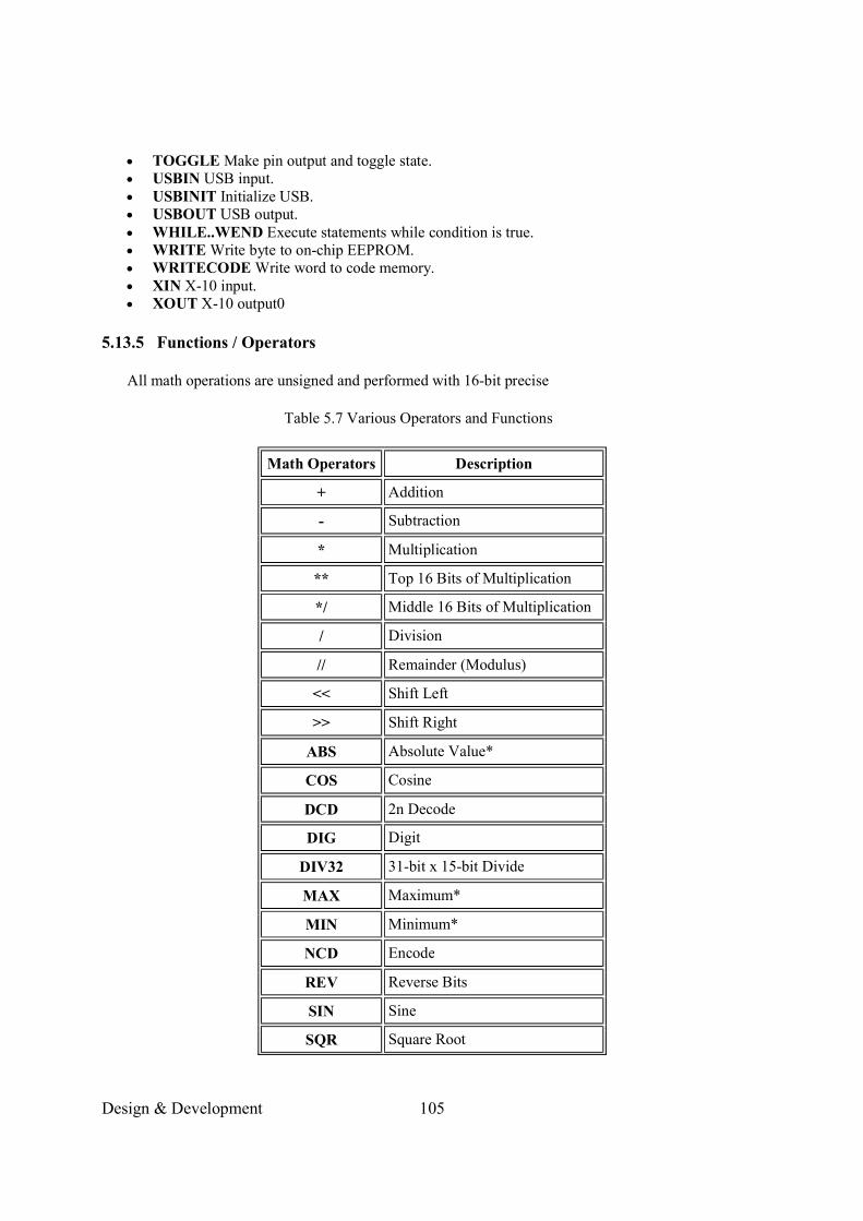
Design & Development 105
TOGGLE Make pin output and toggle state. USBIN USB input. USBINIT Initialize USB. USBOUT USB output. WHILE..WEND Execute statements while condition is true. WRITE Write byte to on-chip EEPROM. WRITECODE Write word to code memory. XIN X-10 input. XOUT X-10 output0
5.13.5 Functions / Operators
All math operations are unsigned and performed with 16-bit precise
Table 5.7 Various Operators and Functions
Math Operators Description
+ Addition
- Subtraction
* Multiplication
** Top 16 Bits of Multiplication
*/ Middle 16 Bits of Multiplication
/ Division
// Remainder (Modulus)
<< Shift Left
>> Shift Right
ABS Absolute Value*
COS Cosine
DCD 2n Decode
DIG Digit
DIV32 31-bit x 15-bit Divide
MAX Maximum*
MIN Minimum*
NCD Encode
REV Reverse Bits
SIN Sine
SQR Square Root

Design & Development 106
Math Operators Description
& Bitwise AND
| Bitwise OR
^ Bitwise Exclusive OR
~ Bitwise NOT
&/ Bitwise NOT AND
|/ Bitwise NOT OR
^/ Bitwise NOT Exclusive OR
5.13.6 Structure of a Compiled Program
PBP is designed to be easy to use. Programs can be compiled and run with little thought to PBP's internal
workings. Some people, however, only have confidence in a product when they understand its internal
workings. Others are just plain curious. It describes the files used and output generated by PBP and gives
some idea of exactly what is going on .
5.13.7 Target Specific Headers
Three target specific header files are used when a program is compiled. One is used by PBP, the other two
are included for use by the assembler. A file with the name of the microcontroller followed by the
extension .BAS contains chip specific information needed by PBP. This includes the memory profile of
the chip, which library it uses, and includes for the definition of the variables it needs. For the
PIC18F2550the default microcontroller, the file is named 16F84.BAS.A file with the name of the
microcontroller followed by the extension .INC is included in the generated .ASM file to give the
assembler information about the chip, including the default configuration parameters (oscillator mode,
Watchdog Timer setting, etc.). For the PIC16F84, the file is named 16F84.INC.Finally, the assembler has
its own include file that defines the addresses of the microcontroller registers. This file is usually named
something on the order of M16F84.INC. and is in the INC directory.
5.13 .8 The Library Files
PBP includes a set of library files that contain all of the code and definition files for a particular group of
microcontrollers. In the case of 14-bit core PIC micros, these files start with the name
PBPPIC14.PBPPIC14.LIB contains all of the assembly language subroutines used by the compiler.
PBPPIC14.MAC contains all of the macros that call these subroutines. Most PICBASIC PRO™
commands consist of a macro and an associated library subroutine. PBPPIC14.RAM contains the VAR
Design & Development 107
statements that allocate the memory needed by the library. PIC14EXT.BAS contains the external
definitions that tell PBP all of the 14-bit core PIC micro register names
5.13.9 PBP Generated Code
A PICBASIC PRO™ compiled program is built in several stages. First PBP creates the .ASM file. It then
builds a custom .MAC file that contains only the macros from the macro library that are used in the .ASM
file. If everything is error free up to this point, it spawns the assembler. The assembler generates its own
set of files. These include the .HEX final output file and possibly listing and debugging files.
5.13.10 ASM File Structure
The ASM file has a very specific structure. Things must be done in a particular order for everything to
work out properly. The first item placed in the file is an equate defining which assembler is to be used,
followed by an INCLUDE to tell the assembler which microprocessor is the target and give it some basic
information, such as the configuration data.Next, all of the variable allocations and aliasing is listed.
EEPROM initialization is next, if called for.An INCLUDE for the macro file is then placed in the file,
followed by an INCLUDE for the library subroutines.Finally, the actual program code is incorporated.
This program code is simply a list of macros that were generated from the PICBASIC PRO™ line.
5. 14 EPIC programmer
EPIC (Explicitly Parallel Instruction Computing) is a 64-bit microprocessor instruction set, jointly
defined and designed by Hewlett Packard and Intel, that provides up to 128 general and floating point unit
registers and uses speculative loading, predication, and explicit parallelism to accomplish its computing
tasks. By comparison, current 32-bit CISC and RISC microprocessor architectures depend on 32-bit
registers, branch prediction, memory latency, and implicit parallelism, which are considered a less
efficient approach in micro architecture design. IA-64 (Intel Architecture-64), Intel's first 64-bit CPU
micro architecture, is based on EPIC. Intel's first implementation, long expected and well-known as
Merced (its code name), was christened with the Itanium brand name in October, 1999. It is expected that
Itanium-based systems will be compatible with versions of existing and future operating systems
including HP-UX, 64-bit Windows, IA-64 Linux, Project Monterey. EPIC programmer consists of
software (EPIC Program) and a programming carrier board (hardware). The EPIC software package has
two executable files one for DOS and another version for Windows. It is the EPIC hardware and software
that take the compiled hex file generated by the compiler and upload it into the microcontroller where it
may be run. The EPIC programmer is compatible with both the PICBasic and PICBasic Pro compilers
[33].

Design & Development 108
5.14.1 EPIC Programmer for PICmicro controllers Features
Low cost programmer for most PICmicro microcontrollers
Connects to PC parallel printer port
ICSP programming
The programmer has a built-on 18-pin socket for programming 8-, 14- and 18-pin DIP packaged
PICmicro MCUs and must be powered with a power adapter within the range of 15 - 18 Volt. (Before
using the programmer be sure to adjust the programming voltage of 13.5 Volt using the mounted
Potentiometer and a Voltmeter) .
5.14.2 EPICWIN and EPIC Programmer
The EPIC Programmer is an inexpensive microcontroller programmer that will program most PIC micro
microcontrollers (MCUs). Most 8-, 14- and 18-pin PIC micro MCUs may be programmed in the socket
on the EPIC Programmer. Optional adapters are available to program 20-, 28- and 40-pin DIP PIC micro
MCUs, as well as PIC micro MCUs in surface-mount and PLCC packages.
5.14.2.1 Software Installation
The EPIC Programmer files are compressed into a self-extracting file on the disk. They must be
uncompressed before use. To uncompress the files, first a directory should be created on hard drive called
EPIC, or any other name.
5.14.2.2 Hardware Installation
There should be no PIC micro MCUs installed in the EPIC programming socket or any connected
adapter's socket until the programming software is executed and the LED is off. The EPIC Programmer
should be placed on an insulated surface to prevent the shorting out of traces on the bottom.T he EPIC
Programmer is connected to a PC compatible parallel printer port using a 25-pin male to 25-pin female
printer extension cable. The EPIC Programmer uses pins 2-6, 10, and 19-25. A serial cable may not have
all of the necessary connections so it should be assured to use a printer extension cable. If the EPIC
Programmer is powered with the optional AC adapter, it should be plugged it into the power connector on
the programmer and then into a wall outlet. The AC adapter should provide approximately 16V DC at
500ma. If the EPIC Programmer is powered with two 9-volt batteries, then batteries should be snapped
onto the battery snaps. 2-pin shorting jumper should be connected to the 2-pin "Batt ON" posts. It is a

Design & Development 109
good idea to check the battery voltage from time to time or if there seems to be difficulty programming
parts. The EPIC Plus Programmer should now be powered up and ready to program PIC micro MCUs.
5.14.3 General Operation
The next task is to write the program using any text editor, such as DOS EDIT or Windows NOTEPAD,
and assemble it using the assembler, PM, included on the disk, or MPASM (or MPLAB), available from
Microchip. Instructions for the use of PM are on the included disk.Once the program assembles properly,
the generated .HEX file may be programmed into a PICmicro MCU using the EPIC programming
software. Three versions of the EPIC software are included: two versions for DOS (one command line
and one graphical) and one for Windows 95/98/ME/NT/2000/XP. The Windows 95/98/ME/NT/2000/XP
version should, of course, be run under Windows 95, 98, ME, NT, 2000 or XP. The Windows and
command line DOS versions are more up-to-date than the graphical DOS version and are able to program
more types of PICmicro MCUs.
5.14.4 EPIC for Windows 95/98/ME/NT/2000/XP
First the Windows 95/98/ME/NT/2000/XP version of the EPIC software should be started by navigating
using Explorer to the EPIC directory and double-clicking on EPICWin. Alternatively, a shortcut can be
created to EPIC on desktop. The EPIC software will take a look around to find where the EPIC Plus
Programmer is attached and get it ready to program a PICmicro MCU. If the EPIC Programmer is not
found, all of the above connections should be checked and verified if there is any PICmicro MCU
installed in the programmer or any connected adapter.Once the programming bar is displayed, the device
type should be selected by using the drop-down device selector box to the right of the buttons.The
assembled object (.HEX) file should be opened. Double-click on the appropriate file to load it. Once the
file has been loaded, the proper device characteristics are selected under the Options menu. The Code
Protect is set to OFF before programming a windowed (JW) PICmicro MCU. Code protected windowed
part may not be erased. A PICmicro MCU sould be inserted into the EPIC Programmer or connected
adapter socket. The end of the PICmicro MCU with the notch should be all the way at the Pin 1 end of the
socket, away from the battery connectors. the Program button should be clicked or Run|Program with the
mouse to program the PICmicro MCU.Before programming, the EPIC software optionally does a blank
check to ensure that the part is erased. If the PICmicro MCU is a 18F2550 or another EEPROM or flash
part, it is usually not necessary to erase it before programming. PIC16F7x and PIC18Fxxx devices do
require erasing each time before the MCU may be reprogrammed
Design & Development 110
5.14.5 EPICWin Controls
The Open speed button opens a .HEX file for programming. The name of an open file appears in the
EPICWin title bar. Previous configuration information will not be altered if Options|Update
Configuration is not checked.
The Save speed button will save the current code, data, ID and configuration information to the
currently open file. If no file has been previously selected, it will prompt for a filename.
The Program speed button will program the current code, data, ID and configuration into the selected
device. It will optionally load the latest version of the .HEX file before programming. The device will be
checked to ensure it is blank before programming, unless Options|Skip Blank Check is checked.
The Verify speed button will compare the current code, data, ID and configuration to the programmed
device. If the information does not match, an error message is displayed. A verify is also done as the
device is being programmed. A code protected device cannot be verified.
The Read speed button will read the current code, data, ID and configuration from the selected device.
The configuration information will not be read if Options|Update Configuration is not checked.
The Blank Check speed button will read the code space to ensure a device is blank. It will not check
the data space, ID, configuration or the oscillator calibration word programmed by the factory into some
devices.
The Erase speed button will erase EEPROM or flash electrically erasable devices. It is grayed out for
devices that cannot be electrically erased.
The Device box allows selection of the device to be programmed. Click the down arrow to the right of the
box to drop down a list of supported devices, and then click on the device. This device information,
including the default device that is selected on start-up, is contained in the file EPIC.INI. This file must be
in the same directory as EPICWIN.EXE. The device should be selected before a .HEX file is opened to
ensure the configuration information is properly interpreted. Devices with parenthesis after them indicate
that they will program either the base version of the part, or the version contained within the parenthesis.

Design & Development 111
5.14.6 EPIC Win Menus
5.14.6.1 File Menu
File|New clears the EPICWin code, data and ID information. If Options|Update Configuration is checked, the configuration information will also be cleared.
File|Open opens a .HEX file for programming. The name of an open file appears in the EPICWin title
bar. Previous configuration information will not be altered if Options|Update Configuration is not
checked.
File|Save saves the current code, data, ID and configuration information to the currently open file. If no file has been previously selected, it will prompt for a filename.
File|EPIC Port will display the parallel printer port the EPIC Programmer was found on, if Auto is checked. If Auto is not checked, the printer port can be selected manually.
File|Exit exits the program.
5.14.6.2 View Menu
View|Code displays the co de wind ow. This will show the open .HEX file or recently read code information in hexadecimal or ASCII.
View|Configuration displays the device configuration fuse window. Additional configuration fuses for the PIC17C7xx and PIC18Xxxx devices must be set from the drop-down Configuration menu.
View|Data EEPROM displays the data EEPROM window. This will show the open .HEX file or recently read data information in hexadecimal or ASCII. Only devices with on-chip EEPROM data space will read and program this data.
View|ID displays the ID window. This will show the open .HEX file or recently read code information in hexadecimal or ASCII.
View|Serial Number displays a window that allows the serial number to be set and programmed into the device. The serial number is stored in the code space at the specified location, overwriting any code that may already be there, and will be incremented by the Increment By value after each successful programming.
View|Count displays a window showing the number of programming attempts and successes. The count is reset when the software is started, a file is opened, a device is read or the device type is changed.
View|Close All Windows closes any open configuration, code, data, ID or count window.
View|Stay On Top causes the EPICWin bar to float on top of any other windows when checked.

Design & Development 112
5.14.6.3 Run Menu
Run|Program will program the current code, data, ID and configuration into the selected device. It will optionally load the latest version of the .HEX file before programming. The device will be checked to ensure it is blank before programming, unless Options|Skip Blank Check is checked.
Run|Verify will compare the current code, data, ID and configuration to the programmed device. If the information does not match, an error message is displayed. A verify is also done as the device is being programmed. A code protected device cannot be verified.
Run|Read will read the current code, data, ID and configuration from the selected device. The configuration information will not be read if Options |Update Configuration is not checked.
Run|Blank Check will read the code space to ensure a device is blank. It will not check the data space, ID, configuration or the oscillator calibration word programmed by the factory into some devices.
Run|Erase will erase EEPROM or flash electrically erasable devices. It is grayed out for devices that cannot be electrically erased.
5.14.6.4 Configuration Menu
The configuration fuses are unique to each particular PICmicro MCU.
5.14.6.5 Options Menu
Options|Program/Verify Code allows the device's code space to be programmed and verified when checked. If it is not checked, the device's code space will not be programmed or verified. It will always be read and blank checked, regardless.
Options|Program/Verify Configuration allows the device's configuration fuses to be programmed and verified when checked. If it is not checked, the device's configuration fuses will not be programmed or verified.
Options|Program/Verify Data allows the device's data space, if any, to be programmed and verified when checked. If it is not checked, the device's data space will not be programmed or verified. It will always be read, regardless.
Options|Program/Verify ID allows the device's ID to be programmed and verified when checked. If it is not checked, the device's ID will not be programmed or verified. It will always be read, regardless.
Options|Program/Verify Oscillator Calibration allows the device's oscillator calibration factor location to be programmed and verified when checked. If it is not checked, the device's oscillator calibration factor location will not be programmed or verified. It will always be read, regardless.
Options|Program Serial Number allows a serial number to be programmed into the device when checked. If it is not checked, the serial number will not be programmed. As the serial number is programmed into the code space, Program Code must also be checked to program the serial number.
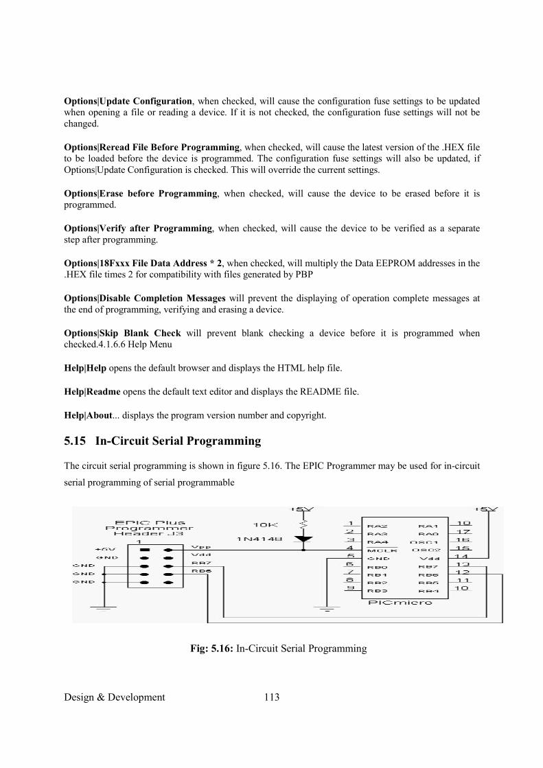
Design & Development 113
Options|Update Configuration, when checked, will cause the configuration fuse settings to be updated when opening a file or reading a device. If it is not checked, the configuration fuse settings will not be changed.
Options|Reread File Before Programming, when checked, will cause the latest version of the .HEX file to be loaded before the device is programmed. The configuration fuse settings will also be updated, if Options|Update Configuration is checked. This will override the current settings.
Options|Erase before Programming, when checked, will cause the device to be erased before it is programmed.
Options|Verify after Programming, when checked, will cause the device to be verified as a separate step after programming.
Options|18Fxxx File Data Address * 2, when checked, will multiply the Data EEPROM addresses in the .HEX file times 2 for compatibility with files generated by PBP
Options|Disable Completion Messages will prevent the displaying of operation complete messages at the end of programming, verifying and erasing a device.
Options|Skip Blank Check will prevent blank checking a device before it is programmed when checked.4.1.6.6 Help Menu
Help|Help opens the default browser and displays the HTML help file.
Help|Readme opens the default text editor and displays the README file.
Help|About... displays the program version number and copyright.
5.15 In-Circuit Serial Programming
The circuit serial programming is shown in figure 5.16. The EPIC Programmer may be used for in-circuit
serial programming of serial programmable
Fig: 5.16: In-Circuit Serial Programming

Design & Development 114
PICmicro MCUs through the 10-pin expansion header J3. Vpp, RB6, RB7 and ground should be
connected as in the following diagram. Any additional connections to /MCLR, RB6 and RB7 should be
designed as to not interfere with in-circuit programming. The cable connecting the EPIC 10-pin header to
the target board should be less that 6 inches long. The drawing shows the pinouts and connections to the
18-pin PIC18F2550 For other PIC MCUs, use their corresponding pin connections.Note: +5 volts should
be supplied to the PICmicro MCU by the target system. The +5 volt and Vdd lines from the EPIC Plus
Programmer header are not intended to power external circuits.
5.16 Photograph /Bottom view/Layout of the System
The photograph of the system are shown in figure 5.17(a) and figure5.17(b)
Fig. 5.17(a): Front Photograph of the Prototype in functional state

Design & Development 115
Fig.5. 17(b): Bottom View of the System
Result & Verification 116
CHAPTER -6 RESULT AND VERIFICATION
6.1 Objectives
The objectives of the thesis are as follows:
To develop the system with reducing cost and sending the energy meter reading from
consumers residence and receiving it into database server of organization using SMS
technology
Digital energy meter reading will be sent without involvement of human being into the
database server of organization at the starting day of a month.
No meter reader is to be involved for taking the meter reading
The organization will be benefited.
The organization will be corruption free and system loss will be reduced.
The skilled technical persons will be involved with the system.
The accuracy of the meter reading system will be maintained
The reputation of the organization will be enhanced.
Friendly relationship will be established between consumers and organization.
6.2 Required Equipments
6.2.1 Hardware Components
Energy Measuring Chip
Microcontroller
GSM Module
SIM
LCD Display/Monitor
EPIC Programmer board
DC Power Supply(X –former ,IC, Transistor and Capacitor)
Test Board
6.2.2 Software Components
EPIC Win

Result & Verification 117
PIC Basic Pro Software
6.3 Circuit Diagram
The schematic circuit diagram of the system is shown in figure 6.1. The basic parameters of this
circuit are microcontroller, GSM module, Energy Measuring Chip, LCD display and some
interfacing circuits.
Fig. 6.1: Schematic circuit Diagram
In this system microcontroller acts as a brain and control the operation of the whole system using
fixed program that is stored in memory.

Result & Verification 118
6.4 Operation
The figure 6.1 represents the schematic circuit diagram of the system. It’s a microcontroller
based system and microcontroller controls the interfacing equipments functions using fixed
program that is stored in memory. The desire output of the system is to produce data reading in
energy form continuously and sending this reading to the organization at the first day of a month
by SMS method.. The operating mechanism of the system such as energy measuring chip of
digital energy meter produces serial energy data output from analog input by the sequential
action of its consisting parameters that are serially interfaced to the microcontroller.
Microcontroller reads energy data from energy measuring chip .Later microcontroller
accumulate data, calculate data, store data in EEPROM and display data reading on LCD
display each 10 second later. Microcontroller reads time from GSM network via GSM module
and compares this time with setting time. At the starting moment of a month the receiving time
must be equal the setting time according to program and microcontroller provides data reading to
GSM module. The initially microcontroller send previous reading and later send current reading.
GSM module reads data, produce short message on the basis of reading and send message
through mobile communication system. Later the SMS message in GSM Module is deleted by
microcontroller and the meter reading is received by organization server via mobile
communication system such a sequence that means GSM module- BTS-BSC-MSC -GMSC-
MSC-BSC-BTS- Modem - SMS enabler software-database server-1 –SQL-database server-2. .
In fact microcontroller communicates with other equipments in this system by some interfacing
circuits. The basic functions of the interfacing circuits in this system such as
Using Q1 transistor based interfacing circuit microcontroller power on to the GSM
module.
Using Q2 transistor based interfacing circuit GSM module acknowledges to the
microcontroller.
Using zener diode based interfacing circuit microcontroller provides meter reading /
request signal to the GSM module.
Using Q4 & Q5 transistors based interfacing circuit GSM module acknowledgement to
the microcontroller

Result & Verification 119
Using Q3 Transistor based interfacing circuit GSM module takes network information.
The firstly blinking of GSM module LED indicates that the network is not available and
normal blinking of LED indicates that the network is available.
Using Q6 transistor based interfacing circuit microcontroller controls the load
connection with the system.
It may be noted that while microcontroller providing the data reading to the GSM module, if the
electricity is not available then the message sending will be remained stop. Later when the
electricity will come in that case the first priority basic the microcontroller will provide the data
reading to the GSM module and GSM module will do the as usual functions.
6.5 Result
When power supply provided to the circuit, the circuit activated effectively. The Microcontroller
provided the meter reading to the LCD display unit each 10 second later.. Microcontroller
provides the meter reading to the GSM module at the first day of the month. .GSM Module
received the meter reading and produced short message on the basic of meter reading and sent
message through mobile communications systems.
6.6 Discussion
Completed the all works with carefully for achieving the desired result. The system was basically
microcontroller based and microcontroller controls the function of all the equipments. The result
of the work i.e, the digital energy meter reading from the consumer meter was sent to the
organization server using SMS technology. For achieving the desire result, we designed circuit,
wrote program, compiled program and installed program into microcontroller. Later assembled
all hardware components in circuit diagram and was made the connection properly. Lastly it was
produced the net output of the system.

120
CHAPTER-7
ENERGY METER READING TRANSFER TO BILLING STATION 7.1 Introduction This is the time of information technology. In the era of advancement it is possible to send and receive energy meter reading from one to another end of the world in a very short time with minimum cost. In early days due to lack of man power, lack of responsibilities of concern person, unfavorable weather and communication it would not be possible to send this reading from one place to another. In that case people would face a lot of problems and they would deprive from various type of services. For getting the better services mobile phone data communication system and computer may provide massive contribution .In fact now a days the use of mobile phone data communication and computer has been increased that has positively affected the human civilization. In some cases for getting the desired result the mobile phone data communication system and the data terminal equipment are used simultaneously. From data terminal equipment it is possible to send desired data through mobile phone system. Consequently it is also possible to send the data reading to the computer and save corresponding energy consumed reading into the database server in a secured manner. In fact for taking the energy meter reading from GSM network and saving this reading into database server in that case over all work is accomplished by the sequential action of GSM modem, SMS Enabler Software and SQL(Structured Query Language) respectively. 7.2 System Architect of Energy Meter Reading Save into Database Server The figure 7.1 represents the system architect of energy meter reading loading system into database server. The system is composed of GSM network, GSM modem, SMS Enabler Software, database server-1,SQL (Structured, Query Language)and database server-2 parameter. The operating principle of the system such as GSM modem reads the energy meter reading, sender number and time from the GSM network and save these parameters into the SIM or other memory location of this device.
Fig. 7.1: Block Diagram of the System
SMS
Enabler
Software
Database
Server-1
Modem
Energy Meter Reading
SQL Database
Server-2
GSM Network PC

121
Later it is needed to transfer the above mentioned parameters from the SIM to database server-1 In that case SMS Enabler Software is used for accomplishing this work. In fact SMS Enabler Software reads energy meter reading, sender number and time from SIM and load these parameters into the database server-1 corresponding to the column name. Again it is needed to transfer energy meter reading (For sorting the previous kwh, current kwh and prepare net kwh), sender number and time to the database server-2 according to column name from data base server-1. In that case SQL (Structured, Query Language) is used for performing this work. 7.3 Software used for Processing the Energy Meter Reading into Database Server
SMS Enabler Software SQL (Structured Query Language)
7.4 Utility of SMS Enabler Software for processing the Energy Meter Reading SMS Enabler is a multi purpose usable software that supports multiple functions. SMS Enabler is a computer program that automatically support to receive incoming energy meter reading from GSM network using an attached GSM modem to PC .SMS Enabler can a) automatically save, incoming energy meter reading into a database according to desired format. b) forward incoming energy meter reading to a web server via HTTP; c) forward, incoming energy meter reading as emails d) save incoming energy meter reading to a text file(s); 7.5 Key Feature of SMS Enabler Software
The complete feature of SMS Enabler Software are given below: SMS Enabler Software-
Uses a GSM modem, connected to a computer, to receive SMS messages and send replies. The phone/modem can be connected to a PC via cable, Bluetooth or infrared (IR).
Supports automatic saving of received SMS text messages into a database. Supports MS Access, MS SQL Server, My SQL, Oracle databases, as well as other databases through ODBC or OLE DB drivers.
Supports automatically dispatching received SMS text messages to a web server via HTTP, so those messages can be handled by a server-side script. The script can be written in any web programming language, such as PHP, ASP.NET and so forth. Secure HTTP (HTTPS) is also supported.
Supports automatic forwarding of received SMS text messages as email messages to one or more addresses using the SMTP protocol. Messages can

122
be forwarded to different email addresses depending on the content of the message and/or the sender's number.
Allows incoming SMS messages to be automatically saved into a text/CSV file, or multiple files, for real-time processing and logging. Three modes are supported: a) 'single file'; b) 'file per day'; and c) 'file per message'.
Supports automatic SMS message reply to the sender. The reply message text can be predefined in the settings, or generated dynamically by a web script.
Designed to run continuously without user intervention. Automatically reconnects to the phone/modem upon loss of connection. Supports long (linked/concatenated) messages. Supports Unicode SMS messages Logging Supports Windows 2000, Windows XP, Windows Vista, Windows 7, and
Windows Server 2003/2008.
7.6 Utility of SQL for Reformatting the Energy Meter Reading Data into Database Server Structured Query Language is a programming language designed for managing data in relational database management systems (RDBMS).Originally based upon relational algebra and tuple relational calculus, its scope includes data insert, query, update and delete, schema creation and modification, and data access control. Structured Query Language makes relationship between two or more database server in case of data transaction. In this system energy meter reading data firstly store into database server-1 and later store into database server-2 according to desire format. In fact there are two parts of the energy meter reading. One is previous reading and another is current reading.It is needed to be shown in database server-2 in separate mode and prepare net meter reading. This work is accomplished by query operation of Structured Query Language . 7.6.1 Query of Structured Query Language The most common operation in SQL is the query, which is performed with the declarative SELECT statement. SELECT retrieves data from one or more tables, or expressions. Standard SELECT statements have no persistent effects on the database. Some non-standard implementations of SELECT can have persistent effects, such as the SELECT INTO syntax that exists in some databases. Queries allow the user to describe desired data, leaving the database management system (DBMS) responsible for planning, optimizing, and performing the physical operations necessary to produce that result as it chooses.A query includes a list of columns to be included in the final result immediately following the SELECT keyword. An asterisk ("*") can also be used to specify that the query should return all columns of the queried tables. SELECT is the most complex statement in SQL, with optional keywords and clauses that include:

123
The FROM clause which indicates the table(s) from which data is to be retrieved. The FROM clause can include optional JOIN subclauses to specify the rules for joining tables.
The WHERE clause includes a comparison predicate, which restricts the rows returned by the query. The WHERE clause eliminates all rows from the result set for which the comparison predicate does not evaluate to True.
The GROUP BY clause is used to project rows having common values into a smaller set of rows. GROUP BY is often used in conjunction with SQL aggregation functions or to eliminate duplicate rows from a result set. The WHERE clause is applied before the GROUP BY clause.
The HAVING clause includes a predicate used to filter rows resulting from the GROUP BY clause. Because it acts on the results of the GROUP BY clause, aggregation functions can be used in the HAVING clause predicate.
The ORDER BY clause identifies which columns are used to sort the resulting data, and in which direction they should be sorted (options are ascending or descending). Without an ORDER BY clause, the order of rows returned by an SQL query is undefined
7.7 Method of Loading Energy Meter Reading into a Database Server using SMS Enabler Software
SMS Enabler can automatically save incoming energy meter reading directly into a MS Access database. In order to configure SMS Enabler to forward incoming energy meter reading into a MS Access database, it is needed to:(a) create a special table named SMS_IN in database (SMS_IN will store received energy meter reading);(b) specify the connection parameters to database in the settings dialog box in SMS Enabler. The information given below on how to configure SMS Enabler Software with a Microsoft Access database For creating a table named SMS_IN in database to store incoming energy meter reading .
Table 7.1 Format of Database server
SMS_IN Column name Type Description
SMS_TEXT Memo message content SENDER_NUMBER
Text sender's number
SENT_DT Date/time the time when the sender sent the message
It may be configured database connection parameters in SMS Enabler's settings dialog box. Later the setting dialog box may be opened in SMS Enabler and selecting the energy meter reading to database page. It may be checked the save

124
received energy meter reading into a database checkbox. It may be clicked to create connection string, and select Microsoft Access in the menu. A dialog box will open where it can be specified the path to database file(SMS_IN)
Settings dialog box Connection
Modem connection: It may be selected which modem/phone want to use with SMS Enabler, or via which COM port this modem/phone is connected to PC.
Baud rate it may be entered the baud rate to use to connect to modem/phone, or select the appropriate value from the list.
RTS/CTS flow control ; It may be selected "On" to enable RTS/CTS flow control. Auto start SMS Enabler to automatically start receiving when it launches. Save received energy meter reading into a database: SMS Enabler to
automatically save incoming energy meter reading into a database.

125
Connection string :A connection string is a string that specifies information about a data source and the means of connecting to it. It may be created connection string' for a MS Access database,
String encoding : It may be Specifies which encoding is used to save string data into the database.
Maximum number of retries: The maximum number of attempts to save a received energy meter reading into the database, after the first attempt fails.
Retry timeout (in seconds) The number of seconds to wait before retrying, if the previous attempt to save a received energy meter reading into the database
7.8 Transfer Data from Database Server-1 to Database Server-2 Using SQL (Structured Query Language )
The table [7. 2] represents the format of database server-1 and file name of the format is SMS_IN. This table contains three columns where the column name sms_text, sender_number and sent_dt respectively. The energy meter reading load into first column, sender number load into second column and time load into third column from GSM network via GSM Modem and SMS Enabler software.

126
Table 7.2 Energy Meter Reading Load into Database server-1
SMS_IN sms_text sender_number sent_dt
previous kwh=0.002606 recent kwh=0.004178 01933480062 1/10/2011 10:11:00 AM previous kwh=0.002609 recent kwh=0.004180 01718207476 1/10/2011 11:15:00 AM previous kwh=0.002611recent kwh=0.004180 01718891619 1/10/2011 12:10:00 PM
For transferring data according to sorting base from database server-1 to database server-2, a query has been written in SQL that is shown in double star mark. ***INSERT INTO Meter_Reading INSERT INTO Meter_Reading ( Previous_kwh, Current_kwh, Net_kwh, sender_number, sent_dt ) SELECT Mid([sms_text],14,8), Mid([sms_text],34,8), Mid([sms_text],34,8)-Mid([sms_text],14,8), sender_number, sent_dt FROM SMS_IN; ;*** Only opening the query and all data transfer from database server-1 to database server-2 according to sorting. The result of the operation is shown in table[ 7 .3]. The table 2 represents the format of database server-2 and file name of the format is Meter_Number. This table contains five columns where the column name Previous_kwn, Current_kwh, Net_kwh ,sender_number and sent_dt respectively.
Table7.3 Energy Meter Reading Load into Database server-2
.
Meter_Reading Previous_kwh Current_kwh Net_kwh sender_number sent_dt
0.002606 0.004178 0.001572 01933480062 1/10/2011 10:11:00 AM 0.002609 0.004180 0.001571 01718207476 1/10/2011 11:15:00 AM 0.002611 .004180 0.001569 01718891619 1/10/2011 12:10:00 PM

Discussion 127
CHAPTER-8 DISCUSSION
The fundamental work of the thesis includes generation, transmission, and reception of digital
energy meter reading into database server for providing the better service to the consumer and
secondary aim of this thesis is to reduce cost, remove corruption, produce job opportunity for the
skilled technical person, overcome the system loss, increase reputation of organization and
finally make friendly relationship between consumers and organization .
The reason for doing this work was that there are three types of energy meter reading systems
available in Bangladesh, such as analog energy meter, digital energy meter and digital prepaid
energy meter reading system. In case of analog energy meter and digital energy meter reading
system, a meter reader has to be attended in front of meter at the end of month or any specific
date of the month for taking the meter reading .Sometimes they can not take the meter reading
timely due to lack of man power, due to lack of negligence, unfavorable weather and
communication. In that case system loss increases and negatively influences the organization.
Whereas in case of digital prepaid meter system, meter card has to be installed into the meter.
When book value of the card is equal to the energy consumed by the meter then meter
automatically shuts down. Later, meter card has to be purchased from the market or
organization. But sometimes meter cards are not available in the market and the consumer faces
automatic trouble of load shedding. Not only that there is a common practice in Bangladesh that
the meter readers and also consumers are involved in illegal procedure and corruption. The
corruption of meter readers and consumers are considered as system loss by authority that has
also negative influence on the organization and therefore, the reputation of the organization will
be reduced. GSM and SMS technology which have been utilized in this thesis work reliably and
confidentially and provides the better service.
8.1 Limitation
The limitation of the thesis work are as follows:
The digital energy meter will be installed in such a place where the network should be
available. Because without mobile network, it is not possible to send energy meter
reading to the organization server from consumer residence by SMS method.

Discussion 128
The digital energy meter will be installed in such a place where the temperature should
remain within reasonable range to be matched with the equipment. Otherwise
microcontroller may do malfunctions.
The price of the microcontroller based main circuit is too high. Actually GSM module is
an additional part of the consumer meter. It is much difficult to purchase the meter for
those who are poor consumers. So It should be provided by organization.
The Microcontroller based main circuit is sensitive as it may be damaged by mishandling.
Overall system function depends upon hardware and software. So any problem of the two
items, system may face interruption for generation and transmission of short message.
Those who are illiterate consumers firstly may accept the meter reading by SMS method
with confusion. In that case, it is needed to motivate them by the organization.
8.2 Achievement
The achievement of the thesis is to receive the digital energy meter reading into database server
sent from the consumers premises. This result has already been achieved in the present work.
Before achieving this result, some knowledge on purely dc power supply production, equipment,
digital energy meter mechanism, microcontroller mechanism, GSM module, SIM, GSM
technology, SMS technology, programming language and also software function have to be
achieved. On the basis of this achievement, a lot of options are available for the extension of
future works.
8.3 Recommendation for Future Work
In extension of future work, it is possible to disconnect load from meters from organization if the consumers are not found to pay the bill in time or for doing any offensive work that is not certified by the electricity supply authority. As an extension of future work it is possible to prepare electricity bill by utilizing the recent SMS energy meter reading in database server and sends to the consumers mobile where the present status of the meter reading can be checked instantaneously.
-End-
References 129
References [1] GSM Module: GSM Notification Module http://www.g-e.ee/files/manuals/gsm- n2_eng.pdf/
(Accessed on 16th June 2009).
[2] Trosby F. SMS,thestrage duckling of GSM.Telekronikk; 2004;3:pp187-194
[3] Remote Meter system, Meterhttp://homepage.usask.ca/~tak488/SMS_Remote Meter.pdf
(11-11-2009)
[4] Global System for Mobile Communication http://en.wikipedia.org/wiki/GSM(03 11 2009)
[5] Short Message Service http://en.wikipedia.org/wiki/Short_message_service(03-11-2009). [6] Microcontroller http://en.wikipedia.org/wiki/Microcontroller(18-10-009 ) [7] PIC Microcontroller http://en.wikipedia.org/wiki/PIC_microcontroller(18-10-009 ) [8] SIM http://en.wikipedia.org/wiki/Subscriber_Identity_Module(18-10-009) [9] Energy meter http://en.wikipedia.org/wiki/Energy_meter(18-10-009)
[10] LCD http://en.wikipedia.org/wiki/Liquid_crystal_display(19-10-009) [11] PIC BASIC PRO SOFTWARE http://www.warburtech.com/compilers/picbasic.pro/
(02-011-2009) [12] EPIC Win Software, Ford Equity Research. EPIC for Windows v5.00 – Download and
Install Instructions http://www.fordupdate.com/epic.htm//(Accessed on 17th June 2009). [13] SMS Enabler Software www. smsenabler.com(Accessed on 03.06.2011) [14] Structured Query Language http://en.wikipedia.org/wiki/ Structured _ Query _ Language
(Accessed on 16.05.2011)
[15] SMS what where and how http://www.wirelessdevnet.com/channels/sms/features/sms. html (27-10-2009)
[16] GSM BASIC http://media.wiley.com/product_data/excerpt/49/04700169/0470016949.pdf
(25-10-009).
[17] Introduction to SMS Technology.com.hk/document/networking/sms_via_email.pdf (27-10-2009
[18] SMS protocol http://www.3gpp2.org/Public_html/specs/CS0015-0.pdf(5-11-2009)
[19] gsm user service http://www.tutorialspoint.com/gsm/ gsm_user_services .htm (05- 11-2009) [20] GSM Specification http://www.tutorialspoint.co m/gsm/gsm_specification.htm (5-11-2009)
[21] Microcontroller Basic Stam http://a.parsons.edu/~cherdlick/courses/archInt_stamp

References 130
.pdf-(08-11-2009
[22] Programming Pic Microcontroller http://seniord.ece.iastate.edu/dec0604/ index_files/ tutorialDec0604.pdf(08-11-2009)
[23] Karataş P, Aksoy M. Microcontroller based Home Automation. Proceedings of
International Conference on Intelligent Knowledge Systems (IKS-2004), 16-20
August, 2004. http://www Ikss.org/iks-2004/pdf/E0109.pdf//(Accessed on 17th
June 2009).
[24] Microcontroller Features http://www.esacademy.com/automation/faq/primer/4.htm (08-11-220)
[25] Microcontroller http://ww1.microchip.com/downloads/en/ DeviceDoc/39632D
.pdf (20-10-009)
[26] Energy Measuring Chip(ADE7756) analog.com/static/importedfiles/product_ highlights/828090860_features_2003New.pdf (Accessed on13-10-2009)
[27] ADE7756AN Energy Measuring Chip http://pdf1.alldatasheet.com/datasheetpdf/
view/113531/AD/ADE7756AN.html
[28] Power Supply Technical Guide. http://www.xppower.com/ (Accessed on 26th June
2009).
[29] SIM Technology Group Ltd. Wireless Module Solution. http://www.sim.com/
(Accessed on 22nd June 2009).
[30] Amphenol Smart Card Connectors.: http:// www.mouser.com/amphenol-tuchel/
(Accesed on 22nd June 2009).
[31] Gray GW, Kelly SM. Liquid crystals for twisted nematic display devices. Journal
of Material Chemistry. 1999; Vol. 9: pp. 2037-2050.
[32] PICBASIC Compiler. http:// www.melabs.com/ (Accessed on 30th June 2009)
[33] PICBASIC Pro Compiler http://www.imagesco.com/microcontroller/pbpman.pdf//
(Accessed on 17th June 2009).