Master Components Selector Guide - 7magico
277
SG388/D Rev. 1, Aug-1999 Master Components Selector Guide ON Semiconductor Formerly a Division of Motorola
-
Upload
khangminh22 -
Category
Documents
-
view
2 -
download
0
Transcript of Master Components Selector Guide - 7magico
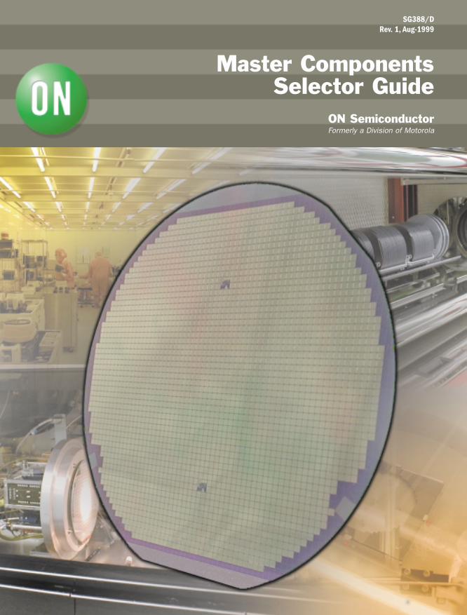
SG388/DRev. 1, Aug-1999
Master ComponentsSelector Guide
ON SemiconductorFormerly a Division of Motorola
ON Semiconductor and are trademarks of Semiconductor Components Industries, LLC (SCILLC). SCILLC reserves the right to make changes without further notice to any products herein. SCILLC makes no warranty, representation or guarantee regarding the suitability of its products for any particular purpose, nor does SCILLC assume any liability arising out of the application or use of any product or circuit, and specifically disclaims any and all liability, including without limitation special, consequential or incidental damages. “Typical” parameters which may be provided in SCILLC data sheets and/or specifications can and do vary in different applications and actual performance may vary over time. All operating parameters, including “Typicals” must be validated for each customer application by customer’s technical experts. SCILLC does not convey any license under its patent rights nor the rights of others. SCILLC products are not designed, intended, or authorized for use as components in systems intended for surgical implant into the body, or other applications intended to support or sustain life, or for any other application in which the failure of the SCILLC product could create a situation where personal injury or death may occur. Should Buyer purchase or use SCILLC products for any such unintended or unauthorized application, Buyer shall indemnify and hold SCILLC and its officers, employees, subsidiaries, affiliates, and distributors harmless against all claims, costs, damages, and expenses, and reasonable attorney fees arising out of, directly or indirectly, any claim of personal injury or death associated with such unintended or unauthorized use, even if such claim alleges that SCILLC was negligent regarding the design or manufacture of the part. SCILLC is an Equal Opportunity/Affirmative Action Employer.
USA/EUROPE Literature Fulfillment:Literature Distribution Center for ON SemiconductorP.O. Box 5193, Denver, Colorado 80217 USAPhone: 303-675-2175 or 800-344-3860 Toll Free USA/CanadaFax: 303-675-2176 or 800-344-3867 Toll Free USA/CanadaEmail: [email protected]
Fax Response Line: 303-675-2167800-344-3810 Toll Free USA/Canada
N. Amercian Technical Support: 800-282-9855 Toll Free USA/Canada
ASIA/PACIFIC: LDC for ON Semiconductor - Asia SupportPhone: 303-675-2121 (Tue-Fri 9:00am to 1:00pm Hong Kong Time)Email: [email protected]
JAPAN: ON Semiconductor, Japan Customer Focus Center4-32-1 Nishi-Gotanda, Shinagawa-ku, Tokyo, Japan 141-8549Phone: 81-3-5487-8345Email: [email protected]
ON Semiconductor Website: http://onsemi.com
For additional information, please contact your local Sales Representative
PUBLICATION ORDERING INFORMATION
SG388/D
ON
Sem
iconducto
rM
aster C
om
ponents S
ele
ctor G
uid
e
ON Semiconductor Components Selector Guide
Analog, Logic and Discretes Products
SG388/DRev. 1, Aug–1999

Contents
Analog 3. . . . . . . . . . . . . . . . . . . . . . . . . . . . . . . . . . . . . . . . . . . . . . . . . . . . . . . . . . . . . . Logic 115. . . . . . . . . . . . . . . . . . . . . . . . . . . . . . . . . . . . . . . . . . . . . . . . . . . . . . . . . . . . . . . Discretes 145. . . . . . . . . . . . . . . . . . . . . . . . . . . . . . . . . . . . . . . . . . . . . . . . . . . . . . . . . . . .
Small Signal Transistors, FETs and Diodes 145. . . . . . . . . . . . . . . . . . . . . . . . . . . . TVS/Zeners, Transient Voltage Suppressors (TVS)Regulator Diodes 161. . . . . . . . . . . . . . . . . . . . . . . . . . . . . . . . . . . . . . . . . . . . . . . . . .
TMOS Power MOSFETs 183. . . . . . . . . . . . . . . . . . . . . . . . . . . . . . . . . . . . . . . . . . . . Bipolar Power Transistors 194. . . . . . . . . . . . . . . . . . . . . . . . . . . . . . . . . . . . . . . . . . . Rectifiers 204. . . . . . . . . . . . . . . . . . . . . . . . . . . . . . . . . . . . . . . . . . . . . . . . . . . . . . . . . . Thyristors, Triggers and Surge Suppressors 216. . . . . . . . . . . . . . . . . . . . . . . . . . . IGBT Products 234. . . . . . . . . . . . . . . . . . . . . . . . . . . . . . . . . . . . . . . . . . . . . . . . . . . . .
Alphanumeric Parts Index 247. . . . . . . . . . . . . . . . . . . . . . . . . . . . . . . . . . . . . . . . . . . . . Alphabetical Subject Index 272. . . . . . . . . . . . . . . . . . . . . . . . . . . . . . . . . . . . . . . . . . . .
USA/EUROPE Literature Fulfillment:Literature Distribution Center for ON SemiconductorP.O. Box 5163, Denver, Colorado 80217 USAPhone: 303–675–2175 or 800–344–3860 Toll Free USA/CanadaFax: 303–675–2176 or 800–344–3867 Toll Free USA/CanadaEmail: [email protected]
Fax Response Line*: 303–675–2167800–344–3810 Toll Free USA/Canada*To receive a Fax of our publications
N. America Technical Support: 800–282–9855 Toll Free USA/Canada
ON Semiconductor and are trademarks of Semiconductor Components Industries, LLC (SCILLC). SCILLC reserves the right to makechanges without further notice to any products herein. SCILLC makes no warranty, representation or guarantee regarding the suitability of its productsfor any particular purpose, nor does SCILLC assume any liability arising out of the application or use of any product or circuit, and specifically disclaimsany and all liability, including without limitation special, consequential or incidental damages. “Typical” parameters which may be provided in SCILLCdata sheets and/or specifications can and do vary in different applications and actual performance may vary over time. All operating parameters,including “Typicals” must be validated for each customer application by customer’s technical experts. SCILLC does not convey any license underits patent rights nor the rights of others. SCILLC products are not designed, intended, or authorized for use as components in systems intended forsurgical implant into the body, or other applications intended to support or sustain life, or for any other application in which the failure of the SCILLCproduct could create a situation where personal injury or death may occur. Should Buyer purchase or use SCILLC products for any such unintendedor unauthorized application, Buyer shall indemnify and hold SCILLC and its officers, employees, subsidiaries, affiliates, and distributors harmlessagainst all claims, costs, damages, and expenses, and reasonable attorney fees arising out of, directly or indirectly, any claim of personal injury ordeath associated with such unintended or unauthorized use, even if such claim alleges that SCILLC was negligent regarding the design or manufactureof the part. SCILLC is an Equal Opportunity/Affirmative Action Employer.
PUBLICATION ORDERING INFORMATIONASIA/PACIFIC: LDC for ON Semiconductor – Asia SupportPhone: 303–675–2121 (Tue–Fri 9:00am to 1:00pm, Hong Kong Time)Email: ONlit–[email protected]
JAPAN: ON Semiconductor, Japan Customer Focus Center4–32–1 Nishi–Gotanda, Shinagawa–ku, Tokyo, Japan 141–8549Phone: 81–3–5487–8345Email: [email protected]
ON Semiconductor Website: http://onsemi.com
For additional information, please contact your local Sales Representative.

ON Semiconductor Selector Guide – Analog Integrated Circuits
http://onsemi.com 3
Analog Integrated Circuits
In Brief . . .ON Semiconductor Analog Integrated Circuits cover a
much broader range of products than the traditional opamps/regulators/consumer–image associated with Analogsuppliers. Analog circuit technology currently influencesthe design and architecture of equipment for all majormarkets. As with other integrated circuit technologies,Analog circuit design techniques and processes have beencontinually refined and updated to meet the needs of thesediversified markets.
Operational amplifiers have utilized SMARTMOStechnology for improved performance, plus innovativedesign and trimming concepts have evolved for improvedhigh performance and precision characteristics. In analogpower ICs, basic voltage regulators have been refined toinclude higher current and voltage levels, low dropout reg-ulators, CMOS technology, and more precise three–termi-
PageSignal Conditioning 5. . . . . . . . . . . . . . . . . . . . . . . . . . . . . Battery Management 14. . . . . . . . . . . . . . . . . . . . . . . . . . . Power Management 20. . . . . . . . . . . . . . . . . . . . . . . . . . . System Management 87. . . . . . . . . . . . . . . . . . . . . . . . . . Motor Control 94. . . . . . . . . . . . . . . . . . . . . . . . . . . . . . . . . Interface 101. . . . . . . . . . . . . . . . . . . . . . . . . . . . . . . . . . . . Other Circuits 104. . . . . . . . . . . . . . . . . . . . . . . . . . . . . . . .
nal fixed and adjustable voltages. The power area contin-ues to expand into switching regulators, power supplycontrol and supervisory circuits, motor controllers, andbattery charging controllers and protection circuits.
The table of contents provides a perspective of themany markets served by Analog ICs and ofON Semiconductor’s involvement in these areas.
ANALOG INTEGRATED CIRCUITS
SIGNALCONDITIONING
BATTERYMANAGEMENT
POWERMANAGEMENT
SYSTEMMANAGEMENT
MOTORCONTROL INTERFACE OTHER
CIRCUITS
Op–Amps
Comparators
LithiumBattery
ProtectionICs
ChargeControllers
DC–DCConverters
with Inductor
Off–LineSMPS
Controllers
UndervoltageSupervisory
OvervoltageSupervisory
DataTransmission
DisplayDrivers
Timers
Linear Four–QuadrantMultiplier
Power FactorControllers
VoltageReferences
Linear VoltageRegulators
LDO LinearVoltage
Regulators
MOSFET/IGBT Drivers
DedicatedDrivers
Dedicated PowerMgmnt Controllers
DC MotorControl

ON Semiconductor Selector Guide – Analog Integrated Circuits
http://onsemi.com 4
SIGNAL CONDITIONING 5. . . . . . . . . . . . . . . . . . Operational Amplifiers 6. . . . . . . . . . . . . . . . . . . . . . . . . . .
Single 6. . . . . . . . . . . . . . . . . . . . . . . . . . . . . . . . . . . . . . Dual 7. . . . . . . . . . . . . . . . . . . . . . . . . . . . . . . . . . . . . . . Quad 9. . . . . . . . . . . . . . . . . . . . . . . . . . . . . . . . . . . . . . . One Volt SMARTMOS Rail–to–Rail Dual Operational Amplifier 11. . . . . . . . . . . . . . . . . . . . . . .
Miscellaneous Amplifiers 12. . . . . . . . . . . . . . . . . . . . . Bipolar 12. . . . . . . . . . . . . . . . . . . . . . . . . . . . . . . . . . CMOS 12. . . . . . . . . . . . . . . . . . . . . . . . . . . . . . . . . .
Comparators 13. . . . . . . . . . . . . . . . . . . . . . . . . . . . . . . . . . Single 13. . . . . . . . . . . . . . . . . . . . . . . . . . . . . . . . . . . . . Dual 13. . . . . . . . . . . . . . . . . . . . . . . . . . . . . . . . . . . . . . Quad 13. . . . . . . . . . . . . . . . . . . . . . . . . . . . . . . . . . . . . .
BATTERY MANAGEMENT 14. . . . . . . . . . . . . . . . Lithium Battery Protection ICs 15. . . . . . . . . . . . . . . . . . . Charge Controllers 18. . . . . . . . . . . . . . . . . . . . . . . . . . . .
POWER MANAGEMENT 20. . . . . . . . . . . . . . . . . DC–DC Converters with Inductor 21. . . . . . . . . . . . . . . . Off–Line SMPS Controllers 31. . . . . . . . . . . . . . . . . . . . . Power Factor Controllers 47. . . . . . . . . . . . . . . . . . . . . . . Voltage References 52. . . . . . . . . . . . . . . . . . . . . . . . . . . . Linear Voltage Regulators 54. . . . . . . . . . . . . . . . . . . . . .
LDO Linear Voltage Regulators 62. . . . . . . . . . . . . . . MOSFET/IGBT Drivers 73. . . . . . . . . . . . . . . . . . . . . . . . . Dedicated Drivers 76. . . . . . . . . . . . . . . . . . . . . . . . . . . . . Dedicated Power Management Controllers 80. . . . . . . .
SYSTEM MANAGEMENT 87. . . . . . . . . . . . . . . . . Supervisory Circuits 88. . . . . . . . . . . . . . . . . . . . . . . . . . .
Overvoltage Crowbar Sensing Circuit 88. . . . . . . . . . Over/Undervoltage Protection Circuit 89. . . . . . . . . . Micropower Undervoltage Sensing Circuits 90. . . . . Micropower Undervoltage Sensing Circuitswith Programmable Output Delay 91. . . . . . . . . . . . .
Undervoltage Sensing Circuit 92. . . . . . . . . . . . . . . . . Universal Voltage Monitor 93. . . . . . . . . . . . . . . . . . . .
MOTOR CONTROL 94. . . . . . . . . . . . . . . . . . . . . . Motor Controllers 95. . . . . . . . . . . . . . . . . . . . . . . . . . . . . .
Brushless DC Motor Controllers 95. . . . . . . . . . . . . . Closed Loop Brushless Motor Adapter 98. . . . . . . . . DC Servo Motor Controller/Driver 99. . . . . . . . . . . . . Stepper Motor Driver 100. . . . . . . . . . . . . . . . . . . . . . .
INTERFACE 101. . . . . . . . . . . . . . . . . . . . . . . . . . . . Line Receivers 102. . . . . . . . . . . . . . . . . . . . . . . . . . . . . . .
EIA Standard 102. . . . . . . . . . . . . . . . . . . . . . . . . . . . . . Line Drivers 102. . . . . . . . . . . . . . . . . . . . . . . . . . . . . . . . .
EIA Standard 102. . . . . . . . . . . . . . . . . . . . . . . . . . . . . . Peripheral Drivers 102. . . . . . . . . . . . . . . . . . . . . . . . .
Display Drivers 103. . . . . . . . . . . . . . . . . . . . . . . . . . . . . . . Electroluminescent (EL) Lamp Driver 103. . . . . . . . .
OTHER CIRCUITS 104. . . . . . . . . . . . . . . . . . . . . . Timing Circuits 105. . . . . . . . . . . . . . . . . . . . . . . . . . . . . . .
Singles 105. . . . . . . . . . . . . . . . . . . . . . . . . . . . . . . . . . . Duals 105. . . . . . . . . . . . . . . . . . . . . . . . . . . . . . . . . . . .
Multipliers 106. . . . . . . . . . . . . . . . . . . . . . . . . . . . . . . . . . . Linear Four-Quadrant Multipliers 106. . . . . . . . . . . . .

ANALOG INTEGRATED CIRCUITS
SIGNALCONDITIONING
BATTERYMANAGEMENT
POWERMANAGEMENT
SYSTEMMANAGEMENT
MOTORCONTROL INTERFACE OTHER
CIRCUITS
Op–Amps
Comparators
LithiumBattery
ProtectionICs
ChargeControllers
DC–DCConverters
with Inductor
Off–LineSMPS
Controllers
UndervoltageSupervisory
OvervoltageSupervisory
DataTransmission
DisplayDrivers
Timers
Linear Four–QuadrantMultiplier
Power FactorControllers
VoltageReferences
Linear VoltageRegulators
LDO LinearVoltage
Regulators
MOSFET/IGBT Drivers
DedicatedDrivers
Dedicated PowerMgmnt Controllers
DC MotorControl
ON Semiconductor Selector Guide – Analog Integrated Circuits
http://onsemi.com 5
Signal Conditioning
In Brief . . .For over two decades, ON Semiconductor has con-
tinually refined and updated integrated circuit technolo-gies, analog circuit design techniques and processes inresponse to the needs of the marketplace. The enhancedperformance of newer operational amplifiers and com-parators has come through innovative application ofthese technologies, designs and processes. Some earlydesigns are still available but are giving way to the new,higher performance operational amplifier and compara-tor circuits. ON Semiconductor has pioneered in JFETinputs, low temperature coefficient input stages, Millerloop compensation, all NPN output stages, dual–doublet frequency compensation and analog “in–the–package” trimming of resistors to produce superior highperformance operational amplifiers and comparators,operating in many cases from a single supply with lowinput offset, low noise, low power, high output swing,high slew rate and high gain–bandwidth product at rea-sonable cost to the customer.
PageOperational Amplifiers 6. . . . . . . . . . . . . . . . . . . . . . . . . . .
Single 6. . . . . . . . . . . . . . . . . . . . . . . . . . . . . . . . . . . . . . Dual 7. . . . . . . . . . . . . . . . . . . . . . . . . . . . . . . . . . . . . . . Quad 9. . . . . . . . . . . . . . . . . . . . . . . . . . . . . . . . . . . . . . . One Volt SMARTMOS Rail–to–Rail Dual Operational Amplifier 11. . . . . . . . . . . . . . . . . . . . . . .
Miscellaneous Amplifiers 12. . . . . . . . . . . . . . . . . . . . . Bipolar 12. . . . . . . . . . . . . . . . . . . . . . . . . . . . . . . . . . CMOS 12. . . . . . . . . . . . . . . . . . . . . . . . . . . . . . . . . .
Comparators 13. . . . . . . . . . . . . . . . . . . . . . . . . . . . . . . . . . Single 13. . . . . . . . . . . . . . . . . . . . . . . . . . . . . . . . . . . . . Dual 13. . . . . . . . . . . . . . . . . . . . . . . . . . . . . . . . . . . . . . Quad 13. . . . . . . . . . . . . . . . . . . . . . . . . . . . . . . . . . . . . .
Present day operational amplifiers and comparatorfind applications in all market segments including motorcontrols, instrumentation, aerospace, automotive, tele-communications, medical, and consumer products.

ON Semiconductor Selector Guide – Analog Integrated Circuits
http://onsemi.com 6
Operational AmplifiersON Semiconductor offers a broad line of bipolar
operational amplifiers to meet a wide range ofapplications. From low–cost industry–standard types tohigh precision circuits, the span encompasses a largerange of performance capabilities. These Analogintegrated circuits are available as single, dual and quad
monolithic devices in a variety of temperature ranges andpackage styles. Most devices may be obtained inunencapsulated ‘‘chip’’ form as well. For price anddelivery information on chips, please contact yourON Semiconductor Sales Representative or Distributor.
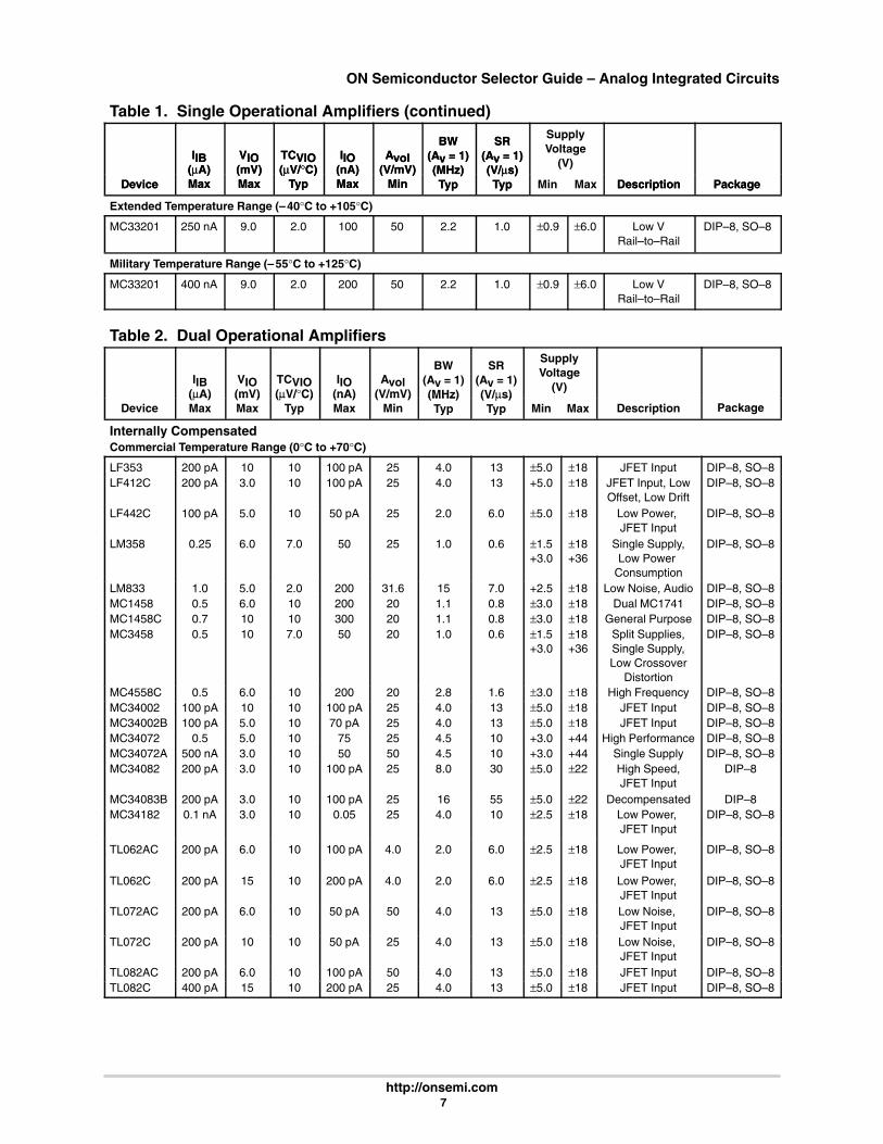
Table 1. Single Operational Amplifiers
IIB(µA)
VIO(mV)
TCVIO(µV/°C)
IIO(nA)
Avol(V/mV)
BW(Av = 1)(MHz)
SR(Av = 1)(V/µs)
SupplyVoltage
(V)
Device(µA)Max
(mV)Max
(µV/ C)Typ
(nA)Max
(V/mV)Min
(MHz)Typ
(V/µs)Typ Min Max Description Package
NoncompensatedCommercial Temperature Range (0°C to +70°C)
LM301A 0.25 7.5 10 50 25 1.0 0.5 ±3.0 ±18 GeneralPurpose
DIP–8, SO–8
LM308A 7.0 0.5 5.0 1.0 80 1.0 0.3 ±3.0 ±18 Precision DIP–8, SO–8
Industrial Temperature Range (–25°C to +85°C)
LM201A 0.075 2.0 10 10 50 1.0 0.5 ±3.0 ±22 GeneralPurpose
DIP–8, SO–8
Internally CompensatedCommercial Temperature Range (0°C to +70°C)
LF351 200 pA 10 10 100 pA 25 4.0 13 ±5.0 ±18 JFET Input DIP–8, SO–8LF411C 200 pA 2.0 10 100 pA 25 8.0 25 +5.0 ±22 JFET Input,
Low Offset,Low Drift
DIP–8, SO–8
MC1436, C 0.04 10 12 10 70 1.0 2.0 ±15 ±34 High Voltage DIP–8, SO–8MC1741C 0.5 6.0 15 200 20 1.0 0.5 ±3.0 ±18 General
PurposeDIP–8, SO–8
MC1776C 0.003 6.0 15 3.0 100 1.0 0.2 ±1.2 ±18 µPower,Programmable
DIP–8, SO–8
MC34001 200 pA 10 10 100 pA 25 4.0 13 ±5.0 ±18 JFET Input DIP–8, SO–8MC34071 0.5 5.0 10 75 25 4.5 10 +3.0 +44 High
PerformanceDIP–8, SO–8
MC34071A 500 nA 3.0 10 50 50 4.5 10 +3.0 +44 Single Supply DIP–8, SO–8MC34080B 200 pA 1.0 10 100 pA 25 16 55 ±5.0 ±22 Decompensated DIP–8, SO–8MC34081B 200 pA 1.0 10 100 pA 25 8.0 30 ±5.0 ±22 High Speed,
JFET InputDIP–8, SO–8
MC34181 0.1 nA 2.0 10 0.05 25 4.0 10 ±2.5 ±18 Low Power,JFET Input
DIP–8, SO–8
TL081AC 200 pA 6.0 10 100 pA 50 4.0 13 ±5.0 ±18 JFET Input DIP–8, SO–8TL081C 400 pA 15 10 200 pA 25 4.0 13 ±5.0 ±18 JFET Input DIP–8, SO–8
Automotive Temperature Range (–40°C to +85°C)
MC33071 0.5 5.0 10 75 25 4.5 10 +3.0 +44 HighPerformance
DIP–8, SO–8
MC33071A 500 nA 3.0 10 50 50 4.5 10 +3.0 +44 Single Supply DIP–8, SO–8MC33171 0.1 4.5 10 20 50 1.8 2.1 +3.0 +44 Low Power,
Single SupplyDIP–8, SO–8
MC33181 0.1 nA 2.0 10 0.05 25 4.0 10 ±2.5 ±18 Low Power,JFET Input
DIP–8, SO–8
ON Semiconductor Selector Guide – Analog Integrated Circuits
http://onsemi.com 7
Table 1. Single Operational Amplifiers (continued)
Device PackageDescription
SupplyVoltage
(V)
SR(Av = 1)(V/µs)Typ
BW(Av = 1)(MHz)Typ
Avol(V/mV)
Min
IIO(nA)Max
TCVIO(µV/°C)
Typ
VIO(mV)Max
IIB(µA)MaxDevice PackageDescriptionMaxMin
SR(Av = 1)(V/µs)Typ
BW(Av = 1)(MHz)Typ
Avol(V/mV)
Min
IIO(nA)Max
TCVIO(µV/°C)
Typ
VIO(mV)Max
IIB(µA)Max
Extended Temperature Range (–40°C to +105°C)
MC33201 250 nA 9.0 2.0 100 50 2.2 1.0 ±0.9 ±6.0 Low VRail–to–Rail
DIP–8, SO–8
Military Temperature Range (–55°C to +125°C)
MC33201 400 nA 9.0 2.0 200 50 2.2 1.0 ±0.9 ±6.0 Low VRail–to–Rail
DIP–8, SO–8
Table 2. Dual Operational Amplifiers
IIB(µA)
VIO(mV)
TCVIO(µV/°C)
IIO(nA)
Avol(V/mV)
BW(Av = 1)(MHz)
SR(Av = 1)(V/µs)
SupplyVoltage
(V)
Device(µA)Max
(mV)Max
(µV/ C)Typ
(nA)Max
(V/mV)Min
(MHz)Typ
(V/µs)Typ Min Max Description Package
Internally CompensatedCommercial Temperature Range (0°C to +70°C)
LF353 200 pA 10 10 100 pA 25 4.0 13 ±5.0 ±18 JFET Input DIP–8, SO–8LF412C 200 pA 3.0 10 100 pA 25 4.0 13 +5.0 ±18 JFET Input, Low
Offset, Low DriftDIP–8, SO–8
LF442C 100 pA 5.0 10 50 pA 25 2.0 6.0 ±5.0 ±18 Low Power, JFET Input
DIP–8, SO–8
LM358 0.25 6.0 7.0 50 25 1.0 0.6 ±1.5+3.0
±18+36
Single Supply,Low Power
Consumption
DIP–8, SO–8
LM833 1.0 5.0 2.0 200 31.6 15 7.0 +2.5 ±18 Low Noise, Audio DIP–8, SO–8MC1458 0.5 6.0 10 200 20 1.1 0.8 ±3.0 ±18 Dual MC1741 DIP–8, SO–8MC1458C 0.7 10 10 300 20 1.1 0.8 ±3.0 ±18 General Purpose DIP–8, SO–8MC3458 0.5 10 7.0 50 20 1.0 0.6 ±1.5
+3.0±18+36
Split Supplies,Single Supply,Low Crossover
Distortion
DIP–8, SO–8
MC4558C 0.5 6.0 10 200 20 2.8 1.6 ±3.0 ±18 High Frequency DIP–8, SO–8MC34002 100 pA 10 10 100 pA 25 4.0 13 ±5.0 ±18 JFET Input DIP–8, SO–8MC34002B 100 pA 5.0 10 70 pA 25 4.0 13 ±5.0 ±18 JFET Input DIP–8, SO–8MC34072 0.5 5.0 10 75 25 4.5 10 +3.0 +44 High Performance DIP–8, SO–8MC34072A 500 nA 3.0 10 50 50 4.5 10 +3.0 +44 Single Supply DIP–8, SO–8MC34082 200 pA 3.0 10 100 pA 25 8.0 30 ±5.0 ±22 High Speed,
JFET InputDIP–8
MC34083B 200 pA 3.0 10 100 pA 25 16 55 ±5.0 ±22 Decompensated DIP–8MC34182 0.1 nA 3.0 10 0.05 25 4.0 10 ±2.5 ±18 Low Power,
JFET InputDIP–8, SO–8
TL062AC 200 pA 6.0 10 100 pA 4.0 2.0 6.0 ±2.5 ±18 Low Power, JFET Input
DIP–8, SO–8
TL062C 200 pA 15 10 200 pA 4.0 2.0 6.0 ±2.5 ±18 Low Power, JFET Input
DIP–8, SO–8
TL072AC 200 pA 6.0 10 50 pA 50 4.0 13 ±5.0 ±18 Low Noise, JFET Input
DIP–8, SO–8
TL072C 200 pA 10 10 50 pA 25 4.0 13 ±5.0 ±18 Low Noise, JFET Input
DIP–8, SO–8
TL082AC 200 pA 6.0 10 100 pA 50 4.0 13 ±5.0 ±18 JFET Input DIP–8, SO–8TL082C 400 pA 15 10 200 pA 25 4.0 13 ±5.0 ±18 JFET Input DIP–8, SO–8
ON Semiconductor Selector Guide – Analog Integrated Circuits
http://onsemi.com 8
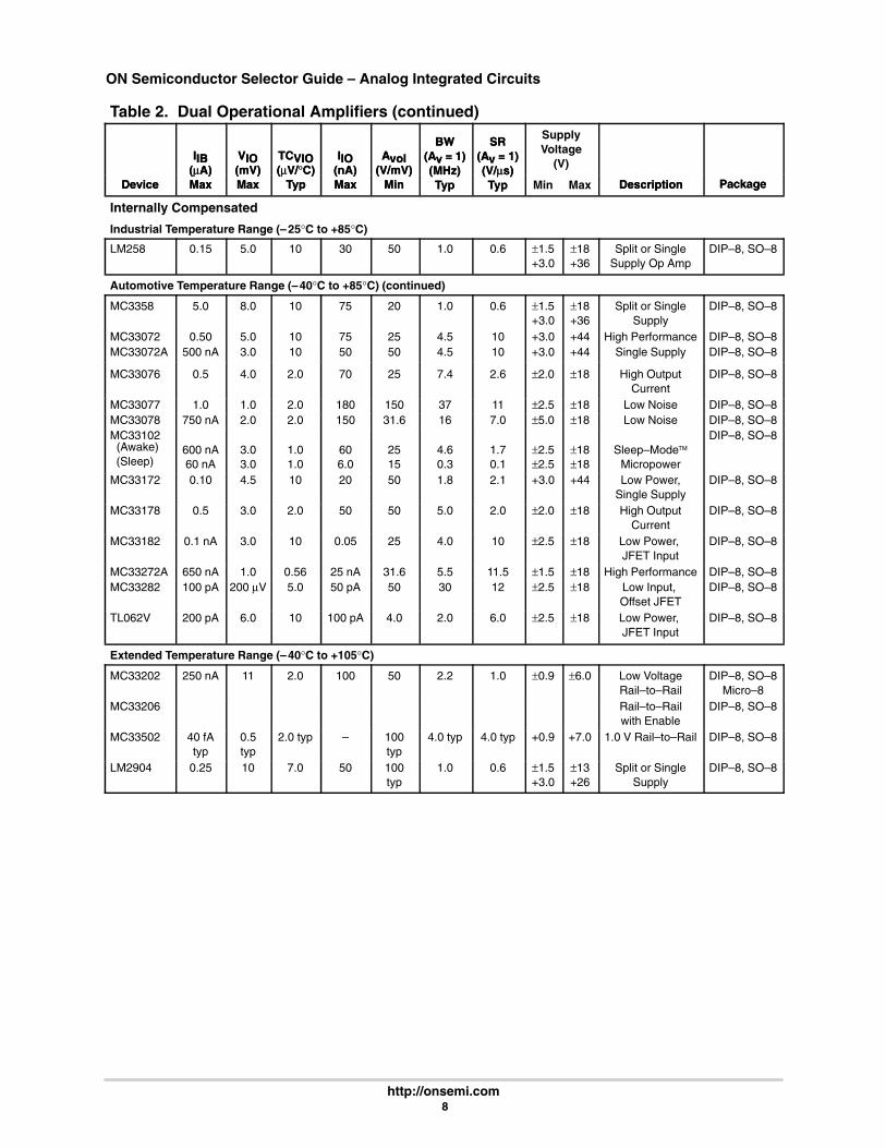
Table 2. Dual Operational Amplifiers (continued)
Device PackageDescription
SupplyVoltage
(V)
SR(Av = 1)(V/µs)Typ
BW(Av = 1)(MHz)Typ
Avol(V/mV)
Min
IIO(nA)Max
TCVIO(µV/°C)
Typ
VIO(mV)Max
IIB(µA)MaxDevice PackageDescriptionMaxMin
SR(Av = 1)(V/µs)Typ
BW(Av = 1)(MHz)Typ
Avol(V/mV)
Min
IIO(nA)Max
TCVIO(µV/°C)
Typ
VIO(mV)Max
IIB(µA)Max
Internally Compensated
Industrial Temperature Range (–25°C to +85°C)
LM258 0.15 5.0 10 30 50 1.0 0.6 ±1.5+3.0
±18+36
Split or SingleSupply Op Amp
DIP–8, SO–8
Automotive Temperature Range (–40°C to +85°C) (continued)
MC3358 5.0 8.0 10 75 20 1.0 0.6 ±1.5+3.0
±18+36
Split or SingleSupply
DIP–8, SO–8
MC33072 0.50 5.0 10 75 25 4.5 10 +3.0 +44 High Performance DIP–8, SO–8MC33072A 500 nA 3.0 10 50 50 4.5 10 +3.0 +44 Single Supply DIP–8, SO–8
MC33076 0.5 4.0 2.0 70 25 7.4 2.6 ±2.0 ±18 High OutputCurrent
DIP–8, SO–8
MC33077 1.0 1.0 2.0 180 150 37 11 ±2.5 ±18 Low Noise DIP–8, SO–8MC33078 750 nA 2.0 2.0 150 31.6 16 7.0 ±5.0 ±18 Low Noise DIP–8, SO–8MC33102 (Awake) (Sleep)
600 nA60 nA
3.03.0
1.01.0
606.0
2515
4.60.3
1.70.1
±2.5±2.5
±18±18
Sleep–ModeMicropower
DIP–8, SO–8
MC33172 0.10 4.5 10 20 50 1.8 2.1 +3.0 +44 Low Power,Single Supply
DIP–8, SO–8
MC33178 0.5 3.0 2.0 50 50 5.0 2.0 ±2.0 ±18 High OutputCurrent
DIP–8, SO–8
MC33182 0.1 nA 3.0 10 0.05 25 4.0 10 ±2.5 ±18 Low Power, JFET Input
DIP–8, SO–8
MC33272A 650 nA 1.0 0.56 25 nA 31.6 5.5 11.5 ±1.5 ±18 High Performance DIP–8, SO–8MC33282 100 pA 200 µV 5.0 50 pA 50 30 12 ±2.5 ±18 Low Input,
Offset JFETDIP–8, SO–8
TL062V 200 pA 6.0 10 100 pA 4.0 2.0 6.0 ±2.5 ±18 Low Power, JFET Input
DIP–8, SO–8
Extended Temperature Range (–40°C to +105°C)
MC33202 250 nA 11 2.0 100 50 2.2 1.0 ±0.9 ±6.0 Low VoltageRail–to–Rail
DIP–8, SO–8Micro–8
MC33206 Rail–to–Railwith Enable
DIP–8, SO–8
MC33502 40 fAtyp
0.5typ
2.0 typ – 100typ
4.0 typ 4.0 typ +0.9 +7.0 1.0 V Rail–to–Rail DIP–8, SO–8
LM2904 0.25 10 7.0 50 100typ
1.0 0.6 ±1.5+3.0
±13+26
Split or SingleSupply
DIP–8, SO–8
ON Semiconductor Selector Guide – Analog Integrated Circuits
http://onsemi.com 9
Table 2. Dual Operational Amplifiers (continued)
Device PackageDescription
SupplyVoltage
(V)
SR(Av = 1)(V/µs)Typ
BW(Av = 1)(MHz)Typ
Avol(V/mV)
Min
IIO(nA)Max
TCVIO(µV/°C)
Typ
VIO(mV)Max
IIB(µA)MaxDevice PackageDescriptionMaxMin
SR(Av = 1)(V/µs)Typ
BW(Av = 1)(MHz)Typ
Avol(V/mV)
Min
IIO(nA)Max
TCVIO(µV/°C)
Typ
VIO(mV)Max
IIB(µA)Max
Internally Compensated
Extended Automotive Temperature Range (–40°C to +125°C)
TCA0372 500 nA 15 20 50 30 1.1 1.4 +5.0 +36 Power Op Amp,Single Supply
DIP–8,DIP–16,SO–16L
LM2904V 0.25 13 7.0 50 100typ
1.0 0.6 ±1.5+3.0
±13+26
Split or SingleSupply
DIP–8, SO–8
Military Temperature Range (–55°C to +125°C)
MC33202 400 pA 11 2.0 200 pA 50 2.2 1.0 ±0.9 ±6.0 Low VRail–to–Rail
DIP–8, SO–8
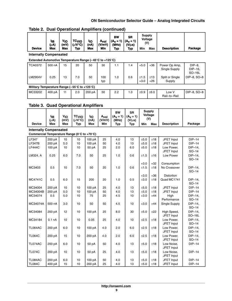
Table 3. Quad Operational Amplifiers
IIB(µA)
VIO(mV)
TCVIO(µV/°C)
IIO(nA)
Avol(V/mV)
BW(Av = 1)(MHz)
SR(Av = 1)(V/µs)
SupplyVoltage
(V)
Device(µ )Max
( )Max
(µ )Typ
( )Max
( )Min
(MHz)Typ
(V/µs)Typ Min Max Description Package
Internally CompensatedCommercial Temperature Range (0°C to +70°C)
LF347 200 pA 10 10 100 pA 25 4.0 13 ±5.0 ±18 JFET Input DIP–14LF347B 200 pA 5.0 10 100 pA 50 4.0 13 ±5.0 ±18 JFET Input DIP–14LF444C 100 pA 10 10 50 pA 25 2.0 6.0 ±5.0 ±18 Low Power,
JFET InputDIP–14,SO–14
LM324, A 0.25 6.0 7.0 50 25 1.0 0.6 ±1.5 ±16 Low Power DIP–14,SO–14
+3.0 +32 ConsumptionMC3403 0.5 10 7.0 50 20 1.0 0.6 ±1.5 ±18 No Crossover DIP–14,
SO–14+3.0 +36 Distortion
MC4741C 0.5 6.0 15 200 20 1.0 0.5 ±3.0 ±18 Quad MC1741 DIP–14,SO–14
MC34004 200 pA 10 10 100 pA 25 4.0 13 ±5.0 ±18 JFET Input DIP–14MC34004B 200 pA 5.0 10 100 pA 50 4.0 13 ±5.0 ±18 JFET Input DIP–14MC34074 0.5 5.0 10 75 25 4.5 10 +3.0 +44 High
PerformanceDIP–14,SO–14
MC34074A 500 nA 3.0 10 50 50 4.5 10 +3.0 +44 Single Supply DIP–14,SO–14
MC34084 200 pA 12 10 100 pA 25 8.0 30 ±5.0 ±22 High Speed,JFET Input
DIP–14,SO–16L
MC34184 0.1 nA 10 10 0.05 25 4.0 10 ±2.5 ±18 Low Power,JFET Input
DIP–14,SO–14
TL064AC 200 pA 6.0 10 100 pA 4.0 2.0 6.0 ±2.5 ±18 Low Power,JFET Input
DIP–14,SO–14
TL064C 200 pA 15 10 200 pA 4.0 2.0 6.0 ±2.5 ±18 Low Power,JFET Input
DIP–14,SO–14
TL074AC 200 pA 6.0 10 50 pA 50 4.0 13 ±5.0 ±18 Low Noise,JFET Input
DIP–14
TL074C 200 pA 10 10 50 pA 25 4.0 13 ±5.0 ±18 Low Noise,JFET Input
DIP–14
TL084AC 200 pA 6.0 10 100 pA 50 4.0 13 ±5.0 ±18 JFET Input DIP–14TL084C 400 pA 15 10 200 pA 25 4.0 13 ±5.0 ±18 JFET Input DIP–14
ON Semiconductor Selector Guide – Analog Integrated Circuits
http://onsemi.com 10
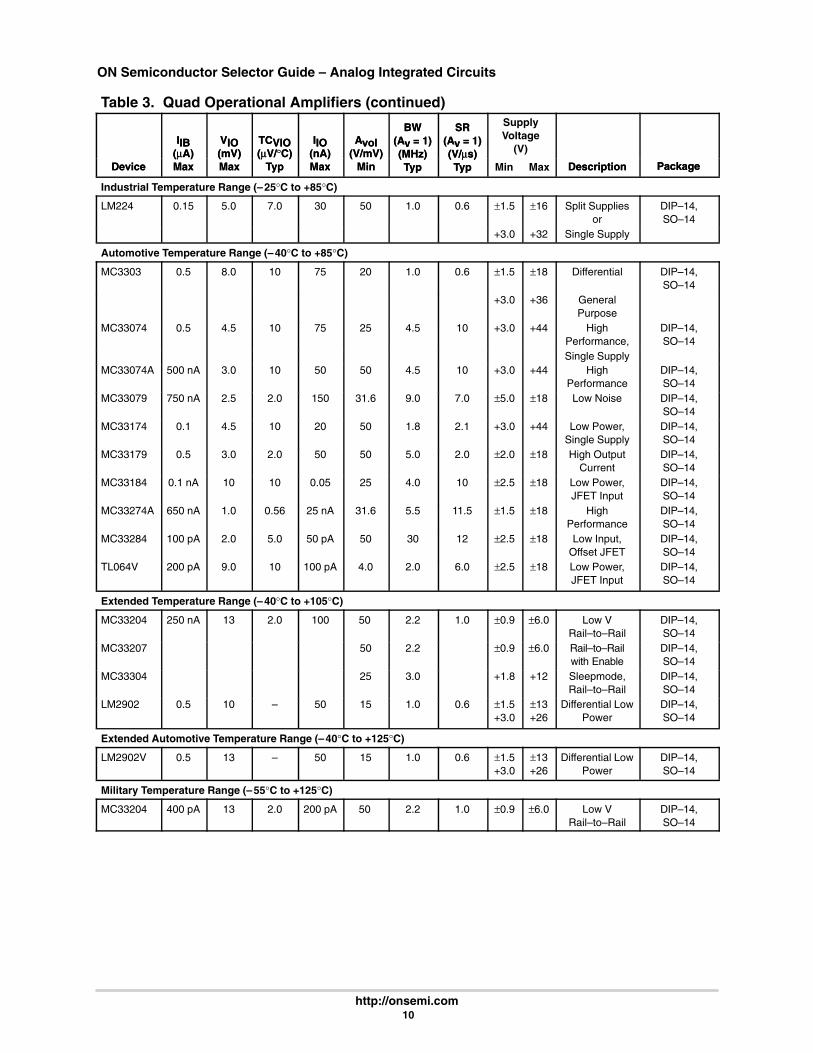
Table 3. Quad Operational Amplifiers (continued)
Device PackageDescription
SupplyVoltage
(V)
SR(Av = 1)(V/µs)Typ
BW(Av = 1)(MHz)Typ
Avol(V/mV)
Min
IIO(nA)Max
TCVIO(µV/°C)
Typ
VIO(mV)Max
IIB(µA)MaxDevice PackageDescriptionMaxMin
SR(Av = 1)(V/µs)Typ
BW(Av = 1)(MHz)Typ
Avol(V/mV)
Min
IIO(nA)Max
TCVIO(µV/°C)
Typ
VIO(mV)Max
IIB(µA)Max
Industrial Temperature Range (–25°C to +85°C)
LM224 0.15 5.0 7.0 30 50 1.0 0.6 ±1.5 ±16 Split Suppliesor
DIP–14,SO–14
+3.0 +32 Single Supply
Automotive Temperature Range (–40°C to +85°C)
MC3303 0.5 8.0 10 75 20 1.0 0.6 ±1.5 ±18 Differential DIP–14,SO–14
+3.0 +36 GeneralPurpose
MC33074 0.5 4.5 10 75 25 4.5 10 +3.0 +44 HighPerformance,
DIP–14,SO–14
Single SupplyMC33074A 500 nA 3.0 10 50 50 4.5 10 +3.0 +44 High
PerformanceDIP–14,SO–14
MC33079 750 nA 2.5 2.0 150 31.6 9.0 7.0 ±5.0 ±18 Low Noise DIP–14,SO–14
MC33174 0.1 4.5 10 20 50 1.8 2.1 +3.0 +44 Low Power,Single Supply
DIP–14,SO–14
MC33179 0.5 3.0 2.0 50 50 5.0 2.0 ±2.0 ±18 High OutputCurrent
DIP–14,SO–14
MC33184 0.1 nA 10 10 0.05 25 4.0 10 ±2.5 ±18 Low Power,JFET Input
DIP–14,SO–14
MC33274A 650 nA 1.0 0.56 25 nA 31.6 5.5 11.5 ±1.5 ±18 HighPerformance
DIP–14,SO–14
MC33284 100 pA 2.0 5.0 50 pA 50 30 12 ±2.5 ±18 Low Input,Offset JFET
DIP–14,SO–14
TL064V 200 pA 9.0 10 100 pA 4.0 2.0 6.0 ±2.5 ±18 Low Power,JFET Input
DIP–14,SO–14
Extended Temperature Range (–40°C to +105°C)
MC33204 250 nA 13 2.0 100 50 2.2 1.0 ±0.9 ±6.0 Low VRail–to–Rail
DIP–14,SO–14
MC33207 50 2.2 ±0.9 ±6.0 Rail–to–Railwith Enable
DIP–14,SO–14
MC33304 25 3.0 +1.8 +12 Sleepmode,Rail–to–Rail
DIP–14,SO–14
LM2902 0.5 10 – 50 15 1.0 0.6 ±1.5+3.0
±13+26
Differential LowPower
DIP–14,SO–14
Extended Automotive Temperature Range (–40°C to +125°C)
LM2902V 0.5 13 – 50 15 1.0 0.6 ±1.5+3.0
±13+26
Differential LowPower
DIP–14,SO–14
Military Temperature Range (–55°C to +125°C)
MC33204 400 pA 13 2.0 200 pA 50 2.2 1.0 ±0.9 ±6.0 Low VRail–to–Rail
DIP–14,SO–14

ON Semiconductor Selector Guide – Analog Integrated Circuits
http://onsemi.com 11
One Volt SMARTMOS Rail–to–RailDual Operational AmplifierMC33502D, P
TA = –40° to +105°C, DIP–8, SO–8 Packages
The MC33502 operational amplifier provides rail–to–rail operation on both the input and output. The outputcan swing within 50 mV of each rail. This rail–to–railoperation enables the user to make full use of the entiresupply voltage range available. It is designed to work atvery low supply voltages (1.0 V and ground), yet canoperate with a supply of up to 7.0 V and ground. Outputcurrent boosting techniques provide high output currentcapability while keeping the drain current of the ampli-fier to a minimum.• Low Voltage, Single Supply Operation (1.0 V and
Ground to 7.0 V and Ground)• High Input Impedance: Less than 40 fA Input
Current• Typical Unity Gain Bandwidth @ 5.0 V = 5.0 MHz,
@ 1.0 V = 4.0 MHz• High Output Current (ISC = 50 mA @ 5.0 V, 10 mA
@ 1.0 V)
• Output Voltage Swings within 50 mV of Both Rails• Input Voltage Range Includes Both Supply Rails• High Voltage Gain: 100 dB• No Phase Reversal on the Output for Over–Driven
Input Signals• Input Offset Trimmed to <500 µV Typical• Low Supply Current (ID = 1.2 mA, Typical)• 600 Ω Drive Capability• Extended Operating Temperature Range
(–40° to 105°C)
APPLICATIONS• Single Cell NiCd/Ni MH Powered Systems• Single Cell Lithium Powered Systems• Portable Communication Devices• Low Voltage Active Filters• General Systems Requiring Battery Power
Inputs InputStage Outputs
Buffer with 0 VLevel Shift
SaturationDetector
OffsetVoltage
Trim BaseCurrentBoost
BaseCurrentBoost
OutputStage
ON Semiconductor Selector Guide – Analog Integrated Circuits
http://onsemi.com 12
Miscellaneous AmplifiersON Semiconductor provides several Bipolar and CMOS
special purpose amplifiers which fill specific needs. Thesedevices range from low power CMOS programmable
amplifiers and comparators to variable–gain bipolar poweramplifiers.
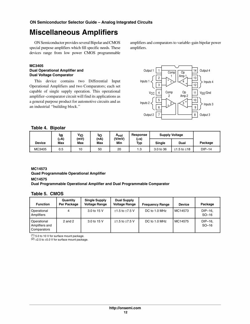
MC3405Dual Operational Amplifier andDual Voltage Comparator
This device contains two Differential InputOperational Amplifiers and two Comparators; each setcapable of single supply operation. This operationalamplifier–comparator circuit will find its applications asa general purpose product for automotive circuits and asan industrial ‘‘building block.’’
1
2
3
4
5
6
7 8
9
10
11
12
13
14Output 1
Inputs 1
VCC
Inputs 2
Output 2
VEE/Gnd
Output 4
Output 3
Inputs 4
Inputs 3
Comp1
OpAmp 1
Comp2
OpAmp 2
1
2 3
4++
++
Table 4. BipolarIIB
(µA)VIO(mV)
IIO(nA)
Avol(V/mV)
Response(µs)
Supply Voltage
Device(µA)Max
(mV)Max
(nA)Max
(V/mV)Min
(µs)Typ Single Dual Package
MC3405 0.5 10 50 20 1.3 3.0 to 36 ±1.5 to ±18 DIP–14
MC14573 Quad Programmable Operational Amplifier
MC14575 Dual Programmable Operational Amplifier and Dual Programmable Comparator
Table 5. CMOS
FunctionQuantity
Per PackageSingle SupplyVoltage Range
Dual SupplyVoltage Range Frequency Range Device Package
OperationalAmplifiers
4 3.0 to 15 V ±1.5 to ±7.5 V DC to 1.0 MHz MC14573 DIP–16,SO–16
OperationalAmplifiers andComparators
2 and 2 3.0 to 15 V ±1.5 to ±7.5 V DC to 1.0 MHz MC14575 DIP–16,SO–16
(1) 5.0 to 10 V for surface mount package.(2) ±2.5 to ±5.0 V for surface mount package.
ON Semiconductor Selector Guide – Analog Integrated Circuits
http://onsemi.com 13
ComparatorsTable 6. Single Comparators
IIB(µA)
VIO(mV)
IIO(µA)
AV(V/V)
IIO(mA)
ResponseTime
SupplyVoltage
TemperatureRange
Device(µA)Max
(mV)Max
(µA)Max
(V/V)Typ
(mA)Min
Time(ns)
Voltage(V) Description
Range(°C) Package
Bipolar
LM211 0.1 3.0 0.01 200 k 8.0 200 +15, –15 With strobe, will –25 to +85 SO–8LM311 0.25 7.5 0.05 operate from
single supply0 to +70 SO–8,
DIP–8
Table 7. Dual Comparators IIB
(µA)VIO(mV)
IIO(µA)
AV(V/V)
IIO(mA)
ResponseTime
SupplyVoltage
TemperatureRange
Device(µA)Max
(mV)Max
(µA)Max
(V/V)Typ
(mA)Min
Time(ns)
Voltage(V) Description
Range(°C) Package
Bipolar
LM393LM393ALM2903
0.25 5.02.07 0
0.05 200 k 6.0 130013001500
±1.5 to ±18or
3 0 to 36
Designed forsingle or splitsupply operation
0 to +700 to +7040 to +105
SO–8,DIP–8
LM2903LM2903V
7.07.0
15001500
3.0 to 36 supply operation,input commonmode includes
–40 to +105–40 to +125
ground (negativesupply)
MC3405 0.5 10 0.05 200 k 6.0 1300 ±1.5 to ±7.5or
3 0 to 15
This devicecontains 2 opamps and 2
0 to +70 DIP–14
3.0 to 15 am s and 2comparators in asingle package
CMOS
MC14575 0.001 30 0.0001 2.0 k 3.0 1000 ±1.5 to ±7.5or
3.0 to 15
This devicecontains 2 opamps and 2comparators in asingle package
–40 to +85 DIP–16,SO–16
Table 8. Quad Comparators IIB
(µA)VIO(mV)
IIO(µA)
AV(V/V)
IIO(mA)
ResponseTime
SupplyVoltage
TemperatureRange
Device(µA)Max
(mV)Max
(µA)Max
(V/V)Typ
(mA)Min
Time(ns)
Voltage(V) Description
Range(°C) Package
Bipolar
LM239 0.25 5.0 0.05 200 k 6.0 1300 ±1.5 to ±18 Designed for –25 to +85 DIP–14,LM239A 2.0 200 k or single or split
l i–25 to +85 SO–14
LM339 5.0 200 k 3.0 to 36 supply operation,i t
0 to +70LM339A 2.0 200 k input common
d i l d0 to +70
LM2901 7.0 100 k mode includesground (negative
–40 to +85LM2901V 7.0 100 k ground (negative
supply)–40 to +125
MC3302 0.5 20 0.5 100 k supply) –40 to +85 DIP–14,SO–14
CMOS
MC14574 0.001 30 0.0001 2.0 k 3.0 1000 ±1.5 to ±7.5or
3.0 to 15
Externallyprogrammablepower dissipationwith 1 or2 resistors
–40 to +85 DIP–16,SO–16

ANALOG INTEGRATED CIRCUITS
SIGNALCONDITIONING
BATTERYMANAGEMENT
POWERMANAGEMENT
SYSTEMMANAGEMENT
MOTORCONTROL INTERFACE OTHER
CIRCUITS
Op–Amps
Comparators
LithiumBattery
ProtectionICs
ChargeControllers
DC–DCConverters
with Inductor
Off–LineSMPS
Controllers
UndervoltageSupervisory
OvervoltageSupervisory
DataTransmission
DisplayDrivers
Timers
Linear Four–QuadrantMultiplier
Power FactorControllers
VoltageReferences
Linear VoltageRegulators
LDO LinearVoltage
Regulators
MOSFET/IGBT Drivers
DedicatedDrivers
Dedicated PowerMgmnt Controllers
DC MotorControl
ON Semiconductor Selector Guide – Analog Integrated Circuits
http://onsemi.com 14
Battery Management In Brief . . .
Battery management encompasses many functionsand features for power conversion in portable elec-tronics and ON Semiconductor offers charge controland battery pack protection IC’s for these criticalapplications.
Battery charging requires that both safety and perfor-mance issues be addressed. It is important to know whento start and stop the charging activity so the battery is notovercharged or subjected to conditions that might dam-age the battery or degrade its performance.
The charging IC maintains precise control of outputvoltage and current in order to prevent damage to thebattery. Instead of using a myriad of discrete devices,ON Semiconductor offers integrated charging IC solu-tions to close the voltage and current feedback loop cir-cuit that incorporates a voltage and current amplifier,level shifting circuitry, summing circuitry, and a refer-ence. ON Semiconductor’s charge controllers are tar-geted for Nickel–based batteries, NiCd and/or NiMH.
PageLithium Battery Protection ICs 15. . . . . . . . . . . . . . . . . . . Charge Controllers 18. . . . . . . . . . . . . . . . . . . . . . . . . . . .
Battery protection IC’s perform critical charge anddischarge control within the battery pack as well asovercurrent and undervoltage protection. When a bat-tery cell is either overcharged or overdischarged its per-formance can be degraded and, in the case of Li–Ioncells, the battery pack safety can be compromised.ON Semiconductor has patented a technique of balanc-ing the individual cell voltage to enhance battery packlife instead of managing the pack by the worst–case cell.Sleep or standby mode operation must also be kept to aminimum to reduce battery pack drain during operationor storage. Finally, short circuit protection is required ofthese IC’s and they must be able to handle “hard’’ or“soft’’ short situations equally well.
ON Semiconductor’s line of protection circuits isdesigned for lithium–based battery packs (Li–ion orLi–polymer) that contains one or two cells in series.

ON Semiconductor Selector Guide – Analog Integrated Circuits
http://onsemi.com 15
Lithium Battery Protection ICsLithium Battery Protection Circuit for One or Two Cell Battery PacksMC33347AD, ADTB
TA = –25° to +85°C, SO–16, TSSOP–16 Packages
The MC33347A is a monolithic lithium batteryprotection circuit that is designed to enhance the usefuloperating life of one or two cell rechargeable batterypacks. Cell protection features consist of independentlyprogrammable charge and discharge limits for bothvoltage and current with a delayed current shutdown,continuous cell voltage balancing with the choice ofon–chip or external balancing resistors, and a virtuallyzero current sleepmode state when the cells aredischarged. Additional features include an on–chipcharge pump for reduced MOSFET losses whilecharging or discharging a low cell voltage battery pack,and the programmability for one or two cell batterypack. This protection circuit requires a minimumnumber of external components and is targeted forinclusion within the battery pack. This MC33347A is
available in standard and low profile 16 lead surfacemount packages.• Independently Programmable Charge and
Discharge Limits for Both Voltage and Current• Charge and Discharge Current Limit Detection with
Delayed Shutdown• Continuous Cell Voltage Balancing• On–Chip or External Balancing Resistors• Virtually Zero Current Sleepmode State when Cells
are Discharged• Charge Pump for Reduced Losses with a Low Cell
Voltage Battery Pack• Programmable for One or Two Cell Applications• Minimum External Components for Inclusion
within the Battery Pack• Available in Low Profile Surface Mount Packages
DischargeGate Drive
Output
Cell Program/Test
VCC/OverchargeCurrent Limit
Typical Two Cell Smart Battery Pack
Discharge VoltageThreshold
Charge PumpOutput
15 ChargeGate Drive
Output
14 12 11 ChargeGate DriveCommon
109Current Sense
Common13
4
2
3
1
16
Balance 2
Balance 1
Ground
VCell 1
6
7
8
5
Charge VoltageThreshold
Cell VoltageReturn
Cell Voltage
MC33347A
VCell2/Discharge
Current Limit
ON Semiconductor Selector Guide – Analog Integrated Circuits
http://onsemi.com 16
Lithium Battery Protection ICs (continued)
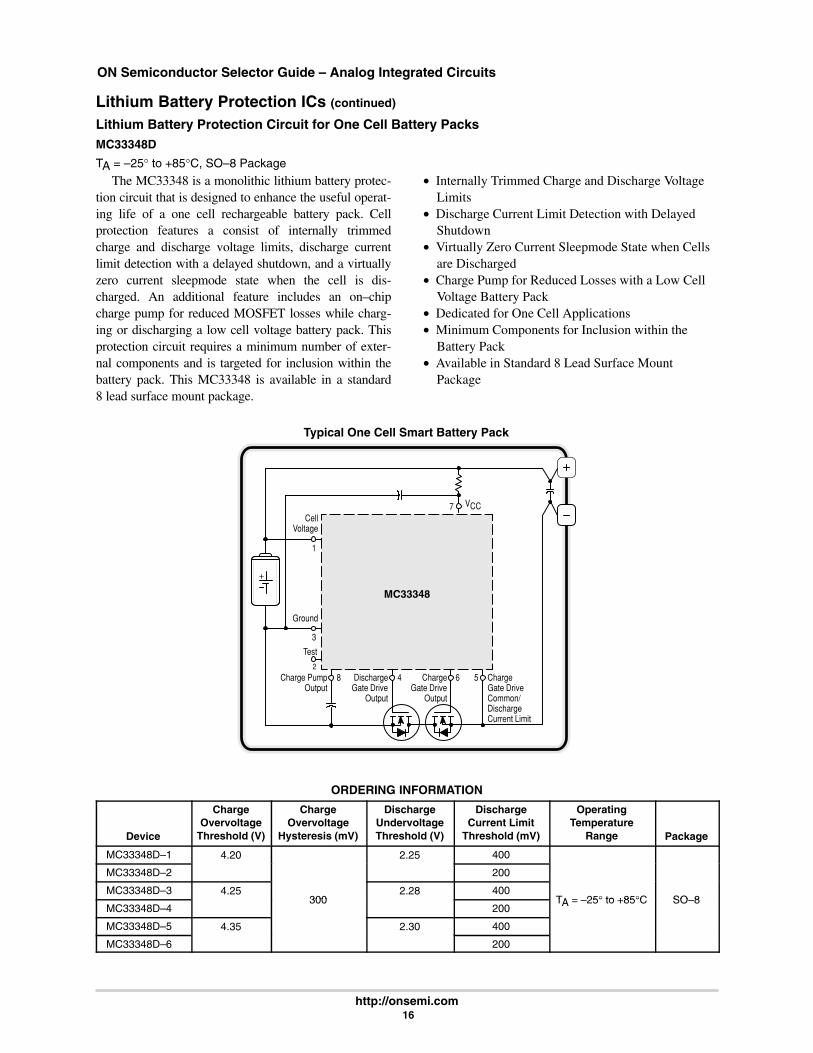
Lithium Battery Protection Circuit for One Cell Battery PacksMC33348D
TA = –25° to +85°C, SO–8 Package
The MC33348 is a monolithic lithium battery protec-tion circuit that is designed to enhance the useful operat-ing life of a one cell rechargeable battery pack. Cellprotection features a consist of internally trimmedcharge and discharge voltage limits, discharge currentlimit detection with a delayed shutdown, and a virtuallyzero current sleepmode state when the cell is dis-charged. An additional feature includes an on–chipcharge pump for reduced MOSFET losses while charg-ing or discharging a low cell voltage battery pack. Thisprotection circuit requires a minimum number of exter-nal components and is targeted for inclusion within thebattery pack. This MC33348 is available in a standard8 lead surface mount package.
• Internally Trimmed Charge and Discharge VoltageLimits
• Discharge Current Limit Detection with DelayedShutdown
• Virtually Zero Current Sleepmode State when Cellsare Discharged
• Charge Pump for Reduced Losses with a Low CellVoltage Battery Pack
• Dedicated for One Cell Applications• Minimum Components for Inclusion within the
Battery Pack• Available in Standard 8 Lead Surface Mount
Package
Typical One Cell Smart Battery Pack
VCC
Charge PumpOutput
8 ChargeGate Drive
Output
DischargeGate Drive
Output
4 6 5 ChargeGate DriveCommon/Discharge Current Limit
7
1
3
2
Ground
Test
MC33348
CellVoltage
ORDERING INFORMATION
Device
ChargeOvervoltage
Threshold (V)
ChargeOvervoltage
Hysteresis (mV)
DischargeUndervoltageThreshold (V)
DischargeCurrent Limit
Threshold (mV)
OperatingTemperature
Range Package
MC33348D–1 4.20 2.25 400
MC33348D–2 200
MC33348D–3 4.25300
2.28 400TA = 25° to +85°C SO 8
MC33348D–4300
200TA = –25° to +85°C SO–8
MC33348D–5 4.35 2.30 400
MC33348D–6 200

ON Semiconductor Selector Guide – Analog Integrated Circuits
http://onsemi.com 17
Lithium Battery Protection ICs (continued)
Lithium Battery Protection Circuit for One Cell Battery PacksMC33349TA = –40° to 85°C, SOT–23 6 Lead Package
The MC33349 is a monolithic lithium batteryprotection circuit that is designed to enhance the usefuloperating life of a one cell rechargeable battery pack.Cell protection features consist of internally trimmedcharge and discharge voltage limits, charge anddischarge current limit detection, and a virtually zerocurrent sleepmode state when the cell is discharged.This protection circuit requires a minimum number ofexternal components and is targeted for inclusion withinthe battery pack. This MC33349 is available in SOT–23
6 lead surface mount package.• Internally Trimmed Charge and Discharge Voltage
Limits• Charge and Discharge Current Limit Detection• Virtually Zero Current Sleepmode State when Cells
are Discharged• Dedicated for One Cell Applications• Minimum Components for Inclusion within the
Battery Pack• Available in a Low Profile Surface Mount Package
Typical One Cell Smart Battery Pack
This device contains 264 active transistors.
1 3 2
5
6
4
MC33349
0.1 µF
0.1 µF
0.01 µF
100 Ω
1.0 kΩ
ORDERING INFORMATION
Device
ChargeOvervoltage
Threshold (V)
ChargeOvervoltage
Hysteresis (mV)
DischargeUndervoltageThreshold (V)
Current LimitThreshold (mV)
OperatingTemperature
Range Package
MC33349N–3 4.25 200SOT 23
MC33349N–4 4.25 200 2.5 75 TA = –40° to 85°CSOT–23(6 Lead)
MC33349N–7 4.35 200(6 Lead)
ON Semiconductor Selector Guide – Analog Integrated Circuits
http://onsemi.com 18
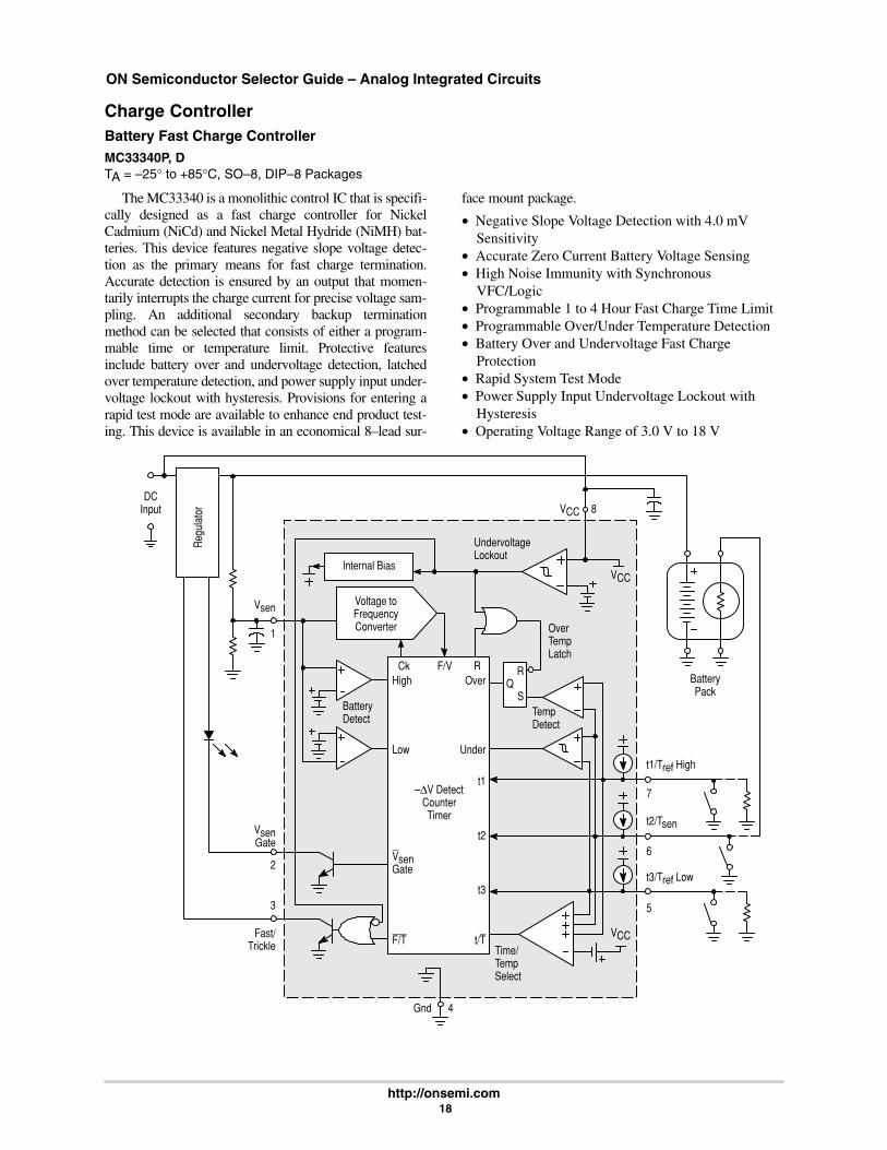
Charge ControllerBattery Fast Charge ControllerMC33340P, DTA = –25° to +85°C, SO–8, DIP–8 Packages
The MC33340 is a monolithic control IC that is specifi-cally designed as a fast charge controller for NickelCadmium (NiCd) and Nickel Metal Hydride (NiMH) bat-teries. This device features negative slope voltage detec-tion as the primary means for fast charge termination.Accurate detection is ensured by an output that momen-tarily interrupts the charge current for precise voltage sam-pling. An additional secondary backup terminationmethod can be selected that consists of either a program-mable time or temperature limit. Protective featuresinclude battery over and undervoltage detection, latchedover temperature detection, and power supply input under-voltage lockout with hysteresis. Provisions for entering arapid test mode are available to enhance end product test-ing. This device is available in an economical 8–lead sur-
face mount package.
• Negative Slope Voltage Detection with 4.0 mVSensitivity
• Accurate Zero Current Battery Voltage Sensing• High Noise Immunity with Synchronous
VFC/Logic• Programmable 1 to 4 Hour Fast Charge Time Limit• Programmable Over/Under Temperature Detection• Battery Over and Undervoltage Fast Charge
Protection• Rapid System Test Mode• Power Supply Input Undervoltage Lockout with
Hysteresis• Operating Voltage Range of 3.0 V to 18 V
BatteryDetect
DCInput VCC
UndervoltageLockout
OverTempLatch
TempDetect
Time/TempSelect
Vsen
VsenGate
Fast/Trickle
Voltage toFrequencyConverter
–∆V DetectCounterTimer
BatteryPack
Internal BiasVCC
VCC
Gnd
QR
S
t1/Tref High
t2/Tsen
t3/Tref Low
7
6
5
8
4
3
2
1
High
Low
VsenGate
F/T
Over
Under
t1
t2
t3
t/T
Ck F/V R
Reg
ulat
or
ON Semiconductor Selector Guide – Analog Integrated Circuits
http://onsemi.com 19
Charge Controller (continued)
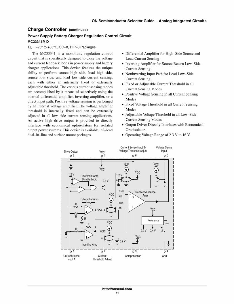
Power Supply Battery Charger Regulation Control CircuitMC33341P, D
TA = –25° to +85°C, SO–8, DIP–8 Packages
The MC33341 is a monolithic regulation controlcircuit that is specifically designed to close the voltageand current feedback loops in power supply and batterycharger applications. This device features the uniqueability to perform source high–side, load high–side,source low–side, and load low–side current sensing,each with either an internally fixed or externallyadjustable threshold. The various current sensing modesare accomplished by a means of selectively using theinternal differential amplifier, inverting amplifier, or adirect input path. Positive voltage sensing is performedby an internal voltage amplifier. The voltage amplifierthreshold is internally fixed and can be externallyadjusted in all low–side current sensing applications.An active high drive output is provided to directlyinterface with economical optoisolators for isolatedoutput power systems. This device is available in8–leaddual–in–line and surface mount packages.
• Differential Amplifier for High–Side Source andLoad Current Sensing
• Inverting Amplifier for Source Return Low–SideCurrent Sensing
• Noninverting Input Path for Load Low–SideCurrent Sensing
• Fixed or Adjustable Current Threshold in allCurrent Sensing Modes
• Positive Voltage Sensing in all Current SensingModes
• Fixed Voltage Threshold in all Current SensingModes
• Adjustable Voltage Threshold in all Low–SideCurrent Sensing Modes
• Output Driver Directly Interfaces with EconomicalOptoisolators
• Operating Voltage Range of 2.3 V to 16 V
4321
5678
GndCompensationCurrentThreshold Adjust
Current SenseInput A
Current Sense Input B/Voltage Threshold Adjust
Voltage SenseInputVCCDrive Output
Reference
Differential Amp
Inverting Amp
VCC
VCC
1.2 V
0.4 V
VCC
VCC
VCC
VCC
VCC
VCC
VCC
R
R
R
R
R
R
1.2 V
0.2 V 0.4 V 1.2 V
0.2 V
Differential AmpDisable Logic
TransconductanceAmp
VsenVth
IsenIth
V
I
ON Semiconductor Selector Guide – Analog Integrated Circuits
http://onsemi.com 20
Power Management Circuits
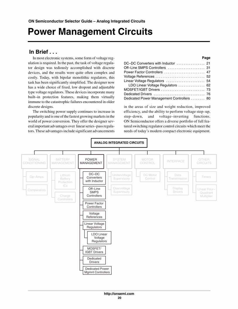
In Brief . . .In most electronic systems, some form of voltage reg-
ulation is required. In the past, the task of voltage regula-tor design was tediously accomplished with discretedevices, and the results were quite often complex andcostly. Today, with bipolar monolithic regulators, thistask has been significantly simplified. The designer nowhas a wide choice of fixed, low dropout and adjustabletype voltage regulators. These devices incorporate manybuilt–in protection features, making them virtuallyimmune to the catastrophic failures encountered in olderdiscrete designs.
The switching power supply continues to increase inpopularity and is one of the fastest growing markets in theworld of power conversion. They offer the designer sev-eral important advantages over linear series–pass regula-tors. These advantages include significant advancements
Page
DC–DC Converters with Inductor 21. . . . . . . . . . . . . . . . Off–Line SMPS Controllers 31. . . . . . . . . . . . . . . . . . . . . Power Factor Controllers 47. . . . . . . . . . . . . . . . . . . . . . . Voltage References 52. . . . . . . . . . . . . . . . . . . . . . . . . . . . Linear Voltage Regulators 54. . . . . . . . . . . . . . . . . . . . . .
LDO Linear Voltage Regulators 62. . . . . . . . . . . . . . . MOSFET/IGBT Drivers 73. . . . . . . . . . . . . . . . . . . . . . . . . Dedicated Drivers 76. . . . . . . . . . . . . . . . . . . . . . . . . . . . . Dedicated Power Management Controllers 80. . . . . . . .
in the areas of size and weight reduction, improvedefficiency, and the ability to perform voltage step–up,step–down, and voltage–inverting functions.ON Semiconductor offers a diverse portfolio of full fea-tured switching regulator control circuits which meet theneeds of today’s modern compact electronic equipment.
ANALOG INTEGRATED CIRCUITS
BATTERYMANAGEMENT
POWERMANAGEMENT
SYSTEMMANAGEMENT
MOTORCONTROL INTERFACE OTHER
CIRCUITS
LithiumBattery
ProtectionICs
ChargeControllers
DC–DCConverters
with Inductor
Off–LineSMPS
Controllers
UndervoltageSupervisory
OvervoltageSupervisory
DataTransmission
DisplayDrivers
Timers
Linear Four–QuadrantMultiplier
SIGNALCONDITIONING
Power FactorControllers
VoltageReferences
Linear VoltageRegulators
Op–Amps
LDO LinearVoltage
Regulators
Comparators
MOSFET/IGBT Drivers
DedicatedDrivers
Dedicated PowerMgmnt Controllers
DC MotorControl
ANALOG INTEGRATED CIRCUITS
SIGNALCONDITIONING
BATTERYMANAGEMENT
POWERMANAGEMENT
SYSTEMMANAGEMENT
MOTORCONTROL INTERFACE OTHER
CIRCUITS
Op–Amps
Comparators
LithiumBattery
ProtectionICs
ChargeControllers
DC–DCConverters
with Inductor
Off–LineSMPS
Controllers
UndervoltageSupervisory
OvervoltageSupervisory
DataTransmission
DisplayDrivers
Timers
Linear Four–QuadrantMultiplier
Power FactorControllers
VoltageReferences
Linear VoltageRegulators
LDO LinearVoltage
Regulators
MOSFET/IGBT Drivers
DedicatedDrivers
Dedicated PowerMgmnt Controllers
DC MotorControl
ON Semiconductor Selector Guide – Analog Integrated Circuits
http://onsemi.com 21
DC–DC Converters with Inductor
In Brief . . .Available in multiple DIP and surface mount pack-
ages, DC–DC converters from ON Semiconductor covera very wide range of output current levels from 50 mA upto 5 A and can be used in any topology, step–up, step–down, inverting and step–up and down.
These products are ideally suited to provide on–boardconversion in systems where the power is distributed tovarious elements or electronic boards.
Recent developments have used synchronous rectifi-cation and CMOS technology for better efficiency andlower current consumption.
Page
Single–Ended Controllers with On–ChipPower Switch 23. . . . . . . . . . . . . . . . . . . . . . . . . . . . . . . .
Easy Switcher Single–Ended Controllerswith On–Chip Power Switch 23. . . . . . . . . . . . . . . . . . . .
CMOS Micropower DC–to–DC Converters 25. . . . . . . . Synchronous Rectification DC/DC ConverterProgrammable Integrated Controller 27. . . . . . . . . . . . .
ON Semiconductor Selector Guide – Analog Integrated Circuits
http://onsemi.com 22
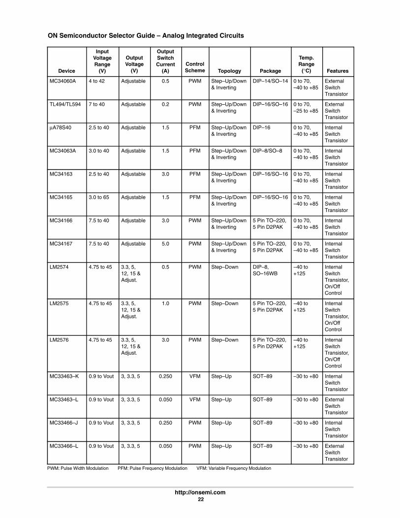
Device
InputVoltageRange
(V)
OutputVoltage
(V)
OutputSwitchCurrent
(A)ControlScheme Topology Package
Temp.Range
(°C) Features
MC34060A 4 to 42 Adjustable 0.5 PWM Step–Up/Down& Inverting
DIP–14/SO–14 0 to 70,–40 to +85
ExternalSwitchTransistor
TL494/TL594 7 to 40 Adjustable 0.2 PWM Step–Up/Down& Inverting
DIP–16/SO–16 0 to 70,–25 to +85
ExternalSwitchTransistor
µA78S40 2.5 to 40 Adjustable 1.5 PFM Step–Up/Down& Inverting
DIP–16 0 to 70,–40 to +85
InternalSwitchTransistor
MC34063A 3.0 to 40 Adjustable 1.5 PFM Step–Up/Down& Inverting
DIP–8/SO–8 0 to 70,–40 to +85
InternalSwitchTransistor
MC34163 2.5 to 40 Adjustable 3.0 PFM Step–Up/Down& Inverting
DIP–16/SO–16 0 to 70,–40 to +85
InternalSwitchTransistor
MC34165 3.0 to 65 Adjustable 1.5 PFM Step–Up/Down& Inverting
DIP–16/SO–16 0 to 70,–40 to +85
InternalSwitchTransistor
MC34166 7.5 to 40 Adjustable 3.0 PWM Step–Up/Down& Inverting
5 Pin TO–220,5 Pin D2PAK
0 to 70,–40 to +85
InternalSwitchTransistor
MC34167 7.5 to 40 Adjustable 5.0 PWM Step–Up/Down& Inverting
5 Pin TO–220,5 Pin D2PAK
0 to 70,–40 to +85
InternalSwitchTransistor
LM2574 4.75 to 45 3.3, 5,12, 15 &Adjust.
0.5 PWM Step–Down DIP–8,SO–16WB
–40 to+125
InternalSwitchTransistor,On/OffControl
LM2575 4.75 to 45 3.3, 5,12, 15 &Adjust.
1.0 PWM Step–Down 5 Pin TO–220,5 Pin D2PAK
–40 to+125
InternalSwitchTransistor,On/OffControl
LM2576 4.75 to 45 3.3, 5,12, 15 &Adjust.
3.0 PWM Step–Down 5 Pin TO–220,5 Pin D2PAK
–40 to+125
InternalSwitchTransistor,On/OffControl
MC33463–K 0.9 to Vout 3, 3.3, 5 0.250 VFM Step–Up SOT–89 –30 to +80 InternalSwitchTransistor
MC33463–L 0.9 to Vout 3, 3.3, 5 0.050 VFM Step–Up SOT–89 –30 to +80 ExternalSwitchTransistor
MC33466–J 0.9 to Vout 3, 3.3, 5 0.250 PWM Step–Up SOT–89 –30 to +80 InternalSwitchTransistor
MC33466–L 0.9 to Vout 3, 3.3, 5 0.050 PWM Step–Up SOT–89 –30 to +80 ExternalSwitchTransistor
PWM: Pulse Width Modulation PFM: Pulse Frequency Modulation VFM: Variable Frequency Modulation
ON Semiconductor Selector Guide – Analog Integrated Circuits
http://onsemi.com 23
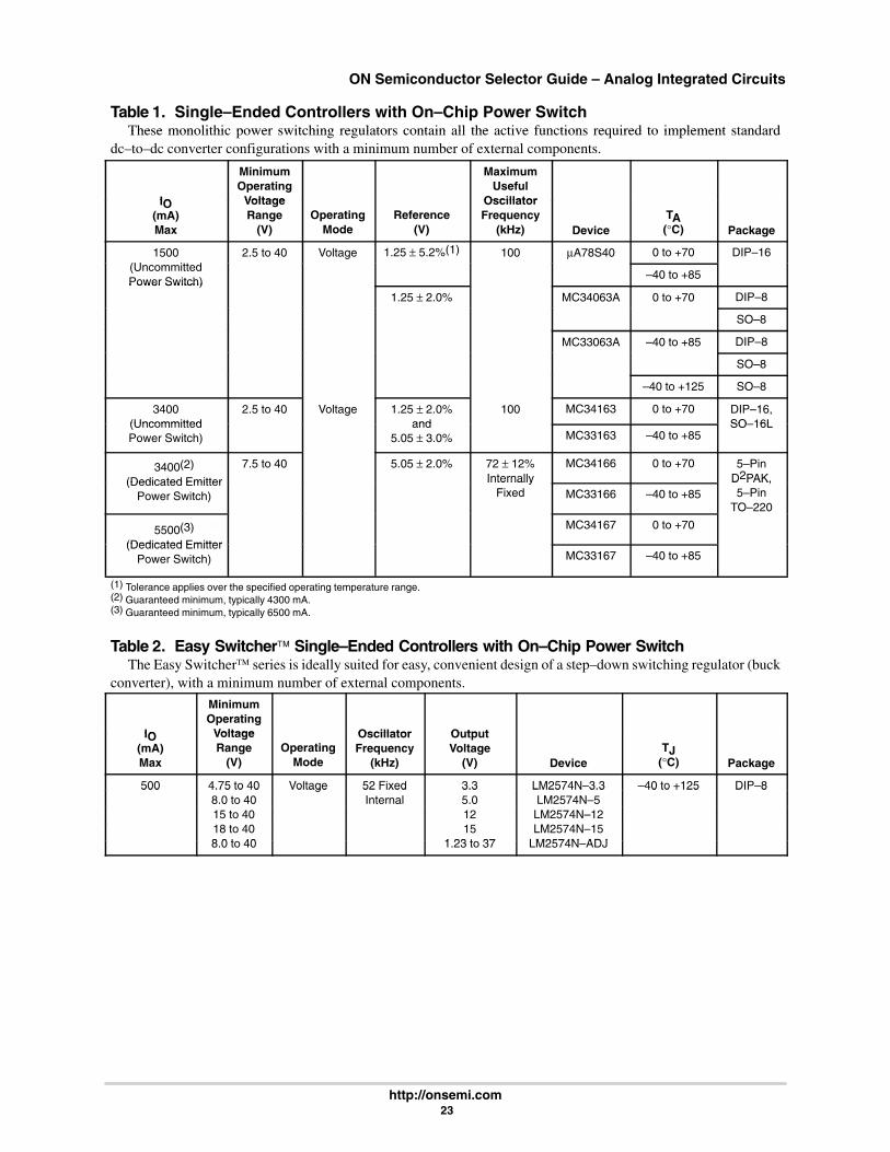
Table 1. Single–Ended Controllers with On–Chip Power Switch These monolithic power switching regulators contain all the active functions required to implement standardThese monolithic power switching regulators contain all the active functions required to implement standard
dc–to–dc converter configurations with a minimum number of external components.
IO
MinimumOperating
Voltage
MaximumUseful
OscillatorIO(mA)Max
VoltageRange
(V)Operating
ModeReference
(V)
OscillatorFrequency
(kHz) DeviceTA(°C) Package
1500(U i d
2.5 to 40 Voltage 1.25 ± 5.2%(1) 100 µA78S40 0 to +70 DIP–16(UncommittedPower Switch)
–40 to +85Power Switch)
1.25 ± 2.0% MC34063A 0 to +70 DIP–8
SO–8
MC33063A –40 to +85 DIP–8
SO–8
–40 to +125 SO–8
3400(Uncommitted
2.5 to 40 Voltage 1.25 ± 2.0%and
100 MC34163 0 to +70 DIP–16,SO 16L(Uncommitted
Power Switch)and
5.05 ± 3.0% MC33163 –40 to +85SO–16L
3400(2)
(Dedicated Emitter
7.5 to 40 5.05 ± 2.0% 72 ± 12%Internally
MC34166 0 to +70 5–PinD2PAK,(Dedicated Emitter
Power Switch)
InternallyFixed MC33166 –40 to +85
D PAK,5–Pin
TO–220
5500(3)
(Dedicated Emitter
MC34167 0 to +70
(Dedicated EmitterPower Switch) MC33167 –40 to +85
(1) Tolerance applies over the specified operating temperature range.(2) Guaranteed minimum, typically 4300 mA.(3) Guaranteed minimum, typically 6500 mA.
Table 2. Easy Switcher Single–Ended Controllers with On–Chip Power Switch The Easy Switcher series is ideally suited for easy, convenient design of a step–down switching regulator (buck
converter), with a minimum number of external components.
IO
MinimumOperating
Voltage Oscillator O tp tIO(mA)Max
VoltageRange
(V)Operating
Mode
OscillatorFrequency
(kHz)
OutputVoltage
(V) DeviceTJ
(°C) Package
500 4.75 to 40 Voltage 52 Fixed 3.3 LM2574N–3.3 –40 to +125 DIP–8500 4.75 to 408.0 to 40
Voltage 52 FixedInternal
3.35.0
LM2574N 3.3LM2574N–5
40 to +125 DIP 8
15 to 40 12 LM2574N–1218 to 408 0 t 40
151 23 t 37
LM2574N–15LM2574N ADJ8.0 to 40 1.23 to 37 LM2574N–ADJ
ON Semiconductor Selector Guide – Analog Integrated Circuits
http://onsemi.com 24
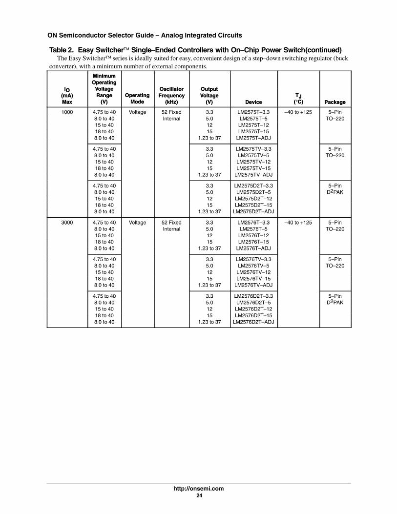
Table 2. Easy Switcher Single–Ended Controllers with On–Chip Power Switch(continued)The Easy Switcher series is ideally suited for easy, convenient design of a step–down switching regulator (buck
converter), with a minimum number of external components.
IO(mA)Max Package
TJ(°C)Device
OutputVoltage
(V)
OscillatorFrequency
(kHz)Operating
Mode
MinimumOperating
VoltageRange
(V)
IO(mA)Max Package
TJ(°C)Device
OutputVoltage
(V)
OscillatorFrequency
(kHz)Operating
Mode
MinimumOperating
VoltageRange
(V)
1000 4.75 to 40 Voltage 52 Fixed 3.3 LM2575T–3.3 –40 to +125 5–Pin1000 4.75 to 408.0 to 40
Voltage 52 FixedInternal
3.35.0
LM2575T 3.3LM2575T–5
40 to +125 5 PinTO–220
15 to 40 12 LM2575T–1218 to 408 0 t 40
151 23 t 37
LM2575T–15LM2575T ADJ8.0 to 40 1.23 to 37 LM2575T–ADJ
4.75 to 40 3.3 LM2575TV–3.3 5–Pin4.75 to 408.0 to 40
3.35.0
LM2575TV 3.3LM2575TV–5
5 PinTO–220
15 to 40 12 LM2575TV–1218 to 408 0 t 40
151 23 t 37
LM2575TV–15LM2575TV ADJ8.0 to 40 1.23 to 37 LM2575TV–ADJ
4.75 to 40 3.3 LM2575D2T–3.3 5–Pin4.75 to 408.0 to 40
3.35.0
LM2575D2T 3.3LM2575D2T–5
5 PinD2PAK
15 to 40 12 LM2575D2T–1218 to 408 0 t 40
151 23 t 37
LM2575D2T–15LM2575D2T ADJ8.0 to 40 1.23 to 37 LM2575D2T–ADJ
3000 4.75 to 40 Voltage 52 Fixed 3.3 LM2576T–3.3 –40 to +125 5–Pin3000 4.75 to 408.0 to 40
Voltage 52 FixedInternal
3.35.0
LM2576T 3.3LM2576T–5
40 to +125 5 PinTO–220
15 to 40 12 LM2576T–1218 to 408 0 t 40
151 23 t 37
LM2576T–15LM2576T ADJ8.0 to 40 1.23 to 37 LM2576T–ADJ
4.75 to 40 3.3 LM2576TV–3.3 5–Pin4.75 to 408.0 to 40
3.35.0
LM2576TV 3.3LM2576TV–5
5 PinTO–220
15 to 40 12 LM2576TV–1218 to 408 0 t 40
151 23 t 37
LM2576TV–15LM2576TV ADJ8.0 to 40 1.23 to 37 LM2576TV–ADJ
4.75 to 40 3.3 LM2576D2T–3.3 5–Pin4.75 to 408.0 to 40
3.35.0
LM2576D2T 3.3LM2576D2T–5
5 PinD2PAK
15 to 40 12 LM2576D2T–1218 to 408 0 t 40
151 23 t 37
LM2576D2T–15LM2576D2T ADJ8.0 to 40 1.23 to 37 LM2576D2T–ADJ
ON Semiconductor Selector Guide – Analog Integrated Circuits
http://onsemi.com 25
Switching Regulator Control Circuits (continued)
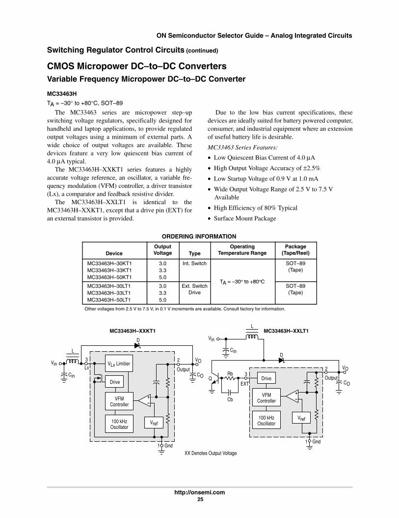
CMOS Micropower DC–to–DC ConvertersVariable Frequency Micropower DC–to–DC Converter
MC33463H
TA = –30° to +80°C, SOT–89
The MC33463 series are micropower step–upswitching voltage regulators, specifically designed forhandheld and laptop applications, to provide regulatedoutput voltages using a minimum of external parts. Awide choice of output voltages are available. Thesedevices feature a very low quiescent bias current of4.0 µA typical.
The MC33463H–XXKT1 series features a highlyaccurate voltage reference, an oscillator, a variable fre-quency modulation (VFM) controller, a driver transistor(Lx), a comparator and feedback resistive divider.
The MC33463H–XXLT1 is identical to theMC33463H–XXKT1, except that a drive pin (EXT) foran external transistor is provided.
Due to the low bias current specifications, thesedevices are ideally suited for battery powered computer,consumer, and industrial equipment where an extensionof useful battery life is desirable.
MC33463 Series Features:
• Low Quiescent Bias Current of 4.0 µA
• High Output Voltage Accuracy of ±2.5%
• Low Startup Voltage of 0.9 V at 1.0 mA
• Wide Output Voltage Range of 2.5 V to 7.5 VAvailable
• High Efficiency of 80% Typical
• Surface Mount Package
ORDERING INFORMATION
DeviceOutputVoltage Type
OperatingTemperature Range
Package(Tape/Reel)
MC33463H–30KT1 3.0 Int. Switch SOT–89MC33463H–33KT1 3.3 (Tape)MC33463H–50KT1 5.0
TA = 30° to +80°CMC33463H–30LT1 3.0 Ext. Switch
TA = –30° to +80°CSOT–89
MC33463H–33LT1 3.3 Drive (Tape)MC33463H–50LT1 5.0
Other voltages from 2.5 V to 7.5 V, in 0.1 V increments are available. Consult factory for information.
MC33463H–XXKT1 MC33463H–XXLT1
XX Denotes Output Voltage
Lx
D
Vin VLx Limitier3
Vref
Gnd
VFMController
100 kHzOscillator
2
Output
VO
CO Drive
VFMController
100 kHzOscillator
Vref
D
Vin
Output
VO
CO
Gnd1
3
EXT
L
QRb
Cb
1
2
Drive
L
Cin
Cin
ON Semiconductor Selector Guide – Analog Integrated Circuits
http://onsemi.com 26
CMOS Micropower DC–to–DC Converters (continued)
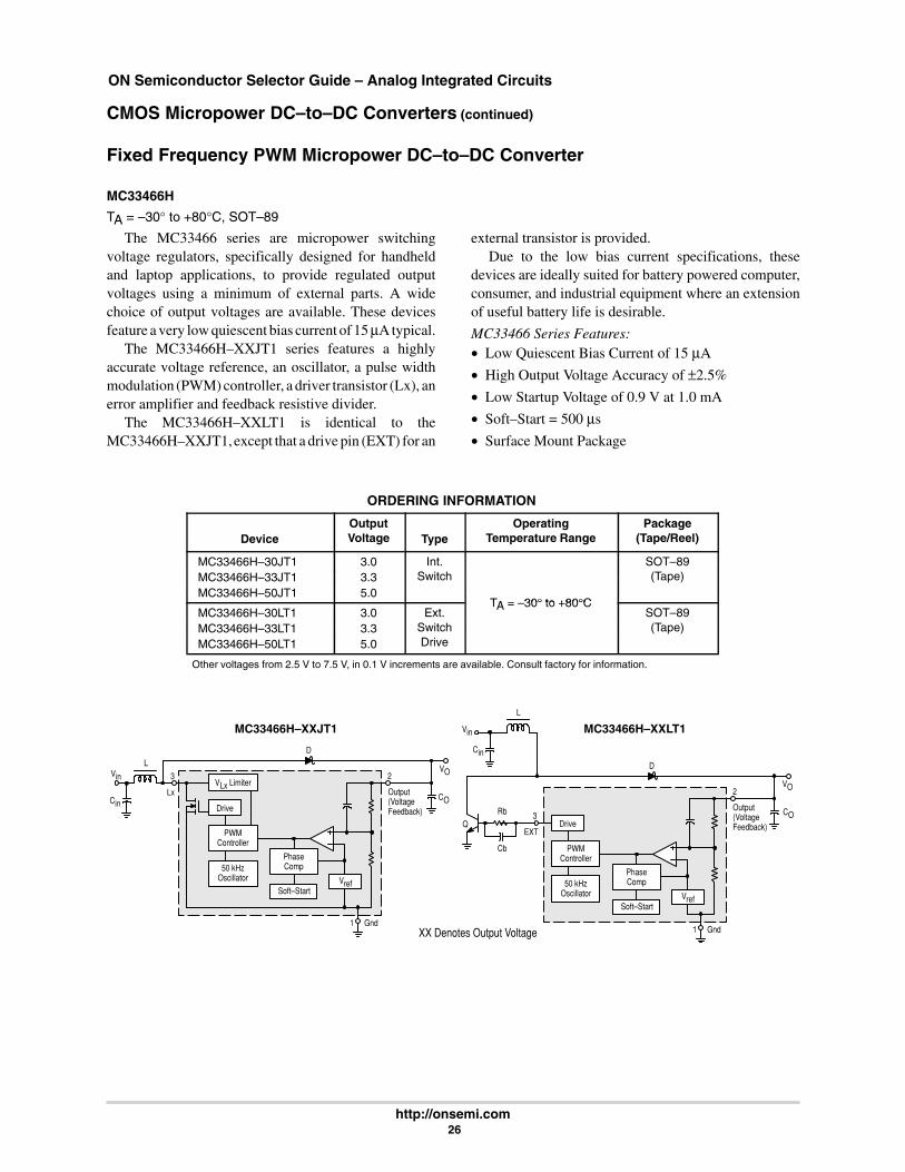
Fixed Frequency PWM Micropower DC–to–DC Converter
MC33466H
TA = –30° to +80°C, SOT–89
The MC33466 series are micropower switchingvoltage regulators, specifically designed for handheldand laptop applications, to provide regulated outputvoltages using a minimum of external parts. A widechoice of output voltages are available. These devicesfeature a very low quiescent bias current of 15 µA typical.
The MC33466H–XXJT1 series features a highlyaccurate voltage reference, an oscillator, a pulse widthmodulation (PWM) controller, a driver transistor (Lx), anerror amplifier and feedback resistive divider.
The MC33466H–XXLT1 is identical to theMC33466H–XXJT1, except that a drive pin (EXT) for an
external transistor is provided.Due to the low bias current specifications, these
devices are ideally suited for battery powered computer,consumer, and industrial equipment where an extensionof useful battery life is desirable.
MC33466 Series Features:• Low Quiescent Bias Current of 15 µA
• High Output Voltage Accuracy of ±2.5%
• Low Startup Voltage of 0.9 V at 1.0 mA
• Soft–Start = 500 µs
• Surface Mount Package
ORDERING INFORMATION
DeviceOutputVoltage Type
OperatingTemperature Range
Package(Tape/Reel)
MC33466H–30JT1 3.0 Int. SOT–89MC33466H–33JT1 3.3 Switch (Tape)MC33466H–50JT1 5.0
TA = 30° to +80°CMC33466H–30LT1 3.0 Ext.
TA = –30° to +80°CSOT–89
MC33466H–33LT1 3.3 SwitchD i
(Tape)MC33466H–50LT1 5.0 Drive
Other voltages from 2.5 V to 7.5 V, in 0.1 V increments are available. Consult factory for information.
Gnd
Drive
PWMController
50 kHzOscillator Vref
1
2VO
MC33466H–XXJT1 MC33466H–XXLT1
PhaseComp
Soft–Start
Output(VoltageFeedback)
3
EXT
Gnd
Drive
PWMController
50 kHzOscillator Vref
1
2VO
PhaseComp
Soft–Start
Output(VoltageFeedback)
3VLx Limiter
Lx
Vin
Vin
XX Denotes Output Voltage
COCO
D
D
L
L
Rb
Cb
Q
Cin
Cin
ON Semiconductor Selector Guide – Analog Integrated Circuits
http://onsemi.com 27
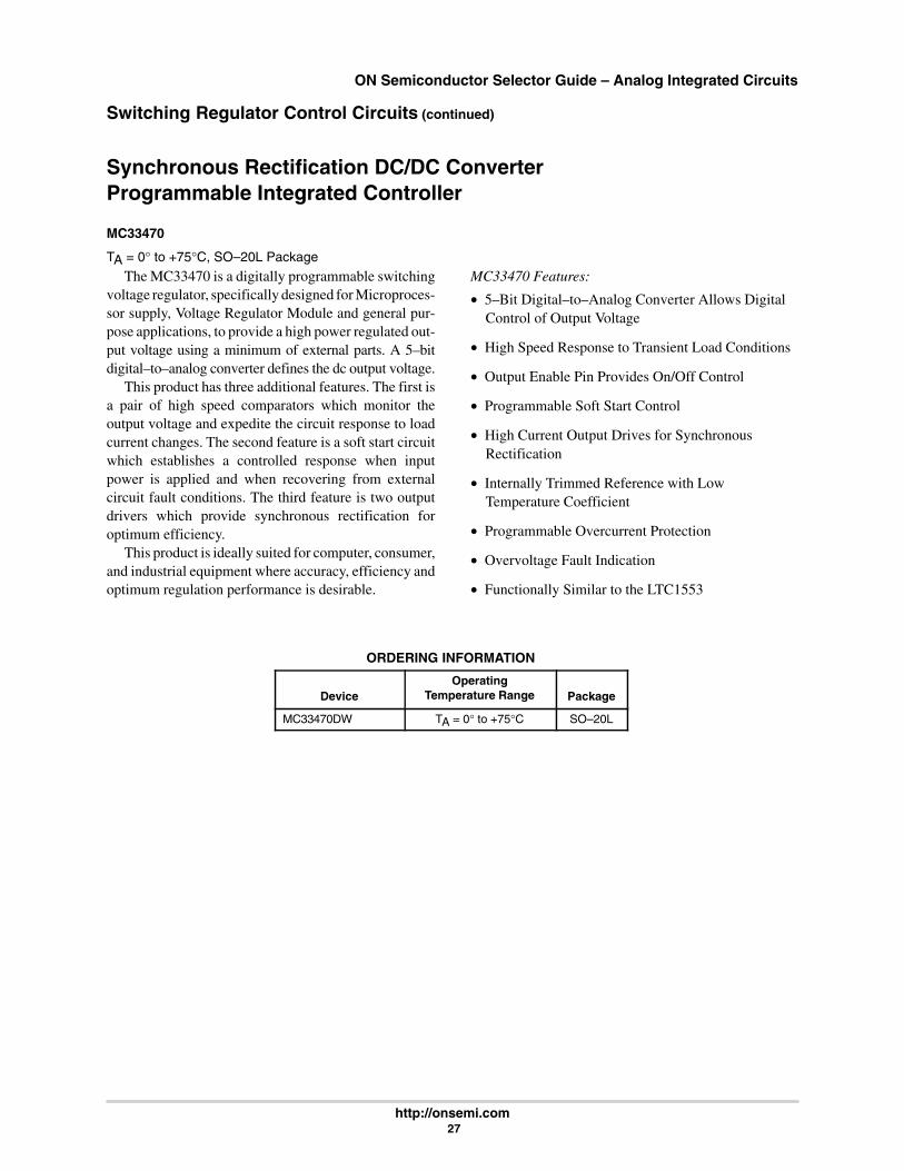
Switching Regulator Control Circuits (continued)
Synchronous Rectification DC/DC ConverterProgrammable Integrated Controller
MC33470
TA = 0° to +75°C, SO–20L Package
The MC33470 is a digitally programmable switchingvoltage regulator, specifically designed for Microproces-sor supply, Voltage Regulator Module and general pur-pose applications, to provide a high power regulated out-put voltage using a minimum of external parts. A 5–bitdigital–to–analog converter defines the dc output voltage.
This product has three additional features. The first isa pair of high speed comparators which monitor theoutput voltage and expedite the circuit response to loadcurrent changes. The second feature is a soft start circuitwhich establishes a controlled response when inputpower is applied and when recovering from externalcircuit fault conditions. The third feature is two outputdrivers which provide synchronous rectification foroptimum efficiency.
This product is ideally suited for computer, consumer,and industrial equipment where accuracy, efficiency andoptimum regulation performance is desirable.
MC33470 Features:
• 5–Bit Digital–to–Analog Converter Allows DigitalControl of Output Voltage
• High Speed Response to Transient Load Conditions
• Output Enable Pin Provides On/Off Control
• Programmable Soft Start Control
• High Current Output Drives for SynchronousRectification
• Internally Trimmed Reference with LowTemperature Coefficient
• Programmable Overcurrent Protection
• Overvoltage Fault Indication
• Functionally Similar to the LTC1553
ORDERING INFORMATION
DeviceOperating
Temperature Range Package
MC33470DW TA = 0° to +75°C SO–20L

ON Semiconductor Selector Guide – Analog Integrated Circuits
http://onsemi.com 28
Oscillator
PWMComparator
OTA Error Amp
VCC
Sense
Compensation
PGnd
G1
G2
Ifb
Over CurrentDetect
Outen
PowerGood
VID0
VID1
VID2
VID3
Vref
VCC
VoltageIdentification
CodeInput
Digitally ProgrammedReference
VCC
Vref
R
SQ
PWMLatch
+0.96 Vref
1.04 Vref
5
VID4
18
17
16
15
14
4 10
9
14
3
1
8
20
2
19
0.93 Vref
1.04 Vref13
AGnd
6
SS
800 µ
OverTemp
11
Imax
7
10 µA
2.5 V
1.5 V En
90 µA190 µA
S
RQ
Delay Fault1.14 Vref
20 µA
OT
Q
+
+
+
Delay
Simplified Block Diagram
PVCC

ON Semiconductor Selector Guide – Analog Integrated Circuits
http://onsemi.com 29
Switching Regulator Control Circuits (continued)
Easy Switcher Single–Ended Controllers with On–Chip Power SwitchStep–Down Voltage RegulatorsLM2574N–XX
TJ = –40° to +125°C, DIP–8
The LM2574 series of regulators are monolithicintegrated circuits ideally suited for easy and convenientdesign of a step–down switching regulator (buckconverter). All circuits of this series are capable of drivinga 0.5 A load with excellent line and load regulation. Thesedevices are available in fixed output voltages of 3.3 V, 5.0V, 12 V, 15 V, and an adjustable output version.
These regulators were designed to minimize thenumber of external components to simplify the powersupply design. Standard series of inductors optimized foruse with the LM2574 are offered by several differentinductor manufacturers.
Since the LM2574 converter is a switch–mode powersupply, its efficiency is significantly higher in comparisonwith popular three–terminal linear regulators, especiallywith higher input voltages. In most cases, the power dissi-pated by the LM2574 regulator is so low, that the coppertraces on the printed circuit board are normally the onlyheatsink needed and no additional heatsinking is required.
The LM2574 features include a guaranteed ±4%tolerance on output voltage within specified inputvoltages and output load conditions, and ±10% on theoscillator frequency (±2% over 0°C to +125°C). Externalshutdown is included, featuring 60 µA (typical) standbycurrent. The output switch includes cycle–by–cycle
current limiting, as well as thermal shutdown for fullprotection under fault conditions.Features• 3.3 V, 5.0 V, 12 V, 15 V, and Adjustable Output
Versions• Adjustable Version Output Voltage Range, 1.23 to
37 V ±4% max over Line and Load Conditions• Guaranteed 0.5 A Output Current• Wide Input Voltage Range: 4.75 to 40 V• Requires Only 4 External Components• 52 kHz Fixed Frequency Internal Oscillator• TTL Shutdown Capability, Low Power Standby
Mode• High Efficiency• Uses Readily Available Standard Inductors• Thermal Shutdown and Current Limit ProtectionApplications• Simple and High–Efficiency Step–Down (Buck)
Regulators• Efficient Pre–Regulator for Linear Regulators• On–Card Switching Regulators• Positive to Negative Converters (Buck–Boost)• Negative Step–Up Converters• Power Supply for Battery ChargersXX = Voltage Option, i.e., 3.3, 5, 12, 15 V; and ADJfor Adjustable Output
Representative Block Diagram and Typical Application
UnregulatedDC Input +Vin
5
Cout
Feedback
1
Cin
L1
D1
R2
R11.0 k
Output
7Pwr Gnd
4
ON/OFF
3
Reset
Latch
ThermalShutdown
52 kHzOscillator
1.235 VBand–GapReference
FreqShift
18 kHz
ComparatorFixed GainError Amplifier
CurrentLimit
Driver
1.0 AmpSwitch
ON/OFF3.1 V Internal
Regulator
Vout
Load
OutputVoltage Versions
3.3 V5.0 V12 V15 V
R2(Ω)
1.7 k3.1 k8.84 k11.3 k
For adjustable versionR1 = open, R2 = 0 Ω
Sig Gnd
2

ON Semiconductor Selector Guide – Analog Integrated Circuits
http://onsemi.com 30
Step–Down Voltage Regulators (continued)
LM2575T–XX, TV, D2T, LM2576T–XX, TV, D2T
TJ = –40° to +125°C, TO–220 5 Leads, D2PAK 5 Leads
The LM2575/6 series of regulators are monolithic in-tegrated circuits ideally suited for easy and convenientdesign of a step–down switching regulator (buck con-verter). All circuits of this series are capable of driving a1.0 A (LM2575) or 3.0 A (LM2576) load with excellentline and load regulation. These devices are available infixed output voltages of 3.3 V, 5.0 V, 12 V, 15 V, and anadjustable output version.
These regulators were designed to minimize thenumber of external components to simplify the powersupply design. Standard series of inductors optimised foruse with the LM2575/6 are offered by several differentinductor manufacturers.
Since the LM2575/6 converter is a switch–mode powersupply, its efficiency is significantly higher in comparisonwith popular three–terminal linear regulators, especiallywith higher input voltages. In many cases, the powerdissipated by the LM2575/6 regulator is so low, that noheatsink is required or its size could be reduceddramatically.
The LM2575/6 features include a guaranteed ±4% toler-ance on output voltage within specified input voltages andoutput load conditions, and ±10% on the oscillator frequen-cy (±2% over 0°C to 125°C). External shutdown is in-cluded, featuring 80 µA typical standby current. The outputswitch includes cycle–by–cycle current limiting, as well asthermal shutdown for full protection under fault conditions.
Features• 3.3 V, 5.0 V, 12 V, 15 V, and Adjustable Output
Versions• Adjustable Version Output Voltage Range of 1.23 V
to 37 V ±4% Maximum Over Line and LoadConditions
• Guaranteed 1.0 A (LM2575) 3.0 A (LM2576)Output Current
• Wide Input Voltage Range: 4.75 V to 40 V• Requires Only 4 External Components• 52 kHz Fixed Frequency Internal Oscillator• TTL Shutdown Capability, Low Power Standby
Mode• High Efficiency• Uses Readily Available Standard Inductors• Thermal Shutdown and Current Limit Protection
Applications• Simple and High–Efficiency Step–Down (Buck)
Regulators• Efficient Pre–Regulator for Linear Regulators• On–Card Switching Regulators• Positive to Negative Converters (Buck–Boost)• Negative Step–Up Converters• Power Supply for Battery ChargersXX = Voltage Option, i.e., 3.3, 5, 12, 15 V; and ADJfor Adjustable Output
Representative Block Diagram and Typical Application
UnregulatedDC Input +Vin
1
Cout
Feedback
4
Cin
L1
D1
R2
R11.0 k
Output
2Gnd
3
ON/OFF
5
Reset
Latch
ThermalShutdown
52 kHzOscillator
1.235 VBand–GapReference
FreqShift
18 kHz
ComparatorFixed GainError Amplifier
CurrentLimit
Driver
1.0 AmpSwitch
ON/OFF3.1 V Internal
Regulator
RegulatedOutputVout
Load
OutputVoltage Versions
3.3 V5.0 V12 V15 V
R2(Ω)
1.7 k3.1 k8.84 k11.3 k
For adjustable versionR1 = open, R2 = 0 Ω
This device contains 162 active transistors.
ANALOG INTEGRATED CIRCUITS
SIGNALCONDITIONING
BATTERYMANAGEMENT
POWERMANAGEMENT
SYSTEMMANAGEMENT
MOTORCONTROL INTERFACE OTHER
CIRCUITS
Op–Amps
Comparators
LithiumBattery
ProtectionICs
ChargeControllers
DC–DCConverters
with Inductor
Off–LineSMPS
Controllers
UndervoltageSupervisory
OvervoltageSupervisory
DataTransmission
DisplayDrivers
Timers
Linear Four–QuadrantMultiplier
Power FactorControllers
VoltageReferences
Linear VoltageRegulators
LDO LinearVoltage
Regulators
MOSFET/IGBT Drivers
DedicatedDrivers
Dedicated PowerMgmnt Controllers
DC MotorControl
ON Semiconductor Selector Guide – Analog Integrated Circuits
http://onsemi.com 31
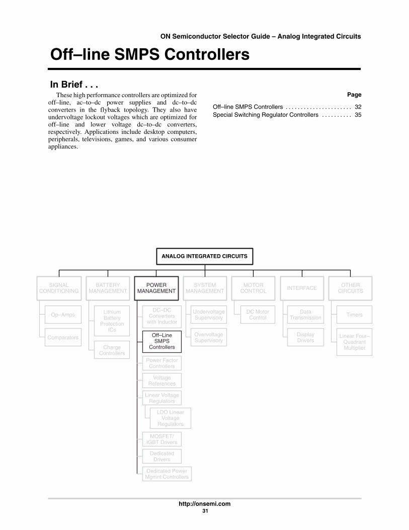
Off–line SMPS Controllers
In Brief . . .These high performance controllers are optimized for
off–line, ac–to–dc power supplies and dc–to–dcconverters in the flyback topology. They also haveundervoltage lockout voltages which are optimized foroff–line and lower voltage dc–to–dc converters,respectively. Applications include desktop computers,peripherals, televisions, games, and various consumerappliances.
Page
Off–line SMPS Controllers 32. . . . . . . . . . . . . . . . . . . . . . Special Switching Regulator Controllers 35. . . . . . . . . .
ON Semiconductor Selector Guide – Analog Integrated Circuits
http://onsemi.com 32
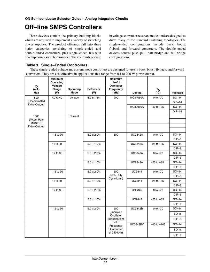
Off–line SMPS ControllersThese devices contain the primary building blocks
which are required to implement a variety of switchingpower supplies. The product offerings fall into threemajor categories consisting of single–ended anddouble–ended controllers, plus single–ended ICs withon–chip power switch transistors. These circuits operate
in voltage, current or resonant modes and are designed todrive many of the standard switching topologies. Thesingle–ended configurations include buck, boost,flyback and forward converters. The double–endeddevices control push–pull, half bridge and full bridgeconfigurations.
Table 3. Single–Ended Controllers These single–ended voltage and current mode controllers are designed for use in buck, boost, flyback, and forward
converters. They are cost effective in applications that range from 0.1 to 200 W power output.
IO
MinimumOperating
Voltage
MaximumUseful
OscillatorIO(mA)Max
VoltageRange
(V)Operating
ModeReference
(V)
OscillatorFrequency
(kHz) DeviceTA(°C) Package
500 7.0 to 40 Voltage 5.0 ± 1.5% 200 MC34060A 0 to +70 SO–14(UncommittedDrive Output)
DIP–14Drive Output)
MC33060A –40 to +85 SO–14
DIP–14
1000 Current(Totem Pole
MOSFETMOSFETDrive Output)Drive Out ut)
11.5 to 30 5.0 ± 2.0% 500 UC3842A 0 to +70 SO–14
DIP–8
11 to 30 5.0 ± 1.0% UC2842A –25 to +85 SO–14
DIP–8
8.2 to 30 5.0 ± 2.0% UC3843A 0 to +70 SO–14
DIP–8
5.0 ± 1.0% UC2843A –25 to +85 SO–14
DIP–8
11.5 to 30 5.0 ± 2.0% 500 UC3844 0 to +70 SO–14(50% DutyCycle Limit)
DIP–8
11 to 30 5.0 ± 1.0%Cycle Limit)
UC2844 –25 to +85 SO–14
DIP–8
8.2 to 30 5.0 ± 2.0% UC3845 0 to +70 SO–14
DIP–8
5.0 ± 1.0% UC2845 –25 to +85 SO–14
DIP–8
11.5 to 30 5.0 ± 2.0% 500(I d
UC3842B 0 to +70 SO–14(ImprovedOscillator
SO–8Oscillator
Specificationswith
DIP–8with
Frequency UC3842BV –40 to +105 SO–14q yGuaranteedat 250 kHz)
SO–8at 250 kHz)
DIP–8

ON Semiconductor Selector Guide – Analog Integrated Circuits
http://onsemi.com 33
Table 3. Single–Ended Controllers (continued)These single–ended voltage and current mode controllers are designed for use in buck, boost, flyback, and forward
converters. They are cost effective in applications that range from 0.1 to 200 W power output.
IO(mA)Max Package
TA(°C)Device
MaximumUseful
OscillatorFrequency
(kHz)Reference
(V)Operating
Mode
MinimumOperating
VoltageRange
(V)
IO(mA)Max Package
TA(°C)Device
MaximumUseful
OscillatorFrequency
(kHz)Reference
(V)Operating
Mode
MinimumOperating
VoltageRange
(V)
1000 11 to 30 Current 5.0 ± 1.0% 500 UC2842B –25 to +85 SO–14(Totem Pole
MOSFET(ImprovedOscillator
SO–8MOSFET
Drive Output)Oscillator
Specifications DIP–8Drive Out ut)8.2 to 30 5.0 ± 2.0%
S ecificationswith UC3843B 0 to +70 SO–14
FrequencyGuaranteed
SO–8Guaranteedat 250 kHz) DIP–8a 50 )
UC3843BV –40 to +105 SO–14
SO–8
DIP–8
5.0 ± 1.0% UC2843B –25 to +85 SO–14
SO–8
DIP–8
11.5 to 30 5.0 ± 2.0% 500 UC3844B 0 to +70 SO–14(50% DutyCycle Limit)
SO–8Cycle Limit)
DIP–8
UC3844BV –40 to +105 SO–14
SO–8
DIP–8
11 to 30 5.0 ± 1.0% UC2844B –25 to +85 SO–14
SO–8
DIP–8
8.2 to 30 5.0 ± 2.0% UC3845B 0 to +70 SO–14
SO–8
DIP–8
UC3845BV –40 to +105 SO–14
SO–8
DIP–8
5.0 ± 1.0% UC2845B –25 to +85 SO–14
SO–8
DIP–8
1000 Source1500 Sink
(Split TotemPole
Bipolar DriveOutput)
11 to 18 5.0 ± 6.0% MC44602 DIP–16
2000(T P l
9.2 to 30 Current 5.1 ± 1.0% 1000 MC34023P 0 to +70 DIP–16(Totem Pole
MOSFETor
VoltageMOSFETDrive Output)
Voltage
MC33023DW –40 to +105 SO–16L
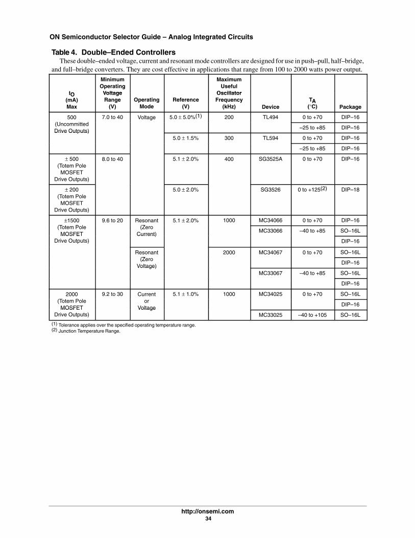
ON Semiconductor Selector Guide – Analog Integrated Circuits
http://onsemi.com 34
Table 4. Double–Ended Controllers These double–ended voltage, current and resonant mode controllers are designed for use in push–pull, half–bridge,
and full–bridge converters. They are cost effective in applications that range from 100 to 2000 watts power output.
IO
MinimumOperating
Voltage
MaximumUseful
OscillatorIO(mA)Max
VoltageRange
(V)Operating
ModeReference
(V)
OscillatorFrequency
(kHz) DeviceTA(°C) Package
500(U i d
7.0 to 40 Voltage 5.0 ± 5.0%(1) 200 TL494 0 to +70 DIP–16(UncommittedDrive Outputs)
–25 to +85 DIP–16Drive Out uts)
5.0 ± 1.5% 300 TL594 0 to +70 DIP–16
–25 to +85 DIP–16
± 500(Totem Pole
MOSFETDrive Outputs)
8.0 to 40 5.1 ± 2.0% 400 SG3525A 0 to +70 DIP–16
± 200(Totem Pole
MOSFETDrive Outputs)
5.0 ± 2.0% SG3526 0 to +125(2) DIP–18
±1500(T P l
9.6 to 20 Resonant(Z
5.1 ± 2.0% 1000 MC34066 0 to +70 DIP–16(Totem Pole
MOSFET(Zero
Current)MC33066 –40 to +85 SO–16L
MOSFETDrive Outputs)
Current)DIP–16
Resonant(Z
2000 MC34067 0 to +70 SO–16L(Zero
Voltage)DIP–16
Voltage)MC33067 –40 to +85 SO–16L
DIP–16
2000(T P l
9.2 to 30 Current 5.1 ± 1.0% 1000 MC34025 0 to +70 SO–16L(Totem Pole
MOSFETor
VoltageDIP–16
MOSFETDrive Outputs)
VoltageMC33025 –40 to +105 SO–16L
(1) Tolerance applies over the specified operating temperature range.(2) Junction Temperature Range.

ON Semiconductor Selector Guide – Analog Integrated Circuits
http://onsemi.com 35
Special Switching Regulator ControllersThese high performance dual channel controllers are
optimized for off–line, ac–to–dc power supplies anddc–to–dc converters in the flyback topology. They alsohave undervoltage lockout voltages which are optimized
for off–line and lower voltage dc–to–dc converters,respectively. Applications include desktop computers,peripherals, televisions, games, and various consumerappliances.
Table 5. Dual Channel Controllers
IO
MinimumOperating
Voltage
MaximumUseful
OscillatorIO(mA)Max
VoltageRange
(V)Operating
ModeReference
(V)
OscillatorFrequency
(kHz) DeviceTA(°C) Package
±1000(T P l
11 to 20 Current 5.0 ± 2.6% 500 MC33065 –40 to +85 SO–16L(Totem Pole
MOSFETDIP–16
MOSFETDrive 8.4 to 20 MC33065 –40 to +85 SO–16L
Outputs) DIP–16
Table 6. Very High Voltage Single–Ended Controller with On–Chip Power Switch This monolithic high voltage switching regulator is specifically designed to operate from a rectified ac line voltage
source. Included are an on–chip high voltage power switch, active off–line startup circuitry and a full featured PWMcontroller with fault protection.
Dev
ice
Rec
tifi
ed 8
5 to
276
VAC
Lin
e
Po
wer
Sw
itch
MO
SF
ET
Inte
gra
ted
Max
Dra
inVo
ltag
e
Pea
kC
urr
ent
RD
S(o
n)
typ
. @ T J
= 25
° C)
( Max
Ou
tpu
t Po
wer
@ V
in=
92V
to
265
VAC
Sta
rt–U
p
Co
ntr
ol
Sch
eme
Osc
illat
or
Fre
qu
ency
Pac
kag
e
Tem
per
atu
reR
ang
e
Ad
dit
ion
alF
eatu
res
MC33362 ONLY110 V
Opera–tion
Yes 500 V 2A 4.4 Ω 20W ActiveOn–Chip
250 VFET
PWM,Fixed
Frequency Voltage
Mode
Adjustableup to
300 kHz
DIP–16SO–16WB
25 to+125°C
MC33363A Yes Yes 700 V 1A 7.5 Ω 14W ActiveOn–Chip
500 VFET
PWM,Fixed
Frequency Voltage
Mode
Adjustableup to
300 kHz
DIP–16SO–16WB
25 to+125°C
MC33363B Yes Yes 700 V 1A 15 Ω 8W ActiveOn–Chip
450 VFET
PWM,Fixed
Frequency Voltage
Mode
Adjustableup to
300 kHz
DIP–16SO–16WB
25 to+125°C
MC33365 Yes Yes 700 V 1A 15 Ω 8W ActiveOn–Chip
450 VFET
PWM,Fixed
Frequency Voltage
Mode
Adjustableup to
300 kHz
DIP–16 25 to+125°C
Bulk CapacitorVoltageSensing
Capability toSense anAC Line
Brown–Out
MC33369 Yes Yes 700 V 0.5A 12 Ω 12W ActiveOn–Chip
700 VFET
PWM,Fixed
Frequency
Fixed @100 kHz
DIP–8TO–220 5
25 to+125°C
ProgrammableState Controllerfor Converter

ON Semiconductor Selector Guide – Analog Integrated Circuits
http://onsemi.com 36
Dev
ice
Ad
dit
ion
alF
eatu
res
Tem
per
atu
reR
ang
e
Pac
kag
e
Osc
illat
or
Fre
qu
ency
Co
ntr
ol
Sch
eme
Sta
rt–U
p
Max
Ou
tpu
t Po
wer
@ V
R inDS
(on
)
= 92
V t
o
Pea
k
265
VAC
typ
. @ T
Cu
rren
t
J
Max
Dra
in
= 25
Volt
age
°
Po
wer
Sw
itch
C)
MO
SF
ET
Inte
gra
ted
(
Rec
tifi
ed 8
5 to
276
VAC
Lin
e
MC33370 Yes Yes 700 V 0.9A 12 Ω 25W ActiveOn–Chip
700 VFET
PWM,Fixed
Frequency
Fixed @100 kHz
DIP–8TO–220 5
25 to+125°C
ProgrammableState Controllerfor Converter
MC33371 Yes Yes 700 V 1.5A 6.8 Ω 45W ActiveOn–Chip
700 VFET
PWM,Fixed
Frequency
Fixed @100 kHz
DIP–8TO–220 5
25 to+125°C
ProgrammableState Controllerfor Converter
MC33372 Yes Yes 700 V 2A 4.8 Ω 60W ActiveOn–Chip
700 VFET
PWM,Fixed
Frequency
Fixed @100 kHz
DIP–8TO–220 5
25 to+125°C
ProgrammableState Controllerfor Converter
MC33373 Yes Yes 700 V 2.7A 3.8 Ω 75W ActiveOn–Chip
700 VFET
PWM,Fixed
Frequency
Fixed @100 kHz
DIP–8TO–220 5
25 to+125°C
ProgrammableState Controllerfor Converter
MC33374 Yes Yes 700 V 3.3A 3.0 Ω 90W ActiveOn–Chip
700 VFET
PWM,Fixed
Frequency
Fixed @100 kHz
DIP–8TO–220 5
25 to+125°C
ProgrammableState Controllerfor Converter

ON Semiconductor Selector Guide – Analog Integrated Circuits
http://onsemi.com 37
Switching Regulator Control Circuits (continued)
Single–Ended GreenLine ControllersEnhanced Mixed Frequency Mode GreenLine PWM Controller:Fixed Frequency, Variable Frequency, Standby Mode
MC44603AP, DW
TA = –25° to +85°C, DIP–16, SO–16L
The MC44603A is an enhanced high performancecontroller that is specifically designed for off–line anddc–to–dc converter applications. This device has theunique ability of automatically changing operatingmodes if the converter output is overloaded, unloaded, orshorted, offering the designer additional protection forincreased system reliability. The MC44603A has severaldistinguishing features when compared to conventionalSMPS controllers. These features consist of a foldbackfacility for overload protection, a standby mode when theconverter output is slightly loaded, a demagnetizationdetection for reduced switching stresses on transistor anddiodes, and a high current totem pole output ideallysuited for driving a power MOSFET. It can also be usedfor driving a bipolar transistor in low power converters(< 150 W). It is optimized to operate in discontinuousmode but can also operate in continuous mode. Itsadvanced design allows use in current mode or voltagemode control applications.
Current or Voltage Mode Controller• Operation up to 250 kHz Output Switching Frequency• Inherent Feed Forward Compensation• Latching PWM for Cycle–by–Cycle Current Limiting• Oscillator with Precise Frequency Control
High Flexibility
• Externally Programmable Reference Current• Secondary or Primary Sensing• Synchronization Facility• High Current Totem Pole Output• Undervoltage Lockout with Hysteresis
Safety/Protection Features
• Overvoltage Protection Against Open Current andOpen Voltage Loop
• Protection Against Short Circuit on Oscillator Pin• Fully Programmable Foldback• Soft–Start Feature• Accurate Maximum Duty Cycle Setting• Demagnetization (Zero Current Detection)
Protection• Internally Trimmed Reference• Enhanced Output Drive
GreenLine Controller: Low Power Consumption inStandby Mode
• Low Startup and Operating Current• Fully Programmable Standby Mode• Controlled Frequency Reduction in Standby Mode• Low dV/dT for Low EMI Radiations
High Safety Standby Ladder Mode GreenLine PWM Controller
MC44604P
TA = –25° to +85°C, DIP–16
The MC44604 is an enhanced high performancecontroller that is specifically designed for off–line anddc–to–dc converter applications.
The MC44604 is a modification of the MC44603. TheMC44604 offers enhanced safety and reliable powermanagement in its protection features (foldback, over-voltage detection, soft–start, accurate demagnetizationdetection). Its high current totem pole output is alsoideally suited for driving a power MOSFET but can alsobe used for driving a bipolar transistor in low power con-verters (< 150 W).
In addition, the MC44604 offers a new efficient wayto reduce the standby operating power by means of a
patented standby ladder mode operation of the convertersignificantly reducing the converter consumption instandby mode.
Current or Voltage Mode Controller• Operation Up to 250 kHz Output Switching Frequency• Inherent Feed Forward Compensation• Latching PWM for Cycle–by–Cycle Current Limiting• Oscillator with Precise Frequency Control
High Flexibility• Externally Programmable Reference Current• Secondary or Primary Sensing• High Current Totem Pole Output• Undervoltage Lockout with Hysteresis

ON Semiconductor Selector Guide – Analog Integrated Circuits
http://onsemi.com 38
Single–Ended GreenLine Controllers (continued)
High Safety Standby Ladder Mode GreenLine PWM Controller (continued)
Safety/Protection Features• Overvoltage Protection Facility Against Open Loop• Protection Against Short Circuit on Oscillator Pin• Fully Programmable Foldback• Soft–Start Feature• Accurate Maximum Duty Cycle Setting• Demagnetization (Zero Current Detection) Protection
• Internally Trimmed Reference
GreenLine Controller:
• Low Startup and Operating Current• Patented Standby Ladder Mode for Low Standby
Losses• Low dV/dT for Low EMI
High Safety Latched Mode GreenLine PWM Controllerfor (Multi)Synchronized Applications
MC44605P
TA = –25° to +85°C, DIP–16
The MC44605 is a high performance current modecontroller that is specifically designed for off–lineconverters. The MC44605 has several distinguishingfeatures that make it particularly suitable formultisynchronized monitor applications.
The MC44605 synchronization arrangementenables operation from 16 kHz up to 130 kHz. Thisproduct was optimized to operate with universal acmains voltage from 80 V to 280 V, and its high currenttotem pole output makes it ideally suited for driving apower MOSFET.
The MC44605 protections provide well controlled,safe power management. Safety enhancements detectfour different fault conditions and provide protectionthrough a disabling latch.
Current or Voltage Mode Controller
• Current Mode Operation Up to 250 kHz OutputSwitching Frequency
• Inherent Feed Forward Compensation• Latching PWM for Cycle–by–Cycle Current
Limiting• Oscillator with Precise Frequency Control• Externally Programmable Reference Current• Secondary or Primary Sensing (Availability of Error
Amplifier Output)• Synchronization Facility
• High Current Totem Pole Output• Undervoltage Lockout with Hysteresis• Low Output dV/dT for Low EMI• Low Startup and Operating Current
Safety/Protection Features• Soft–Start Feature• Demagnetization (Zero Current Detection)
Protection• Overvoltage Protection Facility Against Open Loop• EHT Overvoltage Protection (E.H.T.OVP):
Protection Against Excessive AmplitudeSynchronization Pulses
• Winding Short Circuit Detection (W.S.C.D.)• Limitation of the Maximum Input Power (M.P.L.):
Calculation of Input Power for Overload Protection• Over Heating Detection (O.H.D.): to Prevent the
Power Switch from Excessive Heating
Latched Disabling Mode• When one of the following faults is detected: EHT
overvoltage, Winding Short Circuit (WSCD),excessive input power (M.P.L.), power switch overheating (O.H.D.), a counter is activated
• If the counter is activated for a time that is longenough, the circuit gets definitively disabled. Thelatch can only be reset by removing and thenre–applying power

ON Semiconductor Selector Guide – Analog Integrated Circuits
http://onsemi.com 39
Few External ComponentsReliable and FlexibleGreenLine Very High VoltagePWM Controller
MC44608
TA = –25° to +85°C, DIP–8
The MC44608 is a high performance voltage modecontroller designed for off–line converters. This highvoltage circuit that integrates the start–up current sourceand the oscillator capacitor, requires few external com-ponents while offering a high flexibility and reliability.
The device also features a very high efficiencystand–by management consisting of an effective PulsedMode operation. This technique enables the reduction ofthe stand–by power consumption to approximately 1Wwhile delivering 300mW in a 150W SMPS.
• Integrated Start–Up Current Source• Lossless Off–Line Start–Up• Direct Off–Line Operation• Fast Start–Up
General Features
• Flexibility• Duty Cycle Control
• Undervoltage Lockout with Hysteresis• On Chip Oscillator Switching Frequency 40, 75, or
100kHz• Secondary control with Few External Components
Protections• Maximum Duty Cycle Limitation• Cycle by Cycle Current Limitation• Demagnetization (Zero Current Detection)
Protection• “Over VCC Protection” Against Open Loop• Programmable Low Inertia Over Voltage Protection
against open loop• Internal Thermal Protection
GreenLine Controller• Pulsed Mode Techniques for a Very High Efficiency
Low Power Mode• Lossless Startup• Low dV/dT for Low EMI Radiations
ORDERING INFORMATION
DeviceOperating
Temperature Range Package
MC44608P40Pl ti
MC44608P75 TJ = –25° to +85°CPlasticDIP–8
MC44608P100DIP 8

ON Semiconductor Selector Guide – Analog Integrated Circuits
http://onsemi.com 40
Representative Block Diagram
+–
+
–
+
–
DMG
DemagLogic
OutputStart–upPhase
SwitchingPhase
LatchedPhase
1 V 10 kHz Filter
RegulationBlock
Switching Phase
S2 S3&
Latched off PhaseStand–by
Thermal
DMGOUT Disable
OVPUVLO1
Switching Phase
Start–up Phase
Latched off Phase
UVLO210 mA Start–up
CC
Buffer
PWM
QR
S
&
&
PWM
VPWM&
OSC
OSCClock
Stand–by
Leading Edge
S1
1 0
&Stand–by
1 8
6
5
4
3
2
Demag Vi
Isense
Control
GND
Driver
V
Input
CC
Shutdown
Latch
UVLO2
ManagementV
&
Source
Management
Enable
Blanking Output
CS
2 S
>120 A>24 A50 mV/20 mV
NOCOC
200 AStart–upPhase

ON Semiconductor Selector Guide – Analog Integrated Circuits
http://onsemi.com 41
Switching Regulator Control Circuits (continued)
Very High Voltage Switching Regulator
MC33362DW, P
TJ = –25° to +125°C, DIP–16, SOP–16L
The MC33362 is a monolithic high voltage switchingregulator that is specifically designed to operate from arectified 120 VAC line source. This integrated circuitfeatures an on–chip 500 V/2.0 A SenseFET powerswitch, 250 V active off–line startup FET, duty cyclecontrolled oscillator, current limiting comparator with aprogrammable threshold and leading edge blanking,latching pulse width modulator for double pulsesuppression, high gain error amplifier, and a trimmedinternal bandgap reference. Protective features includecycle–by–cycle current limiting, input undervoltagelockout with hysteresis, output overvoltage protection,
and thermal shutdown. This device is available in a16–lead dual–in–line and wide body surface mountpackages.• On–Chip 500 V, 2.0 A SenseFET Power Switch• Rectified 120 VAC Line Source Operation• On–Chip 250 V Active Off–Line Startup FET• Latching PWM for Double Pulse Suppression• Cycle–By–Cycle Current Limiting• Input Undervoltage Lockout with Hysteresis• Output Overvoltage Protection Comparator• Trimmed Internal Bandgap Reference• Internal Thermal Shutdown
20 W Off–Line Converter
Startup
Reg
Osc
Thermal
LEB
PWM
DC Output
Startup Input
Gnd 4, 5, 12, 13
Mirror
7
AC Input
RegulatorOutput
6
8
CT
RT
PWM Latch
EA
Ipk
VCC
3
11
16
9
10
1
Compensation
Voltage FeedbackInput
Power SwitchDrain
OvervoltageProtection Input
Driver
OVP
UVLO
S
R
Q

ON Semiconductor Selector Guide – Analog Integrated Circuits
http://onsemi.com 42
Switching Regulator Control Circuits (continued)
Very High Voltage Switching RegulatorMC33363ADW, AP
TJ = –25° to +125°C, DIP–16, SOP–16L
The MC33363A is a monolithic high voltage switchingregulator that is specifically designed to operate from a rec-tified 240 Vac line source. This integrated circuit features anon–chip 700 V/1.5 A SenseFET power switch, 550 V activeoff–line startup FET, duty cycle controlled oscillator, cur-rent limiting comparator with a programmable thresholdand leading edge blanking, latching pulse width modulatorfor double pulse suppression, high gain error amplifier, anda trimmed internal bandgap reference. Protective featuresinclude cycle–by–cycle current limiting, input undervol-tage lockout with hysteresis, output overvoltage protection,
and thermal shutdown. This device is available in a 16–leaddual–in–line and wide body surface mount packages.• On–Chip 700 V, 1.5 A SenseFET Power Switch• Rectified 240 Vac Line Source Operation• On–Chip 500 V Active Off–Line Startup FET• Latching PWM for Double Pulse Suppression• Cycle–By–Cycle Current Limiting• Input Undervoltage Lockout with Hysteresis• Output Overvoltage Protection Comparator• Trimmed Internal Bandgap Reference• Internal Thermal Shutdown
Startup
Reg
Osc
Thermal
LEB
PWM
DC Output
Startup Input
Gnd 4, 5, 12, 13
Mirror
7
AC Input
RegulatorOutput
6
8
CT
RT
PWM Latch
EA
Ipk
VCC
3
11
16
9
10
1
Compensation
VoltageFeedbackInput
Power SwitchDrain
OvervoltageProtection Input
Driver
OVP
UVLO
S
R
Q
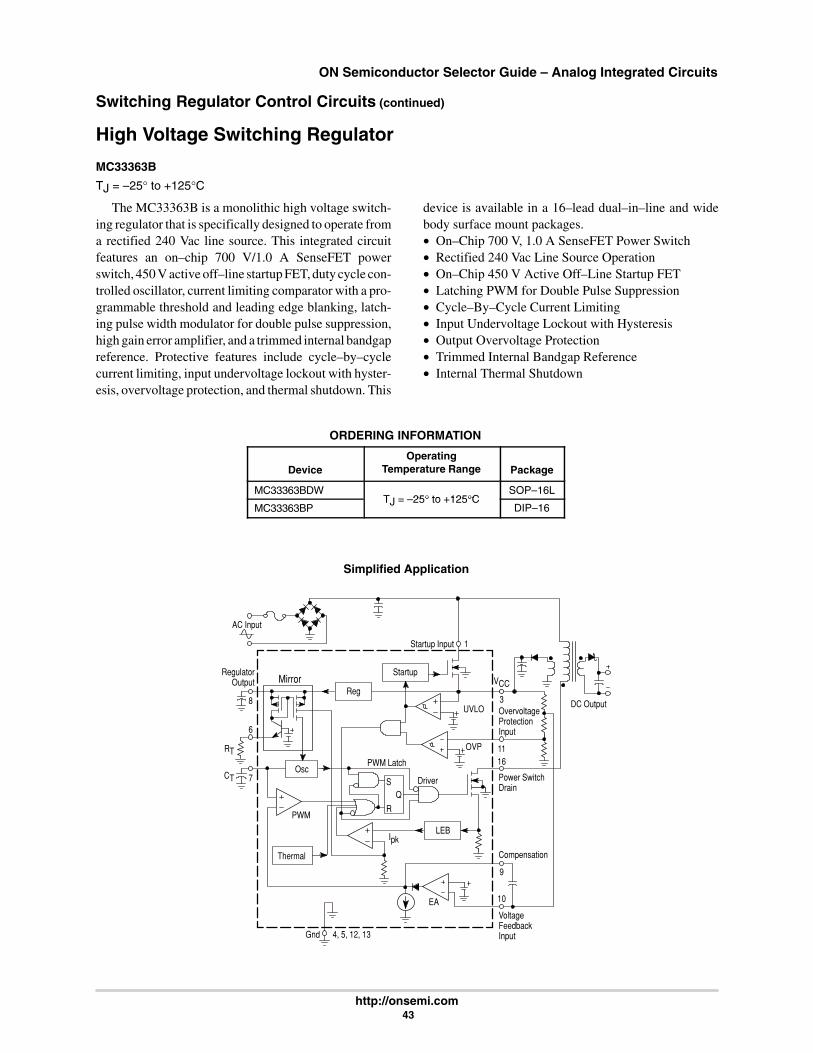
ON Semiconductor Selector Guide – Analog Integrated Circuits
http://onsemi.com 43
Switching Regulator Control Circuits (continued)
High Voltage Switching Regulator
MC33363B
TJ = –25° to +125°C
The MC33363B is a monolithic high voltage switch-ing regulator that is specifically designed to operate froma rectified 240 Vac line source. This integrated circuitfeatures an on–chip 700 V/1.0 A SenseFET powerswitch, 450 V active off–line startup FET, duty cycle con-trolled oscillator, current limiting comparator with a pro-grammable threshold and leading edge blanking, latch-ing pulse width modulator for double pulse suppression,high gain error amplifier, and a trimmed internal bandgapreference. Protective features include cycle–by–cyclecurrent limiting, input undervoltage lockout with hyster-esis, overvoltage protection, and thermal shutdown. This
device is available in a 16–lead dual–in–line and widebody surface mount packages.• On–Chip 700 V, 1.0 A SenseFET Power Switch• Rectified 240 Vac Line Source Operation• On–Chip 450 V Active Off–Line Startup FET• Latching PWM for Double Pulse Suppression• Cycle–By–Cycle Current Limiting• Input Undervoltage Lockout with Hysteresis• Output Overvoltage Protection• Trimmed Internal Bandgap Reference• Internal Thermal Shutdown
ORDERING INFORMATION
DeviceOperating
Temperature Range Package
MC33363BDWTJ = 25° to +125°C
SOP–16L
MC33363BPTJ = –25° to +125°C
DIP–16
Simplified Application
Startup
Reg
Osc
Thermal
LEB
PWM
DC Output
Startup Input
Gnd 4, 5, 12, 13
Mirror
7
AC Input
RegulatorOutput
6
8
CT
RTPWM Latch
EA
Ipk
VCC
3
1116
9
10
1
Compensation
VoltageFeedbackInput
Power SwitchDrain
OvervoltageProtectionInput
Driver
OVP
UVLO
S
R
Q
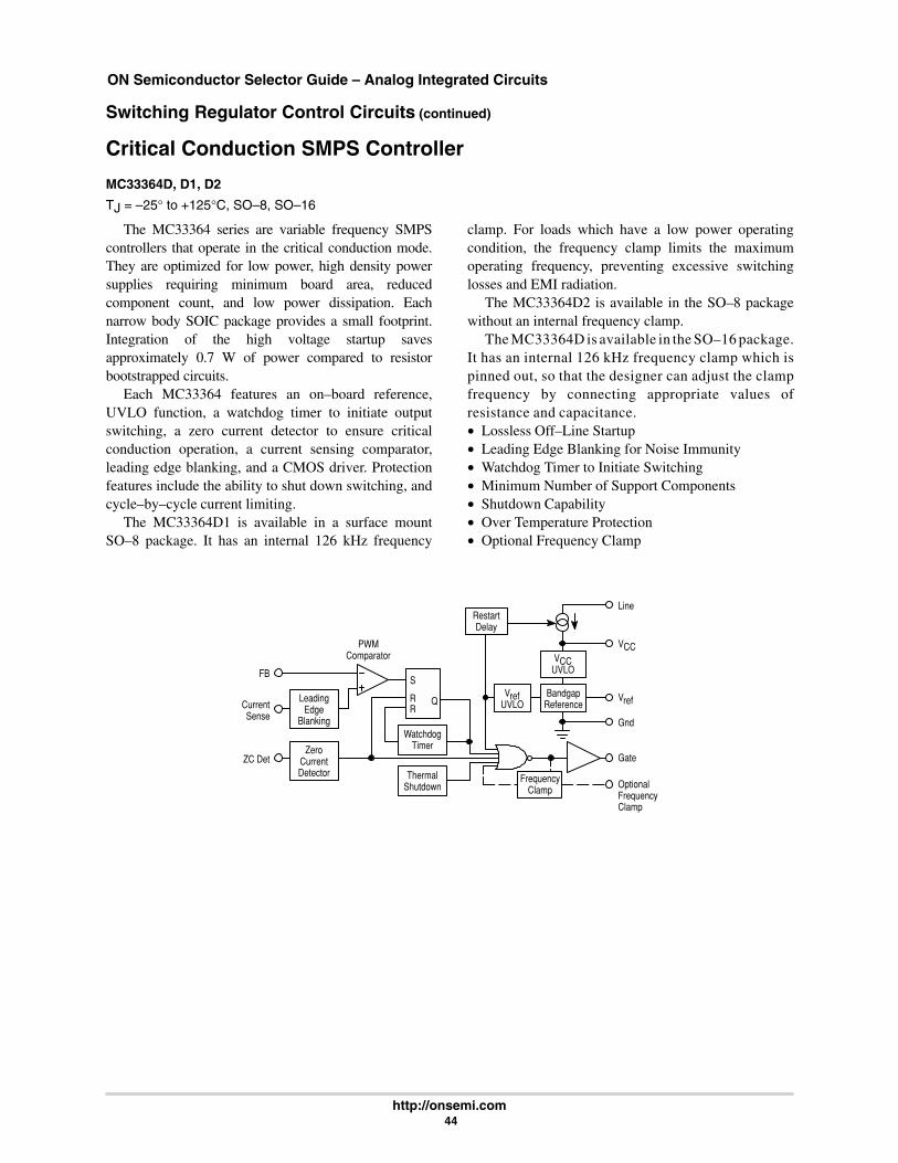
ON Semiconductor Selector Guide – Analog Integrated Circuits
http://onsemi.com 44
Switching Regulator Control Circuits (continued)
Critical Conduction SMPS Controller
MC33364D, D1, D2
TJ = –25° to +125°C, SO–8, SO–16
The MC33364 series are variable frequency SMPScontrollers that operate in the critical conduction mode.They are optimized for low power, high density powersupplies requiring minimum board area, reducedcomponent count, and low power dissipation. Eachnarrow body SOIC package provides a small footprint.Integration of the high voltage startup savesapproximately 0.7 W of power compared to resistorbootstrapped circuits.
Each MC33364 features an on–board reference,UVLO function, a watchdog timer to initiate outputswitching, a zero current detector to ensure criticalconduction operation, a current sensing comparator,leading edge blanking, and a CMOS driver. Protectionfeatures include the ability to shut down switching, andcycle–by–cycle current limiting.
The MC33364D1 is available in a surface mountSO–8 package. It has an internal 126 kHz frequency
clamp. For loads which have a low power operatingcondition, the frequency clamp limits the maximumoperating frequency, preventing excessive switchinglosses and EMI radiation.
The MC33364D2 is available in the SO–8 packagewithout an internal frequency clamp.
The MC33364D is available in the SO–16 package.It has an internal 126 kHz frequency clamp which ispinned out, so that the designer can adjust the clampfrequency by connecting appropriate values ofresistance and capacitance.• Lossless Off–Line Startup• Leading Edge Blanking for Noise Immunity• Watchdog Timer to Initiate Switching• Minimum Number of Support Components• Shutdown Capability• Over Temperature Protection• Optional Frequency Clamp
CurrentSense
FB
ZC Det
VCC
Gate
PWMComparator
S
R Q
Gnd
Line
VrefVref
UVLO
RestartDelay
RLeading
EdgeBlanking
ZeroCurrentDetector
WatchdogTimer
ThermalShutdown
BandgapReference
VCCUVLO
FrequencyClamp Optional
FrequencyClamp
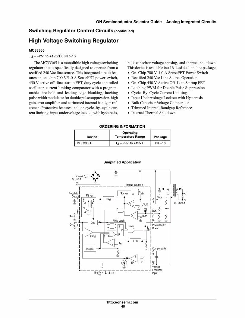
ON Semiconductor Selector Guide – Analog Integrated Circuits
http://onsemi.com 45
Switching Regulator Control Circuits (continued)
High Voltage Switching Regulator
MC33365
TJ = –25° to +125°C, DIP–16
The MC33365 is a monolithic high voltage switchingregulator that is specifically designed to operate from arectified 240 Vac line source. This integrated circuit fea-tures an on–chip 700 V/1.0 A SenseFET power switch,450 V active off–line startup FET, duty cycle controlledoscillator, current limiting comparator with a program-mable threshold and leading edge blanking, latchingpulse width modulator for double pulse suppression, highgain error amplifier, and a trimmed internal bandgap ref-erence. Protective features include cycle–by–cycle cur-rent limiting, input undervoltage lockout with hysteresis,
bulk capacitor voltage sensing, and thermal shutdown.This device is available in a 16–lead dual–in–line package.• On–Chip 700 V, 1.0 A SenseFET Power Switch• Rectified 240 Vac Line Source Operation• On–Chip 450 V Active Off–Line Startup FET• Latching PWM for Double Pulse Suppression• Cycle–By–Cycle Current Limiting• Input Undervoltage Lockout with Hysteresis• Bulk Capacitor Voltage Comparator• Trimmed Internal Bandgap Reference• Internal Thermal Shutdown
ORDERING INFORMATION
DeviceOperating
Temperature Range Package
MC33365P TJ = –25° to +125°C DIP–16
Simplified Application
Startup
Reg
Osc
Thermal
LEB
PWM
DC Output
Startup Input
Gnd 4, 5, 12, 13
Mirror
7
AC Input
RegulatorOutput
6
8
CT
RTPWM Latch
EA
Ipk
VCC3
1116
9
10
1
Compensation
VoltageFeedbackInput
Power SwitchDrain
BOK
Driver
BOK
UVLO
S
R
Q
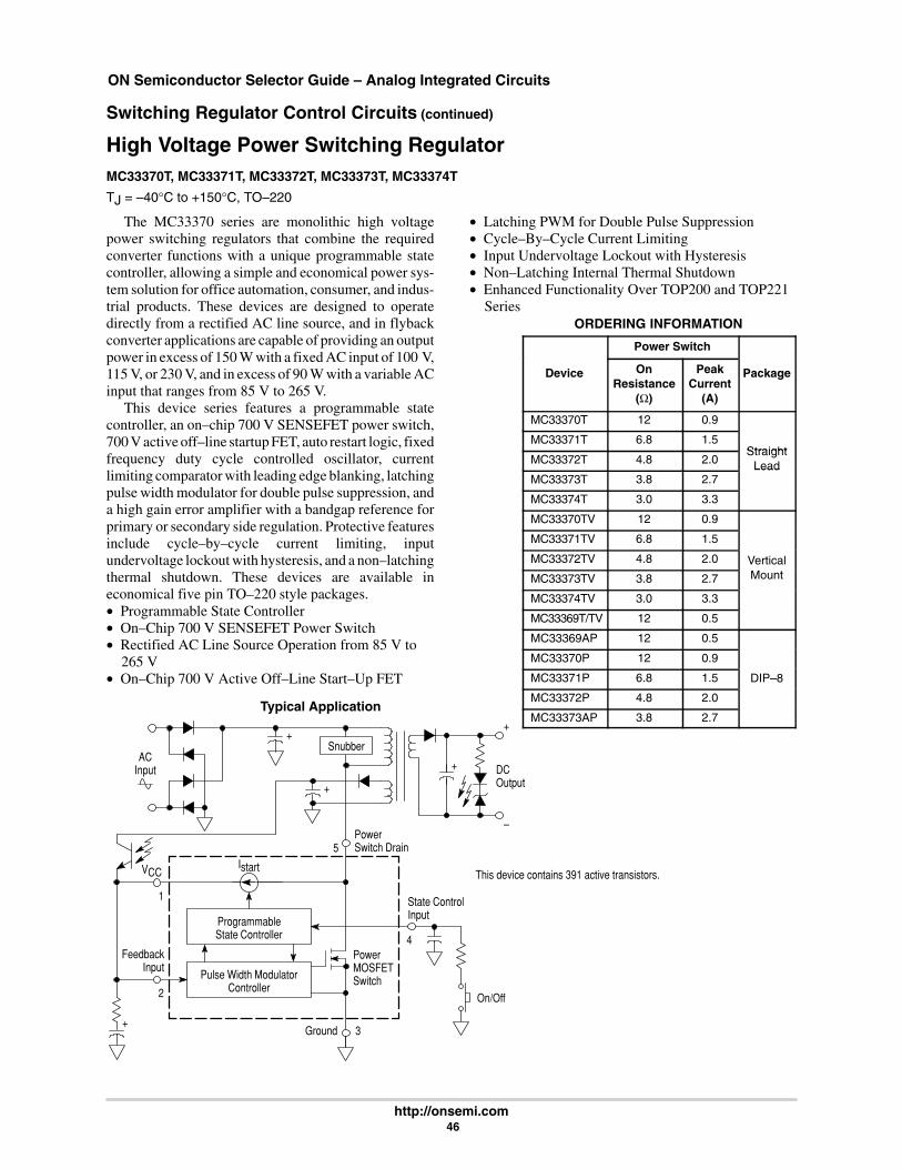
ON Semiconductor Selector Guide – Analog Integrated Circuits
http://onsemi.com 46
Switching Regulator Control Circuits (continued)
High Voltage Power Switching RegulatorMC33370T, MC33371T, MC33372T, MC33373T, MC33374T
TJ = –40°C to +150°C, TO–220
The MC33370 series are monolithic high voltagepower switching regulators that combine the requiredconverter functions with a unique programmable statecontroller, allowing a simple and economical power sys-tem solution for office automation, consumer, and indus-trial products. These devices are designed to operatedirectly from a rectified AC line source, and in flybackconverter applications are capable of providing an outputpower in excess of 150 W with a fixed AC input of 100 V,115 V, or 230 V, and in excess of 90 W with a variable ACinput that ranges from 85 V to 265 V.
This device series features a programmable statecontroller, an on–chip 700 V SENSEFET power switch,700 V active off–line startup FET, auto restart logic, fixedfrequency duty cycle controlled oscillator, currentlimiting comparator with leading edge blanking, latchingpulse width modulator for double pulse suppression, anda high gain error amplifier with a bandgap reference forprimary or secondary side regulation. Protective featuresinclude cycle–by–cycle current limiting, inputundervoltage lockout with hysteresis, and a non–latchingthermal shutdown. These devices are available ineconomical five pin TO–220 style packages.• Programmable State Controller• On–Chip 700 V SENSEFET Power Switch• Rectified AC Line Source Operation from 85 V to
265 V• On–Chip 700 V Active Off–Line Start–Up FET
• Latching PWM for Double Pulse Suppression• Cycle–By–Cycle Current Limiting• Input Undervoltage Lockout with Hysteresis• Non–Latching Internal Thermal Shutdown• Enhanced Functionality Over TOP200 and TOP221
SeriesORDERING INFORMATION
Power Switch
Device OnResistance
(Ω)
PeakCurrent
(A)
Package
MC33370T 12 0.9
MC33371T 6.8 1.5Straight
MC33372T 4.8 2.0Straight
LeadMC33373T 3.8 2.7
Lead
MC33374T 3.0 3.3
MC33370TV 12 0.9
MC33371TV 6.8 1.5
MC33372TV 4.8 2.0 Vertical
MC33373TV 3.8 2.7 Mount
MC33374TV 3.0 3.3
MC33369T/TV 12 0.5
MC33369AP 12 0.5
MC33370P 12 0.9
MC33371P 6.8 1.5 DIP–8
MC33372P 4.8 2.0
MC33373AP 3.8 2.7Typical Application
This device contains 391 active transistors.
ProgrammableState Controller
Pulse Width ModulatorController
PowerMOSFETSwitch
Snubber
FeedbackInput
VCC
Ground
PowerSwitch Drain
+
+
++
–
DCOutput
2
1
5
State ControlInput
On/Off
4
3
Istart
ACInput
+
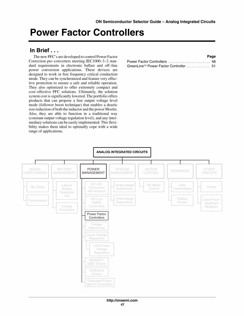
ANALOG INTEGRATED CIRCUITS
SIGNALCONDITIONING
BATTERYMANAGEMENT
POWERMANAGEMENT
SYSTEMMANAGEMENT
MOTORCONTROL INTERFACE OTHER
CIRCUITS
Op–Amps
Comparators
LithiumBattery
ProtectionICs
ChargeControllers
DC–DCConverters
with Inductor
Off–LineSMPS
Controllers
UndervoltageSupervisory
OvervoltageSupervisory
DataTransmission
DisplayDrivers
Timers
Linear Four–QuadrantMultiplier
Power FactorControllers
VoltageReferences
Linear VoltageRegulators
LDO LinearVoltage
Regulators
MOSFET/IGBT Drivers
DedicatedDrivers
Dedicated PowerMgmnt Controllers
DC MotorControl
ON Semiconductor Selector Guide – Analog Integrated Circuits
http://onsemi.com 47
Power Factor Controllers
In Brief . . .The new PFC’s are developed to control Power Factor
Correction pre–converters meeting IEC1000–3–2 stan-dard requirements in electronic ballast and off–linepower conversion applications. These devices aredesigned to work in free frequency critical conductionmode. They can be synchronized and feature very effec-tive protection to ensure a safe and reliable operation.They also optimized to offer extremely compact andcost–effective PFC solutions. Ultimately, the solutionsystem cost is significantly lowered. The portfolio offersproducts that can propose a free output voltage levelmode (follower boost technique) that enables a drasticsize reduction of both the inductor and the power Mosfet.Also, they are able to function in a traditional way(constant output voltage regulation level), and any inter-mediary solutions can be easily implemented. This flexi-bility makes them ideal to optimally cope with a widerange of applications.
PagePower Factor Controllers 48. . . . . . . . . . . . . . . . . . . . . . . GreenLine Power Factor Controller 51. . . . . . . . . . . . .
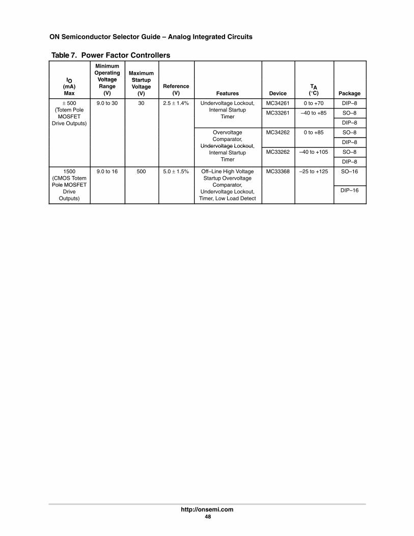
ON Semiconductor Selector Guide – Analog Integrated Circuits
http://onsemi.com 48
Table 7. Power Factor Controllers
IO
MinimumOperating
VoltageMaximumStart pIO
(mA)Max
VoltageRange
(V)
StartupVoltage
(V)Reference
(V) Features DeviceTA(°C) Package
± 500(T P l
9.0 to 30 30 2.5 ± 1.4% Undervoltage Lockout,I l S
MC34261 0 to +70 DIP–8(Totem Pole
MOSFETInternal Startup
TimerMC33261 –40 to +85 SO–8
MOSFETDrive Outputs)
TimerDIP–8
OvervoltageC
MC34262 0 to +85 SO–8Comparator,
Undervoltage LockoutDIP–8
Undervoltage Lockout,Internal Startup MC33262 –40 to +105 SO–8
Timer DIP–8
1500(CMOS TotemPole MOSFET
9.0 to 16 500 5.0 ± 1.5% Off–Line High VoltageStartup Overvoltage
Comparator
MC33368 –25 to +125 SO–16
Pole MOSFETDrive
Outputs)
Com arator,Undervoltage Lockout,Timer, Low Load Detect
DIP–16
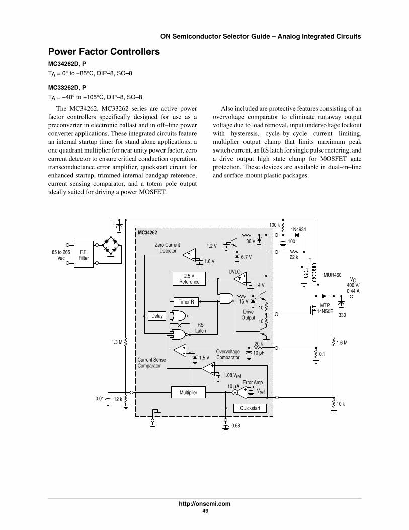
ON Semiconductor Selector Guide – Analog Integrated Circuits
http://onsemi.com 49
Power Factor ControllersMC34262D, P
TA = 0° to +85°C, DIP–8, SO–8
MC33262D, P
TA = –40° to +105°C, DIP–8, SO–8
The MC34262, MC33262 series are active powerfactor controllers specifically designed for use as apreconverter in electronic ballast and in off–line powerconverter applications. These integrated circuits featurean internal startup timer for stand alone applications, aone quadrant multiplier for near unity power factor, zerocurrent detector to ensure critical conduction operation,transconductance error amplifier, quickstart circuit forenhanced startup, trimmed internal bandgap reference,current sensing comparator, and a totem pole outputideally suited for driving a power MOSFET.
Also included are protective features consisting of anovervoltage comparator to eliminate runaway outputvoltage due to load removal, input undervoltage lockoutwith hysteresis, cycle–by–cycle current limiting,multiplier output clamp that limits maximum peakswitch current, an RS latch for single pulse metering, anda drive output high state clamp for MOSFET gateprotection. These devices are available in dual–in–lineand surface mount plastic packages.
14 V
0.68
1.5 V
Error Amp
OvervoltageComparator
1.08 Vref
Quickstart
10 µA
10 pF
20 k
1.6 V
Timer R
330
100
MTP14N50E
1.3 M
RFIFilter
0.01
MC34262
6.7 V
Zero Current Detector
T
UVLO
Current Sense Comparator
RSLatch
1.2 V36 V
2.5 VReference
16 V10
DriveOutput
Multiplier
Delay
85 to 265Vac
1
12 k
22 k
100 k1N4934
10 k
1.6 M
0.1
MUR460VO
400 V/0.44 A
Vref
10
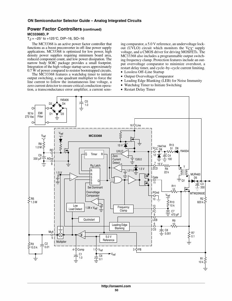
ON Semiconductor Selector Guide – Analog Integrated Circuits
http://onsemi.com 50
Power Factor Controllers (continued)MC33368D, PTJ = –25° to +125°C, DIP–16, SO–16
The MC33368 is an active power factor controller thatfunctions as a boost preconverter in off–line power supplyapplications. MC33368 is optimized for low power, highdensity power supplies requiring minimum board area,reduced component count, and low power dissipation. Thenarrow body SOIC package provides a small footprint.Integration of the high voltage startup saves approximately0.7 W of power compared to resistor bootstrapped circuits.
The MC33368 features a watchdog timer to initiateoutput switching, a one quadrant multiplier to force theline current to follow the instantaneous line voltage, azero current detector to ensure critical conduction opera-tion, a transconductance error amplifier, a current sens-
ing comparator, a 5.0 V reference, an undervoltage lock-out (UVLO) circuit which monitors the VCC supplyvoltage, and a CMOS driver for driving MOSFETs. TheMC33368 also includes a programmable output switch-ing frequency clamp. Protection features include an out-put overvoltage comparator to minimize overshoot, arestart delay timer, and cycle–by–cycle current limiting.• Lossless Off–Line Startup• Output Overvoltage Comparator• Leading Edge Blanking (LEB) for Noise Immunity• Watchdog Timer to Initiate Switching• Restart Delay Timer
Multiplier
8
C11.0
FrequencyClamp
R
SQ
R
SS
Timer R
Vref
Leading EdgeBlanking
LowLoad Detect
Comp FB
6LEB
13
PGnd
Gate
ZCD
VCC
Line
RD
AGnd
MC33368
16
12
7
11
10
FC9
314
Quickstart
OvervoltageComparator
Set Dominant
1.5 V
15 V
Q
5.0 VReference
MUR460D5
C3330
MTW20N50E
Q1
D6
C4100
TR4
22 k
EMIFilter
92 to 270 Vac
R70.1
C51.0
R51.3 M
R310.5 k
C20.01
R110 k
R2820 k
R81.0 M
C9330 µF
D1 D3
D2 D4
R1110
15 V
C60.1
13/8.0
UVLO
1.2/1.0
R1351D8
RS Latch
Vref
Vref
Vref
CS
2
5
Mult
1.5 V
ZeroCurrentDetect
1.08 x Vref
1N5406
R1010 k
C7470 pF
Vref
C80.001
R910
1N4744
1N4934

ON Semiconductor Selector Guide – Analog Integrated Circuits
http://onsemi.com 51
GreenLine Power Factor Controller
MC33260P
The MC33260 is developed to control Power FactorCorrection preconverters meeting IEC1000–3–2 stan-dard requirements in electronic ballast and off–linepower conversion applications. Designed to work in freefrequency critical conduction mode, it can also be syn-chronized and in any case, it features very effectiveprotections to ensure a safe and reliable operation.
This circuit is also optimized to offer extremelycompact and cost–effective PFC solutions. In effect,while requiring a minimum number of externalcomponents, the MC33260 also proposes a free outputvoltage level mode (follower boost technique) thatenables a drastic size reduction of both the inductor andthe power mosfet. Ultimately, the solution system cost issignificantly lowered.
Also able to function in traditional way (constantoutput voltage regulation level), any intermediarysolutions can be easily implemented. This flexibilitymakes it ideal to optimally cope with a wide range ofapplications.
General Features
• “Free Level’’ or Traditional Constant Output LevelMode
• Switch Mode Operation: Voltage Mode• Latching PWM for Cycle–by–Cycle On–Time
Control• Totem Pole Gate Drive• Undervoltage Lockout with Hysteresis• Low Start–up and Operating Current• Improved Regulation Block Dynamic Behaviour• Synchronization Facility• Internally Trimmed Reference Current Source
Safety/Protection Features
• Overvoltage Protection: Output OvervoltageDetection
• Undervoltage Protection: Protection Against OpenLoop
• Accurate Demagnetization (Zero Current Detection)Protection
• Precise and Adjustable Maximum On–TimeLimitation
• Over Current Protection
ORDERING INFORMATION
Device Temperature Range Package
MC33260P –40° to +105°C Plastic DIP–8
Typical Application
Load(SMPS, LampBallast, . . .)Ro
C1+
D1
Q1
Vcc8
MC3
3260
1
2
3
4
7
6
5sync
CT
Rcs
Vcontrol
Rs
1 µFD1 . . . D4
GreenLine is a trademark of Semiconductor Components Industries, LLC (SCILLC)
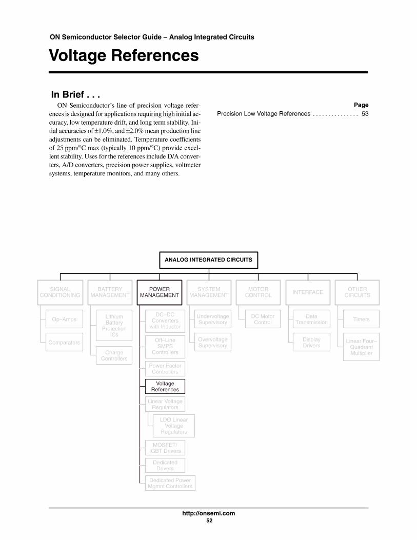
ANALOG INTEGRATED CIRCUITS
SIGNALCONDITIONING
BATTERYMANAGEMENT
POWERMANAGEMENT
SYSTEMMANAGEMENT
MOTORCONTROL INTERFACE OTHER
CIRCUITS
Op–Amps
Comparators
LithiumBattery
ProtectionICs
ChargeControllers
DC–DCConverters
with Inductor
Off–LineSMPS
Controllers
UndervoltageSupervisory
OvervoltageSupervisory
DataTransmission
DisplayDrivers
Timers
Linear Four–QuadrantMultiplier
Power FactorControllers
VoltageReferences
Linear VoltageRegulators
LDO LinearVoltage
Regulators
MOSFET/IGBT Drivers
DedicatedDrivers
Dedicated PowerMgmnt Controllers
DC MotorControl
ON Semiconductor Selector Guide – Analog Integrated Circuits
http://onsemi.com 52
Voltage References
In Brief . . .ON Semiconductor’s line of precision voltage refer-
ences is designed for applications requiring high initial ac-curacy, low temperature drift, and long term stability. Ini-tial accuracies of ±1.0%, and ±2.0% mean production lineadjustments can be eliminated. Temperature coefficientsof 25 ppm/°C max (typically 10 ppm/°C) provide excel-lent stability. Uses for the references include D/A conver-ters, A/D converters, precision power supplies, voltmetersystems, temperature monitors, and many others.
PagePrecision Low Voltage References 53. . . . . . . . . . . . . . .
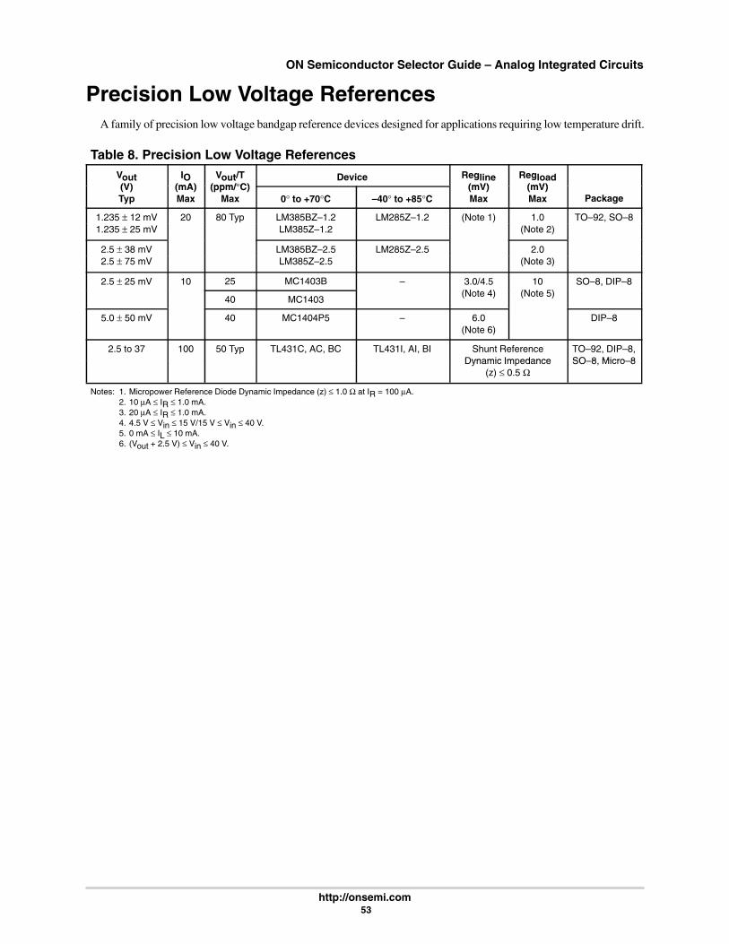
ON Semiconductor Selector Guide – Analog Integrated Circuits
http://onsemi.com 53
Precision Low Voltage ReferencesA family of precision low voltage bandgap reference devices designed for applications requiring low temperature drift.
Table 8. Precision Low Voltage ReferencesVout(V)
IO(mA)
Vout/T(ppm/°C)
Device Regline(mV)
Regload(mV)(V)
Typ(mA)Max
(ppm/°C)Max 0° to +70°C –40° to +85°C
(mV)Max
(mV)Max Package
1.235 ± 12 mV 20 80 Typ LM385BZ–1.2 LM285Z–1.2 (Note 1) 1.0 TO–92, SO–81.235 ± 25 mV
yLM385Z–1.2
( )(Note 2)
2.5 ± 38 mV LM385BZ–2.5 LM285Z–2.5 2.02.5 ± 75 mV LM385Z–2.5 (Note 3)
2.5 ± 25 mV 10 25 MC1403B – 3.0/4.5(N 4)
10(N 5)
SO–8, DIP–8
40 MC1403(Note 4) (Note 5)
5.0 ± 50 mV 40 MC1404P5 – 6.0(Note 6)
DIP–8
2.5 to 37 100 50 Typ TL431C, AC, BC TL431I, AI, BI Shunt ReferenceDynamic Impedance
TO–92, DIP–8,SO–8 Micro–8Dynamic Im edance
(z) ≤ 0.5 ΩSO–8, Micro–8
Notes: 1. Micropower Reference Diode Dynamic Impedance (z) ≤ 1.0 Ω at IR = 100 µA.2. 10 µA ≤ IR ≤ 1.0 mA.3. 20 µA ≤ IR ≤ 1.0 mA.4. 4.5 V ≤ Vin ≤ 15 V/15 V ≤ Vin ≤ 40 V.5. 0 mA ≤ IL ≤ 10 mA.6. (Vout + 2.5 V) ≤ Vin ≤ 40 V.
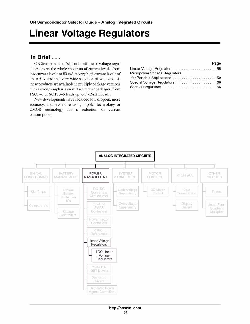
ANALOG INTEGRATED CIRCUITS
SIGNALCONDITIONING
BATTERYMANAGEMENT
POWERMANAGEMENT
SYSTEMMANAGEMENT
MOTORCONTROL INTERFACE OTHER
CIRCUITS
Op–Amps
Comparators
LithiumBattery
ProtectionICs
ChargeControllers
DC–DCConverters
with Inductor
Off–LineSMPS
Controllers
UndervoltageSupervisory
OvervoltageSupervisory
DataTransmission
DisplayDrivers
Timers
Linear Four–QuadrantMultiplier
Power FactorControllers
VoltageReferences
Linear VoltageRegulators
LDO LinearVoltage
Regulators
MOSFET/IGBT Drivers
DedicatedDrivers
Dedicated PowerMgmnt Controllers
DC MotorControl
ON Semiconductor Selector Guide – Analog Integrated Circuits
http://onsemi.com 54
Linear Voltage Regulators
In Brief . . .ON Semiconductor’s broad portfolio of voltage regu-
lators covers the whole spectrum of current levels, fromlow current levels of 80 mA to very high current levels ofup to 5 A, and in a very wide selection of voltages. Allthese products are available in multiple package versionswith a strong emphasis on surface mount packages, fromTSOP–5 or SOT23–5 leads up to D2PAK 5 leads.
New developments have included low dropout, moreaccuracy, and less noise using bipolar technology orCMOS technology for a reduction of currentconsumption.
PageLinear Voltage Regulators 55. . . . . . . . . . . . . . . . . . . . . . Micropower Voltage Regulatorsfor Portable Applications 59. . . . . . . . . . . . . . . . . . . . . . .
Special Voltage Regulators 66. . . . . . . . . . . . . . . . . . . . . Special Regulators 66. . . . . . . . . . . . . . . . . . . . . . . . . . . .

ON Semiconductor Selector Guide – Analog Integrated Circuits
http://onsemi.com 55
Linear Voltage RegulatorsFixed Output
These low cost monolithic circuits provide positiveand/or negative regulation at currents from 100 mA to3.0 A. They are ideal for on–card regulation employingcurrent limiting and thermal shutdown. Low VDiff
devices are offered for battery powered systems.Although designed primarily as fixed voltage
regulators, these devices can be used with externalcomponents to obtain adjustable voltages and currents.
Table 9. Linear Voltage Regulators
Device Vout
25°CTol.±%
VinMax
Vin–Vout Diff.Typ.
ReglineMax
(% Vout)
RegloadMax
(% Vout)
Typ. Temp.CoefficientmV (Vout)
°C Package
Fixed Voltage, 3–Terminal Regulators, 0.1 Amperes
LM2931*/A–5.0* 5.0 5.0/3.8 40 0.16 0.6 1.0 0.2 SO–8,TO–92,D2PAK,DPAK,
TO–220
LP2950C*/AC* 3.0 0.5 30 0.38 0.2/0.1 0.2/0.1 0.04 DPAK,TO–92
3.3 DPAK,TO–92
5.0 DPAK,TO–92
MC78LXXC/AC/AB* 5.0, 8.0, 9.0 8.0/4.0 30 1.7 4.0/3.0 1.2 0.2 DIP–8,SOP–8
MC78LXXC/AC/AB* 12, 15, 18 8.0/4.0 35 1.7 2.0 1.0 0.2 DIP–8,SOP–8
MC78L24C/AC/AB* 24 8.0/4.0 40 1.7 2.0 1.0 0.2 DIP–8,SOP–8
MC79L05C/AC/AB* –5.0 8.0/4.0 30 1.7 4.0/3.0 1.2 0.2 DIP–8,SOP–8
MC79LXXC/AC/AB* –(12, 15, 18) 8.0/4.0 35 1.7 2.0 1.0 0.2 DIP–8,SOP–8
MC79L24C/AC/AB* –24 8.0/4.0 40 1.7 2.0 1.0 0.2 DIP–8,SOP–8
MC33160** 5.0 5.0 40 2.0 0.8 1.0 – DIP–16,SO–16L
Fixed Voltage, 3–Terminal Regulators, 0.5 Amperes
MC78MXXB*/C 5.0, 6.0, 8.0, 12 4.0 35 2.0 1.0 2.0 ±0.04 DPAK,TO–220
MC78MXXB*/C 15, 18 4.0 35 2.0 1.0 2.0 ±0.04 DPAK,TO–220
MC78MXXB*/C 20, 24 4.0 40 2.0 0.25 2.0 ±0.04 DPAK,TO–220
MC79MXXB*/C –(5.0, 8.0, 12, 15) 4.0 35 1.1 1.0 2.0 –0.07 to±0.04
DPAK,TO–220
Unless otherwise noted, TJ = 0° to +125°C* TJ = –40° to +125°C** TA = –40° to +85°C
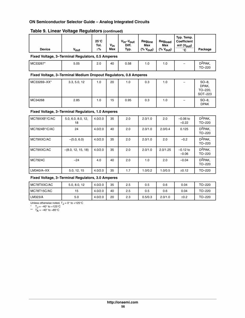
ON Semiconductor Selector Guide – Analog Integrated Circuits
http://onsemi.com 56
Table 9. Linear Voltage Regulators (continued)
Device Package
Typ. Temp.CoefficientmV (Vout)
°C
RegloadMax
(% Vout)
ReglineMax
(% Vout)
Vin–Vout Diff.Typ.
VinMax
25°CTol.±%Vout
Fixed Voltage, 3–Terminal Regulators, 0.5 Amperes
MC33267* 5.05 2.0 40 0.58 1.0 1.0 – D2PAK,TO–220
Fixed Voltage, 3–Terminal Medium Dropout Regulators, 0.8 Amperes
MC33269–XX* 3.3, 5.0, 12 1.0 20 1.0 0.3 1.0 – SO–8,DPAK,
TO–220,SOT–223
MC34268 2.85 1.0 15 0.95 0.3 1.0 – SO–8,DPAK
Fixed Voltage, 3–Terminal Regulators, 1.0 Amperes
MC78XXB*/C/AC 5.0, 6.0, 8.0, 12,18
4.0/2.0 35 2.0 2.0/1.0 2.0 –0.06 to–0.22
D2PAK,TO–220
MC7824B*/C/AC 24 4.0/2.0 40 2.0 2.0/1.0 2.0/0.4 0.125 D2PAK,TO–220
MC79XXC/AC –(5.0, 6.0) 4.0/2.0 35 2.0 2.0/1.0 2.0 –0.2 D2PAK,TO–220
MC79XXC/AC –(8.0, 12, 15, 18) 4.0/2.0 35 2.0 2.0/1.0 2.0/1.25 –0.12 to–0.06
D2PAK,TO–220
MC7924C –24 4.0 40 2.0 1.0 2.0 –0.04 D2PAK,TO–220
LM340/A–XX 5.0, 12, 15 4.0/2.0 35 1.7 1.0/0.2 1.0/0.5 ±0.12 TO–220
Fixed Voltage, 3–Terminal Regulators, 3.0 Amperes
MC78TXXC/AC 5.0, 8.0, 12 4.0/2.0 35 2.5 0.5 0.6 0.04 TO–220
MC78T15C/AC 15 4.0/2.0 40 2.5 0.5 0.6 0.04 TO–220
LM323/A 5.0 4.0/2.0 20 2.3 0.5/0.3 2.0/1.0 ±0.2 TO–220
Unless otherwise noted, TJ = 0° to +125°C* TJ = –40° to +125°C** TA = –40° to +85°C
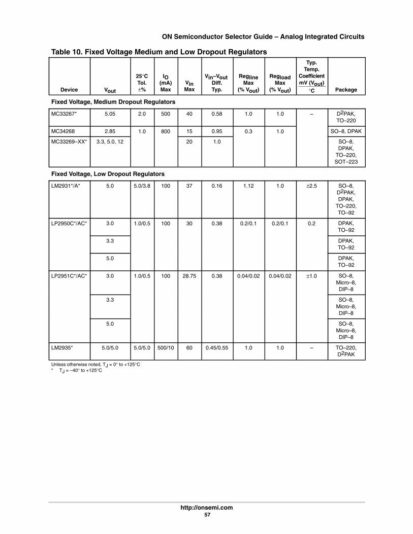
ON Semiconductor Selector Guide – Analog Integrated Circuits
http://onsemi.com 57
Table 10. Fixed Voltage Medium and Low Dropout Regulators
Device Vout
25°CTol.±%
IO(mA)Max
VinMax
Vin–Vout Diff.Typ.
ReglineMax
(% Vout)
RegloadMax
(% Vout)
Typ.Temp.
CoefficientmV (Vout)
°C Package
Fixed Voltage, Medium Dropout Regulators
MC33267* 5.05 2.0 500 40 0.58 1.0 1.0 – D2PAK,TO–220
MC34268 2.85 1.0 800 15 0.95 0.3 1.0 SO–8, DPAK
MC33269–XX* 3.3, 5.0, 12 20 1.0 SO–8,DPAK,
TO–220,SOT–223
Fixed Voltage, Low Dropout Regulators
LM2931*/A* 5.0 5.0/3.8 100 37 0.16 1.12 1.0 ±2.5 SO–8,D2PAK,DPAK,
TO–220,TO–92
LP2950C*/AC* 3.0 1.0/0.5 100 30 0.38 0.2/0.1 0.2/0.1 0.2 DPAK,TO–92
3.3 DPAK,TO–92
5.0 DPAK,TO–92
LP2951C*/AC* 3.0 1.0/0.5 100 28.75 0.38 0.04/0.02 0.04/0.02 ±1.0 SO–8,Micro–8,DIP–8
3.3 SO–8,Micro–8,DIP–8
5.0 SO–8,Micro–8,DIP–8
LM2935* 5.0/5.0 5.0/5.0 500/10 60 0.45/0.55 1.0 1.0 – TO–220,D2PAK
Unless otherwise noted, TJ = 0° to +125°C* TJ = –40° to +125°C
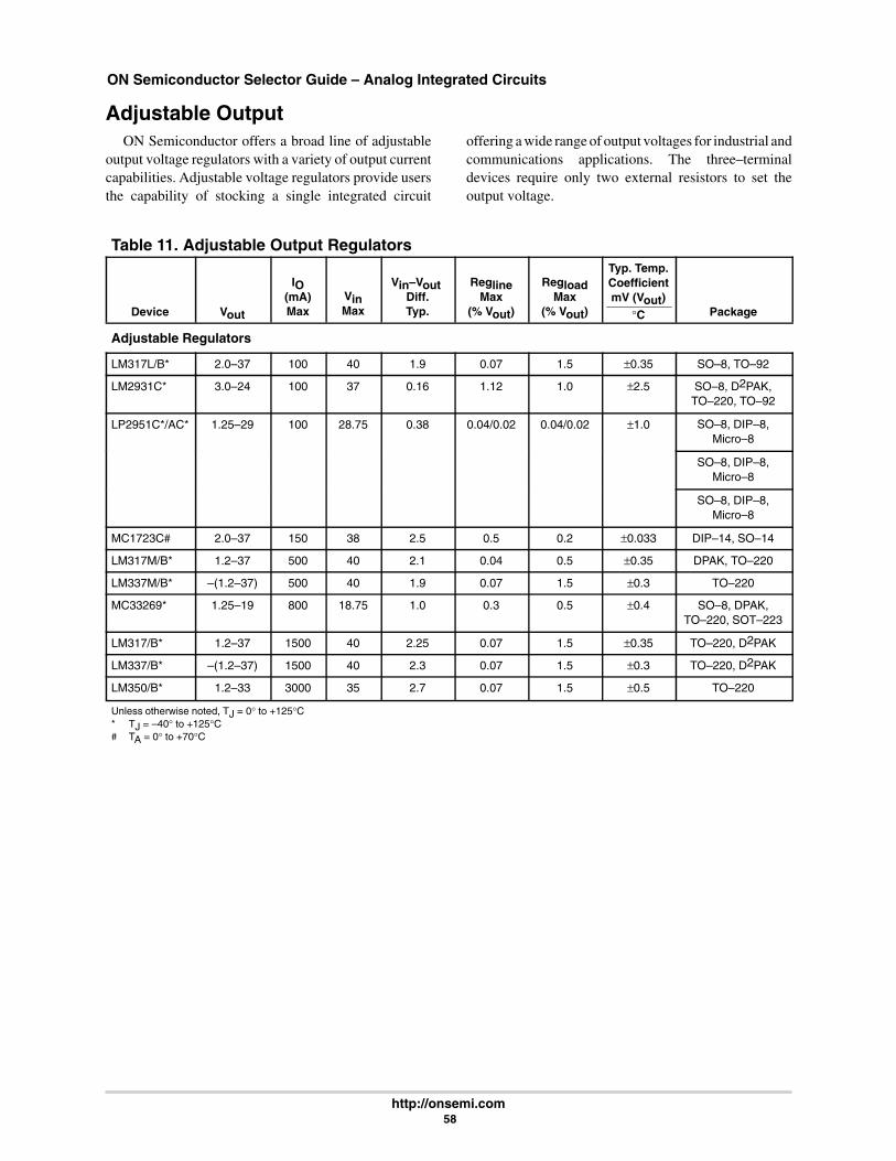
ON Semiconductor Selector Guide – Analog Integrated Circuits
http://onsemi.com 58
Adjustable OutputON Semiconductor offers a broad line of adjustable
output voltage regulators with a variety of output currentcapabilities. Adjustable voltage regulators provide usersthe capability of stocking a single integrated circuit
offering a wide range of output voltages for industrial andcommunications applications. The three–terminaldevices require only two external resistors to set theoutput voltage.
Table 11. Adjustable Output Regulators
Device Vout
IO(mA)Max
VinMax
Vin–Vout Diff.Typ.
ReglineMax
(% Vout)
RegloadMax
(% Vout)
Typ. Temp.CoefficientmV (Vout)
°C Package
Adjustable Regulators
LM317L/B* 2.0–37 100 40 1.9 0.07 1.5 ±0.35 SO–8, TO–92
LM2931C* 3.0–24 100 37 0.16 1.12 1.0 ±2.5 SO–8, D2PAK,TO–220, TO–92
LP2951C*/AC* 1.25–29 100 28.75 0.38 0.04/0.02 0.04/0.02 ±1.0 SO–8, DIP–8,Micro–8
SO–8, DIP–8,Micro–8
SO–8, DIP–8,Micro–8
MC1723C# 2.0–37 150 38 2.5 0.5 0.2 ±0.033 DIP–14, SO–14
LM317M/B* 1.2–37 500 40 2.1 0.04 0.5 ±0.35 DPAK, TO–220
LM337M/B* –(1.2–37) 500 40 1.9 0.07 1.5 ±0.3 TO–220
MC33269* 1.25–19 800 18.75 1.0 0.3 0.5 ±0.4 SO–8, DPAK,TO–220, SOT–223
LM317/B* 1.2–37 1500 40 2.25 0.07 1.5 ±0.35 TO–220, D2PAK
LM337/B* –(1.2–37) 1500 40 2.3 0.07 1.5 ±0.3 TO–220, D2PAK
LM350/B* 1.2–33 3000 35 2.7 0.07 1.5 ±0.5 TO–220
Unless otherwise noted, TJ = 0° to +125°C* TJ = –40° to +125°C# TA = 0° to +70°C

ON Semiconductor Selector Guide – Analog Integrated Circuits
http://onsemi.com 59
Micropower Voltage Regulators for PortableApplications80 mA Micropower Voltage RegulatorMC78LC00H, N
TA = –30° to +80°C, SOT–89, SOT–23 5 Leads
The MC78LC00 series voltage regulators arespecifically designed for use as a power source for videoinstruments, handheld communication equipment, andbattery powered equipment.
The MC78LC00 series features an ultra–low quiescentcurrent of 1.1 µA and a high accuracy output voltage. Eachdevice contains a voltage reference, an error amplifier, adriver transistor and resistors for setting the outputvoltage. These devices are available in either SOT–89, 3pin, or SOT–23, 5 pin, surface mount packages.
MC78LC00 Series Features:• Low Quiescent Current of 1.1 µA Typical
• Low Dropout Voltage (220 mV at 10 mA)
• Excellent Line Regulation (0.1%)
• High Accuracy Output Voltage (±2.5%)
• Wide Output Voltage Range (2.0 V to 6.0 V)
• Output Current for Low Power (up to 80 mA)
• Two Surface Mount Packages (SOT–89, 3 Pin, orSOT–23, 5 Pin)
ORDERING INFORMATION
DeviceOutputVoltage
OperatingTemperature
Range Package
MC78LC30HT1 3.0MC78LC33HT1 3.3
SOT–89MC78LC40HT1 4.0
SOT–89
MC78LC50HT1 5.0 TA = –30° toMC78LC30NTR 3.0
A+80°C
MC78LC33NTR 3.3SOT–23
MC78LC40NTR 4.0SOT–23
MC78LC50NTR 5.0
Other voltages from 2.0 to 6.0 V, in 0.1 V increments, are availableupon request. Consult factory for information.
2
Vin
1
Gnd
3
VO
Vref
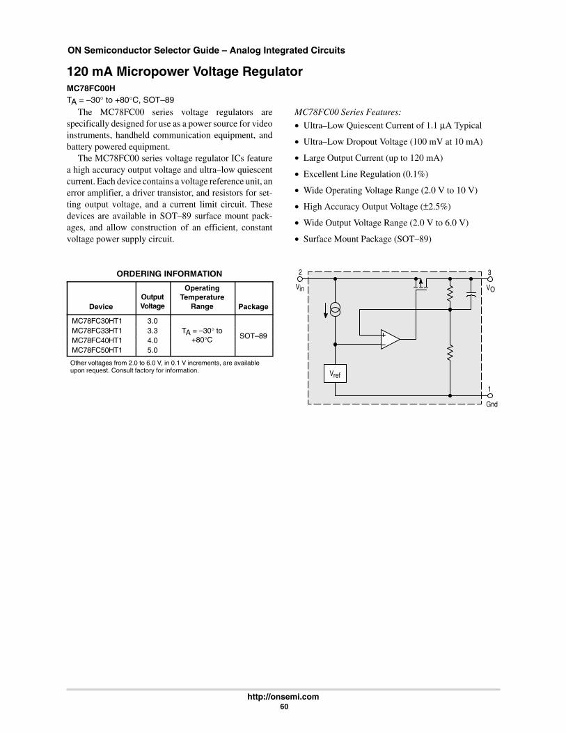
ON Semiconductor Selector Guide – Analog Integrated Circuits
http://onsemi.com 60
120 mA Micropower Voltage RegulatorMC78FC00HTA = –30° to +80°C, SOT–89
The MC78FC00 series voltage regulators arespecifically designed for use as a power source for videoinstruments, handheld communication equipment, andbattery powered equipment.
The MC78FC00 series voltage regulator ICs featurea high accuracy output voltage and ultra–low quiescentcurrent. Each device contains a voltage reference unit, anerror amplifier, a driver transistor, and resistors for set-ting output voltage, and a current limit circuit. Thesedevices are available in SOT–89 surface mount pack-ages, and allow construction of an efficient, constantvoltage power supply circuit.
MC78FC00 Series Features:
• Ultra–Low Quiescent Current of 1.1 µA Typical
• Ultra–Low Dropout Voltage (100 mV at 10 mA)
• Large Output Current (up to 120 mA)
• Excellent Line Regulation (0.1%)
• Wide Operating Voltage Range (2.0 V to 10 V)
• High Accuracy Output Voltage (±2.5%)
• Wide Output Voltage Range (2.0 V to 6.0 V)
• Surface Mount Package (SOT–89)
ORDERING INFORMATION
DeviceOutputVoltage
OperatingTemperature
Range Package
MC78FC30HT1 3.0MC78FC33HT1 3.3 TA = –30° to
SOT–89MC78FC40HT1 4.0 +80°C SOT–89
MC78FC50HT1 5.0
Other voltages from 2.0 to 6.0 V, in 0.1 V increments, are availableupon request. Consult factory for information.
2
Vin
1
Gnd
3
VO
Vref
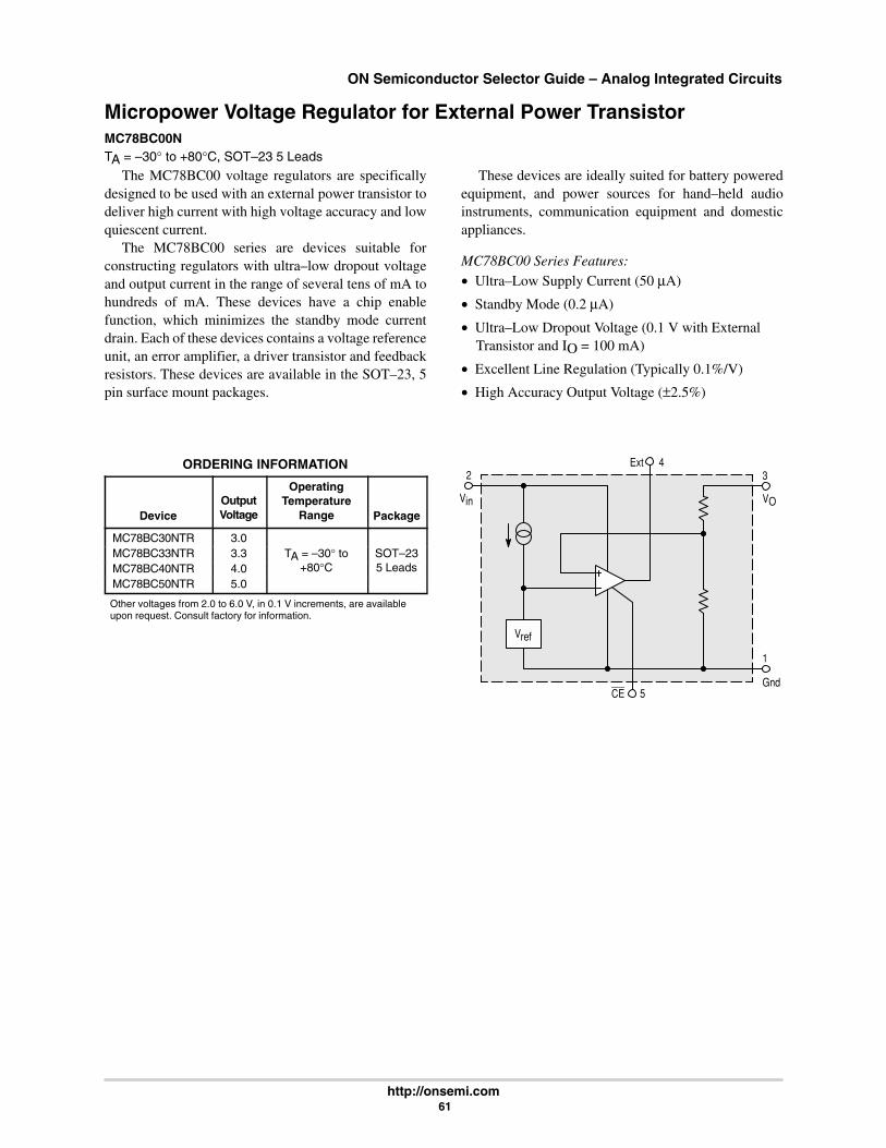
ON Semiconductor Selector Guide – Analog Integrated Circuits
http://onsemi.com 61
Micropower Voltage Regulator for External Power TransistorMC78BC00NTA = –30° to +80°C, SOT–23 5 Leads
The MC78BC00 voltage regulators are specificallydesigned to be used with an external power transistor todeliver high current with high voltage accuracy and lowquiescent current.
The MC78BC00 series are devices suitable forconstructing regulators with ultra–low dropout voltageand output current in the range of several tens of mA tohundreds of mA. These devices have a chip enablefunction, which minimizes the standby mode currentdrain. Each of these devices contains a voltage referenceunit, an error amplifier, a driver transistor and feedbackresistors. These devices are available in the SOT–23, 5pin surface mount packages.
These devices are ideally suited for battery poweredequipment, and power sources for hand–held audioinstruments, communication equipment and domesticappliances.
MC78BC00 Series Features:
• Ultra–Low Supply Current (50 µA)
• Standby Mode (0.2 µA)
• Ultra–Low Dropout Voltage (0.1 V with ExternalTransistor and IO = 100 mA)
• Excellent Line Regulation (Typically 0.1%/V)
• High Accuracy Output Voltage (±2.5%)
ORDERING INFORMATION
DeviceOutputVoltage
OperatingTemperature
Range Package
MC78BC30NTR 3.0MC78BC33NTR 3.3 TA = –30° to SOT–23MC78BC40NTR 4.0 +80°C 5 LeadsMC78BC50NTR 5.0
Other voltages from 2.0 to 6.0 V, in 0.1 V increments, are availableupon request. Consult factory for information.
2
Vin
1
Gnd
3
VO
4Ext
5CE
Vref

ON Semiconductor Selector Guide – Analog Integrated Circuits
http://onsemi.com 62
Micropower Voltage Regulators for Portable Applications (continued)
Low Noise 150 mA Low Drop Out (LDO) Linear Voltage RegulatorMC78PC00
TA = –40° to +85°C, SOT–23 5 Lead Package
The MC78PC00 are a series of CMOS linear voltageregulators with high output voltage accuracy, low supplycurrent, low dropout voltage, and high Ripple Rejection.Each of these voltage regulators consists of an internalvoltage reference, an error amplifier, resistors, a currentlimiting circuit and a chip enable circuit.
The dynamic Response to line and load is fast, whichmakes these products ideally suited for use in hand–heldcommunication equipment.
The MC78PC00 series are housed in the SOT–23 5lead package, for maximum board space saving.
MC78PC00 Series Features:• Ultra–Low Supply Current: typical 35 A in ON
mode with no load
• Standby Mode: typical 0.1 A
• Low Dropout Voltage: typical 0.2 V @ IOUT =100 mA
• High Ripple Rejection: typical 70 dB @ f = 1 kHz
• Low Temperature–Drift Coefficient of OutputVoltage: typical ±100 ppm/°C
• Excellent Line Regulation: typical 0.05%/V
• High Accuracy Output Voltage: ±2.0%
• Fast Dynamic Response to Line and Load
• Small Package: SOT–23 5 leads
• Built–in Chip Enable circuit (CE input pin)
• Similar Pinout to the LP2980/1/2 and MIC5205
ORDERING INFORMATION
DeviceOperating
Temperature Range Package
MC78PC28NTRMC78PC30NTR
TA = –40° to +85°CSOT–23
MC78PC33NTRTA = –40° to +85°C 5 Leads
MC78PC50NTR
Other voltages are available. Consult your ON Semiconductorrepresentative.
Block Diagram
1VIN
5VOUT
Vref
CE3 2
GND
CURRENT LIMIT
MC78PCxx
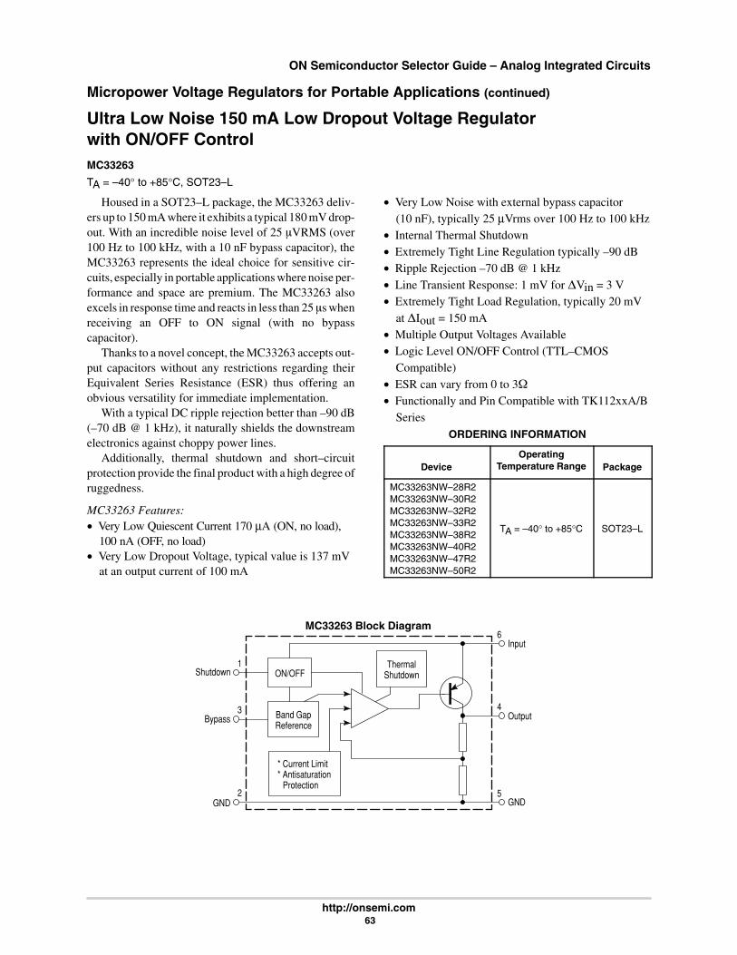
ON Semiconductor Selector Guide – Analog Integrated Circuits
http://onsemi.com 63
Micropower Voltage Regulators for Portable Applications (continued)
Ultra Low Noise 150 mA Low Dropout Voltage Regulatorwith ON/OFF ControlMC33263
TA = –40° to +85°C, SOT23–L
Housed in a SOT23–L package, the MC33263 deliv-ers up to 150 mA where it exhibits a typical 180 mV drop-out. With an incredible noise level of 25 VRMS (over100 Hz to 100 kHz, with a 10 nF bypass capacitor), theMC33263 represents the ideal choice for sensitive cir-cuits, especially in portable applications where noise per-formance and space are premium. The MC33263 alsoexcels in response time and reacts in less than 25 s whenreceiving an OFF to ON signal (with no bypasscapacitor).
Thanks to a novel concept, the MC33263 accepts out-put capacitors without any restrictions regarding theirEquivalent Series Resistance (ESR) thus offering anobvious versatility for immediate implementation.
With a typical DC ripple rejection better than –90 dB(–70 dB @ 1 kHz), it naturally shields the downstreamelectronics against choppy power lines.
Additionally, thermal shutdown and short–circuitprotection provide the final product with a high degree ofruggedness.
MC33263 Features:• Very Low Quiescent Current 170 µA (ON, no load),
100 nA (OFF, no load)• Very Low Dropout Voltage, typical value is 137 mV
at an output current of 100 mA
• Very Low Noise with external bypass capacitor(10 nF), typically 25 µVrms over 100 Hz to 100 kHz
• Internal Thermal Shutdown• Extremely Tight Line Regulation typically –90 dB• Ripple Rejection –70 dB @ 1 kHz• Line Transient Response: 1 mV for Vin = 3 V• Extremely Tight Load Regulation, typically 20 mV
at Iout = 150 mA• Multiple Output Voltages Available• Logic Level ON/OFF Control (TTL–CMOS
Compatible)• ESR can vary from 0 to 3• Functionally and Pin Compatible with TK112xxA/B
SeriesORDERING INFORMATION
DeviceOperating
Temperature Range Package
MC33263NW–28R2MC33263NW–30R2MC33263NW–32R2MC33263NW–33R2MC33263NW–38R2MC33263NW–40R2MC33263NW–47R2MC33263NW–50R2
TA = –40° to +85°C SOT23–L
GND
MC33263 Block Diagram
* Current Limit* Antisaturation* Protection
Input
Output
GND
Bypass3
2
6
4
5
Band GapReference
ON/OFFShutdown1 Thermal
Shutdown
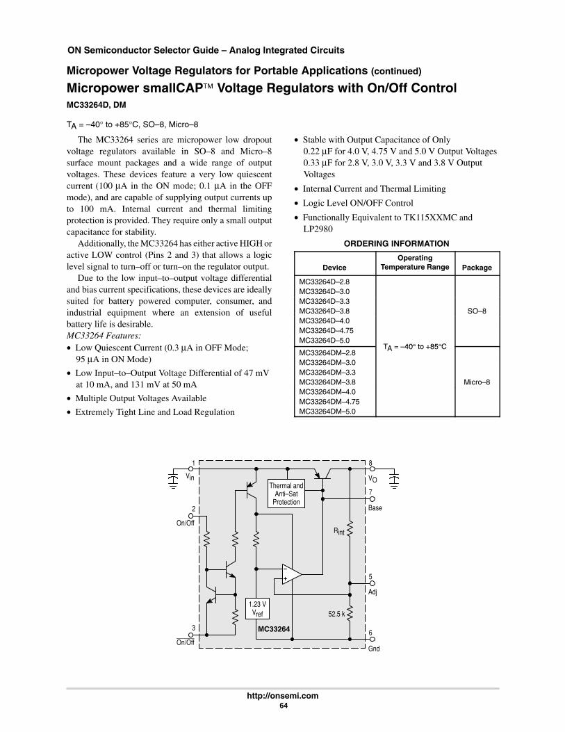
ON Semiconductor Selector Guide – Analog Integrated Circuits
http://onsemi.com 64
Micropower Voltage Regulators for Portable Applications (continued)
Micropower smallCAP Voltage Regulators with On/Off ControlMC33264D, DM
TA = –40° to +85°C, SO–8, Micro–8
The MC33264 series are micropower low dropoutvoltage regulators available in SO–8 and Micro–8surface mount packages and a wide range of outputvoltages. These devices feature a very low quiescentcurrent (100 µA in the ON mode; 0.1 µA in the OFFmode), and are capable of supplying output currents upto 100 mA. Internal current and thermal limitingprotection is provided. They require only a small outputcapacitance for stability.
Additionally, the MC33264 has either active HIGH oractive LOW control (Pins 2 and 3) that allows a logiclevel signal to turn–off or turn–on the regulator output.
Due to the low input–to–output voltage differentialand bias current specifications, these devices are ideallysuited for battery powered computer, consumer, andindustrial equipment where an extension of usefulbattery life is desirable.MC33264 Features:• Low Quiescent Current (0.3 µA in OFF Mode;
95 µA in ON Mode)
• Low Input–to–Output Voltage Differential of 47 mVat 10 mA, and 131 mV at 50 mA
• Multiple Output Voltages Available
• Extremely Tight Line and Load Regulation
• Stable with Output Capacitance of Only0.22 µF for 4.0 V, 4.75 V and 5.0 V Output Voltages0.33 µF for 2.8 V, 3.0 V, 3.3 V and 3.8 V OutputVoltages
• Internal Current and Thermal Limiting
• Logic Level ON/OFF Control
• Functionally Equivalent to TK115XXMC andLP2980
ORDERING INFORMATION
DeviceOperating
Temperature Range Package
MC33264D–2.8MC33264D–3.0MC33264D–3.3MC33264D–3.8 SO–8MC33264D–4.0MC33264D–4.75MC33264D–5.0
TA = 40° to +85°CMC33264DM–2.8
TA = –40° to +85°C
MC33264DM–3.0MC33264DM–3.3MC33264DM–3.8 Micro–8MC33264DM–4.0MC33264DM–4.75MC33264DM–5.0
On/Off
Thermal andAnti–Sat
Protection
1.23 VVref
VO
Base
Adj
Gnd
Vin
On/Off
1
2
3
8
7
6
5
MC33264
52.5 k
Rint

ON Semiconductor Selector Guide – Analog Integrated Circuits
http://onsemi.com 65
Micropower Voltage Regulators for Portable Applications (continued)
5A Low Dropout Fast Response Positive Adjustableand Fixed Voltage RegulatorsLT1585A
TA = 0° to 125°C, TO–220, D2PAK
The LT1585A is a low dropout 3–terminal voltageregulator with 5A output current capability.
Design has been optimized for low voltage applica-tions where transient response and minimum input volt-age are critical. This voltage regulator features a lowdropout voltage and fast transient response. Theseimprovements make them ideal for low voltage micro-processor applications requiring a regulated 2.5V to 3.6Voutput with an input supply below 7V.
Current limits is trimmed to ensure specified outputcurrent and controlled short–circuit current. On–chipthermal limiting provides protection against any com-
bination of overload that would create excessive junctiontemperatures. The LT1585A is available in the industrystandard 3–pin TO–220 and D2PAK power package.
LT1585A Features:• Fast Transient Response
• Guaranteed Dropout Voltage at Multiple Currents
• Load Regulation: 0.05% Typ
• Trimmed Current Limit
• On–Chip Thermal Limiting
• Standard 3–Pin Power Package
ORDERING INFORMATION
DeviceOperating
Temperature Range Package
LT1585ACT TO–220
LT1585ACMTA = 0° to 125°C
D2PAK
LT1585ACT–1.5TA = 0° to 125°C
TO–220
LT1585ACM–1.5 D2PAK
Simplified Block DiagramVin
Vout
+
–
ThermalLimit
Adjust
ON Semiconductor Selector Guide – Analog Integrated Circuits
http://onsemi.com 66
Special Voltage RegulatorsTable 12. Voltage Regulators
F nction Feat res Package DeviceFunction Features Package Device
Multifunction VeryLow Dropout VoltageRegulator
A monolithic integrated 5.0 V voltage regulator with a very low drop-out and additional functions such as power–on reset and input volt-age sense. It is designed for supplying the micro–computer con-trolled systems especially in automotive applications.
DIP–8, SO–8 L4949
Low Dropout VoltageRegulator
Fixed and adjustable positive output voltage regulators whichmaintain regulation with very low input–to–output voltage differential.
TO–92, TO–220,DPAK, D2PAK, SO–8
LM2931Series
Low Dropout VoltageRegulator
Low voltage differential regulator featuring dual positive 5.0 Voutputs; switched currents in excess of 750 mA and 10 mA standbycurrent. Fixed quiescent current is less than 3.0 mA.
TO–220, D2PAK LM2935
Low Dropout VoltageRegulator
Positive 5.0 V, 500 mA regulator with on–chip power–up–resetcircuit with externally programmable delay, current limit, and thermalshutdown.
TO–220, D2PAK MC33267
Low Dropout VoltageRegulator
Positive 3.3 V, 5.0 V, 12 V, 800 mA regulator. SO–8, DPAK,SOT–223, TO–220
MC33269
Low Dropout VoltageRegulator
Positive regulator with 5 outputs fixed 2.8 V and 13 V. TSSOP–16 MC33765
Special RegulatorsVoltage Regulator/SupervisoryTable 13. Voltage Regulator/Supervisory
Vout(V) IO
(mA)
Vin(V)
Regline Regload TA Suffix/Device Min Max
(mA)Max Min Max
Regline(mV) Max
Regload(mV) Max
TA(°C)
Suffix/Package
MC34160 4.75 5.25 100 7.0 40 40 50 0 to +70 DIP–16,SO 16LMC33160 –40 to +85SO–16L
MC33267 4.9 5.2 500 6.0 26 50 50 –40 to +105 TO–220,D2PAK
* These ICs are intended for powering cellular phone GaAs power amplifiers and can be used for other portable applications as well.

ON Semiconductor Selector Guide – Analog Integrated Circuits
http://onsemi.com 67
Voltage Regulator/Supervisory (continued)
Microprocessor Voltage Regulator and Supervisory CircuitMC34160P, DW
TA = 0° to +70°C, DIP–16, SO–16L
MC33160P, DW
TA = –40° to +85°C, DIP–16, SO–16L
The MC34160 series is a voltage regulator and supervi-sory circuit containing many of the necessary monitoringfunctions required in microprocessor based systems. It isspecifically designed for appliance and industrial applica-tions offering the designer a cost effective solution withminimal external components. These integrated circuitsfeature a 5.0 V, 100 mA regulator with short circuit currentlimiting, pinned out 2.6 V bandgap reference, low voltage
reset comparator, power warning comparator with pro-grammable hysteresis, and an uncommitted comparatorideally suited for microprocessor line synchronization.
Additional features include a chip disable input for lowstandby current, and internal thermal shutdown for overtemperature protection.
These devices are contained in a 16 pin dual–in–lineheat tab plastic package for improved thermal conduction.
VCC
ChipDisable
PowerSense
HysteresisAdjust
NoninvertingInput
InvertingInput
14
15
9
10
2
1
RegulatorOutput
Reset
PowerWarning
ReferenceOutput
ComparatorOutput
Gnd 4, 5,12, 13
2.6 VReference
0.01R
0.913R
R
IHIH “On”/“Off”
6
8
16
7
11ThermalShutdown
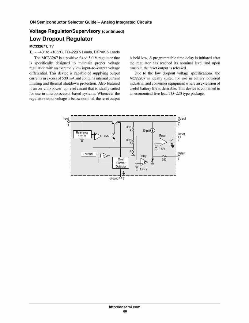
ON Semiconductor Selector Guide – Analog Integrated Circuits
http://onsemi.com 68
Voltage Regulator/Supervisory (continued)
Low Dropout RegulatorMC33267T, TV
TJ = –40° to +105°C, TO–220 5 Leads, D2PAK 5 Leads
The MC33267 is a positive fixed 5.0 V regulator thatis specifically designed to maintain proper voltageregulation with an extremely low input–to–output voltagedifferential. This device is capable of supplying outputcurrents in excess of 500 mA and contains internal currentlimiting and thermal shutdown protection. Also featuredis an on–chip power–up reset circuit that is ideally suitedfor use in microprocessor based systems. Whenever theregulator output voltage is below nominal, the reset output
is held low. A programmable time delay is initiated afterthe regulator has reached its nominal level and upontimeout, the reset output is released.
Due to the low dropout voltage specifications, theMC33267 is ideally suited for use in battery poweredindustrial and consumer equipment where an extension ofuseful battery life is desirable. This device is contained inan economical five lead TO–220 type package.
Input Output
1 5
Reference1.25 V
Thermal
OverCurrentDetector
Ground 3
1.25 V
DelayR
0.03R
3.01R 20 µA
3.8 V
Reset
200
Reset
2
Delay
4+
+
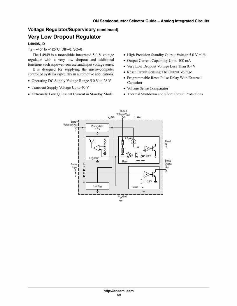
ON Semiconductor Selector Guide – Analog Integrated Circuits
http://onsemi.com 69
Voltage Regulator/Supervisory (continued)
Very Low Dropout RegulatorL4949N, D
TJ = –40° to +125°C, DIP–8, SO–8
The L4949 is a monolithic integrated 5.0 V voltageregulator with a very low dropout and additionalfunctions such as power–on reset and input voltage sense.
It is designed for supplying the micro–computercontrolled systems especially in automotive applications.
• Operating DC Supply Voltage Range 5.0 V to 28 V
• Transient Supply Voltage Up to 40 V
• Extremely Low Quiescent Current in Standby Mode
• High Precision Standby Output Voltage 5.0 V ±1%
• Output Current Capability Up to 100 mA
• Very Low Dropout Voltage Less Than 0.4 V
• Reset Circuit Sensing The Output Voltage
• Programmable Reset Pulse Delay With ExternalCapacitor
• Voltage Sense Comparator
• Thermal Shutdown and Short Circuit Protections
Regulator
1.23 Vref
2.0 V
2.0 µA
Reset
1.23 V
Sense
Gnd
SenseOutput(So)
Reset
SenseInput
(Si)
SupplyVoltage (VCC)
VZ
OutputVoltage (Vout)
CT3 8 4
6
7
5
2
1
Vs
+
–
+
–
Preregulator6.0 V

ON Semiconductor Selector Guide – Analog Integrated Circuits
http://onsemi.com 70
Voltage Regulator/Supervisory (continued)
Very Low Dropout/Ultra Noise 5 Outputs Voltage RegulatorMC33765TA = 40° to +85°C, TSSOP16
The MC33765 is an ultra low noise, very low dropoutvoltage regulator with five independent outputs which isavailable in TSSOP 16 surface mount package.
Two versions are available: 2.8 V or 3.0 V. The voltageof all five outputs is 2.8 V or 3.0 V typical but each outputis capable of supplying different currents up to 150 mAfor output 4. The device features a very low dropout volt-age (0.11 V typical for maximum output current), verylow quiescent current (5.0 mA maximum in OFF mode,130 mA typical in ON mode) and one of the output (out-put 3) exhibits a very low noise level which allows thedriving of noise sensitive circuitry. Internal current andthermal limiting protections are provided.
Additionally, the MC33765 has an independentEnable input pin for each output. It includes also a com-mon Enable pin to shutdown the complete circuit whennot used. The Common Enable pin has the highest prior-ity over the five independent Enable input pins.
The voltage regulators VR1, VR2 and VR3 have acommon input voltage pin VCC1.
The other voltage regulators VR4 and VR5 have acommon input voltage pin VCC2.
MC33765 Features:• Five Independent Outputs at 2.8 V or 3.0 V Typical• Internal Trimmed Voltage Reference• Vout Tolerance ±3.0% at 25°C• Enable Input Pin (Logic–Controlled Shutdown) for
Each of the Five Outputs• Common Enable Pin to Shutdown the Whole Circuit• Very Low Dropout Voltage (0.11 V Typical for
Output 1, 2, 3 and 5; 0.17 V Typical for Output 4 atMaximum Current)
• Very Low Quiescent Current (Maximum 5.0 µA inOFF Mode, 130 µA Typical in ON Mode)
• Ultra Low Noise for VR3 (30 µV RMS Max,100 Hz < f < 100 kHz)
• Internal Current and Thermal Limit• 100 nF for VR1, VR2, VR4 and VR5 and 1.0 µF for
VR3 for Stability• Supply Voltage Rejection: 60 dB (Typical) @
f = 1.0 kHz
ORDERING INFORMATION
Device Voltage VersionOperating
Temperature Range Package
MC33765DTB, R2MC33765DTB–30, R2
2.8 V Fixed3.0 V Fixed
TA = 40° to +85°C TSSOP–16
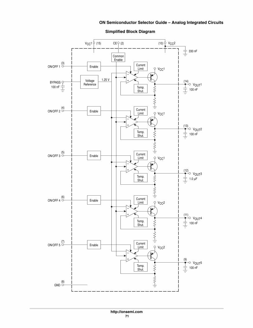
ON Semiconductor Selector Guide – Analog Integrated Circuits
http://onsemi.com 71
Enable CurrentLimit
Temp.Shut.
Enable CurrentLimit
Temp.Shut.
Enable CurrentLimit
Temp.Shut.
Enable CurrentLimit
Temp.Shut.
Enable CurrentLimit
Temp.Shut.
CommonEnable
+
–
+
–
+
–
+
–
+
–
Simplified Block Diagram
330 nF
VOUT1
VCC2
(14)
100 nF
VOUT2(13)
100 nF
VOUT3(12)
1.0 F
VOUT4(11)
100 nF
VOUT5(9)
100 nF
VCC1
VCC1
VCC1
VCC2
VCC2
(8)GND
(7)ON/OFF 5
(6)ON/OFF 4
(5)ON/OFF 3
VCC1
(4)ON/OFF 2
BYPASS
(3)ON/OFF 1
VoltageReference
1.25 V
(15) (2)CE
100 nF
(10)
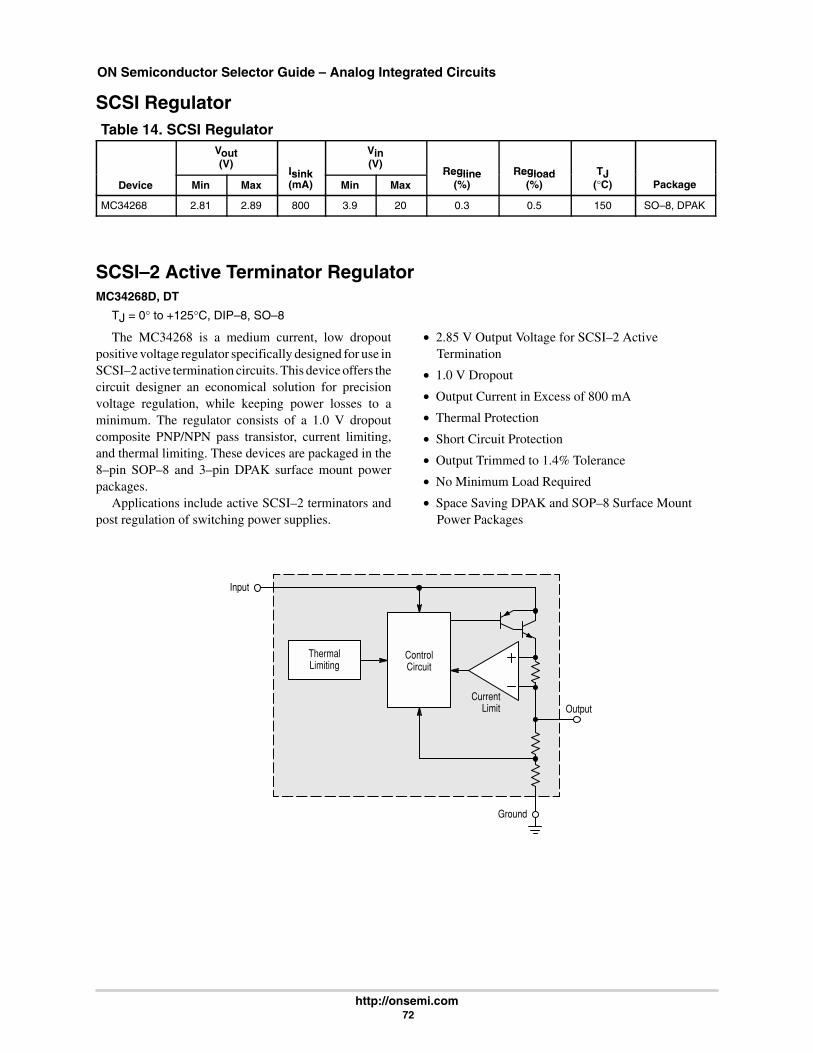
ON Semiconductor Selector Guide – Analog Integrated Circuits
http://onsemi.com 72
SCSI RegulatorTable 14. SCSI Regulator
Vout(V)
Isink
Vin(V)
Regline Regload TJDevice Min Max
Isink(mA) Min Max
Regline(%)
Regload(%)
TJ(°C) Package
MC34268 2.81 2.89 800 3.9 20 0.3 0.5 150 SO–8, DPAK
SCSI–2 Active Terminator RegulatorMC34268D, DT
TJ = 0° to +125°C, DIP–8, SO–8
The MC34268 is a medium current, low dropoutpositive voltage regulator specifically designed for use inSCSI–2 active termination circuits. This device offers thecircuit designer an economical solution for precisionvoltage regulation, while keeping power losses to aminimum. The regulator consists of a 1.0 V dropoutcomposite PNP/NPN pass transistor, current limiting,and thermal limiting. These devices are packaged in the8–pin SOP–8 and 3–pin DPAK surface mount powerpackages.
Applications include active SCSI–2 terminators andpost regulation of switching power supplies.
• 2.85 V Output Voltage for SCSI–2 ActiveTermination
• 1.0 V Dropout
• Output Current in Excess of 800 mA
• Thermal Protection
• Short Circuit Protection
• Output Trimmed to 1.4% Tolerance
• No Minimum Load Required
• Space Saving DPAK and SOP–8 Surface MountPower Packages
Input
ThermalLimiting
ControlCircuit
CurrentLimit Output
Ground
ANALOG INTEGRATED CIRCUITS
SIGNALCONDITIONING
BATTERYMANAGEMENT
POWERMANAGEMENT
SYSTEMMANAGEMENT
MOTORCONTROL INTERFACE OTHER
CIRCUITS
Op–Amps
Comparators
LithiumBattery
ProtectionICs
ChargeControllers
DC–DCConverters
with Inductor
Off–LineSMPS
Controllers
UndervoltageSupervisory
OvervoltageSupervisory
DataTransmission
DisplayDrivers
Timers
Linear Four–QuadrantMultiplier
Power FactorControllers
VoltageReferences
Linear VoltageRegulators
LDO LinearVoltage
Regulators
MOSFET/IGBT Drivers
DedicatedDrivers
Dedicated PowerMgmnt Controllers
DC MotorControl
ON Semiconductor Selector Guide – Analog Integrated Circuits
http://onsemi.com 73
MOSFET/IGBT Drivers
In Brief . . .The most important design aspect of a MOSFET/IGBT
gate drive is optimization of the switching characteristics.The switching characteristics are especially important inmotor control applications in which PWM transistors areused in a bridge configuration. In these applications, thegate drive circuit components should be selected to opti-mize turn–on, turn–off and off–state impedance.
Page
High Speed Dual Drivers 74. . . . . . . . . . . . . . . . . . . . . . . Single IGBT Driver 75. . . . . . . . . . . . . . . . . . . . . . . . . . . .
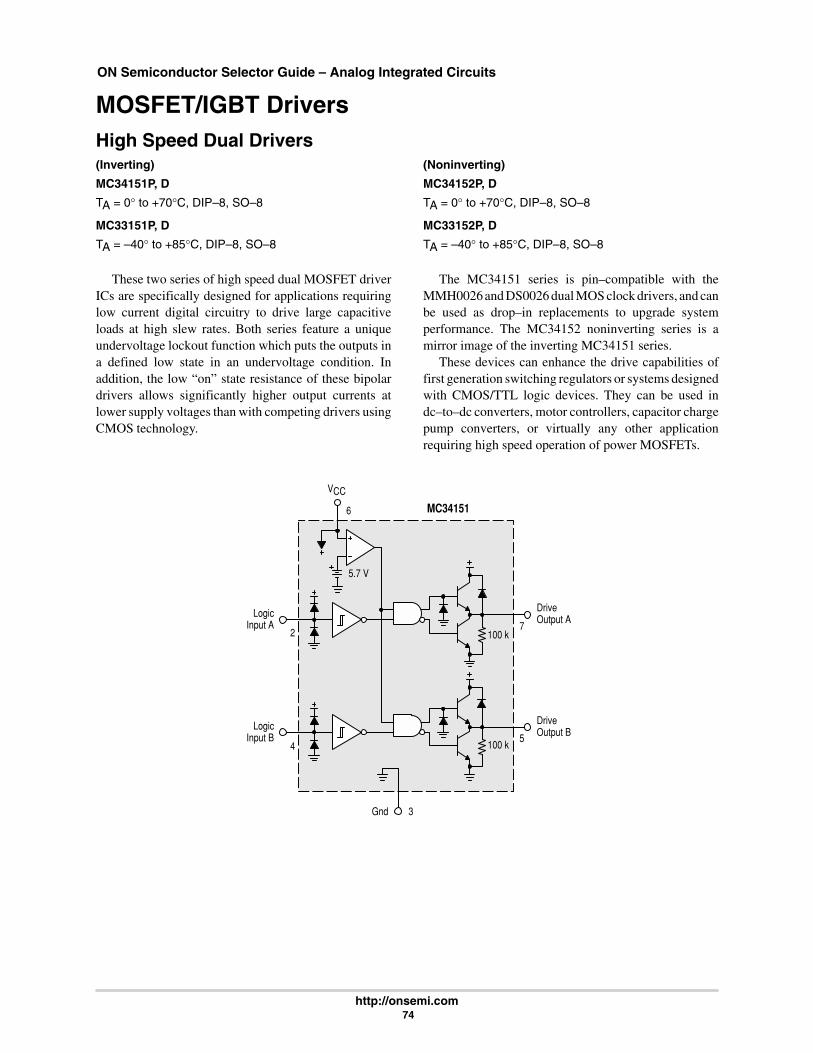
ON Semiconductor Selector Guide – Analog Integrated Circuits
http://onsemi.com 74
MOSFET/IGBT DriversHigh Speed Dual Drivers(Inverting)
MC34151P, D
TA = 0° to +70°C, DIP–8, SO–8
MC33151P, D
TA = –40° to +85°C, DIP–8, SO–8
(Noninverting)
MC34152P, D
TA = 0° to +70°C, DIP–8, SO–8
MC33152P, D
TA = –40° to +85°C, DIP–8, SO–8
These two series of high speed dual MOSFET driverICs are specifically designed for applications requiringlow current digital circuitry to drive large capacitiveloads at high slew rates. Both series feature a uniqueundervoltage lockout function which puts the outputs ina defined low state in an undervoltage condition. Inaddition, the low “on” state resistance of these bipolardrivers allows significantly higher output currents atlower supply voltages than with competing drivers usingCMOS technology.
The MC34151 series is pin–compatible with theMMH0026 and DS0026 dual MOS clock drivers, and canbe used as drop–in replacements to upgrade systemperformance. The MC34152 noninverting series is amirror image of the inverting MC34151 series.
These devices can enhance the drive capabilities offirst generation switching regulators or systems designedwith CMOS/TTL logic devices. They can be used indc–to–dc converters, motor controllers, capacitor chargepump converters, or virtually any other applicationrequiring high speed operation of power MOSFETs.
MC34151
3
LogicInput A
LogicInput B
2
4
Gnd
DriveOutput A
DriveOutput B
5
7
6
100 k
100 k
5.7 V
VCC

ON Semiconductor Selector Guide – Analog Integrated Circuits
http://onsemi.com 75
MOSFET/IGBT Drivers (continued)
Single IGBT DriverMC33153P, D
TA = –40° to +105°C, DIP–8, SO–8
The MC33153 is specifically designed to drive thegate of an IGBT used for ac induction motors. It can beused with discrete IGBTs and IBGT modules up to 100 A.
Typical applications are ac induction motor control,brushless dc motor control, and uninterruptable powersupplies.
These devices are available in dual–in–line andsurface mount packages and include the followingfeatures:
• High Current Output Stage : 1.0 A Source – 2.0 ASink
• Protection Circuits for Both Conventional andSenseIGBTs
• Current Source for Blanking Timing• Protection Against Overcurrent and Short Circuit• Undervoltage Lockout Optimized for IGBT’s• Negative Gate Drive Capability
CurrentSenseInput1
2
KelvinGnd
8
BlankingDesatur–ation
5
GateDriveOuptut
7
4
3
6VCC
VEE
Input
Output
VCC
VEE
VCC
Desat./Blank.Comparator
OvercurrentComparator
Over–currentLatch
SRQ
VCC
VEE
VCC
VEE
VCC
VEE
VEE VEE
VCC
VCC
Short CircuitComparator
SRQ
ANALOG INTEGRATED CIRCUITS
SIGNALCONDITIONING
BATTERYMANAGEMENT
POWERMANAGEMENT
SYSTEMMANAGEMENT
MOTORCONTROL INTERFACE OTHER
CIRCUITS
Op–Amps
Comparators
LithiumBattery
ProtectionICs
ChargeControllers
DC–DCConverters
with Inductor
Off–LineSMPS
Controllers
UndervoltageSupervisory
OvervoltageSupervisory
DataTransmission
DisplayDrivers
Timers
Linear Four–QuadrantMultiplier
Power FactorControllers
VoltageReferences
Linear VoltageRegulators
LDO LinearVoltage
Regulators
MOSFET/IGBT Drivers
DedicatedDrivers
Dedicated PowerMgmnt Controllers
DC MotorControl
ON Semiconductor Selector Guide – Analog Integrated Circuits
http://onsemi.com 76
Dedicated Drivers
In Brief . . .Dedicated drivers are designed and developed for spe-
cific application like electronic ballast. These drivers aredesigned to meet the specific application requirements.Therefore the overall system performance as well as costis highly maintained and minimized respectively. Ulti-mately the uses of these devices require a simpler systemdesign.
PageHalf Bridge Controller and Driverfor Industrial Linear Tubes 77. . . . . . . . . . . . . . . . . . . . .
Power Controllers 78. . . . . . . . . . . . . . . . . . . . . . . . . . . . . Zero Voltage Switch 78. . . . . . . . . . . . . . . . . . . . . . . . . Zero Voltage Controller 79. . . . . . . . . . . . . . . . . . . . . .

ON Semiconductor Selector Guide – Analog Integrated Circuits
http://onsemi.com 77
Half Bridge Controller and Driver for Industrial Linear TubesMC33157DW
The MC33157DW includes the oscillator circuit andtwo output channels to control a half–bridge power stage.One of the channels is ground–referenced. The secondone is floating to provide a bootstrap operation for thehigh side switch.
Dedicated Driver for Industrial Linear Tubes
• Main oscillator is current controlled, making it easyto set up by a single external resistor. On top of that,such a feature is useful to implement a dimmingfunction by frequency shift.
• Filament preheating time control built–in.• The strike sequence is controllable by external
passive components, the resonant frequency beingindependently adjustable. This frequency can bemade different from the preheating and the steadystate values. A frequency sweep between two
defined values makes this IC suitable for any serieresonant topologies.
• Dedicated internal comparator provides an easylamp strike detection implementation.
• Digital RESET pin provides a fast reset of thesystem (less than 10 µs). Both output Mosfet are setto “OFF’’ state when RESET is zero.
• Adjustable dead time makes the product suitable forany snubber capacitor and size of MOSFET used aspower switches.
• Designed to be used with standard setting capacitors470 nF.
• A voltage reference, derived from the internalbandgap, is provided for external usage. Thisvoltage is 100% trimmed at probe level yielding a2% tolerance over the temperature range.
ORDERING INFORMATION
DeviceTested Operating
Temperature Range Package
MC33157DW TA = –40° to +85°C Plastic SO–16L
HIGH SIDEBUFFER
LOW SIDEBUFFER
161514131211
VHSVHOVOUTNC
VLOGND
LEVELSHIFTER
ENABLEDead Time
CONTROL LOGIC
STRIKE detection
ClearINHIBIT
CO
MPA
RAT
OR
R
R
R
+Vref
Iop
+Vref
IphIfstrike
+Vref2ICO
7
ROP
6
COPCPH
3
Iph
PREHEAT & STRIKE CONTROL
CSWEEP
54
RPHREN
D S
WP
+Vref
UULO
BAND GAPREFERENCE
15 V
VDD
1
+Vref(+7 V)
DT adjust8
StrikeDetection
9
10RESET
Latch
Q
CVth
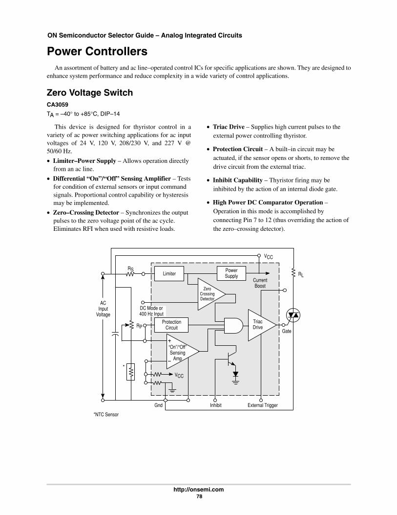
ON Semiconductor Selector Guide – Analog Integrated Circuits
http://onsemi.com 78
Power ControllersAn assortment of battery and ac line–operated control ICs for specific applications are shown. They are designed to
enhance system performance and reduce complexity in a wide variety of control applications.
Zero Voltage SwitchCA3059
TA = –40° to +85°C, DIP–14
This device is designed for thyristor control in avariety of ac power switching applications for ac inputvoltages of 24 V, 120 V, 208/230 V, and 227 V @50/60 Hz.
• Limiter–Power Supply – Allows operation directlyfrom an ac line.
• Differential “On”/“Off” Sensing Amplifier – Testsfor condition of external sensors or input commandsignals. Proportional control capability or hysteresismay be implemented.
• Zero–Crossing Detector – Synchronizes the outputpulses to the zero voltage point of the ac cycle.Eliminates RFI when used with resistive loads.
• Triac Drive – Supplies high current pulses to theexternal power controlling thyristor.
• Protection Circuit – A built–in circuit may beactuated, if the sensor opens or shorts, to remove thedrive circuit from the external triac.
• Inhibit Capability – Thyristor firing may beinhibited by the action of an internal diode gate.
• High Power DC Comparator Operation –Operation in this mode is accomplished byconnecting Pin 7 to 12 (thus overriding the action ofthe zero–crossing detector).
DC Mode or400 Hz Input
CurrentBoost
PowerSupply
ACInput
Voltage
VCC
RSRL
TriacDrive
Limiter
VCC
RPGate
Gnd
*NTC Sensor
Inhibit External Trigger
*
“On”/“Off”Sensing
Amp
ProtectionCircuit
ZeroCrossingDetector
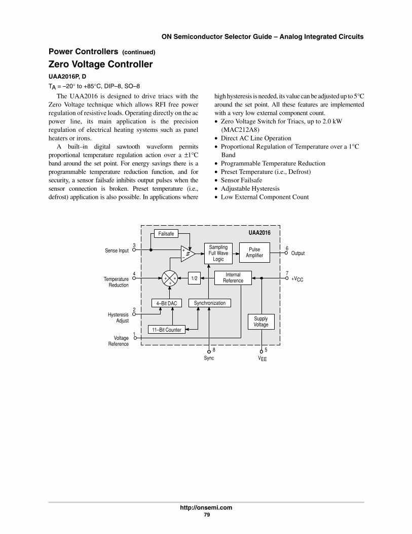
ON Semiconductor Selector Guide – Analog Integrated Circuits
http://onsemi.com 79
Power Controllers (continued)
Zero Voltage ControllerUAA2016P, D
TA = –20° to +85°C, DIP–8, SO–8
The UAA2016 is designed to drive triacs with theZero Voltage technique which allows RFI free powerregulation of resistive loads. Operating directly on the acpower line, its main application is the precisionregulation of electrical heating systems such as panelheaters or irons.
A built–in digital sawtooth waveform permitsproportional temperature regulation action over a ±1°Cband around the set point. For energy savings there is aprogrammable temperature reduction function, and forsecurity, a sensor failsafe inhibits output pulses when thesensor connection is broken. Preset temperature (i.e.,defrost) application is also possible. In applications where
high hysteresis is needed, its value can be adjusted up to 5°Caround the set point. All these features are implementedwith a very low external component count.• Zero Voltage Switch for Triacs, up to 2.0 kW
(MAC212A8)• Direct AC Line Operation• Proportional Regulation of Temperature over a 1°C
Band• Programmable Temperature Reduction• Preset Temperature (i.e., Defrost)• Sensor Failsafe• Adjustable Hysteresis• Low External Component Count
Sense InputSamplingFull Wave
Logic
+
–
1/2
Failsafe
HysteresisAdjust
4
3
4–Bit DAC
TemperatureReduction
VoltageReference
InternalReference+
1
+
VEE
5
PulseAmplifier
SupplyVoltage
+Output
6
7
2
11–Bit Counter
+VCC
Sync
UAA2016
8
Synchronization
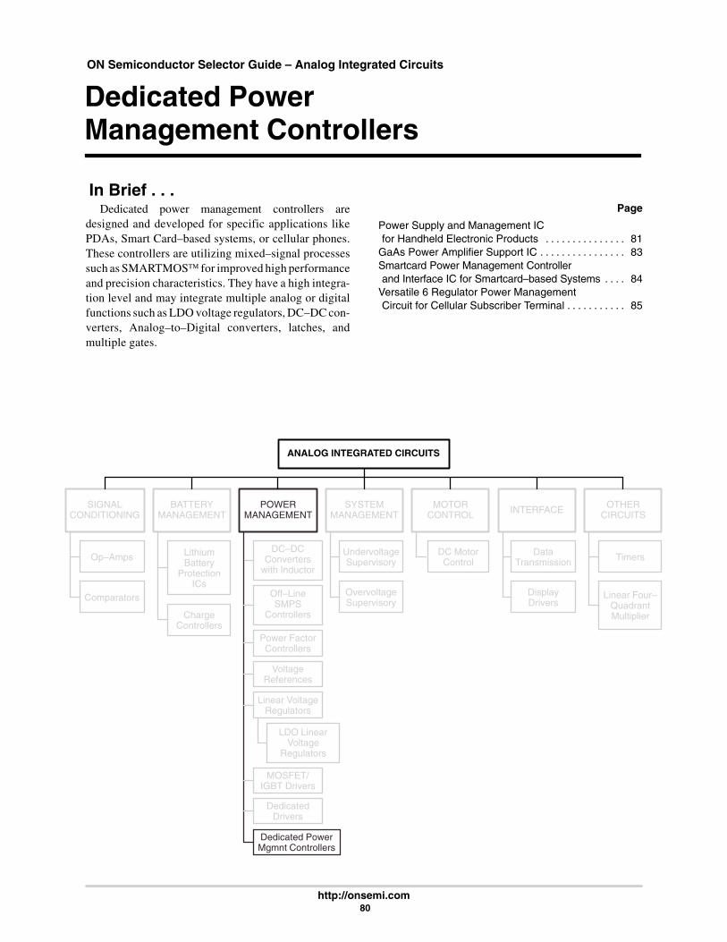
ANALOG INTEGRATED CIRCUITS
SIGNALCONDITIONING
BATTERYMANAGEMENT
POWERMANAGEMENT
SYSTEMMANAGEMENT
MOTORCONTROL INTERFACE OTHER
CIRCUITS
Op–Amps
Comparators
LithiumBattery
ProtectionICs
ChargeControllers
DC–DCConverters
with Inductor
Off–LineSMPS
Controllers
UndervoltageSupervisory
OvervoltageSupervisory
DataTransmission
DisplayDrivers
Timers
Linear Four–QuadrantMultiplier
Power FactorControllers
VoltageReferences
Linear VoltageRegulators
LDO LinearVoltage
Regulators
MOSFET/IGBT Drivers
DedicatedDrivers
Dedicated PowerMgmnt Controllers
DC MotorControl
ON Semiconductor Selector Guide – Analog Integrated Circuits
http://onsemi.com 80
Dedicated PowerManagement Controllers
In Brief . . .Dedicated power management controllers are
designed and developed for specific applications likePDAs, Smart Card–based systems, or cellular phones.These controllers are utilizing mixed–signal processessuch as SMARTMOS for improved high performanceand precision characteristics. They have a high integra-tion level and may integrate multiple analog or digitalfunctions such as LDO voltage regulators, DC–DC con-verters, Analog–to–Digital converters, latches, andmultiple gates.
Page
Power Supply and Management ICfor Handheld Electronic Products 81. . . . . . . . . . . . . . .
GaAs Power Amplifier Support IC 83. . . . . . . . . . . . . . . . Smartcard Power Management Controllerand Interface IC for Smartcard–based Systems 84. . . .
Versatile 6 Regulator Power ManagementCircuit for Cellular Subscriber Terminal 85. . . . . . . . . . .

ON Semiconductor Selector Guide – Analog Integrated Circuits
http://onsemi.com 81
Power Supply and Management IC for HandheldElectronic ProductsMC34280
0°C to +70°C, LQFP 32–Pins
The MC34280 is a power supply integrated circuitwhich provides two boost regulated outputs and somepower management supervisory functions. Bothregulators apply Pulse–Frequency–Modulation (PFM).The main step–up regulator output can be externallyadjusted from 2.7V to 5V. An internal synchronousrectifier is used to ensure high efficiency (achieve 87%).The auxiliary regulator with a built–in power transistorcan be configured to produce a wide range of positivevoltage (can be used for LCD contrast voltage). Thisvoltage can be adjusted from +5V to +25V by an externalpotentiometer; or by a microprocessor, digitally througha 6–bit internal DAC.
The MC34280 has been designed for battery poweredhand–held products. With the low start–up voltage from1V and the low quiescent current (typical 35 µA); theMC34280 is best suited to operate from 1 to 2 AA/ AAAcell. Moreover, supervisory functions such as low batterydetection, CPU power–on reset, and back–up batterycontrol, are also included in the chip. It makes the
MC34280 the best one–chip power management solutionfor applications such as electronic organizers and PDAs.• Low Input Voltage, 1V up• Low Quiescent Current in Standby Mode: 35µA
typical• PFM and Synchronous Rectification to ensure high
efficiency (87% @200mA Load)• Adjustable Main Output: nominal 3.3V @ 200mA
max, with 1.8V input• Auxiliary Output Voltage can be digitally controlled
by microprocessor• Auxiliary Output Voltage:
+5V @ 25mA max, with 1.8V input +25V @ 15mA max, with 1.8V input
• Current Limit Protection• Power–ON Reset Signal with Programmable Delay• Battery Low Detection• Lithium Battery Back–up• 32–Pin LQFP Package
ORDERING INFORMATION
DeviceOperating
Temperature Range Package
MC34280 0°C to +70°C 32–pin LQFP
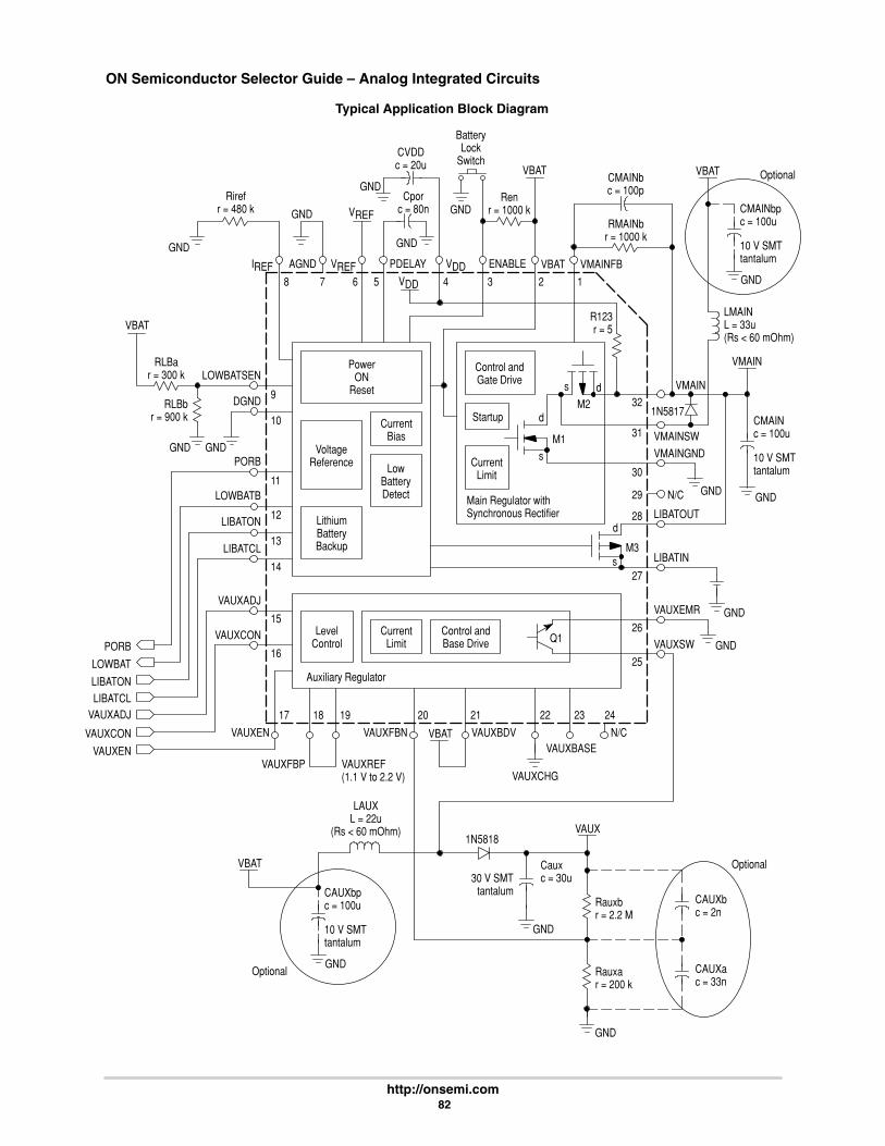
ON Semiconductor Selector Guide – Analog Integrated Circuits
http://onsemi.com 82
PowerON
Reset
LithiumBatteryBackup
VoltageReference Low
BatteryDetect
CurrentBias
Control andGate Drive
Startup
CurrentLimit
Main Regulator withSynchronous Rectifier
LIBATCL
LIBATON
LOWBATB
PORB
DGND
LOWBATSEN
14
13
12
11
10
9
GNDGND
RLBbr = 900 k
RLBar = 300 k
LIBATIN
27
28
29
30
31
32
GNDN/C
LIBATOUT
VMAINGND
VMAINSW
1N5817M2
M1
IREF AGND
8 7
VREF
VBAT
GND
RMAINbr = 1000 k
CMAINbc = 100p
VBAT
VMAIN
PDELAY VDDVDD
VMAINFBVBAT
6 5 4
VREF
GND
GNDRen
r = 1000 k
VBAT
BatteryLock
Switch
VMAIN
GND
CVDDc = 20u
3 2 1
ENABLE
Rirefr = 480 k
R123r = 5
CMAINc = 100u
10 V SMTtantalum
LMAINL = 33u(Rs < 60 mOhm)
GND
Optional
CMAINbpc = 100u
10 V SMTtantalum
M3
d
s
d
s
ds
GND GND
Typical Application Block Diagram
Cporc = 80n
VAUXADJ
15VAUXCON
16
VAUXEN
17
VBAT
LIBATCL
LIBATON
LOWBAT
PORB
VAUXADJ
VAUXCON
VAUXENVAUXFBP
GNDOptional
CAUXbpc = 100u
10 V SMTtantalum
VBAT
18 20 2119 22 23 24
LevelControl
CurrentLimit
Auxiliary Regulator
Control andBase Drive
LAUXL = 22u
(Rs < 60 mOhm)
VAUXFBN
GND
Cauxc = 30u30 V SMT
tantalum
VAUX1N5818
GND
GND
VAUXREF(1.1 V to 2.2 V)
VAUXBDV
VAUXCHG
VAUXBASEN/C
Rauxbr = 2.2 M
Rauxar = 200 k
GND
CAUXbc = 2n
CAUXac = 33n
Q1
VAUXEMR
26VAUXSW
25
Optional
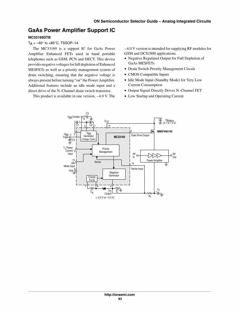
ON Semiconductor Selector Guide – Analog Integrated Circuits
http://onsemi.com 83
GaAs Power Amplifier Support ICMC33169DTB
TA = –40° to +85°C, TSSOP–14
The MC33169 is a support IC for GaAs PowerAmplifier Enhanced FETs used in hand portabletelephones such as GSM, PCN and DECT. This deviceprovides negative voltages for full depletion of EnhancedMESFETs as well as a priority management system ofdrain switching, ensuring that the negative voltage isalways present before turning “on” the Power Amplifier.Additional features include an idle mode input and adirect drive of the N–Channel drain switch transistor.
This product is available in one version, –4.0 V. The
–4.0 V version is intended for supplying RF modules forGSM and DCS1800 applications.• Negative Regulated Output for Full Depletion of
GaAs MESFETs
• Drain Switch Priority Management Circuit
• CMOS Compatible Inputs
• Idle Mode Input (Standby Mode) for Very LowCurrent Consumption
• Output Signal Directly Drives N–Channel FET
• Low Startup and Operating Current
VBB DoubleC3
VCC+ –
C1
– +
C2
VBBTriple
C4+–
Tx PowerControl
Input
IdleMode Input
Gnd
Cp
+–VO
Output(– 2.5 V or – 4.0 V)
Ci
Rf
Cf+–
+
RFIn
RFOut
+VBattery
(2.7 to 7.0 V)
Gate Drive Output
Sense Input
VBBGenerator
(Voltage Tripler)
PriorityManagement
NegativeGeneratorCharge
Pump
Power AmplifierSense
MC33169
MMSF4N01HD
2 1 14
8
10
457
6
13
9
311
+12
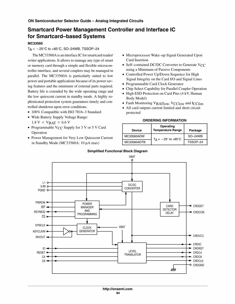
ON Semiconductor Selector Guide – Analog Integrated Circuits
http://onsemi.com 84
Smartcard Power Management Controller and Interface ICfor Smartcard–based SystemsMC33560
TA = 25°C to +85°C, SO–24WB, TSSOP–24
The MC33560A is an interface IC for smartcard reader/writer applications. It allows to manage any type of smartor memory card through a simple and flexible microcon-troller interface, and several couplers may be managed inparallel. The MC33560A is particularly suited to lowpower and portable applications because of its power sav-ing features and the minimum of external parts required.Battery life is extended by the wide operating range andthe low quiescent current in standby mode. A highly so-phisticated protection system guarantees timely and con-trolled shutdown upon error conditions.• 100% Compatible with ISO 7816–3 Standard• Wide Battery Supply Voltage Range:
1.8 V VBAT 6.6 V• Programmable VCC Supply for 3 V or 5 V Card
Operation• Power Management for Very Low Quiescent Current
in Standby Mode (MC33560A: 10 µA max)
• Microprocessor Wake–up Signal Generated UponCard Insertion
• Self–contained DC/DC Converter to Generate VCCusing a Minimum of Passive Components
• Controlled Power Up/Down Sequence for HighSignal Integrity on the Card I/O and Signal Lines
• Programmable Card Clock Generator• Chip Select Capability for Parallel Coupler Operation• High ESD Protection on Card Pins (4 kV, Human
Body Model)• Fault Monitoring VBATlow, VCClow and ICClim• All card outputs current limited and short circuit
protected
ORDERING INFORMATION
DeviceOperating
Temperature Range Package
MC33560ADWTA =25° to +85°C
SO–24WB
MC33560ADTBTA = 25° to +85°C
TSSOP–24
DC/DCCONVERTER
CARDDETECTOR
DELAY
POWERMANAGER
ANDPROGRAMMING
CRDIOCRDRSTCRDC4CRDC8CRDCLKCRDGND
LEVELTRANSLATOR
IO
C4C8
RESET
VBAT
CRDVCC
CRDDET
CRDCON
CLOCKGENERATOR
INVOUT
ASYCLKIN
SYNCLK
CS
RDYMOD
INT
PWRON
PGNDILIM
L1
VBAT
Simplified Functional Block Diagram
ON Semiconductor Selector Guide – Analog Integrated Circuits
http://onsemi.com 85
Versatile 6 Regulator Power Management Circuit for CellularSubscriber TerminalMC33283
TA = 20°C to +70°C, TQFP–32
The MC33283 is a complete power managementsolution for portable devices such as telephone handsets,two–way radios, etc. Thanks to its large scale integration,the device offers up to seven Low DropOut regulators(LDO), two of them delivering a voltage higher than thebattery’s.
Despite the presence of an internal charge pump, theoverall noise specification makes the circuit an idealcandidate where noise is an important feature. Outputsdeliver 40µVRMS typical (10–100kHz) at nominaloutput current.
With a 50dB ripple rejection under 10kHz, the circuitnaturally shields the downstream electronics against DCchoppy lines. This parameter guarantees a clean opera-tion for battery operated devices.
Finally, housed in a compact Thin Quad Flat PackTQFP–32 package, the MC33283 gathers all the featuresnecessary to power future portable radios.• 6 regulated outputs:
2.85V, four outputs: 10–135mA4.75V @ 15mA5.0V @ 20mA
• Low–noise: 40µVRMS at nominal output levels(10Hz–100kHz)
• Ultra–low reverse current in OFF mode (200nAtypical)
• Two–mode regulator: output 5 switches from 3 to5V with SEL pin activated
• Thermal shutdown for a rugged and reliableoperation
• All outputs are short–circuit proof
ORDERING INFORMATION
DeviceOperating
Temperature Range Package
MC33283FTB28,R2 20°C to +70°C TQFP–32

ON Semiconductor Selector Guide – Analog Integrated Circuits
http://onsemi.com 86
Simplified Block Diagram
BUB
OUT1
OUT2
OUT3
OUT5
OUT6
OUT7
GNDVinGND CPB1D1
CHARGE PUMP
ON/OFF6Vref
ON/OFF7Vref
R6
R7
VCC1
VCC1
UVLO1
Vref
ON/OFF2Vref
ON/OFF3Vref
R5A
R5B
ON/OFF5
Vref
Vref
POR
UVLO2
CBYP
ENRS
EN2
EN3
EN5
EN6
EN7
SEL
ON/OFF2ON/OFF3ON/OFF4ON/OFF5ON/OFF6
R2
R3
R1
REFERENCEVOLTAGE
HIGH = UVLOACTIVE
OVLO
13 15 7 14 1
VS 1 IN14
18
30
19
20
21
28
27
26
22
10
2
4
6
31
3
1223
ENABLESWITCHES
VCC1VCC2
529
700 k
VR1
VR1
VCC2
5 A
UVLO1UVLO2
Vref
OUT5 VOLTAGESELECTION
VCC2
OVLO CP ENABLE VCC2
6.5 V
VCC_CP
VCC2
VR1
2 AVCC1
VCC1
VCC1
VCC2
VCC1
ANALOG INTEGRATED CIRCUITS
SIGNALCONDITIONING
BATTERYMANAGEMENT
POWERMANAGEMENT
SYSTEMMANAGEMENT
MOTORCONTROL INTERFACE OTHER
CIRCUITS
Op–Amps
Comparators
LithiumBattery
ProtectionICs
ChargeControllers
DC–DCConverters
with Inductor
Off–LineSMPS
Controllers
UndervoltageSupervisory
OvervoltageSupervisory
DataTransmission
DisplayDrivers
Timers
Linear Four–QuadrantMultiplier
Power FactorControllers
VoltageReferences
Linear VoltageRegulators
LDO LinearVoltage
Regulators
MOSFET/IGBT Drivers
DedicatedDrivers
Dedicated PowerMgmnt Controllers
DC MotorControl
ON Semiconductor Selector Guide – Analog Integrated Circuits
http://onsemi.com 87
System Management
In Brief . . .Power supplies, MCU–based systems, industrial con-
trols, computer systems and many other products, portableor not, are requiring system management functions whichmonitor voltages to ensure proper system operation.
These circuits monitor critical circuit conditions andreport any violations of prescribed limits to a microproces-sor. The microprocessor will then take appropriate actionsuch as storing data before executing a graceful shutdown.
ON Semiconductor offers a wide variety of voltagesupervisory circuits (Undervoltage or Overvoltage)designed for use where precise voltage limits or win-dows are required for reliable system operation.
Newer supervisory circuits have utilized CMOStechnology and miniature surface mount packages(SOT23–5 leads) to reduce the current consumption andthe PCB board area. This makes them particularly suitedfor battery–powered applications.
PageSupervisory Circuits 88. . . . . . . . . . . . . . . . . . . . . . . . . . .
Overvoltage Crowbar Sensing Circuit 88. . . . . . . . . . Over/Undervoltage Protection Circuit 89. . . . . . . . . . Micropower Undervoltage Sensing Circuits 90. . . . . Micropower Undervoltage Sensing Circuitswith Programmable Output Delay 91. . . . . . . . . . . . .
Undervoltage Sensing Circuit 92. . . . . . . . . . . . . . . . . Universal Voltage Monitor 93. . . . . . . . . . . . . . . . . . . .

ON Semiconductor Selector Guide – Analog Integrated Circuits
http://onsemi.com 88
Supervisory CircuitsA variety of Power Supervisory Circuits are offered.
Overvoltage sensing circuits which drive ‘‘Crowbar’’SCRs are provided in several configurations from a lowcost three–terminal version to 8–pin devices which
provide pin–programmable trip voltages or additionalfeatures, such as an indicator output drive and remoteactivation capability. An over/undervoltage protectioncircuit is also offered.
Overvoltage Crowbar Sensing CircuitMC3423P1, D
TA = 0° to +70°C, DIP–8, SO–8 Packages
This device can protect sensitive circuitry frompower supply transients or regulator failure when usedwith an external ‘‘Crowbar’’ SCR. The device sensesvoltage and compares it to an internal 2.6 V reference.Overvoltage trip is adjustable by means of an external
resistive voltage divider. A minimum duration beforetrip is programmable with an external capacitor. Otherfeatures include a 300 mA high current output for driv-ing the gate of a ‘‘Crowbar’’ SCR, an open–collectorindicator output and remote activation capability.
VCC
Sense 1
CurrentSource
Output
VEE Sense 2Remote
Activation
IndicatorOutput
Vref2.6 V
200 µA
2
1
4
8
6537

ON Semiconductor Selector Guide – Analog Integrated Circuits
http://onsemi.com 89
Over/Undervoltage Protection CircuitMC3425P1
TA = 0° to +70°C, DIP–8 Package
The MC3425 is a power supply supervisory circuitcontaining all the necessary functions required tomonitor over and undervoltage fault conditions. Thisdevice features dedicated over and undervoltagesensing channels with independently programmabletime delays. The overvoltage channel has a high current
drive output for use in conjunction with an external SCR‘‘Crowbar’’ for shutdown. The undervoltage channelinput comparator has hysteresis which is externallyprogrammable, and an open–collector output for faultindication.
OVSense
UVSense
VCC
OVDrive
UVIndicator
Input Section Output SectionUVDLY
OVDLY
Gnd
200 µA
200 µA
12.5 µA
IH 2.5 VVref
8
1
6
3
4
5 2 7
ON Semiconductor Selector Guide – Analog Integrated Circuits
http://onsemi.com 90
Supervisory Circuits (continued)
Micropower Undervoltage Sensing CircuitsMC33464H, NTA = –30° to +80°C, SOT–89, SOT–23 5 Leads Packages
The MC33464 series are micropower undervoltagesensing circuits that are specifically designed for usewith battery powered microprocessor based systems,where extended battery life is required. A choice of sev-eral threshold voltages from 0.9 V to 4.5 V are available.These devices feature a very low quiescent bias currentof 0.8 µA typical.
The MC33464 series features a highly accuratevoltage reference, a comparator with precise thresholdsand built–in hysteresis to prevent erratic reset operation,a choice of output configurations between open drain orcomplementary MOS, and guaranteed operation below1.0 V with extremely low standby current. Thesedevices are available in either SOT–89 3–pin or
SOT–23 5–pin surface mount packages.Applications include direct monitoring of the
MPU/logic power supply used in portable, appliance,automotive and industrial equipment.MC33464 Features:• Extremely Low Standby Current of 0.8 µA at Vin =
1.5 V• Wide Input Voltage Range (0.7 V to 10 V)• Monitors Power Supply Voltages from 1.1 V to 5.0 V• High Accuracy Detector Threshold (±2.5%)• Two Reset Output Types (Open Drain or
Complementary Drive)• Two Surface Mount Packages (SOT–89 or SOT–23
5–Pin)
ORDERING INFORMATION
DeviceThreshold
Voltage TypeOperating
Temperature RangePackage
(Qty/Reel)
MC33464H–09AT1 0.9MC33464H–20AT1 2.0 OpenMC33464H–27AT1 2.7 DrainMC33464H–30AT1 3.0 ResetMC33464H–45AT1 4.5 SOT–89
MC33464H–09CT1 0.9 (1000)
MC33464H–20CT1 2.0 Compl.
MC33464H–27CT1 2.7 MOSMC33464H–30CT1 3.0 ResetMC33464H–45CT1 4.5
MC33464N–09ATR 0.9 TA = –30° to +80°CMC33464N–20ATRMC33464N–21ATR
2.02.1
Open
DrainMC33464N–27ATR 2.7
Drain
ResetMC33464N–30ATR 3.0 ResetSOT–23
MC33464N–45ATR 4.5 (3000)
MC33464N–09CTR 0.9
( )5 Leads
MC33464N–20CTR 2.0 Compl.
MC33464N–27CTR 2.7 MOSMC33464N–30CTR 3.0 ResetMC33464N–45CTR 4.5
Other voltages from 0.9 to 6.0 V, in 0.1 V increments, are available. Consult factory for information.
MC33464X–YYATZ Open Drain Configuration MC33464X–YYCTZ Complementary Drive Configuration
X Denotes Package TypeYY Denotes Threshold VoltageTZ Denotes Taping Type
Vref
2 Input
1
Reset
3 Gnd
Vref
2 Input
1
Reset
3 Gnd

ON Semiconductor Selector Guide – Analog Integrated Circuits
http://onsemi.com 91
Supervisory Circuits (continued)
Micropower Undervoltage Sensing Circuits withProgrammable Output DelayMC33465NTA = –30° to +80°C, SOT–23 5 Leads
The MC33465 series are micropower undervoltagesensing circuits that are specifically designed for usewith battery powered microprocessor based systems,where extended battery life is required. A choice ofseveral threshold voltages from 0.9 V to 4.5 V areavailable. This device features a very low quiescent biascurrent of 1.0 µA typical.
The MC33465 series features a highly accuratevoltage reference, a comparator with precise thresholdsand built–in hysteresis to prevent erratic reset operation,a choice of output configurations between open drain orcomplementary, a time delayed output, which can beprogrammed by the system designer, and guaranteedoperation below 1.0 V with extremely low standbycurrent. This device is available in a SOT–23 5–pinsurface mount package.
Applications include direct monitoring of theMPU/logic power supply used in appliance, automotive,industrial and portable equipment.MC33465 Features:• Extremely Low Standby Current of 1.0 µA at Vin =
3.5 V• Wide Input Voltage Range (0.7 V to 10 V)• Monitors Power Supply Voltages from 1.1 V to 5.0 V• High Accuracy Detector Threshold (±2.5%)• Two Reset Output Types (Open Drain or
Complementary Drive)• Programmable Output Delay by External Capacitor
(100 ms typ. with 0.15 µF)• Surface Mount Package (SOT–23 5–Pin)• Convenient Tape and Reel (3000 per Reel)
ORDERING INFORMATION
DeviceThreshold
Voltage TypeOperating
Temperature Range Package
MC33465N–09ATR 0.9MC33465N–20ATR 2.0 OpenMC33465N–27ATR 2.7
O en
DrainMC33465N–30ATRMC33465N–32ATR
3.03.2
Drain
Reset
MC33465N–45ATR 4.5TA 30° to +80°C SOT–23
MC33465N–09CTR 0.9TA = –30° to +80°C
5 Leads
MC33465N–20CTR 2.0 Compl.MC33465N–27CTR 2.7
Com l.
MOSMC33465N–30CTRMC33465N–43CTR
3.04.3
MOS
Reset
MC33465N–45CTR 4.5
Other voltages from 0.9 to 6.0 V, in 0.1 V increments, are available. Consult factory for information.
MC33465N–YYATROpen Drain Output Configuration
MC33465N–YYCTRComplementary Output Configuration
YY Denotes Threshold Voltage
Vref
2 Input
1
Reset
3 Gnd 5 CD
RD
Vref
2 Input
3 Gnd 5 CD
RD
1 Reset
ON Semiconductor Selector Guide – Analog Integrated Circuits
http://onsemi.com 92
Supervisory Circuits (continued)
Undervoltage Sensing CircuitMC34064P–5, D–5, DM–5TA = 0° to +70°C, TO–92, SO–8
MC33064P–5, D–5, DM–5TA = –40° to +85°C, TO–92, SO–8
MC34164P–3, P–5, D–3, D–5, DM–3, DM–5TA = 0° to +70°C, TO–92, SO–8
MC33164P–3, P–5, D–3, D–5, DM–3, DM–5TA = –40° to +85°C, TO–92, SO–8
The MC34064 and MC34164 are two families ofundervoltage sensing circuits specifically designed foruse as reset controllers in microprocessor–based sys-tems. They offer the designer an economical solution forlow voltage detection with a single external resistor.Both parts feature a trimmed bandgap reference, and acomparator with precise thresholds and built–in hyster-esis to prevent erratic reset operation.
The two families of undervoltage sensing circuitstaken together, cover the needs of the most commonlyspecified power supplies used in MCU/MPU systems.Key parameter specifications of the MC34164 familywere chosen to complement the MC34064 series. Thetable summarizes critical parameters of both families.The MC34064 fulfills the needs of a 5.0 V ± 5% systemand features a tighter hysteresis specification. The
MC34164 series covers 5.0 V ± 10% and 3.0 V ± 5%power supplies with significantly lower power con-sumption, making them ideal for applications whereextended battery life is required such as consumer prod-ucts or hand held equipment.
Applications include direct monitoring of the 5.0 VMPU/ logic power supply used in appliance, automo-tive, consumer, and industrial equipment.
The MC34164 is specifically designed for batterypowered applications where low bias current (1/25th ofthe MC34064’s) is an important characteristic.
1 (1)
Input
2 (2)
Gnd3 (4)
Reset
1.2 Vref
Pin numbers inparenthesisare for theD suffix package.
Table 1. Undervoltage Sense/Reset Controller FeaturesMC34X64 devices are specified to operate from 0° to +70°C, and MC33X64 devices operate from –40° to +85°C.
StandardPower
TypicalThreshold
TypicalHysteresis
MinimumOutput
Sink
PowerSupplyInp t
MaximumQ iescent
Device
PowerSupply
Supported
ThresholdVoltage
(V)
HysteresisVoltage
(V)
SinkCurrent
(mA)
InputVoltage
Range (V)
QuiescentInput
Current Package
MC34064/MC33064 5.0 V ± 5% 4.6 0.02 10 1.0 to 10 500 µA@
TO–92@
Vin = 5.0 V SO–8
MC34164/MC33164 5.0 V ± 10% 4.3 0.09 7.0 1.0 to 12 20 µA@
TO–92@
Vin = 5.0 V SO–8
MC34164/MC33164 3.0 V ± 5% 2.7 0.06 6.0 1.0 to 12 15 µA@
TO–92@
Vin = 3.0 V SO–8
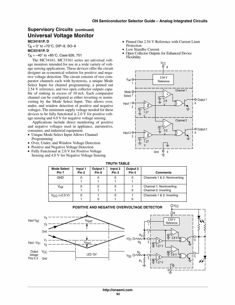
ON Semiconductor Selector Guide – Analog Integrated Circuits
http://onsemi.com 93
Supervisory Circuits (continued)
Universal Voltage MonitorMC34161P, DTA = 0° to +70°C, DIP–8, SO–8MC33161P, DTA = –40° to +85°C, Case 626, 751
The MC34161, MC33161 series are universal volt-age monitors intended for use in a wide variety of volt-age sensing applications. These devices offer the circuitdesigner an economical solution for positive and nega-tive voltage detection. The circuit consists of two com-parator channels each with hysteresis, a unique ModeSelect Input for channel programming, a pinned out2.54 V reference, and two open collector outputs capa-ble of sinking in excess of 10 mA. Each comparatorchannel can be configured as either inverting or nonin-verting by the Mode Select Input. This allows over,under, and window detection of positive and negativevoltages. The minimum supply voltage needed for thesedevices to be fully functional is 2.0 V for positive volt-age sensing and 4.0 V for negative voltage sensing.
Applications include direct monitoring of positiveand negative voltages used in appliance, automotive,consumer, and industrial equipment.• Unique Mode Select Input Allows Channel
Programming• Over, Under, and Window Voltage Detection• Positive and Negative Voltage Detection• Fully Functional at 2.0 V for Positive Voltage
Sensing and 4.0 V for Negative Voltage Sensing
• Pinned Out 2.54 V Reference with Current LimitProtection
• Low Standby Current• Open Collector Outputs for Enhanced Device
Flexibility
2.54 VReference
Channel 1
Channel 2
2.8V
1.27V
0.6V
1.27V
Vref
Gnd
VCC
ModeSelect
Input 1
Input 2
Output 1
Output 2
1
2
3
4
5
6
7
8
TRUTH TABLEMode Select
Pin 7Input 1Pin 2
Output 1Pin 6
Input 2Pin 3
Output 2Pin 5 Comments
GND 01
01
01
01
Channels 1 & 2: Noninverting
Vref 01
01
01
10
Channel 1: NoninvertingChannel 2: Inverting
VCC (>2.0 V) 01
10
01
10
Channels 1 & 2: Inverting
POSITIVE AND NEGATIVE OVERVOLTAGE DETECTOR
+1.27 V
+1.27 V
+2.8 V
+0.6 V
+–
2.54 VReference
–+
–+
+–
4
1
7
2
35
6
R4
R3–VS1
VS2R1
R2
8
VCC
OutputVoltage
Pins 5, 6
Gnd
LED “On”
VHys2
VHys1
VCC
Gnd
Input –VS1
V4
V3
V1V2
Input VS2

ANALOG INTEGRATED CIRCUITS
SIGNALCONDITIONING
BATTERYMANAGEMENT
POWERMANAGEMENT
SYSTEMMANAGEMENT
MOTORCONTROL INTERFACE OTHER
CIRCUITS
Op–Amps
Comparators
LithiumBattery
ProtectionICs
ChargeControllers
DC–DCConverters
with Inductor
Off–LineSMPS
Controllers
UndervoltageSupervisory
OvervoltageSupervisory
DataTransmission
DisplayDrivers
Timers
Linear Four–QuadrantMultiplier
Power FactorControllers
VoltageReferences
Linear VoltageRegulators
LDO LinearVoltage
Regulators
MOSFET/IGBT Drivers
DedicatedDrivers
Dedicated PowerMgmnt Controllers
DC MotorControl
ON Semiconductor Selector Guide – Analog Integrated Circuits
http://onsemi.com 94
Motor Control
In Brief . . .With the expansion of electronics into more and more
mechanical systems, there comes an increasing demand forsimple but intelligent circuits that can blend these two tech-nologies. In the past, the task of power/motor control wasonce accomplished with discrete devices. But today thistask is being performed by bipolar IC technology due tocost, size, and reliability constraints. ON Semiconductoroffers integrated circuits designed to anticipate the require-ments for both simple and sophisticated control systems,while providing cost effective solutions to meet the needs ofthe applications.
PageMotor Controllers 95. . . . . . . . . . . . . . . . . . . . . . . . . . . . . .
Brushless DC Motor Controllers 95. . . . . . . . . . . . . . Closed Loop Brushless Motor Adapter 98. . . . . . . . . DC Servo Motor Controller/Driver 99. . . . . . . . . . . . . Stepper Motor Driver 100. . . . . . . . . . . . . . . . . . . . . . .
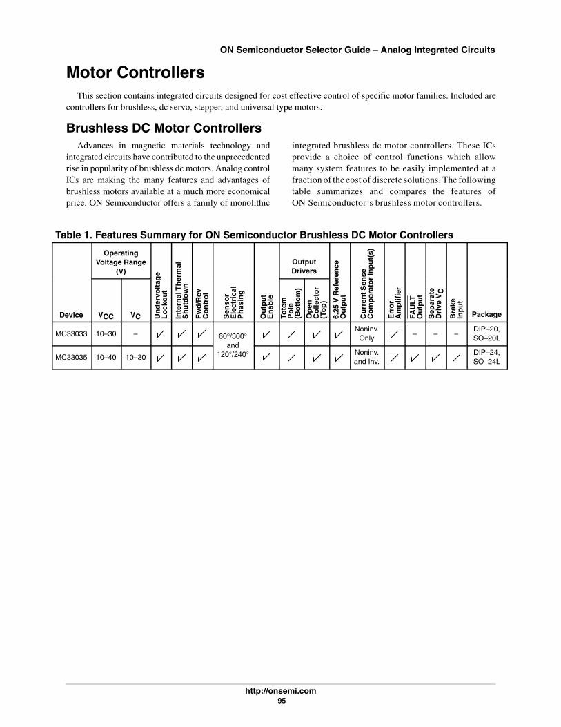
ON Semiconductor Selector Guide – Analog Integrated Circuits
http://onsemi.com 95
Motor ControllersThis section contains integrated circuits designed for cost effective control of specific motor families. Included are
controllers for brushless, dc servo, stepper, and universal type motors.
Brushless DC Motor ControllersAdvances in magnetic materials technology and
integrated circuits have contributed to the unprecedentedrise in popularity of brushless dc motors. Analog controlICs are making the many features and advantages ofbrushless motors available at a much more economicalprice. ON Semiconductor offers a family of monolithic
integrated brushless dc motor controllers. These ICsprovide a choice of control functions which allowmany system features to be easily implemented at afraction of the cost of discrete solutions. The followingtable summarizes and compares the features ofON Semiconductor’s brushless motor controllers.
Table 1. Features Summary for ON Semiconductor Brushless DC Motor Controllers
OperatingVoltage Range
(V)
ge
erm
al
v
OutputDrivers
ren
ce
nse r In
pu
t(s)
Device VCC VC Un
der
volt
agL
ock
ou
t
Inte
rnal
Th
eS
hu
tdo
wn
Fw
d/R
evC
on
tro
l
Sen
sor
Ele
ctri
cal
Ph
asin
g
Ou
tpu
tE
nab
le
Tote
mP
ole
(Bo
tto
m)
Op
enC
olle
cto
r(T
op
)
6.25
V R
efer
Ou
tpu
t
Cu
rren
t Sen
Co
mp
arat
or
Err
or
Am
plif
ier
FAU
LTO
utp
ut
Sep
arat
eD
rive
VC
Bra
keIn
pu
t
Package
MC33033 10–30 – 60°/300°and
Noninv.Only
– – –DIP–20,SO–20L
MC33035 10–40 10–30
and120°/240° Noninv.
and Inv.DIP–24,SO–24L
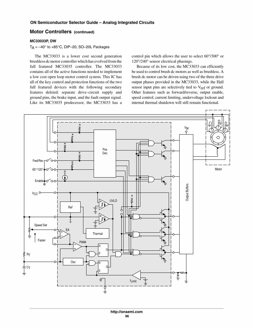
ON Semiconductor Selector Guide – Analog Integrated Circuits
http://onsemi.com 96
Motor Controllers (continued)
MC33033P, DW
TA = –40° to +85°C, DIP–20, SO–20L Packages
The MC33033 is a lower cost second generationbrushless dc motor controller which has evolved from thefull featured MC33035 controller. The MC33033contains all of the active functions needed to implementa low cost open loop motor control system. This IC hasall of the key control and protection functions of the twofull featured devices with the following secondaryfeatures deleted: separate drive–circuit supply andground pins, the brake input, and the fault output signal.Like its MC33035 predecessor, the MC33033 has a
control pin which allows the user to select 60°/300° or120°/240° sensor electrical phasings.
Because of its low cost, the MC33033 can efficientlybe used to control brush dc motors as well as brushless. Abrush dc motor can be driven using two of the three driveoutput phases provided in the MC33033, while the Hallsensor input pins are selectively tied to Vref or ground.Other features such as forward/reverse, output enable,speed control, current limiting, undervoltage lockout andinternal thermal shutdown will still remain functional.
CT
RT
Faster
Speed Set
VCC
Fwd/Rev
60°/120°
Enable
ILimit
VM
Motor
S S
PWM
EA
Osc
Ref
PosDec
UVLO
Thermal
R
SQ
R
SQ
Out
put B
uffe
rs
N
N

ON Semiconductor Selector Guide – Analog Integrated Circuits
http://onsemi.com 97
Motor Controllers (continued)
MC33035P, DW
TA = –40° to +85°C, DIP–24, SO–24L Packages
The MC33035 is a second generation highperformance brushless dc motor controller whichcontains all of the active functions required to implementa full featured open loop motor control system. Whilebeing pin–compatible with an earlier device, theMC33035 offers additional features at a lower price. Thetwo additional features provided by the MC33035 are apin which allows the user to select 60°/300° or 120°/240°
sensor electrical phasings, and access to both invertingand noninverting inputs of the current sense comparator.The earlier devices had two part numbers which wereneeded to support the different sensor phasings, and theinverting input to the current sense comparator wasinternally grounded. All of the control and protectionfeatures of the earlier device are also provided in theMC33035.
PosDec
UVLO
PWM
EA
Osc
Ref
Motor
Thermal
R
R
SQ
SQ
ILimit
Fwd/Rev
60°/120°
Enable
VINVCC
VC
Speed Set
Faster
CT
RT
Brake
FaultVM
S S
Out
put B
uffe
rs
N
N

ON Semiconductor Selector Guide – Analog Integrated Circuits
http://onsemi.com 98
Motor Controllers (continued)
Closed Loop Brushless Motor AdapterMC33039P, D
TA = –40° to +85°C, DIP–8, SO–8
The MC33039 is a high performance close loop speedcontrol adapter specifically designed for use in brushlessdc motor control systems. Implementation will allowprecise speed regulation without the need for a magneticor optical tachometer. These devices contain three inputbuffers each with hysteresis for noise immunity, threedigital edge detectors, a programmable monostable, and
an internal shunt regulator. Also included is an inverteroutput for use in systems that require conversion ofsensor phasing. Although this device is primarilyintended for use with the MC33033/35 brushless motorcontrollers, it can be used cost effectively in many otherclosed loop speed control applications.
Delay
Delay
Delay
VCC
Φ C
Φ A
Φ B
Φ A
Q
To RotorPositionSensors
20 k
8.25 V
S
R
0.3 V
Gnd
15 k
R
R2
RT
CT
fout
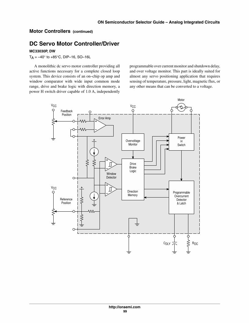
ON Semiconductor Selector Guide – Analog Integrated Circuits
http://onsemi.com 99
Motor Controllers (continued)
DC Servo Motor Controller/DriverMC33030P, DW
TA = –40° to +85°C, DIP–16, SO–16L
A monolithic dc servo motor controller providing allactive functions necessary for a complete closed loopsystem. This device consists of an on–chip op amp andwindow comparator with wide input common moderange, drive and brake logic with direction memory, apower H switch driver capable of 1.0 A, independently
programmable over current monitor and shutdown delay,and over voltage monitor. This part is ideally suited foralmost any servo positioning application that requiressensing of temperature, pressure, light, magnetic flux, orany other means that can be converted to a voltage.
VCC
FeedbackPosition
ReferencePosition
WindowDetector
Error Amp
OvervoltageMonitor
DriveBrakeLogic
DirectionMemory
PowerH
Switch
ProgrammableOvercurrent
Detector& Latch
Motor
CDLY ROC
VCC
VCC
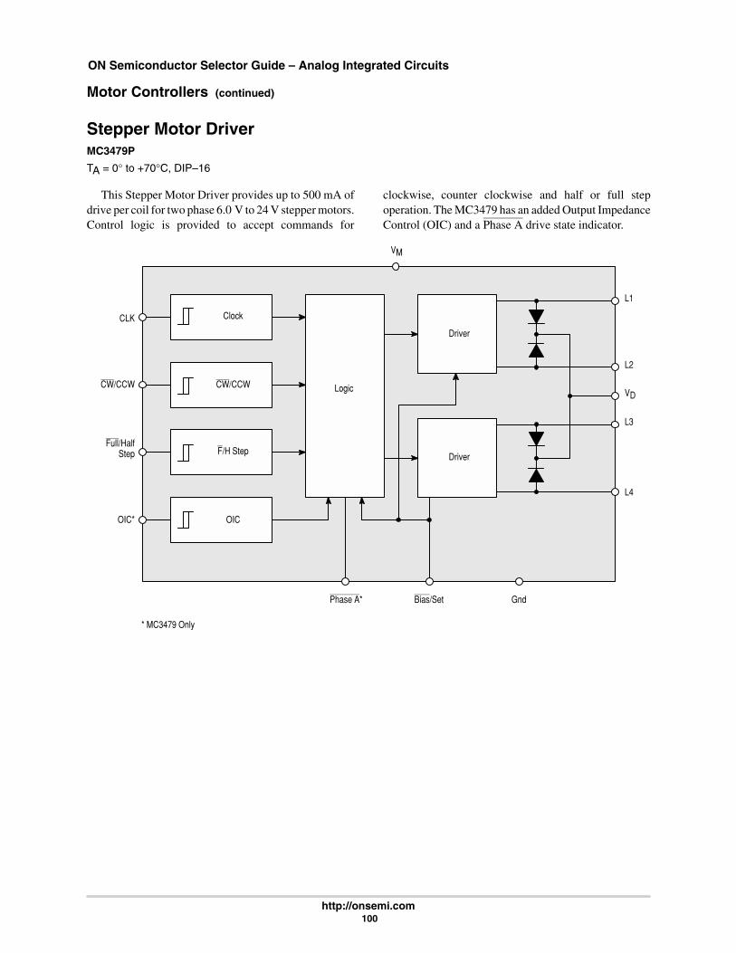
ON Semiconductor Selector Guide – Analog Integrated Circuits
http://onsemi.com 100
Motor Controllers (continued)
Stepper Motor DriverMC3479P
TA = 0° to +70°C, DIP–16
This Stepper Motor Driver provides up to 500 mA ofdrive per coil for two phase 6.0 V to 24 V stepper motors.Control logic is provided to accept commands for
clockwise, counter clockwise and half or full stepoperation. The MC3479 has an added Output ImpedanceControl (OIC) and a Phase A drive state indicator.
Full/HalfStep
Clock
CW/CCW
F/H Step
OIC
CLK
CW/CCW
OIC*
L1
Logic
Driver
Driver
Phase A* Bias/Set Gnd
L2
VD
L3
L4
VM
* MC3479 Only

ANALOG INTEGRATED CIRCUITS
SIGNALCONDITIONING
BATTERYMANAGEMENT
POWERMANAGEMENT
SYSTEMMANAGEMENT
MOTORCONTROL INTERFACE OTHER
CIRCUITS
Op–Amps
Comparators
LithiumBattery
ProtectionICs
ChargeControllers
DC–DCConverters
with Inductor
Off–LineSMPS
Controllers
UndervoltageSupervisory
OvervoltageSupervisory
DataTransmission
DisplayDrivers
Timers
Linear Four–QuadrantMultiplier
Power FactorControllers
VoltageReferences
Linear VoltageRegulators
LDO LinearVoltage
Regulators
MOSFET/IGBT Drivers
DedicatedDrivers
Dedicated PowerMgmnt Controllers
DC MotorControl
ON Semiconductor Selector Guide – Analog Integrated Circuits
http://onsemi.com 101
Interface
In Brief . . .Described in this section is ON Semiconductor’s line
of interface circuits, which provide the means for inter-facing with microprocessor or digital systems and theexternal world, or to other systems.
Also included are devices which allow a micropro-cessor to communicate with its own array of memory andperipheral I/O circuits.
The line drivers, receivers, and transceivers permitcommunication between systems over cables of severalthousand feet in length, and at data rates of up to severalmegahertz. The common EIA data transmission stan-dards, several European standards, and IEEE–488 areaddressed by these devices.
PageLine Receivers 102. . . . . . . . . . . . . . . . . . . . . . . . . . . . . . .
EIA Standard 102. . . . . . . . . . . . . . . . . . . . . . . . . . . . . . Line Drivers 102. . . . . . . . . . . . . . . . . . . . . . . . . . . . . . . . .
EIA Standard 102. . . . . . . . . . . . . . . . . . . . . . . . . . . . . . Peripheral Drivers 102. . . . . . . . . . . . . . . . . . . . . . . . .
Display Drivers 103. . . . . . . . . . . . . . . . . . . . . . . . . . . . . . . Electroluminescent (EL) Lamp Driver 103. . . . . . . . .
The peripheral drivers are designed to handle highcurrent loads such as relay coils, lamps, stepper motors,and others. Input levels to these drivers can be TTL,CMOS, high voltage MOS, or other user defined levels.The display drivers are designed for LCD or LED dis-plays, and provide various forms of decoding.

ON Semiconductor Selector Guide – Analog Integrated Circuits
http://onsemi.com 102
Line ReceiversTable 1. EIA Standard
S = SingleEnded
Typeof
tpropDelayTime
PartyLine Strobe Power S ffix/ Receivers ComEnded
D = Differ-ential
ofOut–put
TimeMax(ns)
LineOpera–
tion
Strobeor
Enable
PowerSupplies
(V) Device
Suffix/Pack–
age
ReceiversPer
Package
Com–panionDrivers Comments
S TP 4000 – – +5.0 MC14C89AB DIP–16,SO–16
4 MC1488MC14C88B
EIA–232–D/EIA–562
R(1) 85 – – MC1489MC1489A
EIA–232–D
(1) R = Resistor Pull–up, TP = Totem–pole output.
Line DriversTable 2. EIA StandardOutputCurrentCapa
tpropDelayTime
S = SingleEnded
PartyLine Strobe Power S ffix/
DriversPerCapa–
bility(mA)
TimeMax(ns)
EndedD = Differ-
ential
LineOpera–
tion
Strobeor
Enable
PowerSupplies
(V) Device
Suffix/Pack–
age
PerPack–
ageCompanionReceivers Comments
85 35 D +5.0 MC75174BMC75172B
SO–20L 4 – EIA–485
15 3500 S – ±7.0 to±12
MC14C88B DIP–8,SO–8
MC14C89BMC14C89AB
EIA–232–D/EIA–562
10 350 ±9.0 to±12
MC1488 MC1489MC1489A
EIA–232–D
60 300 S/D EIA–422EIA–
423 –
±5.0 MC26LS30 SO–16 4 (423)2 (422)
– EIA–422 orEIA–423Switchable
Table 3. Peripheral Drivers OutputCurrent Propagation Output Off State Drivers
Capability(mA)
InputCapability
p gDelay Time
Max (µs)
pClampDiode
VoltageMax (V) Device
PerPackage
Suffix/Package
LogicFunction
500 TTL, CMOS 1.0 50 ULN2803 8 DIP–18 Invert
6.0 V to 15 VMOS
ULN2804
TTL, 5.0 VCMOS
MC1413, B(ULN2003A)
7 DIP–16,SO–16
8.0 V to 18 VMOS
MC1416, B(ULN2004A)
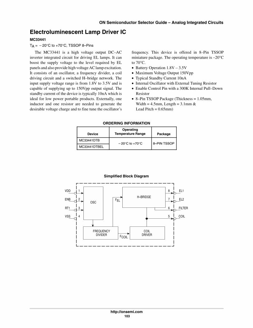
ON Semiconductor Selector Guide – Analog Integrated Circuits
http://onsemi.com 103
Electroluminescent Lamp Driver ICMC33441
TA = 20°C to +70°C, TSSOP 8–Pins
The MC33441 is a high voltage output DC–ACinverter integrated circuit for driving EL lamps. It canboost the supply voltage to the level required by ELpanels and also provide high voltage AC lamp excitation.It consists of an oscillator, a frequency divider, a coildriving circuit and a switched H–bridge network. Theinput supply voltage range is from 1.8V to 3.5V and iscapable of supplying up to 150Vpp output signal. Thestandby current of the device is typically 10nA which isideal for low power portable products. Externally, oneinductor and one resistor are needed to generate thedesirable voltage charge and to fine tune the oscillator’s
frequency. This device is offered in 8–Pin TSSOPminiature package. The operating temperature is –20°Cto 70°C.• Battery Operation 1.8V – 3.5V• Maximum Voltage Output 150Vpp• Typical Standby Current 10nA• Internal Oscillator with External Tuning Resistor• Enable Control Pin with a 300K Internal Pull–Down
Resistor• 8–Pin TSSOP Package (Thickness = 1.05mm,
Width = 4.5mm, Length = 3.1mm &Lead Pitch = 0.65mm)
ORDERING INFORMATION
DeviceOperating
Temperature Range Package
MC33441DTB20°C to +70°C 8–PIN TSSOP
MC33441DTBEL20°C to +70°C 8–PIN TSSOP
Simplified Block Diagram
FREQUENCYDIVIDER
VDD
ENB
RT1
OSCFEL
VSS
1
2
3
4
H–BRIDGE
COILDRIVERFCOIL
EL1
EL2
FILTER
COIL
8
7
6
5
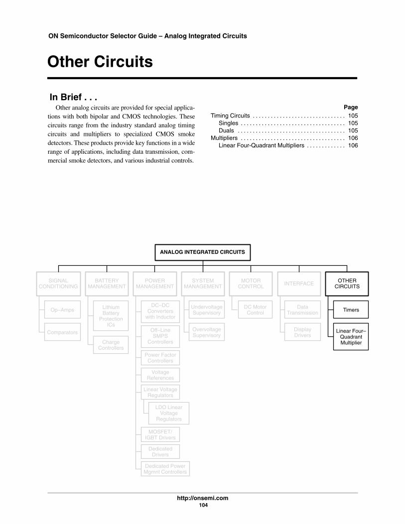
ANALOG INTEGRATED CIRCUITS
SIGNALCONDITIONING
BATTERYMANAGEMENT
POWERMANAGEMENT
SYSTEMMANAGEMENT
MOTORCONTROL INTERFACE OTHER
CIRCUITS
Op–Amps
Comparators
LithiumBattery
ProtectionICs
ChargeControllers
DC–DCConverters
with Inductor
Off–LineSMPS
Controllers
UndervoltageSupervisory
OvervoltageSupervisory
DataTransmission
DisplayDrivers
Timers
Linear Four–QuadrantMultiplier
Power FactorControllers
VoltageReferences
Linear VoltageRegulators
LDO LinearVoltage
Regulators
MOSFET/IGBT Drivers
DedicatedDrivers
Dedicated PowerMgmnt Controllers
DC MotorControl
ON Semiconductor Selector Guide – Analog Integrated Circuits
http://onsemi.com 104
Other Circuits
In Brief . . .Other analog circuits are provided for special applica-
tions with both bipolar and CMOS technologies. Thesecircuits range from the industry standard analog timingcircuits and multipliers to specialized CMOS smokedetectors. These products provide key functions in a widerange of applications, including data transmission, com-mercial smoke detectors, and various industrial controls.
PageTiming Circuits 105. . . . . . . . . . . . . . . . . . . . . . . . . . . . . . .
Singles 105. . . . . . . . . . . . . . . . . . . . . . . . . . . . . . . . . . . Duals 105. . . . . . . . . . . . . . . . . . . . . . . . . . . . . . . . . . . .
Multipliers 106. . . . . . . . . . . . . . . . . . . . . . . . . . . . . . . . . . . Linear Four-Quadrant Multipliers 106. . . . . . . . . . . . .

ON Semiconductor Selector Guide – Analog Integrated Circuits
http://onsemi.com 105
Timing CircuitsThese highly stable timers are capable of producing
accurate time delays or oscillation. In the time delay modeof operation, the time is precisely controlled by oneexternal resistor and capacitor. For a stable operation as anoscillator, the free–running frequency and the duty cycleare both accurately controlled with two external resistorsand one capacitor. The output structure can source or sinkup to 200 mA or drive TTL circuits. Timing intervals frommicroseconds through hours can be obtained. Additionalterminals are provided for triggering or resetting ifdesired.
SinglesMC1455P1, DTA = 0° to +70°C, SO–8, DIP–8
MC1455BP1, D
TA = –40° to +85°C, SO–8, DIP–8
Comp B
Comp A7
VCC
Threshold
ControlVoltage
Trigger
5
6
2
Gnd1
3
Discharge
Output
5.0 k
R
S
FlipFlop
Inhibit/Reset
Q
8
5.0 k
5.0 k
Reset4
Duals
MC3456PTA = 0° to +70°C, DIP–14
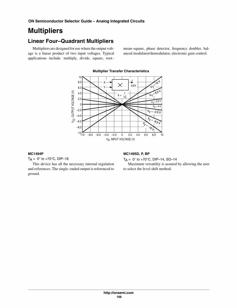
ON Semiconductor Selector Guide – Analog Integrated Circuits
http://onsemi.com 106
MultipliersLinear Four–Quadrant Multipliers
Multipliers are designed for use where the output volt-age is a linear product of two input voltages. Typicalapplications include: multiply, divide, square, root–
mean–square, phase detector, frequency doubler, bal-anced modulator/demodulator, electronic gain control.
k =110
–10VX, INPUT VOLTAGE (V)
–10
–8.0
–4.0
–2.0
0
2.0
–6.0
4.0
6.0
8.0
10, O
UTP
UT
VOLT
AGE
(V)
OV
+X
Y KXY
–8.0 –6.0 –4.0 –2.0 0 2.0 4.0 6.0 8.0 10
Multiplier Transfer Characteristics
MC1494PTA = 0° to +70°C, DIP–16
This device has all the necessary internal regulationand references. The single–ended output is referenced toground.
MC1495D, P, BP
TA = 0° to +70°C, DIP–14, SO–14Maximum versatility is assured by allowing the user
to select the level shift method.

ON Semiconductor Selector Guide – Analog Integrated Circuits
http://onsemi.com 107
Tape and Reel Options
In Brief . . .ON Semiconductor offers the convenience of Tape
and Reel packaging for our growing family of stan-dard integrated circuit products. Reels are available tosupport the requirements of both first and second gen-eration pick–and–place equipment. The packagingfully conforms to the latest EIA–481A specification.The antistatic embossed tape provides a secure cavity,sealed with a peel–back cover tape.
PageTape and Reel Configurations 108. . . . . . . . . . . . . . . . . . Tape and Reel Information Table 110. . . . . . . . . . . . . . . . Analog MPQ Table 111. . . . . . . . . . . . . . . . . . . . . . . . . . .

ON Semiconductor Selector Guide – Analog Integrated Circuits
http://onsemi.com 108
Tape and Reel Configurations
Typical
User Direction of Feed
SOIC and Micro–8DEVICES
PIN 1
Typical
User Direction of Feed
PLCC DEVICES
Typical
User Direction of Feed
DPAK and D2PAKDEVICES
Mechanical Polarization
Typical
User Direction of Feed
SOT–23 (5 Pin)DEVICES
Typical
SOT–89 (3 Pin)DEVICES
User Direction of Feed
Typical
SOT–89 (5 Pin)DEVICES
User Direction of Feed
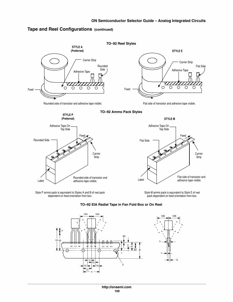
ON Semiconductor Selector Guide – Analog Integrated Circuits
http://onsemi.com 109
Tape and Reel Configurations (continued)
STYLE A(Preferred)
TO–92 Reel Styles
Carrier Strip
Adhesive Tape
RoundedSide
ÉÉÉÉÉÉÉFeed
Rounded side of transistor and adhesive tape visible. Flat side of transistor and adhesive tape visible.
ÉÉÉÉÉÉÉFeed
Adhesive Tape OnTop Side
CarrierStrip
Adhesive Tape OnTop Side
Style M ammo pack is equivalent to Style E of reelpack dependent on feed orientation from box.
ÉÉÉÉÉÉÉÉÉÉÉÉÉÉÉÉÉÉÉÉÉÉÉÉÉÉÉÉÉÉÉÉÉÉÉÉÉÉÉÉ
Flat Side
Label
STYLE MSTYLE P
(Preferred)
ÉÉÉÉÉÉÉÉÉÉÉÉÉÉÉÉÉÉÉÉÉÉÉÉÉÉÉÉÉÉÉÉÉÉÉÉÉÉÉÉ
Rounded Side
Style P ammo pack is equivalent to Styles A and B of reel packdependent on feed orientation from box.
Flat side of transistor andadhesive tape visible.
Rounded side of transistor andadhesive tape visible.
TO–92 Ammo Pack Styles
Carrier Strip
Adhesive TapeFlat Side
Label
CarrierStrip
STYLE E
FeedFeed
H2A H2A
H
F1F2
P2 P2
P1P
D
WW1
L1
W2
H2B H2B
T1
T
T2
H4 H5
H1
L
TO–92 EIA Radial Tape in Fan Fold Box or On Reel
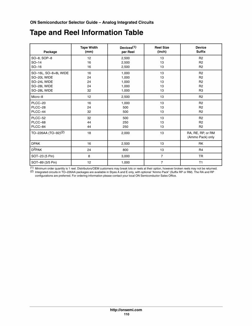
ON Semiconductor Selector Guide – Analog Integrated Circuits
http://onsemi.com 110
Tape and Reel Information Table
Tape Width Devices(1) Reel Size DevicePackage
p(mm)
e cesper Reel (inch) Suffix
SO–8, SOP–8 12 2,500 13 R2SO–14 16 2,500 13 R2SO–16 16 2,500 13 R2
SO–16L, SO–8+8L WIDE 16 1,000 13 R2SO–20L WIDE 24 1,000 13 R2SO–24L WIDE 24 1,000 13 R2SO–28L WIDE 24 1,000 13 R2SO–28L WIDE 32 1,000 13 R3
Micro–8 12 2,500 13 R2
PLCC–20 16 1,000 13 R2PLCC–28 24 500 13 R2PLCC–44 32 500 13 R2
PLCC–52 32 500 13 R2PLCC–68 44 250 13 R2PLCC–84 44 250 13 R2
TO–226AA (TO–92)(2) 18 2,000 13 RA, RE, RP, or RM(Ammo Pack) only
DPAK 16 2,500 13 RK
D2PAK 24 800 13 R4
SOT–23 (5 Pin) 8 3,000 7 TR
SOT–89 (3/5 Pin) 12 1,000 7 T1
(1) Minimum order quantity is 1 reel. Distributors/OEM customers may break lots or reels at their option, however broken reels may not be returned.(2) Integrated circuits in TO–226AA packages are available in Styes A and E only, with optional “Ammo Pack” (Suffix RP or RM). The RA and RP
configurations are preferred. For ordering information please contact your local ON Semiconductor Sales Office.

ON Semiconductor Selector Guide – Analog Integrated Circuits
http://onsemi.com 111
Analog MPQ TableTape/Reel and Ammo Pack
Package Type Package Code MPQPackage Type Package Code MPQ
PLCC
Case 775 0802 1000/reelCase 776 0804 500/reelCase 777 0801 500/reel
SOIC
Case 751 0095 2500/reelCase 751A 0096 2500/reelCase 751B 0097 2500/reelCase 751G 2003 1000/reelCase 751D 2005 1000/reelCase 751E 2008 1000/reelCase 751F 2009 1000/reel
Micro–8
Case 846A – 2500/reel
TO–92
Case 29 0031 2000/reelCase 29 0031 2000/Ammo Pack
DPAK
Case 369A – 2500/reel
D2PAK
Case 936 – 800/reel
SOT–23 (5 Pin)
Case 1212 – 3000/reel
SOT–89 (3 Pin)
Case 1213 – 1000/reel
SOT–89 (5 Pin)
Case 1214 – 1000/reel
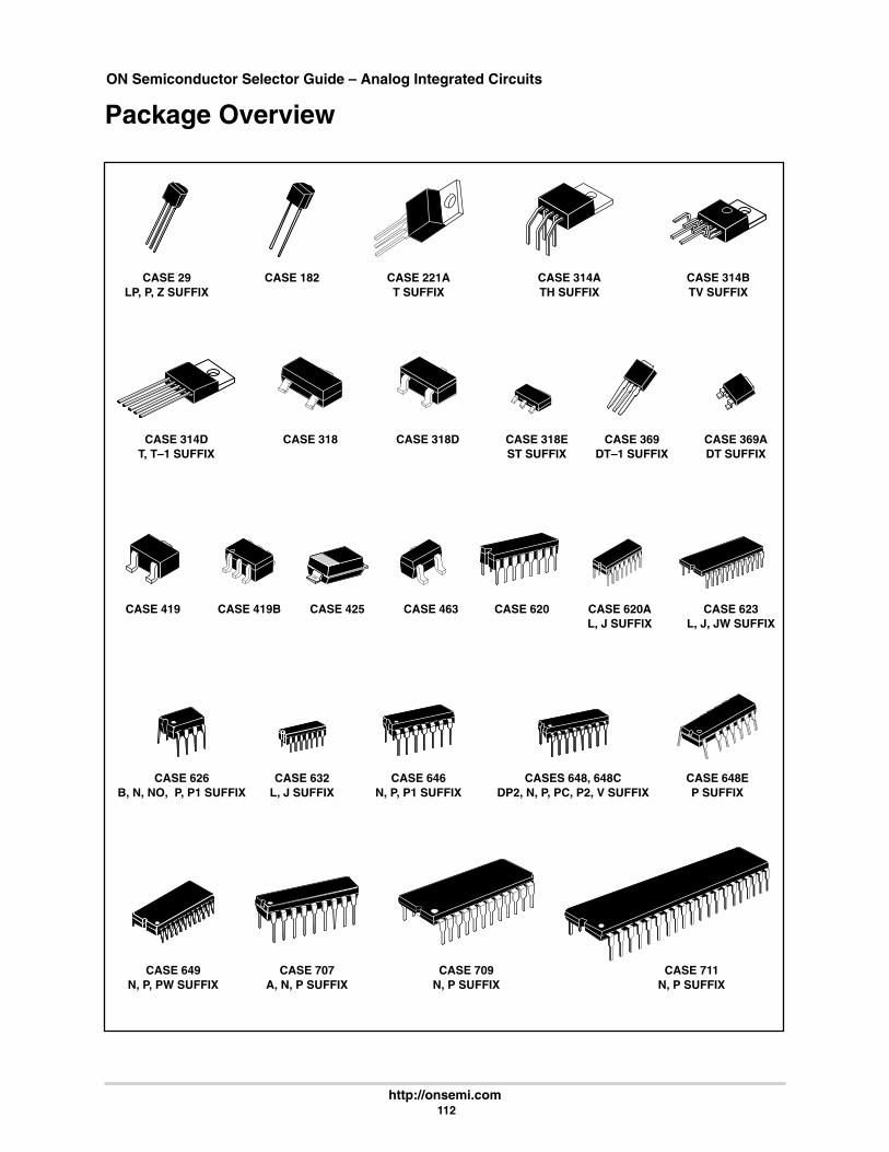
ON Semiconductor Selector Guide – Analog Integrated Circuits
http://onsemi.com 112
Package Overview
CASE 29LP, P, Z SUFFIX
CASE 221AT SUFFIX
CASE 314DT, T–1 SUFFIX
CASE 646N, P, P1 SUFFIX
CASE 369ADT SUFFIX
CASE 648EP SUFFIX
CASE 314BTV SUFFIX
CASE 314ATH SUFFIX
CASE 369DT–1 SUFFIX
CASE 626B, N, NO, P, P1 SUFFIX
CASES 648, 648CDP2, N, P, PC, P2, V SUFFIX
CASE 318EST SUFFIX
CASE 620
CASE 632L, J SUFFIX
CASE 620AL, J SUFFIX
CASE 623L, J, JW SUFFIX
CASE 649N, P, PW SUFFIX
CASE 182
CASE 318 CASE 318D
CASE 425CASE 419 CASE 419B CASE 463
CASE 707A, N, P SUFFIX
CASE 709N, P SUFFIX
CASE 711N, P SUFFIX
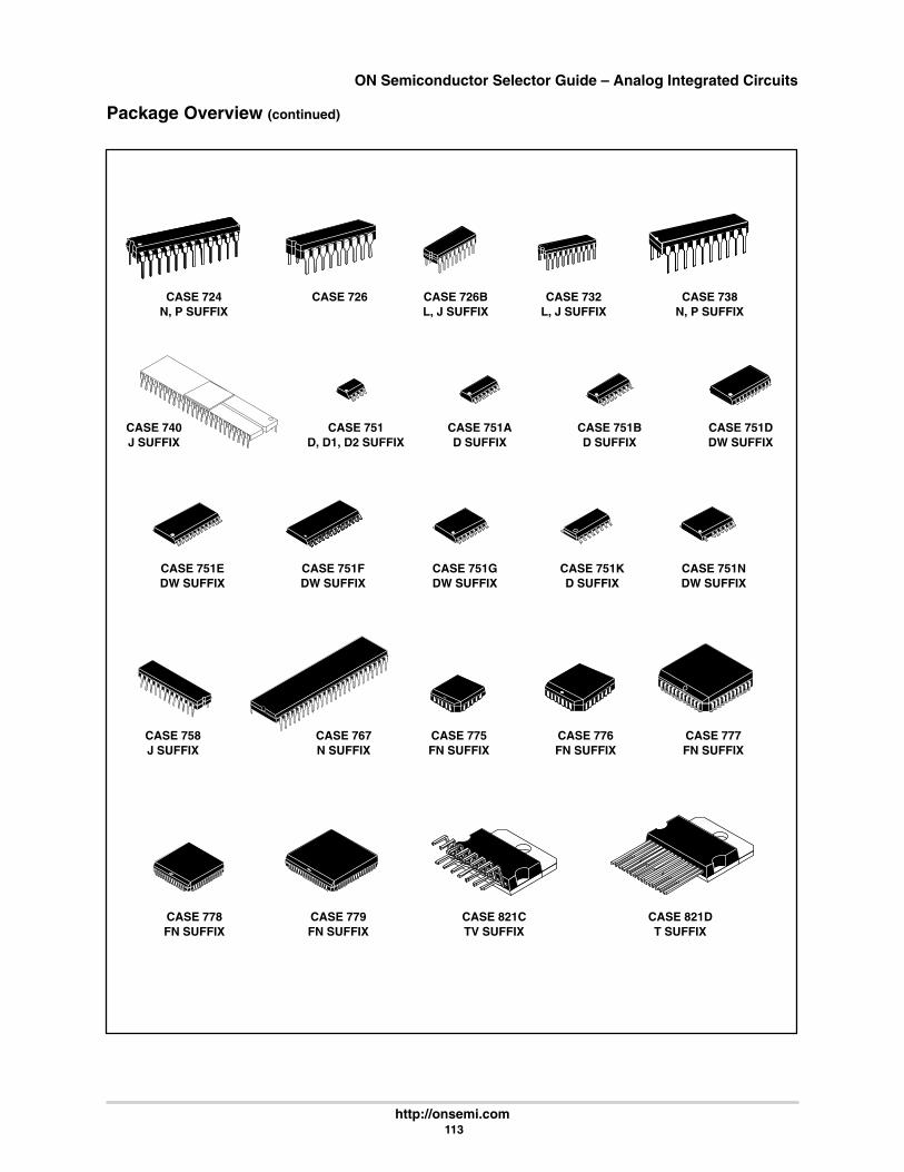
ON Semiconductor Selector Guide – Analog Integrated Circuits
http://onsemi.com 113
Package Overview (continued)
CASE 738N, P SUFFIX
CASE 732L, J SUFFIX
CASE 726BL, J SUFFIX
CASE 726CASE 724N, P SUFFIX
CASE 740J SUFFIX
CASE 751DDW SUFFIX
CASE 751AD SUFFIX
CASE 751BD SUFFIX
CASE 751D, D1, D2 SUFFIX
CASE 751EDW SUFFIX
CASE 751GDW SUFFIX
CASE 751KD SUFFIX
CASE 751FDW SUFFIX
CASE 751NDW SUFFIX
CASE 758J SUFFIX
CASE 767N SUFFIX
CASE 775FN SUFFIX
CASE 777FN SUFFIX
CASE 776FN SUFFIX
CASE 821CTV SUFFIX
CASE 821DT SUFFIX
CASE 778FN SUFFIX
CASE 779FN SUFFIX

ON Semiconductor Selector Guide – Analog Integrated Circuits
http://onsemi.com 114
Package Overview (continued)
CASE 842DFU SUFFIX
CASE 846ADM SUFFIX
CASE 848DFA, FB SUFFIX
CASE 873AFA, FB SUFFIX
CASE 904F SUFFIX
CASE 932FTA SUFFIX
CASE 936D2T SUFFIX
CASE 936AD2T SUFFIX
CASE 940BSD SUFFIX
CASE 940JVF SUFFIX
CASE 948EDT, DTB SUFFIX
CASE 948FDT, DTB SUFFIX
CASE 948GDT, DTB SUFFIX
CASE 948HDT, DTB SUFFIX
CASE 1212N SUFFIX
CASE 1213H SUFFIX
CASE 940SD SUFFIX
CASE 965M SUFFIX
CASE 940ASD SUFFIX
CASE 966M SUFFIX
CASE 967M SUFFIX
CASE 940CSD SUFFIX
CASE 940DSD SUFFIX
CASE 1201DT SUFFIX
CASE 1202DT SUFFIX
ON Semiconductor Selector Guide – Logic Devices
http://onsemi.com 115
Logic Devices
In Brief . . .Page
Selection by FunctionLogic Functions 116. . . . . . . . . . . . . . . . . . . . . . . . . . .
Device Index 134. . . . . . . . . . . . . . . . . . . . . . . . . . . . . . . . . Ordering Information 139. . . . . . . . . . . . . . . . . . . . . . . . . . Packaging Information 142. . . . . . . . . . . . . . . . . . . . . . . .
Surface Mount 142. . . . . . . . . . . . . . . . . . . . . . . . . . . . Pin Conversion Tables 142. . . . . . . . . . . . . . . . . . . . . . Tape and Reel 143. . . . . . . . . . . . . . . . . . . . . . . . . . . . .
This selector guide is a quick reference toON Semiconductor’s vast offering of standard logicintegrated circuits. In TTL, popular due to its ease of use,low cost, medium–to–high speed operation and goodoutput drive capability, ON Semiconductor offers LS.ON Semiconductor’s CMOS portfolio includesMC14000B standard CMOS series devices,High–Speed CMOS consisting of a full line of productsthat are pinout– compatible with many LSTTL andMC14000B standard CMOS logic devices which offersdesigners a solution to the long–standing combinedbarrier — high speed and low power. ON Semiconductoralso offers a several new advanced lines of CMOS whichinclude low–voltage, voltage tolerance and veryhigh–speed features (LVX, LCX, VCX, VHC andVHCT) consisting of the most commonly used CMOSproducts. ON Semiconductor’s Emitter Coupled Logic(MECL) is a non–saturated form of digital logic whicheliminates transistor storage time permitting very highspeed operation. ON Semiconductor offers a widevariety of MECL: MECL 10K; MECL 10H; ECLinPS(ECL in picoseconds); ECLinPS Lite; Low–VoltageECLinPS and ECLinPS Lite; and ECLinPS andLow–Voltage ECLinPS level translation. Also availableis ECLinPS Plus, a recently introduced higherperformance family of ECLinPS products. Timingsolution products such as clock drivers, clock generatorsand programmable delay chips are also included. Highperformance and communications products such asVCO’s, a wide variety of translators, low–voltage businterface and serial data transmission devices are alsoavailable.

ON Semiconductor Selector Guide – Logic Devices
http://onsemi.com 116
Selection by Function
In order to better serve our customers, we have made some modifications to the Selection by Function portion of theLogic Selector Guide. For easy selection of Logic’s newer, more complex functions, as well as standard family functions,refer to the subject index below. Within the Selection by Function tables you will find functions sorted by these broadsubjects, and then broken down alphabetically into more precise functions.
Logic Functions
AMPLIFIER 117. . . . . . . . . . . . . . . . . . . . . . . . . . . . . . . ARITHMETIC OPERATORS 117. . . . . . . . . . . . . . . . BOUNCE ELIMINATOR 117. . . . . . . . . . . . . . . . . . . . BUFFERS 117. . . . . . . . . . . . . . . . . . . . . . . . . . . . . . . . BUFFERS, 3–STATE 117. . . . . . . . . . . . . . . . . . . . . . . BUS INTERFACE 118. . . . . . . . . . . . . . . . . . . . . . . . . . CBM 119. . . . . . . . . . . . . . . . . . . . . . . . . . . . . . . . . . . . . CLOCK DISTRIBUTION CHIPS 119. . . . . . . . . . . . . CLOCK DRIVERS 119. . . . . . . . . . . . . . . . . . . . . . . . . COAX CABLE DRIVERS 119. . . . . . . . . . . . . . . . . . . COMPARATORS 119. . . . . . . . . . . . . . . . . . . . . . . . . . CONVERTERS 120. . . . . . . . . . . . . . . . . . . . . . . . . . . . COUNTERS 120. . . . . . . . . . . . . . . . . . . . . . . . . . . . . . DECODERS 121. . . . . . . . . . . . . . . . . . . . . . . . . . . . . . DECODER/DEMULTIPLEXERS 121. . . . . . . . . . . . . DISPLAY DECODE DRIVERS 121. . . . . . . . . . . . . . . DIVIDERS 122. . . . . . . . . . . . . . . . . . . . . . . . . . . . . . . . DRIVER 122. . . . . . . . . . . . . . . . . . . . . . . . . . . . . . . . . . ENCODERS 122. . . . . . . . . . . . . . . . . . . . . . . . . . . . . . ENCODER/DECODERS 122. . . . . . . . . . . . . . . . . . . . FLIP–FLOPS 122. . . . . . . . . . . . . . . . . . . . . . . . . . . . . . GATES, AND/NAND 124. . . . . . . . . . . . . . . . . . . . . . . GATES, COMPLEX 125. . . . . . . . . . . . . . . . . . . . . . . .
GATES, EXCLUSIVE OR/EXCLUSIVE NOR 125. . GATES, NOR 126. . . . . . . . . . . . . . . . . . . . . . . . . . . . . GATES, OR 126. . . . . . . . . . . . . . . . . . . . . . . . . . . . . . . INVERTERS 127. . . . . . . . . . . . . . . . . . . . . . . . . . . . . . INVERTER/BUFFERS, 2–STATE 127. . . . . . . . . . . . LATCHES 127. . . . . . . . . . . . . . . . . . . . . . . . . . . . . . . . MISCELLANEOUS 128. . . . . . . . . . . . . . . . . . . . . . . . MULTIPLEXERS 128. . . . . . . . . . . . . . . . . . . . . . . . . . MULTIPLEXER/DATA SELECTORS 128. . . . . . . . . . MULTIVIBRATORS 130. . . . . . . . . . . . . . . . . . . . . . . . OSCILLATOR/TIMERS 130. . . . . . . . . . . . . . . . . . . . . PARITY CHECKERS 130. . . . . . . . . . . . . . . . . . . . . . . PHASE–LOCKED LOOP 130. . . . . . . . . . . . . . . . . . . PROGRAMMABLE DELAY CHIPS 130. . . . . . . . . . . RECEIVERS 130. . . . . . . . . . . . . . . . . . . . . . . . . . . . . . REGISTERS 131. . . . . . . . . . . . . . . . . . . . . . . . . . . . . . REGISTER FILES 131. . . . . . . . . . . . . . . . . . . . . . . . . SCHMITT TRIGGERS 131. . . . . . . . . . . . . . . . . . . . . . SHIFT REGISTERS 131. . . . . . . . . . . . . . . . . . . . . . . . TRANSCEIVERS 132. . . . . . . . . . . . . . . . . . . . . . . . . . TRANSLATORS 133. . . . . . . . . . . . . . . . . . . . . . . . . . . VCO 133. . . . . . . . . . . . . . . . . . . . . . . . . . . . . . . . . . . . .

ON Semiconductor Selector Guide – Logic Devices
http://onsemi.com 117
Selection by Function
Description Tech. Device(s) Pins DIP SM
AMPLIFIER
Fiber Optic Post Amplifier ECL MC10SX1125 – 16 D
ARITHMETIC OPERATORS
4–Bit Arithmetic Logic Unit/Function Generator ECL MC10H181 – 24 P,L,PW,LW
FN
4–Bit Binary Full Adder With Fast Carry TTL SN74LS283 – 16 N,J D
4–Bit Full Adder CMOS MC14008B – 16 P,L D
Dual 2–Bit Adder/Subtractor ECL MC10H180 – 16 P,L FN
Look Ahead Carry Block ECL MC10H179 – 16 P,L FN
BOUNCE ELIMINATOR
Hex Contact Bounce Eliminator CMOS MC14490 – 16 P,L DW
BUFFERS
1:2 Differential Fanout Buffer ECL MC100LVEL11 – 8 D
ECL MC10EL11 MC100EL11 8 D
2:8 Differential Fanout Buffer ECL MC100LVE310 MC100E310 28 FN
Dual 1:3 Fanout Buffer ECL MC100LVEL13 MC100EL13 20 DW
Low Voltage Dual 1:4, 1:5 Differential Fanout Buffer,ECL/PECL Compatible
ECL MC100LVE210 MC100E210 28 FN
Octal Bus Buffer Inverting CMOS MC74VHC540 – 20 DW,DT,M
Quad Bus Buffer With 5V–Tolerant Inputs CMOS MC74LVX125 – 14 D,DT,M
Quad Bus Buffer With 3–State Control Inputs CMOS MC74VHC126 – 14 D,DT,M
BUFFERS, 3–STATE
Low–Voltage CMOS 16–Bit Buffer, 3–State, InvertingWith 5V Tolerant Inputs and Outputs
CMOS MC74LCX16240A – 20 DW,M,DT
CMOS MC74LCX16240 – 48 DT
Low–Voltage CMOS 16–Bit Buffer, 3–State,Non–Inverting With 5V Tolerant Inputs and Outputs
CMOS MC74LCX16244 – 20 DW,M,DT
Low–Voltage CMOS Octal Buffer, 3–State, Non–InvertingWith 5V Tolerant Inputs and Outputs
CMOS MC74LCX244 – 20 DW,M,DT
Low–Voltage CMOS Octal Buffer, 3–State, Inverting With5V Tolerant Inputs and Outputs
CMOS MC74LCX240 – 20 DW,M,DT
Low–Voltage CMOS Octal Buffer Flow Through Pinout,3–State, Non–Inverting With 5V Tolerant Inputs and Outputs
CMOS MC74LCX541 – 20 DW,M,DT
Low–Voltage CMOS Octal Buffer Flow Through Pinout,3–State, Inverting With 5V Tolerant Inputs and Outputs
CMOS MC74LCX540 – 20 DW,M,DT
Low–Voltage CMOS Quad Buffer, 3–State, Inverting With5V Tolerant Inputs and Outputs
CMOS MC74LCX125 – 20 DW,M,DT
Octal Bus Buffer Inverting With 5V–Tolerant Inputs CMOS MC74LVX240 – 20 DW,DT,M
Octal Bus Buffer Non–Inverting 3–State Buffer/LineDriver/Line Receiver
CMOS MC74VHCT541A – 20 DW,DT,M
Octal Bus Buffer Non–Inverting With 5V–Tolerant Inputs CMOS MC74LVX244 – 20 DW,DT,M
Octal Bus Buffer/Line Driver Inverting With 3–StateOutputs
CMOS MC74VHC240 – 20 DW,DT,M
Octal Bus Buffer/Line Driver Inverting With 3–StateOutputs
CMOS MC74VHCT240A – 20 DW,DT,M
Octal Bus Buffer/Line Driver Non–Inverting With 3–StateOutputs
CMOS MC74VHCT244A – 20 DW,DT,M

ON Semiconductor Selector Guide – Logic Devices
http://onsemi.com 118
Selection by Function
Description SMDIPPinsDevice(s)Tech.
BUFFERS, 3–STATE
Quad 3–State Non–Inverting Buffer CMOS MC74HC126 – 14 N D,DT
BUS INTERFACE
Dual Bus Driver/Receiver With 4–to–1 Output Multiplexer(25Ω)
ECL MC10H332 – 20 P,L FN
Hex Buffer 4/2–Bit/Inverting With 3–State Outputs TTL SN74LS368A – 16 N,J D
Hex Buffer 4/2–Bit/Non–Inverting With 3–State Outputs TTL SN74LS367A – 16 N,J D
Hex Buffer Gated Enable Non–Inverting With 3–StateOutputs
TTL SN74LS365A – 16 N,J D
Hex With 3–State Outputs Buffer (Non–Inverting) CMOS MC14503B – 16 P,L D
Octal 3–State Non–Inverting Bus Transceiver WithLSTTL Compatible Inputs
CMOS MC74HCT245A – 20 N,J DW,SD,DT
Octal Bidirectional Transceiver With 3–StateInputs/Outputs
CMOS MC74AC245 – 20 N DW
CMOS MC74ACT245 – 20 N DW
Octal Bidirectional Transceiver With 3–State Outputs CMOS MC74ACT640 – 20 N DW
Octal Buffer/Line Driver With 3–State Outputs TTL SN74LS244 – 20 N,J DW
TTL SN74LS240 – 20 N,J DW
TTL SN74LS541 – 20 N,J DW
CMOS MC74AC244 – 20 N DW
CMOS MC74ACT244 – 20 N DW
CMOS MC74AC540 – 20 N DW
CMOS MC74ACT540 – 20 N DW
CMOS MC74AC541 – 20 N DW
CMOS MC74ACT541 – 20 N DW
CMOS MC74AC240 – 20 N DW
CMOS MC74ACT240 – 20 N DW
CMOS MC74ACT241 – 20 N DW
Octal Bus Transceiver TTL SN74LS245 – 20 N,J DW
Octal Bus Transceiver/Inverting With 3–State Outputs TTL SN74LS640 – 20 N,J DW
Octal Bus Transceiver/Register With 3–State OutputsNon–Inverting
CMOS MC74AC652 – 24 N DW
CMOS MC74ACT652 – 24 N DW
Octal Transceiver/Register With 3–State OutputsNon–Inverting
CMOS MC74AC646 – 24 N DW
CMOS MC74ACT646 – 24 N DW
Octal With 3–State Non–Inverting Buffer/Line Driver/LineReceiver With LSTTL Compatible Inputs
CMOS MC74HCT244A – 20 N,J DW,SD,DT
Octal With 3–State Outputs Inverting Buffer/LineDriver/Line Receiver
CMOS MC74HC240A – 20 N,J DW,DT
CMOS MC74HC540A – 20 N,J DW
Octal With 3–State Outputs Non–Inverting Buffer/LineDriver/Line Receiver
CMOS MC74HC541A – 20 N,J DW
CMOS MC74VHC541 – 20 DW,DT,M
Octal With 3–State Outputs Non–Inverting Buffer/LineDriver/Line Receiver With LSTTL Compatible Inputs
CMOS MC74HCT541A – 20 N DW
Octal With 3–State Outputs Non–Inverting Buffer/LineDriver/Line Receiver
CMOS MC74HC244A – 20 N,J DW,SD,DT
CMOS MC74VHC244 – 20 DW,DT,M
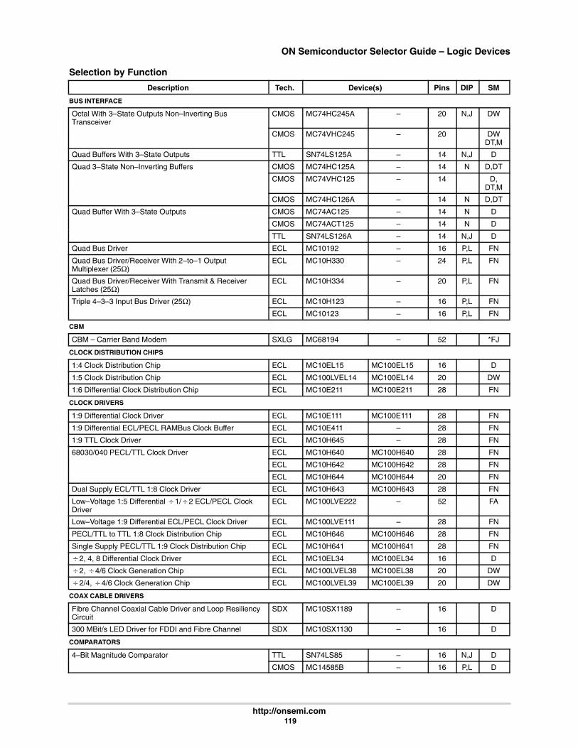
ON Semiconductor Selector Guide – Logic Devices
http://onsemi.com 119
Selection by Function
Description SMDIPPinsDevice(s)Tech.
BUS INTERFACE
Octal With 3–State Outputs Non–Inverting BusTransceiver
CMOS MC74HC245A – 20 N,J DW
CMOS MC74VHC245 – 20 DWDT,M
Quad Buffers With 3–State Outputs TTL SN74LS125A – 14 N,J D
Quad 3–State Non–Inverting Buffers CMOS MC74HC125A – 14 N D,DT
CMOS MC74VHC125 – 14 D,DT,M
CMOS MC74HC126A – 14 N D,DT
Quad Buffer With 3–State Outputs CMOS MC74AC125 – 14 N D
CMOS MC74ACT125 – 14 N D
TTL SN74LS126A – 14 N,J D
Quad Bus Driver ECL MC10192 – 16 P,L FN
Quad Bus Driver/Receiver With 2–to–1 OutputMultiplexer (25Ω)
ECL MC10H330 – 24 P,L FN
Quad Bus Driver/Receiver With Transmit & ReceiverLatches (25Ω)
ECL MC10H334 – 20 P,L FN
Triple 4–3–3 Input Bus Driver (25Ω) ECL MC10H123 – 16 P,L FN
ECL MC10123 – 16 P,L FN
CBM
CBM – Carrier Band Modem SXLG MC68194 – 52 *FJ
CLOCK DISTRIBUTION CHIPS
1:4 Clock Distribution Chip ECL MC10EL15 MC100EL15 16 D
1:5 Clock Distribution Chip ECL MC100LVEL14 MC100EL14 20 DW
1:6 Differential Clock Distribution Chip ECL MC10E211 MC100E211 28 FN
CLOCK DRIVERS
1:9 Differential Clock Driver ECL MC10E111 MC100E111 28 FN
1:9 Differential ECL/PECL RAMBus Clock Buffer ECL MC10E411 – 28 FN
1:9 TTL Clock Driver ECL MC10H645 – 28 FN
68030/040 PECL/TTL Clock Driver ECL MC10H640 MC100H640 28 FN
ECL MC10H642 MC100H642 28 FN
ECL MC10H644 MC100H644 20 FN
Dual Supply ECL/TTL 1:8 Clock Driver ECL MC10H643 MC100H643 28 FN
Low–Voltage 1:5 Differential 1/2 ECL/PECL ClockDriver
ECL MC100LVE222 – 52 FA
Low–Voltage 1:9 Differential ECL/PECL Clock Driver ECL MC100LVE111 – 28 FN
PECL/TTL to TTL 1:8 Clock Distribution Chip ECL MC10H646 MC100H646 28 FN
Single Supply PECL/TTL 1:9 Clock Distribution Chip ECL MC10H641 MC100H641 28 FN
2, 4, 8 Differential Clock Driver ECL MC10EL34 MC100EL34 16 D
2, 4/6 Clock Generation Chip ECL MC100LVEL38 MC100EL38 20 DW
2/4, 4/6 Clock Generation Chip ECL MC100LVEL39 MC100EL39 20 DW
COAX CABLE DRIVERS
Fibre Channel Coaxial Cable Driver and Loop ResiliencyCircuit
SDX MC10SX1189 – 16 D
300 MBit/s LED Driver for FDDI and Fibre Channel SDX MC10SX1130 – 16 D
COMPARATORS
4–Bit Magnitude Comparator TTL SN74LS85 – 16 N,J D
CMOS MC14585B – 16 P,L D
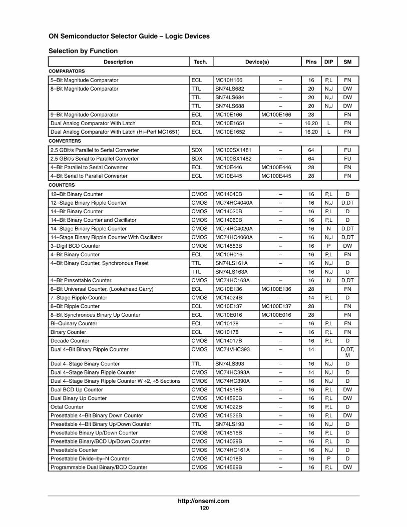
ON Semiconductor Selector Guide – Logic Devices
http://onsemi.com 120
Selection by Function
Description SMDIPPinsDevice(s)Tech.
COMPARATORS
5–Bit Magnitude Comparator ECL MC10H166 – 16 P,L FN
8–Bit Magnitude Comparator TTL SN74LS682 – 20 N,J DW
TTL SN74LS684 – 20 N,J DW
TTL SN74LS688 – 20 N,J DW
9–Bit Magnitude Comparator ECL MC10E166 MC100E166 28 FN
Dual Analog Comparator With Latch ECL MC10E1651 – 16,20 L FN
Dual Analog Comparator With Latch (Hi–Perf MC1651) ECL MC10E1652 – 16,20 L FN
CONVERTERS
2.5 GBit/s Parallel to Serial Converter SDX MC100SX1481 – 64 FU
2.5 GBit/s Serial to Parallel Converter SDX MC100SX1482 – 64 FU
4–Bit Parallel to Serial Converter ECL MC10E446 MC100E446 28 FN
4–Bit Serial to Parallel Converter ECL MC10E445 MC100E445 28 FN
COUNTERS
12–Bit Binary Counter CMOS MC14040B – 16 P,L D
12–Stage Binary Ripple Counter CMOS MC74HC4040A – 16 N,J D,DT
14–Bit Binary Counter CMOS MC14020B – 16 P,L D
14–Bit Binary Counter and Oscillator CMOS MC14060B – 16 P,L D
14–Stage Binary Ripple Counter CMOS MC74HC4020A – 16 N D,DT
14–Stage Binary Ripple Counter With Oscillator CMOS MC74HC4060A – 16 N,J D,DT
3–Digit BCD Counter CMOS MC14553B – 16 P DW
4–Bit Binary Counter ECL MC10H016 – 16 P,L FN
4–Bit Binary Counter, Synchronous Reset TTL SN74LS161A – 16 N,J D
TTL SN74LS163A – 16 N,J D
4–Bit Presettable Counter CMOS MC74HC163A – 16 N D,DT
6–Bit Universal Counter, (Lookahead Carry) ECL MC10E136 MC100E136 28 FN
7–Stage Ripple Counter CMOS MC14024B – 14 P,L D
8–Bit Ripple Counter ECL MC10E137 MC100E137 28 FN
8–Bit Synchronous Binary Up Counter ECL MC10E016 MC100E016 28 FN
Bi–Quinary Counter ECL MC10138 – 16 P,L FN
Binary Counter ECL MC10178 – 16 P,L FN
Decade Counter CMOS MC14017B – 16 P,L D
Dual 4–Bit Binary Ripple Counter CMOS MC74VHC393 – 14 D,DT,M
Dual 4–Stage Binary Counter TTL SN74LS393 – 16 N,J D
Dual 4–Stage Binary Ripple Counter CMOS MC74HC393A – 14 N,J D
Dual 4–Stage Binary Ripple Counter W ÷2, ÷5 Sections CMOS MC74HC390A – 16 N,J D
Dual BCD Up Counter CMOS MC14518B – 16 P,L DW
Dual Binary Up Counter CMOS MC14520B – 16 P,L DW
Octal Counter CMOS MC14022B – 16 P,L D
Presettable 4–Bit Binary Down Counter CMOS MC14526B – 16 P,L DW
Presettable 4–Bit Binary Up/Down Counter TTL SN74LS193 – 16 N,J D
Presettable Binary Up/Down Counter CMOS MC14516B – 16 P,L D
Presettable Binary/BCD Up/Down Counter CMOS MC14029B – 16 P,L D
Presettable Counter CMOS MC74HC161A – 16 N,J D
Presettable Divide–by–N Counter CMOS MC14018B – 16 P D
Programmable Dual Binary/BCD Counter CMOS MC14569B – 16 P,L DW

ON Semiconductor Selector Guide – Logic Devices
http://onsemi.com 121
Selection by Function
Description SMDIPPinsDevice(s)Tech.
COUNTERS
Synchronous Presettable Binary Counter CMOS MC74AC161 – 16 N D
CMOS MC74ACT161 – 16 N D
Synchronous Presettable Binary Counter CMOS MC74AC163 – 16 N D
CMOS MC74ACT163 – 16 N D
Universal Hexadecimal Counter ECL MC10H136 – 16 P,L FN
ECL MC10136 – 16 P,L FN
DECODERS
3–to–8 Line Decoder With 5V–Tolerant Inputs CMOS MC74LVX138 – 16 D,DT,M
3–to–8 Line Decoder CMOS MC74VHCT138A – 16 D,DT,M
CMI Coder/Decoder SDX MC100SX1230 – 28 FN
DECODER/DEMULTIPLEXERS
1–of–10 Decoder TTL SN74LS42 – 16 N,J D
1–of–10 Decoder/Driver Open–Collector TTL SN74LS145 – 16 N,J D
1–of–8 Decoder/Demultiplexer CMOS MC74AC138 – 16 N D
CMOS MC74ACT138 – 16 N D
CMOS MC74HC138A – 16 N,J D
CMOS MC74VHC138 – 16 D,DT,M
CMOS MC74HCT138A – 16 N D,DT
TTL SN74LS138 – 16 N,J D
4–Bit Transparent Latch/4–to–16 Line Decoder (High) CMOS MC14514B – 24 P,L DW
4–Bit Transparent Latch/4–to–16 Line Decoder (Low) CMOS MC14515B – 24 P,L DW
BCD–to–Decimal Decoder/Binary–to–Octal Decoder CMOS MC14028B – 16 P,L D
Binary to 1–4 Decoder (Low) ECL MC10171 – 16 P,L FN
Binary to 1–8 Decoder, (High) ECL MC10H162 – 16 P,L FN
ECL MC10162 – 16 P,L FN
Binary to 1–8 Decoder, (Low) ECL MC10H161 – 16 P,L FN
ECL MC10161 – 16 P,L FN
Dual 1–of–4 Decoder Open–Collector TTL SN74LS156 – 16 N,J D
Dual 1–of–4 Decoder/Demultiplexer CMOS MC74AC139 – 16 N D
CMOS MC74ACT139 – 16 N D
Dual 1–of–4 Decoder/Demultiplexer CMOS MC74HC139A – 16 N,J D
TTL SN74LS139 – 16 N,J D
Dual 2–to–4 Decoder/Demultiplexer CMOS MC74VHC139 – 16 D,DT,M
Dual Binary to 1–4 Decoder (High) ECL MC10H172 – 16 P,L FN
Dual Binary to 1–4 Decoder (Low) ECL MC10H171 – 16 P,L FN
Dual Binary to 1–of–4 Decoder (Active High Outputs) CMOS MC14555B – 16 P D
Dual Binary to 1–of–4 Decoder (Active Low Outputs) CMOS MC14556B – 16 P D
Low–Voltage CMOS 1–of–8 Decoder/Demultiplexer With5V Tolerant Inputs and Outputs
CMOS MC74LCX138 – 16 D,DT
DISPLAY DECODE DRIVERS
BCD–to–Seven Segment Decoder/Driver TTL SN74LS47 – 16 N,J D
TTL SN74LS247 – 16 N,J D
BCD–to–Seven Segment Latch/Decoder/Driver CMOS MC14511B – 16 P,L D,DW

ON Semiconductor Selector Guide – Logic Devices
http://onsemi.com 122
Selection by Function
Description SMDIPPinsDevice(s)Tech.
DISPLAY DECODE DRIVERS
BCD–to–Seven Segment Latch/Decoder/Driver for LiquidCrystals
CMOS MC14543B – 16 P,L D
BCD–to–Seven Segment Latch/Decoder/Driver WithRipple Blanking
CMOS MC14513B – 18 P
DIVIDERS
÷ 2 Divider ECL MC10EL32 MC100EL32 8 D
ECL MC100LVEL32 – 8 D
÷ 4 Divider ECL MC10EL33 MC100EL33 8 D
ECL MC100LVEL33 – 8 D
DRIVER
Coaxial Cable Driver ECL MC10EL89 – 8 D
300MBit/s LED Driver for FDDI and Fibre Channel ECL MC10SX1130 – 16 D
ENCODERS
10–Line to 4–Line Priority Encoder TTL SN74LS147 – 16 N,J D
8–Bit Priority Encoder CMOS MC14532B – 16 P,L D
8–Input Priority Encoder ECL MC10H165 – 16 P,L FN
8–Line to 3–Line Priority Encoder TTL SN74LS148 – 16 N,J D
ENCODER/DECODERS
CMI Encoder/Decoder ECL MC100SX1230 – 28 FN
FLIP–FLOPS
3–Bit Differential Flip–Flop ECL MC10E431 MC100E431 28 FN
4–Bit D–Type Flip–Flop Individual Clock, ResetDifferential Output
ECL MC10E131 MC100E131 28 FN
5–Bit Differential Register ECL MC10E452 MC100E452 28 FN
6–Bit 2:1 Mux–Register With Common Clock,Asynchronous Master Reset Single Ended
ECL MC10E167 MC100E167 28 FN
6–Bit D–Type Register With Common Clock,Asynchronous Master Reset, Differential Outputs
ECL MC10E151 MC100E151 28 FN
6–Bit D–Type Register, With Differential Inputs, (Data &Clock) , VBB, Common Reset
ECL MC10E451 MC100E451 28 FN
9–Bit Hold Register, 700MHz, With Asynchronous MasterReset
ECL MC10E143 MC100E143 28 FN
D–Type Flip–Flop With Set & Reset ECL MC10EL31 MC100EL31 8 D
Differential Clock D–Type Flip–Flop ECL MC10EL51 MC100EL51 8 D
ECL MC100LVEL51 – 8 D
Differential Data & Clock D–Type Flip–Flop ECL MC10EL52 MC100EL52 8 D
Dual D–Type Flip–Flop CMOS MC74AC74 – 14 N D
CMOS MC74ACT74 – 14 N D
CMOS MC14013B – 14 P,L D
Dual D–Type Flip–Flop With Set and Reset CMOS MC74HC74A – 14 N,J D,DT
CMOS MC74VHC74 – 14 D,DT,M
CMOS MC74VHCT74A – 14 D,DT,M
Dual D–Type Flip–Flop With Set and Reset With LSTTLCompatible Inputs
CMOS MC74HCT74A – 14 N D
Dual D–Type Flip–Flop With Set and Clear, With5V–Tolerant Inputs
CMOS MC74LVX74 – 14 D,DT,M
Dual D–Type Positive Edge–Triggered Flip–Flop TTL SN74LS74A – 16 N,J D
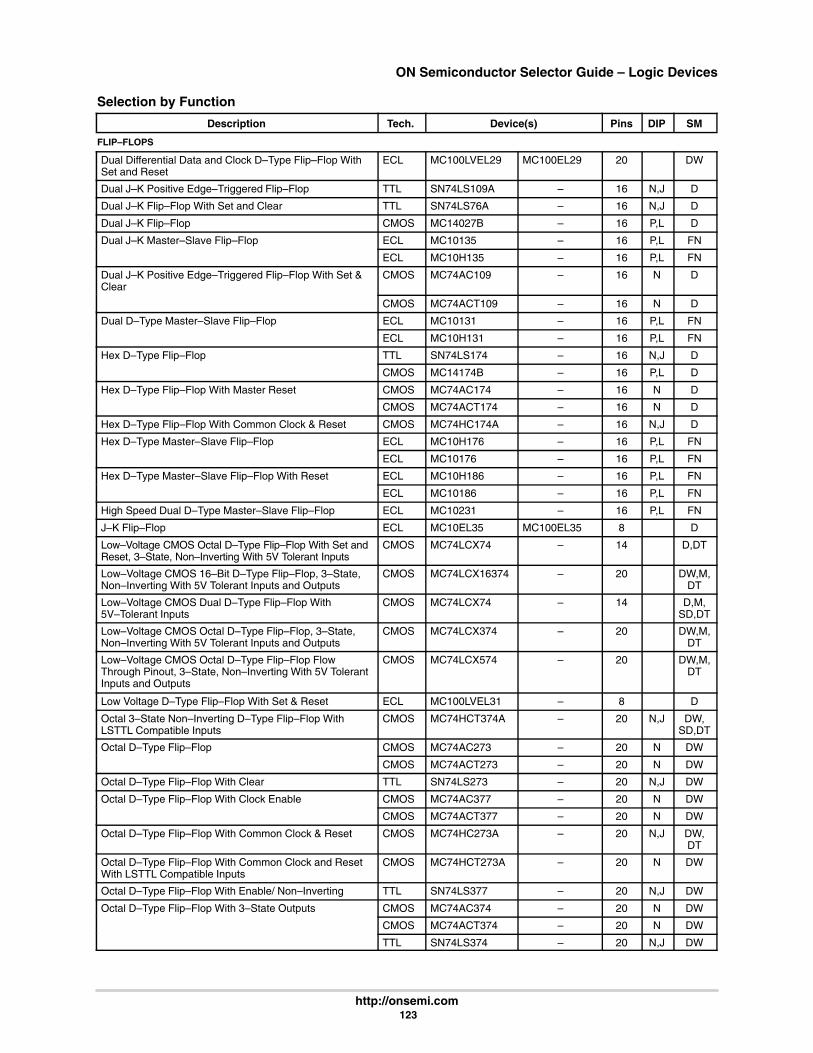
ON Semiconductor Selector Guide – Logic Devices
http://onsemi.com 123
Selection by Function
Description SMDIPPinsDevice(s)Tech.
FLIP–FLOPS
Dual Differential Data and Clock D–Type Flip–Flop WithSet and Reset
ECL MC100LVEL29 MC100EL29 20 DW
Dual J–K Positive Edge–Triggered Flip–Flop TTL SN74LS109A – 16 N,J D
Dual J–K Flip–Flop With Set and Clear TTL SN74LS76A – 16 N,J D
Dual J–K Flip–Flop CMOS MC14027B – 16 P,L D
Dual J–K Master–Slave Flip–Flop ECL MC10135 – 16 P,L FN
ECL MC10H135 – 16 P,L FN
Dual J–K Positive Edge–Triggered Flip–Flop With Set &Clear
CMOS MC74AC109 – 16 N D
CMOS MC74ACT109 – 16 N D
Dual D–Type Master–Slave Flip–Flop ECL MC10131 – 16 P,L FN
ECL MC10H131 – 16 P,L FN
Hex D–Type Flip–Flop TTL SN74LS174 – 16 N,J D
CMOS MC14174B – 16 P,L D
Hex D–Type Flip–Flop With Master Reset CMOS MC74AC174 – 16 N D
CMOS MC74ACT174 – 16 N D
Hex D–Type Flip–Flop With Common Clock & Reset CMOS MC74HC174A – 16 N,J D
Hex D–Type Master–Slave Flip–Flop ECL MC10H176 – 16 P,L FN
ECL MC10176 – 16 P,L FN
Hex D–Type Master–Slave Flip–Flop With Reset ECL MC10H186 – 16 P,L FN
ECL MC10186 – 16 P,L FN
High Speed Dual D–Type Master–Slave Flip–Flop ECL MC10231 – 16 P,L FN
J–K Flip–Flop ECL MC10EL35 MC100EL35 8 D
Low–Voltage CMOS Octal D–Type Flip–Flop With Set andReset, 3–State, Non–Inverting With 5V Tolerant Inputs
CMOS MC74LCX74 – 14 D,DT
Low–Voltage CMOS 16–Bit D–Type Flip–Flop, 3–State,Non–Inverting With 5V Tolerant Inputs and Outputs
CMOS MC74LCX16374 – 20 DW,M,DT
Low–Voltage CMOS Dual D–Type Flip–Flop With5V–Tolerant Inputs
CMOS MC74LCX74 – 14 D,M,SD,DT
Low–Voltage CMOS Octal D–Type Flip–Flop, 3–State,Non–Inverting With 5V Tolerant Inputs and Outputs
CMOS MC74LCX374 – 20 DW,M,DT
Low–Voltage CMOS Octal D–Type Flip–Flop FlowThrough Pinout, 3–State, Non–Inverting With 5V TolerantInputs and Outputs
CMOS MC74LCX574 – 20 DW,M,DT
Low Voltage D–Type Flip–Flop With Set & Reset ECL MC100LVEL31 – 8 D
Octal 3–State Non–Inverting D–Type Flip–Flop WithLSTTL Compatible Inputs
CMOS MC74HCT374A – 20 N,J DW,SD,DT
Octal D–Type Flip–Flop CMOS MC74AC273 – 20 N DW
CMOS MC74ACT273 – 20 N DW
Octal D–Type Flip–Flop With Clear TTL SN74LS273 – 20 N,J DW
Octal D–Type Flip–Flop With Clock Enable CMOS MC74AC377 – 20 N DW
CMOS MC74ACT377 – 20 N DW
Octal D–Type Flip–Flop With Common Clock & Reset CMOS MC74HC273A – 20 N,J DW,DT
Octal D–Type Flip–Flop With Common Clock and ResetWith LSTTL Compatible Inputs
CMOS MC74HCT273A – 20 N DW
Octal D–Type Flip–Flop With Enable/ Non–Inverting TTL SN74LS377 – 20 N,J DW
Octal D–Type Flip–Flop With 3–State Outputs CMOS MC74AC374 – 20 N DW
CMOS MC74ACT374 – 20 N DW
TTL SN74LS374 – 20 N,J DW

ON Semiconductor Selector Guide – Logic Devices
http://onsemi.com 124
Selection by Function
Description SMDIPPinsDevice(s)Tech.
FLIP–FLOPS
Octal D–Type Flip–Flop With 3–State Outputs CMOS MC74VHCT374A – 20 DW,DT,M
CMOS MC74VHCT574A – 20 DW,DT,M
CMOS MC74LVX574 – 20 DW,DT
Octal D–Type Latch With 3–State Outputs CMOS MC74ACT564 – 20 N DW
CMOS MC74AC574 – 20 N DW
CMOS MC74ACT574 – 20 N DW
Octal D–Type Flip–Flop, 3–State Outputs, With5V–Tolerant Inputs
CMOS MC74LVX374 – 20 DW,DT,M
Octal With 3–State Outputs Non–Inverting D–TypeFlip–Flop
CMOS MC74HC374A – 20 N,J DW,SD,DT
CMOS MC74VHC374 – 20 DW,DT,M
CMOS MC74HC574A – 20 N,J DW
CMOS MC74VHC574 – 20 DW,DT,M
Octal With 3–State Outputs Non–Inverting D–TypeFlip–Flop With LSTTL Compatible Inputs
CMOS MC74HCT574A – 20 N,J DW
Quad D–Type Flip–Flop CMOS MC74AC175 – 16 N D
CMOS MC74ACT175 – 16 N D
Quad D–Type Flip–Flop TTL SN74LS175 – 16 N,J D
CMOS MC14175B – 16 P,L D
Quad D–Type Flip–Flop With Common Clock & Reset CMOS MC74HC175 – 16 N,J D
Quad D–Type Register With 3–State Outputs CMOS MC14076B – 16 P,L D
Triple D–Type Flip–Flop With Set and Reset ECL MC100LVEL30 MC100EL30 20 DW
GATES, AND/NAND
Dual 4–Input AND Gate CMOS MC14082B – 14 P,L D
Dual 4–Input NAND Gate CMOS MC74AC20 – 14 N D
CMOS MC74ACT20 – 14 N D
CMOS MC14012B – 14 P,L D
Hex AND Gate ECL MC10197 – 16 P,L FN
Low–Voltage CMOS Quad 2–Input AND Gate,5V–Tolerant Inputs
CMOS MC74LCX08 – 14 D,DT
Low–Voltage CMOS Quad 2–Input NAND Gate,5V–Tolerant Inputs
CMOS MC74LCX00 – 14 D,DT
Quad 2–Input AND Gate CMOS MC74AC08 – 14 N D
CMOS MC74ACT08 – 14 N D
CMOS MC74HC08A – 14 N,J D,DT
CMOS MC74VHC08 – 14 D,DT,M
TTL SN74LS08 – 14 N,J D
ECL MC10H104 – 16 P,L FN
ECL MC10104 – 16 P,L FN
CMOS MC14081B – 14 P,L D
Quad 2–Input AND Gate With 5V–Tolerant Inputs CMOS MC74LVX08 – 14 D,DT,M
Quad 2–Input NAND Buffer Open–Collector TTL SN74LS38 – 14 N,J D
Quad 2–Input NAND Gate CMOS MC74AC00 – 14 N D

ON Semiconductor Selector Guide – Logic Devices
http://onsemi.com 125
Selection by Function
Description SMDIPPinsDevice(s)Tech.
GATES, AND/NAND
Quad 2–Input NAND Gate CMOS MC74ACT00 – 14 N D
CMOS MC74HC00A – 14 N,J D,DT
CMOS MC74VHC00 – 14 D,DT,M
CMOS MC74VHCT00A – 14 D,DT,M
TTL SN74LS00 – 14 N,J D
CMOS MC14011B – 14 P,L D
CMOS MC74VHC00 – 14 D,DT, M
Quad 2–Input NAND Gate (Unbuffered) CMOS MC14011UB – 14 P,L D
Quad 2–Input NAND Gate With 5V–Tolerant Inputs CMOS MC74LVX00 – 14 D,DT,M
Quad 2–Input NAND Gate With Open–Drain Outputs CMOS MC74HC03A – 14 N D,DT
Triple 3–Input AND Gate CMOS MC74AC11 – 14 N D
CMOS MC74ACT11 – 14 N D
CMOS MC14073B – 14 P,L D
Triple 3–Input NAND Gate CMOS MC74AC10 – 14 N D
CMOS MC74ACT10 – 14 N D
CMOS MC14023B – 14 P,L D
GATES, COMPLEX
2–Input AND/NAND Gate ECL MC10EL04 MC100EL04 8 D
2–Input Differential AND/NAND Gate ECL MC10EL05 MC100EL05 8 D
ECL MC100LVEL05 – 8 D
2–Input XOR/NOR Gate ECL MC10EL07 MC100EL07 8 D
4–Input OR/NOR Gate ECL MC10EL01 MC100EL01 8 D
ECL MC100LVEL01 – 8 D
4–Wide OR–AND/OR–AND–Invert Gate ECL MC10H121 – 16 P,L FN
4–Wide OR–AND/OR–AND–Invert Gate ECL MC10121 – 16 P,L FN
Dual 2–Wide 2–3–Input OR–AND/OR–AND–Invert Gate ECL MC10117 – 16 P,L FN
ECL MC10H117 – 16 P,L FN
Dual 4–5 Input OR/NOR Gate ECL MC10H109 – 16 P,L FN
ECL MC10109 – 16 P,L FN
ECL MC10H209 – 16 P,L FN
Hex NAND/NOR/Invert Gate (Unbuffered) CMOS MC14572UB – 16 P D
Quad 4–Input OR/NOR Gate ECL MC10E101 MC100E101 28 FN
Quad Differential AND/NAND Gate ECL MC10E404 MC100E404 28 FN
Quad OR/NOR Gate ECL MC10H101 – 16 P,L FN
ECL MC10101 – 16 P,L FN
Quint 2–Input AND/NAND Gate ECL MC10E104 MC100E104 28 FN
Quint 2–Input XOR/XNOR Gate ECL MC10E107 MC100E107 28 FN
Triple 2–3–2 Input OR/NOR Gate ECL MC10H105 – 16 P,L FN
ECL MC10105 – 16 P,L FN
Triple 2–Input Exclusive OR/Exclusive NOR Gate ECL MC10H107 – 16 P,L FN
ECL MC10107 – 16 P,L FN
GATES, EXCLUSIVE OR/EXCLUSIVE NOR
Low–Voltage CMOS Quad 2–Input Exclusive OR GateWith 5V–Tolerant Inputs
CMOS MC74LCX86 – 14 D,MSD,DT

ON Semiconductor Selector Guide – Logic Devices
http://onsemi.com 126
Selection by Function
Description SMDIPPinsDevice(s)Tech.
GATES, EXCLUSIVE OR/EXCLUSIVE NOR
Quad Exclusive NOR Gate CMOS MC14077B – 14 P,L D
Quad 2–Input Exclusive OR Gate CMOS MC74AC86 – 14 N D
CMOS MC74ACT86 – 14 N D
CMOS MC74VHC86 – 14 D,DT,M
CMOS MC74HC86A – 14 N,J D,DT
Quad 2–Input Exclusive OR Gate With 5V–TolerantInputs
CMOS MC74LVX86 – 14 D,DT,M
Quad Exclusive OR Gate TTL SN74LS86 – 14 N,J D
ECL MC10H113 – 16 P,L FN
ECL MC10113 – 16 P,L FN
CMOS MC14070B – 14 P,L D
GATES, NOR
Dual 3–Input 3–Output NOR Gate ECL MC10H211 – 16 P,L FN
Dual 5–Input NOR Gate TTL SN74LS260 – 14 N,J D
Low–Voltage CMOS Quad 2–Input NOR Gate,5V–Tolerant Inputs
CMOS MC74LCX02 – 14 D,DT
Quad 2–Input NOR Gate CMOS MC74AC02 – 14 N D
CMOS MC74ACT02 – 14 N D
CMOS MC74HC02A – 14 N,J D,DT
CMOS MC74VHC02 – 14 D,DT,M
ECL MC10H102 – 16 P,L FN
ECL MC10102 – 16 P,L FN
CMOS MC14001B – 14 P,L D
Quad 2–Input NOR Gate (Unbuffered) CMOS MC14001UB – 14 P,L D
Quad 2–Input NOR Gate With 5V–Tolerant Inputs CMOS MC74LVX02 – 14 D,DT,M
Quad 2–Input NOR Gate With strobe ECL MC10H100 – 16 P,L FN
Triple 3–Input NOR Gate CMOS MC14025B – 14 P,L D
Triple 4–3–3 Input NOR Gate ECL MC10H106 – 16 P,L FN
ECL MC10106 – 16 P,L FN
GATES, OR
Dual 3–Input 3–Output OR Gate ECL MC10H210 – 16 P,L FN
Low–Voltage CMOS Quad 2–Input OR Gate, 5V–TolerantInputs
CMOS MC74LCX32 – 14 D,DT
Quad 2–Input OR Gate CMOS MC74AC32 – 14 N D
CMOS MC74ACT32 – 14 N D
CMOS MC74HC32A – 14 N,J D,DT
CMOS MC74VHC32 – 14 D,DT,M
TTL SN74LS32 – 14 N,J D
ECL MC10H103 – 16 P,L FN
ECL MC10103 – 16 P,L FN
CMOS MC14071B – 14 P,L D
Quad 2–Input OR Gate With 5V–Tolerant Inputs CMOS MC74LVX32 – 14 D,DT,M
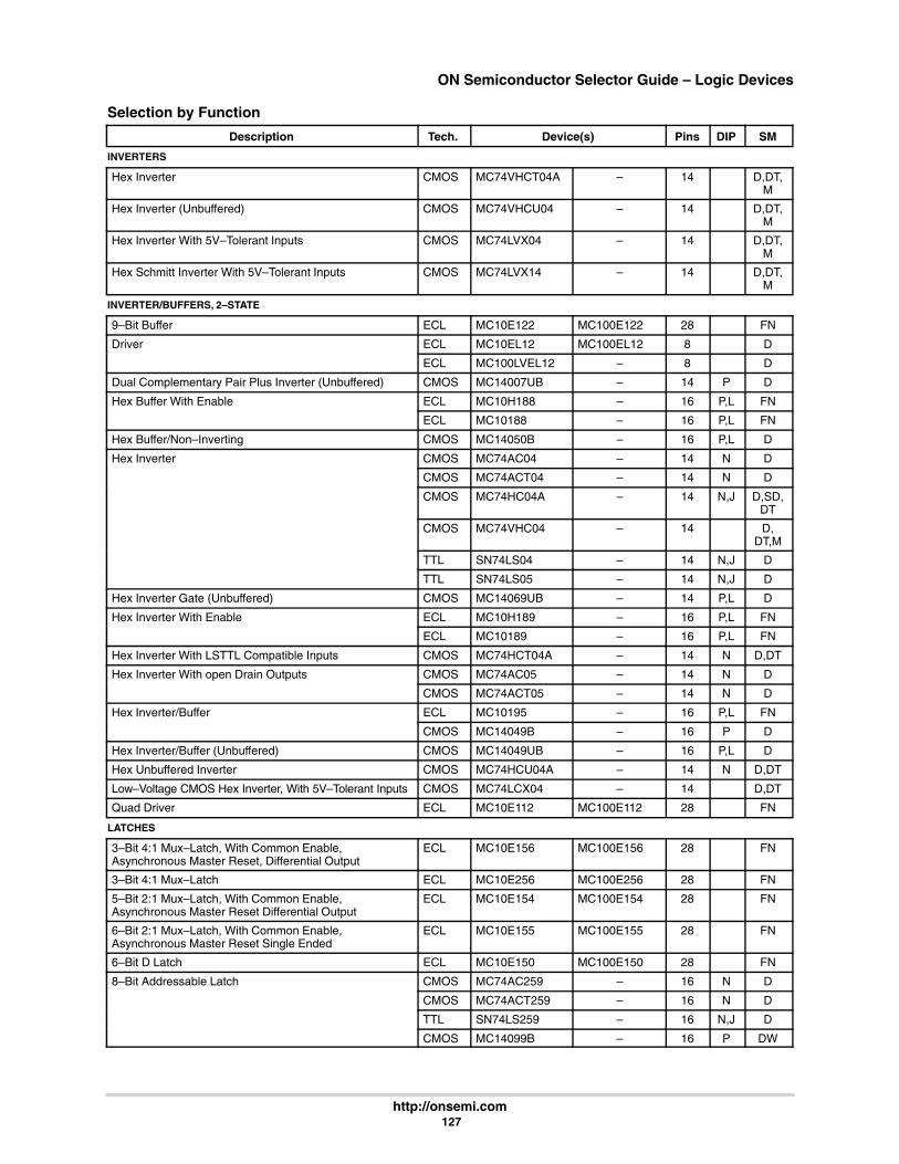
ON Semiconductor Selector Guide – Logic Devices
http://onsemi.com 127
Selection by Function
Description SMDIPPinsDevice(s)Tech.
INVERTERS
Hex Inverter CMOS MC74VHCT04A – 14 D,DT,M
Hex Inverter (Unbuffered) CMOS MC74VHCU04 – 14 D,DT,M
Hex Inverter With 5V–Tolerant Inputs CMOS MC74LVX04 – 14 D,DT,M
Hex Schmitt Inverter With 5V–Tolerant Inputs CMOS MC74LVX14 – 14 D,DT,M
INVERTER/BUFFERS, 2–STATE
9–Bit Buffer ECL MC10E122 MC100E122 28 FN
Driver ECL MC10EL12 MC100EL12 8 D
ECL MC100LVEL12 – 8 D
Dual Complementary Pair Plus Inverter (Unbuffered) CMOS MC14007UB – 14 P D
Hex Buffer With Enable ECL MC10H188 – 16 P,L FN
ECL MC10188 – 16 P,L FN
Hex Buffer/Non–Inverting CMOS MC14050B – 16 P,L D
Hex Inverter CMOS MC74AC04 – 14 N D
CMOS MC74ACT04 – 14 N D
CMOS MC74HC04A – 14 N,J D,SD,DT
CMOS MC74VHC04 – 14 D,DT,M
TTL SN74LS04 – 14 N,J D
TTL SN74LS05 – 14 N,J D
Hex Inverter Gate (Unbuffered) CMOS MC14069UB – 14 P,L D
Hex Inverter With Enable ECL MC10H189 – 16 P,L FN
ECL MC10189 – 16 P,L FN
Hex Inverter With LSTTL Compatible Inputs CMOS MC74HCT04A – 14 N D,DT
Hex Inverter With open Drain Outputs CMOS MC74AC05 – 14 N D
CMOS MC74ACT05 – 14 N D
Hex Inverter/Buffer ECL MC10195 – 16 P,L FN
CMOS MC14049B – 16 P D
Hex Inverter/Buffer (Unbuffered) CMOS MC14049UB – 16 P,L D
Hex Unbuffered Inverter CMOS MC74HCU04A – 14 N D,DT
Low–Voltage CMOS Hex Inverter, With 5V–Tolerant Inputs CMOS MC74LCX04 – 14 D,DT
Quad Driver ECL MC10E112 MC100E112 28 FN
LATCHES
3–Bit 4:1 Mux–Latch, With Common Enable,Asynchronous Master Reset, Differential Output
ECL MC10E156 MC100E156 28 FN
3–Bit 4:1 Mux–Latch ECL MC10E256 MC100E256 28 FN
5–Bit 2:1 Mux–Latch, With Common Enable,Asynchronous Master Reset Differential Output
ECL MC10E154 MC100E154 28 FN
6–Bit 2:1 Mux–Latch, With Common Enable,Asynchronous Master Reset Single Ended
ECL MC10E155 MC100E155 28 FN
6–Bit D Latch ECL MC10E150 MC100E150 28 FN
8–Bit Addressable Latch CMOS MC74AC259 – 16 N D
CMOS MC74ACT259 – 16 N D
TTL SN74LS259 – 16 N,J D
CMOS MC14099B – 16 P DW

ON Semiconductor Selector Guide – Logic Devices
http://onsemi.com 128
Selection by Function
Description SMDIPPinsDevice(s)Tech.
LATCHES
8–Bit Bus Compatible Addressable Latch CMOS MC14598B – 18 P,L
9–Bit Latch, With Parity ECL MC10E175 MC100E175 28 FN
Dual Latch ECL MC10H130 – 16 P,L FN
Low–Voltage CMOS Octal Transparent Latch, 3–State,Non–Inverting With 5V–Tolerant Inputs and Outputs
CMOS MC74LCX373 – 20 DW,M,DT
Low–Voltage CMOS 16–Bit Transparent Latch, 3–State,Non–Inverting With 5V–Tolerant Inputs and Outputs
CMOS MC74LCX16373 – 48 DT
Low–Voltage CMOS Octal Transparent Latch FlowThrough Pinout, 3–State, Non–Inverting With 5V–TolerantInputs and Outputs
CMOS MC74LCX573 – 20 DW,M,SD,DT
Octal 3–State Non–Inverting Transparent Latch WithLSTTL Compatible Inputs
CMOS MC74HCT373A – 20 N,J DW,SD,DT
Octal D–Type Latch With 3–State Outputs CMOS MC74AC573 – 20 N DW
CMOS MC74ACT573 – 20 N DW
CMOS MC74VHCT373A – 20 DW,DT,M
CMOS MC74VHCT573A – 20 DW,DT,M
Octal D–Type Latch, 3–State Outputs, With 5V–TolerantInputs
CMOS MC74LVX373 – 20 DW,DT,M
CMOS MC74LVX573 – 20 DW,DT,M
Octal Transparent Latch With 3–State Outputs CMOS MC74AC373 – 20 N DW
CMOS MC74ACT373 – 20 N DW
TTL SN74LS373 – 20 N,J DW
Octal With 3–State Outputs Non–Inverting TransparentLatch
CMOS MC74HC373A – 20 N,J DW,DT,SD
CMOS MC74VHC373 – 20 DW,DT,M
CMOS MC74HC573A – 20 N,J DW
CMOS MC74VHC573 – 20 DW,DT,M
Octal With 3–State Outputs Non–Inverting TransparentLatch With LSTTL Compatible Inputs
CMOS MC74HCT573A – 20 N DW
Quad Latch ECL MC10153 – 16 P,L FN
Quad NAND R–S Latch CMOS MC14044B – 16 P D
Quad NOR R–S Latch CMOS MC14043B – 16 P,L D
Quad Transparent Latch CMOS MC14042B – 16 P,L D
Quint Latch ECL MC10H175 – 16 P,L FN
ECL MC10175 – 16 P,L FN
MISCELLANEOUS
Data Separator ECL MC10E197 – 28 FN
MULTIPLEXERS
Analog Multiplexer/DemultiplexerHigh Performance Silicon–Gate CMOS
CMOS MC74VHC4051 – 16 D, DT
Low–Voltage CMOS Quad 2–Input Multiplexer CMOS MC74LCX257 – 16 D,M,SD,DT
Quad 2–Channel Multiplexer With 5V–Tolerant Inputs CMOS MC74LVX157 – 16 D,DT,M
MULTIPLEXER/DATA SELECTORS
1–of–8 Decoder/Demultiplexer CMOS MC74AC151 – 16 N D
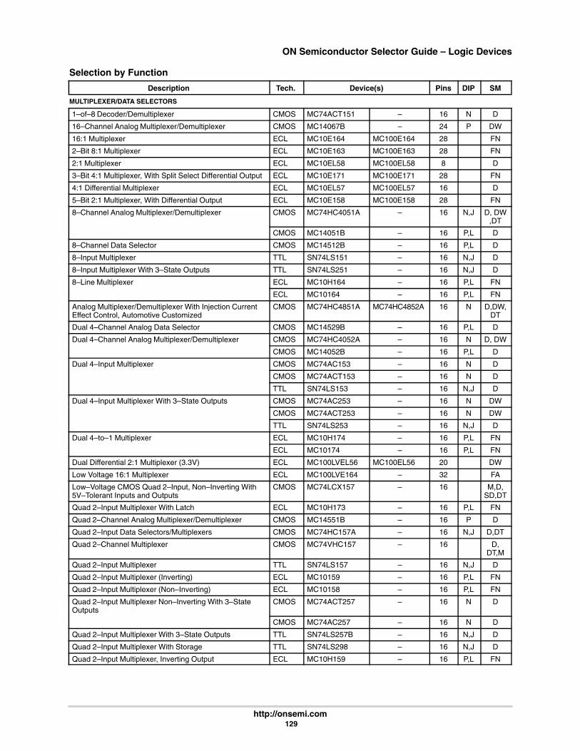
ON Semiconductor Selector Guide – Logic Devices
http://onsemi.com 129
Selection by Function
Description SMDIPPinsDevice(s)Tech.
MULTIPLEXER/DATA SELECTORS
1–of–8 Decoder/Demultiplexer CMOS MC74ACT151 – 16 N D
16–Channel Analog Multiplexer/Demultiplexer CMOS MC14067B – 24 P DW
16:1 Multiplexer ECL MC10E164 MC100E164 28 FN
2–Bit 8:1 Multiplexer ECL MC10E163 MC100E163 28 FN
2:1 Multiplexer ECL MC10EL58 MC100EL58 8 D
3–Bit 4:1 Multiplexer, With Split Select Differential Output ECL MC10E171 MC100E171 28 FN
4:1 Differential Multiplexer ECL MC10EL57 MC100EL57 16 D
5–Bit 2:1 Multiplexer, With Differential Output ECL MC10E158 MC100E158 28 FN
8–Channel Analog Multiplexer/Demultiplexer CMOS MC74HC4051A – 16 N,J D, DW,DT
CMOS MC14051B – 16 P,L D
8–Channel Data Selector CMOS MC14512B – 16 P,L D
8–Input Multiplexer TTL SN74LS151 – 16 N,J D
8–Input Multiplexer With 3–State Outputs TTL SN74LS251 – 16 N,J D
8–Line Multiplexer ECL MC10H164 – 16 P,L FN
ECL MC10164 – 16 P,L FN
Analog Multiplexer/Demultiplexer With Injection CurrentEffect Control, Automotive Customized
CMOS MC74HC4851A MC74HC4852A 16 N D,DW,DT
Dual 4–Channel Analog Data Selector CMOS MC14529B – 16 P,L D
Dual 4–Channel Analog Multiplexer/Demultiplexer CMOS MC74HC4052A – 16 N D, DW
CMOS MC14052B – 16 P,L D
Dual 4–Input Multiplexer CMOS MC74AC153 – 16 N D
CMOS MC74ACT153 – 16 N D
TTL SN74LS153 – 16 N,J D
Dual 4–Input Multiplexer With 3–State Outputs CMOS MC74AC253 – 16 N DW
CMOS MC74ACT253 – 16 N DW
TTL SN74LS253 – 16 N,J D
Dual 4–to–1 Multiplexer ECL MC10H174 – 16 P,L FN
ECL MC10174 – 16 P,L FN
Dual Differential 2:1 Multiplexer (3.3V) ECL MC100LVEL56 MC100EL56 20 DW
Low Voltage 16:1 Multiplexer ECL MC100LVE164 – 32 FA
Low–Voltage CMOS Quad 2–Input, Non–Inverting With5V–Tolerant Inputs and Outputs
CMOS MC74LCX157 – 16 M,D,SD,DT
Quad 2–Input Multiplexer With Latch ECL MC10H173 – 16 P,L FN
Quad 2–Channel Analog Multiplexer/Demultiplexer CMOS MC14551B – 16 P D
Quad 2–Input Data Selectors/Multiplexers CMOS MC74HC157A – 16 N,J D,DT
Quad 2–Channel Multiplexer CMOS MC74VHC157 – 16 D,DT,M
Quad 2–Input Multiplexer TTL SN74LS157 – 16 N,J D
Quad 2–Input Multiplexer (Inverting) ECL MC10159 – 16 P,L FN
Quad 2–Input Multiplexer (Non–Inverting) ECL MC10158 – 16 P,L FN
Quad 2–Input Multiplexer Non–Inverting With 3–StateOutputs
CMOS MC74ACT257 – 16 N D
CMOS MC74AC257 – 16 N D
Quad 2–Input Multiplexer With 3–State Outputs TTL SN74LS257B – 16 N,J D
Quad 2–Input Multiplexer With Storage TTL SN74LS298 – 16 N,J D
Quad 2–Input Multiplexer, Inverting Output ECL MC10H159 – 16 P,L FN

ON Semiconductor Selector Guide – Logic Devices
http://onsemi.com 130
Selection by Function
Description SMDIPPinsDevice(s)Tech.
MULTIPLEXER/DATA SELECTORS
Quad 2–Input Multiplexer, Inverting, With 3–StateOutputs
TTL SN74LS258B – 16 N,J D
Quad 2–Input Multiplexer, Non–Inverting CMOS MC74AC157 – 16 N D
CMOS MC74ACT157 – 16 N D
Quad 2–Input Multiplexer, Non–Inverting Output ECL MC10H158 – 16 P,L FN
Quad 2–Input Multiplexer/Latch ECL MC10173 – 16 P,L FN
Quad 2:1 Mux, Individual–Select ECL MC10E157 MC100E157 28 FN
Quad Analog Switch/Multiplexer CMOS MC14016B – 14 P,L D
CMOS MC14066B – 14 P,L D
Quad Analog Switch/Multiplexer/Demultiplexer CMOS MC74HC4066A – 14 N,J D,DT
Quad Analog Switch/Multiplexer/Demultiplexer WithSeparate Analog/Digital Power Supplies
CMOS MC74HC4316A – 16 N D
Triple 2–Channel Analog Multiplexer/Demultiplexer CMOS MC74HC4053A – 16 N,J D, DW
CMOS MC14053B – 16 P,L D
Triple 2:1 Multiplexer ECL MC100EL59 – 20 DW
Triple 2:1 Multiplexer (3.3V) ECL MC100LVEL59 – 20 DW
Triple Differential 2:1 Multiplexer ECL MC100E457 – 28 FN
ECL MC10E457 – 28 FN
MULTIVIBRATORS
Dual Monostable Multivibrator CMOS MC14528B – 16 P,L D
Dual Monstable Multivibrators With Schmitt Trigger Inputs TTL SN74LS221 – 16 N,J D
Dual Precision Monostable Multivibrator Retriggerable,Resettable)
CMOS MC74HC4538A – 16 N,J D
Dual Precision Monostable Multivibrator CMOS MC14538B – 16 P,L D, DW
Monostable Multivibrator ECL MC10198 – 16 P,L FN
Retriggerable Monostable Multivibrators TTL SN74LS122 – 14 N,J D
TTL SN74LS123 – 14 N,J D
OSCILLATOR/TIMERS
24–Stage Frequency Divider CMOS MC14521B – 16 P,L D
Programmable Oscillator Timer CMOS MC14541B – 14 P,L D
Programmable Timer CMOS MC14536B – 16 P,L DW
PARITY CHECKERS
12–Bit Parity Generator/Checker ECL MC10H160 – 16 P,L FN
12–Bit Parity Generator/Checker, Register–Shiftable, DiffOutput
ECL MC10E160 MC100E160 28 FN
9–Bit Odd/Even Parity Generator/Checker TTL SN74LS280 – 14 N,J D
Error Detection and Correction Circuit ECL MC10E193 MC100E193 28 FN
PHASE–LOCKED LOOP
Phase–Locked Loop CMOS MC14046B – 16 P,L DW
Phase–Locked–Loop With VCO CMOS MC74HC4046A – 16 N D
PROGRAMMABLE DELAY CHIPS
Programmable Delay Chip (Dig 80ps Anal. 1.6 Ps/mv) ECL MC10E196 MC100E196 28 FN
Programmable Delay Chip (Digitally Selectable 20ps Res) ECL MC10E195 MC100E195 28 FN
RECEIVERS
155Mb/s / 622Mb/s Receiver (Demultiplexer) With ClockRecovery
ECL MC10SX1401 – 52 FJ
Differential Receiver ECL MC10EL16 MC100EL16 8 D

ON Semiconductor Selector Guide – Logic Devices
http://onsemi.com 131
Selection by Function
Description SMDIPPinsDevice(s)Tech.
RECEIVERS
Differential Receiver ECL MC100LVEL16 – 8 D
High Speed Triple Line Receiver ECL MC10216 – 16 P,L FN
Low–Voltage Quad Differential Line Receiver ECL MC100LVEL17 MC100EL17 20 DW
Quad Line Receiver ECL MC10H115 – 16 P,L FN
ECL MC10115 – 16 P,L FN
Quint Differential Line Receiver ECL MC10E116 MC100E116 28 FN
ECL MC10E416 MC100E416 28 FN
Triple Line Receiver ECL MC10H116 – 16 P,L D,FN
ECL MC10114 – 16 P,L FN
ECL MC10116 – 16 P,L FN
REGISTERS
8–Bit Serial or Parallel–Input/Serial–Output Shift Register CMOS MC74HC165A – 16 N D,DT
8–Bit Scannable Register ECL MC10E241 MC100E241 28 FN
REGISTER FILES
16 X 4–Bit Register File (RAM) ECL MC10H145 – 16 P,L FN
4 X 4 Register File With 3–State Outputs TTL SN74LS670 – 16 N,J D
SCHMITT TRIGGERS
Hex Inverter Schmitt Trigger CMOS MC74AC14 – 14 N D
CMOS MC74ACT14 – 14 N D
TTL SN74LS14 – 14 N,J D
Hex Schmitt Trigger CMOS MC14106B – 14 P,L D
CMOS MC14584B – 14 P,L D
Hex Schmitt Trigger Inverter CMOS MC74HC14A – 14 N,J D,DT
CMOS MC74VHC14 – 14 D,DT,M
CMOS MC74HCT14A – 14 N,J D
Quad 2–Input NAND Gate With Schmitt Trigger Inputs CMOS MC74HC132A – 14 N,J D
Quad 2–Input NAND Schmitt Trigger CMOS MC74AC132 – 14 N D
CMOS MC74ACT132 – 14 N D
CMOS MC14093B – 14 P,L D
CMOS MC74VHC132 – 14 D,DT,M
Quad 2–Input Schmitt Trigger NAND Gate TTL SN74LS132 – 14 N,J D
SHIFT REGISTERS
1–to–64–Bit Variable Length Shift Register CMOS MC14557B – 16 P,L DW
128–Bit Static Shift Register CMOS MC14562B – 14 P,L
3–Bit Scannable Registered Address Driver, ECL ECL MC10E212 MC100E212 28 FN
4–Bit Bidirectional Universal Shift Register TTL SN74LS194A – 16 N,J D
4–Bit Universal Shift Register ECL MC10H141 – 16 P,L FN
ECL MC10141 – 16 P,L FN
8–Bit Parallel–to–Serial Shift Register TTL SN74LS165 – 16 N,J D
8–Bit Serial or Parallel–Input/Serial–Output Shift RegisterWith 3–State Outputs
CMOS MC74HC589A – 16 N,J D,SDDT
8–Bit Serial–In/Parallel–Out Shift Register TTL SN74LS164 – 14 N,J D
8–Bit Serial–Input/Parallel–Output Shift Register CMOS MC74HC164A – 14 N,J D,DT
8–Bit Serial–Input/Serial or Parallel–Output Shift RegisterWith Latched 3–State Outputs
CMOS MC74HC595A – 16 N,J D,DT
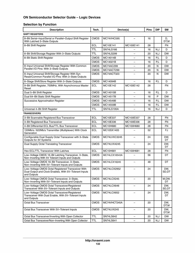
ON Semiconductor Selector Guide – Logic Devices
http://onsemi.com 132
Selection by Function
Description SMDIPPinsDevice(s)Tech.
SHIFT REGISTERS
8–Bit Serial–Input/Serial or Parallel–Output Shift RegisterWith Latched 3–State Outputs
CMOS MC74VHC595 – 16 D,DT,M
8–Bit Shift Register ECL MC10E141 MC100E141 28 FN
TTL SN74LS166 – 16 N,J D
8–Bit Shift/Storage Register With 3–State Outputs TTL SN74LS299 – 20 N,J DW
8–Bit Static Shift Register CMOS MC14014B – 16 P,L D
CMOS MC14021B – 16 P,L D
8–Input Universal Shift/Storage Register With CommonP ll l I/O Pi With 3 St t O t t
CMOS MC74AC299 – 20 N DWParallel I/O Pins: With 3–State Outputs CMOS MC74ACT299 – 20 N DW
8–Input Universal Shift/Storage Register With Syn CMOS MC74ACT323 – 20 N DWg g yReset/Common Parallel I/O Pins: With 3–State Outputs
8–Stage Shift/Store Register With 3–State Outputs CMOS MC14094B – 16 P,L D
9–Bit Shift Register, 700MHz, With Asynchronous MasterReset
ECL MC10E142 MC100E142 28 FN
Dual 5–Bit Shift Register CMOS MC14015B – 16 P,L D
Dual 64–Bit Static Shift Register CMOS MC14517B – 16 P DW
Successive Approximation Register CMOS MC14549B – 16 P,L DW
CMOS MC14559B – 16 P,L DW
Universal 4–Bit Shift Register TTL SN74LS195A – 16 N,J D
TRANSCEIVERS
3–Bit Scannable Registered Bus Transceiver ECL MC10E337 MC100E337 28 FN
3–Bit Registered Bus Transceiver ECL MC10E336 MC100E336 28 FN
4–Bit Differential ECL Bus/TTL Bus Transceiver ECL MC10H680 MC100H680 28 FN
155Mb/s / 622Mb/s Transmitter (Multiplexer) With ClockGeneration
ECL MC10SX1405 – 52 FJ
Configurable Dual Supply Octal Transceiver with 3–StateOutputs for 3V Systems
CMOS MC74LVXC3245 – 24 DW,DT
Dual Supply Octal Translating Transceiver CMOS MC74LVX4245 – 24 DW,DT
Hex ECL/TTL Transceiver With Latches ECL MC10H681 MC100H681 28 FN
Low–Voltage CMOS 16–Bit Latching Transceiver, 3–State,Non–Inverting With 5V Tolerant Inputs and Outputs
CMOS MC74LCX16543A – 56 DT
Low–Voltage CMOS 16–Bit Transceiver, 3–State,Non–Inverting With 5V–Tolerant Inputs and Outputs
CMOS MC74LCX16245 – 48 DT
Low–Voltage CMOS Octal Registered Transceiver WithDual Output and Clock Enables, With 5V–Tolerant Inputsand Outputs
CMOS MC74LCX2952 – 24 DW,SD,DT
Low–Voltage CMOS Octal Transceiver, 3–State,Non–Inverting With 5V–Tolerant Inputs and Outputs
CMOS MC74LCX245 – 20 M,DW,DT
Low–Voltage CMOS Octal Transceiver/RegisteredTransceiver With 5V–Tolerant Inputs and Outputs
CMOS MC74LCX646 – 24 DW,SD,DT
Low–Voltage CMOS Octal Transceiver/RegisteredTransceiver With Dual Enable, With 5V–Tolerant Inputsand Outputs
CMOS MC74LCX652 – 24 DW,DT
Octal Bus Transceiver CMOS MC74VHCT245A – 20 DW,DT,M
Octal Bus Transceiver With 5V–Tolerant Inputs CMOS MC74LVX245 – 20 DW,DT,M
Octal Bus Transceiver/Inverting With Open Collector TTL SN74LS642 – 20 N,J DW
Octal Bus Transceiver/Non–Inverting With Open Collector TTL SN74LS641 – 20 N,J DW

ON Semiconductor Selector Guide – Logic Devices
http://onsemi.com 133
Selection by Function
Description SMDIPPinsDevice(s)Tech.
TRANSLATORS
9–Bit ECL/TTL Translator ECL MC10H601 MC100H601 28 FN
9–Bit Latch ECL/TTL Translator ECL MC10H603 MC100H603 28 FN
9–Bit Latch TTL/ECL Translator ECL MC10H602 MC100H602 28 FN
9–Bit TTL/ECL Translator ECL MC10H600 MC100H600 28 FN
1:2 Fanout Differential PECL to TTL Translator ECL MC10ELT26 MC100ELT26 8 D
Differential ECL/TTL Translator ECL MC10ELT25 MC100ELT25 8 D
Differential PECL/TTL Translator ECL MC10ELT21 MC100ELT21 8 D
Dual Differential PECL/TTL Translator ECL MC100ELT23 – 8 D
Dual LVTTL/LVCMOS to Differential PECL Translator ECL MC100LVELT22 – 8 D
Dual TTL/Differential PECL Translator ECL MC10ELT22 MC100ELT22 8 D
ECL/TTL Translator (Single P.S. @+ 5.0V) ECL MC10H350 – 16 P,L FN
Hex TTL OR CMOS/CMOS Hex Level Shifter CMOS MC14504B – 16 P,L D
Quad CMOS/ECL Translator (Single P.S. @+ 5.0V) ECL MC10H352 – 20 P,L FN
Quad MECL/TTL Translator ECL MC10H125 – 16 P,L FN
ECL MC10125 – 16 P,L FN
Quad TTL/ECL Translator (ECL Strobe) ECL MC10H424 – 16 P,L FN
Quad TTL/MECL Translator ECL MC10124 – 16 P,L FN
Quad TTL/MECL Translator, With TTL Strobe Input ECL MC10H124 – 16 P,L FN
Quad TTL/NMOS–to–PECL Translator (Single P.S. @+5.0V)
ECL MC10H351 – 20 P,L FN
Registered Hex ECL/TTL Translator ECL MC10H605 MC100H605 28 FN
Registered Hex PECL/TTL Translator ECL MC10H607 MC100H607 28 FN
Registered Hex TTL/ECL Translator ECL MC10H604 MC100H604 28 FN
Registered Hex TTL/PECL Translator ECL MC10H606 MC100H606 28 FN
Triple ECL to PECL Translator ECL MC100LVEL90 MC100EL90 20 DW
Triple PECL to LVPECL Translator ECL MC100LVEL92 – 20 DW
Triple PECL to ECL Translator ECL MC100LVEL91 MC100EL91 20 DW
TTL/Differential ECL Translator ECL MC10ELT24 MC100ELT24 8 D
TTL/Differential PECL Translator ECL MC10ELT20 MC100ELT20 8 D
TTL to Differential PECL/Differential PECL to TTL Translator ECL MC10ELT28 MC100ELT28 8 D
VCO
Phase–Locked–Loop With VCO CMOS MC74HC4046A – 16 N D
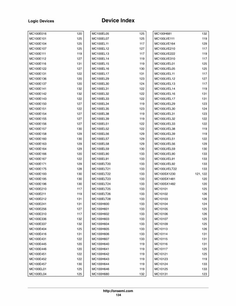
Device IndexLogic Devices
http://onsemi.com 134
MC100E016 120
MC100E101 125
MC100E104 125
MC100E107 125
MC100E111 119
MC100E112 127
MC100E116 131
MC100E122 127
MC100E131 122
MC100E136 120
MC100E137 120
MC100E141 132
MC100E142 132
MC100E143 122
MC100E150 127
MC100E151 122
MC100E154 127
MC100E155 127
MC100E156 127
MC100E157 130
MC100E158 129
MC100E160 130
MC100E163 129
MC100E164 129
MC100E166 120
MC100E167 122
MC100E171 129
MC100E175 128
MC100E193 130
MC100E195 130
MC100E196 130
MC100E210 117
MC100E211 119
MC100E212 131
MC100E241 131
MC100E256 127
MC100E310 117
MC100E336 132
MC100E337 132
MC100E404 125
MC100E416 131
MC100E431 122
MC100E445 120
MC100E446 120
MC100E451 122
MC100E452 122
MC100E457 130
MC100EL01 125
MC100EL04 125
MC100EL05 125
MC100EL07 125
MC100EL11 117
MC100EL12 127
MC100EL13 117
MC100EL14 119
MC100EL15 119
MC100EL16 130
MC100EL17 131
MC100EL29 123
MC100EL30 124
MC100EL31 122
MC100EL32 122
MC100EL33 122
MC100EL34 119
MC100EL35 123
MC100EL38 119
MC100EL39 119
MC100EL51 122
MC100EL52 122
MC100EL56 129
MC100EL57 129
MC100EL58 129
MC100EL59 130
MC100EL90 133
MC100EL91 133
MC100ELT20 133
MC100ELT21 133
MC100ELT22 133
MC100ELT23 133
MC100ELT24 133
MC100ELT25 133
MC100ELT26 133
MC100ELT28 133
MC100H600 133
MC100H601 133
MC100H602 133
MC100H603 133
MC100H604 133
MC100H605 133
MC100H606 133
MC100H607 133
MC100H640 119
MC100H641 119
MC100H642 119
MC100H643 119
MC100H644 119
MC100H646 119
MC100H680 132
MC100H681 132
MC100LVE111 119
MC100LVE164 129
MC100LVE210 117
MC100LVE222 119
MC100LVE310 117
MC100LVEL01 125
MC100LVEL05 125
MC100LVEL11 117
MC100LVEL12 127
MC100LVEL13 117
MC100LVEL14 119
MC100LVEL16 131
MC100LVEL17 131
MC100LVEL29 123
MC100LVEL30 124
MC100LVEL31 123
MC100LVEL32 122
MC100LVEL33 122
MC100LVEL38 119
MC100LVEL39 119
MC100LVEL51 122
MC100LVEL56 129
MC100LVEL59 130
MC100LVEL90 133
MC100LVEL91 133
MC100LVEL92 133
MC100LVELT22 133
MC100SX1230 121, 122
MC100SX1481 120
MC100SX1482 120
MC10101 125
MC10102 126
MC10103 126
MC10104 124
MC10105 125
MC10106 126
MC10107 125
MC10109 125
MC10113 126
MC10114 131
MC10115 131
MC10116 131
MC10117 125
MC10121 125
MC10123 119
MC10124 133
MC10125 133
MC10131 123

Device Index Logic Devices
http://onsemi.com 135
MC10135 123
MC10136 121
MC10138 120
MC10141 131
MC10153 128
MC10158 129
MC10159 129
MC10161 121
MC10162 121
MC10164 129
MC10171 121
MC10173 130
MC10174 129
MC10175 128
MC10176 123
MC10178 120
MC10186 123
MC10188 127
MC10189 127
MC10192 119
MC10195 127
MC10197 124
MC10198 130
MC10216 131
MC10231 123
MC10E016 120
MC10E101 125
MC10E104 125
MC10E107 125
MC10E111 119
MC10E112 127
MC10E116 131
MC10E122 127
MC10E131 122
MC10E136 120
MC10E137 120
MC10E141 132
MC10E142 132
MC10E143 122
MC10E150 127
MC10E151 122
MC10E154 127
MC10E155 127
MC10E156 127
MC10E157 130
MC10E158 129
MC10E160 130
MC10E163 129
MC10E164 129
MC10E1651 120
MC10E1652 120
MC10E166 120
MC10E167 122
MC10E171 129
MC10E175 128
MC10E193 130
MC10E195 130
MC10E196 130
MC10E197 128
MC10E211 119
MC10E212 131
MC10E241 131
MC10E256 127
MC10E336 132
MC10E337 132
MC10E404 125
MC10E411 119
MC10E416 131
MC10E431 122
MC10E445 120
MC10E446 120
MC10E451 122
MC10E452 122
MC10E457 130
MC10EL01 125
MC10EL04 125
MC10EL05 125
MC10EL07 125
MC10EL11 117
MC10EL12 127
MC10EL15 119
MC10EL16 130
MC10EL31 122
MC10EL32 122
MC10EL33 122
MC10EL34 119
MC10EL35 123
MC10EL51 122
MC10EL52 122
MC10EL57 129
MC10EL58 129
MC10EL89 122
MC10ELT20 133
MC10ELT21 133
MC10ELT22 133
MC10ELT24 133
MC10ELT25 133
MC10ELT26 133
MC10ELT28 133
MC10H016 120
MC10H100 126
MC10H101 125
MC10H102 126
MC10H103 126
MC10H104 124
MC10H105 125
MC10H106 126
MC10H107 125
MC10H109 125
MC10H113 126
MC10H115 131
MC10H116 131
MC10H117 125
MC10H121 125
MC10H123 119
MC10H124 133
MC10H125 133
MC10H130 128
MC10H131 123
MC10H135 123
MC10H136 121
MC10H141 131
MC10H145 131
MC10H158 130
MC10H159 129
MC10H160 130
MC10H161 121
MC10H162 121
MC10H164 129
MC10H165 122
MC10H166 120
MC10H171 121
MC10H172 121
MC10H173 129
MC10H174 129
MC10H175 128
MC10H176 123
MC10H179 117
MC10H180 117
MC10H181 117
MC10H186 123
MC10H188 127
MC10H189 127
MC10H209 125
MC10H210 126
MC10H211 126
MC10H330 119
MC10H332 118
MC10H334 119
MC10H350 133

Device IndexLogic Devices
http://onsemi.com 136
MC10H351 133
MC10H352 133
MC10H424 133
MC10H600 133
MC10H601 133
MC10H602 133
MC10H603 133
MC10H604 133
MC10H605 133
MC10H606 133
MC10H607 133
MC10H640 119
MC10H641 119
MC10H642 119
MC10H643 119
MC10H644 119
MC10H645 119
MC10H646 119
MC10H680 132
MC10H681 132
MC10SX1125 117
MC10SX1130 119, 122
MC10SX1189 119
MC10SX1401 130
MC10SX1405 132
MC14001B 126
MC14001UB 126
MC14007UB 127
MC14008B 117
MC14011B 125
MC14011UB 125
MC14012B 124
MC14013B 122
MC14014B 132
MC14015B 132
MC14016B 130
MC14017B 120
MC14018B 120
MC14020B 120
MC14021B 132
MC14022B 120
MC14023B 125
MC14024B 120
MC14025B 126
MC14027B 123
MC14028B 121
MC14029B 120
MC14040B 120
MC14042B 128
MC14043B 128
MC14044B 128
MC14046B 130
MC14049B 127
MC14049UB 127
MC14050B 127
MC14051B 129
MC14052B 129
MC14053B 130
MC14060B 120
MC14066B 130
MC14067B 129
MC14069UB 127
MC14070B 126
MC14071B 126
MC14073B 125
MC14076B 124
MC14077B 126
MC14081B 124
MC14082B 124
MC14093B 131
MC14094B 132
MC14099B 127
MC14106B 131
MC14174B 123
MC14175B 124
MC14490 117
MC14503B 118
MC14504B 133
MC14511B 121
MC14512B 129
MC14513B 122
MC14514B 121
MC14515B 121
MC14516B 120
MC14517B 132
MC14518B 120
MC14520B 120
MC14521B 130
MC14526B 120
MC14528B 130
MC14529B 129
MC14532B 122
MC14536B 130
MC14538B 130
MC14541B 130
MC14543B 122
MC14549B 132
MC14551B 129
MC14553B 120
MC14555B 121
MC14556B 121
MC14557B 131
MC14559B 132
MC14562B 131
MC14569B 120
MC14572UB 125
MC14584B 131
MC14585B 119
MC14598B 128
MC68194 119
MC74AC00 124
MC74AC02 126
MC74AC04 127
MC74AC05 127
MC74AC08 124
MC74AC10 125
MC74AC109 123
MC74AC11 125
MC74AC125 119
MC74AC132 131
MC74AC138 121
MC74AC139 121
MC74AC14 131
MC74AC151 128
MC74AC153 129
MC74AC157 130
MC74AC161 121
MC74AC163 121
MC74AC174 123
MC74AC175 124
MC74AC20 124
MC74AC240 118
MC74AC244 118
MC74AC245 118
MC74AC253 129
MC74AC257 129
MC74AC259 127
MC74AC273 123
MC74AC299 132
MC74AC32 126
MC74AC373 128
MC74AC374 123
MC74AC377 123
MC74AC540 118
MC74AC541 118
MC74AC573 128
MC74AC574 124
MC74AC646 118
MC74AC652 118
MC74AC74 122
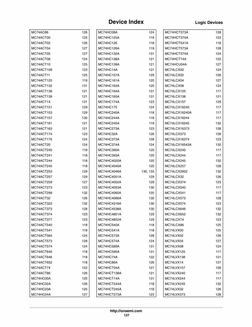
Device Index Logic Devices
http://onsemi.com 137
MC74AC86 126
MC74ACT00 125
MC74ACT02 126
MC74ACT04 127
MC74ACT05 127
MC74ACT08 124
MC74ACT10 125
MC74ACT109 123
MC74ACT11 125
MC74ACT125 119
MC74ACT132 131
MC74ACT138 121
MC74ACT139 121
MC74ACT14 131
MC74ACT151 129
MC74ACT153 129
MC74ACT157 130
MC74ACT161 121
MC74ACT163 121
MC74ACT174 123
MC74ACT175 124
MC74ACT20 124
MC74ACT240 118
MC74ACT241 118
MC74ACT244 118
MC74ACT245 118
MC74ACT253 129
MC74ACT257 129
MC74ACT259 127
MC74ACT273 123
MC74ACT299 132
MC74ACT32 126
MC74ACT323 132
MC74ACT373 128
MC74ACT374 123
MC74ACT377 123
MC74ACT540 118
MC74ACT541 118
MC74ACT564 124
MC74ACT573 128
MC74ACT574 124
MC74ACT640 118
MC74ACT646 118
MC74ACT652 118
MC74ACT74 122
MC74ACT86 126
MC74HC00A 125
MC74HC02A 126
MC74HC03A 125
MC74HC04A 127
MC74HC08A 124
MC74HC125A 119
MC74HC126 118
MC74HC126A 119
MC74HC132A 131
MC74HC138A 121
MC74HC139A 121
MC74HC14A 131
MC74HC157A 129
MC74HC161A 120
MC74HC163A 120
MC74HC164A 131
MC74HC165A 131
MC74HC174A 123
MC74HC175 124
MC74HC240A 118
MC74HC244A 118
MC74HC245A 119
MC74HC273A 123
MC74HC32A 126
MC74HC373A 128
MC74HC374A 124
MC74HC390A 120
MC74HC393A 120
MC74HC4020A 120
MC74HC4040A 120
MC74HC4046A 130, 133
MC74HC4051A 129
MC74HC4052A 129
MC74HC4053A 130
MC74HC4060A 120
MC74HC4066A 130
MC74HC4316A 130
MC74HC4538A 130
MC74HC4851A 129
MC74HC4852A 129
MC74HC540A 118
MC74HC541A 118
MC74HC573A 128
MC74HC574A 124
MC74HC589A 131
MC74HC595A 131
MC74HC74A 122
MC74HC86A 126
MC74HCT04A 127
MC74HCT138A 121
MC74HCT14A 131
MC74HCT244A 118
MC74HCT245A 118
MC74HCT273A 123
MC74HCT373A 128
MC74HCT374A 123
MC74HCT541A 118
MC74HCT573A 128
MC74HCT574A 124
MC74HCT74A 122
MC74HCU04A 127
MC74LCX00 124
MC74LCX02 126
MC74LCX04 127
MC74LCX08 124
MC74LCX125 117
MC74LCX138 121
MC74LCX157 129
MC74LCX16240 117
MC74LCX16240A 117
MC74LCX16244 117
MC74LCX16245 132
MC74LCX16373 128
MC74LCX373 128
MC74LCX16374 123
MC74LCX16543A 132
MC74LCX240 117
MC74LCX244 117
MC74LCX245 132
MC74LCX257 128
MC74LCX2952 132
MC74LCX32 126
MC74LCX374 123
MC74LCX540 117
MC74LCX541 117
MC74LCX573 128
MC74LCX574 123
MC74LCX646 132
MC74LCX652 132
MC74LCX74 123
MC74LCX86 125
MC74LVX00 125
MC74LVX02 126
MC74LVX04 127
MC74LVX08 124
MC74LVX125 117
MC74LVX138 121
MC74LVX14 127
MC74LVX157 128
MC74LVX240 117
MC74LVX244 117
MC74LVX245 132
MC74LVX32 126
MC74LVX373 128
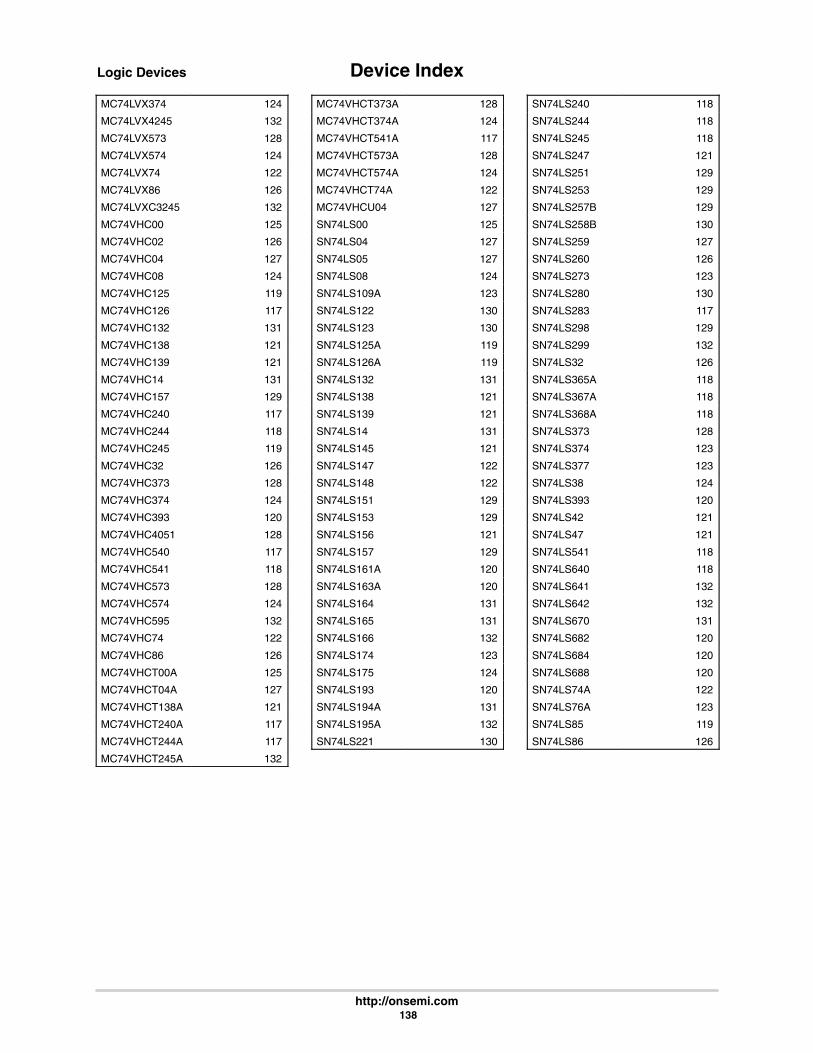
Device IndexLogic Devices
http://onsemi.com 138
MC74LVX374 124
MC74LVX4245 132
MC74LVX573 128
MC74LVX574 124
MC74LVX74 122
MC74LVX86 126
MC74LVXC3245 132
MC74VHC00 125
MC74VHC02 126
MC74VHC04 127
MC74VHC08 124
MC74VHC125 119
MC74VHC126 117
MC74VHC132 131
MC74VHC138 121
MC74VHC139 121
MC74VHC14 131
MC74VHC157 129
MC74VHC240 117
MC74VHC244 118
MC74VHC245 119
MC74VHC32 126
MC74VHC373 128
MC74VHC374 124
MC74VHC393 120
MC74VHC4051 128
MC74VHC540 117
MC74VHC541 118
MC74VHC573 128
MC74VHC574 124
MC74VHC595 132
MC74VHC74 122
MC74VHC86 126
MC74VHCT00A 125
MC74VHCT04A 127
MC74VHCT138A 121
MC74VHCT240A 117
MC74VHCT244A 117
MC74VHCT245A 132
MC74VHCT373A 128
MC74VHCT374A 124
MC74VHCT541A 117
MC74VHCT573A 128
MC74VHCT574A 124
MC74VHCT74A 122
MC74VHCU04 127
SN74LS00 125
SN74LS04 127
SN74LS05 127
SN74LS08 124
SN74LS109A 123
SN74LS122 130
SN74LS123 130
SN74LS125A 119
SN74LS126A 119
SN74LS132 131
SN74LS138 121
SN74LS139 121
SN74LS14 131
SN74LS145 121
SN74LS147 122
SN74LS148 122
SN74LS151 129
SN74LS153 129
SN74LS156 121
SN74LS157 129
SN74LS161A 120
SN74LS163A 120
SN74LS164 131
SN74LS165 131
SN74LS166 132
SN74LS174 123
SN74LS175 124
SN74LS193 120
SN74LS194A 131
SN74LS195A 132
SN74LS221 130
SN74LS240 118
SN74LS244 118
SN74LS245 118
SN74LS247 121
SN74LS251 129
SN74LS253 129
SN74LS257B 129
SN74LS258B 130
SN74LS259 127
SN74LS260 126
SN74LS273 123
SN74LS280 130
SN74LS283 117
SN74LS298 129
SN74LS299 132
SN74LS32 126
SN74LS365A 118
SN74LS367A 118
SN74LS368A 118
SN74LS373 128
SN74LS374 123
SN74LS377 123
SN74LS38 124
SN74LS393 120
SN74LS42 121
SN74LS47 121
SN74LS541 118
SN74LS640 118
SN74LS641 132
SN74LS642 132
SN74LS670 131
SN74LS682 120
SN74LS684 120
SN74LS688 120
SN74LS74A 122
SN74LS76A 123
SN74LS85 119
SN74LS86 126
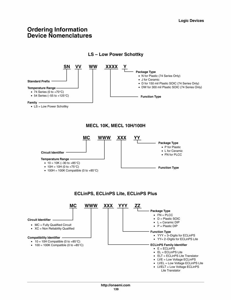
Logic Devices
http://onsemi.com 139
Ordering InformationDevice Nomenclatures
LS – Low Power Schottky
Standard Prefix
Temperature Range• 74 Series (0 to +70°C)• 54 Series (–55 to +125°C)
Family• LS = Low Power Schottky
Package Type• N for Plastic (74 Series Only)• J for Ceramic• D for 150 mil Plastic SOIC (74 Series Only)• DW for 300 mil Plastic SOIC (74 Series Only)
Function Type
SN VV WW XXXX Y
MECL 10K, MECL 10H/100H
Circuit Identifier
Temperature Range• 10 = 10K (–30 to +85°C)• 10H = 10H (0 to +75°C)• 100H = 100K Compatible (0 to +85°C)
Package Type• P for Plastic• L for Ceramic• FN for PLCC
Function Type
MC WWW XXX YY
ECLinPS, ECLinPS Lite, ECLinPS Plus
XXX
Circuit Identifier
Compatibility Identifier• 10 = 10H Compatible (0 to +85°C)• 100 = 100K Compatible (0 to +85°C)
Package Type• FN = PLCC• D = Plastic SOIC• L = Ceramic DIP• P = Plastic DIP
Function Type
MC WWW YYY ZZ
ECLinPS Family Identifier
• YYY = 3–Digits for ECLinPS• YY= 2–Digits for ECLinPS Lite
• E = ECLinPS• EL = ECLinPS Lite• ELT = ECLinPS Lite Translator• LVE = Low Voltage ECLinPS• LVEL = Low Voltage ECLinPS Lite• LVELT = Low Voltage ECLinPS
Lite Translator
• MC = Fully Qualified Circuit• XC = Non Reliability Qualified
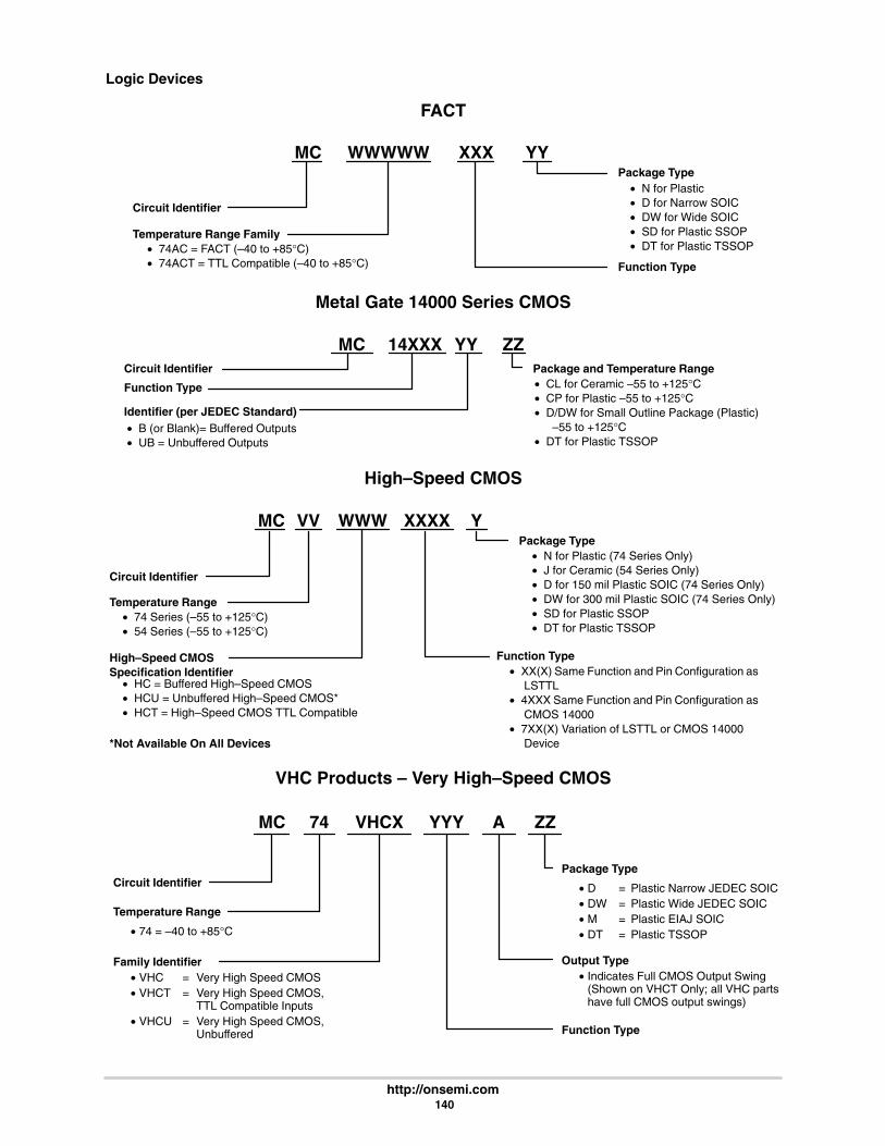
Logic Devices
http://onsemi.com 140
FACT
Circuit Identifier
Temperature Range Family• 74AC = FACT (–40 to +85°C)• 74ACT = TTL Compatible (–40 to +85°C)
Package Type• N for Plastic• D for Narrow SOIC• DW for Wide SOIC• SD for Plastic SSOP• DT for Plastic TSSOP
Function Type
MC WWWWW XXX YY
Metal Gate 14000 Series CMOS
MC 14XXX ZZYYCircuit Identifier Package and Temperature Range
• CL for Ceramic –55 to +125°C• CP for Plastic –55 to +125°C• D/DW for Small Outline Package (Plastic)
–55 to +125°C• DT for Plastic TSSOP
Function Type
Identifier (per JEDEC Standard)• B (or Blank)= Buffered Outputs• UB = Unbuffered Outputs
High–Speed CMOS
Circuit Identifier
Temperature Range• 74 Series (–55 to +125°C)• 54 Series (–55 to +125°C)
High–Speed CMOSSpecification Identifier
• HC = Buffered High–Speed CMOS• HCU = Unbuffered High–Speed CMOS*• HCT = High–Speed CMOS TTL Compatible
*Not Available On All Devices
Package Type• N for Plastic (74 Series Only)• J for Ceramic (54 Series Only)• D for 150 mil Plastic SOIC (74 Series Only)• DW for 300 mil Plastic SOIC (74 Series Only)• SD for Plastic SSOP• DT for Plastic TSSOP
Function Type• XX(X) Same Function and Pin Configuration as
LSTTL• 4XXX Same Function and Pin Configuration as
CMOS 14000• 7XX(X) Variation of LSTTL or CMOS 14000
Device
MC VV WWW XXXX Y
VHC Products – Very High–Speed CMOS
MC 74 VHCX YYY ZZ
Circuit Identifier
Temperature Range
• 74 = –40 to +85°C
Family Identifier• VHC = Very High Speed CMOS• VHCT = Very High Speed CMOS,
TTL Compatible Inputs• VHCU = Very High Speed CMOS,
Unbuffered
Package Type
• D = Plastic Narrow JEDEC SOIC• DW = Plastic Wide JEDEC SOIC• M = Plastic EIAJ SOIC• DT = Plastic TSSOP
Function Type
A
Output Type• Indicates Full CMOS Output Swing
(Shown on VHCT Only; all VHC partshave full CMOS output swings)

Logic Devices
http://onsemi.com 141
LCX Products – Low Voltage CMOS
Circuit Identifier
Temperature Range• 74 = –40 to +85°C
Family Identifier• LCX = 5V–Tolerant Low–Voltage CMOS
Package Type• D for Plastic Narrow JEDEC SOIC• DW for Plastic Wide JEDEC SOIC• M for Plastic EIAJ SOIC• SD for Plastic SSOP• DT for Plastic TSSOP
Function Type
MC 74 LCX YYYYY ZZ
LVX Products – Low Voltage CMOS
MC 74 LVX ZZ
Circuit Identifier
Temperature Range
• 74 = –40 to +85°C
Family Identifier
Package Type
• D = Plastic Narrow JEDEC SOIC• DW = Plastic Wide JEDEC SOIC• M = Plastic EIAJ SOIC• DT = Plastic TSSOP
Configurable• Blank = Non–Configurable• C = Configurable
C
Function Type
YYY
VCX Products – Very Low–Voltage CMOS
Circuit Identifier
Temperature Range• 74 = –40 to +85°C
Family Identifier
Package Type• D for Plastic Narrow JEDEC SOIC• DW for Plastic Wide JEDEC SOIC• M for Plastic EIAJ SOIC• SD for Plastic SSOP• DT for Plastic TSSOP
Function Type
MC 74 VCX YYYYY ZZ
Other Logic Circuits
• N for Plastic• D for Narrow SOIC• FN for PLCC• FJ for CLCC
Circuit Identifier
Function Type
Package Type
Option Type
MC/MCCS WWWWWW X YY ZZ
Option Suffix Indicator
• MC = Standard Circuit Identifier• MCCS = Circuit Chip–Set Identifier
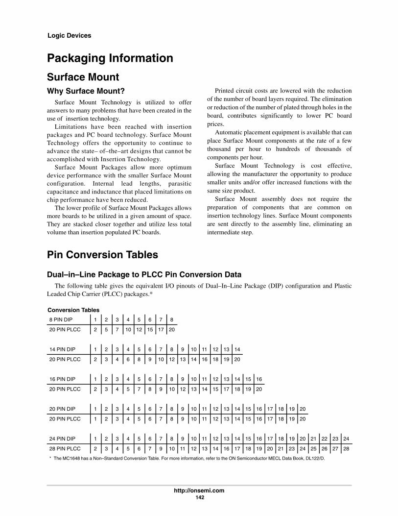
Logic Devices
http://onsemi.com 142
Packaging Information
Surface MountWhy Surface Mount?
Surface Mount Technology is utilized to offeranswers to many problems that have been created in theuse of insertion technology.
Limitations have been reached with insertionpackages and PC board technology. Surface MountTechnology offers the opportunity to continue toadvance the state– of–the–art designs that cannot beaccomplished with Insertion Technology.
Surface Mount Packages allow more optimumdevice performance with the smaller Surface Mountconfiguration. Internal lead lengths, parasiticcapacitance and inductance that placed limitations onchip performance have been reduced.
The lower profile of Surface Mount Packages allowsmore boards to be utilized in a given amount of space.They are stacked closer together and utilize less totalvolume than insertion populated PC boards.
Printed circuit costs are lowered with the reductionof the number of board layers required. The eliminationor reduction of the number of plated through holes in theboard, contributes significantly to lower PC boardprices.
Automatic placement equipment is available that canplace Surface Mount components at the rate of a fewthousand per hour to hundreds of thousands ofcomponents per hour.
Surface Mount Technology is cost effective,allowing the manufacturer the opportunity to producesmaller units and/or offer increased functions with thesame size product.
Surface Mount assembly does not require thepreparation of components that are common oninsertion technology lines. Surface Mount componentsare sent directly to the assembly line, eliminating anintermediate step.
Pin Conversion Tables
Dual–in–Line Package to PLCC Pin Conversion DataThe following table gives the equivalent I/O pinouts of Dual–In–Line Package (DIP) configuration and Plastic
Leaded Chip Carrier (PLCC) packages.*
Conversion Tables
8 PIN DIP 1 2 3 4 5 6 7 8
20 PIN PLCC 2 5 7 10 12 15 17 20
14 PIN DIP 1 2 3 4 5 6 7 8 9 10 11 12 13 14
20 PIN PLCC 2 3 4 6 8 9 10 12 13 14 16 18 19 20
16 PIN DIP 1 2 3 4 5 6 7 8 9 10 11 12 13 14 15 16
20 PIN PLCC 2 3 4 5 7 8 9 10 12 13 14 15 17 18 19 20
20 PIN DIP 1 2 3 4 5 6 7 8 9 10 11 12 13 14 15 16 17 18 19 20
20 PIN PLCC 1 2 3 4 5 6 7 8 9 10 11 12 13 14 15 16 17 18 19 20
24 PIN DIP 1 2 3 4 5 6 7 8 9 10 11 12 13 14 15 16 17 18 19 20 21 22 23 24
28 PIN PLCC 2 3 4 5 6 7 9 10 11 12 13 14 16 17 18 19 20 21 23 24 25 26 27 28
* The MC1648 has a Non–Standard Conversion Table. For more information, refer to the ON Semiconductor MECL Data Book, DL122/D.
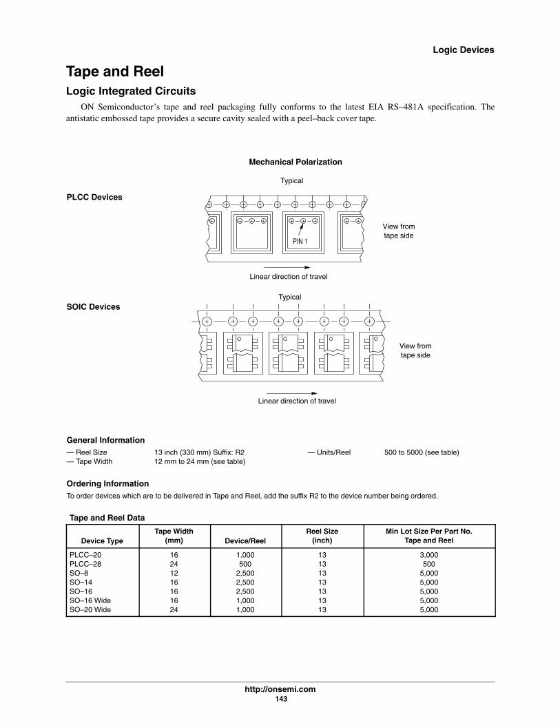
Logic Devices
http://onsemi.com 143
Tape and ReelLogic Integrated Circuits
ON Semiconductor’s tape and reel packaging fully conforms to the latest EIA RS–481A specification. Theantistatic embossed tape provides a secure cavity sealed with a peel–back cover tape.
Mechanical Polarization
PLCC Devices
General Information— Reel Size 13 inch (330 mm) Suffix: R2 — Units/Reel 500 to 5000 (see table)— Tape Width 12 mm to 24 mm (see table)
Ordering InformationTo order devices which are to be delivered in Tape and Reel, add the suffix R2 to the device number being ordered.
SOIC Devices
Linear direction of travel
PIN 1
View fromtape side
Typical
Linear direction of travel
View fromtape side
Typical
Tape and Reel Data
Device TypeTape Width
(mm) Device/ReelReel Size
(inch)Min Lot Size Per Part No.
Tape and Reel
PLCC–20PLCC–28SO–8SO–14SO–16SO–16 WideSO–20 Wide
16241216161624
1,000500
2,5002,5002,5001,0001,000
13131313131313
3,000500
5,0005,0005,0005,0005,000

Logic Devices
http://onsemi.com 144
ON Semiconductor Selector Guide – Discrete Devices
http://onsemi.com 145
Small Signal Transistors,FETs and Diodes
In Brief . . .
PageBipolar Transistors 146. . . . . . . . . . . . . . . . . . . . . . . . . . . .
Plastic–Encapsulated Transistors 146. . . . . . . . . . . . Plastic–Encapsulated SurfaceMount Transistors 149. . . . . . . . . . . . . . . . . . . . . . . . .
Field–Effect Transistors 155. . . . . . . . . . . . . . . . . . . . . . . JFETs 155. . . . . . . . . . . . . . . . . . . . . . . . . . . . . . . . . . . . MOSFETs 156. . . . . . . . . . . . . . . . . . . . . . . . . . . . . . . .
Tuning and Switching Diodes 157. . . . . . . . . . . . . . . . . . Tuning Diodes — Abrupt Junction 157. . . . . . . . . . . . Tuning Diodes — Hyper–Abrupt Junction 157. . . . . Schottky Diodes 158. . . . . . . . . . . . . . . . . . . . . . . . . . . Switching Diodes 159. . . . . . . . . . . . . . . . . . . . . . . . . .
This section highlights semiconductors that are themost popular and have a history of high usage for mostapplications.
It covers a wide range of Small Signal plasticsemiconductors.
A large selection of encapsulated plastic transistors,FETs and diodes are available for surface mount andinsertion assembly technology. Plastic packages includeTO–92 (TO–226AA), 1 Watt TO–92 (TO–226AE),SOT–23, SC–59, SC–70/SOT–323 and SOT–223.
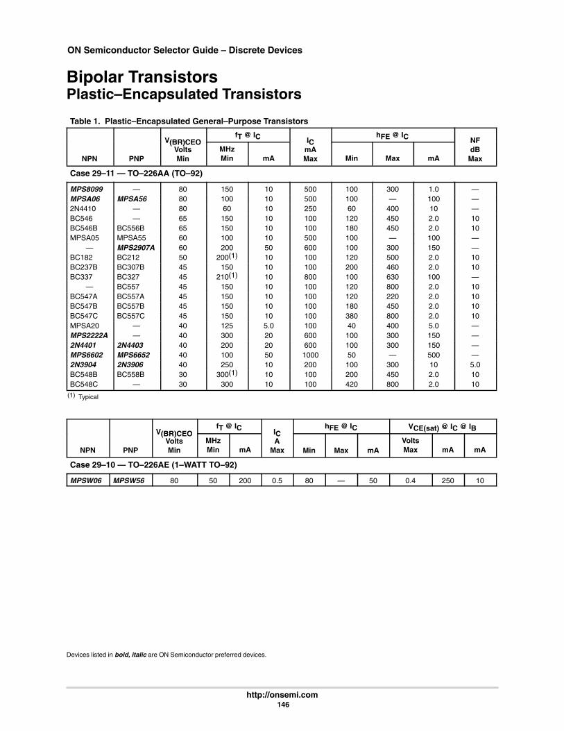
ON Semiconductor Selector Guide – Discrete Devices
http://onsemi.com 146
Bipolar TransistorsPlastic–Encapsulated Transistors
Table 1. Plastic–Encapsulated General–Purpose Transistors
V(BR)CEOfT @ IC IC
hFE @ IC NF
NPN PNP
V(BR)CEOVoltsMin
MHzMin mA
ICmAMax Min Max mA
NFdB
Max
Case 29–11 — TO–226AA (TO–92)
MPS8099 — 80 150 10 500 100 300 1.0 —MPSA06 MPSA56 80 100 10 500 100 — 100 —2N4410 — 80 60 10 250 60 400 10 —BC546 — 65 150 10 100 120 450 2.0 10BC546B BC556B 65 150 10 100 180 450 2.0 10MPSA05 MPSA55 60 100 10 500 100 — 100 —
— MPS2907A 60 200 50 600 100 300 150 —BC182 BC212 50 200(1) 10 100 120 500 2.0 10BC237B BC307B 45 150 10 100 200 460 2.0 10BC337 BC327 45 210(1) 10 800 100 630 100 —
— BC557 45 150 10 100 120 800 2.0 10BC547A BC557A 45 150 10 100 120 220 2.0 10BC547B BC557B 45 150 10 100 180 450 2.0 10BC547C BC557C 45 150 10 100 380 800 2.0 10MPSA20 — 40 125 5.0 100 40 400 5.0 —MPS2222A — 40 300 20 600 100 300 150 —2N4401 2N4403 40 200 20 600 100 300 150 —MPS6602 MPS6652 40 100 50 1000 50 — 500 —2N3904 2N3906 40 250 10 200 100 300 10 5.0BC548B BC558B 30 300(1) 10 100 200 450 2.0 10BC548C — 30 300 10 100 420 800 2.0 10
(1) Typical
V(BR)CEOfT @ IC IC
hFE @ IC VCE(sat) @ IC @ IB
NPN PNP
V(BR)CEOVoltsMin
MHzMin mA
ICA
Max Min Max mAVoltsMax mA mA
Case 29–10 — TO–226AE (1–WATT TO–92)
MPSW06 MPSW56 80 50 200 0.5 80 — 50 0.4 250 10
Devices listed in bold, italic are ON Semiconductor preferred devices.

ON Semiconductor Selector Guide – Discrete Devices
http://onsemi.com 147
Plastic–Encapsulated Transistors (continued)
Table 2. Plastic–Encapsulated Low–Noise and Good hFE Linearity
hFE @ ICVT(4) NF(5) f
NPN PNPV(BR)CEO
Volts Min Max mA
VT(4)
mVTyp
NF(5)
dBMax
fTMHzTyp
Case 29–11 — TO–226AA (TO–92)
— 2N5087 50 250 800 0.1 — 2.0 40(2)
BC550C BC560C 45 380 800 2.0 — 2.5 250MPSA18 — 45 500 — 1.0 6.5(1) — 160MPS3904 — 40 100 300 10 — 5.0 200(2)
2N5088 — 30 350 — 1.0 — 3.0 502N5089(6) — 25 450 — 1.0 — 2.0 50MPS6521 MPS6523 25 300 600 2.0 — 3.0 —
(1) Typical(2) Min(4) VT : Total Input Noise Voltage (see BC413/BC414 and BC415/BC416 Data Sheets) at RS = 2.0 kΩ , IC = 200 µA, VCE = 5.0 Volts.(5) NF: Noise Figure at RS = 2.0 kΩ, IC = 200 µA, VCE = 5.0 Volts. f = 30 Hz to 15 kHz.(7) RS = 10 kΩ , BW = 1.0 Hz, f = 100 MHz(8) RS = 500 Ω , BW = 1.0 Hz, f = 10 MHz
Table 3. Plastic–Encapsulated Darlington Transistors
hFE @ IC VCE(sat) @ IC & IB fT @ IC
NPN PNPV(BR)CEO
VoltsIC
Max Min Max mAVoltsMax mA mA Min mA
Case 29–10 — TO–226AE (1–WATT TO–92)
MPSW45A — 50 1000 25K 150K 200 1.5 1000 2.0 100 200— MPSW64 30 1000 20K — 100 1.5 100 0.1 125 10
Case 29–11 — TO–226AA (TO–92)
MPSA29 — 100 500 10K — 100 1.5 100 0.1 125 10BC373 — 80 1000 10K 160K 100 1.1 250 0.25 100 100MPSA27 MPSA77 60 500 10K — 100 1.5 100 0.1 — —BC618 — 55 1000 10K 50K 200 1.1 200 0.2 150 500
— MPSA75 40 500 10K — 100 1.5 100 0.1 — —2N6427 — 40 500 20K 200K 100 1.5 500 0.5 — —2N6426 — 40 500 30K 300K 100 1.5 500 0.5 125 10MPSA14 MPSA64 30 500 20K — 100 1.5 100 0.1 125 10MPSA13 MPSA63 30 500 10K — 100 1.5 100 0.1 125 10BC517 — 30 1000 30K — 20 1.0 100 0.1 200(1) 10
(1) Typical
Table 4. Plastic–Encapsulated High–Current Transistors
V(BR)CEOfT @ IC IC
hFE @ IC VCE(sat) @ IC & IB
NPN PNP
V(BR)CEOVoltsMin
MHzMin mA
ICmAMax Min Max mA
VoltsMax mA mA
Case 29–10 — TO–226AE (1–WATT TO–92)
MPSW01A MPSW51A 40 50 50 1000 50 — 1000 0.5/0.7 1000 100
Case 29–11 — TO–226AA (TO–92)
BC489 BC490 80 200/150(1) 50 1000 60 400 100 0.3/0.5 1000 100BC639 BC640 80 60 10 500 40 160 150 0.5 500 50MPS651 MPS751 60 75 50 2000 75 — 1000 0.5 2000 200BC368 BC369 20 65 10 1000 60 — 1000 0.5 1000 100
(1) Typical
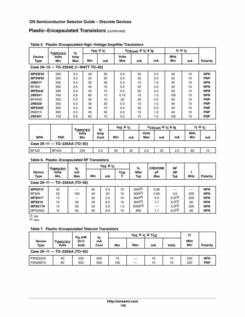
ON Semiconductor Selector Guide – Discrete Devices
http://onsemi.com 148
Plastic–Encapsulated Transistors (continued)
Table 5. Plastic–Encapsulated High–Voltage Amplifier Transistors
V(BR)CEO IChFE @ IC VCE(sat) @ IC & IB fT @ IC
DeviceType
V(BR)CEOVoltsMin
ICAmpMax Min mA
VoltsMax mA mA
MHzMin mA Polarity
Case 29–10 — TO–226AE (1–WATT TO–92)
MPSW42 300 0.5 40 30 0.5 20 2.0 50 10 NPNMPSW92 300 0.5 25 30 0.5 20 2.0 50 10 PNP2N6517 350 0.5 30 30 0.3 10 1.0 40 10 NPNBF393 300 0.5 40 10 0.2 20 2.0 50 10 NPNMPSA42 300 0.5 40 10 0.5 20 2.0 50 10 NPN2N5551 160 0.6 80 10 0.15 10 1.0 100 10 NPNBF493S 350 0.5 40 10 20 20 2.0 50 10 PNP2N6520 350 0.5 30 30 0.3 10 1.0 40 10 PNPMPSA92 300 0.5 40 10 0.5 20 2.0 50 10 PNP2N6519 300 0.5 45 30 0.3 10 1.0 40 10 PNP2N5401 150 0.6 60 10 0.2 10 1.0 100 10 PNP
V(BR)CEO IChFE @ IC VCE(sat) @ IC & IB fT @ IC
NPN PNP
V(BR)CEOVoltsMin
ICAmpCont Min mA
VoltsMax mA mA
MHzMin mA
Case 29–11 — TO–226AA (TO–92)
BF422 BF423 250 0.5 50 25 2.0 20 2.0 60 10
Table 6. Plastic–Encapsulated RF Transistors
V(BR)CEO IChFE @ IC fT CRE/CRB NF
DeviceType
V(BR)CEOVoltsMin
ICmAMax Min mA
VCEV
fTMHzTyp
CRE/CRBpF
Max
NFdBTyp
fMHz Polarity
Case 29–11 — TO–226AA (TO–92)
MPSH10 25 — 60 4.0 10 650(2) 0.65 — — NPNBF959 20 100 40 20 10 600(2) 0.65 3.0 200 NPNMPSH17 15 — 25 5.0 10 800(2) 0.9 6.0(3) 200 NPNMPS918 15 50 20 8.0 10 600(2) 1.7 6.0(3) 60 NPNMPS5179 12 50 25 3.0 1.0 2000(3) — 5.0(3) 200 NPNMPS3563 12 50 20 8.0 10 800 1.7 6.0(3) 60 NPN
(2) Min(3) Max
Table 7. Plastic–Encapsulated Telecom Transistors
PD mW IChFE @ IC @ VCE fT
DeviceType
V(BR)CEOVolts
PD mW25°CAmb
ICmA
Cont Min Max mA VoltsMHzMin Polarity
Case 29–11 — TO–226AA (TO–92)
P2N2222A 40 625 600 75 — 10 10 300 NPNP2N2907A 60 625 600 100 — 10 10 200 PNP

ON Semiconductor Selector Guide – Discrete Devices
http://onsemi.com 149
Plastic–Encapsulated Surface Mount Transistors
Table 8. Plastic–Encapsulated Surface Mount General–Purpose Transistors
hFE @ IC fTDevice Marking V(BR)CEO Min Max mA MHz Min Polarity
Case 318–08 — TO–236AB (SOT–23)
BC846ALT1 1A 65 110 220 2.0 100 NPNBC846BLT1 1B 65 200 450 2.0 100 NPNBC817–16LT1 6A 45 100 250 100 200 NPNBC817–25LT1 6B 45 160 400 100 200 NPNBC817–40LT1 6C 45 250 600 100 200 NPNBC847ALT1 1E 45 110 220 2.0 100 NPNBC847BLT1 1F 45 200 450 2.0 100 NPNBC847CLT1 1G 45 420 800 2.0 100 NPNMMBT2222ALT1 1P 40 100 300 150 200 NPNMMBT3904LT1 1AM 40 100 300 10 200 NPNMMBT4401LT1 2X 40 100 300 150 250 NPNBC848ALT1 1J 30 110 220 2.0 100 NPNBC848BLT1 1K 30 200 450 2.0 100 NPNBC848CLT1 1L 30 420 800 2.0 100 NPNBC856ALT1 3A 65 125 250 2.0 100 PNPBC856BLT1 3B 65 220 475 2.0 100 PNPMMBT2907ALT1 2F 60 100 300 150 200 PNPBC807–16LT1 5A 45 100 250 100 200 PNPBC807–25LT1 5B 45 160 400 100 200 PNPBC807–40LT1 5C 45 250 600 100 200 PNPBC857ALT1 3E 45 125 250 2.0 100 PNPBC857BLT1 3F 45 220 475 2.0 100 PNPMMBT3906LT1 2A 40 100 300 10 250 PNPMMBT4403LT1 2T 40 100 300 150 200 PNPBC858ALT1 3J 30 125 250 2.0 100 PNPBC858BLT1 3K 30 220 475 2.0 100 PNPBC858CLT1 3L 30 420 800 2.0 100 PNP
Case 318D–04 — SC–59
MSD601–RT1 YR 25 210 340 2.0 150(1) NPNMSD601–ST1 YS 25 290 460 2.0 150(1) NPNMSD602–RT1 WR 25 120 240 150 200(1) NPNMSD1328–RT1 1DR 20 200 350 500 200(1) NPNMSB709–RT1 AR 25 210 340 2.0 100(1) PNPMSB710–RT1 CR 25 120 240 150 200(1) PNP
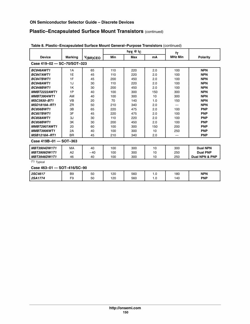
ON Semiconductor Selector Guide – Discrete Devices
http://onsemi.com 150
Plastic–Encapsulated Surface Mount Transistors (continued)
Table 8. Plastic–Encapsulated Surface Mount General–Purpose Transistors (continued)
hFE @ IC fTDevice Marking V(BR)CEO Min Max mA
fTMHz Min Polarity
Case 419–02 — SC–70/SOT–323
BC846AWT1 1A 65 110 220 2.0 100 NPNBC847AWT1 1E 45 110 220 2.0 100 NPNBC847BWT1 1F 45 200 450 2.0 100 NPNBC848AWT1 1J 30 110 220 2.0 100 NPNBC848BWT1 1K 30 200 450 2.0 100 NPNMMBT2222AWT1 1P 40 100 300 150 300 NPNMMBT3904WT1 AM 40 100 300 10 300 NPNMSC3930–BT1 VB 20 70 140 1.0 150 NPNMSD1819A–RT1 ZR 50 210 340 2.0 — NPNBC856BWT1 3B 65 220 475 2.0 100 PNPBC857BWT1 3F 45 220 475 2.0 100 PNPBC858AWT1 3J 30 110 220 2.0 100 PNPBC858BWT1 3K 30 200 450 2.0 100 PNPMMBT2907AWT1 20 60 100 300 150 200 PNPMMBT3906WT1 2A 40 100 300 10 250 PNPMSB1218A–RT1 BR 45 210 340 2.0 — PNP
Case 419B–01 — SOT–363
MBT3904DW1T1 MA 40 100 300 10 300 Dual NPNMBT3906DW1T1 A2 –40 100 300 10 250 Dual PNPMBT3946DW1T1 46 40 100 300 10 250 Dual NPN & PNP(1) Typical
Case 463–01 — SOT–416/SC–90
2SC4617 B9 50 120 560 1.0 180 NPN2SA1774 F9 50 120 560 1.0 140 PNP

ON Semiconductor Selector Guide – Discrete Devices
http://onsemi.com 151
Plastic–Encapsulated Surface Mount Transistors (continued)
Table 9. Plastic–Encapsulated Surface Mount Bias Resistor Transistors Table 13. for General Purpose Applications
These devices include bias resistors on the semiconductor chip with the transistor. See the BRT diagram fororientation of resistors.
Device Marking V(BR)CEOVolts
hFE@ IC ICmA R1 R2
NPN PNP NPN PNPVolts(Min) Min mA
mAMax
R1Ohm
R2Ohm
Case 318D–04 — SC–59
MUN2211T1 MUN2111T1 8A 6A 50 35 5.0 100 10K 10KMUN2212T1 MUN2112T1 8B 6B 50 60 5.0 100 22K 22KMUN2213T1 MUN2113T1 8C 6C 50 80 5.0 100 47K 47KMUN2214T1 MUN2114T1 8D 6D 50 80 5.0 100 10K 47KMUN2215T1 MUN2115T1 8E 6E 50 160 5.0 100 10K ∞MUN2216T1 MUN2116T1 8F 6F 50 160 5.0 100 4.7K ∞MUN2230T1 MUN2130T1 8G 6G 50 3.0 5.0 100 1.0K 1.0KMUN2231T1 MUN2131T1 8H 6H 50 8.0 5.0 100 2.2K 2.2KMUN2232T1 MUN2132T1 8J 6J 50 15 5.0 100 4.7K 4.7KMUN2233T1 MUN2133T1 8K 6K 50 80 5.0 100 4.7K 47KMUN2234T1 MUN2134T1 8L 6L 50 80 5.0 100 22K 47K
Case 318–08 — TO–236AB (SOT–23)
MMUN2211LT1 MMUN2111LT1 A8A A6A 50 35 5.0 100 10K 10KMMUN2212LT1 MMUN2112LT1 A8B A6B 50 60 5.0 100 22K 22KMMUN2213LT1 MMUN2113LT1 A8C A6C 50 80 5.0 100 47K 47KMMUN2214LT1 MMUN2114LT1 A8D A6D 50 80 5.0 100 10K 47KMMUN2215LT1 MMUN2115LT1 A8E A6E 50 160 5.0 100 10K ∞MMUN2216LT1 MMUN2116LT1 A8F A6F 50 160 5.0 100 4.7K ∞MMUN2230LT1 MMUN2130LT1 A8G A6G 50 3.0 5.0 100 1.0K 1.0KMMUN2231LT1 MMUN2131LT1 A8H A6H 50 8.0 5.0 100 2.2K 2.2KMMUN2232LT1 MMUN2132LT1 A8J A6J 50 15 5.0 100 4.7K 4.7KMMUN2233LT1 MMUN2133LT1 A8K A6K 50 80 5.0 100 4.7K 47KMMUN2234LT1 MMUN2134LT1 A8L A6L 50 80 5.0 100 22K 47K
Case 419–02 — SC–70/SOT–323
MUN5211T1 MUN5111T1 8A 6A 50 35 5.0 50 10K 10KMUN5212T1 MUN5112T1 8B 6B 50 60 5.0 50 22K 22KMUN5213T1 MUN5113T1 8C 6C 50 80 5.0 50 47K 47KMUN5214T1 MUN5114T1 8D 6D 50 80 5.0 50 10K 47KMUN5215T1 MUN5115T1 8E 6E 50 160 5.0 50 10K ∞MUN5216T1 MUN5116T1 8F 6F 50 160 5.0 50 4.7K ∞MUN5230T1 MUN5130T1 8G 6G 50 3.0 5.0 50 1.0K 1.0KMUN5231T1 MUN5131T1 8H 6H 50 8.0 5.0 50 2.2K 2.2KMUN5232T1 MUN5132T1 8J 6J 50 15 5.0 50 4.7K 4.7KMUN5233T1 MUN5133T1 8K 6K 50 80 5.0 50 4.7K 47KMUN5234T1 MUN5134T1 8L 6L 50 80 5.0 50 22K 47K
C(OUT)
E(GND)
B(IN)
R1
R2

ON Semiconductor Selector Guide – Discrete Devices
http://onsemi.com 152
Plastic–Encapsulated Surface Mount Transistors (continued)
Table 9. Plastic–Encapsulated Surface Mount Bias Resistor Transistorsfor General Purpose Applications (continued)
Device Marking V(BR)CEOVolts
hFE@ IC ICmA R1 R2
NPN PNP NPN PNPVolts(Min) Min mA
mAMax
R1Ohm
R2Ohm
Case 419B–01 — SOT–363 Duals
MUN5211DW1T1 MUN5111DW1T1 7A 8A 50 35 5.0 100 10K 10KMUN5212DW1T1 MUN5112DW1T1 7B 8B 50 60 5.0 100 22K 22KMUN5213DW1T1 MUN5113DW1T1 7C 8C 50 80 5.0 100 47K 47KMUN5214DW1T1 MUN5114DW1T1 7D 8D 50 80 5.0 100 10K 47KMUN5215DW1T1 MUN5115DW1T1 7E 8E 50 160 5.0 100 10K ∞MUN5216DW1T1 MUN5116DW1T1 7F 8F 50 160 5.0 100 4.7K ∞MUN5230DW1T1 MUN5130DW1T1 7G 8G 50 3.0 5.0 100 1.0K 1.0KMUN5231DW1T1 MUN5131DW1T1 7H 8H 50 8.0 5.0 100 2.2K 2.2KMUN5232DW1T1 MUN5132DW1T1 7J 8J 50 15 5.0 100 4.7K 4.7KMUN5233DW1T1 MUN5133DW1T1 7K 8K 50 80 5.0 100 4.7K 47KMUN5234DW1T1 MUN5134DW1T1 7L 8L 50 80 5.0 100 22K 47KMUN5235DW1T1 MUN5135DW1T1 7M 8M 50 80 5.0 100 2.2K 47K
hFE @ IC ICmA R1 R2
Device Marking V(BR)CEO Min mAmAMax
R1Ohm
R2Ohm
Case 419B–01 — SOT–363 — Dual Combination NPN and PNP
MUN5311DW1T1 11 50 35 5.0 100 10K 10KMUN5312DW1T1 12 50 60 5.0 100 22K 22KMUN5313DW1T1 13 50 80 5.0 100 47K 47KMUN5314DW1T1 14 50 80 5.0 100 10K 47KMUN5315DW1T1 15 50 160 5.0 100 10K ∞MUN5316DW1T1 16 50 160 5.0 100 4.7K ∞MUN5330DW1T1 3X 50 3.0 5.0 100 1.0K 1.0KMUN5331DW1T1 31 50 8.0 5.0 100 2.2K 2.2KMUN5332DW1T1 32 50 15 5.0 100 4.7K 4.7KMUN5333DW1T1 33 50 80 5.0 100 4.7K 47KMUN5334DW1T1 34 50 80 5.0 100 22K 47KMUN5335DW1T1 35 50 80 5.0 100 2.2K 47K
Device Marking V(BR)CEOVolts
hFE@ IC ICmA R1 R2
NPN PNP NPN PNPVolts(Min) Min mA
mAMax
R1Ohm
R2Ohm
Case 463–01 — SOT–416/SC–90
DTC114TE — 94 — 50 100 1.0 100 10K ∞DTC114YE DTA114YE 69 59 50 80 5.0 100 10K 47K
— DTA143EE — 43 50 15 5.0 100 4.7K 4.7K

ON Semiconductor Selector Guide – Discrete Devices
http://onsemi.com 153
Plastic–Encapsulated Surface Mount Transistors (continued)
Table 10. Plastic–Encapsulated Surface Mount VHF/UHF Amplifiers, Mixers, Oscillators
Ccb(13) fT @ IC
Device Marking V(BR)CEO
Ccb( )
pF Max GHz Min mA
Case 318–08 — TO–236AB (SOT–23) — NPN
MMBTH10LT1 3EM 25 0.7 0.65 4.0MMBT918LT1 M3B 15 1.7(14) 0.6 4.0
Case 318D–04 — SC–59 — NPN
MSC2295–BT1 VB 20 1.5(13) 0.15 1.0MSC2295–CT1 VC 20 1.5(13) 0.15 1.0MSC3130T1 1S 10 — 1.4 5.0(13) Cre(14) Cob
Table 11. Plastic–Encapsulated Surface Mount Darlingtons
VCE(sat) hFE @ IC
Device Marking V(BR)CES
CE(sat)Volts Max Min Max mA
Case 318–08 — TO–236AB (SOT–23) — NPN
MMBTA14LT1 1N 30 1.5 20K — 100
Case 318–08 — TO–236AB (SOT–23) — PNP
MMBTA64LT1 2V 30 1.5 20K — 100
Table 12. Plastic–Encapsulated Surface Mount Low–Noise Transistors
NFhFE@ IC fT
Device MarkingNF
dB Typ V(BR)CEO Min Max mAfT
MHz Min Polarity
Case 318–08 — TO–236AB (SOT–23)
MMBT5089LT1 1R 2.0(15) 25 400 — 10 50 NPNMMBT2484LT1 1U 3.0(15) 60 — 800 10 — NPNMMBT6428LT1 1KM 3.0 50 250 — 10 100 NPNMMBT6429LT1 1L 3.0 45 500 — 10 100 NPNMMBT5087LT1 2Q 2.0(15) 50 250 — 10 40 PNP
(15) Max
Table 13. Plastic–Encapsulated Surface Mount High–Voltage Transistors
hFE@ IC fTDevice Marking V(BR)CEO Min Max mA
fTMHz Min Polarity
Case 318–08 — TO–236AB (SOT–23)
MMBT6517LT1 1Z 350 15 — 100 40 NPNMMBTA42LT1 1D 300 40 — 30 50 NPNMMBT5551LT1 G1 160 30 — 50 100 NPNMMBT6520LT1 2Z 350 15 — 100 40 PNPMMBTA92LT1 2D 300 25 — 30 50 PNPMMBT5401LT1 2L 150 50 — 50 100 PNP
Table 14. Plastic–Encapsulated Surface Mount Drivers
hFE@ IC
Device Marking V(BR)CEO VCE(sat) VBE(sat) Min Max mA Polarity
Case 318–08 — TO–236AB (SOT–23)
MMBTA06LT1 1GM 80 0.25 — 100 — 100 NPNBSS64LT1 AM 80 0.15 — 20 — 10 NPNBSS63LT1 T1 100 –0.25 –0.90 30 — 25 PNPMMBTA56LT1 2GM 80 –0.25 — 100 — 100 PNP
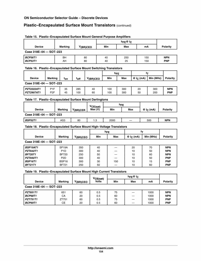
ON Semiconductor Selector Guide – Discrete Devices
http://onsemi.com 154
Plastic–Encapsulated Surface Mount Transistors (continued)
Table 15. Plastic–Encapsulated Surface Mount General Purpose Amplifiers
hFE@ IC
Device Marking V(BR)CEO Min Max mA Polarity
Case 318E–04 — SOT–223
BCP56T1 BH 80 40 250 150 NPNBCP53T1 AH 80 40 25 150 PNP
Table 16. Plastic–Encapsulated Surface Mount Switching Transistors
hFE fT
Device Marking ton toff V(BR)CEO Min Max @ IC (mA) Min (MHz) Polarity
Case 318E–04 — SOT–223
PZT2222AT1 P1F 35 285 40 100 300 20 300 NPNPZT2907AT1 P2F 45 100 60 100 300 50 200 PNP
Table 17. Plastic–Encapsulated Surface Mount Darlingtons
VCE(sat)hFE
Device Marking V(BR)CER
VCE(sat)Max (V) Min Max @ IC (mA) Polarity
Case 318E–04 — SOT–223
BSP52T1 AS3 80 1.3 2000 — 500 NPN
Table 18. Plastic–Encapsulated Surface Mount High–Voltage Transistors
hFE fT
Device Marking V(BR)CEO Min Max @ IC (mA) Min (MHz) Polarity
Case 318E–04 — SOT–223
BSP19AT1 SP19A 350 40 — 20 70 NPNPZTA42T1 P1D 300 40 — 10 50 NPNBF720T1 BF720 250 50 — 10 60 NPNPZTA92T1 P2D 300 40 — 10 50 PNPBSP16T1 BSP16 300 30 150 10 15 PNPBF721T1 BF721 250 50 — 10 60 PNP
Table 19. Plastic–Encapsulated Surface Mount High Current Transistors
VCE(sat)hFE@ IC
Device Marking V(BR)CEO
VCE(sat)Volts Min Max mA Polarity
Case 318E–04 — SOT–223
PZT651T1 651 60 0.5 75 — 1000 NPNBCP68T1 CA 20 0.5 60 — 1000 NPNPZT751T1 ZT751 60 0.5 75 — 1000 PNPBCP69T1 CE 20 0.5 60 — 1000 PNP

ON Semiconductor Selector Guide – Discrete Devices
http://onsemi.com 155
Field–Effect Transistors
JFETs
Table 20. JFET Low–Frequency/Low–Noise
Re Yfs @ f Re Yos @ fCiss Crss
V(BR)GSSV(BR)GDO
VGS(off)Volts
IDSSmA
Devicemmho
Min kHzµmhoMax kHz
CisspF
Max
CrsspF
Max
V(BR)GDOVoltsMin Min Max Min Max Polarity
Case 29–11 — TO–226AA (TO–92)
2N5457 1.0 1.0 50 1.0 7.0 3.0 25 0.5 6.0 1.0 5.0 N–Channel2N5458 1.5 1.0 50 1.0 7.0 3.0 25 1.0 7.0 2.0 9.0 N–Channel2N5460 1.0 1.0 75 1.0 7.0 2.0 40 0.75 6.0 1.0 5.0 P–Channel2N5461 1.5 1.0 75 1.0 7.0 2.0 40 1.0 7.5 2.0 9.0 P–Channel2N5462 2.0 1.0 75 1.0 7.0 2.0 40 1.8 9.0 4.0 16 P–Channel
Table 21. JFET High–Frequency Amplifiers
Re Yfs @ f Re Yos @ fCiss Crss
NF @ RG = 1K V(BR)GSSV(BR)GDO
VGS(off)Volts
IDSSmA
Devicemmho
Min MHzµmhoMax MHz
CisspF
Max
CrsspF
MaxdB
Maxf
MHz
V(BR)GDOVoltsMin Min Max Min Max Polarity
Case 29–11 — TO–226AA (TO–92)
MPF102 1.6 100 200 100 7.0 3.0 — — 25 — 8.0 2.0 20 N–Channel2N5485 3.0 400 100 400 5.0 1.0 4.0 400 25 0.5 4.0 4.0 10 N–Channel2N5486 3.5 400 100 400 5.0 1.0 4.0 400 25 2.0 6.0 8.0 20 N–ChannelJ309 12(1) 100 250(1) 100 7.5 2.5 1.5(1) 100 25 1.0 4.0 12 30 N–ChannelJ310 12(1) 100 250(1) 100 7.5 2.5 1.5(1) 100 25 2.0 6.5 24 60 N–Channel
(1) Typical
Table 22. JFET Switches and Choppers
RDS(on) @ ID
VGS(off)Volts
IDSSmA V(BR)GSS
V(BR)GDO Ciss Crss ton toff
DeviceΩ
Max mA Min Max Min Max
V(BR)GDOVoltsMin
CisspF
Max
CrsspF
Max
tonns
Max
toffns
Max Polarity
Case 29–11 — TO–226AA (TO–92)
J112 50 — 1.0 5.0 5.0 — 35 28 5.0 — — N–ChannelMPF4392 60 — — — 25 75 30 10 3.5 15 35 N–Channel2N5639 60 1.0 — (8.0)(1) 25 — 30 10 4.0 — — N–ChannelMPF4393 100 — — (12)(1) 5.0 30 30 10 3.5 15 55 N–ChannelJ110 18 — 0.5 4.0 10 — 25 — — — — N–Channel
(1) Typical(16) VGS(f)
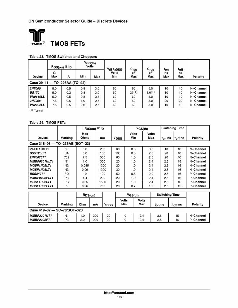
ON Semiconductor Selector Guide – Discrete Devices
http://onsemi.com 156
Table 23. TMOS Switches and Choppers
RDS(on) @ ID
VGS(th)Volts
V(BR)DSS Ciss Crss ton toff
DeviceΩ
Max A Min Max
V(BR)DSSVoltsMin
CisspF
Max
CrsspF
Max
tonns
Max
toffns
Max Polarity
Case 29–11 — TO–226AA (TO–92)
2N7000 5.0 0.5 0.8 3.0 60 60 5.0 10 10 N–ChannelBS170 5.0 0.2 0.8 3.0 60 25(1) 3.0(1) 10 10 N–ChannelVN0610LL 5.0 0.5 0.8 2.5 60 60 5.0 10 10 N–Channel2N7008 7.5 0.5 1.0 2.5 60 50 5.0 20 20 N–ChannelVN2222LL 7.5 0.5 0.6 2.5 60 60 5.0 10 10 N–Channel
(1) Typical
Table 24. TMOS FETs
RDS(on) @ ID VGS(th) Switching Time
Device MarkingMax
Ohms mA VDSS
VoltsMin
VoltsMax ton ns toff ns Polarity
Case 318–08 — TO–236AB (SOT–23)
MMBF170LT1 6Z 5.0 200 60 0.8 3.0 10 10 N–ChannelBSS123LT1 SA 6.0 100 100 0.8 2.8 20 40 N–Channel2N7002LT1 702 7.5 500 60 1.0 2.5 20 40 N–ChannelMMBF0201NLT1 N1 1.0 300 20 1.0 2.4 2.5 15 N–ChannelMGSF1N02LT1 N2 0.085 1200 20 1.0 2.4 2.5 16 N–ChannelMGSF1N03LT1 N3 0.09 1200 30 1.0 2.4 2.5 16 N–ChannelBSS84LT1 PD 10 100 50 0.8 2.0 2.5 16 P–ChannelMMBF0202PLT1 P3 1.4 200 20 1.0 2.4 2.5 16 P–ChannelMGSF1P02LT1 PC 0.35 1500 20 1.0 2.4 2.5 16 P–ChannelMGSF1P02ELT1 PE 0.26 750 20 0.7 1.2 2.5 15 P–Channel
RDS(on) VGS(th) Switching Time
Device Marking Ohm mA VDSS
VoltsMin
VoltsMax ton ns toff ns Polarity
Case 419–02 — SC–70/SOT–323
MMBF2201NT1 N1 1.0 300 20 1.0 2.4 2.5 15 N–ChannelMMBF2202PT1 P3 2.2 200 20 1.0 2.4 2.5 16 P–Channel
TMOS FETs
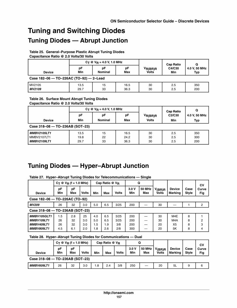
ON Semiconductor Selector Guide – Discrete Devices
http://onsemi.com 157
Tuning and Switching DiodesTuning Diodes — Abrupt Junction
Table 25. General–Purpose Plastic Abrupt Tuning DiodesCapacitance Ratio @ 2.0 Volts/30 Volts
CT @ VR = 4.0 V, 1.0 MHzCap Ratio Q
DevicepFMin
pFNominal
pFMax
VR(BR)RVolts
Cap RatioC4/C30
Min
Q4.0 V, 50 MHz
Typ
Case 182–06 — TO–226AC (TO–92) — 2–Lead
MV2105 13.5 15 16.5 30 2.5 350MV2109 29.7 33 36.3 30 2.5 200
Table 26. Surface Mount Abrupt Tuning DiodesCapacitance Ratio @ 2.0 Volts/30 Volts
CT @ VR = 4.0 V, 1.0 MHzCap Ratio Q
Device
pF
Min
pF
Nominal
pF
Max
VR(BR)RVolts
Cap RatioC2/C30
Min
4.0 V, 50 MHz
Typ
Case 318–08 — TO–236AB (SOT–23)
MMBV2105LT1 13.5 15 16.5 30 2.5 350MMBV2107LT1 19.8 22 24.2 30 2.5 300MMBV2109LT1 29.7 33 36.3 30 2.5 200
Tuning Diodes — Hyper–Abrupt Junction
Table 27. Hyper–Abrupt Tuning Diodes for Telecommunications — Single
CT @ VR (f = 1.0 MHz) Cap Ratio @ VR QCV
DevicepFMin
pFMax Volts Min Max Volts
3.0 VMin
50 MHzMax
V(BR)RVolts
DeviceMarking
CaseStyle
CVCurve
Fig
Case 182–06 — TO–226AC (TO–92)
MV209 26 32 3.0 5.0 6.5 3/25 200 — 30 — 1 2
Case 318–08 — TO–236AB (SOT–23)
MMBV105GLT1 1.5 2.8 25 4.0 6.5 3/25 200 — 30 M4E 8 1MMBV109LT1 26 32 3.0 5.0 6.5 3/25 200 — 30 M4A 8 2MMBV409LT1 26 32 3.0 1.5 1.9 3/8 200 — 20 X5 8 3MMBV809LT1 4.5 6.1 2.0 1.8 2.6 2/8 300 — 20 5K 8 4
Table 28. Hyper–Abrupt Tuning Diodes for Communications — Dual
CT @ VR (f = 1.0 MHz) Cap Ratio @ VR QCV
DevicepFMin
pFMax Volts Min Max Volts
3.0 VMin
50 MHzMax
V(BR)RVolts
DeviceMarking
CaseStyle
CVCurve
Fig
Case 318–08 — TO–236AB (SOT–23)
MMBV609LT1 26 32 3.0 1.8 2.4 3/8 250 — 20 5L 9 6

ON Semiconductor Selector Guide – Discrete Devices
http://onsemi.com 158
Schottky Diodes
Table 29. Schottky Diodes
V(BR)RCT @ VR
pFVF @ 10 mA
VoltsIR @ VR
nAMinorityLifetime Device
DeviceV(BR)R
VoltspF
MaxVoltsMax
nAMax
LifetimepS (TYP)
DeviceMarking
Case 182–06 — TO–226AC (TO–92)MBD701 70 1.0 @ 20 V 1.0 200 @ 35 V 15 —MBD301 30 1.5 @ 15 V 0.6 200 @ 25 V 15 —
Case 318–08 — TO–236AB (SOT–23) – SingleBAS40LT1 40 5.0 @ 1.0 V 0.5 @ 30 mA 1000 @ 25 V — B1BAS40–04LT1 40 5.0 @ 1.0 V 0.5 @ 30 mA 1000 @ 25 V — —BAS70LT1 70 2.0 @ 0 V 0.75 100 @ 50 V — BEBAT54ALT1 30 10 @ 1.0 V 0.4 2000 @ 25 V — —BAT54LT1 30 10 @ 1.0 V 0.4 2000 @ 25 V — LV3BAT54SLT1 30 10 @ 1.0 V 0.4 2000 @ 25 V — LD3MMBD701LT1 70 1.0 @ 20 V 1.0 200 @ 35 V 15 5HMMBD301LT1 30 1.5 @ 15 V 0.6 200 @ 25 V 15 4T
Case 318–08 — TO–236AB (SOT–23) – DualBAS40–06LT1 40 5.0 @ 1.0 V 0.5 @ 30 mA 1000 @ 25 V — —BAS70–04LT1(23) 70 2.0 @ 0 V 0.75 100 @ 50 V — —MMBD452LT1 30 1.5 @ 1.5 V 0.6 200 @ 25 V 15 5N
Case 425–04 — (SOD–123)BAT54T1 30 10 @ 1.0 V 0.4 2000 @ 25 V — —MMSD301T1 30 1.5 @ 15 V 0.6 0.2 @ 25 V 15 XT
Case 419–02 — (SC–70/SOT–323) – SingleBAT54WT1 30 10 @ 1.0 V 0.4 2000 @ 25 V — —MMBD330T1 30 1.5 @ 15 V 0.6 0.2 @ 25 V — —MMBD770T1 70 1.0 @ 20 V 1.0 0.2 @ 35 V — —
Case 419–02 — (SC–70/SOT–323) – DualBAT54SWT1 30 10 @ 1.0 V 0.4 2000 @ 25 V — —MMBD717LT1(23) 20 2.5 @ 1.0 V 0.37 @ 1 mA 0.2 @ 10 V — B3(23) Common Anode
Case 419B–01 — SOT–363 – DualsV(BR)R IR VF CT(30) trr
Device MarkingMin
Volts@ IBR(µA)
Max(µA)
@ VRVolts
MinVolts
MaxVolts
@ IF(mA)
CT( )
Max(pF)
trrMax(ns)
MBD54DWT1 BL 30 10 2.0 25 — 0.32 1.0 1.0 5.0MBD330DWT1 T4 30 10 200 25 — 0.4 1.0 1.5 —MBD770DWT1 H5 70 10 200 25 — 0.5 1.0 1.0 —(30) VR = 0 V, f = 1.0 MHz
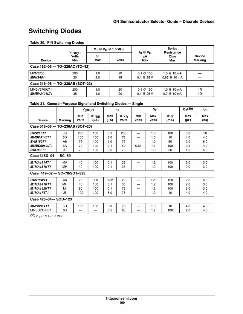
ON Semiconductor Selector Guide – Discrete Devices
http://onsemi.com 159
Switching Diodes
Table 30. PIN Switching Diodes
V(BR)RCT @ VR @ 1.0 MHz
IR @ VRSeries
Resistance
Device
V(BR)RVoltsMin
pFMax Volts
IR @ VRµA
Max
ResistanceOhmMax
DeviceMarking
Case 182–06 — TO–226AC (TO–92)
MPN3700 200 1.0 20 0.1 @ 150 1.0 @ 10 mA —MPN3404 20 2.0 15 0.1 @ 25 V 0.85 @ 10 mA —
Case 318–08 — TO–236AB (SOT–23)
MMBV3700LT1 200 1.0 20 0.1 @ 150 1.0 @ 10 mA 4RMMBV3401LT1 35 1.0 20 0.1 @ 25 V 0.7 @ 10 mA 4D
Table 31. General–Purpose Signal and Switching Diodes — Single
V(BR)R IR VF CT(30) trr
Device MarkingMin
Volts@ IBR(µA)
Max(µA)
@ VRVolts
MinVolts
MaxVolts
@ IF(mA)
Max(pF)
Max(ns)
Case 318–08 — TO–236AB (SOT–23)
BAS21LT1 JS 250 100 0.1 200 — 1.0 100 5.0 50MMBD914LT1 5D 100 100 5.0 75 — 1.0 10 4.0 4.0BAS16LT1 A6 75 100 1.0 75 — 1.0 50 2.0 6.0MMBD6050LT1 5A 70 100 0.1 50 0.85 1.1 100 2.5 4.0BAL99LT1 JF 70 100 2.5 70 — 1.0 50 1.5 6.0
Case 318D–04 — SC–59
M1MA151AT1 MA 40 100 0.1 35 — 1.2 100 2.0 3.0M1MA151KT1 MH 40 100 0.1 35 — 1.2 100 2.0 3.0
Case 419–02 — SC–70/SOT–323
BAS16WT1 A6 75 1.0 0.02 20 — 1.25 150 2.0 6.0M1MA141KT1 MH 40 100 0.1 35 — 1.2 100 2.0 3.0M1MA142KT1 MI 80 100 0.1 75 — 1.2 100 2.0 3.0M1MA174T1 J6 100 100 5.0 75 — 1.0 10 4.0 4.0
Case 425–04— SOD–123
MMSD914T1 5D 100 100 5.0 75 — 1.0 10 4.0 4.0MMSD71RKT1 6S — — 0.5 80 — 1.2 100 2.0 4.0
(30) VR = 0 V, f = 1.0 MHz
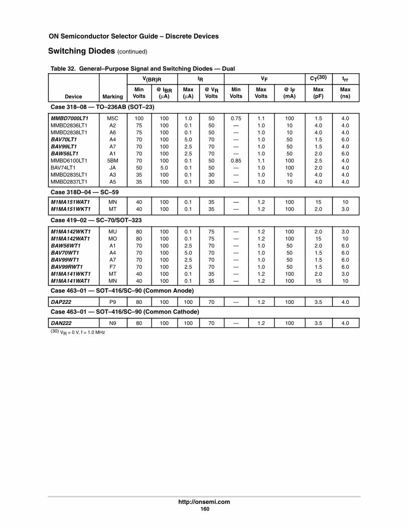
ON Semiconductor Selector Guide – Discrete Devices
http://onsemi.com 160
Switching Diodes (continued)
Table 32. General–Purpose Signal and Switching Diodes — Dual
V(BR)R IR VF CT(30) trr
Device MarkingMin
Volts@ IBR(µA)
Max(µA)
@ VRVolts
MinVolts
MaxVolts
@ IF(mA)
Max(pF)
Max(ns)
Case 318–08 — TO–236AB (SOT–23)
MMBD7000LT1 M5C 100 100 1.0 50 0.75 1.1 100 1.5 4.0MMBD2836LT1 A2 75 100 0.1 50 — 1.0 10 4.0 4.0MMBD2838LT1 A6 75 100 0.1 50 — 1.0 10 4.0 4.0BAV70LT1 A4 70 100 5.0 70 — 1.0 50 1.5 6.0BAV99LT1 A7 70 100 2.5 70 — 1.0 50 1.5 4.0BAW56LT1 A1 70 100 2.5 70 — 1.0 50 2.0 6.0MMBD6100LT1 5BM 70 100 0.1 50 0.85 1.1 100 2.5 4.0BAV74LT1 JA 50 5.0 0.1 50 — 1.0 100 2.0 4.0MMBD2835LT1 A3 35 100 0.1 30 — 1.0 10 4.0 4.0MMBD2837LT1 A5 35 100 0.1 30 — 1.0 10 4.0 4.0
Case 318D–04 — SC–59
M1MA151WAT1 MN 40 100 0.1 35 — 1.2 100 15 10M1MA151WKT1 MT 40 100 0.1 35 — 1.2 100 2.0 3.0
Case 419–02 — SC–70/SOT–323
M1MA142WKT1 MU 80 100 0.1 75 — 1.2 100 2.0 3.0M1MA142WAT1 MO 80 100 0.1 75 — 1.2 100 15 10BAW56WT1 A1 70 100 2.5 70 — 1.0 50 2.0 6.0BAV70WT1 A4 70 100 5.0 70 — 1.0 50 1.5 6.0BAV99WT1 A7 70 100 2.5 70 — 1.0 50 1.5 6.0BAV99RWT1 F7 70 100 2.5 70 — 1.0 50 1.5 6.0M1MA141WKT1 MT 40 100 0.1 35 — 1.2 100 2.0 3.0M1MA141WAT1 MN 40 100 0.1 35 — 1.2 100 15 10
Case 463–01 — SOT–416/SC–90 (Common Anode)
DAP222 P9 80 100 100 70 — 1.2 100 3.5 4.0
Case 463–01 — SOT–416/SC–90 (Common Cathode)
DAN222 N9 80 100 100 70 — 1.2 100 3.5 4.0(30) VR = 0 V, f = 1.0 MHz
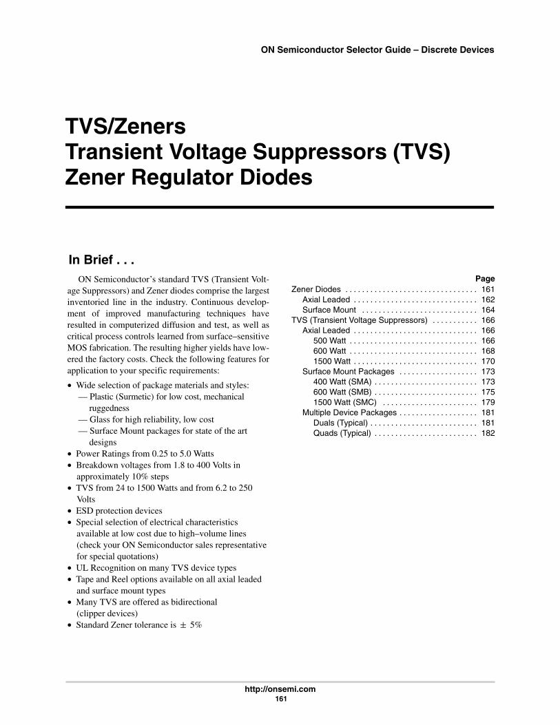
ON Semiconductor Selector Guide – Discrete Devices
http://onsemi.com 161
TVS/ZenersTransient Voltage Suppressors (TVS)Zener Regulator Diodes
In Brief . . .Page
Zener Diodes 161. . . . . . . . . . . . . . . . . . . . . . . . . . . . . . . . Axial Leaded 162. . . . . . . . . . . . . . . . . . . . . . . . . . . . . . Surface Mount 164. . . . . . . . . . . . . . . . . . . . . . . . . . . .
TVS (Transient Voltage Suppressors) 166. . . . . . . . . . . Axial Leaded 166. . . . . . . . . . . . . . . . . . . . . . . . . . . . . .
500 Watt 166. . . . . . . . . . . . . . . . . . . . . . . . . . . . . . . 600 Watt 168. . . . . . . . . . . . . . . . . . . . . . . . . . . . . . . 1500 Watt 170. . . . . . . . . . . . . . . . . . . . . . . . . . . . . .
Surface Mount Packages 173. . . . . . . . . . . . . . . . . . . 400 Watt (SMA) 173. . . . . . . . . . . . . . . . . . . . . . . . . 600 Watt (SMB) 175. . . . . . . . . . . . . . . . . . . . . . . . . 1500 Watt (SMC) 179. . . . . . . . . . . . . . . . . . . . . . .
Multiple Device Packages 181. . . . . . . . . . . . . . . . . . . Duals (Typical) 181. . . . . . . . . . . . . . . . . . . . . . . . . . Quads (Typical) 182. . . . . . . . . . . . . . . . . . . . . . . . .
ON Semiconductor’s standard TVS (Transient Volt-age Suppressors) and Zener diodes comprise the largestinventoried line in the industry. Continuous develop-ment of improved manufacturing techniques haveresulted in computerized diffusion and test, as well ascritical process controls learned from surface–sensitiveMOS fabrication. The resulting higher yields have low-ered the factory costs. Check the following features forapplication to your specific requirements:
• Wide selection of package materials and styles:— Plastic (Surmetic) for low cost, mechanical
ruggedness— Glass for high reliability, low cost— Surface Mount packages for state of the art
designs• Power Ratings from 0.25 to 5.0 Watts• Breakdown voltages from 1.8 to 400 Volts in
approximately 10% steps• TVS from 24 to 1500 Watts and from 6.2 to 250
Volts• ESD protection devices• Special selection of electrical characteristics
available at low cost due to high–volume lines(check your ON Semiconductor sales representativefor special quotations)
• UL Recognition on many TVS device types• Tape and Reel options available on all axial leaded
and surface mount types• Many TVS are offered as bidirectional
(clipper devices)• Standard Zener tolerance is 5%

ON Semiconductor Selector Guide – Discrete Devices
http://onsemi.com 162
Zener Diodes — Regulation in Axial Leads
Table 1. Axial Leaded — .5, 1, 1.3, 1.5, 3 and 5 Watt
Nominal 500 mWLow Level
1 Watt 1.3 Watt 1.5 Watt 5 Watt
ZenerB kd
Low LevelCathode = 500 mW Cathode =Breakdown
Voltage
Cathode =Polarity Cathode = Polarity Band Cathode = Cathode = Cathode =
Cathode =PolarityVoltage y
Band Polarity Band Polarity Band Polarity Bandy
Band
Volts
GlassCase 299
DO-204AH(DO-35)
GlassCase 59-03
(DO-41)
PlasticSurmetic 30Case 59-03
(DO-41)
GlassCase 59-03
(DO-41)
PlasticSurmetic 30Case 59-03
(DO-41)
PlasticSurmetic 40
Case 17
1.8 1N46782.0 1N46792.2 1N46802.4 1N4681 1N5221B BZX79C2V4RL2.5 1N5222B
2.7 1N4682 1N5223B BZX79C2V7RL2.8 1N5224B3.0 1N4683 1N5225B BZX79C3V0RL3.3 1N4684 1N5226B BZX79C3V3RL 1N4728A MZP4728A BZX85C3V3RL 1N5913B 1N5333B3.6 1N4685 1N5227B BZX79C3V6RL 1N4729A MZP4729A BZX85C3V6RL 1N5914B 1N5334B
3.9 1N4686 1N5228B BZX79C3V9RL 1N4730A MZP4730A BZX85C3V9RL 1N5915B 1N5335B4.3 1N4687 1N5229B BZX79C4V3RL 1N4731A MZP4731A BZX85C4V3RL 1N5916B 1N5336B4.7 1N4688 1N5230B BZX79C4V7RL 1N4732A MZP4732A BZX85C4V7RL 1N5917B 1N5337B5.1 1N4689 1N5231B BZX79C5V1RL 1N4733A MZP4733A BZX85C5V1RL 1N5918B 1N5338B5.6 1N4690 1N5232B BZX79C5V6RL 1N4734A MZP4734A BZX85C5V6RL 1N5919B 1N5339B
6.0 1N5233B 1N5340B6.2 1N4691 1N5234B BZX79C6V2RL 1N4735A MZP4735A BZX85C6V2RL 1N5920B 1N5341B6.8 1N4692 1N5235B BZX79C6V8RL 1N4736A MZP4736A BZX85C6V8RL 1N5921B 1N5342B7.5 1N4693 1N5236B BZX79C7V5RL 1N4737A MZP4737A BZX85C7V5RL 1N5922B 1N5343B8.2 1N4694 1N5237B BZX79C8V2RL 1N4738A MZP4738A BZX85C8V2RL 1N5923B 1N5344B
8.7 1N4695 1N5238B 1N5345B9.1 1N4696 1N5239B BZX79C9V1RL 1N4739A MZP4739A BZX85C9V1RL 1N5924B 1N5346B10 1N4697 1N5240B BZX79C10RL 1N4740A MZP4740A BZX85C10RL 1N5925B 1N5347B11 1N4698 1N5241B BZX79C11RL 1N4741A MZP4741A BZX85C11RL 1N5926B 1N5348B12 1N4699 1N5242B BZX79C12RL 1N4742A MZP4742A BZX85C12RL 1N5927B 1N5349B
13 1N4700 1N5243B BZX79C13RL 1N4743A MZP4743A BZX85C13RL 1N5928B 1N5350B14 1N4701 1N5244B 1N5351B15 1N4702 1N5245B BZX79C15RL 1N4744A MZP4744A BZX85C15RL 1N5929B 1N5352B16 1N4703 1N5246B BZX79C16RL 1N4745A MZP4745A BZX85C16RL 1N5930B 1N5353B17 1N4704 1N5247B 1N5354B
18 1N4705 1N5248B BZX79C18RL 1N4746A MZP4746A BZX85C18RL 1N5931B 1N5355B19 1N4706 1N5249B 1N5356B20 1N4707 1N5250B BZX79C20RL 1N4747A MZP4747A BZX85C20RL 1N5932B 1N5357B22 1N4708 1N5251B BZX79C22RL 1N4748A MZP4748A BZX85C22RL 1N5933B 1N5358B24 1N4709 1N5252B BZX79C24RL 1N4749A MZP4749A BZX85C24RL 1N5934B 1N5359B
Devices listed in bold, italic are ON Semiconductor preferred devices.
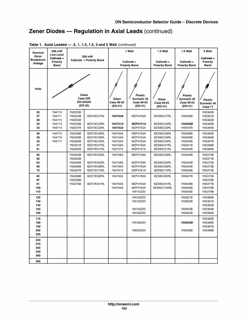
ON Semiconductor Selector Guide – Discrete Devices
http://onsemi.com 163
Zener Diodes — Regulation in Axial Leads (continued)
Table 1. Axial Leaded — .5, 1, 1.3, 1.5, 3 and 5 Watt (continued)
Nominal 500 mWLow Level
1 Watt 1.3 Watt 1.5 Watt 5 Watt
ZenerB kd
Low LevelCathode = 500 mW Cathode =Breakdown
Voltage
Cathode =Polarity Cathode = Polarity Band Cathode = Cathode = Cathode =
Cathode =PolarityVoltage y
Band Polarity Band Polarity Band Polarity Bandy
Band
Volts
GlassCase 299
DO-204AH(DO-35)
GlassCase 59-03
(DO-41)
PlasticSurmetic 30Case 59-03
(DO-41)
GlassCase 59-03
(DO-41)
PlasticSurmetic 30Case 59-03
(DO-41)
PlasticSurmetic 40
Case 17
25 1N4710 1N5253B 1N5360B27 1N4711 1N5254B BZX79C27RL 1N4750A MZP4750A BZX85C27RL 1N5935B 1N5361B28 1N4712 1N5255B 1N5362B30 1N4713 1N5256B BZX79C30RL 1N4751A MZP4751A BZX85C30RL 1N5936B 1N5363B33 1N4714 1N5257B BZX79C33RL 1N4752A MZP4752A BZX85C33RL 1N5937B 1N5364B
36 1N4715 1N5258B BZX79C36RL 1N4753A MZP4753A BZX85C36RL 1N5938B 1N5365B39 1N4716 1N5259B BZX79C39RL 1N4754A MZP4754A BZX85C39RL 1N5939B 1N5366B43 1N4717 1N5260B BZX79C43RL 1N4755A MZP4755A BZX85C43RL 1N5940B 1N5367B47 1N5261B BZX79C47RL 1N4756A MZP4756A BZX85C47RL 1N5941B 1N5368B51 1N5262B BZX79C51RL 1N4757A MZP4757A BZX85C51RL 1N5942B 1N5369B
56 1N5263B BZX79C56RL 1N4758A MZP4758A BZX85C56RL 1N5943B 1N5370B60 1N5264B 1N5371B62 1N5265B BZX79C62RL 1N4759A MZP4759A BZX85C62RL 1N5944B 1N5372B68 1N5266B BZX79C68RL 1N4760A MZP4760A BZX85C68RL 1N5945B 1N5373B75 1N5267B BZX79C75RL 1N4761A MZP4761A BZX85C75RL 1N5946B 1N5374B
82 1N5268B BZX79C82RL 1N4762A MZP4762A BZX85C82RL 1N5947B 1N5375B87 1N5269B 1N5376B91 1N5270B BZX79C91RL 1N4763A MZP4763A BZX85C91RL 1N5948B 1N5377B100 1N4764A MZP4764A BZX85C100RL 1N5949B 1N5378B110 1M110ZS5 1N5950B 1N5379B
120 1M120ZS5 1N5951B 1N5380B130 1M130ZS5 1N5952B 1N5381B140 1N5382B150 1M150ZS5 1N5953B 1N5383B160 1M160ZS5 1N5954B 1N5384B
170 1N5385B180 1M180ZS5 1N5955B 1N5386B190 1N5387B200 1M200ZS5 1N5956B 1N5388B220
240270300330360
400

ON Semiconductor Selector Guide – Discrete Devices
http://onsemi.com 164
Zener Diodes — Regulation in Surface Mount
Table 2. Surface Mount Packages — .2, .225, .5, 1.5, 3 Watt
Nom–inal
200 mW 225 mW 500 mW 1.5 Watt 3 Watt
ZenerBreak–down
VoltageSOD–323 SOT-23 SOD-123 SMA SMB
Volts
Case 477Style 1
PlasticCase 318TO-236AB
AnodeCathode
No Connection
PlasticCase 425, Style 1
PlasticCase 403ACathode =
Notch
PlasticCase 403B
ÁÁÁÁÁÁÁÁ
1.8 ÁÁÁÁÁÁÁÁ
ÁÁÁÁÁÁÁÁ
ÁÁÁÁÁÁÁÁÁÁ
ÁÁÁÁÁÁÁÁ
ÁÁÁÁÁÁÁÁÁÁ
MMSZ4678T1ÁÁÁÁÁÁÁÁ
ÁÁÁÁÁÁÁÁÁÁ
ÁÁÁÁÁÁÁÁÁÁÁÁ
2.0ÁÁÁÁÁÁÁÁÁÁÁÁÁÁÁÁÁÁÁÁÁÁ
MMSZ4679T1ÁÁÁÁÁÁÁÁÁÁÁÁÁÁÁÁÁ
ÁÁÁÁ2.2 ÁÁÁÁÁÁÁÁ
ÁÁÁÁÁÁÁÁ
ÁÁÁÁÁÁÁÁÁÁ
ÁÁÁÁÁÁÁÁ
ÁÁÁÁÁÁÁÁÁÁ
MMSZ4680T1ÁÁÁÁÁÁÁÁ
ÁÁÁÁÁÁÁÁÁÁ
ÁÁÁÁÁÁÁÁÁÁÁÁ2.4 ÁÁÁÁMM3Z2V4T1ÁÁÁÁBZX84C2V4LT1ÁÁÁÁÁMMBZ5221BLT1ÁÁÁÁMMSZ2V4T1ÁÁÁÁÁMMSZ4681T1ÁÁÁÁMMSZ5221BT1ÁÁÁÁÁÁÁÁÁÁÁÁÁ
ÁÁÁÁ2.5ÁÁÁÁÁÁÁÁ
ÁÁÁÁÁÁÁÁ
ÁÁÁÁÁÁÁÁÁÁ
MMBZ5222BLT1ÁÁÁÁÁÁÁÁ
ÁÁÁÁÁÁÁÁÁÁ
ÁÁÁÁÁÁÁÁ
MMSZ5222BT1ÁÁÁÁÁÁÁÁÁÁ
ÁÁÁÁÁÁÁÁÁÁÁÁ
ÁÁÁÁ2.7 ÁÁÁÁÁÁÁÁ
ÁÁÁÁÁÁÁÁ
BZX84C2V7LT1ÁÁÁÁÁÁÁÁÁÁ
MMBZ5223BLT1ÁÁÁÁÁÁÁÁ
MMSZ2V7T1ÁÁÁÁÁÁÁÁÁÁ
MMSZ4682T1ÁÁÁÁÁÁÁÁ
MMSZ5223BT1ÁÁÁÁÁÁÁÁÁÁ
ÁÁÁÁÁÁÁÁÁÁÁÁ
ÁÁÁÁ2.8 ÁÁÁÁÁÁÁÁ
ÁÁÁÁÁÁÁÁ
ÁÁÁÁÁÁÁÁÁÁ
MMBZ5224BLT1ÁÁÁÁÁÁÁÁ
ÁÁÁÁÁÁÁÁÁÁ
ÁÁÁÁÁÁÁÁ
MMSZ5224BT1ÁÁÁÁÁÁÁÁÁÁ
ÁÁÁÁÁÁÁÁÁÁÁÁ
3.0ÁÁÁÁÁÁÁÁ
BZX84C3V0LT1ÁÁÁÁÁ
MMBZ5225BLT1ÁÁÁÁ
MMSZ3V0T1ÁÁÁÁÁ
MMSZ4683T1ÁÁÁÁ
MMSZ5225BT1ÁÁÁÁÁÁÁÁÁÁÁÁÁ
ÁÁÁÁ3.3 ÁÁÁÁÁÁÁÁ
ÁÁÁÁÁÁÁÁ
BZX84C3V3LT1ÁÁÁÁÁÁÁÁÁÁ
MMBZ5226BLT1ÁÁÁÁÁÁÁÁ
MMSZ3V3T1ÁÁÁÁÁÁÁÁÁÁ
MMSZ4684T1ÁÁÁÁÁÁÁÁ
MMSZ5226BT1ÁÁÁÁÁÁÁÁÁÁ
1SMA5913BT3ÁÁÁÁÁÁÁÁ
1SMB5913BT3
ÁÁÁÁÁÁÁÁ
3.6 ÁÁÁÁÁÁÁÁ
ÁÁÁÁÁÁÁÁ
BZX84C3V6LT1ÁÁÁÁÁÁÁÁÁÁ
MMBZ5227BLT1ÁÁÁÁÁÁÁÁ
MMSZ3V6T1ÁÁÁÁÁÁÁÁÁÁ
MMSZ4685T1ÁÁÁÁÁÁÁÁ
MMSZ5227BT1ÁÁÁÁÁÁÁÁÁÁ
1SMA5914BT3ÁÁÁÁÁÁÁÁ
1SMB5914BT3
ÁÁÁÁ3.9 ÁÁÁÁMM3Z3V9T1ÁÁÁÁBZX84C3V9LT1ÁÁÁÁÁMMBZ5228BLT1ÁÁÁÁMMSZ3V9T1ÁÁÁÁÁMMSZ4686T1ÁÁÁÁMMSZ5228BT1ÁÁÁÁÁ1SMA5915BT3ÁÁÁÁ1SMB5915BT3ÁÁÁÁÁÁÁÁ
4.3ÁÁÁÁÁÁÁÁ
MM3Z4V3T1ÁÁÁÁÁÁÁÁ
BZX84C4V3LT1ÁÁÁÁÁÁÁÁÁÁ
MMBZ5229BLT1ÁÁÁÁÁÁÁÁ
MMSZ4V3T1ÁÁÁÁÁÁÁÁÁÁ
MMSZ4687T1ÁÁÁÁÁÁÁÁ
MMSZ5229BT1ÁÁÁÁÁÁÁÁÁÁ
1SMA5916BT3ÁÁÁÁÁÁÁÁ
1SMB5916BT3
ÁÁÁÁÁÁÁÁ
4.7 ÁÁÁÁÁÁÁÁ
MM3Z4V7T1ÁÁÁÁÁÁÁÁ
BZX84C4V7LT1ÁÁÁÁÁÁÁÁÁÁ
MMBZ5230BLT1ÁÁÁÁÁÁÁÁ
MMSZ4V7T1ÁÁÁÁÁÁÁÁÁÁ
MMSZ4688T1ÁÁÁÁÁÁÁÁ
MMSZ5230BT1ÁÁÁÁÁÁÁÁÁÁ
1SMA5917BT3ÁÁÁÁÁÁÁÁ
1SMB5917BT3
ÁÁÁÁ5.1 ÁÁÁÁMM3Z5V1T1ÁÁÁÁBZX84C5V1LT1ÁÁÁÁÁMMBZ5231BLT1ÁÁÁÁMMSZ5V1T1ÁÁÁÁÁMMSZ4689T1ÁÁÁÁMMSZ5231BT1ÁÁÁÁÁ1SMA5918BT3ÁÁÁÁ1SMB5918BT3ÁÁÁÁÁÁÁÁ
5.6 ÁÁÁÁÁÁÁÁ
MM3Z5V6T1ÁÁÁÁÁÁÁÁ
BZX84C5V6LT1ÁÁÁÁÁÁÁÁÁÁ
MMBZ5232BLT1ÁÁÁÁÁÁÁÁ
MMSZ5V6T1ÁÁÁÁÁÁÁÁÁÁ
MMSZ4690T1ÁÁÁÁÁÁÁÁ
MMSZ5232BT1ÁÁÁÁÁÁÁÁÁÁ
1SMA5919BT3ÁÁÁÁÁÁÁÁ
1SMB5919BT3
ÁÁÁÁÁÁÁÁ
6.0 ÁÁÁÁÁÁÁÁ
ÁÁÁÁÁÁÁÁ
ÁÁÁÁÁÁÁÁÁÁ
MMBZ5233BLT1ÁÁÁÁÁÁÁÁ
ÁÁÁÁÁÁÁÁÁÁ
ÁÁÁÁÁÁÁÁ
MMSZ5233BT1ÁÁÁÁÁÁÁÁÁÁ
ÁÁÁÁÁÁÁÁÁÁÁÁ6.2 ÁÁÁÁMM3Z6V2T1ÁÁÁÁBZX84C6V2LT1ÁÁÁÁÁMMBZ5234BLT1ÁÁÁÁMMSZ6V2T1ÁÁÁÁÁMMSZ4691T1ÁÁÁÁMMSZ5234BT1ÁÁÁÁÁ1SMA5920BT3ÁÁÁÁ1SMB5920BT3ÁÁÁÁ
ÁÁÁÁ6.8ÁÁÁÁÁÁÁÁ
MM3Z6V8T1ÁÁÁÁÁÁÁÁ
BZX84C6V8LT1ÁÁÁÁÁÁÁÁÁÁ
MMBZ5235BLT1ÁÁÁÁÁÁÁÁ
MMSZ6V8T1ÁÁÁÁÁÁÁÁÁÁ
MMSZ4692T1ÁÁÁÁÁÁÁÁ
MMSZ5235BT1ÁÁÁÁÁÁÁÁÁÁ
1SMA5921BT3ÁÁÁÁÁÁÁÁ
1SMB5921BT3
ÁÁÁÁÁÁÁÁ
7.5 ÁÁÁÁÁÁÁÁ
MM3Z7V5T1ÁÁÁÁÁÁÁÁ
BZX84C7V5LT1ÁÁÁÁÁÁÁÁÁÁ
MMBZ5236BLT1ÁÁÁÁÁÁÁÁ
MMSZ7V5T1ÁÁÁÁÁÁÁÁÁÁ
MMSZ4693T1ÁÁÁÁÁÁÁÁ
MMSZ5236BT1ÁÁÁÁÁÁÁÁÁÁ
1SMA5922BT3ÁÁÁÁÁÁÁÁ
1SMB5922BT3
ÁÁÁÁ8.2 ÁÁÁÁMM3Z8V2T1ÁÁÁÁBZX84C8V2LT1ÁÁÁÁÁMMBZ5237BLT1ÁÁÁÁMMSZ8V2T1ÁÁÁÁÁMMSZ4694T1ÁÁÁÁMMSZ5237BT1ÁÁÁÁÁ1SMA5923BT3ÁÁÁÁ1SMB5923BT3ÁÁÁÁÁÁÁÁ8.7
ÁÁÁÁÁÁÁÁ
ÁÁÁÁÁÁÁÁ
ÁÁÁÁÁÁÁÁÁÁMMBZ5238BLT1
ÁÁÁÁÁÁÁÁ
ÁÁÁÁÁÁÁÁÁÁMMSZ4695T1
ÁÁÁÁÁÁÁÁMMSZ5238BT1
ÁÁÁÁÁÁÁÁÁÁ
ÁÁÁÁÁÁÁÁÁÁÁÁ
ÁÁÁÁ9.1 ÁÁÁÁÁÁÁÁ
MM3Z9V1T1ÁÁÁÁÁÁÁÁ
BZX84C9V1LT1ÁÁÁÁÁÁÁÁÁÁ
MMBZ5239BLT1ÁÁÁÁÁÁÁÁ
MMSZ9V1T1ÁÁÁÁÁÁÁÁÁÁ
MMSZ4696T1ÁÁÁÁÁÁÁÁ
MMSZ5239BT1ÁÁÁÁÁÁÁÁÁÁ
1SMA5924BT3ÁÁÁÁÁÁÁÁ
1SMB5924BT3
ÁÁÁÁÁÁÁÁ
10 ÁÁÁÁÁÁÁÁ
MM3Z10VT1ÁÁÁÁÁÁÁÁ
BZX84C10LT1ÁÁÁÁÁÁÁÁÁÁ
MMBZ5240BLT1ÁÁÁÁÁÁÁÁ
MMSZ10T1ÁÁÁÁÁÁÁÁÁÁ
MMSZ4697T1ÁÁÁÁÁÁÁÁ
MMSZ5240BT1ÁÁÁÁÁÁÁÁÁÁ
1SMA5925BT3ÁÁÁÁÁÁÁÁ
1SMB5925BT3
ÁÁÁÁ11ÁÁÁÁ
MM3Z11VT1ÁÁÁÁ
BZX84C11LT1ÁÁÁÁÁ
MMBZ5241BLT1ÁÁÁÁ
MMSZ11T1ÁÁÁÁÁ
MMSZ4698T1ÁÁÁÁ
MMSZ5241BT1ÁÁÁÁÁ
1SMA5926BT3ÁÁÁÁ
1SMB5926BT3ÁÁÁÁÁÁÁÁ
12 ÁÁÁÁÁÁÁÁ
MM3Z12VT1ÁÁÁÁÁÁÁÁ
BZX84C12LT1ÁÁÁÁÁÁÁÁÁÁ
MMBZ5242BLT1ÁÁÁÁÁÁÁÁ
MMSZ12T1ÁÁÁÁÁÁÁÁÁÁ
MMSZ4699T1ÁÁÁÁÁÁÁÁ
MMSZ5242BT1ÁÁÁÁÁÁÁÁÁÁ
1SMA5927BT3ÁÁÁÁÁÁÁÁ
1SMB5927BT3
ÁÁÁÁÁÁÁÁ
13 ÁÁÁÁÁÁÁÁ
MM3Z13VT1ÁÁÁÁÁÁÁÁ
BZX84C13LT1ÁÁÁÁÁÁÁÁÁÁ
MMBZ5243BLT1ÁÁÁÁÁÁÁÁ
MMSZ13T1ÁÁÁÁÁÁÁÁÁÁ
MMSZ4700T1ÁÁÁÁÁÁÁÁ
MMSZ5243BT1ÁÁÁÁÁÁÁÁÁÁ
1SMA5928BT3ÁÁÁÁÁÁÁÁ
1SMB5928BT3
ÁÁÁÁ14 ÁÁÁÁÁÁÁÁÁÁÁÁÁMMBZ5244BLT1ÁÁÁÁÁÁÁÁÁMMSZ4701T1ÁÁÁÁMMSZ5244BT1ÁÁÁÁÁÁÁÁÁ1SMB5929BT3ÁÁÁÁÁÁÁÁ
15 ÁÁÁÁÁÁÁÁ
MM3Z15VT1ÁÁÁÁÁÁÁÁ
BZX84C15LT1ÁÁÁÁÁÁÁÁÁÁ
MMBZ5245BLT1ÁÁÁÁÁÁÁÁ
MMSZ15T1ÁÁÁÁÁÁÁÁÁÁ
MMSZ4702T1ÁÁÁÁÁÁÁÁ
MMSZ5245BT1ÁÁÁÁÁÁÁÁÁÁ
1SMA5929BT3ÁÁÁÁÁÁÁÁÁÁÁÁ
ÁÁÁÁ16 ÁÁÁÁÁÁÁÁ
MM3Z16VT1ÁÁÁÁÁÁÁÁ
BZX84C16LT1ÁÁÁÁÁÁÁÁÁÁ
MMBZ5246BLT1ÁÁÁÁÁÁÁÁ
MMSZ16T1ÁÁÁÁÁÁÁÁÁÁ
MMSZ4703T1ÁÁÁÁÁÁÁÁ
MMSZ5246BT1ÁÁÁÁÁÁÁÁÁÁ
1SMA5930BT3ÁÁÁÁÁÁÁÁ
1SMB5930BT3
ÁÁÁÁ17ÁÁÁÁÁÁÁÁÁÁÁÁÁ
MMBZ5247BLT1ÁÁÁÁÁÁÁÁÁ
MMSZ4704T1ÁÁÁÁ
MMSZ5247BT1ÁÁÁÁÁÁÁÁÁÁÁÁÁ
ÁÁÁÁ18ÁÁÁÁÁÁÁÁ
MM3Z18VT1ÁÁÁÁÁÁÁÁ
BZX84C18LT1ÁÁÁÁÁÁÁÁÁÁ
MMBZ5248BLT1ÁÁÁÁÁÁÁÁ
MMSZ18T1ÁÁÁÁÁÁÁÁÁÁ
MMSZ4705T1ÁÁÁÁÁÁÁÁ
MMSZ5248BT1ÁÁÁÁÁÁÁÁÁÁ
1SMA5931BT3ÁÁÁÁÁÁÁÁ
1SMB5931BT3
ÁÁÁÁÁÁÁÁ
19 ÁÁÁÁÁÁÁÁ
ÁÁÁÁÁÁÁÁ
ÁÁÁÁÁÁÁÁÁÁ
MMBZ5249BLT1ÁÁÁÁÁÁÁÁ
ÁÁÁÁÁÁÁÁÁÁ
MMSZ4706T1ÁÁÁÁÁÁÁÁ
MMSZ5249BT1ÁÁÁÁÁÁÁÁÁÁ
ÁÁÁÁÁÁÁÁÁÁÁÁ20 ÁÁÁÁMM3Z20VT1ÁÁÁÁBZX84C20LT1ÁÁÁÁÁMMBZ5250BLT1ÁÁÁÁMMSZ20T1ÁÁÁÁÁMMSZ4707T1ÁÁÁÁMMSZ5250BT1ÁÁÁÁÁ1SMA5932BT3ÁÁÁÁ1SMB5932BT3ÁÁÁÁ
ÁÁÁÁ22ÁÁÁÁÁÁÁÁ
MM3Z22VT1ÁÁÁÁÁÁÁÁ
BZX84C22LT1ÁÁÁÁÁÁÁÁÁÁ
MMBZ5251BLT1ÁÁÁÁÁÁÁÁ
MMSZ22T1ÁÁÁÁÁÁÁÁÁÁ
MMSZ4708T1ÁÁÁÁÁÁÁÁ
MMSZ5251BT1ÁÁÁÁÁÁÁÁÁÁ
1SMA5933BT3ÁÁÁÁÁÁÁÁ
1SMB5933BT3
ÁÁÁÁÁÁÁÁ
24 ÁÁÁÁÁÁÁÁ
MM3Z24VT1ÁÁÁÁÁÁÁÁ
BZX84C24LT1ÁÁÁÁÁÁÁÁÁÁ
MMBZ5252BLT1ÁÁÁÁÁÁÁÁ
MMSZ24T1ÁÁÁÁÁÁÁÁÁÁ
MMSZ4709T1ÁÁÁÁÁÁÁÁ
MMSZ5252BT1ÁÁÁÁÁÁÁÁÁÁ
1SMA5934BT3ÁÁÁÁÁÁÁÁ
1SMB5934BT3
ÁÁÁÁÁÁÁÁ
25 ÁÁÁÁÁÁÁÁ
ÁÁÁÁÁÁÁÁ
ÁÁÁÁÁÁÁÁÁÁ
MMBZ5253BLT1ÁÁÁÁÁÁÁÁ
ÁÁÁÁÁÁÁÁÁÁ
MMSZ4710T1ÁÁÁÁÁÁÁÁ
MMSZ5253BT1ÁÁÁÁÁÁÁÁÁÁ
ÁÁÁÁÁÁÁÁÁÁÁÁ
27ÁÁÁÁ
MM3Z27VT1ÁÁÁÁ
BZX84C27LT1ÁÁÁÁÁ
MMBZ5254BLT1ÁÁÁÁ
MMSZ27T1ÁÁÁÁÁ
MMSZ4711T1ÁÁÁÁ
MMSZ5254BT1ÁÁÁÁÁ
1SMA5935BT3ÁÁÁÁ
1SMB5935BT3ÁÁÁÁÁÁÁÁ
28 ÁÁÁÁÁÁÁÁ
ÁÁÁÁÁÁÁÁ
ÁÁÁÁÁÁÁÁÁÁ
MMBZ5255BLT1ÁÁÁÁÁÁÁÁ
ÁÁÁÁÁÁÁÁÁÁ
MMSZ4712T1ÁÁÁÁÁÁÁÁ
MMSZ5255BT1ÁÁÁÁÁÁÁÁÁÁ
ÁÁÁÁÁÁÁÁÁÁÁÁ30 ÁÁÁÁÁÁÁÁBZX84C30LT1ÁÁÁÁÁMMBZ5256BLT1ÁÁÁÁMMSZ30T1ÁÁÁÁÁMMSZ4713T1ÁÁÁÁMMSZ5256BT1ÁÁÁÁÁ1SMA5936BT3ÁÁÁÁ1SMB5936BT3ÁÁÁÁ
ÁÁÁÁ33ÁÁÁÁÁÁÁÁ
ÁÁÁÁÁÁÁÁ
BZX84C33LT1ÁÁÁÁÁÁÁÁÁÁ
MMBZ5257BLT1ÁÁÁÁÁÁÁÁ
MMSZ33T1ÁÁÁÁÁÁÁÁÁÁ
MMSZ4714T1ÁÁÁÁÁÁÁÁ
MMSZ5257BT1ÁÁÁÁÁÁÁÁÁÁ
1SMA5937BT3ÁÁÁÁÁÁÁÁ
1SMB5937BT3
ÁÁÁÁÁÁÁÁ
36 ÁÁÁÁÁÁÁÁ
ÁÁÁÁÁÁÁÁ
BZX84C36LT1ÁÁÁÁÁÁÁÁÁÁ
MMBZ5258BLT1ÁÁÁÁÁÁÁÁ
MMSZ36T1ÁÁÁÁÁÁÁÁÁÁ
MMSZ4715T1ÁÁÁÁÁÁÁÁ
MMSZ5258BT1ÁÁÁÁÁÁÁÁÁÁ
1SMA5938BT3ÁÁÁÁÁÁÁÁ
1SMB5938BT3
ÁÁÁÁÁÁÁÁ
39 ÁÁÁÁÁÁÁÁ
ÁÁÁÁÁÁÁÁ
BZX84C39LT1ÁÁÁÁÁÁÁÁÁÁ
MMBZ5259BLT1ÁÁÁÁÁÁÁÁ
MMSZ39T1ÁÁÁÁÁÁÁÁÁÁ
MMSZ4716T1ÁÁÁÁÁÁÁÁ
MMSZ5259BT1ÁÁÁÁÁÁÁÁÁÁ
1SMA5939BT3ÁÁÁÁÁÁÁÁ
1SMB5939BT3
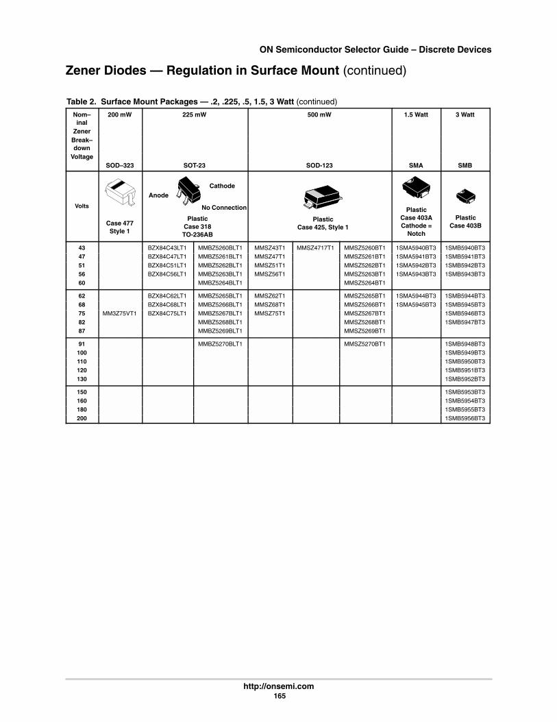
ON Semiconductor Selector Guide – Discrete Devices
http://onsemi.com 165
Zener Diodes — Regulation in Surface Mount (continued)
Table 2. Surface Mount Packages — .2, .225, .5, 1.5, 3 Watt (continued)
Nom–inal
200 mW 225 mW 500 mW 1.5 Watt 3 Watt
ZenerBreak–down
VoltageSOD–323 SOT-23 SOD-123 SMA SMB
Volts
Case 477Style 1
PlasticCase 318TO-236AB
AnodeCathode
No Connection
PlasticCase 425, Style 1
PlasticCase 403ACathode =
Notch
PlasticCase 403B
ÁÁÁÁÁÁÁÁ
43 ÁÁÁÁÁÁÁÁ
ÁÁÁÁÁÁÁÁ
BZX84C43LT1ÁÁÁÁÁÁÁÁÁÁ
MMBZ5260BLT1ÁÁÁÁÁÁÁÁ
MMSZ43T1ÁÁÁÁÁÁÁÁÁÁ
MMSZ4717T1ÁÁÁÁÁÁÁÁ
MMSZ5260BT1ÁÁÁÁÁÁÁÁÁÁ
1SMA5940BT3ÁÁÁÁÁÁÁÁ
1SMB5940BT3
ÁÁÁÁ47 ÁÁÁÁÁÁÁÁBZX84C47LT1ÁÁÁÁÁMMBZ5261BLT1ÁÁÁÁMMSZ47T1ÁÁÁÁÁÁÁÁÁMMSZ5261BT1ÁÁÁÁÁ1SMA5941BT3ÁÁÁÁ1SMB5941BT3ÁÁÁÁÁÁÁÁ
51 ÁÁÁÁÁÁÁÁ
ÁÁÁÁÁÁÁÁ
BZX84C51LT1ÁÁÁÁÁÁÁÁÁÁ
MMBZ5262BLT1ÁÁÁÁÁÁÁÁ
MMSZ51T1ÁÁÁÁÁÁÁÁÁÁ
ÁÁÁÁÁÁÁÁ
MMSZ5262BT1ÁÁÁÁÁÁÁÁÁÁ
1SMA5942BT3ÁÁÁÁÁÁÁÁ
1SMB5942BT3
ÁÁÁÁÁÁÁÁ
56 ÁÁÁÁÁÁÁÁ
ÁÁÁÁÁÁÁÁ
BZX84C56LT1ÁÁÁÁÁÁÁÁÁÁ
MMBZ5263BLT1ÁÁÁÁÁÁÁÁ
MMSZ56T1ÁÁÁÁÁÁÁÁÁÁ
ÁÁÁÁÁÁÁÁ
MMSZ5263BT1ÁÁÁÁÁÁÁÁÁÁ
1SMA5943BT3ÁÁÁÁÁÁÁÁ
1SMB5943BT3
ÁÁÁÁ60ÁÁÁÁÁÁÁÁÁÁÁÁÁ
MMBZ5264BLT1
ÁÁÁÁÁÁÁÁÁÁÁÁÁMMSZ5264BT1
ÁÁÁÁÁÁÁÁÁÁÁÁÁÁÁÁÁ
62ÁÁÁÁÁÁÁÁ
ÁÁÁÁÁÁÁÁ
BZX84C62LT1ÁÁÁÁÁÁÁÁÁÁ
MMBZ5265BLT1ÁÁÁÁÁÁÁÁ
MMSZ62T1ÁÁÁÁÁÁÁÁÁÁ
ÁÁÁÁÁÁÁÁ
MMSZ5265BT1ÁÁÁÁÁÁÁÁÁÁ
1SMA5944BT3ÁÁÁÁÁÁÁÁ
1SMB5944BT3
ÁÁÁÁÁÁÁÁ
68 ÁÁÁÁÁÁÁÁ
ÁÁÁÁÁÁÁÁ
BZX84C68LT1ÁÁÁÁÁÁÁÁÁÁ
MMBZ5266BLT1ÁÁÁÁÁÁÁÁ
MMSZ68T1ÁÁÁÁÁÁÁÁÁÁ
ÁÁÁÁÁÁÁÁ
MMSZ5266BT1ÁÁÁÁÁÁÁÁÁÁ
1SMA5945BT3ÁÁÁÁÁÁÁÁ
1SMB5945BT3
ÁÁÁÁ75 ÁÁÁÁMM3Z75VT1ÁÁÁÁBZX84C75LT1ÁÁÁÁÁMMBZ5267BLT1ÁÁÁÁMMSZ75T1ÁÁÁÁÁÁÁÁÁMMSZ5267BT1ÁÁÁÁÁÁÁÁÁ1SMB5946BT3ÁÁÁÁÁÁÁÁ
82 ÁÁÁÁÁÁÁÁ
ÁÁÁÁÁÁÁÁ
ÁÁÁÁÁÁÁÁÁÁ
MMBZ5268BLT1ÁÁÁÁÁÁÁÁ
ÁÁÁÁÁÁÁÁÁÁ
ÁÁÁÁÁÁÁÁ
MMSZ5268BT1ÁÁÁÁÁÁÁÁÁÁ
ÁÁÁÁÁÁÁÁ
1SMB5947BT3
ÁÁÁÁÁÁÁÁ
87 ÁÁÁÁÁÁÁÁ
ÁÁÁÁÁÁÁÁ
ÁÁÁÁÁÁÁÁÁÁ
MMBZ5269BLT1ÁÁÁÁÁÁÁÁ
ÁÁÁÁÁÁÁÁÁÁ
ÁÁÁÁÁÁÁÁ
MMSZ5269BT1ÁÁÁÁÁÁÁÁÁÁ
ÁÁÁÁÁÁÁÁÁÁÁÁ91 ÁÁÁÁÁÁÁÁÁÁÁÁÁMMBZ5270BLT1ÁÁÁÁÁÁÁÁÁÁÁÁÁMMSZ5270BT1ÁÁÁÁÁÁÁÁÁ1SMB5948BT3ÁÁÁÁ
ÁÁÁÁ100ÁÁÁÁÁÁÁÁ
ÁÁÁÁÁÁÁÁ
ÁÁÁÁÁÁÁÁÁÁ
ÁÁÁÁÁÁÁÁ
ÁÁÁÁÁÁÁÁÁÁ
ÁÁÁÁÁÁÁÁ
ÁÁÁÁÁÁÁÁÁÁ
ÁÁÁÁÁÁÁÁ
1SMB5949BT3
ÁÁÁÁÁÁÁÁ
110 ÁÁÁÁÁÁÁÁ
ÁÁÁÁÁÁÁÁ
ÁÁÁÁÁÁÁÁÁÁ
ÁÁÁÁÁÁÁÁ
ÁÁÁÁÁÁÁÁÁÁ
ÁÁÁÁÁÁÁÁ
ÁÁÁÁÁÁÁÁÁÁ
ÁÁÁÁÁÁÁÁ
1SMB5950BT3
ÁÁÁÁ120 ÁÁÁÁÁÁÁÁÁÁÁÁÁÁÁÁÁÁÁÁÁÁÁÁÁÁÁÁÁÁÁÁÁÁÁ1SMB5951BT3ÁÁÁÁÁÁÁÁ
130 ÁÁÁÁÁÁÁÁ
ÁÁÁÁÁÁÁÁ
ÁÁÁÁÁÁÁÁÁÁ
ÁÁÁÁÁÁÁÁ
ÁÁÁÁÁÁÁÁÁÁ
ÁÁÁÁÁÁÁÁ
ÁÁÁÁÁÁÁÁÁÁ
ÁÁÁÁÁÁÁÁ
1SMB5952BT3
ÁÁÁÁÁÁÁÁ
150 ÁÁÁÁÁÁÁÁ
ÁÁÁÁÁÁÁÁ
ÁÁÁÁÁÁÁÁÁÁ
ÁÁÁÁÁÁÁÁ
ÁÁÁÁÁÁÁÁÁÁ
ÁÁÁÁÁÁÁÁ
ÁÁÁÁÁÁÁÁÁÁ
ÁÁÁÁÁÁÁÁ
1SMB5953BT3
ÁÁÁÁÁÁÁÁ
160 ÁÁÁÁÁÁÁÁ
ÁÁÁÁÁÁÁÁ
ÁÁÁÁÁÁÁÁÁÁ
ÁÁÁÁÁÁÁÁ
ÁÁÁÁÁÁÁÁÁÁ
ÁÁÁÁÁÁÁÁ
ÁÁÁÁÁÁÁÁÁÁ
ÁÁÁÁÁÁÁÁ
1SMB5954BT3
ÁÁÁÁ180ÁÁÁÁÁÁÁÁÁÁÁÁÁÁÁÁÁÁÁÁÁÁÁÁÁÁÁÁÁÁÁÁÁÁÁ
1SMB5955BT3ÁÁÁÁÁÁÁÁ
200 ÁÁÁÁÁÁÁÁ
ÁÁÁÁÁÁÁÁ
ÁÁÁÁÁÁÁÁÁÁ
ÁÁÁÁÁÁÁÁ
ÁÁÁÁÁÁÁÁÁÁ
ÁÁÁÁÁÁÁÁ
ÁÁÁÁÁÁÁÁÁÁ
ÁÁÁÁÁÁÁÁ
1SMB5956BT3
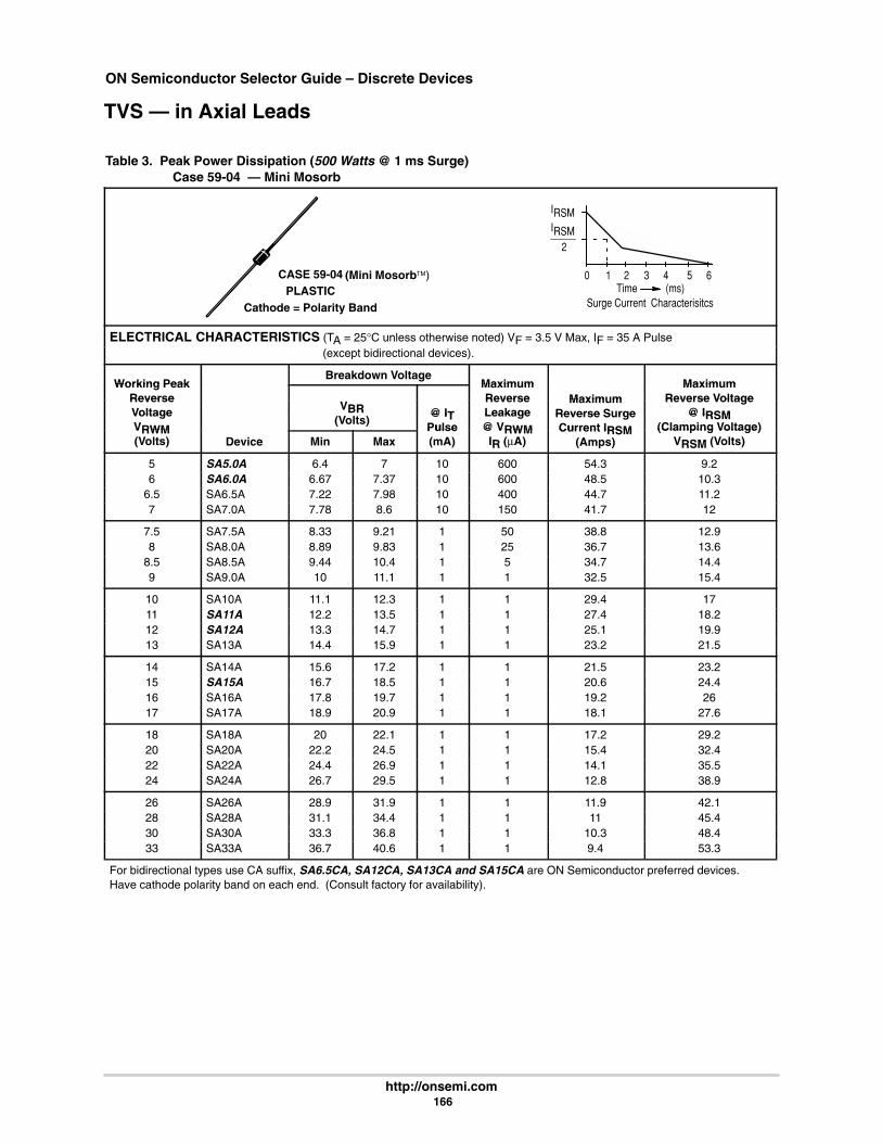
ON Semiconductor Selector Guide – Discrete Devices
http://onsemi.com 166
TVS — in Axial Leads
Table 3. Peak Power Dissipation (500 Watts @ 1 ms Surge)Case 59-04 — Mini Mosorb
CASE 59-04PLASTIC
Cathode = Polarity Band
0 1 2 3 4 5 6
IRSM
IRSM
Time (ms)Surge Current Characterisitcs
2
(Mini Mosorb)
ELECTRICAL CHARACTERISTICS (TA = 25°C unless otherwise noted) VF = 3.5 V Max, IF = 35 A Pulse(except bidirectional devices).
Working PeakBreakdown Voltage
Maxim m Maxim mWorking PeakReverse
MaximumReverse Maxim m
MaximumReverse VoltageReverse
Voltage VBR @ IT
ReverseLeakage
MaximumReverse S rge
Reverse Voltage@ IRSMVoltage
VRWM(Volts)
@ ITPulse
Leakage@ VRWM
Reverse SurgeCurrent IRSM
@ IRSM(Clamping Voltage)VRWM
(Volts) Device Min MaxPulse(mA)
@ VRWMIR (µA)
Current IRSM(Amps)
(Clamping Voltage)VRSM (Volts)
5 SA5.0A 6.4 7 10 600 54.3 9.26 SA6.0A 6.67 7.37 10 600 48.5 10.3
6.5 SA6.5A 7.22 7.98 10 400 44.7 11.27 SA7.0A 7.78 8.6 10 150 41.7 12
7.5 SA7.5A 8.33 9.21 1 50 38.8 12.98 SA8.0A 8.89 9.83 1 25 36.7 13.6
8.5 SA8.5A 9.44 10.4 1 5 34.7 14.49 SA9.0A 10 11.1 1 1 32.5 15.4
10 SA10A 11.1 12.3 1 1 29.4 1711 SA11A 12.2 13.5 1 1 27.4 18.212 SA12A 13.3 14.7 1 1 25.1 19.913 SA13A 14.4 15.9 1 1 23.2 21.5
14 SA14A 15.6 17.2 1 1 21.5 23.215 SA15A 16.7 18.5 1 1 20.6 24.416 SA16A 17.8 19.7 1 1 19.2 2617 SA17A 18.9 20.9 1 1 18.1 27.6
18 SA18A 20 22.1 1 1 17.2 29.220 SA20A 22.2 24.5 1 1 15.4 32.422 SA22A 24.4 26.9 1 1 14.1 35.524 SA24A 26.7 29.5 1 1 12.8 38.9
26 SA26A 28.9 31.9 1 1 11.9 42.128 SA28A 31.1 34.4 1 1 11 45.430 SA30A 33.3 36.8 1 1 10.3 48.433 SA33A 36.7 40.6 1 1 9.4 53.3
For bidirectional types use CA suffix, SA6.5CA, SA12CA, SA13CA and SA15CA are ON Semiconductor preferred devices.Have cathode polarity band on each end. (Consult factory for availability).
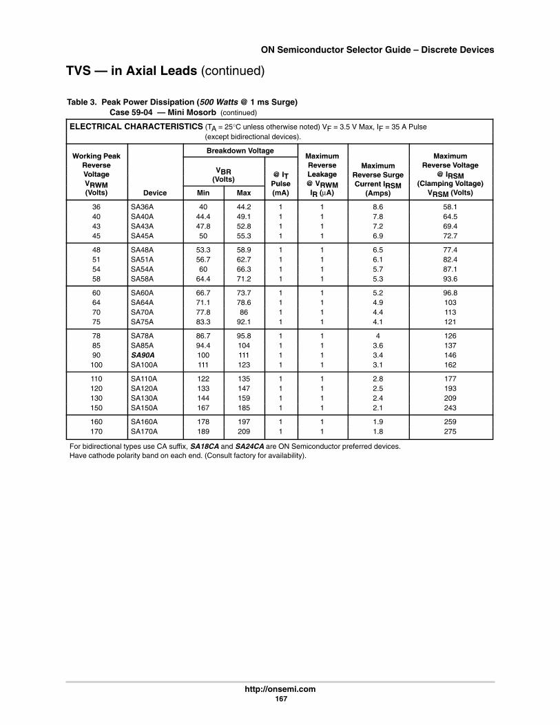
ON Semiconductor Selector Guide – Discrete Devices
http://onsemi.com 167
TVS — in Axial Leads (continued)
Table 3. Peak Power Dissipation (500 Watts @ 1 ms Surge)Case 59-04 — Mini Mosorb (continued)
ELECTRICAL CHARACTERISTICS (TA = 25°C unless otherwise noted) VF = 3.5 V Max, IF = 35 A Pulse(except bidirectional devices).
Working PeakBreakdown Voltage
Maxim m Maxim mWorking PeakReverse
MaximumReverse Maxim m
MaximumReverse VoltageReverse
Voltage VBR @ IT
ReverseLeakage
MaximumReverse S rge
Reverse Voltage@ IRSMVoltage
VRWM(Volts)
@ ITPulse
Leakage@ VRWM
Reverse SurgeCurrent IRSM
@ IRSM(Clamping Voltage)VRWM
(Volts) Device Min MaxPulse(mA)
@ VRWMIR (µA)
Current IRSM(Amps)
(Clamping Voltage)VRSM (Volts)
36 SA36A 40 44.2 1 1 8.6 58.140 SA40A 44.4 49.1 1 1 7.8 64.543 SA43A 47.8 52.8 1 1 7.2 69.445 SA45A 50 55.3 1 1 6.9 72.7
48 SA48A 53.3 58.9 1 1 6.5 77.451 SA51A 56.7 62.7 1 1 6.1 82.454 SA54A 60 66.3 1 1 5.7 87.158 SA58A 64.4 71.2 1 1 5.3 93.6
60 SA60A 66.7 73.7 1 1 5.2 96.864 SA64A 71.1 78.6 1 1 4.9 10370 SA70A 77.8 86 1 1 4.4 11375 SA75A 83.3 92.1 1 1 4.1 121
78 SA78A 86.7 95.8 1 1 4 12685 SA85A 94.4 104 1 1 3.6 13790 SA90A 100 111 1 1 3.4 146100 SA100A 111 123 1 1 3.1 162
110 SA110A 122 135 1 1 2.8 177120 SA120A 133 147 1 1 2.5 193130 SA130A 144 159 1 1 2.4 209150 SA150A 167 185 1 1 2.1 243
160 SA160A 178 197 1 1 1.9 259170 SA170A 189 209 1 1 1.8 275
For bidirectional types use CA suffix, SA18CA and SA24CA are ON Semiconductor preferred devices.Have cathode polarity band on each end. (Consult factory for availability).

ON Semiconductor Selector Guide – Discrete Devices
http://onsemi.com 168
TVS — in Axial Leads (continued)
Table 4. Peak Power Dissipation (600 Watts @ 1 ms Surge)Case 17 — Surmetic 40
CASE 17PLASTIC
Cathode = Polarity Band
0 1 2 3 4 5 6
IRSM
IRSM
Time (ms)Surge Current Characterisitcs
2
ELECTRICAL CHARACTERISTICS (TA = 25°C unless otherwise noted) VF = 3.5 V Max, IF = 50 A Pulse(except bidirectional devices).
BreakdownVoltage Working Peak Maximum Maximum
VBR @ IT
ReverseVoltage
ReverseLeakage
MaximumReverse S rge
Reverse Voltage@ IRSM(Volts) @ IT
P lseVoltageVRWM
Leakage@ VRWM
Reverse SurgeC rrent IRSM
@ IRSM(Clamping Voltage)
NomPulse(mA) Device
VRWM(Volts)
@ VRWMIR (µA)
Current IRSM(Amps)
(Clamping Voltage)VRSM (Volts)Nom (mA) Device (Volts) IR (µA) (Amps) VRSM (Volts)
6.8 10 P6KE6.8A 5.8 1000 57 10.57.5 10 P6KE7.5A 6.4 500 53 11.38.2 10 P6KE8.2A 7.02 200 50 12.19.1 1 P6KE9.1A 7.78 50 45 13.4
10 1 P6KE10A 8.55 10 41 14.511 1 P6KE11A 9.4 5 38 15.612 1 P6KE12A 10.2 5 36 16.713 1 P6KE13A 11.1 5 33 18.2
15 1 P6KE15A 12.8 5 28 21.216 1 P6KE16A 13.6 5 27 22.518 1 P6KE18A 15.3 5 24 25.220 1 P6KE20A 17.1 5 22 27.7
22 1 P6KE22A 18.8 5 20 30.624 1 P6KE24A 20.5 5 18 33.227 1 P6KE27A 23.1 5 16 37.530 1 P6KE30A 25.6 5 14.4 41.4
33 1 P6KE33A 28.2 5 13.2 45.736 1 P6KE36A 30.8 5 12 49.939 1 P6KE39A 33.3 5 11.2 53.943 1 P6KE43A 36.8 5 10.1 59.3
47 1 P6KE47A 40.2 5 9.3 64.851 1 P6KE51A 43.6 5 8.6 70.156 1 P6KE56A 47.8 5 7.8 7762 1 P6KE62A 53 5 7.1 85
68 1 P6KE68A 58.1 5 6.5 9275 1 P6KE75A 64.1 5 5.8 10382 1 P6KE82A 70.1 5 5.3 11391 1 P6KE91A 77.8 5 4.8 125
100 1 P6KE100A 85.5 5 4.4 137110 1 P6KE110A 94 5 4 152120 1 P6KE120A 102 5 3.6 165130 1 P6KE130A 111 5 3.3 179
For bidirectional types use CA suffix, P6KE7.5CA and P6KE11CA are ON Semiconductor preferred devices.

ON Semiconductor Selector Guide – Discrete Devices
http://onsemi.com 169
TVS — in Axial Leads (continued)
Table 4. Peak Power Dissipation (600 Watts @ 1 ms Surge)Case 17 — Surmetic 40 (continued)
ELECTRICAL CHARACTERISTICS (TA = 25°C unless otherwise noted) VF = 3.5 V Max, IF = 50 A Pulse(except bidirectional devices).
BreakdownVoltage Working Peak Maximum Maximum
VBR @ IT
ReverseVoltage
ReverseLeakage
MaximumReverse S rge
Reverse Voltage@ IRSM(Volts) @ IT
P lseVoltageVRWM
Leakage@ VRWM
Reverse SurgeC rrent IRSM
@ IRSM(Clamping Voltage)
NomPulse(mA) Device
VRWM(Volts)
@ VRWMIR (µA)
Current IRSM(Amps)
(Clamping Voltage)VRSM (Volts)Nom (mA) Device (Volts) IR (µA) (Amps) VRSM (Volts)
150 1 P6KE150A 128 5 2.9 207160 1 P6KE160A 136 5 2.7 219170 1 P6KE170A 145 5 2.6 234180 1 P6KE180A 154 5 2.4 246200 1 P6KE200A 171 5 2.2 274
For bidirectional types use CA suffix. Have cathode polarity band on each end. (Consult factory for availability).
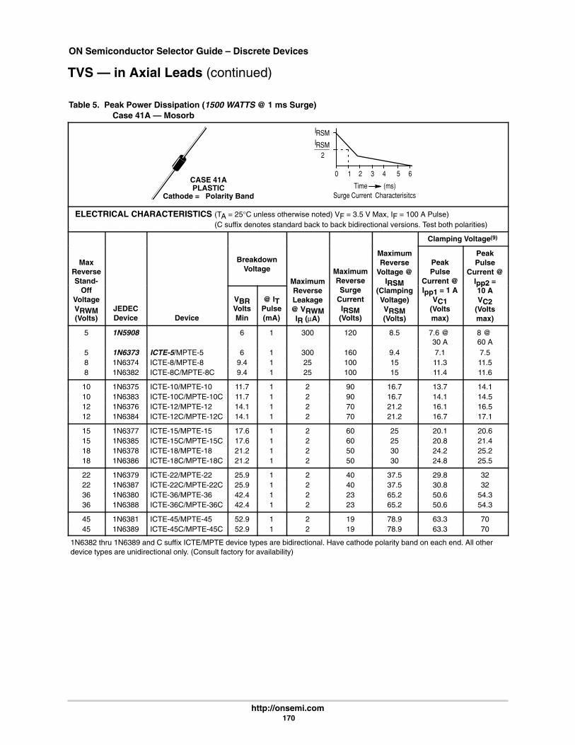
ON Semiconductor Selector Guide – Discrete Devices
http://onsemi.com 170
TVS — in Axial Leads (continued)
Table 5. Peak Power Dissipation (1500 WATTS @ 1 ms Surge)Case 41A — Mosorb
CASE 41APLASTIC
Cathode = Polarity Band
0 1 2 3 4 5 6
IRSM
IRSM
Time (ms)Surge Current Characterisitcs
2
ELECTRICAL CHARACTERISTICS (TA = 25°C unless otherwise noted) VF = 3.5 V Max, IF = 100 A Pulse)ELECTRICAL CHARACTERISTICS (C suffix denotes standard back to back bidirectional versions. Test both polarities)
Clamping Voltage(9)
MaxReverseStand-
BreakdownVoltage
MaximumMaximumReverse
MaximumReverse
Voltage @IRSM
PeakPulse
Current @
PeakPulse
Current @Ipp2 =
OffVoltageVRWM(Volts)
JEDECDevice Device
VBRVoltsMin
@ ITPulse(mA)
ReverseLeakage@ VRWM
IR (µA)
SurgeCurrentIRSM(Volts)
RSM(ClampingVoltage)VRSM(Volts)
Ipp1 = 1 AVC1
(Voltsmax)
pp210 AVC2
(Voltsmax)
5 1N5908 6 1 300 120 8.5 7.6 @30 A
8 @60 A
5 1N6373 ICTE-5/MPTE-5 6 1 300 160 9.4 7.1 7.58 1N6374 ICTE-8/MPTE-8 9.4 1 25 100 15 11.3 11.58 1N6382 ICTE-8C/MPTE-8C 9.4 1 25 100 15 11.4 11.6
10 1N6375 ICTE-10/MPTE-10 11.7 1 2 90 16.7 13.7 14.110 1N6383 ICTE-10C/MPTE-10C 11.7 1 2 90 16.7 14.1 14.512 1N6376 ICTE-12/MPTE-12 14.1 1 2 70 21.2 16.1 16.512 1N6384 ICTE-12C/MPTE-12C 14.1 1 2 70 21.2 16.7 17.1
15 1N6377 ICTE-15/MPTE-15 17.6 1 2 60 25 20.1 20.615 1N6385 ICTE-15C/MPTE-15C 17.6 1 2 60 25 20.8 21.418 1N6378 ICTE-18/MPTE-18 21.2 1 2 50 30 24.2 25.218 1N6386 ICTE-18C/MPTE-18C 21.2 1 2 50 30 24.8 25.5
22 1N6379 ICTE-22/MPTE-22 25.9 1 2 40 37.5 29.8 3222 1N6387 ICTE-22C/MPTE-22C 25.9 1 2 40 37.5 30.8 3236 1N6380 ICTE-36/MPTE-36 42.4 1 2 23 65.2 50.6 54.336 1N6388 ICTE-36C/MPTE-36C 42.4 1 2 23 65.2 50.6 54.3
45 1N6381 ICTE-45/MPTE-45 52.9 1 2 19 78.9 63.3 7045 1N6389 ICTE-45C/MPTE-45C 52.9 1 2 19 78.9 63.3 70
1N6382 thru 1N6389 and C suffix ICTE/MPTE device types are bidirectional. Have cathode polarity band on each end. All otherdevice types are unidirectional only. (Consult factory for availability)
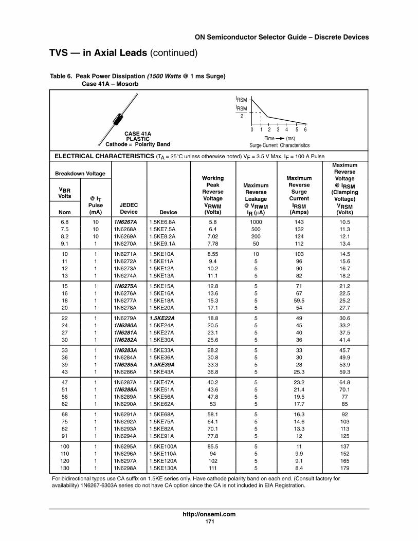
ON Semiconductor Selector Guide – Discrete Devices
http://onsemi.com 171
TVS — in Axial Leads (continued)
Table 6. Peak Power Dissipation (1500 Watts @ 1 ms Surge)Case 41A – Mosorb
0 1 2 3 4 5 6
IRSM
IRSM
Time (ms)Surge Current Characterisitcs
2
CASE 41APLASTIC
Cathode = Polarity Band
ELECTRICAL CHARACTERISTICS (TA = 25°C unless otherwise noted) VF = 3.5 V Max, IF = 100 A Pulse
Breakdown VoltageWorking Maxim m
MaximumReverseVoltage
VBRVolts @ IT
WorkingPeak
ReverseVoltage
MaximumReverseLeakage
MaximumReverseSurge
Current
Voltage@ IRSM
(ClampingVoltage)
Nom
@ ITPulse(mA)
JEDECDevice Device
VoltageVRWM(Volts)
Leakage@ VRWM
IR (µA)
CurrentIRSM
(Amps)
Voltage)VRSM(Volts)
6.8 10 1N6267A 1.5KE6.8A 5.8 1000 143 10.57.5 10 1N6268A 1.5KE7.5A 6.4 500 132 11.38.2 10 1N6269A 1.5KE8.2A 7.02 200 124 12.19.1 1 1N6270A 1.5KE9.1A 7.78 50 112 13.4
10 1 1N6271A 1.5KE10A 8.55 10 103 14.511 1 1N6272A 1.5KE11A 9.4 5 96 15.612 1 1N6273A 1.5KE12A 10.2 5 90 16.713 1 1N6274A 1.5KE13A 11.1 5 82 18.2
15 1 1N6275A 1.5KE15A 12.8 5 71 21.216 1 1N6276A 1.5KE16A 13.6 5 67 22.518 1 1N6277A 1.5KE18A 15.3 5 59.5 25.220 1 1N6278A 1.5KE20A 17.1 5 54 27.7
22 1 1N6279A 1.5KE22A 18.8 5 49 30.624 1 1N6280A 1.5KE24A 20.5 5 45 33.227 1 1N6281A 1.5KE27A 23.1 5 40 37.530 1 1N6282A 1.5KE30A 25.6 5 36 41.4
33 1 1N6283A 1.5KE33A 28.2 5 33 45.736 1 1N6284A 1.5KE36A 30.8 5 30 49.939 1 1N6285A 1.5KE39A 33.3 5 28 53.943 1 1N6286A 1.5KE43A 36.8 5 25.3 59.3
47 1 1N6287A 1.5KE47A 40.2 5 23.2 64.851 1 1N6288A 1.5KE51A 43.6 5 21.4 70.156 1 1N6289A 1.5KE56A 47.8 5 19.5 7762 1 1N6290A 1.5KE62A 53 5 17.7 85
68 1 1N6291A 1.5KE68A 58.1 5 16.3 9275 1 1N6292A 1.5KE75A 64.1 5 14.6 10382 1 1N6293A 1.5KE82A 70.1 5 13.3 11391 1 1N6294A 1.5KE91A 77.8 5 12 125
100 1 1N6295A 1.5KE100A 85.5 5 11 137110 1 1N6296A 1.5KE110A 94 5 9.9 152120 1 1N6297A 1.5KE120A 102 5 9.1 165130 1 1N6298A 1.5KE130A 111 5 8.4 179
For bidirectional types use CA suffix on 1.5KE series only. Have cathode polarity band on each end. (Consult factory foravailability) 1N6267-6303A series do not have CA option since the CA is not included in EIA Registration.
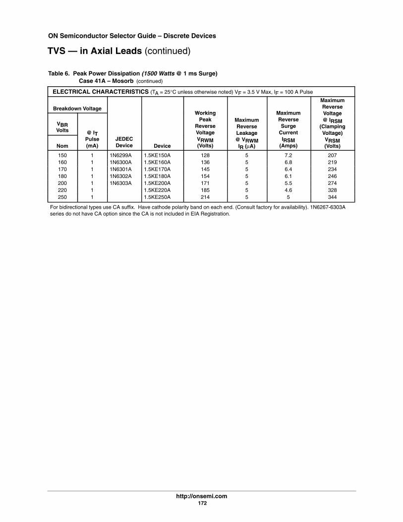
ON Semiconductor Selector Guide – Discrete Devices
http://onsemi.com 172
TVS — in Axial Leads (continued)
Table 6. Peak Power Dissipation (1500 Watts @ 1 ms Surge)Case 41A – Mosorb (continued)
ELECTRICAL CHARACTERISTICS (TA = 25°C unless otherwise noted) VF = 3.5 V Max, IF = 100 A Pulse
Breakdown VoltageWorking Maxim m
MaximumReverseVoltage
VBRVolts @ IT
WorkingPeak
ReverseVoltage
MaximumReverseLeakage
MaximumReverseSurge
Current
Voltage@ IRSM
(ClampingVoltage)
Nom
@ ITPulse(mA)
JEDECDevice Device
VoltageVRWM(Volts)
Leakage@ VRWM
IR (µA)
CurrentIRSM
(Amps)
Voltage)VRSM(Volts)
150 1 1N6299A 1.5KE150A 128 5 7.2 207160 1 1N6300A 1.5KE160A 136 5 6.8 219170 1 1N6301A 1.5KE170A 145 5 6.4 234180 1 1N6302A 1.5KE180A 154 5 6.1 246200 1 1N6303A 1.5KE200A 171 5 5.5 274220 1 1.5KE220A 185 5 4.6 328250 1 1.5KE250A 214 5 5 344
For bidirectional types use CA suffix. Have cathode polarity band on each end. (Consult factory for availability). 1N6267-6303Aseries do not have CA option since the CA is not included in EIA Registration.

ON Semiconductor Selector Guide – Discrete Devices
http://onsemi.com 173
TVS — in Surface Mount
Table 7. 1SMA Series Unidirectional Overvoltage Transient Suppressors; 400 Watts Peak Power
ELECTRICAL CHARACTERISTICS (VF = 3.5 Volts @ IF = 40 A for all types)
Reverse Breakdown Voltage MaximumReverse Voltage
MaximumReverse
Maximum
Device Stand–offVoltage VRWM
(Volts)
VBRVolts(Min)
ITmA
Reverse Voltage@ IRSM
(Clamping Volt-age) VRSM (Volts)
ReverseSurge Current
IRSM(Amps)
Reverse Leakage@ VRWM
IR (µA)
DevceMarking
SMACASE 403B–01
PLASTIC
1SMA5.0AT3 5.0 6.4 10 9.2 43.5 400 QE1SMA6.0AT3 6.0 6.67 10 10.3 38.8 400 QG1SMA6.5AT3 6.5 7.22 10 11.2 35.7 250 QK1SMA7.0AT3 7.0 7.78 10 12.0 33.3 250 QM
1SMA7.5AT3 7.5 8.33 1 12.9 31.0 50 QP1SMA8.0AT3 8.0 8.89 1 13.6 29.4 25 QR1SMA8.5AT3 8.5 9.44 1 14.4 27.8 5.0 QT1SMA9.0AT3 9.0 10 1 15.4 26.0 2.5 QV
1SMA10AT3 10 11.1 1 17.0 23.5 2.5 QX1SMA11AT3 11 12.2 1 18.2 22.0 2.5 QZ1SMA12AT3 12 13.3 1 19.9 20.1 2.5 RE1SMA13AT3 13 14.4 1 21.5 18.6 2.5 RG
1SMA14AT3 14 15.6 1 23.2 17.2 2.5 RK1SMA15AT3 15 16.7 1 24.4 16.4 2.5 RM1SMA16AT3 16 17.8 1 26.0 15.4 2.5 RP1SMA17AT3 17 18.9 1 27.6 14.5 2.5 RR
1SMA18AT3 18 20 1 29.2 13.7 2.5 RT1SMA20AT3 20 22.2 1 32.4 12.3 2.5 RV1SMA22AT3 22 24.4 1 35.5 11.3 2.5 RX1SMA24AT3 24 26.7 1 38.9 10.3 2.5 RZ
1SMA26AT3 26 28.9 1 42.1 9.5 2.5 SE1SMA28AT3 28 31.1 1 45.4 8.8 2.5 SG1SMA30AT3 30 33.3 1 48.4 8.3 2.5 SK1SMA33AT3 33 36.7 1 53.3 7.5 2.5 SM
1SMA36AT3 36 40 1 58.1 6.9 2.5 SP1SMA40AT3 40 44.4 1 64.5 6.2 2.5 SR1SMA43AT3 43 47.8 1 69.4 5.8 2.5 ST1SMA45AT3 45 50 1 72.2 5.5 2.5 SV
1SMA48AT3 48 53.3 1 77.4 5.2 2.5 SX1SMA51AT3 51 56.7 1 82.4 4.9 2.5 SZ1SMA54AT3 54 60 1 87.1 4.6 2.5 TE1SMA58AT3 58 64.4 1 93.6 4.8 2.5 TG
1SMA60AT3 60 66.7 1 96.8 4.1 2.5 TK1SMA64AT3 64 71.1 1 103.0 3.9 2.5 TM1SMA70AT3 70 77.8 1 113.0 3.5 2.5 TP1SMA75AT3 75 83.3 1 121.0 3.3 2.5 TR1SMA78AT3 78 86.7 1 126.0 3.2 2.5 TS

ON Semiconductor Selector Guide – Discrete Devices
http://onsemi.com 174
TVS — in Surface Mount (continued)
Table 8. 1SMA Series Bidirectional Zener Overvoltage Transient Suppressors; 400 Watts Peak Power
ELECTRICAL CHARACTERISTICS
ReverseBreakdown Voltage Maximum
Reverse VoltageMaximumReverse
Maximum
DeviceStand–off
Voltage VRWM(Volts)
VBRVolts(Min)
ITmA
g@ IRSM
(ClampingVoltage)
VRSM (Volts)
ReverseSurge Cur-rent IRSM
(Amps)
Reverse Leakage@ VRWM
IR (µA)
DevceMarking
SMACASE 403B–01
PLASTIC
1SMA10CAT3 10 11.1 1 17.0 23.5 2.5 QXC1SMA11CAT3 11 12.2 1 18.2 22.0 2.5 QZC1SMA12CAT3 12 13.3 1 19.9 20.1 2.5 REC1SMA13CAT3 13 14.4 1 21.5 18.6 2.5 RGC
1SMA14CAT3 14 15.6 1 23.2 17.2 2.5 RKC1SMA15CAT3 15 16.7 1 24.4 16.4 2.5 RMC1SMA16CAT3 16 17.8 1 26.0 15.4 2.5 RPC1SMA17CAT3 17 18.9 1 27.6 14.5 2.5 RRC
1SMA18CAT3 18 20 1 29.2 13.7 2.5 RTC1SMA20CAT3 20 22.2 1 32.4 12.3 2.5 RVC1SMA22CAT3 22 24.4 1 35.5 11.3 2.5 RXC1SMA24CAT3 24 26.7 1 38.9 10.3 2.5 RZC
1SMA26CAT3 26 28.9 1 42.1 9.5 2.5 SEC1SMA28CAT3 28 31.1 1 45.4 8.8 2.5 SGC1SMA30CAT3 30 33.3 1 48.4 8.3 2.5 SKC1SMA33CAT3 33 36.7 1 53.3 7.5 2.5 SMC
1SMA36CAT3 36 40 1 58.1 6.9 2.5 SPC1SMA40CAT3 40 44.4 1 64.5 6.2 2.5 SRC1SMA43CAT3 43 47.8 1 69.4 5.8 2.5 STC1SMA45CAT3 45 50 1 72.2 5.5 2.5 SVC
1SMA48CAT3 48 53.3 1 77.4 5.2 2.5 SXC1SMA51CAT3 51 56.7 1 82.4 4.9 2.5 SZC1SMA54CAT3 54 60 1 87.1 4.6 2.5 TEC1SMA58CAT3 58 64.4 1 93.6 4.3 2.5 TGC
1SMA60CAT3 60 66.7 1 96.8 4.1 2.5 TKC1SMA64CAT3 64 71.1 1 103.0 3.9 2.5 TMC1SMA70CAT3 70 77.8 1 113.0 3.5 2.5 TPC1SMA75CAT3 75 83.3 1 121.0 3.3 2.5 TRC1SMA78CAT3 78 86.7 1 126.0 3.2 2.5 TSC
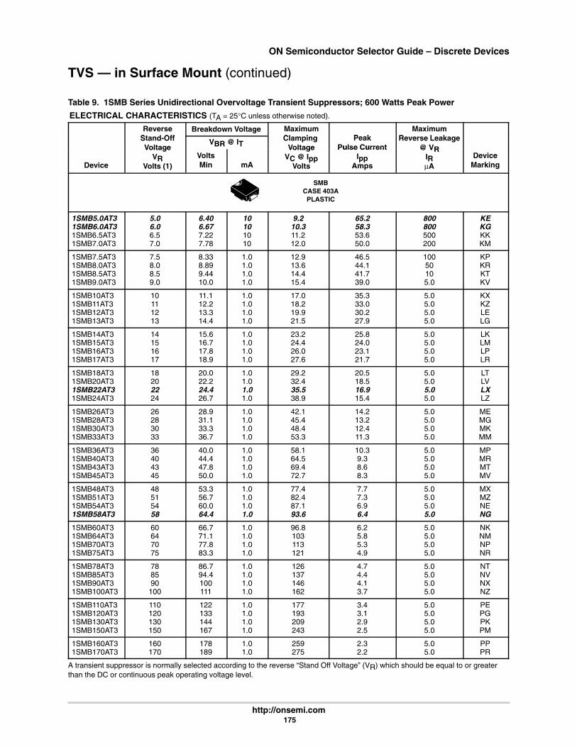
ON Semiconductor Selector Guide – Discrete Devices
http://onsemi.com 175
TVS — in Surface Mount (continued)
Table 9. 1SMB Series Unidirectional Overvoltage Transient Suppressors; 600 Watts Peak Power
ELECTRICAL CHARACTERISTICS (TA = 25°C unless otherwise noted).
ReverseSt d Off
Breakdown Voltage MaximumCl i P k
MaximumR L kStand-Off
VoltageVBR @ IT
Clamping Voltage
PeakPulse Current
Reverse Leakage@ VR
Device
VoltageVR
Volts (1)VoltsMin mA
VoltageVC @ Ipp
Volts
Pulse CurrentIpp
Amps
@ VRIRµA
DeviceMarking
SMBCASE 403A
PLASTIC
1SMB5.0AT31SMB6.0AT31SMB6.5AT31SMB7.0AT3
5.06.06.57.0
6.406.677.227.78
10101010
9.210.311.212.0
65.258.353.650.0
800800500200
KEKGKKKM
1SMB7.5AT31SMB8.0AT31SMB8.5AT31SMB9.0AT3
7.58.08.59.0
8.338.899.4410.0
1.01.01.01.0
12.913.614.415.4
46.544.141.739.0
10050105.0
KPKRKTKV
1SMB10AT31SMB11AT31SMB12AT31SMB13AT3
10111213
11.112.213.314.4
1.01.01.01.0
17.018.219.921.5
35.333.030.227.9
5.05.05.05.0
KXKZLELG
1SMB14AT31SMB15AT31SMB16AT31SMB17AT3
14151617
15.616.717.818.9
1.01.01.01.0
23.224.426.027.6
25.824.023.121.7
5.05.05.05.0
LKLMLPLR
1SMB18AT31SMB20AT31SMB22AT31SMB24AT3
18202224
20.022.224.426.7
1.01.01.01.0
29.232.435.538.9
20.518.516.915.4
5.05.05.05.0
LTLVLXLZ
1SMB26AT31SMB28AT31SMB30AT31SMB33AT3
26283033
28.931.133.336.7
1.01.01.01.0
42.145.448.453.3
14.213.212.411.3
5.05.05.05.0
MEMGMKMM
1SMB36AT31SMB40AT31SMB43AT31SMB45AT3
36404345
40.044.447.850.0
1.01.01.01.0
58.164.569.472.7
10.39.38.68.3
5.05.05.05.0
MPMRMTMV
1SMB48AT31SMB51AT31SMB54AT31SMB58AT3
48515458
53.356.760.064.4
1.01.01.01.0
77.482.487.193.6
7.77.36.96.4
5.05.05.05.0
MXMZNENG
1SMB60AT31SMB64AT31SMB70AT31SMB75AT3
60647075
66.771.177.883.3
1.01.01.01.0
96.8103113121
6.25.85.34.9
5.05.05.05.0
NKNMNPNR
1SMB78AT31SMB85AT31SMB90AT31SMB100AT3
788590100
86.794.4100111
1.01.01.01.0
126137146162
4.74.44.13.7
5.05.05.05.0
NTNVNXNZ
1SMB110AT31SMB120AT31SMB130AT31SMB150AT3
110120130150
122133144167
1.01.01.01.0
177193209243
3.43.12.92.5
5.05.05.05.0
PEPGPKPM
1SMB160AT31SMB170AT3
160170
178189
1.01.0
259275
2.32.2
5.05.0
PPPR
A transient suppressor is normally selected according to the reverse “Stand Off Voltage” (VR) which should be equal to or greaterthan the DC or continuous peak operating voltage level.
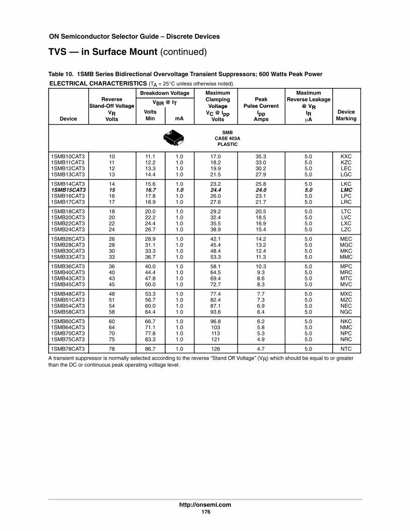
ON Semiconductor Selector Guide – Discrete Devices
http://onsemi.com 176
TVS — in Surface Mount (continued)
Table 10. 1SMB Series Bidirectional Overvoltage Transient Suppressors; 600 Watts Peak Power
ELECTRICAL CHARACTERISTICS (TA = 25°C unless otherwise noted).
RBreakdown Voltage Maximum
Cl i P kMaximum
R L kReverseStand-Off Voltage
VBR @ ITClampingVoltage
PeakPulse Current
Reverse Leakage@ VR
Device
Stand Off VoltageVR
VoltsVoltsMin mA
VoltageVC @ Ipp
Volts
Pulse CurrentIpp
Amps
@ VRIRµA
DeviceMarking
SMBCASE 403A
PLASTIC
1SMB10CAT31SMB11CAT31SMB12CAT31SMB13CAT3
10111213
11.112.213.314.4
1.01.01.01.0
17.018.219.921.5
35.333.030.227.9
5.05.05.05.0
KXCKZCLECLGC
1SMB14CAT31SMB15CAT31SMB16CAT31SMB17CAT3
14151617
15.616.717.818.9
1.01.01.01.0
23.224.426.027.6
25.824.023.121.7
5.05.05.05.0
LKCLMCLPCLRC
1SMB18CAT31SMB20CAT31SMB22CAT31SMB24CAT3
18202224
20.022.224.426.7
1.01.01.01.0
29.232.435.538.9
20.518.516.915.4
5.05.05.05.0
LTCLVCLXCLZC
1SMB26CAT31SMB28CAT31SMB30CAT31SMB33CAT3
26283033
28.931.133.336.7
1.01.01.01.0
42.145.448.453.3
14.213.212.411.3
5.05.05.05.0
MECMGCMKCMMC
1SMB36CAT31SMB40CAT31SMB43CAT31SMB45CAT3
36404345
40.044.447.850.0
1.01.01.01.0
58.164.569.472.7
10.39.38.68.3
5.05.05.05.0
MPCMRCMTCMVC
1SMB48CAT31SMB51CAT31SMB54CAT31SMB58CAT3
48515458
53.356.760.064.4
1.01.01.01.0
77.482.487.193.6
7.77.36.96.4
5.05.05.05.0
MXCMZCNECNGC
1SMB60CAT31SMB64CAT31SMB70CAT31SMB75CAT3
60647075
66.771.177.883.3
1.01.01.01.0
96.8103113121
6.25.85.34.9
5.05.05.05.0
NKCNMCNPCNRC
1SMB78CAT3 78 86.7 1.0 126 4.7 5.0 NTC
A transient suppressor is normally selected according to the reverse “Stand Off Voltage” (VR) which should be equal to or greaterthan the DC or continuous peak operating voltage level.

ON Semiconductor Selector Guide – Discrete Devices
http://onsemi.com 177
TVS — in Surface Mount (continued)
Table 11. P6SMB Series Unidirectional Overvoltage Transient Suppressors; 600 Watts Peak Power
ELECTRICAL CHARACTERISTICS (TA = 25°C unless otherwise noted) VF = 3.5 V Max, IF = 50 A for all types.
Breakdown Voltage Working Maximum Maximum
MaximumReverseVoltage
VBR @ ITVolts
gPeak
ReverseVoltage
ReverseLeakage@ VRWM
ReverseSurge
Current
g@ IRSM
(ClampingVoltage)
MaximumTemperatureCoefficient
Device Min Nom Max mAVRWMVolts
IRµA
IRSMAmps
VRSMVolts
of VBR%/°C
DeviceMarking
SMBCASE 403A
PLASTIC
P6SMB6.8AT3P6SMB7.5AT3P6SMB8.2AT3P6SMB9.1AT3
6.457.137.798.65
6.87.58.29.1
7.147.888.619.55
1010101
5.86.47.027.78
100050020050
57535045
10.511.312.113.4
0.0570.0610.0650.068
6V8A7V5A8V2A9V1A
P6SMB10AT3P6SMB11AT3P6SMB12AT3P6SMB13AT3
9.510.511.412.4
10111213
10.511.612.613.7
1111
8.559.410.211.1
10555
41383633
14.515.616.718.2
0.0730.0750.0780.081
10A11A12A13A
P6SMB15AT3P6SMB16AT3P6SMB18AT3P6SMB20AT3
14.315.217.119
15161820
15.816.818.921
1111
12.813.615.317.1
5555
28272422
21.222.525.227.7
0.0840.0860.0880.09
15A16A18A20A
P6SMB22AT3P6SMB24AT3P6SMB27AT3P6SMB30AT3
20.922.825.728.5
22242730
23.125.228.431.5
1111
18.820.523.125.6
5555
201816
14.4
30.633.237.541.4
0.0920.0940.0960.097
22A24A27A30A
P6SMB33AT3P6SMB36AT3P6SMB39AT3P6SMB43AT3
31.434.237.140.9
33363943
34.737.841
45.2
1111
28.230.833.336.8
5555
13.212
11.210.1
45.749.953.959.3
0.0980.0990.1
0.101
33A36A39A43A
P6SMB47AT3P6SMB51AT3P6SMB56AT3P6SMB62AT3
44.748.553.258.9
47515662
49.453.658.865.1
1111
40.243.647.853
5555
9.38.67.87.1
64.870.17785
0.1010.1020.1030.104
47A51A56A62A
P6SMB68AT3P6SMB75AT3P6SMB82AT3P6SMB91AT3
64.671.377.986.5
68758291
71.478.886.195.5
1111
58.164.170.177.8
5555
6.55.85.34.8
92103113125
0.1040.1050.1050.106
68A75A82A91A
P6SMB100AT3P6SMB110AT3P6SMB120AT3P6SMB130AT3
95105114124
100110120130
105116126137
1111
85.594102111
5555
4.44
3.63.3
137152165179
0.1060.1070.1070.107
100A110A120A130A
P6SMB150AT3P6SMB160AT3P6SMB170AT3P6SMB180AT3
143152162171
150160170180
158168179189
1111
128136145154
5555
2.92.72.62.4
207219234246
0.1080.1080.1080.108
150A160A170A180A
P6SMB200AT3 190 200 210 1 171 5 2.2 274 0.108 200A

ON Semiconductor Selector Guide – Discrete Devices
http://onsemi.com 178
TVS — in Surface Mount (continued)
Table 12. P6SMB Series Bidirectional Overvoltage Transient Suppressors; 600 Watts Peak Power
ELECTRICAL CHARACTERISTICS (TA = 25°C unless otherwise noted) VF = 3.5 V Max, IF = 50 A for all types.
Breakdown Voltage Working Maximum Maximum
MaximumReverseVoltage
VBR @ ITVolts
gPeak
ReverseVoltage
ReverseLeakage@ VRWM
ReverseSurge
Current
g@ IRSM
(ClampingVoltage)
MaximumTemperatureCoefficient
Device Min Nom Max mAVRWMVolts
IRµA
IRSMAmps
VRSMVolts
of VBR%/°C
DeviceMarking
SMBCASE 403A
PLASTIC
P6SMB11CAT3P6SMB12CAT3P6SMB13CAT3
10.511.412.4
111213
11.612.613.7
111
9.410.211.1
555
383633
15.616.718.2
0.0750.0780.081
11C12C13C
P6SMB15CAT3P6SMB16CAT3P6SMB18CAT3P6SMB20CAT3
14.315.217.119
15161820
15.816.818.921
1111
12.813.615.317.1
5555
28272422
21.222.525.227.7
0.0840.0860.0880.09
15C16C18C20C
P6SMB22CAT3P6SMB24CAT3P6SMB27CAT3P6SMB30CAT3
20.922.825.728.5
22242730
23.125.228.431.5
1111
18.820.523.125.6
5555
201816
14.4
30.633.237.541.4
0.0920.0940.0960.097
22C24C27C30C
P6SMB33CAT3P6SMB36CAT3P6SMB39CAT3P6SMB43CAT3
31.434.237.140.9
33363943
34.737.841
45.2
1111
28.230.833.336.8
5555
13.212
11.210.1
45.749.953.959.3
0.0980.0990.1
0.101
33C36C39C43C
P6SMB47CAT3P6SMB51CAT3P6SMB56CAT3P6SMB62CAT3
44.748.553.258.9
47515662
49.453.658.865.1
1111
40.243.647.853
5555
9.38.67.87.1
64.870.17785
0.1010.1020.1030.104
47C51C56C62C
P6SMB68CAT3P6SMB75CAT3P6SMB82CAT3P6SMB91CAT3
64.671.377.986.5
68758291
71.478.886.195.5
1111
58.164.170.177.8
5555
6.55.85.34.8
92103113125
0.1040.1050.1050.106
68C75C82C91C
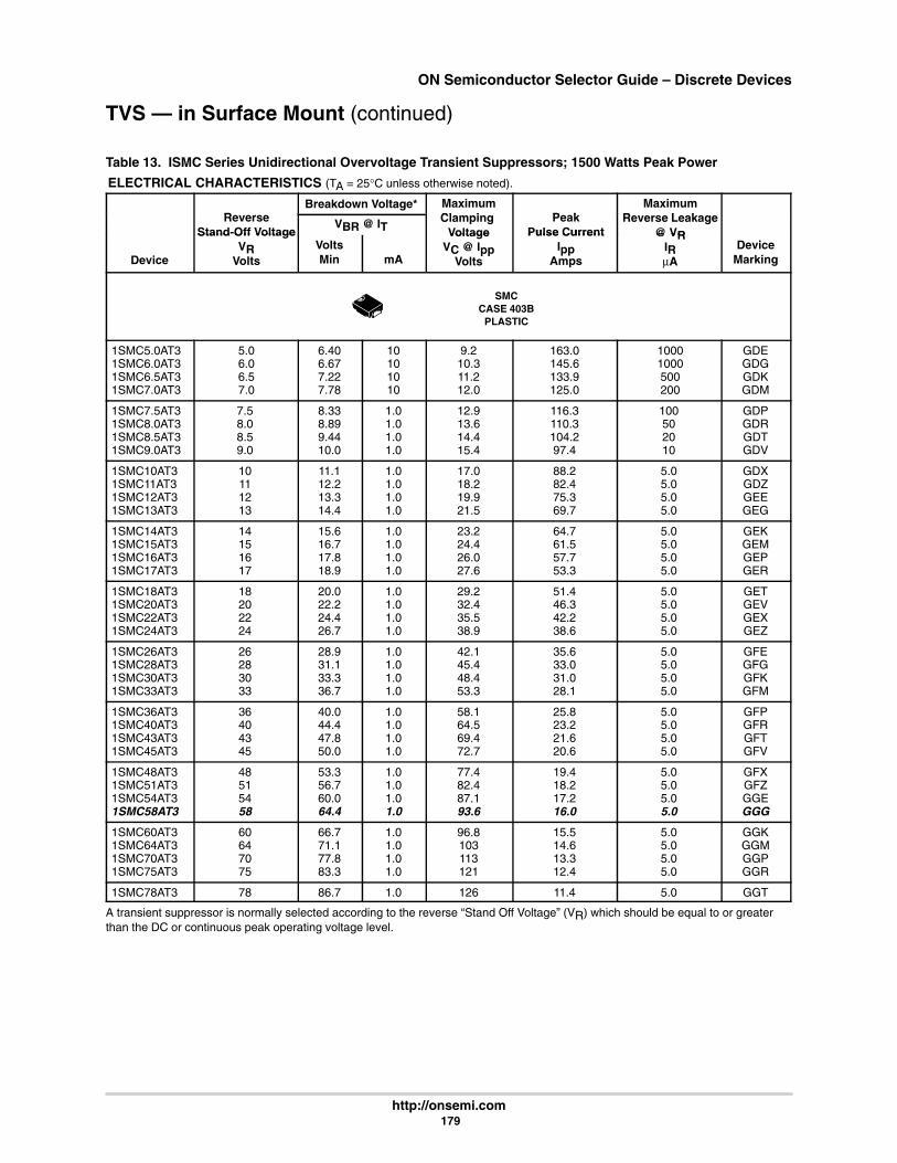
ON Semiconductor Selector Guide – Discrete Devices
http://onsemi.com 179
TVS — in Surface Mount (continued)
Table 13. ISMC Series Unidirectional Overvoltage Transient Suppressors; 1500 Watts Peak Power
ELECTRICAL CHARACTERISTICS (TA = 25°C unless otherwise noted).
RBreakdown Voltage* Maximum
Cl i P kMaximum
R L kReverseStand-Off Voltage
VBR @ ITClamping
VoltagePeak
Pulse CurrentReverse Leakage
@ VR
Device
Stand Off VoltageVR
VoltsVoltsMin mA
VoltageVC @ Ipp
Volts
Pulse CurrentIpp
Amps
@ VRIRµA
DeviceMarking
SMCCASE 403B
PLASTIC
1SMC5.0AT31SMC6.0AT31SMC6.5AT31SMC7.0AT3
5.06.06.57.0
6.406.677.227.78
10101010
9.210.311.212.0
163.0145.6133.9125.0
10001000500200
GDEGDGGDKGDM
1SMC7.5AT31SMC8.0AT31SMC8.5AT31SMC9.0AT3
7.58.08.59.0
8.338.899.4410.0
1.01.01.01.0
12.913.614.415.4
116.3110.3104.297.4
100502010
GDPGDRGDTGDV
1SMC10AT31SMC11AT31SMC12AT31SMC13AT3
10111213
11.112.213.314.4
1.01.01.01.0
17.018.219.921.5
88.282.475.369.7
5.05.05.05.0
GDXGDZGEEGEG
1SMC14AT31SMC15AT31SMC16AT31SMC17AT3
14151617
15.616.717.818.9
1.01.01.01.0
23.224.426.027.6
64.761.557.753.3
5.05.05.05.0
GEKGEMGEPGER
1SMC18AT31SMC20AT31SMC22AT31SMC24AT3
18202224
20.022.224.426.7
1.01.01.01.0
29.232.435.538.9
51.446.342.238.6
5.05.05.05.0
GETGEVGEXGEZ
1SMC26AT31SMC28AT31SMC30AT31SMC33AT3
26283033
28.931.133.336.7
1.01.01.01.0
42.145.448.453.3
35.633.031.028.1
5.05.05.05.0
GFEGFGGFKGFM
1SMC36AT31SMC40AT31SMC43AT31SMC45AT3
36404345
40.044.447.850.0
1.01.01.01.0
58.164.569.472.7
25.823.221.620.6
5.05.05.05.0
GFPGFRGFTGFV
1SMC48AT31SMC51AT31SMC54AT31SMC58AT3
48515458
53.356.760.064.4
1.01.01.01.0
77.482.487.193.6
19.418.217.216.0
5.05.05.05.0
GFXGFZGGEGGG
1SMC60AT31SMC64AT31SMC70AT31SMC75AT3
60647075
66.771.177.883.3
1.01.01.01.0
96.8103113121
15.514.613.312.4
5.05.05.05.0
GGKGGMGGPGGR
1SMC78AT3 78 86.7 1.0 126 11.4 5.0 GGT
A transient suppressor is normally selected according to the reverse “Stand Off Voltage” (VR) which should be equal to or greaterthan the DC or continuous peak operating voltage level.

ON Semiconductor Selector Guide – Discrete Devices
http://onsemi.com 180
TVS — in Surface Mount (continued)
Table 14. 1.5 SMC Series Unidirectional Overvoltage Transient Suppressors; 1500 Watts Peak Power
ELECTRICAL CHARACTERISTICS (TA = 25°C unless otherwise noted) VF = 3.5 V Max, IF = 100 A for all types.
Breakdown Voltage Working Maximum Maximum
MaximumReverseVoltage
VBR @ ITVolts
gPeak
ReverseVoltage
ReverseLeakage@ VRWM
ReverseSurge
Current
g@ IRSM
(ClampingVoltage)
MaximumTemperatureCoefficient
Device Min Nom Max mAVRWMVolts
IRµA
IRSM
AmpsVRSMVolts
of VBR%/°C
DeviceMarking
SMCCASE 403B
PLASTIC
1.5SMC6.8AT31.5SMC7.5AT31.5SMC8.2AT31.5SMC9.1AT3
6.457.137.798.65
6.87.58.29.1
7.147.888.619.55
1010101
5.86.47.027.78
100050020050
143132124112
10.511.312.113.4
0.0570.0610.0650.068
6V8A7V5A8V2A9V1A
1.5SMC10AT31.5SMC11AT31.5SMC12AT31.5SMC13AT3
9.510.511.412.4
10111213
10.511.612.613.7
1111
8.559.410.211.1
10555
103969082
14.515.616.718.2
0.0730.0750.0780.081
10A11A12A13A
1.5SMC15AT31.5SMC16AT31.5SMC18AT31.5SMC20AT3
14.315.217.119
15161820
15.816.818.921
1111
12.813.615.317.1
5555
7167
59.554
21.222.525.227.7
0.0840.0860.0880.09
15A16A18A20A
1.5SMC22AT31.5SMC24AT31.5SMC27AT31.5SMC30AT3
20.922.825.728.5
22242730
23.125.228.431.5
1111
18.820.523.125.6
5555
49454036
30.633.237.541.4
0.0920.0940.0960.097
22A24A27A30A
1.5SMC33AT31.5SMC36AT31.5SMC39AT31.5SMC43AT3
31.434.237.140.9
33363943
34.737.841
45.2
1111
28.230.833.336.8
5555
333028
25.3
45.749.953.959.3
0.0980.0990.1
0.101
33A36A39A43A
1.5SMC47AT31.5SMC51AT31.5SMC56AT31.5SMC62AT3
44.748.553.258.9
47515662
49.453.658.865.1
1111
40.243.647.853
5555
23.221.419.517.7
64.870.17785
0.1010.1020.1030.104
47A51A56A62A
1.5SMC68AT31.5SMC75AT31.5SMC82AT31.5SMC91AT3
64.671.377.986.5
68758291
71.478.886.195.5
1111
58.164.170.177.8
5555
16.314.613.312
92103113125
0.1040.1050.1050.106
68A75A82A91A
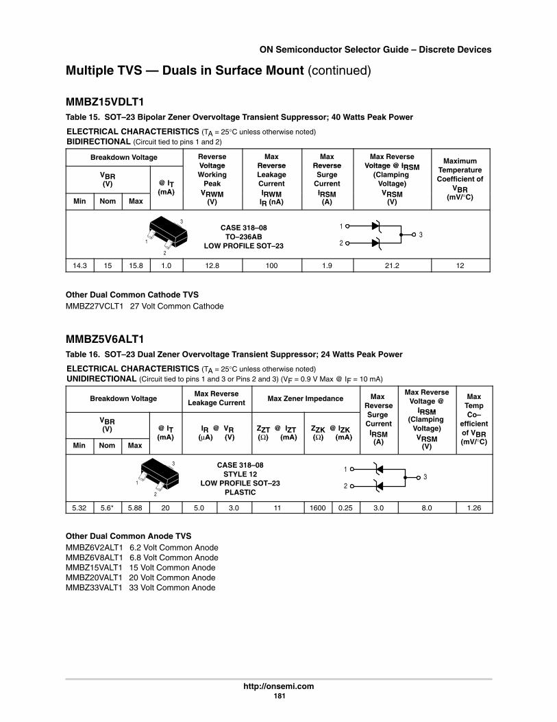
ON Semiconductor Selector Guide – Discrete Devices
http://onsemi.com 181
Multiple TVS — Duals in Surface Mount (continued)
MMBZ15VDLT1Table 15. SOT–23 Bipolar Zener Overvoltage Transient Suppressor; 40 Watts Peak Power
ELECTRICAL CHARACTERISTICS (TA = 25°C unless otherwise noted)BIDIRECTIONAL (Circuit tied to pins 1 and 2)
Breakdown Voltage ReverseVoltage
MaxReverse
MaxReverse
Max ReverseVoltage @ IRSM
Maximum
VBR(V) @ IT
(mA)
VoltageWorking
PeakVRWM
ReverseLeakageCurrentIRWM
ReverseSurge
CurrentIRSM
Voltage @ IRSM(Clamping
Voltage)VRSM
TemperatureCoefficient of
VBR
Min Nom Max(mA) VRWM
(V)IRWMIR (nA)
IRSM(A)
VRSM(V)
BR(mV/°C)
1
2
3CASE 318–08
TO–236ABLOW PROFILE SOT–23
13
2
14.3 15 15.8 1.0 12.8 100 1.9 21.2 12
Other Dual Common Cathode TVSMMBZ27VCLT1 27 Volt Common Cathode
MMBZ5V6ALT1Table 16. SOT–23 Dual Zener Overvoltage Transient Suppressor; 24 Watts Peak Power
ELECTRICAL CHARACTERISTICS (TA = 25°C unless otherwise noted)UNIDIRECTIONAL (Circuit tied to pins 1 and 3 or Pins 2 and 3) (VF = 0.9 V Max @ IF = 10 mA)
Breakdown VoltageMax Reverse
Leakage Current Max Zener Impedance Max ReverseS
Max ReverseVoltage @
IRSM
MaxTempC
VBR(V) @ IT
(mA) IR @ VR (µA) (V)
ZZT @ IZT (Ω) (mA)
ZZK @ IZK (Ω) (mA)
Surge CurrentIRSM
IRSM(Clamping
Voltage)VRSM
Co–efficientof VBR
Min Nom Max(mA) (µA) (V) (Ω) (mA) (Ω) (mA)
(A)VRSM
(V)(mV/°C)
1
2
3 CASE 318–08STYLE 12
LOW PROFILE SOT–23PLASTIC
13
2
5.32 5.6* 5.88 20 5.0 3.0 11 1600 0.25 3.0 8.0 1.26
Other Dual Common Anode TVSMMBZ6V2ALT1 6.2 Volt Common AnodeMMBZ6V8ALT1 6.8 Volt Common AnodeMMBZ15VALT1 15 Volt Common AnodeMMBZ20VALT1 20 Volt Common AnodeMMBZ33VALT1 33 Volt Common Anode

ON Semiconductor Selector Guide – Discrete Devices
http://onsemi.com 182
Multiple TVS — Quads in Surface Mount (continued)
MMQA SeriesTable 17. SC–59 Quad Transient Voltage Suppressor; 24 Watts Peak Power
ELECTRICAL CHARACTERISTICS (TA = 25°C unless otherwise noted)
UNIDIRECTIONAL (Circuit tied to pins 1, 2, and 5; Pins 2, 3, and 5; Pins 2, 4, and 5; or Pins 2, 5, and 6)
(VF = 0.9 V Max @ IF = 10 mA)
Breakdown VoltageMax Reverse
Leakage Current Max ZenerImpedance
MaxReverseS rge
MaxReverse
Voltage @IRSM
MaxTempCoef–
VZT (V) @ IZT IR VR
pSurge
CurrentIRSM
(ClampingVoltage)
ficientof VZ
Device Min Nom Max (mA) (nA) (V)ZZT @ IZT (Ω) (mA)
IRSM(A)
VRSM(V) (mV/°C)
CASE 318F-02STYLE 1
SC-59 PLASTIC
1
2
3
6
5
4
12
3
45
6
MMQA5V6T1,T3 5.32 5.6 5.88 1.0 2000 3.0 400 3.0 8.0 1.26
MMQA6V2T1,T3 5.89 6.2 6.51 1.0 700 4.0 300 2.66 9.0 10.6
MMQA6V8T1,T3 6.46 6.8 7.14 1.0 500 4.3 300 2.45 9.8 10.9
MMQA12VT1,T3 11.4 12 12.6 1.0 75 9.1 80 1.39 17.3 14
MMQA13VT1,T3 12.4 13 13.7 1.0 75 9.8 80 1.29 18.6 15
MMQA15VT1,T3 14.3 15 15.8 1.0 75 11 80 1.1 21.7 16
MMQA18VT1,T3 17.1 18 18.9 1.0 75 14 80 0.923 26 19
MMQA20VT1,T3 19 20 21 1.0 75 15 80 0.84 28.6 20.1
MMQA21VT1,T3 20 21 22.1 1.0 75 16 80 0.792 30.3 21
MMQA22VT1,T3 20.9 22 23.1 1.0 75 17 80 0.758 31.7 22
MMQA24VT1,T3 22.8 24 25.2 1.0 75 18 100 0.694 34.6 25
MMQA27VT1,T3 25.7 27 28.4 1.0 75 21 125 0.615 39 28
MMQA30VT1,T3 28.5 30 31.5 1.0 75 23 150 0.554 43.3 32
MMQA33VT1,T3 31.4 33 34.7 1.0 75 25 200 0.504 48.6 37

http://onsemi.com 183
TMOS Power MOSFETs
In Brief . . .Page
TMOS Power MOSFETs 183. . . . . . . . . . . . . . . . . . . . . . TMOS Power MOSFETs Numbering System 184. . SO–8 MiniMOS 186. . . . . . . . . . . . . . . . . . . . . . . . . . . . EZFET SO–8 Power MOSFETs 187. . . . . . . . . . . . . . Micro8 187. . . . . . . . . . . . . . . . . . . . . . . . . . . . . . . . . . SOT–223 187. . . . . . . . . . . . . . . . . . . . . . . . . . . . . . . . . TSOP–6 187. . . . . . . . . . . . . . . . . . . . . . . . . . . . . . . . . . SOT–23 188. . . . . . . . . . . . . . . . . . . . . . . . . . . . . . . . . . SC–70/SOT–323 188. . . . . . . . . . . . . . . . . . . . . . . . . . DPAK 188. . . . . . . . . . . . . . . . . . . . . . . . . . . . . . . . . . . . D2PAK 189. . . . . . . . . . . . . . . . . . . . . . . . . . . . . . . . . . . TO–220AB 190. . . . . . . . . . . . . . . . . . . . . . . . . . . . . . . . TO–247 191. . . . . . . . . . . . . . . . . . . . . . . . . . . . . . . . . . TO–264 191. . . . . . . . . . . . . . . . . . . . . . . . . . . . . . . . . . Current Limit MOSFETs — SMARTDISCRETES 192. . . . . . . . . . . . . . . . . . . . .
Insulated Gate Bipolar Transistors (IGBTs) 192. . . .
ON Semiconductors has been one of the premiersuppliers of Power MOSFETs since the early 1980s andcontinues to develop new MOSFET products with thelowest possible on–resistance per silicon area.Continuing R&D has created MOSFET products that aremanufactured with the same precision and versatility asthe most advanced integrated circuits. The followingnew advances have been made in the area of silicontechnology.• New WaveFET high cell density MOSFETs
utilizing ON Semiconductors’s latest MOSFETtechnology provide ultra–low RDS(on) in both P– andN–channels in the SO–8 and DPAK surface mountpackages and industry standard TO–220 package.
• New ESD FETs include monolithic back–to–backZener diodes protecting the gate from ESD as well asproviding extremely low RDS(on) in surface mountand through–hole packages.Advances in packaging technology provide the end
users with the broadest portfolio of surface mountMOSFETs in the industry. Advances in surface mountpackaging from largest to smallest include:• New Micro8 eight leaded low profile package for
both single and dual MOSFETS.• New TSOP–6 six leaded low profile package
housing dual and single MOSFETs.• New SC–70 three leaded package (smaller than a
SOT–23) for single MOSFET chips.

ON Semiconductor Selector Guide – Discrete Devices
http://onsemi.com 184
TMOSPower MOSFETs
TMOS Power MOSFETs Numbering SystemWherever possible, ON Semiconductors has used the following numbering systems for TMOS power MOSFET products.
MTP75N06HD
CIRCUIT IDENTIFIERX FOR ENGINEERING SAMPLES
TMOST FOR TMOSL FOR SMARTDISCRETESG FOR IGBT (except MGSF)
PACKAGE TYPEP FOR PLASTIC TO–220D FOR DPAKA FOR TO–220 ISOLATEDW FOR TO–247B FOR D2PAKY FOR TO–264
CURRENT
OPTIONAL SUFFIX:L FOR LOGIC LEVELE FOR ENERGY RATEDT4 FOR TAPE & REEL (DPAK/D2PAK)RL FOR TAPE & REEL (DPAK)HD FOR HIGH CELL DENSITYV FOR TMOS V (FIVE)
VOLTAGE RATING DIVIDED BY 10
CHANNEL POLARITY, N OR P
Example of exceptions: MTD/MTP3055EExample of exceptions: MTD/MTP2955E
MMSF4P01HDR1
CIRCUIT IDENTIFIER
TMOSM FOR MINIATURE
PACKAGE TYPEDF — DUAL FET (SO–8)SF — SINGLE FET (SO–8)FT — FET TRANSISTOR (SOT–223)MTSF — SINGLE FET (Micro8)MTDF — DUAL FET (Micro8)MGSF – TSOP–6, SOT–23
CURRENT
OPTIONAL SUFFIX:E FOR ENERGY RATEDHD FOR HIGH CELL DENSITYL FOR LOGIC LEVELV FOR TMOS V (FIVE)Z FOR ESD
VOLTAGE RATING DIVIDED BY 10
CHANNEL POLARITY, N OR PC FOR COMPLEMENTARY
SO–8 (MiniMOS), Micro8, SOT–223,and TSOP–6 Power MOSFETs
R1 AND R2 FOR TAPE & REELMiniMOS
T1 AND T3 FOR TAPE & REELSOT–223

ON Semiconductor Selector Guide – Discrete Devices
http://onsemi.com 185
Part Numbering System
MMSF4205
CIRCUIT IDENTIFIER
TMOSM FOR MINIATURE
PACKAGE TYPEDF — DUAL FET (SO–8)SF — SINGLE FET (SO–8)FT — FET TRANSISTOR (SOT–223)MTSF — SINGLE FET (MICRO8)MTDF — DUAL FET (MICRO8)MGSF — TSOP–6, SOT–23
EVEN — N–CHANNELODD — P–CHANNEL
VOLTAGE 10
TECHNOLOGY5 — TRENCH4 — HD3e3 — HD31 — HD1

ON Semiconductor Selector Guide – Discrete Devices
http://onsemi.com 186
CASE 751–06SO–8
CASE 318E–04SOT–223
CASE 318G–02TSOP–6
CASE 340G–02TO–264
CASE 340K–01TO–247
CASE 369A–13TO–252, DPAK
CASE 221A–09TO–220AB
CASE 418B–03TO–264, D2PAK
CASE 419–02SC–70
CASE 846A–02Micro8
Packages Not to Scale
CASE 318–09SOT–23
TM
Table 1. SO-8 (MiniMOS) — Case 751–06
V(BR)DSSMax RDS(on) @ VGS ID
(3)
PD(1,2)V(BR)DSS(Volts)
Min10 V(mΩ)
4.5 V(mΩ)
2.7 V(mΩ)
ID(cont)Amps Device(3)
PD( , )
(Watts)Max Configuration
60 100 200 — 3.3 MMDF3N06HD 2.0 Dual N–Channel
50 300 500 — 1.5 MMDF1N05E Dual N–Channel
40 80 100 — 3.4 MMDF3N04HD
30 12.5 20 — 12 MMSF3300 2.5 Single N–Channel
28 40 — 8 MMSF7N03HD Single N–Channel
40 50 — 5 MMSF5N03HD Single N–Channel
50/85 80/160 — 5.5/4.4 MMDF4C03HD Complementary
70 75 — 3 MMDF3N03HD 2.0 Dual N–Channel
70/200(4) 75/300 — 2 MMDF2C03HD Complementary
85 160 — 4 MMDF4P03HD Dual P–Channel
35 50 — 6 MMDFS6N303 MOSFET/Schottky
100 110 — 3 MMSF3P03HD 1.5 Single P–Channel
200 300 — 2 MMDF2P03HD Dual P–Channel
20 — 35 49* 6 MMDF6N02HD 2.5 Dual N–Channel
25 40 — 8.2 MMSF5N02HD Single N–Channel
90 100 — 3 MMDF3N02HD 2.0 Dual N–Channel
100 200 — 2 MMDF2N02E
250 400 — MMDF2P02E Dual P–Channel
— 45 55 4 MMDF4N01HD Dual N–Channel
90/160(4) 100/180(4) — MMDF2C02HD Complementary
100/250(4) 200/400(4) — MMDF2C02E
— 30 45 6.4 MMSF5P02HD 2.5 Single P–Channel
75 95 — 3 MMSF3P02HD 1.5 Dual P–Channel
160 180 — 2 MMDF2P02HD
12 — 45/180 55/220(4) 2 MMDF2C01HD 2.0 Complementary
— 80 90 4 MMSF4P01HD 2.5 Single P–Channel
— 180 220 2 MMDF2P01HD 2.0 Dual P–Channel(1) TC = 25°C(2) Power rating when mounted on a 2″ square FR-4 board.(3) Available in tape and reel only — R1 suffix = 500/reel, R2 suffix = 2500/reel.(4) N-Channel/P-Channel RDS(on) with the minimum recommended footprint.* RDS(on) @ VGS other than listed.
Devices listed in bold, italic are ON Semiconductor preferred devices.

ON Semiconductor Selector Guide – Discrete Devices
http://onsemi.com 187
Table 2. EZFET — SO–8 Power MOSFETs with Zener Gate Protection — Case 751–06
V(BR)DSSMax RDS(on) @ VGS ID (cont)
(3)PD(1,2) VGSV(BR)DSS
(Volts) Min 10 V (mΩ) 4.5 V (mΩ) 2.7 V (mΩ)ID (cont)
Amps Device(3)PD
(Watts) MaxVGS
(Volts) Max Configuration
50 300 500 — 2 MMDF2N05Z 2.0 ±15 Dual N–Channel
30 13 18 — 10 MMSF10N03Z 1.6 Single N–Channel
20 — 15 19 6 MMSF10N02Z 2.5 ±10 Single N–Channel
— 27 35 5 MMDF7N02Z 2.0 ±12 Dual N–Channel
30 30 40 — 7 MMDF7N03Z 1.6 ±15 Dual N–Channel(1) TC = 25°C(2) Power rating when mounted on 1” square copper pad on FR–4/G–10 Board (VGS = 4.5 V, @ steady state).(3) Available in tape and reel only — R1 suffix = 500/reel, R2 suffix = 2500/reel.
Table 3. Micro8 — Case 846A–02
V(BR)DSSMax RDS(on) @ VGS ID (cont)
(3)PD(1,2)V(BR)DSS
(Volts) Min 10 V (mΩ) 4.5 V (mΩ) 2.7 V (mΩ)ID (cont)
Amps Device(3)PD
(Watts) Max Configuration
30 120 160 — 1 MTDF1N03HD 1.25 Dual N–Channel
90 150 — 2.4 MTSF2P03HD 1.8 Single P–Channel
40 60 — 3 MTSF3N03HD Single N–Channel
20 — 120 160 1.7 MTDF1N02HD 1.25 Dual N–Channel
— 175 280 1.6 MTDF1P02HD Dual P–Channel
— 160 190 1.5 MTSF1P02HD 1.8 Single P–Channel
— 90 120 2.4 MTSF2P02HD 1.8 Single P–Channel
— 40 50 3.8 MTSF3N02HD 1.8 Single N–Channel
— 120/175 160/280 1.7 MTDF1C02HD 1.25 Complementary(1) TC = 25°C(2) Power rating when mounted on 1” square copper pad on FR–4/G–10 Board (VGS = 4.5 V, @ steady state).(3) Available in tape and reel only — R1 suffix = 500/reel, R2 suffix = 2500/reel.
Table 4. SOT-223 — Case 318E–04
V(BR)DSSMax RDS(on) @ VGS ID (cont)
(4)PD(1)V(BR)DSS
(Volts) Min 10 V (Ω) 4.5 V (Ω) 2.7 V (Ω)ID (cont)
Amps Device(4)PD
(Watts) Max Polarity
100 0.25 — — 1 MMFT1N10E 0.8(3) N–Channel
60 — 0.14 — 1.5 MMFT3055VL(2) N–Channel
0.13 — — 1.7 MMFT3055V N–Channel
0.30 — — 1.2 MMFT2955E P–Channel
20 — 0.15 — 2 MMFT2N02EL(2) N–Channel
30 0.1 — 5.2 MMFT5P03HD 3.1 P–Channel(1) TC = 25°C(2) RDS(on) @ VGS = 5 V(3) Power rating when mounted on an FR-4 glass epoxy printed circuit board with the minimum recommended footprint.(4) Available in tape and reel only — T1 suffix = 1000/reel, T3 suffix = 4000/reel.
Table 5. TSOP–6 — Case 318G–02
V(BR)DSSMax RDS(on) @ VGS ID (cont) PD(1,2) VGSV(BR)DSS
(Volts) Min 10 V (Ω) 4.5 V (Ω) 2.5 V (Ω)ID (cont)
Amps DevicePD
(Watts) MaxVGS
(Volts) Min Polarity
30 0.065 0.095 1.75 MGSF3454X 0.95 1.0 N–Channel
— 4.2 MGSF3454V 2.0 N–Channel
0.1 190 1.5 MGSF3455X 0.4 P–Channel
3.5 MGSF3455V 2.0 P–Channel
20 0.07 0.095 1.7 MGSF3442X 0.5 0.6 N–Channel
— 4.0 MGSF3442V 2.0 N–Channel
0.90 .135 1.5 MGSF3441X 0.95 0.45 P–Channel
3.3 MGSF3441V 2.0 P–Channel(1) TC = 25°C(2) Power rating when mounted on an FR-4 glass epoxy printed circuit board with the minimum recommended footprint.

ON Semiconductor Selector Guide – Discrete Devices
http://onsemi.com 188
Table 6. SOT–23 — Case 318–09
V(BR)DSSMax RDS(on) @ VGS ID (cont) PD(1,2) VGSV(BR)DSS
(Volts) Min 10 V (Ω) 4.5 V (Ω) 2.5 V (Ω)ID (cont)
Amps DevicePD
(Watts) MaxVGS
(Volts) Min Polarity
60 5.0 — 0.5 MMBF170LT1 0.225 0.8 N–Channel
7.5 0.12 2N7002LT1 1.0 N–Channel
50 — 10 0.1 BSS84 P–Channel
30 0.1 0.145 1.0 MGSF1N03LT1 0.4 N–Channel
20 0.09 0.13 — MGSF1N02LT1 N–Channel
1.0 1.4 0.3 MMBF0201NLT1 0.225 N–Channel
— 0.26 0.5 0.75 MGSF1P02ELT1 0.4 0.7 P–Channel
0.35 0.5 — MGSF1P02LT1 1.0 P–Channel
1.4 3.5 0.25 MMBF0202PLT1 0.225 P–Channel(1) TC = 25°C(2) Power rating when mounted on an FR-4 glass epoxy printed circuit board with the minimum recommended footprint.
Table 7. SC–70 / SOT–323 — Case 419–02
V(BR)DSSMax RDS(on) @ VGS ID (cont) PD(1,2) VGSV(BR)DSS
(Volts) Min 10 V (Ω) 4.5 V (Ω) 2.7 V (Ω)ID (cont)
Amps DevicePD
(Watts) MaxVGS
(Volts) Min Polarity
20 1.0 1.4 — 0.3 MMBF2201NT1 0.15 1.0 N–Channel
2.2 3.5 — MMBF2202PT1 P–Channel(1) TC = 25°C(2) Power rating when mounted on an FR-4 glass epoxy printed circuit board with the minimum recommended footprint.
Table 8. DPAK — Case 369A–13 (TO–252)
V(BR)DSSMax RDS(on) @ VGS ID (cont)
(4)PD(1,3)V(BR)DSS
(Volts) Min 10 V (Ω) 5.0 V (Ω) 2.7 V (Ω)ID (cont)
Amps Device(4)PD
(Watts) Max
DPAK — N-Channel
800 12 — — 1 MTD1N80E 48
500 5 — — 1 MTD1N50E 40
3.60 — — 2 MTD2N50E
400 3.50 — — 2 MTD2N40E
250 1.40 — — 3 MTD3N25E
200 1.20 — — 4 MTD4N20E
100 0.25 — — 9 MTD9N10E
0.14 — — 14 MTD14N10E 72
60 — 0.18 — 12 MTD3055VL 48
0.12 — — 15 MTD15N06V 55
0.15 — — 8 MTD3055V 48
0.045 — — 20 MTD20N06HD 40
— 0.045 — 20 MTD20N06HDL
0.080 — — 20 MTD20N06V 60
30 0.010 0.016* — 10.8 MTD3302
16 20* — 25 MTD1312 72
— 0.035 — 20 MTD20N03HDL 74
0.022 0.029* — 20 MTD1302 74
DPAK — P-Channel
500 15.0 — — 1 MTD1P50E 50
400 8 — — 1 MTD1P40E
60 0.45 — — 5 MTD5P06V 40
0.20 — — 12 MTD2955V 60
— 175 — 20 MTD20P06HDL 72
30 — 0.099 — 19 MTD20P03HDL 75(1) TC = 25°C(3) Power rating when mounted on an FR-4 glass epoxy printed circuit board with the minimum recommended footprint.(4) Available in tape and reel — add T4 suffix to part number.(5) ESD protected to 4 kV.* RDS(on) @ VGS other than specified.
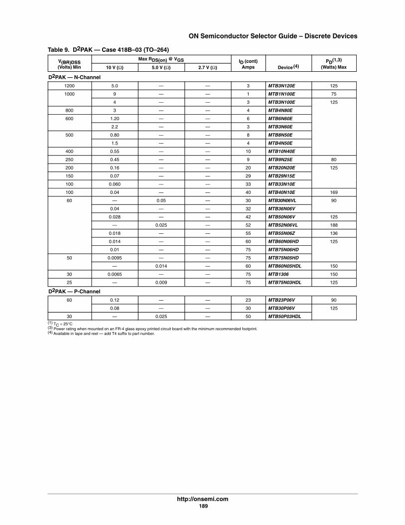
ON Semiconductor Selector Guide – Discrete Devices
http://onsemi.com 189
Table 9. D2PAK — Case 418B–03 (TO–264)
V(BR)DSSMax RDS(on) @ VGS ID (cont)
(4)PD(1,3)V(BR)DSS
(Volts) Min 10 V (Ω) 5.0 V (Ω) 2.7 V (Ω)ID (cont)
Amps Device(4)PD
(Watts) Max
D2PAK — N-Channel
1200 5.0 — — 3 MTB3N120E 125
1000 9 — — 1 MTB1N100E 75
4 — — 3 MTB3N100E 125
800 3 — — 4 MTB4N80E
600 1.20 — — 6 MTB6N60E
2.2 — — 3 MTB3N60E
500 0.80 — — 8 MTB8N50E
1.5 — — 4 MTB4N50E
400 0.55 — — 10 MTB10N40E
250 0.45 — — 9 MTB9N25E 80
200 0.16 — — 20 MTB20N20E 125
150 0.07 — — 29 MTB29N15E
100 0.060 — — 33 MTB33N10E
100 0.04 — — 40 MTB40N10E 169
60 — 0.05 — 30 MTB30N06VL 90
0.04 — — 32 MTB36N06V
0.028 — — 42 MTB50N06V 125
— 0.025 — 52 MTB52N06VL 188
0.018 — — 55 MTB55N06Z 136
0.014 — — 60 MTB60N06HD 125
0.01 — — 75 MTB75N06HD
50 0.0095 — — 75 MTB75N05HD
— 0.014 — 60 MTB60N05HDL 150
30 0.0065 — — 75 MTB1306 150
25 — 0.009 — 75 MTB75N03HDL 125
D2PAK — P-Channel
60 0.12 — — 23 MTB23P06V 90
0.08 — — 30 MTB30P06V 125
30 — 0.025 — 50 MTB50P03HDL(1) TC = 25°C(3) Power rating when mounted on an FR-4 glass epoxy printed circuit board with the minimum recommended footprint.(4) Available in tape and reel — add T4 suffix to part number.

ON Semiconductor Selector Guide – Discrete Devices
http://onsemi.com 190
Table 10. TO-220AB — Case 221A–09
V(BR)DSSMax RDS(on) @ VGS ID (cont) PD(1)V(BR)DSS
(Volts) Min 10 V (Ω) 5.0 V (Ω) 2.7 V (Ω)ID (cont)
Amps DevicePD
(Watts) Max
TO-220AB — N-Channel
1200 5.0 — — 3 MTP3N120E 125
1000 9 — — 1 MTP1N100E 75
4.0 — — 3 MTP3N100E 125
800 3 — — 4 MTP4N80E
600 8 — — 1 MTP1N60E 50
3.80 — — 2 MTP2N60E
2.20 — — 3 MTP3N60E 75
1.20 — — 6 MTP6N60E 125
500 5 — — 1 MTP1N50E 50
3 — — 3 MTP3N50E 50
1.50 — — 4 MTP4N50E 75
0.80 — — 8 MTP8N50E 125
400 3.50 — — 2 MTP2N40E 50
1.80 — — 4 MTP4N40E 50
1 — — 5 MTP5N40E 75
0.55 — — 10 MTP10N40E 125
250 1.4 — — 3 MTP3N25E 40
0.45 — — 9 MTP9N25E 75
0.25 — — 16 MTP16N25E 125
200 0.70 — — 7 MTP7N20E 75
0.16 — — 20 MTP20N20E 125
150 0.07 — — 29 MTP29N15E 125
0.13 — — 20 MTP20N15E
100 0.25 — — 10 MTP10N10E 75
0.14 — — 14 IRF530 78
0.16 — — 12 MTP12N10E 75
0.077 — — 27 IRF540 145
0.070 — — 27 MTP27N10E 125
0.060 — — 33 MTP33N10E 150
0.04 — — 40 MTP40N10E 169
60 — 0.18 — 12 MTP3055VL 48
0.15 — — 12 MTP3055V
0.12 — — 15 MTP15N06V 55
— 0.05 — 30 MTP30N06VL 90
0.04 — — 32 MTP36N06V
— 0.032 — 42 MTP50N06VL 150
0.028 — — 42 MTP50N06V
0.022 — — 52 MTP52N06V 186
— 0.025 — 52 MTP52N06VL 188
0.014 — — 60 MTP60N06HD 150
0.01 — — 75 MTP75N06HD
50 — 0.10 — 15 MTP15N05EL 75
0.0095 — — 75 MTP75N05HD 150
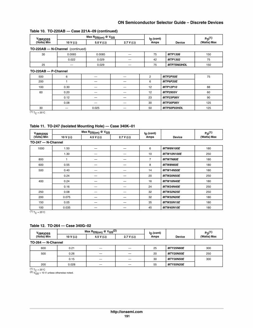
ON Semiconductor Selector Guide – Discrete Devices
http://onsemi.com 191
Table 10. TO-220AB — Case 221A–09 (continued)
V(BR)DSSMax RDS(on) @ VGS ID (cont) PD(1)V(BR)DSS
(Volts) Min 10 V (Ω) 5.0 V (Ω) 2.7 V (Ω)ID (cont)
Amps DevicePD( )
(Watts) Max
TO-220AB — N-Channel (continued)
30 0.0065 0.0085 — 75 MTP1306 150
0.022 0.029 — 42 MTP1302 75
25 — 0.029 — 75 MTP75N03HDL 150
TO-220AB — P-Channel
500 6 — — 2 MTP2P50E 75
200 1 — — 6 MTP6P20E
100 0.30 — — 12 MTP12P10 88
60 0.20 — — 12 MTP2955V 60
0.12 — — 23 MTP23P06V 90
0.08 — — 30 MTP30P06V 125
30 — 0.025 — 50 MTP50P03HDL 125(1) TC = 25°C
Table 11. TO-247 (Isolated Mounting Hole) — Case 340K–01
V(BR)DSSMax RDS(on) @ VGS ID (cont) PD(1)V(BR)DSS
(Volts) Min 10 V (Ω) 4.5 V (Ω) 2.7 V (Ω)ID (cont)
Amps DevicePD
(Watts) Max
TO-247 — N-Channel
1000 1.50 — — 6 MTW6N100E 180
1.30 — — 10 MTW10N100E 250
800 1 — — 7 MTW7N80E 180
600 0.55 — — 8 MTW8N60E 180
500 0.40 — — 14 MTW14N50E 180
0.24 — — 20 MTW20N50E 250
400 0.24 — — 16 MTW16N40E 180
0.16 — — 24 MTW24N40E 250
250 0.08 — — 32 MTW32N25E 250
200 0.075 — — 32 MTW32N20E 180
150 0.05 — — 35 MTW35N15E 180
100 0.035 — — 45 MTW45N10E 180(1) TC = 25°C
Table 12. TO-264 — Case 340G–02
V(BR)DSSMax RDS(on) @ VGS(2)
ID (cont) PD(1)V(BR)DSS(Volts) Min 10 V (Ω) 4.5 V (Ω) 2.7 V (Ω)
ID (cont)Amps Device
PD(Watts) Max
TO-264 — N-Channel
600 0.21 — — 25 MTY25N60E 300
500 0.26 — — 20 MTY20N50E 250
0.15 — — 30 MTY30N50E 300
200 0.028 — — 55 MTY55N20E(1) TC = 25°C(2) VGS = 10 V unless otherwise noted.
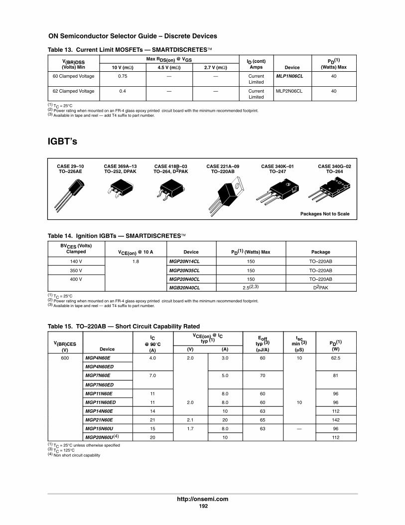
ON Semiconductor Selector Guide – Discrete Devices
http://onsemi.com 192
Table 13. Current Limit MOSFETs — SMARTDISCRETES
V(BR)DSSMax RDS(on) @ VGS ID (cont) PD(1)V(BR)DSS
(Volts) Min 10 V (mΩ) 4.5 V (mΩ) 2.7 V (mΩ)ID (cont)
Amps DevicePD
(Watts) Max
60 Clamped Voltage 0.75 — — CurrentLimited
MLP1N06CL 40
62 Clamped Voltage 0.4 — — CurrentLimited
MLP2N06CL 40
(1) TC = 25°C(2) Power rating when mounted on an FR-4 glass epoxy printed circuit board with the minimum recommended footprint.(3) Available in tape and reel — add T4 suffix to part number.
IGBT’s
CASE 340G–02TO–264
CASE 340K–01TO–247
CASE 369A–13TO–252, DPAK
CASE 221A–09TO–220AB
CASE 418B–03TO–264, D2PAK
Packages Not to Scale
CASE 29–10TO–226AE
Table 14. Ignition IGBTs — SMARTDISCRETESBVCES (Volts)
Clamped VCE(on) @ 10 A Device PD(1) (Watts) Max Package
140 V 1.8 MGP20N14CL 150 TO–220AB
350 V MGP20N35CL 150 TO–220AB
400 V MGP20N40CL 150 TO–220AB
MGB20N40CL 2.5(2,3) D2PAK
(1) TC = 25°C(2) Power rating when mounted on an FR-4 glass epoxy printed circuit board with the minimum recommended footprint.(3) Available in tape and reel — add T4 suffix to part number.
Table 15. TO–220AB — Short Circuit Capability Rated
V(BR)CES
IC@ 90°C
VCE(on) @ ICtyp (1) Eoff
typ (3)tsc
min (3) PD(1)(BR)CES(V) Device
@ 90 C(A) (V) (A)
typ ( )
(J/A)min ( )
(S)D(W)
600 MGP4N60E 4.0 2.0 3.0 60 10 62.5
MGP4N60ED
MGP7N60E 7.0 5.0 70 81
MGP7N60ED
MGP11N60E 11 8.0 60 96
MGP11N60ED 11 2.0 8.0 60 10 96
MGP14N60E 14 10 63 112
MGP21N60E 21 2.1 20 65 142
MGP15N60U 15 1.7 8.0 63 — 96
MGP20N60U (4) 20 10 112(1) TC = 25°C unless otherwise specified(3) TC = 125°C(4) Non short circuit capability
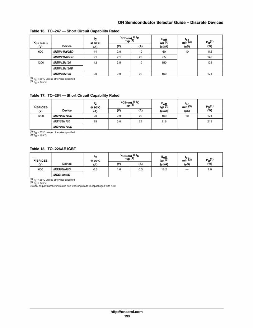
ON Semiconductor Selector Guide – Discrete Devices
http://onsemi.com 193
Table 16. TO–247 — Short Circuit Capability Rated
V(BR)CES
IC@ 90°C
VCE(on) @ ICtyp (1) Eoff
typ (3)tsc
min (3) PD(1)(BR)CES(V) Device
@ 90 C(A) (V) (A)
typ ( )
(J/A)min ( )
(S)D(W)
600 MGW14N60ED 14 2.0 10 60 10 112
MGW21N60ED 21 2.1 20 65 142
1200 MGW12N120 12 3.5 10 150 125
MGW12N120D
MGW20N120 20 2.9 20 160 174(1) TC = 25°C unless otherwise specified(3) TC = 125°C
Table 17. TO–264 — Short Circuit Capability Rated
V(BR)CES
IC@ 90°C
VCE(on) @ ICtyp (1) Eoff
typ (3)tsc
min (3) PD(1)(BR)CES(V) Device
@ 90 C(A) (V) (A)
typ ( )
(J/A)min ( )
(S)D(W)
1200 MGY20N120D 20 2.9 20 160 10 174
MGY25N120 25 3.0 25 216 212
MGY25N120D
(1) TC = 25°C unless otherwise specified(3) TC = 125°C
Table 18. TO–226AE IGBT
V(BR)CES
IC@ 90°C
VCE(on) @ ICtyp (1) Eoff
typ (3)tsc
min (3) PD(1)(BR)CES(V) Device
@ 90 C(A) (V) (A)
typ ( )
(J/A)min ( )
(S)D(W)
600 MGS05N60D 0.3 1.6 0.3 16.2 — 1.0
MGS13002D(1) TC = 25°C unless otherwise specified(3) TC = 125°CD suffix on part number indicates free wheeling diode is copackaged with IGBT
ON Semiconductor Selector Guide – Discrete Devices
http://onsemi.com 194
Bipolar Power Transistors
In Brief . . .Page
Bipolar Power Transistors 195. . . . . . . . . . . . . . . . . . . . . Selection by Package 195. . . . . . . . . . . . . . . . . . . . . .
Plastic TO–220AB 196. . . . . . . . . . . . . . . . . . . . . . . Plastic TO–225AA Type(Formerly TO–126 Type) 197. . . . . . . . . . . . . . . .
SO–8 – Surface Mount Packages 197. . . . . . . . . DPAK – Surface Mount Power Packages 198. . . D2PAK – Surface Mount Packages 198. . . . . . . . SOT–223 – Surface Mount Packages 198. . . . . . Large Plastic TO–264 198. . . . . . . . . . . . . . . . . . . . Plastic Isolated TO–220 Type 199. . . . . . . . . . . . . Metal TO–204AA (Formerly TO–3),TO–204AE 200. . . . . . . . . . . . . . . . . . . . . . . . . . . .
Audio 201. . . . . . . . . . . . . . . . . . . . . . . . . . . . . . . . . . . . Electronic Lamp Ballasts 202. . . . . . . . . . . . . . . . . . . .
ON Semiconductor’s broad line of Bipolar PowerTransistors includes discrete and Darlington transistorsin a variety of packages from the popular surface mountDPAK at 1.75 watts to the 250 watt TO-3 and TO–264.New products include the MJE/MJF 18000 series forlamp ballast and power supplies, MJW16212 — a new1500 V deflection transistor for video monitorapplications, and high performance audio output devicesin the TO–264 package. We have the broadest line ofBipolar Power Transistors in the industry and theON Semiconductor commitment to quality and totalcustomer satisfaction to go with them.

ON Semiconductor Selector Guide – Discrete Devices
http://onsemi.com 195
BIPOLAR POWER TRANSISTORS SELECTOR GUIDESELECTION BY PACKAGE
PackageIC Range(Amps)
VCE Range(Volts)
PD(Watts)
TO-204AA(TO-3)
CASE 1-074-30 40-1500 90-250
TO-204AECASE 197A-05 50–80 60-1000 150-300
DPAKCASE 369-07 0.5-10 40-400 12.5-20
DPAKCASE 369A-13 0.5-10 40-400 12.5-20
TO-220ABCASE 221A-09 0.5-15 30-1800 30-125
ISOLATEDTO-220 TYPE
CASE 221D-021-12 80-450 20-45
TO-225AA(TO-126 TYPE)
CASE 77-090.3-5.0 25-400 12.5-40
SOT–223CASE 318E–04 3.0 30 2.0 (1)
SO–8CASE 751-06 3.0 30 2.0 (2)
TO-264CASE 340G-02 15-16 200-250 250
D2PAKCASE 418B-03 5.0–8.0 80–1000 50–65 W
(1) Tested on 1″ sq. FR4 Board(2) Tested on 1″ sq., 2 oz. copper

ON Semiconductor Selector Guide – Discrete Devices
http://onsemi.com 196
Table 1. PLASTIC TO–220AB — CASE 221A–09, Style 1
Device Type Resistive Switching
ICContAmpsMax
VCEO(sus)VoltsMin NPN PNP
hFEMin/Max
@ ICAmp
tsµs
Max
tfµs
Max@ ICAmp
fTMHzMin
PD (Case)Watts
@ 25°C
1 100 TIP29C TIP30C 15/75 1 0.6 typ 0.3 typ 1 3 30
250 TIP47 30/150 0.3 2 typ 0.18 typ 0.3 10 40
400 TIP50 MJE5731A 30/150 0.3 2 typ 0.18 typ 0.3 10 40
2 100 TIP112 (2) TIP117 (2) 500 min 2 1.7 typ 1.3 typ 2 25(1) 50
450/1000 BUX85 30 0.1 3.5 1.4 1 4 50
450/1000 MJE18002 14/34 0.2 3 0.17 1 12 typ 40
3 100 TIP31C TIP32C 25 min 1 0.6 typ 0.3 typ 1 3 40
4 80 D44C12 D45C12 40/120 0.2 1 40 typ 30
400/700 MJE13005 6/30 3 3 0.7 3 4 60
5 100 TIP122 (2) TIP127 (2) 1k min 3 1.5 typ 1.5 typ 4 4(1) 75
400/700 BUL45 14/34 0.3 1.7 0.15 1 12 typ 75
450/1000 MJE16002 5 min 5 3 0.3 3 80
550/1200 MJE18204 18/35 0.5 2.75 0.2 2 12 75
6 100 TIP41C TIP42C 15/75 3 0.4 typ 0.15 typ 3 3 65
400/700 BUL146 14/34 0.5 1.75 0.15 3 14 typ 100
7 70 2N6292 2N6107 30/150 2 0.4 typ 0.15 typ 3 4 40
150 BU407 30 min 1.5 0.75 5 10 60
8 100 BDX53C (2) BDX54C (2) 750 min 3
TIP102 (2) TIP107 (2) 1k/20k 3 1.5 typ 1.5 typ 3 4(1) 80
150 MJE15030 MJE15031 20 min 4 30 50
250 MJE15032 MJE15033 50 min 1 30 50
350 MJE13007 5/30 5 3 0.7 5 80
MJE5852 15 min 2 2 0.5 4 80
400/700 BUL147 14/34 1 2.5 0.18 2 14 typ 125
10 60 MJE3055T MJE2955T 20/70 4 75
80 2N6388 (2) 2N6668 (2) 1k/20k 5 20 (1) 65
D44H11 D45H11 40 min 4 0.5 typ 0.14 typ 5 50 typ 50
100 BDX33C (2) BDX34C (2) 750 min 3 3 70
12 400/700 MJE13009 6/30 8 3 0.7 8 4 100
15 80 D44VH10 D45VH10 20 min 4 0.5 0.09 8 50 typ 83
100 BDW42 (2) BDW47 (2) 1k min 5 1 typ 1.5 typ 5 4 85(1) |hFE| @ 1 MHz(2) Darlington
Devices listed in bold, italic are ON Semiconductor preferred devices.
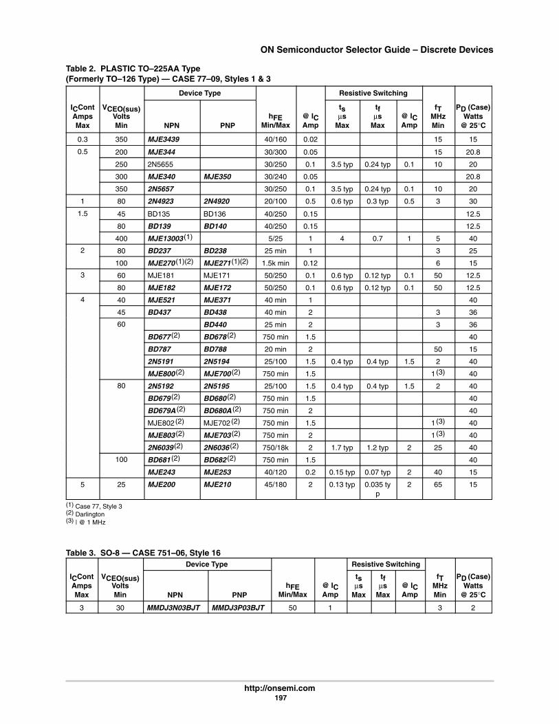
ON Semiconductor Selector Guide – Discrete Devices
http://onsemi.com 197
Table 2. PLASTIC TO–225AA Type(Formerly TO–126 Type) — CASE 77–09, Styles 1 & 3
Device Type Resistive Switching
ICContAmpsMax
VCEO(sus)VoltsMin NPN PNP
hFEMin/Max
@ ICAmp
tsµs
Max
tfµs
Max@ ICAmp
fTMHzMin
PD (Case)Watts
@ 25°C
0.3 350 MJE3439 40/160 0.02 15 15
0.5 200 MJE344 30/300 0.05 15 20.8
250 2N5655 30/250 0.1 3.5 typ 0.24 typ 0.1 10 20
300 MJE340 MJE350 30/240 0.05 20.8
350 2N5657 30/250 0.1 3.5 typ 0.24 typ 0.1 10 20
1 80 2N4923 2N4920 20/100 0.5 0.6 typ 0.3 typ 0.5 3 30
1.5 45 BD135 BD136 40/250 0.15 12.5
80 BD139 BD140 40/250 0.15 12.5
400 MJE13003 (1) 5/25 1 4 0.7 1 5 40
2 80 BD237 BD238 25 min 1 3 25
100 MJE270 (1)(2) MJE271(1)(2) 1.5k min 0.12 6 15
3 60 MJE181 MJE171 50/250 0.1 0.6 typ 0.12 typ 0.1 50 12.5
80 MJE182 MJE172 50/250 0.1 0.6 typ 0.12 typ 0.1 50 12.5
4 40 MJE521 MJE371 40 min 1 40
45 BD437 BD438 40 min 2 3 36
60 BD440 25 min 2 3 36
BD677 (2) BD678 (2) 750 min 1.5 40
BD787 BD788 20 min 2 50 15
2N5191 2N5194 25/100 1.5 0.4 typ 0.4 typ 1.5 2 40
MJE800 (2) MJE700 (2) 750 min 1.5 1(3) 40
80 2N5192 2N5195 25/100 1.5 0.4 typ 0.4 typ 1.5 2 40
BD679 (2) BD680 (2) 750 min 1.5 40
BD679A (2) BD680A (2) 750 min 2 40
MJE802(2) MJE702(2) 750 min 1.5 1(3) 40
MJE803 (2) MJE703 (2) 750 min 2 1(3) 40
2N6039 (2) 2N6036 (2) 750/18k 2 1.7 typ 1.2 typ 2 25 40
100 BD681 (2) BD682 (2) 750 min 1.5 40
MJE243 MJE253 40/120 0.2 0.15 typ 0.07 typ 2 40 15
5 25 MJE200 MJE210 45/180 2 0.13 typ 0.035 typ
2 65 15
(1) Case 77, Style 3(2) Darlington(3) | @ 1 MHz
Table 3. SO-8 — CASE 751–06, Style 16Device Type Resistive Switching
ICContAmpsMax
VCEO(sus)VoltsMin NPN PNP
hFEMin/Max
@ ICAmp
tsµs
Max
tfµs
Max@ ICAmp
fTMHzMin
PD (Case)Watts
@ 25°C
3 30 MMDJ3N03BJT MMDJ3P03BJT 50 1 3 2
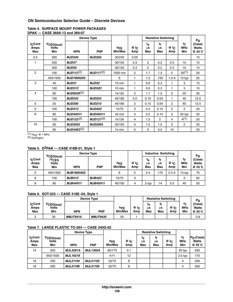
ON Semiconductor Selector Guide – Discrete Devices
http://onsemi.com 198
Table 4. SURFACE MOUNT POWER PACKAGESDPAK — CASE 369A-13 and 369-07
Device Type Resistive SwitchingPD
ICContAmpsMax
VCEO(sus)VoltsMin NPN PNP
hFEMin/Max
@ ICAmp
tsµs
Max
tfµs
Max@ ICAmp
fTMHzMin
PD(Case)Watts
@ 25°C
0.5 300 MJD340 MJD350 30/240 0.05 15
1 250 MJD47 30/150 0.3 2 0.2 0.3 10 15
400 MJD50 30/150 0.3 2 0.2 0.3 10 15
2 100 MJD112 (2) MJD117 (2) 1000 min 2 1.7 1.3 2 25(1) 20
450/1000 MJD18002D2 6 1 1.2 .150 1.0 A 13 typ 25
3 40 MJD31 MJD32 10 min 1 0.6 0.3 1 3 15
100 MJD31C MJD32C 10 min 1 0.6 0.3 1 3 15
4 80 MJD6039 (2) 1k/12k 2 1.7 1.2 2 25 20
100 MJD243 MJD253 40/180 0.2 0.16 0.04 1 40 12.5
5 25 MJD200 MJD210 45/180 2 0.15 0.04 2 65 12.5
6 100 MJD41C MJD42C 15/75 3 0.4 0.15 3 3 20
8 80 MJD44H11 MJD45H11 40 min 4 0.5 0.14 5 50 typ 20
100 MJD122 (2) MJD127 (2) 1k/12k 4 1.5 2 4 4(1) 20
10 60 MJD3055 MJD2955 20/100 4 1.5 1.5 3 2 20
80 MJD44E3 (2) 1k min 5 2 0.5 10 20(1) |hFE| @ 1 MHz(2) Darlington
Table 5. D2PAK — CASE 418B-01, Style 1
VCEO(s s)Device Type Inductive Switching
PDICContAmpsMax
VCEO(sus)/VCESVoltsMin NPN PNP
hFEMin/Max
@ ICAmp
tsµs
Max
tfµs
Max@ ICAmp
fTMHzMin
PD(Case)Watts
@ 25°C
5 450/1000 MJB18004D2 6 2 2.4 .175 2.5 A 13 typ 75
6 100 MJB41C MJB42C 15/75 3 3 65
8 80 MJB44H11 MJB45H11 40/100 4 .5 typ .14 5.0 40 50
Table 6. SOT-223 — CASE 318E–04, Style 1Device Type Resistive Switching PD
ICContAmpsMax
VCEO(sus)VoltsMin NPN PNP
hFEMin/Max
@ ICAmp
tsµs
Max
tfµs
Max@ ICAmp
fTMHzMin
PD(Case)Watts
@ 25°C
3 30 MMJT9410 MMJT9435 50 1 0.8
Table 7. LARGE PLASTIC TO-264 — CASE 340G-02Device Type Resistive Switching
ICContAmpsMax
VCEO(sus)VoltsMin NPN PNP
hFEMin/Max
@ ICAmp
tsµs
Max
tfµs
Max@ ICAmp
fTMHzMin
PD (Case)Watts
@ 25°C
15 200 MJL3281A MJL1302A 60/175 0.1 30 typ 200
650/1500 MJL16218 4/11 12 2.5 typ 170
16 250 MJL21194 MJL21193 25/75 8 4 200
16 250 MJL21196 MJL21195 25/75 8 4 200
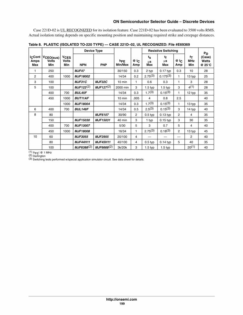
ON Semiconductor Selector Guide – Discrete Devices
http://onsemi.com 199
Case 221D-02 is UL RECOGNIZED for its isolation feature. Case 221D-02 has been evaluated to 3500 volts RMS.Actual isolation rating depends on specific mounting position and maintaining required strike and creepage distances.
Table 8. PLASTIC (ISOLATED TO-220 TYPE) — CASE 221D–02, UL RECOGNIZED: File #E69369
Device Type Resistive SwitchingPD
ICContAmpsMax
VCEO(sus)VoltsMin
VCESVoltsMin NPN PNP
hFEMin/Max
@ ICAmp
tsµs
Max
tfµs
Max@ ICAmp
fTMHzMin
PD(Case)Watts
@ 25°C
1 250 MJF47 30/150 0.3 2 typ 0.17 typ 0.3 10 28
2 400 1000 MJF18002 14/34 0.2 2.75(3) 0.175(3) 1 13 typ 25
3 100 MJF31C MJF32C 10 min 1 0.6 0.3 1 3 28
5 100 MJF122 (2) MJF127 (2) 2000 min 3 1.5 typ 1.5 typ 3 4(1) 28
400 700 BUL45F 14/34 0.3 1.7(3) 0.15(3) 1 12 typ 35
450 1000 BUT11AF 10 min .005 4 0.8 2.5 40
1000 MJF18004 14/34 0.3 1.7(3) 0.15(3) 1 13 typ 35
6 400 700 BUL146F 14/34 0.5 2.5(3) 0.15(3) 3 14 typ 40
8 80 MJF6107 30/90 2 0.5 typ 0.13 typ 2 4 35
150 MJF15030 MJF15031 40 min 3 1 typ 0.15 typ 3 30 35
400 700 MJF13007 5/30 5 3 0.7 5 4 40
450 1000 MJF18008 16/34 1 2.75(3) 0.18(3) 2 13 typ 45
10 60 MJF3055 MJF2955 20/100 4 — — — 2 40
80 MJF44H11 MJF45H11 40/100 4 0.5 typ 0.14 typ 5 40 35
100 MJF6388 (2) MJF6668 (2) 3k/20k 3 1.5 typ 1.5 typ 20(1) 40(1) |hFE| @ 1 MHz(2) Darlington(3) Switching tests performed w/special application simulator circuit. See data sheet for details.

ON Semiconductor Selector Guide – Discrete Devices
http://onsemi.com 200
Table 9. METAL TO–204AA (Formerly TO–3) — CASE 1–07TO–204AE — CASE 197A–05, Style 1
Device Type Resistive SwitchingPD
ICContAmpsMax
VCEO(sus)Volts
Min(8) NPN PNPhFE
Min/Max@ ICAmp
tsµs
Max
tfµs
Max@ ICAmp
fTMHzMin
PD(Case)Watts
@ 25°C
4 250 MJ15020 MJ15021 30 min 1 20 150
10 80 2N3716 2N3792 30 min 3 0.3 typ 0.4 typ 5 4 150
MJ3001(2) MJ2501 (2) 1k min 5 150
250 MJ15011 MJ15012 20/100 2 200
400 MJ10012 (2) 100/2k 6 15 15 6 175
12 100 2N6059 (2) 2N6052 (2) 750/18k 6 1.6 typ 1.5 typ 6 4(1) 150
15 60 2N3055 MJ2955 20/70 4 0.7 typ 0.3 typ 4 2.5 115
120 MJ15015 MJ15016 20/70 4 0.7 typ 0.3 typ 4 1 180
140 MJ15001 MJ15002 25/150 4 2 200
400/650 MJ16110 6/20 15 0.8 typ 0.1 typ 10 175
16 140 2N3773 2N6609 15/60 8 1.1 typ 1.5 typ 8 4 150
200 MJ15022 MJ15023 15/60 8 5 250
250 MJ21194 MJ21193 25/75 8 4 250
250 MJ21196 MJ21195 25/75 8 5 250
20 80 2N6286(2) 750/18k 10 2.5 typ 2.5 typ 10 4(1) 160
100 2N6284 (2) 2N6287 (2) 750/18k 10 2.5 typ 2.5 typ 10 4(1) 160
140 MJ15003 MJ15004 25/150 5 2 250
400 MJ13333 10/60 5 4 0.7 10 175
500 MJ10009 (2) 30/300 10 2 0.6 10 8(1) 175
25 60 2N5885 2N5883 20/100 10 1 0.8 10 4 200
150 2N6341 30/120 10 1 0.25 10 40 200
30 60 2N5302 2N4399 15/60 15 2 1 10 2 200
100 MJ802 MJ4502 25/100 7.5 2 200
120 MJ11016 (2) MJ11015 (2) 1k min 20 4(1) 200
400/1000 BUX98 8 min 20 3 0.8 20 250
450/850 MJ16020 5 min 30 1.8 0.2 20 250
40 400 MJ10023 (2) 50/600 10 2.5 0.9 20 250
50 80 2N5686 2N5684 15/60 25 0.5 typ 0.3 typ 25 2 300
120 MJ11032 (2) MJ11033 (2) 400 min 50 300
125 BUV20 10 min 50 1.2 0.25 50 8 250
400 MJ10015 (2) 10 min 40 2.5 1 20 250
60 80 MJ14002 MJ14003 15/100 50 300(1) |hFE| @ 1 MHz(2) Darlington

ON Semiconductor Selector Guide – Discrete Devices
http://onsemi.com 201
Audio GENERAL DESIGN CURVES FOR POWER AUDIO OUTPUT STAGES
500
300
100
7050
30
1010 30 50 100 300 500 1000
16 OHMS
8 OHMS
4 OHMS
OUTPUT POWER (WATTS)
V(B
R)
CEO
(VO
LTS)
V(BR)CEO Required on Output and Driver Transistorversus
Output Power for 4, 8 and 18 Ohm Loads
8 OHMS
4 OHMS
50
30
10
5.0
3.0
1.010 30 50 100 300 500 1000
OUTPUT POWER (WATTS)PE
AK O
UTP
UT
CU
RR
ENT
(AM
PS)
Output Transistor Peak Collector Currentversus
Output Power for 4, 8 and 16 Ohm Loads
16 OHMS
Another important parameter that must be considered before selecting the output transistors is the safe–operating areathese devices must withstand. For a complete discussion see Application Note AN485.
Table 10. Recommended Power Transistors for Audio/Servo Loads
RMSPowerOutput NPN PNP Case
PDWatts
@ 25°C VCEO
hFE @Min/Max
ICAmps
fTMHzTyp
ISBVolts/Amps
To 25W MJE15030 MJE15031 TO–220 50 150 20 min 4 30 14/3.6
MJE15032 MJE15033 TO–220 50 250 50 min 1 40 50/1
25 to 50W 2N3055A — TO–204 120 120 20/70 4 3 60/2
MJ15001 MJ15002 TO–204 200 140 25/150 4 3 40/5
50 to 100W MJ15015 MJ15016 TO–204 180 120 20/70 4 3 60/3
MJ15003 MJ15004 TO–204 250 140 25/150 5 3 100/1
MJ15020 MJ15021 TO–204 150 250 30 min 1 20 50/3
Over 100W MJ15024 MJ15025 TO–204 250 250 15/60 8 8 80/2.2
MJL3281A MJL1302A 340G–02 150 200 60/175 7 30 40/4MJ21194 MJ21193 TO–204 250 250 25/75 8 7 100/2MJL21194 MJL21193 340G–02 200 200 25/75 8 7 100/2MJ21195 MJ21195 TO–204 250 250 25/75 8 7 100/2MJL21196 MJL21195 340G–02 200 200 25/75 8 7 100/2
The Power Transistors shown are provided for reference only and show device capability. The final choice of thePower Transistors used is left to the circuit designer and depends upon the particular safe–operating area required andthe mounting and heat sinking configuration used.
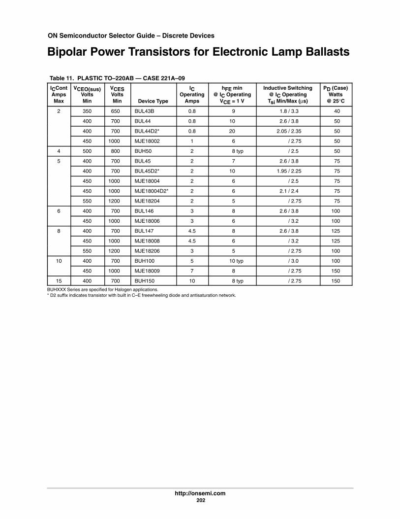
ON Semiconductor Selector Guide – Discrete Devices
http://onsemi.com 202
Bipolar Power Transistors for Electronic Lamp Ballasts
Table 11. PLASTIC TO–220AB — CASE 221A–09
ICContAmpsMax
VCEO(sus)VoltsMin
VCESVoltsMin Device Type
ICOperating
Amps
hFE min@ IC Operating
VCE = 1 V
Inductive Switching@ IC OperatingTsi Min/Max (µs)
PD (Case)Watts
@ 25°C
2 350 650 BUL43B 0.8 9 1.8 / 3.3 40
400 700 BUL44 0.8 10 2.6 / 3.8 50
400 700 BUL44D2* 0.8 20 2.05 / 2.35 50
450 1000 MJE18002 1 6 / 2.75 50
4 500 800 BUH50 2 typ 8 typ / 2.5 50
5 400 700 BUL45 2 7 2.6 / 3.8 75
400 700 BUL45D2* 2 10 1.95 / 2.25 75
450 1000 MJE18004 2 6 / 2.5 75
450 1000 MJE18004D2* 2 6 2.1 / 2.4 75
550 1200 MJE18204 2 5 / 2.75 75
6 400 700 BUL146 3 8 2.6 / 3.8 100
450 1000 MJE18006 3 6 / 3.2 100
8 400 700 BUL147 4.5 8 2.6 / 3.8 125
450 1000 MJE18008 4.5 6 / 3.2 125
550 1200 MJE18206 3 5 / 2.75 100
10 400 700 BUH100 5 typ10 typ / 3.0 100
450 1000 MJE18009 7 8 / 2.75 150
15 400 700 BUH150 10 typ 8 typ / 2.75 150
BUHXXX Series are specified for Halogen applications.* D2 suffix indicates transistor with built in C–E freewheeling diode and antisaturation network.
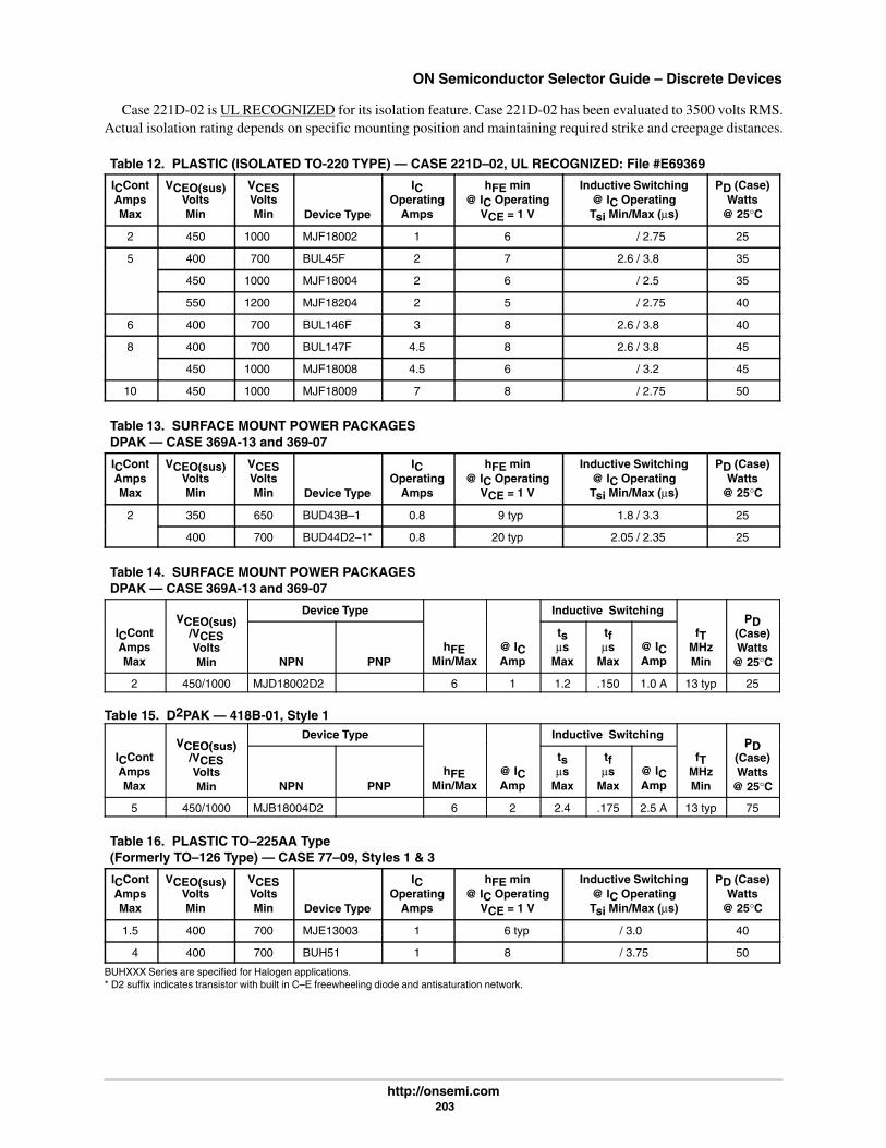
ON Semiconductor Selector Guide – Discrete Devices
http://onsemi.com 203
Case 221D-02 is UL RECOGNIZED for its isolation feature. Case 221D-02 has been evaluated to 3500 volts RMS.Actual isolation rating depends on specific mounting position and maintaining required strike and creepage distances.
Table 12. PLASTIC (ISOLATED TO-220 TYPE) — CASE 221D–02, UL RECOGNIZED: File #E69369
ICContAmpsMax
VCEO(sus)VoltsMin
VCESVoltsMin Device Type
ICOperating
Amps
hFE min@ IC Operating
VCE = 1 V
Inductive Switching@ IC OperatingTsi Min/Max (µs)
PD (Case)Watts
@ 25°C
2 450 1000 MJF18002 1 6 / 2.75 25
5 400 700 BUL45F 2 7 2.6 / 3.8 35
450 1000 MJF18004 2 6 / 2.5 35
550 1200 MJF18204 2 5 / 2.75 40
6 400 700 BUL146F 3 8 2.6 / 3.8 40
8 400 700 BUL147F 4.5 8 2.6 / 3.8 45
450 1000 MJF18008 4.5 6 / 3.2 45
10 450 1000 MJF18009 7 8 / 2.75 50
Table 13. SURFACE MOUNT POWER PACKAGESDPAK — CASE 369A-13 and 369-07
ICContAmpsMax
VCEO(sus)VoltsMin
VCESVoltsMin Device Type
ICOperating
Amps
hFE min@ IC Operating
VCE = 1 V
Inductive Switching@ IC OperatingTsi Min/Max (µs)
PD (Case)Watts
@ 25°C
2 350 650 BUD43B–1 0.8 9 typ 1.8 / 3.3 25
400 700 BUD44D2–1* 0.8 20 typ 2.05 / 2.35 25
Table 14. SURFACE MOUNT POWER PACKAGESDPAK — CASE 369A-13 and 369-07
VCEO(s s)Device Type Inductive Switching
PDICContAmpsMax
VCEO(sus)/VCESVoltsMin NPN PNP
hFEMin/Max
@ ICAmp
tsµs
Max
tfµs
Max@ ICAmp
fTMHzMin
PD(Case)Watts
@ 25°C
2 450/1000 MJD18002D2 6 1 1.2 .150 1.0 A 13 typ 25
Table 15. D2PAK — 418B-01, Style 1
VCEO(s s)Device Type Inductive Switching
PDICContAmpsMax
VCEO(sus)/VCESVoltsMin NPN PNP
hFEMin/Max
@ ICAmp
tsµs
Max
tfµs
Max@ ICAmp
fTMHzMin
PD(Case)Watts
@ 25°C
5 450/1000 MJB18004D2 6 2 2.4 .175 2.5 A 13 typ 75
Table 16. PLASTIC TO–225AA Type(Formerly TO–126 Type) — CASE 77–09, Styles 1 & 3
ICContAmpsMax
VCEO(sus)VoltsMin
VCESVoltsMin Device Type
ICOperating
Amps
hFE min@ IC Operating
VCE = 1 V
Inductive Switching@ IC OperatingTsi Min/Max (µs)
PD (Case)Watts
@ 25°C
1.5 400 700 MJE13003 1 typ6 typ / 3.0 40
4 400 700 BUH51 1 8 / 3.75 50
BUHXXX Series are specified for Halogen applications.* D2 suffix indicates transistor with built in C–E freewheeling diode and antisaturation network.
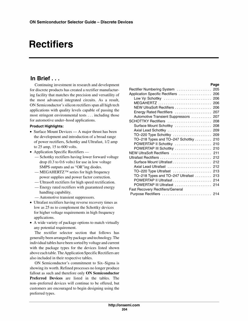
ON Semiconductor Selector Guide – Discrete Devices
http://onsemi.com 204
Rectifiers
In Brief . . .Page
Rectifier Numbering System 205. . . . . . . . . . . . . . . . . . . Application Specific Rectifiers 206. . . . . . . . . . . . . . . . . .
Low VF Schottky 206. . . . . . . . . . . . . . . . . . . . . . . . . . MEGAHERTZ 206. . . . . . . . . . . . . . . . . . . . . . . . . . . . . NEW UltraSoft Rectifiers 206. . . . . . . . . . . . . . . . . . . . Energy Rated Rectifiers 207. . . . . . . . . . . . . . . . . . . . Automotive Transient Suppressors 207. . . . . . . . . . .
SCHOTTKY Rectifiers 208. . . . . . . . . . . . . . . . . . . . . . . . Surface Mount Schottky 208. . . . . . . . . . . . . . . . . . . . Axial Lead Schottky 209. . . . . . . . . . . . . . . . . . . . . . . . TO–220 Type Schottky 209. . . . . . . . . . . . . . . . . . . . . TO–218 Types and TO–247 Schottky 210. . . . . . . . . POWERTAP II Schottky 210. . . . . . . . . . . . . . . . . . . . POWERTAP III Schottky 210. . . . . . . . . . . . . . . . . . . .
NEW UltraSoft Rectifiers 211. . . . . . . . . . . . . . . . . . . . . . Ultrafast Rectifiers 212. . . . . . . . . . . . . . . . . . . . . . . . . . . .
Surface Mount Ultrafast 212. . . . . . . . . . . . . . . . . . . . . Axial Lead Ultrafast 212. . . . . . . . . . . . . . . . . . . . . . . . TO–220 Type Ultrafast 213. . . . . . . . . . . . . . . . . . . . . TO–218 Types and TO–247 Ultrafast 213. . . . . . . . . POWERTAP II Ultrafast 214. . . . . . . . . . . . . . . . . . . . . POWERTAP III Ultrafast 214. . . . . . . . . . . . . . . . . . . .
Fast Recovery Rectifiers/GeneralPurpose Rectifiers 214. . . . . . . . . . . . . . . . . . . . . . . . . . .
Continuing investment in research and developmentfor discrete products has created a rectifier manufactur-ing facility that matches the precision and versatility ofthe most advanced integrated circuits. As a result,ON Semiconductor’s silicon rectifiers span all high techapplications with quality levels capable of passing themost stringent environmental tests . . . including thosefor automotive under–hood applications.
Product Highlights:
• Surface Mount Devices — A major thrust has been the development and introduction of a broad range of power rectifiers, Schottky and Ultrafast, 1/2 amp to 25 amp, 15 to 600 volts.
• Application Specific Rectifiers —— Schottky rectifiers having lower forward voltage
drop (0.3 to 0.6 volts) for use in low voltage SMPS outputs and as “OR”ing diodes.
— MEGAHERTZ series for high frequency power supplies and power factor correction.
— Ultrasoft rectifiers for high speed rectification.— Energy rated rectifiers with guaranteed energy
handling capability.— Automotive transient suppressors.
• Ultrafast rectifiers having reverse recovery times aslow as 25 ns to complement the Schottky devices for higher voltage requirements in high frequencyapplications.
• A wide variety of package options to match virtuallyany potential requirement.The rectifier selector section that follows has
generally been arranged by package and technology. Theindividual tables have been sorted by voltage and currentwith the package types for the devices listed shownabove each table. The Application Specific Rectifiers arealso included in their respective tables.
ON Semiconductor’s commitment to Six–Sigma isshowing its worth. Refined processes no longer producefallout as such and therefore only ON SemiconductorPreferred Devices are listed in the tables. Thenon–preferred devices will continue to be offered, butcustomers are encouraged to begin designing using thepreferred types.

ON Semiconductor Selector Guide – Discrete Devices
http://onsemi.com 205
VR
RECTIFIER NUMBERING SYSTEM
PART NUMBER KEY XXX X XX XX XX X
PREFIX
R = REVERSEL = LOW VFE = ENERGY
SUFFIX
(TYPE DESIGNATOR)
F = FULLY ISOLATEDA = SURFACE MT (SMA)S = SURFACE MT (SMB/SMC)D = DPAKB = D2PAKH = MEGAHERTZM = POWERMITEP = POWERTAP
IO(X10 EXCEPTSCHOTTKY)
(DUAL DESIGNATOR)
PREFIX KEY MUR = ULTRA FAST RECTIFIERMBR = (SCHOTTKY) BARRIER RECTIFIERMR = STANDARD & FAST RECOVERYMSR = ULTRASOFT
SUFFIX KEY CT = CENTER TAP (DUAL) TO–220, POWERTAP, DPAK, D2PAKPT = CENTER TAP (DUAL) TO–218 PACKAGEWT = CENTER TAP (DUAL) TO–247–1 = STRAIGHT LEAD D2PAK
EXAMPLE: MUR 30 20 WTULTRAFAST 30 AMP 200 V CENTER TAP (DUAL) TO–247
EXAMPLE: MBR 30 45 WTSCHOTTKY 30 AMP 45 V CENTER TAP (DUAL) TO–247
XX
PACKAGINGDESIGNATOR*
*For available packaging options consult Sales Office or see Data Sheet.
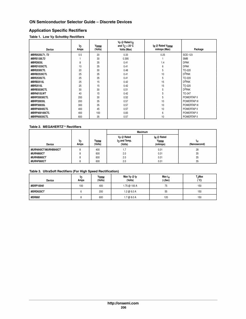
ON Semiconductor Selector Guide – Discrete Devices
http://onsemi.com 206
Application Specific Rectifiers
Table 1. Low VF Schottky Rectifiers
DeviceIO
AmpsVRRM(Volts)
VF @ Rated IOand TC = 25°C
Volts (Max)IR @ Rated VRRM
mAmps (Max) Package
MBR0520LT1, T3 0.5 20 0.33 0.25 SOD-123MBRS130LT3 1 30 0.395 1 SMBMBRD835L 8 35 0.41 1.4 DPAKMBRD1035CTL 10 35 0.41 6 DPAKMBR2030CTL 20 30 0.48 5 TO-220MBRB2535CTL 25 35 0.41 10 D2PAKMBR2535CTL 25 35 0.41 5 TO-220MBRB2515L 25 15 0.42 15 D2PAKMBR2515L 25 15 0.42 15 TO-220MBRB3030CTL 30 30 0.51 5 D2PAKMBR4015LWT 40 15 0.42 5 TO-247MBRP20030CTL 200 30 0.52 5 POWERTAP IIMBRP20035L 200 35 0.57 10 POWERTAP IIIMBRP30035L 300 35 0.57 10 POWERTAP IIIMBRP40045CTL 400 45 0.57 10 POWERTAP IIMBRP400100CTL 400 100 0.83 6 POWERTAP IIMBRP60035CTL 600 35 0.57 10 POWERTAP II
Table 2. MEGAHERTZ Rectifiers
Maximum
DeviceIO
AmpsVRRM(Volts)
VF @ RatedIO and Temp.
(Volts)
IR @ RatedVRRM
(mAmps)trr
(Nanosecond)
MURH840CT/MURHB840CT 8 400 1.7 0.01 28MURH860CT 8 600 2.0 0.01 35MURHB860CT 8 600 2.0 0.01 35MURHF860CT 8 600 2.0 0.01 35
Table 3. UltraSoft Rectifiers (For High Speed Rectification)
DeviceIO
AmpsVRRM(Volts)
Max VF @ IF(Volts)
Max trr(ηSec)
TJMax(°C)
MSRP10040 100 400 1.75 @ 100 A 75 150
MSRD620CT 6 200 1.2 @ 6.0 A 55 150
MSR860 8 600 1.7 @ 8.0 A 120 150

ON Semiconductor Selector Guide – Discrete Devices
http://onsemi.com 207
Application Specific Rectifiers (continued)
Table 4. Energy Rated Rectifiers
DeviceIO
AmpsVRRM(Volts)
Max VF @ Rated unless Noted(Volts)
IR @ VRRM(mAmps)
Waval(MJ)
MUR180E 1.0 800 1.75 10 10
MUR1100E 1.0 1000 1.75 10 10
MUR480E 4.0 800 1.75 25 20
MUR4100E 4.0 1000 1.75 25 20
MUR880E 8.0 800 1.8 25 20
MUR8100E 8.0 1000 1.8 25 20
MUR10120E 10 1200 2.2 @ 6.5 A 100 20
MUR10150E 10 1500 2.5 @ 6.5 A 100 20
MUR5150E 5.0 1500 2.4 50 20
Table 5. Automotive Transient Suppressors
DeviceIO
AmpsVRRM(Volts)
Max VF @ IF(Volts)
IRSMAmps
TJMax(°C)
MR2535L 6.0 20 1.1 @ 100 A 62 @ 10 mS 175
MR2835S 32 23 1.1 @ 100 A 62 @ 10 mS 175
MR4027N, P 40 18 1.1 @ 100 A 110 @ 10 mS 200
MR4045N, P 40 30 1.1 @ 100 A 55 @ 10 mS 200

ON Semiconductor Selector Guide – Discrete Devices
http://onsemi.com 208
SCHOTTKY Rectifiers
Table 6. Surface Mount Schottky Rectifiers
VRRM(Volts)
IO(1)
(Amperes)IO RatingCondition Device
Max VF @ iFTC = 25°C
(Volts)IFSM
(Amperes)
TJMax(°C)
Max IR(2)
TJ = 25°C(mA)
Max IR(3)
(mA) Package
20 0.5 TL = 90°C MBR0520LT1MBR0520LT3
0.310 @ 0.1 A0.385 @ 0.5 A
5 125 .075 @ 10 V.250 @ 20 V
5 @ 10 V8 @ 20 V
30 0.5 TL = 100°C MBR0530T1MBR0530T3
0.375 @ 0.1 A0.430 @ 0.5 A
5 125 .020 @ 15 V.130 @ 30 V
— CASE 425-04(SOD-123)
Cathode = Band40 0.5 TL = 110°C MBR0540T1
MBR0540T30.53 @ 0.5 A 5 150 .010 @ 20 V
.020 @ 40 V—
Cathode = Band
20 1 TC = 130°C MBRM120ET3 0.455 @ 0.1 A0.530 @ 1.0 A
50 150 0.010 @ 20 V 1.6 @ 20 V
20 1 Ttab ≤ 100°C MBRM120LT3 0.36 @ 0.1 A0.45 @ 1 A
50 125 0.4 @ 20 V N/A CASE 457–04(POWERMITE)
40 1 Ttab ≤ 100°C MBRM140T3 0.39 @ 0.1 A0.55 @ 1 A
50 125 0.5 @ 40 V N/A
30 1 TC ≤ 105°C MBRA130LT3 0.41 @ 1 A0.47 @ 2 A
25 125 1.0 @ 30 V0.4 @ 15 V
25 @ 30 VCASE 403B–01
40 1 TC ≤ 100°C MBRA140T3 0.60 @ 1 A0.73 @ 2 A
25 125 1.0 @ 40 V0.2 @ 20 V
25 @ 40 V (SMA)
30 1 TL = 120°C MBRS130LT3 0.395 @ 1.0 A 40 125 1 10
40 1 TL = 115°C MBRS140T3 0.6 @ 1.0 A 40 125 1 10CASE 403 03
40 2 TC ≤ 95°C MBRS240LT3 0.43 @ 2 A0.53 @ 4 A
25 125 2.0 @ 40 V0.5 @ 20 V
60 @ 40 V40 @ 20 V
CASE 403-03(SMB)
Cathode = Notch40 2 TC = 103°C MBRS2040LT3 0.43 @ 2 A
0.50 @ 4 A70 125 0.80 @ 40 V
0.10 @ 20 V20 @ 40 V6.0 @ 20 V
Cathode = Notchor Polarity Band
100 1 TL = 120°C MBRS1100T3 0.75 @ 1.0 A 40 150 0.5 5
40 3 TL = 100°C MBRS340T3 0.525 @ 3.0 A 80 125 2 20 CASE 403A-03(SMC)
60 3 TL = 100°C MBRS360T3 0.74 @ 3.0 A 80 125 0.5 20(SMC)
Cathode = Notch
60 3 TC = 125°C MBRD360 0.60 @ 3.0 A 75 150 0.2 20 @ 125°C CASE 369A-13(DPAK)60 6 TC = 130°C MBRD660CT 0.70 @ 3.0 A 75 150 0.1 15 @ 125°C (DPAK)
35 8 TC = 100°C MBRD835L 0.40 @ 3.0 A0.51 @ 8.0 A
100 125 1.4 35 4
1
35 10 TC = 90°C MBRD1035CTL 0.49 @ 10 A 100 125 2 130 @ 125°C1
3
45 15 TC = 105°C MBRB1545CT 0.84 @ 15 A 150 150 0.1 15 @ 125°C
60 20 TC = 110°C MBRB2060CT 0.95 @ 20 A 150 150 0.15 150 @ 125°C 1
100 20 TC = 110°C MBRB20100CT 0.85 @ 10 A0.95 @ 20 A
150 150 0.1 6 @ 125°C
“CT” Suffix
1
34
200 20 TC = 125°C MBRB20200CT 1.0 @ 20 A 150 150 1 50 @ 125°CCT Suffix
15 25 TC = 90°C MBRB2515L 0.45 @ 25 A 150 100 15 200 @ 70°C CASE 418B-0341
35 25 TC = 110°C MBRB2535CTL 0.47 @ 12.5 A0.55 @ 25 A
150 125 10 500 @ 125°C (D2PAK)
Non-“CT”
4
3
1
45 25 TC = 130°C MBRB2545CT 0.82 @ 30 A 150 150 0.2 40 @ 125°C4
Non- CTSuffix
30 30 TC = 115°C MBRB3030CT 0.54 @ 15 A0.67 @ 30 A
300 150 1.2 145 @ 150°C46 @ 10 V,
150°C
4
31
30 30 TC = 95°C MBRB3030CTL 0.45 @ 15 A0.51 @ 30 A
150 125 2 195 @ 125°C75 @ 10 V,
125°C
30 40 TC = 110°C MBRB4030 0.46 @ 20 A0.55 @ 40 A
300 150 1 150 @ 125°C
(1)IO is total device current capability.(2)VRRM unless noted(3)VRRM, TJ = 100°C unless noted
New Product
All devices listed are ON Semiconductor preferred devices
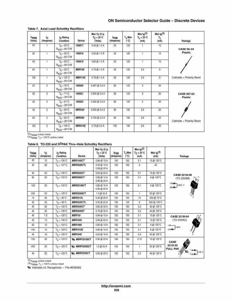
ON Semiconductor Selector Guide – Discrete Devices
http://onsemi.com 209
Table 7. Axial Lead Schottky Rectifiers
VRRM(Volts)
IO(Amperes)
IO RatingCondition Device
Max VF @ iFTC = 25°C
(Volts)IFSM
(Amperes)TJ Max
(°C)
Max IR(2)
TL = 25°C(mA)
Max IR(3)
TL(mA) Package
20 1 TA = 55°CRθJA = 80°C/W
1N5817 0.45 @ 1.0 A 25 125 1 10CASE 59–04
Pl i30 1 TA = 55°CRθJA = 80°C/W
1N5818 0.55 @ 1.0 A 25 125 1 10 Plastic
40 1 TA = 55°CRθJA = 80°C/W
1N5819 0.60 @ 1.0 A 25 125 1 10
60 1 TA = 55°CRθJA = 80°C/W
MBR160 0.75 @ 1.0 A 25 150 0.5 5
100 1 TA = 120°CRθJA = 50°C/W
MBR1100 0.79 @ 1.0 A 50 150 0.5 5 Cathode = Polarity Band
20 3 TA = 76°CRθJA = 28°C/W
1N5820 0.457 @ 3.0 A 80 125 2 20
30 3 TA = 71°CRθJA = 28°C/W
1N5821 0.500 @ 3.0 A 80 125 2 20 CASE 267-03Plastic
40 3 TA = 61°CRθJA = 28°C/W
1N5822 0.525 @ 3.0 A 80 125 2 20
40 3 TA = 65°CRθJA = 28°C/W
MBR340 0.600 @ 3.0 A 80 150 0.6 20
60 3 TA = 65°CRθJA = 28°C/W
MBR360 0.740 @ 3.0 A 80 150 0.6 20Cathode = Polarity Band
100 3 TA = 100°CRθJA = 28°C/W
MBR3100 0.79 @ 3.0 A 150 150 0.6 20
(2)VRRM unless noted(3)VRRM, TJ = 100°C unless noted
Table 8. TO-220 and D2PAK Thru–Hole Schottky Rectifiers
VRRM(Volts)
IO(Amperes)
IO RatingCondition Device
Max VF @ iFTC = 25°C
(Volts)IFSM
(Amperes)TJ Max
(°C)
Max IR(2)
TC = 25°C(mA)
Max IR(3)
(mA) Package
45 15 TC = 105°C MBR1545CT 0.84 @ 15 A 150 150 0.1 15 @ 125°C
30 20 TC = 137°C MBR2030CTL 0.52 @ 10 A0.58 @ 20 A
150 150 5 40
45 20 TC = 135°C MBR2045CT 0.84 @ 20 A 150 150 0.1 15 @ 125°CCASE 221A-09
60 20 TC = 133°C MBR2060CT 0.85 @ 10 A0.95 @ 20 A
150 150 0.1 6 @ 125°CCASE 221A-09
(TO-220AB)
1
4
100 20 TC = 133°C MBR20100CT 0.85 @ 10 A0.95 @ 20 A
150 150 0.1 6 @ 125°C1
32, 4
200 20 TC = 125°C MBR20200CT 1.0 @ 20 A 150 150 1 50 @ 125°C 1 2
15 25 TC = 90°C MBR2515L 0.45 @ 25 A 150 100 15 200 @ 70°C2
3
35 25 TC = 95°C MBR2535CTL 0.55 @ 25 A 150 125 5 500 @ 125°C
45 25 TC = 130°C MBR2545CT 0.82 @ 30 A 150 150 0.2 40 @ 125°C
45 30 TC = 130°C MBR3045ST 0.76 @ 30 A 150 150 0.2 40 @ 125°C
45 7.5 TC = 105°C MBR745 0.84 @ 15 A 150 150 0.1 15 @ 125°C CASE 221B-04 4
45 10 TC = 135°C MBR1045 0.84 @ 20 A 150 150 0.1 15 @ 125°C (TO-220AC)
60 10 TC = 133°C MBR1060 0.80 @ 10 A 150 150 0.1 6 @ 125°C 14
100 10 TC = 133°C MBR10100 0.80 @ 10 A 150 150 0.1 6 @ 125°C 13
4
45 16 TC = 125°C MBR1645 0.63 @ 16 A 150 150 0.2 40 @ 125°C 3
100 20 TC = 133°C MBRF20100CT 0.95 @ 20 A 150 150 0.15 15 @ 125°CCASE
200 20 TC = 125°C MBRF20200CT 1.0 @ 20 A 150 150 1 50 @ 125°C
11
221D-02FULL PAK
45 25 TC = 125°C MBRF2545CT 0.82 @ 25 A 150 150 0.2 40 @ 125°C12
33
2
Indicates UL Recognized — File #E69369
(2)VRRM unless noted(3)VRRM, TJ = 100°C unless noted

ON Semiconductor Selector Guide – Discrete Devices
http://onsemi.com 210
Table 9. TO-218 and TO-247 Schottky Rectifiers
VRRM(Volts)
IO(Amperes)
IO RatingCondition Device
Max VF @ iFTC = 25°C
(Volts)IFSM
(Amperes)TJ Max
(°C)
Max IR(2)
TC = 25°C(mA)
Max IR(3)
(mA) Package
45 30 TC = 105°C MBR3045PT 0.76 @ 30 A 200 150 1 100 @ 125°C CASE 4
45 40 TC = 125°C MBR4045PT 0.70 @ 20 A0.80 @ 40 A
400 150 1 50 340D-02(TO-218AC)
45 60 TC = 125°C MBR6045PT 0.62 @ 30 A0.75 @ 60 A
500 150 1 50 1
32
1
32, 4
45 30 TC = 105°C MBR3045WT 0.76 @ 30 A 200 150 1 100 @ 125°C
15 40 TC = 125°C MBR4015LWT 0.42 @ 20 A0.50 @ 40 A
400 150 5 150 @ 75°C
CASE 340K 0145 40 TC = 125°C MBR4045WT 0.70 @ 20 A
0.80 @ 40 A400 150 1 50
CASE 340K–01(TO-247)
145 60 TC = 125°C MBR6045WT 0.62 @ 30 A
0.75 @ 60 A500 150 1 50
1
321
32, 4
30 70 TC = 135°C MBR7030WT 0.55 @ 35 A0.70
400 150 5 250
(2)VRRM unless noted(3)VRRM, TJ = 100°C unless noted
Table 10. POWERTAP II Schottky Rectifiers
VRRM(Volts)
IO(1)
(Amperes)IO RatingCondition Device
Max VF @ iFTC = 25°C
(Volts)IFSM
(Amperes)TJ Max
(°C)
Max IR(2)TC = 25°C
(mA)Max IR(3)
(mA) Package
30 200 TC = 125°C MBRP20030CTL 0.52 @ 100 A0.60 @ 200 A
1500 150 5 —CASE 357C-03
35 600 TC = 100°C MBRP60035CTL 0.57 @ 300 A 4000 150 10 250 POWERTAP
45 200 TC = 125°C MBRP20045CT 0.78 @ 100 A 1500 175 0.5 50 @ 125°C 2
45 300 TC = 120°C MBRP30045CT 0.70 @ 150 A0.82 @ 300 A
2500 175 0.8 75 @ 125°C 1
45 400 TC = 100°C MBRP40045CTL 0.57 @ 200 A 2500 150 10 —1
60 200 TC = 125°C MBRP20060CT 0.800 @ 100 A 1500 175 0.5 50 @ 125°C 31
23
60 300 TC = 120°C MBRP30060CT 0.79 @ 150 A0.89 @ 300 A
2500 175 0.8 75 @ 125°C Cathode = Mounting PlateAnode = Terminal
100 400 TC = 100°C MBRP400100CTL 0.83 @ 200 A 2500 150 6 —(1)IO is total device current capability.(2)VRRM unless noted(3)VRRM, TJ = 100°C unless noted
Table 11. POWERTAP III Schottky Rectifiers
VRRM(Volts)
IO(1)
(Amperes)IO RatingCondition Device
Max VF @ iFTC = 25°C
(Volts)IFSM
(Amperes)TJ Max
(°C)
Max IR(2)TC = 25°C
(µA)
Max IR(3)
(µA)TJ = 100°C Package
35 200 TC = 100°C MBRP20035L 0.57 @ 200 A 2000 150 10 250 CASE 357D-01POWERTAP
1
300 TC = 100°C MBRP30035L 0.57 @ 300 A 3000 150 10 250
2
(1)IO is total device current capability.(2)VRRM unless noted(3)VRRM, TJ = 100°C unless noted
New Product
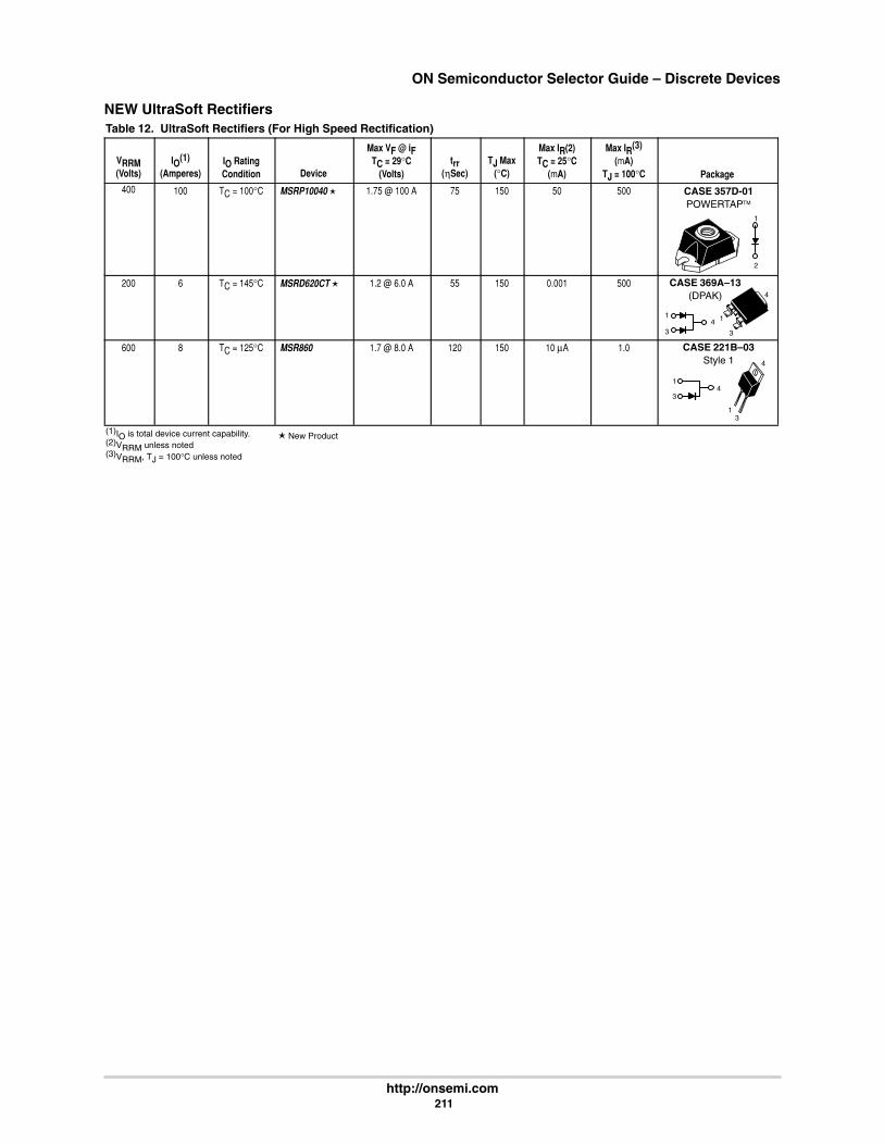
ON Semiconductor Selector Guide – Discrete Devices
http://onsemi.com 211
NEW UltraSoft RectifiersTable 12. UltraSoft Rectifiers (For High Speed Rectification)
VRRM(Volts)
IO(1)
(Amperes)IO RatingCondition Device
Max VF @ iFTC = 29°C
(Volts)trr
(ηSec)TJ Max
(°C)
Max IR(2)TC = 25°C
(mA)
Max IR(3)
(mA)TJ = 100°C Package
400 100 TC = 100°C MSRP10040 1.75 @ 100 A 75 150 50 500 CASE 357D-01POWERTAP
2
1
200 6 TC = 145°C MSRD620CT 1.2 @ 6.0 A 55 150 0.001 500 CASE 369A–13(DPAK)
3
1
3
4
41
600 8 TC = 125°C MSR860 1.7 @ 8.0 A 120 150 10 µA 1.0 CASE 221B–03Style 1
13
4
1
34
(1)IO is total device current capability.(2)VRRM unless noted(3)VRRM, TJ = 100°C unless noted
New Product
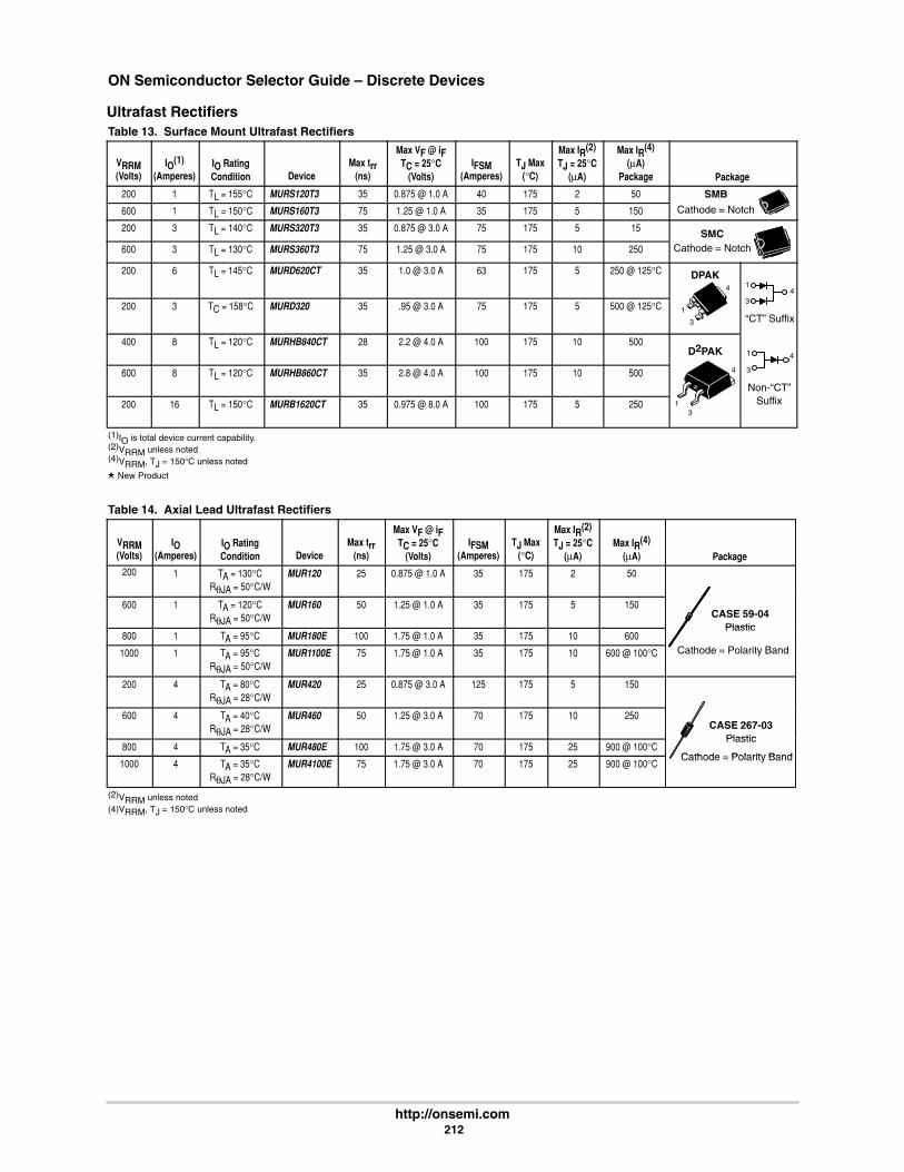
ON Semiconductor Selector Guide – Discrete Devices
http://onsemi.com 212
Ultrafast RectifiersTable 13. Surface Mount Ultrafast Rectifiers
VRRM(Volts)
IO(1)
(Amperes)IO RatingCondition Device
Max trr(ns)
Max VF @ iFTC = 25°C
(Volts)IFSM
(Amperes)TJ Max
(°C)
Max IR(2)
TJ = 25°C(µA)
Max IR(4)
(µA)Package Package
200 1 TL = 155°C MURS120T3 35 0.875 @ 1.0 A 40 175 2 50 SMB
600 1 TL = 150°C MURS160T3 75 1.25 @ 1.0 A 35 175 5 150 Cathode = Notch
200 3 TL = 140°C MURS320T3 35 0.875 @ 3.0 A 75 175 5 15 SMC
600 3 TL = 130°C MURS360T3 75 1.25 @ 3.0 A 75 175 10 250 Cathode = Notch
200 6 TL = 145°C MURD620CT 35 1.0 @ 3.0 A 63 175 5 250 @ 125°C DPAK4 1
4
200 3 TC = 158°C MURD320 35 .95 @ 3.0 A 75 175 5 500 @ 125°C3
1“CT” Suffix
3
400 8 TL = 120°C MURHB840CT 28 2.2 @ 4.0 A 100 175 10 500D2PAK 41
600 8 TL = 120°C MURHB860CT 35 2.8 @ 4.0 A 100 175 10 500 4
Non-“CT”
3
200 16 TL = 150°C MURB1620CT 35 0.975 @ 8.0 A 100 175 5 2503
1 Suffix
(1)IO is total device current capability.(2)VRRM unless noted(4)VRRM, TJ = 150°C unless noted
New Product
Table 14. Axial Lead Ultrafast Rectifiers
VRRM(Volts)
IO(Amperes)
IO RatingCondition Device
Max trr(ns)
Max VF @ iFTC = 25°C
(Volts)IFSM
(Amperes)TJ Max
(°C)
Max IR(2)
TJ = 25°C(µA)
Max IR(4)
(µA) Package
200 1 TA = 130°CRθJA = 50°C/W
MUR120 25 0.875 @ 1.0 A 35 175 2 50
600 1 TA = 120°CRθJA = 50°C/W
MUR160 50 1.25 @ 1.0 A 35 175 5 150CASE 59-04
Plastic800 1 TA = 95°C MUR180E 100 1.75 @ 1.0 A 35 175 10 600
Plastic
1000 1 TA = 95°CRθJA = 50°C/W
MUR1100E 75 1.75 @ 1.0 A 35 175 10 600 @ 100°C Cathode = Polarity Band
200 4 TA = 80°CRθJA = 28°C/W
MUR420 25 0.875 @ 3.0 A 125 175 5 150
600 4 TA = 40°CRθJA = 28°C/W
MUR460 50 1.25 @ 3.0 A 70 175 10 250CASE 267-03
Plastic800 4 TA = 35°C MUR480E 100 1.75 @ 3.0 A 70 175 25 900 @ 100°C
Plastic
Cathode Polarity Band1000 4 TA = 35°C
RθJA = 28°C/WMUR4100E 75 1.75 @ 3.0 A 70 175 25 900 @ 100°C
Cathode = Polarity Band
(2)VRRM unless noted(4)VRRM, TJ = 150°C unless noted

ON Semiconductor Selector Guide – Discrete Devices
http://onsemi.com 213
Table 15. TO-220 Ultrafast and MEGAHERTZ Rectifiers
VRRM(Volts)
IO(1)
(Amperes)IO RatingCondition Device
Max trr(ns)
Max VF @ iFTC = 25°C
(Volts)IFSM
(Amperes)TJ Max
(°C)
Max IR(2)
TC = 25°C(µA)
Max IR(4)
(µA) Package
200 6 TC = 130°C MUR620CT 35 0.975 @ 3.0 A 75 175 5 250 CASE 221A-09(TO 220AB)
400 8 TC = 120°C MURH840CT 28 2.0 @ 4.0 A 100 175 10 500(TO-220AB)
1
4
600 8 TC = 120°C MURH860CT 35 2.8 @ 4.0 A 100 175 10 5001
32, 4
200 16 TC = 150°C MUR1620CT 35 0.975 @ 8.0 A 100 175 5 2501
12
200 16 TC = 160°C MUR1620CTR 85 1.2 @ 8.0 A 100 175 5 5001
32, 4
23
400 16 TC = 150°C MUR1640CT 60 1.30 @ 8.0 A 100 175 10 2503
MUR1620CTR600 16 TC = 150°C MUR1660CT 60 1.5 @ 8.0 A 100 175 10 500
MUR1620CTROnly
200 8 TC = 150°C MUR820 35 0.975 @ 8.0 A 100 175 5 250
400 8 TC = 150°C MUR840 50 1.30 @ 8.0 A 100 175 10 500
600 8 TC = 150°C MUR860 50 1.50 @ 8.0 A 100 175 10 500
800 8 TC = 175°C MUR880E 75 1.80 @ 8.0 A 100 175 25 500 @ 100°C CASE 221B-04(TO 220AC)
1000 8 TC = 150°C MUR8100E 75 1.80 @ 8.0 A 100 175 25 500 @ 100°C(TO-220AC) 4
1200 10 TC = 125°C MUR10120E 175 2.2 @ 6.5 A 100 125 100 1000 @ 125°C 14
1500 10 TC = 125°C MUR10150E 175 2.4 @ 6.5 A 100 125 100 1000 @ 125°C 34
1500 5 TC = 100°C MUR5150E 175 2.4 @ 5 A 100 125 50 500 @ 125°C 13
200 15 TC = 150°C MUR1520 35 1.05 @ 15 A 200 175 10 500
400 15 TC = 150°C MUR1540 60 1.25 @ 15 A 150 175 10 500
600 15 TC = 145°C MUR1560 60 1.50 @ 15 A 150 175 10 1000
200 16 TC = 150°C MURF1620CT 25 0.975 @ 8.0 A 100 150 5 250CASE 221D-02
600 8 TC
120°C MURHF860CT 35 2.8 @ 4.0 A 100 175 10 500
(1)IO is total device capability(2)VRRM unless noted(4)VRRM, TJ = 150°C unless noted
Indicates UL Recognized — File #E69369 New Product
Table 16. TO-218 and TO-247 Ultrafast Rectifiers
VRRM(Volts)
IO(Amperes)
IO RatingCondition Device
Max trr(ns)
Max VF @ iFTC = 25°C
(Volts)IFSM
(Amperes)TJ Max
(°C)
Max IR(2)
TJ = 25°C(µA)
Max IR(4)
(mA) Package
200 30 TC = 145°C MUR3020WT 35 1.05 @ 15 A 150 175 10 0.5CASE 340K–01
(TO-247)1
2 4
600 30 TC = 145°C MUR3060WT 60 1.70 @ 15 A 150 175 10 13
2, 4
13
2
200 30 TC = 150°C MUR3020PT 35 1.12 @ 15 A 200 175 10 0.5 CASE 340D-02(TO-218AC) 4
400 30 TC = 150°C MUR3040PT 60 1.12 @ 15 A 150 175 10 0.5
(TO 218AC)
1
32, 4
4
600 30 TC = 145°C MUR3060PT 60 1.20 @ 15 A 150 175 10 13
1
32
400 30 TC = 70°C MUR3040 100 1.5 @ 30 A 300 175 35 6 @ 100°C CASE 340E-02(TO-218) 4
800 30 TC = 70°C MUR3080 110 1.90 @ 30 A 300 175 100 5 @ 100°C
(TO 218)1
34
4
400 60 TC = 70°C MUR6040 100 1.50 @ 60 A 600 175 60 10 @ 100°C
3
1
3
(1)IO is total device capability(2)VRRM unless noted(4)VRRM, TJ = 150°C unless noted
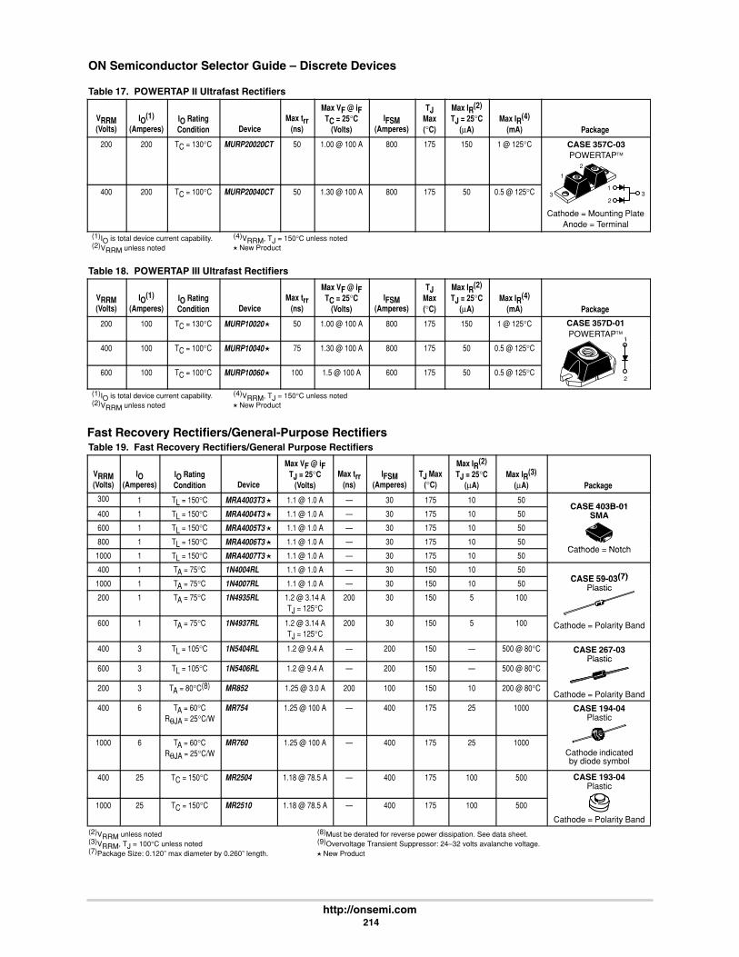
ON Semiconductor Selector Guide – Discrete Devices
http://onsemi.com 214
Table 17. POWERTAP II Ultrafast Rectifiers
VRRM(Volts)
IO(1)
(Amperes)IO RatingCondition Device
Max trr(ns)
Max VF @ iFTC = 25°C
(Volts)IFSM
(Amperes)
TJMax(°C)
Max IR(2)
TJ = 25°C(µA)
Max IR(4)
(mA) Package
200 200 TC = 130°C MURP20020CT 50 1.00 @ 100 A 800 175 150 1 @ 125°C CASE 357C-03POWERTAP
1
2
400 200 TC = 100°C MURP20040CT 50 1.30 @ 100 A 800 175 50 0.5 @ 125°C
Cathode = Mounting PlateAnode = Terminal
31
23
(1)IO is total device current capability.(2)VRRM unless noted New Product
(4)VRRM, TJ = 150°C unless noted
Table 18. POWERTAP III Ultrafast Rectifiers
VRRM(Volts)
IO(1)
(Amperes)IO RatingCondition Device
Max trr(ns)
Max VF @ iFTC = 25°C
(Volts)IFSM
(Amperes)
TJMax(°C)
Max IR(2)
TJ = 25°C(µA)
Max IR(4)
(mA) Package
200 100 TC = 130°C MURP10020 50 1.00 @ 100 A 800 175 150 1 @ 125°C CASE 357D-01POWERTAP
1
400 100 TC = 100°C MURP10040 75 1.30 @ 100 A 800 175 50 0.5 @ 125°C1
600 100 TC = 100°C MURP10060 100 1.5 @ 100 A 600 175 50 0.5 @ 125°C2
(1)IO is total device current capability.(2)VRRM unless noted New Product
(4)VRRM, TJ = 150°C unless noted
Fast Recovery Rectifiers/General-Purpose RectifiersTable 19. Fast Recovery Rectifiers/General Purpose Rectifiers
VRRM(Volts)
IO(Amperes)
IO RatingCondition Device
Max VF @ iFTJ = 25°C
(Volts)Max trr
(ns)IFSM
(Amperes)TJ Max
(°C)
Max IR(2)
TJ = 25°C(µA)
Max IR(3)
(µA) Package
300 1 TL = 150°C MRA4003T3 1.1 @ 1.0 A — 30 175 10 50CASE 403B-01
400 1 TL = 150°C MRA4004T3 1.1 @ 1.0 A — 30 175 10 50CASE 403B-01
SMA600 1 TL = 150°C MRA4005T3 1.1 @ 1.0 A — 30 175 10 50
800 1 TL = 150°C MRA4006T3 1.1 @ 1.0 A — 30 175 10 50Cathode Notch
1000 1 TL = 150°C MRA4007T3 1.1 @ 1.0 A — 30 175 10 50Cathode = Notch
400 1 TA = 75°C 1N4004RL 1.1 @ 1.0 A — 30 150 10 50CASE 59 03(7)
1000 1 TA = 75°C 1N4007RL 1.1 @ 1.0 A — 30 150 10 50 CASE 59-03(7)Plastic
200 1 TA = 75°C 1N4935RL 1.2 @ 3.14 ATJ = 125°C
200 30 150 5 100Plastic
600 1 TA = 75°C 1N4937RL 1.2 @ 3.14 ATJ = 125°C
200 30 150 5 100 Cathode = Polarity Band
400 3 TL = 105°C 1N5404RL 1.2 @ 9.4 A — 200 150 — 500 @ 80°C CASE 267-03Plastic
600 3 TL = 105°C 1N5406RL 1.2 @ 9.4 A — 200 150 — 500 @ 80°CPlastic
200 3 TA = 80°C(8) MR852 1.25 @ 3.0 A 200 100 150 10 200 @ 80°CCathode = Polarity Band
400 6 TA = 60°CRθJA = 25°C/W
MR754 1.25 @ 100 A — 400 175 25 1000 CASE 194-04Plastic
1000 6 TA = 60°CRθJA = 25°C/W
MR760 1.25 @ 100 A — 400 175 25 1000Cathode indicatedby diode symbol
400 25 TC = 150°C MR2504 1.18 @ 78.5 A — 400 175 100 500 CASE 193-04Plastic
1000 25 TC = 150°C MR2510 1.18 @ 78.5 A — 400 175 100 500
Cathode = Polarity Band(2)VRRM unless noted(3)VRRM, TJ = 100°C unless noted(7)Package Size: 0.120” max diameter by 0.260” length.
(8)Must be derated for reverse power dissipation. See data sheet.(9)Overvoltage Transient Suppressor: 24–32 volts avalanche voltage. New Product
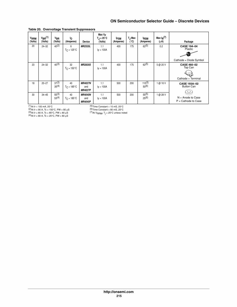
ON Semiconductor Selector Guide – Discrete Devices
http://onsemi.com 215
Table 20. Overvoltage Transient Suppressors
VRRM(Volts)
VBR(1)
(Volts)VBR
(Volts)IO
(Amperes) Device
Max VFTJ = 25°C
(Volts)IFSM
(Amperes)TJ Max
(°C)IRSM
(Amperes)Max IR(7)
(µA) Package
20 24–32 40(2) 6TC = 125°C
MR2535L 1.1IF = 100A
400 175 62(5) 0.2 CASE 194–04
Cathode = Diode Symbol
Plastic
23 24–32 40(3) 32TC = 150°C
MR2835S 1.1IF = 100A
400 175 62(5) 5 @ 20 V CASE 460–02
Cathode = Terminal
Top Can
18 20–27 37(3)
35(4)40
TC = 185°CMR4027N
andMR4027P
1.1IF = 100A
500 200 110(5)
50(6)1 @ 16 V CASE 193A–02
Button Can
30 34–45 55(3)
53(4)40
TC = 185°CMR4045N
andMR4045P
1.1IF = 100A
500 200 55(5)
25(6)1 @ 28 V
N = Anode to CaseP = Cathode to Case
(1)At Ir = 100 mA, 25°C(2)At Ir = 90 A, Tc = 150°C, PW = 80 µS(3)At Ir = 80 A, Tc = 85°C, PW = 80 µS(4)At Ir = 80 A, Tc = 25°C, PW = 80 µS
(5)Time Constant = 10 mS, 25°C(6)Time Constant = 80 mS, 25°C(7)At VRRM, Tj = 25°C unless noted

ON Semiconductor Selector Guide – Discrete Devices
http://onsemi.com 216
Thyristors, Triggers and Surge Suppressors
In Brief . . .Page
Silicon Controlled Rectifiers 217. . . . . . . . . . . . . . . . . . . . TRIACs 222. . . . . . . . . . . . . . . . . . . . . . . . . . . . . . . . . . . . . Thyristor Triggers 233. . . . . . . . . . . . . . . . . . . . . . . . . . . . .
Programmable UnijunctionTransistors — PUT 233. . . . . . . . . . . . . . . . . . . . . . . .
Thyristor Surge Suppressors 233. . . . . . . . . . . . . . . . . . . SIDAC’s 233. . . . . . . . . . . . . . . . . . . . . . . . . . . . . . . . . . High Voltage Bidirectional Surge ProtectorDevices (SIDAC’s) 233. . . . . . . . . . . . . . . . . . . . . . . .
ON Semiconductor’s broad line of Thyristorsincludes. . . .• A full line of TRIACs and SCRs covering a forward
current range from 0.6 to 55 amperes and blockingvoltages from 30 to 800 volts.
• Plastic package for lowest cost which includes thefully insulated plastic Case 221C (TO–220 Isolated).Then there are the special applications devices for
Ignition circuits and Crowbar applications. Also includedare isolated packaged devices for appliances and surfacemount packages for surface mounting in space–savingrequirements.
New in the ON Semiconductor Thyristor line–up arethe high–performance TO–220 TRIACs, such as theMAC8 and MAC12 series designed specifically forwhite goods and motor control applications.

I (–)
V (–) V (+)IRRM VDRM
REVERSEBLOCKINGREGION
REVERSEAVALANCHE REGION
FORWARDBREAKOVERPOINT
FORWARDBLOCKINGREGION
IHIDRMVRRM
IT
I (+)
VT
ON Semiconductor Selector Guide – Discrete Devices
http://onsemi.com 217
SCRs
SiliconControlledRectifiers
Table 1. SCRs — General Purpose Plastic Packages0.8 to 55 Amperes RMS, 30 to 800 Volts
On–State (RMS) Current
0.8 AMP 1.5 AMPS
TC = 58°C TC = 80°C TC = 50°C
KG A
K
GA
A
KG A
VDRMSensitive GateVDRM
VRRM(Volts)
Case 29–11TO–226AA (TO–92) Style 10
Case 318ESOT–223 STYLE 10
Case 29–11TO–226AA (TO–92)
Style 10
30 2N5060 (1) — —
60 2N5061 (1) — —
100 2N5062 (1)
MCR100–3 (1)——
——
200 2N5064 (1)
MCR100–4 (1)MCR08BT1
———
400 MCR100–6 (1) — MCR22–6 (1)
600 MCR100–8 (1) MCR08MT1 MCR22–8 (1)
Maximum Electrical Characteristics
ITSM (Amps)60 Hz
10 10 15(1)150(3)
IGT (mA) 0.2
VGT (V) 0.8
TJ OperatingRange (°C)
–65 to+110
–40 to+110
–40 to+125
(1) RLRA, RLRE, RL, RL1 Suffix: Radial Tape and ReelRLRM, ZL1 Suffix: Radial Tape and Ammo Pack
(3) Exponential decay 2 µs wide at 5 time constants, f = 12 Hz
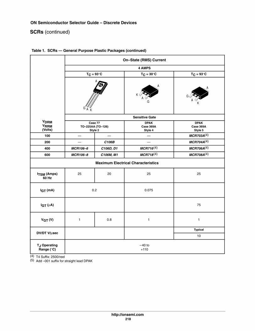
ON Semiconductor Selector Guide – Discrete Devices
http://onsemi.com 218
SCRs (continued)
Table 1. SCRs — General Purpose Plastic Packages (continued)
On–State (RMS) Current
4 AMPS
TC = 93°C TC = 30°C TC = 93°C
G A K
AA
K
GA
K
GA
A
VSensitive Gate
VDRMVRRM(Volts)
Case 77TO–225AA (TO–126)
Style 2
DPAKCase 369A
Style 4
DPAKCase 369A
Style 5
100 — — — MCR703A(4)
200 — C106B — MCR704A(4)
400 MCR106–6 C106D, D1 MCR716 (4) MCR706A(4)
600 MCR106–8 C106M, M1 MCR718 (4) MCR708A(4)
Maximum Electrical Characteristics
ITSM (Amps)60 Hz
25 20 25 25
IGT (mA) 0.2 0.075
IGT (µA) 75
VGT (V) 1 0.8 1 1
DV/DT V/µsecTypical
DV/DT V/µsec10
TJ OperatingRange (°C)
–40 to+110
(4) T4 Suffix: 2500/reel(5) Add –001 suffix for straight lead DPAK
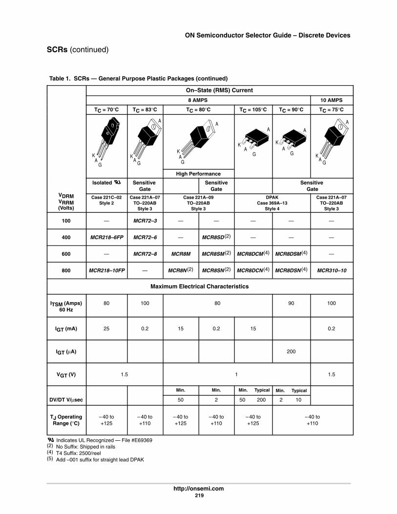
ON Semiconductor Selector Guide – Discrete Devices
http://onsemi.com 219
SCRs (continued)
Table 1. SCRs — General Purpose Plastic Packages (continued)
On–State (RMS) Current
8 AMPS 10 AMPS
TC = 70°C TC = 83°C TC = 80°C TC = 105°C TC = 90°C TC = 75°C
KA
G
KA
G
A
KAG
A
K
A
GA
K
G
A
AK
AG
A
High Performance
V
Isolated Sensitive Gate
SensitiveGate
Sensitive Gate
VDRMVRRM(Volts)
Case 221C–02Style 2
Case 221A–07TO–220AB
Style 3
Case 221A–09TO–220AB
Style 3
DPAKCase 369A–13
Style 4
Case 221A–07TO–220AB
Style 3
100 — MCR72–3 — — — — —
400 MCR218–6FP MCR72–6 — MCR8SD (2) — — —
600 — MCR72–8 MCR8M MCR8SM (2) MCR8DCM(4) MCR8DSM(4) —
800 MCR218–10FP — MCR8N (2) MCR8SN (2) MCR8DCN (4) MCR8DSN (4) MCR310–10
Maximum Electrical Characteristics
ITSM (Amps)60 Hz
80 100 80 90 100
IGT (mA) 25 0.2 15 0.2 15 0.2
IGT (µA) 200
VGT (V) 1.5 1 1.5
Min. Min. Min. Typical Min. Typical
DV/DT V/µsec 50 2 50 200 2 10
TJ OperatingRange (°C)
–40 to+125
–40 to+110
–40 to+125
–40 to+110
–40 to+125
–40 to+110
Indicates UL Recognized — File #E69369(2) No Suffix: Shipped in rails(4) T4 Suffix: 2500/reel(5) Add –001 suffix for straight lead DPAK
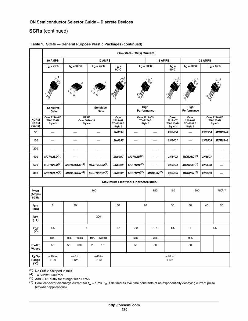
ON Semiconductor Selector Guide – Discrete Devices
http://onsemi.com 220
SCRs (continued)
Table 1. SCRs — General Purpose Plastic Packages (continued)
On–State (RMS) Current
10 AMPS 12 AMPS 16 AMPS 25 AMPS
TC = 75°C TC = 90°C TC = 75°C TC =90°C
TC = 80°C TC =90°C
TC = 80°C TC = 85°C
KAG
A
K
A
GA K
A
GA K
AG
A
KA
G
A
KAG
A
KAG
A
KAG
A
Sensitive Gate
Sensitive Gate
High Performance
HighPerformance
VDRMVRRM(Volts)
Case 221A–07TO–220AB
Style 3
DPAKCase 369A–13
Style 4
Case221A–07
TO–220ABStyle 3
Case 221A–09TO–220AB
Style 3
Case221A–07
TO–220ABStyle 3
Case221A–09
TO–220ABStyle 3
Case 221A–07TO–220AB
Style 3
50 — — — 2N6394 — — 2N6400 — 2N6504 MCR69–2
100 — — — 2N6395 — — 2N6401 — 2N6505 MCR69–3
200 — — — — — — — — — —
400 MCR12LD (2) — — 2N6397 MCR12D (2) — 2N6403 MCR25D (2) 2N6507 —
600 MCR12LM (2) MCR12DCM (4) MCR12DSM (4) 2N6398 MCR12M (2) — 2N6404 MCR25M (2) 2N6508 —
800 MCR12LN (2) MCR12DCN (4) MCR12DSN (4) 2N6399 MCR12N ( 2) MCR16N (2) 2N6405 MCR25N (2) 2N6509 —
Maximum Electrical Characteristics
ITSM(Amps)60 Hz
100 150 160 300 750(7)
IGT(mA)
8 20 30 20 30 30 40 30
IGT(µA)
200
VGT(V)
1.5 1 1.5 2.2 1.7 1.5 1 1.5
Min. Min. Typical Min. Typical Min. Min. Min.
DV/DTV/µsec
50 50 200 2 10 50 50 50
TJ OpRange
(°C)
– 40 to+100
– 40 to+125
– 40 to+110
– 40 to+125
(2) No Suffix: Shipped in rails(4) T4 Suffix: 2500/reel(5) Add –001 suffix for straight lead DPAK(7) Peak capacitor discharge current for tw = 1 ms. tw is defined as five time constants of an exponentially decaying current pulse
(crowbar applications).

ON Semiconductor Selector Guide – Discrete Devices
http://onsemi.com 221
SCRs (continued)
Table 1. SCRs — General Purpose Plastic Packages (continued)
On–State (RMS) Current
25 AMPS 40 AMPS 55 AMPS
TC = 85°C TC = 80°C TC = 70°C
KA
G KA
G
A
VIsolated
AG
VDRMVRRM(Volts)
Case 221C–02Style 2
Case 221A–07TO–220AB
Style 3
200 — MCR264–4 MCR265–4
400 — MCR264–6 MCR265–6
600 MCR225–8FP MCR264–8 MCR265–8
800 MCR225–10FP — MCR265–10
Maximum Electrical Characteristics
ITSM (Amps)60 Hz
(1
300400 550
IGT (mA) 40 50
VGT (V) 1.5
TJ OperatingRange (°C)
–40 to+125
Indicates UL Recognized — File #E69369
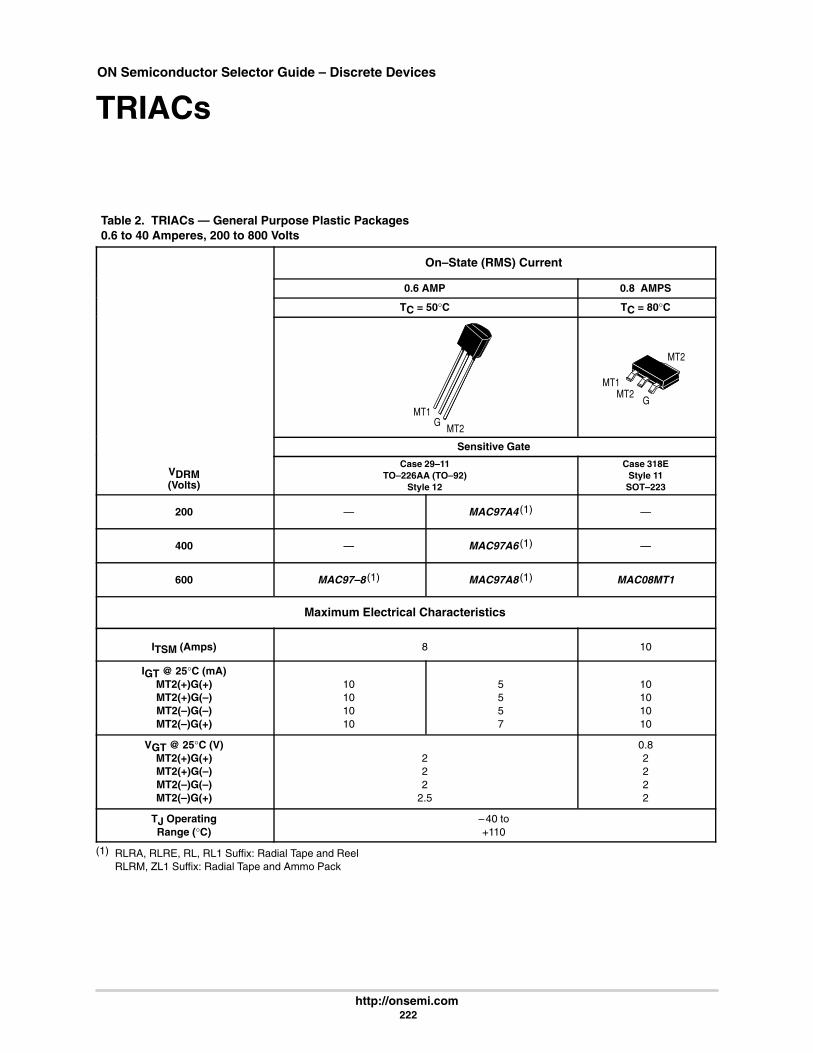
ON Semiconductor Selector Guide – Discrete Devices
http://onsemi.com 222
TRIACs
Table 2. TRIACs — General Purpose Plastic Packages0.6 to 40 Amperes, 200 to 800 Volts
On–State (RMS) Current
0.6 AMP 0.8 AMPS
TC = 50°C TC = 80°C
MT1G
MT2
MT1
GMT2
MT2
Sensitive Gate
VDRM(Volts)
Case 29–11TO–226AA (TO–92)
Style 12
Case 318EStyle 11
SOT–223
200 — MAC97A4 (1) —
400 — MAC97A6 (1) —
600 MAC97–8 (1) MAC97A8 (1) MAC08MT1
Maximum Electrical Characteristics
ITSM (Amps) 8 10
IGT @ 25°C (mA)MT2(+)G(+)MT2(+)G(–)MT2(–)G(–)MT2(–)G(+)
10101010
5557
10101010
VGT @ 25°C (V)MT2(+)G(+)MT2(+)G(–)MT2(–)G(–)MT2(–)G(+)
222
2.5
0.82222
TJ OperatingRange (°C)
–40 to+110
(1) RLRA, RLRE, RL, RL1 Suffix: Radial Tape and ReelRLRM, ZL1 Suffix: Radial Tape and Ammo Pack
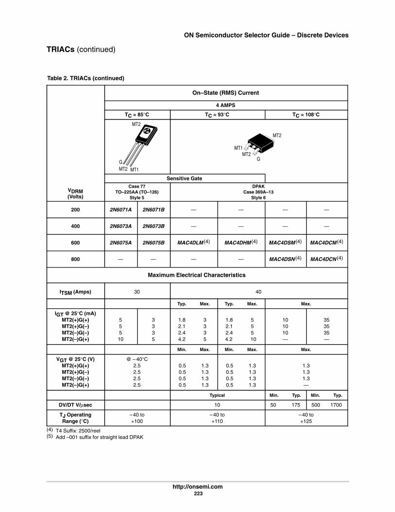
ON Semiconductor Selector Guide – Discrete Devices
http://onsemi.com 223
TRIACs (continued)
Table 2. TRIACs (continued)
On–State (RMS) Current
4 AMPS
TC = 85°C TC = 93°C TC = 108°C
GMT2 MT1
MT2
G
MT2
MT1MT2
Sensitive Gate
VDRM(Volts)
Case 77TO–225AA (TO–126)
Style 5
DPAKCase 369A–13
Style 6
200 2N6071A 2N6071B — — — —
400 2N6073A 2N6073B — — — —
600 2N6075A 2N6075B MAC4DLM (4) MAC4DHM (4) MAC4DSM (4) MAC4DCM (4)
800 — — — — MAC4DSN (4) MAC4DCN (4)
Maximum Electrical Characteristics
ITSM (Amps) 30 40
Typ. Max. Typ. Max. Max.
IGT @ 25°C (mA)MT2(+)G(+)MT2(+)G(–)MT2(–)G(–)MT2(–)G(+)
55510
3335
1.8 32.1 32.4 34.2 5
1.8 52.1 52.4 54.2 10
101010—
353535—
Min. Max. Min. Max. Max.
VGT @ 25°C (V)MT2(+)G(+)MT2(+)G(–)MT2(–)G(–)MT2(–)G(+)
@ –40°C2.52.52.52.5
0.5 1.30.5 1.30.5 1.30.5 1.3
0.5 1.30.5 1.30.5 1.30.5 1.3
1.31.31.3—
Typical Min. Typ. Min. Typ.
DV/DT V/µsec 10 50 175 500 1700
TJ OperatingRange (°C)
–40 to+100
–40 to+110
–40 to+125
(4) T4 Suffix: 2500/reel(5) Add –001 suffix for straight lead DPAK

ON Semiconductor Selector Guide – Discrete Devices
http://onsemi.com 224
TRIACs (continued)
Table 2. TRIACs (continued)
On–State (RMS) Current
4 AMPS 6 AMPS
TC = 100°C TC = 80°C
MT1MT2
G
MT2
VDRM(Volts)
Case 221A–07TO–220AB
Style 4
200 — — —
400 — — T2500D
600 MAC4SM MAC4M —
800 MAC4SN MAC4N —
Maximum Electrical Characteristics
ITSM (Amps) 40 60
IGT @ 25°C (mA)MT2(+)G(+)MT2(+)G(–)MT2(–)G(–)MT2(–)G(+)
101010—
353535—
25602560
VGT @ 25°C (V)MT2(+)G(+)MT2(+)G(–)MT2(–)G(–)MT2(–)G(+)
1.31.31.3(—
2.52.52.52.5
TJ OperatingRange (°C)
–40 to +125 –40 to 100
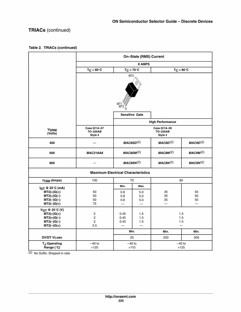
ON Semiconductor Selector Guide – Discrete Devices
http://onsemi.com 225
TRIACs (continued)
Table 2. TRIACs (continued)
On–State (RMS) Current
8 AMPS
TC = 80°C TC = 70°C TC = 80°C
MT1MT2
G
MT2
Sensitive Gate
High Performance
VDRM(Volts)
Case 221A–07TO–220AB
Style 4
Case 221A–09TO–220AB
Style 4
400 — MAC8SD (2) MAC8D (2) MAC9D (2)
600 MAC218A8 MAC8SM (2) MAC8M (2) MAC9M (2)
800 — MAC8SN (2) MAC8N (2) MAC9N (2)
Maximum Electrical Characteristics
ITSM (Amps) 100 70 80
IGT @ 25°C (mA)Min. Max.
IGT @ 25 C (mA)MT2(+)G(+)MT2(+)G(–)MT2(–)G(–)MT2(–)G(+)
50505075
0.80.80.8—
5.05.05.0—
353535—
505050—
VGT @ 25°C (V)MT2(+)G(+)MT2(+)G(–)MT2(–)G(–)MT2(–)G(+)
222
2.5
0.450.450.45—
1.51.51.5—
1.51.51.5—
Min. Min. Min.
DV/DT V/µsec 25 250 500
TJ OperatingRange (°C)
–40 to+125
–40 to+110
–40 to+125
(2) No Suffix: Shipped in rails
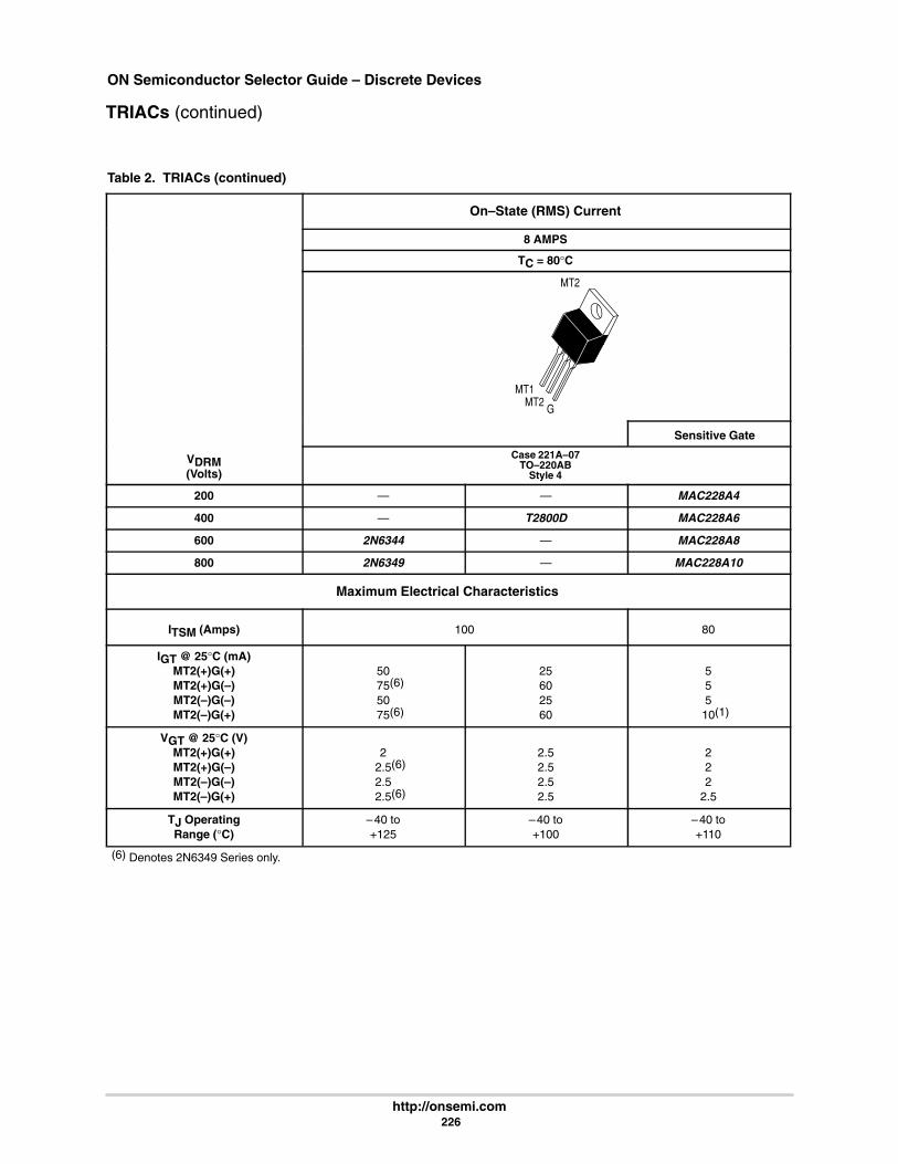
ON Semiconductor Selector Guide – Discrete Devices
http://onsemi.com 226
TRIACs (continued)
Table 2. TRIACs (continued)
On–State (RMS) Current
8 AMPS
TC = 80°C
MT2
MT1MT2
G
Sensitive Gate
VDRM(Volts)
Case 221A–07TO–220AB
Style 4
200 — — MAC228A4
400 — T2800D MAC228A6
600 2N6344 — MAC228A8
800 2N6349 — MAC228A10
Maximum Electrical Characteristics
ITSM (Amps) 100 80
IGT @ 25°C (mA)MT2(+)G(+)MT2(+)G(–)MT2(–)G(–)MT2(–)G(+)
50(6)75(6)
50(6)75(6)
25602560
555
(1)10(1)
VGT @ 25°C (V)MT2(+)G(+)MT2(+)G(–)MT2(–)G(–)MT2(–)G(+)
2(6)2.5(6)
2.5(6)2.5(6)
2.52.52.52.5
222
2.5
TJ OperatingRange (°C)
–40 to+125
–40 to+100
–40 to+110
(6) Denotes 2N6349 Series only.
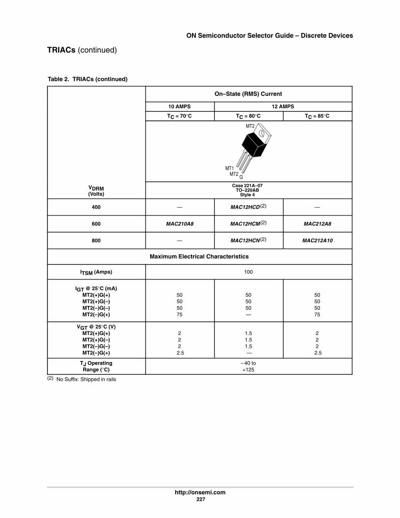
ON Semiconductor Selector Guide – Discrete Devices
http://onsemi.com 227
TRIACs (continued)
Table 2. TRIACs (continued)
On–State (RMS) Current
10 AMPS 12 AMPS
TC = 70°C TC = 80°C TC = 85°C
MT1MT2
G
MT2
VDRM(Volts)
Case 221A–07TO–220AB
Style 4
400 — MAC12HCD (2) —
600 MAC210A8 MAC12HCM (2) MAC212A8
800 — MAC12HCN (2) MAC212A10
Maximum Electrical Characteristics
ITSM (Amps) 100
IGT @ 25°C (mA)MT2(+)G(+)MT2(+)G(–)MT2(–)G(–)MT2(–)G(+)
50505075
505050—
50505075
VGT @ 25°C (V)MT2(+)G(+)MT2(+)G(–)MT2(–)G(–)MT2(–)G(+)
222
(2.5
1.51.51.5(—
222
(2.5
TJ OperatingRange (°C)
–40 to+125
(2) No Suffix: Shipped in rails

ON Semiconductor Selector Guide – Discrete Devices
http://onsemi.com 228
TRIACs (continued)
Table 2. TRIACs (continued)
On–State (RMS) Current
12 AMPS 15 AMPS
TC = 80°C TC = 70°C TC = 90°C TC = 80°C
MT1MT2
G
MT2
Sensitive Gate
High PerformanceHigh
Performance
VDRM(Volts)
Case 221A–07TO–220AB
Style 4
Case 221A–09TO–220AB
Style 4
Case 221A–07TO–220AB
Style 4
Case 221A–09TO–220AB
Style 4
400 — MAC12D (2) — — MAC15A6 MAC16D (2)
600 2N6348A MAC12M (2) MAC15M (2) MAC15SM (2) MAC15A8 MAC16M (2)
800 — MAC12N (2) MAC15N (2) MAC15SN (2) MAC15A10 MAC16N (2)
Maximum Electrical Characteristics
ITSM (Amps) 120 150 120 150
IGT @ 25°C (mA)Min. Max.
IGT @ 25 C (mA)MT2(+)G(+)MT2(+)G(–)MT2(–)G(–)MT2(–)G(+)
50755075
353535—
0.80.80.8—
5.05.05.0—
50505075
505050—
VGT @ 25°C (V)MT2(+)G(+)MT2(+)G(–)MT2(–)G(–)MT2(–)G(+)
22.52
2.5
1.51.51.5—
0.450.450.45—
1.51.51.5—
222
2.5
1.51.51.5—
Min. Min. Min. Min.
DV/DT V/µsec 250 250 25 500
TJ OperatingRange (°C)
–40 to+125
–40 to+110
–40 to+125
(2) No Suffix: Shipped in rails
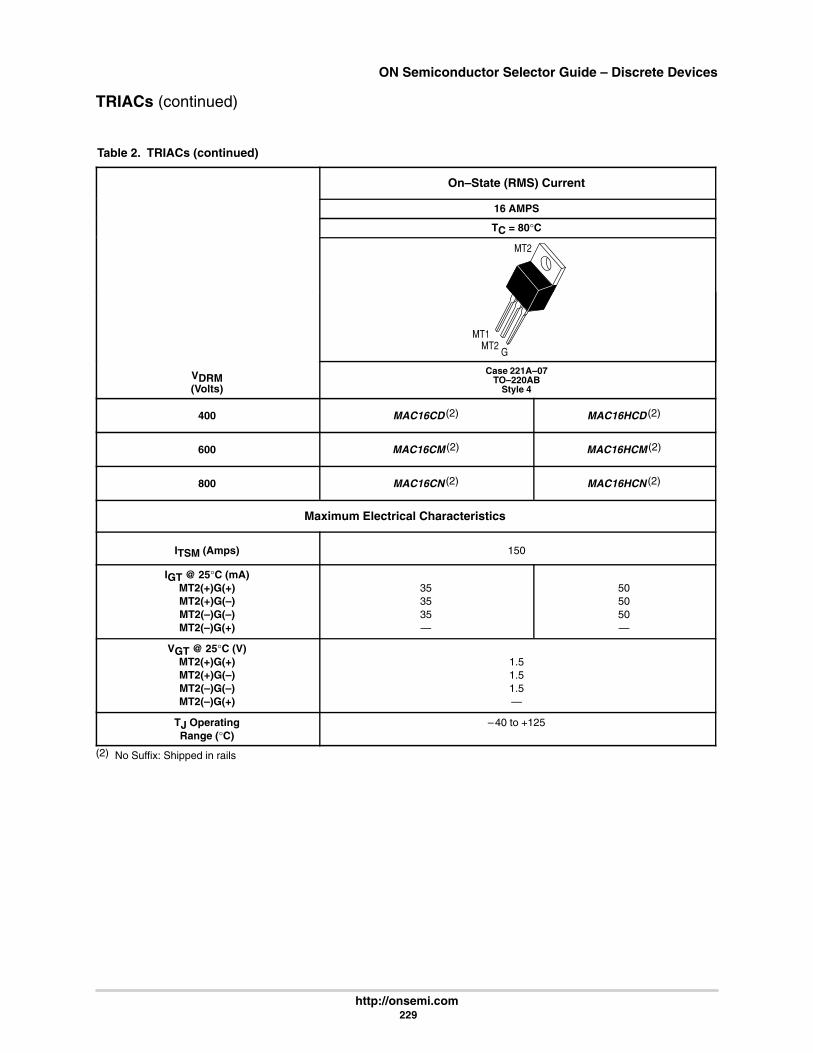
ON Semiconductor Selector Guide – Discrete Devices
http://onsemi.com 229
TRIACs (continued)
Table 2. TRIACs (continued)
On–State (RMS) Current
16 AMPS
TC = 80°C
MT2
MT1MT2
G
VDRM(Volts)
Case 221A–07TO–220AB
Style 4
400 MAC16CD (2) MAC16HCD (2)
600 MAC16CM (2) MAC16HCM (2)
800 MAC16CN (2) MAC16HCN (2)
Maximum Electrical Characteristics
ITSM (Amps) 150
IGT @ 25°C (mA)MT2(+)G(+)MT2(+)G(–)MT2(–)G(–)MT2(–)G(+)
353535—
505050—
VGT @ 25°C (V)MT2(+)G(+)MT2(+)G(–)MT2(–)G(–)MT2(–)G(+)
1.51.51.5—
TJ OperatingRange (°C)
–40 to +125
(2) No Suffix: Shipped in rails

ON Semiconductor Selector Guide – Discrete Devices
http://onsemi.com 230
TRIACs (continued)
Table 2. TRIACs (continued)
On–State (RMS) Current
25 AMPS 40 AMPS
TC = 80°C TC = 75°C
MT2
MT1MT2
G
VDRM(Volts)
Case 221A–07TO–220AB
Style 4
200 — MAC224A4
400 MAC223A6 MAC224A6
600 MAC223A8 MAC224A8
800 MAC223A10 MAC224A10
Maximum Electrical Characteristics
ITSM (Amps) 250 350
IGT @ 25°C (mA)MT2(+)G(+)MT2(+)G(–)MT2(–)G(–)MT2(–)G(+)
50505075
VGT @ 25°C (V)MT2(+)G(+)MT2(+)G(–)MT2(–)G(–)MT2(–)G(+)
222
2.5
TJ OperatingRange (°C)
–40 to+125

ON Semiconductor Selector Guide – Discrete Devices
http://onsemi.com 231
TRIACs (continued)
Table 2. TRIACs (continued)
On–State (RMS) Current
6 AMPS 8 AMPS 10 AMPS 12 AMPS
TC = 80°C TC = 70°C TC = 85°C
MT1MT2
G
Isolated
VDRM(Volts)
Case 221C–02Style 3
400 T2500DFP MAC218A6FP — — MAC212A6FP
600 — — MAC229A8FP MAC210A8FP MAC212A8FP
800 — MAC218A10FP — MAC210A10FP MAC212A10FP
Maximum Electrical Characteristics
ITSM (Amps) 100 80 100
IGT @ 25°C (mA)MT2(+)G(+)MT2(+)G( )
2560
5050
1010
5050MT2(+)G(–)
MT2(–)G(–)MT2(–)G(+)
602560
505075
101020
505075
VGT @ 25°C (V)MT2(+)G(+)MT2(+)G(–)MT2(–)G(–)MT2(–)G(+)
2.52.52.52.5
222
2.5
222
2.5
222
2.5
DV/DT V/µsec
TJ OperatingRange (°C)
–40 to+100
–40 to+125
–40 to+110
–40 to+125
Indicates UL Recognized — File #E69369

ON Semiconductor Selector Guide – Discrete Devices
http://onsemi.com 232
TRIACs (continued)
Table 2. TRIACs (continued)
On–State (RMS) Current
15 AMPS 20 AMPS 25 AMPS
TC = 90°C TC = 75°C TC = 80°C
MT1MT2
G
Isolated
VDRM(Volts)
Case 221C–02Style 3
400 MAC15A6FP — MAC223A6FP
600 MAC15A8FP MAC320A8FP MAC223A8FP
800 MAC15A10FP — MAC223A10FP
Maximum Electrical Characteristics
ITSM (Amps) 150 250
IGT @ 25°C (mA)MT2(+)G(+)MT2(+)G( )
5050MT2(+)G(–)
MT2(–)G(–)MT2(–)G(+)
505075
VGT @ 25°C (V)MT2(+)G(+)MT2(+)G(–)MT2(–)G(–)MT2(–)G(+)
222
2.5
DV/DT V/µsec
TJ OperatingRange (°C)
–40 to+125
Indicates UL Recognized — File #E69369

ON Semiconductor Selector Guide – Discrete Devices
http://onsemi.com 233
Thyristor Triggers
Table 3. Programmable UnijunctionTransistor — PUT
Similar to UJTs, except that IV, IP and intrinsic standoffvoltage are programmable (adjustable) by means ofexternal voltage divider. This stabilizes circuit perfor-mance for variations in device parameters. Generaloperating frequency range is from 0.01 Hz to 10 kHz,making them suitable for long–duration timer circuits.
IP IV
DeviceType
RG =10 kΩ
RG =1 MΩ
IGAO@ 40 VnA Max
RG =10 kΩ
RG =1 MΩ
µA MaxnA Max
µA Min µA Max
Plastic TO–92 (Case 29–11/16)
2N60272N6028
51
20.15
1010
7025
5025
Thyristor SurgeSuppressors
Table 4. SIDAC’s
High voltage trigger devices similar in operation to aTriac. Upon reaching the breakover voltage in eitherdirection, the device switches to a low–voltage on–state.
ITSMVBO Volts
Device TypeITSMAmps Min Max
Case 59–04/1
MKP1V120RLMKP1V130RLMKP1V160RL
444
110120150
130140170
Case 267–03/1
MKP3V120RLMKP3V240RL
2020
110220
130250
Table 5. High Voltage Bidirectional SurgeProtector Devices (SIDAC’s)
These Thyristor Surge Protection devices prevent over-voltage damage to sensitive circuits by lightning, induc-tion, and power line crossings. They are breakover trig-gered crowbar protectors with turn–off occurring whenthe surge current falls below the holding current value.
Device Type Ipps1 Surge Amps VDM Volts
Case 403A–03 SMB
MMT05B230T3MMT05B260T3MMT05B310T3
MMT10B230T3MMT10B260T3MMT10B310T3
505050
150150150
170200270
170200270
I (–)
I (+)
V (–) V (+)
V(SO)V DRM
I DRM
V TM
V S
I H
I TM I SI C
ON Semiconductor Selector Guide – Discrete Devices
http://onsemi.com 234
IGBT Products
In Brief . . . PageIGBT Products 234. . . . . . . . . . . . . . . . . . . . . . . . . . . . . . .
The Discrete IGBT Data Sheet 235. . . . . . . . . . . . . . . Introduction 235. . . . . . . . . . . . . . . . . . . . . . . . . . . . Headline Information 235. . . . . . . . . . . . . . . . . . . .
IGBTs 236. . . . . . . . . . . . . . . . . . . . . . . . . . . . . . . . . . . . Symbols, Terms and Definitions 238. . . . . . . . . . . . . . Absolute Maximum Ratings 244. . . . . . . . . . . . . . . . . Electrical Characteristics 244. . . . . . . . . . . . . . . . . . . .
ON Semiconductor adds Insulated Gate BipolarTransistors (IGBTs) to its line of world class power tran-sistors. As a supplier of logic, analog integrated circuitsand discretes, we strive to offer our customers systemsolutions. Our IGBT portfolio consists of devices forautomotive applications, lighting, motor drives andpower conversion. Advancements in silicon and pack-aging technologies have led to the following:• State of the art IGBTs co–packaged with fast, soft
recovery diodes up to 600 volts.• Ignition IGBTs with integrated gate and collector
voltage protection.• IGBTs with an integrated diode for high frequency
lighting applications.• Surface mount IGBTs with free wheeling diodes.
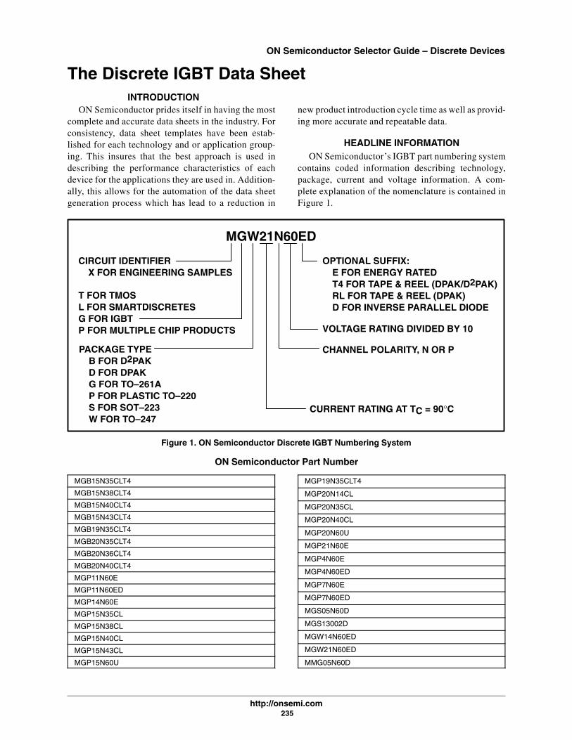
ON Semiconductor Selector Guide – Discrete Devices
http://onsemi.com 235
The Discrete IGBT Data SheetINTRODUCTION
ON Semiconductor prides itself in having the mostcomplete and accurate data sheets in the industry. Forconsistency, data sheet templates have been estab-lished for each technology and or application group-ing. This insures that the best approach is used indescribing the performance characteristics of eachdevice for the applications they are used in. Addition-ally, this allows for the automation of the data sheetgeneration process which has lead to a reduction in
new product introduction cycle time as well as provid-ing more accurate and repeatable data.
HEADLINE INFORMATIONON Semiconductor’s IGBT part numbering system
contains coded information describing technology,package, current and voltage information. A com-plete explanation of the nomenclature is contained inFigure 1.
MGW21N60ED
CIRCUIT IDENTIFIER X FOR ENGINEERING SAMPLES
T FOR TMOSL FOR SMARTDISCRETESG FOR IGBTP FOR MULTIPLE CHIP PRODUCTS
PACKAGE TYPEB FOR D2PAKD FOR DPAKG FOR TO–261AP FOR PLASTIC TO–220S FOR SOT–223W FOR TO–247
OPTIONAL SUFFIX:E FOR ENERGY RATEDT4 FOR TAPE & REEL (DPAK/D2PAK)RL FOR TAPE & REEL (DPAK)D FOR INVERSE PARALLEL DIODE
VOLTAGE RATING DIVIDED BY 10
CHANNEL POLARITY, N OR P
CURRENT RATING AT TC = 90°C
Figure 1. ON Semiconductor Discrete IGBT Numbering System
ON Semiconductor Part Number
MGB15N35CLT4
MGB15N38CLT4
MGB15N40CLT4
MGB15N43CLT4
MGB19N35CLT4
MGB20N35CLT4
MGB20N36CLT4
MGB20N40CLT4
MGP11N60E
MGP11N60ED
MGP14N60E
MGP15N35CL
MGP15N38CL
MGP15N40CL
MGP15N43CL
MGP15N60U
MGP19N35CLT4
MGP20N14CL
MGP20N35CL
MGP20N40CL
MGP20N60U
MGP21N60E
MGP4N60E
MGP4N60ED
MGP7N60E
MGP7N60ED
MGS05N60D
MGS13002D
MGW14N60ED
MGW21N60ED
MMG05N60D
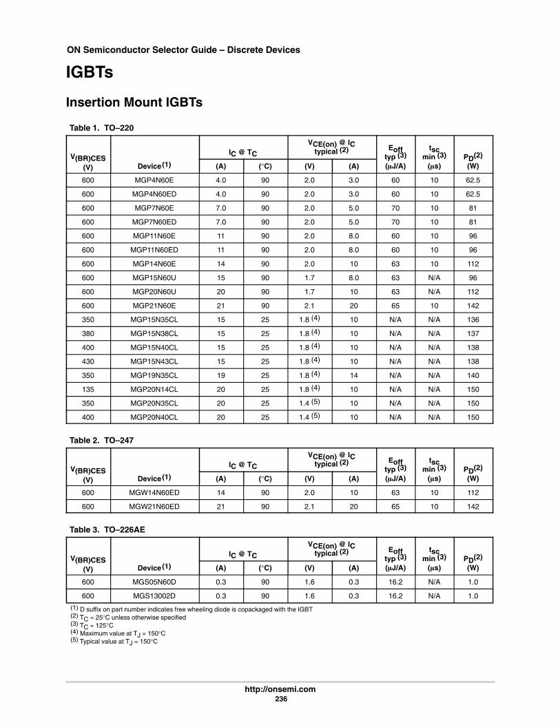
ON Semiconductor Selector Guide – Discrete Devices
http://onsemi.com 236
IGBTs
Insertion Mount IGBTs
Table 1. TO–220
V(BR)CES(1)
IC @ TC
VCE(on) @ ICtypical (2) Eoff
typ (3)tsc
min (3) PD(2)V(BR)CES(V) Device(1) (A) (°C) (V) (A)
typ ( )
(J/A)min ( )
(s)PD( )
(W)
600 MGP4N60E 4.0 90 2.0 3.0 60 10 62.5
600 MGP4N60ED 4.0 90 2.0 3.0 60 10 62.5
600 MGP7N60E 7.0 90 2.0 5.0 70 10 81
600 MGP7N60ED 7.0 90 2.0 5.0 70 10 81
600 MGP11N60E 11 90 2.0 8.0 60 10 96
600 MGP11N60ED 11 90 2.0 8.0 60 10 96
600 MGP14N60E 14 90 2.0 10 63 10 112
600 MGP15N60U 15 90 1.7 8.0 63 N/A 96
600 MGP20N60U 20 90 1.7 10 63 N/A 112
600 MGP21N60E 21 90 2.1 20 65 10 142
350 MGP15N35CL 15 25 1.8 (4) 10 N/A N/A 136
380 MGP15N38CL 15 25 1.8 (4) 10 N/A N/A 137
400 MGP15N40CL 15 25 1.8 (4) 10 N/A N/A 138
430 MGP15N43CL 15 25 1.8 (4) 10 N/A N/A 138
350 MGP19N35CL 19 25 1.8 (4) 14 N/A N/A 140
135 MGP20N14CL 20 25 1.8 (4) 10 N/A N/A 150
350 MGP20N35CL 20 25 1.4 (5) 10 N/A N/A 150
400 MGP20N40CL 20 25 1.4 (5) 10 N/A N/A 150
Table 2. TO–247
V(BR)CES(1)
IC @ TC
VCE(on) @ ICtypical (2) Eoff
typ (3)tsc
min (3) PD(2)V(BR)CES(V) Device(1) (A) (°C) (V) (A)
typ ( )
(J/A)min ( )
(s)PD( )
(W)
600 MGW14N60ED 14 90 2.0 10 63 10 112
600 MGW21N60ED 21 90 2.1 20 65 10 142
Table 3. TO–226AE
V(BR)CES(1)
IC @ TC
VCE(on) @ ICtypical (2) Eoff
typ (3)tsc
min (3) PD(2)V(BR)CES(V) Device(1) (A) (°C) (V) (A)
typ ( )
(J/A)min ( )
(s)PD( )
(W)
600 MGS05N60D 0.3 90 1.6 0.3 16.2 N/A 1.0
600 MGS13002D 0.3 90 1.6 0.3 16.2 N/A 1.0
1(1) D suffix on part number indicates free wheeling diode is copackaged with the IGBT1(2) TC = 25°C unless otherwise specified1(3) TC = 125°C1(4) Maximum value at TJ = 150°C1(5) Typical value at TJ = 150°C
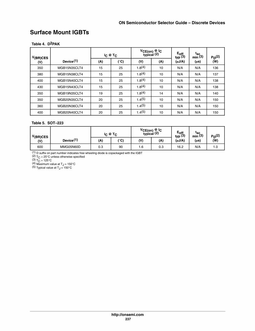
ON Semiconductor Selector Guide – Discrete Devices
http://onsemi.com 237
Surface Mount IGBTs
Table 4. D2PAK
V(BR)CES(1)
IC @ TC
VCE(on) @ ICtypical (2) Eoff
typ (3)tsc
min (3) PD(2)V(BR)CES(V) Device(1) (A) (°C) (V) (A)
typ ( )
(J/A)min ( )
(s)PD( )
(W)
350 MGB15N35CLT4 15 25 1.8(4) 10 N/A N/A 136
380 MGB15N38CLT4 15 25 1.8(4) 10 N/A N/A 137
400 MGB15N40CLT4 15 25 1.8(4) 10 N/A N/A 138
430 MGB15N43CLT4 15 25 1.8(4) 10 N/A N/A 138
350 MGB19N35CLT4 19 25 1.8(4) 14 N/A N/A 140
350 MGB20N35CLT4 20 25 1.4(5) 10 N/A N/A 150
360 MGB20N36CLT4 20 25 1.4(5) 10 N/A N/A 150
400 MGB20N40CLT4 20 25 1.4(5) 10 N/A N/A 150
Table 5. SOT–223
V(BR)CES(1)
IC @ TC
VCE(on) @ ICtypical (2) Eoff
typ (3)tsc
min (3) PD(2)V(BR)CES(V) Device(1) (A) (°C) (V) (A)
typ ( )
(J/A)min ( )
(s)PD( )
(W)
600 MMG05N60D 0.3 90 1.6 0.3 16.2 N/A 1.0
1(1) D suffix on part number indicates free wheeling diode is copackaged with the IGBT1(2) TC = 25°C unless otherwise specified1(3) TC = 125°C1(4) Maximum value at TJ = 150°C1(5) Typical value at TJ = 150°C

ON Semiconductor Selector Guide – Discrete Devices
http://onsemi.com 238
Symbols, Terms and Definitions
The following are the most commonly used letter symbols, terms and definitions associated with IGBTs:
Symbol Term Definition
V(BR)CER collector–emitter breakdown volt-age with (resistance between gateand emitter)
The breakdown voltage between the collector terminal andthe emitter terminal when the gate terminal is (as indicatedby the last subscript letter) as follows:
R = returned to the emitter terminal through a specifiedresistance.
V(BR)CES gate short–circuited to emitter S = short–circuited to the emitter terminal.
V(BR)CEV voltage between gate and emitter V = returned to the emitter terminal through a specifiedvoltage.
V(BR)CEX circuit between gate and emitter X = returned to the emitter terminal through a specifiedcircuit.
Cce collector–emitter capacitance The capacitance between the collector and emitter termi-nals with the gate terminal connected to the guard terminalof a three–terminal bridge.
Ccg collector–gate capacitance The same as Cres — See Cres.
Cge gate–emitter capacitance The capacitance between the gate and emitter terminalswith the collector terminal connected to the guard terminalof a three–terminal bridge.
Cies short–circuit input capacitance,common–emitter
The capacitance between the input terminals (gate andemitter) with the collector short–circuited to the emitter foralternating current. (Ref. IEEE No. 255)
Coes short–circuit output capacitance,common–emitter
The capacitance between the output terminals (collectorand emitter) with the gate short–circuited to the emitter foralternating current. (Ref. IEEE No. 255)
Cres short–circuit reverse transfercapacitance, common–emitter
The capacitance between the collector and gate terminalswith the emitter connected to the guard terminal of athree–terminal bridge.
Eoff turn–off energy loss Energy loss during turn–off measured over a period of timethat starts with 5% of test voltage and goes on for 5 s.
Eon turn–on energy loss Energy loss during turn–on measured from 5% of testcurrent to 5% of test voltage.
Ets total switching loss The sum of turn–on and turn–off energy losses.
gFE common–emitter large–signaltransconductance
The ratio of the change in collector current due to a changein gate–to–emitter voltage.
IC collector current, dc The direct current into the collector terminal.
IC(on) on–state collector current The direct current into the collector terminal with aspecified forward gate–emitter voltage applied to bias thedevice to the on–state.
ICES zero–gate–voltage collector current The direct current into the collector terminal when thegate–emitter voltage is zero.
IG gate current, dc The direct current into the gate terminal.
ON Semiconductor Selector Guide – Discrete Devices
http://onsemi.com 239
Symbol DefinitionTerm
IGESF forward gate current, collectorshort–circuited to emitter
The direct current into the gate terminal of an insulated–gate bipolar transistor with a forward gate–emitter voltageapplied and the collector terminal short–circuited to theemitter terminal.
IGESR reverse gate current, collectorshort–circuited to emitter
The direct current into the gate terminal of an insulated–gate bipolar transistor with a reverse gate–emitter voltageapplied and the collector terminal short–circuited to theemitter terminal.
IE emitter current, dc The direct current into the emitter terminal.
PT, PD total nonreactive power input to allterminals
The sum of the products of the dc input currents andvoltages.
Qg total gate charge The total gate charge required to charge the IGBTs inputcapacitance to VGE(on).
Qgc gate–to–collector charge The amount of charge required to charge the gate–to–collector capacitance to a specified value.
Qge gate–to–emitter charge The amount of charge required to charge the gate–to–emitter capacitance to a specified value.
RCE(on) static collector–emitter on–stateresistance
The dc resistance between the collector and emitterterminals with a specified gate–emitter voltage applied tobias the device to the on state.
RθCA thermal resistance, case–to–ambient
The thermal resistance (steady–state) from the devicecase to the ambient.
RθJA thermal resistance, junction–to–ambient
The thermal resistance (steady–state) from the semicon-ductor junction(s) to the ambient.
RθJC thermal resistance, junction–to–case
The thermal resistance (steady–state) from the semicon-ductor junction(s) to a stated location on the case.
RθJM thermal resistance, junction–to–mounting surface
The thermal resistance (steady–state) from the semicon-ductor junction(s) to a stated location on the mountingsurface.
TA ambient temperature or free–airtemperature
The air temperature measured below a device, in anenvironment of substantially uniform temperature, cooledonly by natural air convection and not materially affectedby reflective and radiant surfaces.
TC case temperature The temperature measured at a specified location on thecase of a device.
tc turn–off crossover time The time interval during which drain voltage rises from 10%of its peak off–state value and drain current falls to 10% ofits peak on–state value, in both cases ignoring spikes thatare not charge–carrier induced.
TJ channel temperature The temperature of the channel of an IGBT.
Tstg storage temperature The temperature at which the device, without any powerapplied, may be stored.
td(off) turn–off delay time Synonym for current turn–off delay time (see Note 1)*.
ON Semiconductor Selector Guide – Discrete Devices
http://onsemi.com 240
Symbol DefinitionTerm
td(off)i current turn–off delay time The interval during which an input pulse that is switchingthe transistor from a conducting to a nonconducting statefalls from 90% of its peak amplitude and the collectorcurrent waveform falls to 90% of its on–state amplitude,ignoring spikes that are not charge–carrier induced.
td(off)v voltage turn–off delay time The time interval during which an input pulse that isswitching the transistor from a conducting to a nonconduct-ing state falls from 90% of its peak amplitude and thecollector voltage waveform rises to 10% of its off–stateamplitude, ignoring spikes that are not charge–carrierinduced.
td(on) turn–on delay time Synonym for current turn–on delay time (see Note 1)*.
td(on)i current turn–on delay time The time interval during which can input pulse that isswitching the transistor from a nonconducting to a conduct-ing state rises from 10% of its peak amplitude and thecollector current waveform rises to 10% of its on–stateamplitude, ignoring spikes that are not charge–carrierinduced.
td(on)v voltage turn–on delay time The time interval during which an input pulse that isswitching the transistor from a nonconducting to a conduct-ing state rises from 10% of its peak amplitude and thecollector voltage waveform falls to 90% of its off–stateamplitude, ignoring spikes that are not charge–carrierinduced.
tf fall time Synonym for current fall time (see Note 1)*.
tfi current fall time The time interval during which the drain current changesfrom 90% to 10% of its peak off–state value, ignoringspikes that are not charge–carrier induced.
tfv voltage fall time The time interval during which the drain voltage changesfrom 90% to 10% of its peak off–state value, ignoringspikes that are not charge–carrier induced.
toff turn–off time Synonym for current turn–off time (see Note 1)*.
toff(i) current turn–off time The sum of current turn–off delay time and current fall time,i.e., td(off)i + tfi.
toff(v) voltage turn–off time The sum of voltage turn–off delay time and voltage risetime, i.e., td(off)v + trv.
ton turn–on time Synonym for current turn–on time (see Note 1)*.
ton(i) current turn–on time The sum of current turn–on delay time and current risetime, i.e., td(on)i + tri.
ton(v) voltage turn–on time The sum of voltage turn–on delay time and voltage falltime, i.e., td(on)v + tfv.
ON Semiconductor Selector Guide – Discrete Devices
http://onsemi.com 241
Symbol DefinitionTerm
tp pulse duration The time interval between a reference point on the leadingedge of a pulse waveform and a reference point on thetrailing edge of the same waveform.
Note: The two reference points are usually 90% of thesteady–state amplitude of the waveform existing after the leadingedge, measured with respect to the steady–state amplitudeexisting before the leading edge. If the reference points are 50%points, the symbol tw and term average pulse duration should beused.
tr rise time Synonym for current rise time (see Note 1)*.
tri current rise time The time interval during which the drain current changesfrom 10% to 90% of its peak on–state value, ignoringspikes that are not charge–carrier induced.
trv voltage rise time The time interval during which the collector voltagechanges from 10% to 90% of its peak off–state value,ignoring spikes that are not charge–carrier induced.
tsc short circuit withstand time The duration a device can withstand a short circuit at aspecified temperature and gate bias.
tw average pulse duration The time interval between a reference point on the leadingedge of a pulse waveform and a reference point on thetrailing edge of the same waveform, with both referencepoints being 50% of the steady–state amplitude of thewaveform existing after the leading edge, measured withrespect to the steady–state amplitude existing before theleading edge.
Note: If the reference points are not 50% points, the symbol tp andterm pulse duration should be used.
V(BR)GESF forward gate–emitter breakdownvoltage
The breakdown voltage between the gate and emitterterminals with a forward gate–emitter voltage applied andthe collector terminal short–circuited to the emitterterminal.
V(BR)GESR reverse gate–emitter breakdownvoltage
The breakdown voltage between the gate and emitterterminals with a reverse gate–emitter voltage applied andthe collector terminal short–circuited to the emitterterminal.
VCC, VGGVEE
supply voltage, dc (collector, gate,emitter) voltage
The dc supply voltage applied to a circuit or connected tothe reference terminal.
VCGVCEVGCVGEVECVEG
collector–to–gatecollector–to–emittergate–to–collectorgate–to–emitteremitter–to–collectoremitter–to–gate
The dc voltage between the terminal indicated by the firstsubscript and the reference terminal indicated by thesecond subscript (stated in terms of the polarity at theterminal indicated by the first subscript).
VCE(on) collector–emitter on–state voltage The voltage between the collector and emitter terminalswith a specified forward gate–emitter voltage applied tobias the device to the on state.
VCE(sat) collector–to–emitter saturationvoltage
Voltage measured from collector–to–emitter at a specifiedcollectorcurrent and gate–to–emitter voltage. Inter-changeable with VCE(on) for IGBTs.
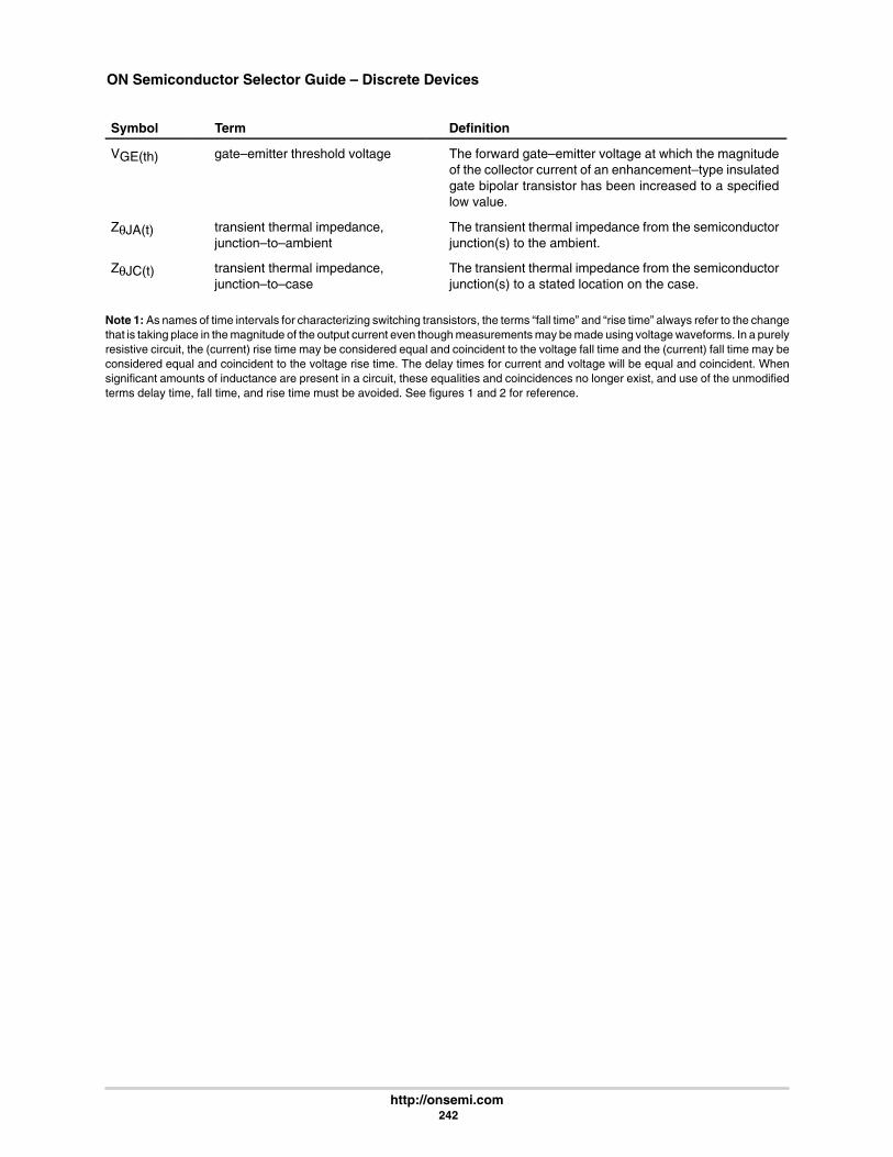
ON Semiconductor Selector Guide – Discrete Devices
http://onsemi.com 242
Symbol DefinitionTerm
VGE(th) gate–emitter threshold voltage The forward gate–emitter voltage at which the magnitudeof the collector current of an enhancement–type insulatedgate bipolar transistor has been increased to a specifiedlow value.
ZθJA(t) transient thermal impedance,junction–to–ambient
The transient thermal impedance from the semiconductorjunction(s) to the ambient.
ZθJC(t) transient thermal impedance,junction–to–case
The transient thermal impedance from the semiconductorjunction(s) to a stated location on the case.
Note 1: As names of time intervals for characterizing switching transistors, the terms “fall time” and “rise time” always refer to the changethat is taking place in the magnitude of the output current even though measurements may be made using voltage waveforms. In a purelyresistive circuit, the (current) rise time may be considered equal and coincident to the voltage fall time and the (current) fall time may beconsidered equal and coincident to the voltage rise time. The delay times for current and voltage will be equal and coincident. Whensignificant amounts of inductance are present in a circuit, these equalities and coincidences no longer exist, and use of the unmodifiedterms delay time, fall time, and rise time must be avoided. See figures 1 and 2 for reference.
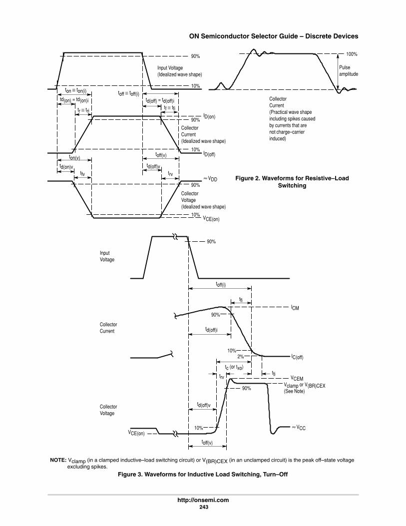
ON Semiconductor Selector Guide – Discrete Devices
http://onsemi.com 243
Figure 2. Waveforms for Resistive–LoadSwitching
Figure 3. Waveforms for Inductive Load Switching, Turn–Off
NOTE: Vclamp (in a clamped inductive–load switching circuit) or V(BR)CEX (in an unclamped circuit) is the peak off–state voltage excluding spikes.
90%
Input Voltage(Idealized wave shape)
10%
90%
10%
90%
10%
CollectorVoltage(Idealized wave shape)
CollectorCurrent(Idealized wave shape)
CollectorCurrent(Practical wave shapeincluding spikes causedby currents that arenot charge–carrierinduced)
toff ≅ toff(i)ton ≅ ton(i)
td(off) = td(off)i
ID(on)
tf ≅ tfi
td(off)v
ID(off)toff(v)
trvtfv
tr ≅ tri
td(on) = td(on)i
ton(v)
td(on)v
VCE(on)
100%
Pulseamplitude
VDD
90%
InputVoltage
2%10%
CollectorVoltage
CollectorCurrent
toff(i)
td(off)i
ICM
tfi
td(off)v
IC(off)
toff(v)
ttitrv VCEM
VCC
90%
10%
90%
tc (or txo)
Vclamp or V(BR)CEX(See Note)
VCE(on)

ON Semiconductor Selector Guide – Discrete Devices
http://onsemi.com 244
ABSOLUTE MAXIMUM RATINGS
Absolute maximum ratings represent the extremecapabilities of the device. They can best be described asdevice characterization boundaries and are given tofacilitate “worst–case” design.
Collector–to–Emitter Voltage (VCES, VCER) Thisrepresents the lower limit of the device’s blockingvoltage capability from Collector–to–Emitter when thegate is shorted to the source (VCES), or when a 1.0 MΩGate–to–Emitter resistor is present (VCER). It ismeasured at a specific leakage current and has a positivetemperature coefficient. The voltage across the IGBTshould never exceed this rating in order to preventbreakdown of the Collector–to–Emitter junction.
Maximum Gate–to–Emitter Voltage (VGE) The maxi-mum allowable Gate–to–Emitter voltage. Exceedingthis limit may result in permanent device degradation.
Continuous Collector Current (IC25, IC90) The dccurrent level that will raise the device’s junctiontemperature to its rated maximum while its casetemperature is held at either 25°C (IC25), or 90°C (IC90).This can be calculated by the equation:
ICXwhere,
= (TJMAX – TX) * (VCE(on) @ TJMAX) / RθJC
TXVCE(on)TJMAXRθJC
= Case temperature= Device’s “on” voltage= Device’s maximum rated junction temperature= Device’s thermal resistance junction–to–case
Pulsed Collector Current (ICM) The maximum allow-able peak collector current the device can safely handleunder a 10 s pulsed condition. This rating takes intoconsideration the device’s thermal limitation as well asVCE(on), wire bond and source metal limitations.
Maximum Power Dissipation (PD) Specifies the powerdissipation limit which takes the junction temperature toits maximum rating while the reference temperature isbeing held at 25° C. It is calculated by the followingequation:
PDwhere,
= (TJMAX – TR)/RθJR
PDTJMAXTRRθJR
= Maximum power dissipation= Maximum allowable junction temperature= Reference (case and or ambient) temperature= Thermal resistance junction–to–reference= (case or ambient)
Maximum Junction Temperature (TJMAX) This valuerepresents the maximum allowable junction tempera-ture of the device. It is derived and based off of long termreliability data. Exceeding this value will only serve toshorten the device’s long term operating life.
Short Circuit Withstand Time (tsc) The permissibletime, for given values of Collector–to–Emitter voltage,gate voltage and starting temperature, that the devicecan safely handle while in a shorted load condition.
Thermal Resistance (RθJC, RθJA) The quantity thatresists or impedes the flow of heat energy in a device iscalled thermal resistance. Thermal resistance values areneeded for proper thermal design. These values aremeasured as detailed in Section 3–8A.
ELECTRICAL CHARACTERISTICS
The intent of this section of the data sheet is to pro-vide detailed device characterization information sothat the designer can predict with a high degree of accu-racy the behavior of the device in a specific application.
Collector–to–Emitter Breakdown Voltage (V(BR)CES)This represents the lower limit of the device’s blockingvoltage capability from Collector–to–Emitter with thegate shorted to the source. It is measured at a specific leak-age current and has a positive temperature coefficient.
Zero Gate Voltage Collector Current (ICES) The directcurrent into the collector terminal of the device whenthe Gate–to–Emitter voltage is zero and the collectorterminal is reversed biased with respect to the sourceterminal. This parameter generally increases with tem-perature as shown in the “Collector–to–Emitter Leak-age Current versus Voltage” figure found in the device’sdata sheet.
Gate–Body Leakage Current (IGES) The direct currentflow in the gate terminal of the device when the gate ter-minal is biased with either a positive or negative voltagewith respect to the source terminal and the collector ter-minal is short–circuited to the source terminal.
Gate Threshold Voltage (VGE(th)) The forward Gate–to–Emitter voltage at which the magnitude of collectorcurrent has been increased to some low threshold value,usually specified as 250 a or 1.0 ma. This parameterhas a negative temperature coefficient.
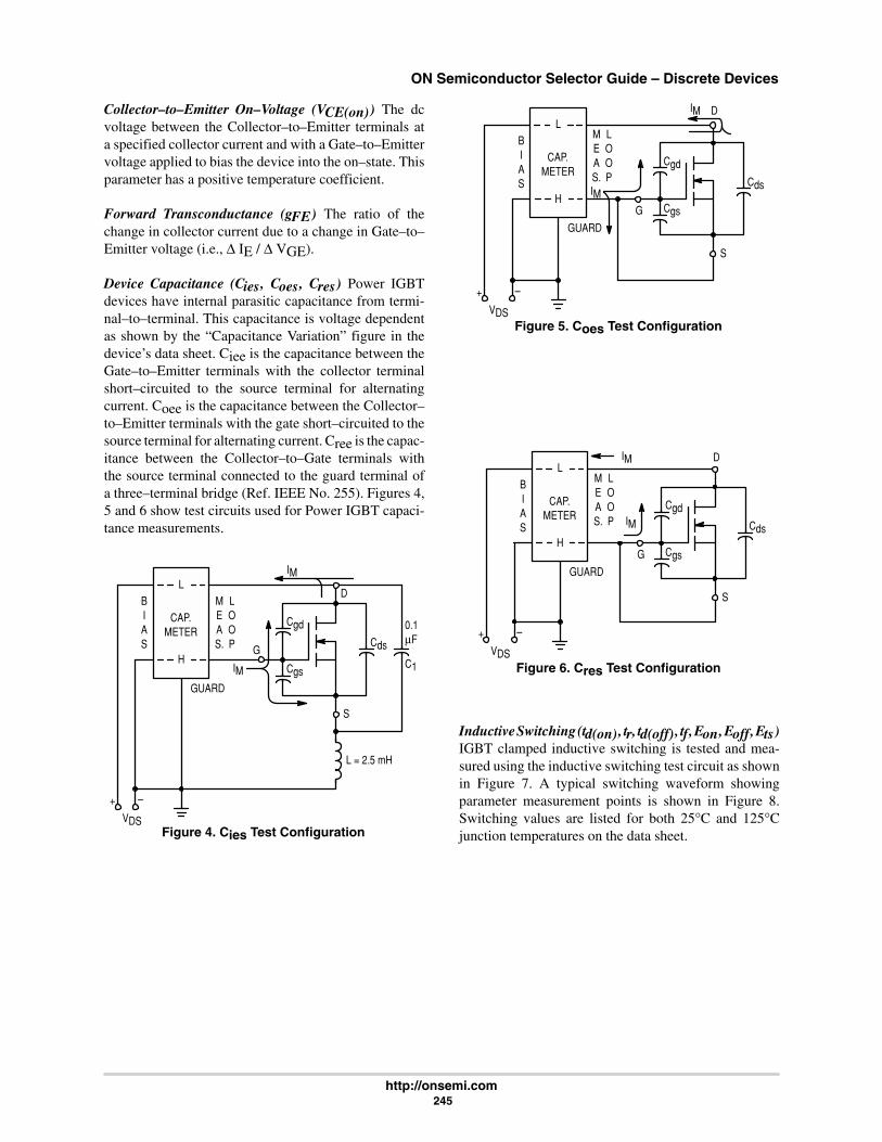
ON Semiconductor Selector Guide – Discrete Devices
http://onsemi.com 245
Collector–to–Emitter On–Voltage (VCE(on)) The dcvoltage between the Collector–to–Emitter terminals ata specified collector current and with a Gate–to–Emittervoltage applied to bias the device into the on–state. Thisparameter has a positive temperature coefficient.
Forward Transconductance (gFE) The ratio of thechange in collector current due to a change in Gate–to–Emitter voltage (i.e., ∆ IE / ∆ VGE).
Device Capacitance (Cies, Coes, Cres) Power IGBTdevices have internal parasitic capacitance from termi-nal–to–terminal. This capacitance is voltage dependentas shown by the “Capacitance Variation” figure in thedevice’s data sheet. Ciee is the capacitance between theGate–to–Emitter terminals with the collector terminalshort–circuited to the source terminal for alternatingcurrent. Coee is the capacitance between the Collector–to–Emitter terminals with the gate short–circuited to thesource terminal for alternating current. Cree is the capac-itance between the Collector–to–Gate terminals withthe source terminal connected to the guard terminal ofa three–terminal bridge (Ref. IEEE No. 255). Figures 4,5 and 6 show test circuits used for Power IGBT capaci-tance measurements.
L
H
CAP.METER
BIAS
MEAS.
LOOP
GUARD
+ –
VDS
L = 2.5 mH
Cds
C1
0.1µF
S
D
IM
Cgd
Cgs
G
IM
Figure 4. Cies Test Configuration
L
H
CAP.METER
BIAS
MEAS.
LOOP
GUARD
+ –
VDS
Cds
S
DIM
Cgd
CgsG
IM
Figure 5. Coes Test Configuration
L
H
CAP.METER
BIAS
MEAS.
LOOP
GUARD
+ –
VDS
Cds
S
DIM
Cgd
CgsG
IM
Figure 6. Cres Test Configuration
Inductive Switching (td(on), tr, td(off), tf, Eon, Eoff, Ets)IGBT clamped inductive switching is tested and mea-sured using the inductive switching test circuit as shownin Figure 7. A typical switching waveform showingparameter measurement points is shown in Figure 8.Switching values are listed for both 25°C and 125°Cjunction temperatures on the data sheet.

ON Semiconductor Selector Guide – Discrete Devices
http://onsemi.com 246
Figure 7. Switching Test Circuit
VGG
DC SUPPLY
DC RTN
IGBT
LOAD
RG
IL
LS
LE
OUTPUT, VoutINVERTED
INPUT, Vin10%
50%
90%
50%
90%90%
tr
10%
tftd(off)td(off)
ton toff
PULSE WIDTH
Figure 8. Switching Waveforms
Gate Charge (QT, Q1, Q2) Gate charge values are usedto size the gate drive circuit. QT is defined as the totalgate charge required to charge the device’s input capaci-tance to the applied gate voltage. Q1 is defined as thecharge required to charge the device’s input capacitanceCGE to the VGS(on) value required to maintain the testcurrent IC. Q2 is defined as the charge time required tocharge CGD to the same value as CGE.
Diode Forward Voltage Drop (VFEC) Co–PackageIGBT devices contain an integral power diode betweenthe Collector–to–Emitter terminals. The dc voltagebetween the Emitter–to–Collector terminals when thepower diode is forward biased is called the diode for-ward voltage drop (VFEC).
Reverse Recovery Time (trr, ta, tb, QRR) Co–PackageIGBT devices contain an integral power diode. A powerdiode is a minority carrier device and thus has a finitereverse recovery time. ta is defined as the time betweenthe dropping IS current’s zero crossing point to the peakIRM. tb is defined as the time between the peak IRM toa projected IRM zero current crossing point through a25% IRM projection as shown in Figure 9. Total reverserecovery time, trr, is defined as the sum of ta and tb. QRRis defined as the integral of the area made up by the IRMwaveform and VR, the reapplied blocking voltage whichforces reverse recovery. A relative softness factor s, isdefined as the ratio of tb to ta. General purpose rectifiershave a softness factor of around 1.0, fast recovery recti-fiers have a softness factor of approximately 0.5 and ul-tra fast rectifiers are very abrupt and have a softness fac-tor of around 0.2. The tradeoff is the rectifier speedversus softness. The higher the softness factor, the lessundesirable induced voltages in switching circuits.Diode reverse recovery values are listed for both 25°Cand 125°C junction temperatures on the data sheet.
Figure 9. Diode Reverse Recovery Waveform
di/dt
trrta
tp
IS
0.25 IS
TIME
IS
tb

Alphabetical Parts Listing
Device Number Page Device Number Page Device Number Page
http://onsemi.com 247
1.5KE100A 1711.5KE10A 1711.5KE110A 1711.5KE11A 1711.5KE120A 1711.5KE12A 1711.5KE130A 1711.5KE13A 1711.5KE150A 1721.5KE15A 1711.5KE160A 1721.5KE16A 1711.5KE170A 1721.5KE180A 1721.5KE18A 1711.5KE200A 1721.5KE20A 1711.5KE220A 1721.5KE22A 1711.5KE24A 1711.5KE250A 1721.5KE27A 1711.5KE30A 1711.5KE33A 1711.5KE36A 1711.5KE39A 1711.5KE43A 1711.5KE47A 1711.5KE51A 1711.5KE56A 1711.5KE6.8A 1711.5KE62A 1711.5KE68A 1711.5KE7.5A 1711.5KE75A 1711.5KE8.2A 1711.5KE82A 1711.5KE9.1A 1711.5KE91A 1711.5SMC10AT3 1801.5SMC11AT3 1801.5SMC12AT3 1801.5SMC13AT3 1801.5SMC15AT3 1801.5SMC16AT3 1801.5SMC18AT3 1801.5SMC20AT3 1801.5SMC22AT3 1801.5SMC24AT3 1801.5SMC27AT3 180
1.5SMC30AT3 1801.5SMC33AT3 1801.5SMC36AT3 1801.5SMC39AT3 1801.5SMC43AT3 1801.5SMC47AT3 1801.5SMC51AT3 1801.5SMC56AT3 1801.5SMC6.8AT3 1801.5SMC62AT3 1801.5SMC68AT3 1801.5SMC7.5AT3 1801.5SMC75AT3 1801.5SMC8.2AT3 1801.5SMC82AT3 1801.5SMC9.1AT3 1801.5SMC91AT3 1801M110ZS5 1631M120ZS5 1631M130ZS5 1631M150ZS5 1631M160ZS5 1631M180ZS5 1631M200ZS5 1631N4004 2141N4007 2141N4678 1621N4679 1621N4680 1621N4681 1621N4682 1621N4683 1621N4684 1621N4685 1621N4686 1621N4687 1621N4688 1621N4689 1621N4690 1621N4691 1621N4692 1621N4693 1621N4694 1621N4695 1621N4696 1621N4697 1621N4698 1621N4699 1621N4700 1621N4701 162
1N4702 1621N4703 1621N4704 1621N4705 1621N4706 1621N4707 1621N4708 1621N4709 1621N4710 1631N4711 1631N4712 1631N4713 1631N4714 1631N4715 1631N4716 1631N4717 1631N4728A 1621N4729A 1621N4730A 1621N4731A 1621N4732A 1621N4733A 1621N4734A 1621N4735A 1621N4736A 1621N4737A 1621N4738A 1621N4739A 1621N4740A 1621N4741A 1621N4742A 1621N4743A 1621N4744A 1621N4745A 1621N4746A 1621N4747A 1621N4748A 1621N4749A 1621N4750A 1631N4751A 1631N4752A 1631N4753A 1631N4754A 1631N4755A 1631N4756A 1631N4757A 1631N4758A 1631N4759A 1631N4760A 1631N4761A 163
Alphabetical Parts Listing
Device Number Page Device Number Page Device Number Page
http://onsemi.com 248
1N4762A 1631N4763A 1631N4764A 1631N4935 2141N4937 2141N5222B 1621N5223B 1621N5224B 1621N5225B 1621N5226B 1621N5227B 1621N5228B 1621N5229B 1621N5230B 1621N5231B 1621N5232B 1621N5233B 1621N5234B 1621N5235B 1621N5236B 1621N5237B 1621N5238B 1621N5239B 1621N5240B 1621N5241B 1621N5242B 1621N5243B 1621N5244B 1621N5245B 1621N5246B 1621N5247B 1621N5248B 1621N5249B 1621N5250B 1621N5251B 1621N5252B 1621N5253B 1631N5254B 1631N5255B 1631N5256B 1631N5257B 1631N5258B 1631N5259B 1631N5260B 1631N5261B 1631N5262B 1631N5263B 1631N5264B 1631N5265B 1631N5266B 163
1N5267B 1631N5268B 1631N5269B 1631N5270B 1631N5333B 1621N5334B 1621N5335B 1621N5336B 1621N5337B 1621N5338B 1621N5339B 1621N5340B 1621N5341B 1621N5342B 1621N5343B 1621N5344B 1621N5345B 1621N5346B 1621N5347B 1621N5348B 1621N5349B 1621N5350B 1621N5351B 1621N5352B 1621N5353B 1621N5354B 1621N5355B 1621N5356B 1621N5357B 1621N5358B 1621N5359B 1621N5360B 1631N5361B 1631N5362B 1631N5363B 1631N5364B 1631N5365B 1631N5366B 1631N5367B 1631N5368B 1631N5369B 1631N5370B 1631N5371B 1631N5372B 1631N5373B 1631N5374B 1631N5375B 1631N5376B 1631N5377B 1631N5378B 163
1N5379B 1631N5380B 1631N5381B 1631N5382B 1631N5383B 1631N5384B 1631N5385B 1631N5386B 1631N5387B 1631N5388B 1631N5404 2141N5406 2141N5521B 1621N5817 2091N5818 2091N5819 2091N5820 2091N5821 2091N5822 2091N5908 1701N5913B 1621N5914B 1621N5915B 1621N5916B 1621N5917B 1621N5918B 1621N5919B 1621N5920B 1621N5921B 1621N5922B 1621N5923B 1621N5924B 1621N5925B 1621N5926B 1621N5927B 1621N5928B 1621N5929B 1621N5930B 1621N5931B 1621N5932B 1621N5933B 1621N5934B 1621N5935B 1631N5936B 1631N5937B 1631N5938B 1631N5939B 1631N5940B 1631N5941B 1631N5942B 163

Alphabetical Parts Listing
Device Number Page Device Number Page Device Number Page
http://onsemi.com 249
1N5943B 1631N5944B 1631N5945B 1631N5946B 1631N5947B 1631N5948B 1631N5949B 1631N5950B 1631N5951B 1631N5952B 1631N5953B 1631N5954B 1631N5955B 1631N5956B 1631N6267A 1711N6268A 1711N6269A 1711N6270A 1711N6271A 1711N6272A 1711N6273A 1711N6274A 1711N6275A 1711N6276A 1711N6277A 1711N6278A 1711N6279A 1711N6280A 1711N6281A 1711N6282A 1711N6283A 1711N6284A 1711N6285A 1711N6286A 1711N6287A 1711N6288A 1711N6289A 1711N6290A 1711N6291A 1711N6292A 1711N6293A 1711N6294A 1711N6295A 1711N6296A 1711N6297A 1711N6298A 1711N6299A 1721N6300A 1721N6301A 1721N6302A 172
1N6303A 1721N6373 1701N6374 1701N6375 1701N6376 1701N6377 1701N6378 1701N6379 1701N6380 1701N6381 1701N6382 1701N6383 1701N6384 1701N6385 1701N6386 1701N6387 1701N6388 1701N6389 1701SMA10AT3 1731SMA10CAT3 1741SMA11AT3 1731SMA11CAT3 1741SMA12AT3 1731SMA12CAT3 1741SMA13AT3 1731SMA13CAT3 1741SMA14AT3 1731SMA14CAT3 1741SMA15AT3 1731SMA15CAT3 1741SMA16AT3 1731SMA16CAT3 1741SMA17AT3 1731SMA17CAT3 1741SMA18AT3 1731SMA18CAT3 1741SMA20AT3 1731SMA20CAT3 1741SMA22AT3 1731SMA22CAT3 1741SMA24AT3 1731SMA26AT3 1731SMA26CAT3 1741SMA28AT3 1731SMA28CAT3 1741SMA30AT3 1731SMA30CAT3 1741SMA33AT3 1731SMA33CAT3 1741SMA36AT3 173
1SMA36CAT3 1741SMA40AT3 1731SMA40CAT3 1741SMA43AT3 1731SMA43CAT3 1741SMA45AT3 1731SMA45CAT3 1741SMA48AT3 1731SMA48CAT3 1741SMA5.0AT3 1731SMA51AT3 1731SMA51CAT3 1741SMA54AT3 1731SMA54CAT3 1741SMA58AT3 1731SMA58CAT3 1741SMA5913BT3 1641SMA5914BT3 1641SMA5915BT3 1641SMA5916BT3 1641SMA5917BT3 1641SMA5918BT3 1641SMA5919BT3 1641SMA5920BT3 1641SMA5921BT3 1641SMA5922BT3 1641SMA5923BT3 1641SMA5924BT3 1641SMA5925BT3 1641SMA5926BT3 1641SMA5927BT3 1641SMA5928BT3 1641SMA5929BT3 1641SMA5930BT3 1641SMA5931BT3 1641SMA5932BT3 1641SMA5933BT3 1641SMA5934BT3 1641SMA5935BT3 1641SMA5936BT3 1641SMA5937BT3 1641SMA5938BT3 1641SMA5939BT3 1641SMA5940BT3 1651SMA5941BT3 1651SMA5942BT3 1651SMA5943BT3 1651SMA5944BT3 1651SMA5945BT3 1651SMA6.0AT3 173

Alphabetical Parts Listing
Device Number Page Device Number Page Device Number Page
http://onsemi.com 250
1SMA6.5AT3 1731SMA60AT3 1731SMA60CAT3 1741SMA64AT3 1731SMA64CAT3 1741SMA7.0AT3 1731SMA7.5AT3 1731SMA70AT3 1731SMA70CAT3 1741SMA75AT3 1731SMA75CAT3 1741SMA78AT3 1731SMA78CAT3 1741SMA8.0AT3 1731SMA8.5AT3 1731SMA9.0AT3 1731SMB100AT3 1751SMB10AT3 1751SMB10CAT3 1761SMB110AT3 1751SMB11AT3 1751SMB11CAT3 1761SMB120AT3 1751SMB12AT3 1751SMB12CAT3 1761SMB130AT3 1751SMB13AT3 1751SMB13CAT3 1761SMB14AT3 1751SMB14CAT3 1761SMB150AT3 1751SMB15AT3 1751SMB15CAT3 1761SMB160AT3 1751SMB16AT3 1751SMB16CAT3 1761SMB170AT3 1751SMB17AT3 1751SMB17CAT3 1761SMB18AT3 1751SMB18CAT3 1761SMB20AT3 1751SMB20CAT3 1761SMB22AT3 1751SMB22CAT3 1761SMB24AT3 1751SMB24CAT3 1761SMB26AT3 1751SMB26CAT3 1761SMB28AT3 175
1SMB28CAT3 1761SMB30AT3 1751SMB30CAT3 1761SMB33AT3 1751SMB33CAT3 1761SMB36AT3 1751SMB36CAT3 1761SMB40AT3 1751SMB40CAT3 1761SMB43AT3 1751SMB43CAT3 1761SMB45AT3 1751SMB45CAT3 1761SMB48AT3 1751SMB48CAT3 1761SMB5.0AT3 1751SMB51AT3 1751SMB51CAT3 1761SMB54AT3 1751SMB54CAT3 1761SMB58AT3 1751SMB58CAT3 1761SMB5913BT3 1641SMB5914BT3 1641SMB5915BT3 1641SMB5916BT3 1641SMB5917BT3 1641SMB5918BT3 1641SMB5919BT3 1641SMB5920BT3 1641SMB5921BT3 1641SMB5922BT3 1641SMB5923BT3 1641SMB5924BT3 1641SMB5925BT3 1641SMB5926BT3 1641SMB5927BT3 1641SMB5928BT3 1641SMB5929BT3 1641SMB5930BT3 1641SMB5931BT3 1641SMB5932BT3 1641SMB5933BT3 1641SMB5934BT3 1641SMB5935BT3 1641SMB5936BT3 1641SMB5937BT3 1641SMB5938BT3 1641SMB5939BT3 1641SMB5940BT3 165
1SMB5941BT3 1651SMB5942BT3 1651SMB5943BT3 1651SMB5944BT3 1651SMB5945BT3 1651SMB5946BT3 1651SMB5947BT3 1651SMB5948BT3 1651SMB5949BT3 1651SMB5950BT3 1651SMB5951BT3 1651SMB5952BT3 1651SMB5953BT3 1651SMB5954BT3 1651SMB5955BT3 1651SMB5956BT3 1651SMB6.0AT3 1751SMB6.5AT3 1751SMB60AT3 1751SMB60CAT3 1761SMB64AT3 1751SMB64CAT3 1761SMB7.0AT3 1751SMB7.5AT3 1751SMB70AT3 1751SMB70CAT3 1761SMB75AT3 1751SMB75CAT3 1761SMB78AT3 1751SMB78CAT3 1761SMB8.0AT3 1751SMB8.5AT3 1751SMB85AT3 1751SMB9.0AT3 1751SMB90AT3 1751SMC10AT3 1791SMC11AT3 1791SMC12AT3 1791SMC13AT3 1791SMC14AT3 1791SMC15AT3 1791SMC16AT3 1791SMC17AT3 1791SMC18AT3 1791SMC20AT3 1791SMC22AT3 1791SMC24AT3 1791SMC26AT3 1791SMC28AT3 1791SMC30AT3 179
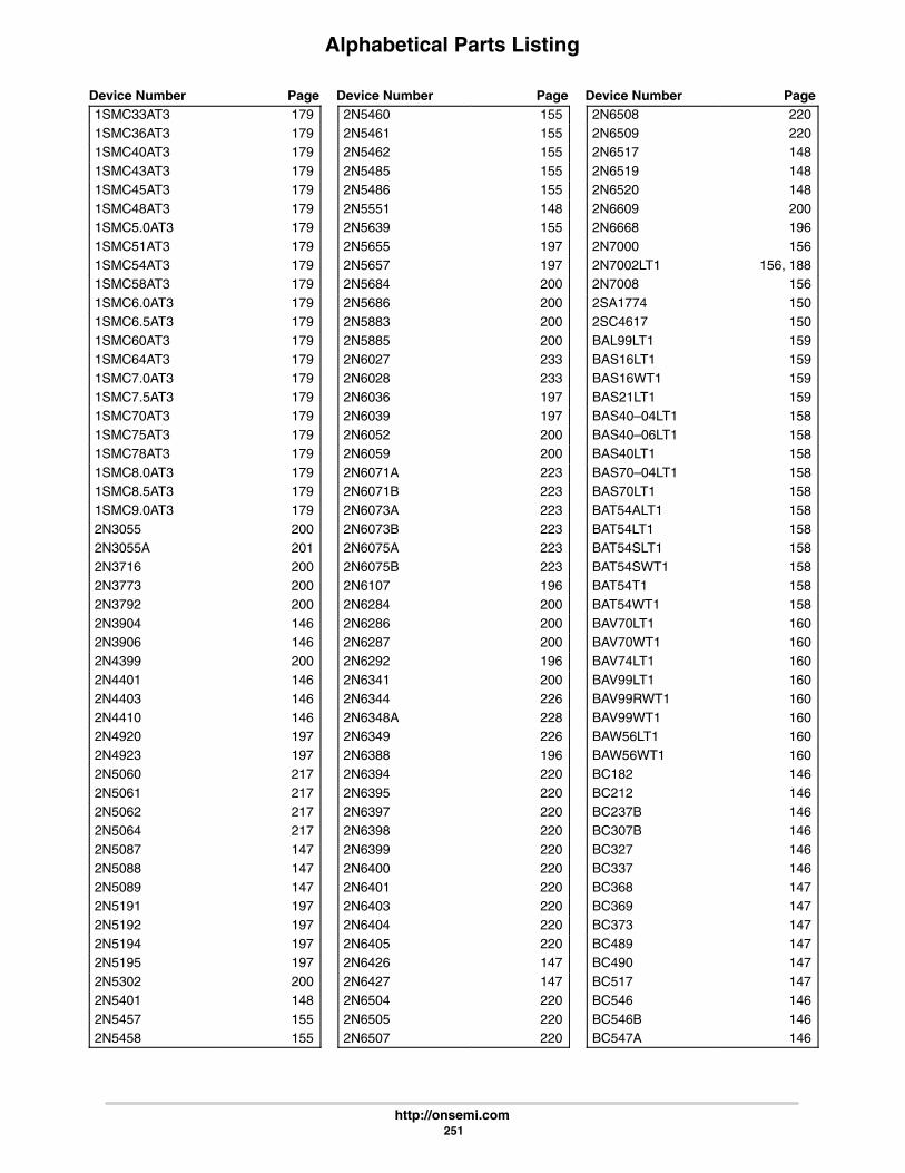
Alphabetical Parts Listing
Device Number Page Device Number Page Device Number Page
http://onsemi.com 251
1SMC33AT3 1791SMC36AT3 1791SMC40AT3 1791SMC43AT3 1791SMC45AT3 1791SMC48AT3 1791SMC5.0AT3 1791SMC51AT3 1791SMC54AT3 1791SMC58AT3 1791SMC6.0AT3 1791SMC6.5AT3 1791SMC60AT3 1791SMC64AT3 1791SMC7.0AT3 1791SMC7.5AT3 1791SMC70AT3 1791SMC75AT3 1791SMC78AT3 1791SMC8.0AT3 1791SMC8.5AT3 1791SMC9.0AT3 1792N3055 2002N3055A 2012N3716 2002N3773 2002N3792 2002N3904 1462N3906 1462N4399 2002N4401 1462N4403 1462N4410 1462N4920 1972N4923 1972N5060 2172N5061 2172N5062 2172N5064 2172N5087 1472N5088 1472N5089 1472N5191 1972N5192 1972N5194 1972N5195 1972N5302 2002N5401 1482N5457 1552N5458 155
2N5460 1552N5461 1552N5462 1552N5485 1552N5486 1552N5551 1482N5639 1552N5655 1972N5657 1972N5684 2002N5686 2002N5883 2002N5885 2002N6027 2332N6028 2332N6036 1972N6039 1972N6052 2002N6059 2002N6071A 2232N6071B 2232N6073A 2232N6073B 2232N6075A 2232N6075B 2232N6107 1962N6284 2002N6286 2002N6287 2002N6292 1962N6341 2002N6344 2262N6348A 2282N6349 2262N6388 1962N6394 2202N6395 2202N6397 2202N6398 2202N6399 2202N6400 2202N6401 2202N6403 2202N6404 2202N6405 2202N6426 1472N6427 1472N6504 2202N6505 2202N6507 220
2N6508 2202N6509 2202N6517 1482N6519 1482N6520 1482N6609 2002N6668 1962N7000 1562N7002LT1 156, 1882N7008 1562SA1774 1502SC4617 150BAL99LT1 159BAS16LT1 159BAS16WT1 159BAS21LT1 159BAS40–04LT1 158BAS40–06LT1 158BAS40LT1 158BAS70–04LT1 158BAS70LT1 158BAT54ALT1 158BAT54LT1 158BAT54SLT1 158BAT54SWT1 158BAT54T1 158BAT54WT1 158BAV70LT1 160BAV70WT1 160BAV74LT1 160BAV99LT1 160BAV99RWT1 160BAV99WT1 160BAW56LT1 160BAW56WT1 160BC182 146BC212 146BC237B 146BC307B 146BC327 146BC337 146BC368 147BC369 147BC373 147BC489 147BC490 147BC517 147BC546 146BC546B 146BC547A 146
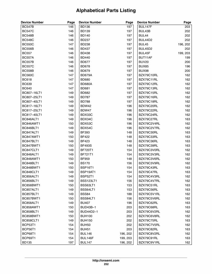
Alphabetical Parts Listing
Device Number Page Device Number Page Device Number Page
http://onsemi.com 252
BC547B 146BC547C 146BC548B 146BC548C 146BC550C 147BC556B 146BC557 146BC557A 146BC557B 146BC557C 146BC558B 146BC560C 147BC618 147BC639 147BC640 147BC807–16LT1 149BC807–25LT1 149BC807–40LT1 149BC817–16LT1 149BC817–25LT1 149BC817–40LT1 149BC846ALT1 149BC846AWT1 150BC846BLT1 149BC847ALT1 149BC847AWT1 150BC847BLT1 149BC847BWT1 150BC847CLT1 149BC848ALT1 149BC848AWT1 150BC848BLT1 149BC848BWT1 150BC848CLT1 149BC856ALT1 149BC856BLT1 149BC856BWT1 150BC857ALT1 149BC857BLT1 149BC857BWT1 150BC858ALT1 149BC858AWT1 150BC858BLT1 149BC858BWT1 150BC858CLT1 149BCP53T1 154BCP56T1 154BCP68T1 154BCP69T1 154BD135 197
BD136 197BD139 197BD140 197BD237 197BD238 197BD437 197BD438 197BD440 197BD677 197BD678 197BD679 197BD679A 197BD680 197BD680A 197BD681 197BD682 197BD787 197BD788 197BDW42 196BDW47 196BDX33C 196BDX34C 196BDX53C 196BDX54C 196BF393 148BF422 148BF423 148BF493S 148BF720T1 154BF721T1 154BF959 148BS170 156BSP16T1 154BSP19AT1 154BSP52T1 154BSS123LT1 156BSS63LT1 153BSS64LT1 153BSS84 188BSS84LT1 156BU407 196BUD43B–1 203BUD44D2–1 203BUH100 202BUH150 202BUH50 202BUH51 203BUL146 196, 202BUL146F 199, 203BUL147 196, 202
BUL147F 203BUL43B 202BUL44 202BUL44D2 202BUL45 196, 202BUL45D2 202BUL45F 199, 203BUT11AF 199BUV20 200BUX85 196BUX98 200BZX79C10RL 162BZX79C11RL 162BZX79C12RL 162BZX79C13RL 162BZX79C15RL 162BZX79C16RL 162BZX79C18RL 162BZX79C20RL 162BZX79C22RL 162BZX79C24RL 162BZX79C27RL 163BZX79C2V4RL 162BZX79C2V7RL 162BZX79C30RL 163BZX79C33RL 163BZX79C36RL 163BZX79C39RL 163BZX79C3V0RL 162BZX79C3V3RL 162BZX79C3V6RL 162BZX79C3V9RL 162BZX79C43RL 163BZX79C47RL 163BZX79C4V3RL 162BZX79C4V7RL 162BZX79C51RL 163BZX79C56RL 163BZX79C5V1RL 162BZX79C5V6RL 162BZX79C62RL 163BZX79C68RL 163BZX79C6V2RL 162BZX79C6V8RL 162BZX79C75RL 163BZX79C7V5RL 162BZX79C82RL 163BZX79C8V2RL 162BZX79C91RL 163BZX79C9V1RL 162
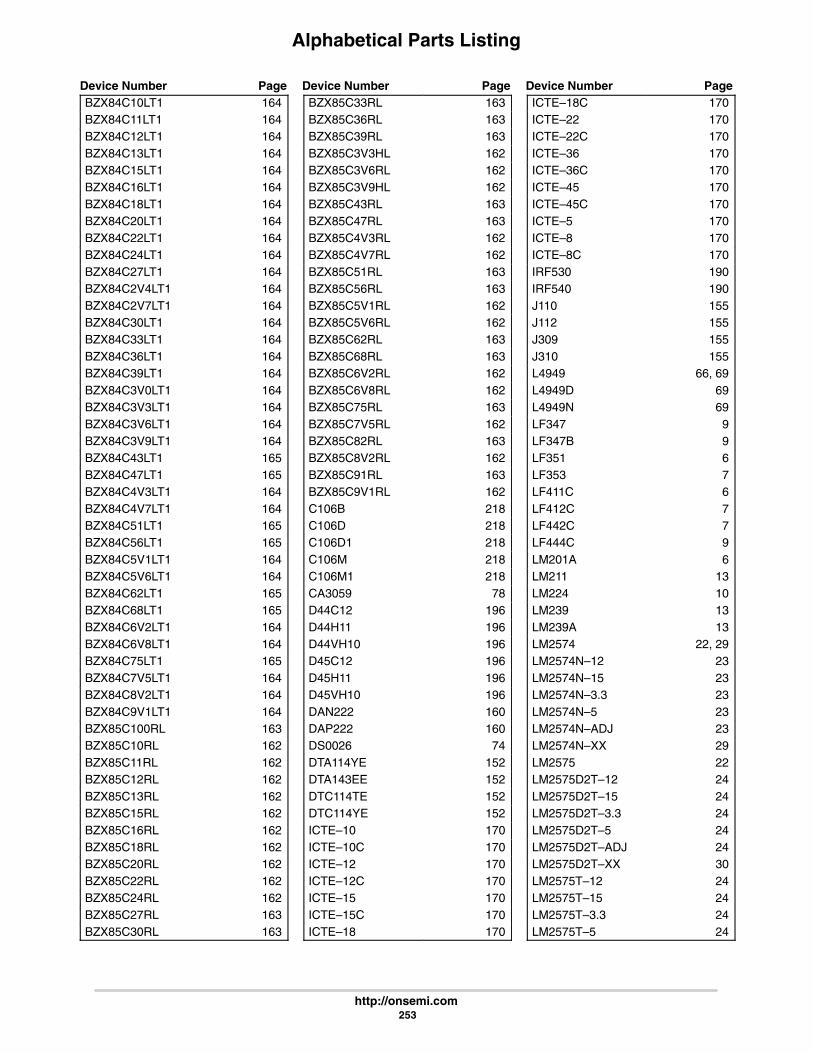
Alphabetical Parts Listing
Device Number Page Device Number Page Device Number Page
http://onsemi.com 253
BZX84C10LT1 164BZX84C11LT1 164BZX84C12LT1 164BZX84C13LT1 164BZX84C15LT1 164BZX84C16LT1 164BZX84C18LT1 164BZX84C20LT1 164BZX84C22LT1 164BZX84C24LT1 164BZX84C27LT1 164BZX84C2V4LT1 164BZX84C2V7LT1 164BZX84C30LT1 164BZX84C33LT1 164BZX84C36LT1 164BZX84C39LT1 164BZX84C3V0LT1 164BZX84C3V3LT1 164BZX84C3V6LT1 164BZX84C3V9LT1 164BZX84C43LT1 165BZX84C47LT1 165BZX84C4V3LT1 164BZX84C4V7LT1 164BZX84C51LT1 165BZX84C56LT1 165BZX84C5V1LT1 164BZX84C5V6LT1 164BZX84C62LT1 165BZX84C68LT1 165BZX84C6V2LT1 164BZX84C6V8LT1 164BZX84C75LT1 165BZX84C7V5LT1 164BZX84C8V2LT1 164BZX84C9V1LT1 164BZX85C100RL 163BZX85C10RL 162BZX85C11RL 162BZX85C12RL 162BZX85C13RL 162BZX85C15RL 162BZX85C16RL 162BZX85C18RL 162BZX85C20RL 162BZX85C22RL 162BZX85C24RL 162BZX85C27RL 163BZX85C30RL 163
BZX85C33RL 163BZX85C36RL 163BZX85C39RL 163BZX85C3V3HL 162BZX85C3V6RL 162BZX85C3V9HL 162BZX85C43RL 163BZX85C47RL 163BZX85C4V3RL 162BZX85C4V7RL 162BZX85C51RL 163BZX85C56RL 163BZX85C5V1RL 162BZX85C5V6RL 162BZX85C62RL 163BZX85C68RL 163BZX85C6V2RL 162BZX85C6V8RL 162BZX85C75RL 163BZX85C7V5RL 162BZX85C82RL 163BZX85C8V2RL 162BZX85C91RL 163BZX85C9V1RL 162C106B 218C106D 218C106D1 218C106M 218C106M1 218CA3059 78D44C12 196D44H11 196D44VH10 196D45C12 196D45H11 196D45VH10 196DAN222 160DAP222 160DS0026 74DTA114YE 152DTA143EE 152DTC114TE 152DTC114YE 152ICTE–10 170ICTE–10C 170ICTE–12 170ICTE–12C 170ICTE–15 170ICTE–15C 170ICTE–18 170
ICTE–18C 170ICTE–22 170ICTE–22C 170ICTE–36 170ICTE–36C 170ICTE–45 170ICTE–45C 170ICTE–5 170ICTE–8 170ICTE–8C 170IRF530 190IRF540 190J110 155J112 155J309 155J310 155L4949 66, 69L4949D 69L4949N 69LF347 9LF347B 9LF351 6LF353 7LF411C 6LF412C 7LF442C 7LF444C 9LM201A 6LM211 13LM224 10LM239 13LM239A 13LM2574 22, 29LM2574N–12 23LM2574N–15 23LM2574N–3.3 23LM2574N–5 23LM2574N–ADJ 23LM2574N–XX 29LM2575 22LM2575D2T–12 24LM2575D2T–15 24LM2575D2T–3.3 24LM2575D2T–5 24LM2575D2T–ADJ 24LM2575D2T–XX 30LM2575T–12 24LM2575T–15 24LM2575T–3.3 24LM2575T–5 24

Alphabetical Parts Listing
Device Number Page Device Number Page Device Number Page
http://onsemi.com 254
LM2575T–ADJ 24LM2575T–XX 30LM2575TV–12 24LM2575TV–15 24LM2575TV–3.3 24LM2575TV–5 24LM2575TV–ADJ 24LM2575TV–XX 30LM2576 22LM2576D2T–12 24LM2576D2T–15 24LM2576D2T–3.3 24LM2576D2T–5 24LM2576D2T–ADJ 24LM2576D2T–XX 30LM2576T–XX 30LM2576TV–12 24LM2576TV–15 24LM2576TV–3.3 24LM2576TV–5 24LM2576TV–ADJ 24LM2576TV–XX 30LM258 8LM285Z–1.2 53LM285Z–2.5 53LM2901 13LM2901V 13LM2902 10LM2902V 10LM2903 13LM2903V 13LM2904 8LM2904V 9LM2931 55, 57LM2931 Series 66LM2931A 57LM2931A–5.0 55LM2931C 58LM2935 57, 66LM301A 6LM308A 6LM311 13LM317 58LM317B 58LM317L 58LM317M 58LM323 56LM323A 56LM324 9LM324A 9
LM337 58LM337B 58LM337M 58LM339 13LM339A 13LM340 56LM340A–XX 56LM350 58LM350B 58LM358 7LM385BZ–1.2 53LM385BZ–2.5 53LM385Z–1.2 53LM385Z–2.5 53LM393 13LM393A 13LM833 7LP2950AC 55, 57LP2950C 55, 57LP2951AC 57, 58LP2951C 57, 58LT1585A 65LT1585ACM 65LT1585ACM–1.5 65LT1585ACT 65LT1585ACT–1.5 65M1MA141KT1 159M1MA141WAT1 160M1MA141WKT1 160M1MA142KT1 159M1MA142WAT1 160M1MA142WKT1 160M1MA151AT1 159M1MA151KT1 159M1MA151WAT1 160M1MA151WKT1 160M1MA174T1 159MAC08MT1 222MAC12D 228MAC12HCD 227MAC12HCM 227MAC12HCN 227MAC12M 228MAC12N 228MAC15A10 228MAC15A10FP 232MAC15A6 228MAC15A6FP 232MAC15A8 228MAC15A8FP 232
MAC15M 228MAC15N 228MAC15SM 228MAC15SN 228MAC16CD 229MAC16CM 229MAC16CN 229MAC16D 228MAC16HCD 229MAC16HCM 229MAC16HCN 229MAC16M 228MAC16N 228MAC210A10FP 231MAC210A8 227MAC210A8FP 231MAC212A10 227MAC212A10FP 231MAC212A6FP 231MAC212A8 227MAC212A8FP 231MAC218A10FP 231MAC218A6FP 231MAC218A8 225MAC223A10 230MAC223A10FP 232MAC223A6 230MAC223A6FP 232MAC223A8 230MAC223A8FP 232MAC224A10 230MAC224A4 230MAC224A6 230MAC224A8 230MAC228A10 226MAC228A4 226MAC228A6 226MAC228A8 226MAC229A8FP 231MAC320A8FP 232MAC4DCM 223MAC4DCN 223MAC4DHM 223MAC4DLM 223MAC4DSM 223MAC4DSN 223MAC4M 224MAC4N 224MAC4SM 224MAC4SN 224
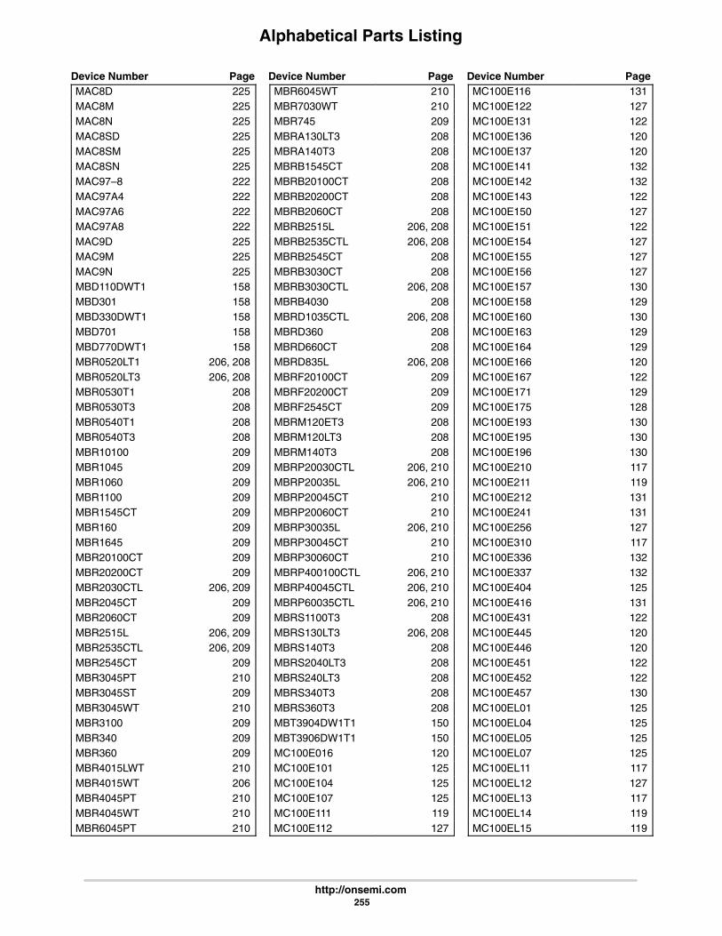
Alphabetical Parts Listing
Device Number Page Device Number Page Device Number Page
http://onsemi.com 255
MAC8D 225MAC8M 225MAC8N 225MAC8SD 225MAC8SM 225MAC8SN 225MAC97–8 222MAC97A4 222MAC97A6 222MAC97A8 222MAC9D 225MAC9M 225MAC9N 225MBD110DWT1 158MBD301 158MBD330DWT1 158MBD701 158MBD770DWT1 158MBR0520LT1 206, 208MBR0520LT3 206, 208MBR0530T1 208MBR0530T3 208MBR0540T1 208MBR0540T3 208MBR10100 209MBR1045 209MBR1060 209MBR1100 209MBR1545CT 209MBR160 209MBR1645 209MBR20100CT 209MBR20200CT 209MBR2030CTL 206, 209MBR2045CT 209MBR2060CT 209MBR2515L 206, 209MBR2535CTL 206, 209MBR2545CT 209MBR3045PT 210MBR3045ST 209MBR3045WT 210MBR3100 209MBR340 209MBR360 209MBR4015LWT 210MBR4015WT 206MBR4045PT 210MBR4045WT 210MBR6045PT 210
MBR6045WT 210MBR7030WT 210MBR745 209MBRA130LT3 208MBRA140T3 208MBRB1545CT 208MBRB20100CT 208MBRB20200CT 208MBRB2060CT 208MBRB2515L 206, 208MBRB2535CTL 206, 208MBRB2545CT 208MBRB3030CT 208MBRB3030CTL 206, 208MBRB4030 208MBRD1035CTL 206, 208MBRD360 208MBRD660CT 208MBRD835L 206, 208MBRF20100CT 209MBRF20200CT 209MBRF2545CT 209MBRM120ET3 208MBRM120LT3 208MBRM140T3 208MBRP20030CTL 206, 210MBRP20035L 206, 210MBRP20045CT 210MBRP20060CT 210MBRP30035L 206, 210MBRP30045CT 210MBRP30060CT 210MBRP400100CTL 206, 210MBRP40045CTL 206, 210MBRP60035CTL 206, 210MBRS1100T3 208MBRS130LT3 206, 208MBRS140T3 208MBRS2040LT3 208MBRS240LT3 208MBRS340T3 208MBRS360T3 208MBT3904DW1T1 150MBT3906DW1T1 150MC100E016 120MC100E101 125MC100E104 125MC100E107 125MC100E111 119MC100E112 127
MC100E116 131MC100E122 127MC100E131 122MC100E136 120MC100E137 120MC100E141 132MC100E142 132MC100E143 122MC100E150 127MC100E151 122MC100E154 127MC100E155 127MC100E156 127MC100E157 130MC100E158 129MC100E160 130MC100E163 129MC100E164 129MC100E166 120MC100E167 122MC100E171 129MC100E175 128MC100E193 130MC100E195 130MC100E196 130MC100E210 117MC100E211 119MC100E212 131MC100E241 131MC100E256 127MC100E310 117MC100E336 132MC100E337 132MC100E404 125MC100E416 131MC100E431 122MC100E445 120MC100E446 120MC100E451 122MC100E452 122MC100E457 130MC100EL01 125MC100EL04 125MC100EL05 125MC100EL07 125MC100EL11 117MC100EL12 127MC100EL13 117MC100EL14 119MC100EL15 119

Alphabetical Parts Listing
Device Number Page Device Number Page Device Number Page
http://onsemi.com 256
MC100EL16 130MC100EL17 131MC100EL29 123MC100EL30 124MC100EL31 122MC100EL32 122MC100EL33 122MC100EL34 119MC100EL35 123MC100EL38 119MC100EL39 119MC100EL51 122MC100EL52 122MC100EL56 129MC100EL57 129MC100EL58 129MC100EL59 130MC100EL90 133MC100EL91 133MC100ELT20 133MC100ELT21 133MC100ELT22 133MC100ELT23 133MC100ELT24 133MC100ELT25 133MC100ELT26 133MC100ELT28 133MC100H600 133MC100H601 133MC100H602 133MC100H603 133MC100H604 133MC100H605 133MC100H606 133MC100H607 133MC100H640 119MC100H641 119MC100H642 119MC100H643 119MC100H644 119MC100H646 119MC100H680 132MC100H681 132MC100LVE111 119MC100LVE164 129MC100LVE210 117MC100LVE222 119MC100LVE310 117MC100LVEL01 125MC100LVEL05 125
MC100LVEL11 117MC100LVEL12 127MC100LVEL13 117MC100LVEL14 119MC100LVEL16 131MC100LVEL17 131MC100LVEL29 123MC100LVEL30 124MC100LVEL31 123MC100LVEL32 122MC100LVEL33 122MC100LVEL38 119MC100LVEL39 119MC100LVEL51 122MC100LVEL56 129MC100LVEL59 130MC100LVEL90 133MC100LVEL91 133MC100LVEL92 133MC100LVELT22 133MC100SX1230 121, 122MC100SX1481 120MC100SX1482 120MC10101 125MC10102 126MC10103 126MC10104 124MC10105 125MC10106 126MC10107 125MC10109 125MC10113 126MC10114 131MC10115 131MC10116 131MC10117 125MC10121 125MC10123 119MC10124 133MC10125 133MC10131 123MC10135 123MC10136 121MC10138 120MC10141 131MC10153 128MC10158 129MC10159 129MC10161 121MC10162 121
MC10164 129MC10171 121MC10173 130MC10174 129MC10175 128MC10176 123MC10178 120MC10186 123MC10188 127MC10189 127MC10192 119MC10195 127MC10197 124MC10198 130MC10216 131MC10231 123MC10E016 120MC10E101 125MC10E104 125MC10E107 125MC10E111 119MC10E112 127MC10E116 131MC10E122 127MC10E131 122MC10E136 120MC10E137 120MC10E141 132MC10E142 132MC10E143 122MC10E150 127MC10E151 122MC10E154 127MC10E155 127MC10E156 127MC10E157 130MC10E158 129MC10E160 130MC10E163 129MC10E164 129MC10E1651 120MC10E1652 120MC10E166 120MC10E167 122MC10E171 129MC10E175 128MC10E193 130MC10E195 130MC10E196 130MC10E197 128

Alphabetical Parts Listing
Device Number Page Device Number Page Device Number Page
http://onsemi.com 257
MC10E211 119MC10E212 131MC10E241 131MC10E256 127MC10E336 132MC10E337 132MC10E404 125MC10E411 119MC10E416 131MC10E431 122MC10E445 120MC10E446 120MC10E451 122MC10E452 122MC10E457 130MC10EL01 125MC10EL04 125MC10EL05 125MC10EL07 125MC10EL11 117MC10EL12 127MC10EL15 119MC10EL16 130MC10EL31 122MC10EL32 122MC10EL33 122MC10EL34 119MC10EL35 123MC10EL51 122MC10EL52 122MC10EL57 129MC10EL58 129MC10EL89 122MC10ELT20 133MC10ELT21 133MC10ELT22 133MC10ELT24 133MC10ELT25 133MC10ELT26 133MC10ELT28 133MC10H016 120MC10H100 126MC10H101 125MC10H102 126MC10H103 126MC10H104 124MC10H105 125MC10H106 126MC10H107 125MC10H109 125
MC10H113 126MC10H115 131MC10H116 131MC10H117 125MC10H121 125MC10H123 119MC10H124 133MC10H125 133MC10H130 128MC10H131 123MC10H135 123MC10H136 121MC10H141 131MC10H145 131MC10H158 130MC10H159 129MC10H160 130MC10H161 121MC10H162 121MC10H164 129MC10H165 122MC10H166 120MC10H171 121MC10H172 121MC10H173 129MC10H174 129MC10H175 128MC10H176 123MC10H179 117MC10H180 117MC10H181 117MC10H186 123MC10H188 127MC10H189 127MC10H209 125MC10H210 126MC10H211 126MC10H330 119MC10H332 118MC10H334 119MC10H350 133MC10H351 133MC10H352 133MC10H424 133MC10H600 133MC10H601 133MC10H602 133MC10H603 133MC10H604 133MC10H605 133
MC10H606 133MC10H607 133MC10H640 119MC10H641 119MC10H642 119MC10H643 119MC10H644 119MC10H645 119MC10H646 119MC10H680 132MC10H681 132MC10SX1125 117MC10SX1130 119, 122MC10SX1189 119MC10SX1401 130MC10SX1405 132MC14001B 126MC14001UB 126MC14007UB 127MC14008B 117MC14011B 125MC14011UB 125MC14012B 124MC14013B 122MC14014B 132MC14015B 132MC14016B 130MC14017B 120MC14018B 120MC14020B 120MC14021B 132MC14022B 120MC14023B 125MC14024B 120MC14025B 126MC14027B 123MC14028B 121MC14029B 120MC1403 53MC1403B 53MC14040B 120MC14042B 128MC14043B 128MC14044B 128MC14046B 130MC14049B 127MC14049UB 127MC1404P5 53MC14050B 127MC14051B 129

Alphabetical Parts Listing
Device Number Page Device Number Page Device Number Page
http://onsemi.com 258
MC14052B 129MC14053B 130MC14060B 120MC14066B 130MC14067B 129MC14069UB 127MC14070B 126MC14071B 126MC14073B 125MC14076B 124MC14077B 126MC14081B 124MC14082B 124MC14093B 131MC14094B 132MC14099B 127MC14106B 131MC1413 102MC1413B 102MC1416 102MC1416B 102MC14174B 123MC14175B 124MC1436 6MC1436C 6MC14490 117MC14503B 118MC14504B 133MC14511B 121MC14512B 129MC14513B 122MC14514B 121MC14515B 121MC14516B 120MC14517B 132MC14518B 120MC14520B 120MC14521B 130MC14526B 120MC14528B 130MC14529B 129MC14532B 122MC14536B 130MC14538B 130MC14541B 130MC14543B 122MC14549B 132MC14551B 129MC14553B 120MC14555B 121
MC14556B 121MC14557B 131MC14559B 132MC1455BP1 105MC1455D 105MC1455P1 105MC14562B 131MC14569B 120MC14572UB 125MC14573 12MC14574 13MC14575 12, 13MC1458 7MC14584B 131MC14585B 119MC1458C 7MC14598B 128MC1488 102MC1489 102MC1489A 102MC1494P 106MC1495D 106MC1495P 106MC14C88B 102MC14C89AB 102MC14C89B 102MC1723C 58MC1741C 6MC1776C 6MC26LS30 102MC3302 13MC33023DW 33MC33025 34MC3303 10MC33030DW 99MC33030P 99MC33033 95, 96, 98MC33033DW 96MC33033P 96MC33035 95, 96, 97MC33035DW 97MC33035P 97MC33039 98MC33039D 98MC33039P 98MC33060A 32MC33063A 23MC33064 92MC33064D–5 92MC33064DM–5 92
MC33064P–5 92MC33065 35MC33066 34MC33067 34MC33071 6MC33071A 6MC33072 8MC33072A 8MC33074 10MC33074A 10MC33076 8MC33077 8MC33078 8MC33079 10MC33102 8MC33151D 74MC33151P 74MC33152D 74MC33152P 74MC33153 75MC33153D 75MC33153P 75MC33157DW 77MC33160 55, 66MC33160DW 67MC33160P 67MC33161 93MC33161D 93MC33161P 93MC33163 23MC33164 92MC33164D–3 92MC33164D–5 92MC33164DM–3 92MC33164DM–5 92MC33164P–3 92MC33164P–5 92MC33166 23MC33167 23MC33169 83MC33169DTB 83MC33171 6MC33172 8MC33174 10MC33178 8MC33179 10MC33181 6MC33182 8MC33184 10MC33201 7

Alphabetical Parts Listing
Device Number Page Device Number Page Device Number Page
http://onsemi.com 259
MC33202 8, 9MC33204 10MC33206 8MC33207 10MC33260 51MC33260P 51MC33261 48MC33262 48, 49MC33262D 49MC33262P 49MC33263 63MC33263NW–28R2 63MC33263NW–30R2 63MC33263NW–32R2 63MC33263NW–33R2 63MC33263NW–38R2 63MC33263NW–40R2 63MC33263NW–47R2 63MC33263NW–50R2 63MC33264 64MC33264D 64MC33264D–2.8 64MC33264D–3.0 64MC33264D–3.3 64MC33264D–3.8 64MC33264D–4.0 64MC33264D–4.75 64MC33264D–5.0 64MC33264DM 64MC33264DM–2.8 64MC33264DM–3.0 64MC33264DM–3.3 64MC33264DM–3.8 64MC33264DM–4.0 64MC33264DM–4.75 64MC33264DM–5.0 64MC33267 56, 57, 66, 68MC33267T 68MC33267TV 68MC33269 58, 66MC33269–XX 56, 57MC33272A 8MC33274A 10MC33282 8MC33283 85MC33283FTB28 85MC33283R2 85MC33284 10MC33304 10MC33340 18
MC33340D 18MC33340P 18MC33341 19MC33341D 19MC33341P 19MC33347A 15MC33347AD 15MC33347ADTB 15MC33348 16MC33348D 16MC33348D–1 16MC33348D–2 16MC33348D–3 16MC33348D–4 16MC33348D–5 16MC33348D–6 16MC33349 17MC33349N–3 17MC33349N–4 17MC33349N–7 17MC33362 35, 41MC33362DW 41MC33362P 41MC33363A 35, 42MC33363ADW 42MC33363AP 42MC33363B 35, 43MC33363BDW 43MC33363BP 43MC33364 44MC33364D 44MC33364D1 44MC33364D2 44MC33365 35, 45MC33365P 45MC33368 48, 50MC33368D 50MC33368P 50MC33369 35MC33369AP 46MC33369T/TV 46MC33370 36, 46MC33370P 46MC33370T 46MC33370TV 46MC33371 36MC33371T 46MC33371TV 46MC33372 36MC33372P 46
MC33372T 46MC33372TV 46MC33373 36MC33373AP 46MC33373T 46MC33373TV 46MC33374 36MC33374T 46MC33374TV 46MC33441 103MC33441DTB 103MC33441DTBEL 103MC33463 25MC33463–K 22MC33463–L 22MC33463H 25MC33463H–30KT1 25MC33463H–30LT1 25MC33463H–33KT1 25MC33463H–33LT1 25MC33463H–50KT1 25MC33463H–50LT1 25MC33463H–XXKT1 25MC33463H–XXLT1 25MC33464 90MC33464H 90MC33464H–09AT1 90MC33464H–09CT1 90MC33464H–20AT1 90MC33464H–20CT1 90MC33464H–27AT1 90MC33464H–27CT1 90MC33464H–30AT1 90MC33464H–30CT1 90MC33464H–45AT1 90MC33464H–45CT1 90MC33464N 90MC33464N–09ATR 90MC33464N–09CTR 90MC33464N–20ATR 90MC33464N–20CTR 90MC33464N–21ATR 90MC33464N–27ATR 90MC33464N–27CTR 90MC33464N–30ATR 90MC33464N–30CTR 90MC33464N–45ATR 90MC33464N–45CTR 90MC33465 91MC33465N 91
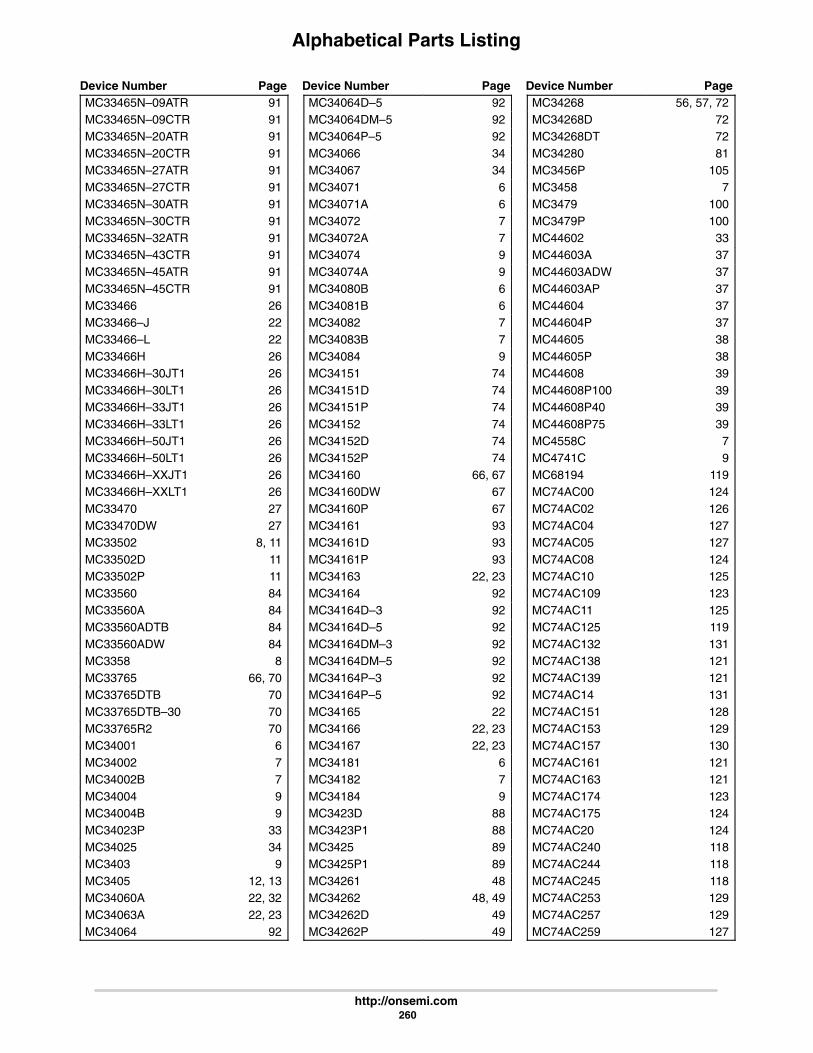
Alphabetical Parts Listing
Device Number Page Device Number Page Device Number Page
http://onsemi.com 260
MC33465N–09ATR 91MC33465N–09CTR 91MC33465N–20ATR 91MC33465N–20CTR 91MC33465N–27ATR 91MC33465N–27CTR 91MC33465N–30ATR 91MC33465N–30CTR 91MC33465N–32ATR 91MC33465N–43CTR 91MC33465N–45ATR 91MC33465N–45CTR 91MC33466 26MC33466–J 22MC33466–L 22MC33466H 26MC33466H–30JT1 26MC33466H–30LT1 26MC33466H–33JT1 26MC33466H–33LT1 26MC33466H–50JT1 26MC33466H–50LT1 26MC33466H–XXJT1 26MC33466H–XXLT1 26MC33470 27MC33470DW 27MC33502 8, 11MC33502D 11MC33502P 11MC33560 84MC33560A 84MC33560ADTB 84MC33560ADW 84MC3358 8MC33765 66, 70MC33765DTB 70MC33765DTB–30 70MC33765R2 70MC34001 6MC34002 7MC34002B 7MC34004 9MC34004B 9MC34023P 33MC34025 34MC3403 9MC3405 12, 13MC34060A 22, 32MC34063A 22, 23MC34064 92
MC34064D–5 92MC34064DM–5 92MC34064P–5 92MC34066 34MC34067 34MC34071 6MC34071A 6MC34072 7MC34072A 7MC34074 9MC34074A 9MC34080B 6MC34081B 6MC34082 7MC34083B 7MC34084 9MC34151 74MC34151D 74MC34151P 74MC34152 74MC34152D 74MC34152P 74MC34160 66, 67MC34160DW 67MC34160P 67MC34161 93MC34161D 93MC34161P 93MC34163 22, 23MC34164 92MC34164D–3 92MC34164D–5 92MC34164DM–3 92MC34164DM–5 92MC34164P–3 92MC34164P–5 92MC34165 22MC34166 22, 23MC34167 22, 23MC34181 6MC34182 7MC34184 9MC3423D 88MC3423P1 88MC3425 89MC3425P1 89MC34261 48MC34262 48, 49MC34262D 49MC34262P 49
MC34268 56, 57, 72MC34268D 72MC34268DT 72MC34280 81MC3456P 105MC3458 7MC3479 100MC3479P 100MC44602 33MC44603A 37MC44603ADW 37MC44603AP 37MC44604 37MC44604P 37MC44605 38MC44605P 38MC44608 39MC44608P100 39MC44608P40 39MC44608P75 39MC4558C 7MC4741C 9MC68194 119MC74AC00 124MC74AC02 126MC74AC04 127MC74AC05 127MC74AC08 124MC74AC10 125MC74AC109 123MC74AC11 125MC74AC125 119MC74AC132 131MC74AC138 121MC74AC139 121MC74AC14 131MC74AC151 128MC74AC153 129MC74AC157 130MC74AC161 121MC74AC163 121MC74AC174 123MC74AC175 124MC74AC20 124MC74AC240 118MC74AC244 118MC74AC245 118MC74AC253 129MC74AC257 129MC74AC259 127
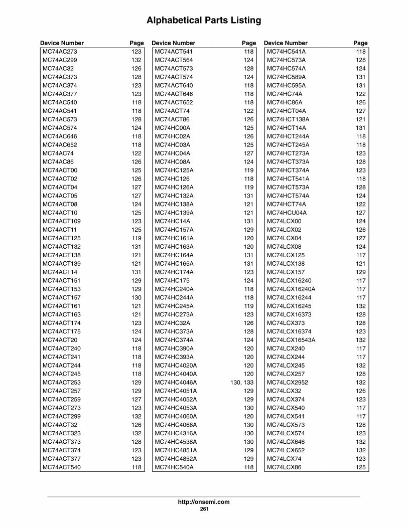
Alphabetical Parts Listing
Device Number Page Device Number Page Device Number Page
http://onsemi.com 261
MC74AC273 123MC74AC299 132MC74AC32 126MC74AC373 128MC74AC374 123MC74AC377 123MC74AC540 118MC74AC541 118MC74AC573 128MC74AC574 124MC74AC646 118MC74AC652 118MC74AC74 122MC74AC86 126MC74ACT00 125MC74ACT02 126MC74ACT04 127MC74ACT05 127MC74ACT08 124MC74ACT10 125MC74ACT109 123MC74ACT11 125MC74ACT125 119MC74ACT132 131MC74ACT138 121MC74ACT139 121MC74ACT14 131MC74ACT151 129MC74ACT153 129MC74ACT157 130MC74ACT161 121MC74ACT163 121MC74ACT174 123MC74ACT175 124MC74ACT20 124MC74ACT240 118MC74ACT241 118MC74ACT244 118MC74ACT245 118MC74ACT253 129MC74ACT257 129MC74ACT259 127MC74ACT273 123MC74ACT299 132MC74ACT32 126MC74ACT323 132MC74ACT373 128MC74ACT374 123MC74ACT377 123MC74ACT540 118
MC74ACT541 118MC74ACT564 124MC74ACT573 128MC74ACT574 124MC74ACT640 118MC74ACT646 118MC74ACT652 118MC74ACT74 122MC74ACT86 126MC74HC00A 125MC74HC02A 126MC74HC03A 125MC74HC04A 127MC74HC08A 124MC74HC125A 119MC74HC126 118MC74HC126A 119MC74HC132A 131MC74HC138A 121MC74HC139A 121MC74HC14A 131MC74HC157A 129MC74HC161A 120MC74HC163A 120MC74HC164A 131MC74HC165A 131MC74HC174A 123MC74HC175 124MC74HC240A 118MC74HC244A 118MC74HC245A 119MC74HC273A 123MC74HC32A 126MC74HC373A 128MC74HC374A 124MC74HC390A 120MC74HC393A 120MC74HC4020A 120MC74HC4040A 120MC74HC4046A 130, 133MC74HC4051A 129MC74HC4052A 129MC74HC4053A 130MC74HC4060A 120MC74HC4066A 130MC74HC4316A 130MC74HC4538A 130MC74HC4851A 129MC74HC4852A 129MC74HC540A 118
MC74HC541A 118MC74HC573A 128MC74HC574A 124MC74HC589A 131MC74HC595A 131MC74HC74A 122MC74HC86A 126MC74HCT04A 127MC74HCT138A 121MC74HCT14A 131MC74HCT244A 118MC74HCT245A 118MC74HCT273A 123MC74HCT373A 128MC74HCT374A 123MC74HCT541A 118MC74HCT573A 128MC74HCT574A 124MC74HCT74A 122MC74HCU04A 127MC74LCX00 124MC74LCX02 126MC74LCX04 127MC74LCX08 124MC74LCX125 117MC74LCX138 121MC74LCX157 129MC74LCX16240 117MC74LCX16240A 117MC74LCX16244 117MC74LCX16245 132MC74LCX16373 128MC74LCX373 128MC74LCX16374 123MC74LCX16543A 132MC74LCX240 117MC74LCX244 117MC74LCX245 132MC74LCX257 128MC74LCX2952 132MC74LCX32 126MC74LCX374 123MC74LCX540 117MC74LCX541 117MC74LCX573 128MC74LCX574 123MC74LCX646 132MC74LCX652 132MC74LCX74 123MC74LCX86 125
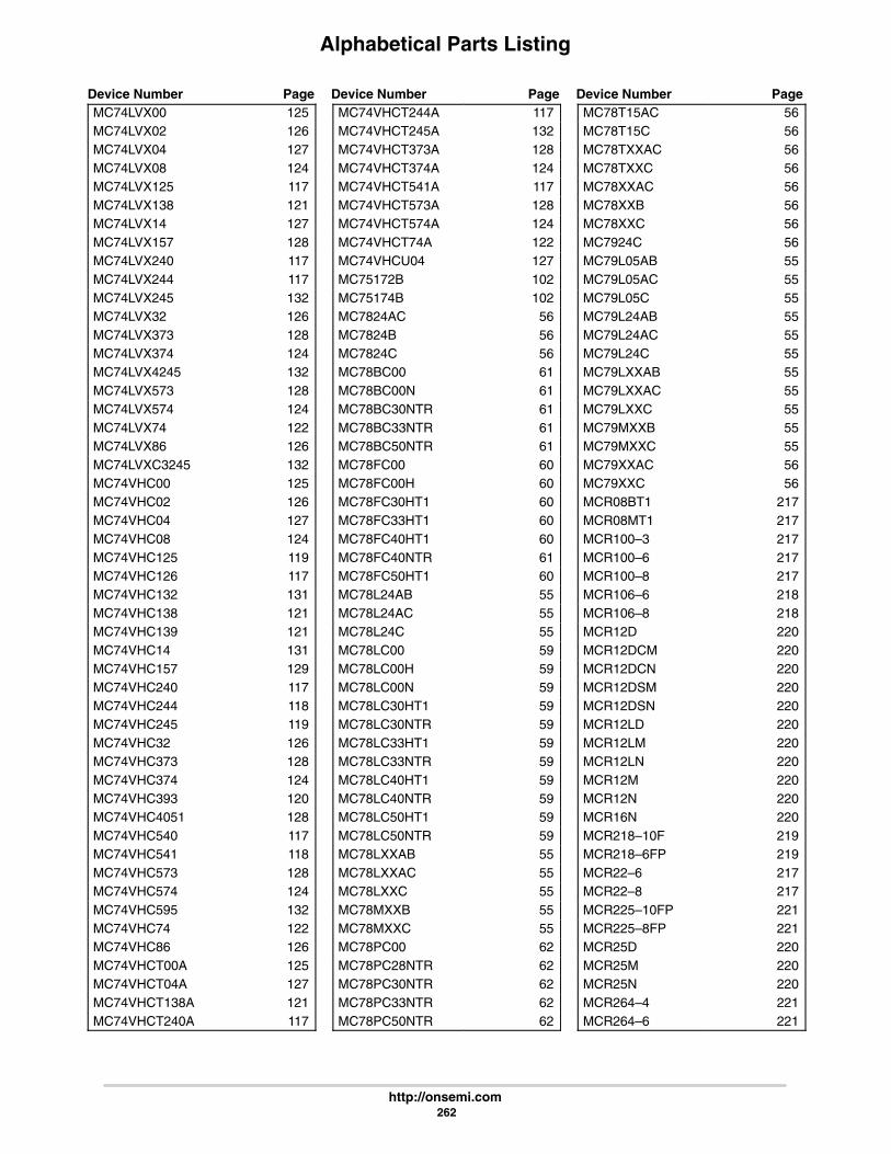
Alphabetical Parts Listing
Device Number Page Device Number Page Device Number Page
http://onsemi.com 262
MC74LVX00 125MC74LVX02 126MC74LVX04 127MC74LVX08 124MC74LVX125 117MC74LVX138 121MC74LVX14 127MC74LVX157 128MC74LVX240 117MC74LVX244 117MC74LVX245 132MC74LVX32 126MC74LVX373 128MC74LVX374 124MC74LVX4245 132MC74LVX573 128MC74LVX574 124MC74LVX74 122MC74LVX86 126MC74LVXC3245 132MC74VHC00 125MC74VHC02 126MC74VHC04 127MC74VHC08 124MC74VHC125 119MC74VHC126 117MC74VHC132 131MC74VHC138 121MC74VHC139 121MC74VHC14 131MC74VHC157 129MC74VHC240 117MC74VHC244 118MC74VHC245 119MC74VHC32 126MC74VHC373 128MC74VHC374 124MC74VHC393 120MC74VHC4051 128MC74VHC540 117MC74VHC541 118MC74VHC573 128MC74VHC574 124MC74VHC595 132MC74VHC74 122MC74VHC86 126MC74VHCT00A 125MC74VHCT04A 127MC74VHCT138A 121MC74VHCT240A 117
MC74VHCT244A 117MC74VHCT245A 132MC74VHCT373A 128MC74VHCT374A 124MC74VHCT541A 117MC74VHCT573A 128MC74VHCT574A 124MC74VHCT74A 122MC74VHCU04 127MC75172B 102MC75174B 102MC7824AC 56MC7824B 56MC7824C 56MC78BC00 61MC78BC00N 61MC78BC30NTR 61MC78BC33NTR 61MC78BC50NTR 61MC78FC00 60MC78FC00H 60MC78FC30HT1 60MC78FC33HT1 60MC78FC40HT1 60MC78FC40NTR 61MC78FC50HT1 60MC78L24AB 55MC78L24AC 55MC78L24C 55MC78LC00 59MC78LC00H 59MC78LC00N 59MC78LC30HT1 59MC78LC30NTR 59MC78LC33HT1 59MC78LC33NTR 59MC78LC40HT1 59MC78LC40NTR 59MC78LC50HT1 59MC78LC50NTR 59MC78LXXAB 55MC78LXXAC 55MC78LXXC 55MC78MXXB 55MC78MXXC 55MC78PC00 62MC78PC28NTR 62MC78PC30NTR 62MC78PC33NTR 62MC78PC50NTR 62
MC78T15AC 56MC78T15C 56MC78TXXAC 56MC78TXXC 56MC78XXAC 56MC78XXB 56MC78XXC 56MC7924C 56MC79L05AB 55MC79L05AC 55MC79L05C 55MC79L24AB 55MC79L24AC 55MC79L24C 55MC79LXXAB 55MC79LXXAC 55MC79LXXC 55MC79MXXB 55MC79MXXC 55MC79XXAC 56MC79XXC 56MCR08BT1 217MCR08MT1 217MCR100–3 217MCR100–6 217MCR100–8 217MCR106–6 218MCR106–8 218MCR12D 220MCR12DCM 220MCR12DCN 220MCR12DSM 220MCR12DSN 220MCR12LD 220MCR12LM 220MCR12LN 220MCR12M 220MCR12N 220MCR16N 220MCR218–10F 219MCR218–6FP 219MCR22–6 217MCR22–8 217MCR225–10FP 221MCR225–8FP 221MCR25D 220MCR25M 220MCR25N 220MCR264–4 221MCR264–6 221
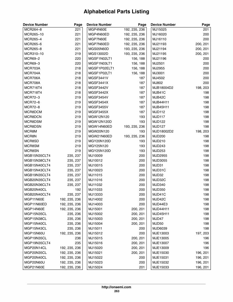
Alphabetical Parts Listing
Device Number Page Device Number Page Device Number Page
http://onsemi.com 263
MCR264–8 221MCR265–10 221MCR265–4 221MCR265–6 221MCR265–8 221MCR310–10 219MCR69–2 220MCR69–3 220MCR703A 218MCR704A 218MCR706A 218MCR708A 218MCR716T4 218MCR718T4 218MCR72–3 219MCR72–6 219MCR72–8 219MCR8DCM 219MCR8DCN 219MCR8DSM 219MCR8DSN 219MCR8M 219MCR8N 219MCR8SD 219MCR8SM 219MCR8SN 219MGB15N35CLT4 235, 237MGB15N38CLT4 235, 237MGB15N40CLT4 235, 237MGB15N43CLT4 235, 237MGB19N35CLT4 235, 237MGB20N35CLT4 235, 237MGB20N36CLT4 235, 237MGB20N40CL 192MGB20N40CLT4 235, 237MGP11N60E 192, 235, 236MGP11N60ED 192, 235, 236MGP14N60E 192, 235, 236MGP15N35CL 235, 236MGP15N38CL 235, 236MGP15N40CL 235, 236MGP15N43CL 235, 236MGP15N60U 192, 235, 236MGP19N35CL 236MGP19N35CLT4 235MGP20N14CL 192, 235, 236MGP20N35CL 192, 235, 236MGP20N40CL 192, 235, 236MGP20N60U 192, 235, 236MGP21N60E 192, 235, 236
MGP4N60E 192, 235, 236MGP4N60ED 192, 235, 236MGP7N60E 192, 235, 236MGP7N60ED 192, 235, 236MGS05N60D 193, 235, 236MGS13002D 193, 235, 236MGSF1N02LT1 156, 188MGSF1N03LT1 156, 188MGSF1P02ELT1 156, 188MGSF1P02LT1 156, 188MGSF3441V 187MGSF3441X 187MGSF3442V 187MGSF3442X 187MGSF3454V 187MGSF3454X 187MGSF3455V 187MGSF3455X 187MGW12N120 193MGW12N120D 193MGW14N60ED 193, 235, 236MGW20N120 193MGW21N60ED 193, 235, 236MGY20N120D 193MGY25N120 193MGY25N120D 193MJ10009 200MJ10012 200MJ10015 200MJ10023 200MJ11015 200MJ11016 200MJ11032 200MJ11033 200MJ13333 200MJ14002 200MJ14003 200MJ15001 200, 201MJ15002 200, 201MJ15003 200, 201MJ15004 200, 201MJ15011 200MJ15012 200MJ15015 200, 201MJ15016 200, 201MJ15020 200, 201MJ15021 200, 201MJ15022 200MJ15023 200MJ15024 201
MJ15025 201MJ16020 200MJ16110 200MJ21193 200, 201MJ21194 200, 201MJ21195 200, 201MJ21196 200MJ2501 200MJ2955 200MJ3001 200MJ4502 200MJ802 200MJB18004D2 198, 203MJB41C 198MJB42C 198MJB44H11 198MJB45H11 198MJD112 198MJD117 198MJD122 198MJD127 198MJD18002D2 198, 203MJD200 198MJD210 198MJD243 198MJD253 198MJD2955 198MJD3055 198MJD31 198MJD31C 198MJD32 198MJD32C 198MJD340 198MJD350 198MJD41C 198MJD42C 198MJD44E3 198MJD44H11 198MJD45H11 198MJD47 198MJD50 198MJD6039 198MJE13003 197, 203MJE13005 196MJE13007 196MJE13009 196MJE15030 196, 201MJE15031 196, 201MJE15032 196, 201MJE15033 196, 201
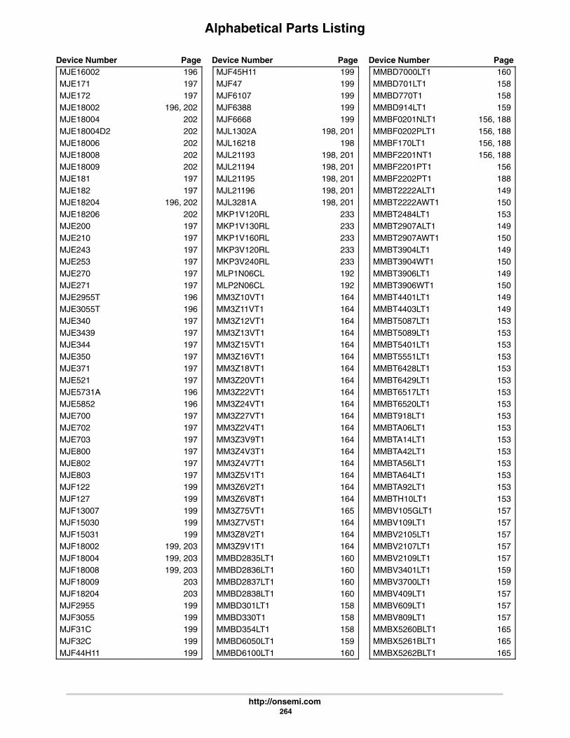
Alphabetical Parts Listing
Device Number Page Device Number Page Device Number Page
http://onsemi.com 264
MJE16002 196MJE171 197MJE172 197MJE18002 196, 202MJE18004 202MJE18004D2 202MJE18006 202MJE18008 202MJE18009 202MJE181 197MJE182 197MJE18204 196, 202MJE18206 202MJE200 197MJE210 197MJE243 197MJE253 197MJE270 197MJE271 197MJE2955T 196MJE3055T 196MJE340 197MJE3439 197MJE344 197MJE350 197MJE371 197MJE521 197MJE5731A 196MJE5852 196MJE700 197MJE702 197MJE703 197MJE800 197MJE802 197MJE803 197MJF122 199MJF127 199MJF13007 199MJF15030 199MJF15031 199MJF18002 199, 203MJF18004 199, 203MJF18008 199, 203MJF18009 203MJF18204 203MJF2955 199MJF3055 199MJF31C 199MJF32C 199MJF44H11 199
MJF45H11 199MJF47 199MJF6107 199MJF6388 199MJF6668 199MJL1302A 198, 201MJL16218 198MJL21193 198, 201MJL21194 198, 201MJL21195 198, 201MJL21196 198, 201MJL3281A 198, 201MKP1V120RL 233MKP1V130RL 233MKP1V160RL 233MKP3V120RL 233MKP3V240RL 233MLP1N06CL 192MLP2N06CL 192MM3Z10VT1 164MM3Z11VT1 164MM3Z12VT1 164MM3Z13VT1 164MM3Z15VT1 164MM3Z16VT1 164MM3Z18VT1 164MM3Z20VT1 164MM3Z22VT1 164MM3Z24VT1 164MM3Z27VT1 164MM3Z2V4T1 164MM3Z3V9T1 164MM3Z4V3T1 164MM3Z4V7T1 164MM3Z5V1T1 164MM3Z6V2T1 164MM3Z6V8T1 164MM3Z75VT1 165MM3Z7V5T1 164MM3Z8V2T1 164MM3Z9V1T1 164MMBD2835LT1 160MMBD2836LT1 160MMBD2837LT1 160MMBD2838LT1 160MMBD301LT1 158MMBD330T1 158MMBD354LT1 158MMBD6050LT1 159MMBD6100LT1 160
MMBD7000LT1 160MMBD701LT1 158MMBD770T1 158MMBD914LT1 159MMBF0201NLT1 156, 188MMBF0202PLT1 156, 188MMBF170LT1 156, 188MMBF2201NT1 156, 188MMBF2201PT1 156MMBF2202PT1 188MMBT2222ALT1 149MMBT2222AWT1 150MMBT2484LT1 153MMBT2907ALT1 149MMBT2907AWT1 150MMBT3904LT1 149MMBT3904WT1 150MMBT3906LT1 149MMBT3906WT1 150MMBT4401LT1 149MMBT4403LT1 149MMBT5087LT1 153MMBT5089LT1 153MMBT5401LT1 153MMBT5551LT1 153MMBT6428LT1 153MMBT6429LT1 153MMBT6517LT1 153MMBT6520LT1 153MMBT918LT1 153MMBTA06LT1 153MMBTA14LT1 153MMBTA42LT1 153MMBTA56LT1 153MMBTA64LT1 153MMBTA92LT1 153MMBTH10LT1 153MMBV105GLT1 157MMBV109LT1 157MMBV2105LT1 157MMBV2107LT1 157MMBV2109LT1 157MMBV3401LT1 159MMBV3700LT1 159MMBV409LT1 157MMBV609LT1 157MMBV809LT1 157MMBX5260BLT1 165MMBX5261BLT1 165MMBX5262BLT1 165

Alphabetical Parts Listing
Device Number Page Device Number Page Device Number Page
http://onsemi.com 265
MMBX5263BLT1 165MMBX5264BLT1 165MMBX5265BLT1 165MMBX5266BLT1 165MMBX5267BLT1 165MMBX5268BLT1 165MMBX5269BLT1 165MMBX5270BLT1 165MMBZ15VALT1 181MMBZ15VDLT1 181MMBZ20VALT1 181MMBZ27VCLT1 181MMBZ33VALT1 181MMBZ5221BLT1 164MMBZ5222BLT1 164MMBZ5223BLT1 164MMBZ5224BLT1 164MMBZ5225BLT1 164MMBZ5226BLT1 164MMBZ5227BLT1 164MMBZ5228BLT1 164MMBZ5229BLT1 164MMBZ5230BLT1 164MMBZ5231BLT1 164MMBZ5232BLT1 164MMBZ5233BLT1 164MMBZ5234BLT1 164MMBZ5235BLT1 164MMBZ5236BLT1 164MMBZ5237BLT1 164MMBZ5238BLT1 164MMBZ5239BLT1 164MMBZ5240BLT1 164MMBZ5241BLT1 164MMBZ5242BLT1 164MMBZ5243BLT1 164MMBZ5244BLT1 164MMBZ5245BLT1 164MMBZ5246BLT1 164MMBZ5247BLT1 164MMBZ5248BLT1 164MMBZ5249BLT1 164MMBZ5250BLT1 164MMBZ5251BLT1 164MMBZ5252BLT1 164MMBZ5253BLT1 164MMBZ5254BLT1 164MMBZ5255BLT1 164MMBZ5256BLT1 164MMBZ5257BLT1 164
MMBZ5258BLT1 164MMBZ5259BLT1 164MMBZ5V6ALT1 181MMBZ6V2ALT1 181MMBZ6V8ALT1 181MMDF1N05E 186MMDF2C01HD 186MMDF2C02E 186MMDF2C02HD 186MMDF2C03HD 186MMDF2N02E 186MMDF2N05Z 187MMDF2P01HD 186MMDF2P02E 186MMDF2P02HD 186MMDF2P03HD 186MMDF3N02HD 186MMDF3N03HD 186MMDF3N04HD 186MMDF3N06HD 186MMDF4C03HD 186MMDF4N01HD 186MMDF4P03HD 186MMDF6N02HD 186MMDF7N02Z 187MMDF7N03Z 187MMDFS6N303 186MMDJ3N03BJT 197MMDJ3P03BJT 197MMFT1N10E 187MMFT2955E 187MMFT2N02EL 187MMFT3055V 187MMFT3055VL 187MMFT5P03HD 187MMG05N60D 235, 237MMH0026 74MMJT9410 198MMJT9435 198MMQA12VT1 182MMQA12VT3 182MMQA13VT1 182MMQA13VT3 182MMQA15VT1 182MMQA15VT3 182MMQA18VT1 182MMQA18VT3 182MMQA20VT1 182MMQA20VT3 182MMQA21VT1 182
MMQA21VT3 182MMQA22VT1 182MMQA22VT3 182MMQA24VT1 182MMQA24VT3 182MMQA27VT1 182MMQA27VT3 182MMQA30VT1 182MMQA30VT3 182MMQA33VT1 182MMQA33VT3 182MMQA5V6T1 182MMQA5V6T3 182MMQA6V2T1 182MMQA6V2T3 182MMQA6V8T1 182MMQA6V8T3 182MMSD301T1 158MMSD71RKT1 159MMSD914T1 159MMSF10N02Z 187MMSF10N03Z 187MMSF3300 186MMSF3P02HD 186MMSF3P03HD 186MMSF4P01HD 186MMSF5N02HD 186MMSF5N03HD 186MMSF5P02HD 186MMSF7N03HD 186MMSZ10T1 164MMSZ11T1 164MMSZ12T1 164MMSZ13T1 164MMSZ15T1 164MMSZ16T1 164MMSZ18T1 164MMSZ20T1 164MMSZ22T1 164MMSZ24T1 164MMSZ27T1 164MMSZ2V4T1 164MMSZ2V7T1 164MMSZ30T1 164MMSZ33T1 164MMSZ36T1 164MMSZ39T1 164MMSZ3V0T1 164MMSZ3V3T1 164MMSZ3V6T1 164

Alphabetical Parts Listing
Device Number Page Device Number Page Device Number Page
http://onsemi.com 266
MMSZ3V9T1 164MMSZ43T1 165MMSZ4678T1 164MMSZ4679T1 164MMSZ4680T1 164MMSZ4681T1 164MMSZ4682T1 164MMSZ4683T1 164MMSZ4684T1 164MMSZ4685T1 164MMSZ4686T1 164MMSZ4687T1 164MMSZ4688T1 164MMSZ4689T1 164MMSZ4690T1 164MMSZ4691T1 164MMSZ4692T1 164MMSZ4693T1 164MMSZ4694T1 164MMSZ4695T1 164MMSZ4696T1 164MMSZ4697T1 164MMSZ4698T1 164MMSZ4699T1 164MMSZ4700T1 164MMSZ4701T1 164MMSZ4702T1 164MMSZ4703T1 164MMSZ4704T1 164MMSZ4705T1 164MMSZ4706T1 164MMSZ4707T1 164MMSZ4708T1 164MMSZ4709T1 164MMSZ4710T1 164MMSZ4711T1 164MMSZ4712T1 164MMSZ4713T1 164MMSZ4714T1 164MMSZ4715T1 164MMSZ4716T1 164MMSZ4717BT1 165MMSZ47T1 165MMSZ4V3T1 164MMSZ4V7T1 164MMSZ51T1 165MMSZ5221BT1 164MMSZ5222BT1 164MMSZ5223BT1 164MMSZ5224BT1 164
MMSZ5225BT1 164MMSZ5226BT1 164MMSZ5227BT1 164MMSZ5228BT1 164MMSZ5229BT1 164MMSZ5230BT1 164MMSZ5231BT1 164MMSZ5232BT1 164MMSZ5233BT1 164MMSZ5234BT1 164MMSZ5235BT1 164MMSZ5236BT1 164MMSZ5237BT1 164MMSZ5238BT1 164MMSZ5239BT1 164MMSZ5240BT1 164MMSZ5241BT1 164MMSZ5242BT1 164MMSZ5243BT1 164MMSZ5244BT1 164MMSZ5245BT1 164MMSZ5246BT1 164MMSZ5247BT1 164MMSZ5248BT1 164MMSZ5249BT1 164MMSZ5250BT1 164MMSZ5251BT1 164MMSZ5252BT1 164MMSZ5253BT1 164MMSZ5254BT1 164MMSZ5255BT1 164MMSZ5256BT1 164MMSZ5257BT1 164MMSZ5258BT1 164MMSZ5259BT1 164MMSZ5260BT1 165MMSZ5261BT1 165MMSZ5262BT1 165MMSZ5263BT1 165MMSZ5264BT1 165MMSZ5265BT1 165MMSZ5266BT1 165MMSZ5267BT1 165MMSZ5268BT1 165MMSZ5269BT1 165MMSZ5270BT1 165MMSZ56T1 165MMSZ5V1T1 164MMSZ5V6T1 164MMSZ62T1 165
MMSZ68T1 165MMSZ6V2T1 164MMSZ6V8T1 164MMSZ75T1 165MMSZ7V5T1 164MMSZ8V2T1 164MMSZ9V1T1 164MMT05B230T3 233MMT05B260T3 233MMT05B310T3 233MMT10B230T3 233MMT10B260T3 233MMT10B310T3 233MMUN2111LT1 151MMUN2112LT1 151MMUN2113LT1 151MMUN2114LT1 151MMUN2115LT1 151MMUN2116LT1 151MMUN2130LT1 151MMUN2131LT1 151MMUN2132LT1 151MMUN2133LT1 151MMUN2134LT1 151MMUN2211LT1 151MMUN2212LT1 151MMUN2213LT1 151MMUN2214LT1 151MMUN2215LT1 151MMUN2216LT1 151MMUN2230LT1 151MMUN2231LT1 151MMUN2232LT1 151MMUN2233LT1 151MMUN2234LT1 151MPF102 155MPF4392 155MPF4393 155MPN3404 159MPN3700 159MPS2222A 146MPS2907A 146MPS3563 148MPS3904 147MPS5179 148MPS651 147MPS6521 147MPS6523 147MPS6602 146MPS6652 146
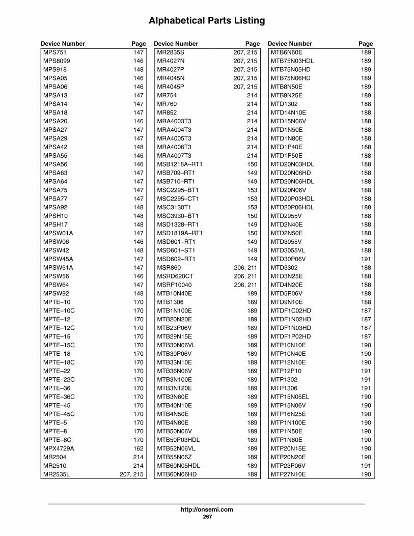
Alphabetical Parts Listing
Device Number Page Device Number Page Device Number Page
http://onsemi.com 267
MPS751 147MPS8099 146MPS918 148MPSA05 146MPSA06 146MPSA13 147MPSA14 147MPSA18 147MPSA20 146MPSA27 147MPSA29 147MPSA42 148MPSA55 146MPSA56 146MPSA63 147MPSA64 147MPSA75 147MPSA77 147MPSA92 148MPSH10 148MPSH17 148MPSW01A 147MPSW06 146MPSW42 148MPSW45A 147MPSW51A 147MPSW56 146MPSW64 147MPSW92 148MPTE–10 170MPTE–10C 170MPTE–12 170MPTE–12C 170MPTE–15 170MPTE–15C 170MPTE–18 170MPTE–18C 170MPTE–22 170MPTE–22C 170MPTE–36 170MPTE–36C 170MPTE–45 170MPTE–45C 170MPTE–5 170MPTE–8 170MPTE–8C 170MPX4729A 162MR2504 214MR2510 214MR2535L 207, 215
MR2835S 207, 215MR4027N 207, 215MR4027P 207, 215MR4045N 207, 215MR4045P 207, 215MR754 214MR760 214MR852 214MRA4003T3 214MRA4004T3 214MRA4005T3 214MRA4006T3 214MRA4007T3 214MSB1218A–RT1 150MSB709–RT1 149MSB710–RT1 149MSC2295–BT1 153MSC2295–CT1 153MSC3130T1 153MSC3930–BT1 150MSD1328–RT1 149MSD1819A–RT1 150MSD601–RT1 149MSD601–ST1 149MSD602–RT1 149MSR860 206, 211MSRD620CT 206, 211MSRP10040 206, 211MTB10N40E 189MTB1306 189MTB1N100E 189MTB20N20E 189MTB23P06V 189MTB29N15E 189MTB30N06VL 189MTB30P06V 189MTB33N10E 189MTB36N06V 189MTB3N100E 189MTB3N120E 189MTB3N60E 189MTB40N10E 189MTB4N50E 189MTB4N80E 189MTB50N06V 189MTB50P03HDL 189MTB52N06VL 189MTB55N06Z 189MTB60N05HDL 189MTB60N06HD 189
MTB6N60E 189MTB75N03HDL 189MTB75N05HD 189MTB75N06HD 189MTB8N50E 189MTB9N25E 189MTD1302 188MTD14N10E 188MTD15N06V 188MTD1N50E 188MTD1N80E 188MTD1P40E 188MTD1P50E 188MTD20N03HDL 188MTD20N06HD 188MTD20N06HDL 188MTD20N06V 188MTD20P03HDL 188MTD20P06HDL 188MTD2955V 188MTD2N40E 188MTD2N50E 188MTD3055V 188MTD3055VL 188MTD30P06V 191MTD3302 188MTD3N25E 188MTD4N20E 188MTD5P06V 188MTD9N10E 188MTDF1C02HD 187MTDF1N02HD 187MTDF1N03HD 187MTDF1P02HD 187MTP10N10E 190MTP10N40E 190MTP12N10E 190MTP12P10 191MTP1302 191MTP1306 191MTP15N05EL 190MTP15N06V 190MTP16N25E 190MTP1N100E 190MTP1N50E 190MTP1N60E 190MTP20N15E 190MTP20N20E 190MTP23P06V 191MTP27N10E 190
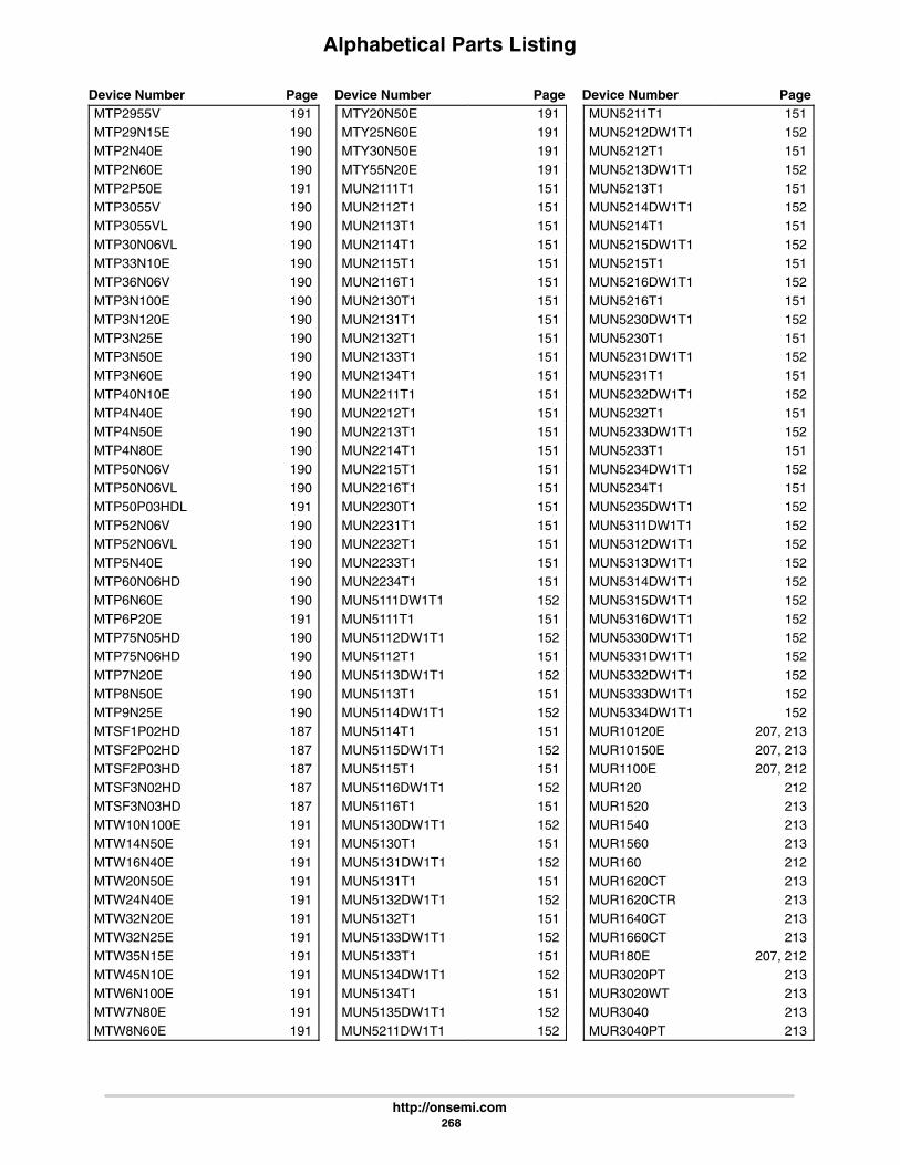
Alphabetical Parts Listing
Device Number Page Device Number Page Device Number Page
http://onsemi.com 268
MTP2955V 191MTP29N15E 190MTP2N40E 190MTP2N60E 190MTP2P50E 191MTP3055V 190MTP3055VL 190MTP30N06VL 190MTP33N10E 190MTP36N06V 190MTP3N100E 190MTP3N120E 190MTP3N25E 190MTP3N50E 190MTP3N60E 190MTP40N10E 190MTP4N40E 190MTP4N50E 190MTP4N80E 190MTP50N06V 190MTP50N06VL 190MTP50P03HDL 191MTP52N06V 190MTP52N06VL 190MTP5N40E 190MTP60N06HD 190MTP6N60E 190MTP6P20E 191MTP75N05HD 190MTP75N06HD 190MTP7N20E 190MTP8N50E 190MTP9N25E 190MTSF1P02HD 187MTSF2P02HD 187MTSF2P03HD 187MTSF3N02HD 187MTSF3N03HD 187MTW10N100E 191MTW14N50E 191MTW16N40E 191MTW20N50E 191MTW24N40E 191MTW32N20E 191MTW32N25E 191MTW35N15E 191MTW45N10E 191MTW6N100E 191MTW7N80E 191MTW8N60E 191
MTY20N50E 191MTY25N60E 191MTY30N50E 191MTY55N20E 191MUN2111T1 151MUN2112T1 151MUN2113T1 151MUN2114T1 151MUN2115T1 151MUN2116T1 151MUN2130T1 151MUN2131T1 151MUN2132T1 151MUN2133T1 151MUN2134T1 151MUN2211T1 151MUN2212T1 151MUN2213T1 151MUN2214T1 151MUN2215T1 151MUN2216T1 151MUN2230T1 151MUN2231T1 151MUN2232T1 151MUN2233T1 151MUN2234T1 151MUN5111DW1T1 152MUN5111T1 151MUN5112DW1T1 152MUN5112T1 151MUN5113DW1T1 152MUN5113T1 151MUN5114DW1T1 152MUN5114T1 151MUN5115DW1T1 152MUN5115T1 151MUN5116DW1T1 152MUN5116T1 151MUN5130DW1T1 152MUN5130T1 151MUN5131DW1T1 152MUN5131T1 151MUN5132DW1T1 152MUN5132T1 151MUN5133DW1T1 152MUN5133T1 151MUN5134DW1T1 152MUN5134T1 151MUN5135DW1T1 152MUN5211DW1T1 152
MUN5211T1 151MUN5212DW1T1 152MUN5212T1 151MUN5213DW1T1 152MUN5213T1 151MUN5214DW1T1 152MUN5214T1 151MUN5215DW1T1 152MUN5215T1 151MUN5216DW1T1 152MUN5216T1 151MUN5230DW1T1 152MUN5230T1 151MUN5231DW1T1 152MUN5231T1 151MUN5232DW1T1 152MUN5232T1 151MUN5233DW1T1 152MUN5233T1 151MUN5234DW1T1 152MUN5234T1 151MUN5235DW1T1 152MUN5311DW1T1 152MUN5312DW1T1 152MUN5313DW1T1 152MUN5314DW1T1 152MUN5315DW1T1 152MUN5316DW1T1 152MUN5330DW1T1 152MUN5331DW1T1 152MUN5332DW1T1 152MUN5333DW1T1 152MUN5334DW1T1 152MUR10120E 207, 213MUR10150E 207, 213MUR1100E 207, 212MUR120 212MUR1520 213MUR1540 213MUR1560 213MUR160 212MUR1620CT 213MUR1620CTR 213MUR1640CT 213MUR1660CT 213MUR180E 207, 212MUR3020PT 213MUR3020WT 213MUR3040 213MUR3040PT 213

Alphabetical Parts Listing
Device Number Page Device Number Page Device Number Page
http://onsemi.com 269
MUR3060PT 213MUR3060WT 213MUR3080 213MUR4100E 207, 212MUR420 212MUR460 212MUR480E 207, 212MUR5150E 207, 213MUR6040 213MUR620CT 213MUR8100E 207, 213MUR820 213MUR840 213MUR860 213MUR880E 207, 213MURB1620CT 212MURD320 212MURD620CT 212MURF1620CT 213MURH840CT 206, 213MURH860CT 206, 213MURHB840CT 206, 212MURHB860CT 206, 212MURHF860CT 206, 213MURP10020 214MURP10040 214MURP10060 214MURP20020CT 214MURP20040CT 214MURS120T3 212MURS160T3 212MURS320T3 212MURS360T3 212MV209 157MV2105 157MV2109 157MZP4728A 162MZP4730A 162MZP4731A 162MZP4732A 162MZP4733A 162MZP4734A 162MZP4735A 162MZP4736A 162MZP4737A 162MZP4738A 162MZP4739A 162MZP4740A 162MZP4741A 162MZP4742A 162
MZP4743A 162MZP4744A 162MZP4745A 162MZP4746A 162MZP4747A 162MZP4748A 162MZP4749A 162MZP4750A 163MZP4751A 163MZP4752A 163MZP4753A 163MZP4754A 163MZP4755A 163MZP4756A 163MZP4757A 163MZP4758A 163MZP4759A 163MZP4760A 163MZP4761A 163MZP4762A 163MZP4763A 163MZP4764A 163P2N2222A 148P2N2907A 148P6KE100A 168P6KE10A 168P6KE110A 168P6KE11A 168P6KE11CA 168P6KE120A 168P6KE12A 168P6KE130A 168P6KE13A 168P6KE150A 169P6KE15A 168P6KE160A 169P6KE16A 168P6KE170A 169P6KE180A 169P6KE18A 168P6KE200A 169P6KE20A 168P6KE22A 168P6KE24A 168P6KE27A 168P6KE30A 168P6KE33A 168P6KE36A 168P6KE39A 168P6KE43A 168
P6KE47A 168P6KE51A 168P6KE56A 168P6KE6.8A 168P6KE62A 168P6KE68A 168P6KE7.5A 168P6KE7.5CA 168P6KE75A 168P6KE8.2A 168P6KE82A 168P6KE9.1A 168P6KE91A 168P6SMB100AT3 177P6SMB10AT3 177P6SMB110AT3 177P6SMB11AT3 177P6SMB11CAT3 178P6SMB120AT3 177P6SMB12AT3 177P6SMB12CAT3 178P6SMB130AT3 177P6SMB13AT3 177P6SMB13CAT3 178P6SMB150AT3 177P6SMB15AT3 177P6SMB15CAT3 178P6SMB160AT3 177P6SMB16AT3 177P6SMB16CAT3 178P6SMB170AT3 177P6SMB180AT3 177P6SMB18AT3 177P6SMB18CAT3 178P6SMB200AT3 177P6SMB20AT3 177P6SMB20CAT3 178P6SMB22AT3 177P6SMB22CAT3 178P6SMB24AT3 177P6SMB24CAT3 178P6SMB27AT3 177P6SMB27CAT3 178P6SMB30AT3 177P6SMB30CAT3 178P6SMB33AT3 177P6SMB33CAT3 178P6SMB36AT3 177P6SMB36CAT3 178P6SMB39AT3 177
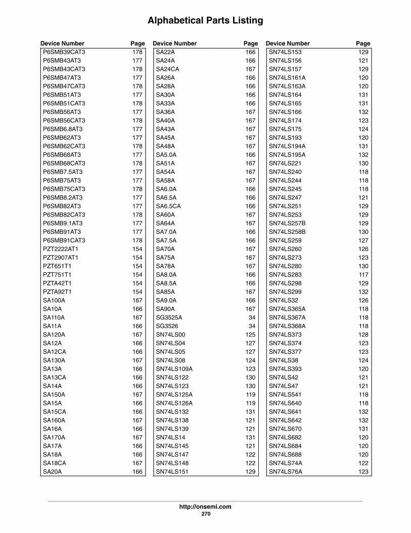
Alphabetical Parts Listing
Device Number Page Device Number Page Device Number Page
http://onsemi.com 270
P6SMB39CAT3 178P6SMB43AT3 177P6SMB43CAT3 178P6SMB47AT3 177P6SMB47CAT3 178P6SMB51AT3 177P6SMB51CAT3 178P6SMB56AT3 177P6SMB56CAT3 178P6SMB6.8AT3 177P6SMB62AT3 177P6SMB62CAT3 178P6SMB68AT3 177P6SMB68CAT3 178P6SMB7.5AT3 177P6SMB75AT3 177P6SMB75CAT3 178P6SMB8.2AT3 177P6SMB82AT3 177P6SMB82CAT3 178P6SMB9.1AT3 177P6SMB91AT3 177P6SMB91CAT3 178PZT2222AT1 154PZT2907AT1 154PZT651T1 154PZT751T1 154PZTA42T1 154PZTA92T1 154SA100A 167SA10A 166SA110A 167SA11A 166SA120A 167SA12A 166SA12CA 166SA130A 167SA13A 166SA13CA 166SA14A 166SA150A 167SA15A 166SA15CA 166SA160A 167SA16A 166SA170A 167SA17A 166SA18A 166SA18CA 167SA20A 166
SA22A 166SA24A 166SA24CA 167SA26A 166SA28A 166SA30A 166SA33A 166SA36A 167SA40A 167SA43A 167SA45A 167SA48A 167SA5.0A 166SA51A 167SA54A 167SA58A 167SA6.0A 166SA6.5A 166SA6.5CA 166SA60A 167SA64A 167SA7.0A 166SA7.5A 166SA70A 167SA75A 167SA78A 167SA8.0A 166SA8.5A 166SA85A 167SA9.0A 166SA90A 167SG3525A 34SG3526 34SN74LS00 125SN74LS04 127SN74LS05 127SN74LS08 124SN74LS109A 123SN74LS122 130SN74LS123 130SN74LS125A 119SN74LS126A 119SN74LS132 131SN74LS138 121SN74LS139 121SN74LS14 131SN74LS145 121SN74LS147 122SN74LS148 122SN74LS151 129
SN74LS153 129SN74LS156 121SN74LS157 129SN74LS161A 120SN74LS163A 120SN74LS164 131SN74LS165 131SN74LS166 132SN74LS174 123SN74LS175 124SN74LS193 120SN74LS194A 131SN74LS195A 132SN74LS221 130SN74LS240 118SN74LS244 118SN74LS245 118SN74LS247 121SN74LS251 129SN74LS253 129SN74LS257B 129SN74LS258B 130SN74LS259 127SN74LS260 126SN74LS273 123SN74LS280 130SN74LS283 117SN74LS298 129SN74LS299 132SN74LS32 126SN74LS365A 118SN74LS367A 118SN74LS368A 118SN74LS373 128SN74LS374 123SN74LS377 123SN74LS38 124SN74LS393 120SN74LS42 121SN74LS47 121SN74LS541 118SN74LS640 118SN74LS641 132SN74LS642 132SN74LS670 131SN74LS682 120SN74LS684 120SN74LS688 120SN74LS74A 122SN74LS76A 123
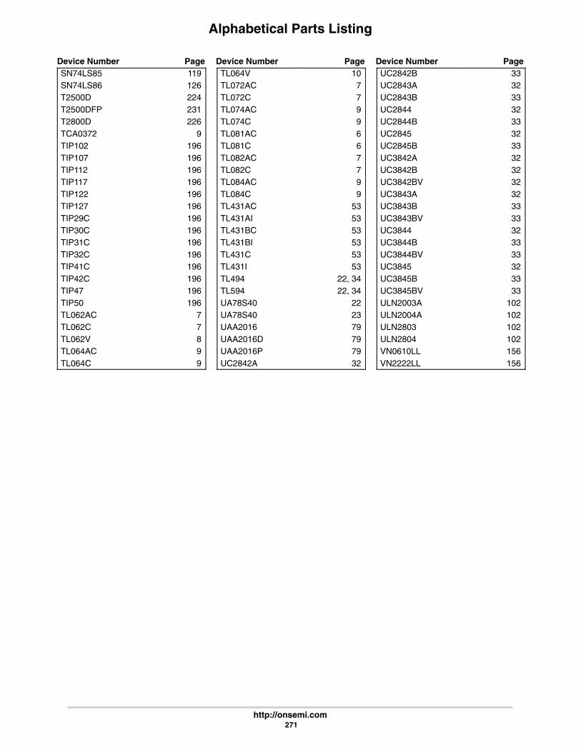
Alphabetical Parts Listing
Device Number Page Device Number Page Device Number Page
http://onsemi.com 271
SN74LS85 119SN74LS86 126T2500D 224T2500DFP 231T2800D 226TCA0372 9TIP102 196TIP107 196TIP112 196TIP117 196TIP122 196TIP127 196TIP29C 196TIP30C 196TIP31C 196TIP32C 196TIP41C 196TIP42C 196TIP47 196TIP50 196TL062AC 7TL062C 7TL062V 8TL064AC 9TL064C 9
TL064V 10TL072AC 7TL072C 7TL074AC 9TL074C 9TL081AC 6TL081C 6TL082AC 7TL082C 7TL084AC 9TL084C 9TL431AC 53TL431AI 53TL431BC 53TL431BI 53TL431C 53TL431I 53TL494 22, 34TL594 22, 34UA78S40 22UA78S40 23UAA2016 79UAA2016D 79UAA2016P 79UC2842A 32
UC2842B 33UC2843A 32UC2843B 33UC2844 32UC2844B 33UC2845 32UC2845B 33UC3842A 32UC3842B 32UC3842BV 32UC3843A 32UC3843B 33UC3843BV 33UC3844 32UC3844B 33UC3844BV 33UC3845 32UC3845B 33UC3845BV 33ULN2003A 102ULN2004A 102ULN2803 102ULN2804 102VN0610LL 156VN2222LL 156
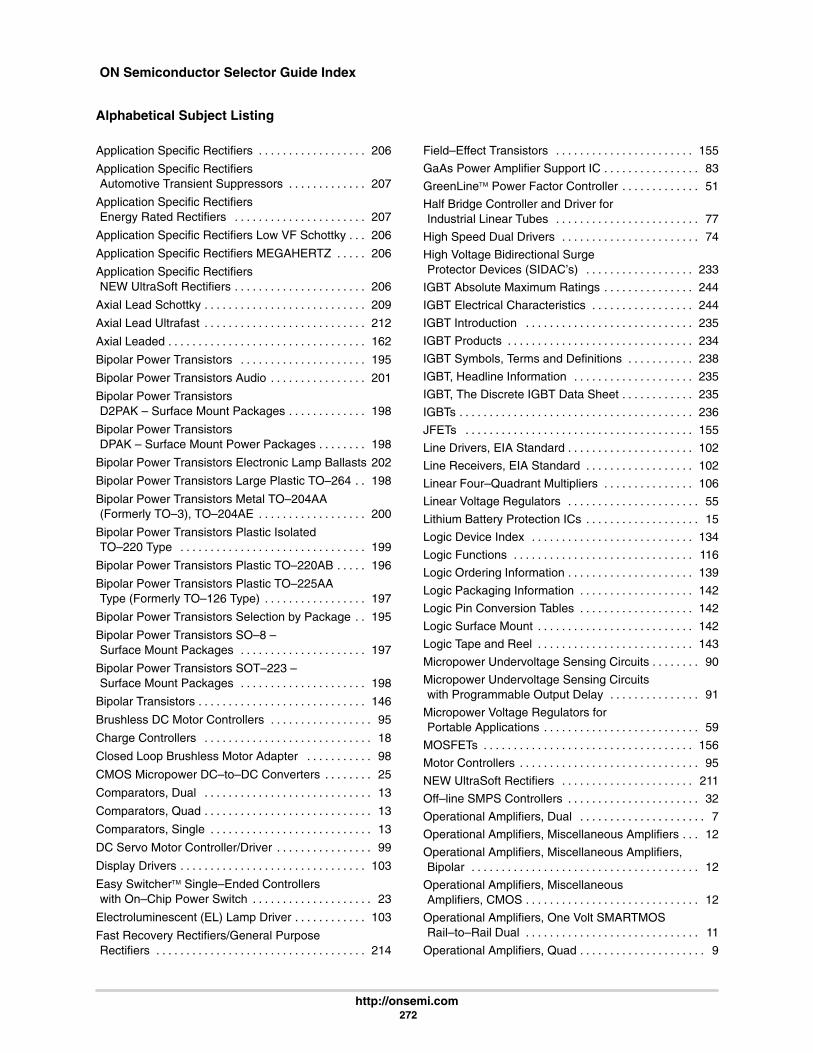
ON Semiconductor Selector Guide Index
http://onsemi.com 272
Alphabetical Subject Listing
Application Specific Rectifiers 206. . . . . . . . . . . . . . . . . .
Application Specific RectifiersAutomotive Transient Suppressors 207. . . . . . . . . . . . .
Application Specific Rectifiers Energy Rated Rectifiers 207. . . . . . . . . . . . . . . . . . . . . .
Application Specific Rectifiers Low VF Schottky 206. . .
Application Specific Rectifiers MEGAHERTZ 206. . . . .
Application Specific Rectifiers NEW UltraSoft Rectifiers 206. . . . . . . . . . . . . . . . . . . . . .
Axial Lead Schottky 209. . . . . . . . . . . . . . . . . . . . . . . . . . .
Axial Lead Ultrafast 212. . . . . . . . . . . . . . . . . . . . . . . . . . .
Axial Leaded 162. . . . . . . . . . . . . . . . . . . . . . . . . . . . . . . . .
Bipolar Power Transistors 195. . . . . . . . . . . . . . . . . . . . .
Bipolar Power Transistors Audio 201. . . . . . . . . . . . . . . .
Bipolar Power Transistors D2PAK – Surface Mount Packages 198. . . . . . . . . . . . .
Bipolar Power Transistors DPAK – Surface Mount Power Packages 198. . . . . . . .
Bipolar Power Transistors Electronic Lamp Ballasts 202
Bipolar Power Transistors Large Plastic TO–264 198. .
Bipolar Power Transistors Metal TO–204AA (Formerly TO–3), TO–204AE 200. . . . . . . . . . . . . . . . . .
Bipolar Power Transistors Plastic Isolated TO–220 Type 199. . . . . . . . . . . . . . . . . . . . . . . . . . . . . . .
Bipolar Power Transistors Plastic TO–220AB 196. . . . .
Bipolar Power Transistors Plastic TO–225AAType (Formerly TO–126 Type) 197. . . . . . . . . . . . . . . . .
Bipolar Power Transistors Selection by Package 195. .
Bipolar Power Transistors SO–8 – Surface Mount Packages 197. . . . . . . . . . . . . . . . . . . . .
Bipolar Power Transistors SOT–223 – Surface Mount Packages 198. . . . . . . . . . . . . . . . . . . . .
Bipolar Transistors 146. . . . . . . . . . . . . . . . . . . . . . . . . . . .
Brushless DC Motor Controllers 95. . . . . . . . . . . . . . . . .
Charge Controllers 18. . . . . . . . . . . . . . . . . . . . . . . . . . . .
Closed Loop Brushless Motor Adapter 98. . . . . . . . . . .
CMOS Micropower DC–to–DC Converters 25. . . . . . . .
Comparators, Dual 13. . . . . . . . . . . . . . . . . . . . . . . . . . . .
Comparators, Quad 13. . . . . . . . . . . . . . . . . . . . . . . . . . . .
Comparators, Single 13. . . . . . . . . . . . . . . . . . . . . . . . . . .
DC Servo Motor Controller/Driver 99. . . . . . . . . . . . . . . .
Display Drivers 103. . . . . . . . . . . . . . . . . . . . . . . . . . . . . . .
Easy Switcher Single–Ended Controllers with On–Chip Power Switch 23. . . . . . . . . . . . . . . . . . . .
Electroluminescent (EL) Lamp Driver 103. . . . . . . . . . . .
Fast Recovery Rectifiers/General Purpose Rectifiers 214. . . . . . . . . . . . . . . . . . . . . . . . . . . . . . . . . . .
Field–Effect Transistors 155. . . . . . . . . . . . . . . . . . . . . . .
GaAs Power Amplifier Support IC 83. . . . . . . . . . . . . . . .
GreenLine Power Factor Controller 51. . . . . . . . . . . . .
Half Bridge Controller and Driver for Industrial Linear Tubes 77. . . . . . . . . . . . . . . . . . . . . . . .
High Speed Dual Drivers 74. . . . . . . . . . . . . . . . . . . . . . .
High Voltage Bidirectional Surge Protector Devices (SIDAC’s) 233. . . . . . . . . . . . . . . . . .
IGBT Absolute Maximum Ratings 244. . . . . . . . . . . . . . .
IGBT Electrical Characteristics 244. . . . . . . . . . . . . . . . .
IGBT Introduction 235. . . . . . . . . . . . . . . . . . . . . . . . . . . .
IGBT Products 234. . . . . . . . . . . . . . . . . . . . . . . . . . . . . . .
IGBT Symbols, Terms and Definitions 238. . . . . . . . . . .
IGBT, Headline Information 235. . . . . . . . . . . . . . . . . . . .
IGBT, The Discrete IGBT Data Sheet 235. . . . . . . . . . . .
IGBTs 236. . . . . . . . . . . . . . . . . . . . . . . . . . . . . . . . . . . . . . .
JFETs 155. . . . . . . . . . . . . . . . . . . . . . . . . . . . . . . . . . . . . .
Line Drivers, EIA Standard 102. . . . . . . . . . . . . . . . . . . . .
Line Receivers, EIA Standard 102. . . . . . . . . . . . . . . . . .
Linear Four–Quadrant Multipliers 106. . . . . . . . . . . . . . .
Linear Voltage Regulators 55. . . . . . . . . . . . . . . . . . . . . .
Lithium Battery Protection ICs 15. . . . . . . . . . . . . . . . . . .
Logic Device Index 134. . . . . . . . . . . . . . . . . . . . . . . . . . .
Logic Functions 116. . . . . . . . . . . . . . . . . . . . . . . . . . . . . .
Logic Ordering Information 139. . . . . . . . . . . . . . . . . . . . .
Logic Packaging Information 142. . . . . . . . . . . . . . . . . . .
Logic Pin Conversion Tables 142. . . . . . . . . . . . . . . . . . .
Logic Surface Mount 142. . . . . . . . . . . . . . . . . . . . . . . . . .
Logic Tape and Reel 143. . . . . . . . . . . . . . . . . . . . . . . . . .
Micropower Undervoltage Sensing Circuits 90. . . . . . . .
Micropower Undervoltage Sensing Circuits with Programmable Output Delay 91. . . . . . . . . . . . . . .
Micropower Voltage Regulators for Portable Applications 59. . . . . . . . . . . . . . . . . . . . . . . . . .
MOSFETs 156. . . . . . . . . . . . . . . . . . . . . . . . . . . . . . . . . . .
Motor Controllers 95. . . . . . . . . . . . . . . . . . . . . . . . . . . . . .
NEW UltraSoft Rectifiers 211. . . . . . . . . . . . . . . . . . . . . .
Off–line SMPS Controllers 32. . . . . . . . . . . . . . . . . . . . . .
Operational Amplifiers, Dual 7. . . . . . . . . . . . . . . . . . . . .
Operational Amplifiers, Miscellaneous Amplifiers 12. . .
Operational Amplifiers, Miscellaneous Amplifiers, Bipolar 12. . . . . . . . . . . . . . . . . . . . . . . . . . . . . . . . . . . . . .
Operational Amplifiers, Miscellaneous Amplifiers, CMOS 12. . . . . . . . . . . . . . . . . . . . . . . . . . . . .
Operational Amplifiers, One Volt SMARTMOS Rail–to–Rail Dual 11. . . . . . . . . . . . . . . . . . . . . . . . . . . . .
Operational Amplifiers, Quad 9. . . . . . . . . . . . . . . . . . . . .
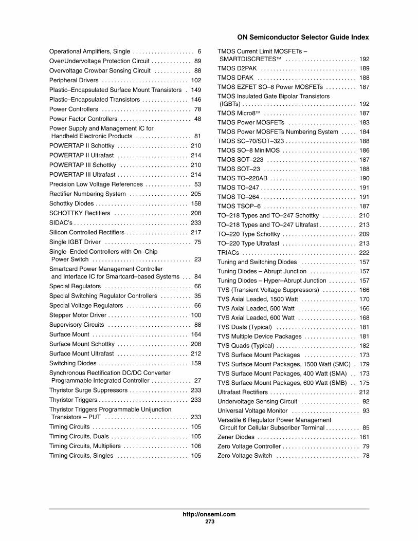
ON Semiconductor Selector Guide Index
http://onsemi.com 273
Operational Amplifiers, Single 6. . . . . . . . . . . . . . . . . . . .
Over/Undervoltage Protection Circuit 89. . . . . . . . . . . . .
Overvoltage Crowbar Sensing Circuit 88. . . . . . . . . . . .
Peripheral Drivers 102. . . . . . . . . . . . . . . . . . . . . . . . . . . .
Plastic–Encapsulated Surface Mount Transistors 149.
Plastic–Encapsulated Transistors 146. . . . . . . . . . . . . . .
Power Controllers 78. . . . . . . . . . . . . . . . . . . . . . . . . . . . .
Power Factor Controllers 48. . . . . . . . . . . . . . . . . . . . . . .
Power Supply and Management IC for Handheld Electronic Products 81. . . . . . . . . . . . . . . . . .
POWERTAP II Schottky 210. . . . . . . . . . . . . . . . . . . . . . .
POWERTAP II Ultrafast 214. . . . . . . . . . . . . . . . . . . . . . .
POWERTAP III Schottky 210. . . . . . . . . . . . . . . . . . . . . .
POWERTAP III Ultrafast 214. . . . . . . . . . . . . . . . . . . . . . .
Precision Low Voltage References 53. . . . . . . . . . . . . . .
Rectifier Numbering System 205. . . . . . . . . . . . . . . . . . .
Schottky Diodes 158. . . . . . . . . . . . . . . . . . . . . . . . . . . . . .
SCHOTTKY Rectifiers 208. . . . . . . . . . . . . . . . . . . . . . . .
SIDAC’s 233. . . . . . . . . . . . . . . . . . . . . . . . . . . . . . . . . . . . .
Silicon Controlled Rectifiers 217. . . . . . . . . . . . . . . . . . . .
Single IGBT Driver 75. . . . . . . . . . . . . . . . . . . . . . . . . . . .
Single–Ended Controllers with On–Chip Power Switch 23. . . . . . . . . . . . . . . . . . . . . . . . . . . . . . . .
Smartcard Power Management Controller and Interface IC for Smartcard–based Systems 84. . .
Special Regulators 66. . . . . . . . . . . . . . . . . . . . . . . . . . . .
Special Switching Regulator Controllers 35. . . . . . . . . .
Special Voltage Regulators 66. . . . . . . . . . . . . . . . . . . . .
Stepper Motor Driver 100. . . . . . . . . . . . . . . . . . . . . . . . . .
Supervisory Circuits 88. . . . . . . . . . . . . . . . . . . . . . . . . . .
Surface Mount 164. . . . . . . . . . . . . . . . . . . . . . . . . . . . . . .
Surface Mount Schottky 208. . . . . . . . . . . . . . . . . . . . . . .
Surface Mount Ultrafast 212. . . . . . . . . . . . . . . . . . . . . . .
Switching Diodes 159. . . . . . . . . . . . . . . . . . . . . . . . . . . . .
Synchronous Rectification DC/DC Converter Programmable Integrated Controller 27. . . . . . . . . . . . .
Thyristor Surge Suppressors 233. . . . . . . . . . . . . . . . . . .
Thyristor Triggers 233. . . . . . . . . . . . . . . . . . . . . . . . . . . . .
Thyristor Triggers Programmable Unijunction Transistors – PUT 233. . . . . . . . . . . . . . . . . . . . . . . . . . .
Timing Circuits 105. . . . . . . . . . . . . . . . . . . . . . . . . . . . . . .
Timing Circuits, Duals 105. . . . . . . . . . . . . . . . . . . . . . . . .
Timing Circuits, Multipliers 106. . . . . . . . . . . . . . . . . . . . .
Timing Circuits, Singles 105. . . . . . . . . . . . . . . . . . . . . . .
TMOS Current Limit MOSFETs – SMARTDISCRETES 192. . . . . . . . . . . . . . . . . . . . . . .
TMOS D2PAK 189. . . . . . . . . . . . . . . . . . . . . . . . . . . . . . .
TMOS DPAK 188. . . . . . . . . . . . . . . . . . . . . . . . . . . . . . . .
TMOS EZFET SO–8 Power MOSFETs 187. . . . . . . . . .
TMOS Insulated Gate Bipolar Transistors (IGBTs) 192. . . . . . . . . . . . . . . . . . . . . . . . . . . . . . . . . . . . .
TMOS Micro8 187. . . . . . . . . . . . . . . . . . . . . . . . . . . . . .
TMOS Power MOSFETs 183. . . . . . . . . . . . . . . . . . . . . .
TMOS Power MOSFETs Numbering System 184. . . . .
TMOS SC–70/SOT–323 188. . . . . . . . . . . . . . . . . . . . . . .
TMOS SO–8 MiniMOS 186. . . . . . . . . . . . . . . . . . . . . . . .
TMOS SOT–223 187. . . . . . . . . . . . . . . . . . . . . . . . . . . . .
TMOS SOT–23 188. . . . . . . . . . . . . . . . . . . . . . . . . . . . . .
TMOS TO–220AB 190. . . . . . . . . . . . . . . . . . . . . . . . . . . .
TMOS TO–247 191. . . . . . . . . . . . . . . . . . . . . . . . . . . . . . .
TMOS TO–264 191. . . . . . . . . . . . . . . . . . . . . . . . . . . . . . .
TMOS TSOP–6 187. . . . . . . . . . . . . . . . . . . . . . . . . . . . . .
TO–218 Types and TO–247 Schottky 210. . . . . . . . . . .
TO–218 Types and TO–247 Ultrafast 213. . . . . . . . . . . .
TO–220 Type Schottky 209. . . . . . . . . . . . . . . . . . . . . . . .
TO–220 Type Ultrafast 213. . . . . . . . . . . . . . . . . . . . . . . .
TRIACs 222. . . . . . . . . . . . . . . . . . . . . . . . . . . . . . . . . . . . .
Tuning and Switching Diodes 157. . . . . . . . . . . . . . . . . .
Tuning Diodes – Abrupt Junction 157. . . . . . . . . . . . . . .
Tuning Diodes – Hyper–Abrupt Junction 157. . . . . . . . .
TVS (Transient Voltage Suppressors) 166. . . . . . . . . . .
TVS Axial Leaded, 1500 Watt 170. . . . . . . . . . . . . . . . . .
TVS Axial Leaded, 500 Watt 166. . . . . . . . . . . . . . . . . . .
TVS Axial Leaded, 600 Watt 168. . . . . . . . . . . . . . . . . . .
TVS Duals (Typical) 181. . . . . . . . . . . . . . . . . . . . . . . . . .
TVS Multiple Device Packages 181. . . . . . . . . . . . . . . . .
TVS Quads (Typical) 182. . . . . . . . . . . . . . . . . . . . . . . . . .
TVS Surface Mount Packages 173. . . . . . . . . . . . . . . . .
TVS Surface Mount Packages, 1500 Watt (SMC) 179.
TVS Surface Mount Packages, 400 Watt (SMA) 173. .
TVS Surface Mount Packages, 600 Watt (SMB) 175. .
Ultrafast Rectifiers 212. . . . . . . . . . . . . . . . . . . . . . . . . . . .
Undervoltage Sensing Circuit 92. . . . . . . . . . . . . . . . . . .
Universal Voltage Monitor 93. . . . . . . . . . . . . . . . . . . . . .
Versatile 6 Regulator Power Management Circuit for Cellular Subscriber Terminal 85. . . . . . . . . . .
Zener Diodes 161. . . . . . . . . . . . . . . . . . . . . . . . . . . . . . . .
Zero Voltage Controller 79. . . . . . . . . . . . . . . . . . . . . . . . .
Zero Voltage Switch 78. . . . . . . . . . . . . . . . . . . . . . . . . . .

ON Semiconductor Selector Guide
http://onsemi.com 274
ON SEMICONDUCTOR WORLDWIDE SALES OFFICESUNITED STATES
ALABAMAHuntsville (256)464–6800. . . . . . . . . . . . . . .
CALIFORNIAIrvine (949)753–7360. . . . . . . . . . . . . . . . . . . San Jose (408)749–0510. . . . . . . . . . . . . . .
COLORADODenver (303)337–3434. . . . . . . . . . . . . . . . .
FLORIDASt. Petersberg (813)524–4177. . . . . . . . . . .
GEORGIAAtlanta (770)729–7100. . . . . . . . . . . . . . . . .
ILLINOISChicago (847)413–2500. . . . . . . . . . . . . . . .
MASSACHUSETTSBoston (781)932–9700. . . . . . . . . . . . . . . . .
MICHIGANDetroit (248)347–6800. . . . . . . . . . . . . . . . . .
MINNESOTAMinnetonka (612)932–1500. . . . . . . . . . . . .
NORTH CAROLINARaleigh (919)870–4355. . . . . . . . . . . . . . . . .
PENNSYLVANIAPhiladelphia/Horsham (215)957–4100. . . .
TEXASDallas (972)516–5100. . . . . . . . . . . . . . . . . .
CANADAONTARIO
Ottawa (613)226–3491. . . . . . . . . . . . . . . . . QUEBEC
Montreal (514)333–3300. . . . . . . . . . . . . . . .
INTERNATIONALBRAZIL
Sao Paulo 55(011)3030–5244. . . . . . . . . . . CHINA
Beijing 86–10–65642288. . . . . . . . . . . . . . . . Guangzhou 86–20–87537888. . . . . . . . . . . Shanghai 86–21–63747668. . . . . . . . . . . . .
FRANCEParis 33134 635900. . . . . . . . . . . . . . . . . . . .
GERMANYMunich 49 89 92103–0. . . . . . . . . . . . . . . . .
HONG KONGHong Kong 852–2–610–6888. . . . . . . . . . . .
INDIABangalore 91–80–5598615. . . . . . . . . . . . . .
ISRAELTel Aviv 972–9–9522333. . . . . . . . . . . . . . . .
ITALYMilan 39(2)82201. . . . . . . . . . . . . . . . . . . . . .
JAPANTokyo 81–3–5487–8345. . . . . . . . . . . . . . . .
INTERNATIONAL (continued)KOREA
Seoul 82–2–3440–7200. . . . . . . . . . . . . . . . . MALAYSIA
Penang 60(4)228–2514. . . . . . . . . . . . . . . . . MEXICO
Guadalajara 52(36)78–0750. . . . . . . . . . . . . PHILIPPINES
Manila (63)2 807–8455. . . . . . . . . . . . . . . . . . PUERTO RICO
San Juan (787)641–4100. . . . . . . . . . . . . . . SINGAPORE
Singapore (65)4818188. . . . . . . . . . . . . . . . . SPAIN
Madrid 34(1)457–8204. . . . . . . . . . . . . . . . . . or 34(1)457–8254. . . . . . . . . . . . . . . . . . . . . .
SWEDENStockholm 46(8)734–8800. . . . . . . . . . . . . .
TAIWANTaipei 886(2)27058000. . . . . . . . . . . . . . . . .
THAILANDBangkok 66(2)254–4910. . . . . . . . . . . . . . . .
UNITED KINGDOMAylesbury 44 1 (296)395252. . . . . . . . . . . . .

ON Semiconductor Selector Guide
http://onsemi.com 275
MOTOROLA SPS STANDARD DOCUMENT TYPE DEFINITIONS
REFERENCE MANUAL
A Reference Manual is a publication that contains a comprehensive system or device–specific description of the structure andfunction (operation) of a particular part/system; used overwhelmingly to describe the functionality of a microprocessor,microcontroller, or some other sub–micron sized device. Procedural information in a Reference Manual is limited to less than 40percent (usually much less).
USER’S GUIDE
A User’s Guide contains procedural, task–oriented instructions for using or running a device or product. A User’s Guide differsfrom a Reference Manual in the following respects:* Majority of information (> 60%) is procedural, not functional, in nature* Volume of information is typically less than for Reference Manuals* Usually written more in active voice, using second–person singular (you) than is found in Reference Manuals* May contain photographs and detailed line drawings rather than simple illustrations that are often found in Reference Manuals
POCKET GUIDE
A Pocket Guide is a pocket–sized document that contains technical reference information. Types of information commonly foundin pocket guides include block diagrams, pinouts, alphabetized instruction set, alphabetized registers, alphabetized third–partyvendors and their products, etc.
ADDENDUM
A documentation Addendum is a supplemental publication that contains missing information or replaces preliminary informationin the primary publication it supports. Individual addendum items are published cumulatively. Addendums end with the next revisionof the primary document.
APPLICATION NOTE
An Application Note is a document that contains real–world application information about how a specific Motoroladevice/product is used with other Motorola or vendor parts/software to address a particular technical issue. Parts and/or software mustalready exist and be available.
A document called “Application–Specific Information” is not the same as an Application Note.
SELECTOR GUIDE
A Selector Guide is a tri–fold (or larger) document published on a regular basis (usually quarterly) by many, if not all, divisions,that contains key line–item, device–specific information for particular product families. Some Selector Guides are published in bookformat and contain previously published information.
PRODUCT PREVIEW
A Product Preview is a summary document for a product/device under consideration or in the early stages of development. TheProduct Preview exists only until an “Advance Information” document is published that replaces it. The Product Preview is oftenused as the first section or chapter in a corresponding reference manual. The Product Preview displays the following disclaimer atthe bottom of the first page: “Motorola reserves the right to change or discontinue this product without notice.”
ADVANCE INFORMATION
The Advance Information document is for a device that is NOT fully MC–qualified. The Advance Information document isreplaced with the Technical Data document once the device/part becomes fully MC–qualified. The Advance Information documentdisplays the following disclaimer at the bottom of the first page: “This document contains information on a new product.Specifications and information herein are subject to change without notice.”
TECHNICAL DATA
The Technical Data document is for a product/device that is in full production (i.e., fully released). It replaces the AdvanceInformation document and represents a part that is M, X, XC, or MC qualified. The Technical Data document is virtually the samedocument as the Product Preview and the Advance Information document with the exception that it provides information that isunavailable for a product in the early phases of development (such as complete parametric characterization data). The Technical Datadocument is also a more comprehensive document that either of its earlier incarnations. This document displays no disclaimer, andwhile it may be informally referred to as a “data sheet,” it is not labeled as such.
ENGINEERING BULLETIN
An Engineering Bulletin is a writeup that typically focuses on a single specific solution for a particular engineering orprogramming issue involving one or several devices.

SG388/DRev. 1, Aug-1999
Master ComponentsSelector Guide
ON SemiconductorFormerly a Division of Motorola
ON Semiconductor and are trademarks of Semiconductor Components Industries, LLC (SCILLC). SCILLC reserves the right to make changes without further notice to any products herein. SCILLC makes no warranty, representation or guarantee regarding the suitability of its products for any particular purpose, nor does SCILLC assume any liability arising out of the application or use of any product or circuit, and specifically disclaims any and all liability, including without limitation special, consequential or incidental damages. “Typical” parameters which may be provided in SCILLC data sheets and/or specifications can and do vary in different applications and actual performance may vary over time. All operating parameters, including “Typicals” must be validated for each customer application by customer’s technical experts. SCILLC does not convey any license under its patent rights nor the rights of others. SCILLC products are not designed, intended, or authorized for use as components in systems intended for surgical implant into the body, or other applications intended to support or sustain life, or for any other application in which the failure of the SCILLC product could create a situation where personal injury or death may occur. Should Buyer purchase or use SCILLC products for any such unintended or unauthorized application, Buyer shall indemnify and hold SCILLC and its officers, employees, subsidiaries, affiliates, and distributors harmless against all claims, costs, damages, and expenses, and reasonable attorney fees arising out of, directly or indirectly, any claim of personal injury or death associated with such unintended or unauthorized use, even if such claim alleges that SCILLC was negligent regarding the design or manufacture of the part. SCILLC is an Equal Opportunity/Affirmative Action Employer.
USA/EUROPE Literature Fulfillment:Literature Distribution Center for ON SemiconductorP.O. Box 5193, Denver, Colorado 80217 USAPhone: 303-675-2175 or 800-344-3860 Toll Free USA/CanadaFax: 303-675-2176 or 800-344-3867 Toll Free USA/CanadaEmail: [email protected]
Fax Response Line: 303-675-2167800-344-3810 Toll Free USA/Canada
N. Amercian Technical Support: 800-282-9855 Toll Free USA/Canada
ASIA/PACIFIC: LDC for ON Semiconductor - Asia SupportPhone: 303-675-2121 (Tue-Fri 9:00am to 1:00pm Hong Kong Time)Email: [email protected]
JAPAN: ON Semiconductor, Japan Customer Focus Center4-32-1 Nishi-Gotanda, Shinagawa-ku, Tokyo, Japan 141-8549Phone: 81-3-5487-8345Email: [email protected]
ON Semiconductor Website: http://onsemi.com
For additional information, please contact your local Sales Representative
PUBLICATION ORDERING INFORMATION
SG388/D
ON
Sem
iconducto
rM
aster C
om
ponents S
ele
ctor G
uid
e