M o 3+072-j>L'c/~ - DTIC
334
M o 3+072-j> L ' c /~ TECHNICAL DIGEST 19 9 5 FEBRUARY 23-25, 1995 DANA POINT, CALIFORNIA 1995 TECHNICAL DIGEST SERIES VOLUME 7 19960212 091 SPONSORED B Y OPTICAL SOCIETY OF AMERICA
-
Upload
khangminh22 -
Category
Documents
-
view
4 -
download
0
Transcript of M o 3+072-j>L'c/~ - DTIC
M o 3+072-j>L'c/~
TECHNICAL DIGEST
19 9 5
FEBRUARY 23-25, 1995
DANA POINT, CALIFORNIA
1995 TECHNICAL DIGEST SERIES VOLUME 7
19960212 091 SPONSORED B Y
OPTICAL SOCIETY OF AMERICA
MASTER COPY KEEP FOR REPRODUCTION PURPOSES
REPORT DOCUMENTATION PAGE Form Approved
OMB No. 0704-0188
- «. ™, („ ,h,< roiicrtion of information is estimated to average l hour per response, including the lime for reviewing instructions, searching existing data «wees, Public reporting Burden <°r th's c°"«™r^aXom0leUq and redwing the collection of information. Send comments regarding this burden estimate or any other aspect of this gathering andI ^'nta ning «he da« ™^~; an<1 "^ ^|a,™ B
euroen ?0 Washington Headguaners Services. Directorate for information Operations and Reports. 1215 Jefferson
ffi%h%y.g^ Stf.ce o' Management and Budget. Paperwork Reduction Pr0|ect (0704-0186). Washington. DC 20S03.
1. AGENCY USE ONLY (Leave blank) 2. REPORT DATE
Nov 95 3. REPORT TYPE AND DATES COVERED
Final 16 Mar 95-15 Mar 96
4. TITLE AND SUBTITLE
Organization of the 1995 Integrated Photonics Research
Topical Meeting
6. AUTHOR(S)
David W. Hennege (principal investigator)
PERFORMING ORGANIZATION NAME(S) AND ADDRESS(ES)
Optical Society of America Washington, DC 20036-2571
9. SPONSORING/MONITORING AGENCY NAME(S) AND ADDRESS(ES)
U.S. Army Research Office P.O. Box 12211 Research Triangle Park, NC 27709-2211
5. FUNDING NUMBERS
DAAH04-95-1-0161
8. PERFORMING ORGANIZATION REPORT NUMBER
10. SPONSORING/MONITORING AGENCY REPORT NUMBER
ARO 34078.1-EL-CF
11. SUPPLEMENTARY NOTES k, . . . The view, opinions and/or findings contained in this report are those of the author(s) and should not be construed as an official Department of the Army position, policy, or decision, unless so designated by other documentation.
12b. DISTRIBUTION CODE 12a. DISTRIBUTION/AVAILABILITY STATEMENT
Approved for public release; distribution unlimited
13. ABSTRACT (Maximum 200 words)
Summaries of papers presented at the 1995 -Integrated Photonics Research Topical Meeting, February 23-25, 1995, Dana Point, California.
14. SUBJECT TERMS
17. SECURITY CLASSIFICATION OF REPORT
UNCLASSIFIED
18. SECURITY CLASSIFICATION OF THIS PAGE
UNCLASSIFIED
19. SECURITY CLASSIFICATION OF ABSTRACT
UNCLASSIFIED
15. NUMBER OF PAGES
16. PRICE CODE
20. LIMITATION OF ABSTRACT
UL
NSN 7540-01-280-5500 Standard Form 298 (Rev. 2-89) Prescribed by ANSI Std Z39-18 298-102
CONFERENCE EDITION
Summaries of
the papers
presented at the
topical meeting INTEGRATED Integrated
Photonics Research PHOTONICS
RESEARCH
<®
ty* 4*
February 23-25, 1995 Dana Point, California
1995 Technical Digest Series Volume 7
SPONSORED BY
Optical Society of America
COSPONSORED BY
IEEE/Lasers and Electro-Optics Society
Articles in this publication may be cited in other publications. To facilitate access to the original publication source, the following form for the citation is suggested:
Name of Author(s), "Title of Paper," in Integrated Photonics Research, Vol. 7, 1995 OSA Techni- cal Digest Series (Optical Society of America, Washington DC, 1995), pp. xx-xx.
Optical Society of America
ISBN Conference Edition 1-55752-383-5 Postconference Edition 1-55752-384-3 (Note: Postconference Edition
includes postdeadline papers.) 1995 Technical Digest Series 1-55752-368-1
Library of Congress Catalog Card Number Conference Edition 95-67341 Postconference Edition 95-67342
Copyright © 1995, Optical Society of America
Individual readers of this digest and libraries acting for them are permitted to make fair use of the material in it, such as to copy an article for use in teaching or research, without payment of fee, provided that such copies are not sold. Copying for sale is subject to payment of copying fees. The code l-55752-368-l/95/$6.00 gives the per-article copying fee for each copy of the ar- ticle made beyond the free copying permitted under Sections 107 and 108 of the U.S. Copyright Law. The fee should be paid through the Copyright Clearance Center, Inc., 21 Congress Street, Salem, MA 01970.
Permission is granted to quote excerpts from articles in this digest in scientific works with the customary acknowledgment of the source, including the author's name and the name of the di- gest, page, year, and name of the Society. Reproduction of figures and tables is likewise permit- ted in other articles and books provided that the same information is printed with them and notification is given to the Optical Society of America. In addition, the Optical Society may re- quire that permission also be obtained from one of the authors. Address inquiries and notices to Director of Publications, Optical Society of America, 2010 Massachusetts Avenue, NW, Washing- ton, DC 20036-1023. In the case of articles whose authors are employees of the United States Gov- ernment or its contractors or grantees, the Optical Society of America recognizes the right of the United States Government to retain a nonexclusive, royalty free license to use the author's copy- righted article for United States Government purposes.
Printed in the U.S.A.

Contents
Agenda of Sessions v Plenary Session: 1 1 IThA Optoelectronic Devices 5 IThB Beam Propagation Techniques 17 IThC Passive Waveguides and Devices 33 IThD Optoelectronic Modeling: 1 53 IThE Automation of Optoelectronics Packaging 69 IThF Time-Domain Simulations 83 IThG Poster Previews 99 Plenary Session: 2 1 75 IFA Semiconductor Lasers and Amplifiers 179 IFB Waveguide Modeling Techniques 193 IFC Rare-Earth-Doped Materials and Waveguides 211 IFD Modeling of Waveguide Devices 225 IFE Robust, Stable, and Manufacturable Optoelectronic Technology . . 239 IFF Optoelectronic Modeling: 2 253 ISaA Semiconductor Switches and Modulators 269 ISaB Active Devices 289 ISaC Array Technologies and Applications 305 Key to Authors and Presiders 317

INTEGRATED PHOTONICS RESEARCH TECHNICAL PROGRAM COMMITTEE
Steven K. Korotky, Conference Chair, AT&T Bell Laboratories David A. Smith, Program Chair, Case Western Reserve University David O. Yevick, Program Chair, Queens University, Canada Donald Keck, Technical Council Representative, Corning, Inc.
Subcommittee 1: Active Semiconductor Devices
Robert). Deri, Subcommittee Chair, Lawrence Livermore National Laboratory
Dan Botez, University of Wisconsin S. Chandrasekhar, AT&T Bell Laboratories
Constance Chang-Hasnain, Stanford University
Hiroaki Inoue, Hitachi Ltd., Japan
Claude Rolland, Bell Northern Research, Canada
Lars Thylen, Fiber Optics Research Center, Sweden
Chung-En Zah, Bellcore
Jane E. Zucker, AT&T Bell Laboratories
Subcommittee 2: Waveguides and Waveguide Devices
Janet L. Jackel, Subcommittee Chair, Bellcore
Catherine Bulmer, U.S. Naval Research Laboratories Fred Heismann, AT&T Bell Laboratories Charles H. Henry, AT&T Bell Laboratories Leon McCaughan, University of Wisconsin Ramu Ramaswamy, University of Florida Norman Sanford, NIST Julian Soole, Bellcore David L. Weidman, Corning, Inc.
Subcommittee 3: Modeling, Numerical Simulation, and Theory
Anand Gopinath, Subcommittee Chair, University of Minnesota
Susan V. Burke, University College, U.K. Sujeet K. Chaudhuri, University of Waterloo, Canada Nadir Dagli, University of California-Santa Barbara
Joe Fleck, Lawrence Livermore National Laboratory G. Ronald Hadley, Sandia National Laboratory Roy Lang, NEC Fundamental Research Laboratory Yoshiaki Nakano, University of Tokyo, Japan K. Petermann, Technical University of Berlin, Germany Reinhold Pregla, Fern University, Germany B. Tromborg, Telecommunications Research Laboratory, Denmark John Zavada, U.S. Army Research Office
Subcommittee 4: Photonic Component Manufacturing Technology
W. J. Tomlinson, Subcommittee Chair, Bellcore Yuji Abe, NEC Corporation, Japan Robert W. Ade, United Technologies Photonics Venkata A. Bhagavatula, Corning, Inc.
Ghazi Chaoui, AT&T Microelectronics Ian Croston, Integrated Optical Components, U.K. Robert Lang, SDL Harry F. Lockwood, The Lockwood Group Mark Lowry, Lawrence Livermore National Laboratory Robert A. Marsland, New Focus, Inc.
INTEGRATED PHOTONICS RESEARCH ADVISORY COMMITTEE
Stephen R. Forrest, Chair, Princeton University William K. Burns, U.S. Naval Research Laboratory Raymond J. Hawkins, Salomon Brothers
Steven Korotky, AT&T Bell Laboratories Curtis Menyuk, University of Maryland W. J. Tomlinson, Bellcore

THURSDAY
FEBRUARY 23, 1995
SALON 5
8:30am-1 0:00am Plenary Session: 1 Mohammed Islam, University of Michigan, Presider Steve Korotky, AT&T Bell Laboratories, Presider
8:30am (plenary) L-1 • History of optical solitons, Akira Hasegawa, Osaka Univ.,
japan. Abstract not available, (p. 2)
9:15am (plenary) L-2 • Integrated optics: beyond the field of dreams, R. C. Alferness, AT&T Bell Laboratories. After years of research, much anticiption, and some frustration, integrated photonic components are now key enablers for a new generation of commercial optical systems. In applications, including digital modulators and polarization scram- blers in undersea systems, passive components for loop and wave- length-division-multiplexed systems, multi-functional circuits for fiber gyros, and linear modulators for CATV distribution, system designers are increasingly relying upon integrated components. As we go forward in an environment potentially rich with applications, the challenge for integrated photonics will be to react quickly to market needs, reduce costs, and broaden application areas by pro- viding increased functionality through a higher level of integratation.
(p. 3)
SALON I
10:30am-12:00m IThA • Optoelectronic Devices Jane E. Zucker, AT&T Bell Laboratories, Presider
10:30am IThA1 • A 10-Cbit/s monolithically integrated long wavelength two-channel photoreceiver array using waveguide p-i-n PDs and HEMTs, K. Takahata, Y. Muramoto, Y. Akatsu, Y. Akahori, A. Kozen, Y. Itaya, NTT Opto-Electronics Laboratories, Japan. A two-channel receiver OEIC array comprising waveguide p-i-n photodiodes and transimpedance amplifiers has operated at 10 Gbit/s with a sensi- tivity of-15.3 dBm. On-wafer-probe measurements showed a cross talk < -20dB over 6 GHz. This is the highest bit rate demonstration yet reported for a long wavelength monolithic photoreceiver array. (p. 6)
10:45am IThA2 * A waveguide InAIAs/lnGaAs superlattice avalanche pho- todiode with a 120-GHz gain-bandwidth product, M. Shishikura, H. Nakamura, S. Hanatani, S. Tanaka, H. Sano, S. Tsuji, Hitachi, Ltd., Japan. A waveguide InAIAs/lnGaAs superlattice avalanche photodiode with a large gain-bandwidth product of 1 20 GHz and a maximum bandwidth of 11 GHz is demonstrated for the first time, to our knowledge, (p. 9)
11 :00am (invited) IThA3 • Integrated optical (de-) multiplexers/filters on InP, Bart H. Verbeek, Philips Optoelectronics Centre, The Netherlands. An overview of recent progress of InP-based multiwavelength devices (de-multiplexer, filter) will be presented. The performance of grat- ing- and phased-array-(PHASAR) based devices is compared. In particular, key parameters like number of channels, channel spac- ing, losses, cross talk, and polarization (in-) dependence are ad- dressed, (p. 12)
11:30am (invited) IThA4 • High-speed pin-HEMT receiver OEICs, Yuji Akatsu, Yuji Akahori, Yoshio Itaya, NTT Opto-Electronics Laboratories, Japan. The high-speed, long-wavelength receiver OEICs described here consist of a surface-illuminated or a waveguide-type pin-PD and HEMTs, and were demonstrated to operate around 10 to 15 Gbit/s. Even faster operation and higher sensitivity can be expected from OEICs made using a waveguide-type pin-PD and wider bandwidth amplifiers designed by microwave-circuit design technology, (p. 13)
SALON 4
10:30am-11:45am IThB • Beam Propagation Techniques G. Ronald Hadley, Sandia National Laboratories, Presider
10:30am IThB1 • Improved field propagation techniques, David Yevick, Queen's Univ., Canada. Recent results concerning split-step and Lanczos techniques, transparent and absorbing boundary conditions, and vector beam propagation methods are presented, (p. 18)
10:45am IThB2 • Wide-angle beam propagation method using the general- ized Douglas scheme for variable coefficients, Junji Yamauchi, Jun Shibayama, Hisamatsu Nakano, Hosei Univ., Japan. The accuracy of the finite-difference beam propagation method with the (1,1) Pade approximant operator is improved. The truncation error of 0(Ax)4 is accomplished, (p. 21)
11:00am IThB3 • New vector-BPM in cylindrical coordinates based on the method of lines, R. Pregla, E. Ahlers, Fern Univ., Germany. A new vector-beam propagation method (BPM) in cylindrical coordinates which allows high index contrasts in all directions is presented.
(p. 24)
11:15am IThB4 • Stable bidirectional eigenmode propagation of optical fields in waveguide devices, Aasmund Sudb0, Norwegian Telecom Re- search, Norway, Per Inge Jensen, Univ. Oslo, Norway. The bidirec- tional eigenmode propagation algorithm is given a formulation such that the evanescent optical fields located near inhomogeneities in waveguide structures can be calculated reliably, (p. 27)
11:30am IThB5 • Modeling of taper structures in cylindrical coordinates, R. Pregla, S. Helfert, Fern Univ., Germany. A new development of the method of lines-beam propagation method is presented. Taper struc- tures are analyzed in cylindrical coordinates, (p. 30)
SALON 1
1:30pm-3:00pm IThC • Passive Waveguides and Devices Julian B. Soole, Bellcore, Presider
1:30pm IThC1 • Application of dry-etched magneto-optic buried channel waveguides to optical circulators, Akiyuki Täte, Naoto Sugimoto, Yujiro Katoh, Nippon Telegraph and Telephone Corp., Japan. The first application of dry-etched magneto-optic waveguides to an op- tical circulator is presented. The average insertion loss and far-end cross talk at 1.55 urn was 3.6 and -1 6.4 dB. (p. 34)

THURSDAY
FEBRUARY 23, 1995
1 :45pm IThC2 • MMI couplers in SOI, Thomas Zinke, Uwe Fischer, Klaus Petermann, Technische Univ. Berlin, Germany. Multimode interfer- ence-(MMI) couplers in BESOI (bond and etch-back silicon-on-in- sulator (SOI)) with good modematching to single-mode fibers have been realized, showing good agreement with MMI design rules. (p. 37)
2:00pm IThC3 • Novel design concept for single-mode polymer waveguides, G. Fischbeck, K. Petermann, Technische Univ. Berlin, Germany. A design concept for single-mode polymeric waveguides with a large cross-section requiring only substrate-patterning is presented. Propa- gation losses of about 0.3 dB/cm at 1.32 urn are reported, (p. 40)
2:15pm IThC4 * Reducing polarization dependence in asymmetric cou- pler wavelength filters using birefringence compensation, R. J. Deri, M. A. Emanuel, F. G. Patterson, S. P. Dijaili, Lawrence Livermore National Laboratory. We demonstrate that a novel birefringence compensation technique can reduce the polarization dependence of AIGaAs directional coupler wavelength filters operating atX=773 nm. (p. 43)
2:30pm IThC5 • Refractive-index profile of annealed proton-exchanged LiTa03 channel waveguides from white-light source measurements, Robert F. Tavlykaev, David B. Maring, Ramu V. Ramaswamy, Univ. Tlorida. The profiles of single-mode annealed proton-exchanged channel waveguides in LiTa03 were evaluated with the use of a white-light source technique. Computed propagation constants and field profiles are in good agreement with those measured, (p. 46)
2:45pm
IThC6 • 10-m-long silica-based waveguide with a loss of 1.7 dB/ m, Y. Hida, Y. Hibino, H. Okazaki, Y. Ohmori, NTT Opto-Electron- ics Laboratories, Japan. The loss characteristics of a 10-m-long waveguide with a A of 0.45% are reported. The waveguide has a loss of 1.7 dB/m which is the lowest value ever reported, to our knowledge, for silica-based waveguides, (p. 49)
SALON 4
1:30pm-3:00pm IThD • Optoelectronic Modeling: I Nadir Dagli, University of California, Presider
1:30pm (invited) IThD1 • Modeling high-speed dynamics in semiconductor lasers, Radhakrishnan Nagarajan, UC-Santa Barbara. We will review some aspects of modeling high-speed dynamics in semiconductor lasers, especially the carrier transport effects, and their application to the design of high-speed lasers, (p. 54)
2:00pm IThD2 • Simulation of passive mode-locked lasers with DBR for high-rate pulses, Robert Freking, Wei Yang, Anand Gopinath, Univ. Minnesota. A rate-equation-based simulation model including phase terms is presented and applied to a geometry shown experimentally to produce terahertz-rate optical pulses, (p. 57)
2:1 5pm IThD3 • Integratable semiconductor laser phase-conjugate mir- rors, W. M. Yee, K. A. Shore, Bath Univ., U.K. Enhanced phase con- jugation in asymmetric twin-section semiconductor lasers can be exploited for linewidth narrowing in integrated laser transmitters and in stand-alone phase-conjugate repeaters, (p. 60)
2:30pm IThD4 * Modeling and design of traveling-wave quantum well waveguide electron-transfer modulators, M. M. Mihailidi, J. E. Zucker, M. N. Khan, AT&T Bell Laboratories. We analyze traveling- wave modulators based on quantum well electron-transfer wave- guides and propose a design which achieves 3 dB modulation bandwidth of 40 GHz. (p. 63)
2:45pm
IThD5 * Intensity noise transfer in interferometric wavelength converters, X. Pan, T L. Koch, AT&T Bell Laboratories. Interfero- metric wavelength converters can cause significant increase in the RIN of the converted channel. Ways to attack this problem are pre- sented, (p. 66)
SALON 1
3:30pm-5:00pm IThE • Automation of Optoelectronics Packaging W. Jack Tomlinson, Bellcore, Presider
3:30pm (invited) IThE1 • Progress report on the ARPA/NCAICM automated opto- electronic packaging project, Donald E. Bossi, United Technologies Photonics. Progress of a five-member ARPA/NCAICM-sponsored consortium to develop automated fiber-pigtailing machinery for use in optoelectronic component manufacturing will be described.
(p. 70)
4:00pm IThE2 * Machine vision and motion control applied to the packag- ing of optoelectronic devices, Deepak Sood, Mark Lowry, Shin-Yee Lu, Oliver T. Strand, Lawrence Livermore National Laboratory. This paper outlines the effort at Lawrence Livermore National Labora- tory towards automation of the assembly of optoelectronic devices and other micromechanical and electronic devices, (p. 73)
4:1 5pm IThE3 • Low-cost packaging of high-performance optoelectronic components, Mark Lowry, Shin-Yee Lu, Oliver T. Strand, Michael Pocha, Lawrence Livermore National Laboratory. We are employ- ing machine-vision-controlled automated positioning and silicon microbench technology incorporating built-in heaters for solder bonding to reduce costs of optoelectronic components, (p. 77)
4:30pm (invited) IThE4 • Manufacturing technology for tactical grade fiber-optic gyros, Persis A. Elwood, Wright Laboratory. Efforts to establish the manufacturing processes and the supplier base required to produce tactical grade fiber-optic gyros at $1000-500/axis will be presented.
(p. 80)
VI

THURSDAY
FEBRUARY 23, 1995
SALON 4
3:30pm-5:00pm IThF • Time-Domain Simulations Reinhold Pregla, Fern Universität, Germany, Presider
3:30pm IThFI • Numerical simulations of light bullets using the full-vector time-dependent nonlinear Maxwell equations, Peter M. Goorjian, NASA Ames Research Center; Yaron Silberberg, Weizmann Insti- tute of Science, Israel. Solutions have been obtained that are like light bullets, i.e., stable optical pulses that are self-supporting, un- der the effects of diffraction, dispersion, and nonlinear refraction. (p. 84)
3:45pm IThF2 • FDTD analysis of nonlinear optical waveguiding devices, N. Ackerley, S. K. Chaudhuri, Univ. Waterloo, Canada. Finite-dif- ference time-domain (FDTD) propagator accounting for Kerr/satu- rating nonlinearity is developed. Applications in analyzing self-guiding structure, nonlinear directional couplers, and spatial soliton emission and trapping are demonstrated, (p. 87)
4:00pm IThF3 * Time-domain analysis of nonlinear optical waveguides, D. Schulz, M. Pohl, E. Voges, Univ. Dortmund, Germany. A finite-dif- ference time-domain (FDTD) method for nonlinear devices is pre- sented which is unconditionally stable compared to standard methods based on Yee's algorithm, (p. 90)
4:15pm IThF4 • FDTD modeling of nonperfectly conducting metallic thin- film gratings, Justin B. Judkins, Richard W. Ziolkowski, Univ. Ari- zona. A finite-difference time-domain (FDTD) approach incorporating a Lorentz model in Maxwell's equations shows sig- nificant adjustment to the predicted behavior of realistic uniform and nonuniform metallic gratings, (p. 93)
4:30pm ITHF5 • Real-time simulation of the nonlinear distortion ofcoupled- channel/interferometric modulator designs, Mark L. Farwell, Will- iam S. C. Chang, UC-San Diego. An optimized algorithm is presented for accurately calculating the nonlinear response of intensity modu- lator designs as a function of both modulation depth and RF fre- quency, (p. 96)
SALON 1
5:00pm-5:50pm IThG • Poster Previews
5:00pm IThG1 • Electrode design by the finite-difference method for poly- mer-based electro-optic modulators, Paile Geltzer Dinesen, Anders Bjarklev, Thomas Rasmussen, Christian Lester, Technical Univ. Den- mark, Denmark. A finite-difference method is employed to calcu- late the microwave properties of polymer-based electro-optic modulators in order to optimize the high-speed properties, (p. 100)
5:02pm IThG2 • Narrow-band waveguide taps using photonic surface modes supported by multilayer dielectric stacks, F. D. Lloyd-Lucas, R. D. Pechstedt, T. A. Birks, P. St. J. Russell, Univ. Southampton, U.K. The photonic surface modes supported by multilayer dielec- tric stacks are highly dispersive. They can therefore be used to de- sign mode-selective taps and narrow-band notch transmission filters for waveguide applications, (p. 103)
5:04pm IThG3 • Form birefringence ofbiconical-taper fiber-optic couplers under weakly fused condition, Tzong-Lin Wu, Hung-chun Chang, National Taiwan Univ., China. Form birefringence of fused couplers under weakly fused condition is investigated based on a rigorous vectorial formulation. The polarization effect is found to be still sig- nificant for couplers with touching fibers and with large normalized frequencies, (p. 106)
5:06pm IThG4 • Gain-switched stabilization of external-cavity laser-diode dynamics, L. N. Langley, S. Turovets, K. A. Shore, Bath Univ., U.K. Gain switching is used to target periodic dynamics of semiconduc- tor lasers subject to optical feedback. Applications to laser stabili- zation and in chaotic communications are identified, (p. 109)
5:08pm IThG5 • Self-consistent modeling of diffraction in VCSEL Bragg stacks, R. R. Burton, M. S. Stern, P. C. Kendall, P. N. Robson, Univ. Sheffield, U.K. The reflectivity between the active cavity and Bragg mirror of a VCSEL is investigated, and the dependence of reflec- tivity upon various parameters is discussed, (p. 112)
5:10pm IThG6 • Study of power conservation at waveguide discontinuities using the mode expansion method, J. Haes, J. Willems, R. Baets, Univ. Gent-IMEC, Belgium. Different ways of power flux calcula- tion in waveguides with discontinuities are assessed. We show that neglecting reflected modes influences the choice of the power flux expression, (p. 115)
5:1 2pm \ThG7 • Analytical formulas for modulation responses of complex- coupled DFB lasers, W.-P. Huang, X. Li, Univ. Waterloo, Canada;!. Makino, Bell Northern Research, Canada. Simple, insightful, and accurate formulas for modulation responses of distributed feedback (DFB) lasers are derived. Effects such as the complex-coupling and longitudinal spatial-hole burning are considered, (p. 118)
5:1 4pm IThG8 • Refinement of the transparent boundary condition for wide-angle beam propagation method, A. M. Sarangan, F. Ma, W.- P. Huang, Univ. Waterloo, Canada. We show a new transparent boundary condition that is more suitable for higher order pade re- cursion method of the wide-angle beam propagation method (BPM). The scheme is illustrated through examples up to the eighth order. (p. 121)
VII

THURSDAY
FEBRUARY 23, 1995
5:16pm IThC9 • Wide-angle beam propagation modeling of variable-angle photonic circuits, Igor llic, Robert Scarmozzino, Richard M. Osgood, Jr., Columbia Univ. An analytical model for the general error in pade-
based wide-angle schemes is developed and compared with nu- merical simulations of variable-angle photonic circuits, (p. 124)
5:18pm IThdO • Stripe-loaded multimode interference couplers, G. M. Berry, S. V. Burke, Wales College of Cardiff, U.K.; ). M. Heaton, Defence Research Agency, U.K. The effect of transverse cross-sec- tion geometry on self-imaging length and optical power throughput
are investigated using the spectral index method, (p. 1 27)
5:20pm IThGH • Consistent refractive index formula for AlfiaUxAs be- low the band edge, R. J. Deri, M. A. Emanuel, Lawrence Livermore
National Laboratory. We present analytic formulas for the refractive index of AlxGa,.xAs below the band edge, which describes experi- mental indices to ± 0.02 from 1.5- to 0.75-um wavelength, (p. 130)
5:22pm IThG12 • Erbium confinement in rectangular silica-waveguide amplifiers, Christian Lester, Anders Bjarklev, Palle G. Dinesen, Tho- mas Rasmussen, Technical Univ. Denmark, Denmark. A compre- hensive numerical model is employed to characterize the performance of erbium-doped silica-wave-guide amplifiers, where the erbium-doped cross-section area is varied, (p. 133)
5:24pm IThG13 • Analysis of dispersion penalty with chirp gratings in 10- Gbit/s systems, K. K. Goel, F. Ouellette, Univ. Sydney, Australia. The calculated results of dispersion penalty in an in-fiber chirp grat- ing dispersion compensator at 10 Gbit/s are presented. Dispersion
penalty results are calculated for direct and external modulated sys-
tems, (p. 136)
5:26pm IThG14 • Use of a sparse matrix eigenmode solver in semivectorial finite-difference modeling of optical waveguides, M. S. Stern, C. L Xu, F. Ma, W.-P. Huang, Univ. Waterloo, Canada. We reduce the memory and computer time to calculate semivectorial modes of optical waveguides using the inverse power iteration method and an iterative matrix solver, (p. 140)
5:28pm IThG15 • Guided-wave acousto-optic Bragg diffractions in InP/ InGaAsP/lnP waveguide, B. Sun, A. Kar-Roy, C. S. Tsai, UC-lrvine. Theoretical and experimental results on guided-wave acousto-op- tic Bragg diffraction in an InP/lnGaAsP/lnP planar waveguide at 1310-nm wavelength are reported for the first time to our knowl-
edge, (p. 143)
5:30pm IThG16 • Vertical coupled-cavity tunable filter on GaAs with deformable-membrane top mirror, M. C. Larson, J. S. Harris, Jr.,
Stanford Univ.; B. Pezeshki, IBM T. J. Watson Research Center. A tunable Fabry-Perot filter is demonstrated which combines a GaAs/ AlAs vertical cavity with a suspended micromechanical membrane. For 0-1 4-V applied bias, the device exhibits a 32-nm tuning range around the 920-nm center wavelength and a 3-nm linewidth.
(p. 146)
5:3 2pm IThG17 • Impedance-mismatched asymmetric Fabry-Perot S-SEED fornonhiasedopticalhistability, Y. W. Choi, O. K. Kwon, J. H. Baek, B. Lee, E. -H. Lee, Electronics and Telecommunications Research
Institute, Korea. We report significantly improved nonbiased opti- cal histability (contrast = 3.7, AR = 17%, and histability width = 53%) in an impedance-mismatched asymmetric Fabry-Perot ex-
tremely shallow quantum well S-SEED. (p. 149)
5:34pm IThGW • InGaP/AllnGaP quantum well waveguide modulators for visible wavelengths, (). Blum, I. J. Fritz, R. P. Schneider, Jr., A. J. Howard, Sandia National Laboratories. We report a first InGaP,'
AllnGaP multiple quantum well 'MQVVl waveguide modulator op-
erating at 664 nm. A voltage swing from +1 V to -5.5 V produces a 20 dB modulation in a 560-um long device, (p. 152)
5:36pm IThG19 • Paper withdrawn.
5:38pm IThdO • Compact waveguide polarization beam splitter using a multimode interference coupler, H. Okayama, M. Kawahara, Oki Electric Industry Co., Ltd., Japan. We report a polarization beam splitter, without fanout waveguides, integratable with mode con- verter on LiNbOj substrate. A 1-mm-long device with extinction
ratio exceeding 25 dB is demonstrated, (p. 156)
5:40pm IThG21 • Novel broadband excitation of Pru luminescence in Pr:As12GeriSess glasses, S. Q. Gu, D. A. Turnbull, S. Ramachandran, E. E. Reuter, J. T. Verdeyen, S. G. Bishop, Univ. Illmois-Urbana.
Pr:Ge33As; iSe^- glasses exhibit a strong, broad photoluminescence (PL) excitation band from 500 nm to beyond 1 000 nm for the 1 620- nm PL band and a much weaker broad excitation hand for the 1 340-
nm PL hand. (p. 159)
5:4 2pm IThG22 • Material assessment of aerosol-doped neodymium silica- waveguide lasers, J. R. Bonar, J. A. Bebbington, J. S. Aitchison, Univ. Glasgow; U.K. We report on neoclymium-doped silica-waveguide lasers produced using an aerosol technique. The doping uniformity will he discussed and results on selective area doping presented. (p. 162)
5:44pm IThG23 • Low-loss passive polarization splitter on InP/lnGaAsP by use of mode conversion, Jörgen W. Pedersen, Jos J. G. M. van clerTol, Ed G. Metaal, Royal PTT Nederland N.V.. The Netherlands: Y. Siang Oei, Fokke H. Groen, Delft Univ. Technology, The Nether- lands; Ingrid Moerman, Univ. Cent-IMEC. Belgium. A low-loss i<l dB) polarization splitter, based on mode conversion and mode fil-
tering, is realized in InP. Best polarization splitting measured is 1 ".3 dB (TE) and 21.4 dB (TM) at A = 1.5pm. (p. 165)"
5 :46pm IThG24 • Optimization of interdigital transducer for acousto-op- tic tunable filter on LiNb03, C. Duchet, C. Brot, M. DiMaggio, Alcatel Alsthom Recherche. France. Transducers on X-cut Y-propa- gating generate parasitic Bleustein-Gulvaev wave, which decreases the acoustic efficiency. AOTF with only 6mW drive power is achieved with a proper design, (p. 168)
5:48pm IThG25 • Proton-exchanged LiNbO, ridge-waveguide fabricated by wet-etching process, Hvung-Jae Lee, Sang-Yung Shin, Korea Advanced Institute of Science and Technology, Korea. We report a novel fabrication method of a proton-exchanged LiNbO; u aveguide with a ridge structure bv the wet-etching of proton-exchanged LiNbO,. (p. 171)
VIII

FRIDAY
FEBRUARY 24, 1995
SALON 1 SALON 4
8:30am-1 0:00am Plenary Session: 2 Steve Korotky, AT&T Bell Laboratories, Presider
8:30am (plenary) L-3 • Integrated photonics in the RACE program, Paul Lagasse, Univ. Ghent, Belgium. The most significant research results obtained in the European RACE II program in the field of integrated photonic circuits and their system applications will be reviewed, (p. 176)
9:1 5am (plenary) L-4 • New technical career strategy, Milton Chang, New Focus, Inc. Tremendous opportunities await people with a technical edu- cation who are willing to take a broader view of their skills. A low- risk model to start a business will also be presented, (p. 177)
SALON 1
10:30am-12:00m IFA • Semiconductor Lasers and Amplifiers Robert J. Deri, Lawrence Livermore National Laboratory, Presider
10:30am IFA 1 • Long wavelength vertical cavity surface emitting lasers, John E. Bowers, UC-Santa Barbara. Abstract not available, (p. 180)
11:00am IFA2 • High-temperature cw operation of a double-heterostructure laser emitting at 1.3 pm on Si substrate, Takeshi Yamada, Masami Tachikawa, Tohru Sasaki, Hidefumi Mori, Yoshiaki Kadota, Mitsuo Yamamoto, NTT Opto-Electronics Laboratories, Japan. This is the first report, to our knowledge, of cw operation up to 75 "C and 1300- hr APC operation at 50°C for 1.3-um Si. (p. 181)
11:15am IFA3 • Accurate determination of transparency current in pack- aged semiconductor lasers and semiconductor optical amplifiers, F. G. Patterson, S. P. Dijaili, R. J. Deri, Lawrence Livermore Na- tional Laboratory. We demonstrate a novel optical technique which can accurately measure the transparency current of packaged semi- conductor lasers and optical amplifiers, (p. 184)
11:30am IFA4 • Analysis of multiwavelength DFB laser arrays with differ- ent ridge widths, A. M. Sarangan, C. L. Xu, W.-P. Huang, Univ. Waterloo, Canada; G. P. Li, C. Wu, T Makino, Bell Northern Re- search, Canada. Threshold current and wavelength dependance on ridge width is studied, taking lateral carrier diffusion into account. Results are compared with measurements from distributed feedback (DFB) laser arrays, (p. 187)
11:45am IFA5 • 1.3-pm wavelength, InGaAsP/lnP etched-facet folded-cav- ity surface-emitting lasers for photonic integration, C.-P. Chao, D. Garbuzov, S. R. Forrest, Princeton Univ.; G.-J. Shiau, Univ. South- ern California. A 1.3-pm wavelength, strained multiple quantum well InGaAsP/lnP folded-cavity surface-emitting laser with both dry- etched vertical and 45° angled facets was fabricated with a thresh- old current of 32 mA and an 18% efficiency for the surface-emitted light. These etched-facet surface-emitting lasers are useful for mono- lithic integration with other long wavelength devices, (p. 190)
10:30am-12:00m IFB • Waveguide Modeling Techniques John Michael Zavada, U. S. Army Research Office, Presider
10:30am IFB1 • Semivectorial response of 3D reflecting structures via it- erative solution of the Helmholtz equation, G. Ronald Hadley, Sandia National Laboratories. An important class of reflecting struc- tures may be simulated in three dimensions by solving the Helmholtz equation using an ADI-based iterative solution technique employ- ing the Douglas algorithm, (p. 194)
10:45am IFB2 • Simulation of guided-wave structures of arbitrary geom- etry using boundary integral method, Wei Yang, Anand Gopinath, Univ. Minnesota. We present a generic Helmholtz solver capable of simulating large angle bending and reflection, and with high com- putation efficiency in solving piecewise homogeneous structures.
(p. 197)
11:00am IFB3 • Comparison of different formulations arising from the mode- matching technique as applied to open guided-wave structures, Nadir Dagli, UC-Santa Barbara. Accuracy, convergence, and unitarity of different formulations arising from mode-matching tech- nique are compared based on variational formulations and physi-
cal arguments, (p. 200)
11:15am IFB4 • Bloch modes of periodically segmented waveguides, S. Y Sivasubramaniam, V. R. Chinni, C. R. Menyuk, P. K. A. Wai, Univ. Maryland. It is shown that lossless, guided Bloch modes exist in periodically segmented waveguides and the mode propagation con- stants and structures are numerically calculated, (p. 203)
11:30am IFB5 • Hybrid supermodes in dielectric waveguides, K. Mertens, M. Sennewald, B. Scholl, H. J. Schmitt, Aachen Univ. Technology, Germany. Strongly hybrid supermodes can occur in single-strip waveguides. We present FEM calculations to describe the effect and propose possible applications, (p. 206)
11:45am IFB6 • Stable finite-element solutions to the vector wave equa- tion, R. Kent Smith, AT&T Bell Laboratories. One of the fundamen- tal problems in optical electronics is the computation of the propagation modes of wave-guide structures. For many applications, these modes may be computed by constructing solutions of the sca- lar wave equation. However, when polarization effects are impor- tant, the modes of the vector wave equation are required, (p. 209)
SALON 1
1:30pm-2:45pm IFC • Rare-Earth-Doped Materials and Waveguides David L. Weidman, Coming Inc., Presider
1:30pm (invited) IFC1 • Erbium-doped waveguide amplifiers and lasers in LiNb03, W. Sohler, Univ. GH Paderborn, Germany. The properties and the potential of erbium-doped waveguide amplifiers and of four types (free running Fabry-Perot, modelocked, tunable, DBR) of waveguide lasers in LiNb03 are discussed, (p. 212)
ix

FRIDAY
FEBRUARY 24, 1995
2:00pm IFC2 • Enhancement of4l,3/2 population inversion and green up- conversion of Er3+ ions in Yb:Er:LiNb03, Chi-hung Huang, Leon McCaughan, Univ. Wisconsin-Madison. The 4l,3/2 level population inversion and the 4S3/2 level green up-conversion of Er:LiNb03 are enhanced -50% by Yb co-doping when pumped at 980 nm. (p. 215)
2:1 5pm IFC3 • Passive nitrogen-doped silica-fiber filter for Er-doped fiber- amplifier gain-spectrum flattening, V. A. Bogatyrjov, E. M. Dianov, K. M. Golant, V. I. Karpov, R. R. Khrapko, A. S. Kurkov, V. N. Protopopov, Russian Academy of Sciences, Russia. We have fabri- cated for the first time, to our knowledge, a nitrogen-doped silica fiber using plasmachemical technology. We have proposed and re- alized gain-spectrum flattening using this fiber as a filter, (p. 218)
2:30pm IFC4 • 1.7-pm excited-state absorption measurement in erbium- doped silicate glasses, Jose E. Roman, Chenchun Ye, Martin Hempstead, Univ. Southampton, U.K.; Patrice Camy, Pascale Laborde, Christian Lerminiaux, Corning Europe Inc., France. We have measured the 1,7-um excited-state absorption (ESA) spectrum in erbium-doped glasses and used it to predict the uniform up-con- version rate in 1.5-um amplifiers, (p. 221)
SALON 4
1:30pm-3:00pm IFD • Modeling of Waveguide Devices S. K. Chaudhuri, University of Waterloo, Canada, Presider
1 :30pm IFD1 • Analysis of integrated optical waveguide structures with arbitrary curved interfaces by using the method of lines, W. D. Yang, R. Pregla, Fern Univ., Germany. A modified method of lines for analyzing layered and cylindrical waveguide structures with ar- bitrary curved interfaces is presented, (p. 226)
1 :45pm IFD2 • Analysis of waveguide grating devices, D. Schulz, M. L. Rossmann, E. Voges, Univ. Dortmund, Germany. Coupled-mode theory, transfer matrix, and beam propagation method (BPM) algo- rithms are compared with a time-domain method for the design of waveguide grating devices, (p. 229)
2:00pm (invited)
IFD3 • Overview of quantum wires for optical devices, Joel N. Schulman, Hughes Research Laboratories. The status of quantum wires for optical device application will be reviewed. Issues will include fundamental physical limitations, requirements on fabrica- tion, and future directions, (p. 232)
2:30pm IFD4 • Cubic and quadratic dispersion compensation using in-fi- ber Bragg gratings, J. A. R.Williams, N.J. Doran, I. Bennion, Aston Univ., U.K. Design formula and numeric simulations for quadrati- cally chirped in-fiber Bragg gratings used as combined quadratic and cubic dispersion-compensation elements are presented, (p. 233)
2:45pm IFD5 • Time-dependent model of an acousto-optic tunable filter for multiple-channel operations, G. Hugh Song, G.-K. Chang, M. Z. Iqbal, Janet L. Jackel, Jane E. Baran, W. J. Tomlinson, Bellcore. We find that the centers of the passbands of an acousto-optic tun- able filter shift closer to one another when multiple channels are switched together, significantly affecting the in-band cross talk per- formance. We develop a time-dependent model of the device for multiple-channel operations and quantify the behavior, (p. 236)
SALON 1
3:30pm-5:00pm IFE • Robust, Stable, and Manufacturable Optoelectronic Technology Ian R. Croston, Integrated Optical Components, Presider
3:30pm (invited) IFE1 • Hybrid micropackaging for optoelectronic multi-chip mod- ules,!. P. Hall, M.J. Goodwin, G. Glynn, M. Q. Kearley, A. J. Moseley, J. R. Rawsthorne, GEC-MarconiMaterials Technology, U.K. The fab- rication of optoelectronic hybrid multi-chip modules is described, using microetched silicon components for passive fiber positioning and solder-bump mounting of optoelectronic devices, (p. 240)
4:00pm IFE2 • Environmentally rugged 2.5 Gbit/s lithium niobate modula- tors for volume manufacture, A. C. O'Donnell, J. Dodson, C. Reynolds, P. Jiang, Integrated Optical Components Ltd., U.K. The progress towards establishing Bellcore compliant 2.5 Gbit/s lithium niobate external modulators employing surface-mount packaging is reviewed. The design methodology, volume manufacture, and application to other components is also addressed, (p. 243)
4:15pm IFE3 • Bias-point stability of packaged lithium niobate linear modu- lators, C. H. Bulmer, A. S. Greenblatt, R. P. Moeller, W. K. Burns, U.S. Naval Research Laboratory. Thermal stability of packaged, pas- sively biased modulators, phase-tuned to maximum linearity by excimer laser ablation, was assessed before and after ablation. Hu- midity effects were investigated, (p. 246)
4:30pm IFE4 • Packaging and thermal stabilization of acousto-optic tun- able filters, M. E. Winslow, K. R. Voisine, K. P. Komacki, G. J. McBrien, V. D. Rodino, R. W. Acle, United Technologies Photonics. A novel scheme for compensating temperature-induced wavelength shifts in acousto-optic tunable filters is presented. Under thermal- loading conditions representative of multichannel switching, filter wavelength stability on the order of 0.1 nm was achieved, (p. 249)
4:45pm IFE5 • Effect of assembly and optical design tolerances on process robustness and manufacturing yields in laser packaging, Sabbir Rangwala, Thomas Stakelon, AT&T Bell Laboratories. The relative magnitudes of the optical design tolerances and the achievable manufacturing assembly tolerances influence the process robust- ness, yields, and manufacturing costs in laser packaging. We present a method for analyzing these issues and ensuring that the optical design and assembly processes capabilities are consistent with yield and cost requirements, (p. 252)

FRIDAY
FEBRUARY 24, 1995
SALON 4
3:30pm-5:00pm IFF • Optoelectronic Modeling: 2 Anand Gopinath, University of Minnesota, Presider
3:30pm IFF1 • Suppression of filamentation in flared amplifiers, Sujatha Ramanujan, Herbert G. Winful, Univ. Michigan. We present fila- mentation suppression in flared amplifiers through the use of antiguided flare amplifiers and through short-pulse operation of the broad-area flare amplifiers, (p. 254)
3:45pm IFF2 • Numerical analysis of modal noise in waveguide s-bends, Klein L. Johnson, Anand Gopinath, Univ. Minnesota;Julian Bristow, Yue Liu, Honeywell HTC. A numerical method has been employed to analyze degradation in signal-to-noise ratio due to modal noise in an optical interconnect system which contains waveguide s-bends.
(p. 257)
4:00pm IFF3 • Design principles for high-performance InP-based strained- layer quantum well lasers, Shunji Seki, NTT Opto-Electronics Labo- ratories. This paper reviews a fundamental analysis method and the basic design principles for minimizing the threshold current density of InP-based strained-layer quantum well lasers. It also demonstrates the importance of an advanced self-consistent approach to analyze the high-temperature characteristics, (p. 260)
4:30pm IFF4 • Design rules for fiber-matched rectangular waveguides on InP, C. M. Weinert, Heinrich-Hertz-Institut für Nachrichtentechnik Berlin GmbH, Germany. General design rules forthin rectangular waveguides, which are spot-size matched to a standard monomode fiber, are derived from 2D finite-difference calculations, (p. 263)
4:45pm IFF5 • Perturbation model for computing optical-fiber birefrin- gence from a 2D refractive index profile, Dipakbin Q. Chowdhury, Daniel A. Nolan, Corning, Inc. A vector perturbation model for com- puting optical-fiber birefringence for an arbitrary 2D index profile is developed. Birefringence for a perturbed arbitrary radial profile is reported, (p. 266)
XI

SATURDAY
FEBRUARY 25, 1995
SALON 1 SALON 1
8:30am-10:00am ISaA • Semiconductor Switches and Modulators Claude Rolland, Bell Northern Research Ltd., Canada, Presider
8:30am
ISaA1 • An integrated wavelength-division multiplexing soliton source using sinusoidally driven electroahsorption modulators in a 16x1 laser/modulator array, G. Raybon, M. G. Young, U. Koren, B. I. Miller, M. Chien, M. Zirngibl, C. Dragone, N. M. Froberg, C. A. Burrus, AT&T Bell Laboratories. Four wavelength-multiplexed pulse streams are generated in an integrated 16x1 laser/modulator array by sinusoidally modulating four of the potential 1 6 electroahsorption modulators. At a repetition rate of 2.5 GHz, the pulse width of each channel is approximately 60 ps. (p. 270)
8:45am ISaA2 • High-speed operation of quantum well electron-transfer digital-optical switches, M. N. Khan, J. E. Zucker, T. Y. Chang, N. j. Sauer, C. A. Burrus, G. Raybon, AT&T Bell Laboratories. We dem- onstrate waveguide electro-optic switching near 1.55 urn with elec- trical bandwidths of 5 GHz. The high-speed reconfiguration is achieved using voltage-controlled refraction in quantum wells. (p. 273)
9:00am (invited) ISaA3 • High-speed modulation and short-pulse generation using MQW modulators with integrated light sources, Koichi Wakita, NTT Opto-Electronics Laboratories, Japan. Multiple quantum well (MQW) electroabsorption modulators with monolithically integrated light sources are demonstrated to provide high bandwidth and low- drive voltages for short-pulse generation and coding, (p. 276)
9:30am ISaA4 • Preliminary stability study of InP/lnGaAsP digital-optical switches,]. F. Vinchant, V. Hornung, F. Le Du, G. Ripoche, G. Gelly, Alcatel Alsthom Recherche, Trance. The first preliminary stability study of InP/GalnAsP digital-optical switches are reported. Burn-in tests show no significant evolution of l-V and switching character- istics, (p. 279)
9:45am ISaA5 • InGaAs/lnAIAs MQW Mach-Zehnder-type optical modu- lator with flat and wide frequency response, Hirohisa Sano, Tatemi Ido, Shigehisa Tanaka, Hiroaki Inoue, Hitachi Ltd., Japan. From the experimental and theoretical results, we revealed that the frequency response of the InGaAs/lnAIAs multiple quantum well (MQW) Mach-Zehnder modulator has the peaking in the low (< 1 GHz) frequency region due to the piled carrier at the hetero-interface. We also showed the improved results of frequency response by intro- ducing the supper lattice buffer between MQW and clad layer. (p. 282)
1 0:00am ISaA6 • Reliable, temperature-invariant modulation at several Mbit/ s using a silicon micromechanical device, K. W. Goossen, J. A. Walker, S. C. Arney, AT&T Bell Laboratories. We present reliability and temperature variation measurements on our recently introduced silicon mechanical anti-reflection switch. The device was operated over 2 trillion cycles without degradation. Contrast greater than 1 0 dB is achieved from -50 to 90°C at a single wavelength and drive voltage, (p. 285)
10:30am-12:00m ISaB • Active Devices Leon McCaughan, University of Wisconsin-Madison, Presider
10:30am ISaB1 » Stability and reliability of lithium niobate optical modula- tors, Hirotoshi Nagata, Jamshid Nayyer, Sumitomo Osaka Cement Co., Ltd., Japan. The clc and thermal drift phenomena of lithium niobate optical modulators are discussed from the viewpoints of the device stability and reliability. Further, the engineering proce- dures to improve and assess these drifts are summarized, (p. 290)
11:00am ISaB2 • Polarization-independent electro-optic depolarizer, F. Heismann, K. L. Tokucla, AT&T Bell Laboratories. We demonstrate an integrated optic-polarization scrambler that depolarizes light in- dependent of its polarization state with < 3% residual degree of polarization at variable depolarization times (< 100 ps). (p. 293)
11 :15am ISaB3 • Waveguide array grating wavelength demultiplexer on LiNbOj, H. Okayama, M. Kawahara, Oki Electric Industry Co., Ltd., Japan. Wavelength demultiplexer fabricated on electro-optic LiNb03
is demonstrated. Reflection structure was employed to halve the device length. Polarization independence was attained using re- flective quarter-wave plate, (p. 296)
I 1 :30am ISaB4 • Passband engineering of acousto-optic filters, Janet L. Jackel, Bellcore; David A. Smith, Case Western Reserve Univ. We present designs for acousto-optic filters with flattened passbands and low sidelobes. To demonstrate the practicality of these designs, we present experimental verification of one class of such filters, (p. 299)
II :45am ISaB5 • High-speed directional coupler modulator in AIGaAs with capacitively loaded electrode structure, Mark Yu, Anand Gopinath, Univ. Minnesota. The 3-dB bandwidth of 17 GHz has been ob- tained for the directional coupler modulator. We believe that this is the highest bandwidth in this type of modulator, (p. 302)
SALON 1
1 :30pm-3:00pm ISaC • Array Technologies and Applications Mark L. Lowry, Lawrence Livermore National Laboratory, Presider
1:30pm (invited) ISaC1 * Optoelectronic packaging and passive fiber-optic array attachment, Robert A. Boudreau, Amp Inc. Requirements, tech- niques, and results will be reviewed for various methods of passive alignment in fiber optics. The feasibility for low-cost products will be discussed, (p. 306)
XII
SATURDAY
FEBRUARY 25, 1995
2:00pm ISaC2 • 4-X laser array multi-chip transmitter module using coni- cal-microlensed fibers, W. C. Young, L. Curtis, D. D. Mahoney, V. Shah, R. E. Spicer, C. E. Zah, J. K. Gamelin, B. Pathak, F. J. Favire, A. Rajhel, P. S. D. Lin, N. C. Andreadakis, R. Bhat, C. Caneau, M. A. Koza, G. K. Chang, T. P. Lee, Bellcore; K. Pedrotti, P. J. Zampardi, K. C. Wang, Rockwell Science Center. This paper describes a 4-X la- ser array transmitter module prototype that operates at wavelengths of 1546, 1550, 1554, and 1558 nm and at a bit rate of 155 Mbit/s. The module consists of a distributed feedback (DFB) laser array, a laser driver array, and a low-back reflection conical-microlensed single-mode fiber array. Prototype modules have been assembled, using active array alignment, that have achieved coupling efficien- cies of better than -3.7 dB (42%). (p. 309)
2:15pm ISaC3 • Integrated microlens array for optical interconnects, O. Blum, S. Kilcoyne, M. E. Warren, R. F. Carson, T Du, Sandia Na- tional Laboratories; G. Robinson, Optical Concepts Inc. We report on fabrication and applications of microlens arrays on GaAs sub- strates with numerical apertures near 0.5 and diameters between 5 and 50 pm. (p. 312)
2:30pm ISaC4 • Parallel optical interconnects for computing—a potential high-volume market, David K. Lewis, Martin Marietta Laboratories- Syracuse. Abstract not available, (p. 315)
XIII

Thursday, February 23, 1995
Plenary Session: 1
8:30 am-10:00 am Salon 5
Mohammed Islam, Presider University of Michigan
Steve Korotky, Presider AT&T Bell Laboratories

2 /Ll-1
History of Optical Solitons
Akira Hasegawa Osaka University, Japan
Summary not available.
L2-1 / 3
Integrated Optics: Beyond the Filed of Dreams
R.C. Alferness AT&T Bell Laboratories
791 Holmdel Keyport Road Holmdel, NJ 07733
After years of research, much anticipation, and some frustration, integrated photonic components are now key enablers for a new generation of commercial optical systems. In applications, including digital modulators and polarization scramblers in undersea systems, passive components for loop and wavelength-division-multiplexed systems, multi-functional circuits for fiber gyros, and linear modulators for CATV distribution, system designers are increasingly relying upon integrated components. As we go forward in an environment potentially rich with applications, the challenge for integrated photonics will be to react quickly to market needs, reduce costs, and broaden application areas by providing increased functionality through a higher level of integration.

4 / NOTES

Thursday, February 23, 1995
Optoelectronic Devices
IThA 10:30 am-12:00 m Salon 1
Jane E. Zucker, Presider AT&T Bell Laboratories

6 / IThAl-1
A 10-Gbit/s Monolithically Integrated Long-Wavelength Two-Channel Photoreceiver Array
using Waveguide p-i-n PDs and HEMTs
K. Takahata, Y. Muramoto, Y. Akatsu, *Y. Akahori, A. Kozen and Y. hay a
NTT Opto-Electronics Laboratories 3-1 Morinosato-Wakamiya, Atsugi-shi, Kanagawa-ken, 243-01 Japan
*162 Tokai-mura, naka-gun, Ibaraki-ken, 319-11, Japan
The monolithic integration of photodetectors and electronic devices has been widely
investigated[l-3] because of its potential for achieving high-speed operation and compactness.
When waveguide photodetectors are adopted in monolithically integrated photoreceivers[4,5],
they have the facility of coupling with other waveguide-type optical devices such as planar
lightwave circuits (PLCs), the potential for ultra-high-speed operation[6], and the feasibility for
integration with photonic devices[7]. These advantages are very attractive for application in
optical interconnection, high-speed optical transmission, and wavelength division multiplexing
(WDM) systems. We have previously demonstrated 10-Gbit/s operation of a waveguide p-i-n
photodiode (WGPD) integrated with a high-performance InAlAs/InGaAs-HEMT circuit[8]. The
compactness and packaging simplicity can be enhanced by developing multichannel arrays of
photodetectors and electronic devices[9,10]. In this paper, we describe a two-channel
waveguide p-i-n HEMT receiver which operates at 10 Gbit/s with a sensitivity better than -15.3
dBm. This is the first report of a multichannel waveguide photodetector array monolithically
integrated with electronic amplifiers and the highest-bit-rate long-wavelength receiver OEIC
array .
Figure 1 shows an SEM photograph of the waveguide p-i-n HEMT. The device consists
of 14 epitaxial layers grown on a semi-insulating InP substrate by one-step low-pressure metal-
organic vapor-phase epitaxy (MOVPE). Eight layers of the InAlAs/InGaAs HEMT were grown
first, followed by six layers of the WGPD. The i-InGaAs PD absorbing layer was designed to
be 1.1-fim thick to achieve a 20-GHz bandwidth. The absorbing layer was sandwiched
between highly doped n+-InGaAsP and p+-InGaAsP layers, each 0.2-}im thick, to obtain a
high external quantum efficiency for a 2.6-pm-diameter incident-light spot. The fine multi-
layer ridge structure of the WGPD was formed by dry etching in a C2H6/O2 mixture. The
WGPD (10 x 25 p.m) without AR coating has a quantum efficiency of 46% (corresponding to
a responsivity of 0.57 AAV) at a wavelength of 1.55 |im. The HEMT employs Si planar-doping
at the carrier-supplying InAlAs layer and to achieve high transconductance. The 1-fim-gate-
length HEMT has a transconductance of 680 mS/mm at Vgs = -0.3 V and V(js = 2.5 V. The

IThAl-2 / 7
threshold voltage is -1.14 V. The OEIC consists of a WGPD, a transimpedance preamplifier,
and a buffer stage to provide an output impedance of 50 Q. This transimpedance amplifier was
designed to operate at 10 Gbit/s. On-chip capacitances were integrated to prevent the bandwidth
degradation caused by the parasitic inductance on the hybrid substrate of the receiver module.
The fabrication technologies for the electronic circuit have been previously reported[3].
Device performance was measured by on-wafer probing technology. Figure 2 shows the
measured small signal frequency response of the photoreceiver at a wavelength of 1.55 |J.m. It
reveals that the 3-dB bandwidth of the both channels is 9.0 GHz. The transimpedance of both
channels is about 170 Q. Bit-error-rate performance of the device was measured at a
transmission rate of 10 Gbit/s using an NRZ pseudorandom signal. The bit error rate of both
channels were measured and are plotted in Figure 3. The sensitivity of the device was better
than -15.3 dBm at a bit error rate of 1 x 10~9. The high-speed operation reveals that this
monolithic integration technology does not deteriorate the electronic-device performance. The
measured crosstalk characteristics are shown in Figure 4. During measurement, the bias
voltages were supplied to the device through probes and a modulated light signal was fed to the
WGPD of one channel through tapered fiber. The crosstalk signal appearing in the other
channel was measured with a spectrum analyzer. As shown in the figure, crosstalk was less
than -20 dB below 6.0 GHz. The increase in crosstalk beyond 3 GHz is due to parasitic
inductance at the on-wafer-probe and can be suppressed by mounting it on a hybrid substrate.
In summary, a high-speed monolithically integrated two-channel side-illuminated
photoreceiver array composed of WGPDs and HEMT transimpedance amplifiers has been
constructed. This is the first demonstration of a multichannel receiver OEIC equipped with
waveguide photodetectors. The photoreceiver shows a sensitivity better than -15.3 dBm for a
10 Gbit/s NRZ light signal and crosstalk less than -20 dB below 6.0 GHz. This is the highest-
bit-rate long-wavelength receiver OEIC array to date. These results indicate the feasibility of the
photoreceiver array for parallel transmission systems of 20-Gbit/s capacity.
References [1] H. Yano et al.: "Ultra-high-speed Optoelectronics Integrated Receivers for Fiber-optic
Communications," Technical Digest of OFC '91, Paper TuBl. [2] S. Chandrasekhar et al.: "A 10 Gbit/s OEIC Photoreceiver using InP/InGaAs
Heterojunction Bipolar Transistors," Electron. Lett., 1992, Vol. 28, No. 5, pp. 466-468. [3] Y. Akahori et al.: "10-Gb/s High-speed Monolithically Integrated Photoreceiver using
InGaAs pin PD and Planar Doped InAlAs/InGaAs HEMTs," IEEE Photon. Technol. Letters, Vol. 4, No. 7, 1992, pp. 754-756.
[4] W-P. Hong et al.: "Monolithically Integrated Waveguide-MSM Detector-HEMT Amplifier Receiver for Long-Wavelength Lightwave Systems," IEEE Photon. Technol. Letters, Vol. 3, No. 2, 1991, pp. 156-158.
[5] B. Jalali et al.: "An Edge-Coupled Receiver OEIC using AlInAs/InGaAs HBTs," Technical Digest of Indium Phosphide and Related Materials, 1993, pp. 281-284.
8 / IThAl-3
[6] K. Kato et al: "110-GHz, 50%-Efficiency Mushroom-Mesa Waveguide p-i-n Photodiode for a 1.55-mm Wavelength," IEEE Photon. Technol. Letters, Vol. 6, No. 6, 1994, pp. 719-721.
[7] K. Kato et al: "22 GHz Photodiode Monolithically Integrated with Optical Waveguide on Semi-Insulating InP using Novel Butt-Joint Structure," Electron. Lett., Vol. 28, No. 12, 1992, pp. 1140-1141
[8] Y. Akahori et al: "Monolithically Integrated Long-Wavelength High-Speed Waveguide p-i-n HEMT Receiver," LEOS'94 Summer Topical Meeting, TH2.4, pp. 49.
[9] H. Yano et al.: "5 Gbit/s Four-Cannel Receiver Optoelectronic Integrated Circuit Array For Long-Wavelength Lightwave Systems," Electron. Lett., Vol. 28, No. 5, 1992, pp. 503-504
[10] Y. Akahori et al.: "A 2.8 Gbit/s Monolithically Integrated Long Wavelength Five-Channel pin-HEMT Array and an Ultra-Wide-Bandwidth pin-HEMT," ECOC93, TuP6.5.
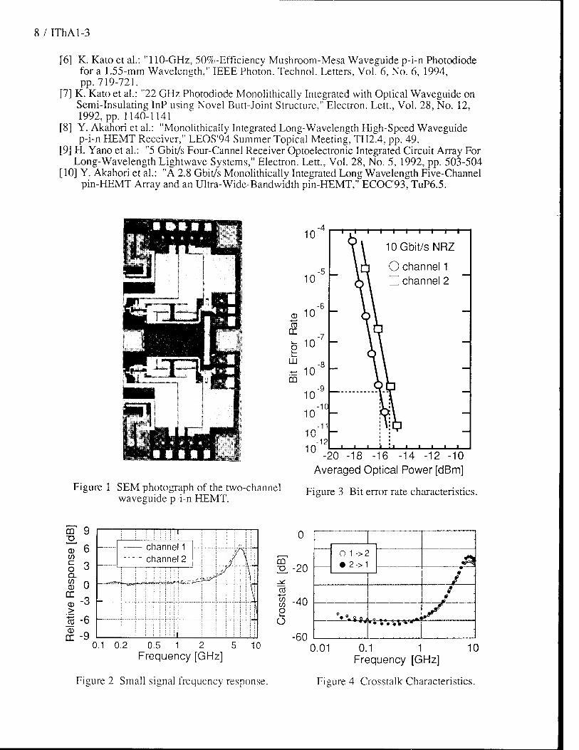
Figure 1 SEM photograph of the two-channel waveguide p-i-n HEMT.
10
10
CD 03
10 -6
10 -7
UJ
- 10 m
10'
10 -1C
10
10
-11
-12
T—1 1 1 1
10 Gbit/s NRZ
O channel 1 D channel 2
-1—1 I ill I I I I L. 20 -18 -16 -14 -12 -10
Averaged Optical Power [dBm]
Figure 3 Bit error rate characteristics.
0.1 0.2 0.5 1 2 5 Frequency [GHz]
0Ü 2.-20
CO
w co o
- Ü
-40
-60
• O 1 ->2 • 2->1 «^
• I t '
a I
°« °t2ej / ■
0.01 0.1 1 Frequency [GHz]
10
Figure 2 Small signal frequency response. Figure 4 Crosstalk Characteristics.

IThA2-l / 9
A Waveguide InAlAs / InGaAs Superlattice Avalanche Photodiode with a 120-GHz Gain-Bandwidth Product
M. Shishikura, H. Nakamura, S. Hanatani, S. Tanaka, H. Sano, and S. Tsuji
Central Research Laboratory, HITACHI, Ltd. 1-280, Higashi-koigakubo, Kokubunji-shi, Tokyo 185, JAPAN
Tel: +81-423-23-1111 Fax: +81-423-27-7673
1. INTRODUCTION An avalanche photodiode (APD) with both an ultra-wide bandwidth and a high
quantum efficiency is attractive for use in compact, highly-sensitive photoreceivers in optical communication systems at a wavelength of 1.55 \im. APDs with superlattice (SL) avalanche multiplication structures [1, 2, 3] are advantageous for obtaining a large gain-bandwidth (GB) product because their SL multiplication layers have high ionization-rate ratios. However, it is difficult to obtain a wide bandwidth above 20 GHz, while keeping a high quantum efficiency in conventional top- or back-illuminated SL-APDs [1] because there is a tradeoff between the quantum efficiency and the 3dB bandwidth which is limited by the carrier-transit time. On the other hand, in a photodiode with a waveguide (WG) structure, the quantum efficiency is independent of the bandwidth because the incident light and photogenerated carriers travel in different directions [4]. K. Kato et al. [5] reported a wide bandwidth of 110 GHz and a high quantum efficiency of 50% for a waveguide p-i-n photodiode (PIN-PD). This clarified the advantage of introducing a waveguide structure into SL-APDs for ultra-high-speed operation.
We previously proposed an edge-coupled SL-APD with a waveguide structure in which stable avalanche multiplication characteristics were observed with no edge breakdown at a wavelength of 1.55 urn [6]. However, deterioration of the frequency response due to distribution of the photogenerated carriers in the absorption layer, and degradation of the GB product due to electron-hole mixed injection into the SL multiplication layer [7] are viable risks in WG-SL-APDs, whereas they are not in conventional SL-APDs. Therefore, it is necessary to experimentally confirm that a wide bandwidth and a large GB product can be obtained simultaneously in the WG-SL- APDs.
In this paper, a WG-SL-APD fabricated with an InAlAs/InGaAs SL multiplication layer is analyzed. A maximum 3dB bandwidth of 11 GHz and a large GB product of 120 GHz, comparable to that of the conventional back-illuminated SL-APD, are demonstrated at a wavelength of 1.55 [im.
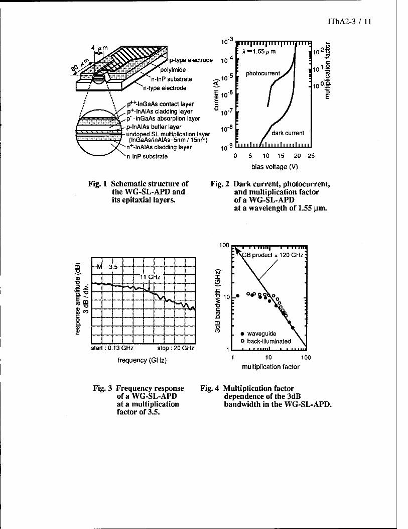
2. DEVICE STRUCTURE The schematic structure of the WG-SL-APD fabricated for this study is shown in
Figure 1. The epitaxial layers were grown by molecular beam epitaxy (MBE) on an InP substrate. These layers were made up of an n+-InAlAs cladding layer, a 9-period undoped InAlAs/InGaAs SL multiplication layer, a p-InAlAs buffer layer, a p"-InGaAs absorption layer, a p+-InAlAs cladding layer, and a p++-InGaAs contact layer. The thickness of the InGaAs well and InAlAs barrier in the SL multiplication layer was 5
10 / IThA2-2
nm and 15 nm, respectively, giving a GB product of 130 GHz in the back-illuminated type[3]. The InGaAs absorption layer was only 0.4-fim thick, corresponding to a bandwidth of 50 GHz as limited by the carrier-transit time.
The waveguide was covered with polyimide for passivation. Ti /Au and AuGeNi were evaporated for the p-type and n-type electrodes, respectively. The waveguide was 4 |im-wide and 80-fim long without AR coating.
3. EXPERIMENTAL RESULTS Figure 2 shows the dark current, photocurrent and multiplication factor for the
fabricated WG-SL-APD at a wavelength of 1.55 Jim. Stable avalanche multiplication is evident with no edge breakdown, and the maximum multiplication factor is more than 50. The dark current is about 0.3 jxA for a multiplication factor of 10. This means that the received power penalty due to the dark current is negligible at bit rates higher than 10 Gbit/s.
Figure 3 shows the frequency response of the WG-SL-APD for a multiplication factor of 3.5: the maximum 3dB bandwidth here is 11 GHz. The WG-SL-APD chip has a total capacitance of 0.25 pF. The bonding-pad and waveguide-active-layer capacitances are 0.20 pF and 0.05 pF, respectively. The maximum 3dB bandwidth corresponds with that limited by the CR-time constant, indicating that there was little frequency-response deterioration due to distribution of the photogenerated carriers in the absorption layer. It is possible to raise the maximum 3dB bandwidth to 30 GHz by reducing the bonding-pad capacitance through flip-chip bonding.
Figure 4 shows the 3dB-bandwidth dependence on the avalanche multiplication factor at a wavelength of 1.55 (im. Here, the closed and open circles denote the characteristics of the waveguide and the conventional back-illuminated SL-APD, respectively. The 3dB bandwidths for multiplication factors above 10 are limited by the avalanche build-up time. The GB product for this device is 120 GHz, which is comparable to that of a conventional back-illuminated SL-APD with the same multiplication structure. These results indicate that there was no degradation in the GB product due to electron-hole mixed injection into the SL multiplication layer. Therefore, it is possible to obtain both a wide bandwidth and a large GB product in the WG-SL-APD, as needed for ultra-high-speed optical communication systems.
4. SUMMARY A maximum 3dB bandwidth of 11 GHz and a large GB product of 120 GHz, which
is comparable to that of a back-illuminated SL-APD, have been demonstrated for the first time in a WG-SL-APD. It has been experimentally confirmed that there is little frequency-response deterioration due to distribution of the photogenerated carriers in the absorption layer and no GB-product degradation due to electron-hole mixed injection into the SL multiplication layer.
REFERENCES [1] T. Kagawa et al., IEEE J. Quantum Electron. Vol. 29, pp. 1387-1392 (1993). [2] I. Watanabe et al., IEEE Photonics Technol. Lett. Vol. 5, pp. 675-677 (1993). [3] S. Hanatani et al., Tech. Dig. of OFC / IOOC '93 ThG3, pp. 187 (1993). [4] J. E. Bowers et al., IEEE J. Lightwave Technol. Vol. LT-5, pp. 1339-1350 (1987). [5] K. Kato et al., IEEE Photonics Technol. Lett. Vol. 6, pp. 719-721 (1994). [6] M. Shishikura et al., Tech. Dig. of OEC '94 13D1-3, pp. 68-69 (1994). [7] S. Hanatani et al., Microwave and Optical Technol. Lett. Vol. 7, pp. 103-107 (1994).
IThA2-3 / 11
4 //m
p-type electrode
polyimide
n-lnP substrate
n-type electrode
. p+^lnGaAs contact layer „ p+-lnAIAs cladding layer
=9*^-P" -InGaAs absorption layer "^*T-p-lnAIAs buffer layer
undoped SL multiplication layer (lnGaAs/lnAIAs=5nm /15nm)
• n+-lnAIAs cladding layer
'n-lnP substrate
10"
10"
^10"° <
Iio-6
10"
IIIIIIIIIIIIIIIIIIIJIIII A=1.55/im
photocurrent
10"
10"
M02|
3io°I E
dark current
1111111 /■ 11111111111111
5 10 15 20
bias voltage (V)
25
Fig. 1 Schematic structure of the WG-SL-APD and its epitaxial layers.
Fig. 2 Dark current, photocurrent, and multiplication factor of a WG-SL-APD at a wavelength of 1.55 |j.m.
100
start: 0.13 GHz stop : 20 GHz
frequency (GHz)
N X C5
? 10 '5 c CO n
CO ■o CO
1
I I I mill 1 I IIIIIJ SB product = 120 GHz;
• waveguide o back-illuminated
■■■■'
1 10 100
multiplication factor
Fig. 3 Frequency response of a WG-SL-APD at a multiplication factor of 3.5.
Fig. 4 Multiplication factor dependence of the 3dB bandwidth in the WG-SL-APD.

12 / IThA3-l
Integrated Optical (de-) Multiplexers/Filters on InP
Bart H. Verbeek Philips Optoelectronics Centre
5656 AA Eindhoven, The Netherlands
and
Technical University of Delft Laboratory of Telecommunication Technology
An overview of recent progress of InP based multiwavelength devices (de-multiplexer, filter) will be presented. The performance of grating- and phased array (PHASAR) based devices is compared. In particular key parameters like number of channels, channel spacing, losses, crosstalk and polarization (in-) dependence are addressed.
IThA4-l / 13
High speed pin-HEMT receiver OEICs
Yuji Akatsu, Yuji Akahori*, and Yoshio Itaya
NTT Optoelectronics Laboratories
3-1 Morinosato Wakamiya, Atsugi, Kanagawa, 243-01 Japan
NTT Opto-electronics Laboratories
Tokai, Ibaraki, 319-11 Japan
Several long-wavelength monolithically integrated photoreceivers have recently been
developed [1-8] for high-speed optical transmission systems and optical interconnection
systems, because of a small amount of parasitic capacitance and inductance, small receiver size
and packaging simplicity. These receiver OEICs combined photodetectors, such as surface-
illuminated pin-photodiodes and MSM photodiodes, and high speed transistors, such as
heterojunction bipolar transistors (HBTs) and high electron mobility transistors (HEMTs).
That is, these OEICs consisted of combinations of pin-HBTs, MSM-HEMTs or pin-HEMTs.
The OEICs have excellent features as mentioned above, however, in order to realize the full
range of OEIC capabilities, opto-electronic device integration technologies must be advanced to
assure uniformity of device characteristics on a wafer, surface flatness, and process simplicity
without deteriorating electronic and optical performance each other.
The pin-HEMT photoreceiver demonstrated here employs an InGaAs pin-photodiode
(pin-PD) and InGaAs HEMTs. We adopted a planar doping technique and an ion implantation
in order to enhance the uniformity of the HEMTs and the pin-PD and we used one-step growth
for process simplicity. This combination of techniques enabled 15-Gbit/s operation, and the
use of a waveguide-type pin-PD and HEMTs with shorter gate length is expected to result in
even faster operation.
Figure 1 is a cross-sectional view of the pin-HEMT photoreceiver [9]. This structure
was grown using one-step growth with low-pressure MOVPE. The InGaAs HEMTs are the
bottom eight layers and the InGaAs pin-PD is the top three layers. The diameter of the pin-PD was 20 (im. The HEMTs had a gate length of 1 |0.m, an extrinsic transconductance of
630 mS/mm, and a current gain cut-off frequency of 25 GHz. The pin-HEMT circuit
employed a transimpedance amplifier and the 3-dB bandwidth was 7.4 GHz.
The high-speed operation at 10 Gbit/s was evaluated using an erbium-doped fiber
amplifier (EDFA) ahead of the pin-HEMT. Figure 2 shows the bit error rate characteristics of
the 10-Gbit/s lightwave signals at a wavelength of 1.55 |J.m transmitted 0 and 150 km. The
inset shows the eye patterns at the output of the pin-HEMT. The receiver sensitivity at a bit-
error rate of 1 x 10"" is -30.6 dBm for both transmission lengths. No degradation was
observed after transiting. This result verifies the feasibility of pin-HEMT photoreceivers for
high-speed transmission systems.
14 / IThA4-2
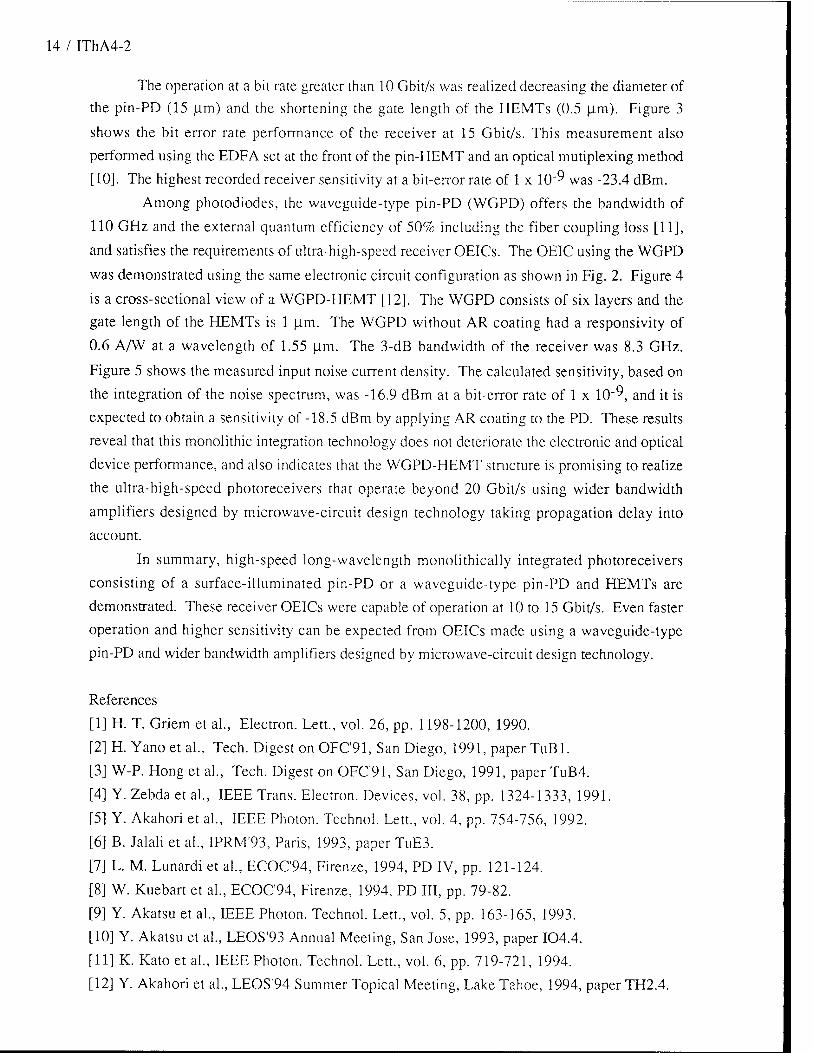
The operation at a bit rate greater than 10 Gbit/s was realized decreasing the diameter of the pin-PD (15 pm) and the shortening the gate length of the HEMTs (0.5 |im). Figure 3
shows the bit error rate performance of the receiver at 15 Gbit/s. This measurement also
performed using the EDFA set at the front of the pin-HEMT and an optical mutiplexing method
[10]. The highest recorded receiver sensitivity at a bit-error rate of 1 x 10~9 was -23.4 dBm.
Among photodiodes, the waveguide-type pin-PD (WGPD) offers the bandwidth of
110 GHz and the external quantum efficiency of 50% including the fiber coupling loss [11],
and satisfies the requirements of ultra-high-speed receiver OElCs. The OEIC using the WGPD
was demonstrated using the same electronic circuit configuration as shown in Fig. 2. Figure 4
is a cross-sectional view of a WGPD-HEMT [12]. The WGPD consists of six layers and the
gate length of the HEMTs is 1 (im. The WGPD without AR coating had a responsivity of
0.6 AAV at a wavelength of 1.55 p.m. The 3-dB bandwidth of the receiver was 8.3 GHz.
Figure 5 shows the measured input noise current density. The calculated sensitivity, based on
the integration of the noise spectrum, was -16.9 dBm at a bit-error rate of 1 x 10~9, and it is
expected to obtain a sensitivity of-18.5 dBm by applying AR coating to the PD. These results
reveal that this monolithic integration technology does not deteriorate the electronic and optical
device performance, and also indicates that the WGPD-HEMT structure is promising to realize
the ultra-high-speed photoreceivers that operate beyond 20 Gbit/s using wider bandwidth
amplifiers designed by microwave-circuit design technology taking propagation delay into
account.
In summary, high-speed long-wavelength monolithically integrated photoreceivers
consisting of a surface-illuminated pin-PD or a waveguide-type pin-PD and HEMTs are
demonstrated. These receiver OEICs were capable of operation at 10 to 15 Gbit/s. Even faster
operation and higher sensitivity can be expected from OEICs made using a waveguide-type
pin-PD and wider bandwidth amplifiers designed by microwave-circuit design technology.
References
[I] H. T. Griem et al., Electron. Lett., vol. 26, pp. 1198-1200, 1990.
[2] H. Yano et al., Tech. Digest on OFC'91, San Diego, 1991, paper TuBl.
[3] W-P. Hong et al., Tech. Digest on OFC'91, San Diego, 1991, paper TuB4.
[4] Y. Zebda et al., IEEE Trans. Electron. Devices, vol. 38, pp. 1324-1333, 1991.
[5] Y. Akahori et al., IEEE Photon. Technol. Lett., vol. 4, pp. 754-756, 1992.
[6] B. Jalali et al., IPRM'93, Paris, 1993, paper TuE3.
[7] L. M. Lunardi et al, ECOC94, Firenze, 1994, PD IV, pp. 121-124.
[8] W. Kuebart et al., ECOC94, Firenze, 1994, PD III, pp. 79-82.
[9] Y. Akatsu et al., IEEE Photon. Technol. Lett., vol. 5, pp. 163-165, 1993.
[10] Y. Akatsu et al, LEOS'93 Annual Meeting, San Jose, 1993, paper I04.4.
[II] K. Kato et al., IEEE Photon. Technol. Lett., vol. 6, pp. 719-721, 1994.
[12] Y. Akahori et al, LEOS'94 Summer Topical Meeting, Lake Tahoe, 1994, paper TH2.4.

IThA4-3 / 15
HEMT pin-PD insulating layer incident light passivation film
.JT. / p electrode
i- InP , i - InGaAs
S. I. InP substrate
Fig. 1. Cross-sectional view of monolithically integrated pin-HEMT photoreceiver composed of a InGaAs pin-PD and InGaAs HEMTs.
CD
CO OC
O \- uu
m
WGPD p electrode
p+- InGaAs p+- InP
HEMT
n - InAIAs p+-lnGaAsP + . _ .
n - InGaAs i - InGaAs
InGaAsP drain n+- InP
S. I. InP substrate n electrode
Fig. 4. Cross-sectional view of WGPD-HEMT composed of a waveguide pin-PD and HEMTs.
ö N X
<: Q.
CO
a Q •♦—> c CD i— ^_
Ü CD CO
3 a. c
—1—1—1—1— T—i—i—i—i—i—i—r— 1—
! I ! i
_
11 1 -5 ms*'*:'*******»
10 "■■+" t " j 1 ' 1~:U "■"■* f "11 i r
10Gbit/sNRZ -
-7 1U k 0 0 km
V • 150 km
-9 10 V -
-11 10
1 1 1 1 1 1 1 1 1 1 1 1 1
-35 -30 -25 Average Received Power (dBm)
Fig.' 2. Bit error rate performance of 10-Gbit/s signals transmitted 0 and 150 km using an EDFA ahead of the pin-HEMT. The inset shows the eye pattern at 10Gbit/s(25ps/div.).
0.1 1 Frequency (GHz)
Fig. 5. Input noise current density of the WGPD-HEMT.
-30 -25 -20 Average Received Power (dBm)
Fig. 3. Bit error rate performance using the EDFA ahead of the pin-HEMT. After detection, the 15 Gbit/s signal was elecrtically demultiplexed to 7.5 Gbit/s, and the bit error rate of each signal was measured. The inset shows the eye pattern at 15 Gbit/s (20 ps/div.).

16 / NOTES

Thursday, February 23, 1995
Beam Propagation Techniques
IThB 10:30 am-11:45 am Salon 4
G. Ronald Hadley, Presider Sandia National Laboratories
18 / IThBl-1
Improved Field Propagation Techniques
David Yevick Department of Electrical Engineering, Queen's University Kingston, Ontario K7L 3N6, Canada,
613-545-6731, FAX:613-545-6774, yevick@qucdnee
The following text summarizes research co-authored during 1994 with John Yu (RN'R), Björn Hermans-
son (Telia AB), David Thomson (DREP), Yosef Yayon (Technion) and Moses Glasner (Pennsylvania State
University) on various aspects of electric field propagation methods. Several numerical results are also
presented.
Transparent Boundary Conditions: Despite the popularity of transparent, boundary conditionsfl] spurious
reflections at can still be problematic if the electric field at the boundary possesses a large angular spread.
After a careful investigation we have however concluded that the reflection coefficient for an absorber which
is somewhat wider than the maximum transverse wavelength of the dominant electric field components is
often substantially less than that associated with the standard transparent boundary condition.[2] Further,
combining absorbing and transparent boundary conditions in general further reduces spurious reflections
since large-angle field components are attenuated before the field impinges on the boundary. To illustrate,
we compare the propagating antisymmetric field in a step-index waveguide with An = 0.014 calculated with
a pure transparent boundary condition and a hybrid absorbing/transparent condition in Figs.(l) and (2),
respectively, for a transverse window length of 8pm, A0 = 1.56pm and 7idad = 3.166pm.
Split-Operator Procedures: Although wide-angle procedures based on the approximation
kanoVl + H = ^Jkln2 + V'{ « ka(n - n0) + y/k'^n~ + V\ (1)
are highly effective for small refractive index variations, phase errors among different field components are
at times significant. We have therefore introduced a simple hybrid procedure which retains only the first
non-trivial Taylor series corrections to Eq.(l) and can accordingly be implemented with tridiagonal matrix
solvers. This method generates accurate phase shifts and is far less sensitive to the choice of reference wave
vector than the standard procedure as demonstrated by the comparison in Fig.(3) between the hybrid method
(Q2'), the Fresnel approximation (Q0), the wide-angle procedure of Eq.(l) (Ql') and the exact acoustic loss
(SAFARI) at 80km as a function of reference sound speed for the leaky surface duct test case posed by Porter
and Jensen with the source and receiver located inside the duct.[3, 4]
Lanczos Technique: As is well-known, Lanczos propagation methods for the full Helmholtz propagator ex-
hibit slow convergence in several representative contexts.[4, 5] We demonstrate first that such difficulties
can be largely surmounted if the Lanczos algorithm is instead applied exclusively to the higher-order cor-
rections to Eq.(l).[4] Next, we examine for a near point-source initial excitation both standard and Lanczos
propagation techniques based on Taylor, Pade and Chebyszev-Pade expansions of either \/T+~H — 1 or the
corresponding exponential propagation operators. We find that if the exponential of a term proportional
to the imaginary part of the right-hand side of Eq.(l) is applied after each propagation step in order to
remove evanescent modes, the precision of wide-angle predictions at short propagation lengths as well as
the convergence rate of Lanczos algorithms can be greatly increased.[6] For example, for a near point-source
excitation in a homogeneous medium the relative accuracy of the calculated electric field magnitude at a
certain grid point, which is given as a function of longitudinal distance by the third highest curve in Fig.(4)
for the [3,3] wide-angle Pade operator, improves to the lowest, curve in the figure if the exponential of the
imaginary part of Eq.(l) is applied. The method is however most precise for homogeneous media.
IThBl-2 / 19
Vector Beam Propagation: Since finite-difference propagation techniques for the full vector wave equation
lead to asymmetric, non-unitary propagation operators, for dense transverse computational grids and large
refractive index changes the electric field will grow rapidly upon propagation for any choice of longitudinal
step size. The asymptotic field distribution is then given by the modal eigenfunction with the largest
value for the imaginary part of the propagation constant assuming a forward-travelling field with e~lwt
time dependence. The divergence can presumably be suppressed under certain conditions by absorbing or
transparent boundary conditions.
A previously employed stabilizing procedure is to apply a compensating direct, non-unitary propaga-
tor over a small interval of each propagation step. Such a technique however can significantly attenuate
non-evanescent field components. Another possible approach is to multiply by the exponential of a term
proportional to the imaginary part of Eq.(l) after each propagation step; however for discontinuous media
the high spatial frequencies created by the refractive index derivatives in the vector wave equation are spuri-
ously attenuated.[7] We are therefore led to consider procedures based on modified Pade expansions for the
exponent of the Helmholtz propagation operator or for the propagation operator itself.[7, 8] In the former
case, the coefficients of the modified [m,m] approximant can for example be determined by simultaneously
imposing both the conditions that at H = 0 the first m - 1 derivatives of the approximant agree with the
corresponding in - 1 derivatives of the square-root operator and the requirement that the Pade expression
yields a certain positive imaginary value, c, at a value H = -a. The constants a and e are generally set
empirically although some indication of their value is given by Gerschgorin's theorem or by the rate of di-
vergence of the electric field in the standard vector propagation method. In this connection, the number of
conditions applied to the non-evanescent part of the spectrum can be decreased tom — p while the Pade and
square-root operators can be set equal at p points in the complex plane chosen to reflect the upper bounds
for the imaginary eigenvalues. In Fig.(5) we accordingly display the L2 field norm in the standard vector
procedure with zero boundary conditions for a rectangular semiconductor waveguide in vacuum excited by
pointlike sources inside and outside the waveguide. The divergence is fully removed by the third-order Pade
approximant of [8], cf. Fig (6).
[1] G. Hadley, "Transparent boundary condition for the beam propagation method," IEEE J. Quant. Elec-
tron., vol. 28, pp. 363-370, 1992.
[2] D. Yevick, J. Yu, and Y. Yayon, "Optimal absorbing boundary conditions,". To be published in J. Opt.
Soc. Am. A.
[3] M. Porter and F. Jensen, "Anomalous parabolic equation results for propagation in leaky surface ducts,"
J. Acoust. Soc. Am., vol. 94, pp. 1510-1516, 1993.
[4] D. Yevick and D. Thomson, "Split-step/finite difference and split-step/Lanczos algorithms for solving
higher-order parabolic equations," J. Acoust. Soc. Am., vol. 96, pp. 396-405, 1994.
[5] B. Hermansson, D. Yevick, W. Bardyszewski, and M. Glasner, "A comparison of Lanczos electric field
propagation methods," IEEE J. Light. Technol, vol. 10, pp. 772-776, 1992.
[6] D. Yevick and B. Hermansson, "Convergence properties of wide-angle techniques,". To be published in
Photon. Technol. Lett.
[7] D. Yevick, J. Yu, and M. Glasner, "Stability issues in vector electric field propagation,". Submitted to
Photon. Technol. Lett.
[8] M. Collins, "Higher-order Pade approximations for accurate and stable elastic parabolic equations with
application to interface wave propagation," ./. Acoust. Soc. Am., vol. 89, pp. 1050-1057, 1991.

20 / IThBl-3
Propagation Di Propagation Distance
Figure 1: Transparent Boundary Condition Figure 2: Transparent Boundary Condition with Absorber
1480 1490 1500 1510 Reference Sound Sp©©d
1520 1530 10 12 Propagation Distance in Microns
Figure 3: Improved Split-Step Algorithm Figure 4: Comparison of Pade and Lanczos Methods
0 100 200 300 400 Longitudinal Distance in Microns
0.7, 0 100 200 300 400
Longitudinal Distance in Microns
Figure 5: Standard Vector Propagation Procedure Figure 6: Modified Vector Propagation Procedure

IThB2-l / 21
A wide-angle beam propagation method using the generalized Douglas scheme for variable coefficients
Junji YAMAUCHI, Jun SHIBAYAMA, Hisamatsu NAKANO
College of Engineering, Hosei University 3-7-2, Kajino-cho, Koganei, Tokyo 184, Japan
Tel: 423-87-6190, Fax: 423-87-6048
1. INTRODUCTION The accuracy of the conventional finite-difference beam propagation
method (FD-BPM) [1] is degraded in the analysis of wide-angle propagation because the paraxial approximation is employed. To avoid this degradation, Hadley [2] proposed the technique using Pade approximant operators for the FD-BPM based on the Crank-Nicholson (CN) scheme.
The CN scheme has the truncation error of 0(Ax)2 in the transverse direction. To reduce the truncation error, Yevick et al. [3] applied the Douglas scheme to the paraxial wave equation using the split-step procedure. On the other hand, Sun and Yip [4] formulated the modified FD- BPM based on the Douglas scheme without splitting the phase term. Their formulation has an advantage that the numerical result is not a sensitive function of a propagation step length. However, they do not take into account variable coefficients in the phase term, resulting in slight improvement in the accuracy. Recently, we have presented the modified FD- BPM based on the generalized Douglas (GD) scheme for variable coefficients, in which the truncation error of 0(Ax)4 is assured with substantial improvement in the accuracy [5].
The purpose of this paper is to formulate the FD-BPM based on the GD scheme with the (1,1) Pade approximant operator [2]. This is the first application of the GD scheme to a wide-angle FD-BPM. The present scheme achieves the truncation error of O(Ax)4, maintaining a tridiagonal system of linear equations. The numerical results show that the present scheme offers further improvement in the analysis of wide-angle beam propagation.
2. DISCUSSION When the (1,1) Pade approximant operator is employed [2], the scalar
Helmholtz equation in a two-dimensional problem reduces to
3E -Joir/(i+i-2) E , (i) 9z J2k ' VJ- 4k2
where P=32/3x2+k02[n(x,z)2-n0
2] and k=k0n0 in which k<> is the free space wavenumber, n(x,z) is the index profile of the waveguide, and n0 is the reference refractive index to be appropriately chosen. For the difference equations, the simplifying symbol of E(iAx,mAz)=ET is used.
We apply the GD scheme to Eq.(l) [5]. Then, the following difference equation is derived:
Ax2 " 12 (<T 3z ,A*1+ 6 l(T 3z ,1+ 12 (<T 3z
1y(vE)i.1 --^(vEh - jj(vE)L-^ 0(Ax)4 , (2)
22 / IThB2-2
where (52E)i=E1.1-2Ei+Ei-1, (7=2jk(l+P/4k2) and v=k02[n(x,z)2-n0
2]. It should be noted that the second derivatives with respect to the transverse direction appear in (cr3E/3z)1±I. The centered difference formula is usually used for a second derivative. However, this leads to a pentadiagonal matrix with a computational penalty. In order to maintain a tridiagonal matrix, we employ the forward and backward difference formulas for the second derivatives in (odE/Zz),.-! and (cr9E/3z) x^, respectively.
After some manipulations, we obtain the following finite-difference equation with centered z difference:
where
rm - J-. 1+ajkAz , _i_ i _, 5 1+a.ikAz , 2 5 m, W±1 " 12 4k2 ( Ax2 + 12 Vl±l) ' Ci = 6 " 4k2 ( Äx"2 " TVi) '
in which a = -1 : m +1 : m+1 .
Eq.(3) can be solved by efficient techniques such as the Thomas algorithm. It follows that the computation time of the present scheme is almost identical with the FD-BPM based on the CN scheme. The transparent boundary condition [6] can easily be imposed.
We investigate the propagation error of the fundamental mode in a tilted step-index slab waveguide illustrated in Fig.l. The core width is 2D=7.546ym and a wavelength of A.=lnm is used. The refractive indices of the core and cladding are NCo=1.002 and NCL=1.000, respectively. The reference refractive index is chosen to be that in the cladding.
Fig.2 shows the coupling efficiency evaluated at a propagation distance of 200/im as a function of tilt angle 9. The propagation step length is Az=0.5/jm, the transverse sampling width is Ax=D/(14cos9)=D'/14 and the number of the transverse sampling points is 800.
We first discuss the paraxial case which corresponds to the (1,0) Pade approximation shown in Fig.2 (a). The phase shift of the field in the transverse direction becomes large as the tilt angle is increased. Therefore, the result obtained from the GD scheme attains higher accuracy than that from the CN scheme, particularly when the tilt angle is large. Fig.2 (b) shows the case where the (1,1) Pade operator is used. A comparison between Figs. 2 (a) and (b) shows that the GD scheme with the (1,1) Pade operator can further improve the accuracy.
An example of the propagating field for 0=20° is shown in Fig. 3. The (1,1) Pade operator is used and the computation parameters are the same as those in Fig.2. It is seen that the field observed for the GD scheme propagates in the tilted waveguide without being deformed. But the field observed for the CN scheme shifts toward the -x direction.
3. CONCLUSIONS We have shown that the accuracy of a wide-angle beam propagation method
with the (1,1) Pade approximant operator can be improved by using the generalized Douglas scheme. The truncation error is reduced to 0(Ax)4 in the transverse direction maintaining a tridiagonal system of linear equations. We demonstrate its effectiveness in the analysis of a tilted slab waveguide and show an example of the propagating field.
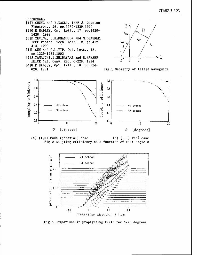
IThB2-3 / 23
REFERENCES [1]Y.CHUNG and N.DAGLI, IEEE J. Quantum
Electron., 26, pp.1335-1339,1990 [2]G.R.HADLEY, Opt. Lett., 17, pp.1426-
1428, 1992 [3]D.YEVICK, B.HERMANSSON and M.GLASNER,
IEEE Photon. Tech. Lett., 2, pp.412- 414, 1990
[4]L.SUN and G.L.YIP, Opt. Lett., 18, pp.1229-1231,1993
[5]J.YAMAUCHI,J.SHIBAYAMA and H.NAKANO, IEICE Nat. Conv. Rec. C-228, 1994
[6]G.R.HADLEY, Opt. Lett., 16, pp.624- 626, 1991
-D' 0 D
Fig.l Geometry of tilted waveguide
o a
O
00 c 'H. o ü
1.0
0.8
0.6
0.4
0.2
0.0
GD scheme
CN scheme
0 lfl
8 [degrees]
ü c
a)
bo a
"p. 3 O Ü
20
1.0
0.8
0.6
0.4
0.2
0.0
GD scheme
CN scheme
0 10
6 [degrees]
20
(a) (1,0) Pade (paraxial) case (b) (1,1) Pade case Fig.2 Coupling efficiency as a function of tilt angle 0
200-
=1 i p
tsi
o c CO
+-> w -3
.2 10° +J cO bO CO O. O l-i
GD scheme
CN scheme
-40 0 40 80 transverse direction X [/zm]
Fig.3 Comparison in propagating field for 0=20 degrees

24 / IThB3-l
New vector-BPM in cylindrical coordinates based on
the Method of Lines
R. Pregla and E. Ahlers Allgemeine und Theoretische Elektrotechnik
FernUniversität, 58084 Hagen, Germany Telephone: +49 2371 566 256
Fax: +49 2371 51898
Most Beam Propagation Methods (BPM) base on the cartesian coordinate system. In this paper a new vector-BPM based on the Method of Lines in cylindrical coordinates is presented.
The characteristics of the method are
• the full wave equations are used • large refrective index steps in all directions are allowed • reflections are taken into account and can be calculated • absorbing boundary contitions are used
The method starts with the general vectorial wave equation from [1] (r and z are normalized to the free space wave number k0 : f = k0r, I — k0z)
v2ne-£-1(ve)v-ne + £rfie = o
In the general case the permittivity is a function of all coordinates: er = £r(f, <p,t).
The field components are derived from the vector potential ne by the equations
TJOH = jV x Ee E = er-JV x V x fie
770 is the free space wave impedance. In cylindrical coordinates IIe is written as ne = {nr, 11^, 11^}
With these components we get three coupled wave equations:
Ö 1 0/-¥T £r^r I — T=(rnr or \£rr dr
1 d2nr <92nr „ 0 f2 dp2
dz d 1 on. dr \err dtp ) r dtp \r dr v'
r dr
£,0/1 d , „
r a<p \err or
err dp
d /idnr
0
ö2n. L^A + ^ + ^ + .4
df \r dtp = 0
a2n, dfdJ
+
.xön, i<92n2
r dtpdz +
1 d ( an r dr \ dr
+ 1 d2n f2 dtp2 dz
+ erTl2+
^l^l^ 9 fi d , „ dz \r of
+ e, uu^)-m>^° The field components are transformed to
~ldll2 duu VoHr = j
VoHtp = J
VoHz = j
r dtp dz
dlir dU
dJ d't
, F -1 d
r dtp
erE, - -
1 d 1 cm, r dr ^ r dtp
dn
d_ dz
önr du* dz
190r
f dtp £rEz =
1 d r±jz — _
r dr
=>■■ r dtp
dz
'v dz .
_<9n
d_ dr
8r
id 1 anr -^r('-n¥,)- -—— r of r dtp
dr
ld_
f dtp
i<9nz diLv
f dtp dz

IThB3-2 / 25
Now we choose the special case
n, = o «V = er(<p,r)
That leads to the wave equations
4(^H+? 1 O^IIr #%. 8<p2 + &Z2 n d ( 1 gIM l d (l d (ra ^ =o r rdr \err dy? / r d<p \r df /
° f1 d ,-rr s\ , £r 0 ( 1 Ö(rII^)\ Ö3II„ £r Ö / 1 Ö \ 0 /l 0IIr \
with the coresponding field components
m Hr -3- dz erEr fd(p
trEtp ~ "OF
r dr f dtp
n a ,_„ , ianr rar r cV ÖT2 *
loHz = j i ö iönr r or r o<p r dr \ dz / r öy>dz v
With the ^-dependencies for circular waveguides
nr~cosmy> nv,~sinmy> and er = £r(r)
the derivation with respect to <p in the above wave equations can be eleminated and we have only derivations with respect to r and z~.
As usual in the Method of Lines we discretize only as long as necessary. With the above depen- dencies to ip it is sufficient to discretize only the r-direction. Without these dependencies we must discretize the r- and y-direction. In z-direction the wave equations are solved analyticaly. After discretizing IIr(=>- r/>) and II¥,(=>- <f>) the wave equations are
dz2 4> Q = o
with
Q =
T-l h eeD* r^c^Dre-Ce+m2^2 h {ceDi mr^e^1 -m rJ2r>Vfc)
■5—1 h (-D m r'1 + m r, 2Dre) h 2D r-1Dtrh-eh+m2rT2
D = difference operator representing the first derivative
h = normalized discretization length in r-direction
re = diagonal matrix of the normalized radii at the positions of V>
r& = diagonal matrix of the normalized radii at the positions of <f>
After diagonalization of Q
we get the analytical solution
T QT = r
t 4>
= e +<?' <t>-
= T
where subscript + means propagation in positive z-direction and subscript — propagation in ne- gative z-direction.
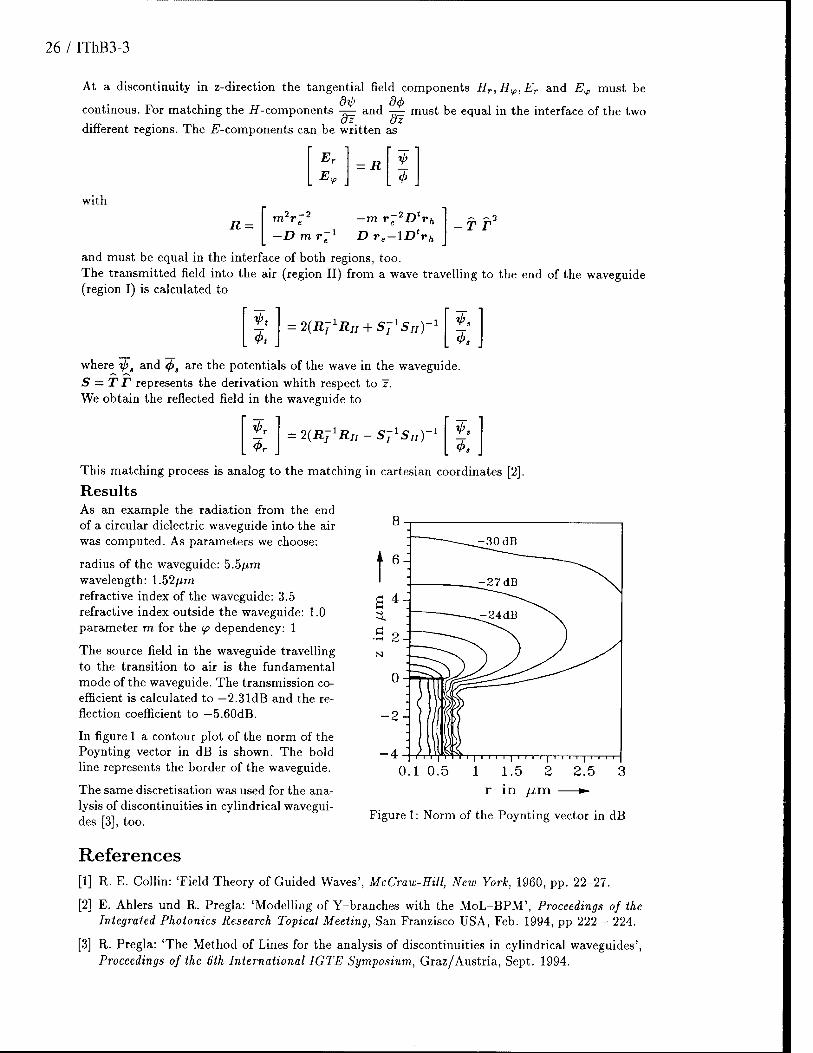
26 / IThB3-3
At a discontinuity in z-direction the tangential field components Hr,Hv,Er and Ev must be
continous. For matching the //-components -?— and -—; must be equal in the interface of the two . az oz
different regions. The E'-components can be written as
E
E. <p
= R t 4>
with
R = -T r n2r-2 -m r^D*^ -Dmr-1 Dre-lD*rh
and must be equal in the interface of both regions, too. The transmitted field into the air (region II) from a wave travelling to the end of the waveguide (region I) is calculated to
<t>t 2(Rj Ru + Sj Sa)
4>s
where ips and <j>s are the potentials of the wave in the waveguide. S — T r represents the derivation whith respect to z. We obtain the reflected field in the waveguide to
<f>r 2(RJ1RII-SJ1SII)-
1
4>s
8 30 dB
This matching process is analog to the matching in cartesian coordinates [2].
Results As an example the radiation from the end of a circular dielectric waveguide into the air was computed. As parameters we choose:
radius of the waveguide: 5.5pm wavelength: 1.52/im refractive index of the waveguide: 3.5 refractive index outside the waveguide: 1.0 parameter m for the (p dependency: 1
The source field in the waveguide travelling to the transition to air is the fundamental mode of the waveguide. The transmission co- efficient is calculated to —2.31dB and the re- flection coefficient to —5.60dB.
In figure 1 a contour plot of the norm of the Poynting vector in dB is shown. The bold line represents the border of the waveguide.
The same discretisation was used for the ana- lysis of discontinuities in cylindrical wavegui- des [3], too.
0.1 0.5
Figure 1: Norm of the Poynting vector in dB
References [1] R. E. Collin: 'Field Theory of Guided Waves', McCraw-HUl, New York, 1960, pp. 22-27.
[2] E. Ahlers und R. Pregla: 'Modelling of Y-branches with the MoL-BPM', Proceedings of the Integrated Photonics Research Topical Meeting, San Franzisco USA, Feb. 1994, pp 222 - 224.
[3] R. Pregla: 'The Method of Lines for the analysis of discontinuities in cylindrical waveguides', Proceedings of the 6th International IGTE Symposium, Graz/Austria, Sept. 1994.

IThB4-l / 27
STABLE BIDIRECTIONAL EIGENMODE PROPAGATION OF OPTICAL FIELDS IN WAVEGUIDE DEVICES
Aasmund Sudb0 and Per Inge Jensen Norwegian Telecom Research, PO Box 83, N-2007 Kjeller, Norway and
Physics Department, University of Oslo, PO Box 1048, Blindem, N-0316 Oslo, Norway Phone: +47 63809100 Fax: +47 63810076
E-mail: [email protected] and [email protected]
Background: One of the most powerful beam propagation methods for analyzing optical waveguide structures is bidirectional eigenmode propagation (BEP) [1], [2]. The structure to be analyzed with the method is modelled by a stack of slices, each slice being a section of a longitudinally homogeneous waveguide, with the slice faces perpendicular to the waveguide axis, as outlined in figure 1. Within a slice, the optical field is expanded in the forward and backward propagating eigenmode fields of the corresponding homogeneous waveguide. Evanescent eigenmodes (i.e., high-order modes with an amplitude that decreases exponentially with the distance from the slice interface) are in general needed for field matching at the slice interfaces.
The transfer matrix approach used in [1] and [2] to calculate the mode amplitudes is numerically ill behaved if carried to high order. In particular, devices incorporating a long free-space-like propagation region, e.g., multimode interference couplers [3], [4] or star couplers [5] cannot be analyzed with the formulations [1] and [2] of the BEP if evanescent modes are needed in the field description at the waveguide entrances. The need to consider propagation in both directions arises when significant inhomogeneities are present in the waveguide structure. This is also precisely the circumstances under which evanescent modes are needed for the field description. Hence a proper treatment of evanescent modes must be an integral part of any general formulation of a bidirectional eigenmode propagation algorithm.
The fundamental problem with the use of transfer matrices as in [1] and [2] is that they connect mode amplitudes at one end of the waveguide with the corresponding amplitudes at the other end of the waveguide. Evanescent modes, however, describe fields that are localized at inhomogeneities in the waveguide structure, i.e., at only one end of the waveguide. This problem is also encountered in waveguide mode field calculations with the transverse resonance method, as discussed in detail in [6].
Theory: As in [6], impedance-type matrices may be defined at each slice interface, and a recursion relation connecting the matrices in neighbouring slices derived, algebraically equivalent to the linear recursion relation obtained for the eigenmode amplitudes from the transfer matrices. Such impedance-type matrices were also introduced in [7]. Usually, the impedance matrix at an interface is defined so that it relates amplitudes and derivatives on both sides of the interface and can be obtained by a partial inversion of a transfer matrix as defined in [1] or [2]. The impedance-type matrices we are interested in are one-sided, and hence have a dimension equal to half of the transfer matrices in [1] and [2]. The recursion relation for the impedance-type matrix is numerically well behaved also for evanescent modes, and may be used to set up a linear matrix equation for the reflected mode amplitudes, given the amplitudes of the incoming modes, and that no fields are incident from the other side of the structure. Once the reflected mode amplitudes are determined, the calculated impedance-type matrices inside the structure yield matrix expressions for the internal mode amplitudes in each waveguide slice making up the structure. The formulas for the two-dimensional case are obtained directly from [6], and an analogous procedure works also for the three-dimensional case.
Results: As a demonstration of the utility of the procedure described above, the coupling efficiency between two identical diode-laser-type waveguides has been calculated as a function of the separation d between the guides, for TE polarized fields. The relevant geometry is shown in figure 1 and the corresponding dimensions are given in table 1. The inset of figure 2 shows the calculated transmittance and reflectance as a function of waveguide separation in the range 0-10 |im. Details about the calculation are given in the caption of figure 2. We can clearly see the damped oscillations with a period of 7J2 in both the transmittance and reflectance arising from the Fabry-Perot resonances in the gap between the waveguide facets. The reflectance oscillates around the mean value R=0.3151 of an isolated facet. From the logarithmic plot in figure 2 we see that the transmittance drops off as 1/d in the range 1 u.m < d < 50 (J.m. For longer separations a deviation from the expected 1/d behavior is

28 / IThB4-2
caused by reflections from the artificial walls at the top and bottom of the structure. As a rough criterion for the maximum separation for which our method will give good results we can take the distance where the ray
defining the 1/e point in the angular irradiance distribution from the waveguide on the right intercepts one of the
artificial walls. For the particular waveguide structure given in table 1 the 1/e2 angle is 35° and the corresponding intercept is 29 |im from the waveguide facet. Compared to the result in figure 2 we see that the 1/
2 e criterion gives a conservative estimate for the maximum separation that will give good results. If longer separations are needed the artificial walls have to be made absorbing. Figure 3 shows a gray-scale plot of the time averaged transverse electric field component everywhere in the structure for a separation of 10 |im. The power transmitted by the fundamental guided mode is apparent in the left waveguide. We can also verify that the
output from the right waveguide diverges with an angle of 35°. The standing wave interference pattern with period X/2 between the incident and reflected guided mode are clearly seen in the right half of the figure. In the air gap between the waveguides we can see the hyperbola-shaped interference fringes (with focus at the output of the right waveguide) from the left going beam and its mirror reflection off the other waveguide facet. The field in the left half of the figure is dominated by the sum of the direct wave coming from the right waveguide and the wave scattered off the semiconductor corner at position x=9 (im and y=18.6 |im. The corresponding hyperbola- shaped interference fringes with a focal point at the corner can be seen both in air and in the cladding layer of the left waveguide. Note the nice matching of the field in air between the first and second slice (along a vertical line at x=9 (im) confirming that we have used a sufficient number of modes to describe the field. An undesirable artifact of the present calculation is the horizontal interference fringes with a period of X/2 (most clearly seen in the air region above the waveguides) that are caused by reflections from the artificial walls at bottom and top of the structure (y=0 and y=40 (im).
Conclusion: The bidirectional eigenmode propagation algorithm is given a formulation where the evanescent optical fields near waveguide inhomogeneities can be calculated accurately. With the new formulation, the accuracy in the calculation is only limited by the number of modes included, i.e by the computational resources available, not by inherent numerical instabilities of the algorithm. The extensive computations of time domain methods can thus be avoided.
electric or magnetic "walls"
Film slice no
Cladding
Core S
Cladding
transmitted modes
reflected modes
Figure 1 Schematic cross section of the waveguide/air/ waveguide structure for which we have calculated the field distribution. The fundamental mode is incident from the right. The details of the waveguide structure are given in table 1.
index of refraction
layer thickness [Urn]
1.00 20
3.272 1.2000
3.406 0.0700
3.535 0.0027
3.555 0.0078
3.538 0.0100
3.555 0.0078
3.538 0.0027
3.406 0.0700
3.272 20
Table 1 Dimensions and indices of refraction for the layers of the slab waveguide in figure 1.

IThB4-3 / 29
o c C3
waveguide separation d [|J.m]
Figure 2 Calculated transmittance for the guided mode between two identical diode-laser-type planar waveguides as a function of the air gap width d is shown on a logarithmic plot. The inset shows the reflectance (dash-dotted curve) and the transmittance (solid curve) on a linear scale. Details about the waveguides are given in figure 1 and table 1. The number of modes used in the calculation was 250 and the wavelength X was 0.98 p.m. Artificial walls were placed 20 (im above and below the waveguides, as shown in table 1.
5 10 15 horisontal position x [micrometer]
20
Figure 3 Gray-scale plot of the calculated (time averaged) transverse electric field component in the waveguide structure given in table 1 and figure 1, for TE polarization and a waveguide separation of 10 (J.m. The dimension of the plotting window is 20x20 |im, so the artificial walls on top and bottom are outside the plotted range. The calculation of this field distribution took 9 minutes on a Unix workstation. Details about the calculation are given in the caption of figure 2. Each data point of figure 2 corresponds, essentially, to one full such calculation.
References:
[1] G Sztefka and H P Nolting, Bidirectional Eigenmode Propagation for Large Refractive Index Steps, IEEE Photonics Technol Lett, vol 5, pp 554-557, 1993.
[2] J J Gerdes, Bidirectional eigenmode propagation analysis of optical waveguides based on the method of lines, Electron Lett, vol 30, pp 550-551, 1994.
[3] O Bryngdahl, Image formation using self-imaging techniques, J Opt Soc Am, vol 63, pp 416-418, 1973.
[4] R M Jenkins, R W J Devereux, and J M Heaton, Waveguide beam splitters and recombiners based on multimode propagation phenomena, Opt Lett, vol 7, pp 991-993, 1992.
[5] C Dragone, Efficient NxN star couplers using Fourier optics, J Lightwave Technol, vol 7, pp 479-489, 1988.
[6] A S Sudb0, Improved formulation of the film mode matching method for mode field calculations in dielectric waveguides, Pure Appl Opt (J Europ Opt Soc A), vol 3, pp 381-388, 1994.
[7] U Rogge and R Pregla, Method of lines for the analysis of dielectric waveguides, J Lightwave Technol, vol 11, pp 2015-2020, 1993.
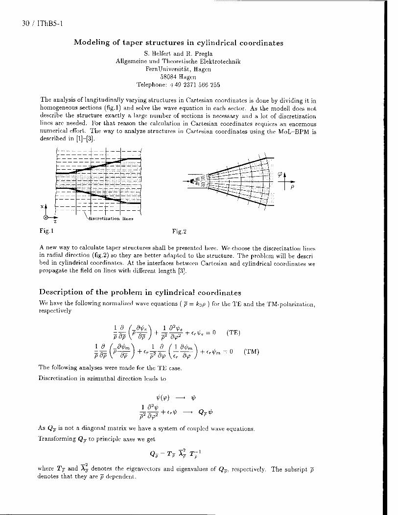
30 / IThB5-l
Modeling of taper structures in cylindrical coordinates S. Helfert and R. Pregla
Allgemeine und Theoretische Elektrotechnik FernUniversität, Hagen
58084 Hagen Telephone: +49 2371 566 255
The analysis of langitudinally varying structures in Cartesian coordinates is done by dividing it in homogeneous sections (fig.l) and solve the wave equation in each sector. As the modell does not describe the structure exactly a large number of sections is necessary and a lot of discretization lines are needed. For that reason the calculation in Cartesian coordinates requiers an enormous numerical effort. The way to analyze structures in Cartesian coordinates using the MoL-BPM is described in [l]-[3].
discretization lines
Fig.l Fig.2
A new way to calculate taper structures shall be presented here. We choose the discretization lines in radial direction (fig.2) so they are better adapted to the structure. The problem will be descri- bed in cylindrical coordinates. At the interfaces between Cartesian and cylindrical coordinates we propagate the field on lines with different length [3].
Description of the problem in cylindrical coordinates We have the following normalized wave equations ( p = k0p ) for the TE and the TM-polarization, respectively
pdp\p dp + €r=2
d<p2
l__ö_ f 1 dx/> ■f dp er d<p
The following analyses were made for the TE case.
Discretization in azimuthal direction leads to
+ eripe = 0 (TE)
+ eripm = 0 (TM)
H<P) tp
1 0V + £rV> Q»1P /J2<V
As Qj is not a diagonal matrix we have a system of coupled wave equations.
Transforming Qj to principle axes we get
Q-fi
TT h T.p -l
-^2 where Tj and A^- denotes the eigenvectors and eigenvalues of Qj, respectively. The subsript denotes that they are p dependent.

IThB5-2 / 31
The behaviour of some eigenvectors and eigenvalues (exactly the square root of the eigenvalues) is shown in fig.4 and fig.5 (structure fig.3).
6/xm
100/jm 500 /im
Fig. 3 Analyzed structure
100 200 300 400 500 600 z [mm] ^-
Fig.4a 1st mode (Cartesian coordinates)
t 1
■o i_ J [ o - T ] i
O Ü 1 j j : o T i I j
IO -
«? ~ ' j [
o - i . , , . i . . . .
250 350 450 550 650
p[jim] ► Fig.4b 1st mode (cylindrical coordinates)
Fig. 4 Behaviour of the eigenvectors
750 260 350 450 650 650
P In"»] —► Fig.4b 3rd mode (cylindrical coordinates)
760
3.15
250 360 450 650 650 750
pljunj ►
Fig. 5 Behaviour of the eigenvalues
250 350 450 650 p[jim]
650 750
The eigenvectors in cylindrical ccordinates are nearly constant whereas we have linear changes in Cartesian coordinates. For higher modes (e.g. the 3rd mode) special care has to be taken in the region where the transition from guided to evanescent mode takes place. The change of the eigenvalues is very small.
Procedure to compute the field propagation First we divide the structure in sections along p. In each section the eigenvectors and eigenvalues are assumed to be constant.
The transformation of the potential and the wave equation

32 / IThB5-3
1 6 f_dtp\ -2- n
leads to the solution for the transformed potentials
where Ho is the Hankel function of the order zero.
The propagation of the field in each section can then be calculated
VKPZ)
After the inverse transformation
we obtain the original field.
41,2)(Ap2)
Ho^Wi) V-(Pi)
H^ if p2 < Pl , H02) if Pl < p2
xp = Tip
Results
The results for the structure in fig.3 are shown in fig.6 and fig.7
1.000
t 0.998
S. 0.996 Q.
0 200 400 600 800 1000 z [mm] ^.
Fig.6 Propagation behaviour of the electric field
25 30 35 40 45 Steps in segment 2
Fig. 7 Transmitted power
50
The transmitted power depending on the number of steps in the taper is compared in fig.7 for the computation in cylindrical and Cartesian coordinates. It can be be seen that the convergence in cylindrical coordinates is much better than that in Cartesian coordinates.
As the number of lines in cylindrical coordinates is independent from the number of steps we have an immense decrease of CPU time in comparison to that in Cartesian coordinates (e.g. factor 40 if 50 steps are used).
References
[1] R. Pregla and J. Gerdes ,' New beam-propagation algorithm based on the method of lines ', in Technical Digest on Integrated Photonics Research, 1990, (Optical Society of America, Washington, D. C, 1990), Vol. 5, S. 29-30.
[2] J. Gerdes and R. Pregla, "Beam-Propagation Algorithm based on the Method of Lines", /. Opt. Soc. Am. B, vol. 8, pp. 389-394, Feb. 1991.
[3] R. Pregla, J. Gerdes, E. Ahlers, S. Helfert "Algorithm for Waveguide Bends and Vectorial Fields", in Techn. Digest on Integrated Photonics Research, 1992 (Optical Society of America, Washington, DC, 1992), Vol. 9, S.32-33.
Thursday, February 23, 1995
Passive Waveguides and Devices
IThC 1:30 pm-3:00 pm Salon 1
Julian B. Soole, Presider Bellcore

34 / IThCl-1
Application of dry etched magneto-optic buried channel waveguides to optical circulator
Akiyuki Täte, Naoto Sugimoto and Yujiro Katoh Opto-Electronics Laboratories, Nippon Telegraph and Telephone Corporation, Tokai-
Mura, Naka-Gun, Ibaraki, 319-11, Japan Telephone +81-292-87-7542, Facsimile +81-292-87-7882
1. Introduction Optical isolators and circulators are realized utilizing 45" Faraday rotation 1,2). Pure
or substituted yttrium iron garnet (YIG) film is used in infrared optical communications, because of its transparency and large Faraday effect. Substituted YIG film is grown by liquid phase epitaxy (LPE). In general, it has uniaxial magnetic anisotropy with its easy magnetization axis parallel to its substrate. Small planar magnets can provide sufficient in plane magnetization. However, large external magnetic fields are needed to attain perpendicular magnetization. Bulky cylindrical magnets are attached to conventional Faraday rotators, because the light travels in a direction perpendicular to their substrates. It is difficult to construct waveguides that are perpendicular to the surface. It is easy, with a planar structure, to grow undercladding, core and overcladding layers onsubstrates \ The required film thicknesses are several 100 urn for a perpendicular structure and several 10 um for a planar one. The planar structure allows not only the easy fabrication of Faraday rotators but also the compact integration of external magnetic circuits and magneto-optic waveguides into optical circuits.
There have been many reports on wet etched buried waveguides 4,5). The wet etching method has poor reliability and the size and shape of the patterned core strip lack uniformity. Moreover, the patterned cross section is far from rectangular in shape and this makes it difficult to design a waveguide. The dry etching method has higher reliability and uniformity and provides a rectangular shaped core cross section. In this report, we describe the first application of dry etched buried waveguides to optical circulators. 2. Principle of the optical circulator
The light entering port 1 is separated into p- and s-polarized light by polarization beam splitter (PBS) 1, as shown in Fig. 1. Each polarized beam is rotated 45° and -45* by a Faraday rotator and a reciprocal rotator, respectively. These two beams are collected by PBS 2 and emitted from port 4. The light entering port 4 is also separated into p- and s-polarized light by PBS 2. Each polarized light is rotated 45° by the Faraday and the reciprocal rotators. The polarization of the two beams is reversed by the travelling direction. These two beams are collected by PBS 1 and emitted from port 2, as shown in Fig. 1. This function is not affected by the polarization states of the incident light. By the same function, the light entering port 2 exits from port 3 and the light entering port 3 exits from port 1. 3. Configuration of the optical circulator
The circulator we fabricated had a Faraday rotator and two PBS parts, as shown in Fig. 2. Each PBS part consisted of a PBS cube prism, and two conventional and two polarization maintaining (PMF) single-mode fibers. The PBS cube prism is a conventional polarization separating prism. Each surface was antireflection (AR) coated at 1.55 p.m. A light beam enters the PBS through two single-mode fibers independent of polarization state and the separated polarization beams pass through PMFs holding their polarization state. An FC and an SC connector were attached at the ends of the single-mode fiber and the PMF, respectively. The polarization axes of the PMFs were matched as the SC connectors were connected. These connector end

IThCl-2 / 35
faces were physical contact polished and not coated. The Faraday rotator consisted of magneto-optic waveguides, PMFs and a magnet.
The magneto-optic buried channel waveguide was fabricated using Ar ion beam etching and LPE. The waveguide was 3 mm long and the thicknesses of the core and cladding layers were 4 urn and 6 pm, respectively. The overcladding layer was grown on the core after dry etching. The end faces were polished and AR coated. Each PMF was cemented to the waveguide end faces with UV-curable adhesive matching their polarization axis. A 8x8x2.3mm Sm-Co planar magnet was used to supply the magnetic field for the saturation. Its applied a magnetic field of 170 Oe to the waveguides. The polarization axes of the two PMFs were inclined at 45° to the surface plane of the waveguide, as shown in Fig. 2. The other ends of the fibers were attached to SC connectors. These connectors allowed polarization axis matched connection with the fibers from the PBS. This configuration enables PMFs to be used as reciprocal rotator. 4. Characteristics of the fabricated optical circulator
An edge emitted LED was used as a 1.55 pm light source, because its light power is polarization independent. Table I shows a result of transmitted light measurements. Table II shows details of the insertion loss. The average insertion loss, near-end and far-end crosstalk were 3.6, -15.5 and -16.4dB, respectively. The beam radius of the fiber and the waveguide at 1.55 pm was 5.3 pm and 4.4x2.9 pm, respectively. The dry etched depth of the core layer of the waveguides used in this study was 2.8 pm. The beam profile was deformed by this shallow etching. When a 4.4x2.9 pm elliptical beam profile was assumed, the loss due to elliptical core mismatch was estimated as 0.8dB at one end face 6). A circular beam profile was realized by forming a rectangular shaped core and the spot size of the waveguide beam could be matched to the PMF by adjusting the refractive index difference between the core and cladding layers. The insertion loss was reduced more than ldB by matching the light beam profiles of the PMF and the waveguide. Most of the near-end crosstalk was induced by reflection at the FC and SC connectors. It is well-known that the reflected light power can be lowered to less than -30dB by AR coating a connector. A near-end crosstalk of below -30dB is possible. Waveguides show extinction ratios around 20dB when they are inserted between a fiber-polarizer and a fiber-analyzer under a magnetic field larger than a saturation field. The far-end crosstalk can be improved by about -20dB by removing the axial misalignment between the PMF and the waveguide. It will be easy to realize a lower crosstalk when waveguides with a larger extinction ratio 7) are used. 5. Conclusion
We described the first application of dry etched magneto-optic buried channel waveguides to an optical circulator. The Faraday and reciprocal rotator array consisted of two such waveguides, four PMFs and one planar magnet. Two conventional PBS prisms were used as polarization light separators/couplers. The average insertion loss and far-end crosstalk at a wavelength of 1.55 pm was 3.6 and -16.4 dB, respectively, using a polarization independent light power source. References l)M.Shirasaki, H.Kuwahara and T.Obokata; Appl. Opt. 20, 2683('81) 2)M.Shirasaki, F.Wada, H.Takamatsu, H.Nakajima and K.Asama; Appl. Opt.23,3271('84) 3)N.Sugimoto, Y.Katoh and A.Tate; A.P.L. 63, 2744('93) 4)E.Pross, W.Tolksdorf, and H.Dammann; A.P.L. 52, 682('88) 5)S.Kaewsuriyathumrong, T.Mizumoto, H.Mak and Y.Naito; J. Lightwave Tech., 8, 177('90)
6)W. Bludau and R. Rosseberg; J. Lightwave Tech., LT-3, 294('85) 7)R. Wolfe, R. A. Lieberman, V. J. Fratello, R. E. Scotti and N. Kopylov; A. P. L. 56,
426('90)

36 / IThCl-3
port3 ")
non-reciprocal 45* rotator
'reciprocal .45° rotator
Fig.l Diagram of polarization states at each components
(P°rtl ) SMF =gy-^ ^ PMF PMF
( port3 )
=a> JH (port2 )
FC connector PBS <o> en ...~?
SC connector
Fig.2 Optical circulator configuration. PMF
cf Magneto-optic waveguide
=^^
^
Waveguide and fiber
Table I The result of transmitted light measurements
UV-curable adhesive cemented points
Table II Details of the insertion loss
Output port (dB)
m
t; o OH
3 & C
i—i
1 2 3 4
1 * -18.1 -20.1 -3.3
2 * -18.5 ^\^ -3.9 -19.6
3 -3.7 -20.5 ^^ * -20.1
4 -19.7 -3.5 *-19.8 \.
* near-end port
Item Loss (dB)
PBS insertion loss 0.5x2
SC connection loss 0.2x2
Waveguide/fiber connection loss 0.2x2
Waveguide Insertion loss 1.8
Total loss 3.6

IThC2-l / 37
Multimode Interference (MMI) Couplers in SOI (Silicon-on-insulator)
Thomas Zinke, Uwe Fischer, Klaus Petermann Institut für Hochfrequenztechnik, Technische Universität Berlin
Einsteinufer 25, D-10587 Berlin Tel.: +49-30-31426816, FAX:+49-30-31424626
Introduction Silicon based integrated optics is attracting an increasing amount of interest due to low inherent loss at 1.3 um and 1.5 um and to the potential for transforming VLSI techniques from microelectronics to integrated optics. Different schemes for waveguides based on silicon technology have been proposed and examined [1-3]. Kurdi et al. [4] proposed SOI and low losses of rib waveguides in different SOI-material (BESOI: bond and etch back SOI, SIMOX-SOI: separation by implantation of oxygen, ZMR: zone melting recrystallisation) have been reported [5]. The losses depend mainly on the Si top layer thickness (Fig. la). It is reasonable to choose waveguides with large cross sections (which remain single moded for certain geometries[6]), in order to achieve a high coupling efficiency to single mode fibres. An optimum height of H = 11 urn Si-top layer thickness has been determined by Beam Propagation Method for insertion losses smaller than 0.15 dB. A rib/substrate aspect ratio of r = 0.5 (Fig.lb).has been chosen, which guarantees monomode propagation with the best lateral confinement. Etching to a depth of 5.5 urn causes problems in separating waveguides accurately in directional couplers. In consequence we decided to realize multimode interference couplers [7-9], which allow larger waveguide spacings at the access regions.
Manufacturing Process The basic SOI-material consisted of BESOI-material with a top layer thickness of H = 11 um and a Si02 layer thickness of t = 2 urn as well as SIMOX-SOI with an epitaxially thickened top layer to H = 7.5 urn with a Si02 layer thickness of t = 0.4 urn. Rib waveguides have been dry etched to the half of the height H using an oxygen/CF4 process, resulting in an underetching of the Si02 mask of about 2 urn at each side of the waveguide. Before the optical measurements the samples were polished to optical quality using a diamond paste.
Curvature Losses Curvatures with varying radii have been realized on SIMOX material. Low losses until radii of 15 mm have been achieved (Fig.2) showing good agreement with the theoretical prediction of Marcatili [10].
MMI-Couplers MMI-Couplers are based on the assumption of a good field confinement under the waveguide rib, in that case the propagation constants ß of the first modes may be approximated by
2 -2 rf__ n- (y+ 1) n 2 2 ' o H WMM p00- ßQl
with ßov: propagation constant of the v-th mode, Ä: vacuum wavelength, WMMI: width of the coupler, H: height of the Si-top layer. The 3 dB state is achieved at 1.5 • Ln . In order to determine the optimum spacing s of the access waveguides, we developed a simple expression for the excess coupling losses as a function of spacing , width v^MMI of the coupler and width w of the access waveguide (Fig.3a).
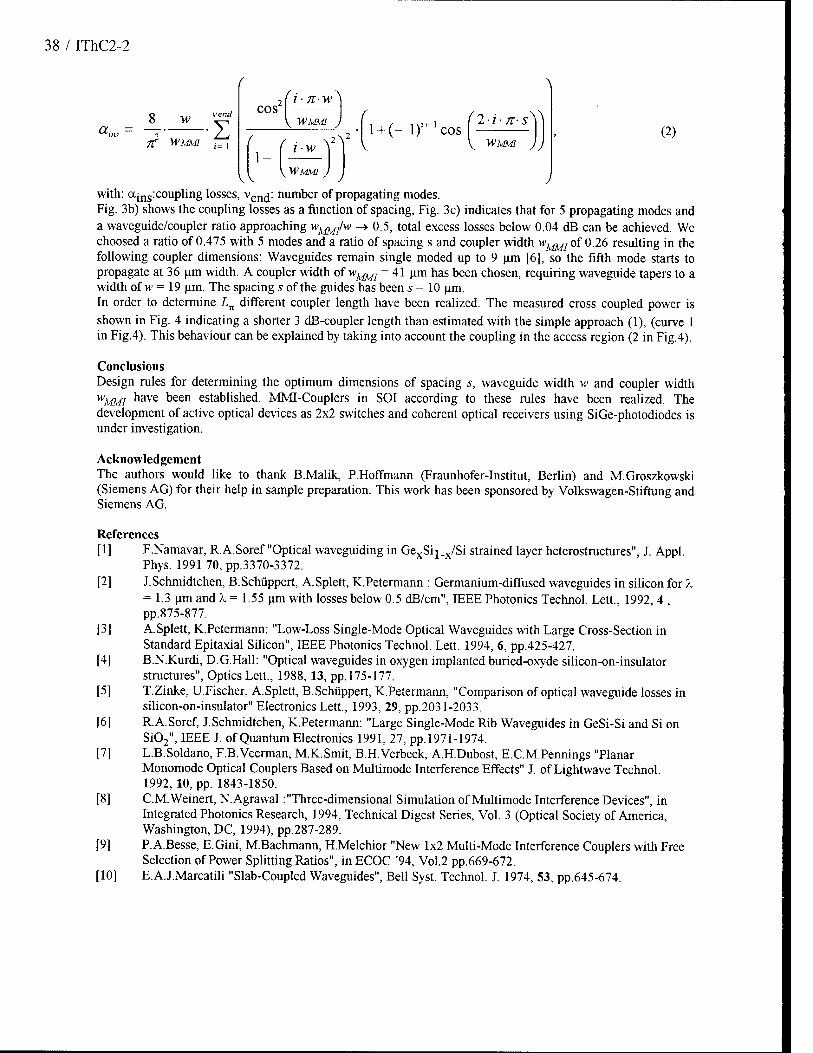
38 / IThC2-2
w a,.
ft WMM
vend
I i= 1
COS 2 1-71-W
WMM ) (
1- IW
\WMM
^Y l + (- l)'+1cos
2 • /' • n- s
WMM (2)
with: ams:coupling losses, vencj: number of propagating modes. Fig. 3b) shows the coupling losses as a function of spacing, Fig. 3c) indicates that for 5 propagating modes and a waveguide/coupler ratio approaching w^/w ->• 0.5, total excess losses below 0.04 dB can be achieved. We choosed a ratio of 0.475 with 5 modes and a ratio of spacing s and coupler width w^/of 0.26 resulting in the following coupler dimensions: Waveguides remain single moded up to 9 urn [6], so the fifth mode starts to propagate at 36 urn width. A coupler width of wMMI = 41 urn has been chosen, requiring waveguide tapers to a width of w = 19 um. The spacing 5 of the guides has been 5 = 10 urn. In order to determine Ln different coupler length have been realized. The measured cross coupled power is shown in Fig. 4 indicating a shorter 3 dB-coupler length than estimated with the simple approach (1), (curve 1 in Fig.4). This behaviour can be explained by taking into account the coupling in the access region (2 in Fig.4).
Conclusions Design rules for determining the optimum dimensions of spacing s, waveguide width w and coupler width WMMI have been established. MMI-Couplers in SOI according to these rules have been realized. The development of active optical devices as 2x2 switches and coherent optical receivers using SiGe-photodiodes is under investigation.
Acknowledgement The authors would like to thank B.Malik, P.Hoffmann (Fraunhofer-Institut, Berlin) and M.Groszkowski (Siemens AG) for their help in sample preparation. This work has been sponsored by Volkswagen-Stiftung and Siemens AG.
References [1] F.Namavar, R.A.Soref "Optical waveguiding in GexSii_X/Si strained layer heterostructures", J. Appl.
Phys. 1991 70, pp.3370-3372. [2] J.Schmidtchen, B.Schüppert, A.Splett, K.Petermann : Germanium-diffused waveguides in silicon for X
= 1.3 urn and X = 1.55 urn with losses below 0.5 dB/cm", IEEE Photonics Technol. Lett., 1992, 4 , pp.875-877.
[3] A.Splett, K.Petermann: "Low-Loss Single-Mode Optical Waveguides with Large Cross-Section in Standard Epitaxial Silicon", IEEE Photonics Technol. Lett. 1994, 6, pp.425-427.
[4] B.N.Kurdi, D.G.Hall: "Optical waveguides in oxygen implanted buried-oxyde silicon-on-insulator structures", Optics Lett., 1988, 13, pp. 175-177.
[5] T.Zinke, U.Fischer, A.Splett, B.Schüppert, K.Petermann, "Comparison of optical waveguide losses in silicon-on-insulator" Electronics Lett., 1993, 29, pp.2031-2033.
[6] R.A.Soref, J.Schmidtchen, K.Petermann: "Large Single-Mode Rib Waveguides in GeSi-Si and Si on Si02", IEEE J. of Quantum Electronics 1991, 27, pp.1971-1974.
[7] L.B.Soldano, F.B.Veerman, M.K.Smit, B.H.Verbeek, A.HDubost, E.C.M.Pennings "Planar Monomode Optical Couplers Based on Multimode Interference Effects" J. of Lightwave Technol. 1992, 10, pp. 1843-1850.
[8] C.M.Weinert, N.Agrawal: "Three-dimensional Simulation of Multimode Interference Devices", in Integrated Photonics Research, 1994, Technical Digest Series, Vol. 3 (Optical Society of America, Washington, DC, 1994), pp. 287-289.
[9] P.A.Besse, E.Gini, M.Bachmann, H.Melchior "New 1x2 Multi-Mode Interference Couplers with Free Selection of Power Splitting Ratios", in ECOC '94, Vol.2 pp.669-672.
[10] E.AJ.Marcatili "Slab-Coupled Waveguides", Bell Syst. Technol. J. 1974, 53, pp.645-674.

IThC2-3 / 39
10 E
3 5
9
\ • ZMR-SOI
♦ BE-SOI
■ SIMOX-SOI
V" 10
SMayef thickness, firn
Fig. la): Optical losses of SOI against silicon top layer thickness at X = 1.3 urn [5].
5 10 15
radius [mm]
Fig. 2: Excess curvature losses for different bend radii for SIMOX-SOI with a top layer thickness of 7.5 urn.
W
air (n=1.0) M
Si (n = 3.5)
Si-substrate
r*H i_y
Si02(n = 1.45)
Fig. lb) Structure of SOI rib waveguide [5].
theory neglecting coupling in access regions
theory considering coupling in access regions
E
2 / 1
0.8 ■
0.6 ■
0.4 \ A « ■ *v ■
0.2
n n «
W J
«
U --,.-
5 10 15
coupler length (mm)
20
Fig.4: Cross coupled power as a function of coupler length with theoretical prediction.
3a)
s '§ 1 w
MMI
1
' • ^
0.03
0.24 0.25 0.26
s/w MMI
0.27
S/WMM.=°-25
w/w MMI
Fig. 3 a) Principle structure of MMI-coupler. Fig.:3b) Coupling losses of each side of MMI-couplers as a function of waveguide spacing. Fig. :3 c) Coupling losses of each side of MMI-couplers as a function of coupler width and propagating modes.
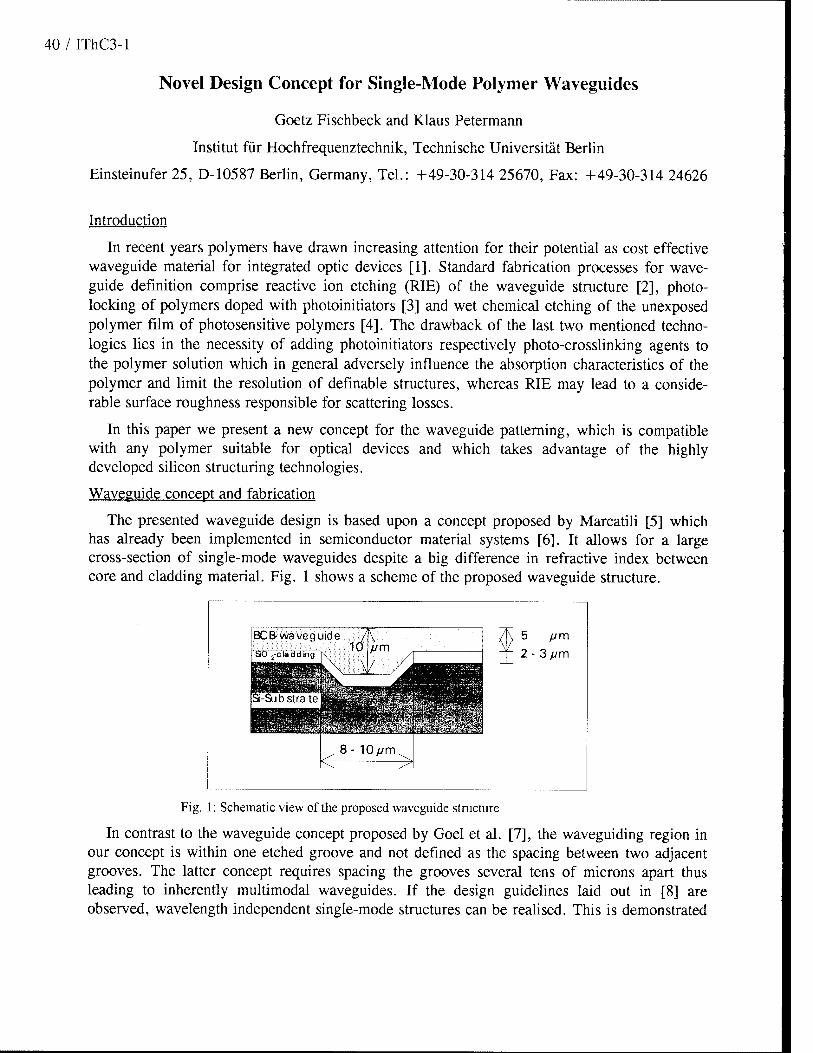
40 / IThC3-l
Novel Design Concept for Single-Mode Polymer Waveguides
Goetz Fischbeck and Klaus Petermann
Institut für Hochfrequenztechnik, Technische Universität Berlin
Einsteinufer 25, D-10587 Berlin, Germany, Tel.: +49-30-314 25670, Fax: +49-30-314 24626
Introduction
In recent years polymers have drawn increasing attention for their potential as cost effective waveguide material for integrated optic devices [1]. Standard fabrication processes for wave- guide definition comprise reactive ion etching (RIE) of the waveguide structure [2], photo- locking of polymers doped with photoinitiators [3] and wet chemical etching of the unexposed polymer film of photosensitive polymers [4]. The drawback of the last two mentioned techno- logies lies in the necessity of adding photoinitiators respectively photo-crosslinking agents to the polymer solution which in general adversely influence the absorption characteristics of the polymer and limit the resolution of definable structures, whereas RIE may lead to a conside- rable surface roughness responsible for scattering losses.
In this paper we present a new concept for the waveguide patterning, which is compatible with any polymer suitable for optical devices and which takes advantage of the highly developed silicon structuring technologies.
Waveguide concept and fabrication
The presented waveguide design is based upon a concept proposed by Marcatili [5] which has already been implemented in semiconductor material systems [6]. It allows for a large cross-section of single-mode waveguides despite a big difference in refractive index between core and cladding material. Fig. 1 shows a scheme of the proposed waveguide structure.
BCB-wave guide 5 fjm
2- 3//m
8- 10^/m
Fig. 1: Schematic view of the proposed waveguide structure
In contrast to the waveguide concept proposed by Goel et al. [7], the waveguiding region in our concept is within one etched groove and not defined as the spacing between two adjacent grooves. The latter concept requires spacing the grooves several tens of microns apart thus leading to inherently multimodal waveguides. If the design guidelines laid out in [8] are observed, wavelength independent single-mode structures can be realised. This is demonstrated
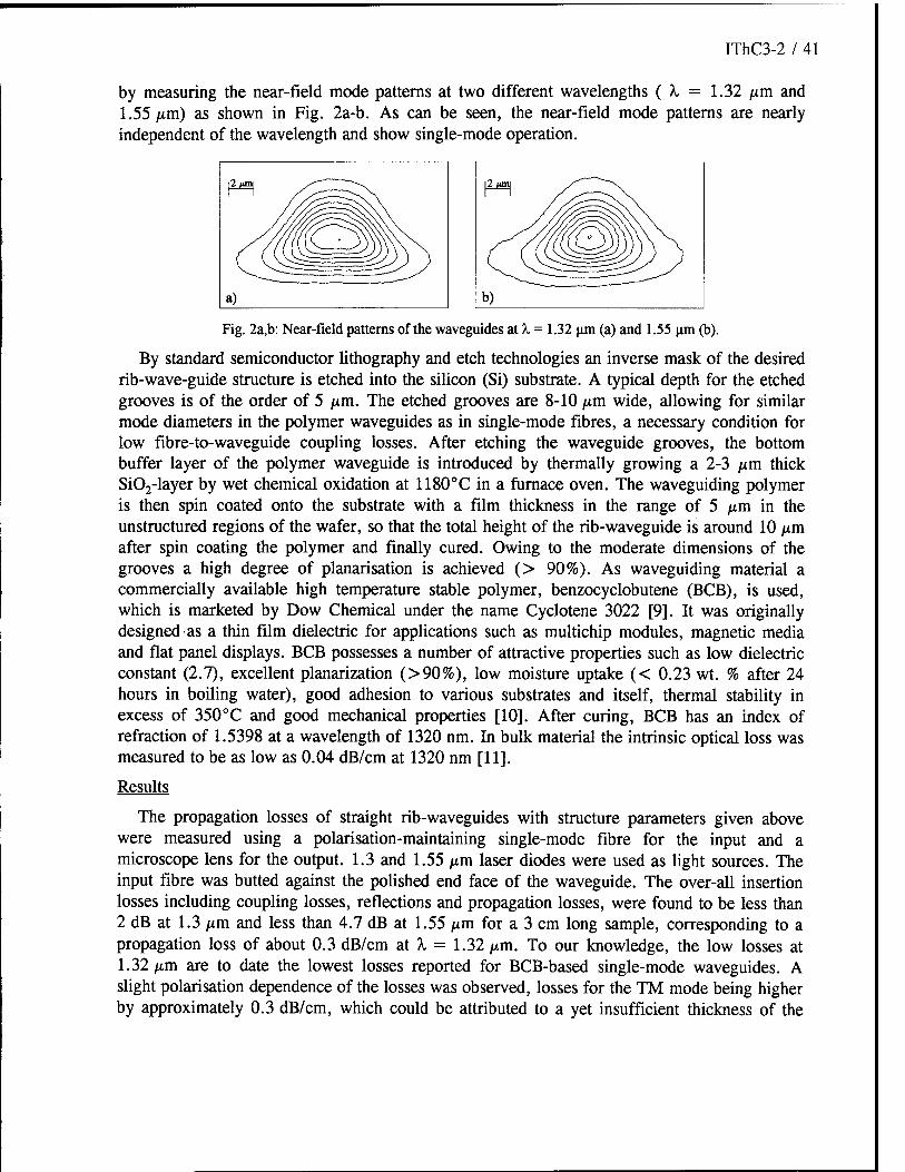
IThC3-2 / 41
by measuring the near-field mode patterns at two different wavelengths ( X = 1.32 fim and 1.55 fim) as shown in Fig. 2a-b. As can be seen, the near-field mode patterns are nearly independent of the wavelength and show single-mode operation.
Fig. 2a,b: Near-field patterns of the waveguides at X = 1.32 um (a) and 1.55 urn (b).
By standard semiconductor lithography and etch technologies an inverse mask of the desired rib-wave-guide structure is etched into the silicon (Si) substrate. A typical depth for the etched grooves is of the order of 5 jtm. The etched grooves are 8-10 fim wide, allowing for similar mode diameters in the polymer waveguides as in single-mode fibres, a necessary condition for low fibre-to-waveguide coupling losses. After etching the waveguide grooves, the bottom buffer layer of the polymer waveguide is introduced by thermally growing a 2-3 fim thick Si02-layer by wet chemical oxidation at 1180°C in a furnace oven. The waveguiding polymer is then spin coated onto the substrate with a film thickness in the range of 5 pm in the unstructured regions of the wafer, so that the total height of the rib-waveguide is around 10 fim after spin coating the polymer and finally cured. Owing to the moderate dimensions of the grooves a high degree of planarisation is achieved (> 90%). As waveguiding material a commercially available high temperature stable polymer, benzocyclobutene (BCB), is used, which is marketed by Dow Chemical under the name Cyclotene 3022 [9]. It was originally designed as a thin film dielectric for applications such as multichip modules, magnetic media and flat panel displays. BCB possesses a number of attractive properties such as low dielectric constant (2.7), excellent planarization (>90%), low moisture uptake (< 0.23 wt. % after 24 hours in boiling water), good adhesion to various substrates and itself, thermal stability in excess of 350°C and good mechanical properties [10]. After curing, BCB has an index of refraction of 1.5398 at a wavelength of 1320 nm. In bulk material the intrinsic optical loss was measured to be as low as 0.04 dB/cm at 1320 nm [11].
Results
The propagation losses of straight rib-waveguides with structure parameters given above were measured using a polarisation-maintaining single-mode fibre for the input and a microscope lens for the output. 1.3 and 1.55 ^m laser diodes were used as light sources. The input fibre was butted against the polished end face of the waveguide. The over-all insertion losses including coupling losses, reflections and propagation losses, were found to be less than 2 dB at 1.3 jum and less than 4.7 dB at 1.55 ^m for a 3 cm long sample, corresponding to a propagation loss of about 0.3 dB/cm at X = 1.32 fim. To our knowledge, the low losses at 1.32 ^m are to date the lowest losses reported for BCB-based single-mode waveguides. A slight polarisation dependence of the losses was observed, losses for the TM mode being higher by approximately 0.3 dB/cm, which could be attributed to a yet insufficient thickness of the

42 / IThC3-3
bottom buffer layer (2.3 ^m). Possibly the losses at 1.55/im could also be reduced by increasing the buffer layer thickness. Curved waveguides with a radius of curvature greater than 12.5 mm showed excess losses of less than 0.1 dB/90°bend.
Conclusion
A new design concept for wavelength-independent, single-mode polymeric waveguides is proposed, which is compatible with any polymer suited for optical applications, as long as it exhibits sufficient planarisation properties. Single-mode waveguides with a commercially available, high temperature stable (TG > 350 °C) polymer were demonstrated, showing propagation losses of about 0.3 dB/cm at 1.3 /im in 3 cm long straight waveguides.
References
[I] B.L.Booth: "Low loss channel waveguides in polymers", /. Lightwave Technology, 1989, Vol. 7, No. 10, pp. 1445-1453
[2] T. Matsuura, S. Ando, S Sasaki, F. Yamamoto: "Low loss, heat-resistant optical waveguides using new fluorinated polyimides", Electronics Letters, 1993, Vol. 29, No. 3, pp. 269-271
[3] N. Keil, B. Strebel, H. H. Yao, J. Krauser: "Applications of optical polymer waveguide devices on future optical communication and signal processing", SP1E Proceedings, 1991, Vol. 1559, R. Lessard "Photopolymer device physics, chemistry and applications II", pp. 278- 287
[4] C. Kane and R. Krchnavek: "Photodefinable benzocyclobutene as an optical waveguide material", Preprint from SPIE Proceedings, January 1994 "Optical interconnects II"
[5] E. Marcatili: "Slab-coupled waveguides", Bell Syst. tech. J., 1974, Vol. 53, pp. 645-674
[6] A. Splett and K. Petermann: "Low loss single-mode optical waveguides with large cross- section in standard epitaxial silicon", IEEE Photon. Technol. Lett., 1994, Vol. 6, No. 3, pp. 425-427
[7] S. Goel, J. Pincenti, D. Naylor: "Double V-groove ridge waveguides on a silicon substrate", Appl. Opt., 1993, Vol. 32, No. 3, pp. 318-321
[8] R. Soref, J. Schmidtchen, K. Petermann: "Large single-mode rib waveguides in GeSi-Si and Si-on Si02", IEEEJ. Quantum Electron., 1991, Vol. 27, No. 8, pp. 1971-1974
[9] A trademark of the Dow Chemical Company, Midland, MI 48674
[10] "Benzocyclotene technical data sheet", The Dow Chemical Company, Midland, MI 48674
[II] C. Langhoff, T. Stokich, B. Heistand: "Benzocyclobutene (BCB): A polymer system for passive optical interconnects", Proc. SPIE, Vol. 1849, 1993, pp. 336-341

IThC4-l / 43
REDUCING POLARIZATION DEPENDENCE in ASYMMETRIC COUPLER WAVELENGTH FILTERS
using BIREFRINGENCE COMPENSATION
R. J. Deri, M. A. Emanuel, F.G. Patterson, and S.P. Dijaili Lawrence Livermore National Laboratory, Livermore, CA 94550
WDM systems are creating demand for wavelength demultiplexers to extract a single wavelength channel from a stream of multi-wavelength data. A popular filter design employs an asymmetric directional coupler, either with or without a grating inserted between two coupled waveguides (fig. 1).[1-5]. This device selects a single wavelength channel, determined by the phase matching condition for the two coupled waveguides. Several such filters have been demonstrated using vertical couplers on III- V semiconductors, because this approach enables precise control of waveguide thicknesses and indices as well as monolithic integration.[2-5] Recently, integration of these filters with photodetectors and/or optical amplifiers [6-8] was demonstrated for receiver applications. A major obstacle to using such chips is the polarization sensitivity of the asymmetric coupler. Polarization-dependent shifts in filter wavelength AX0
exceed the filter bandwidth,[2-6] resulting in extreme polarization sensitivity AX0 =30nm incompatible with conventional single-mode fiber communications. The only reported polarization-insensitive device of this type[9] employs a doubly-periodic grating, and cannot be used in couplers without a grating. We previously proposed a birefringence compensation technique to eliminate polarization dependence in devices either with or without grating-assisted coupling, and used simulations to show that the approach involves fabrication tolerances.[10] Here we report the first experimental demonstration of these devices, validating the design concept proposed in ref. [10].
The polarization dependence of vertical asymmetric couplers on GaAs or InP results from the intrinsic waveguide birefringence, most of which occurs in the narrower waveguide. We replace the thicker waveguide core with a multiple quantum well (MQW), designed so the MQW birefringence compensates the upper guide birefringence.[10] Achieving practical tolerances requires additional design strategies to be presented at the conference. Based on these rules, we fabricated the AIGaAs filter of fig. 1, in which all cladding layers are Alo.5Gao.5As, the upper waveguide core consists of 0.1 u.m Alo.2Gao.8As sandwiched between two 0.09p.m compositionally graded layers, and the bottom waveguide core comprises an Alo.2Gao.8As/Alo.5Gao.5As MQW. with well:barrier thicknesses of 158Ä:159Ä (nominal). These epitaxial layers were grown by low-pressure MOCVD on a 2-inch GaAs wafer. The Alo.2Gao.8As composition was verified using room temperature photoluminescence (Ä.-PL=722.7nm, Al mole fraction within ±0.02). Thickness values were verified by SEM, which are shown in fig. 1. The principal difference between design and realized values are reduced upper guide thickness (0.23 vs. 0.28(im). Fabrication involved wet etching to remove the upper waveguide layer, followed by dry etching to define a rib guide input to the chip. The devices consist of an input rib waveguide using the lower (MQW) guiding layer, which uptapers to launch abroad beam into a 100u.m wide directional coupler section.
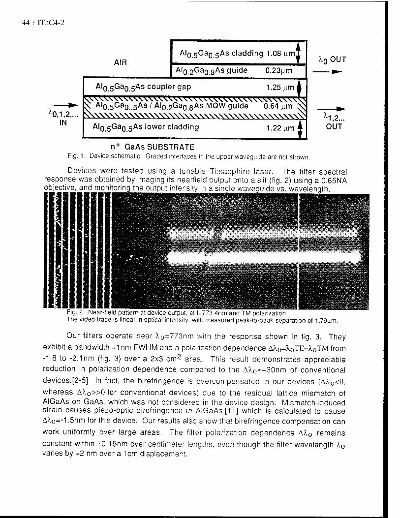
44 / IThC4-2
AIR A,0.5Ga0.5As c'adding 1.08 |im I
A,0.2Ga0.8As guide 0.23u.m
Al0 5Ga0 5As coupler gap 1.25 um I \ AlQ.5Gao.5As / Al0.2Gao.8As MQW guide 0.64 ^m XJ
A,0.5Ga0.5As lower cladding 1.22 um I
\nOUT
^1,2... OUT
n+ GaAs SUBSTRATE Fig. 1: Device schematic. Graded interfaces in the upper waveguide are not shown.
Devices were tested using a tunable Ti:sapphire laser. The filter spectral response was obtained by imaging its nearfield output onto a slit (fig. 2) using a 0.65NA objective, and monitoring the output intensity in a single waveguide vs. wavelength.
Fig. 2: Near-field pattern at device output, at 1=773.4nm and TM polarization. The video trace is linear in optical intensity, with measured peak-to-peak separation of 1.79u.m.
Our filters operate near X0=773nm with the response shown in fig. 3. They
exhibit a bandwidth *lnm FWHM and a polarization dependence A^0=^oTE-X.0TMfrom
-1.8 to -2.1 nm (fig. 3) over a 2x3 cm2 area. This result demonstrates appreciable reduction in polarization dependence compared to the AXo=+30nm of conventional
devices.[2-5] In fact, the birefringence is overcompensated in our devices (AA.o<0,
whereas A?iO»0 for conventional devices) due to the residual lattice mismatch of AIGaAs on GaAs, which was not considered in the device design. Mismatch-induced strain causes piezo-optic birefringence in AIGaAs,[11] which is calculated to cause AÄ.0=-1 .5nm for this device. Our results also show that birefringence compensation can
work uniformly over large areas. The filter polarization dependence A^0 remains
constant within ±0.15nm over centimeter lengths, even though the filter wavelength X0
varies by =2 nm over a 1cm displacement.
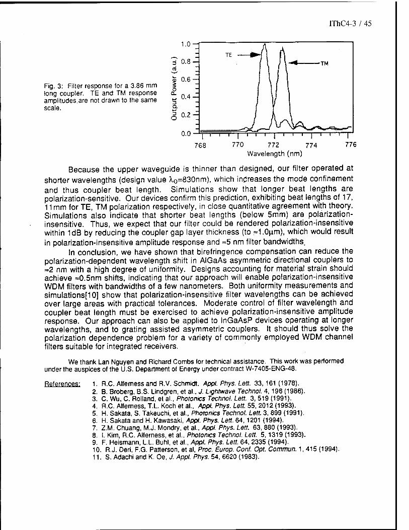
IThC4-3 / 45
Fig. 3: Filter response for a 3.86 mm long coupler. TE and TM response amplitudes.are not drawn to the same scale.
Wavelength (nm)
Because the upper waveguide is thinner than designed, our filter operated at shorter wavelengths (design value ko=830nm), which increases the mode confinement and thus coupler beat length. Simulations show that longer beat lengths are polarization-sensitive. Our devices confirm this prediction, exhibiting beat lengths of 17, 11 mm for TE, TM polarization respectively, in close quantitative agreement with theory. Simulations also indicate that shorter beat lengths (below 5mm) are polarization- insensitive. Thus, we expect that our filter could be rendered polarization-insensitive within 1dB by reducing the coupler gap layer thickness (to =1.0u.m), which would result in polarization-insensitive amplitude response and =5 nm filter bandwidths.
In conclusion, we have shown that birefringence compensation can reduce the polarization-dependent wavelength shift in AIGaAs asymmetric directional couplers to =2 nm with a high degree of uniformity. Designs accounting for material strain should achieve =0.5nm shifts, indicating that our approach will enable polarization-insensitive WDM filters with bandwidths of a few nanometers. Both uniformity measurements and simulations[10] show that polarization-insensitive filter wavelengths can be achieved over large areas with practical tolerances. Moderate control of filter wavelength and coupler beat length must be exercised to achieve polarization-insensitive amplitude response. Our approach can also be applied to InGaAsP devices operating at longer wavelengths, and to grating assisted asymmetric couplers. It should thus solve the polarization dependence problem for a variety of commonly employed WDM channel filters suitable for integrated receivers.
We thank Lan Nguyen and Richard Combs for technical assistance. This work was performed under the auspices of the U.S. Department of Energy under contract W-7405-ENG-48.
References: 1. R.C. Alferness and R.V. Schmidt. Appl. Phys. Lett. 33,161 (1978). 2. 8. Broberg, B.S. Lindgren, et al.. J. Lightwave Technol. 4,196 (1986). 3. C. Wu, C. Rolland, et al., Photonics Technol. Lett. 3, 519 (1991). 4. R.C. Alferness, T.L Koch et al.. Appl. Phys. Lett. 55, 2012 (1993). 5. H. Sakata, S. Takeuchi, et al., Photonics Technol. Lett. 3, 899 (1991). 6. H. Sakata and H. Kawasaki, Appl. Phys. Lett. 64,1201 (1994). 7. Z.M. Chuang, M.J. Mondry, et al.. Appl. Phys. Lett. 63, 880 (1993). 8. I. Kim, R.C. Alferness, et al., Photonics Technol. Lett. 5,1319 (1993). 9. F. Heismann, L.L. Buhl, et al., Appl. Phys. Lett. 64, 2335 (1994). 10. R.J. Deri, F.G. Patterson, et al, Proc. Europ. Conf. Opt. Commun. 1, 415 (1994). 11. S. Adachi and K. Oe, J. Appl. Phys. 54, 6620 (1983).
46 / IThC5-l
Refractive-Index Profile of Annealed Proton-Exchanged LiTa03
Channel Waveguides from White-Light Source Measurements
Robert F. Tavlykaev, David B. Maring, and Ramu V. Ramaswamy Photonics Research Laboratory, Department of Electrical Engineering
University of Florida, Gainesville FL 32611, Phone/Fax: 904-392-0990/4963
Introduction
Recently, there has been an increasing interest in studying the properties of annealed proton- exchanged (APE) structures in LiTa03 due to its large electro-optical and nonlinear coefficients, as well as a higher optical damage threshold than that of LiNb03. Previous studies have illustrated some of the anomalous features of waveguides formed in LiTa03 [1]. In this paper, we consider the most prevalent case for practical devices, namely, single-mode (around >»=1.31u.m) channel APE waveguides. We evaluate their profiles by using white-light source measurements performed over the wavelength range 900 nm - 1700 nm. Simplicity in acquiring the necessary experimental data makes the applied technique a convenient tool for analyzing waveguide structures.
Modeling of Profiles
To a large extent, a rigorous theoretical analysis of APE waveguides in LiTa03 is hindered since the phase diagram of this material is unknown. Some studies have suggested the possibility of obtaining buried profiles in just a single-step diffusion due to a nonlinear dependence of the refractive index on proton concentration [1]. As such, information on the shape of the waveguide profile is, in general, required to accurately predict the waveguide parameters for an arbitrary fabrication condition. However, the reported peculiarities, including an increase in the refractive index during initial stages of the post-exchange annealing process, have been shown to occur only at relatively high proton concentrations. For low concentrations that yield weakly-exchanged, low-mode, annealed waveguides, the refractive index increment monotonically decreases with increasing annealing time. The resulting profile can, therefore, be approximated by the profiles used previously in modeling APE waveguides in lithium niobate [2].
We have analyzed test structures consisting of arrays of straight channel APE waveguides with monotonically increasing widths. To model the waveguides, a numerical routine similar to that in ref.[3] has been used. It allows reconstruction of the waveguide profile using a measured near-field pattern of the fundamental mode of a waveguide with its channel width being in the middle of the range of single-mode regime. An optical spectrum analyzer with a built-in broad-spectrum light source was used to determine the cutoff wavelengths of each waveguide. The waveguide widths (denned as the mask channel width) corresponding to cutoff of the fundamental, Wb and first higher-order, W2, modes can then be determined for any given wavelength within the measured spectrum range. Near-field measurements with the use of a conventional set-up were performed (at X=1.31 u\m) to obtain the modal distribution of a single-mode waveguide with a channel width of W0 between Wj and W2, ensuring a well-confined fundamental mode as well as the applicability of the effective index method (EIM).
The numerical technique used in this effort is an iterative process that adjusts the parameters of the waveguide profile in order to match the computed Wj and W2 to those measured. First, a trial value for the propagation constant is assigned and the parameters of the ID effective index profile corresponding to the channel profile of width W0 are determined by matching the computed and measured modal fields as well as the computed and trial value of the propagation constant. This profile is then used in EIM to determine the 2D index profile. Afterwards, channel profiles for WY and W2 are computed by substituting these values into the functions modeling the width distribution of index profile. The modal properties of the two waveguides are then analyzed with the use of a conventional BPM. In contrast to [4], we have not used EIM to analyze cut-off conditions since it is not accurate at mode cut-off. After the computed values of Wj and W2 are compared to the measured values, the trial value of the propagation constant as well as the parameters of the modeling functions are adjusted and another iteration is performed to obtain a better match between the computed and measured values of Wj and W2.
IThC5-2 / 47
The iterations continue until the difference becomes less than 0.5fim.
Fabrication and Characterization of Waveguides
An array of channel waveguides with widths ranging from 2|im to 10um in 0.5-|xm increments was fabricated by exchanging a Z-cut LiTa03 substrate in pyrophosphoric acid for 18 min at 260°C. The channels were defined by using a tantalum mask which was etched off after the exchange. The substrate was annealed for 30 min at 300°C in air. Finally, the endfaces were polished to allow endfire coupling.
An HP 71451A optical spectrum analyzer (OSA) with a built-in broadband (900nm-1700nm) halogen optical source was used to characterize the waveguides in a manner similar to that of a white-light source technique [5]. The light from the source was coupled into a waveguide via a single-mode fiber connectorized to the OSA (Fig.l). The waveguide output was coupled to a multimode fiber connectorized to the OSA monochromator input. The spectrum of light passing through the waveguide was analyzed by sweeping the monochromator detection bandwidth (lOnm) over the entire wavelength range and automatically normalizing throughput by the spectrum of the light source (Fig.2) which was measured previously by directly coupling the input fiber to the output one. By offsetting the input single-mode fiber with respect to the waveguide, higher-order modes were excited. The corresponding transmission curve exhibits peaks corresponding to the modes of consecutive orders. The peak positions depend on the channel width (Fig.2a). As expected, the relative magnitudes of the peaks depend on the input fiber offset, as the corresponding overlap integrals change; however, the associated variation of the measured cut-off wavelengths (3dB-level) did not exceed 5 ran (Fig.2b). The results of measurements are summarized in Fig.3.
Results and Discussion
The profiles of APE waveguides have been modeled at X=1.31um. At this wavelength, the range of single-mode operation is confined by the values W^.Oum and W2 =8.4u\m (Fig.3). A waveguide of width W=6|im was chosen as being sufficiently far from the fundamental mode cut-off so that EIM can be applied. After performing the iterations described above, we obtained the computed values W1=2.8|Jm and W2=8.0um agreeing reasonably well with the measured values. We estimated that a variation of 0.2um in the values of Wj and W2 corresponds to a change of 1.5-10"4 in the effective mode index.
The reconstructed index profiles in width and depth are shown in Figs.4 and 5. Fig.4 also depicts the corresponding effective index profile. In Fig.6, we present the computed and measured modal distributions in the width and depth direction. As seen, they are in good agreement, however, we did not accept it as the only check of the accuracy of the profile modeling since the modal field is known to be relatively tolerant to a variation in the waveguide profile. To have an additional and more sensitive check, we independently measured, using a modified prism coupler technique, the difference N-^ between the effective mode index N of the fundamental mode and the bulk index n,. and compared to the computed values for different channel widths. We found that the evaluated value N-^ie=1.4-10"3 for the 6u\m-wide waveguide is in rather good agreement with the measured value 1.1 -10"3. Fig.7 shows continued agreement over a wide range (4-lOjim) of channel widths.
Conclusion
The profiles of APE waveguides in LiTa03 were evaluated by using white-light source measurements. The evaluated and independently measured propagation constants of the fundamental mode agree well. Experiments devised to obtain a direct measurement of waveguide profiles and to compare them with the evaluated distributions are currently in progress. A dispersion curve of the waveguide refractive- index increment is to be determined by reconstructing profiles at different wavelengths covering the spectral region 900nm - 1700nm of the OSA. Estimation of the accuracy will be discussed.
References 1. T. Yuhara, K. Tada, and Y. S. Li,/. Appl. Phys., 71, p. 3966,1992. 2. X.F. Cao, R. V. Ramaswamy, and R. Srivastava, /. Lightwave Technoi, LT-10, p.1302,1992. 3. R Tavlykaev, K. Kiickelhaus, and E. Voges, /. Opt. Comm., 15, p.71,1994. 4. C. De Bernardi et al, /. Appl. Phys., 68, p. 6513,1990. 5. J. E. Baran, Y. Silberberg, and P. Perlmutter, OFC/IOOC, TU02,1987.

48 / IThC5-3
whit light ■ pholodetecwr ;
LiTaC>3
Fig.l Schematic of experimental setup
-15
(a) f
-30
800 1000 1200 1400
Wavelength (nm) 1600
cut-off for 3rd mode 2nd mode fundamental
(b)ff -10
c g '8 -15 E
| -20
-30
: 3 1 1 ■ 1 I
2 i i ■ i i i
fundamental V: fnodes modes mode -
; V';-"' /r / \ -
' . ■ *
\ * 1 1 .A
800 1000 1200 1400 1600
Wavelength (nm)
Fig.2 Transmission curves: (a) channel width 6}im (solid) and 5|im (dashed); (b) fiber offset 5pm (dashed) and 10pm (solid).
1650
1550
"E 1450
^ 1350
O) 1250 c a) 13 1150 > ^ 1050
950
850
: 1 1 1 1 - 1 1 1 —: : fundamental ^ :
i- "^ ■ /
: 1 st-order^,^^^"'
r - r s-^ 2nd-order
i- 3rd ,- -"4th - : i i i i i i i
3 4 5 6 7 8 9 Waveguide mask width W (pm)
10
Fig.3 Cutoff wavelengths (3B-level) for the first 5 modes as a function of the channel width W.
- 2 0 2 4 6 X (Jim )
Fig.4 Waveguide index profile along the width direction for W=6pm (solid) and the corresponding effective index profile (dashed).
2 3
Y(nm ) Fig5 Reconstructed waveguide index profile along the
depth direction for W=6pm.
X,Yljim ) Fig.6 Normalized (unit power) width and depth intensity
profiles for W=6pm; measured (solid) and computed (dashed). 0.0025
0.0020
„0.0015 c
I
£ 0.0010
0.0005
0.0
1. II | || ' ' 1 ■ ' 1 1 | 1 I 1 1 | 1 1
** + ■ ; + '. - k ~ ■ ♦ I
; i /k
I
"mil 3 4 5 6 7 8 91011
Channel width (jam) Fig.7. Computed difference between mode index N and
bulk value as a function of W. Experimental data (triangles) were measured independently.
IThC6-l / 49
10 m long silica-based waveguide with a loss of 1.7 dB/m
Y. Hida, Y. Hibino, H. Okazaki and Y. Ohmori
NTT Opto-electronics Laboratories
162, Tokai-Mura, Naka-Gun, Ibaraki-Ken, 319-11, Japan
Tel: +81-292-87-7675, Fax : +81-292-87-7881
Recently many kinds of large-scale planar lightwave circuit (PLC) have been
developed for use in optical communication systems. Since the characteristics of large
scale PLCs depend on the losses in waveguides, PLC performance can be improved by
reducing such losses. The propagation losses in silica-based waveguides have been
evaluated by using long waveguides such as that shown in Fig. 1. The lowest loss value
ever reported with silica-based long waveguides is 3.5 dB/m [1]. This was obtained in a
1.6-m long waveguide with a relative index difference A of 0.75 %. It was deduced that
the main reason for the loss is the scattering ascribed to the fluctuation of the refractive
index and the core-cladding interface. This means that lower loss waveguides can be
fabricated using lower A waveguides, though these require larger bending radii, and
therefore a lager circuit size. This indicates that the minimum A value should be
determined by taking account of the size of the substrate on which the long waveguides are
laid out. Here we report the fabrication and loss characteristics of a 10-m long waveguide
with a A of 0.45 % which has a very low loss of 1.7 dB/m.
The layout of a typical long waveguide is shown schematically in Fig. 1. The input
light from the port at bottom left spirals counterclockwise, and after passing the center it
spirals clockwise and passes to the port at top right. The bending radius (/?), the number of
turns in one rotation direction (AO and the distance to the next core (D) determine the path
length and the circuit size. This meander configuration enables us to lay out long
waveguides of more than 1 m in length on a 4 - 5 inch Si wafer.
After making several trial designs of long waveguides on a 5 inch Si wafer, we
selected R = 15 mm and obtained a 10-m long waveguide pattern where N = 23 and D =
0.1 - 0.5 mm. The minimum A value and the corresponding core size were determined as
0.45 % and 8x8-9x9 ^.m2 respectively, by ensuring that the following two conditions
were met. One is that the excess bending loss is negligible at a wavelength X of 1.55 |im
and the other is that unexpected higher order modes are not excited at X = 1.3 (J.m. In fact
this waveguide does not strictly satisfy the single mode condition at 1.3 |J.m. But lower
propagation losses are expected under a quasi-single mode condition [2].
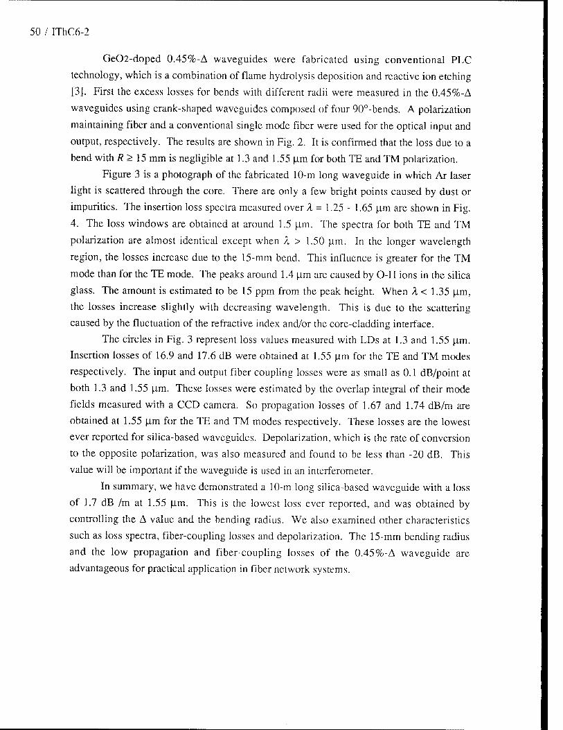
50 / IThC6-2
Ge02-doped 0.45%-A waveguides were fabricated using conventional PLC
technology, which is a combination of flame hydrolysis deposition and reactive ion etching
[3]. First the excess losses for bends with different radii were measured in the 0.45%-A
waveguides using crank-shaped waveguides composed of four 90°-bends. A polarization
maintaining fiber and a conventional single mode fiber were used for the optical input and
output, respectively. The results are shown in Fig. 2. It is confirmed that the loss due to a
bend with R > 15 mm is negligible at 1.3 and 1.55 |im for both TE and TM polarization.
Figure 3 is a photograph of the fabricated 10-m long waveguide in which Ar laser
light is scattered through the core. There are only a few bright points caused by dust or
impurities. The insertion loss spectra measured over A = 1.25 - 1.65 (im are shown in Fig.
4. The loss windows are obtained at around 1.5 (im. The spectra for both TE and TM
polarization are almost identical except when X > 1.50 |im. In the longer wavelength
region, the losses increase due to the 15-mm bend. This influence is greater for the TM
mode than for the TE mode. The peaks around 1.4 (im are caused by O-H ions in the silica
glass. The amount is estimated to be 15 ppm from the peak height. When X < 1.35 \±m,
the losses increase slightly with decreasing wavelength. This is due to the scattering
caused by the fluctuation of the refractive index and/or the core-cladding interface.
The circles in Fig. 3 represent loss values measured with LDs at 1.3 and 1.55 (im.
Insertion losses of 16.9 and 17.6 dB were obtained at 1.55 |im for the TE and TM modes
respectively. The input and output fiber coupling losses were as small as 0.1 dB/point at
both 1.3 and 1.55 |im. These losses were estimated by the overlap integral of their mode
fields measured with a CCD camera. So propagation losses of 1.67 and 1.74 dB/m are
obtained at 1.55 |im for the TE and TM modes respectively. These losses are the lowest
ever reported for silica-based waveguides. Depolarization, which is the rate of conversion
to the opposite polarization, was also measured and found to be less than -20 dB. This
value will be important if the waveguide is used in an interferometer.
In summary, we have demonstrated a 10-m long silica-based waveguide with a loss
of 1.7 dB /m at 1.55 (im. This is the lowest loss ever reported, and was obtained by
controlling the A value and the bending radius. We also examined other characteristics
such as loss spectra, fiber-coupling losses and depolarization. The 15-mm bending radius
and the low propagation and fiber-coupling losses of the 0.45%-A waveguide are
advantageous for practical application in fiber network systems.
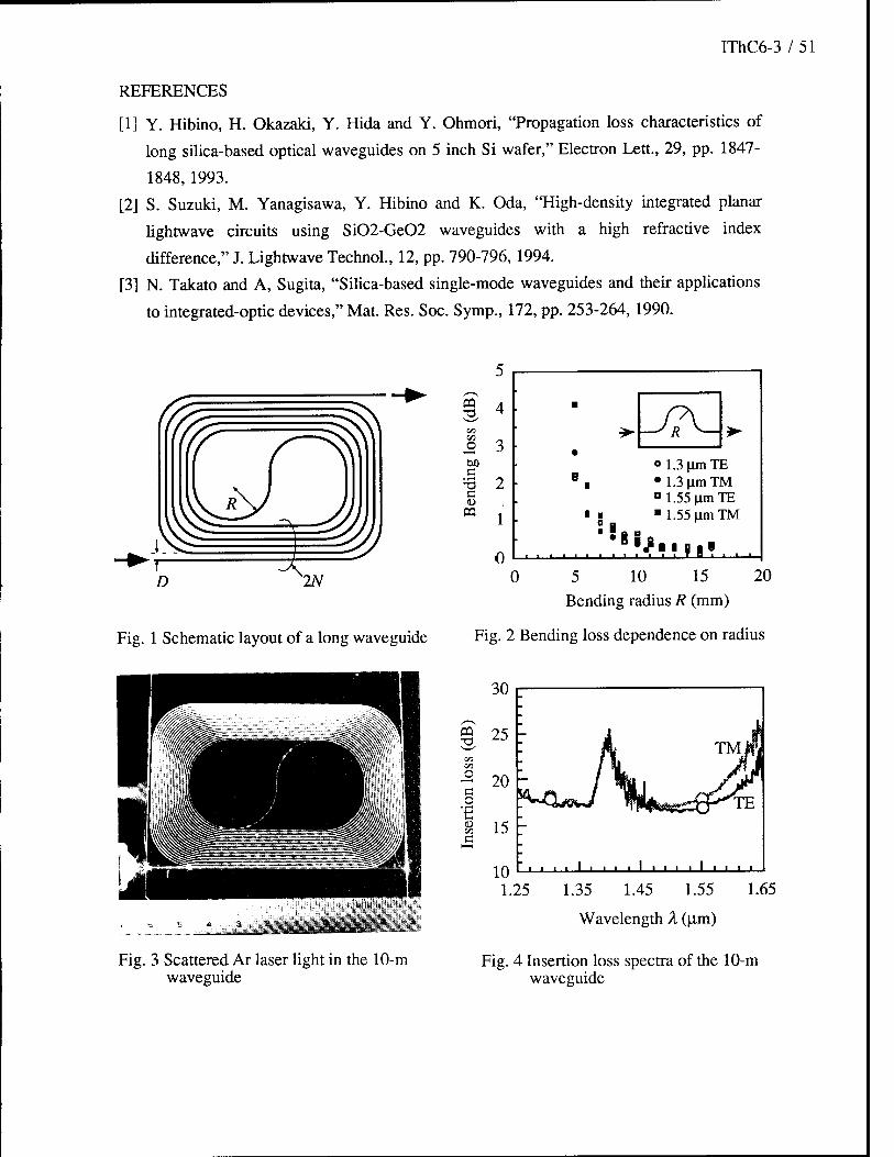
IThC6-3 / 51
REFERENCES
[1] Y. Hibino, H. Okazaki, Y. Hida and Y. Ohmori, "Propagation loss characteristics of
long silica-based optical waveguides on 5 inch Si wafer," Electron Lett., 29, pp. 1847-
1848,1993.
[2] S. Suzuki, M. Yanagisawa, Y. Hibino and K. Oda, "High-density integrated planar
lightwave circuits using Si02-Ge02 waveguides with a high refractive index
difference," J. Lightwave Technol., 12, pp. 790-796, 1994.
[3] N. Takato and A, Sugita, "Silica-based single-mode waveguides and their applications
to integrated-optic devices," Mat. Res. Soc. Symp., 172, pp. 253-264, 1990.
3
C
c ca
5
4 m
*- —' R ^— >■
3 • o 1.3|imTE
2 e I • 1.3 um TM
B 1.55 um TE
1 a I n ■ 1.55 um TM
0 1 1 1 1 1 1
•
i i i i i i T a i i—i—1_
0 5 10 15 20 Bending radius R (mm)
Fig. 1 Schematic layout of a long waveguide Fig. 2 Bending loss dependence on radius
O ! i
Fig. 3 Scattered Ar laser light in the 10-m waveguide
1.25 1.35 1.45 1.55 1.65
Wavelength X (|im)
Fig. 4 Insertion loss spectra of the 10-m waveguide

52 / NOTES
Thursday, February 23, 1995
Optoelectronic Modeling: 1
IThD 1:30 pm-3:00 pm Salon 4
Nadir Dagli, Presider University of California
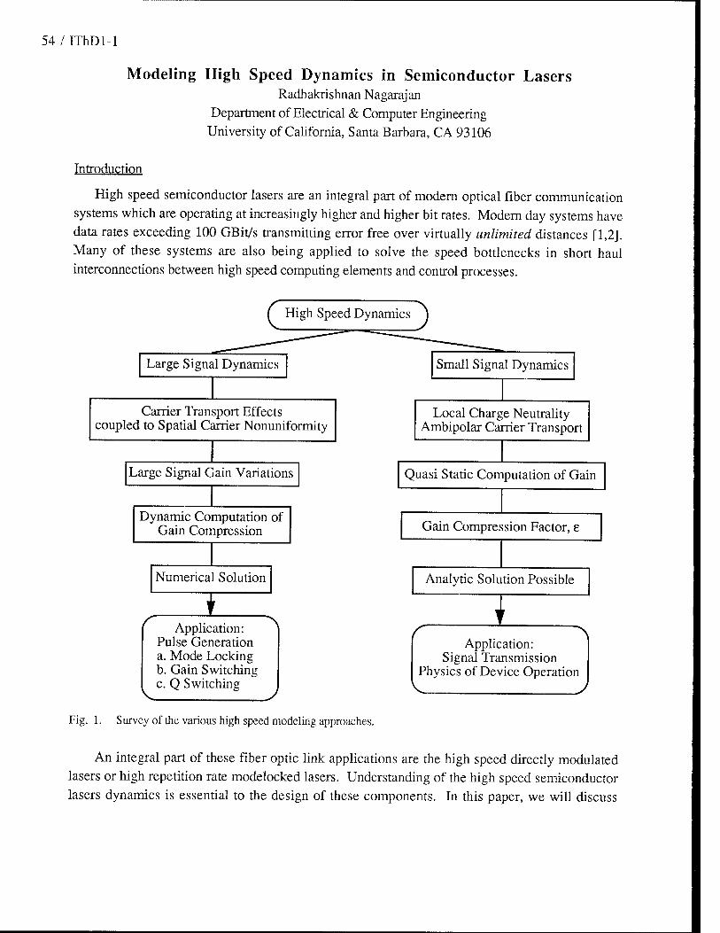
54 / IThDl-1
Modeling High Speed Dynamics in Semiconductor Lasers Radhakrishnan Nagarajan
Department of Electrical & Computer Engineering University of California, Santa Barbara, CA 93106
Introduction
High speed semiconductor lasers are an integral part of modern optical fiber communication systems which are operating at increasingly higher and higher bit rates. Modem day systems have data rates exceeding 100 GBit/s transmitting error free over virtually unlimited distances [1,2]. Many of these systems are also being applied to solve the speed bottlenecks in short haul interconnections between high speed computing elements and control processes.
f High Speed Dynamics j
Large Signal Dynamics
Carrier Transport Effects coupled to Spatial Carrier Nonuniformity
Large Signal Gain Variations
Dynamic Computation of Gain Compression
Numerical Solution
I Application:
Pulse Generation a. Mode Locking b. Gain Switching c. Q Switching
Small Signal Dynamics
Local Charge Neutrality Ambipolar Carrier Transport
Quasi Static Computation of Gain
Gain Compression Factor, e
Analytic Solution Possible
I Application:
Signal Transmission Physics of Device Operation
Fig. 1. Survey of the various high speed modeling approaches.
An integral part of these fiber optic link applications are the high speed directly modulated lasers or high repetition rate modelocked lasers. Understanding of the high speed semiconductor lasers dynamics is essential to the design of these components. In this paper, we will discuss

IThDl-2 / 55
some of the aspects of modeling high speed laser dynamics and their application to the design of
high speed lasers and systems [3].
Figure 1 shows a brief survey of the various approaches used to model high speed dynamics in semiconductor lasers. The type of modeling needed falls into two broad categories: large signal and small signal modeling. They vary a great deal in the amount of numerical computation required. The large signal models are more complicated and are generally accompanied by a higher level of sophistication in the results they can produce. Analytic solutions are generally only possible in the small signal regime, although one may make some assumptions about carrier and photon density variations in the laser cavity to obtain mathematically tractable solutions even in the
large signal case [4].
Generally, large signal modulation is used to characterize pulse generation in semiconductor lasers. The favored pulse generation techniques are modelocking, gain switching and Q switching. Small signal analysis has a surprisingly large area of usefulness as well. The general aim of this exercise is to obtain some concise analytic formulation of the problem so that the high speed design parameter space may be easily explored and a practical high speed device easily designed. This form of analysis is also used to model directly modulated laser transmitter links and produces surprisingly good results even though such links typically operate in the large signal regime.
Carrier Transport Effects T51
Carrier transport effects in high speed lasers, especially those with quantum well active regions, have received a considerable amount of attention lately. Early theoretical predictions and later experimental work have shown that lasers with quantum well active areas have enhanced differential gain over bulk lasers. This enhancement in the intrinsic differential gain led to predictions of increased modulation bandwidth in quantum well lasers. This enhancement in the modulation bandwidth proved to be elusive, because of the adverse effects of carrier transport.
The models that have been proposed to simulate the carrier transport effects in semiconductor lasers vary a great deal in mathematical sophistication. A complete large signal model includes a self consistent solution of the current continuity and Poisson equations to account for the drift and diffusion components of the current flow across the optical confinement layer and between the multiple quantum wells of the active region. The band bending resulting from the charge distribution under current injection will also require the simultaneous solution of the Schrodinger equation to compute the quantized energy levels, and the resulting density of states and bandfilling functions. Computing the current flow across semiconductor heterojunctions will require the use of thermionic emission theory. Thermionic emission theory is also used to compute the thermally activated carrier escape rate from the quantum well which is significant in devices operating at room temperature. Although the thermionic process is in opposition to carrier capture and degrades the overall carrier capture efficiency, it is essential for carrier transport between the quantum wells. Another transport process of interest in a multiple quantum well system is tunneling between the quantum wells. Additionally, we will also have to consider the quantum
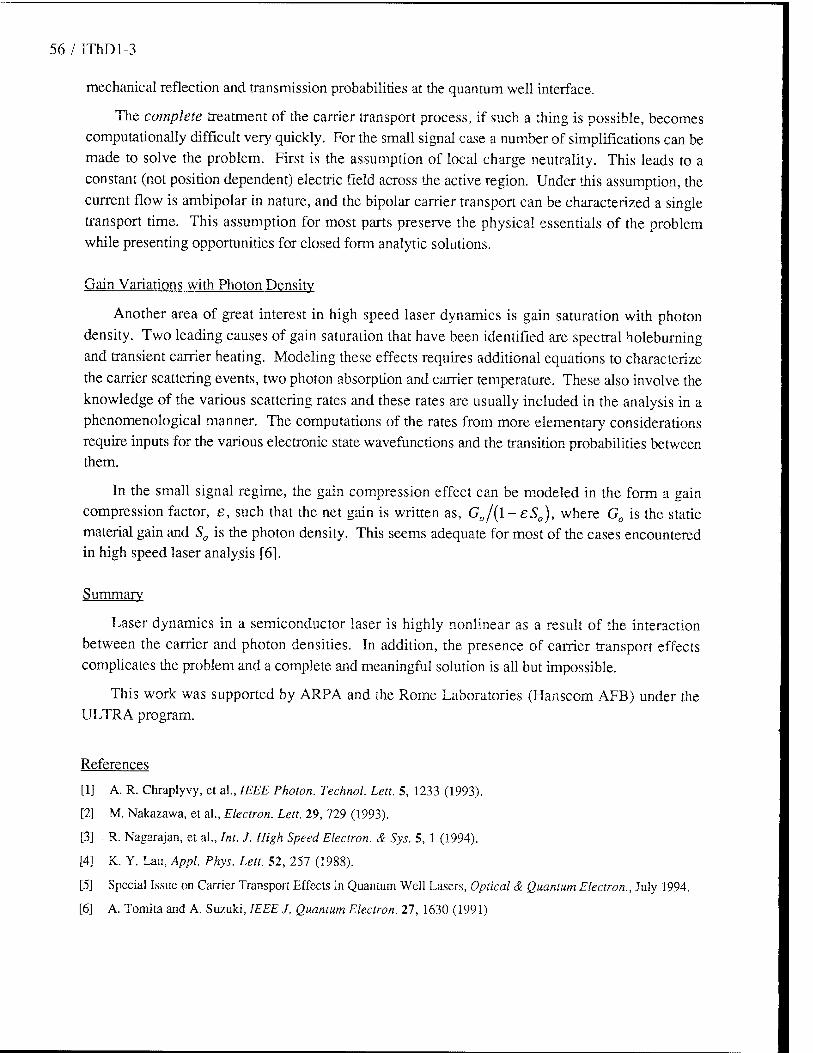
56 / IThDl-3
mechanical reflection and transmission probabilities at the quantum well interface.
The complete treatment of the carrier transport process, if such a thing is possible, becomes computationally difficult very quickly. For the small signal case a number of simplifications can be made to solve the problem. First is the assumption of local charge neutrality. This leads to a constant (not position dependent) electric field across the active region. Under this assumption, the current flow is ambipolar in nature, and the bipolar carrier transport can be characterized a single transport time. This assumption for most parts preserve the physical essentials of the problem while presenting opportunities for closed form analytic solutions.
Gain Variations with Photon Density
Another area of great interest in high speed laser dynamics is gain saturation with photon density. Two leading causes of gain saturation that have been identified are spectral holeburning and transient carrier heating. Modeling these effects requires additional equations to characterize the carrier scattering events, two photon absorption and carrier temperature. These also involve the knowledge of the various scattering rates and these rates are usually included in the analysis in a phenomenological manner. The computations of the rates from more elementary considerations require inputs for the various electronic state wavefunctions and the transition probabilities between them.
In the small signal regime, the gain compression effect can be modeled in the form a gain compression factor, e, such that the net gain is written as, G0/(l-eS0), where G0 is the static material gain and S0 is the photon density. This seems adequate for most of the cases encountered in high speed laser analysis [6].
Summary
Laser dynamics in a semiconductor laser is highly nonlinear as a result of the interaction between the carrier and photon densities. In addition, the presence of carrier transport effects complicates the problem and a complete and meaningful solution is all but impossible.
This work was supported by ARPA and the Rome Laboratories (Hanscom AFB) under the ULTRA program.
References
[1] A. R. Chraplyvy, et al., IEEE Photon. Technol. Lett. 5, 1233 (1993).
[2] M. Nakazawa, et al., Electron. Lett. 29, 729 (1993).
[3] R. Nagarajan, et al., Int. J. High Speed Electron. & Sys. 5, 1 (1994).
[4] K. Y. Lau, Appl. Phys. Lett. 52, 257 (1988).
[5] Special Issue on Carrier Transport Effects in Quantum Well Lasers, Optical & Quantum Electron., July 1994.
[6] A. Tomita and A. Suzuki, IEEE J. Quantum Electron. 27, 1630 (1991)
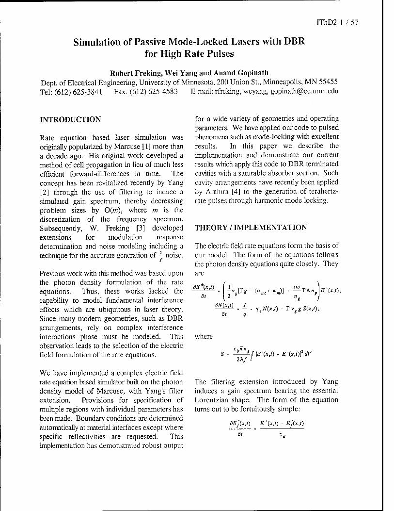
IThD2-l / 57
Simulation of Passive Mode-Locked Lasers with DBR for High Rate Pulses
Robert Freking, Wei Yang and Anand Gopinath Dept. of Electrical Engineering, University of Minnesota, 200 Union St., Minneapolis, MN 55455 Tel: (612) 625-3841 Fax: (612) 625-4583 E-mail: rfreking, weyang, [email protected]
INTRODUCTION
Rate equation based laser simulation was originally popularized by Marcuse [1] more than a decade ago. His original work developed a method of cell propagation in lieu of much less efficient forward-differences in time. The concept has been revitalized recently by Yang [2] through the use of filtering to induce a simulated gain spectrum, thereby decreasing problem sizes by 0(m), where m is the discretization of the frequency spectrum. Subsequently, W. Freking [3] developed extensions for modulation response determination and noise modeling including a technique for the accurate generation of - noise.
Previous work with this method was based upon the photon density formulation of the rate equations. Thus, these works lacked the capability to model fundamental interference effects which are ubiquitous in laser theory. Since many modern geometries, such as DBR arrangements, rely on complex interference interactions phase must be modeled. This observation leads to the selection of the electric field formulation of the rate equations.
We have implemented a complex electric field rate equation based simulator built on the photon density model of Marcuse, with Yang's filter extension. Provisions for specification of multiple regions with individual parameters has been made. Boundary conditions are determined automatically at material interfaces except where specific reflectivities are requested. This implementation has demonstrated robust output
for a wide variety of geometries and operating parameters. We have applied our code to pulsed phenomena such as mode-locking with excellent results. In this paper we describe the implementation and demonstrate our current results which apply this code to DBR terminated cavities with a saturable absorber section. Such cavity arrangements have recently been applied by Arahira [4] to the generation of terahertz- rate pulses through harmonic mode locking.
THEORY / IMPLEMENTATION
The electric field rate equations form the basis of our model. The form of the equations follows the photon density equations quite closely. They are
dE\x,t)
at
\ vjrg- (a.,* oj] -Yhn. E\xj),
dN(x,t)
at y,N(x,t) - TvggS(x,t)y
where
£onng
2hf f\E'(x,t) ♦ E-(x,tfdV
The filtering extension introduced by Yang induces a gain spectrum bearing the essential Lorentzian shape. The form of the equation turns out to be fortuitously simple:
dE}(x,t) E%,t) - E}(x,t)
at i,
58 / IThD2-2
A cavity is discretized automatically into cells from regions specified by the user. Material and operating parameters must be specified for each region. The preceding equations are solved at each discretization once per time step. The solutions are exact within the framework of the model. Since the method is direct, the calculation at each time step is completed rapidly.
Propagation, with proper reflection and transmission at boundaries dictates the spatial interaction of the rate equations. Reflection and transmission coefficients must be determined for both forward and reverse travelling waves with proper attention to phase changes at the boundaries. While this is normally determined from the indices of refraction, specific facet reflectivities may be specified. Since each cell could potentially be specified with a different index, the speed of propagation must be calculated for every cell. The shortest propagation time through any cell determines the time step. Though this implementation does not demand that all cell lengths allow for full propagation of cell contents into neighboring cells in one time step, choosing cell lengths according to this guideline eliminates a source of error. Yang's filtering extension is embedded within the outlined structure. Due to propagation, the filtering acts in the spatial dimension as well as in time.
RESULTS
Inclusion of interference effects was a primary goal of this work. Central to the phenomena of interference in laser theory is the Fabry-Perot etalon characterization. As a baseline, transmission through a simple cavity as a function of wavelength has been examined with this simulator. The results of these runs are identical with theory. These results are presented in fig. 1.
8503 time (ps)
Figure 1 Fabry-Perot etalon transmission plot for 30%, 64%, and 87% mirror reflectivities shows theoretical behavior.
Because DBR sections must be discretized at a quarter wavelength in the material, the time step, determined by propagation time across a cell, is minute — on the order of femtoseconds. Thus, any cavity with a DBR section will take considerably longer to simulate than a cavity without such minuscule detail. Since long runs tend to expose numerical instability, accurate results for reflection from a quarter-wave stack demonstrated not only the intended capability of the code, but also the inherent, long-term stability of the method. Results of reflection from different depth quarter-wave stacks are shown in fig. 2.
8o.07
7o*07
60.07
5». 07
4». 07
3«.07
2e.07
1«.07
0
■STACK2' STACKS'
'5TACK16; 'STACK32'
I-
I -
700 750 wavgltngth (nm)
Figure 2 Left hand side of reflection plot for quarter wave stacks tuned to 850nm with 2, 8, 16, and 32 cells (1, 4, 8, and 16 periods). Input intensity is le+08.
Mode-locking modeling capabilities have been demonstrated from the shaping influences of a

IThD2-3 / 59
saturable absorber section even in photon density based code as by Yang [2] and W. Freking [5]. Several standard mode-locking and CPM structures have been successfully simulated by the present electric field based implementation. Having simulated these simpler structures with our code, we turned to the recent claim made by Arahira of terahertz-rate optical pulses generated through harmonic mode- locking from a cavity with a saturable absorber and a DBR section at one end. We have simulated a structure similar to Arahira's. The cavity length has been shortened considerably to accommodate our computational resources. When an identical cavity is simulated without the DBR section the mode-locked pulse rate is exactly that of the round trip time of the cavity, as expected. When a short DBR section is inserted at the end, terahertz-rate pulses appear. Several different cavity lengths were sampled with the simple cavity always exhibiting a pulse rate determined by the round trip time and the DBR capped cavity always holding independently constant in rate. See fig. 3.
time (ps)
Figure 3 Self-pulsated terahertz-rate pulses overlaid with output from similar cavity without DBR.
CONCLUSIONS
We have described a formulation of the electric field rate equation problem that is robust and stable under diverse cavity geometries and operating parameters. Interference effects have been demonstrated, exhibiting the utility and power of this formulation. We have applied this code to examine the recent claims of terahertz- rate optical pulses from DBR terminated cavities with a saturable absorber section. Mode-locking has been simulated in photon density based code, but those implementations cannot model phase interactions. Our complex electric field simulation has permitted this DBR geometry to be examined in the mode-locking context.
REFERENCES
[1] D. Marcuse, "On Approximate Analytical Solutions of Rate Equations for Studying Transient Spectra of Injection Lasers," J. Quantum Electron., vol. QE-19, pp. 1397-1406, 1983. [2] W. Yang and A. Gopinath, "Study of passive mode locked lasers by time domain simulations," Appl. Phys. Lett., vol. 63, pp. 2717-2719, 1993. [3] W. Freking, W. Yang, and A. Gopinath, "External cavity semiconductor laser for modulation beyond its relaxation oscillation frequency," MTT-94 Conf. Proc. [4] S. Arahira, et. al., "Terahertz-rate optical pulse generation from a passively mode-locked semiconductor laser diode," Optics Lett., vol. 19, no. 11, pp. 834-835,1994. [5] W. Freking, W. Yang, and A. Gopinath, "Study of the stability of passive mode-locked lasers using numerical simulation," IPR-94 Conf. Proc, pp. 360-361.
60 / IThD3-l
Integratable Semiconductor Laser Phase Conjugate Mirrors
W.M.Yee and K.A.Shore
Bath University
School of Electronic and Electrical Engineering
BATH BA2 7AY ,UK
Tel: + 44 225 826272 ; Fax : + 44 225 826305
Multiwave mixing in above-threshold semiconductor laser structures can be utilised to generate phase conjugate signals in both reflection and transmission modes.The phase conjugate reflectivities of the structures may be used to narrow the linewidth of a laser diode transmitter.This paper proposes a novel laser diode structure which is capable of direct integration with the laser transmitter and which can be configured to yield enhanced broad band phase conjugation.The device may also be operated as a stand-alone phase conjugate repeater where its phase conjugate transmission properties may be exploited to effect four-wave mixing cancellation in multi-channel optical fibre systems.
Calculations have been performed using a numerical model of nearly degenerate multiwave mixing in above-threshold laser diodes taking account of longitudinal variations in the nonlinear interactions [l].The model can, in particular, be used to optimise the phase conjugation characteristics of laser diodes having longitudinally varying inversion carrier density [2]. The model has already been used to establish opportunities for enhanced phased conjugation (in both reflection and transmission modes) in asymmetric laser diodes having unequal facet reflectivities [3]. In this work attention has been given to the multi-wave mixing properties of twin-section laser diodes where longitudinal tailoring of the current injection can be used to advantage to obtain high phase conjugate reflectivity .
Consideration is first given to a symmetric twin-section laser diode with facet reflectivities of 0.3 and using basic device parameter values given in [1] . The two sections of the device are pumped with current densitiess Ja and J^ whose values indicated below are normalised to the device transparency current .Figure 1 shows the conjugate reflectivity for three current pumping conditions : (a) Ja = JD
= 2.20 ;(b) Ja = 2.25 , J5 = 2.19 ; (c) Ja .= 2.15 , JD = 2.21 . In all cases the optical power per facet is 7.7 mW. It is seen that when the two sections are biased differently the conjugate reflectivity decreases due to a phase mismatch consequent to the carrier-density induced refractive index changes in the two sections.lt is also observed that the relaxation resonance is enhanced when the probe injection is incident at the higher gain section (Figure 1 b ) and is highly damped when the probe injection is incident at the lower gain section (Figure lc). A uniform conjugate reflectivity can thus be obtained using a two-section laser diode with the probe incident at the low gain section.
Figure 2 shows the conjugate reflectivity versus frequency detuning for the same biasing conditions as Figure 1. However for Figures 2b and 2c asymmetric mirror reflectivities are utilised.Comparing curves b and c from Figures 1 and 2 it is seen that conjugate reflectivity enhancements of 7-8 dB can be obtained using asymmetric-facet laser diodes rather than symmetric structures.In addition , the FWM bandwidth is enhanced in the asymmetric device. Higher FWM bandwidths can be obtained by biasing the lasers further above threshold.
It is noted that laser diodes subject to phase conjugate optical feedback may exhibit novel dynamical behaviour [2,3] which may be amenable to investigation in an integrated structure incorporating a target laser diode coupled to a twin section semiconductor laser diode phase conjugate mirror.
References
1. W.M.Yee and K.A.Shore, J. Opt. Soc. America B , 11,1211-1218,1994 2. L.N.Langley and K.A.Shore, Optics Letts., 18, 1432-1434 ,1993 3. L.N.Langley and K.A.Shore , IEE Proc.- Optoelectronics, 141,103-108,1994
IThD3-2 / 61
n I r
o 10 o m o ^- ro ro CM CM
(gp) A^]Ajp9ü9J ajDßnfuoo

62 / IThD3-3
i i i—i I I i i i i i i i i I i t i i l i .1 i i O
i i I i i i i
o o
N
a CD a
CD
o d CD Z5 CT
(gp) X^iAip9|pj QpßnfuoQ

IThD4-l / 63
Modeling and Design of Traveling-Wave Quantum Well Waveguide Electron-Transfer Modulators
M. M. Mihailidi, J. E. Zucker, and M. N. Khan
AT & T Bell Laboratories Crawfords Corner Road
Rm 4F-327 Holmdel, NJ 07733
Tel: (908) 949-5557 Fax: (908) 949-8988
High-speed electrooptic modulators and switches are in demand for many applications including high-data-rate optical communication, analog microwave optical links, and optical time division demultiplexing. Semiconductor quantum well electroabsorption modulators can be made very compact, -100 um, which provides capacitance-limited electrical bandwidths as high as 40 GHz1 with drive voltages on the order of a few volts. On the other hand, semiconductor Pockels effect modulators in which the velocities of optical and electrical waves are well-matched can achieve even higher bandwidths2 but require larger drive voltages. It is therefore important to explore how the low-voltage advantage of semiconductor quantum wells might be combined with a velocity-matched traveling wave structure to produce a low-power consumption modulator with the capability to reach millimeter wave frequencies.
In this paper, we present a quasi-static model for the microwave refractive index of quantum well electron transfer waveguide modulators which allows us to explore microstrip, coplanar, and hybrid geometries. The potential distribution for particular waveguide configurations is determined via finite difference solution of Laplace's equation using the relaxation method. This yields the charge distribution, which then yields a value for the microwave refractive index n^. We show that by modifying the existing quantum well waveguide modulator structure, we can significantly alter n^ to approach the optical refractive index no. With a near-velocity-matched design, the 3dB electrical modulator bandwidth can be extended to over 40 GHz.
Fig. la shows the standard Barrier Reservoir and Quantum Well Electron Transfer (BRAQWET) modulator cross-section. Voltage is applied between the top n-type InGaAs cladding layer and the n-InP substrate, with the field concentrated across the d=0.839 urn thick quantum well region. Fig. lb shows the calculated static potential profile V. The accumulated
InGaAs/lnGaAIAs Quantum Weils Fig.l. Cross section of (a)
InGaAs/lnGaAIAs BRAQWET modulator on doped InP substrate (b) calculated potential contours where we have used dielectric constants e= 12.61 for InP, 12.71 for InAlAs, and 12.81 for the quantum wells. The calculation uses a 400 X 200 array with rectangular grid size of 0.08 X 0.1 urn. In the calculation, w= 2.5 urn, dciaP 0.5 urn, t= 0.25 urn, and the substrate is 400 urn thick.
64 / IThD4-2
d=0.839 jim
w=2.5 p.m /w=5.0 [xm
(a)
10 20 30 40 50 Frequency (GHz)
Fig. 2. Calculated microwave index as a function of frequency obtained by varying (a) waveguide rib width w and (b)quantum well thickness d for the modulator structure shown in Fig. 1. We have taken the value of the conductivity as o=1..25 X105 Q 'm'.
charge Q is determined by integration of the normal displacement component Q = eeÄE-dS . This yields a value for
the capacitance per unit length C of this geometry as well as C0, the capacitance in the absence of dielectrics3. The
microwave index is yi - L C —— • Neglecting fringe fields, we have C
■ A) C0
•££ W
0 — and the inductance per unit length a
D L= ßü~, where D= dclad +d+8, and 8 is the frequency-dependent skin depth 8 = (Ju0/Tfj)"1/2(/)"l/2. Thus we
obtain the microwave index as a function of frequency for various microstrip geometries as shown in Fig. 2. We have found that this simple method successfully accounts for measured n,, values in the literature and also agrees with computational results obtained by much more sophisticated models4. Fig. 2 shows that we can decrease the microwave index (to approach the optical index, IV- 3.3) somewhat by decreasing the rib width w or the increasing the thickness of quantum wells d, but there is still a significant velocity mismatch because of the large skin-depth at low frequency. The effect on modulation bandwidth is shown in Fig. 3. where we plot the response as a function of frequency for various values of n^ in a 0.8 cm long device. CO Q
Fig. 3 Calculated modulation response as a function of drive frequency for waveguide width 2.5 urn, length 1 cm, thickness of quantum wells 0.839 urn, and various values of the microwave index n^. The optical index no=3.3.
0 10 20 30 Drive Frequency (GHz)
40
IThD4-3 / 65
w InGaAs/lnGaAIAs Quantum Wells
Fig. 4 Coplanar microstrip quantum well waveguide modulator on semi-insulating substrate.(a) layer structure (b) calculated potential distribution. Microwave index of 3.28 is achieved withs= 1.0 (im, d=0.839 urn, t=0.25 urn, and w=2.5 urn.
Frequency-dependent conductor loss is included in the calculation of Fig. 3 as 00=2.53 X 105 cm"1/"2 assuming that the electrode thickness is greater than the skin depth (5=2.9 urn at/=l GHz). Fig. 3 shows that for the BRAQWET structure on doped substrate (as shown in Fig.l) the 3 dB electrical modulator bandwidth is < 10 GHz.
In order to obtain velocity match over a larger frequency range we propose the structure shown in Fig. 4. The use of semi-insulating InP:Fe substrate effectively eliminates the frequency dependence of the microwave index due to skin depth effect and reduces the microwave index. The calculated microwave index for this structure is 3.28 which (as shown in Fig. 3) results in a 3dB modulation bandwidth of 40 GHz.
In summary, we have developed a model for high-speed traveling-wave modulators that employ semiconductor quantum wells. Results based on our calculation method are in good agreement with the spectral domain technique4 analysis of similar structures. The proposed high- frequency modulator is expected to have high bandwidth and low operating voltage.
REFERENCES
R G. Walker, J. Quan. Electron. 27, 654
1 "High-speed InGaAs/InAlAs multiple quantum well optical modulators with bandwidth in excess of 40 GHz at 1.55 urn," K. Wakita, I. Kotaka, O. Mitomi, H. Asai, Y. Kawamura and M. Naganuma, Conference on Lasers and Electro Optics 1990, p.CtuC6. 2 "High-speed III-V semiconductor intensity modulators,' (1991). 3 "Technique for velocity-matched traveling-wave electrooptic modulator in AlGaAs/GaAs," M. N. Khan, A. Gopinath, J. P. G. Bristow, and J. P. Donnelly, Trans. Microwave Theory and Tech. 41,244 (1993). 4 "Analysis of a new microwave low-loss and velocity matched iii-v transmission line for traveling wave electrooptic modulators," I. Kim, M. R T. Tan, S. Y. Wang, J. Lightwave Technol. 8,728 (1990).
66 / IThD5-l
Intensity noise transfer in interferometric wavelength converters
X. Pan and T. L. Koch AT&T Bell Labs, Holmdel, NJ 07733, USA
Abstract— Interferometric semiconductor optical amplifier A simple analysis reveals that the gain of the probe Gp is wavelength converters are shown to have strong influence on given by the relative intensity noise of the converted channel. Ways of improving the noise performance of the wavelength converter are discussed.
Gn I, p,out
h = fo(g)fi(Ag)IpM (1)
I. Introduction Wavelength conversion in semiconductor optical amplifiers (SOAs) employing the gain saturation (GS) effect has been demonstrated [1], [2]. Recently, wavelength conversion us- ing SOAs in a Mach-Zehnder configuration has also been demonstrated [3]. These interferometric devices utilize the phase delay in a SOA that results from the linewidth en- hancement factor and GS due to input optical power. The variation in phase delay is converted into intensity modula- tion at the output of the interferometer. With typical val- ues of the linewidth enhancement factor, a Mach-Zehnder wavelength converter can operate at lower signal power level. Interferometric devices also achieve higher extinc- tion ratios in the converted channel. The device can also operate in either a data inverting or non-inverting mode.
In this paper, we first propose a new Mach-Zehnder wavelength converter configuration and then present the first study of the noise characteristics of the device.
II. Static analysis Figure 1 is a schematic of the device under consideration. The signal (pump) and the probe propagate in opposite di- rections and the need for filtering out the original signal at the probe output port is therefore eliminated. The other advantage of the present configuration is that it maximizes the ability of the signal to unbalance the interferometer by injecting the signal to saturate only one SOA.
signal
out
fo(g) = '2\J{Vi - Vl){m - Tll)l3 ■ e6 (2)
probe
Fig. 1 Schematic of the Mach-Zehnder wavelength converter
Let rji be the coupling coefficients of the Y-junctions as shown in Fig. 1 and gi the single pass gain of the SOAs.
/i(A.g) cosh(A# + (?) + cos(aAg + <p0) (3)
where I„ and /„ are the input and output probe - 91+.12 js tjle average gajn 0f tne
1p,in ^n^ Lp,out
power, respectively, g —
SOAs and Ag = ^^ the difference between them. 9 is a parameter related to the coupling coefficients and is given by 0 = 2 In ^^ffitrjz) ■ <PQ is a phase factor accounting for the small path difference of the two arms of the in- terferometer. Here a is the linewidth enhancement factor and is assumed to be identical for both SOAs. It is also assumed that the Y-junctions have no excess loss.
In (1) the probe gain Gp is determined by two terms which are additive in logarithmic scale. The first term f0 is a function of the average gain g of the SOAs and accounts for the 'pure' gain saturation effect. The second term fl
is a function of the difference in the gain between the two amplifiers Ag and represents the interference effect. To maximize the extinction ratio of the probe channel, the lower intensity state should correspond to the minimum of the probe gain Gp. In Fig. 2 the probe gain Gp is plotted against Ag for three different tp0 values: 0, 7r/2 and T. In the calculation, we set rji = rj2 = rj3 = 0.5, a = —6, and <72 is held constant at 20 dB.
-S0 5 9i -9j(dB)
Fig. 2 Gp as a function of Ag = 31-32

IThD5-2 / 67
The results indicate that, even without any control of (f0, an extinction ratio of 15-20 dB for the probe chan- nel is possible for an amplifier gain variation < 5 dB. </i and hence Ag decrease with the pump power, due to GS. Fig. 2 shows that the probe output can either be in-phase (non-inverting wavelength conversion) or out-of-phase (in- verting wavelength conversion) with the pump signal, de- pending on the operating condition. Higher extinction ratio can be obtained for inverting wavelength conversion. This asymmetry is mainly due to the fact that /0 decreases with the pump.
RINi„0„t = A(n)RINIp_,n + B(Q)RINIsi
where
A(Q) = 1 — Ip,in9N Gim
(7)
2(QB1 + jQ) (1 + /2(A«7))
+ G2(l-Vi) 2(fiS2+jft)
(l-/2(Aff)) (8)
III. Noise properties of the device B(n) Is,in9N Gi(l-T3)
(1 + /2(A«?)) (9)
In this section, we study the transfer of intensity noise from the inputs of the pump and probe to the probe out- put. Intensity noise in the pump causes the optical gain and phase delay of the upper branch SOA to fluctuate in Fig. 1. The interferometer converts the phase fluctua- tion into intensity noise of the probe at its output port. We call this intensity noise conversion from the pump to the probe. This is inevitable in a wavelength converter as the operation of the device relies on GS. Similarly, if the intensity of the probe is strong enough to saturate the am- plifiers, the original relative intensity noise (RIN) of the probe will either be suppressed or enhanced when pass- ing through the interferometer. We will call this intensity noise amplification.
Two other sources contribute to the noise of the probe: carrier shot noise and amplified spontaneous emission (ASE) in the SOAs. Treatment of these two effects are not given here, but the results will be presented at the conference.
For time scales long compared with the transit time through the SOAs, and eg> » 1, the carrier rate equa- tions read
dNi_
8N2
dt
vhexe,
= Ji - Ä(Wi) - Gifoilp,in + (1 - m)Is,in)(4)
J2 - R(N2) - G2(l - m)Ip,in
Gi (gi + ai)eg
(5)
(6) huigiV
with V being the volume of the active region of the SOAs and Too the photon energy. J; is the current pumping rate to the SOAs, R the spontaneous recombination rate and ai the single pass waveguide loss in the SOAs.
Using a standard small signal analysis, we get the rela- tion between the input and output RINs.
where fljg, is a 3-dB bandwidth determined by the car- rier life time
fiB1 = Ä + Glwhl/p]in + (i_^jS]in](io)
&B2
dN
dR(N2)
dN + G2gN(l - r]i)IPiin
/2(Aff) = /i(Ag)
(11)
(12) /i(Aff)
giv is the derivative of the single pass gain gi with re- spect to the carrier density. The RIN enhancement factors A and B have low pass characteristics with bandwidth de- termined by the carrier life times of the amplifiers. In the high frequency limit, A = 1 and 5 = 0, i.e., there is no conversion of RIN from signal to probe and the RIN of the probe at output equals that at the input. Also, A(Q,) —*■ 1 if I, p,zn 0; and B(ü) — 0 if Is 0, th ere is no amplification/conversion of RIN when the wavelength converter is linear.
In Fig. 3, the probe gain is shown on the left axis against the input signal power. The input power of the probe is 0.1 mW. The bias to the lower SOA is such that g2 = 20 dB. The bias to the upper OS A is set such that Gp is at its minimum when IStin = 0. The a parameter value is -6 and ipa =Q. Other parameter values amplifiers are typical for bulk SOAs. For 7Sij„ = 0, the probe gain has a minimum of-0.4 dB. For a input power of about 0.2 mW, the probe gain has a maximum of 18.6 dB. An extinction ratio of about 19 dB is obtained for a input signal power change of 0.2 mW. On the right axis, the RIN enhancement fac- tors A and B for Q = 0 are shown. Near the probe gain minimum, the RIN of the probe is greatly amplified. How- ever, the conversion from signal RIN to that of the probe is insignificant due to the low signal power (cf. (9)). At the probe gain maximum, the RIN amplification is about

68 / IThD5-3
8 dB. At this point, the intensity noise conversion from the pump to the the probe is completely suppressed. In this example, the probe output changes in-phase with the input signal.
0.00 0.10 0.20 0.30 Signal input (mW)
0.40
Fig. 3 Probe gain Gp (Left axis) and the RIN enhancement factors
A and B at DC (Right axis) as functions of the input power of the signal.
In Fig. 4, we have set the bias such that the probe gain is a minimum when ISiin is at its maximum of 0.4 mW. Now the probe output is out-of-phase with the pump. The figure shows that the probe gain increases from -0.4 dB to a maximum of 24 dB when the signal input decreases from 0.4 mW to 0.032 mW. At the maximum gain, the probe RIN is amplified by 11 dB. Again, at this point, there is no conversion from signal RIN to that of the probe. Near the probe gain minimum (ISiin < 0.4 mW), there is a strong amplification/conversion of the RIN.
0.00 0.40 0.10 0.20 0.30
Signal input (mW)
Fig. 4 Same as in Fig. 3 except now the bias to the upper amplifier
is set such that the probe gain Gp is at its minimum when /s ;„ = 0.4 mW.
Comparing Figs. 3 and 4, we see that the intensity noise conversion is much reduced when the wavelength converter is operated in the non-inverting mode. This is also more desirable from the optical network point of view. To max- imize the extinction ratio and to reduce the effect of in- tensity noise conversion/amplification, the power swing of the pump input should be adjusted to produce just enough
gain saturation for the probe gain Gp to change from the minimum to a maximum.
IV. Conclusion
Wavelength conversion using gain saturation effect in an interferometric configuration is analyzed. The intensity noise of the original probe may be enhanced or suppressed by the wavelength converter, depending on the operating point. This effect is reduced if the intensity of the probe is low. There is conversion of intensity noise from the pump to the probe. The conversion efficiency is critically dependent on the operating point. With proper biasing of the optical amplifiers and the proper power levels for the input signal, the intensity noise can reduced. These issues may be critical to the application of wavelength converters in a cascaded WDM network.
References
[1] B. Glance, J. M. Wiesenfeld, U. Koren, A. H. Gnauck, H. M. Presby, and A. Jourdan, "High performance optical wavelength shifter," Electron. Lett., vol. 28, pp. 1714-1715, Aug. 1992.
[2] J. M. Wiesenfeld and B. Glance, "Cascadability and fanout of semiconductor optical amplifier wavelength shifter," IEEE Photon. Ttchnol. Lett., vol. 4, pp. 1168- 1171, June 1992.
[3] T. Durhuus, J. Joergensen, B. Mikkelsen, R. Peder- sen, and K. Stubjkaer, "All optical wavelength con- version by SOA's in a Mach-Zehnder configuration," IEEE Photon. Technol. Lett., vol. 6, pp. 53-55, Jan. 1994.
Thursday, February 23, 1995
Automation of Optoelectronics Packaging
IThE 3:30 pm-5:00 pm Salon 1
W. Jack Tomlinson, Presider Bellcore
70 / IThEl-1
Progress Report on the ARPA/NCAICM Automated Optoelectronics Packaging Project
Donald E. Bossi United Technologies Photonics
1289 Blue Hills Avenue Bloomfield, CT 06002
Phone: (203) 769-3014, FAX: (203) 769-3007
At its 1993 Optical Communications Roadmap Workshop, the Optoelectronics Industry Development Association (OIDA) voted low-cost packaging to be the most critical issue facing the U. S. optoelectronics industry today. The costs associated with pigtailing and packaging operations presently represent greater than 60% of the total cost of packaged optoelectronic (OE) modules. As other elements in the manufacturing process are reduced in cost, the costs associated with pigtailing/packaging will become an even greater percentage, reaching as high as 90% of the total cost for high-volume markets.
Many of the low-cost packaging methods developed for high-volume electronic devices, such as automated die attach and automated wire bonding, can be easily applied to OE devices. However, the process of coupling and attaching single-mode or polarization-maintaining optical fibers to OE components involves sub-micron alignment tolerances and other mechanical difficulties for which there are no low-cost manufacturing processes. In fact, the sub-micron fiber-positioning and attachment procedures are presently carried out manually by highly trained technicians, resulting in a costly, low- throughput process.
This paper describes a 24-month ARPA/NCAICM-sponsored program, launched in April 1994, that seeks to substantially reduce the costs associated with pigtailing optoelectronic components by developing a modular, cost-effective manufacturing station for automated attachment of optical fibers to a variety of OE components. The automated manufacturing station for coupling and attaching optical fiber to optoelectronic components will be: versatile and user friendly, low cost (<$100k production cost target for a single attachment station), and sufficiently modular and generic to find widespread application throughput the field of OE component manufacturing. Progress toward this goal will be reported in the presentation.
Figure 1 illustrates the synergistic team of optoelectronic component manufacturers, optical equipment manufacturers, and experts in automation, manufacturing, optoelectronic packaging, and machine vision that has been assembled to address the goals of this program. The team will specify, design, build, test, and integrate into OE-device production a modular cost-effective station for automated attachment (or pigtailing) of optical fibers to OE components. The pigtailing station will be comprised of three functional sub-systems or modules that perform the following tasks: fiber preparation, coarse-fine alignment and attachment, and parts handling and feeding. The following discussion provides a brief technical description of each of these three functional modules.

IThEl-2 / 71
OE COMPONENT MANUFACTURERS
United Technologies Photonics Integrated-optics manufacturer,
Program / resource management
Ortel Corporation Laser-diode and photodiode
manufacturer.
GOAL Versatile, low-cost machine for high-volume, automated
fiber pigtailing
PIGTAILING MACHINE DESIGN TEAM
Lawrence Livermore Automated fiber-alignment technology, Program / resource management, Technology transfer.
MIT Manufacturing Institute Flexible automation technology, Low-cost positioner technology, Design for manufacturability.
Newport/Klinqer Manufacturer of optical-test and automated-alignment equipment.
EQUIPMENT MANUFACTURER
Figure 1. Automated Pigtailing Team
The fiber preparation module will prepare optical fiber for attachment to OE devices or modules. The machine will accept a spool of fiber, cut the fiber to a specified length, strip the buffer material from the ends of the fiber, and cleave the fiber endfaces. The machine will then load the prepared fibers onto small spools or other appropriate medium that can be easily handled by the automated pigtailing machine.
The Automated Coarse-Fine Alignment and Attachment Module represents the enabling technology for the automated pigtailing station. With the high accuracy required for efficient optical coupling, this module will quickly align and attach fibers to optoelectronic components. In particular, the module will utilize a relatively low-cost coarse-fine positioning system in conjunction with several forms of electronic feedback to perform sub-micron fiber-to-OE device alignment within one minute. The station will utilize a machine-vision system developed at Lawrence Livermore to locate the end of a prepared fiber and coarsely position the fiber endface within several microns of a pre- specified location near the device endface, thereby initiating optical coupling [1]. The machine will then transition into a fine alignment mode, where electronic feedback from an active optical measurement and convergence algorithms will be used to achieve sub- micron alignment accuracy for efficient optical coupling. This coarse-fine positioning and alignment system will result in faster, less expensive automated pigtailing systems for manufacturing.
As described above, the Automated Coarse-Fine Alignment and Attachment Module utilizes low-cost, high-resolution coarse-fine positioners in conjunction with several forms of external feedback to perform sub-micron fiber-to-device alignment. Coarse-fine positioners, comprised of short-stroke, high-resolution positioners carried by longer-stroke, lower-resolution devices, have been shown to provide an inherently stable dynamic architecture for high-bandwidth endpoint control [2]. The fine positioner can compensate for errors and vibrations in the coarse positioner, thus improving dynamic

72 / IThEl-3
accuracy and reducing cycle time by compensating for the settling time of the coarse positioner. The coarse-fine positioner also presents a very cost-effective architecture for OE pigtailing, since both long-stroke, low-resolution actuators and short-stroke, high- resolution actuators are relatively inexpensive in comparison to long-stroke high- resolution actuators presently used in most active optical alignment systems.
The third module of the automated pigtailing station is the Parts Handling and Feeding Module. This module is comprised of a feeding mechanism that automatically delivers OE components and prepared fiber to the alignment tool. OE components and spooled fiber are manually loaded into single-component kit trays. Ten kit trays are loaded onto a pallet, which is indexed one slot at a time through the alignment tool until all devices on the pallet have been pigtailed. The pallet is then removed from the pigtailing station and passed on to subsequent manufacturing operations. The parts handling module enables high-throughput operation of the automated pigtailing machine in a manufacturing environment.
Upon completion of machine design, three automated fiber-pigtailing stations will be constructed. One machine will be delivered to UTP and a second to Ortel for integration into pilot production lines. Production demonstrations will be performed with each of these two machines. Specifically, UTP will assemble 30 integrated-optic devices and Ortel will assemble 30 photodetector modules using the prototype stations. UTP and Ortel will analyze manufacturing cost, devices performance, and environmental robustness of OE modules fabricated using automated assembly. These parameters will then be compared to the same parameters for units assembled manually using trained operators. Lawrence Livermore National Laboratory will retain the third prototype machine for use in future design refinements and for demonstrations to OE component and equipment manufacturers.
In summary, this 24-month ARPA/NCAICM-sponsored program to develop an automated fiber-pigtailing machine combines innovative technical development, manufacturing implementation, and technology transfer. Upon commercialization, the resultant machine will enable low-cost high-throughput pigtailing of optoelectronic devices in a manufacturing environment.
References
[1] O. T. Strand, M. E. Lowry, S. Y. Lu, E. Breitfeller, and D. Sood, "Automated Fiber-Pigtailing Technology," Proceedings of the ECTC, Washington, DC, January 1994.
[2] A. Sharon, N. Hogan, and D. Hardt, "High-Bandwidth Force Regulation and Inertia Reduction Using a Macro/Micro Manipulator System," Proceedings of the IEEE Conference on Robotics and Automation, May 1988.
IThE2-l / 73
Machine Vision and Motion Control Applied to the Packaging of Opto-Electronic Devices
Deepak Sood, Mark Lowry, Shin-yee Lu, Oliver T. Strand Lawrence Livermore National Laboratory
7000 East Avenue, Mail Stop L-228 Livermore, CA-94550
1 INTRODUCTION The assembly of opto-electronic (OE) devices such as optical modulators, photo-diodes and laser diodes
require alignment, placement and attachment of micro components with precisions varying from under a micron to a few microns. For example, in an optical modulator the fibers may need to be aligned and attached to the substrate with sub-micron accuracy. The process of attaching optical fibers to OE devices such as optical modulators or laser diodes is known as fiber pigtailing. This process demands sub-micron alignment tolerances and is presently carried out by viewing the devices under a microscope and manually adjusting sub-micron stages to align the fiber with respect to the devices. The OE device manufacturing industry cites the tedious nature of this process as a reason for the low production throughput and high cost of their devices. A tremendous cost reduction in packaging can be achieved by automating the fiber pigtailing process [1].
At the Lawrence Livermore Laboratory we are developing software and hardware modules for the automatic attachment of optical fibers to OE devices and for the assembly of other micro-devices. Our approach combines task specific automation with mat-hire vision guided robotic operations to achieve efficiency as well as flexibility. We have developed a prototype of an Automatic Fiber Pigtailing Machine, two- and three-dimensional microscopic imaging systems, a high-precision robot arm, and a real-time operating environment under which the capabilities of machine vision and motion control are being integrated.
This work is being done in partnership with United Technologies Photonics, Ortel Corporation, Newport Klinger Corporation and Massachusetts Institute of Technology. This paper describes the LLNL portion of the effort while the larger program is described elsewhere in these proceedings, see Bossi et. al.
2 AUTOMATIC FIBER PIGTAILING MACHINE An Automatic Fiber Pigtailing Machine (AFPM) is an integrated workcell for attaching optical fibers to OE
devices. The AFPM is designed to handle all aspects of the fiber pigtailing process, namely, parts preparation and handling, alignment of the fiber with the device, and the attachment of the fiber at the position of desired power cou- pling. In the first stage, the fiber is prepared and the OE device and the fiber are presented to a fiber alignment stage. The alignment of the fiber, for example, could be with respect to the substrate of the device in the case of an optical modulator, or the photodiode chip in the case of a photodiode. Alignment of the prepared fiber with respect to the device is carried out in two phases, coarse and fine. The coarse alignment phase uses machine vision feedback to position the fiber so as to initiate coupling of optical power between the OE device and the fiber. During the fine alignment phase the optical power, coupled through the device being pigtailed, is maximized by searching for a max- imum in three-dimensional space. During the coarse alignment phase, either one or two cameras may be used to pro- vide the top view and the side view of the fiber and the device. The top view allows alignment in the horizontal plane and the side view permits alignment in the vertical plane. The accuracy and reliability of the mechanical fixtures incorporated into the AFPM, and the flexibility desired from the machine dictate the process states and the extent to which various sensors are used.
2.1 VISION BASED COARSE ALIGNMENT In this section we describe the assumptions and the steps involved in performing coarse alignment of the
fiber using machine vision. For this discussion we have chosen an optical modulator chip and will use only one CCD
Work was performed under the auspices of the U.S. Department of Energy by Lawrence Livermore National Laboratory under Contract W-7405-ENG-48 and co-funded by the ARPA NCAICM program.

74 / IThE2-2
camera to obtain the top view of the substrate. The vision system has a resolution of approximately 1.4 micron/pixel with a field of view of about 940 microns by 680 microns. The working distance is approximately 5 cm. Figure 2 shows a block diagram of the coarse/fine alignment system along with a photograph of the prototype AFPM.
It is assumed that fiducials mark the optical waveguide to which the fiber is to be aligned. These fiducials are the only visible indicator of the optical waveguide embedded in the substrate. Thus, to obtain the optical axis of the waveguide, it is sufficient to determine the center of the fiducials and their orientation. Following are the assumptions that have to be true for the coarse alignment phase to succeed. 1. The fiducials are in the field of view and proper lighting conditions exist to acquire and process the image. 2. The fiducials are accurately placed around the waveguide as shown in Figure 1.
Fiducial
Waveguide
FIGURE 1. Waveguide centered within fiducials.
3. The angle of the waveguide is parallel to the optical axis of the fiber due to fixtures and part presentation. 4. The fiducials are at the edge of the chip or at a known distance from it. The fiber and the edge of the chip are in
the same field of view or the fiber can be brought into the field of view.
Fiber Alignment
F...t
—r~':-
Dp A ".;'-,
Mode?. Control
Power Meter
Frame Grabber
Motion Stages
Camera
Substrate
■>ource
*m "* •■*. *r <% **-:■■
FIGURE 2, Block diagram and a picture of the prototype AFPM.
2.1.1 COARSE ALIGNMENT IN THE HORIZONTAL PLANE The image obtained from the top view camera is digitized and transferred to computer memory using a
frame grabber board. A threshold for this image is calculated and the image is converted into a binary image. This computer image is then processed to obtain information that is relevant to achieving coarse alignment. Figure 3 shows two processed images where the fiducials have been recognized and labeled. Also shown in this figure are the calculated positions and orientations of the waveguides centered within the fiducials. If the fiducials and the fiber are not visible in the same field of view then the direction of motion of the stage that moves the camera has to be cali- brated relative to the orientation of the substrate. This forms a part of the calibration phase of the AFPM. Figure 4
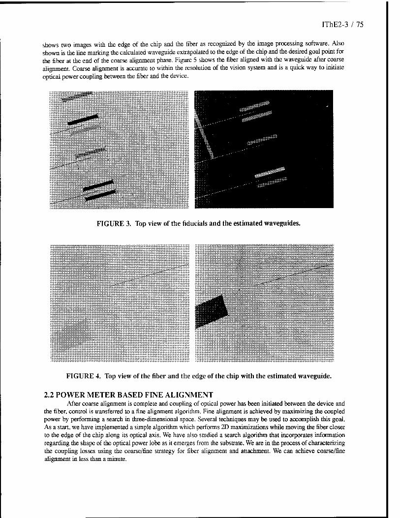
IThE2-3 / 75
shows two images with the edge of the chip and the fiber as recognized by the image processing software. Also shown is the line marking the calculated waveguide extrapolated to the edge of the chip and the desired goal point for the fiber at the end of the coarse alignment phase. Figure 5 shows the fiber aligned with the waveguide after coarse alignment. Coarse alignment is accurate to within the resolution of the vision system and is a quick way to initiate optical power coupling between the fiber and the device.
Ä ]'■:'■■&■':,'. '}.-:-■■- •''•... . ':::-.-. :
FIGURE 3. Top view of the fiducials and the estimated waveguides.
:™Av.*SSS*:*:::¥:»S :•'■:>>:::>:.X:Y*v,*'.*, :XK.:;:;:.:.';;7..;:; : YÄ. *:M.;«*«:«!
FIGURE 4. Top view of the fiber and the edge of the chip with the estimated waveguide.
2.2 POWER METER BASED FINE ALIGNMENT After coarse alignment is complete and coupling of optical power has been initiated between the device and
the fiber, control is transferred to a fine alignment algorithm. Fine alignment is achieved by maximizing the coupled power by performing a search in three-dimensional space. Several techniques may be used to accomplish this goal. As a start, we have implemented a simple algorithm which performs 2D maximizations while moving the fiber closer to the edge of the chip along its optical axis. We have also studied a search algorithm that incorporates information regarding the shape of the optical power lobe as it emerges from the substrate. We are in the process of characterizing the coupling losses using the coarse/fine strategy for fiber alignment and attachment. We can achieve coarse/fine alignment in less than a minute.
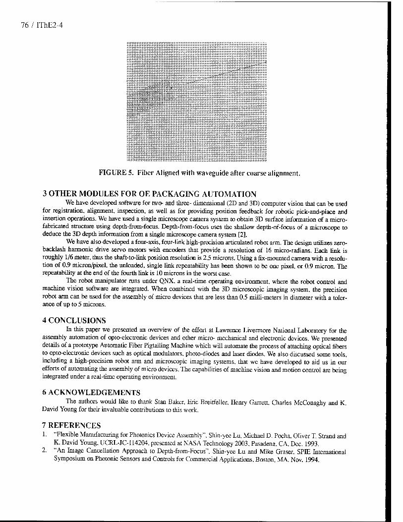
76 / IThE2-4
;:;:;:;£::x£:£xx
FIGURE 5. Fiber Aligned with waveguide after coarse alignment.
3 OTHER MODULES FOR OE PACKAGING AUTOMATION We have developed software for two- and three- dimensional (2D and 3D) computer vision that can be used
for registration, alignment, inspection, as well as for providing position feedback for robotic pick-and-place and insertion operations. We have used a single microscope camera system to obtain 3D surface information of a micro- fabricated structure using depth-from-focus. Depth-from-focus uses the shallow depth-of-focus of a microscope to deduce the 3D depth information from a single microscope camera system [2].
We have also developed a four-axis, four-link high-precision articulated robot arm. The design utilizes zero- backlash harmonic drive servo motors with encoders that provide a resolution of 16 micro-radians. Each link is roughly 1/6 meter, thus the shaft-to-link position resolution is 2.5 microns. Using a fix-mounted camera with a resolu- tion of 0.9 micron/pixel, the unloaded, single link repeatability has been shown to be one pixel, or 0.9 micron. The repeatability at the end of the fourth link is 10 microns in the worst case.
The robot manipulator runs under QNX, a real-time operating environment, where the robot control and machine vision software are integrated When combined with the 3D microscopic imaging system, the precision robot arm can be used for the assembly of micro devices that are less than 0.5 milli-meters in diameter with a toler- ance of up to 5 microns.
4 CONCLUSIONS In this paper we presented an overview of the effort at Lawrence Livermore National Laboratory for the
assembly automation of opto-electronic devices and other micro- mechanical and electronic devices. We presented details of a prototype Automatic Fiber Pigtailing Machine which will automate the process of attaching optical fibers to opto-electronic devices such as optical modulators, photo-diodes and laser diodes. We also discussed some tools, including a high-precision robot arm and microscopic imaging systems, that we have developed to aid us in our efforts of automating the assembly of micro devices. The capabilities of machine vision and motion control are being integrated under a real-time operating environment.
6 ACKNOWLEDGEMENTS The authors would like to thank Stan Baker. Eric Breitfeller, Henry Garrett, Charles McConaghy and K.
David Young for their invaluable contributions to this work.
7 REFERENCES 1. "Flexible Manufacturing for Photonics Device Assembly", Shin-yee Lu. Michael D. Pocha, Oliver T. Strand and
K. David Young, UCRL-JC-114204. presented at NASA Technology 2003, Pasadena. CA, Dec. 1993. 2. "An Image Cancellation Approach to Depth-from-Focus", Shin-yee Lu and Mike Graser, SPEE International
Symposium on Photonic Sensors and Controls for Commercial Applications, Boston, MA. Nov. 1994.
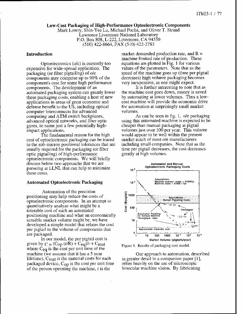
IThE3-l / 77
Low-Cost Packaging of High-Performance Optoelectronic Components Mark Lowry, Shin-Yee Lu, Michael Pocha, and Oliver T. Strand
Lawrence Livermore National Laboratory P.O. Box 808, L-222, Livermore, CA 94550
(510) 422-8664, FAX (510) 422-2783
Introduction
Optoelectronics (o/e) is currently too expensive for wide-spread application. The packaging (or fiber pigtailing) of o/e components may comprise up to 90% of the component's cost for some high performance components. The development of an automated packaging system can greatly lower these packaging costs, enabling a host of new applications in areas of great economic and defense benefit to the US, including optical computer interconnects for advanced computing and ATM switch backplanes, advanced optical networks, and fiber optic gyros, to name just a few potentially high- impact applications.
The fundamental reason for the high cost of optoelectronic packaging can be traced to the sub-micron positional tolerances that are usually required for the packaging (or fiber optic pigtailing) of high-performance optoelectronic components. We will briefly discuss below two approachs that we are pursuing at LLNL that can help to minimize these costs.
Automated Optoelectronic Packaging
Automation of the precision positioning may help reduce the costs of optoelectronic components. In an attempt to quantitatively analyze what might be a tolerable cost of such an automated positioning machine and what an economically sensible market volume might be, we have developed a simple model that relates the cost per pigtail to the volume of components that are packaged.
In our model, the per pigtail cost is given by c = (Cop (r/R) + Ceq)/r + Cmat where Ceq is the cost per unit time of the machine (we assume that it has a 5 year lifetime), Cmat is the material costs for each packaged device, C0p is the cost per unit time of the person operating the machine, r is the
market demanded production rate, and R = machine limited rate of production. These equations are plotted in Fig. 1 for various values of the parameters. Note that as the speed of the machine goes up (time per pigtail decreases) high volume packaging becomes very inexpensive, as one might expect.
It is further interesting to note that as the machine cost goes down, money is saved by automating at lower volumes. Thus a low- cost machine will provide the economic drive for automation at surprisingly small market volumes.
As can be seen in fig. 1, o/e packaging using this automated machine is expected to be cheaper than manual packaging at pigtail volumes just over 100 per year. This volume would appear to be well within the present market reach of most o/e manufacturers including small companies. Note that as the time per pigtail decreases, the cost decreases greatly at high volumes.
10;
10"
S 1000
g 100 o
Automated and Manual Optoelectronic Packaging Costs
10
1
Assumptions: Machine operator costs = $160K/yr Machine costs = $100K / 5yr
§\. Approximate V" Manual Pigtailing Costs
Approximate materials cost
1 10" 10 100 1000 10" 10s
Market Volume (pigtails/year)
Figure 1. Results of packaging cost model.
Our approach to automation, described in greater detail in a companion paper [1], relies heavily on the use of microscopic binocular machine vision. By fabricating
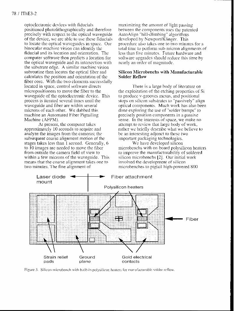
78 / IThE3-2
optoelectronic devices with fiducials positioned photolithographically and therefore precisely with respect to the optical waveguide of the device, we are able to use these fiducials to locate the optical waveguides in space. Our binocular machine vision can identify the fiducial and its location and orientation. The computer software then predicts a location for the optical waveguide and its intersection with the substrate edge. A similar machine vision subroutine then locates the optical fiber and calculates the position and orientation of the fiber core. With the two elements successfully located in space, control software directs micropositioners to move the fiber to the waveguide of the optoelectronic device. This process is iterated several times until the waveguide and fiber are within several microns of each other. We dubbed this machine an Automated Fiber Pigtailing Machine (AFPM).
At present, the computer takes approximately 10 seconds to acquire and analyze the images from the cameras; the subsequent coarse alignment motion of the stages takes less than 1 second. Generally, 6 to 10 images are needed to move the fiber from outside the camera field of view to within a few microns of the waveguide. This means that the coarse alignment takes one to two minutes. The fine alignment of
maximizing the amount of light passing between the components uses the patented AutoAlign "hill-climbing" algorithms developed by Newport/Klinger. This procedure also takes one to two minutes for a total time to perform sub-micron alignments of less than five minutes. Future hardware and software upgrades should reduce this time by nearly an order of magnitude.
Silicon Microbenchs with Manufacturable Solder Reflow
There is a large body of literature on the exploitation of the etching properties of Si to produce v-grooves mesas, and positional stops on silicon substrates to "passively" align optical components. Much work has also been done exploring the use of "solder bumps" to precisely position components in a passive sense. In the interests of space, we make no attempt to review that large body of work, rather we briefly describe what we believe to be an interesting adjunct to these two important packaging technologies.
We have developed silicon microbenchs with on-board polysilicon heaters to improve the manufacturability of soldered silicon microbenchs [2]. Our initial work involved the development of silicon microbenches to pigtail high-powered 800
Laser diode mount
Fiber attachment
Fiber
Strain relief pads
Ground plane
Gold electrical contacts
Figure 3. Silicon microbench with built-in polysilicon heaters for manufacturable solder reflow.

IThE3-3 / 79
nm laser diodes to single-mode fibers. The success of the prototype has led us to develop several new designs. For example, the microbench shown in figure 3 is for packaging a 1550 nm DFB laser. On the left side of the microbench, we photolitho- graphically pattern gold pads to provide a ground plane for the laser and stress relief for the wire bonds. To attach the fiber on the other side of the microbench, we build two heating elements of polysilicon which are attached to gold bonding pads for electrical contact. In the center of each heater, we pattern a gold pad on a layer of silicon dioxide. This gold pad provides the solder attachment base while the silicon dioxide electrically isolates the gold pad from the polysilicon heater. The gold pads are 1 mm by 0.5 mm each and are sufficiently large to solder upto a 250 micron diameter fiber at the two attachment pads. Presently, we use either 100-micron diameter solder balls or solder paste to attach the metalized fiber.
The performance of the polysilicon heaters on our prototype is very reproducible with a specially constructed power supply that allows us to accurately control the magnitude and time of the applied current. Fiber positioning is done by active alignment to sub-micrometer tolerances. We typically apply one amp of current for approximately 0.5 sec to reflow solder at the fiber attachment points. We observe no decrease in the light coupled from an 800 nm laser diode into a single-mode fiber before and after the solder reflow and cooling, and have achieved upto 65% optical coupling with conically tapered fibers
Our microbench geometries with on- board heaters allow rapid attachment of other components to be placed on the micro- bench as well. Applying larger currents for longer periods of time allows solder reflow at some distance from the heaters. Using solders with different melting temperatures and judiciously choosing the order of attachment allows a variety of components to be soldered to the microbench without movement of previously attached components. Generally, components furthest from a heater are attached first using a high current through the heater. We can solder a thermoelectric cooler, a thermistor,
and a laser diode onto our microbench at different distances from the heaters in less than 15 minutes. We envision that the placement and soldering of these components, which does not require sub- micron alignment, onto the microbenches could be performed by an automated system in only a few minutes. As the last step, the fiber must be aligned to sub-micron tolerances and is attached using the least current through the heaters.
The idea of on-board heaters lends itself to applications other than packaging laser diodes. We are presently designing a longer microbench with heaters at each end to pigtail both ends of a semiconductor optical amplifier.
Conclusions and Future Work
We have described some of the ongoing efforts at LLNL to reduce the costs of optoelectronic packaging. As a national laboratory, an increasingly significant portion of our mission is devoted to assisting US industry. We believe the efforts described here are important to the US optoelectronics industry and we are prepared to develop these technologies in partnership with US industry.
We have recently embarked on an ARPA funded program that will build on the automated packaging work described here. ARPA will fund LLNL, the MIT Manufacturing Institute, United Technologies Photonics, Ortel, and Newport-Klinger to develop a commercially available automated optoelectronic packaging machine. The partners in this effort will be reporting on our results in the near future.
References:
[1] Mark Lowry, Shin-Yee Lu, Deepak Sood, Oliver T. Strand, "Machine Vision and Motion Control Applied to the Packaging of Opto-Electronic Devices," elsewhere in this Digest
[2] A recent patent describes a similar device - Blonder & MacDonald, "Article that comprises a laser coupled to an optical fiber," U.S. Patent #5,307,434

80 / IThE4-l
Manufacturing Technology for Tactical Grade Fiber Optic Gyros
Persis A. Elwood Wright Laboratory
Manufacturing Technology Directorate WL/MTEC Bldg 653 2977 P St, Suite 6
Wright-Patterson AFB, OH 45433-7739
Phone: (513) 255-2461 Fax: (513) 476-4420
Background The assembly of fiber optic gyros (FOGs) is currently a very labor intensive and
expensive process which is driven by the extreme accuracy required in assembling the various components. Although the significant technology advantages of FOGs are very appealing, system insertion to date has been inhibited because of high cost. The Air Force awarded this four year program to Litton Systems, Inc., Guidance and Control Systems Division in September 1993 with an objective of reducing FOG cost to $1000/axis with a goal of $500/axis. The program is comprised of the following task areas: optical source, couplers, integrated optic chips (IOC), optical fiber, sensing coil, assembly and test.
Program Methodology The program includes two main thrusts to enable cost reduction. The first is to foster a
robust FOG industrial base by establishing a teaming arrangement between Litton and the component, material and equipment suppliers. Most of the direct FOG costs are ultimately due to labor - primarily from material and/or component suppliers. Without ManTech investment, suppliers tend to automate or improve processes based on payback analysis and profit generation. For defense related efforts this will not occur rapidly, if at all. As a result, product maturation and learning curves move out, and early FOG costs will be 10-20 times higher than mature FOG costs. In addition, by funding work at the vendor/supplier level (vs. the gyro integrator level) the program will be of benefit to more than just one FOG manufacturing house.
The second thrust area is variability reduction. Litton and team members must be able to demonstrate process capability as measured by process control indices (Cp and Cpk) which must be 1.33 or higher for key processes. The manufacturing process improvement tools which will be used on the program are Quality Function Deployment (QFD), Design of Experiments (DOE) and Statistical Process Control (SPC). QFDs translate customer requirements into critical processes and critical process parameters. DOEs are used to improve processes by determining the critical relationships between process steps and performance characteristics. SPC is used to monitor progress and control the process improvements. The variability reduction efforts will occur in conjunction with semi-automation of processes as well as the establishment of in-situ test.
The team members are: EG&G Optoelectronics (Super Luminescent Diode (SLD) light source), Hewlett-Packard (laser diode light source), Marlow Industries (Thermoelectric Cooler-TEC), IPITEK (couplers), Newport (IOC), PPO (IOC), 3M (optical fiber), and Optelecom (sensing coil). In addition, Litton is developing an automatic optical assembly station and a bulk fiber transfer winder.
Technical Effort The program consists of three phases. Phase I, a six month planning phase, has been
completed. Phase II is a 24 month implementation phase, which concludes with an intermediate production run of 30 gyros, built incorporating the initial manufacturing enhancements developed under the program. Phase III, 18 months, is the process verification phase and includes a production demonstration of 30 gyros and 5 IMUs (Inertial Measurement Units -

IThE4-2 / 81
there are three FOGs in each IMU). Qualification of Vendors will be part of this final build, and there will be independent test and evaluation of program results.
A key element in developing the Program Plan during Phase I was a survey of FOG manufacturers. This survey was used to form the requirements given to the component suppliers. They also ensured that the ManTech program would be supporting as much of the FOG community as possible.
The cost model developed for the program utilizes two optical configurations: a single axis configuration, and a triax configuration where one light source powers all three gyros of an IMU (Figure 1). The cost model assumes that a proven optical configuration is used and that on going cost improvements (non-ManTech) are pursued in parallel. The model also assumes 6000 FOG IMUs/year, and costs are in 1993 dollars. Where appropriate, commercial applications are considered. FOG component costs are shown in Table 1, and the cost model for an SLD triax configuration is shown in Table 2.
An Industrial Review Board (IRB) comprised of FOG IMU houses and component suppliers was also established during Phase I. The IRB meets every six months and its purpose is two-fold: to disseminate ManTech program information to the technical community as quickly as possible, and also to provide input and advise the Litton team where and when appropriate.
During Phase II the bulk of the variability reduction efforts takes place. Litton and the supplier team will be working to control both process and product variability while at the same time developing automated and semi-automated processes for various tasks to establish well understood and controlled manufacturing lines to effect the required cost reductions. The major task areas are summarized below:
Light Source - EG&G is the SLD supplier. Tasks include pigtailing and packaging optimization as well as test/screening. Hewlett Packard is the laser diode supplier. Tasks include fiber lens optimization, assembly and packaging improvements. Marlow is the TEC supplier. Tasks include auto sorting and loading of TEC elements, solder reflow improvements and test optimization.
Couplers - IPITEK - Effort will focus on automatic fiber preparation, packaging optimization, and a computer controlled fabrication process.
Optical Fiber - 3M - Tasks include yield improvement, test optimization and fiber/preform quantity.
Sensing Coil - Optelecom - Coil winder design optimization and wound coil robustness characterization data are the tasks.
Auto Optical Assembly, IOC, and Bulk Winder - Litton/Newport/PPO - The auto optical assembly task includes station design, process optimization and validation. The IOC task includes low cost package design and upgraded alignment stages. The bulk winder task includes station design and process validation.
The team will then demonstrate the ManTech process improvements with an intermediate production run and test of 30 gyros at the end of Phase II.
After the results of the Phase II build have been analyzed and appropriate process improvements incorporated into the manufacturing processes, a final production run of 30 gyros and 5 IMUs will take place during Phase III. These gyros and IMUs will be tested at a government test facility (Central Inertial Guidance Test Facility - CIGTF). Phase III also allows an opportunity for a separate funded technology transfer activity to take place after the build and vendor qualification.
Summary Phase I was completed successfully and Phase II started in May 1994. The Phase II build is scheduled for July 1995. Litton and the subcontractors are all on schedule and well on the way to meeting the program cost objectives and establishing an enhanced, flexible industrial base.
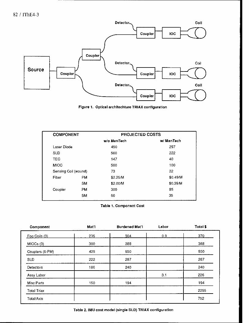
82 / IThE4-3
Detector, Coil
Figure 1. Optical archltechture TRIAX configuration
COMPONENT PROJECTED COSTS
w/o ManTech w/ ManTech
Laser Diode 450 297
SLD 500 222
TEC 147 40
MIOC 500 100
Sensing Coil (wound) 73 22
Fiber PM $2.25/M $0.49/M
SM $2.00/M $0.39/M
Coupler PM 300 85
SM 60 35
Table 1. Component Cost
Component Mat'l Burdened Mat'l Labor Total $
Foa Coils (3) 235 304 0.9 370
MIOCs (3) 300 388 388
Couplers (5-PM) 425 550 550
SLD 222 287 287
Detectors 186 240 240
Assy Labor 3.1 226
Misc Parts 150 194 194
Total Triax 2255
Total/Axis 752
Table 2. IMU cost model (single SLD) TRIAX configuration
Thursday, February 23, 1995
Time-Domain Simulations
IThF 3:30 pm-5:00 pm Salon 4
Reinhold Pregla, Presider Fern Universität, Germany
84 / IThFl-1
NUMERICAL SIMULATIONS OF LIGHT BULLETS, USING THE FULL VECTOR, TIME DEPENDENT, NONLINEAR MAXWELL EQUATIONS
Peter M. Goorjian Mail Stop T27B-1
NASA Ames Research Center Moffett Field, CA 94035-1000
(415) 604-5547 FAX (415) 604-1095
Yaron Silberberg Dept. of Physics of Complex Systems The Weizmann Institute of Science
76100 Rehovot, Israel 972-8-342034
FAX 972-8-344109
I. Introduction
From the exact Maxwell's equations, solutions have been obtained that are similar to light bullets [1], i.e. optical pulses that are self-supporting under the effects of diffraction, anomalous dispersion and nonlinear refraction. These pulses propagate stably, without any essential changes in shape or spectral content. For comparison, standard theory, which uses the nonlinear Schrodinger equation (NLSE), (an approximation to Maxwell's equations), predicts [1] that under the effects of nonlinear refraction, self-focusing will lead to the collapse of optical pulses. Also, additional calculations show that when two of these pulses are counter- propagating, upon interacting, they change each others' trajectories. These pulses are extremely small, approximately 25 fs in duration and contain about 5 wavelengths.
The solutions are computed by solving the time dependent, vector, nonlinear Maxwell's equations in two space dimensions [2-5]. The linear dispersion is modeled by a Lorentzian model with a single resonance and the nonlinear refraction is modeled by a Kerr-like instantaneous nonlinearity. The optical carrier is retained in the calculations so that each wavelength in the pulse is resolved. Also, since the Maxwell's equations are solved exactly, all higher order effects, such as higher order dispersion, are automatically accounted for in these simulations.
For comparison, standard methods of analysis and numerical simulation use the NLSE. That ap- proach solves only for the envelope of the pulse. It assumes that the envelope is slowly-varying and that it contains one hundred to one thousand wavelengths [6]. Also, additional terms must be added to the NLSE to account for higher order effects [7]. Hence the NLSE cannot be used for the simulation of the small pulses in this study. Its approximations may account for its inability to predict stable light bullets.
The numerical algorithm employed in this paper is described in Refs. 2-5. It was used for calculations of propagating and interacting temporal [2-3,5] and spatial [4,5] solitons. In those simulations, the nonlinear effects included Kerr-like instantaneous as well as Raman dispersive nonlinearities. Convolution integrals described the linear and nonlinear dispersive effects. Their evolution was determined by a coupled system of nonlinear, ordinary differential equations. These equations were nonlinearly coupled to Maxwell's equations through the electromagnetic field. This entire system of equations was solved by a finite-difference algorithm, as described in Ref. 3. With that development, it became possible, for the first time, to solve the nonlinear, vector Maxwell's equations exactly, without having to go use approximations such as the NLSE. In this paper, that algorithm is used under the simplification that the nonlinearity is entirely instantaneous.
In order to isolate each material effect on the optical wave, the sequence of calculations were done methodically. In the first calculation, only dispersion acted on a pulsed plane wave. Next diffractive effects on a beam were calculated. These two effects were then allowed to act together on a pulse. Next nonlinear refraction was introduced as the third effect, with the result that a stable self-supporting pulse was created. Finally, two of these pulses interacted, while counter-propagating, and they deflected each other.
II. Results
The results are shown by displaying the variation of the electric field in the computational domain. The computational domain is 62 ^m along the direction of propagation and 21 /zm in the transverse direction.
Figure 1 shows the results of dispersion on a pulsed plane wave at four instants of time in its propagation. The source is turned on at the left side of the domain. The results are shown in a window in the computational domain that is centered in the transverse direction and that is 13 fim wide. The dispersion
IThFl-2 / 85
in the material is characterized by a single Lorentzian resonance and is described by the following first order susceptibility function: x(1)(") = (wj^e, - Coo))/(w^ - w2). Here e«, = 9,e, = 21 and wr = 6.0 x 10¹⁴
rad/sec. The wave length of the plane wave is A = 1.55/im (in vacuum), with v = 1.94 x 10¹⁴ Hz or u = 1.22 x 10¹⁵ rad/sec, which is in the anomalous dispersion range. The electric field strength is 2.9 x 10¹⁰
Volts/m. The pulse has a hyperbolic secant envelope with a characteristic decay time constant of 10.3 fs. Notice that as the wave propagates, the pulse lengthens due to dispersion. Each band represents one wavelength.
Figure 2 shows the results of diffraction of a beam. Again the source is turned on at the left side and the four plots show the progression of the beam, including the beam's front edge. The cross sectional profile of the beam source is a hyperbolic secant envelope with a characteristic length of 0.517 /im, which is one wavelength of the optical carrier in a dielectric with an index of refraction equal to three. As the beam propagates, it widens due to diffraction.
Figure 3 shows the effects of both dispersion and diffraction acting on a pulse. The parameters of dispersion and diffraction are those from the previous two calculations. The plot at each time step is scaled by the maximum and minimum values of the electric field at that instant, rather than using global values, which would wash out the pulse's appearance at the later times due to its diminishing amplitude. Notice that the spreading rates of the pulse due to dispersion and diffraction are approximately equal. Also the individual wavelengths are clearly discernible and there are additional wave patterns in the pulse.
Figure 4 shows the pulse propagating under the combined effects of anomalous dispersion, diffraction and nonlinear refraction. The strength of the nonlinearity is given by the nonlinear index coefficient n\ = 3.2 x 10~20 m2/W, (characteristic of silica at A = 1.55 /im). Here the length of the computational domain has been reduced to 47 /im from 62 /im, since the longer length is no longer needed. Notice that the pulse is now self-supporting, without any essential changes in size or shape. The wavelengths are distinguishable and there are about five wavelengths in the pulse. Around the core of the pulse, which supports itself, is a surrounding low level outer coat, which disperses and diffracts away from the core.
Figure 5 shows a plot of the electric field values along the centerline of the computational domain at the four times shown in the previous figure. Again this figure shows that the essential shape of the pulse is maintained. Figure 6 shows the temporal power spectrum of the pulse at four locations along the centerline. Here the peak of the spectrum remains essentially unchanged. Hence, the results in Figs. 4-6 show that the pulse is essentially self-supporting and stable, viz. similar to a light bullet. Also, calculations were performed in which the pulse traveled twice the distance shown in Fig. 4 and the pulse maintained its support.
Figure 7 shows that when two of these pulses are counter-propagating, upon interacting, they change each others' trajectories. Initially, the right pulse is slightly upward in comparison to the left pulse. At the third instant plotted, the pulses have just passed each other and the initially higher pulse is still slightly higher. By the four instant, the plot shows that the two pulses have become aligned vertically. Although the effect is small, it shows that one of these light bullet like pulses can alter the path of another through an interaction.
The calculations were performed on a Cray C-90 computer and took 180 seconds per case, relatively minor calculations. The first author thanks Allen Taflove of Northwestern University for many helpful discussions.
III. References
1. Y. Silberberg, Opt. Lett. , 15, No. 22, 1282-1284 (1990).
2. P. M. Goorjian and A. Taflove, Opt. Lett. , 17, No. 3, 180-183 (1992).
3. P. M. Goorjian, A. Taflove, R. M. Joseph and S. C. Hagness, IEEE J. Quantum Electronics , 28, 2416-2422 (1992).
4. P. M. Goorjian, A. Taflove and R. M. Joseph, OSA Proceedings , 17, Short Wavelength V: Physics with Intense Laser Pulses, 66-69, (March 1993).
5. P. M. Goorjian, A. Taflove and R. M. Joseph, Nonlinear Guided-Wave Phenomena, OSA and IEEE/LEOS, Cambridge, England, Sept. 19-22, 1993.
6. G. G. Luther, A. C. Newell and J. V. Moloney, to appear in Physica D (1994).
7. G. P. Agrawal and C. Headley, Phys. Rev. A, 46, No. 3, 1573-1577 (1992).
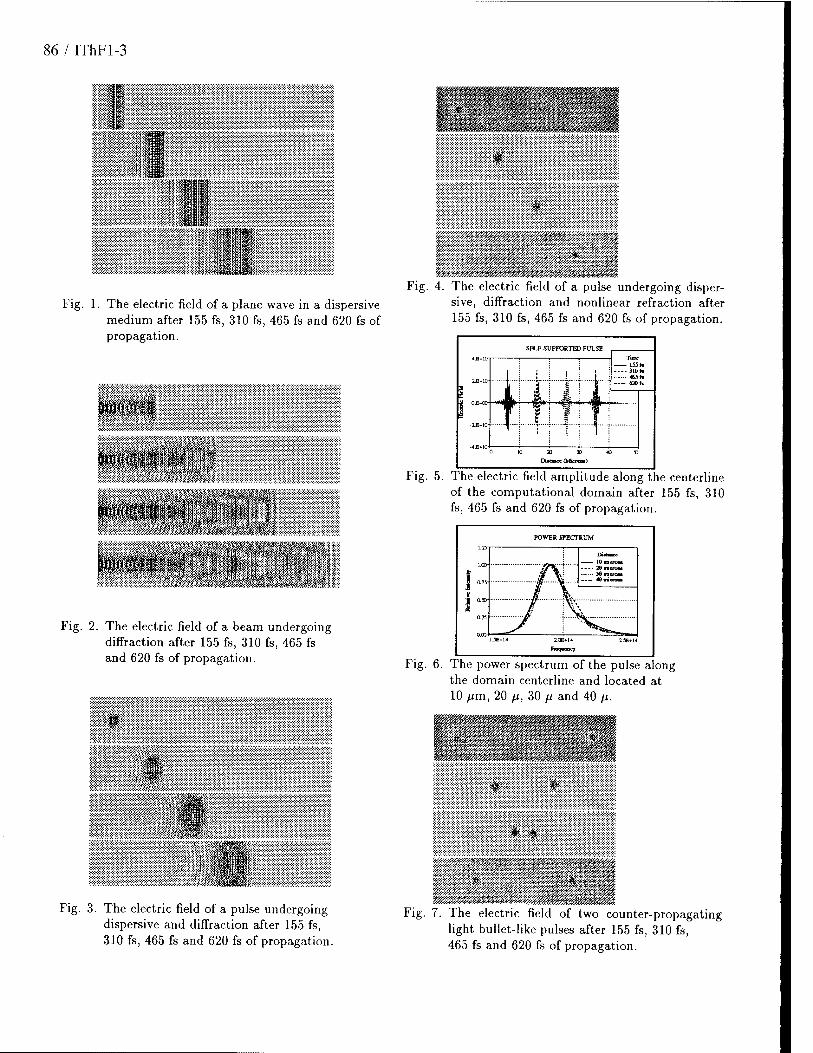
86 / IThFl-3
Fig. 1. The electric field of a plane wave in a dispersive medium after 155 fs, 310 fs, 465 fs and 620 fs of propagation.
■ •:.<■.••-. =:^^i
Fig. 4. The electric field of a pulse undergoing disper- sive, diffraction and nonlinear refraction after 155 fs, 310 fs, 465 fs and 620 fs of propagation.
Fig. 2. The electric field of a beam undergoing diffraction after 155 fs, 310 fs, 465 fs and 620 fs of propagation.
Fig. 3. The electric field of a pulse undergoing dispersive and diffraction after 155 fs, 310 fs, 465 fs and 620 fs of propagation.
SELF-SUPPORTED PULSE
DUanee (&&rew)
Fig. 5. The electric field amplitude along the centerline of the computational domain after 155 fs, 310 fs, 465 fs and 620 fs of propagation.
POWER SPECTRUM
a
Dinare lOnffi« Wwiaxxm Uno« «nm» *# V ■
ß Ik F : V* \
Fig. 6. The power spectrum of the pulse along the domain centerline and located at 10 /zm, 20 (i, 30 fi and 40 /z.
* ♦!
Fig. 7. The electric field of two counter-propagating light bullet-like pulses after 155 fs, 310 fs, 465 fs and 620 fs of propagation.

IThF2-l / 87
Finite-Difference Time-Domain (FDTD) Analysis of Nonlinear Optical Waveguiding Devices: N. Ackerley, S.K. Chaudhuri, Dept. of Electrical and Computer Engineering, University of Waterloo, Waterloo, Ontario, Canada N2L 3G1 FAX # (519) 746-3077
Introduction
In this work we have developed the theory required for a nonlinear FDTD simulator, including the propagator, the implementation of the nonlinearity, boundary and stability conditions, and source gen- eration. We validated the simulator by reproducing the published results for a self-guiding structure [1] and for a nonlinear directional coupler [2]. We then demonstrate the operation of a rudimentary soliton coupler.
Implementation of Nonlinearity
Third order nonlinear effects can be modelled effectively using the FDTD formulation [3]. In this paper, we study structures containing Kerr-law media, as well as two kinds of saturable media. Fol- lowing [4], the forms of nonlinear permittivity n2=n^+f(a | e p) for the three cases are:
/© = % ; Kerr-law (1)
/ß) = £/(l+£/A«2t) ; Saturable,two-level (2)
/(£) = A«^t[l-exp(-^/A«,2J] ; exponential saturation (3)
The saturable permittivity have been defined in such a way that they reduce to the Kerr-law case for small fields. Real materials exist which have both self-focusing (a > 0) and self-defocusing (a < 0) nonlin- earities and they tend to saturate at permittivities a few percent different from their no-field values. The coefficient of nonlinearity a is generally many orders of magnitude less than unity, but since it scales with power, it has been chosen unity throughout this work for convenience.
The non-linearity can be incorporated into the FDTD analysis in two ways. If the features being studied involve only the field patterns at steady-state, then the nonlinearity can be incorporated in a straight for- ward manner. Assuming the magnitude of the electric field is changing very slowly, it (e"+1) can be approximated using the values of the fields at the two time-steps previous (e", e""1) to the current one using:
i "i|2 - (e""1)2-2e'-1e"cos(£0AT) + (£'f I £ I — . 2 , . > VV
sin k0Ax
where A^ is the free-space propagation factor and Ax is the time-step in the FDTD implementation. The modified propagator makes use of this equation to define the local index of refraction at each time step in the FDTD simulation. Using this method the turn-on time of the nonlinearity is l.5Ax/c; this is acceptable for many applications. Alternatively, one can attempt to reduce the delay in the turn-on of the nonlinearity by rewriting (4) such that the field magnitude at the current time step is calculated in terms of the field at the current and pre- vious time steps. This eliminates a delay of AT/C in the turn-on of the nonlinearity, so that the resulting dispersion is no more than the usual FDTD numerical dispersion. For the Kerr-law this results in a cubic equation for the electric field calculations in the propagator, which is time consuming to solve exactly. However, using just a few iteration of a root-finding algorithm (we used a bisection procedure combined with quadratic inverse interpolation), the response-time of the non- linearity can be improved immensely. Furthermore, approximating the solution in this way is easily adapted to saturable nonlinearities.

88 / IThF2-2
Numerical Results
Three simulations were carried out using the nonlinear FDTD propagator described earlier; a simple self guiding structure, a nonlinear directional coupler, and a soliton coupler.
The self-focussing waveguide was used as a validation test of the simulator. As shown in Fig.1, it consists of a layer of exponentially saturating dielectric (£2 = 2.215, oc=i, A«s
2at = 0.3, d^ = X = \\m)
sandwiched between linear media fo = e3 = 2.25). Note that for low fields, the core index is lower than that of the cladding, and the structure does not guide radiation; this structure constitutes a waveguide only in the presence of large electric fields.
First, the effective indices and field profiles were determined for numerous power levels. As shown in Fig.2 this is in excellent agreement with [1]. However, there are two regimes of operation: one where the effective index increases, and another where it decreases with power. We were able to repro- duce the former, including cut off power of 2.2 nw/m, but not the latter. It is believed that the part of the curve with very low effective indices represents unstable solutions to the nonlinear Helmholtz equation. Unfortunately, in [1] authors do not specify by what method they obtained their solutions, except mentioning that it was a numerical method.
Next, for several power levels, the field profiles from finite-differencing were used as FDTD sources. It was found that the field patterns remained constant with propagation distance, and were absorbed very effectively by the dispersive boundary conditions (DBC). If the power level was increased while keeping the profile the same, then the beam would become slightly more focussed with propagation distance, while radiating off a small amount of power. If the power level was decreased for the same profile, then the beam would defocus and become entirely radiative if the power was below threshold. These are same phenomena as observed qualitatively in [1]. These results validates the nonlinear FDTD.
Next, the simulator was used to study a nonlinear directional coupler. The results are in excellent agreement with [2]; as the power increases coupling becomes less, and once the critical power is sur- passed, the complete power transfer no longer occurs. One difference is that, at very high powers, we observed less power transfer than is seen in [3]. This may be because the coupled mode theory assumes that the field profile does not change with power; in fact, the field profile does change, and FDTD models it correctly.
Finally, the soliton coupling has been demonstrated using the FDTD simulator. In comparison with the nonlinear directional coupler, the threshold power is about five times higher than a coupler made from the same materials, but the switching is much more abrupt.
In conclusion, we expect the nonlinear FDTD simulator developed here to be most useful when very specific results need to be verified, or when the structure being studied cannot be analyzed by other methods.
References
[1] H.A. Jamid, S.J. Al-Bader; "Electronics Letters, Vol.29, No.1, pp.83-84, 1993
[2] G.I. Stegeman, E.M. Wright; "Optical and Quantum Electronics", Vol.22, No.1, pp.95-122,1990
[3] ST. Chu, W.P. Huang, S.K. Chaudhuri; "Computer Physics Communications", Vol.68, pp.451- 484,1991
[4] R.A. Sammut, C. Pask; Journal of Optical Society of America, Part B, Vol.8, No.2, pp.395-402, 1991

IThF2-3 / 89
third order ABC
ü m Q
M V
M o
jefiected'ltotal ^ .,_. _„_,,
Se&on^pregion jW:;?':';*■;
Ü ffl Q
hi u M O
Z,J
third order ABC source plane (i = i.)
Fig. 1. Self-guiding Nonlinear Waveguide
2.5
£ 2
eu 1.5
O o, i
0.5 from Jamid [lj finite-difference solution x
1.5 1.505 1.51 1.515 1.52 effective index, ne
Fig. 2. Dispersion Graph for Self-guiding Nonlinear Waveguide
1.525 1.53

90 / IThF3-l
Time Domain Analysis of Nonlinear Optical Waveguides
D. Schulz, M. Pohl, E. Voges Lehrstuhl für Hochfrequenztechnik, Universität Dortmund
D-44227 Dortmund, Germany Phone: +49 231 755-2489; Fax: +49 231 755-4631
I. Introduction In general coupled-mode theories provide a good insight on nonlinear devices. However, they are unreliable for the analysis of the detailed behaviour and quantitative predictions. Therefore numerical methods are necessary [1]. In nonlinear waveguides the orthogonality relation between modal fields does not hold. Therefore, optical pulses cannot be expanded into harmonic waves, and the application of beam propagation techniques [2-6] is questionable. On the other hand, time domain propagation algorithms allow to simulate the propagation of pulses [7] and have the general advantages of full vectorial formulation, calculation of transmission characteristica in one step, and the automatic and accurate inclusion of reflections. Yee's algorithm described in [7] has been extensively used in microwave techniques and was introduced in integrated optics by [8]. This algorithm has been extended to the analysis of nonlinear waveguides [9-12]. One significant disadvantage restricts the application of this method. That is, a stability condition has not yet been derived for the analysis of nonlinear waveguides. In this paper, we present an unconditionally stable method which allows the analysis of nonlinear waveguides.
II. Theory The propagation within the time domain is described by Maxwell's curl equations. Neglecting dispersion effects, considering a Kerr medium and TEM-waves, a nonlinear relative dielectric constant srej is introduced with
srel = n2(z) + 3noX(3)(z)E2 . (1)
Here, n^(z) represents the axial variation of the index distribution and x (z) describes the
nonlinearity of the medium. In a first step srel is assumed to be constant, because actually the known initial field Ey is inserted. The FDTD method is formulated by discretizing Maxwell's curl equations over a finite volume and approximating the derivatives with centered difference approximations. Therefore the discretization in space coincides with Yee's algorithm. In contrast to Yee's algorithm all field vectors are determined at the same time step. The discretization in space and time are indicated by the index v and k, respectively. Stability problems can be avoided, if the field values are approximated by the averaged field values at time steps k and k+1. Hence, with the central difference approximation we have
Fk+1 — Fk 1 k+0.5 -^y.v -^y.v _ l (vik+] - Rk+1 4- FTk - FTk )
brel,v . . ,_, . lnx,v+0.5 "-x.v-O.S "l~ nx,v+0.5 nx,v-05/ At 2c0Az TTK + i _ TJK
•"■x.v+o.s -"-x.v+o.s
At 2c0 Az
• (2) (Fk+l _ pk+1 + Fk -Fk )
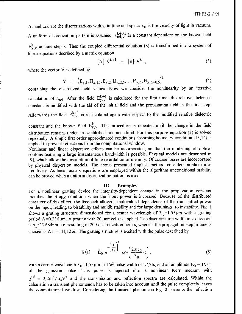
IThF3-2 / 91
At and Az are the discretizations widths in time and space. c0 is the velocity of light in vacuum.
A uniform discretization pattern is assumed. eke| y
5 is a constant dependent on the known field
Ek v at time step k. Then the coupled differential equation (8) is transformed into a system of
linear equations decribed by a matrix equation
[A]-Vk+1 = [B]-Vk , (3)
where the vector V is defined by \ T
V = (Ey i,Hxl5,Ey2,HX2.5,"-,Eyn,Hxn+o.5) . (4)
containing the discretized field values. Now we consider the nonlinearity by an iterative
calculation of srel. After the field Ey^1 is calculated for the first time, the relative dielectric
constant is modified with the aid of the initial field and the propagating field in the first step.
Afterwards the field Ey*1 is recalculated again with respect to the modified relative dielectric
constant and the known field Ek v. This procedure is repeated until the change in the field
distribution remains under an established tolerance limit. For this purpose equation (3) is solved repeatedly. A simple first order approximated continuous absorbing boundary condition [13,14] is applied to prevent reflections from the computational window. Nonlinear and linear dispersive effects can be incorporated, so that the modelling of optical solitons featuring a large instantaneous bandwidth is possible. Physical models are described in [9], which allow the description of time retardation or memory. Of course losses are incorporated by physical dispersion models. The above presented implicit method considers nonlinearities iteratively. As linear matrix equations are employed within the algorithm unconditional stability can be proved when a uniform discretization pattern is used.
ED. Examples For a nonlinear grating device the intensity-dependent change in the propagation constant modifies the Bragg condition when the input power is increased. Because of the distributed character of this effect, the feedback allows a multivalued dependence of the transmitted power on the input, leading to bistability and multibistability and for large detunings, to instability. Fig. 1 shows a grating structure dimensioned for a center wavelength of A,0=155|j,m with a grating period A=0.236um. A grating with 20 unit cells is applied. The discretization width in z-direction is hz=23.684nm, i.e. resulting in 200 discretization points, whereas the propagation step in time is
chosen as At = 41,12 as. The grating structure is excited with the pulse described by
't^2
E(t) = E0-e ^ -cos f2KC0 ^
X, 0 (5)
with a carrier wavelength A,0=l,55u,m, a l/e2-pulse width of 27,3fs, and an amplitude E0 = lV/m of the gaussian pulse. This pulse is injected into a nonlinear Kerr medium with
X(3) = 0,2m2/(j,0V2 and the transmission and reflection spectra are calculated. Within the
calculation a transient phenomenon has to be taken into account until the pulse completely leaves the computational window. Considering the transient phenomena Fig. 2 presents the reflection
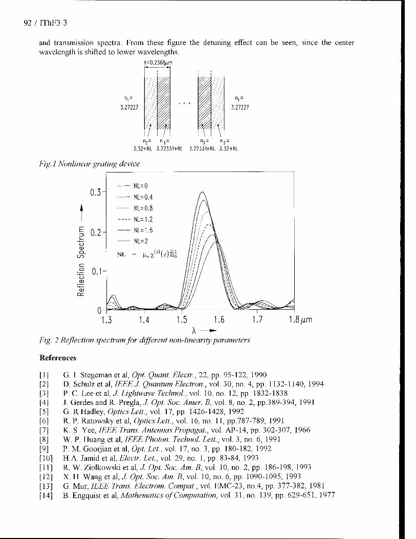
92 / IThF3-3
and transmission spectra. From these figure the detuning effect can be seen, since the center wavelength is shifted to lower wavelengths.
A=0.2368,um
3.27227
n,=
3.27227
"2" '3- 3.32+NL 3.22331+NL 3.22331+NL 3.32+NL
Fig. 1 Nonlinear grating device
.8/xm
Fig. 2 Reflection spectrum for different non-linearity parameters
References
[I] G. I. Stegeman et al, Opt. Quant. Electr., 22, pp. 95-122, 1990 [2] D. Schulz et al, IEEEJ. Quantum Electron., vol. 30, no. 4, pp. 1132-1140, 1994 [3] P. C. Lee et al, J. Lightwave Technol, vol. 10, no. 12, pp. 1832-1838 [4] J. Gerdes and R. Pregla, J. Opt. Soc. Amer. B, vol. 8, no. 2, pp.389-394, 1991 [5] G. RHadley, Optics Lett., vol. 17, pp. 1426-1428, 1992 [6] R. P. Ratowsky et al, Optics Lett., vol. 16, no. 11, pp.787-789, 1991 [7] K. S. Yee, IEEE Trans. Antennas Propagat, vol. AP-14, pp. 302-307, 1966 [8] W. P. Huang et al, IEEE Photon. Technol. Lett, vol. 3, no. 6, 1991 [9] P. M. Goorjian et al, Opt. Let., vol. 17, no. 3, pp. 180-182, 1992 [10] H.A. Jamid et al, Electr. Let, vol. 29, no. 1, pp. 83-84, 1993 [II] R. W. Ziolkowski et al, J. Opt. Soc. Am. B, vol. 10, no. 2, pp. 186-198, 1993 [12] X. H. Wang et al, J. Opt Soc. Am. B, vol. 10, no. 6, pp. 1090-1095, 1993 [13] G. Mur, IEEE Trans. Electrom. Compat., vol. EMC-23, no.4, pp. 377-382, 1981 [14] B. Engquist et al, Mathematics of Computation, vol. 31, no. 139, pp. 629-651, 1977
IThF4-l / 93
FDTD Modeling of Nonperfectly Conducting Metallic Thin Film Gratings
Justin B. Judkins and Richard W. Ziolkowski Electromagnetics Laboratory
Department of Electrical and Computer Engineering
The University of Arizona
Tucson, AZ 85721 USA
Electromagnetic fields in and near metallic corrugated surfaces can be numerically modeled by a variety
of methods with different degrees of completeness and complexity. The finite difference-time domain (FDTD)
technique is a good modeling approach to this problem because the full vector Maxwell's equations are solved
directly on a mesh that coincides with the specified problem geometry. In order to consider more closely
the situation where an optically thin layer of a metal such as gold has been applied to the surface of the
grating, we have added several enhancements1'2 to the standard FDTD approach3'4. For the conductor
region, we employ the time domain Lorentz equation to obtain the complex refractive index. This is an
improvement to the standard a model because many metals at optical frequencies have a greater imaginary
than real component in their refractive indices. We sample the fields scattered by the grating along a plane
within the computational grid and use a far field transform to obtain the radiation pattern at some large
distance away from the grating. Finally, to drive the source into the problem, an aperture beam focused
onto the surface of the grating, we have constructed a total field/scattered field boundary which is designed
to propagate an incident Gaussian beam field towards the grating while still allowing the scattered field to
propagate without distortion away from the grating. This FDTD simulator can be applied to any beam and
grating configuration, such as oblique incidence of a finite beam onto a uniform grating that generates only
one diffraction order or normal incidence of a beam onto a grating with parabolic variation in the depths of
grooves. The later configuration includes the case where the grating is a finite Fresnel grating that spans
several wavelengths and is designed to focus the incident beam to a point near the grating.
For the noble metals (Ag, Au, and Cu), and also for the metal Al, the complex refractive indices at
optical frequencies are more imaginary than real (For instance, the refractive index of gold at A = .78 pm
is n — 0.175 — J4.91). In order to apply this refractive index to a material, we include an additional model
for the electric polarization, P, in the FDTD algorithm and solve it simultaneously with the fields. FDTD
models using only a phenomenological <r term to represent conductivity in Maxwell's equations can provide
a complex angle for the refractive index that is strictly less than T/4. On the other hand, the Lorentz model
of the metal allows the refractive index arguments to be greater than 7r/4, and gives the correct reflection
coefficient, as confirmed with several validation problems, at these metal interfaces. Moreover, since the field
is not completely canceled at the surface of a realistic conductor, a perfect conductor model (Etan = 0) is a
poor description of the material.
The time domain Lorentz model is
dt2 + dt 2 PL + T - PL +LOI PL = eoxoul E
where the three Lorentz parameters (xo, wo, T) and a forth parameter, the instantaneous responce of the
medium e^, are chosen to give the correct complex refractive index at one desired frequency. Because only
two degrees of freedom are required to fit the model to a refractive index, two of the parameters, xo and
94 / IThF4-2
foo, must initially be chosen. The remaining parameters, w0 and T, are then determined from the frequency
domain Lorentz model
n2(w) = bE. + uoXo fO >uJ% - w2 + juT
We have simulated an incident beam (A = .78 pm) focused onto a grating with a gold layer and onto
a perfectly conducting grating and compared the scattering efficiencies of the blazed beam for these two
configurations as the size of the grooves are increased while the period of the grating remains constant. The
zeroth order (reflection) and first order scattering angles are measured in the far field. A differential signal
S = (öi - D2)/{Di + D2) is calculated from their respective intensities, Di and D2. For the cases shown
in Figs la and lb we have specified the depth of the grooves, h, as h = 0.50 pm for the TE polarization and
h = 0.39 pm for the TM polarization. These values of h were chosen to optimize the conversion between the
m — 0 and m = 1 beams for each polarization.
The TE case is shown in Fig la. The behavior of S for the Au layer grating is similar to the p.e.c.
grating but we see that a shift occurs in the relative teeth-to-groove size which optimizes the coupling for each
grating. The change in sign of S occurs when the efficiency of the first order scattered beam is increased due
to energy being coupled into the grooves. The grooves in the grating act like terminated parallel waveguides,
returning the incident energy with magnitude and phase that depends on the width and depth of the groove.
Below the cutoff size there is little variation in the phase of the returned beam. As the size of the groove
increases from its cutoff value, the phase shift increases. When the scattered wave undergoes a w phase
shift, the m = 1 beam is produced more efficiently so S becomes negative. A further increase in the groove
width leads to a 2ir phase shift, and the grating produces the m = 0 beam so S becomes positive again.
Because the cutoff size and propagation values for the waveguide-like structure are dependent partially on
the material in the walls of the structure, the signal S for the Au film grating is shifted from that of the
perfect conductor grating. In the corresponding TM case shown in Fig lb, cutoff in the grooves is not a
factor in determining the amount of energy coupled into the grating. For this case the change in S resulting
from the use of a realistic, rather than perfect, conducting layer is only attributed to a variation in the
impedance of the grating due to the materials.
A grating, used as a diffractive optic element, can be designed to focus an incident beam by varying the
depth of the grooves as a quadratic function. The phase shift of the reflected beam along its cross section is
determined not only by the individual groove depths but also by the properties of the walls of the groove,
especially when the size of the groove is close to the cutoff size. We have constructed this Fresnel lens and
have driven the problem with a TE polarized incident beam at normal incidence. The beam spot size is
made large enough to completely illuminate the entire grooved region. Four test cases were studied with
thin film coatings consisting of the three metal films (Au, Ag, Al) and a p.e.c. The intensities along the axis
of the reflected beam are computed with a free space transform of the scattered fields in the near field.5 The
results of this numerical experiment are presented in Fig 2. These results illustrate that the performance
of this focusing device varies substantially depending on which material is chosen for the conducting film,
even when all the choices of conductors give reasonably high reflection coefficients for planar interfaces. This
demonstrates the need for more accurate device modeling when realistic materials and structures are studied.
REFERENCES
1. K. Kunz and R. Luebbers, The Finite Difference Time Domain Method for Electromagnetics, CRC Press,
Inc. 1993.
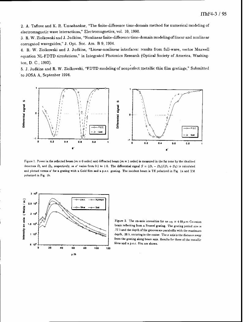
IThF4-3 / 95
2. A. Taflove and K. R. Umashankar, "The finite-difference time-domain method for numerical modeling of
electromagnetic wave interactions," Electromagnetics, vol. 10, 1990.
3. R. W. Ziolkowski and J. Judkins, "Nonlinear finite-difference time-domain modeling of linear and nonlinear
corrugated waveguides," J. Opt. Soc. Am. B 9, 1994.
4. R. W. Ziolkowski and J. Judkins, "Linear-nonlinear interfaces: results from full-wave, vector Maxwell
equation NL-FDTD simulations," in Integrated Photonics Research (Optical Society of America, Washing-
ton, D. C, 1993).
5. J. Judkins and R. W. Ziolkowski, "FDTD modeling of nonperfect metallic thin film gratings," Submitted
to JOSA A, Septenber 1994.
s a
Figure 1. Power in the reflected beam (m = 0 order) and diffracted beam (m = 1 order) is measured in the far zone by the idealized
detectors Di and D2, respectively, as a' varies from 0.1 to 1.0. The differential signal S = (D\ — Di)/(D\ + D?) is calculated
and plotted versus a' for a grating with a Gold film and a p.e.c. grating. The incident beam is TE polarized in Fig. la and TM polarized in Fig. lb.
3 10*n
120
Figure 2. The on-axis intensities for an u0 = 4.68/im Gaussian
beam reflecting from a Fresnel grating. The grating period size is .77 A and the depth of the grooves are parabollic with the maximum depth, .38 A, occuring in the center. The x axis is the distance away
from the grating along beam axis. Results for three of the metallic films and a p.e.c. film are shown.

96 / IThF5-l
Real-time Simulation of the Nonlinear Distortion of Coupled Channel / Interferometric Modulator Designs
Mark L. Farwell and William S. C. Chang Department of Electrical and Computer Engineering
University of California, San Diego La Jolla, California 92093-0407
(619) 534-2737 (tele) (619) 534-2486 (fax)
Introduction
Practical analytic representations of modulator designs are available for only the simplest cases such as the Mach-Zehnder interferometer and the directional coupler. The low frequency dynamic response of the fundamental and nonlinear signals of these modulators are usually described according to their Taylor expansions [1]. However, the frequency response of the fundamental signal for even a simple directional coupler has yet to be expressed in closed form. For modulator designs that are more complex, analytic expressions for the low frequency intensity response are themselves quite complicated, providing little insight into device performance or design optimization. The effect of the RF frequency on the modulator performance (especially the nonlinear distortion) is typically ignored.
Presented here is an algorithm that enables the nonlinear response of a large class of electro- optic modulator designs to be calculated quickly and accurately without requiring an analytic expression for the intensity response of the device. It is a numerical technique based on time- sampling the modulator response to an input one or two-tone test and using a Fourier transform to calculate the various nonlinear signals. This simulation method has many advantages over using a Taylor expansion to model the nonlinearity of a modulator design: (1) Accuracy. This algorithm will be shown to be extremely accurate, due to the optimized choice of parameters in the time sampling / Fourier transform algorithm. Calculating the nonlinear distortion with a Taylor method, on the other hand, can produce erroneous results. This is especially true with linearized modulators where one of the nonlinearities (usually the third order) is compensated (this can be shown to be true even when all significant orders are included in the Taylor expansion). (2) Frequency response. The algorithm allows the electric-optic phase mismatch to be accounted for. This, in turn, allows the fundamental and nonlinear responses at any RF frequency to be calculated. The ability to calculate both the fundamental and nonlinear response of an arbitrary modulator at all frequencies is, to this point, absent from the literature. Since the frequency response of the nonlinear signals is rather non intuitive, this ability is perhaps quite significant. (3) Very dynamic. This method is applicable to any design for which the theoretical intensity can be calculated for any specific input voltage. Since the goal is to evaluate at the design level, a cascade of simple transform matrices is used to represent the entire modulator structure. Using this method, a large class of two channel modulators can be considered. When incorporated with interactive features for adjusting the design parameters and displaying the intensity and phase response as well as the dynamic and frequency response of the nonlinear signals, this method can provide a powerful tool for investigating novel modulator designs.
IThF5-2 / 97
The Optimized Algorithm
The algorithm will be completely developed in this paper. There are three main elements to be presented:
(1) Cascade of matrices model. This allows the intensity versus voltage for any two channel modulator design based on coupling and/or interference effects to be modeled. The component matrices are the standard 2x2 solutions to the coupled mode equations typically used to model simple structures [2]. These matrices are a function of only two parameters: one for the amount of optical coupling across the section and one for the optical phase offset between the two channels. An addition benefit of this method is that the optical phase response is also readily available. From a plot of the phase versus voltage response, the modulator chirp parameter can be determined. Although modulator chirp has become such an important issue, it is typically overlooked.
(2) Time sampling and Fourier transform algorithm. This algorithm is used to calculate the nonlinear distortion for a given modulation depth. A series of such "simulations" results in dynamic response plots for the nonlinear signals desired. One of the major contributions of this paper is in establishing the optimized sampling technique for both a one and two-tone test. Parameters have been determined that limit the calculation error to round-off error (insignificant aliasing and no spectral leakage) while requiring only 32 time samples for the one-tone test and 128 time samples for the two-tone test. The dynamic range for the calculation has been observed to be approximately 260 dB. This algorithm is the heart of the entire simulation program and will be presented in detail.
(3) Accounting for the electric-optic phase mismatch (RF frequency response). The cascade of matrices model lends itself well to incremental subdivision of the actively modulated sections. Following an optical wavefront as it propagates through the active section(s), the phase of the RF signal determining the instantaneous voltage can be appropriately adjusted according to the RF frequency, the active device length, and the difference in electro-optic indices. This process is applicable to both lumped element and traveling-wave electrodes. In this way, the dynamic response of the distortion can be calculated at any arbitrary frequency, or else a frequency response of the distortion (and relative fundamental signal) can be calculated at a fixed modulation depth. In addition, by appropriately attenuating the voltage during the propagation, the effect of microwave loss is also effectively modeled. We have found that only about 20 active section subdivisions are necessary for convergence of this calculation in any case. The real-time nature of the calculation is therefore preserved even for high RF frequency simulation.
Significant Examples
Using a simulation program developed according to this algorithm (on a 486 PC), we have been able to obtain several new results which had not been realized using the conventional Taylor expansion approach. Simulation plots demonstrating a few of these will also be presented:

98 / IThF5-3
Development of the linearized directional coupler modulator [3]
By optimizing the parameters for the bias voltages, we have demonstrated third order compensation and determined the optimal third-order suppression as well as the associated rise in higher order distortion.
Optimized the design layout with respect to the fabrication tolerance and evaluated the tolerance on the bias control.
- Determined the efficiency trade-off and associated chirp parameter.
By evaluating the frequency response of the nonlinear distortion suppression, we have established the linear bandwidth for lumped element electrodes and requirements on traveling- wave electrodes for extending the linear bandwidth.
Investigated distortion suppression by low bias modulator operation [4]
- Established the relationship between the trade-off in increased optical insertion loss and nonlinear distortion suppression for all (odd-order) distortion products.
Improved design for cascaded Mach-Zehnder linearized modulators
Contrary to published results, demonstrated the ability to achieve linearized modulation with equal RF signal on each electrode (no sign reversal required).
Determined the configuration (required coupling values) necessary to achieve third-order distortion that is fifth-order limited for dual cascade, seventh-order for triple cascade, and ninth-order for quadruple cascade (evaluated optimal suppression and tolerance as well).
Determined associated chirp parameter and devised a method for eliminating the chirp.
Improved configuration for high frequency modulators
- Determined that the nonlinear distortion of a reverse AB Mach-Zehnder is significantly reduced with an asymmetric location for the sign reversal.
References
[1] T. R. Halemane, S. K. Korotky, IEEE Trans. Microwave Theory and Tech. 38, 669 (1990). [2] H. Kogelnik and R. V. Schmidt, IEEE J. Quantum Electronics 12, 396 (1976). [3] M. L. Farwell et ai, IEEE Photon. Tech. Lett. 3, 792 (1991). [4] M. L. Farwell, W. S. C. Chang, and D. R. Huber, IEEE Photon. Tech. Lett. 5, 779 (1993).
This work is supported in part by ARPA, Rome Laboratories, Hughes Research Labs, and the California MICRO program.

Thursday, February 23, 1995
Poster Previews
IThG 5:00 pm-5:50 pm Salon 1
100 / IThGl-1
Electrode Design by the Finite Difference Method for Polymer-Based Electro-Optic Modulators
Palle Geltzer Dinesen, Anders Bjarklev, Thomas Rasmussen & Christian Lester Electromagnetics Institute, Technical University of Denmark
DTU, Bldg. 348, DK-2800 Lyngby, Denmark Phone: +45 42 88 14 44, Fax: +45 45 93 16 34
INTRODUCTION: It is well established that electro-optic modulators based on polymers have a strong potential for high-speed applications. Due to the low dispersion over the frequency range from D.C. to optical frequencies, phase matching between a microwave modulation field and an optical field can be obtained, and devices with modulation bandwidths of both 20 GHz [1], and 40 GHz [2] have been demonstrated.
Recently it was shown that even larger modulation bandwidths may be expected by a careful design of the modulator electrode structure in an open microstrip configuration, employing a dielectric buffer layer [3]. In this presentation we investigate the microwave properties of two electrode structures: 1) the open microstrip line with a thick driving electrode and 2) the shielded microstrip line. We calculate the microwave mode index and the characteristic impedance and find that for both structures velocity and impedance matching can be obtained simultaneously.
NUMERICAL METHOD: For a typical electro-optic waveguide structure like in Fig. 1 the dimensions are much smaller (<10 urn) than the wavelength of the microwave modulation field (>3 mm). Thus the field problem is quasi-stationary, and the microwave properties can be solved in the following manner:
We solve the two-dimensional Laplace's equation by a Finite Difference Method (FDM) in a discretized grid where the second order derivatives are replaced by central difference approximations. At the boundaries of the grid we require the potential to be zero, and at the boundary of the driving electrode we specify a voltage V0. In order to simulate an open structure with the implied boundary conditions, a high number of grid points is normally necessary. However, we employ a non-equidistant grid [4] to reduce the number of grid points. The non-equidistant grid is chosen such that the distance between the grid points is large far from the driving electrode and dielectric boundaries, and small in the vicinity of the electrode and dielectric boundaries.
The potential is now determined in two cases: 1) when the structure is air-filled and 2) when the structure is filled with the desired dielectrics. In each of these two cases we calculate the capacitance of the structure as:
C = — (1)
where Q is the charge on the driving electrode, which is calculated by the surface integral:
ID. G = jD-dS (2) s
D is the electric displacement vector. The surface S reduces to a closed curve in the two-dimensional case. With the FDM, (2) reduces to a sum.
When the capacitances for the air-filled structure, C0 and for the structure filled with dielectrics, Cc
are calculated, the microwave mode index (nm) and the characteristic impedance (Z0) can be found as:
n =. — and Z, o :(s/^f 0)
where c is the velocity of light in vacuum.
NUMERICAL CALCULATIONS: We now investigate the structure shown in Fig. 1, [5]. It consists of a three layer waveguide structure between the ground plane and the driving electrode. The thicknesses of the layers are 3.3 urn for the cladding layers and 1,7 pm for the core layer. The static relative
IThGl-2 / 101
dielectric constants are er= 2.9 for the cladding layers and er= 3.5 for the core layer. At 1.32 urn the refractive index of the cladding layers is n=1.551. The core layer is birefringent with a refractive index of rc=1.663 for TM-polarized light. In the transverse direction the optical guidance is introduced by a photo-bleaching process [5]. The electro-optic coefficient for the investigated structure is 15 pm/V.
Employing the Effective Index Method (EIM) we assume a difference in the effective index of 0.005 between the bleached and unbleached parts of the core layer. This leads to a calculated optical mode index of 1.636 for TM-polarized light. In the following we use this figure for comparison with microwave mode index, because when the two mode indices are equal, phase velocity matching occurs.
In [3] we used the Spectral Domain Approach (SDA), [6], to calculate the microwave characteristics of the structure in Fig. 1 with no upper ground plane. We showed that by adjusting the thickness of the microwave buffer layer, velocity matching was possible, and further by adjusting the width of the driving electrode, impedance matching was simultaneously possible. However, the SDA requires that the driving electrode is assumed to be infinitely thin. In order to minimize the conductor loss due to the skin effect, the thickness of the electrode may be around 2-3 urn, and thus the validity of the SDA is questionable. With the FDM described above it is not necessary to assume infinitely thin conductors, and Fig. 2 shows the microwave mode index and the characteristic impedance as functions of the thickness of the driving electrode. The thickness of the buffer layer is adjusted in such a way that it is always 4 urn thicker than the driving electrode, which corresponds to the optimized buffer thickness in the case of an infinitely thin conductor. The width of the electrode is 25 pm.
From Fig. 2 it is clear that the change in the microwave mode index with the electrode thickness is small. However, it can been seen that the change in the characteristic impedance is significant. This means that in designing the modulator it is necessary to take into account the thickness of the driving electrode. In particular, impedance matching which is crucial for the full utilization of the modulator bandwidth is dependent on the thickness of the electrode.
The use of a buffer layer has the draw-back of requiring that part of the microwave field must propagate in air in order to obtain the velocity matching. This means that the structure cannot be pacified by an upper layer (e.g., glass) with a high dielectric constant.
A way of obtaining velocity matching and at the same time pacifying the structure, is to use a shielded microstrip line with a second ground plane on top of the buffer layer (as indicated in Fig. 1). In Fig. 3 we have shown the microwave characteristics for this shielded microstrip configuration with nm and Z0 as functions of the thickness of the buffer layer (equal to the distance between electrode and upper ground plane). The relative dielectric constant of the buffer layer is er=2.5, and the electrode width is 10 urn.
Fig. 3 shows that velocity matching is possible for the shielded microstrip structure. Comparing with the optical mode index of 1.636, Fig. 3 shows that for a shield distance of 5 pm velocity matching occurs. However, the characteristic impedance for this shield distance is as low as 40 Q, which will give a 10 percent reflection if feed from a 50 Q. line.
We can however change the characteristic impedance without changing the velocity matching between the fields. This is demonstrated in Fig. 4. It can be seen, that whereas the microwave mode index is constant on the 4'th digit, the characteristic impedance can be increased from 40 D. to 50 Q. when changing the electrode width from 10 pm to 7 pm.
Thus we have demonstrated that as it was the case for the open microstrip line with a thin buffer layer, the microwave mode index and the characteristic impedance can be matched simultaneously by adjusting the shield distance and the electrode width respectively for the shielded microstrip line.
CONCLUSIONS: We have investigated the microwave properties of an electro-optic modulator by a Finite Difference solution of Laplace's equation in two cases: for a modulator with a thick driving electrode and for a modulator in a shielded microstrip configuration. We have demonstrated that whereas the microwave mode index is only weakly dependent on the thickness of the electrode, the impedance does depend upon the thickness, which consequently must be taken into account in order to obtain impedance matching. Thus we have demonstrated that it is important to use a numerical method which takes the thickness of the electrode into account.

102 / IThGl-3
We have demonstrated that velocity matching is also possible for a shielded microstrip line, which compared to the use of a buffer layer in air has the advantage of giving the possibility of pacifying the structure and at the same time obtain velocity matching. However, the width of the line must be very narrow (7 urn) to obtain impedance matching and this will lead to a higher conductor loss. Also the use of an upper ground plane will introduce additional conductor losses, and thus a trade-off between the bandwidth limitation due to velocity mismatch and conductor losses exists.
REFERENCES [1] Girton, D.G., Kwiatkowski, S.L., Lipscomb, G.F. & Lytel, R.F, Applied Physics Letters, vol. 58,
1991, pp. 1730-1732. [2] Findakly, T. & Teng, C.C., Proc. SPIE, vol. 2025, 1993, pp. 526-534. [3] Dinesen, P.G., Bjarklev, A., Lester, C. & Rasmussen, T., Proc. SPIE, vol. 2212,1994, pp. 657-664. [4] Rasmussen, T. Povlsen, J.H. & Bjarklev, A., IEEE Photon. Technol. Lett., vol. 5, 1993, pp. 339-342. [5] Akzo Electronic Products. Private Communications.
[6] Uwano, T. & Itoh, T.: "Spectral Domain Approach" in Itoh, T. (ed.): "Numerical Techniques for microwave and millimeter waves", Wiley & Sons., 1989.
buffer layer ground plane
- (see text)
driving electrode
ground plane
2 4 Electrode thickness (]jm)
Fig. 1: Cross-section of investigated structure. Upper ground plane is optional (see text).
Fig. 2: Microwave mode index and characteristic impedance as functions of the electrode thickness for unshielded microstrip structure.
Mode index
Char, impedance
10 20 30 Shield distance [\jm)
- 60 Q
3. 50 %
a 40 §
1.634 ■
Mode index
Char, impedance
8 9 Electrode width (]jrn)
O ■48^
44^
Fig 3: Microwave mode index and characteristic impedance for shielded microstrip configuration as function of shield distance.
Fig. 4: Microwave mode index and characteristic impedance for shielded microstrip configuration as function of electrode width.

IThG2-l / 103
Narrow-Band Waveguide Taps Using Photonic Surface Modes Supported by Multilayer Dielectric Stacks
F.D. Lloyd-Lucas, R.D. Pechstedt, T.A. Birks and P.St.J. Russell
Optoelectronics Research Centre, University of Southampton, Southampton S017 1BJ, United Kingdom
Tel +44 703 593172/Fax +44 703 593149 [email protected]
A necessary element, in applications where a widely tunable narrow-band filter is required (e.g., over wavelength at fixed mode index, or over mode index at fixed wavelength), is a structure that supports highly dispersive guided modes whose index may be varied at fixed wavelength. These requirements are satisfied by the photonic surface modes (PSM's) supported on multilayer
silica 1.453
BK7 1.510 oil cladding 1.453
core 1.458
cladding 1.453
■ 5.5 |im b
w
oil cladding 1.453
core 1.458
cladding 1.453
00
D 5
i) ii)
Figure 1. The structures used in the calculations leading to Figures 2 and 3. Evanescent coupling occurs across the low index oil layer. Note that the last layer of the multilayer stack has an index of 3.58 and a thickness of 7.3 nm.
dielectric stacks. PSM's are guided by the interface between a multilayer stack and a low index external medium1,2-3'4. They appear within the photonic band gap or stop-band of the stack, and are confined by total internal reflection and Bragg reflection. A number of special features set them apart from normal waveguide modes. Only one PSM appears per stop-band, and since each stop-band can cover a wide span of effective indices, substantial ranges of quasi-single-mode operation exist. Since it is the Bragg condition that determines the approximate effective index of the PSM's, the average index of the stack can be high, while still permitting phase matching to, for example, a low-index fibre mode. This means that the functionality of the high index III- V system can potentially be married, for example, to low index glass fibre optics. Finally, PSM's are highly dispersive with wavelength and very sensitive to the index of the external

104 / IThG2-2
medium, suggesting applications to narrow-band channel dropping filters and mode-selective couplers - both of which are addressed in this paper. The advantages of using PSM's over less
X (0
1.0
£ 0.5 -
0.0
n 1 1 r
J i i_
825 830
10 -
E E
5 -
0
i i r
835 825 830 835
Figure 2i. The maximum coupling achievable as a function of wavelength for PSM (full line, «j = 1.415) and multimode waveguide (dashed line, «;=1.38) devices (/z = l/mi, t = 2/j.m, w = 2.2^m).
Figure 2ii. Device length at which the maximum coupling of Figure 2i is achieved
dispersive modes (such as those supported by multimode planar waveguides) are also illustrated.The dispersion relation of the PSM's is easily derived using a translation matrix formalism; the details of this derivation are available elsewhere1. PSM's form in the range ß > kne {k is the vacuum wave vector and ne is the index of the external medium), where the propagation constant ß lies within the stop-band of the stack; ß may be tuned over the full stop- band width (and beyond, thus suppressing the PSM) by altering the optical thickness of the final layer of the stack, or by varying the index of the external medium. Both TE and TM polarised PSM's can form, often with widely different values of jS.
In Figure 2, the wavelength sensitivities of coupling from a single-mode planar waveguide to i) a PSM and ii) a higher order mode of a high index planar waveguide are explored. Both structures (see Figure 1) are designed for phase matching at around 830 nm. The maximum coupling, and the coupling length at which this is achieved, are plotted. Note that The PSM device offers more effective narrow-band operation.
In Figure 3, the mode selectivities of coupling from a dual-mode planar waveguide to i) a PSM and ii) the highest order mode of a high index planar waveguide are explored. Tuning is achieved by varying the index n{ of the intervening region. Note that, for a change of 0.006 in «j, the rapid modal dispersion of the PSM allows tuning between the 0th and the 1st order mode, whereas in case ii) only the 0th mode can be phase-matched for the same range of nr The cross-
IThG2-3 / 105
X (0 E
talk, i.e., the coupling from the unwanted mode when tapping out the desired one, is excellent.
Discussion & Conclusions A fibre tap, coupling out a small amount of power in a narrow band around a tunable wavelength, while permitting all the rest to propagate through unchanged, would have important applications as a local receiver in wavelength division multiplexing schemes. The analysis presented in this paper shows that FWHM bandwidths of 0.3 nm should be easily achievable at 830 nm in an AlGaAs stack. Similarly, selective mode coupling at fixed wavelength from multimode fibres would have useful applications in mode- division multiplexing (MDM). Unsuccessful attempts have been
made to achieve MDM using long-range surface plasmon-polaritons supported by a thin metal layer deposited on the side of a side-polished fibre5. This device suffers from poor modal selection as the mode order decreases, leading to significant cross-talk from higher order modes when the device is phase-matched to the fundamental. In addition, high losses are incurred owing to high absorption in the metal, and only TM polarised light can be coupled out. Although (as in the example in Figure 3) planar dielectric waveguides could be used in place of the metal (reducing insertion loss and permitting TE polarised light to couple out), mode selection requires much larger changes in nx than in the PSM device.
n-
Figure 3. coupling versus n{ for PSM (full lines) and ii)
a dual-mode a multi-mode
Maximum waveguide coupled to i) a waveguide (dashed lines). The other parameters are Xvac = 830nm, /z=2/im, r=l/*m, w=5/*m.
In summary, the dependence of PSM effective index on both wavelength and external refractive index is much stronger than for long range surface plasmon-polaritons and conventional planar waveguides. This means that PSM's have great potential in MDM and WDM fibre systems.
References l.
2. 3.
4.
5.
P.St.J. Russell, T.A. Birks and F.D. Lloyd-Lucas, "Photonic Bloch Waves and Photonic Band Gaps," in Confined Electrons and Photons: New Physics and Applications, Eds E. Burstein and C. Weisbuch, Plenum Press, 1994 P. Yeh, "Optical Waves in Layered Media," Wiley, New York (1988). A.A. Bulgakov and V.R. Kovtun, "Study of surface optical oscillations in periodic multi-layer media," Solid State Comm. 56 (781-785) 1985. S.D. Gupta and B. Buti, "Electromagnetic surface waves in periodic layered media," Indian J. Pure & Appl. Phys. 23 (452-457) 1985. S. Barcelos, M.N. Zervas, C. Lavers and P.St.J. Russell, "Mode-selective fibre coupling using long range surface plasmons," presented at LEOS'93, San Jose, California, 1993.
106 / IThG3-l
Form Birefringence of Biconical-Taper Fiber-Optic Couplers under Weakly Fused Condition
Tzong-Lin Wu and Hung-chun Chang
Department of Electrical Engineering and Graduate Institute of
Electro-Optical Engineering, National Taiwan University
Taipei, Taiwan 106-17, Republic of China
Fiber-optic couplers are the key components in many sensor and communication ap-
plications, including wavelength multiplexing and polarization beam splitting. Due to the
deviation of the coupler geometry from circular symmetry, the difference in the coupling
characteristics between x and y polarization states is usually called the form birefringence.
Zheng [1] used the finite-element method to analyze the influence of the coupler's degree of
fusion on the form birefringence. His results showed that weakly fused couplers are non-
birefringent, or isotropic (i.e., the coupling coefficients Cx = Cy) when the degree of fusion
is 1.8 and 2.0 under the assumption that the normalized frequency V = oo. However, for
couplers with longer elongation the V-value in the waist region would not be large. Recently,
Morishita and Takashina [2] have measured the form birefringence for actual fused couplers
and found that the polarization effect is relatively large for weakly fused couplers. To clarify
the discrepancy between the calculated results by Zheng and the experimental results by
Morishita and Takashina, the coupling characteristics at different F-values of the weakly
fused fiber-optic couplers (WFFC), whose degree of fusion falls in the range from 1.8 to 2.0,
is investigated theoretically in this paper using the surface integral equation method [3],
which is based on a vectorial formulation.
Fig. 1 shows the dumbbell-shaped cross-section and the coordinates of the fused coupler,
where 2d is the major width of the coupler, r is the radius of the reduced fiber cladding, and
n\ and n2 are the refractive indices of the coupler and the surrounding medium, respectively.
In the following analysis, rii = 1.45 and n2 = 1 are chosen because in the neck region of
the coupler the light is strongly guided by the boundary between the fiber cladding and the
external medium which is air unless some other potting material is employed. The degree
of fusion of the coupler is defined as d/r. When d/r < 2, the two fibers are fused and the
cross-section is dumbbell-like; when d/r > 2, the two fibers are seperated. The two fibers are
just touching when d/r = 2. The form birefringence is defined by B = (rV2/A3/2)(CX — Cy) ,
where V = (2TT/'\)ryjn\ — n\ is the normalized frequency and A = {n\ — n\)/2n\. The effect
of the degree of fusion on form birefringence of the coupler for different V-values is shown
in Fig. 2, where Zheng's results [1] are also shown by rectangular dots. There is a local
maximum (negative value) of the form birefringence for each V-value. For the WFFC with
large ^-values (V = 30 and 50), this local maximum occurs at the degree of fusion falling
in the region 1.95 < d/r < 2.0. When d/r = 2.0, the polarization effect is still significant
for couplers with large V-values in our analysis. However, the coupler is isotropic at d/r =
IThG3-2 / 107
2.0 in Zheng's results. This discrepancy is due to the fact that under the assumption of V
—► oo, as in Zheng's analysis, the boundary of the fused coupler is like a metal wall and thus
there would be no coupling or no interaction between the two (metal-walled) fibers that are
just touching. Another important feature shown in Fig. 2 is that the isotropic point takes
place at different degree of fusion for different V-value. The dependence of the degree of
fusion at which the coupler is isotropic on the V-value of the coupler is shown in Fig. 3. It
is seen that the degree of fusion at which the coupler is isotropic is asymptotically close to
1.8 as the V-value increases.
In conclusion, the form birefringence of the WFFC at different V-values has been inves-
tigated based on a rigorous vectorial formulation. We have verified that the polarization
effect is still significant as the coupler's degree of fusion approaches 2.0 for large F-values.
The degree of fusion at which the coupler becomes isotropic varies with the F-value and it
is close to 1.8 for large V-values.
REFERENCES
[1] X. H. Zheng, "Finite-element analysis of fused couplers," Electron. Lett., vol. 22, pp.
623-625, 1986. [2] K. Morishita and K. Takashina, "Polarization properties of fused fiber couplers and po-
larizing beamsplitters," J. Lightwave Technoi, vol. 9, pp. 1503-1507, 1991.
[3] C. C. Su, "A surface integral equation method for homogeneous optical fibers and coupled
image lines of arbitrary cross section," IEEE Trans. Microwave Theory Tech., vol. MTT-
33, pp. 1114-1120, 1985.
CM
2d
Fig. 1 The dumbbell-shaped cross-section of the fused coupler.

108 / IThG3-3
1.5
1
V = 5 V = 10
— V = 30 ... v = 50
♦ ♦♦♦ Zheng's results
0.5
-0.5
-1
-1.5
'
•>\ Ft
"1,8 1.85 1.9 1.95 2 2.05 2.1 2.15 2.2
d/r Fig. 2 Form birefringence of the fused couplers as a function of the degree of fusion d/r for V = 5, 10, 30, and 50. Zheng's results in Ref. [1] are also shown.
£.
\ m = 1.45
1.95 \ n2=1.00
\ \ \
d/r 1.9
\ \
\ Isotropie couplers
1.85
"~5 10 15 20 25 30 35 40
V
Fig. 3 Variation of the degree of fusion at which Cx = Cy for the coupler as V increases from 5 to 40.
IThG4-l / 109
Gain-switched Stabilisation of External Cavity Laser Diode Dynamics
L.N.Langley, S.Turovets (+) and K.A.Shore
Bath University School of Electronic and Electrical Engineering
BATH3A2 7AY,UK
Telephone : + 44 225 826272 ; Fax : + 44 225 826305
(+)Permanent address : Institute of Physics, Academy of Sciences, 70 Skarina Ave., Minsk 220072,Republic of Belarus.
Recent advances in the development of techniques for controlling chaos have motivated efforts to implement secure communication systems which exploit the properties of chaotic dynamical systems [1]. An efficient algorithm for improving the locking rate between receiver and transmitter in such systems has been reported recently [2]. An essential ingredient in controlling chaotic dynamics is the procedure for targetting the desired periodic or unstable orbit which will be utilised to carry the desired information.In earlier work [3] it has been shown that periodic orbits can be targeted using loss modulationJn the present work it is demonstrated that gain switching of external cavity laser diodes can be used for targeting periodic orbits.
The theoretical model used here assumes that the laser operates in a single longitudinal mode and is subject to weak optical feedback from an external mirror [4] .When the laser is driven sufficienüy high above its nominal threshold current ,Ljj , the laser dynamics undergoes a period- doubling bifurcation cascade to chaos as the external mirror reflectivity , R , is increased. The application of the targeting procedure when the laser is operated just below the first period- doubling bifurcation point is illustrated in Figure 1 . It is clearly seen from the time dependence of the optical output power given in Fig. la that the targeting to the steady-state occurs using the gain- switching technique. In Fig. lb a carrier-photon density phase-plane representation of the dynamics is given .The initial transient is seen as the phase portrait spirals towards the supposed steady state and then the dynamics evolves along a trajectory leading to the stable limit cycle which represents the final periodic motion.Targeting the laser dynamics in the case of a laser operated just above the first period doubling bifurcation point is illustrated in Figure 2 . The steady-state is clearly visible in thedynamical evolution of the optical output power shown in Fig. 2a as well as in the phase portrait of Figure 2b.
The results obtained here offer a simple practical means for targetting laser diode dynamics. Stabilisation of the laser to the targetted steady state may thence be effected . Attention is now being given to applying control-of-chaos techniques to stabilise unstable orbits of the laser . In turn this may offer the opportunity for ensuring that laser diodes are immune to coherence collapse . Such a technique would appear to be of some practical interest in respect to the hybrid optical integration and packaging of commercial semiconductor lasers.
References
1) S.Hayes ,C.Greboggi, and E.Ott, Phys.Rev.Lett., 70,3031-3034,1993 2) K.A.Shore and D.T.Wright, Electron. Lett ,30,1203-1204,1994 3) V.N.Chizhevsky and S.I. Turovets, Phys. Rev. A , 50,to be published 1994 4) L.N.Langley and K.A.Shore IEEE J. Lightwave Tech.,11,434-441, 1993

110/ IThG4-2
2.0*10
0.0*10°
0 2 3 4 5 6
TIME (ns)
7
7*1020-
9.8*10 9.9*10" 1.0*10" 1.01*1024
CARRIER DENSITY (rrf3)
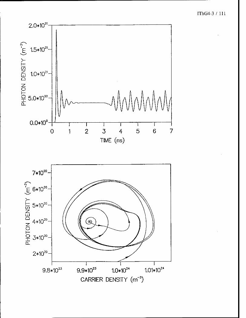
IThG4-3 /111
2.0*10
'E 1.5*1021-
>-
CO
g 1.0*102,~ Q
O
§ 5.0*1020
0.0*10°
12 3 4
TIME (ns)
20 7*10/u-
E 6*10 20
^5*10 20
LÜ Q
O
20 4*10^U-
g 3*1020- Q_
2*10'u-
9.8*10 9.9*10 10*10" 1.01*10"
CARRIER DENSITY (rrf3)
112 / IThG5-l
Self-Consistent Modelling of Diffraction in VCSEL Bragg Stacks
R.R.Burton and M.S.Stern Applied Mathematics Section, School of Mathematics
and Statistics, University of Sheffield, PO Box 597. Sheffield, S10 2 UN, UK
Tel. +44-114-282-4553 Fax +44-114-282-4292
P.C.Kendall and P.N.Robson Department of Electronic and Electrical
Engineering, University of Sheffield, Mappin Street, Sheffield, Si 3JD, UK
Tel. +44-114-282-5131 Fax +44-114-272-6391
Vertical cavity curface emitting lasers (VCSELs) are the subject of much research
at present, given their circular output beam and the ease with which they can be
fabricated into two-dimensional arrays [1]. Very high mirror reflectivities, often as
high as 99.9% [2], are required, due to the short gain region. Since reflectivities
are difficult to measure experimentally, it is necessary to know whether these high
relectivities can be attained in theory. Usually it is assumed that the reflectivity of
a Bragg mirror is given by the plane wave value, ignoring diffraction effects at the
cavity/mirror interface.
We shall consider a substrate-emitting mesa geometry VCSEL shown schematic-
ally in Figs. 1 (a) and 1(b). The cavity region in Fig 1(a) is GaAs, the gain medium
being strained quantum wells (not shown here); attached to this is the Bragg stack,
consisting of alternating quarter-wave layers of AlAs and GaAs. Adjacent to the
VCSEL is air. The VCSEL of Fig 1(b) is identical to that of Fig 1(a) except that
now the cavity region also contains some Bragg layers.
It is well known that radiation into the air at the abrupt refractive index jump
at the GaAs/air interface is small. Ignoring this, we can considerably simplify the
analysis by increasing the dimensions of the cavity to allow for the exponential
penetration of the E-field into the air region [3]. We then set E = 0 along the
new boundaries. To derive an analytical expression for the reflectivity, we take the
Hankel or Fourier transform ip of the held in the cavity (including propagating and
evanescent modes). The transform of the field in the Bragg mirror (d> say) is found
by calculating the transfer function [4]. The TE boundary conditions at the cavity-
mirror interface, in spectral space, are (/», <f, d\\)jdz and df>jdz are continuous at
z = 0, leading us to the exact solution, in the form of a set of linear equations which

IThG5-2 / 113
axe solved iteratively. The first term in the exact solution is seen to be the Fresnel
reflectivity formula [5].
We give below some results for a VCSEL having cylindrical symmetry. The re-
fractive indices riQaAs — 3.5, n^iAs = 3.0, riAir — 1-0 are used, and a free space
wavelength A = l//m is assumed. The incident mode is taken to be the symmet-
ric (no 6 dependence) TE01 mode. Fig. 2 shows reflectivity as a function of cavity
radius, for 20, 25 and 30 Bragg pairs, compared with the plane wave values (dotted),
the configuration of Fig. 1(a) assumed. Thus to obtain 99.9% reflectivity we need 30
pairs when r = 2.8/xm or 25 pairs when r = 3.3/mi. For 20 Bragg pairs external to
the cavity and 5 pairs within it (as in Fig. 1(b)) with r = 2.5/um, the reflectivity is
0.9994, whereas for a 30 pair Bragg stack, as in Fig. 1(a), the reflectivity is 0.9986.
This enhancement is expected: the incident mode, upon meeting the first Bragg layer
embedded in the cavity, suffers negligible diffraction losses. However, such embedded
Bragg layers confine the lateral spread of current and so should be kept to a minimum.
Further results will be presented for the variation of reflectivity with wavelength and
with incident mode number.
References
[1] JEWELL, JACK, HARBISON, J.P., SCHERER, A., LEE, Y.H. and FLOREZ,
L.T.: "Vertical-Cavity Surface-Emitting Lasers: Design, Growth, Fabrication, Char-
acterization" IEEE J. Quantum Electron., 1991, QE-27, 6, pp 1332-1346
[2] SALE, T. E.: Ph.D. thesis, Department of Electronic and Electrical Engineering,
University of Sheffield, 1993, p33
[3] KENDALL, P. C: "Layered theory of the rib waveguide", in ROBSON, P.N.
and KENDALL, P.C. (Eds.): Rib Waveguide Theory by the Spectral Index Method
(Research Studies Press and Wiley, 1990), Optoelectronics Series, Chap. 2, pp9-33
[4] KENDALL, P.C., ROBERTS, D.A., ROBSON, P.N., ADAMS, M.J. and
ROBERTSON, M.J.: "Semiconductor laser facet reflectivities using free-space
radiation modes", IEE Proc. J. 1993, 140, ppl49-55
[5] BABIC, DUBRAVKO I., CHUNG, YOUNGCHUL, DAGLI, NADIR and
BOWERS, JOHN E.: "Modal Reflection of Quarter-Wave Mirrors in Vertical-Cavity
Lasers" IEEE J. Quantum Electron., 1993, QE-29, 6, ppl950-1962

114 / IThG5-3
N BRAGG PAIRS
AIR t AIR
AIR
0
CAVITY
t 2a »
r
AIR
N BRAGG PAIRS
AIR AIR
AIR
o
CAVITY < 2 a •
r
AIR
Fig. 1(a) Fig. 1(b)
2.5 3.0 3.5 4.0
r (m i crons)
Fig. 2
4.5 5.0

IThG6-l / 115
Study of Power Conservation at Waveguide Discontinuities Using the Mode Expansion Method
J. Haes, J. Willems and R. Baets
University of Gent - IMEC, Department of Information Technology Sint-Pietersnieuwstraat 41, B9000 Gent - Belgium
Tel.: +32-9-264 33 16, Fax: +32-9-264 35 93 E-mail: [email protected]
Introduction - It has been shown recently that the mode expansion propagation method [1][2] is an interesting alternative for conventional beam propagation algorithms [3]-[5] to model light propagation in optical waveguides. The method has proved to be fast and accurate for the analysis of periodic waveguides such as codirectional couplers [6] [7]. The most interesting feature of the mode expansion method is that no paraxial approximation is made. The method is therefore able of dealing with large refractive index contrasts and including reflected fields in a natural way. In this paper we take a closer look at the power exchange between modes left and right from a vertical interface (see fig. 1). It will be shown that the neglection of reflections directly impacts on the way the longitudinal power flux needs to be calculated. This is very important when modelling for example tapered waveguides. Here the continuous waveguide profile is stepwise approximated, so that the light propagates through a concatenation of junctions. In the following TE polarised fields in real index slab waveguides will be discussed. The geometry is therefore only two dimensional, one transverse coordinate x and the propagation direction z.
Left
N+1 modes Vk(x-ßk)
Right
N+1 modes Ok(x.Yk)
\
Hv
N>0
ßovo -incident—►
Ztk<t>k i . ,, ZtkYk^k)"transmitted"1
«—reflected—/ v rk^k
\ -Erkßkv|/k
0.4pm
A 1
nC|=3.17
ng=3.3 0.8um )
nC|=3.17 X=1.55pm
Figure I: Field continuity relations at a waveguide junction excited by one mode of the left guide in the TE case.
Figure 2: Junction between a thin and a thick waveguide as in the first example.
Theory - It is well known that Maxwell's equations require continuity of tangential TE field components Ey and Hx at a vertical interface. Assume for simplicity that the incident field consists of only one mode. Hence, with the notations of fig. 1
N N
cont. Ey: V0 + X'W* = X?A (1) k=0 k=0
N N
cont. Hx: ß0i|/0 - 5>*ß*\|/ k=0 k=0
(2)

116 / IThG6-2
2 ßo,er
where ß^ and y^ denote the propagation constants of the respective modes. The summation includes guided modes and a discrete sampling of the continuous spectrum of radiation and evanescent modes. The normalised power flux in the positive z direction Pz+ follows from the definition of the Poynting vector as
N
^Jkh' wim the orthonormality \\\f j\fkdx = \$jtykdx = bik (3) J° *=o s s
where S is the cross section of the calculation window. After projection on the modes <(>£ or \|/^ equations (1) and (2) lead to a linear system of equations that can be solved for reflection r/c and transmission coefficients t^ using standard matrix techniques.
It is common practice to neglect the reflected fields in those situations where one knows that they are weak. Since (1) and (2) cannot be fulfilled at the same time when all r/c = 0, only continuity of one field component can be imposed. If the reflections are negligible most of the incident power will be coupled into the corresponding mode of the right waveguide, having almost the same propagation constant as the incident mode. In this case both equations are almost equivalent. Considering only (1) the transmissions fy equal the overlap integrals
'*=J<MM* (4) s
This value of f& is clearly different from the one obtained from (1) and (2). The normalisation condition in (3) implies directly that, if the set of base functions (modes) <j)£ is complete
N
I'M (5) *=0
and the sum is therefore invariant. When reflections are neglected all incident power is transmitted through the interface and should therefore remain constant while propagating through the structure. Apparently, since (5) defines an invariant, the power flux cannot be given by (3) when reflections are ignored. It is therefore concluded that when reflections at vertical interfaces are neglected the power flux may not be calculated starting from the definition formula of the Poynting vector (resulting in (3)), but is rather given by (5).
Examples - The fact that the longitudinal power flux as defined by (3) produces erroneous results when reflections are ignored can be clearly illustrated by the following example. Consider the waveguide junction of fig. 2. We calculate the power transmission from the left fundamental mode to the right one both using equations (3) and (4), with and without reflections. The incident mode carries unit power. The wavelength is 1.55 |lm and the effective indices of the fundamental modes are 3.213194 (left) and 3.251796 (right). The overlap integral J(f>0\|/0dx = 0.995508 and the transmission coefficient t0= 0.989387 as follows from the solution of (1) and (2). The different power transmissions and the way they are calculated are summarised in the following table.
Pbi = Yo'o / ßo 0.990647 reflections ?0 = solution (1), (2)
Per = YO'O / ßO 1.002942 no reflections t$ = overlap integral
"um ~ h 0.991036 no reflections to = overlap integral
It is obvious that the result Perr > 1 is wrong, while Pfc and Pun[ are almost equal. This proves that the power flux calculation as given by the definition of the Poynting vector produces erroneous results when reflections are neglected. On the other hand the power flux Puni calculated only by means of overlap integrals (when reflections are not considered) seems to be a good approximation of the reality.
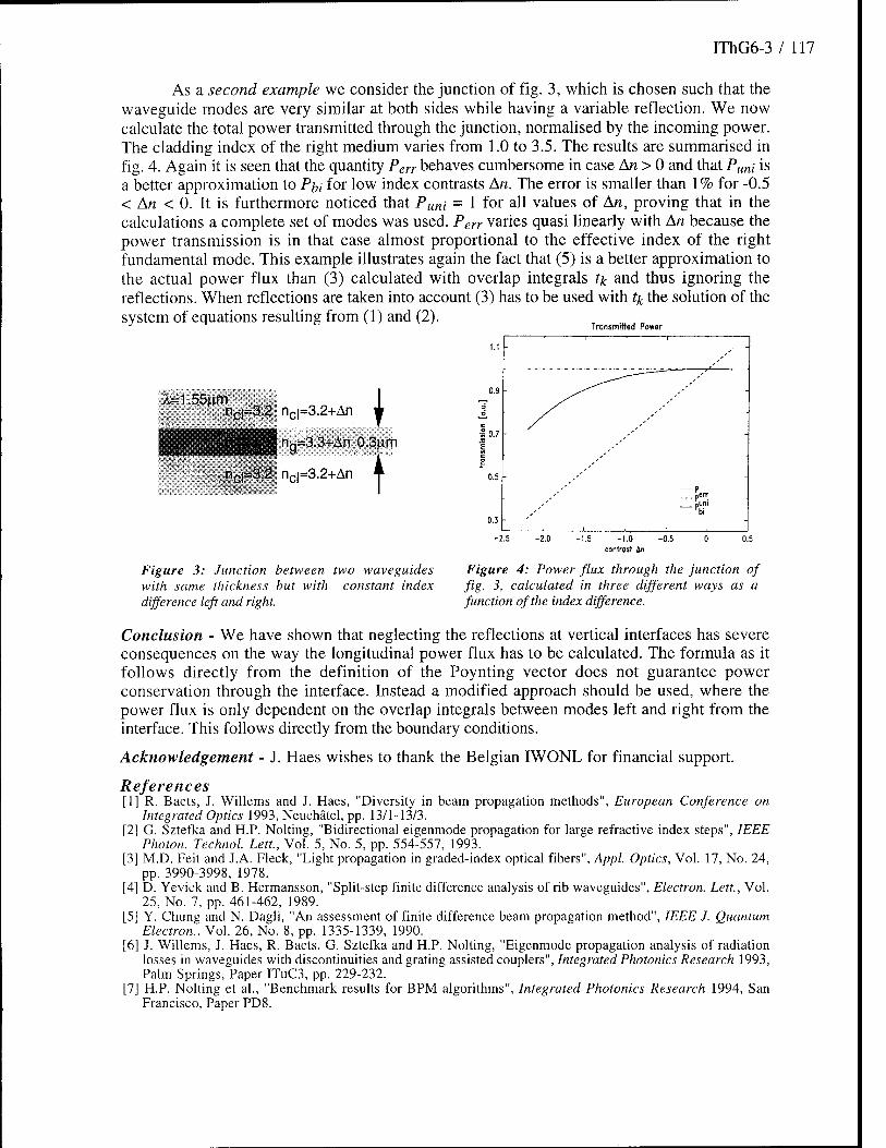
IThG6-3 / 117
As a second example we consider the junction of fig. 3, which is chosen such that the waveguide modes are very similar at both sides while having a variable reflection. We now calculate the total power transmitted through the junction, normalised by the incoming power. The cladding index of the right medium varies from 1.0 to 3.5. The results are summarised in fig. 4. Again it is seen that the quantity Perr behaves cumbersome in case An > 0 and that Puni is a better approximation to P\,i f°r l°w index contrasts An. The error is smaller than 1% for -0.5 < An < 0. It is furthermore noticed that Pun{ = 1 for all values of An, proving that in the calculations a complete set of modes was used. Perr varies quasi linearly with An because the power transmission is in that case almost proportional to the effective index of the right fundamental mode. This example illustrates again the fact that (5) is a better approximation to the actual power flux than (3) calculated with overlap integrals tk and thus ignoring the reflections. When reflections are taken into account (3) has to be used with tk the solution of the system of equations resulting from (1) and (2).
>v=1.55(.im ncp3.2 nc|=3.2+An X
ng=3.3+An 0.3,um
nc|=3.2 nc|=3.2+An J
Figure 3: Junction between two waveguides with same thickness but with constant index difference left and right.
Transmitted Powe r
1.1 - ,-'
,-' 0.9
X '' .-''
0.7 ,' -
S 0.5
,-■'
- P --.perr
Duni
0.3 i ,
-1.0 conlrasi An
-0.5 0.5
Figure 4: Power flux through the junction of fig. 3, calculated in three different ways as a function of the index difference.
Conclusion - We have shown that neglecting the reflections at vertical interfaces has severe consequences on the way the longitudinal power flux has to be calculated. The formula as it follows directly from the definition of the Poynting vector does not guarantee power conservation through the interface. Instead a modified approach should be used, where the power flux is only dependent on the overlap integrals between modes left and right from the interface. This follows directly from the boundary conditions.
Acknowledgement - J. Haes wishes to thank the Belgian IWONL for financial support.
References [1] R. Baets, J. Willems and J. Haes, "Diversity in beam propagation methods", European Conference on
Integrated Optics 1993, Neuchätel, pp. 13/1-13/3. [2] G. Sztefka and H.P. Nolting, "Bidirectional eigenmode propagation for large refractive index steps", IEEE
Photon. Technol. Lett, Vol. 5, No. 5, pp. 554-557, 1993. [3] M.D. Feit and J.A. Fleck, "Light propagation in graded-index optical fibers", Appl. Optics, Vol. 17, No. 24,
pp. 3990-3998, 1978. [4] D. Yevick and B. Hermansson, "Split-step finite difference analysis of rib waveguides", Electron. Lett., Vol.
25, No. 7, pp. 461-462, 1989. [5] Y. Chung and N. Dagli, "An assessment of finite difference beam propagation method", IEEE J. Quantum
Electron., Vol. 26, No. 8, pp. 1335-1339, 1990. [6] J. Willems, J. Haes, R. Baets, G. Sztefka and H.P. Nolting, "Eigenmode propagation analysis of radiation
losses in waveguides with discontinuities and grating assisted couplers", Integrated Photonics Research 1993, Palm Springs, Paper ITuC3, pp. 229-232.
[7] H.P. Nolting et al., "Benchmark results for BPM algorithms", Integrated Photonics Research 1994, San Francisco, Paper PD8.

118 / IThG7-l
Analytical Formulas for Modulation Responses of Complex-Coupled DFB lasers
W. -P. Huang,X. Li and T. Makino1
Department of Electrical and Computer Engineering, University of Waterloo Waterloo, Ontario, Canada N2L 3G1
Telephone: (519)-885-1211, Ext. 5780, Fax: (519)-746-4360
Modulation responses are important for high-speed applications of DFB lasers. Analyti- cal expressions for the small-signal modulation responses are well known and have been used extensively for modeling of dynamic characteristics of seminconductor lasers'1'. These for- mulas are, however, derived from the conventional rate equations. Important effects in DFB lasers such as complex coupling coefficients and spatial-hole burnings are not adaquately considered. To overcome these shortcomings, we have derived approximate formulas for the modulation response of a compelx-coupled DFB laser with arbitrary structures and bias current, based on a rigorous rate equation formulations'2]. It is shown that the AM response can be approximated by
AP(ft) _ % + rR
AP(O) (nR + n - jTR)(nR + n + jTR)
where 0 is the modulation frequency. CtR is the relaxation oscillation frequency expressible by QR = [Q2 — (Ts — FJV)
2/4]2 and TR is the damping rate TR = (Ts + rV)/2. It is noted
that eqs. (1) take idential form to that derived from the conventional rate equations'1], except that the characteristics of the DFB lasers such as the effects of the complex coupling and the longitudinal spatial hole-burning are accounted for rigorously, as reflected by the expressions for 00, TN and T's- When spontaneous emission is neglected, the damping rates for the photons and the carriers may be approximated by
Ts = -S0 — TA / S . —\^^dz 2 ng Jo £ §?dz öS
r,v = "li^fWmW^ (3) Jo
and °2 r [' r™r(a-+^)$2u^i2%
°aAn] AJo l fQ$Hz Jl ' dNym y }
-"■Advanced Technology Labs, BNR, Ottawa, Ontario, Canada K1Y 4H7

IThG7-2 / 119
where S0 is the steady-state photon number, a A the cross sectional area of the active region, r^ the transverse confinement factor, and re the carrier lifetime, c is the light speed in vacuum, ng the group index, and am the material linewidth enhancement factor, $(2) is the normalized longitudinal field distribution and gm is the material gain.
Similarly, the FM response may be given by
A^_^_r r' (am + j)$2 dgm (jft + rs) + D/(jü + T)
Ad" A7rqnglAaeffJo [ ß&dz j dN (ÜR + ft - jTR)(üR + ft + jTR) [)
where ae// is the effective linewidth enhancement factor and D/(jti + T) is caused solely by spatial-hole burning and becomes significant at low frequencies. The expressions for ae//, T and D are a bit lengthy and will not be presented here.
To verify the accuracy of these approximate formulas, we have simulated a complex- coupled DFB lasers. Figures 1 and 2 show the AM and the FM responses at two bias currents for |K/| = 4. It is observed that the approximated formulas are in excellent agreement with the exact solutions.
Reference
[1] G. P. Agrawal and N. K. Dutta, "Semiconductor Lasers," (2nd edition), Van Nostrand Reinhold, New York, 1993.
[2] W. -P. Huang, X. Li, and T. Makino, "A Time-Domain Standing-Wave Approach to Semiconductor Distributed Lasers," IEEE J. Quantum Electron., submitted for publi- cation.

120 / IThG7-3
0.0009
0.0008
0.0007
3 0.0006 CD
Ä 0.0005 CD en c Q- 0.0004 CD
CC
0.0003 -
0.0002
0.0001
0
-
1 I I 1
/ \ltr+40mA
~i 1 1
Solid: exact.
Points: approximate.
> .^**'i*<,%*8a^ltr+80mA - in-phasjp _^&***^ \ ^ K
-
\
\
-
anti-phase %
i i i i i i i
6 8 10 Modulation Frequency (GHz)
Figure 1
12 14 16
70
<:
c o Q. CO CD
CC
anti-phase^tr-niOmA)
Solid: exact. Points: approximate.
6 8 10 Modulation Frequency (GHz)
Figure 2
IThG8-l / 121
Refinement of the Transparent Boundary Condition for Wide Angle Beam Propagation Method
A.M. Sarangan, F. Ma, W.P. Huang
Department of Electrical and Computer Engineering University of Waterloo, Waterloo, Ontario, N2L 3G1, Canada
Tel: (519) 885-1211, Fax: (519) 746-3077
1 Introduction
The transparent boundary condition (TBC) [1] has greatly simplified the use of the Beam Propa- gation Method (BPM). Its primary advantage is that it is problem independent and can be applied with relative ease. Alternative boundary conditions have been studied in the past [2, 3], but they are suitable only for paraxial simulation. The TBC, on the other hand, makes it straightforward to adapt for wide angle BPM e.g. the Pade recursion method [4]. The different TBC methods all assume an outgoing plane wave at the boundaries, and they differ in how this plane wave is modelled. For low order Pade, the angles of incidence at the boundary are shallow and optical energy is typically well confined along the axis. Thus boundary anomalies becomes negligible due to these low fields. Higher Pade orders allow wider propagation angles, so it is more likely for large fields to reach the boundaries at sharper angles of incidence and in a less planar form, e.g. circu- lar wave-fronts. We report a transparent boundary condition suitable for wide angle propagation (WA-TBC), and compare this with the TBC implemented by Hadley [1].
In this poster we systematically study how the outgoing waves appear at the boundaries as the Pade order is increased. The field does not have to be a single plane wave, but can be a superposition of many plane waves, which allows a more accurate representation at the boundary. The method is intuitive and simple to implement for high orders of Pade recursion.
2 Description of the scheme
Consider the left hand side boundary. If the boundary has to allow the waves to pass through, it has to satisfy a relation of the form
where W(k) is a weighting assigned to each plane wave that crosses the boundary. Similarly for the right hand side boundary,
v-iright = £^(*K''4- To ensure that the waves are only out-going, and not entering into the computation window, the values of kx have to be positive and real. Once these values of kx are fully specified to satisfy this condition, the above two equations constitute the two required boundary conditions to completely solve the system.
122 / IThG8-2
The kx values are determined from the z - I step. The weighting function W(k) depends on the angles of the k vectors. It has a maximum contribution when the k vector is directly pointing towards the point where the boundary kx is evaluated, and the contribution decreases as they point away from that point. Figure 3 shows a typical condition for the left boundary. Since the boundary value of kx is evaluated at the midpoint between x = 1 and x = 2, those jfe vectors that point directly at x = 1.5 receive the maximum weighting and the weighting decays towards zero as they point farther away.
3 Simulation Results
As an example we choose the field pattern from a point source at a distance of 0.44/im as the input field. This example was chosen since it includes both extremes of the wide angle and paraxial wave limits. Near the point source the field is highly diverging (at almost 85°) and away from the source it becomes more paraxial. The wavelength is 1.5/zm and the index of the material is uniform at 1.5. Figure 3 shows the resultant field pattern at a distance of 10/im using the paraxial BPM (Pade order 1). The two curves correspond to 1) using Hadley's TBC, and 2) our new WA-TBC scheme. The ideal profile is concave downwards but the simulation result is not. This is attributed to the energy that ideally escapes at wide angles. Figure 3 shows the same field propagated using Pade order 7. The TBC yields spurious reflections whereas the WA-TBC yields a profile that follows the ideal profile.
In our poster we will be showing more details on how this scheme is implemented, and two- dimensional field plots from more test cases.
References
[1] G. Ronald Hadley. Transparent boundary condition for the beam propagation method. IEEE. J. Quantum Elec, 28(l):363-370,1992.
[2] G. Hugh Song. Transparent boundary conditions for beam-propagation analysis from the green's function method. J. Opt. Soc. Am. A, 10(5):896, 1993.
[3] R. Accornero. Finite difference methods for the analysis of integrated optical waveguides. Electronics Letters, 26(23):1959,1990.
[4] G. Ronald Hadley. Wide-angle beam propagation using pade approximant operators. Optics Lett., 17(20):1426-1428, 1992.
IThG8-3 / 123
»3!
ÜD* © iriv-::::©:: © ©
k2 \
© © © ©
Figure 1: A typical left boundary condition showing three plane waves from z = / — 1 contributing towards the boundary value at z = /.
0 50 100 150 200 250 300 350 400 450 500
Figure 2: Field profiles at z = 10/un using Pade order 1.
0.096
0 50 100 150 200 250 300 350 400 450 500
Figure 3: Field profiles at z = 10/xm using Pade order 7.

124 / IThG9-l
Wide-Angle Beam Propagation Modeling of Variable-Angle Photonic Circuits
Igor Ilic, Robert Scarmozzino, Richard M. Osgood, Jr.
Microelectronics Sciences Laboratories 1312 Mudd Building Columbia University New York, NY 10027
Tel. (212) 854-8042 Fax, (212) 932-9421
1. INTRODUCTION The finite-difference beam propagation method using the paraxial approximation1 has been
applied successfully to photonics integrated circuits with shallow angles. Recent extensions to these techniques based on Pade approximants of the square root operator in the one way wave equation2 have made wide-angle propagation possible with a significant improvement in accuracy. However, in order to effectively apply these new techniques to real-world problems, it is necessary to have a thorough understanding of their fundamental limits and how to achieve them. Much of the previous work in this area has focused on implementation and comparison of algorithms using one or two benchmark examples3, rather than considering detailed parametric studies. Here we theoretically examine the Pade-based BPM scheme and derive general expressions for angular and truncation error as a function of various waveguiding and numerical parameters. These results are then validated with numerical experiments. From the general expression for the error, the significance of the choice of reference wavenumber is clearly evident. For waveguiding circuits containing variable angles, the optimal reference wave number, which is normally assumed constant, will change with position , thus we explore the possibility of varying the reference number for efficient solution of variable angle photonic integrated circuits.
2. THEORETICAL STUDY We begin our analytical study by deriving the angular error for propagation in a uniform,
tilted, slab waveguide. This is done by inserting the exact solution to the problem into the wide- angle equations and deriving the error term that results since the exact solution does not satisfy the approximate equation. The one way wave equation is written using Pade approximants:
i!i = ik(jüp--i)U = ikL, , p = JL[Jl + (*=-**)] (i) dz D k* dx2
N(P) and D(P) are defined by the Pade approximation to the square root operator. For simplicity, we evaluate the various derivative that come up in the equation using the exact solution in the area outside the waveguide core, and rewrite the equation (1) as a polynomial expression in terms
IThG9-2 / 125
of a normalizes parameter q, defined as:
[(&-ßcos<))) + j'ysiiKt)] (2)
The equation can than be written as:
N(P) + qD{P) = 0 (3)
By inserting the expression for the Pade approximants, the normalized angular error for Pade(m,n) can be derived as:
t = q(q/2)m+" (4)
3. EXPERIMENTAL STUDY The validity of the above expressions has been tested by numerical experiments which
parametrically study the error dependance on various waveguide and numerical parameters. Our test example for these numerical experiments was a uniform, slab waveguide tilted at an angle from the propagation direction for FD BPM. Since the exact solution is known, it can be compared with numerical results and the error determined by simple measurement of power loss. As an example, this error which is defined as one minus the overlap integral between the exact fundamental mode launched and the output of the tilted waveguide. Figure (1) presents the error as a function of grid-size, with refractive index difference as a parameter. Error approaches a constant error limit, independent of refractive index, a result which can be predicted by expression (4). This limit can then be computed for different angles. The results are shown in Fig. (2) and exhibit the dependance described with sin4 § . Additional parametric studies show similar agreement and will be presented.
Finally, calculation at large angles show that poor choice of reference wave number prohibit accurate results with moderate Pade order. Thus, for smoothly curved bends with large angular spread, error will be significant for some angles independent of the choice of the fixed reference wave number. Therefore we examine a new technique in which the reference wave number is varied along the structure.
4. CONCLUSIONS Expressions for the general angular and truncation error in Pade-based wide-angle schemes
applied to propagation in waveguides have been developed. The theory has been compared with numerical experiments and is in good general agreement. Significant improvement in accuracy for circuits with a number of different angles is achieved with appropriate change of reference wavenumber in the calculation.
REFERENCES [1] R. Scarmozzino and R.M. Osgood, Jr., J.Opt. Soc. Am., vol. A-8, pp. 724-729, 1991. [2] G.R. Hadley, Opt. Lett., vol. 17, pp. 1426-1428, 1992. [3] H.P. Nolting et al, IPR-94 Tech. Dig., San Francisco, 1994.
126 / IThG9-3
in0 i
Fig. 1
At
v . y A /
io-1 -
/ t 1 o IO'2 -
UJ
7 / / / / 7' a
> O 10"3 -
/ A .'/*
/ / 10"4 - Error Limit /
/ /'
\, / A
1CP5 - . . t*n —w KT IO"2
Ax (um)
(Pade (1,0) with k~= ß cos <
TO"1
0.001 G 0.003 B- ■ 0.01
IO"1
UJ 10-3
10-' 10u
Fig. 2
1 f ■■ -"—"T"1"—r,n i i '"1 i" ■" "i y'" 101
Angle (deg)
(Pade (1,0) with k~= ß cos <)>)
Numerical Data o sin4u>
102

IThGlO-1 / 127
STREPE-LOADED MULTIMODE INTERFERENCE COUPLERS
G. M. Berry , S. V. Burke J.M. Heaton Department of Physics and Astronomy Defence Research Agency University of Wales College of Cardiff St Andrews Road
Cardiff CF2 3YB GreatMalvern WR14 3PS United Kingdom United Kingdom
The use of multimode interference (MMT) rib waveguides as couplers/recombiners in passive and active photonic applications has become well established 1>2 and leads to a number of advantages over conventional Y-junction and directional couplers, such as lower losses and shorter propagation lengths. The propagation characteristics of high-wall (deeply etched ribs with strong lateral optical confinement) MMI couplers are well described using the paraxial approximation for the propagation constants of the waveguide, resulting in analytical expressions for the self-imaging length A and power splitting points 3. For many applications stripe- loaded (a shallow etched rib) MMI devices are preferable. For example, Krauss et al 4 suggested, within the context of ring laser integration, a shallow etch would improve overall laser performance as the active layers could remain unexposed and side-wall scattering losses be reduced. However, implications for self-imaging and power splitting performance have not yet been fully investigated. To date modelling of stripe-loaded MMI waveguides has involved either Finite Element5 or Finite Difference6 methods. Unlike analytical methods, these are both time consuming and dependent on the discetization of the mesh, making certain geometric combinations and the modelling of higher-order modes difficult. Here, we present an efficient, semi-analytical approach based on the Spectral Index (SI) method7. The SI method has already been shown to give accurate and fast solutions for single rib waveguides and directional couplers 7.
I. MODEL ,
Figure 1 shows a schematic diagram of a MMI waveguide. Using the SI method we determine the propagation constants and normalised mode profiles of the input, output and multimode sections (let N be the number of guided modes in the multimode section). We then calculate the relative amplitudes of each of these N modes using a two-dimensional field overlap with the input mode profile. The field in the MMI middle section is then represented as a linear combination of the N modes, each propagating with its own phase velocity. To determine the field at the output waveguide interface, and hence the optical throughput, we overlap this field with the normalised mode{s) of the output waveguide.
Light in multimode waveguide
Fig. 1 Schematic diagram of a MW7 recombiner. [The insert shows the waveguide cross-section and all dimensions are in urn.]
The SI method solves the 2-D wave-equation by dividing each of the x-y cross-section into two regions; the rib and slab layers below. The method represents the field in each of these regions using a Fourier series. These field solutions are then matched across the interface using the transfer function method and a variational boundary condition 7.

128 / IThGlO-2
II. APPLICATION
By selecting an appropriate etch depth H, the structure in Figure 1 can represent either a high wall waveguide or a stripe loaded waveguide. We choose 2.4 um wide single-moded input/output waveguides (centrally positioned), a multimode section 9 um wide and a free space wavelength of A.= 1.55 um. (Note: this configuration only excites the symmetric modes of the multimode section.)
Figure 2 shows intensity profiles l(x,z) at the plane of the base of the rib for (a) a high-wall waveguide and (b,c) two stripe-loaded waveguides with etch depths H of 3.01, 1.55 and 1.5 urn respectively. The high-wall waveguide multimode section supports five lateral modes and both stripe-loaded waveguide multimode sections support three lateral modes.
It can be seen from the profiles that as the etch depth is decreased the length at which the 'best' self-image occurs increases. In addition, the reformed image begins to spread and decrease in intensity. This aberration is inevitable in stripe-loaded waveguides as the modal dispersion is non-quadratic resulting in no position along the waveguide at which the phases of all of the modes are identical.
In Figure 3 we assess the quality of the self-imaging process by plotting the throughput (i.e. the ratio of optical power output Iy to optical power input Io) as a function of the multi-mode section length Lz. The plots indicate a number of key points:-
i) The high-wall waveguide plot is symmetric about the 3dB point (Lz=86 urn) and the reformed input image occurs at A=172 um which agrees with the paraxial value A=ngW
2/^=173 urn (where ng is the modal index of the equivalent planar waveguide) for a symmetric input field. Also, the throughput at LZ=A is nearly ideal at 0.995 (indicating only a relatively small amount of de-phasing). ii) For the stripe-loaded waveguides, A=200 and 224 urn for H=T.55 urn and H=1.5 urn respectively, an increase of 16% and 30% over the high-wall waveguide result. In addition, the throughput powers are reduced at only 0.97 and 0.89 respectively.
Figure 4a is a plot of self-imaging length versus etch depth. Figure 4b is a plot of power throughput versus etch depth. We see that an etch depth of at least H=1.52 urn is required to ensure a throughput of at least 0.95.
In summary, we have developed a semi-analytical approach to investigate the propagation characteristics of MMI waveguides. We have presented results showing that the non-quadratic modal dispersion of higher order modes in stripe loaded waveguides impairs the MMI performance.
REFERENCES
Heaton JM, Jenkins RM, Wight DR Parker JT, Birbeck JCH, Hilton KP; Appl. Phys. Lett. 61 1754 (1992) Pcnnings ECM, Den RJ. Schercr A, Bhat R Hayes TR Andreadakis NC, Srrut MK. Soldano LB, Hawkins RJ Appl. Phys. Lett. 59 1926 (1991) Ulrich R Ankele; Appl. Phys. Lett. 27 337 (1995) Krauss T, DeLaRue RM, Gontogol, Layboum PJR; Appl. Phys. Lett. 64 21 (1994) Soldano LB, Bouda M, Smit MK, Verbeck BH; Proceedings of 18th ECOC'92, Berlin (1992)
6 Weinert CM, Agrawal N; IPR94 FH2-2, San Francisco, (1994) 7 Robson PN, Kendall PC (eds.): 'Rib waveguide theory bv the spectral index method' (Research Studies Press and
John Wiley, 1990)

IThGlO-3 / 129
-2.5 0 2.5 -2.5 0 2.5
X (um)
Fig 2. A contour plot of the intensity profile I(x,z) at intervals of 10 percent maximum amplitude. The curves, from left to right, correspond to etch depths ofH=3.01 , H=1.55 and H=1.5 \un.
i\ \
n ii 11
\ A » ' *M A 1 11/ in !\
\ 1 \ I
/ \
\
/\ v i J\ l /N
\ \ V \
A/ !
100 200 300 100 200 300
L (jia)
100 200 300
Fig 3. Throughput L \/lo as a function of middle (Mrvfl) section length LT The curves, from left to right, correspond to etch depths ofH=3.01, H=1.55 and H=L5 \un.
( d )
i \
.5 2.0 2.5 3.0 3.5 .0 1.5 2.0 2.5 3.0 3.5
Fig -I. a). Self-imaging length A as a function of rib height H. b). Throughput I\ i/Io as a function of rib height IT
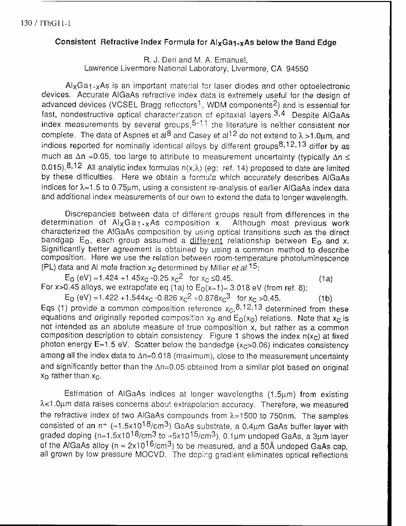
130 / IThGll-1
Consistent Refractive Index Formula for AlxGa-|-xAs below the Band Edge
R. J. Deri and M. A. Emanuel, Lawrence Livermore National Laboratory, Livermore, CA 94550
AlxGai-xAs is an important material for laser diodes and other optoelectronic devices. Accurate AIGaAs refractive index data is extremely useful for the design of advanced devices (VCSEL Bragg reflectors1, WDM components2) and is essential for fast, nondestructive optical characterization of epitaxial layers.3'4 Despite AIGaAs index measurements by several groups,5"11 the literature is neither consistent nor complete. The data of Aspnes et al8 and Casey et al12 do not extend to X >1 .O^im, and indices reported for nominally identical alloys by different groups8-12>13 differ by as much as An =0.05, too large to attribute to measurement uncertainty (typically An < 0.015).8>12 All analytic index formulas n(x,?i) (eg: ref. 14) proposed to date are limited by these difficulties. Here we obtain a formula which accurately describes AIGaAs indices for A,=1.5 to 0.75p.m, using a consistent re-analysis of earlier AIGaAs index data and additional index measurements of our own to extend the data to longer wavelength.
Discrepancies between data of different groups result from differences in the determination of AlxGa-|-xAs composition x. Although most previous work characterized the AIGaAs composition by using optical transitions such as the direct bandgap E0, each group assumed a different relationship between E0 and x. Significantly better agreement is obtained by using a common method to describe composition. Here we use the relation between room-temperature photoluminescence (PL) data and Al mole fraction xc determined by Miller et a/.15:
E0 (eV) =1.424+1.45xc-0.25 xc2 forxc<0.45. (1a)
For x>0.45 alloys, we extrapolate eq (1 a) to E0(x=1 )= 3.018 eV (from ref. 8): Eo(eV)=1.422+1.544xc-0.826xc
2+0.878xc3 forxc>0.45. (1b) Eqs (1) provide a common composition reference xc,8-12'13 determined from these equations and originally reported composition x0 and E0(x0) relations. Note that xc is not intended as an abolute measure of true composition x, but rather as a common composition description to obtain consistency. Figure 1 shows the index n(xc) at fixed photon energy E=1.5 eV. Scatter below the bandedge (xc>0.06) indicates consistency among all the index data to An=0.018 (maximum), close to the measurement uncertainty and significantly better than the An=0.05 obtained from a similar plot based on original xo rather than XQ.
Estimation of AIGaAs indices at longer wavelengths (1.5|im) from existing /U1.0|j.m data raises concerns about extrapolation accuracy. Therefore, we measured the refractive index of two AIGaAs compounds from X,=1500 to 750nm. The samples consisted of an n+ (-1.5x10¹⁸/cm3) GaAs substrate, a 0.4|^m GaAs buffer layer with graded doping (n=1.5x10¹⁸/cm3 to =5x10¹⁵/cm3), 0.1 ^m undoped GaAs, a 3^im layer of the AIGaAs alloy (n - 2x10¹⁶/cm3) to be measured, and a 50Ä undoped GaAs cap, all grown by low pressure MOCVD. The doping gradient eliminates optical reflections

IThGll-2 / 131
from the n+/undoped transition. Alloy compositions were determined to be xc=0.203 based on room temperature PL (eq. 1) and 0.50 based on X-ray diffraction. The index was determined from reflectance spectrum oscillations16 with an accuracy An =±0.015.
To obtain a convenient formula n(A,,x), we fit index data from the literature and our own measurements to a theory derived by Adachi:14
n2(E,x)=80(x) + A(x)*{f(E/Eo)/Eo1 -5 +0.5 f(E/(Es)/Es1 -5} +B(x) g(E/Ei) (2a)
f(y)= [ 2 - (1 +y)0-5 - (1 -y)0-5 ]/y2 (2b) g(E/Ei) = (E/E1 )2 ln[ (1 -E2/Ei 2 ) / (1 -E2/Ei C
2 ) ] (2c) where Eo, Es, and Ei are critical points associated with the alloy band structure, E is the photon energy, E-|C =6.4eV is a cutoff energy, and 8o, A and B are composition- dependent parameters to be determined. E0 is obtained from eqs. (1), and ES=E0+AQ
and Ei are obtained from the literature 8, using our common reference XQ.
A0 (eV) = 0.34 -0.02xc (2d) Ei (eV) = 2.926 +0.6717xc -0.3242xc
2 +0.6172xc3 (2e)
Analytic formulas for Eo(xc), A(xc), and B(xc) in eq. (2a) were determined by iterative least-squares fitting, and will be presented at the conference. Figure 2 compares the fit provided by eqs (2) to experimental data, and Figure 3 shows the maximum and root-mean-square (rms) index deviations |An|max and Anrms for different samples. The maximum fitting error for all samples of Table I is limited to |An|max <0.034 in the range from X= 1.5 to 0.73 |im. This deviation is not representative (Fig. 3), and probably results from imperfect assignment of xc=0.43 to the sample of ref. 13. Ignoring this single sample, the maximum fitting error is |An|max ^0.02 and typical rms deviations are <0.015. These deviations reflect experimental index measurement uncertainties and residual errors in alloy composition XQ.
In conclusion, we have determined an analytical expression for the refractive index n(A,,x) of AlxGai-xAs below the bandgap, which accurately describes experimental data obtained by several different groups to within ±0.02 over the wavelength range from 1.5 to 0.75 |im and the complete range of AIGaAs compositions. Consistency among the data from different groups is achieved by employing a common composition reference. Our results will prove useful for epilayer characterization and the design of advanced optoelectronic components.
We thank Kevin Beernink and Brent Krusor of Xerox PARC for X-ray diffraction analyses and Lan Nguyen for technical assistance. This work was performed under the auspices of the U.S. Department of Energy under contract W-7405-ENG-48.
References 1. J. L Jewell et al., J. Quantum Electron. 27, 1332 (1991). 2. H. Sakata and S. Takeuchi, Photonics Technol. Lett. 3, 899 (1991). 3. L. E. Tarof et al., J. Electron. Materials 18, 361 (1989). 4. E. Kuphal and H. W. Dinges, J. Appl. Phys. 50, 4196 (1979). 5. A. N. Pikhtin and A. D. Yas'kov, Sov. Phys. Semicond. 12, 622 (1978). 6. D. T. F. Marple, J. Appl. Phys. 4, 1241 (1964).

132 / IThGll-3
7. D. D. Sell et al., J. Appl. Phys. 45, 2650 (1974). 8. D. E. Aspnes et al., J. Appl. Phys. 60, 754 (1986). 9. R. E. Fern and A. Onton, J. Appl. Phys. 42, 3499 (1971). 10. M. Garriga et al., Solid State Commun. 61, 157 (1987). 11. K. Hubler et al., Opt. Quantum Electron. 23, S883(1991). 12. H. C. Casey et al., Appl. Phys. Lett. 24, 63 (1974). 13. J. P. Van der Ziel and A. C. Gossard, J. Appl. Phys. 48, 3018 14. S. Adachi, Phys. Rev. B 38, 12345 (1988). 15. N. C. Miller et al., J. Appl. Phys. 57, 512 (1985). 16. M. J. Mondry, et al., Photonics Technol. Lett. 4, 627 (1992).
1977).
3.7
3.5 >
- 3.4 -
2.9 0.8 O 0.2 0.4 0.6
AIGaAs Composition xc
Fig. 1: AIGaAs Index vs. composition xc at 1.5eV photon energy. Data points show experimental results (boxes ref. 8, solid circles this work, open circles ref. 7, triangles refs. 9, 10 and 13). Solid curve shows our formula (eq. 2 in text).
3.8
S 3.4 -
I l l l l
0.5
X?P x-0.207
1.5 2
Photon Energy E (eV)
Fig. 2: Comparison of experimental indices (data points) from this work (diamonds) and the literature (boxes ref. 8, triangles refs. 9, 10, circles refs. 5-7, 12) with our formula (curves). Labels show xc.
Fig. 3: Refractive index deviations between experimental data and the fit obtained using eqs. (2) of the text. Boxes show maximum deviation and circles show rms deviation for Xfrom 750 to 1500 nm.
0 0.2 0.4 0.6 0.8 1
AIGaAs Composition xr
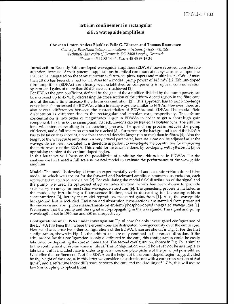
IThG12-l / 133
Erbium confinement in rectangular silica waveguide amplifiers
Christian Lester, Anders Bjarklev, Palle G. Dinesen and Thomas Rasmussen Center for Broadband Telecommunications, Electromagnetics Institute,
Technical University of Denmark, DK-2800 Lyngby, Denmark Phone: + 45 42 88 14 44, Tax: + 45 45 93 16 34
Introduction: Recently Erbium-doped waveguide amplifiers (EDWAs) have received considerable attention, because of their potential applications in optical communication systems as components that can be integrated on the same substrate as filters, couplers, tapers and multiplexers. Gain of more than 10 dB has been obtained for EDWAs for a modest pump power of 145 mW [1]. Erbium-doped fibre amplifiers (EDFAs) are already well established as components in optical communication systems and gains of more than 50 dB have been achieved [2]. For EDFAs the gain coefficient, defined by the gain of the amplifier divided by the pump power, can be increased up to 45 %, by decreasing the cross-section of the erbium-doped region in the fibre core, and at the same time increase the erbium concentration [2]. This approach has to our knowledge never been characterised for EDWAs, which in many ways are similar to EDFAs. However, there are also several differences between the characteristics of EDWAs and EDFAs. The modal field distribution is different due to the rectangular and circular core, respectively. The erbium concentration is two order of magnitudes larger in EDWAs in order to get a short-high gain component; this breaks the assumption, that erbium-ions can be treated as isolated ions. The erbium- ions will interact, resulting in a quenching process. The quenching process reduces the pump efficiency, and a full inversion can not be reached [3]. Furthermore the background loss of the EDWA has to be taken into account, since this is several decades larger (up to five) than in fibres [4]. Also the length of the waveguide amplifier is a very critical parameter, because it can not be adjusted after the waveguide has been fabricated. It is therefore important to investigate the possibilities for improving the performance of the EDWA. This could for instance be done, by co-doping with ytterbium [5] or optimising the size of the erbium-doped region. In this letter we will focus on the possibilities of confining the erbium-ions in EDWAs. For the analysis we have used a full scale numerical model to evaluate the performance of the waveguide amplifier.
Model: The model is developed from an experimentally verified and accurate erbium-doped fibre model, in which we account for the forward and backward amplified spontaneous emission, each represented in 150 frequency slots [2]. For calculating the modal field distribution of the signal and the pump, we used an optimised effective index method, which has been shown to provide satisfactory accuracy for most silica waveguide structures [6]. The quenching process is included in the model, by introducing a fluorescence lifetime, that is decreasing for increasing erbium concentrations [3], hereby the model reproduces measured gains from [1]. Also, the waveguide background loss is included. Emission and absorption cross-sections are sampled from presented fluorescence and absorption measurements on erbium/phosphor-doped integrated waveguides [1]. We assume that the pump and the signal is co-propagating in the waveguide. The signal and pump wavelength is set to 1535 nm and 980 nm, respectively.
Configurations of EDWAs under investigation: Up til now the only investigated configuration of the EDWA has been that, where the erbium-ions are distributed homogeneously over the entire core. Here we characterise two other configurations of the EDWA; these are shown in Fig. 1. For the first configuration, shown in Fig. la, the erbium-ions are only confined in the vertical direction. If the erbium-ions for this configuration is only distributed in the core, this configuration could be easily fabricated by depositing the core in three steps. The second configuration, shown in Fig. lb, is similar to the confinement of erbium-ions in fibres. This configuration would however not be as simple to fabricate, but is included here in order to give a more complete picture of the principal possibilities. We define the confinement, V, of the EDWA, as the height of the erbium-doped region, adot/ divided by the height of the core, a. In this letter we consider a quadratic core with a core cross-section of 6x6 (um)2, and a refractive index difference between the core and the cladding of 1.7 %, this will assure low loss coupling to optical fibres.
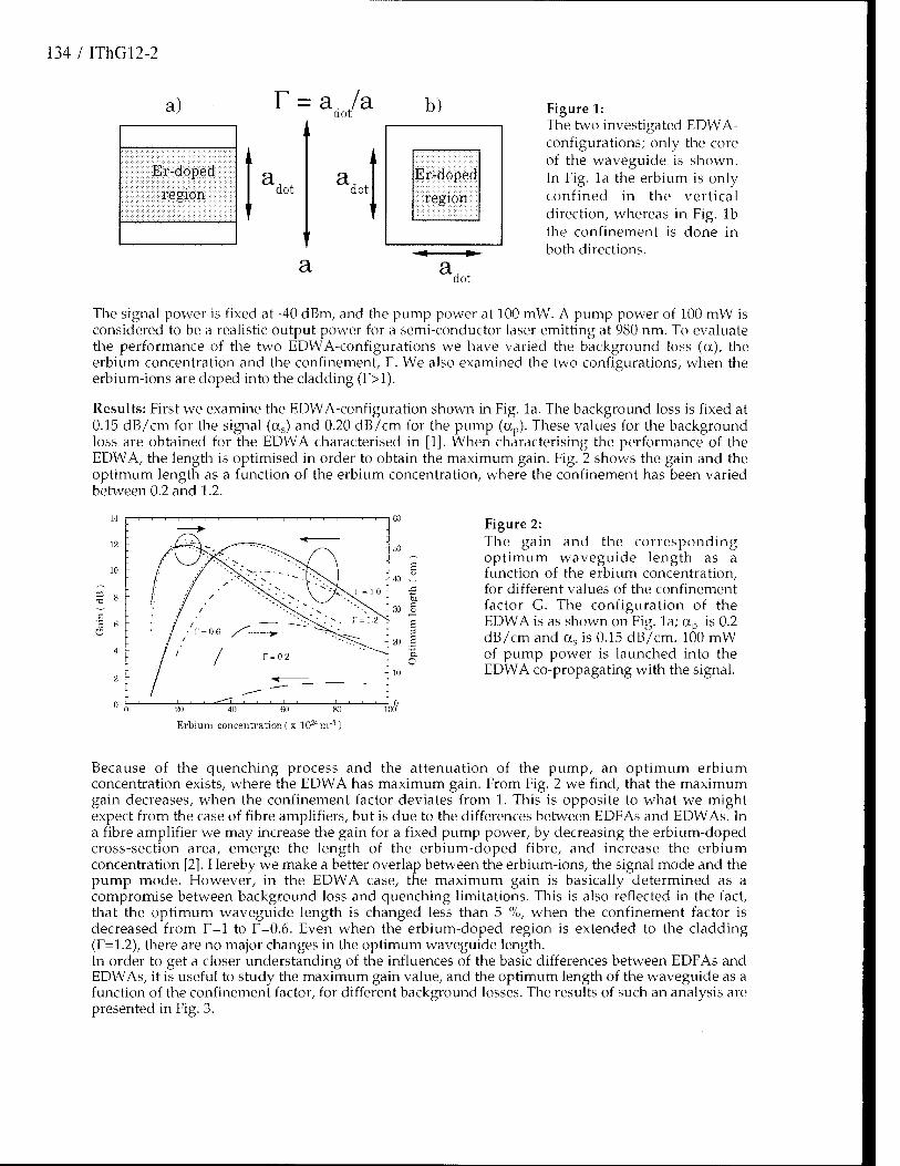
134 / IThG12-2
a) T = a, /a dot b)
Er-doped
region a
dot
a
a dot
1
Er-doped
region
a dot
Figure 1: The two investigated EDWA- configurations; only the core of the waveguide is shown. In Fig. la the erbium is only confined in the vertical direction, whereas in Fig. lb the confinement is done in both directions.
The signal power is fixed at -40 dBm, and the pump power at 100 mW. A pump power of 100 mW is considered to be a realistic output power for a semi-conductor laser emitting at 980 nm. To evaluate the performance of the two EDWA-configurations we have varied the background loss (a), the erbium concentration and the confinement, T. We also examined the two configurations, when the erbium-ions are doped into the cladding (F>1).
Results: First we examine the EDWA-configuration shown in Fig. la. The background loss is fixed at 0.15 dB/cm for the signal (ocs) and 0.20 dB/cm for the pump (ap). These values for the background loss are obtained for the EDWA characterised in [1]. When characterising the performance of the EDWA, the length is optimised in order to obtain the maximum gain. Fig. 2 shows the gain and the optimum length as a function of the erbium concentration, where the confinement has been varied between 0.2 and 1.2.
Figure 2: The gain and the corresponding optimum waveguide length as a function of the erbium concentration, for different values of the confinement factor G. The configuration of the EDWA is as shown on Fig. la; ocp is 0.2 dB/cm and as is 0.15 dB/cm. 100 mW of pump power is launched into the EDWA co-propagating with the signal.
20 40 60 80
Erbium concentration( x lO^m"3)
Because of the quenching process and the attenuation of the pump, an optimum erbium concentration exists, where the EDWA has maximum gain. From Fig. 2 we find, that the maximum gain decreases, when the confinement factor deviates from 1. This is opposite to what we might expect from the case of fibre amplifiers, but is due to the differences between EDFAs and EDWAs. In a fibre amplifier we may increase the gain for a fixed pump power, by decreasing the erbium-doped cross-section area, emerge the length of the erbium-doped fibre, and increase the erbium concentration [2]. Hereby we make a better overlap between the erbium-ions, the signal mode and the pump mode. However, in the EDWA case, the maximum gain is basically determined as a compromise between background loss and quenching limitations. This is also reflected in the fact, that the optimum waveguide length is changed less than 5 %, when the confinement factor is decreased from r=l to r=0.6. Even when the erbium-doped region is extended to the cladding (r=1.2), there are no major changes in the optimum waveguide length. In order to get a closer understanding of the influences of the basic differences between EDFAs and EDWAs, it is useful to study the maximum gain value, and the optimum length of the waveguide as a function of the confinement factor, for different background losses. The results of such an analysis are presented in Fig. 3.
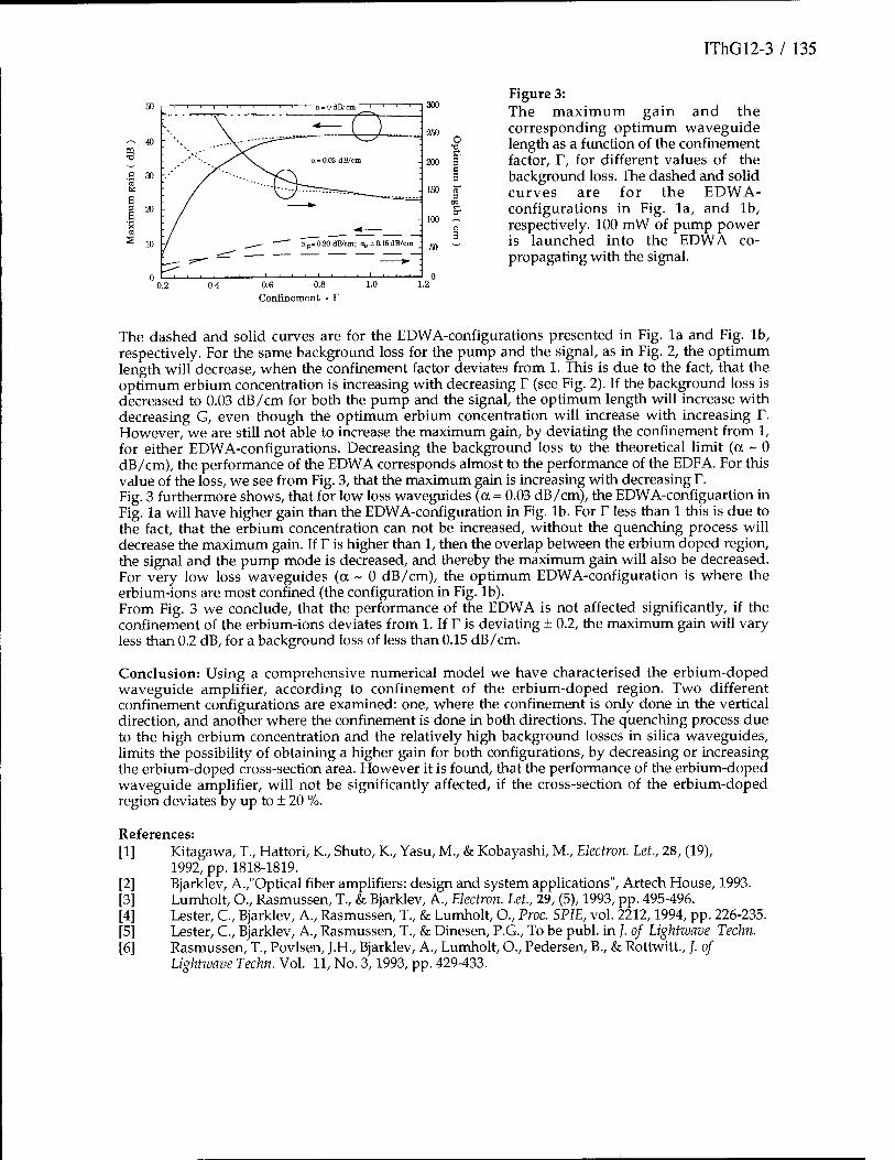
IThG12-3 / 135
Figure 3: The maximum gain and the corresponding optimum waveguide length as a function of the confinement factor, r, for different values of the background loss. The dashed and solid curves are for the EDWA- configurations in Fig. la, and lb, respectively. 100 mW of pump power is launched into the EDWA co- propagating with the signal.
0.6 0.8 Confinement - r
The dashed and solid curves are for the EDWA-configurations presented in Fig. la and Fig. lb, respectively. For the same background loss for the pump and the signal, as in Fig. 2, the optimum length will decrease, when the confinement factor deviates from 1. This is due to the fact, that the optimum erbium concentration is increasing with decreasing r (see Fig. 2). If the background loss is decreased to 0.03 dB/cm for both the pump and the signal, the optimum length will increase with decreasing G, even though the optimum erbium concentration will increase with increasing T. However, we are still not able to increase the maximum gain, by deviating the confinement from 1, for either EDWA-configurations. Decreasing the background loss to the theoretical limit (a ~ 0 dB/cm), the performance of the EDWA corresponds almost to the performance of the EDFA. For this value of the loss, we see from Fig. 3, that the maximum gain is increasing with decreasing r. Fig. 3 furthermore shows, that for low loss waveguides (a = 0.03 dB/cm), the EDWA-configuartion in Fig. la will have higher gain than the EDWA-configuration in Fig. lb. For F less than 1 this is due to the fact, that the erbium concentration can not be increased, without the quenching process will decrease the maximum gain. If T is higher than 1, then the overlap between the erbium doped region, the signal and the pump mode is decreased, and thereby the maximum gain will also be decreased. For very low loss waveguides (a ~ 0 dB/cm), the optimum EDWA-configuration is where the erbium-ions are most confined (the configuration in Fig. lb). From Fig. 3 we conclude, that the performance of the EDWA is not affected significantly, if the confinement of the erbium-ions deviates from 1. If T is deviating ± 0.2, the maximum gain will vary less than 0.2 dB, for a background loss of less than 0.15 dB/cm.
Conclusion: Using a comprehensive numerical model we have characterised the erbium-doped waveguide amplifier, according to confinement of the erbium-doped region. Two different confinement configurations are examined: one, where the confinement is only done in the vertical direction, and another where the confinement is done in both directions. The quenching process due to the high erbium concentration and the relatively high background losses in silica waveguides, limits the possibility of obtaining a higher gain for both configurations, by decreasing or increasing the erbium-doped cross-section area. However it is found, that the performance of the erbium-doped waveguide amplifier, will not be significantly affected, if the cross-section of the erbium-doped region deviates by up to ± 20 %.
References: [1] Kitagawa, T., Hattori, K., Shuto, K., Yasu, M., & Kobayashi, M., Electron. Let, 28, (19),
1992, pp. 1818-1819. [2] Bjarklev, A.,"Optical fiber amplifiers: design and system applications", Artech House, 1993. [3] Lumholt, O., Rasmussen, T., & Bjarklev, A., Electron. Let, 29, (5), 1993, pp. 495-496. [4] Lester, C, Bjarklev, A., Rasmussen, T., & Lumholt, O., Proc. SPIE, vol. 2212,1994, pp. 226-235. [5] Lester, C, Bjarklev, A., Rasmussen, T., & Dinesen, P.G., To be publ. in /. of Lightwave Techn. [6] Rasmussen, T., Povlsen, J.H., Bjarklev, A., Lumholt, O., Pedersen, B., & Rottwitt., /. of
Lightwave Techn. Vol. 11, No. 3,1993, pp. 429-433.
136 / IThG13-l
Analysis of Dispersion Penalty with Chirp Gratings
in 10 Gb/s Systems.
K. K. Goel, 1,F. Ouellette,2
department of Electrical Engineering/OFTC,
University of Sydney, NSW 2006, Australia
Tel. 61-2-692-4866, Fax 61-2-692-3847
2OFTC, University of Sydney
IThG13-2 / 137
Dispersion is a significant factor limiting the maximum bit rate-distance in future
high speed, long distance optical fiber systems. It causes significant signal degradation when com-
bined with chirping introduced by the semiconductor laser. The signal degradation is caused in
terms spreading of the optical pulses. The resulting intersymbol interference can cause a signifi-
cant performance degradation and since degradation increases with bit rate and length of optical
fiber, it results in lower repeater spacings. With the increased use of doped optical amplifiers to
compensate for the loss, a device which can combat the spreading of the optical pulses will result
in a higher bit rate and hence longer repeater spacing. A structure which is capable of providing
dispersion characteristics opposite to that of the fiber could serve as an useful optical pulse equal-
izer. For example, a single mode fiber with strong chromatic dispersion characteristics at the oper-
ating wavelength but opposite in sign to that of the transmitting fiber can be used. A number of
optical domain techniques have been used to compensate the dispersion. These include reflective
Fabry-Perot, cascaded mac Zehnder interferometers, mid-system phase conjugation, waveguide
grating filters, chirped gratings in the fiber. There are recent experimental system demonstrations
of dispersion compensation with bragg In-fiber gratings using external modulation with fixed
chirp[l,2]. Recently [3] a 2 cm long grating dispersion compensation has been simulated for elec-
troabsorption modulator system at 10 Gb/s.
In this paper, we present a systematic study of dispersion penalty introduced by the in-
fiber chirp gratings for external modulated and direct modulated systems at 10 Gb/s. We have
studied the grating chirp variation and its effect on the useful fiber length. It is shown that an opti-
mum length of fiber exists for a given grating structure. This study is aimed at determining the
optimum grating structure and maximum repeater spacing possible with grating compensator at
10 Gb/s. Here we show an example of a design in which a 4cm long grating is used to compen-
sate the dispersion of standard optical fiber with less than 1 dB penalty. In our calculations we
assume a standard fiber with dispersion of 17 ps/nm/km. In the simulation, NRZ data signal is
generated and passed through optical fiber which introduces linear group delay. The fiber output is
passed through the chirp grating structure and delected by photo diode and 8 Ghz third order but-
138 / IThG13-3
terworth low pass filter. Figure 1 shows the calculated results for 4 cm (0.10 nm/cm chirp) & 5 cm
(0.075 nm/cm chirp) long in-fiber chirped bragg gratings with coupling strength of 3.0 cm-1 and
have gaussian amplitude envelope. The simulated result shows that dispersion penalty changes
with length of the fiber link and there exists a range of useful fiber length for 1 dB. penalty. Figure
2 shows the calculated results of dispersion penalty for direct laser modulated system with uni-
form chirp. These results are calculated for a 4cm long in-fiber grating with 0.1 nm/cm chirp. A
peaked behavior suggests the useful optimum length of dispersion compensation. However, dis-
persion penalty occurs if fiber length other than optimum is chosen. Figure 3 shows the calculated
eye pattern for a 75 Km long optical fiber system with chirp grating compensator. It has been
shown in experimental system demonstrations [1,2, 4] that dispersion penalty in optical fiber sys-
tems can be reduced in external modulated systems by adjusting the chirp. We have also calcu-
lated the dispersion penalty of the in-fiber bragg gratings for external modulated systems with
positive and negative chirp. Figure 4 show the results of dispersion penalty as a function of fiber
length for chirp-less and chirped external modulation. Fixed chirp in external modulation system
improves the performance by 0.2 dB. over the chirp-less external modulation.
References
[1] B. Malo, et.al,"Dispersion compensation of a 100 km, 10 Gb/s Optical fiber link
using a chirped In-fiber bragg grating with a linear dispersion characteristics,"
Post-deadline paper, pp. 23-26, Vol. 4, ECOC'94.
[2] D. Garthe, et.al," Practical dispersion equalizer based on fiber gratings with bitrate
length product of 1.6 Tb/S.Km," Post-deadline paper, pp. 11-14, Vol. 4, ECOC'94
■ [3] P. L. Mason, R. V Pentry and I. H. White, "Multiple Stage Dispersion Compensa
tion in Long Haul Optical Fiber Systems Using Chirped Fiber Bragg Gratings,"
IEE Electronics Letters, Vol. 30, No. 15, pp 1244-1245, July 1994.
[4] A. H. Gnauck, et.al "Dispersion Penalty Reduction Using an Optical Modulator
with Adjustable Chirp,"IEEE Photonics Technology Letters, vol. 3, No. 10, pp.
916-918, August 1990.
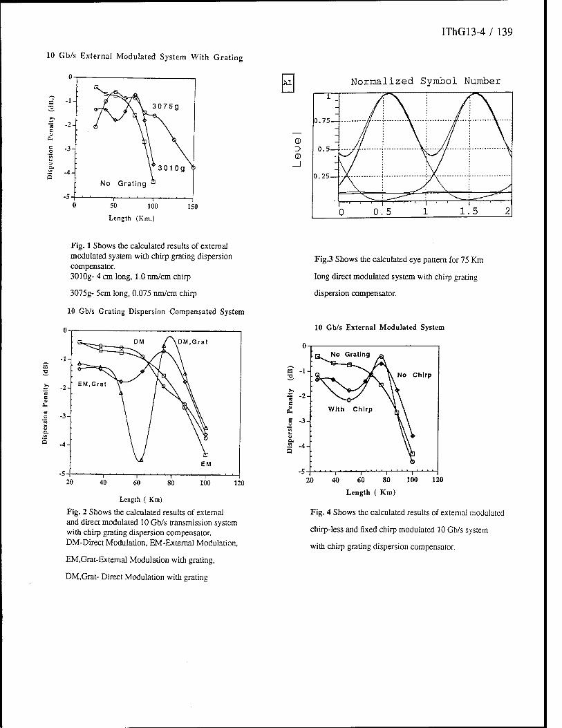
IThG13-4 / 139
10 Gb/s External Modulated System With Grating
0-
100
Length (Km.)
150
Al
(D I> CD
Normalized Symbol Number
Fig. 1 Shows the calculated results of external modulated system with chirp grating dispersion compensator. 3010g- 4 cm long, 1.0 nm/cm chirp
3075g- 5cm long, 0.075 nm/cm chirp
10 Gb/s Grating Dispersion Compensated System
DM,Grat
120
Length ( Km)
Fig. 2 Shows the calculated results of external and direct modulated 10 Gb/s transmission system with chirp grating dispersion compensator. DM-Direct Modulation, EM-External Modulation,
EM.Grat-Extemal Modulation with grating,
DM,Grat- Direct Modulation with grating
Fig3 Shows the calculated eye pattern for 75 Km
long direct modulated system with chirp grating
dispersion compensator.
10 Gb/s External Modulated System
a ■a
No Grating
No Chirp
Length ( Km)
Fig. 4 Shows the calculated results of external modulated
chirp-less and fixed chirp modulated 10 Gb/s system
with chirp grating dispersion compensator.
140 / IThG14-l
The Use of a Sparse Matrix Eigenmode Solver in Semivectorial Finite Difference Modelling of Optical
Waveguides
M.S. Stern*, C.L. Xu, F. Ma, W.P. Huang
Department of Electrical and Computer Engineering University of Waterloo, Waterloo, Ontario, N2L 3G1, Canada
Tel: 519-885-1211 (Ext. 5819) Fax: 519-746-3077
* On leave from: Applied Mathematics Section, School of Mathematics & Statistics, University of Sheffield, PO Box 597, Sheffield, S10 2UN, UK
Tel: +44-114-282-4553 Fax: +44-114-282-4292
Semivectorial finite difference (SVFD) schemes have been successfully employed for the direct determination of eigenmodes of optical waveguides with arbitrary transverse refractive index profiles n(x,y) [1, 2]. Two ways of solving the resulting eigenvalue problem have been
(i) the inverse power iteration methodfl], which involves the solution of a nonsymmetric or nonHermitian matrix, and
(ii) the Rayleigh quotient method[2], which is limited in the modes that it can find by symmetry requirements and by accuracy of the initial guess.
We have significantly reduced the memory and computing time required by the inverse power iteration method by using the iterative matrix solver BICGSTAB[3] with incomplete LU (ILU) factorizaton[4].
The principal advantage of (i) is that it can determine any desired eigenmode (propagation constant plus field profile) of a waveguide structure. Its main disadvantage has been the computer memory required to solve the matrix directly with complete LU factorization (CLU). Although CLU preserves the bandwidth of SVFD matrices, it does not preserve their sparse diagonal structure due to considerable non-zero fill-in of the band. Thus storage has to be allocated for the whole band (but not for the regions situated above and below the band). For a uniform or graded finite difference mesh containing Nx and Ny grid points in the x and y directions, respectively, the number of array elements that have to be stored for CLU is
S(CLU) = (2M + l)NxNy (1)
where M = min(Nx,Ny). The main advantage of (ii) is that no matrix storage is required. Computer memory is allocated only for the values of n(x,y) and the field profile at the NxNy
mesh points. Thus the number of array elements that have to be stored is only
S(RQ) = 2NxNy (2)
However, RQ can only find the fundamental symmetric and leading antisymmetric polarised modes of waveguide structures which possess left-right symmetry (or just the lowest order
IThG14-2 / 141
mode of structures not possessing such symmetry). Higher order modes can be found only if an accurate initial approximation to that mode's field profile is available.
Applying BICGSTAB with ILU to the inverse power iteration method overcomes the limita- tions of both (i) and (ii), since the bandwidth and the sparsity pattern of the matrices can be preserved. The number of array elements requiring storage is
S(ILU) = 20NxNy (3)
By comparing equations (1),(2),(3), we see that
S(CLU)/S(RQ) = (2M + l)/2 S{CLU)/S(ILU) = (2M + l)/20 { }
Further, our new sparse matrix eigenmode solver has all the advantages of (i) and (ii), but none of their disadvantages. We observe from the second ratio in (4) that relative memory reduction begins with M > 9, which is always the case in practical simulations. Figure 1 shows data to support this. The memory savings of the iterative solver starts to diminish for very small mesh sizes due to fixed overhead e.g. storage for refractive index profile and the field.
Finally, a comparison of execution time shows that, for comparable accuracy, the iterative solver is faster when execution times are large. Figure 2 shows an approximately linear dependence with mesh size for the iterative solver, while the the direct solver time increases superlinearly (theoretically, a quadratic relationship).
In conclusion, we have combined a semivectorial finite difference mode solver with the BICGSTAB iterative sparse matrix solver using ILU factorization. The memory and com- putation time required have a linear rather than quadratic dependence on mesh size, and the full functionality of the inverse power iteration method is retained.
References
[1] M.S. Stern: "Semivectorial Polarised Finite Difference Method For Optical Waveguides With Arbitrary Index Profiles", IEE Proc J 135 (1988) 56-63.
[2] M.S. Stern: "Rayleigh Quotient Solution of Semivectorial Field Problems for Optical Waveguides with Arbitrary Index Profiles", IEE Proc. J 138 (1991) 185-190.
[3] H.A. Van der Vorst: "BI-CGSTAB: A Fast and Smoothly Converging Variant of BI-CG for the Solution of Non-Symmetric Linear Systems", SIAM J. Sei. Stat. Comput. 13 (1992) 631-644.
[4] I. Gustafsson: "On Modified Incomplete Factorization Methods" in J. Hinze, editor, Numerical Integration of Differential Equations and large Linear Systems, number 968 in Lecture Notes in Mathematics. Springer-Verlag, 1982

142 / IThG14-3
4-1
o S
O H
50
20
10
5
0.5
Figure 1:
Memory Requirement, Direct-Solve vs. ILU/BICGSTAB
10
1 1 1 ..-;-' ITERATIVE Ny=200
DIRECT i /J i .----"" !•-' '" _.-'
! J\-f'''~~"P L.---"" \.--r /Ny=Njc ~L^^
i
i
Ny=100
20 50 Nx [Mesh Points]
100
700 , , T3 600 C O
500 l__J
o E 400 H e o 300 3 O
X 200 m <—H rt 100 O H
Figure 2:
Execution Time, Direct-Solve vs. ILU/BICGSTAB 1 1 1
IL|J/BIC<}STAB; 1 1 1 1 1 1 1 1 1 1 I 1 1 1 1
LU ̂ direct
I 1 1 1 1 1 1 1 1 1 ,•'.'
1 1 1 1 1 .* •' i i , Ny^Nx y ,r
1 1 1 1 K .' 1,'
l}fy=20Ö !\ \A/ ! i JK i \\ .'i A i
1 '1 \\ '-' \ \' \ '
. ■ » i i i b
i ' 1. -'' ' -'' \ Jhsr^^fJ^-^^
_____^^—T .. i - '.^^^^ ^ i j -
—Lü: [— f , , ,
0 20 40 60 80 100 120 Nx [Mesh Points]
140 160 180 200
IThG15-l / 143
Guided-Wave Acousto-Optic Bragg Diffractions in InP/InGaAsP/InP Waveguide B. Sun, A. Kar-Roy, and C. S. Tsai
Department of Electrical and Computer Engineering and Institute for Surface and Interface Science
University of California, Irvine Irvine, CA 92717, U.S.A.
Tel# (714)856-5144; Fax# (714)725-3732
The integrated acoustooptic (AO) device Modules that utilize Bragg diffraction of guided-optical waves from surface acoustic waves (SAW) in LiNb03 planar optical waveguides have been shown to be capable of performing a variety of useful functions in RF signal processing, optical communications, and analog electrooptic computing[l]. However, only a partial or hybrid integration of such AO device modules can be realized at present due to the inability of monolithically integrating lasers and photodetectors on a common LiNb03 substrate. InP substrate can potentially provide the capability for total or monolithic integration because both the laser sources and the photodetectors as well as the associated electronic devices have been successfully integrated in the same substrate [2]. More importantly, InGaAsP/InP lattice-matched heterostructures, QW lasers and other photonic devices operating at the desirable optical wavelengths of 1300 and 1500nm are being realized for applications in fiber optic communication systems[3]. In this paper, we report the first theoretical and experimental studies of guided-wave AO Bragg diffraction in a composite InP/InGaAsP/InP planar waveguide structure. Relatively good diffraction efficiency has been accomplished at 1310nm optical wavelength using the SAW at the center frequency of 167 MHz and an acoustic interaction length as small as 1.0mm.
A pure Rayleigh SAW wave can be excited and propagated along the <110> direction of Z-cut InP substrate. The calculated and measured propagation losses associated with such SAWs are also desirably low[4]. Also, the measured elastooptic properties of bulk InP crystals have suggested a large AO figure of merit comparable to that of GaAs[5]. Finally, the cleavage planes for the Z-cut InP substrate are known to be along the <110> and <1 1 0> directions. Based on the desirable technical factors just mentioned, the <110>- propagating SAW on the Z-cut InP substrate was chosen for the experimental study of guided-wave AO Bragg diffraction. Note that the relevant guided- optical waves propagating in directions nearly orthogonal to that of the SAW could be conveniently coupled through the cleaved facets along the <110> direction to facilitate experimental studies.
Fig. 1 shows the configuration of the guided-wave AO Bragg diffraction on the Z- cut {001} semi-insulating InP waveguide substrate used. The waveguide sample is composed of three layers: 0.017 urn InP buffer layer, 0.35 um InGaAsP guiding layer, and 0.5 urn InP cap layer. A 0.25 um piezoelectric film of ZnO was deposited on the top of the InP/InGaAsP/InP composite waveguide to enhance the transduction efficiency for
144 / IThG15-2
the SAW. Numerical calculations have shown that addition of the ZnO over layer does not significantly alter the optical field distributions as the light beam is well confined within the InP/InGaAsP/InP waveguide. The InP/InGaAsP/InP waveguide sample was first cleaved to the size of 4x6mm2. A 0.25 um ZnO film overlayer was subsequently deposited by RF sputtering. The pairs of the interdigital transducers(IDTs) each had an aperture of 1.0 mm and 25.5 electrode finger pairs with a finger periodicity of 16 pm, and separated by 2.5 mm, were fabricated upon the ZnO film.
Pulsed RF driving signals at the center frequency of 167 MHz were utilized for measurement of the transduction loss of the IDTs, the propagation characteristics of the SAW, and the characteristics of the resulting guided-wave AO Bragg diffractions. The two-way conversion loss for the transducer at the absence of any impedance matching was measured to be 51 dB at the acoustic frequency of 167 MHz.
For the AO Bragg diffraction efficiency measurement, a 1.0 us pulsed RF signal, having a pulse width significantly greater than the acoustic transit time for the aperture(~lmm) of the incident guided-optical wave, was first applied to the transmitting IDT. The depletion in the undiffracted light power and the corresponding increase in the diffracted light power were then measured. Fig. 2 shows the photograph of the Bragg- diffracted and undiffracted light beams. The measured diffraction efficiencies for the TE0- and TM0- modes light at the acoustic center frequency of 167 MHz are 1.41 and 0.95%, respectively, at the acoustic drive power of 0.85 milliwatt. We note that when the incident light was propagated in the TE0-mode a diffraction efficiency of 14% was measured at an acoustic drive power of only 8.5 milliwatts.
In conclusion, guided-wave AO Bragg diffractions in the InP/InGaAsP/InP waveguide structure has been analyzed using coupled-mode technique and measured for the first time. Diffraction efficiency as high as 14% has been accomplished at an acoustic drive power of 8.5 milliwatts using an acoustic interaction length of only 1.00mm. The relatively high RF drive power measured (5 watts )was mainly due to the high conversion loss of the IDT transducer, namely, 25.5dB. Based on our theoretical predictions improvement in diffraction efficiency in terms of per mm acoustic interaction length per watt RF drive power by as much as three orders of magnitude can be achieved by incorporating the following changes in a new design: (a) optimizing the thickness of ZnO film to utilize enhanced electromechanical coupling coefficient, (b) optimizing the layer thicknesses of the composite waveguide to achieve increased overlap integral between the optical and acoustic fields, (c) inserting an impedance matching circuit to minimize the transducer conversion loss, and (d) enlarging the transducer aperture and thus the interaction length by five -to ten- fold.
The authors wish to express sincere thanks to Drs. R. Bhat and H. P. Lee of Bellcore for supplying the samples used in this work.
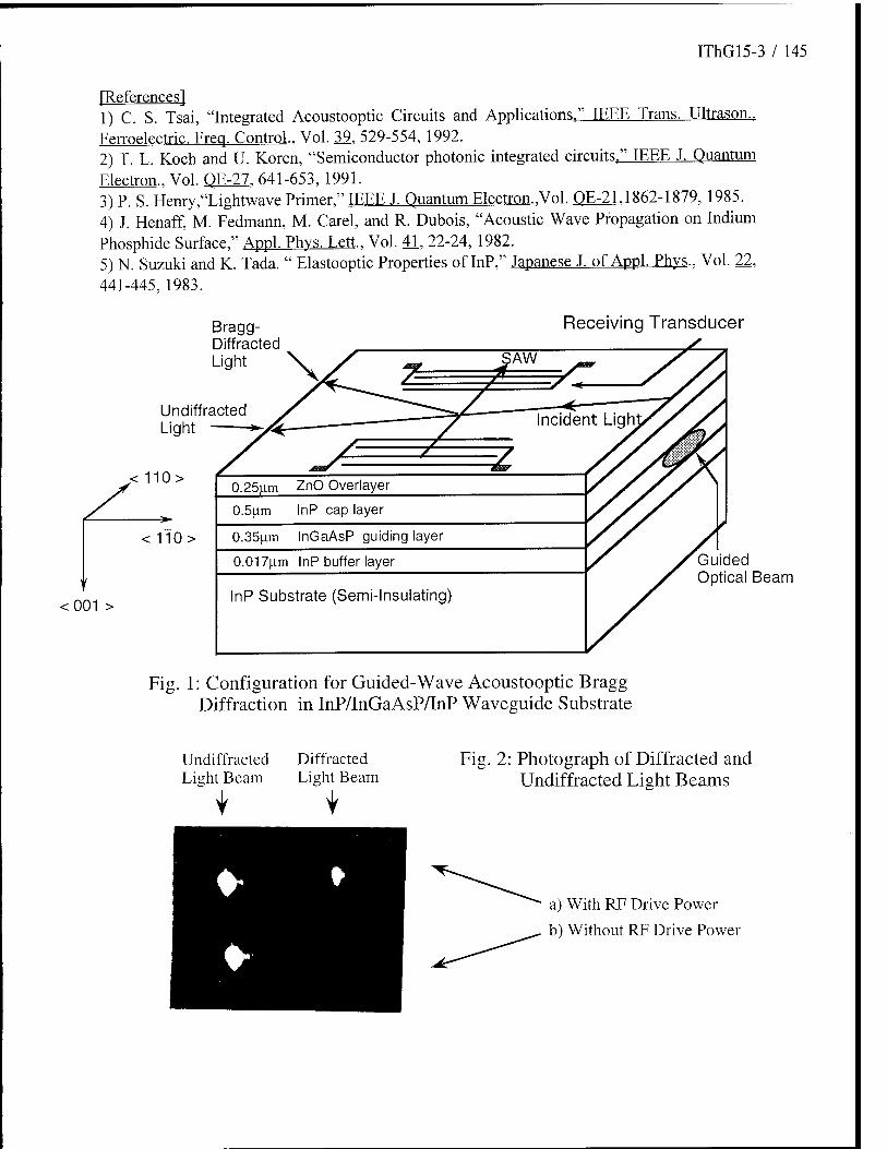
IThG15-3 / 145
[References] 1) C. S. Tsai, "Integrated Acoustooptic Circuits and Applications." TREE Trans. Uttrason., Ferroelectric. Freq. Control. Vol. 39, 529-554, 1992. 2) T. L. Koch and U. Koren, "Semiconductor photonic integrated circuits," IEEE J. Quantum Electron.. Vol. OE-27. 641-653, 1991. 3) P. S. Henry,"Lightwave Primer," IEEE J. Quantum Electron..Vol. QE-21,1862-1879, 1985. 4) J. Henaff, M. Fedmann, M. Carel, and R. Dubois, "Acoustic Wave Propagation on Indium Phosphide Surface," Appl. Phvs. Lett.. Vol. 41, 22-24, 1982. 5) N. Suzuki and K. Tada. " Elastooptic Properties of InP," Japanese J. of Appl. Phvs.. Vol. 22, 441-445, 1983.
Bragg- Diffracted Light
Undiffracted Light
< 110 >
< 110 >
Receiving Transducer
<001 >
Guided Optical Beam
Fig. 1: Configuration for Guided-Wave Acoustooptic Bragg Diffraction in InP/InGaAsP/InP Waveguide Substrate
Undiffracted Light Beam
Diffracted Light Beam
I I Fig. 2: Photograph of Diffracted and
Undiffracted Light Beams
a) With RF Drive Power
b) Without RF Drive Power
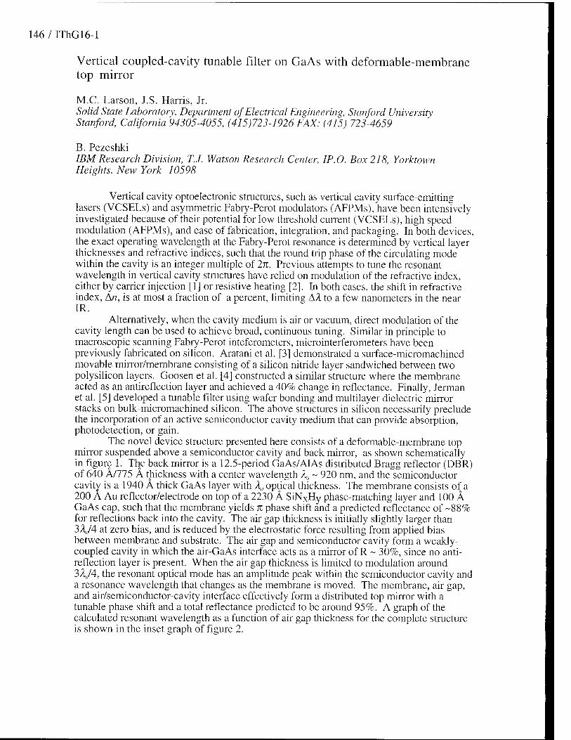
146 / IThG16-l
Vertical coupled-cavity tunable filter on GaAs with deformable-membrane top mirror
M.C. Larson, J.S. Harris, Jr. Solid State Laboratory, Department of Electrical Engineering, Stanford University Stanford, California 94305-4055, (415)723-1926 FAX: (415) 723-4659
B. Pezeshki IBM Research Division, TJ. Watson Research Center, 1P.O. Box 218, Yorktown Heights, New York 10598
Vertical cavity optoelectronic structures, such as vertical cavity surface-emitting lasers (VCSELs) and asymmetric Fabry-Perot modulators (AFPMs), have been intensively investigated because of their potential for low threshold current (VCSELs), high speed modulation (AFPMs), and ease of fabrication, integration, and packaging. In both devices, the exact operating wavelength at the Fabry-Perot resonance is determined by vertical layer thicknesses and refractive indices, such that the round trip phase of the circulating mode within the cavity is an integer multiple of 2n. Previous attempts to tune the resonant wavelength in vertical cavity structures have relied on modulation of the refractive index, either by carrier injection [1] or resistive heating [2]. In both cases, the shift in refractive index, An, is at most a fraction of a percent, limiting AA to a few nanometers in the near IR.
Alternatively, when the cavity medium is air or vacuum, direct modulation of the cavity length can be used to achieve broad, continuous tuning. Similar in principle to macroscopic scanning Fabry-Perot inteferometers, microinterferometers have been previously fabricated on silicon. Aratani et al. [3] demonstrated a surface-micromachined movable mirror/membrane consisting of a silicon nitride layer sandwiched between two polysilicon layers. Goosen et al. [4] constructed a similar structure where the membrane acted as an antireflection layer and achieved a 40% change in reflectance. Finally, Jerman et al. [5] developed a tunable filter using wafer bonding and multilayer dielectric mirror stacks on bulk-micromachined silicon. The above structures in silicon necessarily preclude the incorporation of an active semiconductor cavity medium that can provide absorption, photodetection, or gain.
The novel device structure presented here consists of a deformable-membrane top mirror suspended above a semiconductor cavity and back mirror, as shown schematically in figure 1. The back mirror is a 12.5-period GaAs/AlAs distributed Bragg reflector (DBR) of 640 A/775 A thickness with a center wavelength X0 ~ 920 nm, and the semiconductor cavity is a 1940 A thick GaAs layer with X„ optical thickness. The membrane consists of a 200 A Au reflector/electrode on top of a 2230 Ä SiNxHy phase-matching layer and 100 A GaAs cap, such that the membrane yields n phase shift and a predicted reflectance of -88% for reflections back into the cavity. The air gap thickness is initially slightly larger than 3A,/4 at zero bias, and is reduced by the electrostatic force resulting from applied bias between membrane and substrate. The air gap and semiconductor cavity form a weakly- coupled cavity in which the air-GaAs interface acts as a mirror of R ~ 30%, since no anti- reflection layer is present. When the air gap thickness is limited to modulation around 3/L/4, the resonant optical mode has an amplitude peak within the semiconductor cavity and a resonance wavelength that changes as the membrane is moved. The membrane, air gap, and air/semiconductor-cavity interface effectively form a distributed top mirror with a tunable phase shift and a total reflectance predicted to be around 95%. A graph of the calculated resonant wavelength as a function of air gap thickness for the complete structure is shown in the inset graph of figure 2.

IThG16-2 / 147
The device epitaxial layers were grown by MBE on n+ GaAs (100) substrates. An undoped 0.82 |im AlAs sacrificial layer and 100 A GaAs cap were grown on top of the GaAs cavity. This AlAs would be selectively etched away in the final processing step and corresponds to an unbiased air gap of around 3ÄJ4 + 0.15A0. After MBE growth, a 0.22 u\m thick SiNxHy layer was deposited in tensile stress by PECVD, followed by electron- beam evaporation and liftoff of Ti/Au contact pads and 200 A Au electrodes. Exposed silicon nitride was patterned by dry-etching to form membrane structures with 20 fim to 100 |im square or circular active regions and four support legs 70-100 |im in length. Finally, the AlAs sacrificial layer beneath the membranes was removed using a wet chemical etch to form the air gap. After etching, the devices were freeze-dried in tert- butanol to alleviate membrane collapse due to surface tension effects during drying [6]. Indium solder was used for the substrate electrical contact.
The devices were characterized using a tunable TkSapphire laser. Reflectivity spectra were obtained by focusing the incident beam onto the surface of the device with a 25X microscope objective. Reflectance was normalized to that of a 1000 Ä Au contact pad. The reflectance spectra for a 40 (im square device under various biases are shown in figure 2. Here the resonant mode clearly shifts from around 937 nm at 0 V bias to 905 nm at 14 V. The measured resonant wavelength and membrane displacement as a function of bias are shown in figure 3. We expect a parabolic relationship between membrane vertical displacement and applied voltage for small displacements, because the electrostatic force between the membrane and substrate can be approximated by that formed between two plates of a parallel-plate capacitor, which is of the form
F = eAV72d2 (1) where F is the attractive force between membrane and substrate, A is the area of the membrane, e is the dielectric constant, and d is the gap thickness. As shown in figure 3, the displacement is parabolic with voltage up to nearly 10% of the initial gap thickness. Using equation 1 and the voltage-displacement data from figure 3, we obtained a linear relationship between the membrane's restoring force and d, yielding an effective spring constant for the membrane of -25 N/m. This would suggest the possibility of ac modulation at frequencies of up to 100kHz.
The experimental full-width half-maximum (FWHM) linewidth of the cavity resonance as a function of wavelength is shown in figure 4. The linewidth varies from 2.5 nm near 920 nm up to approximately 3.5 nm near 937 nm, yielding a measured cavity finesse in the range of 38 to 61. Numerical simulations predict a minimum linewidth below 2.0 nm. This discrepancy might be explained by a number of factors. Membrane flatness is a possibility, although curvature arising from membrane displacement would favor excess broadening at shorter resonant wavelengths which is clearly not present. Other loss-inducing factors might be scattering from surface roughness left by the sacrificial layer etch and scattering or a lower reflectance than predicted in the Au top mirror. The linewidth will also be broadened by incident focused light that is not at normal incidence.
In conclusion, we have described results of the first deformable-membrane interferometer to our knowledge in the GaAs/AlAs-compatible materials system, with a tuning range of 32 nm and a FWHM linewidth of approximately 3 nm in the near IR. This structure is important because it utilizes a coupled air/semiconductor optical cavity, which should be amenable to incorporation with a PEN active region for the realization of a tunable wavelength-selective photodiode or a tunable laser.
This work is being supported by ARPA contract # N00014-93-1-1375 and ARPA UNM # MDA972-94-1-0003. MCL would like to acknowledge fellowship support from NSF.
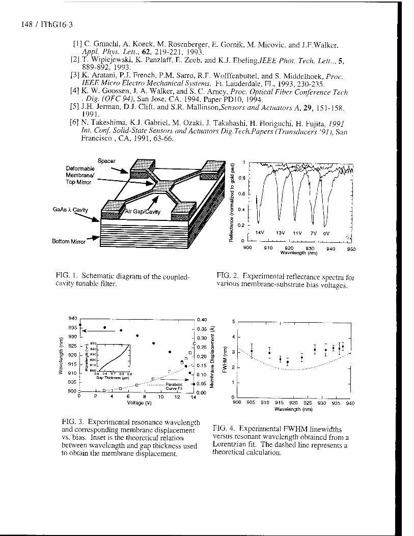
148 / IThG16-3
[1] C. Gmachl, A. Koeck, M. Rosenberger, E. Gornik, M. Micovic, and J.F.Walker, Appl. Phys. Lett., 62, 219-221, 1993.
[2] T. Wipiejewski, K. Panzlaff, E. Zeeb, and K.J. Ebeling,/E££ Phot. Tech. Lett.., 5, 889-892, 1993.
[3] K. Aratani, P.J. French, P.M. Sarro, R.F. Wolffenbuttel, and S. Middelhoek, Proc. IEEE Micro Electro Mechanical Systems, Ft. Lauderdale, FL, 1993, 230-235.
[4] K. W. Goossen, J. A. Walker, and S. C. Arney, Proc. Optical Fiber Conference Tech . Dig. (OFC 94), San Jose, CA, 1994, Paper PD10, 1994.
[5] J.H. Jerman, D.J. Clift, and S.R. Mallinson,S£>«sor<> and Actuators A, 29, 151-158 1991.
[6] N. Takeshima, K.J. Gabriel, M. Ozaki, J. Takahashi, H. Horiguchi, H. Fujita, 1991 Int. Conf. Solid-State Sensors and Actuators Dig.Tech.Papers (Transducers '91), San Francisco , CA, 1991,63-66.
Spacer Deformable Membrane/ Top Mirror
GaAs X Cavity
Bottom Mirror 900 910 920 930 940
Wavatength (nm) 950
FIG. 1. Schematic diagram of the coupled- cavity tunable filter.
FIG. 2. Experimental reflectance spectra for various membrane-substrate bias voltages.
940
935
~ 930 E -S 925
f> 920 .2 § 915 TO 5 910
905
900 6 0
BKfl
c_ 940 _ /- _ ■£ 930 ra
J 920 - > 910
- 5 900 ' ' ' ■
0.5 0.6 0.7 0.8 0.9 Gap Thickness (urn)
■ i-n-
. Parabolic Curve Fit
6 8 10 Voltage (V)
12 14
0.40
0.35 •<
0.30 §
0.25 8 .S
0.20 % Q
0.15 a> c
0.10 i
0.05 J
0.00
FIG. 3. Experimental resonance wavelength and corresponding membrane displacement
bias. Inset is the theoretical relation
5 2
T 1 1 r
N * f i l h
i i i i i
900 905 910 915 920 925 930 Wavelength (nm)
935 940
VS
between wavelength and gap thickness used to obtain the membrane displacement.
FIG. 4. Experimental FWHM linewidths versus resonant wavelength obtained from a Lorentzian fit. The dashed line represents a theoretical calculation.
IThG17-l / 149
Impedance-Mismatched Asymmetric Fabry-Perot S-SEED for Noniased Optical Bistability
Y. W. Choi, O. K. Kwon, J. H. Baek, B. Lee, and E.-H. Lee Research Department, Electronics and Telecommunications Research Institute, P. O. Box 106,
Yusong, Taejon, 305-600, KOREA (tel): +82-42-860-6026, (fax): +82-42-860-5033, (e-mail): [email protected]
Introduction: Symmetric-self-electrooptic effect device (S-SEED), consisting of two multiple quantum well (MQW) p-i-n diodes connected in series, has been one of the most promising optical bistable devices.!1] Conventional S-SEED based on quantum confined stark effect, however, requires large external reverse bias to induce sufficient electric field difference between two diodes, which inevitably entails complex metal wiring and causes increases in switching energy and ohmic heatingPl Therefore, nonbiased optical bistability (NOB) would be an attractive characteristic for fast switching speed, low switching energy, and lay-out simplification in all-optical parallel switching systems if the NOB is realized with moderate reflectivity change (AR), contrast ratio (CR) and bistability loop width (A).
Device Design and Fabrication: As has been reported, NOB can be realized in S-SEED made of extremely shallow quantum wells (ESQWs)J3] It is because the low-field electroabsorption and exciton ionization of ESQW push the maximum photocurrent (Ipm) of p-i-n diode SEED to forward bias region, that is the necessary condition for NOB in S-SEED scheme. This implies that increased photo-excited carriers due to the increased absorption contribute to photocurrent in the p-i(ESQWs)-n diode, though the electric field by the forward bias is very small. In conventional p-i(MQW)-n diode having high barriers (e.g. Alo.3Gao.7As), however, the electric field by forward bias is not sufficient for the excited photo- carriers to contribute to photocurrent resulting in Ipm at around zero voltage (+ 0.1 V) and inadequacy for NOB.
Nevertheless, the NOB in ESQW S-SEED was very small, because the intrinsic region thickness (ti) of 1 urn was too large to induce sufficient electric field difference by the built-in voltage. Recently we reported that the impedance-matched asymmetric Fabry-Perot (AFP) ESQW S-SEED (AE-SEED) with thin ti enhanced the changes of electric field and absorption coefficient (a) for the given bistable operating voltages (+V0p), thus improving NOBJ4! Though the impedance-matched AE-SEED, in which a0ffd = - 0.5 /«(Rf/Rb) for Roff to be null, showed very large CR (theoretically infinite), A and AR were relatively small (point A in Fig. 1). Here, d is the total thickness of light absorbing region. In photonic switching system, however, A and AR become the limiting factors in improving beam tolerance and bit-rate, respectively, as long as CR is sustained to be a certain value (e.g. 6:l)i5] Since A and AR are in trade-off relation with CR in normally-off AFP, an impedance-mismatched AE-SEED with decreased d for large A and AR, and reasonable CR would be appropriate for the optical systems. Furthermore, it is also expected that increased Vop with the decreased d enhances the electric field modulation for the NOB.
In this work, we designed a structure incorporating impedance-mismatched normally-off AFP and ESQWs. For the bottom mirror reflectivity (Rb) of 0.95, 14 pairs of undoped AlAs/Alo.lGao.9As (72.5/61.6 nm) quarter-wave stacks were grown on semi-insulating GaAs substrate. Then, the p- i(ESQWs)-n diode structure followed. Undoped Alo.04Gao.96As/GaAs (10.0/10.0 nm) ESQWs of 20.5 periods and two undoped 20.0 nm Alo.1Gao.9As buffers were sandwiched between P+ and N+ Al0.lGa0.9As contact layers, d of 200.0 nm was determined assuming previously reported a's of ESQW (a0ff « 16000 and don « 7000 cm"1) for the impedance-mismatch point B in Fig. 1. For the phase-matching condition of

150 / IThG17-2
the AFP, we carefully controlled the total cavity thickness from the bottom mirror to the surface mirror (air/semiconductor interface, Rf « 0.32) to be 24 time of XIA.
Fig. 2a and 2b show the fabricated AE-SEED for NOB and its circuit diagram, respectively. The mesa of the device was 140 x 180 urn2. Note that the device was fabricated by simply connecting two diodes after electrical isolation of each diode. Contrary to the conventional S-SEED array, where each S- SEED is electrically connected for external bias, AE-SEED in nonbiased optical bistable array using this lay-out can be electrically independent of each other. This implies that more densely packed and fault- tolerable optical bistable array can be easily accomplished with the nonbiased optical bistable AE-SEED in such a simple and independent lay-out.
Results and Discussions: Fig. 3 shows the NOB measured at the ESQW exciton wavelength of 856 nm. In the measurement, triangularly modulated signal beam Ps from 0 to 110 uW was incident to the one diode while a constant bias beam Pb of 50 u.W was incident to the other. The experimental power range with the focused spot diameter of about 25 u.m was low enough to be free from exciton saturation or thermal ohmic heating. The high- and low-state reflectivity, Ron and Roffwere about 23 % and 6 %, respectively, resulting in AR and CR of about 17 % and 3.7:1. A of the NOB, defined by 100 x (P2 - Pl)/Pb, was about 53 %. Here, Pi and P2 are the powers at which the transition between on- and off-state occurs. The above characteristics of NOB remained the same with the power increases up to Ps = 0 ~ 1.2 mW and Pb = 0.5 mW (our experimental limit).
Fig. 4 shows the photocurrent (solid line) measured at the operating wavelength and its load line (dotted line) in the AE-SEED geometry. It clearly shows the negative photoconductance and Ipm at forward bias that are the necessary conditions for NOB. From Fig. 4, Vop is easily ascertained to be about 0.9 V. This implies that the electric field is changed between 1.3 and 5.3 x 10⁴ V/'cm in the AE-SEED only by the p-i-n diode built-in voltage of 1.5 V. This change of field approximates to what occurs in conventional ESQWs S-SEED (ti = 1.0 um) biased at - 4 V. Note that -5 V was sufficient to induce the maximum modulation in ti = 1.0 urn ESQWs.t3l From the load line analysis, A can be expressed in another form as (A0ff2-Aon2)/AoffAon, where Aon and A0ff are the absorptances corresponding to the on- and off- states of the diode, respectively. Using calculated aon and a0ff ( aon = 17750 and a0tT= 9550 cm"1), Aon and A0fr were about 0.672 and 0.872, respectively, resulting in A of 53 %. This value is in perfect agreement with the measured value, thus verifying our experimental data and estimations of aon and a0ff.
Conclusion: Using impedance-mismatched AE-SEED, improved NOB in A and AR has been realized. A, AR, and CR of the NOB were as high as 53 %, 17 %, and 3.7:1, respectively, validly proving the improvement of the NOB. It was realized by the low-field electroabsorption and exciton lonization of ESQW and by large electric field modulation due to the large Vop (0.9 V) and thin ti (0.45 urn) of the impedance-mismatched AFP.
References I.A. L. Lentine, H. S. Hinton, D. A. B. Miller, J. E. Henry, J. E. Cunningham, J. E., and L. M. F.
Chirovsky, IEEE J. of Quantum Electron., 25, pp. 1928-1936, 1989. 2. O. K. Kwon, Y. W. Choi, K. J. Kim, and E. -H. Lee, submitted to IEEE PTL, Sept. 1994. 3. R. A. Morgan, M. T. Asom, L. M. F. Chirovsky, M. W. Focht, K. G. Glogovsky, G. D. Guth, G. J.
Przybylek, L. E. Smith, and K. W. Goossen, Appl. Phys. Lett.. 59, 1049, 1991 4. Y. W. Choi, O. K. Kwon, and E.-H. Lee, IEEE Photon. Tech. Lett., 5, 1406, 1993 5. A. L. Lentine, D. A. B. Miller, L. M. F. Chirovsky, L. A. DAsaro, IEEE J. of Quantum Electron., 27.
2431, 1991
IThG17-3 / 151
100
CR 10 i
1
0.4
0.3
AR 0.2 ■
0.1
-(b) ! m m m
/ ' \. / ' ' \
°l , \ y
/' B -A \ ■ i i
r '
1 0 0.2 0.4 0.6 0.8 1 0 0.2 0.4 0.6 0.8
cioffD a0ffD
Fig. 1. Contrast ratio and AR (=Ron -R0ff) of AFP with Rf = 0.32 (solid line) and anti-reflectionon coated conventional structure (dotted line) assuming aon/a0ff = 0.35 and Rb = 0.95. Point A and B indicated the impedance-matching and -mismatching conditions of the AFP structure, respectively.
(a) (b)
D1 D2
P. "" Pb window
p-ohmic
isolation
Fig. 2. (a) Fabricated AE-SEED for NOB in a simple lay-out. (b) Circuit diagram of (a) for NOB. When V = Vop, D1 and D2 are in low- and high-states, respectively.
-1.5
0 50 100
INPUT POWER {\i\N)
Fig.3. Measured NOB of the AE- SEED.
-260
Incident Power
= 360 uW
Fig. 4. Measured photocurrent of the p-i(ESQW)-n diode and load line in the AE-SEED geometry without external bias
152 / IThG18-l
InGaP/AlInGaP quantum well waveguide modulators for visible wavelengths
O. Blum, I. J. Fritz, R. P. Schneider, Jr., A. J. Howard Sandia National Laboratories, MS0603, Dept. 1312, Albuquerque, NM 87185-0603
Recent advances in visible wavelength semiconductor lasers (<700 nm) [1] have spurred interest in modulators operating at these wavelengths. This wavelength range is of enormous interest in the areas of plastic fiber communications, displays and optical storage. Although multiple quantum well (MQW) waveguide modulators have been successfully demonstrated in the IR wavelength range [2], development of visible MQW modulators has been severely limited by material constraints [3]. II-VI materials, such as CdZnTe/ZnTe MQWs [4] and ZnSe/ZnSSe bulk layers [5] have been used to fabricate waveguide modulators at operating at 640 nm and 488 nm, respectively. In this letter, we report a first MQW GalnP/AlGalnP waveguide modulator. Use of this material system automatically assures compatibility and integrability with the most promising visible semiconductor lasers, which also consist of GalnP/AlGalnP layers. Integration of such modulators with compatible lasers could result in much faster switching than direct modulation of the active devices, as well as chirp free operation. Switching speeds of modulators are RC limited, because they rely on field effects for operation. These switching speed can be reduced by lowering device capacitance, which depends on the device size and can be made as small as technologically viable. In contrast, lasers rely on carrier injection and therefore their switching speeds are limited by carrier lifetimes. Furthermore, modulator switching requires far less power, since no current is drawn. These two considerations make integration attractive for plastic fiber communications and displays. Our structures were grown without rotation on n+ GaAs substrates by low-pressure metal organic vapor phase epitaxy (MOVPE) using growth conditions described previously [3]. The undoped 0.5 Lim MQW active region consists of 25.5 periods of 100 A Ino.49Gao.51P wells and 100 A Ino.49(AlQ.4Gao.6)0.5lP barriers, sandwiched by a 0.2 urn p-doped Alo.8Gao.2As cladding with a p+ AlGaAs/GaAs cap layer on top , and a n-doped 0.5 urn Alo.8Gao.2As cladding on the bottom. The samples were wet etched to form 50 urn wide ridge waveguides first with a standard H3PO4: H202:H20 (1:4:45) etch to remove the GaAs cap AlGaAs cladding, followed by H3PC>4:HC1:H20 (10:5:3) etch for the phosphides for a total etch depth of 1.1 urn. The top side p contact consisted of Ti/Pt/Au stripe, while the full surface Ge/Au/Ni/Au layer contacted the substrate (n-type) side. The current-voltage characteristics were measured to ensure that desired reverse biases could be applied without much current leakage. Leakage currents of less than 100 uA were obtained for an applied voltage -10<V<+1 V. Transmission measurements were performed using a chopped argon pumped dye laser (with DCM dye) as a source and a Si detector with a lock-in. Differential transmission measurements used a programmable voltage source to apply square wave modulation to the sample, as well as to provide reference for the lock-in. Surface normal photocurrent measurements were performed on the part of the same wafer fabricated into mesa structures to obtain information about the position of the bandedge, which was determined to be at 638 nm. This agrees quite well with the calculated value of electron - heavy hole transition at 639.7 nm. All measurements were taken at room temperatures. ON:OFF ratio curves at several wavelengths for TE and TM polarizations are shown in Fig la and Fig. lb respectively. The ON state is defined as the transmission for an applied voltage of 1 V, whereas the OFF state is defined as transmission at -5.5V. These ratios were obtained from

IThG18-2 / 153
measured transmission as a function of applied reverse biases divided by OFF state transmission. As seen in Fig. la, the largest ON:OFF ratio is clearly achieved for TM polarized light at 664 nm with a measured value of 20.2 dB (106:1). For both longer and shorter wavelengths, the maximum ON:OFF ratio decreases. For TE polarized light ON:OFF ratios in excess of 15 dB are reached at 664 nm and 662 nm (Fig. lb). For longer and shorter wavelengths the ON:OFF ratio decreases. This can be better understood by noting the dependence of the differential transmission AT/T = [T(0V)-T(bias)]/T(0V), shown in Fig. 2a and Fig. 2b for TM and TE polarized light respectively. In Fig 2a, it can be seen that for TM polarized light, AT/T is the largest near 640 nm (for voltage swing from 0V to 6V) and that peak is relatively well defined. For both shorter and longer wavelengths smaller differential transmission is observed. This corresponds to the maximum ON:OFF ratio seen at that wavelength and smaller ON:OFF ratios at both shorter and longer wavelengths. It should be noted that as the value of the maximum voltage swing increases, the position of the peak of AT/T shifts toward longer wavelengths. Consequently if teh OFF state is defined at a bias larger than -5.5 V, the peak ON:OFF ratio increases and occurs at longer wavelengths. This was found to be the case when the OFF state was chosen to be -10V. Maximum ON:OFF ratio had a value of 21.6 dB (146:1) and it occurred at 667 nm. In Fig. 2b for TE polarized light, AT/T for voltage swing from 0V to 6V is also peaked near 640
nm, but the peak is much broader. It can be seen that the maximum value of AT/T for that voltage swing, is somewhat lower than the maximum value obtained for TM polarized light for the same voltage swing. One might expect a higher value for the TE polarized light, because of both the light and heavy hole contributing to the absorption, as opposed to only the light hole contribution for TM polarized light. One possible explanation may be the higher value of ON state absorption for the TE polarization (and thus lower ON state transmission), since the heavy hole contribution occurs at longer wavelengths than the light hole. Thus below the bandedge, where the modulator operates, residual absorption from the heavy hole affects the ON state transmission for the TE polarization. The width of the AT/T peak accounts for the maximum ON:OFF ratio occurring at 662 nm and 664 nm. Increasing the voltage swing broadens the peak position of AT/T and shifts it toward longer wavelengths, but not as dramatically as for the TM polarized light. The difference between the maximum ON:OFF ratio for 664 nm and longer wavelengths decreases, but the largest ON:OFF ratio is still obtained at 664 nm. If the OFF state is chosen at -10V, the maximum ON:OFF ratio, occuring at 664 nm is 18.4 dB (66:1), whereas at 667 nm it is 17.4 dB (54:1). In conclusion, we have demonstrated the first waveguide modulator utilizing MQWs in InGaP/ÄlInGaP. The voltage swing of 0V to -5.5V results in modulation with ON:OFF ratio in excess of 20 dB at 664 nm for TM polarized light.
[1] see special issue of IEEE J. Quantum Electron., June 1993 [2] R. H. Ran, R. J. Simes, L. A. Coldren; IEEE Photon. Technol. Lett, 1, 1989, pp. 273-275 [3] I. J. Fritz, O. Blum, R. P. Schneider, Jr., A. J. Howard and D. M. Follstaedt; Appl. Phys, Lett.,
64, pp. 1824-1826 [4] D. Lee, J. E. Zucker, M. D. Divino, R. F. Austin, R. D. Feldman, K. L. Jones and A. M.
Johnson; App. Phys. Lett., 59, 1991, pp. 1867-1869 [5] M. H. Jupina, E. M. Garmire, N. Shibata and S. Zembutsu; Appl. Phys. Lett., 57,990, pp.
2894-2896
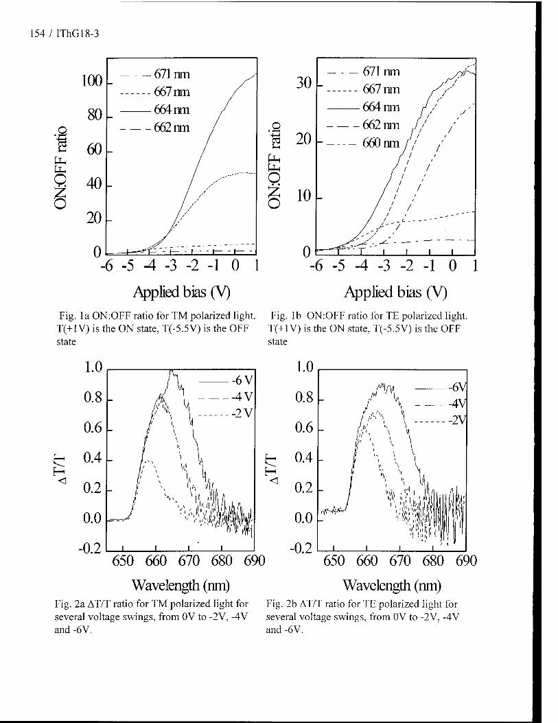
154 / IThG18-3
100
80 Q
S 60
2 40 6
20
671 nm 667 nm 664 nm 662 ran
0
30-
.9 'S 20 5—(
0
— - — 671 nm vC - -- 667 nm / /
/
— 664 nm r / / / J I y'
-662nm [ 1 I I
1 /' - 660nm//
/ / / /
/ / / / / / / /
1 1
1
i i
— / /
/ ' ' - "
A-/"?" -^r'l ^1 . — - — - —
_—=f^ '- r" i i i i
-6 -5 -4-3-2-10 1
Applied bias (V)
_6 -5 -4 -3 -2-10 1
Applied bias (V) Fig. la ON:OFF ratio for TM polarized light. Fig. lb ON:OFF ratio for TE polarized light. T(+l V) is the ON state, T(-5.5V) is the OFF T(+l V) is the ON state, T(-5.5V) is the OFF state state
650 660 670 680 690
Wavelength (nm)
650 660 670 680 690
Wavelength (nm) Fig. 2a AT/T ratio for TM polarized light for Fig. 2b AT/T ratio for TE polarized light for several voltage swings, from 0V to -2V, -4V several voltage swings, from 0V to -2V, -4V and -6V. and -6V.

IThG19-l / 155
Paper Withdrawn

156 / IThG20-l
Compact Waveguide Polarization Beam Splitter
using a Multimode Interference Coupler
H. Okayama and M. Kawahara
R&D Group, Oki Electric Industry Co., Ltd.
550-5 Higashiasakawa, Hachioji, Tokyo, 193 Japan
Introduction
The polarization beam splitter is often used in composing a polarization-independent
wavelength filter employing mode conversion. The length of the polarization beam splitter
should be short as possible to allocate sufficient length for the wavelength filter and to render the
device integratable on a substrate having a limited area. The most compact device demonstrated
thus far uses intersecting waveguides [1], but the fan out waveguides needed to connect the
device to the mode converter required a certain length. This report demonstrates a device shorter
than 1 mm which requires no fan out waveguides.
Device structure
Figure 1 shows a schematic structure of the device. Two parallel waveguides are placed apart,
and a rectangular birefringent section is formed between them. The LiNb03 waveguide is
fabricated using Ti indiffusion and the birefringent section is fabricated using proton exchange.
The refractive index for ordinary light is decreased by proton exchange (Fig. 2(A)). The parallel
waveguides are isolated for ordinary light and the bar state is achieved. The refractive index of
extraordinary light is enhanced by the proton exchange (Fig2(B)). A waveguide is formed for the
extraordinary light between the parallel waveguides in the birefringent section. The parallel
waveguide and the birefringent section together form a multimode interference coupler [2].
Properly setting the refractive index for the birefringent section enables the cross state to be
established for the extraordinary light. The input and the output ports are connected in the cross
direction for the extraordinary light. We need not pay much attention in fabrication conditions
about TE mode, which makes the device easier to fabricate than the conventional device.
Device operation can also be explained by using normal modes in the multimode interference
coupler. Due to the different refractive index profile, different normal modes are excited for the
TM and TE modes. For the TM mode, the excited normal modes are those whose spatial period
are near the width of the input light field. Modes from the 3rd to 7th order, for example, are
excited in the structure that will be described in the experiment. These modes are almost in

IThG20-2 / 157
synchronization and by setting the proper length for the coupler, the phase between symmetric
and asymmetric normal modes is flipped at the ouput port, thus achieving the cross state. For the
TE mode, the excited normal modes are 1st and 2nd order modes with degenerated propagation
constants. The normal modes are the same for those in the two weakly coupled waveguides, thus
attaining the bar state [2].
Experiment and results
X-cut LiNb03 is used as a a substrate, which is often chosen for fabricating wavelength filters
employing a mode conversion. The parallel waveguides were formed by indiffusing 10-u.m
wide, and 90-nm thick Ti stripe patterns separated by 30 um. Ti diffusion was conducted at a
temperature of 1050° C for 8 hours. The birefringent section is 1 mm long and 20 Jim wide
rectangular region fabricated by using proton exchange. The proton exchange followed by an
annealing process was done at 200°C for 1.5 hours after the Ti diffusion.
The characteristics of the device were measured using an external cavity tunable laser diode
emitting light at a wavelength of about 1.3 |im. The best extinction was achieved at 1.335 |im.
The extinction ratio was 30 dB for the TM mode and 29 dB for the TE mode. The extinction ratio
for the TM mode exceeded 20 dB in the wavelength ranging from 1.33 |im to 1.34 Jim. The
extinction ration for the TE mode exceeded 24 dB at all the measured wavelength ranging from
1.32 |im to 1.35 u.m. The results of a simulation using beam propagation method show that with
proper refractive index setting, the extinction ratio for the TM mode would exceed 15 dB for
much wider wavelength range covering both 1.3 \im and 1.55 u.m wavelengths.
Conclusion We demonstrated a compact waveguide polarization beam splitter with a high extinction ratio
fabricated on a x-cut LiNb03 substrate. The structure based on a multimode interference coupler,
requires no fanout waveguides. An 1 mm long device attained an extinction ratio of 30 dB.
References
[1] T. Pohlmann et al., IEEE J. Quantum Electron., vol. 27, p. 602, 1991.
[2] H. Okayama et al., presented at OEC'94, paper 15B3-6.
158 / IThG20-3
r birefringent region
(proton-exchanged region)
. A Ti-indiffused waveguide
TM
TE
^zr
multimode interference coupler
Fig. 1 Structure of the polarization beam splitter employing a multimode interference coupler.
x CD
CD >
A
ordinary light (TM)
-► Z
X CD
"Ö c CD >
O CO L.
vj—
CD C_
A
extraordinary light (TE)
A'
-► Z
Fig. 2 Refractive index distribution for the multimode interference coupler including a birefringent region.

IThG21-l / 159
Novel Broad Band Excitation of Pr^+ Luminescence in Pr:Asi2Ge33Se55 Glasses
S.Q. Gu, D.A. Turnbull, S. Ramachandran, E.E. Reuter, J.T. Verdeyen, and S.G. Bishop
Engineering Research Center for Compound Semiconductor Microelectronics Department of Electrical and Computer Engineering, University of Illinois at Urbana
Urbana,IL 61801
Tel# 217-244-6378 Fax# 217-244-6375
Chalcogenide glasses have unique properties which may lead to low cost integrated photonic devices. The ability to modify their refractive index by photodarkening enables chalcogenide glasses to be patterned for passive and active waveguide device applications. In particular, rare earth doped chalcogenide glasses are attractive for planar waveguide devices operating in the 1300 and 1550 nm range because of the ability to pattern waveguides by photodarkening, infrared transparency, high refractive index, low phonon energies, and ease of thin film deposition.
Our previous photoluminescence (PL) studiesl>2>3 of Er3+ doped AS2S3 and Ge33Asi2Se55 glasses demonstrated that Er^+ is incorporated into optically active sites in the glass and gives rise to two broad emission bands: -980 nm (^II 1/2—>^I 15/2) and -1550 nm
0*Il3/2—>^Il5/2)- The 1550 nm PL spectrum has lineshape similar to that observed in Er-doped oxide glasses but with a larger half width. For the 1550 nm emission band, the PL excitation (PLE) spectra in Er-doped chalcogenide glasses exhibit a remarkably broad excitation band which extends from -500 nm to beyond 1000 nm, in addition to the expected 810 nm (^115/2—^19/2) and 980 nm (^"113/2—>^"115/2) Er3+ PLE bands. We attribute these broad PLE bands to below-gap defect states which efficiently transfer energy to Er3+ in Er doped chalcogenide glasses.
In this paper, we present a parallel investigation of the optical properties of Pr3+ doped Ge33Asi2Se55 glasses. The results demonstrate that the unusual, broad-band PLE mechanism discussed above is not unique to Er-doped chalcogenide glasses. Bulk samples of 0.2 wt.% Pr^+ doped chalcogenide glass were prepared from a mixture of Ge33Asi2Se55 glass and crystalline Pr2S3. The mixture was sealed in a quartz ampoule, heated to 1000° C, and cooled to room temperature. The Pr:Ge33Asi2Se55 sample was investigated by PL and PLE spectroscopies with temperature ranging from 5 to 300 K.
When the 0.2 wt % Pr:Ge33Asi2Se55 sample is excited at -1040 nm (3H4^1G4), the PL spectrum exhibits two broad bands peaked at 1340 nm (IG4—»3H5) and 1620 nm (3F3—PH4), as shown in Fig. 1. The lineshape of the 1340 nm PL band is almost identical to that observed^ in PnGaLaS glasses. The fluorescence decay lifetime of the 1340 nm emission in the sample was -250 |is, which is also similar to the values in the PnGaLaS system with comparable Pr concentration^. For the 1620 nm emission band, the 0.2 wt % Pr:Ge33Asi2Se55 sample exhibits
a broad PLE band from 500 nm to beyond 1000 nm in addition to the 1040 nm (^ILi—>lG4) excitation band (see Fig. 2). This band behaved almost identically to the PLE band of the 1540 nm emission in Er:Ge33Asi2Se55.
As in Er:Ge33Asi2Se55, the broad excitation band in Pr:Ge33Asi2Se55 may also be due to below gap states, which transfer energy from the broad absorption to Pr3+. The excitation band

160 / IThG2l-2
peaked at -700 nm can efficiently excite the emission at 1620 nm (3F3->3H4) and is stronger than
the excitation band at -1040 nm (3
H4-H>'G4). However, this extrinsic excitation band excites the
1340 nm ('G4->3H5) emission very poorly, as shown in Fig.2. This is similar to the observation in Er:Ge33Asi2Se55 where the broad band excitation excites the 1540 nm emission more efficiently than the 980 nm emission. These results suggest that the excited below gap defect states excite the rare earth ions more readily to their lower energy excited states than to their higher energy excited states.
The PLE spectra for 1620 nm emission of the 0.2 wt % Pr:Ge33Asi2Sc55 sample and 1540 nm emission of the 0.2 wt % Er:Ge33Asi2Se55 sample are compared on a semilogarithmic scale in fig. 3. Both spectra exhibit an exponential decrease in the broadband PLE intensity with decreasing exciting photon energy in the spectral range below the -1.7 eV energy gap of Ge33Asi2Se55 glass. This decrease suggests a weak, extrinsic, exponential absorption contributing to rare earth ion emission. For photon energies above the glass band gap, the broad- band PLE intensities decrease exponentially with increasing exciting photon energy due to competing nonradiative decay mechanisms. Although the exponentially decreasing slope of the two broad-band PLE spectra differ slightly for the two dopants, the slope of the decreasing high energy PLE is approximately equal to the difference between the slope of the Urbach edge and the slope of the low energy PLE tail. This suggests that the broad-band excitation is dominated by properties of the host chalcogenide glasses.
1: S.Q. Gu, Q. Xu, S. Ramchandran, E.E. Reuter, J.T. Verdeyen, and S.G. Bishop, Proc. of 1994 Conf. on Laser and Electro-optics, p.336.
2: S.Q. Gu, S. Ramachandran, E.E. Reuter, D.A. Turnbull, J.T. Verdeyen, and S.G. Bishop, "Photoluminescence and Excitation Spectroscopy in Er:As2S3 Glass: Novel Broad Band Excitation Mechanism", to be published.
3: S.Q. Gu, D.A. Turnbull, S. Ramachandran, E.E. Reuter, J.T. Verdeyen, and S.G. Bishop, "Novel Broad Band Excitation of Er3+ Emission in Chalcogenide Glasses", to be published.
4: K. Wei, D.P. Machewirth, J. Wenzel, E. Snitzer, and G.H. Sigel, Jr., to be published.

IThG21-3 / 161
c
<
c CD
■+-» c
1200 1400 1600 Wavelength (nm)
Fig. 1 PL spectrum of the 0.2 wt % Pr:Ge33Asi2Se55 at 300 K excited at 990 nm.
co +^ 'c
CD
CO c CD
—rr~ ' \ / i i i ' i
T" T
\r~"~
PLE detected at 1340 nm 1620 nm
600 800 1000 Wavelength (nm)
Fig. 2 PLE spectra of the 0.2 wt % Pr:Ge33Asi2Se55 at 300 K at detection PL wavelength of 1340 and 1620 nm.
1 FT
'E
si <
1- 10 E
c -2 «10 c
CL-
IO
-0.2 wt% EnAsGeSe @1540nm
-0.2 wt% Pr:AsGeSe @1620nm
1 j_ _i_
1200 1600 2000 2400 Excitation Energy (meV)
Fig. 3 Semilogarithmic PLE intensity vs excitation energy at 300 K obtained from 1540 nm emission of 0.2 wt % Er:Ge33Asi2Se55 and 1620 nm emission of 0.2 wt % Pr:Ge33Asi2Se55.
162 / IThG22-l
Material Assessment of Aerosol Doped Neodymium Silica Waveguide
Lasers
J. R. Bonar, J. A. Bebbington, and J. S. Aitchison,
University of Glasgow,
Department of Electronics and Electrical Engineering,
Glasgow, G12 8QQ, U.K..
Telephone: +44 41 339 8855 Facsimile: +44 41 330 4907
e-mail: [email protected]
Silica-based integrated optical waveguides are receiving increasing attention for applications in future optical communication systems. Based on a combination of silica film deposition and reactive ion etching (RIE), the resulting channel waveguides have a low loss, precisely defined core structure and a low waveguide to fibre coupling loss due to the core dimensions and refractive index matching those of silica-based optical fibres. Of the several silica deposition techniques, flame hydrolysis deposition (FHD) offers the greatest flexibility and gives the possibility of monolithic integration of active and passive functions on a single substrate [ 1, 2 ].
Active planar silica waveguides are formed by doping with rare earth ions using either the solution [ 3 ] or aerosol [ 4 ] doping techniques. Both techniques have been studied and will compare the different results. To fabricate efficient rare earth doped oscillators it is necessary for the dopant to be homogeneously distributed minimising both scatter losses [ 5 ] and ion- ion interactions [ 6 ]. To this end the two techniques are compared and conditions given for increased device performance.
Scatter losses were investigated by prism coupling TE polarised light from a 4.8 mW He-Ne 632.8 nm laser into the planar films. Losses were determined as a function of thermal treatment and found to reduce as the temperature increased and the duration of the initial thermal processing decreased. The losses were found to be less dependent of subsequent thermal processing steps.
Fluorescence lifetime measurements were made on samples produced using ErCl3 solutions of 0.5 M, 1.0 M and 1.0 M co-doped with 0.4 M A1(N03)3. These gave doping concentrations of -0.1 wt % and 0.21 wt % for Nd and 0.04 wt % for Al. Differentials of the natural logarithm were measured to highlight any small departures from an exponential decay and thus indicate the presence of ion-ion interactions. A typical measurement is shown in figure 1. The slow decay component from the dispersed Er ions was typically 5 ms whilst the fast decay component became more pronounced for increased doping level, due to the ions being more susceptible to micro-clustering. The sample co-doped with Al reported the best fast decay component, due to the co-ordination of more non-bridging oxygen ions which screen the Er ions from their large cationic field strengths

IThG22-2 / 163
5.00E+02
O.OOE+00
r ^ -5.00E+02
(> 1)
T3
a -l.OOE+03 n a -1.50E+03 i)
a -2.00E+03
-2.50E+03
-3.00E+03
few , i ■1 1 i Li iii K d 1 A 1
* 1 wmmmmmMmmL -r
, . ' ! 1 ' n> 1
I (
f
V
0.0 ■ 0.2 0.4 0.6 0.8 1.0 1.2 1.4 1.6 1.8 2.0
Time (milliseconds)
Figure 1 Differential of the natural logarithm decay for 1.0 M Er sample
Having developed a process which produced low scattering losses and reduced ion-ion interactions, aerosol doped Nd samples co-doped with Al were fabricated. A CHF3 low
pressure etch was used to form 25 x 7 \mfi ridge waveguides. The channels were then over grown with a low index boron doped silica cladding glass. The waveguides were finally sawn to a length of 4.5 cm.
A laser cavity was formed by butting dielectric coated mirrors to the end of the waveguides. The device exhibited a threshold of 22 mW and a slope efficiency of 2.5 %. An example of the lasing spectrum is shown in figure 2. Similar solution doped Nd waveguides were also fabricated. A threshold of 20 mW and a slope efficiency of 2.6 % were measured for these devices.
4-
c
-4—» •1—I
X> 1-1 a
c
1.046 1.048 1.051 1.053 1.056
Figure 2 Output spectrum of an aerosol doped Nd waveguide laser

164 / IThG22-3
The initial measurements indicate that both doping regimes produce similar results, however, aerosol doping is a single step process and lends itself nicely to selective vertical and regional area doping. Results will also be presented for selective area doping using the solution doping process.
In conclusion measurements will be presented for both aerosol and solution doped Nd waveguide lasers. Conditions and material parameters will be highlighted for optimised devices. Selective area doping will also be detailed and the possibilities for integration of active and passive components discussed.
The authors would like to thank K. Piechowiak for the sawing of the waveguides, Dr G. D. Maxwell and B. J. Ainslie for helpful discussions. The work has been supported under the DTI/EPSRC, LINK programme.
References
[ 1 ] Hattori K., Kitagawa T., Ohmori Y. and Kobayashi M.: 'Laser-Diode Pumping of Waveguide Laser Based on Nd-Doped Silica Planar Lightwave Circuit', IEEE Photonics Technology Letters, 1991, Vol.3, No. 10, p.p. 882-884
[ 2 ] Hattori K., Kitagawa T., M. Oguma, Ohmori Y. and Horiguchi ML: 'Erbium-Doped Silica-Based Waveguide Amplifier Integrated with a 980/ 1530 nm WDM Coupler', Electronics Letters, 1994, Vol.30, No. 11, p.p. 856-857
[ 3 ] Bonar J. R., Bebbington J. A., Aitchison J. S., Maxwell G. D. and Ainslie B. J.: Low Threshold Nd-Doped Silica Planar Waveguide Laser', Electronics Letters, 1994, Vol.30, No. 3, p.p. 229-230
[ 4 ] Bebbington J. A., Barbarossa G., Bonar J. R. and Aitchison J. S.: 'Rare Earth Doped Silica Waveguides On Si Fabricated by Flame Hydrolysis Deposition and Aerosol Doping', Applied Physics Letters, 1993, Vol.62, No. 4, p.p. 337-339
[ 5 ] Kitagawa T., Hattori K, Hibino Y. and Ohmori Y.: 'Neodymium-Doped Silica-Based Planar Waveguide Lasers', Journal Of Lightwave Technology, 1994, Vol. 12, No. 3, p.p. 436- 442 [ 6 ] Wyatt R.: 'Spectroscopy Of Rare Earth Doped Fibres', SPIE, 1989, Vol.1171 ,.p.p 54
IThG23-l / 165
Low Loss Passive Polarisation Splitter on InP/InGaAsP by use of Mode Conversion
J0rgen W. Pedersen, Jos J.G.M. van der Tol, Ed G. Metaal Royal PTT Nederland N.V., PTT Research, Leidschendam, The Netherlands,
tel +31 70 332 3642, fax +31 70 332 6477
Y. Siang Oei, Department of Electrical Engineering, Delft University of Technology, The Netherlands,
tel +31 15 782438, fax +31 15 784046
Fokke H. Groen, Department of Applied Physics, Delft University of Technology, The Netherlands,
tel +31 15 784456, fax +31 15 783251
Ingrid Moerman, Department of Information Technology, University of Gent-IMEC, Belgium,
tel +32 9 2643334, fax +32 9 2643593
1 INTRODUCTION Integrated optical polarisation splitters are important devices in optical communication, e.g., in coherent optical detection schemes [1]. Polarisation splitters based on various materials are described in literature [2-6]. In this paper we present a polarisation splitter realised on a conventional DH InGaAsP/InP structure. Compared with a former design of the mode converting polarisation splitter [7], this device has larger polarisation splitting ratio and lower excess losses. The device based on ridge waveguides is easy to fabricate; only one etching step is required. Furthermore, this device has the advantage that no metallic layer is required [3, 5]. Finally, the fabrication tolerances of this device are relaxed compared with the classical type of polarization splitters based on interference.
2 CONCEPT The device, shown in Fig. 1, makes use of mode conversion and successive mode filtering.
TM - polariza lion
^'^™ ■ J»^
„TEOO, TMO^
TE- polar iiatioo
Input waveguide .Taper, Converting section ' Taper ,TMI- . Mode filter ■ Output waveguides . t • section ' '
Fig. 1: Schematic view of polarisation splitting device (top view).
Light (TE- and TM-polarisation) is fed with a monomode waveguide through a taper to a bimodal waveguide. TM-polarisation is converted from the 0th to the 1st order waveguide mode. This is achieved by introducing lateral offsets alternately for a fixed increase in the length (block length) of the waveguide. This block length corresponds to the half-beatlength of the 0th and 1st order waveguide modes for TM polarisation. By choosing appropriate offsets the zero111 order mode for TM polarisation is completely converted to its first order mode after a certain number of junctions. The TE polarisation is not converted due to a phase mismatch. Finally, by using a coupler selective to mode order, an adiabatic asymmetrical Y-junction [8] , polarisations are separated. The Two Mode Interference (TMI)-section is used to determine the ratio of power in the different waveguide modes and the quality of the modefilter.
166 / IThG23-2
2 DESIGN AND FABRICATION
The device operates at a wavelength of 1.5 pm. The devices are fabricated in a DH InGaAsP/InP MOVPE layer structure. The InP-cover layer thickness is 500 nm and the Q-film layer thickness is 460 nm. The bandgap of the guiding layer is 1.3 nm. The photoresist etch mask is defined using contact UV exposure. The ridge waveguide structures are etched by CH4/H2-RIE. The ridge height is 250 nm. The monomode input waveguide has a width of 3.2 pm, the taper angle is 0.25° and the width of the bimodal converter section is 6.0 pm.
The block length A is found by: A = 7t/(ß0-ßi), where ß0 and ß2 are the propagation constants for the zerom
and first order mode for TM-polarisation. The propagation constants are found by the effective index method (EM). This results in a block length A equal to 196 urn. From coupled mode theory, the conversion of modes, expressed as the normalised coupled power pc, is given by:
Vc=rr^ ^sin^N ^2+0.25S2Y (1)
where N is the number of junctions, c the mode conversion in terms of amplitude per junction and 8 the phase mismatch between the modes per block length. A = 196 pm results in 8 = 0 rad for TM- and 8 = 1.04 rad for TE-polarisation. Using these parameters and Eq. (1), an offset of 0.270 pm is found appropriate. The mode conversion per junction in terms of amplitude, c = 0.0873, was found by calculating the overlap integral between the mode profile at both sides of the junction. It is found by Eq. (1) that for N = 18 the normalised power is minimum for the TEQI and TMQQ modes and large for the TE00 and TM01 modes. The predicted excess loss is below 1 dB. The results of the simulations for N=18 are summarised in Table 1.
Table 1: Simulated normalised fraction of power in the zerom and first order polarization when using N=18 and Ax=0.270 urn.
mode for TE- and TM-
zero order modes first order mode pol. splitting [dBl excess loss [dB] TM-polarization 0.0015 0.8277 27.4 0.81 TE-polarization 0.9914 0.0000568 42.4 0.04
The number of junctions and the block length are varied in order to investigate this device as a function of N and 8. The width of the TMI-section is 5.2 11m. The length of the TMI-section is varied from 0 pm to 600 pm in steps of 100 pm. The asymmetrical Y-junction is designed to suppress the unwanted mode more than 20 dB [9]. The stem width is 5.2 urn, the narrow branch 2.0 urn and the broad branch 3.2um. The opening angle is increased from 0.28° to 0.63° after a distance of 1178 urn. The output waveguides are 3.2 pm wide having a pitch of 25 pm. This design results in a polarisation splitter of less than 7 mm long.
3 RESULTS The polarisation splitters are characterised by transmission measurements using a FP-laser at a wavelength of 1.5 pm. Optimum polarisation splitting is found for a block-length of 200 pm and 18 junctions. The splitting ratio is found by comparing the fractional output power of the narrow Y-branch with the total output power of both channels, for TE- and TM-polarisation respectively. The fractional power is given as function of TMI- section length in Fig. 2. Due to a defect, the polarisation splitter having a TMI-lengfh of 200 pm was omitted from the analysis. The polarisation splitting is found from the mean value of the fractional power. All six splitters show polarisation splitting, 13 dB for TE- and 19.9 dB for TM-polarisation. (see Fig. 2). The splitter with the best performance (TMHength 600 pm) for both polarisations shows simultaneously a splitting ratio of 17.3 dB for TE- and 21.4 dB for TM-polarisation.
The measured polarisation splitting is less than predicted by simulations. Primarily, this is due to radiation modes caused by the lateral offsets. Secondly, especially for TE-polarisation the calculated half-beatlength slighüy deviates from the experimental one. As a consequence, the TEQI mode does not have its minimum for
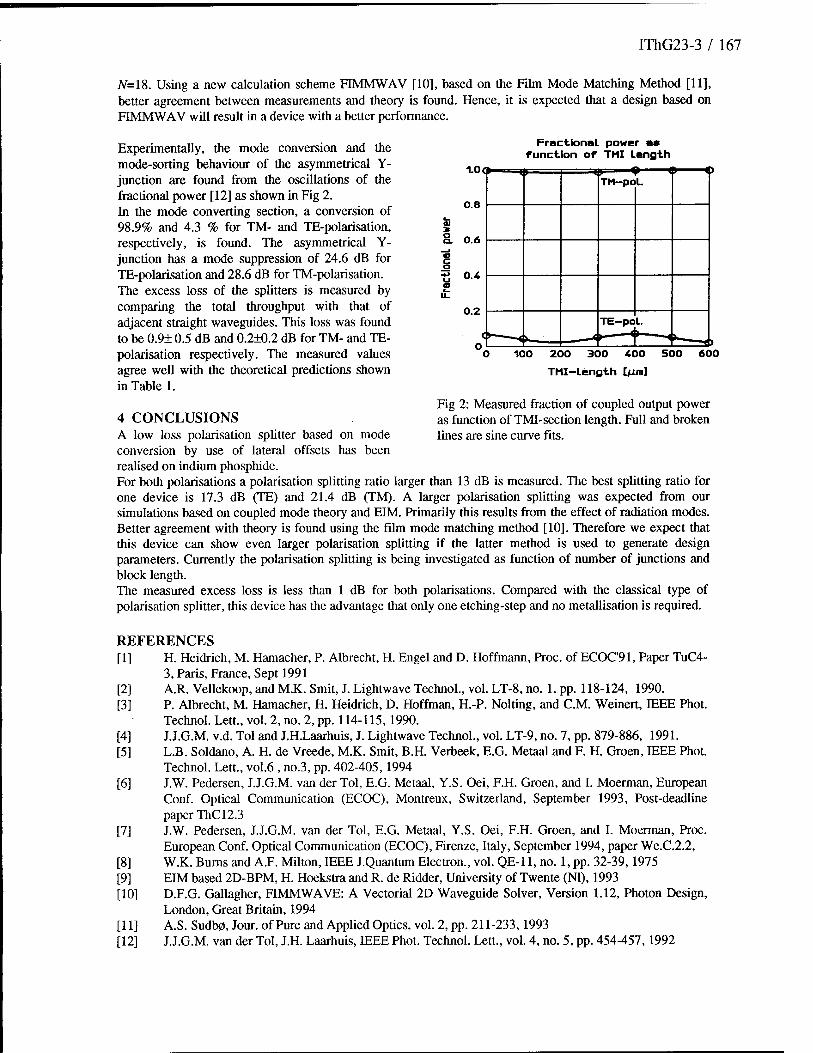
IThG23-3 / 167
N=IS. Using a new calculation scheme FIMMWAV [10], based on the Film Mode Matching Method [11], better agreement between measurements and theory is found. Hence, it is expected that a design based on FIMMWAV will result in a device with a better performance.
Experimentally, the mode conversion and the mode-sorting behaviour of the asymmetrical Y- junction are found from the oscillations of the fractional power [12] as shown in Fig 2. In the mode converting section, a conversion of 98.9% and 4.3 % for TM- and TE-polarisation, respectively, is found. The asymmetrical Y- junction has a mode suppression of 24.6 dB for TE-polarisation and 28.6 dB for TM-polarisation. The excess loss of the splitters is measured by comparing the total throughput with that of adjacent straight waveguides. This loss was found to be 0.9± 0.5 dB and 0.2±0.2 dB for TM- and TE- polarisation respectively. The measured values agree well with the theoretical predictions shown in Table 1.
S o
Fractional function of
power as TMI Length
0.8
0.6
TM-poL.
0.4
0.2 TE-poL
100 200 300 400
TMI-Length [Mm]
500 600
Fig 2: Measured fraction of coupled output power as function of TMI-section length. Full and broken lines are sine curve fits.
4 CONCLUSIONS A low loss polarisation splitter based on mode conversion by use of lateral offsets has been realised on indium phosphide. For both polarisations a polarisation splitting ratio larger than 13 dB is measured. The best splitting ratio for one device is 17.3 dB (TE) and 21.4 dB (TM). A larger polarisation splitting was expected from our simulations based on coupled mode theory and EIM. Primarily this results from the effect of radiation modes. Better agreement with theory is found using the film mode matching method [10]. Therefore we expect that this device can show even larger polarisation splitting if the latter method is used to generate design parameters. Currently the polarisation splitting is being investigated as function of number of junctions and block length. The measured excess loss is less than 1 dB for both polarisations. Compared with the classical type of polarisation splitter, this device has the advantage that only one etching-step and no metallisation is required.
REFERENCES [1]
[2] [3]
[4] [5]
[6]
[7]
[8] [9] [10]
[11] [12]
H. Heidrich, M. Hamacher, P. Albrecht, H. Engel and D. Hoffmann, Proc. of ECOC'91, Paper TuC4- 3, Paris, France, Sept 1991 A.R. Vellekoop, and M.K. Smit, J. Lightwave Technol., vol. LT-8, no. 1, pp. 118-124, 1990. P. Albrecht, M. Hamacher, H. Heidrich, D. Hoffman, H.-P. Nolting, and CM. Weinert, IEEE Phot. Technol. Lett., vol. 2, no. 2, pp. 114-115,1990. J.J.G.M. v.d. Tol and J.HLaarhuis, J. Lightwave Technol., vol. LT-9, no. 7, pp. 879-886, 1991. L.B. Soldano, A. H. de Vreede, M.K. Smit, B.H. Verbeek, E.G. Metaal and F. H. Groen, IEEE Phot. Technol. Lett., vol.6 , no.3, pp. 402-405, 1994 J.W. Pedersen, J.J.G.M. van der Tol, E.G. Metaal, Y.S. Oei, F.H. Groen, and I. Moerman, European Conf. Optical Communication (ECOC), Montreux, Switzerland, September 1993, Post-deadline paper ThC 12.3 J.W. Pedersen, J.J.G.M. van der Tol, E.G. Metaal, Y.S. Oei, F.H. Groen, and I. Moerman, Proc. European Conf. Optical Communication (ECOC), Firenze, Italy, September 1994, paper We.C.2.2, W.K. Burns and A.F. Milton, IEEE J.Quantum Electron., vol. QE-11, no. 1, pp. 32-39,1975 EIM based 2D-BPM, H. Hoekstra and R. de Ridder, University of Twente (Nl), 1993 D.F.G. Gallagher, FIMMWAVE: A Vectorial 2D Waveguide Solver, Version 1.12, Photon Design, London, Great Britain, 1994 A.S. Sudb0, Jour, of Pure and Applied Optics, vol. 2, pp. 211-233, 1993 J.J.G.M. van der Tol, J.H. Laarhuis, IEEE Phot. Technol. Lett., vol. 4, no. 5, pp. 454-457,1992
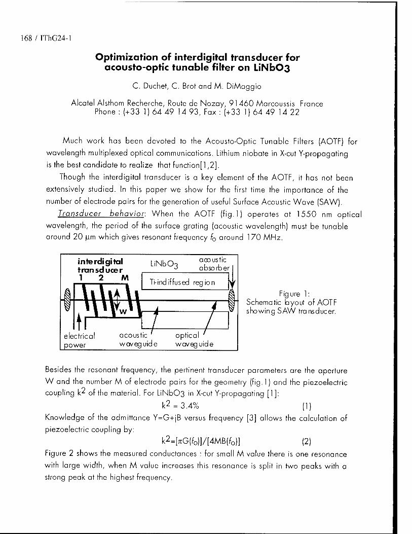
168 / IThG24-l
Optimization of interdigital transducer for acousto-optic tunable filter on LiNbOß
C. Duchet, C. Brot and M. DiMaggio
Alcatel Alsthom Recherche, Route de Nozay, 91460 Marcoussis France Phone : (+33 1) 64 49 14 93, Fax : (+33 1) 64 49 14 22
Much work has been devoted to the Acousto-Optic Tunable Filters (AOTF) for
wavelength multiplexed optical communications. Lithium niobate in X-cut Y-propagating
is the best candidate to realize that function[1,2].
Though the interdigital transducer is a key element of the AOTF, it has not been
extensively studied. In this paper we show for the first time the importance of the
number of electrode pairs for the generation of useful Surface Acoustic Wave (SAW).
Transducer behavior: When the AOTF (fig.l) operates at 1550 nm optical
wavelength, the period of the surface grating (acoustic wavelength) must be tunable
around 20 |im which gives resonant frequency f0 around 170 MHz.
interdigital transducer 1 2 M
LiNb03 acoustic absorber
electric a power
Ti-ind if fused region
t acoustic ' optical waveguide waveguide
Figure 1: Schematic layout of AOTF showing SAW transducer.
Besides the resonant frequency, the pertinent transducer parameters are the aperture
W and the number M of electrode pairs for the geometry (fig.l) and the piezoelectric
coupling k2 of the material. For LiNb03 in X-cut Y-propagating [1]:
k2 = 3.4% (1)
Knowledge of the admittance Y=G+jB versus frequency [3] allows the calculation of
piezoelectric coupling by:
k2=[^G(f0)]/[4MB(f0)] (2)
Figure 2 shows the measured conductances : for small M value there is one resonance
with large width, when M value increases this resonance is split in two peaks with a
strong peak at the highest frequency.
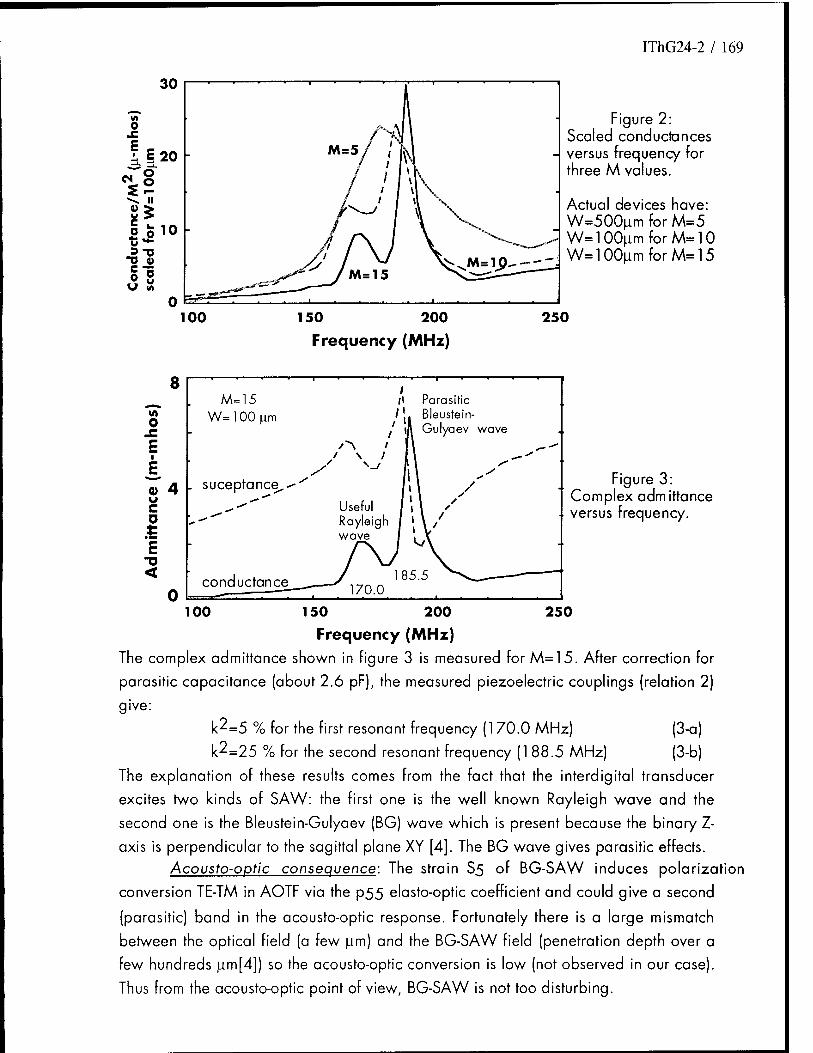
IThG24-2 / 169
Figure 2: Scaled conductances versus frequency for three M values.
Actual devices have: W=500|im for M=5 W=100ujnforM=10 W=100^mforM=15
Frequency (MHz)
8 M=15
W= 100 u.m /I Parasitic /!. Bleustein- I m Gulyaev wave
Figure 3: Complex admittance versus frequency.
100 150 200
Frequency (MHz)
250
The complex admittance shown in figure 3 is measured for M=15. After correction for
parasitic capacitance (about 2.6 pF), the measured piezoelectric couplings (relation 2)
give:
l<2=5 % for the first resonant frequency (1 70.0 MHz) (3-a)
k^=25 % for the second resonant frequency (1 88.5 MHz) (3-b)
The explanation of these results comes from the fact that the interdigital transducer
excites two kinds of SAW: the first one is the well known Rayleigh wave and the
second one is the Bleustein-Gulyaev (BG) wave which is present because the binary Z-
axis is perpendicular to the sagittal plane XY [4]. The BG wave gives parasitic effects.
Acousto-optic consequence: The strain S5 of BG-SAW induces polarization
conversion TE-TM in AOTF via the p55 elasto-optic coefficient and could give a second
(parasitic) band in the acousto-optic response. Fortunately there is a large mismatch
between the optical field (a few |im) and the BG-SAW field (penetration depth over a
few hundreds |im[4]) so the acousto-optic conversion is low (not observed in our case).
Thus from the acousto-optic point of view, BG-SAW is not too disturbing.
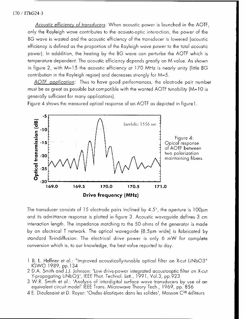
170 / IThG24-3
Acoustic efficiency of transducers: When acoustic power is launched in the AOTF,
only the Rayleigh wave contributes to the acousto-optic interaction, the power of the
BG wave is wasted and the acoustic efficiency of the transducer is lowered (acoustic
efficiency is defined as the proportion of the Rayleigh wave power to the total acoustic
power). In adddition, the heating by the BG wave can perturbe the AOTF which is
temperature dependent. The acoustic efficiency depends greatly on M value. As shown
in figure 2, with M=15 the acoustic efficiency at 170 MHz is nearly unity (little BG
contribution in the Rayleigh region) and decreases strongly for M=5.
AOTF application: Thus to have good performances, the electrode pair number
must be as great as possible but compatible with the wanted AOTF tunability (M=l 0 is
generally sufficient for many applications).
Figure 4 shows the measured optical response of an AOTF as depicted in figurel.
169.0 169.5 170.0 170.5
Drive frequency (MHz)
Figure 4: . Opical response j of AOTF between
two polarization maintaining fibers.
171.0
The transducer consists of 15 electrode pairs inclined by 4.5°, the aperture is 1 00|im
and its admittance response is plotted in figure 3. Acoustic waveguide defines 3 cm
interaction length. The impedance matching to the 50 ohms of the generator is made
by an electrical T network. The optical waveguide (8.5|im wide) is fabricated by
standard Ti-indiffusion. The electrical drive power is only 6 mW for complete
conversion which is, to our knowledge, the best value reported to day.
1 B. L. Heffner et al.: "Improved acoustically-tunable optical filter on X-cut LiNb03" IGWO 1989, pp.134
2 D.A. Smith and JJ. Johnson: 'Low drive-power integrated acoustooptic filter on X-cut Y-propagating LiNb03', IEEE Phot. Technol. Lett., 1991, Vol.3, pp.923
3 W.R. Smith et al.: 'Analysis of interdigital surface wave transducers by use of an equivalent circuit model1 IEEE Trans. Microwave Theory Tech., 1969, pp. 856
4 E. Dieulesaint et D. Royer: 'Ondes elastiques dans les solides', Masson Cie editeurs
IThG25-l / 171
Proton Exchanged LiNbÜ3 Ridge Waveguide Fabricated by Wet Etching Process
Hyung-Jae Lee and Sang-Yung Shin
Dept. of Electrical Engineering, Korea Advanced Institute of Science and Technology,
373-1, Kusong-dong, Yusong-gu, Taejon, 305-701, Korea.
(Fax) +82-42-869-3410
In general, the optical waveguide in LiNb03 integrated optics is a diffused type. Titanium
indiffusion (TI) and proton exchange (PE) are well-known fabrication methods of a diffused waveguide. On
the contrary, a ridge waveguide was fabricated by etching a LiNb03 substrate[l,2]. Etching of the LiNb03
substrate for the ridge structure was performed by a dry etching process, i.e., reactive ion etching (RIE),
reactive ion-beam etching (RIBE), etc. A wet etching of LiNb03 by using solution etchants, i.e.,
concentrated and dilute HF, HF:HN03, etc., was nearly impossible to fabricate an integrated optic device,
because of its low etch rate (several ran per minute) at room temperature and nonuniform etching[3].
Recently, it was reported that a proton-exchanged LiNb03 has an etch rate about 1000 times larger than that
of bulk LiNb03. It also has a uniform etched surface in the 1HF:2HN03 solution[4,5]. The method, wet
etching after PE, is simple and has a larger etch rate than RIE or RIBE method which has an etch rate of the
order of a few tens of run per minute. In this paper, we report a novel fabrication method of a proton
exchanged ridge waveguide by the wet etching of proton-exchanged LiNb03.
The fabrication procedure of the ridge waveguide, shown in Fig. 1, is as follows. At first, Cr strip
pattern on a LiNb03 substrate is formed by a standard photolithographic process on the Cr-sputtered
LiNb03 substrate and etching of Cr. Then, PE is performed for wet etching. This situation is shown in Fig.
1(a). Etching depth is controlled by the amount of PE, because the PE depth corresponds to the etching
depth[5]. Fig. 1(b) shows the situation after the proton-exchanged region is etched. For wet etching the
sample is immersed in a 1HF:2HN03 solution at room temperature. The Cr pattern is not attacked by the
etchant during the etching process. After the etching of the proton-exchanged region, photoresist (PR) is
coated and ultraviolet light is illuminated from the back of LiNb03 substrate. Because LiNb03 is
transparent and the Cr pattern is used as a self-aligned mask for the back-illumination process, the PR on the
Cr patten is not exposed[6]. Fig. 1(c) shows the situation. After the development of PR, Si02 is sputtered as
shown in Fig. 1(d). Then, the PR is lifted-off and the Cr patten is removed. As the next process, PE is
performed to increase the refractive index of the ridge structure by using the Si02 layer as a PE mask which
prevents the etched region from PE (Fig. 1(e)). Fig. 1(f) shows annealing process to improve the quality of
PE waveguide which has the drawbacks such as temporal instability of refractive index, degradation of
electro-optic effect, etc. If a metal layer except Cr is sputtered subsequently as in Fig. 1(d), it can be used
not only as a PE mask but also as a self-aligned electrode in X-cut or Y-cut LiNb03. In this case, the role of
Si02 is a buffer layer of the electrode.
To fabricate LiNb03 ridge waveguides, we used X-cut LiNb03 substrates. A mask with the strip
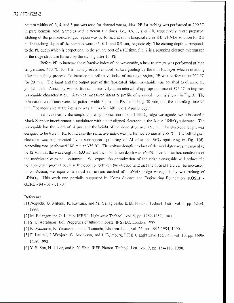
172 / IThG25-2
pattern widths of 3, 4, and 5 pm was used for channel waveguides. PE for etching was performed at 200 °C
in pure benzoic acid. Samples with different PE times, i.e., 0.5, 1, and 2 h, respectively, were prepared.
Etching of the proton-exchanged region was performed at room temperature in 1HF:2HN03 solution for 2.5
h. The etching depth of the samples were 0.5, 0.7, and 0.9 pm, respectively. The etching depth corresponds
to the PE depth which is propotional to the square root of a PE time. Fig. 2 is a scanning electron micrograph
of the ridge structure formed by the etching after 1 h PE.
Before PE to increase the refractive index of the waveguide, a heat treatment was performed at high
temperature, 450 °C, for 1 h. This process removed suface guiding by the thin PE layer which remaining
after the etching process. To increase the refractive index of the ridge region, PE was performed at 200 °C
for 20 min. The input and the output part of the fabricated ridge waveguide was polished to observe the
guided mode. Annealing was performed succesivcly at an interval of appropriate time at 375 °C to improve
waveguide characteristics. A typical measured intensity profile of a guided mode is shown in Fig. 3. The
fabrication conditions were the pattern width 3 urn, the PE for etching 30 min, and the annealing time 90
min. The mode size at 1/e intensity was 2.3 urn in width and 1.9 (im in depth.
To demonstrate the simple and easy application of the LiNb03 ridge waveguide, we fabricated a
Mach-Zehndcr interferometric modulator with a self-aligned electrode in the X-cut LiMb03 substrate. The
waveguide has the width of 4 urn, and the height of the ridge structure 0.5 urn. The electrode length was
designed to be 6 mm. PE to increase the refractive index was performed 20 min at 200 °C. The self-aligned
electrode was implemented by a subsequent sputtering of Al after the Si02 sputtering in Fig. l{d).
Annealing was performed 180 min at 375 °C. The voltage-length product of the modulator was measured to
be 12 Vmm at the wavelength of 633 nm and the modulation depth was 96.4%. The fabrication conditions of
the modulator were not optimized. We expect the optimization of the ridge waveguide will reduce the
voltage-length product because the overlap between the electric field and the optical field can be increased.
In conclusion, we reported a novel fabrication method of LiNb03 ridge waveguide by wet etching of
LiNb03. This work was partially supported by Korea Science and Engineering Foundation (KOSEF -
OERC-94-01 -01 -3).
Reference
[1] Noguchi, O. Mitomi, K. Kawano, and M. Yanagibashi, IEEE Photon. Technol. Lett., vol. 5, pp. 52-54,
1993.
[2] M. Belanger and G. L. Yip, IEEE J. Lightwave Technol., vol. 5, pp. 1252-1257, 1987.
[3] S. C. Abrahams, Ed., Properties of lithium niobate, INSPEC, London, 1989.
[4] K. Mizuuchi, K. Ymamoto, and T. Taniuchi, Electron. Lett., vol. 26, pp. 1992-1994, 1990.
[5] F. Laurell, J. Webjorn, G. Arvidsson, and I. Holmberg, IEEE J. Lightwave Technol., vol. 10, pp. 1606-
1609, 1992.
[6] Y. S. Son, H. J. Lee, and S. Y. Shin, IEEE Photon. Technol. Lett., vol. 2, pp. 184-186, 1990.

IThG25-3 / 173
/VE
(a)
/ Cr
(b)
/ PR
(c)
t t t UV
SiO,
/
(d)
PE Si02
(e)
(f)
Fig. 1. Fabrication procedure of ridge waveguide:
(a) waveguide patterning and PE (b)
etching of proton-exchanged LiNb03 (c)
back-illumination (d) development and
Si02 sputtering (e) lift-off and PE (f)
annealing
Fig. 2. Scanning electron micrograph of ridge
structure
0.9 71 1
0.9
0.8 '
0.8 - „0.7
CD
>-0.6
CO
2 0.5 (- z
■
0.7
0.6
0.5
■
g0.4 - 0.4
0.3
- 5
0.3
■
-
0.2 ■
0.2 - 0.1 0.1 -
0 5 WIDTH [U
1C
Ml 0 5
DEPTH [UM) 10
Fig. 3. Typical measured intensity profile of
ridge waveguide

174 / NOTES

8:30 am-10:00 am Salon 1
Friday, February 24, 1 995
Plenary Session: 2
Steve Korotky, Presider AT&T Bell Laboratories

176 / L3-1
Integrated Photonics in the RACE Program
Paul Lagasse University of Ghent
41 St. Pietersnieuwstr., Ghent, Belgium B-9000
The most significant research results obtained in the European RACE II program in the field of integrated photonic circuits and their system applications will be reviewed.

L4-1/ 177
New Technical Career Strategy
Milton Chang New Focus, Inc.
1275 Ream wood Avenue Sunnyvale, CA 94089
Tremendous opportunities await people with a technical education who are willing to take a broader view of their skills. A low-risk model to start a business will also be presented.

178 / NOTES

ay, February 24, 1995
Semiconductor Lasers and Amplifiers
IFA 10:30 am-12:00 m Salon 1
Robert J. Deri, Presider Lawrence Livermore National Laboratory
180 / IFAl-1
Long Wavelength Vertical Cavity Surface Emitting Lasers
John E. Bowers University of California-Santa Barbara
Santa Barbara, CA 93106
Summary not available.

IFA2-1 / 181
High-temperature cw operation of a double-heterostructure laser emitting at 1.3 urn on Si substrate
Takeshi Yamada, Masami Tachikawa, Tohru Sasaki, Hidefumi Mori, Yoshiaki Kadota, and Mitsuo Yamamoto
NTT Opto-electronics Laboratories, 3-1 Morinosato Wakamiya, Atsugi-shi, Kanagawa 243-01, Japan Tel. +81 462 40 3254 Fax. +81 462 40 4304
INTRODUCTION Optical devices on Si substrate will be used for opto-
electronic integrated circuits (OEICs) such as the interconnec- tions for computer systems and subscriber systems. Long-wave- length InP-based devices on Si are promising for OEICs,1' though InP on Si has a high lattice mismatch of 8%. Photodiodes on Si have been shown to perform comparably to those on InP. ' Cw stable operation has been demonstrated with a 1.5-um laser on Si at room temperature ' , but for 1.3-um lasers on Si, it has not been obtained. Though there are some reports on LDs on Si, the quality of those LDs is not yet comparable to ones on InP. And cw operation at higher temperature such as the 50 °C, employed in life tests, has not been reported, as far as we know.
This is the first report of a 1.3-um laser on Si that oper- ates at cw at temperatures higher than 50 °C. The quality of the lasers on Si was compared and indicated as high as that on InP, at the first time.
EXPERIMENTAL The InP on Si substrate was grown hetero-epitaxially as
shown in Fig. 1. A 2-um-thick n-type GaAs layer and five pairs of strained layer superlattice consisting of InP and InGaAsP were grown on Si substrate by low pressure metalorganic chemical vapor deposition (MOCVD). Then, 13-nm-thick n-type InP was grown by vapor mixing epitaxy (VME) with thermal annealing. The InP layer has the highest quality ever reported: the etch pit density (EPD) and full width half maximum (FWHM) of x-ray diffraction for the layer are 5x10 cm and 65", respectively.
A laser structure was grown by MOCVD. The double hetero (DH) laser structure consists of 0.1-urn-thick InGaAsP confinement layer, 0.15-um-thick InGaAsP active layer of 1.3-um composite, 0.1-um-thick InGaAsP confinement layer, 1.5-um-thick p-InP layer and 0.4-um-thick p+-lnGaAsP contact layer. The laser structure on InP was grown simultaneously to compare it to the laser on Si. Both laser structures were processed into low-mesa-type ridge waveguide lasers. The width of the ridge waveguide was 4 um (3 um for the LD on InP) and the length was 300 um. The mirror was made by cleaving and had no coating.
RESULTS AND DISCUSSION The threshold current density was estimated for broad area
electrode LDs with a 40-um width. The threshold current density was as low as 0.7 kA/cm for a 1000-um-long LD on Si. Light-
182 / IFA2-2
current characteristics of the LD on Si operated at cw are shown in Fig. 2 for various temperatures. The threshold current was 36 mA and the slope efficiency was 0.19 W/A at 20 °C. The light output was as high as 18 mW/facet at the driving current of 150 mA. At 50 °C, the LD on Si had the threshold current of 56 mA and the slope efficiency of 0.15 W/A.
The temperature dependence of the threshold current on Si is compared to that on InP in Fig. 3. The LD on Si was operated at up to 75 °C, and one on InP up to 95 °C. The characteristic temperatures TQ for the LD on Si and on InP were 65 K and 69 K, respectively. The values were very close to each other. The reason the LD on Si stopped operating at a lower temperature than the one on InP may be due to the fact that the LD on Si had a higher threshold current.
The histogram of the threshold current at 20 °C by pulse operation for LDs on Si is compared to that for the LDs on InP in Fig. 4. Though the average of the LDs on Si is approximately 5 mA larger than the average of those on InP, the distribution profiles are very similar. This similarity indicates the uni- formity of the LDs on Si. The difference in the threshold cur- rent is partly attributed to the difference of the ridge width. The distribution of the efficiency for the LDs on Si is also almost the same as those on InP. These results indicate the quality of the LD on Si is comparable to those on InP at room temperature.
A preliminary aging test was performed on a LD on Si. The cw driving current for constant light output of 1 mW/facet at 50 °C is shown in Fig. 5. The driving current at 50 °C increased 4 % during the first ten hours, then increased gradually. The life determined at a 50 % increase in driving current was approximate- ly 1100 hrs. The LD on Si operated for more than 1300 hrs at 50 °C. At 25 °C, the curve for the increase in the driving current was similar in shape to that at 50 °C. After 800 hrs operation, the driving current increased 10 %. Extrapolation to 50 % in- crease in driving current suggests a life of 40000 hrs under the condition of light output of 1 mW/facet at 25 °C.
CONCLUSION We have observed, for the first time ever, cw operation of
1.3 jum DH LDs epitaxially grown on Si above 50 °C. The LD on Si operated at up to 75 °C. The LD on Si operated at 50 °C with the light output of 1 mW/facet for as long as 1300 hrs. These results were obtainable due to the high quality of the threshold current of 36 mA and slope efficiency of 0.19 W/A. The histogram of the threshold current and the efficiency of LDs on Si were very similar to those on InP.
References 1)M. Razeghi, et al.: Appl. Phys. Lett. 51, 1271 (1987) 2)T. Sasaki, et al.: Appl. Phys. Lett. 64, 751 (1994) 3)M. Sugo, et al.: SSDM Extendid Abstracts, 656 (1992) Tsukuba

IFA2-3 / 183
InP +InGaAsP contact layer
InGaAsP DH structure
GaAs(2um)+ SLS+InP(13um)
Si substrate
Fig. 1 Schematic diagram of the DH LD on Si substrate.
20
c5 15 o
3 10 Q.
O
O) 5 "
0
I 1 0 /20C
cw //30°C ///40C
// Y / 5° c~ /^ 60 C_
/////, ^--70OC
0 50 100 150 200 Driving current (mA)
Fig. 2 Temperature dependence of I-L characteristics for the LD on Si.
4.5
3.5
i 1 1 r
on Si (
To=65K 0°
on InP To=69K
i i i i J L
290 310 330 350 370 Temperature (K)
Fig. 3 Temperature dependence of the threshold current for the LD on Si compared to that on InP at cw.
0 10 20 30 40 Threshold current (mA)
Fig.4 The histogram of the threshold current for the LDs on Si comparing
to those on InP.
< E c CD
o
>
Fig
400 600 800 1000 1200
Driving time (hr)
5 The preliminary life test for the LD on Si at 50 C.

184 / IFA3-1
ACCURATE DETERMINATION of TRANSPARENCY CURRENT in PACKAGED SEMICONDUCTOR LASERS and SEMICONDUCTOR OPTICAL AMPLIFIERS
F.G. Patterson, S.P. Dijaili and R. J. Deri, Lawrence Livermore National Laboratory, Livermore, CA 94550
The reliability of semiconductor laser diodes and related devices is a significant issue for their deployment in many applications [1,2], creating demand for device diagnostics applicable to packaged devices. Measurements of the transparency current density (Jo) in laser diodes and traveling-wave semiconductor optical amplifiers (SOAs) can provide such a diagnostic. It is essential, however, to measure Jo on packaged devices, so that they can be characterized after aging or degradation. This precludes techniques requiring data from multiple devices (e.g., an ensemble with different lengths). Jo is conventionally measured using a junction-voltage technique [3,4], in which an input optical signal induces a change in carrier density in the active region due to stimulated absorption or emission. The result is a voltage drop across the diode. At material transparency, the stimulated absorption is exactly balanced by the stimulated emission and the voltage drop goes to zero. Since the polarity of the voltage drop changes sign at current densities above Jo, the optical input beam is typically modulated and lock-in amplification is employed to sensitively detect the polarity sign flip. Here we show that this technique is not reliable for certain types of laser structures, because the deduced Jo is strongly dependent on device packaging—that is, the measured Jo varies with the manner in which light is coupled into the diode waveguide. For packaged SOAs, we propose and demonstrate an alternative all-optical technique to overcome this problem. One important advantage of the optical method over the junction voltage method is that the actual device optically-guided mode is directly sampled. In the case of packaged semiconductor lasers, our all-optical method can complement the junction-voltage method to resolve device versus packaging degradation.
The essence of our all-optical technique for determining Jo is shown in Fig. 1. A modulated (e.g., chopped at 350 Hz) pump beam (at A,pUmp) is coupled into facet 1 of a laser diode or SOA. Below the transparency current density (Jo) the pump beam will saturate the
absorption and increase the transmission for a second laser beam (at Xprobe) or for the amplified spontaneous emission (ASE) generated in the test device. At current densities greater than Jo the pump beam will saturate the material gain and thereby decrease the transmission for other optical signals in the guided-wave device. At exactly Jo, the pump beam does not modulate the other optical signal beams because neither saturable absorption or gain is present. Typically, the monitor signals are spectrally filtered in an optical spectrum analyzer (OSA, Hewlett-Packard 71451 A) and detected with a lock-in amplifier. Since the semiconductor gain media are homogeneously-broadened, this method is largely insensitive to the wavelength of the detected light (Jo for ^pump is being measured).- Several laser diodes and SOAs have been carefully characterized and a comparison of results obtained using a tunable probe beam as well as ASE at different center wavelengths and bandwidths show that the technique is sensitive and reproducible.
Laser diode pump and probe or SOA
probe signal signals in to OSA —► \ ^—ASEj^U) (2> <y optional f or ASE to
OSA
Fig. 1: Setup for measuring the transparency current of a laser diode or SOA using saturation-induced crosstalk. An optical spectrum analyzer (OSA) is utilized to spectrally filter the desired optical monitor signal: either forward or backward ASE or a weak probe beam (A,probe^pump) m the forward direction. At Jo, no pump-induced modulation of the optical monitor signal occurs because neither saturable absorption or gain is present.
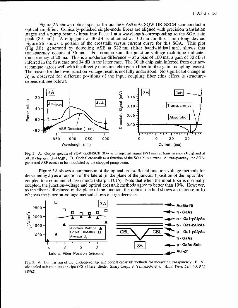
IFA3-2 / 185
Figure 2A shows optical spectra for our InGaAs/GaAs SQW GRINSCH semiconductor optical amplifier. Conically-polished single-mode fibers are aligned with precision translation stages and a pump beam is input into Facet 1 at a wavelength corresponding to the SOA gain peak (891 nm). A chip gain of 30 dB is obtained at 100 ma for this 1 mm long device. Figure 2B shows a portion of the crosstalk versus current curve for this SOA. This plot (Fig. 2B), generated by detecting ASE at 922 nm (filter bandwidth=l nm), shows that transparency occurs at 36 ma. For comparison, the junction-voltage technique indicates transparency at 28 ma. This is a moderate difference — at a bias of 100 ma, a gain of 30 dB is inferred in the first case and 34 dB in the latter case. The 30 db chip gain inferred from our new technique agrees well with the directly measured chip gain (fiber to fiber gain - coupling losses). The reason for the lower junction-voltage result is not fully understood. No significant change in JO is observed for different positions of the input coupling fiber (this effect is structure- dependent, see below).
■80- i r
850 900 950 1000
Wavelength (nm)
</}
2 0.00 ü
20
Current (ma)
Fig. 2: A. Output spectra of SQW GRINSCH SOA with injected signal (891 nm) at transparency (J=Jrj) and at 30 dB chip gain (J=J30dB)- B- Optical crosstalk as a function of the SOA bias current. At transparency, the SOA- generated ASE ceases to be modulated by the chopped pump beam.
Figure 3 A shows a comparison of the optical crosstalk and junction-voltage methods for determining Jo as a function of the lateral (in the plane of the junction) position of the input fiber coupled to a commercial laser diode (Sharp LT015). Note that when the input fiber is optimally coupled, the junction-voltage and optical crosstalk methods agree to better than 10%. However, as the fiber is displaced in the plane of the junction, the optical method shows an increase in Jo whereas the junction-voltage method shows a large decrease.
2500-
E 2000- o
~ 1500H
1000- A
3A D
□ D □ a "A * * A
Junction Voltage A Optical Crosstalk □ Average J0
CBL \A CBL
T T 1 r
4-202
Lateral Fiber Position (microns)
3B
Au-Ge-Ni
n - GaAs
n- Ga1-yAlyAs
p- Ga1-xAlxAs
p- Ga1-yAlyAs
n - GaAs
p - GaAs Sub.
Au-Zn
Fig. 3: A. Comparison of the junction-voltage and optical crosstalk methods for measuring transparency. B. V- channeled substrate inner stripe (VSIS) laser diode. Sharp Corp., S. Yamamoto et al., Appl. Phys. Lett. 40, 972 (1982).

186 / IFA3-3
One plausible argument for the transparency current dependence on horizontal displacement of the injected light is as follows. We refer to Fig. 3B showing the current blocking layers (CBL) of the Sharp laser diode. For the case of the optical method of determining Jo, the current density decreases laterally along the active region. These regions are pumped less so the overall current needs to be increased in order to reach transparency. The transparency current therefore increases with lateral displacement of the injected light. For the case of the junction-voltage method, the CBL region absorbs the injected light as it is horizontally displaced. The reverse bias junctions of the CBL act as photodiodes and thus a net excess of holes on the p-side of the active region tends to increase the forward current, thereby reducing the current needed from the external supply. This explanation requires further study. A very similar lateral Jo dependence has also been observed in another commercial laser diode which has a different device structure (Hitachi HLP1400, channel substrate planar).
The solid curve in Fig. 3A plots the average of the two transparency methods. This averaged parameter is relatively insensitive to the input fiber coupling and closely represents the true transparency current density. By making both measurements and tracking the changes over time, once can determine whether performance degradations originate in the device or the fiber- coupled package.- The optical technique for measuring transparency described here works well for both semicondductor lasers and optical amplfiers because access to only one optical facet is required. Additional information concerning the longitudinal distribution of gain anomalies (defects) may be obtained by comparing the measured Jo from opposite ends of a device with both facets accessible (details will be presented at the conference).
In conclusion, we have demonstrated a new all-optical technique for measuring the transparency current of semiconductor lasers and optical amplifiers. For SOAs, the technique is deemed superior to the junction voltage method because the measurement is performed on the actual optically guided-mode of interest. This has particular relevance to packaged devices since we have shown that in some structures the measured Jo is dependent upon the alignment of the fiber pigtail. Finally, monitoring Jo over time using both the optical and voltage methods can provide a simple method for tracking the aging of packaged SOA and laser devices.
We thank Holly Petersen and Richard Combs for technical assistance. This work was performed under the auspices of the U.S. Department of Energy under contract W-7405-ENG- 48.
References: 1. L.F. DeChiaro, M. Robin, et al., J. Lightwave Technol. 11, 2057 (1993). 2. M.C. Wang, D.M. Hwang, et al., Appl. Phys. Lett. 64, 3145 (1994). 3. V.V. Luc, P.G. Eliseev, et al, J. Quantum Electron. 19, 1080 (1983). 4. A. Alping, B. Bentland, et al., Electron. Lett. 20, 794 (1984). 5. B. Saint-Cricq, S. Bonnefont, et al., Electron. Lett. 27, 865 (1991). 6. T.R. Chen, L.E. Eng, et al., Appl. Phys. Lett. 56, 1002 (1990).

IFA4-1 / 187
Analysis of Multi-Wavelength DFB Laser Arrays with Different Ridge Widths
A.M. Sarangan, C.L. Xu, W.P. Huang
Department of Electrical and Computer Engineering University of Waterloo, Waterloo, Ontario, N2L 3G1, Canada
Tel: (519) 885-1211, Fax: (519) 746-3077
G.P. Li, C. Wu, T. Makino
Advanced Technology Laboratory Bell-Northern Research, Ottawa, Ontario, K1Y 4H7, Canada
Tel: (613) 763-9644, Fax: (613) 763-4147
For WDM optical sources, fixed wavelength laser arrays are a cheaper and practical alternative to widely tunable lasers. Further, if the wavelength of each source in the array can be denned by lithography instead of selective growth this alternative becomes even more attractive. Several techniques are available for this, including ridge width variation [1], ridge angle variation [2] and thermal tuning [3]. In this paper we report simulation and experimental study of the CW char- acteristics of varying ridge width laser arrays. In particular this type of structure allows one to separate out the material aspects of the laser from the geometry dependent aspects, giving more insight into those over which the designer has control.
In this work we perform a fully two-dimensional finite difference analysis of the optical mode taking the detailed MQW structure into account [4]. This optical mode is then used for calculating threshold current and wavelength shift. In particular, the carrier profile under the ridge is modelled using the characteristic diffusion length L [5]. Using £ as a material parameter that can be varied, we find that the gain profile g(x) can be significantly different for different L (figure 2). As the ridge width is increased the field overlap with the gain profile increases, however due to the larger ridge the threshold current increases. At smaller ridge widths the optical profile is less confined resulting in a smaller overlap between the gain and the field, again resulting in a larger threshold current again. Therefore, we find a minimum in the threshold current vs ridge width curve. In
general the threshold current increases with increasing L.
The modal gain and the coupling coefficient are calculated from the 2-D optical field as:
am (G, L, W) = W71 JJ\E(x,y)\ dxdy
and 2 ,„.. k JJ\E2(x,y)\ n(x,y)An(x,y)dxdy V ' 2neff JJ\E>(z,y)\2dzdy
Nqw is the number of quantum wells, An is the index corrugation along the cavity and E (x,y) is
the lateral electric field distribution.
The gain g (x) is a function of the volume injection rate G in the quantum wells. The threshold

188 / IFA4-2
value of G is obtained by solving
0Lm{G,L,W)-ao[K(W)} = Q
where a0 is the DFB threshold gain due to the corrugation n. The total threshold current is therefore:
Ith = 2qWltG
where I is the length of the cavity and t is the total thickness of the quantum wells.
Figure 3 shows the threshold current dependence on ridge width for different diffusion lengths. On the same figure the experimentally measured data is also shown. The diffusion length can, in some sense, be treated as a fitting parameter. From the figure, its value can be extracted to be somewhere between l//m and 2/zm.
The lasing wavelength at threshold is:
x_2neff(W)A
1 + A6r(W)
where A is the grating pitch and <!>T is the real part of the detuning factor at threshold. For the loss coupled structure, figure 3 shows the simulated and measured curve for wavelength dependence on ridge width.
In this presentation we will be showing details on the laser array as well as the modelling details.
References
[1] G.P. Li et al. Multi-wavelength ridge waveguide quantum well gain-coupled dfb laser array. OSA Annual Meeting, 1994.
[2] W.T. Tsang et al. Control of lasing wavelength in distributed feedback lasers by angling the active stripe with respect to grating. IEEE Photonics Technology Letters, 5(9):978-980, 1993.
[3] Y.H. Lo et al. Four channel integrated DFB laser array with tunable wavelength spacing and 40Gb/s signal transmission capacity. /. Lightwave Technology, ll(4):619-623, 1993.
[4] M.S. Stern. Semivectorial polarised finite difference method for optical waveguides with arbi- trary index profiles. IEE Proc, 135(l):56-63, 1988.
[5] B.W. Hakki. Carrier and gain spatial profiles in GaAs stripe geometry lasers. J. of Applied Physics, 44(ll):5021-5028, 1973.

IFA4-3 / 189
1.2
1
0.8
0.6
0.4
0.2
Current
-*= = 1! 11 H = =»-
y = d
x=-W x=0 x=W
Figure 1: Current injection and lateral diffusion under the ridge
Gain (L=5.0um) Gain(L=1.0um)
0 -10 -8 -6 -4
0.6
0.5
0.4
0.3
0.2
0.1
0
0.7um Ridge
Gain (L=5.0um)
Optical Intensity
Gain (L=1.0um)
Gain (L=2.0um)
-2024
x Distance (um)
6 8 10 -3 -10 1
x distance (urn)
Figure 2: Optical field profiles and gain profiles g (x) for two ridge widths
Threshold Current (mA)
100
90
80
70
60
50
40
30
20
10 10 12
Ridge Width (um)
3 4 5 6 7
Ridge Width (urn)
8 9 10
Figure 3: Threshold Current and Wavelength vs Ridge Width
190 / IFA5-1
1.3 Jim Wavelength, InGaAsP/InP Etched-Facet Folded-Cavity
Surface-Emitting Lasers for Photonic Integration
C-P Chao, G-J Shiau*, D. Garbuzov and S. R. Forrest
Advanced Technology Center for Photonics and Optoelectronic Materials
Department of Electrical Engineering
Princeton University
Princeton, NJ 08544
(609) 258-4204
FAX (609) 258-1954
*Department of Materials Science, University of Southern California
Los Angeles, CA 90089-0241
Long wavelength surface-emitting lasers with output light perpendicular to the wafer
surface are attractive for photonic integration [1-5]. Among different surface-emitting laser
structures, folded-cavity surface-emitting lasers (FCSEL) are suitable for monolithic
integration with other optoelectronic devices for applications in two-dimensional optoelectronic
interconnections and smart pixels [6].
In this work we report the fabrication of 1.3 |im wavelength, strained MQW
InP/InGaAsP FCSELs with a 45° angle facet and a vertical facet. With both facets dry-etched,
these devices can be tested at wafer level and easily integrated with other long wavelength
optoelectronic devices. A low threshold current of 32 mA and 18% efficiency for the surface-
emitted light was achieved for 4 |im wide by 600 (im long devices. To our knowledge, this is
the first demonstration of an integrable InP/InGaAsP FCSELs, and the threshold current is also
the lowest reported for 1.3 |J.m wavelength FCSELs.
The laser material was grown by gas-source molecular beam epitaxy on a n+ (100) InP
substrate. A ljim thick Si-doped InP lower cladding layer was first grown, followed by a
1000Ä thick, undoped InGaAsP lower waveguide layer (bandgap cutoff wavelength X,g=1.15(im). After growth of the undoped active region, a 1000Ä thick InGaAsP
(^g=1.15p.m) upper waveguide layer was grown. The undoped active region consists of five
compressively strained InGaAsP quantum wells with 100Ä wide barriers (kg=1.15\lm) and
60Ä wide wells (^g~1.4|im). Finally we grew a l|im thick Be-doped InP upper cladding layer
and a 800Ä thick Be-doped p+ InGaAs top contact layer
The device, shown schematically in Fig. 1, exploits a 45° facet, a vertical facet, and a 4
|im wide ridge waveguide, all dry-etched by a CEUXEL: plasma. The device processing started
IFA5-2 / 191
from patterning 1000Ä thick PECVD SiNx as a ridge waveguide dry etching mask. The ridge
etching stopped ~ 2000Ä above the undoped waveguide region. Next, a 5000Ä thick SiNx
layer was deposited, and the SiNx on top of the ridge was removed by a photoresist
planarization process. A Ti/Pt/Au (200Ä/500Ä/4000Ä) p-contact pad was then deposited,
followed by a 3000Ä thick SiNx mask for etching both the vertical and the 45° facet. All three
dry-etching procedures were carried out in a conventional reactive ion etching system using a
5:1 CH4:H2 mixture at 30 mTorr with a 650V self-bias. A custom designed wafer holder
following a design previously reported[7], was used for the 45° facet formation. The etch rate
was ~550Ä/min for the normal facet and ~250Ä/min for the angled facet. Smooth and highly
directional etching of both the vertical and 45° facets was observed by scanning electron
microscopy. After facet etching, we deposited Ge/Au/Ni/Au (270Ä/450Ä/215Ä/1200Ä) for n-
contact metal to the substrate.
The devices were tested at wafer level, and Fig. 2 shows the room temperature light-
current characteristics for a 4 Jim wide by 600 Jim long folded-cavity laser. The threshold
current is 32 mA, with an external quantum efficiency of 18% for surface-emitted light. More
than 7 mW surface-normal output light power was measured. The threshold current is the
lowest reported for 1.3 |im wavelength FCSELs, and the efficiency is comparable with
FCSELs with one cleaved, vertical facet[8]. The peak emission wavelength is around 1.32 [im
as shown in the inset of Fig. 2, and a 15 dB mode suppression was observed up to 45 mA.
In conclusion, we have fabricated an etched-facet 1.3 (im wavelength FCSEL with a
threshold current of 32 mA. To our knowledge, this is the first demonstration of high
performance etched-facet 1.3 )J,m FCSELs. These etched-facet devices with surface-normal
light output are useful for optoelectronic integration.
The authors thank Rome Labs (Hanscom)/ARPA, US Army Research Labs, and
AFOSR for their support of this work.
IJ s**. 4- f**. -ff** y^ /** /"fc o •
1. H. Wada, D. I. Babic, D. I. Crawford, J. J. Dudley, J. E. Bowers, E. L. Hu, and J. L. Merz, B. I. Miller, U. Koren, and M. G. Young, IEEE Photon. Tech. Lett., p. 977, 1991. 2. T. Baba, K. Suzuki, Y. Yogo, K. Iga, and F. Koyama, IEEE Photon. Tech. Lett., p. 744, 1993. 3. Z. L. Liau and J. N.Walpole, Appl. Phys. Lett., vol. 46, p. 115, 1985. 4. H. P. Lee, A. Scherer, E. D. Beebe, W. P. Hong, R. Bhat and A. A. Koza, Electron. Lett., 1991. 5.B. Stegmüller, H. Westermerier, W. Thulke, G. Franz, and D. Sacher, IEEE Photon. Tech. Lett., vol. 3, p. 776, 1991. 6. S. Yu and S. R. Forrest, J. Lightwave Tech., vol. 11, No. 10, P. 1659, 19936. 7. T. Takamori, L. A. Coldren, and J. L. Merz, Appl. Phys. Lett., vol. 53, p. 2549, 1988. 8. C-P Chao, G-J Shiau, and S. R. Forrest, IEEE Photon. Tech. Lett., (Dec, 1994).

192 / IFA5-3
Dry-etched ridge
Surface-emitted light
A
Etched vertical facet
Strained MQW
45" angled facet
Fig. 1. Schematic diagram of a 1.3 |im wavelength GalnAsP/lnP FCSEL with dry-etched 45° facet and vertical facets.
8
7
6
5
4
3
2
1
0
1 r
_ RT, 600|am X 4jim
J 1.3096 1.3196 1.3296
Wavelength ((im)
20 40 60
Current (mA)
80 100
Fig. 2. Light-current characteristics and emission spectrum of a 600 um x 4 jim etched-facet FCSEL.
, February 24, 1995
Waveguide Modeling Techniques
IFB 10:30 am-12:00 m Salon 4
John Michael Zavada, Presider U.S. Army Research Office
194 / IFBl-1
Semi-Vectorial Response of Three-Dimensional Reflecting Structures via
Iterative Solution of the Helmholtz Equation
G. Ronald Hadley
Sandia National laboratories
Albuquerque, New Mexico 87185-5800
(505)844-4015
Waveguiding structures that generate reflections are currently modeled
by a number of different methods, most of which are of very limited generality.
Of these methods, only the finite-difference time-domain (FDTD) method1 has been
shown to be useful over a wide class of structures. Unfortunately, this technique
is very costly in terms of computer resources, thus limiting its utility. In
order to address this need, we recently reported a new modeling technique2 that
involves the iterative solution of the scalar Helmholtz Equation using the ADI
(alternating direction implicit) method. That technique was limited by two major
restrictions: (1) Proper convergence of the iteration required an appropriate
absorbing layer around the problem region periphery, and (2) The method as stated
was only valid for 2D problems, although it was pointed out that an extension
to three dimensions seemed feasible. In this paper we remove both restrictions
and model three-dimensional structures by iterative solution of the scalar Helm-
holtz Equation with normalized coordinates,
V2A + e(x,y, z)A = 0 (l)
where we keep only a single field component, but employ correct boundary con-
ditions on interfaces separating regions of uniform dielectric constant, thus
providing a semi-vectorial method that is accurate for TE- or TM-like modes. In
case a field component is discontinous at an interface, we store the average
field value, and account for the discontinuity in the difference equations.
Our solution method employs a generalization due to Douglas3 of the
well-known ADI algorithm,
1 n + ■
(co„ + 52)/l 3 = (o)n- 52 -25J-252) A" 2 1
n + - " + - _ (2) (co„ + 52)A 3 = anA 3 + 52,4"
2
(con + 52)A" + 1 = unAn + i + 8^An

IFB1-2 / 195
where the operators 8^, 8^, 8^ are defined by
(3)
s24| -Ai + l,j.k + Ai-l,j,k 2Ai,j,k £i,j,kA
x%.r (Ax)* 3 A^k
9L2A\ AiJ+l,k + Ai,i-l,k^'2'Ai,j,k , Ei,j,kA 8^L*" —w?— "3"^-* s24| _ Ai,y, fc+ 1 + Ai,j,k- 1 ~ 2Ai,j, k Ei,j, kA ö~ L-j.r (up —Au* z
The field amplitude A is chosen to be the X -component of E for TE polarization,
and the parameters CO are chosen to optimize convergence. We utilize a two-
parameter sequence whose values are similar (but not identical) to values used
for solving two-dimensional problems. Differences arise due to the different
convergence rates for various spatial frequencies for the two schemes.
In agreement with theoretical expectations, it has been determined that
the use of absorbers around the problem region periphery is unnecessary, pro-
vided that some form of transparent boundary condition is utilized. In practice,
a simple non-adaptive boundary condition of the form A„ = Aw_, exp (ikAx)
appears to work quite well. More study is required to identify a successful
adaptive form.
As an illustration of the ability of this technique to model realistic
structures, consider the problem shown in Fig. 1, containing a waveguide into
which has been etched a first-order Bragg grating. Such structures are important
as components of waveguide Fabry-Perot cavities, but cannot be reliably modeled
in two dimensions due to the quasi-circular mode shape. The response of a 40
period section of this structure to the waveguide fundamental TE eigenmode (as
modified by the grating) was computed using the technique described previously.
The converged solution (obtained in about 2 hours on a fast workstation) is shown
in section in Fig. 2. The grating coupling coefficient is inferred from a cal-
culation of the reflection coefficient of this short section, thus allowing a
prediction of the entire device. We believe that this is the first such simu-
lation to be reported. Future calculations of this type will allow a study of
the tradeoff between lateral confinement and grating efficiency as the etch
depth is varied.
1. W. P. Huang, S. T. Chu, A. Goss, and S. K. Chaudhuri, IEEE Phot. Tech. Lett.
Vol. 3, No. 6, 524 (1991) .
2.G. R. Hadley, Optics Letters, Vol. 19, No. 2, 84(1994).
3.J. Douglas, Numericshe Math. Vol. 4, 41(1962).

196 / IFB1-3
Fig. 1. Problem geometry for the simulation of a first-order Bragg grating etched
into a rib waveguide. Only the left half of the symmetric structure is shown.
Fig. 2. Intensity contours in the cutaway section for the converged solution.
Propagation is towards positive z, with y-z a symmetry plane.
IFB2-1 / 197
Simulation of Guided Wave Structures of Arbitrary Geometry Using Boundary Integral Method
Wei Yang and Anand Gopinath
Department of Electrical Engineering University of Minnesota, Minneapolis, MN 55455
Guided wave structures with increasing complexity have been a persistent challenge to integrated
photonic device modeling. Direct approaches to solving wave equations, either in the finite
difference or the finite element scheme, lead to excessive consumption of computational resources.
This is because large number of nodes over the domains of interest are needed in order to
accurately represent the differential equations. The number of nodes can be enormous even in
some moderately complex structures, therefore device modeling based on wave analysis can be
extremely costly. Although many special techniques have been developed for specific structures,
generic and accurate simulations are often difficult. Beam propagation method (BPM) [1] is very
efficient in studying paraxial propagation problems but is not suitable for structures with reflections
or large angle bends. The boundary integral method we introduce in this paper, instead of solving
the wave equations in the whole domain, only solves boundary values through integration. In
most applications it significantly reduces computation time and storage because nodes on the
boundaries are much less than nodes needed for the whole domain. Other advantages of the
method include the flexibility of treating arbitrary boundaries, easy implementation of boundary
conditions, and the simplicity of mesh setup.
Consider piecewise homogeneous domains (n=l,2,3...) with propagation constants ßn which are
separated by a series of boundaries. Given any point ro in domain n, by Green's theorem, the
scalar field can be expressed in terms of the boundary values:
where the integral is performed on the boundary and Gn is the Green function in the domain, which is exp(jßnr))/(47tr) for 3-D and Ho(ßnr)/(4j) for 2-D. Therefore the complete solution is
obtained if all the boundary values are known. Now we set N points on the boundaries, and for
simplicity these points are uniformly spaced and each point occupies a unit area (or unit length for
2-D domain). The scalar field and its normal gradient at point / are denoted by % and \j/i=d(pi/dn.
Note that since these values are shared by both sides of the boundary, continuous boundary
conditions are applied. We also define operator 5// =1 for boundary point i andy on the same

198 / IFB2-2
domain, and <5y -0 otherwise. Apply Green's theorem, and replace the integral in (1) with
summation, for boundary point /, the scalar field (pi can be evaluated from either left or right side
of the boundary, and it can be proved that
for; on the left, fa = £ q>j—^^ $ij -EGi(rfri) Wj^ij + Sü (2)
for; on the right, fa = _£ y. —cL&£Z §.. +J^G^r,-/-;) y/,- 5,y + Sri (3)
where G/ and Gr are Green functions in the left and right side domains, Si and Sr are left and right
side integral contributions from the sources, which are boundaries with known field values. The
sign change in (3) is due to the definition of normal direction. Linear system (2), (3) of 2N
equations and 2N unknowns (% y/[) can be explicitly solved. Note that evaluation of the matrix
elements is merely a task of calculating Green functions for pairs of points, and since many points
may not "see" each other (Sy =0), the matrix is sparse in most structures.
Based on the method described above, we have developed a 2-D scalar simulator which has
demonstrated powerful capability of handling several guided wave structures that are difficult for
BPM. In these structures the optical fields are confined in one dimension and propagate in the
other two dimensions. Without resorting to 3-D modeling, we used effective indices to represent
different propagation constants in different regions. This helps us concentrating on the radiation
modes in the two propagation dimensions, assuming that the confined dimension only affects the
propagation constants. Regions where waves do in fact radiate in all dimensions, such as air, were
treated approximately by assuming an effective index of 1. This has little effect on the guided
region as long as free space couplings are not involved. To model radiation modes in all
dimensions, we have to extend the current 2-D modeling to 3-D. However, this extension is quite
straight forward. 2-D simulations have been performed on some waveguiding structures designed
for GaAs/AlGaAs system. Fig. 1 shows the results for a right angle bending structure with a 45°
corner reflector. The reflector is fabricated by etching through the guiding layer and forming a
vertical facet. The input Gaussian beam is guided to the mirror region and mostly reflected into
the output arm, with obvious beam profile distortion due to higher order modes generation.
Similar results are observed in a symmetric power splitter with two 45° corner reflectors and a
tapered inlet, as shown in Fig. 2. Radiation losses of these structures can be readily obtained from
the simulations, which are currently under investigation.
References
(1) M. D. Feit, J. A. Fleck, Appl. Opt. 17, p3990, 1978

IFB2-3 / 199
Input
Output
Fig. 1. Beam propagation in a waveguide 90° bending structure, where a 45° angled mirror is placed at the corner
Fig. 2. Beam splitting symmetrically into two guides. Two 45° angled mirrors are used at the joint.

200 / IFB3-1
Comparison of Different Formulations Arising from the Mode Matching Technique as Applied to Open Guided-Wave Structures
Nadir Dagli
Electrical and Computer Engineering Department University of California
Santa Barbara, CA 93106 (805) 893 4847
Computational tools for modeling and simulation are essential for successful design, optimization, and realization of integrated optical circuitry. For this purpose several different techniques exist and mode matching technique is one of them [1], [2]. The basic idea behind the mode matching technique is first to divide a given geometry into subsections in which the wave equation is separable. Then field components are expanded in terms of a complete set, hence mode expansions are formed. As an example consider the rib waveguide shown in Figure 1. The desired modal representations of the transverse fields can be written as mode expansions, which are for TE-like waveguide modes
m m
Ez =XKW0,(n+Jo v(X,f)<p(Y,f)df and H, ^OTfcW+J, KX,f)<(,(¥,f)df
where 0, and (f)(Y,f) represent the guided and continuous spectra of the slab guides forming the inner and outer regions of the rib waveguide. 0, and <p(Y,f) form a complete set. The integration over the continuous spectrum can be converted into a summation using a basis function expansion. This results in a discretized set for the continuous spectra [2] and the modal expansions and the boundary conditions requiring the continuity of the tangential E and H fields can be expressed compactly as
Ez(x = wll) = ATV = 1?V and Hy(x = w/2) = ATI = Ä7 . (1) Furthermore, in uniform regions modal voltages and currents are related to one another. In other words V -ZI and I = YV, where Y and Z are diagonal matrices, whose diagonal entries are Yj or Z; [2].
—1.—1 — «-«-«-«- Z) =Y. Similarly in the inner region V = -ZI and I = -YV . Again Z and Y are
i
diagonal matrices such that Z = Y
Equations in (1) can be manipulated using the orthonormality of A and A more than one way to obtain an eigenvalue equation for the unknown propagation constant of the rib guide mode. For example one possible manipulation is the following:
V = (AAT\V = GV and / = GTI where (Ä|Ar) = JMdY. But I = GTI = GTYV = GTYGV
However,/ = -YV = GTYGV whichyields(r+ GT7G)V = 0 .
For this equation to result in a non-trivial solution, i.e., for V * 0, detl Y+ GTYG 1 = 0. The
only unknown in this equation is kz, i.e., the propagation constant of the rib mode. Therefore, this equation is the eigenvalue equation for the waveguide under consideration. Similarly different manipulations yield different formulations for the eigenvalue equation. Indeed there are eight different possible formulations. These are summarized in Table I.
Most of these formulations are identical if the mode expansions are carried to infinite order. This —1 T can be shown using the fact that G is a unitary matrix, i.e., G = G . This simply follows from the fact
that the mode sets A and A used in the mode expansions are complete sets. It is a simple exercise to expand one complete set, say A, in terms of another complete set, say A, and show that the matrix transforming one complete set to another, G in this case, is unitary. This property can be utilized to show
IFB3-2 / 201
that formulations 1 - 4 given in Table I are equivalent to one another. Similarly formulations 5 - 8 are all equivalent to one another because of unitarity of G. However, in practice only a finite number of terms of the complete sets A and A are used in the expansions, hence G is not exactly unitary. Then various different formulations given in Table I are not equivalent and as a result they have different convergence properties. To assess these properties an alternate formulation based on the variational technique is used. This formulation starts from equations 1 and is carried out in terms of Ez(x = w/2) = E and H (x = vv/2) = H. The result, which will not be given here due to space limitations, is an eigenvalue equation for the unknown propagation constant, k2, of the open guide-wave structure. k2 values obtained using such an equation are stationary with respect to the choice of a trial value for E(y), since this equation represents a variational formulation for the eigenvalue equation. Therefore, using different trial values for E one can obtain different approximations to the propagation constant If one chooses a series expansion as the trial field, then Ritz procedure can be used to determine the unknown expansion coefficients. In particular, if the complete set A is used in the series expansion of the trial field and the Ritz procedure is applied to determine the unknown expansion coefficients, the variational formulation becomes identical to formulation 1 shown in Table I. This result shows that formulation 1 is the same as one would obtain from a variational expression in which the trial field at the discontinuity (which is Ez in this case) is estimated as a series in terms of the complete set used in expanding the fields in the inner region. Similarly, it can be shown that formulation 2 results from the same variational expression if the trial field is expanded in terms of the complete set used in expanding the fields in the outer region. The computational efficiency depends on how many terms of the series expansion is needed to form a reasonable approximation to the trial field. In the case of a rib waveguide whose upper cladding is air, using the complete set in the inner region in approximating the trial field is more advantageous. This is because Ez at x = w/2 has nonzero values up to v = T. For y > T due to a large index discontinuity between the semiconductor and air Ez value is almost zero. The same argument also applies to the guided modes of the inner slab guide. So using only the guided modes of the inner slab guide, a reasonable approximation for Ez can be formed. But this is equivalent to using only the first one or two terms of the set A in the expansion. Therefore, formulation 1 converges very fast as evidenced in the simulations given in tables II and III. On the other hand if the set A is used in forming a trial value for Ez, it will take more than the guided modes to get a reasonable approximation. This is because the guided slab modes in the outer region drop to essentially zero for v > H, hence part of Ez in T > y > H
cannot be described using these modes. Then other terms of the set A, i.e., terms from the discretized continuum modes, should be included which increases the required computational effort. Therefore, formulation 1 converges faster than formulation 2. Although formulations 1 and 2 are shown to originate from a variational formulation as described earlier, the same cannot be said for formulation 3 and 4 when mode expansions do not contain infinitely many terms as in any practical calculation. Therefore, they require considerably more terms for convergence. Indeed they are not even unitary. Therefore, among the admittance formulations, formulation 1 is the most advantageous one.
The same arguments apply to the other four impedance formulations and one can show that formulation 5 is the one that converges faster and is the most advantageous one among the impedance formulations. In the conference further results will be reported. It will also be shown that in the limiting cases these formulations reduce to the effective dielectric constant method, and the effective dielectric constant provides an upper bound for the effective index of an optical guide.
References
[1]. S. T. Peng and A. A. Oliner, "Guidance and Leakage Properties of a Class of Open Dielectric Waveguides: Part I," IEEE Trans. Microwave Theory Tech., vol. MTT-29, pp. 843-855, Sept. 1981. [2]. N. DaghV'Equivalent Circuit Representation of Open Guided-Wave Structure", IEEE J. Quantum Electron., vol. 26, pp. 98-108, Jan. 1990. [3]. P. M. Pelossi, P. Vandenbulcke, C. D. Wilkinson, and R. M. DeLaRue, "Propagation Characteristics of Trapezoidal Cross Section Ridge Optical Waveguides: An Experimental and Theoretical Investigation," Appl. Opt., vol. 17, no. 8, pp. 1187-1193, Apr. 15,1978.

202 / IFB3-3
TABLET Different formulations resulting from different manipulations of the boundary conditions at the step
discontinuity.
1.
2.
3.
4.
rV = l Y+ G' YG\V = 0
GYGT + r)v=o
GY+YG)V = O
YGT + G
TY)V=O
5.
6.
7.
Z+GTZG]I = O
GZGT +Z 7 = 0
GZ+ZG\I = O
ZGT +GTZ\I = 0
TABLE II Variation of the normalized effective index of the rib guide in fig. 2 as a function of the number of
discretized continuum modes in the inner and outer regions (N and M respectively).
N M
0123456789 1 123456789
0.3867 0.3866 0.3874 0.3871 0.3874 0.3875 0.3874 0.3874 0.3873 0.3873
TABLE III Normalized index values for the En mode of the structure in fig. 3 as calculated by the present method
and FEM analysis given in reference [3].
W(/im)
2.66 4.88 7.44 9.49
b) (N = 0 M = 1) b\ (N = M = 3) b] {FEM result)
0.4587 0.4912 0.5185 0.5210
0.4583 0.4910 0.5183 0.5206
0.4531 0.5031 0.5124 0.5180
Outer _ region"
n«
Inner region"
T T
ty
.Outer region W«6.0/im-J
ne'3.43
T-3.85/KT.
M>0.48/im
-W/2 W/2 ns» 3.44475
-w
a*32° T=1.07/im
H=0.34^m T
na=i.O
ne= 1568
ns = 1.538
Fig. 1. Cross section of an open Fig. 2. A GaAs homojunction rectangular waveguide. rib guide with no guided
modes in the outer region.
Fig. 3. The sloped side rib guide analyzed for comparison with FEM analysis.
IFB4-1 / 203
Bloch Modes of Periodically Segmented Waveguides
S. Y. Sivasubramaniam, V. R. Chinni, C. R. Menyuk, and P. K. A. Wai Department of Electrical Engineering, University of Maryland
Baltimore, MD 21228-5398 Tel (410) 455-3545
Quasi-phase-matched second-harmonic generation of visible light in optical wave- guides is a promising source of blue-green coherent light that may have applications to optical disk storage systems. Bierlein, et al. [1] have studied periodically segmented waveguides in KTP and have demonstrated that it is possible to efficiently generate blue-green light. A typical structure consists of an array of ion-exchanged regions with refractive index n0 + An, that is embedded in a medium with refractive index n0, as shown in Fig 1. This structure is unconventional because guiding and un- guiding sections alternate. Extremely low loss has been experimentally observed in these devices, indicating that guiding does exist despite the segmentation [1]. In this paper, we show that within the limit of the paraxial approximation and neglecting back reflections, lossless guided Bloch modes exist and we numerically determine the propagation constants and mode structures.
Our numerical computation is based on a one-dimensional, finite-difference beam propagation algorithm. The paraxial equation for the transverse electric field tj) is
2jk0n0 — = ■— + k*[n2(x,z)-nl]ijj, (1)
where k0 = (27r/A), A is the wavelength of the input light, and n(x,z) is the one- dimensional, cross-sectional index profile obtained by use of the effective-index ap- proximation from the experimental profiles. The index n(x,z) is periodic in z with period A. Writing ip(z0 + A) = Ttp(zo), where T is the transfer matrix that can be obtained by solving Eq. (1), we know that since the propagation operator is Hermi- tian, the eigenvalues r„ of T must be of the form exp(jßnA) where ßn is purely real or purely imaginary. The purely real /^-values correspond to undamped Bloch modes. To obtain the /^„-values, we use a numerical approach in which we discretize i\) in the x-direction and then determine the transfer matrix T by propagating a vector that is non-zero only at a single coordinate location for each coordinate location — in effect determining the entire impulse response. Determining the eigenvalues and eigenvectors of T yields the propagation constants and mode structures. A significant advantage of this approach is that we only need to propagate for one period. Thus, we can place the transverse boundaries very far from the region in which the field

204 / IFB4-2
W
X
lAn f
A r Figure 1 Typical waveguide structure
is non-zero so that boundary interference can be made negligible. A similar transfer
matrix approach has been previously used by Yevick and Hermansson [2].
In our study we chose a KTP segmented waveguide with a guide index of 1.85
and a cladding index of 1.84 at a wavelength of 0.85 //in [3]. 'lb determine the
transfer matrix we used the Crank-Nicholson scheme to integrate Eq. (1) for the
entire set of initial conditions. To verify the accuracy of our approach, the real part
of the eigenvalue, ??,eff = (A/27r)/i'r', was compared to an accurate solution of the
TE-eigenvalue equation, in a step-index waveguide. The error was less than 0.03%.
The numerical loss coefficient a was on the order of 10"8 cm"1. We then obtained neff
and a for the Bloch modes of the periodically segmented waveguide, and we found
that this a is comparable to the a-value for the continuous waveguide.
In general, the averaged index guide mode is different from the Bloch mode.
Therefore, the averaged index guide mode will experience some radiation loss. We
studied this loss for different segment duty cycles, waveguide widths, and periods. We
observe that the averaged index guide mode couples very efficiently into the Bloch
mode at low and high segmentation ratios [4]. The power coupled into the radiation
increases with increase in A. As the waveguide width inc.rea.ses the loss decreases
because there is a better overlap of the averaged index guide mode and the Bloch
mode.
In conclusion, we showed numerically that lossless guided Bloch modes exist in
periodically segmented waveguides. We computed the Bloch modes of the waveguide
from the eigenvalues and eigenvectors of the transfer matrix. The existence of these
lossless, guided Bloch modes account for the low loss observed experimentally.
This work was supported by DOE. Computational work was carried out at SDSC
and NERSC.

IFB4-3 / 205
References
[1] J. D. Bierlein, D. B. Laubacher, J. B. Brown, and C. J. van der Poel, "Balanced phase matching in segmented KTiOP04 waveguides," Appl. Phys. Lett. 56, pp. 1725-1727, 1990.
[2] D. Yevick and B. Hermansson, "New approach to perturbed optical waveguides," Opt. Lett. 11, pp. 103-105, 1986.
[3] Z. Weissman and A. Hardy, "Modes of Periodically Segmented Waveguides," J. Lightwave Technol. 11, pp. 1831-1838, 1993.
[4] L. Li and J. J. Burke, "Linear propagation characteristics of periodically seg- mented waveguides," Opt. Lett. 17, pp. 1195-1197, 1992.
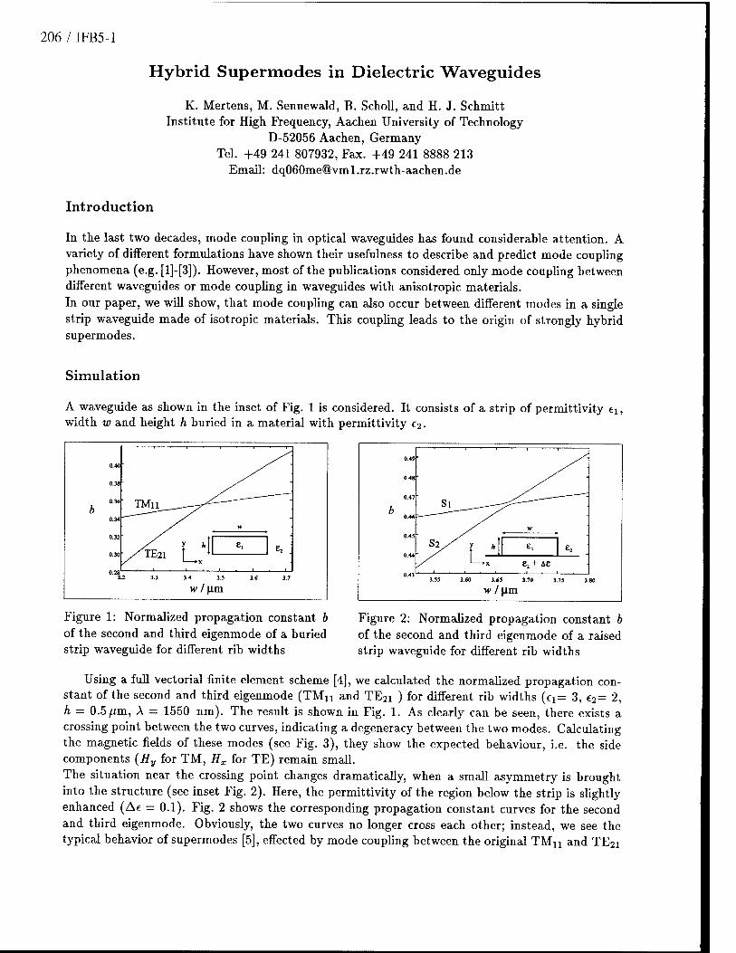
206 / IFB5-1
Hybrid Supermodes in Dielectric Waveguides
K. Mertens, M. Sennewald, B. Scholl, and H. J. Schmitt Institute for High Frequency, Aachen University of Technology
D-52056 Aachen, Germany Tel. +49 241 807932, Fax. +49 241 8888 213
Email: [email protected]
Introduction
In the last two decades, mode coupling in optical waveguides has found considerable attention. A variety of different formulations have shown their usefulness to describe and predict mode coupling phenomena (e.g. [l]-[3]). However, most of the publications considered only mode coupling between different waveguides or mode coupling in waveguides with anisotropic materials.
In our paper, we will show, that mode coupling can also occur between different modes in a single strip waveguide made of isotropic materials. This coupling leads to the origin of strongly hybrid supermodes.
Simulation
A waveguide as shown in the inset of Fig. 1 is considered. It consists of a strip of permittivity €i, width w and height h buried in a material with permittivity e2 •
i I 1 '
0.49
., , ,— | ■ | 1 T . , r-
0.4O ^
0.38 ■
0.48
b 0.3« TMii '■
0.47
b 0.46
Si
0.34 ■ : ■ """" '
0.32
0.30
0.28 3
W w
//TE21 L: e, 0.44
S3// t * c, «2 "
■ • 1—»x e2 + Ae
2 3.3 3.4 3.5 3.6 3.7 0.43 3.55 3.60 3.65 3.70 3.75 3.80
M> 1|im w/|i.m
Figure 1: Normalized propagation constant b of the second and third eigenmode of a buried strip waveguide for different rib widths
Figure 2: Normalized propagation constant b of the second and third eigenmode of a raised strip waveguide for different rib widths
Using a full vectorial finite element scheme [4], we calculated the normalized propagation con- stant of the second and third eigenmode (TMn and TE2i ) for different rib widths (ex= 3, e2= 2, h — 0.5^m, A = 1550 nm). The result is shown in Fig. 1. As clearly can be seen, there exists a crossing point between the two curves, indicating a degeneracy between the two modes. Calculating the magnetic fields of these modes (see Fig. 3), they show the expected behaviour, i.e. the side components (Hy for TM, Hx for TE) remain small.
The situation near the crossing point changes dramatically, when a small asymmetry is brought into the structure (see inset Fig. 2). Here, the permittivity of the region below the strip is slightly enhanced (Ae = 0.1). Fig. 2 shows the corresponding propagation constant curves for the second and third eigenmode. Obviously, the two curves no longer cross each other; instead, we see the typical behavior of supermodes [5], effected by mode coupling between the original TMn and TE2i

IFB5-2 / 207
mode. The magnetic field lines of these supermodes (called Si and 52 ; see Fig. 3) look totally different from the original modes. They show a very strong hybrid character with side components as strong as the main components.
• i i > > • ■ ■ i i i •
i i i / - « i i i i
i 1 1 i ■ ■ i 1 1 i i i i i • - / i i i
■ i i i • « . i i i i .
TE h\ L
.-------....
-----------
TMn
- \\\N--^/// '
\ \ \ \ \ ' / / / '
Si
v \\\v.~^^/// /
- - >. \ \ / / / y - — \ \ \ \
S2
Figure 3: Magnetic fieldlines of the second and third eigenmode of the waveguides in Fig. 1 (w = 3.45/xm) and Fig. 2 (w = 3.67 /an)
The phenomenon offers the possibility to develop new polarization sensitive devices. One exam- ple is a combined beam splitter and polarization converter as shown in Fig. 4. It consists of a mode converting section (I) and a conventional beam splitting section (II). K horizontically polarized light is launched into section I, it is converted into vertically polarized light, which can be split by the following section II. Fig. 5 helps to understand the basic principle of the device. It shows the isolines of the two super- modes in section I and their superpositions. The incoming light excites both supermodes (addition), which propagate with different velocities. At a length L^ = ■& r, both modes have a phase offset of ir to each other. Therefore, the resulting field at this point can be found by simply subtracting the two mode fields. Interestingly enough, the Hx -components almost cancel each other, so that the resulting Hy -field can be split in the following section II. For practical materials (e.g. InP) Ln lies in the 1 mm range.
The occurence of mode coupling between the two considered original modes can be described by a perturbation formulation, which will be given in our talk. To our knowledge, the phenomenom of strongly hybrid supermodes in single dielectric waveguides has not been published so far. It offers the possibility for the development of new polarization converting elements; esp. for isotropic materials. As an example, a combined beam splitter and polarization converter based on InP will be described in detail in our talk.
We thank N. Thorweihe, now with Telekom, Forschungs- und Technologiezentrum Darmstadt for letting the original FEM-program to us and helpful discussions.

208 / IFB5-3
Figure 4: Proposed combined polarization converter and beam splitter; making use of the phenomenon of hybrid supermodes
HX(S1)-HX(S2)
(i|||(|||i H^Sj) Hy(S2) H^SO + H^) JtySO-Hy^)
Figure 5: Isolines of the magnetic field for the two supermodes of the waveguide in section I (Fig. 4)
References
[1] A. Yariv, Coupled-mode theory for guided-wave optics, IEEE J. Quant. Electr., QE-9, pp. 919- 933,1973.
[2] A. Hardy and W. Streifer, Coupled-mode theory of parallel waveguides, J. Lightwave Technol., vol. LT-3, pp. 1135-1146, 1985
[3] H. A. Haus, W. P. Huang, S. Kawakami, and N. A. Whitaker, Coupled-mode theory of optical waveguide, J. Lightwave Technol., vol. LT-5, pp. 16-23, 1987
[4] B. M. A. Rahman and J. B. Davies, Penalty function improvement of waveguide solution by finite elements, IEEE Trans. Microwave Theory Tech., vol. MTT-32, pp. 922-928, 1984.
[5] P. N. Robson and P. C. Kendall (eds.), Rib waveguide theory by the spectral index method, John Wiley & Sons Inc., New York, 1990.

IFB6-1 / 209
Stable Finite Element Solutions to the Vector Wave Equation
R. Kent Smith Room 6E-316
AT&T Bell Labs, Murray Hill NJ, 07974-0636 Tel: (908) 582-7522 FAX: (908) 582-6000
One of the fundamental problems in optical electronics is the computation of the prop- agation modes of wave guide structures. For many applications, these modes may be com- puted by constructing solutions of the scalar wave equation. However, when polarization effects are important, the modes of the vector wave equation are required.
Maxwell's equations for a dielectric wave guide may be written in the following form:
V x (/i_1V x £) - k2e£ = 0 (1)
V • (e£) = 0 (2)
where k is the free space wavenumber, e and /z are the relative permittivity and permeability respectively. The appropriate boundary conditions are
€ x n = 0 : onTi (3)
V X £ X n = 0 : onT2 (4)
where the boundary has been divided into an electric wall Ty and a magnetic wall IV It is convenient to recast the curl equation , (1), into a variational form:
T(£) = ( dü{^l\V x £\2 - k2e\£\2) (5) Jo
For a comprehensive review of the methods for modal waveguide simulations see [3]. The major difficulty in solving the vector Maxwell's equations by finite element or finite
difference methods is the presence of unphysical eigenvalues. These spurious eigenvalues appear in the spectrum together with the physically correct modes. The elimination of spurious modes has been extensively discussed in the literature. Of the various formulations, the use of edge based finite elements [2, 6], appears to be the most promising. Edge elements also known as Whitney differential forms, are vectors associated with each edge in the mesh and are tangentially continuous across elements. Therefore, expanding the fields in terms of edge elements makes the fields tangentially continuous across interfaces while allowing for discontinuities in the normal component. It is precisely this feature that makes edge elements attractive for solving the vector wave equation.
The standard finite element discretization Maxwell's equations is obtained as follows [4, 5]. The electric fields vary as £(x,y,z) = E(x,y)e~,f}z. The transverse fields, Et(x,y) are expanded in terms of edge elements while the longitudinal field Ez(x,y) is expanded in terms of a nodal basis. Stationary points of equation (5) determine both the propagation constant, ß and the electric fields. The divergence equation is not discretized since solutions of equation (1) satisfy equation (2). An appropriate scaling of Ez is used to transform the quadratic eigenvalue problem into a linear eigenvalue problem, Ax = XBx where A = ß2.

210 / IFB6-2
Unfortunately, the above formulation is not free of spurious modes. The vector with components Et — 0 and Ez arbitrary are eigenvectors of equation (5) as ß —> ±oo. Clearly these solutions are unphysical since the divergence condition is not satisfied. Unless special care is taken [5], these spurious modes prohibit the uses of many standard eigenvalue solvers, such as the Lanczos method, that finds the minimum or maximum eigenvalues. These solutions may be removed by enforcing the divergence condition. The divergence condition, equation (2), may be viewed as a set of constraints that restricts the permissible solutions of the variational problem. To solve the constrained variational problem, the solution space, z, is expanded to include a set of Lagrange multipliers, p(x,y). It should be noted that this constrained variational problem is formulated in terms of the fields with Lagrange multipliers and not the vector and scalar potentials used by Bardi and Biro [1]. As with the standard treatment, the resultant equations may be recast into a linear eigenvalue problem,
Az = \Bz. (6)
With this formulation, the matrices A and B remain sparse but are much better conditioned.
In fact, the "mass matrix", B, may be permuted into a positive definite matrix. Since the largest eigenvalue of equation (6) corresponds to the lowest waveguide mode, standard sparse matrix eigenvalue methods are directly applicable. The disadvantage of expanding the space is more than offset by the computation efficiency in solving the linear eigenvalue problem.
References
[1] I. BARDI AND O. BIRO, An efficient finite-element formulation without spurious modes for anisotropic waveguides, IEEE Transactions on Microwave Theory and Techniques, 39 (1991), pp. 1133-1139.
[2] A. BOSSAVIT, Simplicial finite elements for scattering problems in electro-magnetism, Computer Methods in Applied Mechanics and Engeering, 76 (1989), pp. 299-316.
[3] K. S. CHIANG, Review of numerical and approximate methods for the modal analysis of general optical dielectric waveguides, Optical and Quantum Electronics, 26 (1994), pp. S113-S134.
[4] B. M. DILLON AND J. P. WEBB, A comparison of formulations for the vector finite ele- ment analysis of waveguides, IEEE Transactions on Microwave Theory and Techniques 42 (1994), pp. 308-316.
[5] J. F. LEE, D. SUN, AND Z. J. CENDES, Full-wave analysis of dielectric waveguides using tangential vector finite elements, IEEE Transactions on Microwave Theory and Techniques, 39 (1991), pp. 1262-1271.
[6] J. P. WEBB, Edge elements and what they can do for you, IEEE Transactions on Magnetics, 29 (1993), pp. 1460-1465.

24,1995
Rare-Earth-Doped Materials and Waveguides
IFC 1:30 pm-2:45 pm Salon 1
David L. Weidman, Presider Corning, Inc.
212 /IFCl-1
Erbium-Doped Waveguide Amplifiers and Lasers in LiNbOß
W. Sohler Angewandte Physik, Universität-GH Paderborn
Warburger Str. 100, D-33098 Paderborn
I) Introduction
In the last years there has been a growing interest in rare-earth-doped, optically pumped waveguide
amplifiers and lasers in LiNbC>3 [1,2]. In particular, erbium-doping is of major interest as it leads to
optical amplification and lasing in the wavelength range 1.52 urn < X < 1.62 urn, most important for
fiber optical communication. LiNbC>3 allows to fabricate high-quality channel guides in (locally, pho-
tolithographically defined) diffusion-doped surfaces of high erbium concentration. Moreover, LiNbC>3
has excellent electro- and acousto-optical properties allowing the development of modelocked, Q-
switched and tunable lasers. It is the aim of this contribution to review erbium-doped waveguide ampli-
fiers and lasers in LiNbC>3 with emphasis on the most recent developments and to discuss the future
potential of these devices.
II) Fabrication of Erbium-Doped Waveguides
There are different methods to fabricate erbium-doped waveguide amplifiers and lasers in LiNbC^. The
most versatile, reliable and simplest technique proved to be erbium-diffusion-doping of the LiNbC>3
surface followed by the waveguide fabrication using standard titanium-indiffusion. To obtain a deep
(~8um) Gaussian-like erbium profile of high surface concentration (~ 8-lO^cm"-') a vacuum-deposited
metallic Er- (or dielectric E^C^-) layer of about 22 ran thickness has to be indiffused during -100 h at
temperatures (~1130°C) slightly below the Curie temperature. Afterwards, photolithographically de-
fined Ti-stripes are indiffused using conventional parameters to fabricate single mode channel guides of
low scattering losses down to -0.2 dB/cm [3J.
III) Waveguide Amplifiers
Erbium-doped waveguides can be operated as optical amplifiers by pumping with sufficient power
levels. Pumping at Ap - 1480 nm is preferred to pumping at Ap ~ 980 nm, as single mode propagation
for both, pump and signal wave, can be ensured. Moreover, optical upconvcrsion and photorefractive
effects are negligible if a 1480nm pump is used. As in erbium-doped fiber amplifiers (EDFA) broad-
band gain in the wavelength range 1.52 urn < Xs < 1.62 urn can be achieved. However, the pump power
dependent absorption/gain spectrum has a more pronounced structure reflecting the energy levels of
Er3+ in the crystalline host.
Ti:Er:LiNbO"3 samples have been systematically investigated mainly as single-pass (for pump and sig-
nal) devices [4], As their length up to 70 mm is much smaller than the calculated optimum amplifier
length (which can be easily adjusted with EDFAs), a corresponding smaller gain can be expected. The
maximum value can be achieved at X.s = 1531 nm; up to 13.8 dB has been demonstrated in a single-pass
70 mm long amplifier operated with about 200 mW pump power (A.p « 1480 nm) [5], In a double-pass
(for pump and signal) device with appropriate broadband rear mirror the gain should more than double
as experimentally and theoretically proved [4].

IFCl-2 / 213
IV) Waveguide Lasers
Using Er-diffusion-doped LiNb03 amplifiers with Ti-diffused waveguides four different types of lasers
have been developed:
1. Free running Fabrv-Perot lasers
By depositing dielectric mirrors on the polished end faces of amplifier samples, Fabry-Perot type wave-
guide cavities have been built. The wavelength dependent cavity losses together with the pump power
dependent broadband gain of the Ti:Er:LiNbC>3 optical amplifiers determine the emission wavelength of
a free running laser. Thus it was possible to design and fabricate cw-lasers for six different emission
wavelengths: 1531, 1546, 1563, 1576, 1602, and 1611 nm [6,7]. Thresholds as low as 9 mW (kp *
1480 nm), slope efficiencies up to 37 % and output power levels up to 60 mW (at Pp « 210 mW) have
been achieved [5]. Moreover, fully packaged, fiber-pigtailed devices pumped by a laser diode have been
demonstrated [8].
2. Modelocked laser
By integrating a travelling-wave electrooptic phase modulator in the laser cavity FM-type modelocking
has been achieved. Suche et al. [9] reported 95 ps long pulses (detector bandwidth limited) generated at
Xs = 1532 nm with 1.4 Gflz repetition rate in a 48 mm long laser in X-cut LiNbC^. More recently,
Bosso et al. [10,11] demonstrated modelocking at Xs = 1602 nm in a 54 mm long laser of only 9 mW
threshold (X~ » 1480 nm) in Z-cut LiNbC^. Using an optical autocorrelator a pulse width of only 3.8 ps
was measured with peak power levels > 0.65 W in a special gain switched mode of operation. It was
possible to operate the diode-pumped, pigtailed and fully packaged laser not only at the cavity round-
trip frequency of 1.281 GHz, but also at higher harmonics up to 5.12 GHz.
3. Tunable laser
By integrating an acoustooptical wavelength filter in the laser cavity tunable operation has been
achieved around 1531, 1546, and 1561 nm wavelength over a total tuning range of 12 nm [12]. A sche-
matical diagram of the tunable laser is shown in Fig. 1.
polarization splitter/ TM-pass polarizer
interdigital transducers
acoustic absorbersx
Au-mirror
pump (TE-pol.)
LiNbq Ti:LiNb03 Ti:Er:LiNbq EnLiNbOj
TE-pass polarizer
broadband dielectric
mirror
signal I (TM-pol.)
Fig. 1: Schematical digram of the Er-diffusion doped acoustically tunable Ti:LiNbO3-waveguide laser; c: optical axis of LiNbC^. The total length of the laser is 54.7 mm.
214 /IFCl-3
The waveguide laser has a Fabry-Perot cavity comprised of an Au-mirror on the rear waveguide end
face and a broadband dielectric mirror as output coupler on the other side. Its key component is a mo-
nolithically integrated, active (Er-doped), double-stage, tunable wavelength filter. It consists (from left
to right in Fig. 1) of a TM-pass polarizer (polarization splitter), a first acoustooptical TM-^TE-mode
converter, a TE-pass polarizer, and a second TE^TM-converter. The pump radiation (A,p « 1480 run)
is launched into the waveguide cavity via the polarization splitter. Due to the high total round trip losses
of 6.3 dB in the first device investigated, the output power and slope efficiencies are low (< 20 uW and
< 0.02 %, respectively). The emission linewidth is 0.25 nm. The overall tuning slope is -8 nm/MHz with
a "local" tuning slope of-4 nm/MHz and sudden jumps of the emission wavelength of about 1.2 nm.
4. DBR-laser
Very recently, the first Distributed Bragg Reflector (DBR-) Ti:Er:LiNbÜ3 laser has been demonstrated
[13]. Its emission wavelength of \s = 1530.9 nm is determined by the Bragg-wavelcngth of a grating-
reflector etched into the (undoped) waveguide surface. The bandwidth of the laser emission is < 2.8
GHz; temporarily, single-frequency operation is observed. The cavity of the DBR-laser is formed by the
end-face mirror of the uncoated LiNbC>3 sample on one side and by the Bragg-grating of about 50 %
reflectivity on the other side. These low reflectivities explain the high threshold of -110 mW (A,p *
1480nm). The output power of the DBR-laser is about 2 mW if pumped by 180 mW.
V) Conclusions
Erbium-doped waveguide amplifiers and different types of lasers have been developed in LiNb03
mainly for future applications in fiber optical communications. There is still a great potential to improve
the performance of these devices. Moreover, they allow the development of a more complex monolithic
integrated optics in LiNbC>3 by combining lasers, amplifiers and further active and passive devices on
the same chip to optical circuits of higher functionality.
Acknowledgement:
The support of most of the work reported in this contribution by the European Union within the RACE-
program (EDIOLL project R2013) is gratefully acknowledged.
References: [I] E. Lallier in: "Integrated Photonics Research", OSA Techn. Digest 1993, Vol. 10, p. 348 [2] W. Sohler, Techn. Digest 5th Optoelectron. Conf, 1994, pp. 160-161, (invited) [3] I.Baumann et al., Proc. ECIO '93, 3-14 [4] R. Brinkmann et al.JEEE J. Quantum Electron. 30, 2356 (1994) [5] R. Brinkmann et al., to be published [6] R. Brinkmann et al., Electron. Lett. 27, 415 (1991) [7] P. Becker et al., Appl. Phys. Lett. 61, 1257 (1992) [8] presented at the scientific exhibitions of ECOC '92, Berlin, and ECIO '93, Neuchätel [9] H. Suche et al., Electron. Lett. 29, 1111 (1993) [10] S. Bosso et al, Proc. ECOC '94, Vol. 1. pp. 353-356 (1994) [II] H. Suche et al., submitted to Optics Letters [12] I. Baumann et al., Proc. ECOC '94, Vol. 4 (post-deadline papers), pp. 99-102 (1994) [13] J. Söchtig et al., submitted to Electron. Lett.

IFC2-1 / 215
Enhancement of 4Ii3/2 Population Inversion and Green Up-conversion of Er3+ Ions in Yb:Er:LiNbOj
Chi-hung Huang and Leon McCaughan
Department of Electrical and Computer Engineering University of Wisconsin-Madison
1415 Johnson Dr., Madison, WI 53706, USA TEL: (608) 262-0311, FAX: (608) 265-2614
The development of Er-doped fiber amplifiers and fiber lasers [1,2] has recently spawned interest in LiNb03-based integrated optic versions of these devices [3,4]. Guided wave mode- locked lasers, tunable lasers, as well as traveling wave amplifiers, have been demonstrated [5,6]. Er3+ doping concentrations and site distributions strongly affect the performance of these devices [4, 7]. Co-doping with other rare earth ions (e.g. Yb3+) to increase the useful absorbed pump power has proven useful for fiber amplifiers and lasers [8,9]. In this work we report the enhancement of the 4I13/2 level population inversion and green up-conversion of the Er ions in LiNb03 co-doped with Yb.
LiNb03 crystals uniformly doped with different concentrations of Er, Yb, and Yb:Er were grown at Tianjin University, China. The absorption spectra of single-doped Er:LiNb03 (0.7mol% Er3+) and co-doped Yb:Er:LiNb03 (0.6mol% Yb3+, 0.7mol% Er3+) for polarizations parallel and perpendicular to the z crystallographic axis (i.e. % and a polarizations, respectively) are shown in Fig. 1. Absorption at 980nm (a major pumping wavelength for Er3+ ions) is greatly enhanced for both polarizations, especially for the originally weaker 7t-polarization. Despite the presence of Yb ions, we found the lineshapes and strengths of other Er3+ absorption transitions (e.g. the 4Ii5/2 ground state to the 4Ii3/2, 4l9/2> an^ 4^9/2 manifolds) remain unchanged at room temperature.
Yb:Er:LiNbO,
Er:LiNbO,
960 980 1000 1020
^2.0 Ü
a-polarization
Yb:Er:LiNbO,
920 940 960 980
Wavelength (nm) Wavelength (nm)
Fig. 1. Absorption spectra of Er single-doped and Yb:Er co-doped LiNbOß crystals at two major polarizations at room temperature.
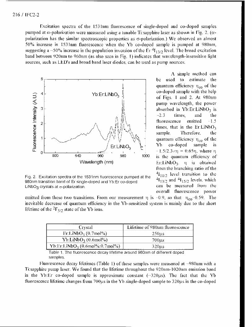
216 / IFC2-2
Excitation spectra of the 1531nm fluorescence of single-doped and co-doped samples pumped at a-polarization were measured using a tunable Ti:sapphire laser as shown in Fig. 2. ((De- polarization has the similar spectroscopic properties as a-polarization.) We observed an almost 50% increase in 1531nm fluorescence when the Yb co-doped sample is pumped at 980nm, suggesting a -50% increase in the population inversion of the Er 4I] 3/2 level. The broad excitation band between 920nm to 960nm (as also seen in Fig. 1) indicates that wavelength-insensitive light sources, such as LED's and broad band laser diodes, can be used as pump sources.
ID <
■^ 3 CO c CD
CD O c o co CD
0 3
1 -
0
I ' I ' I ' I '
Yb:Er:LiNb03 I
A
:. -AJ <4 : / EnLiNbOo \ -
be A simple method can
used to estimate the quantum efficiency r\co of the co-doped sample with the help of Figs. 1 and 2. At 980nm pump wavelength, the power absorbed in Yb:Er:LiNb03 is -2.3 times, and the fluorescence emitted -1.5 times, that in the Er:LiNbC>3 sample. Therefore, the quantum efficiency r)c„ of the
920 940 960
Wavelength (nm) 980 1000
ico Yb co-doped sample is ~1.5/2.3xr| = 0.65r|, where r\ is the quantum efficiency of Er:LiNb03. r\ is obtained from the branching ratio of the 4Iu/2 level transition to the 4I]3/2 and 4115/2 levels, which can be measured from the overall fluorescence power
emitted from these two transitions. From our measurement r\ is -0.9, so that rjco~0.59. The inevitable decrease of quantum efficiency in the Yb-sensitized system is mainly due to the short lifetime of the 2F5/2 state of the Yb ions.
Fig. 2. Excitation spectra of the 1531nm fluorescence pumped at the 980nm transition band of Er single-doped and Yb:Er co-doped LiNbC>3 crystals at a-polarization.
Ciystal Lifetime of 980nm fluorescence Er:LiNb03 (0.7mol%) 250us Yb:LiNb03 (0.6mol%) 700(.is
Yb:Er:LiNb03 (0.6mol%:0.7mol%) 320f.is Table 1. The fluorescence decay lifetime around 980nm of different doped samples.
Fluorescence decay lifetimes (Table 1) of these samples were measured at ~980nm with a Ti:sapphire pump laser. We found that the lifetime throughout the 920nm-1020nm emission band in the Yb:Er co-doped sample is approximate constant (~320u.s). The fact that the Yb fluorescence lifetime changes from 700jas in the Yb single-doped sample to 320j.is in the co-doped
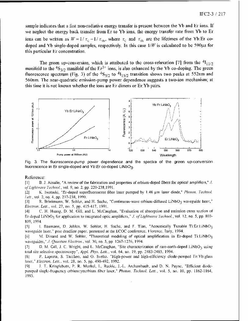
IFC2-3 / 217
sample indicates that a fast non-radiative energy transfer is present between the Yb and Er ions. If we neglect the energy back transfer from Er to Yb ions, the energy transfer rate from Yb to Er
ions can be written as W = 1 / rc -1/ r^, where TC and r^ are the lifetimes of the Yb:Er co- doped and Yb single-doped samples, respectively. In this case \IW is calculated to be 590(j.s for this particular Er concentration.
The green up-conversion, which is attributed to the cross-relaxation [7] from the 4In/2 manifold to the 4S3/2 manifold of the Er3+ ions, is also enhanced by the Yb co-doping. The green fluorescence spectrum (Fig. 3) of the 4S3/2 to
4Ii5/2 transition shows two peaks at 552nm and 560nm. The near-quadratic emission-pump power dependence suggests a two-ion mechanism; at this time it is not known whether the ions are Er dimers or Er: Yb pairs.
EnLiNbO,
Pump power at 9S0nm (AU)
540 550 560
Wavelength
570
Fig. 3. The fluorescence
fluorescence-pump power dependence and the spectra of the green up-conversion in Er single-doped and Yb:Er co-doped LiNbOß.
Reference: [1] B. J. Ainalie, "A review of the fabrication and properties of erbium-doped fibers for optical amplifiers,"./. of Lightwave Technol, vol. 9, no. 2, pp. 220-238,1991. [2] K. Iwatsuki, "Er-doped superfluorescent fiber laser pumped by 1.48 urn laser diode," Photon. Technol. Lett, vol. 2, no. 4, pp. 237-238, 1990. [3] R. Brinkmann, W. Sohler, and H. Suche, "Continuous-wave erbium-diffused LiNb03 waveguide laser," Electron. Lett., vol. 27, no. 5, pp. 415-417, 1991. [4] C. H. Huang, D. M. Gill, and L. McCaughan, "Evaluation of absorption and emission cross section of Er-doped LiNb03 for application to integrated optic amplifiers," J. of Lightwave Technol, vol. 12, no. 5, pp. 803- 809, 1994. [5] I. Baumann, D. Johlen, W. Sohler, H. Suche, and F. Tian, "Acoustically Tunable Ti:Er:LiNb03
waveguide laser," post deadline paper, presented at the ECOC conference, Florence, Italy, 1994. [6] M. Dinand and W. Sohler, "Theoretical modeling of optical amplification in Er-doped Ti:LiNb03
waveguides," J. Quantum Electron., vol. 30, no. 5, pp. 1267-1276, 1994. [7] D. M. Gill, J. C. Wright, and L. McCaughan, "Site characterization of rare-earth-doped LiNb03 using total site selective spectroscopy", Appl. Phys. Lett., vol. 64, no. 19, pp. 2483-2485, 1994. [8] P. Laporta, S. Taccheo, and O. Svelto, "High-power and high-efficiency diode-pumped Er:Yb:glass laser," Electron. Lett., vol. 28, no. 5, pp. 490-492, 1992. [91 J. T. Kringlebotn, P. R. Morkel, L. Reekie, J.-L. Archambault, and D. N. Payne, "Efficient diode- pumped single-frequency erbium:ytterbium fiber laser," Photon. Technol. Lett., vol. 5, no. 10, pp. 1162-1164, 1993.
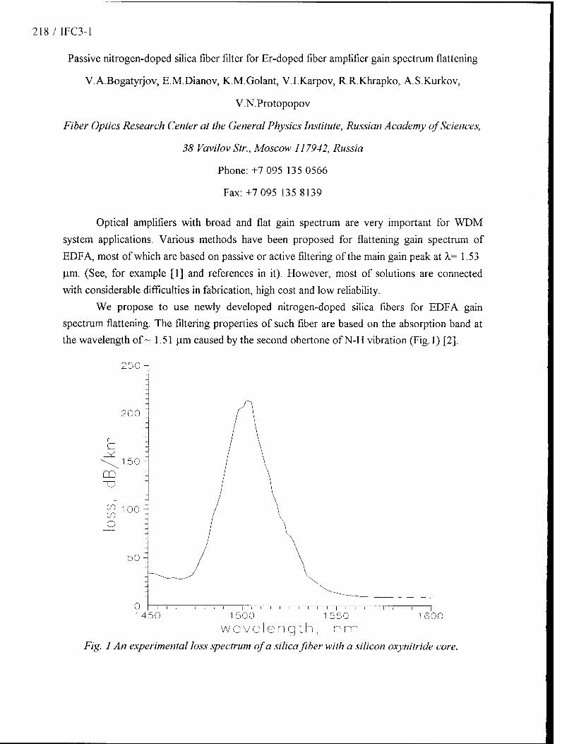
218 / IFC3-1
Passive nitrogen-doped silica fiber filter for Er-doped fiber amplifier gain spectrum flattening
V.A.Bogatyrjov, E.M.Dianov, K.M.Golant, V.I.Karpov, R.R.Khrapko, A.S.Kurkov,
V.N.Protopopov
Fiber Optics Research Center at the General Physics Institute, Russian Academy of Sciences,
38 Vavilov Str., Moscow 117942, Russia
Phone: +7 095 135 0566
Fax:+7 095 135 8139
Optical amplifiers with broad and flat gain spectrum are very important for WDM
system applications. Various methods have been proposed for flattening gain spectrum of
EDFA, most of which are based on passive or active filtering of the main gain peak at \= 1.53
p.m. (See, for example [1] and references in it). However, most of solutions are connected
with considerable difficulties in fabrication, high cost and low reliability.
We propose to use newly developed nitrogen-doped silica fibers for EDFA gain
spectrum flattening. The filtering properties of such fiber are based on the absorption band at
the wavelength of- 1.51 u.m caused by the second obertone of N-H vibration (Fig. 1) [2].
250
I I 1 | I
1500 1 600 1550 wavelength, nm
Fig. 1 An experimental loss spectrum of a silica fiber with a silicon oxynitride core.
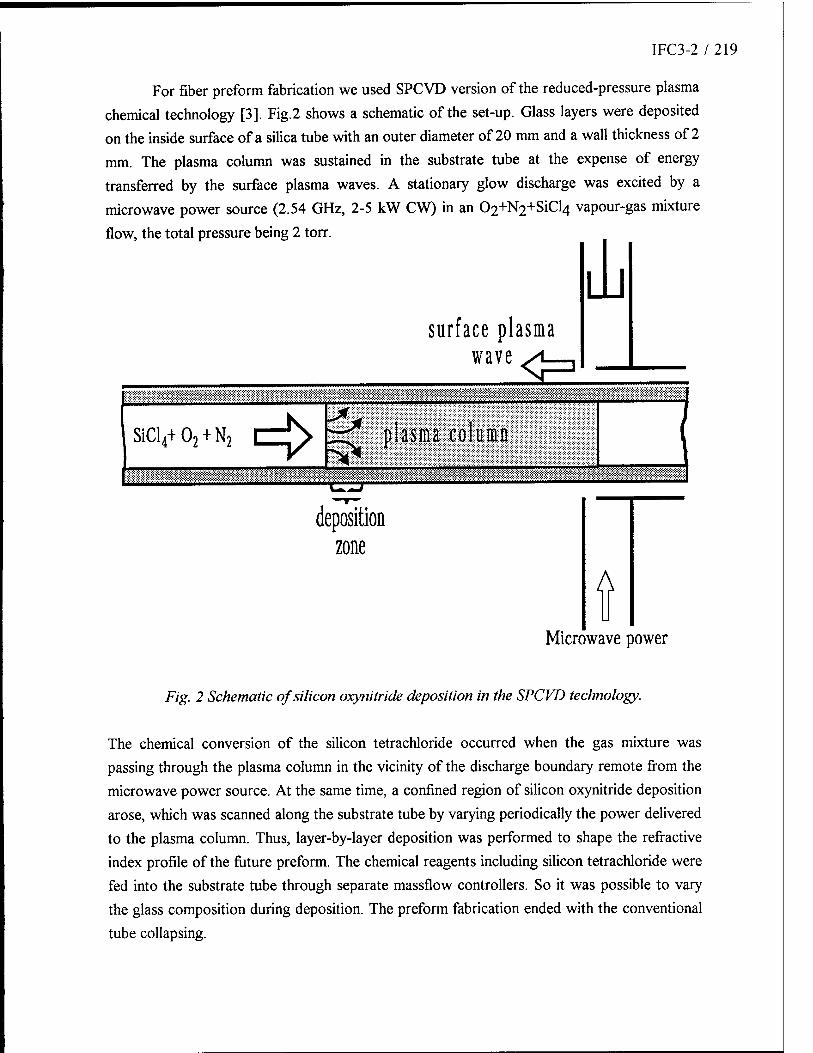
IFC3-2 / 219
For fiber preform fabrication we used SPCVD version of the reduced-pressure plasma
chemical technology [3]. Fig.2 shows a schematic of the set-up. Glass layers were deposited
on the inside surface of a silica tube with an outer diameter of 20 mm and a wall thickness of 2
mm. The plasma column was sustained in the substrate tube at the expense of energy
transferred by the surface plasma waves. A stationary glow discharge was excited by a
microwave power source (2.54 GHz, 2-5 kW CW) in an 02+N2+SiCl4 vapour-gas mixture
flow, the total pressure being 2 torr.
surface plasma wave y\—,
SiCl4+ 02 + N2 CzN
miiimmÜäm
III plasma column
LB"
deposition zone
A
Microwave power
Fig. 2 Schematic of silicon oxynitride deposition in the SPCVD technology.
The chemical conversion of the silicon tetrachloride occurred when the gas mixture was
passing through the plasma column in the vicinity of the discharge boundary remote from the
microwave power source. At the same time, a confined region of silicon oxynitride deposition
arose, which was scanned along the substrate tube by varying periodically the power delivered
to the plasma column. Thus, layer-by-layer deposition was performed to shape the refractive
index profile of the future preform. The chemical reagents including silicon tetrachloride were
fed into the substrate tube through separate massflow controllers. So it was possible to vary
the glass composition during deposition. The preform fabrication ended with the conventional
tube collapsing.

220 / IFC3-3
Fig.3 shows preliminary results of amplifier gain spectrum measurements without
filtering and with filtering using nitrogen-doped fiber. It is seen that considerable improvement
of the gain spectra has been achieved.
40
m
d
O
35-
30
25
20 1520 1540 1560
Wavelength, nm
Fig. 3. Gain spectra with (1) and without (2) N-dopedfiber filter.
References
1. E.Desurvire "Erbium-doped fiber amplifiers. Principles and Applications", John Wiley & Sons, p.480(1994).
2. V.A.Bogatyrjov, E.M.Dianov, K.M.Golant, R.R.Khrapko, A.S.Kurkov, "Silica fibers with
silicon oxynitride core fabricated by plasmachemical technology", submitted to OFC'95.
3. D.Pavy et al., in Digest of 12th European Conference on Optical Communication, Barcelona, p. 19 (1986).
IFC4-1 / 221
1.7 (im Excited State Absorption Measurement in Erbium-doped Silicate Glasses
Jose E. Roman, Chenchun Ye, and Martin Hempstead
Optoelectronics Research Centre University of Southampton
Southampton SO 17 1BJ, United Kingdom Tel. +44 703 593162, Fax. + 44 703 593149
Patrice Camy, Pascale Laborde, and Christian Lerminiaux
Corning Europe Inc. 7 bis, Avenue de Valvins
77210 Avon, France Tel. +33 1 64 69 73 87, Fax. +33 1 64 69 74 01
Planar erbium doped waveguide amplifiers are important components in the development of integrated optical communication circuits at 1.5 (im. Such devices must achieve high gains in short lengths and thus require high erbium concentrations (>1019 cm-3). At these doping levels, however, the amplifier gain and efficiency are degraded by ion-ion interactions in the form of uniform and clustered upconversion [1]. Upconversion is a problem in erbium-doped glasses because the 4/|3/2—^5/2 emission and 4IW2~^4hn ESA transitions overlap. Therefore, it is of fundamental interest to measure the ESA spectrum. Wyatt [2] measured the tail of this spectrum to demonstrate that absorption of 1.55 (im photons from the 4/13/2 level could not occur. We have
measured, for the first time, the full 1.7 (im ESA spectrum in erbium-doped glasses and used it to estimate the uniform upconversion rate. The silicate glasses studied are suitable for the development of ion-exchanged waveguide amplifiers at 1.5 |Lim.
The ESA cross section, Gesa(X), was obtained by measuring the 'gain' spectrum of an erbium-
doped waveguide in the 1.4-1.8 uxn region. In the presence of ESA, it can be shown that [2]
C-(X) = Wl In A
■NfL[üaa)+öema)]
where Nf is the effective population in the excited state (4/|3/2), L is the waveguide length, T{(X) and T0(k) are the pumped and unpumped transmission spectra, respectively, and Ga(k)
and Geni(k) are the 1.5 |im absorption and emission cross-sections, respectively. Equation 1
neglects the wavelength dependence of Nf under the assumption that the signal mode profile does not change appreciably over the wavelength range of interest. Ga(X) was obtained from absorption measurements, while the relative shape of Gem(k) was obtained from the 1.5 fim

222 / IFC4-2
fluorescence spectrum [3]. The two unknowns, N"" and the peak value of onil(X), were
determined by fitting the function W(k) = Af L[au(X) + oi,m(X)] to the measured 'gain',
ln(7J(A,)/7^,(X)), in the wavelength region where there is no ESA. The residual difference
revealed the ESA spectrum.
Figure 1 shows the experimental apparatus used in the 'gain' measurement. Thallium-exchanged waveguides were fabricated in our silicate glasses. A white light source provided the signal and a 980nm TkSapphire served as the pump. Figure 2 shows the measured 'gain1, ln(7^(A,)/7^(A,)),
and the fitted function, W(k), for one of the glasses studied: a barium silicate, CorningE Figure
3 shows the ESA spectrum obtained by subtracting the curves in figure 2, as well as the emission cross section spectrum. Table 1 shows the peak emission, o"an, and ESA, G"CSU, cross sections
obtained from the fit for Corning 1 and Corning2, an aluminoborosilicate for which plots are not shown.
Using the measured emission and ESA cross section spectra, we estimated the uniform upconversion rate for the glasses. Uniform upconversion in 1.5 |im erbium amplifiers is represented theoretically by a -C(N2)
2 term in the rate equations for the excited population, N2
[1], where C is the uniform upconversion rate. In the kinetic limit [4] of high erbium concentration, high inversion levels, and fast energy migration rates, it can be shown that [4,5]
(27i) irRn J
where c is the speed of light, /; is the index of refraction, and Ro is the minimum distance
between erbium ions. Table 1 shows the calculated upconversion constants for Corning 1 and 2 using n = 1.5 and Rn =0.46 nra. The latter value was approximated as twice the sum of the ionic
radii of oxygen and erbium. For an erbium concentration, No, of 5x 10'1) enr- and a lifetime, I, of
15 ras, a C value of 8x10¹⁹ cmVs will cause a lifetime decrease of approximately (l-CA^x) =40%. Since similar decreases have been measured for silicate glasses [6], the
calculations appear to predict the correct order of magnitude for uniform upconversion.
In conclusion, we have measured the 1.7 (im ESA spectra for various erbium-doped silicates,
which together with the emission spectra, define the 1.5 ,11111 upconversion process. By comparing the spectral overlap between the emission and ESA cross sections for various glasses, it should be possible to predict and compare their uniform upconversion rates. Therefore, the ESA measurement can serve as a useful spectroscopic tool in the selection of erbium-doped glasses for 1.5 jim waveguide amplifiers. Other glasses are currently under study.
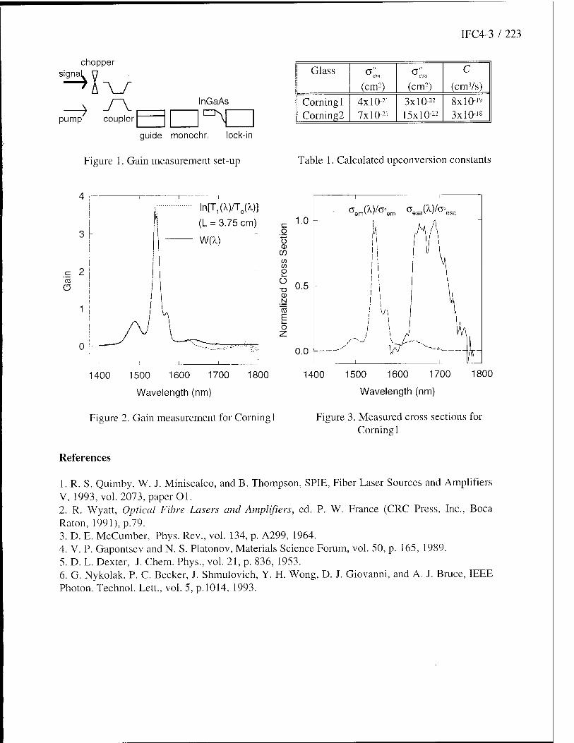
IFC4-3 / 223
chopper Signa
InGaAs
pump coupler ^A guide monochr. lock-in
Figure 1. Gain measurement set-up
Glass a" em
(cm2)
a" esa
(cm2)
C
(cmVs)
Corning 1 Corning2
4x10⁻²' 7x10⁻²'
3x10-22 15x10-22
8xl0-19
3xlO-18
Table 1. Calculated upconversion constants
f ! !
i IntT/^/T^)]
3 \ (L = 3.75 cm) c
o W(A,) o
ni w
■1 2 CO
CD
1 - J I : w w o Ü T3 0 N
15 E s_
o z
0
i ! I I
1400 1500 1600 1700 18 00
Wavelength (nm)
Figure 2. Gain measurement for Corning 1
1400 1500 1600 1700
Wavelength (nm)
1800
Figure 3. Measured cross sections for Corningl
References
1. R. S. Quimby, W. J. Miniscalco, and B. Thompson, SPIE, Fiber Laser Sources and Amplifiers V, 1993, vol. 2073, paper 01. 2. R. Wyatt, Optical Fibre Lasers and Amplifiers, ed. P. W. France (CRC Press, Inc., Boca Raton, 1991), p.79. 3. D. E. McCumber, Phys. Rev., vol. 134, p. A299, 1964. 4. V. P. Gapontsev and N. S. Platonov, Materials Science Forum, vol. 50, p. 165, 1989. 5. D. L. Dexter, J. Chem. Phys., vol. 21, p. 836, 1953. 6. G. Nykolak, P. C. Becker, J. Shmulovich, Y. H. Wong, D. J. Giovanni, and A. J. Bruce, IEEE Photon. Technol. Lett., vol. 5, p. 1014, 1993.

224 / NOTES

Friday, February 24, 199.
Modeling of Waveguide Devices
IFD 1:30 pm-3:00 pm Salon 4
S. K. Chaudhuri, Presider University of Waterloo, Canada

226 / IFDl-1
Analysis of integrated optical Waveguide Structures with arbitrary curved Interfaces by using the Method of Lines
W. D. Yang and R. Pregla Allgemeine und Theoretische Elektrotechnik
FernUnivcrsität, Hagen 58084 Hagen
Telephone: +49 2371 566 256 Fax: +49 2371 51898
1. Introduction
A modified Method of Lines for analyzing integrated optical layered and cylindrical waveguide structures with arbitrary curved interfaces is presented. The structures are shown in Fig. 1 and Fig. 2 for layered waveguide and in Fig. 3 for cylindrical waveguide. Because in each layer or region the refractive index is uniform, so only the Helmholtz equation is needed to solve. The method is full wave analysis for 3D in Cartesian and cylindrical coordinates, respectively. Therefore most complicated structures in the optical domain can be analyzed very well with this method. As examples a rib waveguide and a Bragg grating waveguide are chosen. The results arc in good agreement with that in [1] and [3].
IF Layered Waveguide
\ c 1
■■ IV ' 1
III d
II
1 X ^
— Jiz
■ , ,
Fig. 1 Cross Section of layered Waveguide Fig. 2 Waveguide structure with integrated gratings in longitudinal direction
Because each layer or region has the uniform refractive index, hence the fields must satisfy the Helmholtz equation
V24> + crk2
0i>= o (i)
where ib stands for Ez{ri„Hz). The discrctized and transformed Helmholtz equation in Cartesian coordi- nates leads
d2ib '---'■ n (2)
dy k-yij) = 0
and its solution is
where
-ip = cosh(kgy)A + sinh(fcy?y)£?
fe2 ™ k2k2
\i=hZ2TZ1PxTx
fc~- = iz (g> A; + A; ®IX~ eriTZ
\2.=h7'2T71P,Tr
(3)
(4)
and Ix and Iz are the unit matrices in x and z-dircction respectively[2]. Ixz = IX®IZ is the unit matrix in the xz plane. Px and Pz are difference operators in x and z-dircction, respectively, which are defined in [2] and [1]. According to the reference [2] there is following relations between interface A and B in the original domain
HB
V z Y V
EA
HA

IFD1-2 / 227
i/ith F = [T.diag(TÄ,Te)]r
[T-ä-1]fe 2-A-1r
Y = -[T-a-L]A-iT
.y ~ - f = dmg(Te,Th)
and the point multiplication means that [A ■ B]ik = AikBik and
[r]ik = cosh[kykdi(v)] [a-1]ik = kyk smh[kykd~i(v)]
with v = x for 2D problems and */ = x, z for 3D problems. According to [2]
HA — —YAEA
the similar formula is given from eq.(5) in the original domain as follows
HB = -YBEB YB = (Y + VYA)(V + ZYA)-1
To match the tangential fields on the matching faces which are curved lines for 2D case or curved faces for 3D case (A or B in the Fig. 1) the tangential fields must be calculated as follows
(10)
(6)
(7)
(8)
(9)
Hi — TXCHX TyCtly Tzr.Hz
Et = TXCEX + TyCEy + TZCEZ (11)
with TXC = diag(cosari) , ryc = diag(cosayi) and TZC = diag(cos azi), where axi, ayi and azi are the
angles between x, y or z and the tangential face of point i, respectively, and a„- + ayi = —. For 2D
problems TZC = 0. and cosar!- = smayi and vice versa. After some algebraic procedures of matching the tangential fields on the matching faces one obtains the system equation as follows
R{l)FM = 0 (12)
where FM is the tangential field matrix on the matching face and R(i) is the coefficient matrix which includes the implicit propagation constants 7 and 7 = a + jß where a is loss and ß is phase of the fileds.
III. Cylindrical Waveguide
As shown in Fig. 3 the lateral section of cylindrical waveguide is described and the longitudinal direc- tion of the structure is shown in Fig. 2. The princi- ple shown in [6] for microstrip structures can also be used for the optical structures, some modifications are introduced here. First the hybrid mode is con- sidered and second the length of the discretized lines can be zero or oo(i.e r = 0 and r —> 00) and third the periodic variation in the propagation direction of the waveguide is analyzed. Generally speaking the lateral section of the circular(n = 2) and rect- angular (n —> 00) form can be taken as elliptical form described by following equation
a 0 (13)
The discretized and transformed Helmholtz equa- tion in cylindrical coordinates is given as follows.
Id d(f> 2
--r(r-r-) + (fcr r dr ar ^)* = ° (14)
kliere <f> stands for Ez(rj0Hz) and Fig. 3 Lateral section of cylindrical waveguides
(15) Av,= ¥ N - the number of the discretization lines
A^ is described in the above subsection and Pv is defined the same as Pz as a — 1[1].
k2r = erk
20I - X2
Z
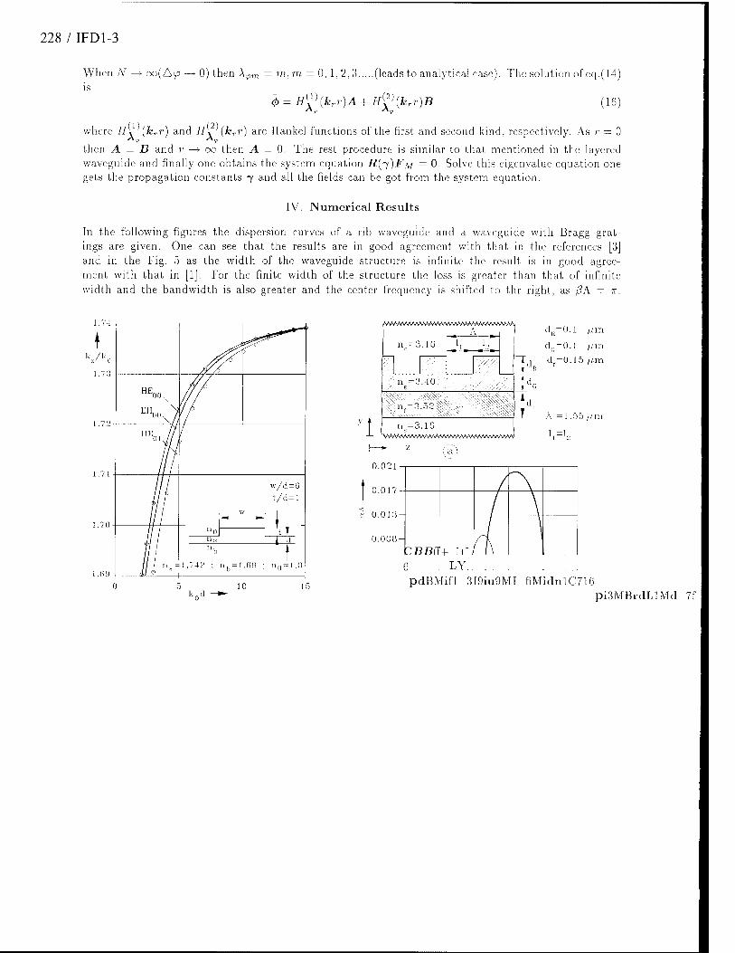
228 / IFD1-3
When Ar
is co(Aip —* 0) then Xvm = m, m = 0, 1, 2, 3 (leads to analytical case). The solution of eq.(14)
r(i) (2), <f> = H{''{krr)A + H\rJ(krr)B ;i6)
where II[ (krr) and Il[ (krr) are Hankel functions of the first and second kind, respectively. As r = 0
then A = B and r —► oo then A = 0. The rest procedure is similar to that mentioned in the layered waveguide and finally one obtains the system equation R{*y)FM = 0. Solve this eigenvalue equation one gets the propagation constants 7 and all the fields can be got from the system equation.
IV. Numerical Results
In the following figures the dispersion curves of a rib waveguide and a waveguide with Bragg grat- ings arc given. One can see that the results are in good agreement with that in the references [3] and in the Fig. 5 as the width of the waveguide structure is infinite the result is in good agree- ment with that in [1]. For the finite width of the structure the loss is greater than that of infinite width and the bandwidth is also greater and the center frequency is shifted to thr right, as /3A = IT.
1.74 (V^\^A\W^^AAV*VA^WtWAWA^WAV^^i
A
'I
n =3.1ü
a n =3.-10;
; 11.=3.52$
n =3.16 s VWMVAVMVAVM»M\WvWMV.Vj
d =0.1 //111
dG = 0.1 jim
"TJ d =0.15 /./in
A =1.55 /.an
1,=1.,
CBBn+ rn/ 6 . LY pdBMifl 3I9iu9MI fiMidnlC716
pi3MBrdLlMd 7f
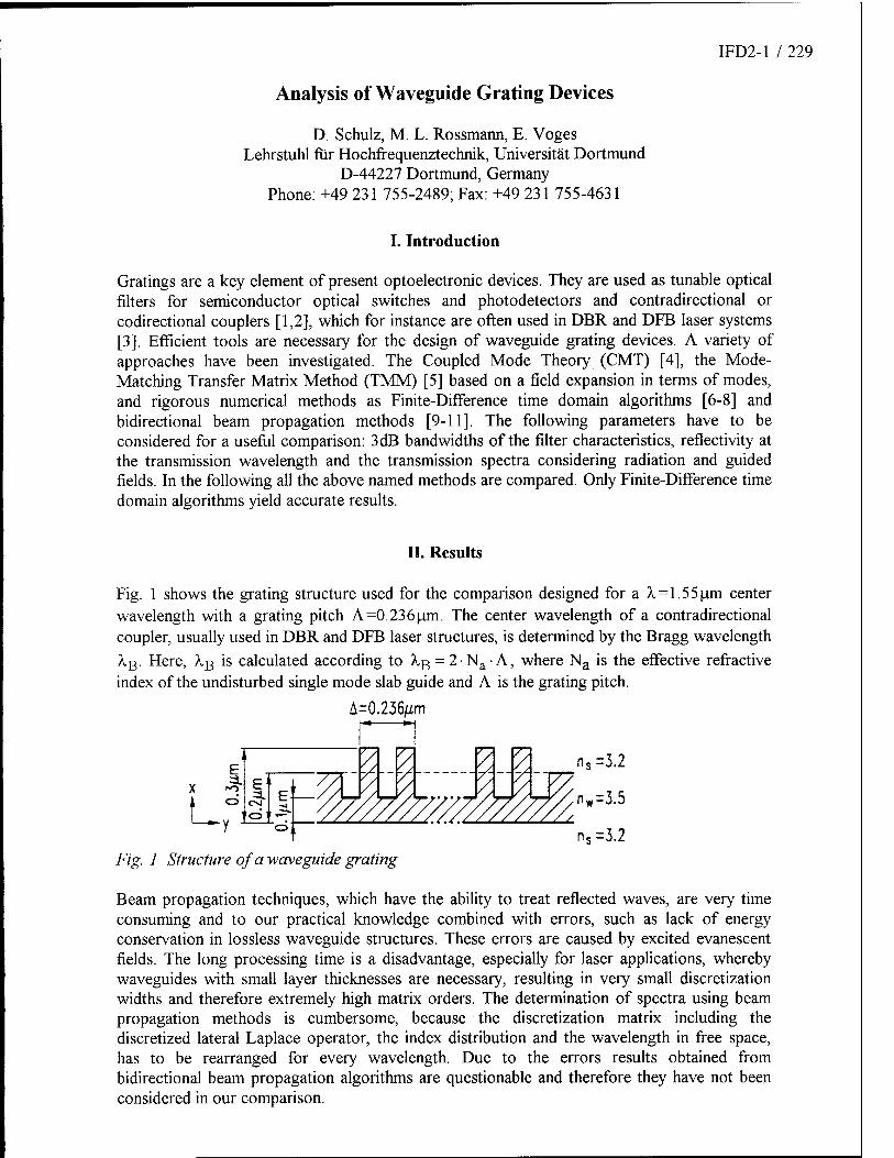
IFD2-1 / 229
Analysis of Waveguide Grating Devices
D. Schulz, M. L. Rossmann, E. Voges Lehrstuhl fur Hochfrequenztechnik, Universität Dortmund
D-44227 Dortmund, Germany Phone: +49 231 755-2489; Fax: +49 231 755-4631
I. Introduction
Gratings are a key element of present optoelectronic devices. They are used as tunable optical filters for semiconductor optical switches and photodetectors and contradirectional or codirectional couplers [1,2], which for instance are often used in DBR and DFB laser systems [3]. Efficient tools are necessary for the design of waveguide grating devices. A variety of approaches have been investigated. The Coupled Mode Theory (CMT) [4], the Mode- Matching Transfer Matrix Method (TMM) [5] based on a field expansion in terms of modes, and rigorous numerical methods as Finite-Difference time domain algorithms [6-8] and bidirectional beam propagation methods [9-11]. The following parameters have to be considered for a useful comparison: 3 dB bandwidths of the filter characteristics, reflectivity at the transmission wavelength and the transmission spectra considering radiation and guided fields. In the following all the above named methods are compared. Only Finite-Difference time domain algorithms yield accurate results.
H. Results
Fig. 1 shows the grating structure used for the comparison designed for a Ä=1.55 urn center wavelength with a grating pitch A=0.236u,m. The center wavelength of a contradirectional coupler, usually used in DBR and DFB laser structures, is determined by the Bragg wavelength X-Q. Here, A,B is calculated according to A,B = 2-Na-A index of the undisturbed single mode slab guide and A is the grating pitch
A=0.236/im
where Na is the effective refractive
7\ YÄ ns=3.2
nw=3.5
ns =3.2 Fig. 1 Structure of a waveguide grating
Beam propagation techniques, which have the ability to treat reflected waves, are very time consuming and to our practical knowledge combined with errors, such as lack of energy conservation in lossless waveguide structures. These errors are caused by excited evanescent fields. The long processing time is a disadvantage, especially for laser applications, whereby waveguides with small layer thicknesses are necessary, resulting in very small discretization widths and therefore extremely high matrix orders. The determination of spectra using beam propagation methods is cumbersome, because the discretization matrix including the discretized lateral Laplace operator, the index distribution and the wavelength in free space, has to be rearranged for every wavelength. Due to the errors results obtained from bidirectional beam propagation algorithms are questionable and therefore they have not been considered in our comparison.

230 / IFD2-2
Time Domain propagation algorithms allow to simulate the propagation of pulses and have the general advantages of full vectorial formulation, calculation of transmission characteristica in one step, and the automatic and accurate inclusion of reflections. For this reason the time domain method is used as a reference method.
Fig. 2 depicts the bandwidth of the reflection spectrum for the above mentioned methods and Fig. 3 shows the reflectivity at the transmission wavelength both dependent on the number of used grating pitches. Despite the short calculation time the results from the standard coupled mode theory deviates from the reference method by approximately 40%. The values for the maximum reflectivity agree with the results from the time domain method for grating devices with more than 300 grating pitches. For long grating devices with more than 30 grating pitches the reflectivity values and the 3dB bandwidths calculated by the Mode-Matching Transfer Matrix Method coincide very well with the reference method. This Mode-Matching Transfer Matrix Method considers the fundamental mode in each waveguide section. In case the Mode- Matching Transfer Matrix Method additionally includes the first radiation mode, the reflectivity values approach the reference values. The approach can be further optimized when the number of radiation modes is increased.
From the calculated transmission spectra (Fig. 4) we conclude that the transmission spectra calculated by the Coupled Mode Theory and Mode-Matching Transfer Matrix Method based on the fundamental modes do not include radiation modes, and they do not yield useful results for the transmission spectra. The transmission spectra determined by the Mode-Matching Transfer Matrix Method can be improved by considering additional radiation modes.
III. Conclusion
In practice Coupled Mode Theory and Mode-Matching Transfer Matrix Method can be used for a first estimation of the device behaviour, only. For an accurate design of waveguide grating devices numerical tools as Finite-Difference time domain methods are necessary.
50 100
Number of grating pitches —►
Fig. 2 Bandwidths obtained for different methods dependent on the number of grating pitches
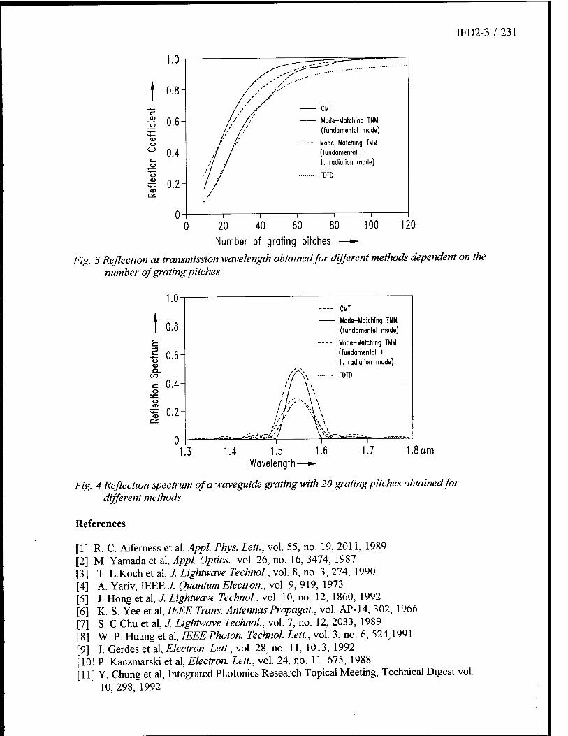
IFD2-3 / 231
tu o o
_o o
03
1.0-
0.8
■5 0.6
0.4
£ 0.2-
0
CMT
Mode-Motching TMM
(fundamental mode)
Mode-Matching TMM
(fundamental +
1. radiation mode)
0 100 120 20 40 60 80
Number of grating pitches —»►
Fig. 3 Reflection at transmission wavelength obtained for different methods dependent on the number of grating pitches
1.0-1 —- CMT
t 0.8- Mode-Matching TMM
(fundamental mode)
E Mode-Matching TMM
£ O.fi- (fundamental + -£ U.U
1. radiation mode)
1/1 ,y "N\ FDTD
«= 0.4- i 1 \ \ _o i 1 \\ o a> r \ >
=5 0.2- w 0 _££i^~- "**-'" "1 1 ' l"
1.3 1.4 1.5 1.6 1.7 1. Wavelength-
1.8/xm
Fig. 4 Reflection spectrum of a waveguide grating with 20 grating pitches obtained for different methods
References
[I] R. C. Alferness et al, Appl. Phys. Lett, vol. 55, no. 19, 2011, 1989 [2] M. Yamada et al, Appl. Optics., vol. 26, no. 16, 3474, 1987 [3] T. L.Koch et al, J. Lightwave Techno!., vol. 8, no. 3, 274, 1990 [4] A. Yariv, IEEE J. Quantum Electron., vol. 9, 919, 1973 [5] J. Hong et al, J. Lightwave Techno!, vol. 10, no. 12, 1860, 1992 [6] K. S. Yee et al, IEEE Trans. Antennas Propagat, vol. AP-14, 302, 1966 [7] S. C Chu et al, J. Lightwave Techno!, vol. 7, no. 12, 2033, 1989 [8] W. P. Huang et al, IEEE Photon. Techno! Lett, vol. 3, no. 6, 524,1991 [9] J. Gerdes et al, Electron. Lett, vol. 28, no. 11, 1013, 1992 [10] P. Kaczmarski et al, Electron. Lett, vol. 24, no. 11, 675, 1988 [II] Y. Chung et al, Integrated Photonics Research Topical Meeting, Technical Digest vol.
10, 298, 1992

232 / IFD3-1
Overview of Quantum Wires for Optical Devices
J.N. Schulman Hughes Research Laboratories
Malibu, CA 90265
Techniques for fabricating semiconductor quantum wires continue to proliferate and improve, yielding shrinking dimensions and clearer evidence for the sought after quantum confinement effects. However, practical application of quantum wires in optical devices requires that stringent demands must be fulfilled. It is not obvious how soon this will occur. This talk will discuss basic concepts involved in potential optical devices utilizing quantum wires, and how they relate to the goal of achieving practical devices.
Some of the applications which will be discussed include
semiconductor lasers, non-linear materials, and optical modulators. Purely electronic devices have also been proposed and will be briefly surveyed. The main issue in all proposed devices is growth and fabrication uniformity. The results of the analytical tools which have been applied to analyzing quantum wire quality, especially photoluminescence spectroscopy, will be discussed relative to the theoretical expectations. This will focus on electronic energy level splitting due to lateral confinement and polarization dependent effects.
The quantum wire laser is presently the most obvious promising application, and will be discussed in detail. Comparison of quantum well and wire lasers will be made. The advantages of both of these structures (low threshold current, temperature insensitivity, etc.) are primarily attributed to the concentration of the electronic density of states in energy space. Therefore, in some ways the advantages of quantum wires follow from those of quantum wells, but differences do exist. It will be shown, for example, that strain effects, valence band mixing, and Auger effects in quantum wires are not just extrapolations of quantum well behavior.
The review will finalize with a discussion of the ultimate goals of quantum confined laser structures, the three-dimensional quantization of both electronic and optical modes - quantum dots and microcavity lasers.

IFD4-1 / 233
Cubic and Quadratic Dispersion Compensation using In-Fiber Bragg Gratings.
J. A. R. Williams N. J. Doran I. Bennion
Department of Electronic Engineering and Applied Physics, Aston University, Aston Triangle, Birmingham, B4 7ET, UK.
Tel: +44-21-3593611 x 4961. Fax: +44-21-3590156
1 Introduction
In fibre optic transmission systems quadratic dispersion compensation may be achieved with dispersion profiling schemes using fibers of differing dispersions [1]. Since the first observation of photo-induced refractive index changes in optical fibers, and the subsequent capability of manufacturing in-fiber Bragg gratings [2] there has been much interest in application of such gratings for dispersion compensation, particularly in fibre optic transmission systems. It has been shown that a linearly chirped Bragg grating used in reflection has particular potential in this area as it has (approximately) a constant dispersion over bandwidths sufficient to support ultra-short pulses [3]. Such gratings have been demonstrated in a variety of dispersion compensation and pulse compression applications [4, 5]. The problem of cubic disprsion compensation is not easily addressed with fibre dispersion profiling schemes as the cubic dispersion in silica is always positive at communication wavelengths. In this paper we show that both quadratic and cubic dispersion compensation may be achieved using practical quadratically chirped gratings. We derive the design equations for such gratings, give some particular design examples and discuss some of the issues involved with using them as dispersion compensation elements.
2 Analysis The grating model we propose for quadratic and cubic dispersion compensation has a sinusoidal mod- ulation in the effective refractive index along its length of the form
6n(z) = sin(K(z)z) K(z) = a0 + y z + yz2 (1)
a0,ai and a2 are the coefficients to be determined. For a grating of length Lg, -Lg/2 < z < Lg/2. Differentiating K(z)z w.r.t. z gives the instantaneous frequency k{z) of the structure along its length, and from this we obtain an expression for position z along the grating as a function of the Bragg reflected wavelengthA.
z(X) = -—— ± A~2 JXaj - 4Ao2a0 + 16a27rn (2) 2(22 V
We assume that the gratings are highly chirped and that the coupling coefficient of the grating is large. In this case we can consider that the light be reflected from a single point in the grating given by the expression 2 above, and that it will be unaffected by the remainder of the grating where it is off resonance. In this case we can simply write the group delay D\ of the light reflected from the chirped grating as the distance traveled by the light divided by its group velocity £>i = 2(n/c)z(A) Sequentially differentiating with respect to wavelength gives the quadratic group delay dispersion D2 and cubic group delay dispersion D3 terms as follows.
D2 = ^ r (3) c\2 (Xal - 4Aa2a0 + 16a27rn)2
±16n27T (Aa? - 4Aa2a0 + 12a27rn) D3 = —-—— r- (4)
cA2 (Aa2 - 4Aa2ao + 16a27rn)2
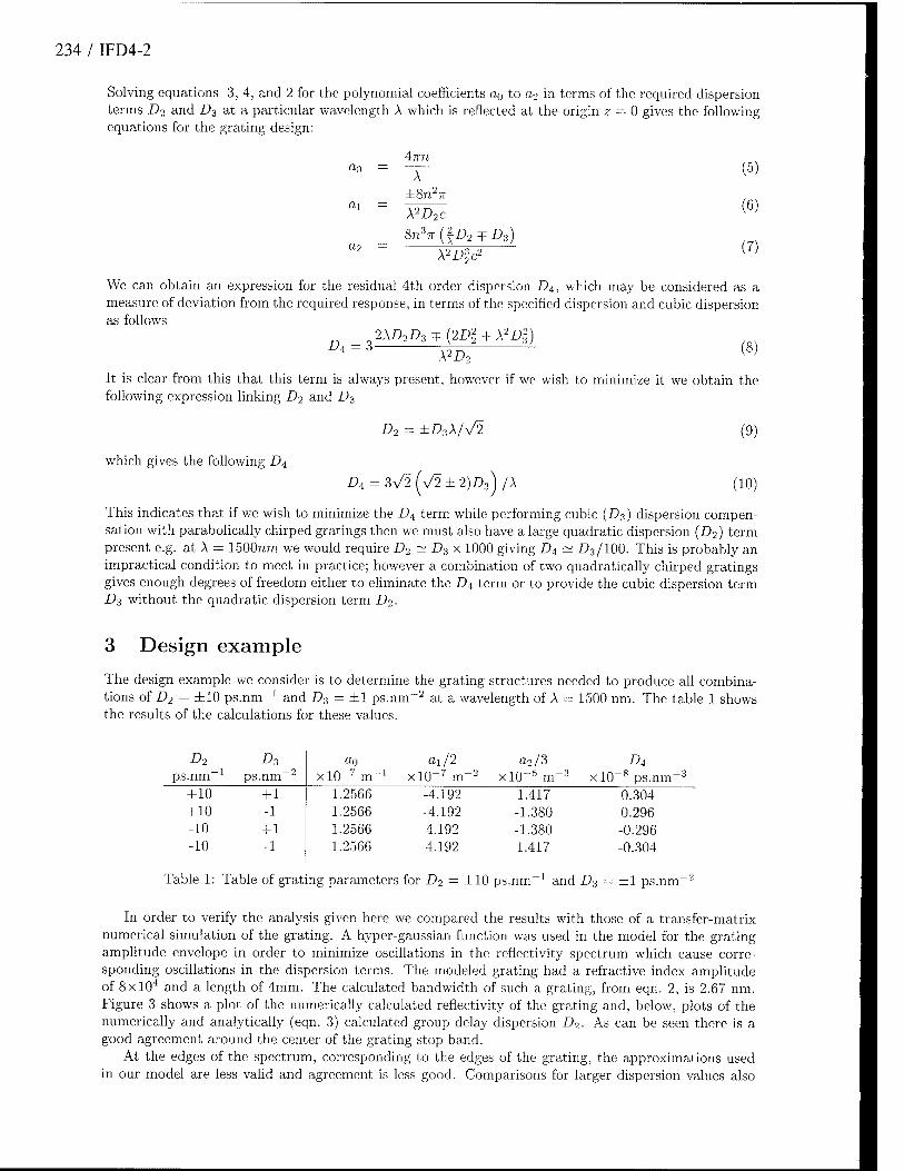
234 / IFD4-2
Solving equations 3, 4, and 2 for the polynomial coefficients a0 to a2 in terms of the required dispersion terms D2 and D3 at a particular wavelength A which is reflected at the origin z = 0 gives the following equations for the grating design:
47m ao = ~Y~ (5) ±8n27T
a'2 ~ Ä^Dp (7)
We can obtain an expression for the residual 4th order dispersion D4, which may be considered as a measure of deviation from the required response, in terms of the specified dispersion and cubic dispersion as follows
o2XD2D3^(2Dl + X2Dl) Di = 3 X^D2
(8)
It is clear from this that this term is always present, however if we wish to minimize it we obtain the following expression linking D2 and D3
which gives the following D4
D2 = ±D3X/V2 (9)
D4=3V2(V2±2)D3'Sj /\ (10)
This indicates that if we wish to minimize the D4 term while performing cubic (D3) dispersion compen- sation with parabolically chirped gratings then we must also have a large quadratic dispersion (£>2) term present e.g. at A = 1500nm we would require D2 ~ D3 x 1000 giving D4 ~ D3/100. This is probably an impractical condition to meet in practice; however a combination of two quadratically chirped gratings gives enough degrees of freedom either to eliminate the D4 term or to provide the cubic dispersion term D3 without the quadratic dispersion term D2.
3 Design example
The design example we consider is to determine the grating structures needed to produce all combina- tions of D2 = ±10 ps.nm-1 and D3 = ±1 ps.nm-2 at a wavelength of A = 1500 nm. The table 1 shows the results of the calculations for these values.
D2 £3 a0 ai/2 a2/3 D4 ps.nm-1 ps .nm~2 xlO-7 m-1 xlO-7 m-2 xlO-6 m-3 xlO ~8 ps.nm-3
+ 10 + 1 1.2566 -4.192 1.417 0.304 + 10 -1 1.2566 -4.192 -1.380 0.296 -10 + 1 1.2566 4.192 -1.380 -0.296 -10 -1 1.2566 4.192 1.417 -0.304
Table 1: Table of grating parameters for D2 = ±10 ps.nm 1 and D3 = ±1 ps.nm-2
In order to verify the analysis given here we compared the results with those of a transfer-matrix numerical simulation of the grating. A hyper-gaussian function was used in the model for the grating amplitude envelope in order to minimize oscillations in the reflectivity spectrum which cause corre- sponding oscillations in the dispersion terms. The modeled grating had a refractive index amplitude of 8xl04 and a length of 4mm. The calculated bandwidth of such a grating, from eqn. 2, is 2.67 nm. Figure 3 shows a plot of the numerically calculated reflectivity of the grating and, below, plots of the numerically and analytically (eqn. 3) calculated group delay dispersion D2. As can be seen there is a good agreement around the center of the grating stop band.
At the edges of the spectrum, corresponding to the edges of the grating, the approximations used in our model are less valid and agreement is less good. Comparisons for larger dispersion values also
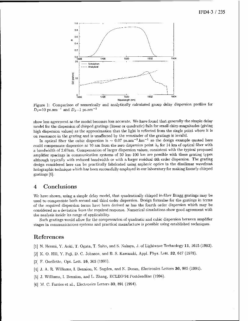
IFD4-3 / 235
1.0
0.8
0.6
0.4 -
0.2 -
0.0 1496
20 1500
a io
Simulation Analytical
1504 1496 1498 1500 1502 Wavelength (nm)
Figure 1: Comparison of numerically and analytically calculated group delay dispersion profiles for D2=10 ps.nm-1 and D3=l ps.nm-2
show less agreement as the model becomes less accurate. We have found that generally the simple delay model for the dispersion of chirped gratings (linear or quadratic) fails for small chirp magnitudes (giving high dispersion values) as the approximation that the light is reflected from the single point where it is on resonance in the grating and is unaffected by the remainder of the gratings is invalid.
In optical fiber the cubic dispersion is ~ 0.07 ps.nm-3.km-1 so the design example quoted here could compensate dispersion at 10 nm from the zero dispersion point A0 for 14 km of optical fiber with a bandwidth of 2.67nm. Compensation of larger dispersion values, consistent with the typical proposed amplifier spacings in communication systems of 50 km-100 km are possible with these grating types although typically with reduced bandwidth or with a larger residual 4th order dispersion. The grating design considered here can be practically fabricated using aspheric optics in the dissilimar wavefront holographic technique which has been successfully employed in our laboratory for making linearly chirped gratings [6].
4 Conclusions
We have shown, using a simple delay model, that quadratically chirped in-fiber Bragg gratings may be used to compensate both second and third order dispersion. Design formulae for the gratings in terms of the required dispersion terms have been derived as has the fourth order dispersion which may be considered as a deviation from the required response. Numerical simulations show good agreement with the analysis inside its range of applicability.
Such gratings would allow for the compensation of quadratic and cubic dispersion between amplifier stages in communications systems and practical manufacture is possible using established techniques.
References
[1] N. Henmi, Y. Aoki, T. Ogata, T. Saito, and S. Nakaya, J. of Lightwave Technology 11, 1615 (1993).
[2] K. O. Hill, Y. Fuji, D. C. Johnson, and B. S. Kawasaki, Appl. Phys. Lett. 32, 647 (1978).
[3] F. Ouellette, Opt. Lett. 16, 303 (1991).
[4] J. A. R. Williams, I. Bennion, K. Sugden, and N. Doran, Electronics Letters 30, 985 (1994).
[5] J. Williams, I. Bennion, and L. Zhang, ECLEO'94 Postdeadline (1994).
[6] M. C. Farries et al., Electronics Letters 30, 891 (1994).
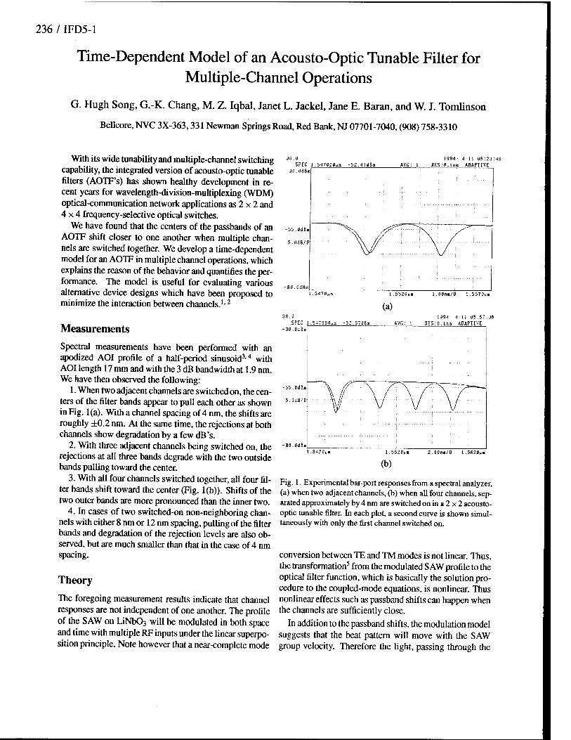
236 / IFD5-1
Time-Dependent Model of an Acousto-Optic Tunable Filter for Multiple-Channel Operations
G. Hugh Song, G.-K. Chang, M. Z. Iqbal, Janet L. Jackel, Jane E. Baran, and W. J. Tomlinson
Bellcore, NVC 3X-363,331 Newman Springs Road, Red Bank, NJ 07701-7040, (908) 758-3310
With its wide tunability and multiple-channel switching capability, the integrated version of acousto-optic tunable filters (AOTF's) has shown healthy development in re- cent years for wavelength-division-multiplexing (WDM) optical-communication network applications as 2 x 2 and 4x4 frequency-selective optical switches.
We have found that the centers of the passbands of an AOTF shift closer to one another when multiple chan- nels are switched together. We develop a time-dependent model for an AOTF in multiple channel operations, which explains the reason of the behavior and quantifies the per- formance. The model is useful for evaluating various alternative device designs which have been proposed to minimize the interaction between channels.1,2
Measurements
Spectral measurements have been performed with an apodized AOI profile of a half-period sinusoid3,4 with AOI length 17 mm and with the 3 dB bandwidth at 1.9 nm. We have then observed the following:
1. When two adjacent channels are switched on, the cen- ters of the filter bands appear to pull each other as shown in Fig. 1(a). With a channel spacing of 4 nm, the shifts are roughly ±0.2 nm. At the same time, the rejections at both channels show degradation by a few dB's.
2. With three adjacent channels being switched on, the rejections at all three bands degrade with the two outside bands pulling toward the center.
3. With all four channels switched together, all four fil- ter bands shift toward the center (Fig. 1(b)). Shifts of the two outer bands are more pronounced than the inner two.
4. In cases of two switched-on non-neighboring chan- nels with either 8 nm or 12 nm spacing, pulling of the filter bands and degradation of the rejection levels are also ob- served, but are much smaller than that in the case of 4 nm spacing.
Theory
The foregoing measurement results indicate that channel responses are not independent of one another. The profile of the SAW on LiNb03 will be modulated in both space and time with multiple RF inputs under the linear superpo- sition principle. Note however that a near-complete mode
JO.O SPEC 1 .547820,,
-30.0dBn AVC: 1 RES
1994- : 0.1 na
-55.0dE
5.0dB/D
ao.odB«
30.0
SPEC -3O.0d2
4-11 05:23: ADAPTIVE
1.5470»» 1 ,5520I,II
(a)
1.00il»/D 1.5570««
1994- 4-11 05:57:3 1 .547960um -52.57dBo AVC: 1 RES:0.1nn ADAPTIVE
2.00nn/D 1.5620»
(b)
Fig. 1. Experimental bar-port responses from a spectral analyzer, (a) when two adjacent channels, (b) when all four channels, sep- arated approximately by 4 nm are switched on in a 2 x 2 acousto- optic tunable filter. In each plot, a second curve is shown simul- taneously with only the first channel switched on.
conversion between TE and TM modes is not linear. Thus, the transformation5 from the modulated SAW profile to the optical filter function, which is basically the solution pro- cedure to the coupled-mode equations, is nonlinear. Thus nonlinear effects such as passband shifts can happen when the channels are sufficiently close.
In addition to the passband shifts, the modulation model suggests that the beat pattern will move with the SAW group velocity. Therefore the light, passing through the

IFD5-2 / 237
CD
£: norm, wavenumber 0 5 10
0 12 3 4 channel spacing [498 GHz/Div., -4 nm/Div.]
ca
t: norm, wavenumber 0 5 10
0 12 3 4 channel spacing [498 GHz/Div., -4 nm/Div.]
Fig. 2. Calculated switching spectral responses of an acousto- optic tunable filter with the half-period sinusoid acousto-optic interaction profile of length 17 mm when two adjacent chan- nels are switched together. Solid curve: Time-averaged bar-port response. Dash-dot curve: Time-averaged cross-port response. Dashed curves: Worst-case responses for the two ports over one beat period. Dotted curves: Responses for the two ports when only the first channel is switched on. The scale £ explicitly shows the distance of the adjacent channel with respect to the 3-dB bandwith of the filter.
AOI region, sees one of the many variations of a moving AOI profile at different times. The whole response then fluctuates at the difference frequencies of input RF's, e.g., ~ 500 kHz, and their harmonics due to the nonlinear ef- fect.
Model for Multiple-Channel Operation All the above mentioned effect can be explained by a suit- able model of the time-dependent complex coupling coef- ficient or the AOI profile. For any original AOI profile of a complex quasi-static function qi(z) and for TV operating channels, the ultimate coupling coefficient is found to be
N
q(z,t)='£sjqi(z)ezp[-ifä-R)z + iajt + i9j], 7'=l
(1) where Qj is a random variable for each RF input phase, and 9(j and ßy are the SAW propagation constant and fre- quency, respectively. The parameter Sj is either 1 or 0 de- pending on switching of the v'th channel.
Suppose that the AOI profile has the form of a half- period sinusoid,3 q\{z) = Q\Tl(z/L\ — l/2)sin(nz/Li), with IT(;c) = 1 for |jt| < 1/2 or 0 otherwise, with Q\ be- ing a constant and L\ = 17 mm, which was approximately realized for the measurement of Fig. 1. The solution to the coupled-mode equations with this AOI profile is shown in Fig. 2. All the essential features of the measurements can be confirmed with this calculated plot and a similar one with four switched-on channels. The dashed curves
Fig. 3. Spectral responses of an acousto-optic filter with the reduced-sine profile of (2) with Li = 34 mm. The 3-dB band- width is found to be 230.1 GHz or 1.848 nm. Two adjacent channels are switched on by two corresponding copropagating SAW's. Individual curves are identified as in Fig. 2.
representing the maximum values over the beat period of 2n/(Cl2 -ßi) ~ 2 JAS are important for the prediction of worst-case crosstalk from the oscillating spectral re- sponses of the filter.
Suppose that we have an AOI profile whose shape is of a reduced sinusoid:6
<72(z) =
02 sin(27tz/L2), rQ2 sin(2nz/L2) 0,
0<z<L2/2, L2/2<z<L2, otherwise,
(2)
where Q2 is an appropriate amplitude constant, L2 is the total AOI length of 34 mm, and r is the optimized ampli- tude reduction factor around 0.17. The technique imple- menting this profile was described in Ref. 6. The plot with a similar channel selection condition as the case of Fig. 2 are shown in Fig. 3. Note that, while the rejection level has been degraded, the usable channel bandwidth has been in- creased.
Model for Counterpropagating Surface Acoustic-Waves It was demonstrated2 that the undesirable nonlinear effects discussed in the foregoing section can be significantly re- duced by reducing the overlap in a symmetric structure of the reduced-sine profile. This was achieved by inject- ing the SAW's of the adjacent channels in the opposite di- rection, so that those two SAW's counterpropagate. The SAW's were launched to the 4-, -, +, —z directions for four individual optical channels in an alternating fashion by two interdigitial transducers. The worst case happens when all four channels are switched on. The model for time-varying coupling coefficient for this case is found to be
q(z,t) = <?2(z)exp(iß1f + i01)

238 / IFD5-3
+ <72(L-z)exp[-i(32-3G)z-in2f + i02] + <72(z)exp[-i(%-3G)z + iQ3? + ie3]
+ <^(L-z)exp[-i(3Q,-9G)z-ia,? + ie4],
(3)
where parameters for fabrication inaccuracies are ignored. The beating in this case is different from the previous case of copropagating SAW's. When two adjacent channels are switched on simultaneously, the AOI profile beats with period 27t/(Qi +Ü2) — 2.9 ns. When three consecutive channels are switched on, the acoustic wave at any one point will be a combination of two beats, the first of which has the above beat period at 2.9 ns and the other of which is 2 n/ (O3 - Qi) ~ 1 (is for channel spacing of 4 nm. Then the light response will fluctuate at these primary frequen- cies and, to the second-order, at sum/difference frequen- cies from the nonlinear effect.
With the model AOI profile of (2), the calculated spec- tral responses from the simulation for the situation are given in Fig. 4, Unlike the case of two channels switched on, the case with more than two switched-on channels re- quires a stochastic analysis, since the random process be- comes nonergodic. The spectral responses with all four channels being switched on are shown as several curves in Fig. 4(b). Note that the worst case would hit -7.5 dB for the copropagating case (not shown) instead of -13 dB in Fig. 4(b). This simulation study strongly suggests that, in order to achieve the desired crosstalk level7 of better than -35 dB under the current physical limit of the LiNbÜ3 technology, a dilation scheme8 along with the counter- propagating scheme is necessary.
In summary, we have developed a time-dependent model of an AOTF for multiple-channel operations for both cases of SAW's copropagating and counterpropgat- ing. The model has correctly given quantitative expla- nation of passband shifts and the degradation of the re- jection levels. The time-averaged amount of the shift in an AOTF with the copropagating SAWs has been found to be largely determined by the ratio between the chan- nel distance and the 3-dB bandwidth. The model has also quantified the fluctuation of the spectral responses for the various cases of multiple-channel operations, which has been found to be in good agreement with our recent exper- iments. Experimental observations of the temporal modu- lation were reported in Ref. 9.
References
1 G.H. Song, to be published in Appl.Opt., 33, no. 31(1994). 9
2 J. L. Jackel, J. E. Baran, G.-K. Chang, M. Z. Iqbal, D. Fritz, and R. Ade, submitted for IEEE Photon. Tech. Lett. (1994).
3 D. A. Smith and J. J. Johnson, IEEE Trans. Ultrasonics, Fer- roelectrics, Frequency Control, 40, 22(1993).
f: norm, wavenumber 0 5 10
0 12 3 4 channel spacing [498 GHz/Div., -4 nm/Div.]
(a) £: norm, wavenumber
0 12 3 4 5 channel spacing [498 GHz/Div., —4 nm/Div.]
(b)
Fig. 4. Spectral responses of an acousto-optic filter with the reduced-sine profile of (2) with L2 = 34 mm. (a) Two adja- cent channels are switched on with counterpropagating SAW's. (b) Four surface-acoustic waves are counter-propagating in the (-| 1—) fashion. Individual curves are identified as in Fig. 2.
J. E. Baran, D. A. Smith, and A. d'Alessandro, Conf. on Optical Fiber Commun., 1994 Tech. Dig. Ser. Vol. 4 (OSA, Washington, D. C, 1994), pp. 57-58.
G. H. Song, J. Opt. Soc. Am. A, 11, 2027 (1994).
J. L. Jackel, J. E. Baran, A. d'Alessandro, and D. A. Smith, to be published in IEEE Photon. Tech. Lett. (1994).
E. L. Goldstein and L. Eskildsen, submitted for IEEE Pho- ton. Tech. Lett. (1994).
K. Padmanabhan and A. N. Netravali, "Dilated networks for photonic switching," IEEE Trans. Commun., COM-35, 1357(1987).
M. M. Choy, K. W. Cheung, D. A. Smith, and J. E. Baran, IEEE Photon. Tech. Lett., 1, 171(1989).
February 24, 1 995
Robust, Stable, and Manufacturable Optoelectronic Technology
IFE 3:30 pm-5:00 pm Salon 1
Ian R. Croston, Presider Integrated Optical Components
240 / IFEl-1
Hybrid Micropackaging for Optoelectronic Multi-Chip Modules
J. P. Hall, M. J. Goodwin, G. Glynn, M. Q. Kearley, A. J. Moseley, and J. R. Rawsthorne
GEC-Marconl Materials Technology, Caswell, Towcester, Northants, NN12 8EQ, United Kingdom, ++44 1327 350581.
Optoelectronic Multi-Chip Modules
Hybrid integration of optoelectronic and electronic components to form multi-chip modules provides a route to the cost-effective fabrication of high-performance devices for avionics, datacomms and fibre-to- the-home applications. The hybrid approach allows the choice of the most appropriate technology for the fabrication of each sub-component; e.g. GaAs or InP based lasers or detectors, Si or GaAs integrated circuits, low-loss silica waveguides. Careful design is required, however, for the mounting of devices to ensure that the optical and electrical performance is not impaired. A hybrid micropackaging scheme may need to address some or all of the following issues: stable and efficient optical interfacing between detector, laser or LED and fibre or waveguide; provision of low-loss waveguides for optical signal routing or processing; provision of laser driver and receiver circuits with impedance-matched interconnect for data input/output, dc interconnect and ground plane for screening. Efficient heat dissipation from active components must also be considered. In many optoelectronic modules the accurate positioning and fixing of the optical fibre in a critical alignment to the optoelectronic chip dominates the assembly and packaging costs. For wider deployment of optoelectronic modules, it is thus desireable to use a packaging scheme that reduces the cost of the fibre interfacing operation, by passive alignment of components. Silicon, now used for electronic multi-chip module carriers, is also a good choice for optoelectronic hybrid modules, offering a good expansion match to InP and GaAs, acceptable thermal conduction, the formation of microetched features such as accurate V-grooves for fibre location^1) and is compatible with the fabrication of silica-on-silicon waveguides.
Silicon Baseplate Fabrication for Passive Fibre Interfacing
Microfabrication techniques have been used to produce piece-parts of sufficient accuracy that alignment is automatic, i.e. not requiring the device to be powered up during the assembly sequence. The key to ims technique is the fabrication of baseplates for locating fibres in V-grooves aligned to the chip moimiing position. Standard photolithography and etch processes arc used to pattern a silicon oxide im1:;]- layer on the wafer aligned parallel to the 1*10 flat of a 100 orientai.ion wafer then an nnisotrnpic v.,-:-, etch (iyöy^l'y potassium hydroxide in propan-2-o!) is used to fabricate recesses and V-groovcs. The slow-e'icr'ng 111 planes form the sidewalis of V-grooves, permitting a self-limiting etch process. Sub-micrornelre fabrication accuracies can be achieved for V-grcoves for fibre nosiiionmg. The etching of the sihacm hs either performed late in the process flow, requiring careful proiecnor or interconnect metallisation and dielectric layers against the aggressive eichanf, or early in the process, using a process that is toVmnt oT the presence of deep-etched features.
The silicon baseplate processing includes steps to form solder-weitable pads, accurately aligned to the V- grooves. The solder-wettable pads are surrounded by a non-wcttable dielectric region and a controlled volume of solder is deposited by evaporation onto each pad. Before mounting the devices, also prepared with corresponding arrangements of solder-wettable pads carefully aligned to the active region, the solder is reflowed to form solder bumps. When the device chip is offered up for bonding, this flip-chip bonding process relies on the surface tension of molten solder between solder-wettable areas on the chip and chip carrier pulling the chip into position from an initial approximate alignment, as the bond is formed (Figure 1). Positioning accuracies of the order of ~1 pm have been achieved (2).
Hybrid Micropackaging Scheme.
The hybrid micropackaging approach being developed and exploited at GMMT combines the electronic circuits - LED and laser drive circuits, receiver circuits and associated electrical interfaces - with the

IFE1-2 / 241
optoelectronic devices and associated input/output fibres, on a single silicon carrier. In the datalink applications discussed below, additional waveguide routing components are not required. The key elements in the passive fibre interfacing scheme selected here are microetched silicon components for chip carriers with V-grooves for passive fibre positioning and flip-chip solder bump technology for chip positioning and electrical interfacing. This technology is being applied to packaging discrete and array LEDs, detectors, lasers and optoelectronic integrated circuits (OEICs); one example is discussed in more detail below.
Hybrid Micropackaging for a High-Speed Transceiver Module.
Silicon package components have been fabricated for optoelectronic modules for interconnecting processor boards in avionic equipment on an optical backplane. The need for a rugged, compact unit containing a laser with drive circuitry, and a detector with receiver circuitry for burst-mode transmission of data at 600 Mbit/s over ~1 metre has been addressed using a silicon baseplate for alignment of the laser to 50 }im core multimode fibre as well as for electrical interconnection, with the module lid and spacer to clear internal components ("picture-frame")(Figure 2) also fabricated in silicon. The laser/fibre alignment is estimated to need an accuracy of <±20 urn to give the required performance; a similar accuracy is required for the detector/fibre alignment. The laser, selected for good high-temperature operation, is mounted on a controlled thickness of solder (3) on a metal pad defined photolithographically in registration with the fibre- locating groove (Figure 3); coupling efficiencies of 10% - 20 % are achieved without the use of lenses. The photodiode detector is mounted in a recess of defined depth in the baseplate, and a fibre with a 45° bevelled reflector end is used to couple light to the detector with ~ 1 dB excess loss measured. Conventional thin-film metallisation and dielectric processing steps are used to form the electrical interconnections in the hybrid multi-chip module. The "picture-frame" spacer is fabricated by etching through 630 um thick silicon; this is soldered to the baseplate to seal the fibres in position. Once the lid has been positioned, separate electrically screened compartments are formed for the transmit and receive functions. The unit is completed by soldering on a metal lead-frame for surface-mount. Figure 4 shows a transceiver prior to lid fixing and encapsulation. The encapsulated module is 3 mm by 15 mm by 25 mm in size. Operation at 600 Mb/s over a backplane link has been demonstrated; the transmit power was +2 dBm, and, using a custom ECL receiver chip in the module a sensitivity of -27 dBm and a dynamic range of 20 dB were measured.
Conclusions.
The passive-aligned interfacing of LEDs, lasers and detectors to multimode and singlemode optical fibres, and the hybrid integration of electronic circuits using microfabricated silicon components provides a route to compact packages with reduced assembly costs. These components will give increased penetration of optoelectronic devices in telecoms and datacoms applications.
Acknowledgements.
This work has been carried out with the support of GEC businesses and the EC in the ESPRIT III Project 6276 HOLICS (Hierarchical Optical Interconnects for Computer Systems) and RACE R2073 OMAN (OEIC Modules for the Access Network) programmes. The authors would also like to acknowledge the contribution of Jörg Wieland of the Swiss Federal Institute of Technology, Zurich, with his work on ECL receiver circuits.
References
[1] K.E. Petersen, "Silicon as a mechanical material," Proc. IEEE, 70(5), pp 420-457, 1982.
[2] MJ. Wale and C. Edge, "Self-aligned flip-chip assembly of photonic devices with electrical and optical connections," IEEE Trans. Components, Hybrids and Manuf. Technol, 13(4), pp 780- 786, 1990.
[3] C. Edge, R.M. Ash, G.G. Jones and M.J. Goodwin, "Flip-chip solder bond mounting of laser diodes," Electron. Lett., 27(6), pp 499-501, 1991.
242 / IFE1-3
wettable pads
(1) - initial coarse alignment
Figure 1. Solder bump reflow
"KE^ (2) - solder reflow (3) - chip pulled
into position
Silicon Lid
Picture Frame
Silicon Baseniaie
':MZM3
Figure 3. Fibre in V-groove, aligned to laser
Figure 2. Micro-etched silicon package
Figure 4. Partly-assembled hybrid-micropackaged transceiver module
IFE2-1 / 243
Environmentally Rugged 2.5Gbit/s Lithium Niobate Modulators for Volume Manufacture
A.C. O'Donnell, J. Dodson, C. Reynolds & P. Jiang
Integrated Optical Components Ltd, 3 Waterside Business Park,
East ways, Witham, Essex, CM8 3YQ, United Kingdom.
Lithium niobate based integrated optical components have been the subject of major research & development over the past decade. Whilst the perfomance, integration and functionality have improved dramatically their deployment in commercial systems has been limited by the need to establish environmentally rugged components in volume manufacture. In developing our 2.5Gb/s modulator for OC-48/STM-16 applications our goal has been to establish compliance with Bellcore requirements!1! which defines initial envi- ronmental criteria together with routine quality control and environmental activities. The approach adopted employs a unique, highly compact, surface-mount package for lithium niobate circuits, as shown in figure 1, with kovar body and multi-layer ceramic feedthroughs. This allows us to achieve low cost volume manufacture and direct PCB mounting together with conventional chip mounting and bonding techniques which further enhance the volume manufacture potential. In addition, by careful selection of attaching epoxies and adjusting the assembly methodolgy , stress related effects on bias voltage stability are eliminated!2!, which whilst not covered by Bellcore severely affect the system performance of the components. The optical feed-throughs employ our patented hermetic or near-hermetic assemblies t3l to provide a compliant joint for minimising the effects of thermal expansion mismatch between lithium niobate chip and package. This approach has allowed significant sav- ings in the time required for pigtailing and assembly in volume manufacture. In addition we have been able to employ both standard and polarisation maintaining fibres without degradation. The later has not been reported to our knowledge as a feed-through in an hermetic package. This in conjunction with conventional lid seam-sealing defines the basis of our approach.
The modulators have been subjected to the standard battery of tests including vibration, mechanical shock and temperature cycling. The results of ten modulators cycled through -40 °C to +80°C are plotted in figure 2. In addition components have been sub- jected to additional 'operational' tests such as biased humidity wherein the modulators are subject to the Bellcore 80°C/85% RH test but under applied voltage, as shown in figure 3. To date components have operated for 1700 hours, results to 5000 hours will be presented at the conference. These components are currently being evaluated in order to define activation energies, lifetime and MTTF data. Beyond the mechanical tests additional operational tests have been made, eg 300g shock during operation with <0.5dB loss variation during pulse. Full results of all such tests will be presented.
244 / IFE2-2
This 'modular' packaging approach has now been integrated into new product lines such as a 10Gb/s modulator employing the same surface mount footprint. In this manner future product integrations will be significantly closer to Bellcore compliance than previous introductions. In addition, initial results available to date indicate that the cur- rent -50°C to +85°C temperature range may be extended to -50°C to +125°C thereby meeting military standards.
The authors should like to thank Dieter Hundreiser and Rob Taylor of Northern Tele- com for many discussions and comments together with guidance through the Bellcore specifications.
References.
[1]
[2]
[3]
TA-NWT-001385, 'Generic requirements for optoelectronic devices in fibre optic systems', Bellcore, (1993).
A.C O'Donnell et al. 'Environmental and electrical stability of lithium niobate integrated optical modulators', to be published.
Patent application
Figure 1. An IOC 2.5Gb/s lithium niobate modulator
IFE2-3 / 245
Insertion Loss Change / dB 1
Temperature
0.5 -
-0.5
Figure 2. Insertion loss change of ten IOC 2.5Gb/s modulators through thermal cycling -40C to +80C
Insertion Loss, dB 12
11.5
11 -
10.5
10
9.5
8.5
••
• •-
J L 200 400 600 800 1,000
time(hr) 1,200 1,400 1,600 1,800
Figure 3. An IOC modulator subjected to 80C/85% RH with +5V applied to the bias port Stability of +/-0.5dB of its original value, to 1700hrs is evident.
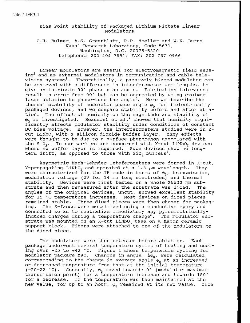
246 / IFE3-1
Bias Point Stability of Packaged Lithium Niobate Linear Modulators
C.H. Bulmer, A.S. Greenblatt, R.P. Moeller and W.K. Burns Naval Research Laboratory, Code 5671,
Washington, D.C. 20375-5320 telephone: 202 404 7591; FAX: 202 767 0966
Linear modulators are useful for electromagnetic field sens- ing1 and as external modulators in communication and cable tele- vision systems2. Theoretically, a passively-biased modulator can be achieved with a difference in interferometer arm lengths, to give an intrinsic 90° phase bias angle. Fabrication tolerances result in error from 90° but can be corrected by using excimer laser ablation to phase-tune the angle3. Here we describe the thermal stability of modulator phase angle <pQ for dielectrically packaged devices, and we compare stability before and after abla- tion. The effect of humidity on the magnitude and stability of 0Q is investigated. Beaumont et al.4 showed that humidity signi- ficantly affects modulator stability under conditions of constant DC bias voltage. However, the interferometers studied were in Z- cut LiNb03 with a silicon dioxide buffer layer. Many effects were thought to be due to a surface phenomenon associated with the Si02. In our work we are concerned with X-cut LiNb03 devices where no buffer layer is required. Such devices show no long- term drift, as opposed to those with Si02 buffers
5.
Asymmetric Mach-Zehnder inteferometers were formed in X-cut, Y-propagating LiNb03 and operated at a 1.3 /im wavelength. They were characterized for the TE mode in terms of 0O, transmission, modulation voltage (2V for 14 mm long electrodes) and thermal stability. Devices were first tested on a whole 25x30 mm sub- strate and then remeasured after the substrate was diced. The angles of the original devices, uncut, showed excellent stability for 15 °C temperature increases. Most devices on diced pieces remained stable. Three diced pieces were then chosen for packag- ing. The Z-faces were metallized using a conductive epoxy and connected so as to neutralize immediately any pyroelectrically- induced charges during a temperature change6. The modulator sub- strate was mounted on an X-cut LiNb03 base on a Macor ceramic support block. Fibers were attached to one of the modulators on the diced piece.
The modulators were then retested before ablation. Each package underwent several temperature cycles of heating and cool- ing over -2 5 to +4 2 °C. Figure 1 shows temperature cycling for modulator package M9c. Changes in angle, A0O, were calculated, corresponding to the change in average angle 0Q at an increased or decreased temperature from that at the initial temperature (~20-22 °C) . Generally, cpQ moved towards 0° (modulator maximum transmission point) for a temperature increase and towards 180° for a decrease. If the temperature was then maintained at the new value, for up to an hour, 0n remained at its new value. Once
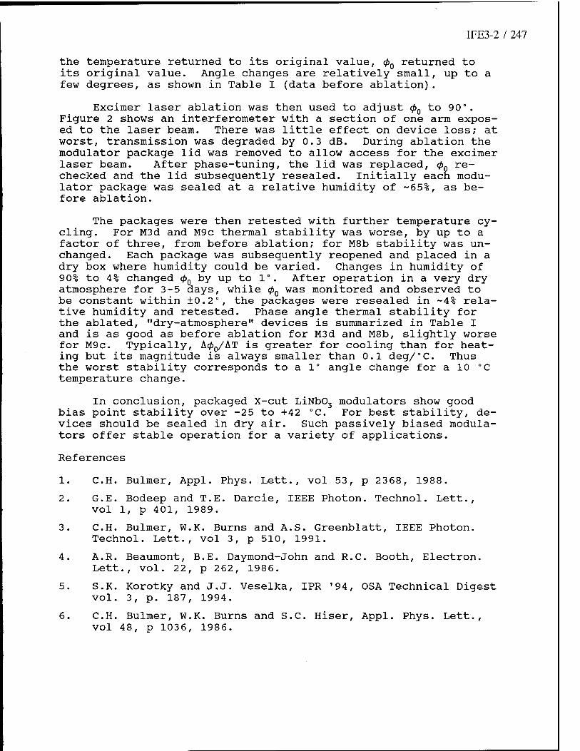
IFE3-2 / 247
the temperature returned to its original value, 0O returned to its original value. Angle changes are relatively small, up to a few degrees, as shown in Table I (data before ablation).
Excimer laser ablation was then used to adjust 0O to 90°. Figure 2 shows an interferometer with a section of one arm expos- ed to the laser beam. There was little effect on device loss; at worst, transmission was degraded by 0.3 dB. During ablation the modulator package lid was removed to allow access for the excimer laser beam. After phase-tuning, the lid was replaced, 0O re- checked and the lid subsequently resealed. Initially each modu- lator package was sealed at a relative humidity of -65%, as be- fore ablation.
The packages were then retested with further temperature cy- cling. For M3d and M9c thermal stability was worse, by up to a factor of three, from before ablation; for M8b stability was un- changed. Each package was subsequently reopened and placed in a dry box where humidity could be varied. Changes in humidity of 90% to 4% changed 0O by up to 1°. After operation in a very dry atmosphere for 3-5 days, while 0O was monitored and observed to be constant within ±0.2°, the packages were resealed in ~4% rela- tive humidity and retested. Phase angle thermal stability for the ablated, "dry-atmosphere" devices is summarized in Table I and is as good as before ablation for M3d and M8b, slightly worse for M9c. Typically, A0o/AT is greater for cooling than for heat- ing but its magnitude is always smaller than 0.1 deg/°C. Thus the worst stability corresponds to a 1° angle change for a 10 °C temperature change.
In conclusion, packaged X-cut LiNb03 modulators show good bias point stability over -25 to +42 °C. For best stability, de- vices should be sealed in dry air. Such passively biased modula- tors offer stable operation for a variety of applications.
References
1. C.H. Bulmer, Appl. Phys. Lett., vol 53, p 2368, 1988.
2. G.E. Bodeep and T.E. Darcie, IEEE Photon. Technol. Lett., vol 1, p 401, 1989.
3. C.H. Bulmer, W.K. Burns and A.S. Greenblatt, IEEE Photon. Technol. Lett., vol 3, p 510, 1991.
4. A.R. Beaumont, B.E. Daymond-John and R.C. Booth, Electron. Lett., vol. 22, p 262, 1986.
5. S.K. Korotky and J.J. Veselka, IPR '94, OSA Technical Digest vol. 3, p. 187, 1994.
6. C.H. Bulmer, W.K. Burns and S.C. Hiser, Appl. Phys. Lett., vol 48, p 1036, 1986.
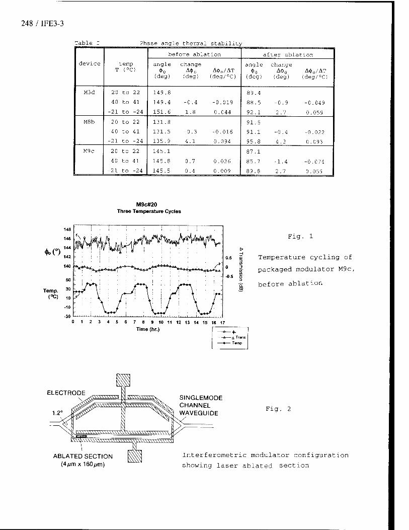
248 / IFE3-3
Table I Phase angle thermal stability
device T
;emp (°C)
bef ore ablation a fter ablation
angle <t>0
(deg)
change A$0 A<}>0/AT
(deg) (deg/°C)
angle <J>0
(deg)
change A<t>o
(deg) A<|>0/AT
(deg/°C)
M3d 20 to 22 149.8 89.4
40 to 41 149.4 -0.4 -0.019 88.5 -0.9 -0.049
-21 to -24 151.6 1.8 0.044 92.1 2 .7 0.059
M8b 20 to 22 131.8 91.5
40 to 41 131.5 -0.3 -0.016 91 .1 -0.4 -0 .022
-21 to -24 135.9 4.1 0.094 95.8 4.3 0.093
M9c 20 to 22 145.1 87.1
40 to 41 145.8 0.7 0.036 85.7 -1.4 -0.074
-21 to -24 145.5 0.4 0.009 89.8 2 .7 0.059
M9c#20 Three Temperature Cycles
-0.5
S 6 7 8 9 10 11 12 13 14 15 16 17
Time (hr.) -A Trans - Temp
Fig. 1
Temperature cycling of
packaged modulator M9c,
before ablation
ELECTRODE
ABLATED SECTION (4/nm x 160yum)
SINGLEMODE CHANNEL WAVEGUIDE
Fig.
Interferometric modulator configuration
showing laser ablated section
IFE4-1 / 249
Packaging and Thermal Stabilization of Acousto-Optic Tunable Filters
M.E. Winslow, K.R. Voisine, K.P. Kornacki, G.J. McBrien, V.D. Rodino, and R.W. Ade
United Technologies Photonics Bloomfield, CT 06002
Introduction
This paper describes packaging and thermal stabilization of a LiNb03 acousto-optic tunable filter (AOTF). The AOTF is regarded as a key component for wavelength-division-multiplexed (WDM) optical communications, due to its broad continuous wavelength tunability, narrow filter bandwidth, and capability for independent multichannel filtering1-2. Significant advances in AOTF performance have been realized in recent years, including drive power reduction, sidelobe suppression, and polarization- independent operation. We have focused on the issue of stabilizing AOTF operation under non-ideal ambient conditions, as part of a collaborative program to build and study an advanced WDM network.3
The AOTF devices tested in these experiments are based on an existing design that utilizes a sine- apodized 18-mm-long acousto-optic interaction and external polarizing elements. A set of 16 devices utilizing a revised design will be configured in a multi-stage Benes network to form a WDM cross-connect with 4 input and 4 output ports. The individual 2x2 AOTF switches will be packaged with control electronics in a standard rack with an industry accepted 9U VME backplane. The cross-connect module will contain 11 printed circuit cards (including a microprocessor card supplied by a consortium partner) containing RF sources, a switched RF network, temperature sense circuitry and thermoelectric cooler (TEC) circuitry, as well as the AOTF devices. The 16 AOTF switches in the WDM cross-connect must maintain absolute wavelength registration on the order of 0.1 nm. Given the 0.7 nm/°C dependence of the AOTF filter wavelength on temperature, proper packaging and thermal stabilization of these devices is critical to overall system performance. As the filter function tracks with temperature, degradation in switch crosstalk and extinction will occur.
Packaging and Temperature Control Approach
Each device is individually packaged in an aluminum alloy housing to enhance thermal conductivity and to provide a low cost enclosure. A maximum change in the AOTF surface temperature of less than ±0.1° C is targeted over an ambient range of 10 to 30°C. To achieve this requirement the temperature of each AOTF device is controlled by combining the following mechanisms: (1) coarse temp control of ±1 °C via Peltier effect coolers; (2) open loop compensation of device heat load changes (due to the RF tone switching) via a heater strip on the device surface; and (3) closed loop sense and control via the heater strip. Figure 1 shows the device package configuration, including the critical temperature control elements.
A TEC-based coarse control loop stabilizes the temperature of a baseplate on which the AOTF is mounted. It is designed to allow maximum deviations of no more than ±1°C. The aim is to decrease the amount of ambient temperature change seen by the AOTF device surface. The temperature is sensed by a negative temperature coefficient thermistor element and controlled via two Peltier effect coolers connected electrically in series and thermally in parallel. The thermistor is located on a thermal baseplate near one of the thermoelectric coolers so as to minimize the response lag between the cooler and the thermistor.
Heat dissipation from the RF tones used to switch the AOTF device results in measurable shifts in the wavelength of the device filter function. Open loop compensation may be used to cancel heat load variations by applying discrete amounts of heat to the device via an evaporated heater strip to maintain the device heat load at a constant level despite the RF tone switching. The heater strip is a metal trace located on the surface of the AOTF device adjacent to the acoustic channel. Most of the heat generated by the RF tones is dissipated in the acoustic absorber material located at the ends of the device. The amount of electrical power needed to cancel the RF heating effects is approximately 10 mW/tone.
250 / IFE4-2
AOTF CHIP
THERMISTOR
Fig. 1. AOTF device package utilizing Peltier coolers and resistive heater strip to achieve thermal stabilization.
Closed loop control of the device surface temperature via the heater strip is used in conjunction with the coarse and open loop techniques to meet the +0.1 °C temperature stability requirement. For optimum performance it is necessary to sense temperature as close to the active AOTF region as possible. This is accomplished by bonding a thermistor element directly to the LiNb03 surface adjacent to the acoustic region. The thermistor is the sense element in a temperature control loop that drives the heater strip in concert with the open loop compensation.
Experimental Results
The center wavelength and extinction of an AOTF filter was measured during multi-channel switching, in order to quantify the effects of RF tone switching on the device filter function. The device was designed for operation with a channel spacing of 4 nm. The AOTF drive scheme employed calls for the interaction region to be active for channels spaced 8 nm and 16 nm from the reference channel. The device was packaged with a TEC for coarse temperature adjustment and a single heater strip on the device surface for fine temperature control, as described above. The test setup consisted of an Erbium Doped Fiber Amplifier (EDFA) source, and an annealed proton exchange polarizer at the AOTF input. Transverse magnetic (TM) polarized light was launched into the AOTF and the TM ("bar state") output was routed through an external polarizing beam splitter to an optical spectrum analyzer.. A filter extinction of approximately 15 dB was typically observed with this configuration.
The device was characterized by applying RF test tones and observing the effects on the rejection band at a reference wavelength due to on/off switching of the test tones. The effects included thermally induced wavelength drift due to the added heat of a test tone, as well as pulling of the two rejection bands towards each other, which has been observed previously.4'5 Figure 2 demonstrates the temperature and pulling effects of two tones launched from the same IDT. The filter test wavelength was shorter than the reference wavelength by 16nm. A shorter test wavelength results in additive pulling and temperature effects. The RF power of the test tone was a factor of 3 times larger than the reference tone; this was used to simulate a worst case condition of three tones being switched on at once. The data represents the test tone being turned on and off several times. Adding the surface heater strip temperature control reduced the filter function wavelength drift from 0.52 nm to 0.12 nm, corresponding to filter extinction ratio degradation of 8 dB and 1 dB, respectively. The residual wavelength shift of approximately 0.12 nm is attributed primarily to the pulling effect.
IFE4-3 / 251
E c
I
® 0.4 O) c (0
O 0.3 f +-*
c — 0.2 a >
5
i
\ / \ '' '
\ 1__1 /TV !__/ A \ / S
1> , -A-
TEC Control only
Strip Heater added
12 3 4 5 6
Data Point (RF on at points 0.2,4,6)
Fig. 2. AOTF rejection band wavelength shifts due to RF tone switching; with and without resistive heater strip compensation.
In conclusion, we evaluated the filter characteristics of an AOTF under thermal loading conditions representative of multi-channel switching. Device performance was compared for two thermal stabilization approaches, namely TEC control alone and TEC control supplemented by a heater strip temperature control scheme. TEC control alone did not provide adequate stabilization of the filter wavelength. Utilization of a resistive metal strip providing a heat source to compensate RF tone switching was necessary to achieve wavelength stability on the order of 0.1 nm.
Acknowledgment: The authors would like to express their appreciation for collaborations within the Optical Network Technology Consortium, particularly those with Bellcore, Case Western Reserve University, and United Technologies Research Center, and support from the U.S. Advanced Research Projects Agency.
References
1. D.A. Smith et al., IEEE J. Select. Areas Commun. 8, p. 1151 (1990). 2. K.W. Cheung, ibid., p. 1015. 3. CA. Brackett et al., J. Lightwave Technol. 11, p. 736 (1993). 4. J.L. Jackel et al., Bellcore, private communication. 5. D.J. Fritz et al., United Technologies Research Center, private communication.

252 / IFE5-1
Effect of Assembly and Optical Design Tolerances on Process Robustness and Manufacturing Yields in Laser Packaging
Sabhir Rangwala*, Thomas Stakelon**
An important function of the laser packaging process is coupling of the laser beam into a single mode fiber. To achieve this, the laser chip, optical components (such as lenses) and fiber are positioned relative to each other and fixed using various techniques such as epoxy or solder bonding, mechanical press fits, resistance welding and laser welding. The design of the optical system determines the optimal locations of these components (for maximizing the coupling efficiency). It also determines how the coupling efficiency (CE) degrades with deviations in the locations of these components. These deviations occur during manufacture due to mechanical tolerances on pieceparts, positioning errors and movements associated with the fixing process. They could also occur during operation of the device at varying temperature (tracking) or due to relaxation of joints over time (stability).
The relative magnitudes of the optical design tolerances and the achievable manufacturing assembly tolerances influence the process robustness, yields and manufacturing costs in laser packaging. We present a method for analyzing these issues and ensuring that the optical design and assembly processes capabilities arc consistent with yield and cost requirements. Specifically, we use estimates of optical and assembly tolerances to predict the mean and standard deviation of the CE distribution during manufacture. This information is used to estimate the CE yield and its sensitivity to the optical and assembly tolerances of the various sub-assemblies.
The analysis helps to identify processes in which precision requirements can be relaxed and those where assembly tolerances need to be improved (tolerance budgeting). These types of tools are crucial to ensure concurrent engineering of products, and reduce costs and delays associated with inconsistencies between design requirements and process capabilities.
* Member of Technical Staff, AT&T Bell Laboratories, Solid State Technology Center. BreinißSvUle, PA 18031.
** Technical Manager. AT&T Bei! Laboratories, Solid State Technology Center, Braingisviile, PA 18031.
ay, February 24, 1 995
Optoelectronic Modeling: 2
IFF 3:30 pm-5:00 pm Salon 4
Anand Gopinath, Presider University of Minnesota
254 / IFFl-1
Suppression of Filamentation in Flared Amplifiers
Sujatha Ramanujan and Herbert G. Winful
University of Michigan
Dept. of Electrical Engineering and Computer Science
1214 EECS Bldg, 1301 Beal Ave
Ann Arbor, MI 48109
Phone: (716) 722 -1424, FAX: (716) 477-4947
With the increasing need for high power compact laser sources, much attention has been
focussed on the Monolithically Integrated Master Oscillator Power Amplifier (MOPA). Such a
device has produced power well in excess of 1 Watt.1 However, reports of filamentation in the
flare amplifier has been a persistent source of difficulty with regards to diffraction limited
operation. Filamentation has many sources including thermally induced nonlinearities in the index
of refraction,2 nonuniformities in the input beam,3 dual pass effects,4 and spontaneous emission
induced nonlinearities. In order to use this device to the fullest potential we must eliminate
filamentation. Accordingly, we have identified two different methods by which to suppress
filamentation for a single pass amplifier; the use of antiguided structures in the flare amplifier
configuration, and the use of pulsed operation in a broad area flared amplifier. Both of these
methods can reduce the effects of filamentation if not eliminate them completely without severely
compromising the output power. The use of antiguides is an efficient way of eliminating
filamentation independent of the time scale under which the filamentation arises. Short pulse (~ 6
ps) operation is a method of eliminating filamentation that requires close to 1 ns to arise.
In order to understand the growth of filamentation as well as the effects, we look at the
transient as well as the steady-state system. The system is modelled as coupled carrier and field
rate equations solved simultaneously through beam propagation. In order to incorporate time, we
assume an initial field profile determined by the oscillator and a carrier density determined by the
pump profile, propagate the input field and solve the coupled rate equations. The field that is one
propagation step behind responds to the altered carrier density as it propagates. Since the
propagation steps are 5 Jim (0.06 ps ) we can think of the field as cw. The field equation we use
for cw unidirectional propagation is
BE d^E o , ±2ik — + —y -t-k^rAeE - 2ik^Rsp vg exp(i0(x, z)) (1)
where z is the direction of propagation, x is the lateral direction, Ae is the perturbation to the index
of refraction, Rsp is the spontaneous emission coefficient that is calculated from the sum of the
IFF1-2 / 255
spontaneous emission factors (ß) for each amplifier mode. The random phases, 6(x,z), are
randomly generated numbers uniformly distributed between 0 and 2K for steps in x and z. The
perturbation to the index of refraction includes carrier dependent gain, gain compression, carrier
induced antiguiding, and cladding loss. The carrier rate equation is given by
TO =j(x).N_A(N-M|E|2 3% 3t ts 1 + GIEI
2 3x2
where N is the carrier density, and TS is the carrier lifetime which, through it's dependence on N,
can be considered a dynamic quantity. The final term is carrier diffusion. We can solve iteratively
for the transient behavior. We also use the equations to solve for a steady state solution. (This
equivalent to letting the transient solution reach steady state but takes less time). Solution of the
equations in time shows that filamentation of this nature requires 500 ps to arise. Steady-state
analysis shows for high output powers (in excess of 1 W) a severely filamented nearfield as is
seen in Fig. 1. The farfield is shown in Fig. 2. As can be seen from the figures the filamentation
is extensive. The associated carrier density also shows considerable structure.
The first method of reduction of filamentation is to place an array of Resonant Optical
Waveguides (ROW) under the flare. This array of leaky waveguides is a series of index
depressions spaced an integral number of half-wavelengths apart. The input for the antiguide is
generated by a ROW laser.5 We show here the results of a single element input. The resulting
near and farfields are shown in Figs. 3 and 4. As is obvious, there are no filamentation effects
left.
The second method of filament reduction is through short pulse operation. In order to
simulate pulse propagation, we use equations that have both the time and propagation direction
explicitly included and do not necessarily assume a slowly varying envelope. Preliminary results
indicate for sufficient spacing of pulses, the filamentation is avoided and the average power
remains high. This is because the filamentation induced by noise is not sufficiently burned into the
carrier density to allow long term filamentation. We hope to extend this analysis to chirped pulse
propagation.
1. J. Walpole, E. Kintzer, S. Chinn, A. Missaggia, Appl. Phys. Lett. 61, 740 (1992).
2. R. Lang, A. Hardy, R. Parke, D. Mehuys, S. O'Brien, J. Major, D. Welch, IEEE J. Quant.
Electron. 29, 2044 (1993).
3. L. Goldberg, M. Surette, D. Mehuys, Appl. Phys. Lett. 62, 2304 (1993).
4. G. Dente, M. Tilton, IEEE J. Quant. Electron. 29, 76 (1993).
5. D. Botez, M. Jensen, C. Zmudzinski, L. Mawst, P. Hayashida, C. Tu, R. Nabiev, Appl.
Phys. 63, 3113 (1993).
256 / IFF1-3
-300.00 -200.00
Lateral Dimension (jim)
Fig. 1. Filamented nearfield.
(Vertical axis is in arb. units)
1.00 -
0.90 -
0.80 -
0.70 -
0.60 -
0.50 -
0.40 -
0.30 -
0.20 -
0.10 -
0.00
0.80
Spatial Frequency Units
Fig. 2. Filamented farfield.
(Vertical axis is in arb. units)
Lateral Dimension (}im)
Fig. 3. Antiguide nearfield.
(Vertical axis is in arb. units)
35.00
30.00 -
25.00 -
20.00 -
15.00 -
10.00 -
5.00 -
0.00 - jllL
Spatial Frequency Units
Fig. 4. Antiguide farfield.
(Vertical axis is in arb. units)

IFF2-1 / 257
Numerical Analysis of Modal Noise in Waveguide S-Bends
Klein L. Johnson , Julian Bristow , Yue Liu , Anand Gopinath
*University of Minnesota **Honeywell HTC Dept. of Electrical Engineering 10701 Lyndale Avenue South 4-174 EE/CSCI Bldg. 200 Union ST SE Bloomington, MN 55420 Mpls., MN 55455
I. Introduction: The determination of the signal-to-noise ratio degradation of optical signals in
the presence of modal noise is important to the design of multimode data links with coherent sources. To date, most of the analyses put forth are based upon the assumption of a uniform distribution of power over all of the guided modes of a fiber/waveguide.1 This assumption, while making the analysis more straight forward, may not always be justifiable.
We have formulated a numerical technique for analyzing the effects of modal noise due to mode selective loss in waveguide s-bends which allows for an arbitrary distribution of power among the modes. The method is equally applicable to a variety of waveguide structures, and gives a direct determination of the noise statistics. Our goal is to characterize the noise behavior of multi-waveguide polymer laminate ribbon cables proposed for MCM to board level interconnects. Results are presented for the particular case of a small aspect ratio bend (1x10) in a high modal volume slab waveguide.
II. Methodology: The numerical method used is based upon the iterative decomposition of the
incident optical field into its spectrum of guided modes, followed by a propagation step in which each mode of the excited spectrum is translated (in phase and displacement) through an incremental segment of the bend. The wavefronts remain normal to the bend tangent at each step, and variations in propagation distance across the guide cross-section are accounted for. The individual mode components are summed after each propagation step, giving a radial cross-section of the total field within the guide to be used in the following iteration. In this way, the transmitted mode power spectrum of the bend can be determined for any arbitrary incident field.
This method is convenient in that it provides for fast, efficient analysis of loss and mode coupling for large bends in highly multi-mode waveguides with large geometry's, where the computational effort required by finite difference or beam propagation methods would be prohibitive.
III. Accuracy Assessment As an example, the s-bend in Fig.l was analyzed by exciting the input to the bend
with the fundamental mode of the constituent slab waveguide and comparing the mode spectrum at the output to that obtained using BPM. The waveguide comprises a 25 micron core (n=1.648) with a symmetrical cladding (n=1.566) that supports 26 guided modes. The bend is a cosine function with a 0.1mm offset in a distance of 1.0mm. The results are presented in Fig.2 in the form of the normalized mode weighting coefficients.
As can be seen in the figure, the comparison between the two methods is remarkably good given the simplicity of the approach. This result was obtained using a relatively coarse 100 step iteration to traverse the bend and took a matter of minutes, whereas the BPM calculation took almost one hour.
258 / IFF2-2
IV. Results A series of calculations were then performed on the bend of Fig.l in order to
evaluate its expected behavior with respect to modal noise. Three sets of calculations, each comprised of five-hundred runs were performed. In each run, the input field was a uniformly weighted combination of a subset of the guided modes, each of which was randomized in phase. The first set used all 26 of the modes, the second and third used 16 and 8 of the lowest order modes respectively.
After each run, the total propagating power at the output of the bend was calculated. These results were then used to construct a histogram relating the output power to the relative frequency of occurrence as the mode phases were randomized. The mean and standard deviation of this data was then calculated, from which the signal-to-noise ratio was deduced. The resulting histograms and S/N ratios for the three sets of data are shown in Figs. 3a-c and Table 1. It is interesting to note that in the case where only the low order modes were excited, the data deviates substantially from the commonly assumed gaussian distribution.
V. Conclusions The overlap propagation method outlined here appears to be a very useful tool for
evaluating modal noise statistics of waveguide discontinuities. These statistics can be evaluated for situations in which the modal power distribution is not assumed to be uniform. As an example, the analysis of a small aspect ratio s-bend yielded a minimum signal-to-noise ratio of 17.6 dB for a uniform excitation of all modes at the input which increased to almost 2 5dB when only the lower 1/3 were present. Based upon this and other results, it appears that s-bends in optical waveguides will not be a significant contributor to system modal noise.
VI. Acknowledgments We wish to thank Jeff Kallman of Lawrence Livermore National Laboratory for the use of the Sun4-Beemer code. This work was funded in part by ARPA.
VII. References: 1) Koonen, Antonius M.J., IEEEJSAC, v.4, n.9, pp.1515-22, 1986.
H
Ng= 1.648 Nc= 1.566 L = 1.0mm H=0.1mm W=025mm
Fig. 1: Cosine Function S-Bend with Aspect Ratio H/L = 0.1

IFF2-3 / 259
1.0—] O 0
0.9- D
„ 0.8- o OPM result
n BPM result ;c 0.7-
8o,- Parameters:
.§0.5- o
0.1 x 1.0 mm cosine s-bend 25 micron guide thickness
S 0.4- -Q Ng = 1.648
1-0.3- 3 '
0.2-
0.1-
■ Ns = 1.566 1
8
8
o D
0 0
D
o D
0
Initial excitation : fundamental mode
°8 ~1 1 I 1 1 1 1 1 1 1 1 1 1 ITT??????????
1 3 5 7 9 11 13 IS 17
Mode Number 19 21 23 25 © o o o o o
Transmission Ratio
Fig. 2: OPM/BPM Comparison Fig. 3a: 1/3 Modes Excited
Fig. 3b: 2/3 Modes Excited Fig. 3c: All Modes Excited
Excitation Condition S/N Ratio
1/3 lowest order modes: uniformly weighted 293 (24.7 dB)
2/3 lowest order modes: uniformly weighted 230 (23.6 dB)
all modes: uniformly weighted 57 (17.6 dB)
Table 1: Signal-to-Noise Ratios Derived from Fig.3

260 / IFF3-1
Design pinciples for high-performance InP-based strained-layer quantum-well lasers
Shunji Seki NTT Opto-electronics Laboratories
3-1 Morinosato Wakamiya, Atsugi, Kanagawa, 243-01 Japan (Tel: 81-462-40-3173, Fax: 81-462-40-2859)
InP-based strained-layer quantum-well (SL-QW) lasers have become promising devices for various optical communication systems, such as high-speed, long-haul transmission sys- tems and fiber-in-the-loop (FITL) systems [1]. This paper describes a fundamental analysis method for designing high-performance InP-based SL-QW lasers. We formulate basic de- sign principles for minimizing the threshold current density by taking full advantage of the characteristic features of strain-induced changes in the valence-band structures. We also demonstrate that a more advanced numerical approach is crucial for an analysis of the high- temperature characteristics. Finally, we discuss some design rules for integrated SL-QW lasers applied in FITL systems.
Strain-dependent interaction among heavy-hole (HH), light-hole (LH), and spin-orbit split-off (SO) bands plays a key role in determining the device characteristics of SL-QW lasers. To properly account for these effects, we must calculate valence-band structures on the basis of the multi-band effective-mass theory using a 6 X 6 Luttinger-Kohn Hamiltonian. Figure 1 shows variations in the calculated threshold carrier density with changes in the amount of strain for 1.3-//m strained-layer InGaAsP single-quant um-well lasers. The qua- ternary InGaAsP system provides more freedom in design than the conventional ternary InGaAs material system since design options, including the amount of strain and quantum- well thickness, can be independently determined for a given emission wavelength in the InGaAsP system. The properties shown in this figure strongly reflect the variation in opti- cal gain per unit carrier density, which is due to the characteristic features of strain-induced changes in the valence-band structures [2]. In compressively-strained wells, the optical gain per carrier density is increased by reducing the average density of states in the valence band. In tensile-strained wells, on the other hand, this is achieved by increasing the joint density of states, as well as the optical matrix elements. Therefore, the threshold carrier density is reduced by either type of strain according to the design rules shown in this figure.
Another important role of strain is to increase the energy spacing between valence sub- bands with different mj values in the | J, mj) representation, such as ||, |) (heavy hole) and lj' 2) (US*1* hole). This brings about a significant reduction in radiative current components resulting from transitions which do not contribute to the dominant lasing oscillation [3]. This is clearly illustrated in Fig. 2, in which spontaneous-emission spectra are compared for 1.4%-compressively-strained, lattice-matched, and 1.5%-tensile-strained wells. In the lattice-matched wells, there are two peaks in the spectrum. The higher energy peak corre- sponds to the transition between the electron ground state (ELI) and the light-hole ground state (LH1). When either type of strain is applied, the higher energy peak disappears and the spectrum consists of only one dominant peak, which indicates that all transitions

IFF3-2 / 261
except those between the conduction and valence ground states are eliminated. Quantum confinement plays a complementary role by increasing the energy spacing between valence subbands with the same mj value. This is important because the application of strain can only work to increase the energy spacing between subbands with different mj values.
To analyze the high-temperature characteristics, a more advanced approach is neces- sary to take into account the electrostatic deformation in the conduction and valence band profiles due to injected carriers. This is mainly because band bending plays an increas- ingly important role in determining the carrier population in the barrier and/or separate- heterostructure-confinement region at elevated temperatures. To properly treat these effects in SL-QWs, we numerically solve Poisson's equation, the scalar effective-mass equation for the conduction band, and the multi-band effective-mass equation for the valence band in a self-consistent manner.
Figure 3 shows the variations in radiative current density (Jrad) with increasing temper- ature. Below 300 K, there is no significant difference between the results with and without electrostatic deformation. However, this difference becomes larger as the temperature in- creases. The radiative current density increases very rapidly with increasing temperature when electrostatic deformation is included. On the other hand, Jrad increases more slowly when the electrostatic band deformation effects are ignored. These results clearly indicate the necessity of considering electrostatic band-profile deformation in analyzing the threshold current density at elevated temperatures.
For FITL applications, in particular, the high-temperature characteristics are signifi- cant design criteria. Furthermore, it is important to improve both the coupling efficiency and alignment tolerance between the single-mode fibers and semiconductor waveguide de- vices. These requirements have prompted the integration of a semiconductor laser and a passive, mode-size converter into a monolithic device [4]-[7]. Although there are a lot of closely correlated design options for integrated devices, very few attempts have been made to apply a numerical approach to optimize the device structures.
We analyzed 1.3-//m InGaAsP strained-layer multiple-quantum-well (SL-MQW) struc- tures integrated with a passive, mode-size-converter waveguide. The MQW stack consists of ten 6-nm wells with 1% compression. Figure 4 shows variations in Jrad/well with increases in the waveguide-region length, using the length of the active region as a parameter. The threshold current density becomes less sensitive to the waveguide-region length as the length of the active region increases. As shown in this figure, we can formulate basic design rules for integrated SL-QW lasers on the basis of the advanced numerical approach mentioned above.
In summary, we have reviewed a fundamental analysis method and basic design prin- ciples for minimizing the threshold current density of InP-based SL-QW lasers. We have also demonstrated that an advanced self-consistent approach is necessary to analyze the high-temperature characteristics of SL-QW lasers. Our findings have lead to some basic design rules for integrated SL-QW lasers applied in the FITL systems.
262 / IFF3-3
References
[1] E. P. O'Reilly et al., IEEE J. Quantum. Electron. QE-30, 366 (1994), and references therein. [2] S. Seki et al., IEEE J. Quantum. Electron. QE-30, 500 (1994). [3] S. Seki et al., J. Appl. Phys. 76, 3250 (1994). [4] T. L. Koch et al., IEEE Photon. Technol. Lett. 2, 88 (1990). [5] N. Yoshimotoet al., Electon. Lett. 28, 1610 (1992). [6] K. Kasayaet al., IEEE Photon. Technol. Lett. 5, 321 (1993). [7] H. Soda et al., Technical Digest of IPR'94, PD3 (1994).
£ 2
0
■ i ■ ■ ■ i i i ■ i i ■ ■ tension-<{>-compression
. Lw (nm) "'>*.-• 20 ■
-2-10 1 Strain (%)
<f 5 ■ ■ a i ■ ■ • ,L = 6 nm
* w
I I ■ I I •
1.5% tension
compression i »
i i 1 lattice
% matched - i
%
i
0.9 1 1.1 Energy (eV)
1.2
Fig. 1 The threshold carrier density (Nth) plotted as a function of strain with changing quantum-well thickness (LJ as a parameter.
Fig. 2 Variations in spontaneous emission spectra with changes in the amount of strain as a parameter for 6-nm quantum wells.
160
_ 140 - CM
| 120
< 100 '.
2 80 -
60 -
with electrostatic deformation
without electrostatic deformation
40 250
■ ■■■'■■■■'■■-
200 CNJ ■ HR Cout
ol50
- _100 Q)
300 350 400 450 Temperature (K)
Fig. 3 Radiative current density (JrJ plotted as a function of temperature with and without electrostatic deformation.
0
CL active waveguide
L(|a.m)=100
[T=373 K i i
0 200 400 600 800 L (microns)
Fig. 4 Variations in radiative current density of integrated SL-MQW lasers with changing waveguide-region length, using the active- region length as a parameter.
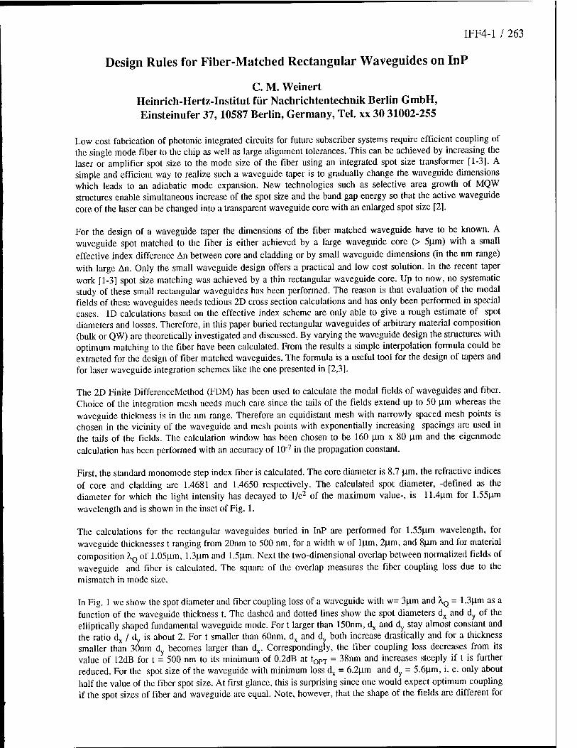
IFF4-1 / 263
Design Rules for Fiber-Matched Rectangular Waveguides on InP
C. M. Weinert Heinrich-Hertz-Institut für Nachrichtentechnik Berlin GmbH, Einsteinufer 37,10587 Berlin, Germany, Tel. xx 30 31002-255
Low cost fabrication of photonic integrated circuits for future subscriber systems require efficient coupling of the single mode fiber to the chip as well as large alignment tolerances. This can be achieved by increasing the laser or amplifier spot size to the mode size of the fiber using an integrated spot size transformer [1-3]. A simple and efficient way to realize such a waveguide taper is to gradually change the waveguide dimensions which leads to an adiabatic mode expansion. New technologies such as selective area growth of MQW structures enable simultaneous increase of the spot size and the band gap energy so that the active waveguide core of the laser can be changed into a transparent waveguide core with an enlarged spot size [2].
For the design of a waveguide taper the dimensions of the fiber matched waveguide have to be known. A waveguide spot matched to the fiber is either achieved by a large waveguide core (> 5(am) with a small effective index difference An between core and cladding or by small waveguide dimensions (in the nm range) with large An. Only the small waveguide design offers a practical and low cost solution. In the recent taper work [1-3] spot size matching was achieved by a thin rectangular waveguide core. Up to now, no systematic study of these small rectangular waveguides has been performed. The reason is that evaluation of the modal fields of these waveguides needs tedious 2D cross section calculations and has only been performed in special cases. ID calculations based on the effective index scheme are only able to give a rough estimate of spot diameters and losses. Therefore, in this paper buried rectangular waveguides of arbitrary material composition (bulk or QW) are theoretically investigated and discussed. By varying the waveguide design the structures with optimum matching to the fiber have been calculated. From the results a simple interpolation formula could be extracted for the design of fiber matched waveguides. The formula is a useful tool for the design of tapers and for laser waveguide integration schemes like the one presented in [2,3].
The 2D Finite DifferenceMethod (FDM) has been used to calculate the modal fields of waveguides and fiber. Choice of the integration mesh needs much care since the tails of the fields extend up to 50 p.m whereas the waveguide thickness is in the nm range. Therefore an equidistant mesh with narrowly spaced mesh points is chosen in the vicinity of the waveguide and mesh points with exponentially increasing spacings are used in the tails of the fields. The calculation window has been chosen to be 160 \xm x 80 (am and the eigenmode calculation has been performed with an accuracy of 10"7 in the propagation constant.
First, the standard monomode step index fiber is calculated. The core diameter is 8.7 ^m, the refractive indices of core and cladding are 1.4681 and 1.4650 respectively. The calculated spot diameter, -defined as the diameter for which the light intensity has decayed to 1/e2 of the maximum value-, is 11.4iim for 1.55nm wavelength and is shown in the inset of Fig. 1.
The calculations for the rectangular waveguides buried in InP are performed for 1.55|im wavelength, for waveguide thicknesses t ranging from 20nm to 500 nm, for a width w of 1 pirn, 2|0.m, and 8|4.m and for material composition XQ of 1.05^m, 1.3(im and 1.5[xm. Next the two-dimensional overlap between normalized fields of waveguide and fiber is calculated. The square of the overlap measures the fiber coupling loss due to the mismatch in mode size.
In Fig. 1 we show the spot diameter and fiber coupling loss of a waveguide with w= 3iim and A.Q = 1.3|am as a function of the waveguide thickness t. The dashed and dotted lines show the spot diameters dx and dy of the elliptically shaped fundamental waveguide mode. For t larger than 150nm, dx and dy stay almost constant and the ratio dx / (L is about 2. For t smaller than 60nm, dx and dy both increase drastically and for a thickness smaller than 3Önm dy becomes larger than dx. Correspondingly, the fiber coupling loss decreases from its value of 12dB for t = 500 nm to its minimum of 0.2dB at tOPT = 38nm and increases steeply if t is further reduced. For the spot size of the waveguide with minimum loss dx = 6.2|j.m and dy = 5.6|j.m, i. e. only about half the value of the fiber spot size. At first glance, this is surprising since one would expect optimum coupling if the spot sizes of fiber and waveguide are equal. Note, however, that the shape of the fields are different for
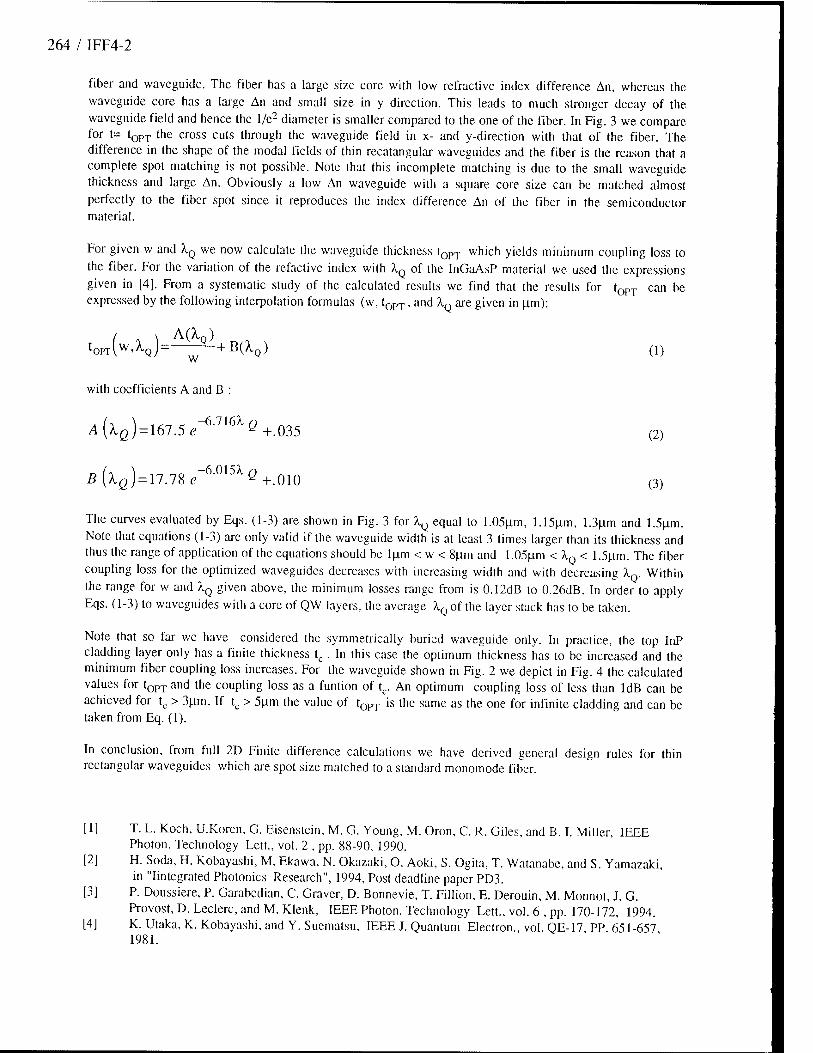
264 / IFF4-2
fiber and waveguide. The fiber has a large size core with low refractive index difference An, whereas the waveguide core has a large An and small size in y direction. This leads to much stronger decay of the waveguide field and hence the 1/e2 diameter is smaller compared to the one of the fiber. In Fig. 3 we compare for t= tOP-j- the cross cuts through the waveguide field in x- and y-direction with that of the fiber. The difference in the shape of the modal fields of thin recatangular waveguides and the fiber is the reason that a complete spot matching is not possible. Note that this incomplete matching is due to the small waveguide thickness and large An. Obviously a low An waveguide with a square core size can be matched almost perfectly to the fiber spot since it reproduces the index difference An of the fiber in the semiconductor material.
For given w and XQ we now calculate the waveguide thickness t0PT which yields minimum coupling loss to the fiber. For the variation of the refactive index with XQ of the InGaAsP material we used the expressions given in [4]. From a systematic study of the calculated results we find that the results for tOPT can be expressed by the following interpolation formulas (w, tOPT, and XQ are given in |am):
A(l0) toPr(w^Q)= ~+B(XQ) (1)
with coefficients A and B :
/l(^ß) = 167.5,-6-7iaß+.035 (2)
5(lö) = 17.78,-6-°mÖ+.010 (3)
The curves evaluated by Eqs. (1-3) are shown in Fig. 3 for XQ equal to 1.05|am, 1.15|am, 1.3pn and 1.5|im. Note that equations (1-3) are only valid if the waveguide width is at least 3 times larger than its thickness and thus the range of application of the equations should be l^m < w < 8(im and 1.05|im < XQ < l.5[im. The fiber coupling loss for the optimized waveguides decreases with increasing width and with decreasing XQ. Within the range for w and ^Q given above, the minimum losses range from is 0.12dB to 0.26dB. In order to apply Eqs. (1-3) to waveguides with a core of QW layers, the average XQ of the layer stack has to be taken.
Note that so far we have considered the symmetrically buried waveguide only. In practice, the top InP cladding layer only has a finite thickness tc . In this case the optimum thickness has to be increased and the minimum fiber coupling loss increases. For the waveguide shown in Fig. 2 we depict in Fig. 4 the calculated values for tOPT and the coupling loss as a funtion of tc. An optimum coupling loss of less than ldB can be achieved for tc > 3(im. If tc > 5|im the value of tOPT is the same as the one for infinite cladding and can be taken from Eq. (1).
In conclusion, from full 2D Finite difference calculations we have derived general design rules for thin rectangular waveguides which are spot size matched to a standard monomode fiber.
[1] T. L. Koch, U.Koren, G. Eisenstein, M. G. Young, M. Oron, C. R. Giles, and B. I. Miller, IEEE Photon. Technology Lett., vol. 2 , pp. 88-90, 1990.
[2] H. Soda, H. Kobayashi, M. Ekawa, N. Okazaki, O. Aoki, S. Ogita, T. Watanabe, and S. Yamazaki, in "Iintegrated Photonics Research", 1994, Post deadline paper PD3.
[3] P. Doussiere, P. Garabedian, C. Graver, D. Bonnevie, T. Fillion, E. Derouin, M. Monnot, J. G. Provost, D. Leclerc, and M. Klenk, IEEE Photon. Technology Lett., vol. 6 , pp. 170-172, 1994.
[4] K. Utaka, K. Kobayashi, and Y. Suematsu, IEEE J. Quantum Electron., vol. QE-17, PP 651-657 1981.
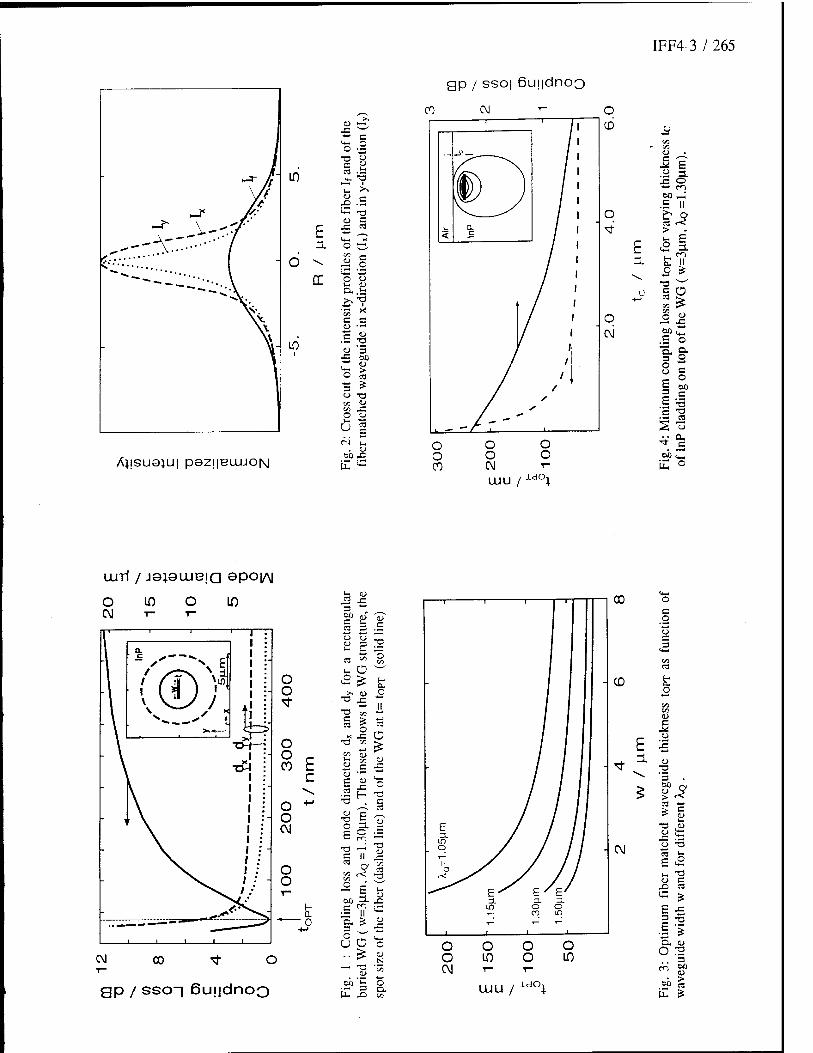
IFF4-3 / 265
10
£
in
ÄJ!SU0}U| pazjiBLUJON
o T3 C U3
C O
•a
T3 c
- O ^ ü CC 8
c o
■o 4)
o u
ob . E !
00
> CTS
<L> x: o
gp / sso| ßujidnoo
CO CM —p. 1 1
- <
Q_ c
. 1 / / / 1 ' 1
/
/ •
CD
O
o CVJ
5 E j= O «-• m oo rt" .£ II
> - <- E
S£
00 d a ° "S. o« 3 P
u
O O CO
O O o o CM i-
UIU / Xd°l
o e o
£ oo
tL,
LUTJ / jaiaujBia ©po|/\|
O U) O Iß CM T- T-
* S
1 1 1 ■ r 1 l :
-1 a. ■ v—\ i l :
1 "
-1 •:®r A' :
- \ \ / X u
- \ K, ■
•O-l :
1 \ 1 : \ • :' \ 1 : \ 1 •■ \ 1 •■ -
X ' : \ 1 •" ^^ ' •"
: _^2^ i i i i i
CM 00 <tf O T-
gp / sso-| ßuüdnoQ
3 *" op o
c ea 3
<L> 3 T3 i- d
C3 M O
v- Ü w
o £ ^ IT u >i qj o ^ . -o x: II
"O t«
« XT a o o CO E
c
iam
eter
s d
The
inse
t s
Xj
o ^v T3
o 4-" "a § o CM £ ° c
' T3 —' •a C II r
o o 8 ^ O -T
V5 03
3 T- — E t-
oo i X)
t - 0
<*- O X
(3 a 141 o
• ■£ 4>
v:
oo = O •— 3 tu X) C/3
c o o c
o
E £ •a '3 oo s r^
LUU / xd°;
Ui
1) äs
w is
I- T3 I) C
X> es «= ^ E £
I? ex tu o :2 . . 3
op ^ E 5:

266 / IFF5-1
Perturbation Model for Computing Optical-Fiber Birefringence from a 2-D Refractive Index Profile
Dipakbin Q. Chowdhury SP-DV-02-4, Corning Inc., Corning, NY 14831 Phone: (607) 974-3593, Fax: (607) 974-3675
and
Daniel A. Nolan SP-FR-01-7, Corning Inc., Corning, NY 14831 Phone: (607) 222-3309, Fax: (607) 974-3675
1 Introduction
In a cylindrically symmetric optical fiber the vector modes are twofold degenerate. Two orthogo-
nally polarized modes have the same propagation constant. Any deviation from perfect azimuthal symmetry would remove the polarization degeneracy, introducing birefringence. For a weakly- guiding fiber scalar perturbation theory have been used successfully to investigate birefringence caused by an elliptic deformation [1-4]. A vector correction to the scalar modes, i.e., a second order perturbation theory, is necessary to compute the birefringence. For an arbitrary 2-D profile these computations are complicated. However, if we start with the vector modes of a radially varying but azimuthally symmetric fiber and then treat the azimuthal variation as a perturbation to the vector modes, only first order perturbation suffice. Here we present a perturbation model based on the above idea. We closely follow the derivation of Ref. [4]. The formulation is applicable to planar waveguides once the vector modes are known.
2 Theory
With the assumption that the waveguide is axially (z-axis) uniform, the transverse vector field components are given by the equation [4],
(V2T + k2n2
re - ß2)ET = -VT( ET • VTlnn2e), (1)
where the free-space propagation constant k = u<J(i0e0, w is the angular frequency, nTt9 is the 2-D refractive index of the medium, and the subscript T denotes transverse components. The temporal and the axial variations are given by exp[z'(u>i - ßz)], where ß is the propagation constant. We rewrite the 2-D index profile as:
nrtg = nT[l + 6frie], n2e w n2
T[l + 28fTß), (2)
where nr is the angle-aver aged-radial variation of the refractive index and the perturbation param- eter 8 <C 1- With the use of Eq. 2 in Eq. 1 we obtain:
(V* + k2n2r - ß2)ET = -VT(ET • VTlnnr
2) - 2Sfc2n2/r,flET - VT[ET • VTln(l + 28fTt$)]. (3)
Since 6frfi < 1, expanding ln(l + 28fTi6) in Taylor series and keeping only terms of 0(8), form Eq. 3 we obtain:
(V2 + k2n2r - ß2)ET = -VT(ET • VT lnnr
2) - 28 [fc2nr2/r,eET + VT(ET • VT/T,9)] . (4)

IFF5-2 / 267
The unperturbed field, eT, is the solution of the equation:
(VJ + k2n2r - ßl)eT + VT(eT • VT lnnr
2) = 0, (5)
where ß0 is the propagation constant of the unperturbed solution. We treat the term in the square bracket in Eq. 4 as a perturbation to Eq. 5 and compute a first order perturbation approximation
for the ß's of the two orthogonally polarized eigenmodes. In the scalar wave approximation the gradient term of Eq. 5 is neglected which introduces an
error of 2-3% in ß0 [5]. Since we are interested in computing changes in ß which are of similar order using only first order perturbation theory, we solve Eq. 5 to compute the vector modes for an azimuthally symmetric fiber. Computation of the vector modes reduces the ß degeneracy of the
modal solution from 4 for the scalar modes to 2. We assume that the perturbed vector field is a linear combination of the two degenerate modes,
i.e.,
ET = Yl X0eTJ (6)
where N is 2 for vector modes and Xj 's are arbitrary coefficients to be determined. The modes are
normalized so that eTi-e*Tjdv = 6i:j, (7)
where 6tj is the Kronecker delta function. From Eqs. 4—7, we obtain:
|y[e^-{Eq.4}-ET-{Eq. 5}*] <fc.
=> If (ej,, • V2TET - ET ■ V2
Te*Ti) ds - {ß2 - ß20)x{ = - ]T Xj ^28 JJ e*Ti ■ k2n2
rfri9eTj ds
+25jJe*Ti ■ VT(eTj • VTfriß)ds + JJ[{e*Ti ■ VT(eTj • VTlnnr2) - {eTj ■ WT{e*Ti ■ VTlnn2)]dS|.
(8) The first integral on the left hand side is a total divergence and the surface integral is converted to a line integral. The line integral is zero since the contour of the integral can be arbitrarily far from the core. The same is true for the last integral on the right hand side. The final form of Eq. 8 is:
{ß2 - ßl)xi = £ XjDij, where A; = -26 JJe*Ti ■ [k2n2fT,eeTj + VT(eTj • VT/r,e)] da, (9) i
where (£, j = 1,2). By computing the eigen values of the matrix D we can calculate the perturbation
(ß2 — ß2) for each mode.
3 Results
To compute the vector solution of Eq. 5 we use the computational method described in Ref. 6. The
electric fields are
ET = ier{r) cos(m6 + ipn), Eg = iee(r) sin(m0 + V«), E, = ez(r) cos(m6 + ipn), (10)
where a temporal and an axial variation of exp[i(wt — ßz)] is implicit and i = \/^l. The two orthogonally polarized modes are found by setting tpn equal to 0 and TT/2 respectively. We compute birefringence due to perturbation of the HEU mode only, i.e., m = 1 in Eq. 10.

268 / IFF5-3
Figure l.a shows the refractive index profile of a fiber. Transverse fields corresponding to Fig. l.a are shown in Fig. l.b. For the perturbation computation we chose an elliptic deformation of the profile where the ellipticity is given as e2 = (1 - r2
min / r2max). For such a deformation,
fr,e = {n(r',6)/nT - l)/6 where n(r,8) is the 2-D refractive index, r' = r[l + G{r) e2 cos2 9]. For an uniform elliptic deformation G(r) = 1. By choosing a suitable G(r) the deformation could be applied around any arbitrary radius. Figure 2 shows computed birefringence Ar in ps/km as a function of wavelength for the profile shown in Fig. l.a. With the assumption of no chromatic dispersion Ar = 6ß/ck„ where Sß « (ß\ - ß\)j2ß0
1.456 -
c is the free space velocity of light.
1.2
4 8 12
Figure 1: In (a) a theoretical refractive index profile for an optical fiber is shown. In (b) fields for the HExi mode, computed from Eq. 5, are shown.
4 Conclusion
1.5
A (fim)
Figure 2: Computed birefringence in ps/km as a function of wavelength is shown. AT = 6ß/ck0
is used to compute the birefringence. Chromatic dispersion is assumed to be zero.
A first order vector perturbation theory is used to compute modal birefringence in optical fibers for an arbitrary 2-D refractive index profile. The perturbation method derived here does not need any field correction and is applicable to various planar waveguide geometries. As an example, birefringence caused by an elliptic perturbation of the HEn mode in an optical fiber is computed as a function of the wavelength. Measured 2-D index profile can be used to compute fiber birefringence which is related to polarization mode dispersion of long lengths of fiber. Such a computation would provide good estimates of correlation length of mode coupling perturbations in a fiber.
References
[1] D. L. A. Tjaden, Phillips J. Res. 33, 254-263 (1978).
[2] M. J. Adams, D. N. Payne, and C. M. Ragdale, Electron. Lett. 15, 298-299 (1979).
[3] R. A. Sammut, C. D. Hussey, J. D. Love, and A. W. Snyder, IEE Proc. 128, 173-187 (1981).
[4] C. Vassallo, Optical Waveguide Concepts (Elsevier, Amsterdam 1991).
[5] H. Ikuno, IEE Proc. J-137, 163-170 (1990).
[6] J. G. Dil and H. Blok, Opto-electronics 5, 415-428 (1973).
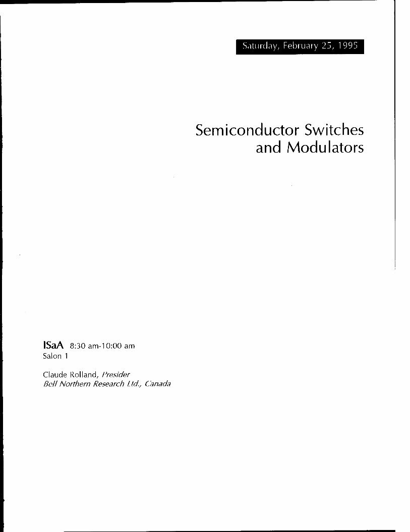
Saturday, February 25, 1995
Semiconductor Switches and Modulators
ISaA 8:30 am-10:00 am Salon 1
Claude Rolland, Presider Bell Northern Research Ltd., Canada

270 / ISaAl-1
An integrated WDM soliton source using sinusoidally driven electroabsorption modulators in a 16 x 1 laser/modulator array
G. Raybon, M. G. Young, U. Koren, B. I. Miller, M. Chien, M. Zirngibl, C. Dragone, N. M. Froberg, and C. A. Burrus
AT&T Bell Laboratories, Crawford Hill Laboratory
791 Holmdel-Keyport Rd, Holmdel, NJ 07733, U.S.A. (908)888-7221
Trans-oceanic soliton transmission systems employing optical amplifiers and 'sliding-frequency guiding filters' have the potential to reach capacities of 100 Gbit/s through extensive wavelength division multiplexing [1]. The sliding-frequency filter transmission line lends itself to wavelength multiplexing because of the periodic nature of the Fabry Perot filter. Each wavelength can be guided along the transmission fiber without interactions with neighboring solitons, excessive timing jitter or noise accumulation. However, practical application of soliton systems has been slowed by lack of a reliable pulse source. Recently, soliton transmission using a sinusoidally driven electroabsorption modulated laser as the pulse source has been demonstrated [2]. The integrated DFB or DBR laser/modulator offers great potential as a soliton source because it is compact, manufacturable, and offers flexible operation in terms of repetition rate, pulse width and wavelength. Here we report the pulsed operation of a WDM photonic integrated circuit (PIC) consisting of 16 DBR lasers, 16 electroabsorption modulators, a passive optical combiner and an optical amplifier [3]. Previously, multi-wavelength low chirp NRZ transmission using the 16 x 1 PIC at 1.7 Gbit/s had been reported [4]. Here the device is functioning as a four channel pulse generator operating at 2.5 GHz producing near transform limited pulses with an average width of 63 ps.
The 16x1 PIC transmitter, shown in Fig. 1, consists of 16 tunable distributed Bragg reflector (DBR) lasers and 16 electroabsorption (EA) modulators. The gratings of each DBR laser are varied using stepped holographic exposures to obtain lasing wavelengths over a range of 1.545 ^m to 1.555 \im and an average channel spacing of 6.7 A. Each laser output is guided in a buried rib passive waveguide and all are combined in a passive free space radiation region. The combined signals are amplified in a 650 urn long multiple quantum well (MQW) optical amplifier followed by a window region. The 4 mm by 6 mm chip is mounted in a package which provides optical coupling to single mode fiber via a micromachined lensed fiber and electrical access to the potential 53 contacts. In the present package, 30 connections are made, including eight which are high speed contacts to the EA modulators, and one connection which allows tuning of the lasing wavelength of
Synthesizer
Synthesizer
IASB? MOOULATOR AMPUflB? PACKAGED
'16 x 1 LASER/MODULATOR ARRAY Streak
Camera
Fabry Perot Interferometer
Fig. 1: Experimental set-up for characterizing WDM pulse output from a 16 x 1 laser/modulator array.
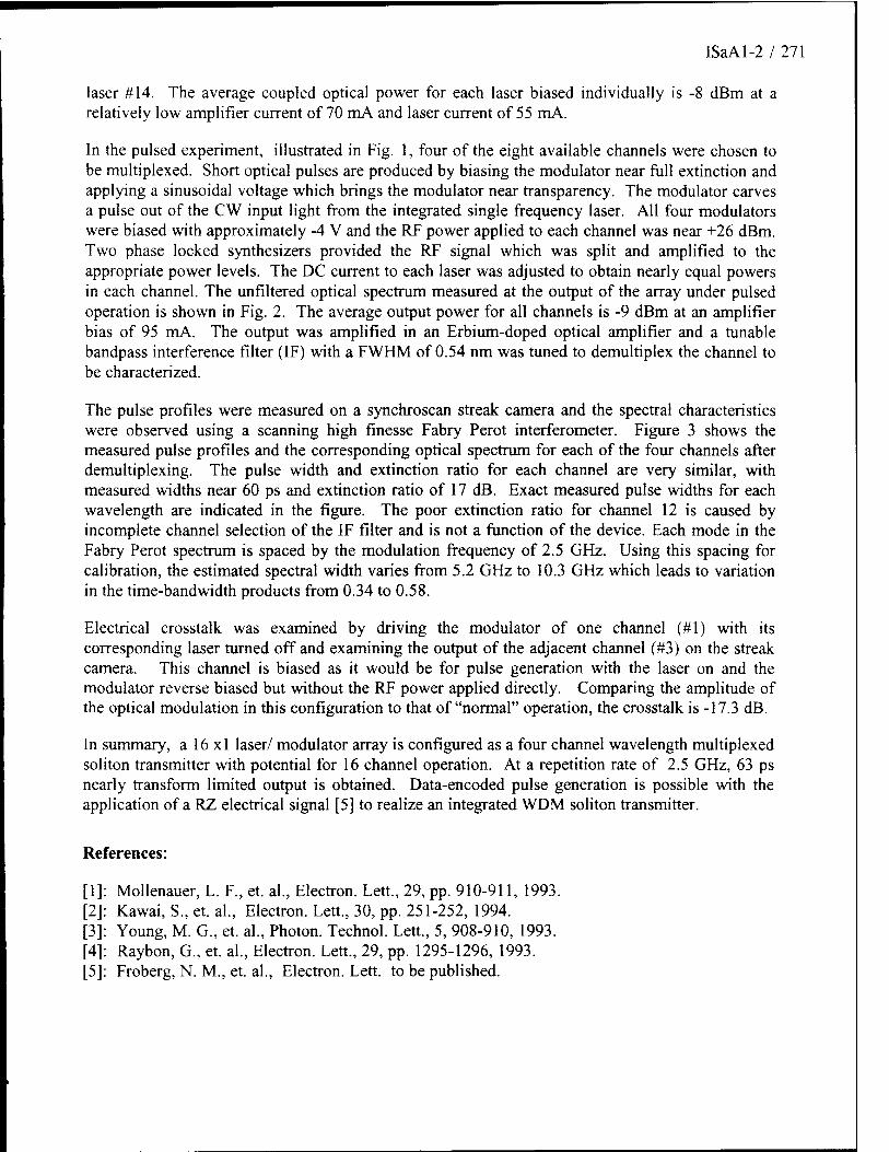
ISaAl-2 / 271
laser #14. The average coupled optical power for each laser biased individually is -8 dBm at a relatively low amplifier current of 70 mA and laser current of 55 mA.
In the pulsed experiment, illustrated in Fig. 1, four of the eight available channels were chosen to be multiplexed. Short optical pulses are produced by biasing the modulator near full extinction and applying a sinusoidal voltage which brings the modulator near transparency. The modulator carves a pulse out of the CW input light from the integrated single frequency laser. All four modulators were biased with approximately -4 V and the RF power applied to each channel was near +26 dBm. Two phase locked synthesizers provided the RF signal which was split and amplified to the appropriate power levels. The DC current to each laser was adjusted to obtain nearly equal powers in each channel. The unfiltered optical spectrum measured at the output of the array under pulsed operation is shown in Fig. 2. The average output power for all channels is -9 dBm at an amplifier bias of 95 mA. The output was amplified in an Erbium-doped optical amplifier and a tunable bandpass interference filter (IF) with a FWHM of 0.54 nm was tuned to demultiplex the channel to be characterized.
The pulse profiles were measured on a synchroscan streak camera and the spectral characteristics were observed using a scanning high finesse Fabry Perot interferometer. Figure 3 shows the measured pulse profiles and the corresponding optical spectrum for each of the four channels after demultiplexing. The pulse width and extinction ratio for each channel are very similar, with measured widths near 60 ps and extinction ratio of 17 dB. Exact measured pulse widths for each wavelength are indicated in the figure. The poor extinction ratio for channel 12 is caused by incomplete channel selection of the IF filter and is not a function of the device. Each mode in the Fabry Perot spectrum is spaced by the modulation frequency of 2.5 GHz. Using this spacing for calibration, the estimated spectral width varies from 5.2 GHz to 10.3 GHz which leads to variation in the time-bandwidth products from 0.34 to 0.58.
Electrical crosstalk was examined by driving the modulator of one channel (#1) with its corresponding laser turned off and examining the output of the adjacent channel (#3) on the streak camera. This channel is biased as it would be for pulse generation with the laser on and the modulator reverse biased but without the RF power applied directly. Comparing the amplitude of the optical modulation in this configuration to that of "normal" operation, the crosstalk is -17.3 dB.
In summary, a 16 xl laser/ modulator array is configured as a four channel wavelength multiplexed soliton transmitter with potential for 16 channel operation. At a repetition rate of 2.5 GHz, 63 ps nearly transform limited output is obtained. Data-encoded pulse generation is possible with the application of a RZ electrical signal [5] to realize an integrated WDM soliton transmitter.
References:
[1] [2] [3] [4] [5]
Mollenauer, L. F., et. al., Electron. Lett., 29, pp. 910-911, 1993. Kawai, S., et. al., Electron. Lett., 30, pp. 251-252, 1994. Young, M. G., et. al., Photon. Technol. Lett., 5, 908-910, 1993. Raybon, G., et. al, Electron. Lett., 29, pp. 1295-1296, 1993. Froberg, N. M., et. al., Electron. Lett, to be published.

272 / ISaAl-3
-10
CD "Ö
1-30
-50
#10: :#3. : #1: "'
;#12; j I ': [ :
u 1.547 1.552
Wavelength, |im 1.557
Fig. 2: Optical spectrum of four channels at the output of the 16 x array under pulsed operation.
3.5 GHz
5.2 GHz,
■ i ... i.... i.
E5.3 GHz,
. i. . i.,,, i,, i i,
." " i" " i" ■' i' :1 0.3 GHz
i ... i,,., i. . i..
Optical Frequency
(2.5 GHz/mode)
Fig.3: Streak camera recordings of pulse streams and corresponding optical spectrum of four demultiplexed wavelengths. Pulse width and spectral width indicated within each figure.

ISaA2-l / 273
High-Speed Operation of Quantum Well Electron Transfer Digital Optical Switches
M. N. Khan, J. E. Zucker, T. Y. Chang, N. J. Sauer, C. A. Burrus and G. Raybon AT&T Bell Laboratories Crawfords Corner Road
Rm4F-311 Holmdel, NJ 07733
Tel: (908) 949-9135 Fax: (908) 949-8988
Optical time division multiplexing (OTDM) is a powerful means of increasing optical network capacity while still employing relatively inexpensive low-speed electronics. The critical and limiting component in such systems is the demultiplexer that picks apart the high-data-rate optical bit stream before detection and electrical signal processing at a lower data rate. Electro- optic demultiplexing using high-speed lithium niobate waveguide devices, either 1X2 switches or on/off modulators , has thus far been the most successful method for OTDM system demonstrations, although recently semiconductor modulators have also been used. Semiconductor 1X2 switches are attractive for this application since they simultaneously perform both the gating and routing function, can be easily monolithically integrated with detectors, and monolithically cascaded to form a binary tree array . Optical network system requirements for switches include low crosstalk, polarization-independence, and a wide operating range of wavelengths. Also in keeping with the desire for low-cost, off-the-shelf electronics, low drive voltage is extremely important. These features have recently been demonstrated in semiconductor digital 1X2 switches based on InGaAs/InGaAlAs Barrier, Reservoir, and Quantum Well Electron Tranfer (BRAQWET) structures . However these switches have only been tested at DC.
In this paper, we demonstrate the first high-speed operation of a BRAQWET digital switch. By using compact switches with low-dielectric-constant planarization, we minimize the capacitance of the device, resulting in an RC-limited electrical bandwidth of 5 GHz. Fig. 1 shows a schematic of the y-branch, which is shaped with two angles to provide weighted coupling between the two branches. This shape results in enhanced crosstalk performance, -19 dB into lensed fiber, with a low voltage-length product for switching, 4 V-mm .
ion implant Au pad
lnGaAs:Si
polyimide InGaAs/lnGaAIAs quantum wells
Fig.l. High-speed shaped Y- branch switch with active length 1.2 mm. Opening angle is 0.5° and final angle between output ports is 0.2°. Contact pads (only one is shown for clarity) are 200 X 55 pm2. Upper and lower InGaAs:Si cladding layers enclose the 0.8028 pm thick electro- optically active core comprised of 12 chopped BRAQWET periods. Rib etch depth and width are d= 1.4 pm and w=2.5 pm.
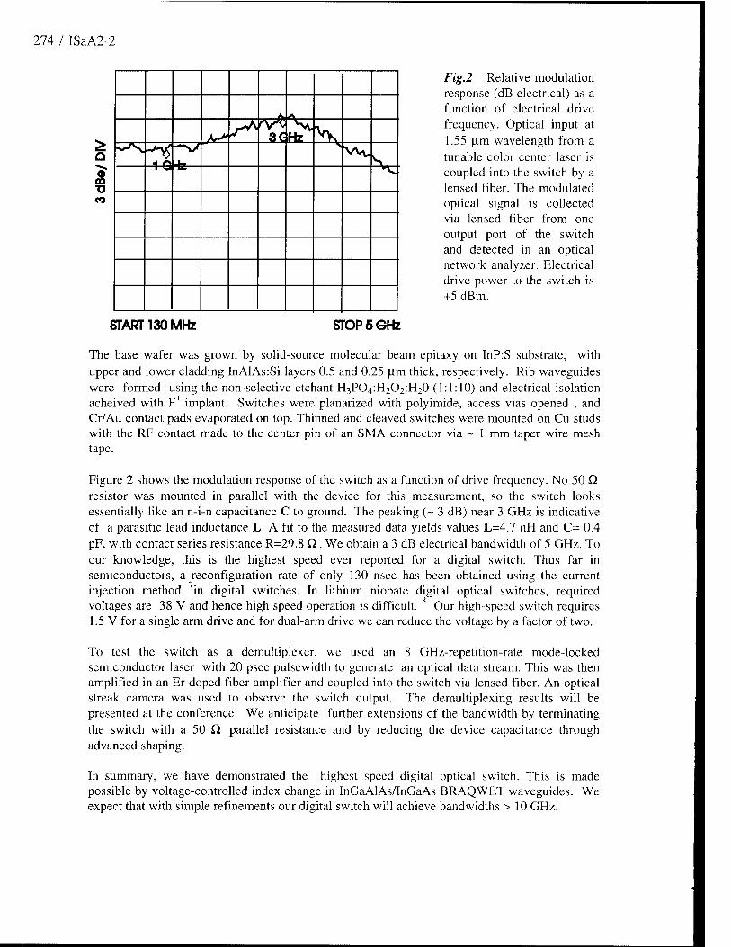
274 / ISaA2-2
/s A
hr* s* 3C Hz X a A nitm
\ Vvv V vv.
CO
Fig.2 Relative modulation response (dB electrical) as a function of electrical drive frequency. Optical input at 1.55 \x.m wavelength from a tunable color center laser is coupled into the switch by a lensed fiber. The modulated optical signal is collected via lensed fiber from one output port of the switch and detected in an optical network analyzer. Electrical drive power to the switch is +5 dBm.
START 130 MHz STOP 5 GHz
The base wafer was grown by solid-source molecular beam epitaxy on InP:S substrate, with upper and lower cladding InAlAs:Si layers 0.5 and 0.25 um thick, respectively. Rib waveguides were formed using the non-selective etchant H3PO4:H2O2:H20 (1:1:10) and electrical isolation acheived with F implant. Switches were planarized with polyimide, access vias opened , and Cr/Au contact pads evaporated on top. Thinned and cleaved switches were mounted on Cu studs with the RF contact made to the center pin of an SMA connector via ~ 1 mm taper wire mesh tape.
Figure 2 shows the modulation response of the switch as a function of drive frequency. No 50 Q. resistor was mounted in parallel with the device for this measurement, so the switch looks essentially like an n-i-n capacitance C to ground. The peaking (~ 3 dB) near 3 GHz is indicative of a parasitic lead inductance L. A fit to the measured data yields values L=4.7 nH and C= 0.4 pF, with contact series resistance R=29.8 Q. We obtain a 3 dB electrical bandwidth of 5 GHz. To our knowledge, this is the highest speed ever reported for a digital switch. Thus far in semiconductors, a reconfiguration rate of only 130 nsec has been obtained using the current injection method in digital switches. In lithium niobate digital optical switches, required voltages are 38 V and hence high speed operation is difficult. Our high-speed switch requires 1.5 V for a single arm drive and for dual-arm drive we can reduce the voltage by a factor of two.
To test the switch as a demultiplexer, we used an 8 GHz-repetition-rate mode-locked semiconductor laser with 20 psec pulsewidth to generate an optical data stream. This was then amplified in an Er-doped fiber amplifier and coupled into the switch via lensed fiber. An optical streak camera was used to observe the switch output. The demultiplexing results will be presented at the conference. We anticipate further extensions of the bandwidth by terminating the switch with a 50 ß parallel resistance and by reducing the device capacitance through advanced shaping.
In summary, we have demonstrated the highest speed digital optical switch. This is made possible by voltage-controlled index change in InGaAlAs/InGaAs BRAQWET waveguides. We expect that with simple refinements our digital switch will achieve bandwidths > 10 GHz.
ISaA2-3 / 275
REFERENCES
1 "Optical Time-Division Multiplexing for Very High Bit-Rate Transmission," R. S. Tucker, G. Eisenstein, S. K. Korotky, J. Lightwave Technol. 6, 1737 (1988). 2 "Ultrafast time-division demultiplexer based on electrooptic on-off gates," M. Jinno, J. Lightwave Technol. 10, 1458(1992). 3 "Three-node, 40 Gbit/s OTDM network experiment using electro-optic switches," A. D. Ellis, T. Widdowson, X. Shan and D. G. Moodie, Electron. Lett. 30, 1333 (1994). 4 "Ultrafast photonic ATM switch with optical output buffers," Y. Shimazu and M. Tsukada, J. Lightwave Technol. 10, 265 (1992). 5"Weighted coupling y branch optical switch in InGaAs/InGaAlAs quantum well electron transfer waveguides," M. N. Khan, J. E. Zucker, T. Y. Chang, N. J. Sauer and M. D. Divino, Photon. Technol. Lett. 3, 394 (1994). 6 "Design and demonstration of weighted coupling digital y-branch optical switches in InGaAs/InGaAlAs electron transfer waveguides," M. N. Khan, J. E. Zucker, T. Y. Chang, N. J. Sauer, M. D. Divino, T. L. Koch, C. A. Burrus and H. M. Presby, J. Lightwave Technol. 12 (November 1994). 7 "The InP digital optical switch: a key element for guided wave photonic switching,"! F. Vinchant, M. Renaud, M. Erman, J. L. Peyre, P. Jarry and P. Pagnod-Rossiaux, IEE Proceedings-J. vol. 140, no. 5, pp. 301-307, October 1993. 8 "An 8X8 Ti:LiNb03 Polarization-Independent Photonic Switch," T.O. Murphy, E. J. Murphy, and R. W. Irvin, ECOC'94 Proceedings, vol.2, pp. 549-552.

276 / ISaA3-l
High-speed modulation and short pulse generation using
MQW modulators with integrated light sources
Koichi Wakita
NTT Opto-electronics Laboratories
3-1, Morinosato Wakamiya, Atsugi-Shi, Kanagawa, 243-01, Japan
Tel. (81)462-40-2821 Fax.(81)462-40-4383
Introduction: MQW electroabsorption (EA) modulators have been
studied since they were first reported by AT&T group [T], and low
driving voltage (<2 V) and large 3-dB bandwidth (>20 GHz) have
been achieved for InGaAs/InAlAs [2] and InGaAsP/InGaAsP [3]
MQWs operating at long wavelengths. 20-Gbit/s transmission over
100-km using a monolithically integrated light source module
consisting of an MQW modulator and a DFB laser has also been
reported [4J.
Discrete Devices: The bandwidth-to-drive-voltage ratio versus
detuning energy is an important figure of merit for external
modulators [4]. Figure 1 shows this figure of merit for reported
semiconductor modulators, and shows that a thick quantum well
results in a large figure of merit. In this figure propagation loss is
not considered. Figure 2 shows absorption plotted against the
product of sample length and the operating voltage required to obtain an on/off ratio of 10-dB or a phase shift of K. It is remark-
able that for any external modulator there is a trade-off between
the product and propagation loss. That is, MQW structures have
little propagation loss because they are short, but their loss per unit
length is high.
The hole barrier height has a detrimental effect on the frequen-
cy response when the input optical power is high, and an InGaAsP
/InP MQW has handicaps because of its large valence band offset.
Using an InGaAsP/InGaAsP structure reduces the band offset and
results in high power saturation [6], while also resulting in weak
quantum confinement and large field-induced broadening [7].
Compressive strain in the well increases the optical power satura-
tion [8], whereas polarization insensitivity is obtained by intro-
ducing tensile strain [9]. Figure 3 shows that the polarization sen-
sitivity is less than 1 dB for InGaAs/InAlAs MQWs with extinction
ratio over 30 dB. The figure of merit for this kind of device is
higher than that for unstrained modulators.

ISaA3-2 / 277
Pulse generation and coding: A MQW EA modulator provides optical
pulses with a small duty ratio because its absorption coefficient changes markedly in response to applied voltage [10]. The repeti- tion rate is limited only by the frequency response of the modula- tor. 10-Gbit/s optical soliton transmission over 7200 km and with a bit-error-rate lower than 10"9 has been demonstrated by using a monolithically integrated light source [11], and short-pulse genera- tion and coding [12] have been produced by using a multisection MQW modulator monolithically integrated with a DFB laser. Figure 4 is a schematic diagram of this new device. While pulses are gener- ated by one modulator, the other modulator is driven with a 10-G bit/s NRZ signal synchronized with the sinusoidal RF wave. Figure 5 shows the eye-pattern observed with a photo- detector. The data are encoded at 10-Gbit/s and the pulse full-width-at-half-maxi- mum is 17 psec. The high coupling loss can thus be overcome by integrating the modulators and light source.
Active mode locking by monolithic integrated EA modulators is also efficient [13]. The modulator acts as a short optical pulse gate when a sinusoidal voltage is driven at a deep bias point. As shown in Fig. 6, an optical pulse width of 2 psec was obtained at 16.3 GHz by a 2.5-mm-long laser monolithically integrated with an MQW modulator.
MQW modulators and their monolithically integrated light sources can be expected to be used in all optical transmission systems as well as in interconnect and signal processing systems because of their low power consumption and high-speed operation. References: [I] D. S. Chemla et al., Appl. Phys. Lett., 42, 864, 1983. [2] T. Ido et al., OEC'94, 15B3-1, 1994. [3] F. Devaux et al., Photon. Technol. Lett., 5, 1288, 1993. [4] T. Kataoka et al., Elecron. Lett., 30, 872, 1994. [5] K. Wakita and I. Kotaka, Micro. Opt. Technol. Lett., 7, 120, 1994. [6] M. Aoki et al., Electron. Lett., 28, 1157, 1992. [7] T, Yamanaka et al., Appl. Phys. Lett., 65, 1540, 1994. [8] I. K. Czajkowski et al., Electron. Lett., 30, 900, 1994. [9} J. E. Zucker et al., IPR'92, Pd7, 1992. [10] K. Wakita et al., Electron. Lett., 29, 718, 1993. [II] S. Kawai et al., Electron. Lett., 30, 251, 1994. [12] K. Sato et al., Electron. Lett., 30, 1144, 1994. [13] K. Sato et al., Appl. Phys. Lett., 65, 1, 1994.

278 / ISaA3-3
E
N
a ,5
o
a) 3 CD
on/olf ralio:20dB '
InGaAs/lnAlAs MQW(67/67! InGaAsP/lnGaAsP
MQWCI00/50)
\1
InGaAs/lnGaAsP
MQW(50/80)
InGaAsP/lnP x
bulk V^,
InGaAs/lnAIAs MOY/175/50)
\ In Ga Al As/ In Al As
\^ MOW PM
^* EO
GaAs/AJGaÄs
1000
? P3 1 00 ■a
c c
Q. 1_ O t/i
0.1
: Ü ,
a A ■ a
a ■ ■ a
A r o GaAs Homo -f ■
o'« -
: a GaAs MQW A-t- ° A ■ InP MQW + o
X LN : + GaAs Hetero ++ f
A InP Hetero
• InP Homo
,( . ... X
energy difference (meV)
Fig. 1 Figure of mcrii vs. detuning energy. PM and EO indicate phase and electrooptic modulators. Numbers in parentheses are the thickness (Ä) of the well and the barrier.
001 01 1 10 100
product of voltage and sample length (Vcm)
Fig. 2. Absorption vs. the product of operating voltage and sample length.
MQW-LD
CD T3
•20 -
Z -30
c = •40
o J= — -so X ID
. —'•""-■—"""—'I"" • —
1.58TE
5^>r^-v 1.56TE 1.56TM
N \ t V i
I.55TE 1.55TM 1 5-1TE
• \ '* \ \ 1 54TM
m ' "■ Y_"~ " "'—^\ — " ~* . _ 1
0 12 3 4 5
reverse voltage (V)
F'g, 3 Extinction ratio vs. applied voltage for a tensile-strained MQW modulator.
time 200 ps
F'«. 2 Optical pulses encoded with a 10-Gbit/s pseudo-random bit signal.
n-lnP
F'g- 4 Monolithically integrated MQW EA modulators and DFB laser.
Fit?. 6 Autocorrelation trace of the pulse train obtained from the mode-locked monolithically integrated light source.
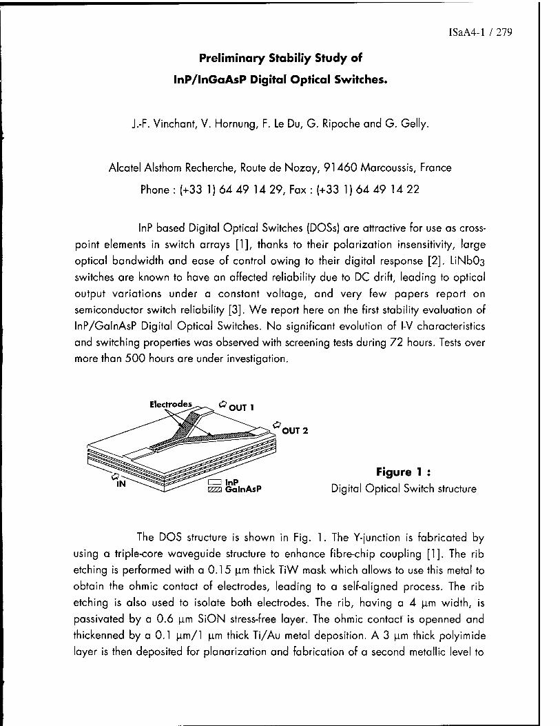
ISaA4-l / 279
Preliminary Stabiliy Study of
InP/lnGaAsP Digital Optical Switches.
J.-F. Vinchant, V. Hornung, F. Le Du, G. Ripoche and G. Gelly.
Alcatel Alsthom Recherche, Route de Nozay, 91460 Marcoussis, France
Phone : (+33 1) 64 49 14 29, Fax : (+33 1) 64 49 14 22
InP based Digital Optical Switches (DOSs) are attractive for use as cross-
point elements in switch arrays [1], thanks to their polarization insensitivity, large
optical bandwidth and ease of control owing to their digital response [2]. LiNbÜ3
switches are known to have an affected reliability due to DC drift, leading to optical
output variations under a constant voltage, and very few papers report on
semiconductor switch reliability [3]. We report here on the first stability evaluation of
InP/GalnAsP Digital Optical Switches. No significant evolution of l-V characteristics
and switching properties was observed with screening tests during 72 hours. Tests over
more than 500 hours are under investigation.
Electrodes^^ ^OUT 1
Figure 1 : r~ | |np
urn GalnAsP Digital Optical Switch structure
The DOS structure is shown in Fig. 1. The Y-junction is fabricated by
using a triple-core waveguide structure to enhance fibre-chip coupling [1]. The rib
etching is performed with a 0.15 |im thick TiW mask which allows to use this metal to
obtain the ohmic contact of electrodes, leading to a self-aligned process. The rib
etching is also used to isolate both electrodes. The rib, having a 4 (im width, is
passivated by a 0.6 |im SiON stress-free layer. The ohmic contact is openned and
thickenned by a 0.1 u.m/1 |im thick Ti/Au metal deposition. A 3 u.m thick polyimide
layer is then deposited for planarization and fabrication of a second metallic level to
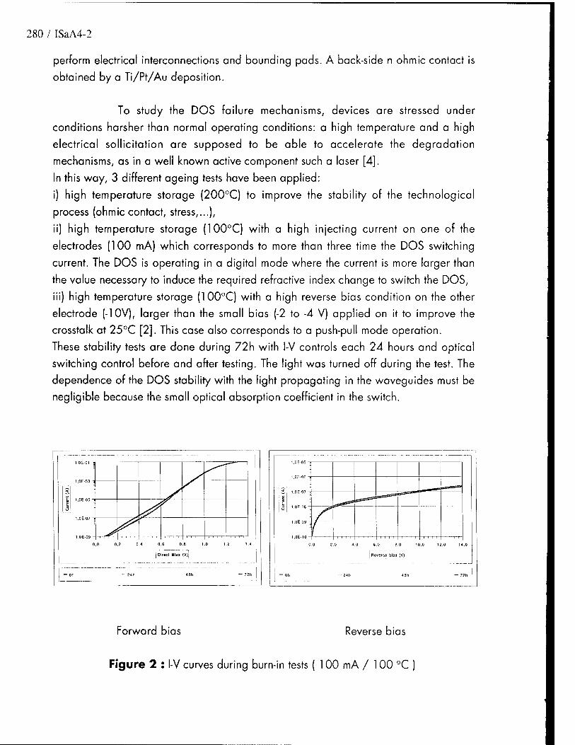
280 / ISaA4-2
perform electrical interconnections and bounding pads. A back-side n ohmic contact is
obtained by a Ti/Pt/Au deposition.
To study the DOS failure mechanisms, devices are stressed under
conditions harsher than normal operating conditions: a high temperature and a high
electrical sollicitation are supposed to be able to accelerate the degradation
mechanisms, as in a well known active component such a laser [4].
In this way, 3 different ageing tests have been applied:
i) high temperature storage (200°C) to improve the stability of the technological
process (ohmic contact, stress,...),
ii) high temperature storage (100°C) with a high injecting current on one of the
electrodes (100 mA) which corresponds to more than three time the DOS switching
current. The DOS is operating in a digital mode where the current is more larger than
the value necessary to induce the required refractive index change to switch the DOS,
iii) high temperature storage (100°C) with a high reverse bias condition on the other
electrode (-10V), larger than the small bias (-2 to -4 V) applied on it to improve the
crosstalk at 25°C [2]. This case also corresponds to a push-pull mode operation.
These stability tests are done during 72h with l-V controls each 24 hours and optical
switching control before and after testing. The light was turned off during the test. The
dependence of the DOS stability with the light propagating in the waveguides must be
negligible because the small optical absorption coefficient in the switch.
—
< t
1.0E-07 -s
1.0E-09 ~
0 0 0 2 0 4 0 6 0 8 1 0 1 2 1 4
j Direct Bias (V)|
— Oh
_. __... 24h 48h — 72h
- - - " !
1.0E-06 i
1 U 1.0E-0S -
1.0E-10 - i i i i 1 ' ' ' i i i i i i r
1 i < i i i i i i
0,0 2 0 4 0 6.0 8,0 10,0 12,0 14,0
Reverse bias (V)
[ " — Oh ' 24h 48h — 72h
Forward bias Reverse bias
Figure 2 : l-V curves during burn-in tests ( 100 mA / 100 °C )

ISaA4-3 / 281
Statistics on DOS l-V curves were done. The switching current is below
30 mA and the voltage required on 200 electrodes to reach 30 mA is 1.2 V
(±0.1 V). 95 % of 2mm long electrodes have a leakage current at -10 V below
100 nA. These results illustrate the high quality of technological process and epitaxial
growth on 2 inch wafers. Forward and reverse l-V curves after 0, 24, 48 and 72 hours
are shown on Fig. 2 after a 100°C temperature storage and simultaneously a 100mA
current on the right arm of the DOS. The small change in the low level of the forward
l(V) curve could be attributed to the profitable temperature effect on the rib technology.
Similar results are obtained in the other screening tests (- 10 V /l 00 °C). The switching
curves of a DOS before and after the current/temperature test are shown in Fig. 3.
The crosstalk values at 20 mA are respectively -12.5 and -13.1 dB, showing no
significant evolution.
1.0
0.8
° 0.6
I f" 0.4 3 a. *. 3 o
0.2 h
0.0
Da°aD„__ . °Q D[
a Before testing * After 100°C/100mA
10 15 20 25
Current, mA
30
Figure 3 : DOS switching curves before and after the screening:
100°C / 100mA on one arm / 72h
For the first time, preliminary studies on the stability of InP based Digital Optical
Switches are reported. No significant evolution is observed. Longer tests (more than
500 hours, 100 °C, 100 mA) are under investigation. These first results are very
promising for InP DOS switch array manufacturing.
1. J.F. Vinchant et al., ECOC93, paper ThC 12.4, Montreux, Switzerland, 1993
2.J.F. Vinchantetal., IEE Proc.-J, 140(5), pp. 301-307, 1993
3. K. Hamamotoetal.JpnJ. Appl. Phys., Pt. 2, n° 3B, pp. 390-391, 1993
4. M. Fukuda, Reliability and degradation of semicond. lasers and LEDs, Artech House, 1991
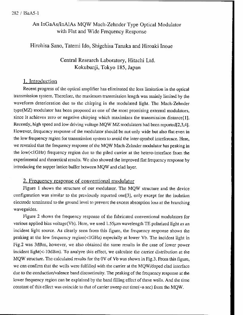
282 / ISaA5-l
An InGaAs/InAlAs MQW Mach-Zehnder Type Optical Modulator with Flat and Wide Frequency Response
Hirohisa Sano, Tatemi Ido, Shigehisa Tanaka and Hiroaki Inoue
Central Research Laboratory, Hitachi Ltd. Kokubunji, Tokyo 185, Japan
1. Introduction Recent progress of the optical amplifier has eliminated the loss limitation in the optical
transmission system. Therefore, the maximum transmission length was mainly limited by the
waveform deterioration due to the chirping in the modulated light. The Mach-Zehnder
type(MZ) modulator has been proposed as one of the most promising external modulators,
since it achieves zero or negative chirping which maximizes the transmission distance[l].
Recently, high speed and low driving voltage MQW MZ modulators had been reported[2,3,4].
However, frequency response of the modulator should be not only wide but also flat even in
the low frequency region for transmission system to avoid the inter-symbol interference. Here,
we revealed that the frequency response of the MQW Mach-Zehnder modulator has peaking in
the low(<lGHz) frequency region due to the piled carrier at the hetero-interface from the
experimental and theoretical results. We also showed the improved flat frequency response by
introducing the supper lattice buffer between MQW and clad layer.
2. Frequency response of conventional modulator Figure 1 shows the structure of our modulator. The MQW structure and the device
configuration was similar to the previously reported one[3], only except for the isolation
electrode terminated to the ground level to prevent the excess absorption loss at the branching
waveguides.
Figure 2 shows the frequency response of the fabricated conventional modulators for
various applied bias voltage(Vb). Here, we used 1.55(im wavelength TE polarized light as an
incident light source. As clearly seen from this figure, the frequency response shows the
peaking at the low frequency region(<lGHz) especially at lower Vb. The incident light in
Fig.2 was 3dBm, however, we also obtained the same results in the case of lower power
incident light(<-10dBm). To analyze this effect, we calculate the carrier distribution at the
MQW structure. The calculated results for the OV of Vb was shown in Fig.3. From this figure,
we can confirm that the wells were fulfilled with the carrier at the MQW/doped clad interface
due to the conduction/valence band discontinuity. The peaking of the frequency response at the
lower frequency region can be explained by the band filling effect of these wells. And the time
constant of this effect was coincide to that of carrier sweep out time(~n sec) from the MQW.
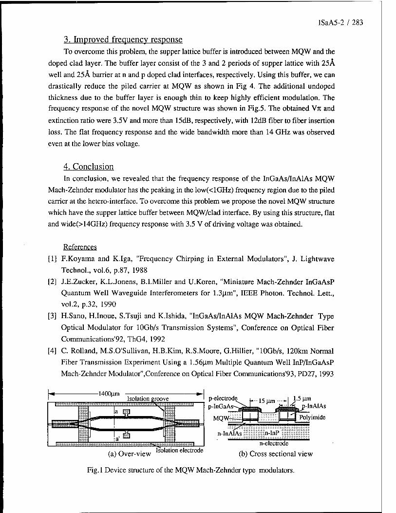
ISaA5-2 / 283
3. Improved frequency response To overcome this problem, the supper lattice buffer is introduced between MQW and the
doped clad layer. The buffer layer consist of the 3 and 2 periods of supper lattice with 25Ä
well and 25Ä barrier at n and p doped clad interfaces, respectively. Using this buffer, we can
drastically reduce the piled carrier at MQW as shown in Fig 4. The additional undoped
thickness due to the buffer layer is enough thin to keep highly efficient modulation. The frequency response of the novel MQW structure was shown in Fig.5. The obtained Wit and
extinction ratio were 3.5V and more than 15dB, respectively, with 12dB fiber to fiber insertion
loss. The flat frequency response and the wide bandwidth more than 14 GHz was observed
even at the lower bias voltage.
4. Conclusion In conclusion, we revealed that the frequency response of the InGaAs/InAlAs MQW
Mach-Zehnder modulator has the peaking in the low(<lGHz) frequency region due to the piled
carrier at the hetero-interface. To overcome this problem we propose the novel MQW structure
which have the supper lattice buffer between MQW/clad interface. By using this structure, flat
and wide(>14GHz) frequency response with 3.5 V of driving voltage was obtained.
References
[1] F.Koyama and K.Iga, "Frequency Chirping in External Modulators", J. Lightwave
Technol., vol.6, p.87, 1988
[2] J.E.Zucker, K.L.Jonens, B.I.Miller and U.Koren, "Miniature Mach-Zehnder InGaAsP
Quantum Well Waveguide Interferometers for 1.3um", IEEE Photon. Technol. Lett.,
vol.2, p.32, 1990
[3] H.Sano, H.Inoue, S.Tsuji and K.Ishida, "InGaAs/InAlAs MQW Mach-Zehnder Type
Optical Modulator for 10Gb/s Transmission Systems", Conference on Optical Fiber
Communications'92, ThG4, 1992
[4] C. Rolland, M.S.O'Sullivan, H.B.Kim, R.S.Moore, G.Hillier, "10Gb/s, 120km Normal
Fiber Transmission Experiment Using a 1.56(im Multiple Quantum Well InP/InGaAsP
Mach-Zehnder Modulator".Conference on Optical Fiber Communications'93, PD27, 1993
p-electrode p-InGaA
MQW—
n-InAlAs
15um-H >5^m
- Iy* -InAlAs
Polyimide
n-InP i
Isolation electrode n-electrode
(b) Cross sectional view (a) Over-view
Fig.l Device structure of the MQW Mach-Zehnder type modulators.

284 / ISaA5-3
2GHz/div
0.13GHz 10GHz 20GHz
Fig.2 Frequency response of MQW MZ modulator (Conventional MQW)
n-InAlAs MQW H^
InAlAs i!8
9 1 *■—'
B o fc -1
— Ef ;;•- WUVVUIAA-—
Electron
..4....;...£...e...g...y...,....?...^...«..-
V'" Distance Fig.3 Calculated results of potential and carrier
distribution (Vb=0V)
:MQW with supper lattice buffer ;...£-...•....;...£...4...«....;....;....)... $., ■ ■ ■ ::::::::
I-I - j... i NÜ l,U.. ii;;iNdoPe-lXlCr7i:S:i
>.-ö —I—*-—-5— c—1—§"*"*i— t'"t"
i i i I ■ ■ ■ i 1 -0.5 -1.0 -1.5 -2.0
Applied voltage (V) Fig.4 Maximum electron density at MQW
2GHz/div
Incident light = 3dBm 1 1 1 ■
ov :
0.13GHz 10GHz 20GHz
Fig.5 Frequency response of MQW MZ modulator (MQW with supper lattice buffer)
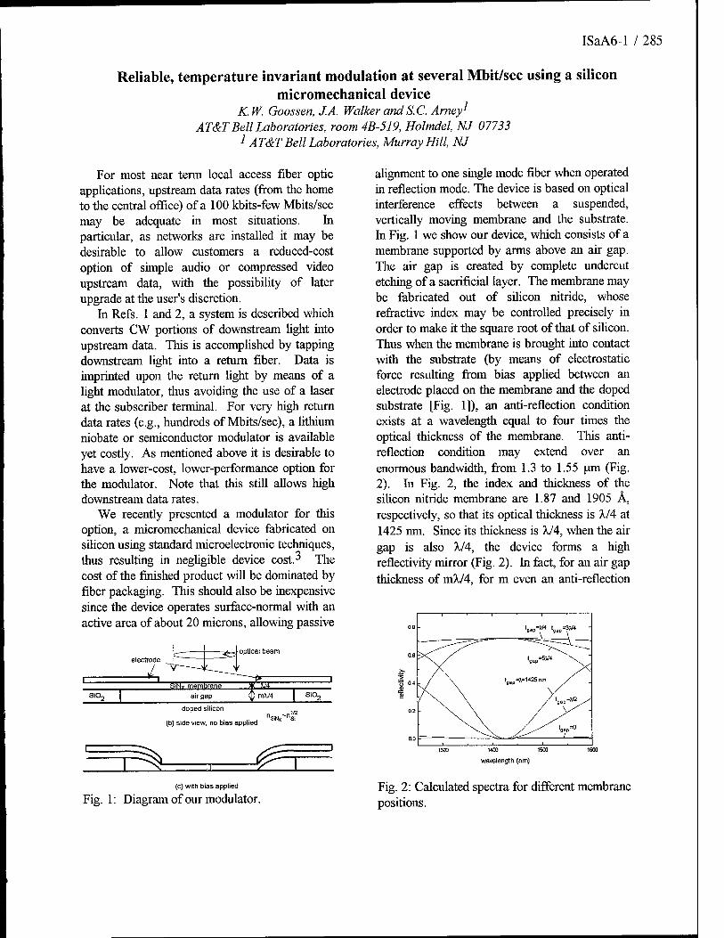
ISaA6-l / 285
Reliable, temperature invariant modulation at several Mbit/sec using a silicon micromechanical device
K.W. Goossen, J.A. Walker andS.C. Amey* AT&T Bell Laboratories, room 4B-519, Holmdel, NJ 07733
1 AT&T Bell Laboratories, Murray Hill, NJ
For most near term local access fiber optic applications, upstream data rates (from the home to the central office) of a 100 kbits-few Mbits/sec may be adequate in most situations. In particular, as networks are installed it may be desirable to allow customers a reduced-cost option of simple audio or compressed video upstream data, with the possibility of later upgrade at the user's discretion.
In Refs. 1 and 2, a system is described which converts CW portions of downstream light into upstream data. This is accomplished by tapping downstream light into a return fiber. Data is imprinted upon the return light by means of a light modulator, thus avoiding the use of a laser at the subscriber terminal. For very high return data rates (e.g., hundreds of Mbits/sec), a lithium niobate or semiconductor modulator is available yet costly. As mentioned above it is desirable to have a lower-cost, lower-performance option for the modulator. Note that this still allows high downstream data rates.
We recently presented a modulator for this option, a micromechanical device fabricated on silicon using standard microelectronic techniques, thus resulting in negligible device cost.3 The cost of the finished product will be dominated by fiber packaging. This should also be inexpensive since the device operates surface-normal with an active area of about 20 microns, allowing passive
optical beam
(b) side view, no bias applied
=SSL Jß
alignment to one single mode fiber when operated in reflection mode. The device is based on optical interference effects between a suspended, vertically moving membrane and the substrate. In Fig. 1 we show our device, which consists of a membrane supported by arms above an air gap. The air gap is created by complete undercut etching of a sacrificial layer. The membrane may be fabricated out of silicon nitride, whose refractive index may be controlled precisely in order to make it the square root ofthat of silicon. Thus when the membrane is brought into contact with the substrate (by means of electrostatic force resulting from bias applied between an electrode placed on the membrane and the doped substrate [Fig. 1]), an anti-reflection condition exists at a wavelength equal to four times the optical thickness of the membrane. This anti- reflection condition may extend over an enormous bandwidth, from 1.3 to 1.55 um (Fig. 2). In Fig. 2, the index and thickness of the silicon nitride membrane are 1.87 and 1905 Ä, respectively, so that its optical thickness is A/4 at 1425 nm. Since its thickness is 1/4, when the air gap is also X/4, the device forms a high reflectivity mirror (Fig. 2). In fact, for an air gap thickness of mA/4, for m even an anti-reflection
'».P=» W=3*
1400 1600
wawslength (nm)
(c) with bias applied
Fig. 1: Diagram of our modulator. Fig. 2: Calculated spectra for different membrane positions.

286 / ISaA6-2
1 %2.00g 2 5.0OV O.OOs 5008/ SB il RUN
FreqC2:>=308.2W-fe RiseC H=132.5ns FallC n = 125.0ns
Fig. 3: Temporal response of our modulator.
condition exists, and for m odd a high reflection exists, although the optical bandwidth decreases for m>l. Hence we call the device the Mechanical Anti-Reflection Switch, or MARS device.
Thus the device may easily handle the optical bandwidth requirements of fiber-in-the-loop applications. In addition it is inexpensive, has no polarization sensitivity, has wide fiber alignment tolerance, projected <1 dB insertion loss (advanced designs) and >20 dB contrast, is chemically and mechanically robust, and as we show here requires no temperature stabilization. We fabricated a device with m~4 (for 1.3 urn), whose membrane is 30x30 microns. The electrode is patterned on the amis and around the rim of the membrane, leaving a 20x20 micron window. The support arms were 20 urn long and 5 um wide. The voltage swing was 25 volts for A/4 deflection. These voltage requirements should decrease greatly by going to m=l. This is because the applied force for a given voltage goes as the inverse of the square of the air gap thickness (since both the capacitance and the electric field increase as the inverse of the gap). Therefore by going to m=l in future devices the voltage requirements should reduce by an order of magnitude.
The temporal response to an applied square wave is shown in Fig. 3. The device is underdamped. The rise time is 130 ns, but it overshoots and rings. A Laplace transfer function relating reflectivity to applied bias
T(s)=(©o2+cf2y[(s+a)2+coo2] models the measured response well. We have indicated in [3] than an appropriate electrical filter inserted between the voltage source and the
device would allow operation without ringing. Thus our prediction is that the device could operate in a digital system at 2 Mbit/sec.
Temperature variation and reliability measurements were performed on a slightly larger device, with a 40x40 micron plate and a 30x30 micron optical window, to facilitate easier measurement. (The temperature sensitivity measurements required use of a lamp/monochromator to take spectra.) The rise time of this device was 350 ns.
This device was modulated at 500 kHz for an extended time period in standard laboratory conditions (no hermetic sealing). It operated for 50 days before failing, or over 2 trillion cycles. The performance of the device was unchanged during this time period. The failure was NOT due to mechanical breakage. The device retained its mechanical structure. Rather, the device failed due to shorting of the electrode. This failure is most likely due to the fact that aluminum was used as the sacrificial layer in the device. The aluminum is undercut under the membrane and support arms, but must be left as a mechanical support under the wire-bond pad. The pressure on the membrane for a given voltage goes as s2/(xj+sx2)2, where 8 is the SiNx relative static dielectric constant, x^ is the thickness of the SiNx, and X2 is the thickness of the air gap. Since under the wire-bond pad, xj is zero (the substrate conducts through the aluminum), the pressure there is 2800 times higher than over the active area of the device. Since enough voltage must be applied to move the membrane, there is an enormous force driving the electrode atoms through the SiNx. This, coupled with the presence of pinholes in the SiNx due to surface roughness of the aluminum, eventually causes shorting. We are attempting to solve this problem by placing additional dielectrics between the wire-bond pad and the SiNx, or by altering the design so that the sacrificial layer is not electrically active, and will report this at a later date.^
Note that this reliability measurement was performed on a modulator wherein the membrane does not ever touch the substrate. For m=l devices, the membrane would impact the substrate, perhaps reducing reliability. This
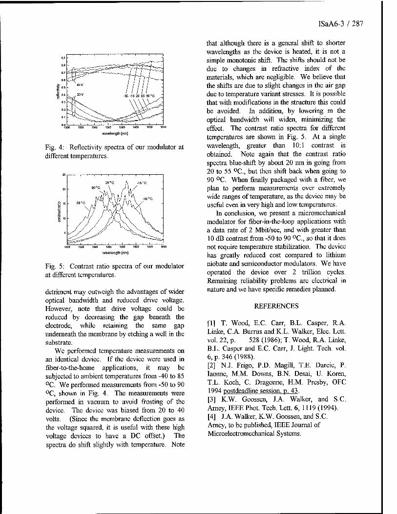
ISaA6-3 / 287
wawslength (nm)
Fig. 4: Reflectivity spectra of our modulator at different temperatures.
1300 1320 1340 1360 1380 1400 1420 1440
wavelength (nm)
Fig. 5: Contrast ratio spectra of our modulator at different temperatures.
detriment may outweigh the advantages of wider optical bandwidth and reduced drive voltage. However, note that drive voltage could be reduced by decreasing the gap beneath the electrode, while retaining the same gap underneath the membrane by etching a well in the substrate.
We performed temperature measurements on an identical device. If the device were used in fiber-to-the-home applications, it may be subjected to ambient temperatures from -40 to 85 °C. We performed measurements from -50 to 90 °C, shown in Fig. 4. The measurements were performed in vacuum to avoid frosting of the device. The device was biased from 20 to 40 volts. (Since the membrane deflection goes as the voltage squared, it is useful with these high voltage devices to have a DC offset.) The spectra do shift slightly with temperature. Note
that although there is a general shift to shorter wavelengths as the device is heated, it is not a simple monotonic shift. The shifts should not be due to changes in refractive index of the materials, which are negligible. We believe that the shifts are due to slight changes in the air gap due to temperature variant stresses. It is possible that with modifications in the structure this could be avoided. In addition, by lowering m the optical bandwidth will widen, minimizing the effect. The contrast ratio spectra for different temperatures are shown in Fig. 5. At a single wavelength, greater than 10:1 contrast is obtained. Note again that the contrast ratio spectra blue-shift by about 20 nm in going from 20 to 55 °C, but then shift back when going to 90 °C. When finally packaged with a fiber, we plan to perform measurements over extremely wide ranges of temperature, as the device may be useful even in very high and low temperatures.
In conclusion, we present a micromechanical modulator for fiber-in-the-loop applications with a data rate of 2 Mbit/sec, and with greater than 10 dB contrast from -50 to 90 °C, so that it does not require temperature stabilization. The device has greatly reduced cost compared to lithium niobate and semiconductor modulators. We have operated the device over 2 trillion cycles. Remaining reliability problems are electrical in nature and we have specific remedies planned.
REFERENCES
[1] T. Wood, E.C. Carr, B.L. Casper, R.A. Linke, CA. Burrus and K.L. Walker, Elec. Lett, vol. 22, p. 528 (1986); T. Wood, RA. Linke, B.L. Casper and E.C. Carr, J. Light. Tech. vol. 6, p. 346 (1988). [2] N.J. Frigo, P.D. Magill, T.E. Darcie, P. Iaonne, M.M. Downs, B.N. Desai, U. Koren, T.L. Koch, C. Dragonne, H.M. Presby, OFC 1994 postdeadline session, p. 43. [3] K.W. Goossen, JA. Walker, and S.C. Arney, IEEE Phot. Tech. Lett. 6, 1119 (1994). [4] JA. Walker, K.W. Goossen, and S.C. Arney, to be published, IEEE Journal of Microelectromechanical Systems.

288 / NOTES
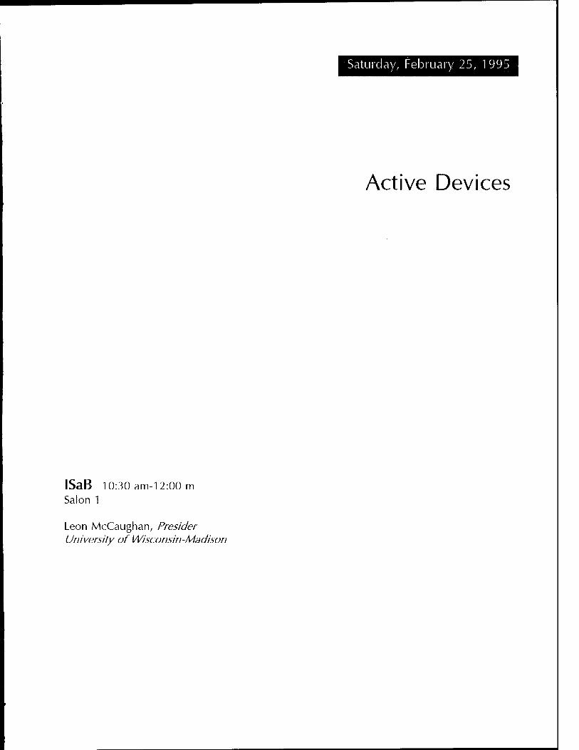
ISaB 10:30 am-12:00 m Salon 1
Saturday, February 25, 1995
Active Devices
Leon McCaughan, Presider University of Wisconsin-Madison

290 / ISaBl-1
Stability and Reliability of Lithium Niobate Optical Modulators Hirotoshi Nagata and Jamshid Nayyer Central Research Laboratories, Sumitomo Osaka Cement Co., Ltd. 585 Toyotomi-cho, Funabashi-shi, Chiba 274, Japan
ABSTRACT The dc and thermal drift phenomena of lithium niobate optical modulators are discussed from the
viewpoints of the device stability and reliability. Further, the engineering procedures to improve and assess these drifts are summarized.
PREVIOUS WORKS The lithium niobate (LN) optical modulators are practically evaluated as the key-devices in optical
communication systems. From this viewpoint, their stable and reliable long-term operations are inevitably desired. The intrinsic problems concerning the stability and reliability of LN modulators are the drift phenomena of the applied bias voltages which depend on the ambient temperature changes and the applied dc bias itself.
The temperature depending drift (thermal drift) was an obstacle in practical uses of the z-cut LN modulator which is the preferred crystal orientation for high-speed communication applications. However, the group in Fujitsu Co., solved this problem by shielding the pyroelectricaly induced charges of the LN crystal surface via Si coating of the device [1]. The thermal drift of the z-cut LN modulators could be further improved by asymmetric design of the Mach-Zehnder waveguide arms, as reported by the authors [2]. In this regard, the use of x-cut LN, exhibiting negligibly small pyroelectric effects, is another answer to avoid the thermal drifts, as observed by many LN device manufacturers.
The bias depending drift (dc drift) phenomenon seems not to be completely eliminated because of the dielectric nature of the materials from which the LN modulator is comprised. The procedures and explanations of reduction of the dc drift have been proposed by Tohoku Univ. group, in which the quality of LN crystal and the chemical deterioration of LN surface due to waveguide formation are reported to affect the magnitude of the dc drift [3]. Further, successful improvements of the dc drift were obtained by the reduction of hydrogen contamination of the LN crystal and formation of less dense Si02 buffer layers [4]. Hydrogen is introduced into the LN crystal as -OH configuration on the O-O plane of LN during the poling process of the crystal which can be effectively reduced by the dry thermal process of Ti in-diffused waveguide-formation instead of the conventional wet process. The dc drift of such hydrogen-reduced LN modulators were reported to be less than half of those of conventional ones [5], In regards to the Si02 buffer layer, low-temperature sputtering and vacuum evaporation techniques, for instance, were reported to result in the dc drift-reduced devices [1], [4]. Further, the dc drifts were observed to be sensitively influenced by the thickness of the buffer layer. These empirical improvements of the fabrication processes might influence the electrical parameters (R and C) of the materials and tend to reduce the dc drift, as explained by the RC circuit model [6].
ANALYSIS OF DC DRIFT PHENOMENA In achievement of reliable operation of the LN modulators, both phenomenological and physical
understanding of the drift mechanisms are needed, which are inevitable in their life-time estimations. Figure. 1 shows the typical dc drift behavior (at 80 °C), which are measured in the Mach Zehnder LN Modulators at the optical wave-length of 1.5 |im, the initial dc bias voltage of 3.5 V and the bias- control frequency of 1 kHz. These modulators are fabricated using the conventional wet Ti-diffusion process and the vacuum evaporation technique in formation of ~1 p.m thick Si02 buffer layer. To avoid the thermal drifts, a thin Si layer is prepared between the buffer layer and the Au electrodes. The two broken curves of Fig. 1 show the results of two different modulators from the same wafer, while the remaining curves are for the ones from the different wafers. During the short-term operation of only 100 hr, the modulators exhibit different dc drifts although the same LN wafer was used. These uneven results can be evidently observed in the dc drift measurements under the fixed dc bias voltages at 5 V, as shown in Fig. 2. After the dc bias application, the dc drifts occur in the opposite (negative) direction to the applied bias, which are followed by the positive drifts. The rates of the negative drifts depend on the modulators themselves. As their origins, the differences in process
ISaBl-2 / 291
parameters such as uncontrolled moist environment, seem to be influential from numerous empirical results, but physical explanations are yet to be given.
Figure. 3 shows the long-term changes of the applied dc biases at 80, 100 and 130 °C of the modulators. Two isothermal drift rates could be distinguished, both being almost constant against the logarithmic operation times. The temperature dependence of these drift rates is shown in Fig. 4 and their activation energies (Ea) are derived to be 0.8 eV for those within 100 hr (circles) and 0.4 eV beyond 100 hr (triangles). Further, the Ea of negative dc drifts occurring within early 10 hr operation (see Fig. 2) was obtained to be 0.5 eV. The positive drifts under the fixed dc bias operation of Fig. 2 gave Ea of 0.9 eV, which is close to 0.8 eV for the corresponding drift in Fig. 3. These results indicate that the dc drift phenomena are due to various origins. One of them could be attributed to the nature of the buffer layer such as its density and -OH contents, because the modulators with the densified and reduced -OH buffer layers, prepared by sputtering deposition technique, exhibit no negative drift. Further, the reduced -OH LN wafers via dry thermal process could provide the modulators with slower drift rates, as shown by the broken curves in Fig. 3, compared with the wet treated ones (solid curves).
NECESSITY FOR SCREENING TESTS In mass production of LN modulators to meet the market demands, the problem is how to maintain
the above mentioned improved stability and reliability of the products. As generally known, both the pure and accurately chemical-doped oxide materials can hardly be achieved unlike semiconductor materials. Fluctuations in hydrogen-contents, refractive indices, electrical resistance etc. are observed in LN wafers, which are examples of such problems in the oxide material-engineering. Therefore, the screening tests concerning the drift phenomena under accelerated conditions become inevitable in addition to those on the optical and electrical performances.
Figures. 5 and 6 show the distributions of the dc drift magnitudes and the thermal drift rates, respectively, in the LN wafers from several lots. The chip numbers on the horizontal axes correspond to the y-direction of the z-cut LN wafer, where each chip-width is about 1 mm. The dc drift voltages in Fig. 5 are obtained by the fixed dc bias (5 V) measurements at 80 °C as the values at 15 min (white marks) and at 90 hr (black marks) after the bias applications. The dc drifts depend on individual wafers, as shown for three different wafers of (a) to (c), with considerably large (10 ~ 20 % of the applied dc bias) magnitudes. The thermal drift rates, measured between 30 and 65 °C, are also broadly distributed in regards to both the same (a) and different wafers (b). The maximum to minimum ratio of these fluctuations is in the range between 3 ~ 1, corresponding to the difference of 3 V within the ordinary operating temperature (0 ~ 70 °C).
As the results, the screening tests are needed to be carried out on all modulators throughout the specified operating temperatures in order to exclude unpredictable chip dependence of the drifts. Prior to these chip-by-chip screening tests, the wafers with reduced dc drifts should be selected by the wafer lot screening tests. For instance, the tests are needed to be carried out at 130 °C for 175 hr to assure the 25-year-operation at 50 °C, where Ea of 1 eV (close to 0.8 ~ 0.9 eV measured) is assumed.
CONCLUSIONS The dc and thermal drift phenomena were discussed as the inherent problems in LN modulators.
Theses drifts originate possibly from the nature of the materials and could not be completely eliminated. However, they can be significantly reduced by engineering improvements and tests to exclude the undesired ones. Such screening tests are inevitable in the present LN modulators to assure their stable and reliable operations.
REFERENCES [1] M.Seino et. al., Proc. of the OFC'92 (San Jose, CA), February 8-11, 1992, pp. 325-328. [2] J.Nayyer and H.Nagata, IEEE Photonics Technology Lett., vol.6, pp. 952-955. [3] M.Minakata et. al., Tech. Digest of the OEC'94 (Chiba, Jpn), July 12-15, 1994, pp. 19-21, PDII-3. [4] H.Nagata et. al., J. Appl. Phys., vol.73, pp. 1405-1408, 1994. [5] H.Nagata et. al., Appl. Phys. Lett., vol.64, pp. 1180-1182, 1994. [6] S.Yamada and M.Minakata, Jpn. J. Appl. Phys., vol.20, pp. 733-735, 1981.
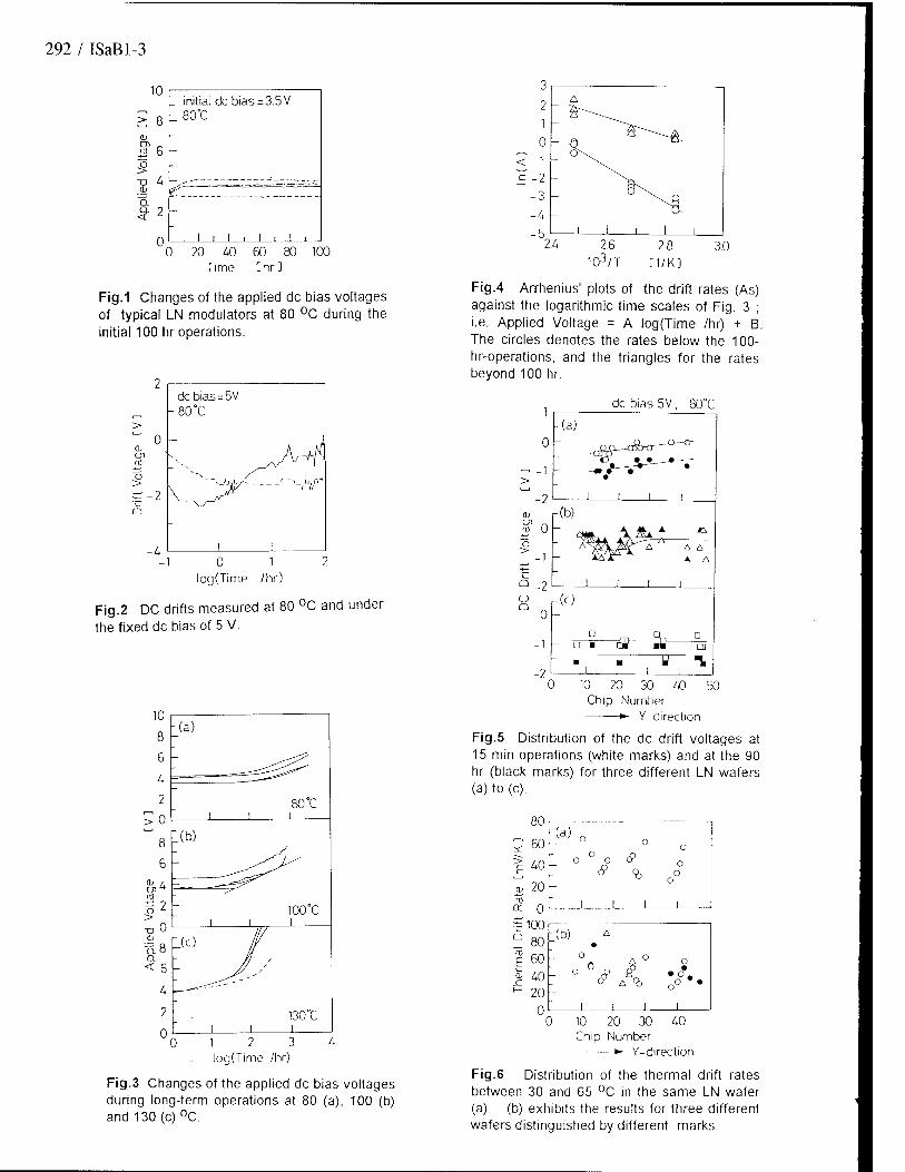
292 / ISaBl-3
0 20 40 60 80 100 Time Ehr]
Fig.1 Changes of the applied dc bias voltages of typical LN modulators at 80 °C during the initial 100 hr operations.
103/T
Fig.4 Arrhenius' plots of the drift rates (As) against the logarithmic time scales of Fig. 3 ; i.e. Applied Voltage = A log(Time /hr) + B. The circles denotes the rates below the 100- hr-operations, and the triangles for the rates beyond 100 hr.
dc bias 5V. "C
log(Time /hr)
Fig.2 DC drifts measured at 80 °C and under the fixed dc bias of 5 V.
0
,—, -1 > 1 1
-2
en -5 0 o > i
Q -2
O 0-
-(a)
- <%^fT^Z -
-mrf • • 1 1 1 i
r(b)
: 1 •u A%^— t\
M^ A A
- 1 1 1
A A
1
|-(C)
- D D D
CD - □ ■ i:a aU
■ i i i 1
10 20 30 40 Chip Number >- Y-direction
50
Fig.5 Distribution of the dc drift voltages at 15 min operations (white marks) and at the 90 hr (black marks) for three different LN wafers (a) to (c).
60
40
20
"(a) o o o o o
n 6> o o
o - 6> %
I l I I
0 1 2 3 log(Time /hr)
Fig.3 Changes of the applied dc bias voltages during long-term operations at 80 (a), 100 (b) and 130(c)°C.
10 20 30 40 Chip Number »- Y-direction
Fig.6 Distribution of the thermal drift rates between 30 and 65 °C in the same LN wafer (a), (b) exhibits the results for three different wafers distinguished by different marks.

ISaB2-l / 293
Polarization - independent Electrooptic Depolarizer F. Heismann and K. L. Tokuda
AT&T Bell Laboratories, 101 Crawfords Corner Road, Holmdel, NJ 07733-3030
INTRODUCTION - Optical depolarizers are frequently used in optical measurement equipment as well as in fiberoptic sensors to remove undesired polarization sensitivity [1]. Recently, depolarizers have also been employed in long-haul all-optical communication systems to avoid polarization hole burning (anisotropic gain saturation) in the erbium-doped fiber amplifiers (EDFA) caused by the optical information carrier [2]. Although the difference in polarization-dependent gain is small [3], it accumulates in each amplifier stage and severely impairs the optical signal-to-noise ratio (SNR) in transoceanic cables spanning distances of up to 9000 km [4]. These undesired SNR impairments can be removed by modulating (scrambling) the state of polarization (SOP) of the optical carrier faster than the time constant of polarization hole burning, fs~0.1 ms [5], such that, averaged over ts, all possible polarization states are excited with equal probability [2], [6].
In this paper we report an optically broadband polarization modulator that depolarizes an optical carrier independent of its SOP. The electrooptic depolarizer operates with a single-mode waveguide on low- birefringent x-cut z-propagation lithium niobate (LiNb03) and acts like a combination cascade of rotating half-wave and quarter-wave plates. It produces highly depolarized light with <3% residual degree of polarization, negligible intensity modulation of <1.6%, and variable depolarization times in the us to ms range.
OPERATION - Polarized light with unknown or fluctuating SOP can be depolarized by a combination cascade of a rotating half-wave plate (HWP) and a rotating quarter-wave plate (QWP) [7]. Complete depolarization is achieved when the time averages of the three Stokes parameters S,, S2 and S3 vanish simultaneously, i.e. when the degree of polarization
ts and S0 is the total optical power.
Assuming that the input light to the depolarizer is completely polarized (DOP=1), we can describe the operation of the depolarizer by a 3x3 reduced Mueller matrix M, which relates the three-dimensional Stokes vector tout = (S10ut, S2out, S3olrf/ of the output SOP to that of the input SOP, 3ln = (S1ln,S2in,S3in)
t. A rotating HWP spinning at constant angular velocity Q-,/2 followed by a QWP spinning at angular velocity Q.2/2 is described by the matrix
M=-
COS (2Q.1 fJ + COS (2AQ.t),
s\n(2ü.1t)+s\n(2Ailt),
2sin(£2,f-M2fJ,
DOP = ^<ST>2 + <S2>2 + <S3>
2 /S0 = 0,
where the brackets denote time averaging over
-s\n(2Q.1t)+s'm(2AD.t), -2sin(Q.2t)
-COS (2Q.1 fj+cos (2A£lt), 2cos (Q.2t)
-2cos(£l1t-AQ.t), 0
where AQ=£22-Q, [7]. Polarization- independent depolarization with DOP=Q is obtained when all elements M,j of M vanish in time average. It is easily verified that for ATi^O, except for Aü,=Q.1t <M;y>=0 for all /,/= 1,2, 3. Hence, the output light is depolarized for any arbitrary input SOP. Fig. 1 shows an example of the trace of the modulated output SOP for 45° linear input SOP and ß,= 7.5ft2 (HWP spins at 1.5 times the speed of QWP).
IMPLEMENTATION - The electrooptic depolarizer, shown schematically in Fig. 1, is fabricated on low-birefringence x-cut, z- propagation LiNb03 and operates with a standard titanium-indiffused strip waveguide that is directly butt-coupled to single-mode fibers with 4.4 dB fiber-to-fiber insertion loss and negligible polarization dependence (<0.1 dB) at 1.5 u.m wavelength. The depolarizer is designed for modulation in the 1 kHz to 1 MHz range and comprises three succeeding electrode sections acting as a rotating zero-order QWP, HWP, and QWP, respectively, similar to the polarization transformer reported in [8]. The second QWP
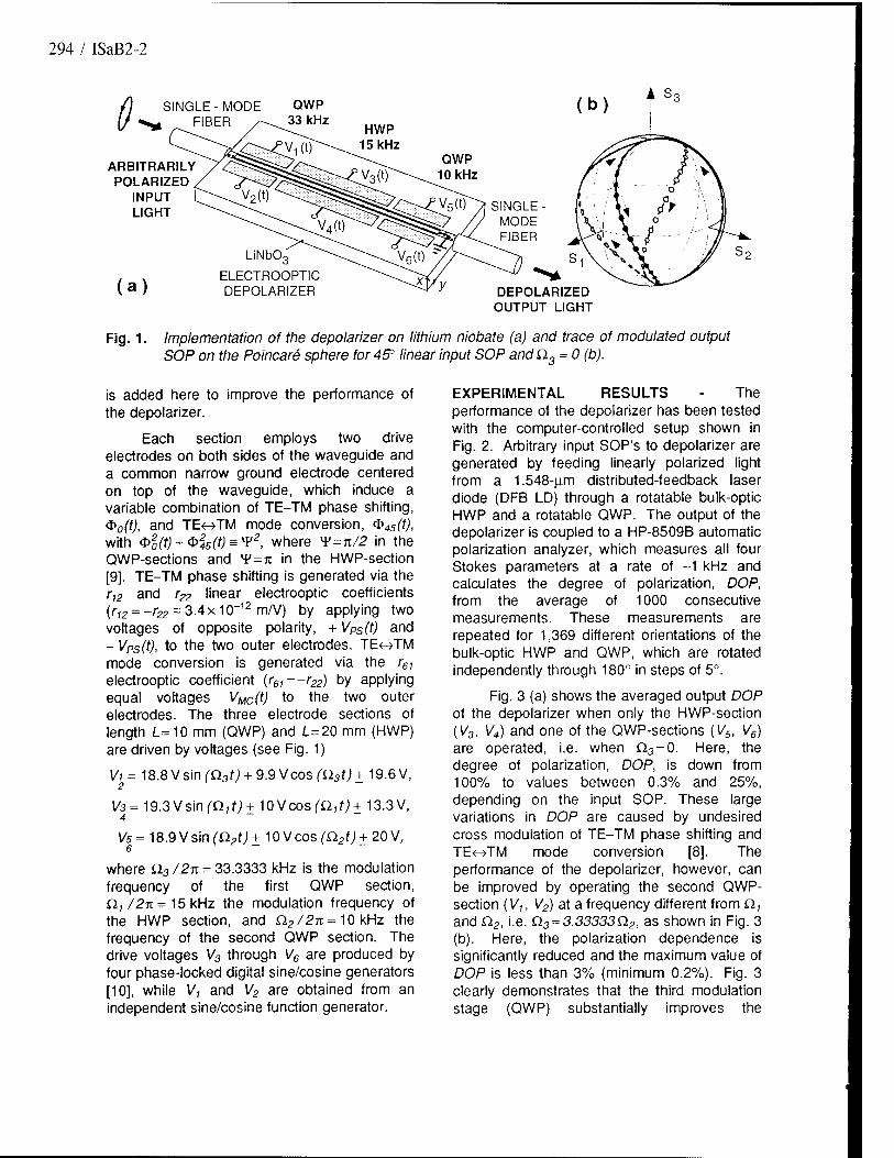
294 / ISaB2-2
9 SINGLE-MODE , FIBER
QWP 33 kHz
HWP 15 kHz
ARBITRARILY POLARIZED
INPUT LIGHT
QWP 10 kHz
(a)
LiNbO, ELECTROOPTIC DEPOLARIZER
SINGLE MODE FIBER
DEPOLARIZED OUTPUT LIGHT
Fig. 1. Implementation of the depolarizer on lithium niobate (a) and trace of modulated output SOP on the Poincare sphere for 45? linear input SOP and Q.3 = 0 (b).
is added here to improve the performance of the depolarizer.
Each section employs two drive electrodes on both sides of the waveguide and a common narrow ground electrode centered on top of the waveguide, which induce a variable combination of TE-TM phase shifting, <J>0ffJ, and TE<H>TM mode conversion, <£>45(t), with <S>20(t) + <b245(t) = ^2, where x¥=n/2 in the QWP-sections and *¥=n in the HWP-section [9]. TE-TM phase shifting is generated via the r12 and r22 linear electrooptic coefficients (r,2 = -r22 = 3.4x1(r12 m/V) by applying two voltages of opposite polarity, + VPS(t) and - VPs(t), to the two outer electrodes. TEoTM mode conversion is generated via the r61
electrooptic coefficient {r61=-r22) by applying equal voltages VMC(t) to the two outer electrodes. The three electrode sections of length L=10 mm (QWP) and L=20 mm (HWP) are driven by voltages (see Fig. 1)
Vi = 18.8V s\n(Q.3t)±9.9V cos (C23t)± 19.6V,
V3= ^9.3Vs\n(n1t)±■\0Vcos(Cl1t)± 13.3V, 4
Vs = 18.9Vsin(Cl2t)+ 10 Vcos (Cl2t) ±20 V, 6
where £23 /2n = 33.3333 kHz is the modulation frequency of the first QWP section, Q1 /27t=15kHz the modulation frequency of the HWP section, and Q2/27t=10kHz the frequency of the second QWP section. The drive voltages V3 through V6 are produced by four phase-locked digital sine/cosine generators [10], while V1 and V2 are obtained from an independent sine/cosine function generator.
EXPERIMENTAL RESULTS - The performance of the depolarizer has been tested with the computer-controlled setup shown in Fig. 2. Arbitrary input SOP'S to depolarizer are generated by feeding linearly polarized light from a 1.548-um distributed-feedback laser diode (DFB LD) through a rotatable bulk-optic HWP and a rotatable QWP. The output of the depolarizer is coupled to a HP-8509B automatic polarization analyzer, which measures all four Stokes parameters at a rate of ~1 kHz and calculates the degree of polarization, DOP, from the average of 1000 consecutive measurements. These measurements are repeated for 1,369 different orientations of the bulk-optic HWP and QWP, which are rotated independently through 180° in steps of 5°.
Fig. 3 (a) shows the averaged output DOP of the depolarizer when only the HWP-section (V3, V4) and one of the QWP-sections (V5, V6) are operated, i.e. when £i3 = 0. Here, the degree of polarization, DOP, is down from 100% to values between 0.3% and 25%, depending on the input SOP. These large variations in DOP are caused by undesired cross modulation of TE-TM phase shifting and TE<H>TM mode conversion [8]. The performance of the depolarizer, however, can be improved by operating the second QWP- section {V1t V2) at a frequency different from Q, and Q.2, i.e. Cl3 = 3.33333D.2, as shown in Fig. 3 (b). Here, the polarization dependence is significantly reduced and the maximum value of DOP is less than 3% (minimum 0.2%). Fig. 3 clearly demonstrates that the third modulation stage (QWP) substantially improves the

ISaB2-3 / 295
£L 1.548 (im
DFB LASER
ROTATABLE HWP QWP
o- n A\* •0'
LINEAR POLARIZER
n. SIN /COS
±1 i ii ii i
£L ELECTROOPTIC DEPOLARIZER
tf POLARIZATION
ANALYZER
COMPUTER
Fig. 2. Experimental test setup for the performance evaluation of the depolarizer.
180°
„ 25
- 12.5 DL O Q
180°
0° 0°
Fig. 3. Degree of output polarization (DOPJ versus input SOP for Q.3 = 0 (a) and Q.3/2n = 33.3333 kHz (b).
performance of the depolarizer. The modulation frequencies in Fig. 3 have been chosen arbitrarily and may be changed to other values in the kHz to MHz range [10]. Moreover, unlike the narrowband acoustooptic depolarizer reported in [11], our broadband electrooptic depolarizer can be operated over an optical bandwidth of at least 10 nm without having to readjust the drive voltages [8], [9].
Using a fast PIN photo diode to measure undesired intensity modulation in the output of the depolarizer, we find maximum peak-to-peak intensity fluctuations of less than 1.6% (-18 dB), which are caused by the small polarization-dependent insertion loss.
REFERENCES
[1] M. M. Howerton and W. K. Burns, IEEE Photon. Technol. Lett. 6, p. 115, 1994.
[2] M. G. Taylor, IEEE Photon. Technol. Lett. 5, p. 1244, 1993.
[3] V. J. Mazurczyk and J. L. Zyskind, IEEE Photon. Technol. Lett. 6, p. 616, 1994.
[4] F. Bruyere and O. Audouin, IEEE Photon. Technol. Lett. 6, p. 654,1994.
[5] N. S. Bergano, Conf. Optical Fiber Communication 1994, Paper FF4, p. 305.
[6] V. Letellier, G. Bassier, P. Marmier, R. Mohn, R. Uhel, and J. Artur, Electron. Lett. 30, p. 589, 1994.
[7] B. H. Billings, J. Opt. Soc. Am. 41, p. 966, 1951.
[8] F. Heismann and M. S. Whalen, Electron. Lett. 27, p. 377, 1991.
[9] F. Heismann, J. Lightwave Technol. 12, p. 690, 1994.
[10] F. Heismann and M. S. Whalen, IEEE Photon. Technol. Lett. 4, p. 503, 1992.
[11] R. Noe, M. Rehage, C. Harizi, and R. Ricken, Electron. Lett. 30, p. 1500, 1994.
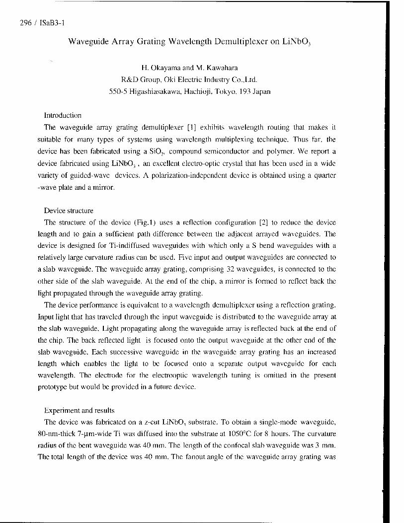
296 / ISaB3-l
Waveguide Array Grating Wavelength Demultiplexer on LiNb03
H. Okayama and M. Kawahara
R&D Group, Oki Electric Industry Co.,Ltd.
550-5 Higashiasakawa, Hachioji, Tokyo, 193 Japan
Introduction
The waveguide array grating demultiplexer [1] exhibits wavelength routing that makes it
suitable for many types of systems using wavelength multiplexing technique. Thus far, the
device has been fabricated using a Si02, compound semiconductor and polymer. We report a
device fabricated using LiNb03, an excellent electro-optic crystal that has been used in a wide
variety of guided-wave devices. A polarization-independent device is obtained using a quarter
-wave plate and a mirror.
Device structure
The structure of the device (Fig.l) uses a reflection configuration [2] to reduce the device
length and to gain a sufficient path difference between the adjacent arrayed waveguides. The
device is designed for Ti-indiffused waveguides with which only a S bend waveguides with a
relatively large curvature radius can be used. Five input and output waveguides are connected to
a slab waveguide. The waveguide array grating, comprising 32 waveguides, is connected to the
other side of the slab waveguide. At the end of the chip, a mirror is formed to reflect back the
light propagated through the waveguide array grating.
The device performance is equivalent to a wavelength demultiplexer using a reflection grating.
Input light that has traveled through the input waveguide is distributed to the waveguide array at
the slab waveguide. Light propagating along the waveguide array is reflected back at the end of
the chip. The back reflected light is focused onto the output waveguide at the other end of the
slab waveguide. Each successive waveguide in the waveguide array grating has an increased
length which enables the light to be focused onto a separate output waveguide for each
wavelength. The electrode for the electrooptic wavelength tuning is omitted in the present
prototype but would be provided in a future device.
Experiment and results
The device was fabricated on a z-cut LiNb03 substrate. To obtain a single-mode waveguide,
80-nm-thick 7-|im-wide Ti was diffused into the substrate at 1050°C for 8 hours. The curvature
radius of the bent waveguide was 40 mm. The length of the confocal slab waveguide was 3 mm.
The total length of the device was 40 mm. The fanout angle of the waveguide array grating was

ISaB3-2 / 297
31 x 0.003 rad. The path length difference between successive waveguides was 17 (im. The end
of the chip was polished flat with a precision exceeding a quarter of the wavelength. Figures
2(A) and (B) show the measured spectral response of the device. Fig. 2(A) shows the response
for the TM mode excitation, and Fig. 2(B) is for the TE mode excitation in the middle waveguide
of the input and output array. Crosstalk ranged from -12 to -25 dB. The full width at half
maximum of the transmission peak was 1 nm.
Polarization-independent device
A quarter-wave plate pasted on a Au-mirror-evaporated substrate (reflective quarter
wave-plate) was used (Fig.3), instead of a mirror at the edge of the chip to achieve polarization
independence. The quarter-wave plate was antireflection coated. The reflective quarter-wave
plate converts the TM (TE) polarization that has been propagated from the input port into the TE
(TM) polarization and reflects the light back toward the output port at the end of the chip. The
two orthogonal input polarizations experience the same refractive index and optical path as the
light travel through the device, thus achieving polarization independence. The quarter-wave plate
was 50 |im thick. The index-matching fluid was inserted between, the edge of the chip and the
reflective quarter-wave plate, with the resultant reflectivity at the interface between the chip and
the quarter-wave-plate being -14 dB. The reflectivity at this interface can be reduced further
using an antireflection coating at the edge of the chip. The measured results (Fig.4) showed the
transmission peak to be at the middle between those of the TM and the TE polarization of the
device without the reflective quarter-wave plate. The side lobe around the transmission peak is
due to the residual reflection at the interface between the chip and the quarter-wave-plate. A -6
dB excess loss from the reflective quarter-wave plate was deduced from this result, and total
device loss was 20 dB.
Conclusion
We demonstrated a wavelength demultiplexer using LiNb03. The full width at half maximum
of the transmission peak was 1-2 nm. The crosstalk ranged from -12 dB to -25 dB. We
proposed a polarization independent device employing a quarter-wave plate and a mirror.
References
[1] H.Takahashi et al., J. Lightwave Tech., vol. 12, p. 989, 1994.
[2] M. Ziringbil et al., IEEE Photon. Tech. Lett., vol. 6, p. 516, 1994.
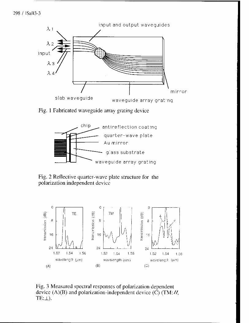
298 / ISaB3-3
nput and output waveguides
slab waveguide mirror
waveguide array grating
Fig. 1 Fabricated waveguide array grating device
C'1^P .- antireflection coating
quarter-wave plate
Au mirror
glass substrate
waveguide array grating
Fig. 2 Reflective quarter-wave plate structure for the polarization independent device
m X!
16 -
24
1.52 1.54 1.56
wavelength (|im)
m "a
1.52 1.54 1.56
wavelength (iim)
(A) (B)
1.52 1.54
wavelength
1.56
(urn)
(C)
Fig. 3 Measured spectral responses of polarization dependent device (A)(B) and polarization-independent device (C) (TM: //, TE:_L).

ISaB4-l / 299
Passband Engineering of Acousto-Optic Filters
Janet L. Jackel, Bellcore, Red Bank, NJ 07701 Phone: (908) 758-3147 FAX: (908) 758-4372
and David A. Smith, Case Western Reserve University, Cleveland, OH
Phone: (216) 368-4073 FAX (216) 368-2688
Introduction: The acousto-optic filter (AOTF) or switch has unique features which make it a valuable tool for optical wavelength selection. In particular, the ability to select several wavelengths simultane- ously suggests that the AOTF may be used as the basis for a tunable wavelength routing switch. How- ever, passbands of existing filters are not as flat as desired for applications requiring the use of several concatenated filters or where the wavelength to be switched is not well defined. In this paper we de- scribe variant filter designs which provide substan- tially flattened passbands at modest cost in power and length and which can be implemented using extensions of known techniques. One of these de- signs has been tested experimentally and is shown to perform as simulations lead us to expect.
The AOTF consists of collinear optical and acoustic waveguides arranged in such a way that the acousto-optic interaction couples the two orthogonal polarizations of the optical waveguide. The resulting polarization transformation is wavelength depend- ent, and is a function of both the birefringence of the optical waveguide and the acoustic frequency. Po- larization transformation is the basis of either filter- ing, when external or on-chip polarizers are added, or switching, when polarizing beamsplitters are used. (When the original polarization is selected the device is said to be in the bar state, and when the orthogonal polarization is selected, the switch is in the cross state. In the absence of an acoustic wave, the device remains in the bar state for all wave- lengths.)
A major shortcoming of currently demon- strated AOTFs is their non-ideal passband. An AOTF in which the coupling coefficient (proportional to the amplitude of the acoustic wave) is constant has the familiar sin2(x)/x2 transmission function for the cross state. In addition to a high out- of-band transmission, with about -9 dB for the first sidelobe (the effects of which can be reduced using a dilated switch1) the passband of this filter is far from flat. As a consequence, when several identical filters are concatenated, as may be necessary in a large
network, the resulting compounded passband be- comes narrower, and may challenge the wavelength stability of the sources. The consequences of a non- flat passband are even greater for the bar state, since a small cross state loss corresponds to an unaccepta- bly large bar state crosstalk. For example, a loss of 0.5 dB in the cross state creates a bar state crosstalk of-10 dB.
The basic AOTF filter response has been improved by tapering the strength of the acousto- optic interaction to produce the apodized filter.2 If the acoustic wave is introduced into a SAW waveguide adjacent to and identical to the one over- lying the optical waveguide, the acoustic wave cou- ples from one acoustic waveguide to the other. The amplitude of the acoustic wave, and therefore the coupling coefficient, K, at the position x in the sec- ond waveguide is proportional to sin(2nx/Lc) where Lc is the acoustic coupling length; Lc is dependent on both the structure of the individual acoustic waveguides and on their separation. If the acousto- optic interaction takes place over a length Lx = Lc/2 (with the acoustic wave absorbed after this distance) sidelobes are reduced substantially, to a theoretical value of about -17 dB for the first sidelobe. The re- sulting passband is somewhat wider, but still far from flat.
A more sophisticated tapering function, re- lated to the Butterworth filter function used in elec- tronics, has recently been proposed.3 Calculations show that a nearly-ideal passband would be obtained for an acousto-optic interaction amplitude given by this taper function. But at present there appears to be no simple way to realize such a filter function, which requires an oscillating and decaying acoustic amplitude, with a tapered onset. Thus, it is useful at this time to examine somewhat simpler taper func- tions which can be achieved using extensions of known techniques. Device Simulations: We have investigated two simpler taper functions, both of which can flatten the AOTF passband substantially. Both require absorp- tion of the acoustic wave, but neither is highly sensi-
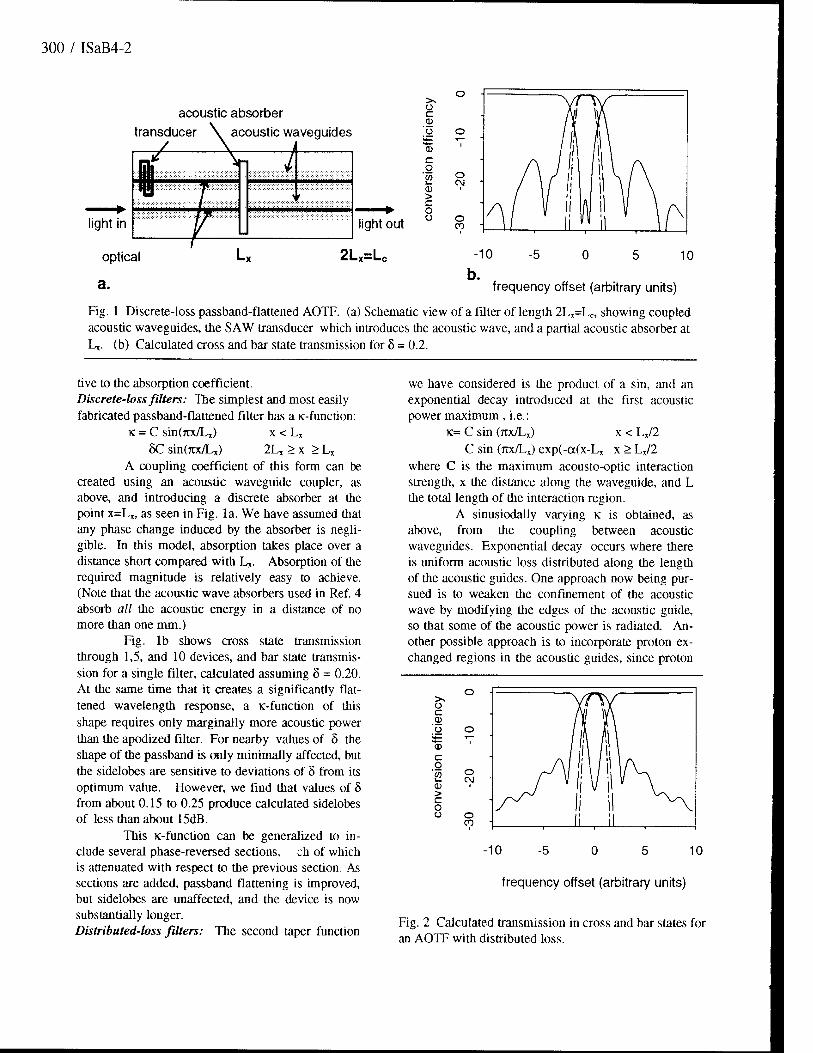
300 / ISaB4-2
acoustic absorber transducer \ acoustic waveguides
light in
J- -1
light out
optical 2Lx=Le
>-. O c CD ü o
4= *~ CD c o CO o i_ CM CD 1
> c o u o
CD
-10 10
frequency offset (arbitrary units)
Fig. 1 Discrete-loss passband-flattened AOTF. (a) Schematic view of a filter of length 2LX=LC, showing coupled acoustic waveguides, the SAW transducer which introduces the acoustic wave, and a partial acoustic absorber at Lx. (b) Calculated cross and bar state transmission for 8 = 0.2.
tive to the absorption coefficient. Discrete-loss filters: The simplest and most easily fabricated passband-flattened filter has a K-function:
K = C sin(jrx/Lx) x < Lx
5C sin(7Cx/Lx) 2LX > x > Lx
A coupling coefficient of this form can be created using an acoustic waveguide coupler, as above, and introducing a discrete absorber at the point x=Lx, as seen in Fig. la. We have assumed that any phase change induced by the absorber is negli- gible. In this model, absorption takes place over a distance short compared with Lj. Absorption of the required magnitude is relatively easy to achieve. (Note that the acoustic wave absorbers used in Ref. 4 absorb all the acoustic energy in a distance of no more than one mm.)
Fig. lb shows cross state transmission through 1,5, and 10 devices, and bar state transmis- sion for a single filter, calculated assuming 8 = 0.20. At the same time that it creates a significantly flat- tened wavelength response, a K-function of this shape requires only marginally more acoustic power than the apodized filter. For nearby values of 8 the shape of the passband is only minimally affected, but the sidelobes are sensitive to deviations of 8 from its optimum value. However, we find that values of 8 from about 0.15 to 0.25 produce calculated sidelobes of less than about 15dB.
This K-function can be generalized to in- clude several phase-reversed sections, ch of which is attenuated with respect to the previous section. As sections are added, passband flattening is improved, but sidelobes are unaffected, and the device is now substantially longer. Distributed-loss filters: The second taper function
we have considered is the product of a sin, and an exponential decay introduced at the first acoustic power maximum, i.e.:
K= C sin (7tx/Lx) x < Lx/2 C sin (TTX/LX) exp(-a(x-Lx x > Lx/2
where C is the maximum acousto-optic interaction strength, x the distance along the waveguide, and L the total length of the interaction region.
A sinusiodally varying K is obtained, as above, from the coupling between acoustic waveguides. Exponential decay occurs where there is uniform acoustic loss distributed along the length of the acoustic guides. One approach now being pur- sued is to weaken the confinement of the acoustic wave by modifying the edges of the acoustic guide, so that some of the acoustic power is radiated An- other possible approach is to incorporate proton ex- changed regions in the acoustic guides, since proton
>. o c CD 'o it:
CD
C g 'c/5 k. CD > C o o
o CM
O CO
-10 -5 0 5 10
frequency offset (arbitrary units)
Fig. 2 Calculated transmission in cross and bar states for an AOTF with distributed loss.

ISaB4-3 / 301
exchange has been shown to create acoustic loss. Fig. 2 shows calculated transmission of
such a filter, with length 2Lx. Distributed-loss de- vices give flattening similar to that for a discrete-loss device of the same length, but with a distributed ab- sorber, the fabrication tolerances defining Lx are relaxed, and it is not even necessary to know L* in order to obtain a flattened filter. (However, since the width of the passband is defined by Lx, control of channel width determines the required Lx.) Sidelobe reduction: As our comparison of devices having differently length implies, the techniques used to flatten the filter have little effect on side- lobes, and these two goals must be approached inde- pendently. In general, sidelobes can be reduced in any of these filters by tapering the onset of the acousto-optic interaction. The simplest example is the apodized filter, in which the tapering reduces the first sidelobe from -9 to -17 dB. While any tapering method will provide some reduction of sidelobes, tapers typically make the device longer.
Design Summary: Some general rules for designing any of the passband-flattened AOTFs are:
•The basic 3-dB passband is determined by Lx,; for any given type of filter the product of the passband and Lx is constant.
•The required acoustic power for a given filter design is proportional to 1/LX
2. Longer devices require much less power.
•Adding sections with phase-reversed acoustic amplitude improves flattening, but im- provement is marginal when more than two sections are used.
•Tapering the onset of the acousto-optic interaction lowers sidelobes, but also increases de- vice length.
Implementation: The discrete-loss filter, with length ~2LX is the first and currently the only one of these AOTFs to have been tested.5 This filter offers a usable combination of passband flatness and side- lobe intensity, as seen in Fig. 3, at the cost of only modest increases in length and acoustic power. In addition, this device was constructed using known fabrication techniques, with photoresist used as the partial acoustic absorber. Measurements using a range of values for 6 and device lengths indicate that the filter behavior is in good agreement with the simulations presented here. Implementation of dis- tributed-loss designs will require the development of lossy acoustic waveguides, an approach which is being pursued at this time, as is the design of acous- tic waveguide tapered couplers.
Y Y
/' \ / \ A r \l \ A
\
„ -49
§ -59 CO CO
I -69 c CO
^-79 1538.9 1548.9
Wavelength [nm]
Fig. 3 Measured cross and bar state transmission for a discrete-loss AOTF with length 2LX, Lx = 17 mm, and 5 = 0.15.
Acknowledgment: This work was sup- ported in part by the Advanced Research Projects Agency (ARPA).
References
1. D. A. Smith, A. d'Alessandro, J. E. Baran, D. J. Fritz, and R. H. Hobbs, "Reduction of cross talk in an acousto-optic switch by means of dilation," Opt. Lett. 19,99-101(1994). 2. H. Hermann and St. Scmidt, " Integrated acousto- optical mode-converters with weighted coupling us- ing surface acoustic wave directional couplers," Electron. Lett. 28, 979-980 (1992)D. A. Smith and J. J. Johnson, "Sidelobe suppression in an acousto-optic filter with a raised-cosine interaction strength," Appl. Phys. Lett. 61, 1025-1027 (1992). 3. G. H. Song, "Proposal for an acousto-optic filter with a near-ideal bandpass spectrum," Integrated Photonics Research . 1994 Technical Digest Series, Vol. 4,238-240 (Optical Society of America, 1994). 4. H. Hermann, P. Müller-Reich, V. Reimann, R. Ricken, H. Siebert, and W. Sohler, "Integrated, TE- and TM-Pass, Acoustically Tunable, Double-Stage Wavelength Filters with Combined Opti- cal/Acoustical Waveguides," IPR'92, Paper ME3. 5. J. L. Jackel, J. E. Baran, A. d'Alessandro, and David A. Smith, "A passband-flattened acousto- optic filter," submitted to Photonics Technology Letters.

302 / ISaB5-l
High-Speed Directional Coupler Modulator in AlGaAs with Capacitively Loaded Electrode Structure
Mark Yu and Anand Gopinath
Department of Electrical Engineering University of Minnesota Minneapolis, MN 55455
Tel: (612)625-3841
An electrode structure for the directional coupler modulator based on the capacitive- loaded design was designed, as shown in Figure 1, where the RF signal line and ground plane are placed on either side of optical waveguides and connected to the electrodes on top of the ridges through 50 |im wide air-bridges. The impedance matching, and tapers, are designed using the constant impedance in coplanar waveguide. As the RF signal is applied to one end of the elec- trode, it travels through the side electrode which has the capacitance Cd, and because it is con- nected to the electrode on top of the ridge, additional lump capacitance Cd' will be added to the structure, as shown in Figures 2a and 2b. Thus, the effective microwave index, ^Breff, for the ca- pacitive-coupled electrode becomes
»* = fW (1) and the microwave phase velocity is
vrf = -^~ (2) 1 neff where co is the velocity of light in vacuum. We may show this electrode structure as a matched RF transmission line, shunted by parallel capacitances. This additional lumped capacitance added to the line results in an artificial transmission line, with a cutoff frequency, and thus a re- duction of the rf bandwidth. Three different optical modulators using capacitive-loaded electrode with one coupling length 2500 |im were designed based on different values of S and W for the gap G=2 |im. Their effective microwave index and impedance are calculated and summarized in Table 1.
The calculated RF effective indices in Table 1 suggest that the slow-wave effect may be enhanced by moving the RF signal line close to the ridge, and using large width of RF signal line. With the capacitve-loaded design, we can improve the velocity match by 40%, however, with a further reduction of the cutoff of the RF bandwidth. We have simulated the small-signal relative response [1,2] of the first case in Table 1, W= 6 u.m and S= 20 Jim, biased in the linear region of the transfer function for several different frequency-dependent losses, and is shown in Figures 3. The results predict that for the transmission line loss less than 2 dB/cm, half power bandwidth is about 23 GHz, and for 4 dB/cm, the 3 dB bandwidth is about 20 GHz.
Figure 4 shows the measured phase response of the electrode for W= 6(im, 10|im, and 20 |im compared with the referenced phase response of a uniform line which has effective index neff = "J(eTeff+l)/2, where Zf= 13 for GaAs. The referenced phase is determined by multiplying the RF propagation constant with the line length which is approximately 3600 Jim, including 2500 (im interaction length and the input and output sections. It can be seen that the rate of change in phase with repect to frequency is higher for the capacitively loaded structures. As we calculate

ISaB5-2 / 303
the RF phase velocity slowing factor, we consider only the section where the electrical signal interacts with the optical wave, which is 2500 Jim long. Therefore, the electrical length of input and output sections should be subtracted from the measured phase delay. As an example, for the case of W=20u.m, the measured phase delay is 195° at 15.27 GHz, and the subtracted result is 142°, whereas the phase delay is 121° for 2500 Jim length reference line. Since the ratio of phase velocity is inversely proportional to the ratio of phase response, the velocity reduction is there- fore found to be 0.85 and the effective index is then V7/0.85= 3.11. This proves that a slow- wave effect occurs in this capacitive-loaded electrode design. The measured bandwidth of the modulator with 2500 |im interation length for electrode widths W= 20 u.m by extrapolation, shown in Figure 5, was obtained to be approximately 17 GHz, which is the highest bandwidth obtained in directional coupler modulators.
References 1. J. P. Donnelly and A. Gopinath, "A comparison of power requirements of traveling-wave
LiNb03 optical couplers and interferometric modulators," IEEEJ. Quantum Electron., vol. QE-23, 1987.
2. S. K. Koroky and R. C. Alferness, "Time and frequency-domain response of directional- coupler traveling-wave optical modulators," J. Lightwave Technol., Vol. 1, pp. 244-251, 1983.
Figure 1 The optical modulator design with capacitive-loaded electrode structure
RFSom
w
Ground
GaAs/AlGaAs
(a) Loaded ^d
Capacitance
GaAs/AlGaAs
(b) Figure 2 Cross section of capactive-loaded electrode, (a) capacitance of signal
electrode, (b) loading capacitance resulting from ridge electrodes.
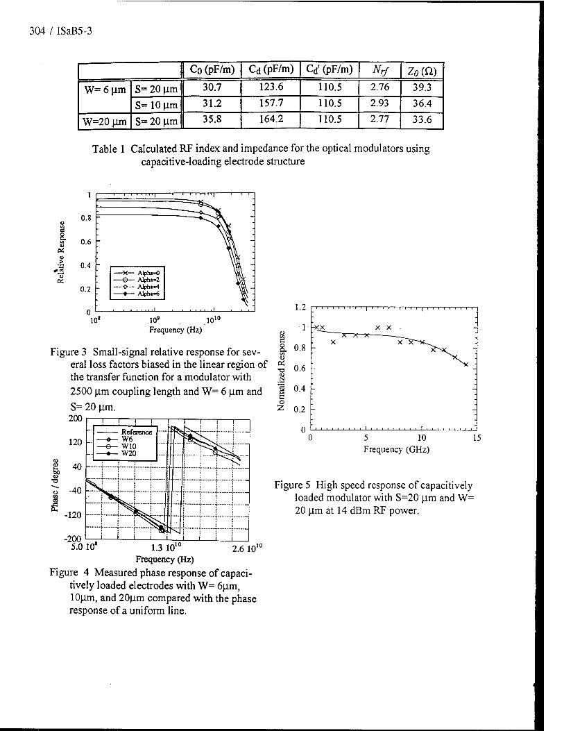
304 / ISaB5-3
Co (pF/m) Cd (pF/m) Cd' (pF/m) AV Zo(n>
W=6nm S= 20 urn 30.7 123.6 110.5 2.76 39.3
S= 10 u.m 31.2 157.7 110.5 2.93 36.4
W=20 |im S= 20 |im 35.8 164.2 110.5 2.77 33.6
Table 1 Calculated RF index and impedance for the optical modulators using capacitive-loading electrode structure
a
u
0.8
0.6
0.4
0.2 -
Aiph»=0 Alpha-2 A%>hi»4 Alpha-6
108 109
Frequency (Hz) 10 10
Figure 3 Small-signal relative response for sev- eral loss factors biased in the linear region of the transfer function for a modulator with 2500 (im coupling length and W= 6 |im and
S= 20 urn.
I
200
-200 5.0 108
2.6 10 1.3 10 Frequency (Hz)
Figure 4 Measured phase response of capaci- tively loaded electrodes with W= 6}im, lOjim, and 20|im compared with the phase response of a uniform line.
10
T3
a
o 2
5 10 Frequency (GHz)
15
Figure 5 High speed response of capacitively loaded modulator with S=20 fim and VV= 20 u.m at 14 dBm RF power.
ISaC 1:30 pm-3:00 pm Salon 1
Mark L. Lowry, Presider Lawrence Livermore National Laboratory
Saturday, February 25, 1995
Array Technologies and Applications

306 / ISaCl-1
Optoelectronics Packaging and Passive Fiber Optic Array Attachment
Robert A. Boudreau, Hongtao Han, Ping Zhou, W. X. Zou, and Terry Bowen
AMP Incorporated M/S 140-58, P.O. Box 3608 Harrisburg, PA 17105 -3608
Phone: (717) 986-5904, Fax: (717)-986-5071, Internet: [email protected]
Background - It now appears certain that fiber optic arrays will soon be an important interconnect component. Applications will include array interconnects for SONET transport systems, cross-connect switches, parallel interconnects in multi-processor computers, and ATM switches. Currently, many of these products use an awkward assortment of heavy coaxial cables that are terminated with D-connectors similar to those on the back of our desk top computers. Space restrictions, reliability issues related to multi-racks of heavy connectors, and limitations in performance are making optical interconnects appear as an attractive alternative. In addition, new technologies and an emphasis on design for cost reduction has made array optical interconnections more attractive. Once optical interconnect becomes equivalent to the cost of electrical interconnect there will be a dramatic increase in its application and further cost reduction.
Arrays present a special opportunity for dramatic cost reductions per channel depending on the method of packaging. Traditional optoelectronic packaging, where individual fibers are aligned by peaking an optical signal in a process know as active alignment, may not be the best approach. The optical alignment is the most costly part of an actively aligned component and there is little room for the fixturing required for closely spaced array members. A gang alignment where the optical signal strength is peaked for the two outside members of the array is better, but still difficult. The best solution, if possible, is to use a passive alignment approach. Passive alignment is where the optical components are aligned to the optical fiber or waveguides without having to operate the device. Parts either "snap" together as a result of some physical or mechanical feature, or they are aligned to optical alignment marks. If a passive alignment approach is used the cost for the alignment of the array device may be nearly the same as for a single laser device.
The difficulty in packaging an optical interconnect by passive alignment depends on whether the optical interconnect is single-mode or multi-mode. For high speed applications single- mode interconnects offer the advantage of less optical noise. Also, single mode fiber is less expensive than multi-mode fiber. Unfortunately, however, the mechanical positional tolerance of single mode optical alignments is roughly an order of magnitude worse than that for multimode. Telecom tends to use single-mode optical links with long wavelength light sources while datacom tends to use multi-mode fiber with short wavelength light sources. This situation is driven by cost at the expense of unneeded performance. If single-mode alignments become nearly equivalent in cost to multi-mode alignments it is likely that more and more of the industry will shift to single-mode. This paper will focus predominantly on methods for single- mode because the multi-mode optical alignment is much less difficult.
Passive Alignment - There are several types of passive alignment systems depending on the types of arrays to be aligned. If it is a connector, the MT style array connector1 currently
Developed by Alcoa Fujikura, now offered by U.S. Conec
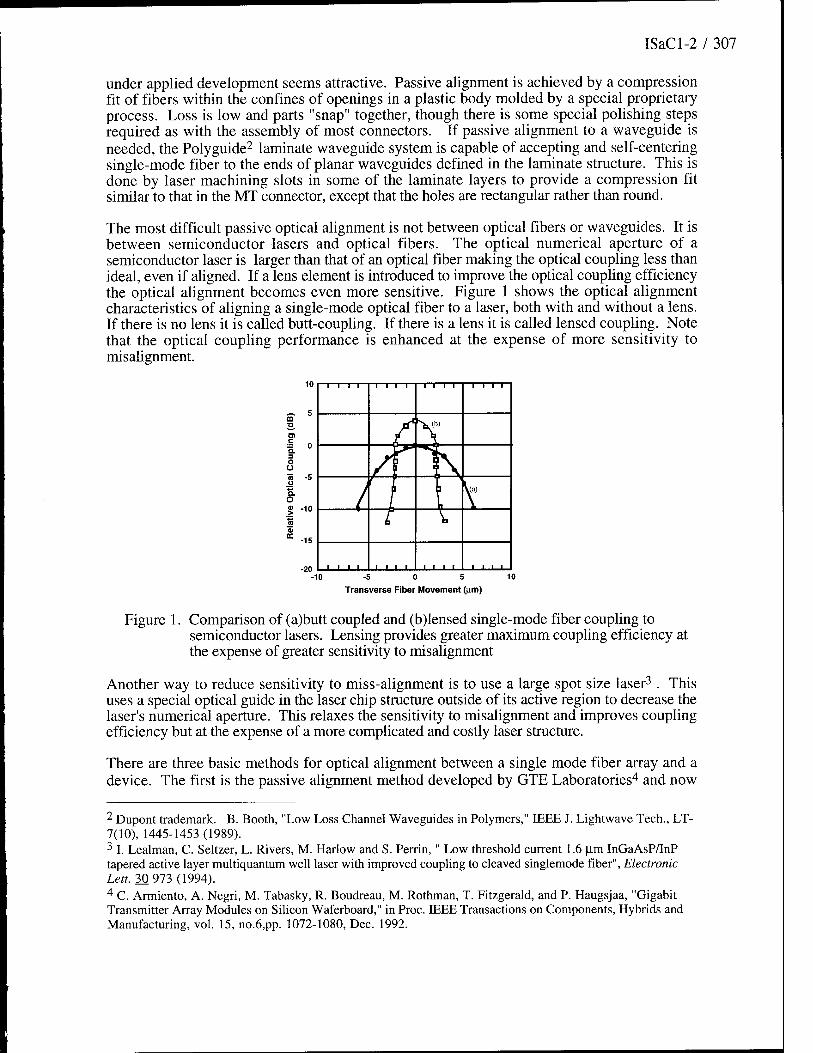
ISaCl-2 / 307
under applied development seems attractive. Passive alignment is achieved by a compression fit of fibers within the confines of openings in a plastic body molded by a special proprietary process. Loss is low and parts "snap" together, though there is some special polishing steps required as with the assembly of most connectors. If passive alignment to a waveguide is needed, the Polyguide2 laminate waveguide system is capable of accepting and self-centering single-mode fiber to the ends of planar waveguides defined in the laminate structure. This is done by laser machining slots in some of the laminate layers to provide a compression fit similar to that in the MT connector, except that the holes are rectangular rather than round.
The most difficult passive optical alignment is not between optical fibers or waveguides. It is between semiconductor lasers and optical fibers. The optical numerical aperture of a semiconductor laser is larger than that of an optical fiber making the optical coupling less than ideal, even if aligned. If a lens element is introduced to improve the optical coupling efficiency the optical alignment becomes even more sensitive. Figure 1 shows the optical alignment characteristics of aligning a single-mode optical fiber to a laser, both with and without a lens. If there is no lens it is called butt-coupling. If there is a lens it is called lensed coupling. Note that the optical coupling performance is enhanced at the expense of more sensitivity to misalignment.
= o
1 1 1 1 1 1 1 1 ■ i i i
^fa»)
X i i
V«
1 1 1 1 -till 1 1 1 1 -5 0 5
Transverse Fiber Movement (^m) 10
Figure 1. Comparison of (a)butt coupled and (b)lensed single-mode fiber coupling to semiconductor lasers. Lensing provides greater maximum coupling efficiency at the expense of greater sensitivity to misalignment
Another way to reduce sensitivity to miss-alignment is to use a large spot size laser3 . This uses a special optical guide in the laser chip structure outside of its active region to decrease the laser's numerical aperture. This relaxes the sensitivity to misalignment and improves coupling efficiency but at the expense of a more complicated and costly laser structure.
There are three basic methods for optical alignment between a single mode fiber array and a device. The first is the passive alignment method developed by GTE Laboratories4 and now
2 Dupont trademark. B. Booth, "Low Loss Channel Waveguides in Polymers," IEEE J. Lightwave Tech., LT- 7(10), 1445-1453 (1989). 3 I. Lealman, C. Seltzer, L. Rivers, M. Harlow and S. Perrin," Low threshold current 1.6 |i.m InGaAsP/InP tapered active layer multiquantum well laser with improved coupling to cleaved singlemode fiber", Electronic Lett. 30 973(1994). 4 C. Armiento, A. Negri, M. Tabasky, R. Boudreau, M. Rothman, T. Fitzgerald, and P. Haugsjaa, "Gigabit Transmitter Array Modules on Silicon Waferboard," in Proc. IEEE Transactions on Components, Hybrids and Manufacturing, vol. 15, no.6,pp. 1072-1080, Dec. 1992.
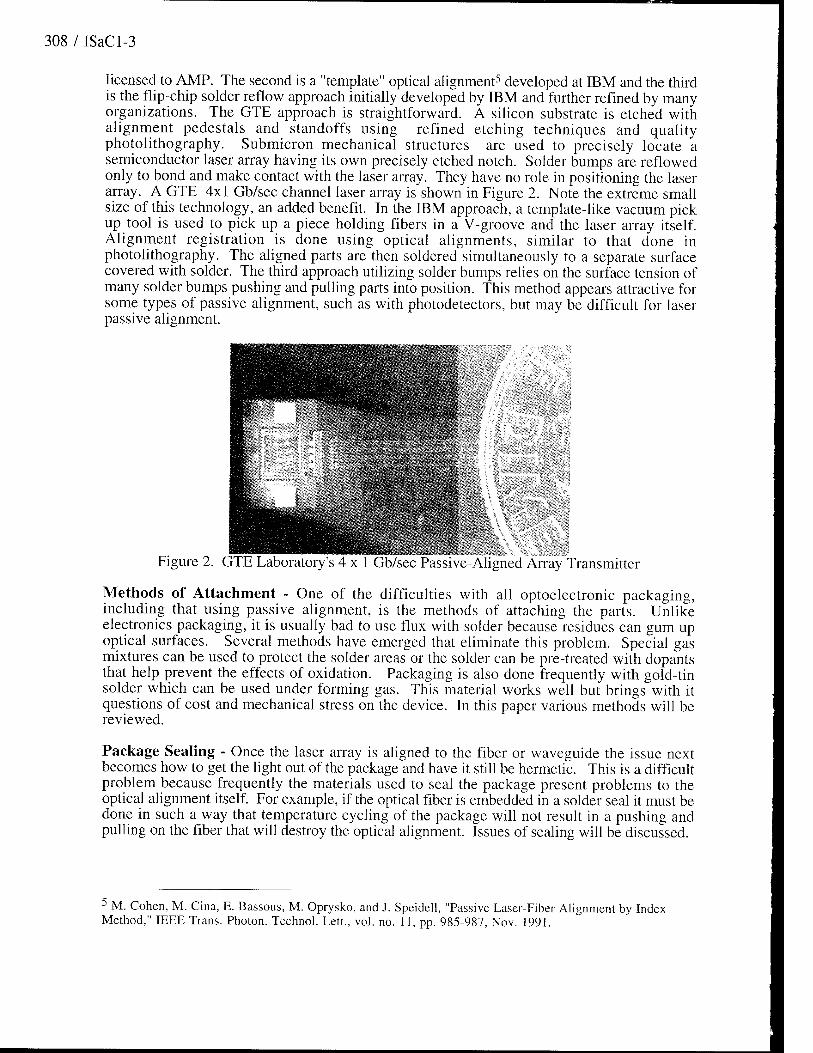
308 / ISaCl-3
licensed to AMP. The second is a "template" optical alignment5 developed at IBM and the third is the flip-chip solder reflow approach initially developed by IBM and further refined by many organizations. The GTE approach is straightforward. A silicon substrate is etched with alignment pedestals and standoffs using refined etching techniques and quality photolithography. Submicron mechanical structures are used to precisely locate a semiconductor laser array having its own precisely etched notch. Solder bumps are reflowed only to bond and make contact with the laser array. They have no role in positioning the laser array. A GTE 4x1 Gb/sec channel laser array is shown in Figure 2. Note the extreme small size of this technology, an added benefit. In the IBM approach, a template-like vacuum pick up tool is used to pick up a piece holding fibers in a V-groove and the laser array itself. Alignment registration is done using optical alignments, similar to that done in photolithography. The aligned parts are then soldered simultaneously to a separate surface covered with solder. The third approach utilizing solder bumps relies on the surface tension of many solder bumps pushing and pulling parts into position. This method appears attractive for some types of passive alignment, such as with photodetectors, but may be difficult for laser passive alignment.
Figure 2. GTE Laboratory's 4 x 1 Gb/sec Passive-Aligned Array Transmitter
Methods of Attachment - One of the difficulties with all optoelectronic packaging, including that using passive alignment, is the methods of attaching the parts. Unlike electronics packaging, it is usually bad to use flux with solder because residues can gum up optical surfaces. Several methods have emerged that eliminate this problem. Special gas mixtures can be used to protect the solder areas or the solder can be pre-treated with dopants that help prevent the effects of oxidation. Packaging is also done frequently with gold-tin solder which can be used under forming gas. This material works well but brings with it questions of cost and mechanical stress on the device. In this paper various methods will be reviewed.
Package Sealing - Once the laser array is aligned to the fiber or waveguide the issue next becomes how to get the light out of the package and have it still be hermetic. This is a difficult problem because frequently the materials used to seal the package present problems to the optical alignment itself. For example, if the optical fiber is embedded in a solder seal it must be done in such a way that temperature cycling of the package will not result in a pushing and pulling on the fiber that will destroy the optical alignment. Issues of sealing will be discussed.
5 M. Cohen, M. Cina, E. Bassous, M. Oprysko, and J. Speidell, "Passive Laser-Fiber Alignment by Index Method," IEEE Trans. Photon. Technol. Lett., vol. no. 11, pp. 985-987, Nov. 1991.
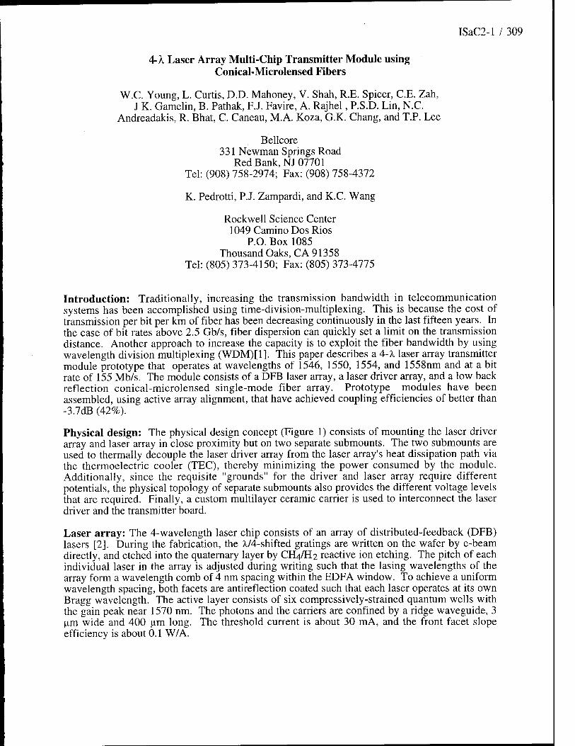
ISaC2-l / 309
4-A, Laser Array Multi-Chip Transmitter Module using Conical-Microlensed Fibers
W.C. Young, L. Curtis, D.D. Mahoney, V. Shah, R.E. Spicer, C.E. Zah, J K. Gamelin, B. Pathak, FJ. Favire, A. Rajhel, P.S.D. Lin, N.C.
Andreadakis, R. Bhat, C. Caneau, M.A. Koza, G.K. Chang, and T.P. Lee
Bellcore 331 Newman Springs Road
Red Bank, NJ 07701 Tel: (908) 758-2974; Fax: (908) 758-4372
K. Pedrotti, P.J. Zampardi, and K.C. Wang
Rockwell Science Center 1049 Camino Dos Rios
P.O. Box 1085 Thousand Oaks, CA 91358
Tel: (805) 373-4150; Fax: (805) 373-4775
Introduction: Traditionally, increasing the transmission bandwidth in telecommunication systems has been accomplished using time-division-multiplexing. This is because the cost of transmission per bit per km of fiber has been decreasing continuously in the last fifteen years. In the case of bit rates above 2.5 Gb/s, fiber dispersion can quickly set a limit on the transmission distance. Another approach to increase the capacity is to exploit the fiber bandwidth by using wavelength division multiplexing (WDM)[1]. This paper describes a 4-X laser array transmitter module prototype that operates at wavelengths of 1546, 1550, 1554, and 1558nm and at a bit rate of 155 Mb/s. The module consists of a DFB laser array, a laser driver array, and a low back reflection conical-microlensed single-mode fiber array. Prototype modules have been assembled, using active array alignment, that have achieved coupling efficiencies of better than -3.7dB (42%).
Physical design: The physical design concept (Figure 1) consists of mounting the laser driver array and laser array in close proximity but on two separate submounts. The two submounts are used to thermally decouple the laser driver array from the laser array's heat dissipation path via the thermoelectric cooler (TEC), thereby minimizing the power consumed by the module. Additionally, since the requisite "grounds" for the driver and laser array require different potentials, the physical topology of separate submounts also provides the different voltage levels that are required. Finally, a custom multilayer ceramic carrier is used to interconnect the laser driver and the transmitter board.
Laser array: The 4-wavelength laser chip consists of an array of distributed-feedback (DFB) lasers [2]. During the fabrication, the ^/4-shifted gratings are written on the wafer by e-beam directly, and etched into the quaternary layer by CH4/H2 reactive ion etching. The pitch of each individual laser in the array is adjusted during writing such that the lasing wavelengths of the array form a wavelength comb of 4 nm spacing within the EDFA window. To achieve a uniform wavelength spacing, both facets are antireflection coated such that each laser operates at its own Bragg wavelength. The active layer consists of six compressively-strained quantum wells with the gain peak near 1570 nm. The photons and the carriers are confined by a ridge waveguide, 3 [im wide and 400 (im long. The threshold current is about 30 mA, and the front facet slope efficiency is about 0.1 W/A.

310/ISaC2-2
Optical coupling: In view of the submicron type alignments that are required for sufficient coupling efficiency between a laser and a single-mode fiber, it was decided to use an active alignment scheme to achieve similar efficiencies with array lasers. Furthermore, to simplify the physical design of the module, a low-reflectance conical-microlensed fiber tip [3] was selected for butt-coupling to the laser array. These conical microlensed fibers have been shown to achieve coupling efficiencies of 50% with back reflections of less than -55dB. In cases where additional optical isolation is required, an inline isolator can be added after the wavelengths are combined into a single fiber. Finally, the array alignment is made with a micro-manipulator having five degrees of freedom.
Fiber array: Preferentially-etched silicon v-grooves were used to fabricate the fiber arrays. The fibers used in the array fabrication were selected for their precise geometrical properties such as precise outside diameter, concentric core/cladding, and well centered conical microlenses. The fibers were assembled in the silicon substrates such that the lensed fiber tips were slightly protruding and coplanar. After assembly, the fiber arrays were fully dimensionally characterized.
Thermal management: The thermal analysis of the module was completed by using a combination of analytical techniques and finite element modeling. In this work, we considered numerous parameters including IC power dissipation levels, the effect of the TEC cold side temperature, the ambient temperature effects, and also the effect of insulation, i.e., varying film coefficients. As mentioned above, the driver array is thermally isolated from the laser array and only the laser array's temperature is controlled by the TEC. On the other hand, the driver array is cooled via a heat spreader and heat sink, and as a result, the driver's temperature is a strong function of the local ambient temperature. The analyses show that the maximum temperature of the driver array is about 18°C above the local ambient's temperature. With regards to the lasers, their temperature is determined by the temperature boundary condition imposed by the TE cooler. In this case, the maximum laser temperature is about 7°C above the TEC's cold side. The analysis also shows a variation in laser temperature as a function of location in the array. For the case of four lasers, spaced 500 microns apart, the maximum temperature difference is 0.7°C.
Driver array: The laser driver array is implemented with AlGaAs/GaAs heterojunction bipolar transistors. The peak current delivered to each laser is 60 mA, of this up to 30 mA can be a DC bias current with the modulation current adjustable up to 30 mA peak-to-peak. The circuit is designed for an input signal of 300 mV differential into 50 ohms. The modulation currents are separately adjustable for each channel and an additional pad and resistor are supplied for each channel to allow for small bias current adjustments to compensate for any laser threshold variations. The circuit uses a differential signal path to achieve good common mode rejection to reduce crosstalk. The drivers were fabricated on a 500 pm spacing to match the DFB laser spacing, and care was taken to minimize capacitive coupling and crosstalk between the channels.
Ceramic carrier: A custom six-layer ceramic carrier provides fanout circuits between the laser driver array and the 78 external solder tabs that are arranged in a butterfly package configuration. Some of the characteristics of the ceramic carrier are (a) the 78 I/O pads are on a 25 mil pitch, (b) a ribbon lead-frame is brazed to the I/O pads, and (c) a two-tier wirebond pad topology (featuring 4 mil pitch, 2 mil wide bond pads) is utilized. In addition, the carrier features seven metallization layers, six ceramic layers, 50 ohm conductors for the high-speed differential signals, and a layer that facilitates the mounting of decoupling capacitors.
Results: A 4-X laser array transmitter module has been designed and fabricated using a butt- coupled conical-microlensed single-mode fiber array, and an active alignment method was developed for aligning the laser and fiber array. Optimum coupling efficiencies were achieved
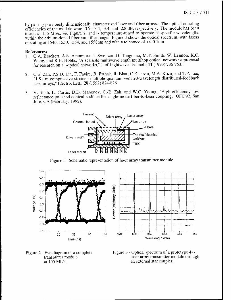
ISaC2-3 / 311
by pairing previously dimensionally characterized laser and fiber arrays. The optical coupling efficiencies of the module were -3.7, -3.4, -3.4, and -2.8 dB, respectively. The module has been tested at 155 Mb/s, see Figure 2, and is temperature-tuned to operate at specific wavelengths within the erbium-doped fiber amplifier range. Figure 3 shows the optical spectrum, with lasers operating at 1546, 1550, 1554, and 1558nm and with a tolerance of+/- 0.1 nm.
References: 1. C.A. Brackett, A.S. Acampora, J. Sweitzer, G. Tangonan, M.T. Smith, W. Lennon, K.C.
Wang, and R.H. Hobbs, "A scalable multiwavelength multihop optical network: a proposal for research on all-optical networks," J. of Lightwave Technol., 11 (1993) 736-753.
2. C.E. Zah, P.S.D. Lin, F. Favire, B. Pathak, R. Bhat, C. Caneau, M.A. Koza, and T.P. Lee, "1.5 u.m compressive-strained multiple-quantum-well 20-wavelength distributed-feedback laser arrays," Electro. Lett., 28 (1992) 824-826.
3. V. Shah, L. Curtis, D.D. Mahoney, C.-E. Zah, and W.C. Young, "High-efficiency low reflectance polished conical endface for single-mode fiber-to-laser coupling," OFC'92, San Jose, CA (February, 1992).
Housing Dr|ver array y Laser array
Ceramic fanout /\
Driver mount
Fiber array
5*fan ^ Fibers
Thermal/electrical isolators
TEC
Laser mount
Figure 1 - Schematic representation of laser array transmitter module.
c
CO
CD
o CL
1542
^~ J U| ■AA/ W A/J kJU r\/\f
■■ i— 1546 1550 1554
Wavelength (nm) 1558 62
Figure 2 - Eye diagram of a complete transmitter module at 155 Mb/s.
Figure 3 - Optical spectrum of a prototype 4-A, laser array transmitter module through an external star coupler.
312 / ISaC3-l
Integrated Microlens Array for Optical Interconnects
O. Blum, S. Kilcoyne, M. E. Warren, R. F. Carson, T. Du Sandia National Laboratories, Dept. 1312, MS0603, P.O. Box 5800, Albuquerque, NM 87185-
0603, Phone (505) 844-3458, Fax (505) 844-8985 G. Robinson
Optical Concepts Inc., P.O. Box 668, Lompoc, CA 93438-0668, Phone (805) 737-7391, Fax (805) 737-7393
As Multi-Chip Modules (MCMs) grow in chip count and complexity, increasingly large numbers of Input/Output (I/O) channels will be required for connection to other MCMs or printed wiring boards. In applications such as digital signal processing, large increases in processing density (number of operations in a given volume) can be obtained in stacked MCM arrangements. The potential pin counts and required I/O densities in these stacked architectures will require technology beyond the limits of present day capabilities. This problem is particularly acute if easy separation of layers is needed to meet MCM testing and yield requirements. One solution to this problem is the use of optoelectronic data channels that operate in large arrays [1]. These arrays will emit and detect signals traveling normal to the surface of the MCM stack as in Fig. 1. In order to maximize compatibility with present MCM packaging techniques, the chips that form the arrays should include both the active devices (sources such as vertical cavity surface emitting lasers (VCSELs) and detectors as shown in the demonstration cross-section in Fig. 2) and any collimation and/or focusing optics that are needed to compensate for misalignments and accommodate small detector areas. This provides a strong motivation for the integration of refractive microlenses directly onto photonic device chips. In addition, integrated microlenses are of great utility in facilitatitng board-to-board interconnects, as well as fiber coupling of VCSELs. In this summary we describe a simple and manufacturable process for fabrication of such microlens arrays and report on their performance. Several different processes have been attempted for lens integration, including monomer exchange in plastics, electromigration, ion exchange, photoresist reflow and others [2]. In most cases these lenses are not compatible with integration with active III-V devices such as surface emitting lasers due to processing requirements, thermal stability or performance. We describe the fabrication and performance of integratible microlenses varying in size from 5 )i m to 50 f^m fabricated using a polyimide compound and lithographic techniques suitable to fabrication on the backside of the active device substrate. First, a 3 (im thickness of polyimide was spun onto the surface and baked out. Then conventional photoresist was spun on top and circles of the desired diameter for the lenses were lithographically defined. The polymide layer was then deep UV exposed using the photoresist circles as a mask and subsequently developed. A small thickness of the underlying GaAs substrate (0.6|im) was then dry etched everywhere except where it was masked by the polyimide and photoresist circle. In this way a small GaAs step was created under the polyimide circle. Photoresist was then removed and a 3 fim polyimide disk reflowed on a hot plate (300°C for 5 minutes). It should be noted that the polyimide starts reflowing at much higher temperatures than photoresist (185°C vs. 100°C), ensuring greater thermal stability of the microlenses. The edge of the GaAs pedestal prevents the polyimide from flowing freely. A spherical surface is thus formed with a radius of curvature determined by the disk diameter and initial thickness of the polyimide film. We have investigated this dependence

ISaC3-2 / 313
by fabricating lenses of 5 |im to 50 (im diameters and measuring their focal lengths at 980 nm wavelength. In order to accomplish this we used a spatially filtered and collimated Ti:Sapphire laser incident on the clear side of a polished GaAs wafer and focused by a polyimide lens integrated on the other side of the wafer. A microscope objective placed on the microlens side of the GaAs substrate was used to first image the lens onto a CCD camera and then to focus the laser light coming through it. The difference between the positions of the microscope objective necessary to obtain these two images was taken to be the focal length of the microlens. The results of this experiment are summarized in the table below:
Diameter 50|im 30[im 20|im 15 |im 12(im lOfim 8|im 5(im
Focal length
100 pi m
36(im 26(im 16[im llfxm 10.5H
m 8|im 2.5[im
N.A. 0.25 0.42 0.38 0.47 0.55 0.48 0.5 1.0
Scanning electron micrographs of the 5 |im and a 50 |im microlenses are shown in Fig. 3a and Fig. 3b respectively. The 5 (im lens has a nearly hemispherical profile, which accounts for the very high numerical aperture (N.A.) observed for that lens size. The 50 |im lens is considerably flatter, but its focal length (100 |im) is sufficient for integration with a vertical cavity surface emitting laser (VCSEL) fabricated on the other side of the 350 |im GaAs substrate and designed to emit through its bottom mirror. Despite small divergence angle for VCSEL devices (10°), in a typical device with an 8 ^im waist, the beam spreads to 167 |im after propagating through 350 |im of the substrate and 850 ^.m of free space. By integrating a microlens with 100 |im focal length on the backside of the substrate, 850 Jim away the beams size is reduced to 60 |im. This ability to approximately collimate has considerable impact on design and alignment of the next layer of photonic devices in our MCM application. Another area of improvement offered by integration of microlenses directly onto optoelectronic devices is detector performance. Not only can responsivity be improved by ensuring a larger effective collection angle, but the device speed also benefits as a result of the reduced detector area which results in reduced capacitance. Microlenses also allow for greater system design flexibility. By depositing metal on the backside of the substrate over the microlenses and using them in reflection, Cassegrain configurations can be implemented, thus allowing for enhanced collection when light is incident on the top of the detector chip. We have also transfered the microlenses into GaAs substrate, using the polyimide microlens itself as a mask and employing electron cyclotron resonance (ECR) etching. Faster lenses are obtained by this approach, because of the faster etch rate of GaAs and greater refractive index (3.5 vs. 1.5). The 50 |im microlens with a 100 |im focal length in polyimide, became a 42 (im diameter lens with a focal length of 18 (im upon transferring it into GaAs substrate. It's N.A. drastically increased from 0.25 to 0.85. SEM examination of the lens revealed very smooth morphology and no distortions were observed when the light was focused. All semiconductor lenses are advantageous, because of better thermal and mechanical stability. In conclusion, we have demonstrated microlenses fabricated by a simple, manufacturable process with diameters and focal lengths compatible for integration with a variety of active photonic devices. Such microlenses are vital components in optical technologies, such as MCM stacks for digital signal processing, board-to-board interconnects and fiber coupling.
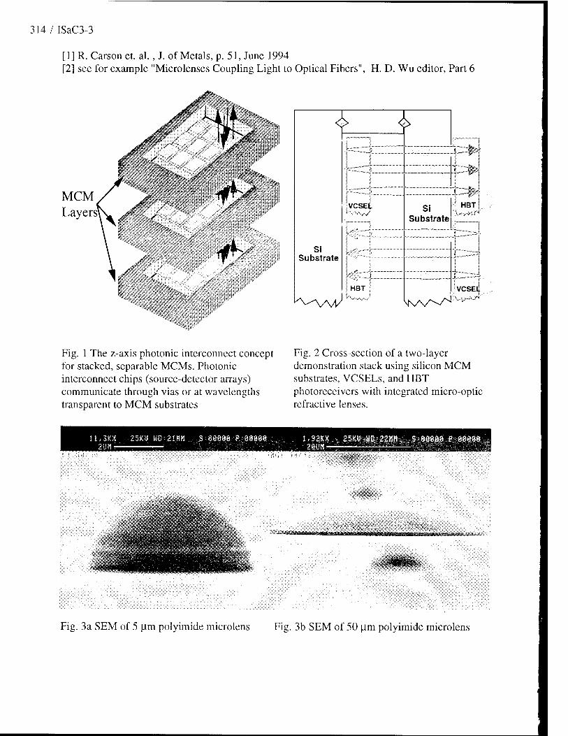
314 / ISaC3-3
[1] R. Carson et. al., J. of Metals, p. 51, June 1994 [2] see for example "Microlenses Coupling Light to Optical Fibers", H. D. Wu editor, Part 6
MCM Layers1
•
/
•'■■'■■' A
tUUUnv
9 mmnir
4^
5 I
Si Substrate
■vW
jVCSEt
„..A~
\ HBT i
~r~~~#te.
Si Substrate
':M
' HBT j
VCSEI
Wv^
Fig. 1 The z-axis photonic interconnect concept for stacked, separable MCMs. Photonic interconnect chips (source-detector arrays) communicate through vias or at wavelengths transparent to MCM substrates
Fig. 2 Cross-section of a two-layer demonstration stack using silicon MCM substrates, VCSELs, and HBT photoreceivers with integrated micro-optic refractive lenses.
U3KK 25t«J «K21MN 2UH '" ' ' ■
.S:ft8W8 £.-' 88898 i,32KX - 25K« m--22m. 5 = 88898 1^80880
w%$&Mä^'
Fig. 3a SEM of 5 p.m polyimide microlens Fig. 3b SEM of 50 |im polyimide microlens

ISaC4-l / 315
Parallel Optical Interconnects for Computing—A Potential High-Volume Market
David K. Lewis Martin Marietta Laboratories-Syracuse P.O. Box 4840, Syracuse, NY 13221
Summary not available.

316 / NOTES

Key to Authors and Presiders / 317
Ackerley, N. — IThF2 Doran, N. J. — IFD4 Jiang, P. — IFE2
Ade, R. W. — IFE4 Dragone, C. — ISaA1 Johnson, Klein L. — IFF2
Ahlers, E. — IThB3 Du, T — ISaC3 Judkins, Justin B. — IThF4
Aitchison, J. S. — IThC22 Duchet, C — IThG24
Akahori, Yuji — IThA1, IThA4 Kadota, Yoshiaki — IFA2
Akatsu, Yuji — ITHA1, IThA4 Elwood, Persis A. — IThE4 Kar-Roy, A. — IThGI 5
Alferness, R. C. — L2 Emanuel, M. A. — IThC4, IThG11 Karpov, V. 1. — IFC3
Andreadakis, N. C. — lSaC2 Katoh, Yujiro — IThCI
Arney, S. C. — ISaA6 Farwell, Mark L. — IThF5 Kawahara, M. — IThG20, ISaB3
Favire, F. J. — ISac2 Kearley, M. Q. — IFE1
Baek, J. H. — IThG17 Fischbeck, Goetz — IThC3 Kendall, P.C. —IThG5
Baets, R. — IThG6 Fischer, Uwe — IThC2 Khan, M. N. — IThD4, ISaA3
BaranJaneE. — IFD5 Forrest, S. R. — IFA5 Khrapko, R. R. — IFC3
Bebbington, J. A. — IThG22 Bennion, 1. — IFD4
Freking, Robert—IThD2 Kilcoyne, S. — ISaC2
Fritz, I. J. —IThGI 8 Koch, T. L. — IThD5
Berry, G.M. —IThGIO Bhat, R. — ISaC2
Froberg, N. M. — ISaA1 Koren, U. — ISaA1 Kornacki, K. P. — IFE4
Birks, T. A. — IThG2 Gamelin, J. K. — ISaC2 Korotky, Steve — Plenary 1, 2
Bishop, S. G. — IThG21 Garbuzov, D. — IFA5 Koza, M. A. — ISaC2
Bjarklev, Anders — IThGI, IThG12 Gelly, G. — ISaA4 Kozen, A. — IThA1
Blum, Olga —IThG18 Glynn, G. — IFE1 Kurkov, A. S. — IFC3
Bogatyrjov, V. A. — IFC3 Goel, K. K. — IThGI 3 Kwon, O. K. — IThGI 7
Bonar, J. R. — IThG22 Golant, K. M. — IFC3
Bossi, Donald E. — IThEl Goodwin, M. J. — IFE1 Laborde, Pascale — IFC4
Boudreau, Robert A. — ISaCI Goorjian, Peter M. — IThFI Lagasse, Paul — L3
Bowen, Terry — ISaCI Goossen, K. W. — ISaA6 Langley, L. N. — IThG4
Bowers, John E. — IFA1 Gopinath, Anand — IThD2, IFB2, IFF2, Larson, M. C. — IThGI 6
Bristow, Julian — IFF2 ISaB5 Le Du, F. — ISaA4
Brot, C. — IThG24 Greenblatt, A. S. — IFE3 Lee, B. —IThGI 7
Bulmer, C. H. — IFE3 Groen, Fokke H. — IThG23 Lee, E.-H. — IThGI 7
Burke, S.V.— IThGIO Gu, S. Q. — IThG21 Lee, Hyung-Jae — IThG25
Burns, W. K. — IFE3 Lee, T P. — ISaC2
Burrus, C. A. — ISaA1, ISaA2 Hadley, G. Ronald — IThB, IFB1 Lerminiaux, Christian — IFC4
Burton, R. R. — IThG5 Haes, J. — IThG6 Lester, Christian — IThGI, IThGI2
HallJ. P. — IFE1 Lewis, David K. — ISaC4
Camy, Patrice — IFC4 Han, Hongtao — ISaCI Li, G. P. — IFA4
Caneau, C. — ISaC2 Hanatani, S. — IThA2 Li, X. — IThG7
Carson, R. F. — ISaC3 Harris, James S., Jr. — IThGI 6 Lin, P. S. D. — ISaC2
Chang, G. K. — IFD5, ISaC2 Hasegawa, Akira — L1 Liu, Yue—IFF2
Chang, Hung-Chun — IThG3 Chang, Milton — L4 Chang, T.-Y. — ISaA2
HeatonJ.M. —IThGIO Lloyd-Lucas, F. D. — IThG2
Heismann, F. — ISaB2 Lowry, Mark — IThE2, IThE3, ISaC2
Helfen, S. — IThB5 Lu, ShinYee—IThE2, IThE3
Chang, William S. C. — IThF5 Hempstead, Martin — IFC4
Chao, C.-P. — IFA5 Hibino, Y. — IThC6 Ma, F. — IThG8, IThGI 4
Chaudhuri, S. K. — IThF2, IFD Hida, Y. — IThC6 Mahoney, D. D. — ISaC2
Chien, M. — ISaA1 Hornung, V. — ISaA4 Makino, T — IThG7, IFA4
Chinni, V. R. — IFB4 Howard, A. J. —IThGI 8 Maring, David B. — IThC5
Choi, Y. W. — IThGI 7 Huang, Chi-Hung — IFC2 McBrien, G. J. — IFE4
Chowdhury, Dipakbin Q. — IFF5 Huang, W. P. — IThG7, IThG8, McCaughan, Leon — IFC2, ISaB
Croston, Ian R. — ISaC IThGI 4, IFA4 Menyuk, C. R. — IFB4
Curtis, L. — ISaC2 Ido, Tatemi — !SaA5 Mertens, K. — IFB5
llic, Igor—IThG9 Metaal, Ed G. — IThG23
Dagli, Nadir—IThD, IFB3 Inoue, Hiroaki — !SaA5 Mihailidi, M. M. — !ThD4
Deri, R. J. — IThC4, IThG11, IFA, IFA3 Iqbal, M. Z. — IFD5 Miller, B. 1. — ISaA1
DiMaggio, M. — IThG24 Islam, Mohammed N. — Plenary 1 Moeller, R. P. — IFE3
Dianov, E. M. — IFC3 Itaya, Yoshio — IThA1, IThA4 Moerman, Ingrid — IThG23
Dijaili, S. P. — IThC4, IFA3 Mori, Hidefumi — IFA2
Dinesen, P. G. — IThGI, IThGI 2 Jackel, Janet L. — IFD5, ISaB4 Moseley, A. J. — IFE1
Dodson, J. — IFE2 Jensen, Per Inge — IThB4 Muramoto, Y. — IThA1

318/ Key to Authors and Presiders
Nagarajan, Radhakrishnan — IThDI Nagata, Hirotoshi — ISaBI Nakamura, H. —IThA2 Nakano, Hisamatsu — IThB2 Nayyer, Jamshid — ISaBI Nolan, Daniel A. — IFF5
O'Donnell, A. — IFE2 Oei, Y. Siang —IThC23 Ohmori, Y. — IThC6 Okayama, H. — IThG20, ISaB3 Okazaki, H. — IThC6 Osgood, Richard M., Jr. — IThG9 Ouellette, F. — IThG13
Pan, X. — IThD5 Pathak, B. — ISaC2 Patterson, F. G. — IThC4, IFA3 Pechstedt, R. D. — IThG2 Pedersen, Jörgen W. — IThG23 Pedrotti, K. — ISaC2 Petermann, Klaus — IThC2, IThC3 Pezeshki, B. — IThG16 Pocha, Michael — IThE3 Pohl, M. — IThF3 Pregla, Reinhold — IThB3, IThB5, IThF,
IFD1 Protopopov, V. N. — IFC3
Rajhel, A. — ISaC2 Ramachandran, S. — IThG21 Ramanujan, Sujatha — IFF1 Ramaswamy, Ramu V. — IThCS Rangwala, Sabbir— IFE5 Rasmussen, Thomas — IThGI, IThG12 Rawsthorne, J. R. — IFE1 Raybon, G. — ISaA1, ISaA2 Reuter, E. E. — IThG21 Reynolds, C. — IFE2 Ripoche, G. — ISaA4 Robinson, G. D. — ISaC3 Robson, P. N.— IThG5 Rodino, V. D. — IFE4 Rolland, Claude— ISaA Roman, Jose E. — IFC4 Rossmann, M. L. — IFD2 Russell, P. St. J. — IThG2
Sano, Hirohisa — IThA2, ISaA5 Sarangan, A. M. — IThG8, IFA4 Sasaki, Tohru — IFA2 Sauer, N.J. —ISaA2 Scarmozzino, Robert — IThG9 Schmitt, H.J. —IFB5 Schneider, R. P., Jr. — IThGI 8 Scholl, B. — IFB5 Schulman, J. N. — IFD3 Schulz, D. —IThF3, IFD2 Seki, Shunji — IFF3 Sennewald, M. — IFB5 Shah, V. — ISaC2
Shiau, G.-J. — IFA5 Shibayama, Jun — IThB2 Shin, Sang-Yung — IThG25 Shishikura, M. — IThA2 Shore, K. A. — IThD3, IThG4 Silberberg, Yaron — IThFI Sivasubramaniam, S. Y. — IFB4 Smith, David A. — ISaB4 Smith, R. Kent—IFB6 Sohler, W. — IFC1 Song, G. Hugh — IFD5 Sood, Deepak — IThE2 Soole, Julian B. — IThC Stakelon, Thomas — IFE5 Stern, M. S. — IThG5, IThGI4 Strand, Oliver T. — IThE2, IThE3 Sudbo, Aasmund — IThB4 Sugimoto, Naoto — IThC1 Sun, B. — IThG15
Tachikawa, Masami — IFA2 Takahata, K. — IThAI Tanaka, Shigehisa — IThA2, ISaA5 Täte, Akiyuki — IThCI Tavlykaev, Robert F. — IThC5 Tokuda, K. L. — ISaB2 Tomlinson, W. Jack — IThE, IFD5 Tsai, C. S. — IThGI 5 Tsuji, S. — IThA2 Turnbull, D. A. — IThG21 Turovets, S. I. — IThG4
van der Tol, Jos J.G.M. — IThG23 Verbeek, Bart H. — IThA3 Verdeyen, J. T — IThG21 Vinchant, J.- F. — ISaA4 Voges, E. — IThF3, IFD2 Voisine, K. R. — IFE4
Wai, P. K. A. — IFB4 Wakita, Koichi — ISaA3 Walker, J. A. — ISaA6 Wang, K. C. — ISaC2 Warren, M. E. — ISaC3 Weidman, David L. — IFC Weinert, Carl M. — IFF4 Willems, J. — IThG6 Williams, J. A. R. — IFD4 Winful, Herbert G. — IFF1 Winslow, M. E. —IFE4 Wu, C. — IFA4 Wu, Tzong-Lin — IThG3
Xu, C.-L. — IThGI 4, IFA4
Yamada, Takeshi — IFA2 Yamamoto, Mitsuo — IFA2 Yamauchi, Junji — ITHB2 Yang, W. D. — IFD1 Yang, Wei — IThD2, IFB2 Ye, Chenchun — IFC4
Yee, W. M. — IThD3 Yevick, David — IThBI Young, M. G. — ISaA1 Young, W. C. — ISaC2 Yu, Mark — ISaBS
Zah, C. E. — ISaC2 Zampardi, P. J. — ISaC2 Zavada, John Michael — IFB Zhou, Ping. — ISaCl Zinke, Thomas — IThC2 Ziolkowski, Richard W. — IThF4 Zirngibl, M. — ISaAl Zou, W. X. — ISaCJ Zucker, Jane E. — IThA, IThD4, ISaA2

INTEGRATED PHOTONICS RESEARCH TECHNICAL PROGRAM COMMITTEE
Steven K. Korotky, Conference Chair, AT&T Bell Laboratories David A. Smith, Program Chair, Case Western Reserve University David O. Yevick, Program Chair, Queens University, Canada
Donald Keck, Technical Council Representative, Corning, Inc.
Subcommittee 1: Active Semiconductor Devices
Robert J. Deri, Subcommittee Chair, Lawrence Livermore National Laboratory Dan Botez, University of Wisconsin S. Chandrasekhar, AT&T Bell Laboratories
Constance Chang-Hasnain, Stanford University Hiroaki Inoue, Hitachi Ltd., Japan
Claude Rolland, Bell Northern Research, Canada
Lars Thylen, Tiber Optics Research Center, Sweden Chung-En Zah, Bellcore
Jane E. Zucker, AT&T Bell Laboratories
Subcommittee 2: Waveguides and Waveguide Devices
Janet L. Jackel, Subcommittee Chair, Bellcore
Catherine Bulmer, U.S. Naval Research Laboratories Fred Heismann, AT&T Bell Laboratories Charles H. Henry, AT&T Bell Laboratories Leon McCaughan, University of Wisconsin Ramu Ramaswamy, University of Tlorida Norman Sanford, NIST Julian Soole, Bellcore David L. Weidman, Corning, Inc.
Subcommittee 3: Modeling, Numerical Simulation, and Theory
Anand Gopinath, Subcommittee Chair, University of Minnesota Susan V. Burke, University College, U.K.
Sujeet K. Chaudhuri, University of Waterloo, Canada Nadir Dagli, University of California-Santa Barbara
Joe Fleck, Lawrence Livermore National Laboratory G. Ronald Hadley, Sandia National Laboratory Roy Lang, NEC Tundamental Research Laboratory Yoshiaki Nakano, University of Tokyo, Japan K. Petermann, Technical University of Berlin, Germany Reinhold Pregla, Fern University, Germany
B. Tromborg, Telecommunications Research Laboratory, Denmark John Zavada, U.S. Army Research Office
Subcommittee 4: Photonic Component Manufacturing Technology
W. J. Tomlinson, Subcommittee Chair, Bellcore Yuji Abe, NEC Corporation, Japan Robert W. Ade, United Technologies Photonics Venkata A. Bhagavatula, Corning, Inc. Ghazi Chaoui, AT&T Microelectronics Ian Croston, Integrated Optical Components, U.K. Robert Lang, SDL Harry F. Lockwood, The Lockwood Group
Mark Lowry, Lawrence Livermore National Laboratory Robert A. Marsland, New Focus, Inc.
INTEGRATED PHOTONICS RESEARCH ADVISORY COMMITTEE
Stephen R. Forrest, Chair, Princeton University William K. Burns, U.S. Naval Research Laboratory Raymond J. Hawkins, Salomon Brothers Steven Korotky, AT&T Bell Laboratories Curtis Menyuk, University of Maryland W. J. Tomlinson, Bellcore