R 2* mapping in the presence of macroscopic B0 field variations

Low-macroscopic field emission properties of wide bandgap copper aluminium oxide
nanoparticles for low-power panel applications
This article has been downloaded from IOPscience. Please scroll down to see the full text article.
2011 Nanotechnology 22 365705
(http://iopscience.iop.org/0957-4484/22/36/365705)
Download details:
IP Address: 165.229.157.115
The article was downloaded on 29/09/2011 at 05:18
Please note that terms and conditions apply.
View the table of contents for this issue, or go to the journal homepage for more
Home Search Collections Journals About Contact us My IOPscience

IOP PUBLISHING NANOTECHNOLOGY
Nanotechnology 22 (2011) 365705 (8pp) doi:10.1088/0957-4484/22/36/365705
Low-macroscopic field emission propertiesof wide bandgap copper aluminium oxidenanoparticles for low-power panelapplicationsArghya Narayan Banerjee and Sang W Joo1
School of Mechanical Engineering, Yeungnam University, Gyeongsan 712-749, Korea
E-mail: banerjee [email protected] and [email protected]
Received 9 May 2011, in final form 24 June 2011Published 12 August 2011Online at stacks.iop.org/Nano/22/365705
AbstractField emission properties of CuAlO2 nanoparticles are reported for the first time, with a lowturn-on field of approximately 2 V μm−1 and field enhancement factor around 230. The fieldemission process follows the standard Fowler–Nordheim tunnelling of cold electron emission.The emission mechanism is found to be a combination of low electron affinity, internalnanostructure and large field enhancement at the low-dimensional emitter tips of thenanoparticles. The field emission properties are comparable to the conventional carbon-basedfield emitters, and thus can become alternative candidate for field emission devices forlow-power panel applications.
1. Introduction
Copper aluminium oxide (CAO) has recently gained tremen-dous interest due to its wide range of applications in thefields of ‘transparent electronics’ [1–3], field emission dis-plays [4, 5], thermoelectric converters [6–8], gas sensors [9],photocatalytic hydrogen generators [10] and dilute magneticsemiconductors [11], among others. Initially this materialgained renewed interest after the report of p-type conductivityin a thin film of transparent CuAlO2+x , which opened up a newfield in optoelectronics, the so-called ‘invisible electronics’ forUV-based solar cells and related circuits [2, 3]. Later variousresearch groups around the globe reported several interestingapplications of this material as mentioned above and hencebecomes one of the very important transparent conductingoxides (TCO). Amongst various important properties of CAO,the field emission (FE) property is particularly interesting dueto its potential application in low-power panels (LPP) as acandidate material for field emission displays (FED). Indeed,FEDs are excellent candidate for LPP applications due to fastresponse, thin profile, high brightness, wide range of operatingtemperature and high production efficiency with better picture
1 Author to whom any correspondence should be addressed.
quality at lower cost for volume production [12]. Spindt-tip cathodes with sharp emitter tips of 20 nm radii fabricatedfrom high work function materials like molybdenum, tungsten,silicon, etc, are used in typical FEDs. The applied field(also called the macroscopic field) is highly enhanced at thesharp emitter tips to produce the necessary barrier field (localfield at the emitter tip, also called the microscopic field) forcold field electron tunnelling. Also in the last decade, thereports of low-macroscopic field emission properties of thin-film-based field emitters like diamond, diamond-like carbon(DLC), amorphous carbon (a:C) and other metal oxides offeredsome new candidate materials for FED applications [13, 14].The low-threshold field emission from the latter group ofmaterials is mainly due to the low/negative electron affinityand/or internal nanostructures of the materials, which providesnecessary field enhancements within the films as well asat the film/vacuum interface to produce cold field electronemission. On the other hand, the enhanced field emissionproperties of the former groups is mainly due to the betterfield enhancement factor (β), which depends on the sharpgeometry of the emitter tip [15–19]. Also, recent advancesin nanotechnology show that the natural low-dimensionalstructures of as-synthesised nanomaterials provide enormouslocal field enhancements to produce low-macroscopic FE
0957-4484/11/365705+08$33.00 © 2011 IOP Publishing Ltd Printed in the UK & the USA1

Nanotechnology 22 (2011) 365705 A N Banerjee and S W Joo
in metallic and non-metallic (e.g. carbon and oxide-based)nanostructures like nickel nanorods, carbon nanotubes (CNT),zinc oxide nanorods/wires, silicon carbide (Si-C) nanorods,carbon nanoparticles (CNP), etc [20–25].
As far as FE from CAO is concerned, we have previouslyreported the low-macroscopic FE from bulk film and showedthat internal nanostructures of the films provide the necessaryfield enhancement within the film as well as at the film/vacuuminterface for sustained FE properties in this material. AlsoFE data analyses showed that low electron affinity (η) ofthis wide bandgap material provides the additional effect forenhanced field emission from this TCO material [4, 5]. Henceit is expected that nanostructured CAO will show better FEproperties compared with bulk film due to the imposed low-dimensional structures of the emitter tips that will provideenough enhancement of the applied field to get the necessarybarrier field for improved FE properties. In this paper wereport cost-effective sputter fabrication and FE characterisationof CAO nanoparticles. FE properties are compared with bulkfilms, and the mechanism is explained within the frameworkof the material’s nanostructure and energetics. Previously,nanostructured CAO has been fabricated via chemical andphysical routes by us and others [26–28], with the latter methodpreferred due to its compatibility with solid state integratedcircuit complementary metal oxide semiconductor (IC CMOS)fabrication processes for possible device applications [29].To the best of our knowledge, the FE properties of CAOnanoparticles are reported for the first time in the present study.Therefore, this study may provide necessary insights into theFE mechanism of widegap thin-film-based oxides and similarnanomaterials for potential applications in the very importantFED technology.
2. Experimental details
Initially, a stoichiometric mixture of Cu2O and Al2O3 issintered @ 1100 ◦C to get polycrystalline CuAlO2 powder,which is subsequently used as the sputter target in a directcurrent (dc) sputtering chamber to deposit CAO nanoparticleson ultrasonically cleaned glass and silicon substrates. Oxygen-diluted argon (2:3 volume ratio) is taken as the sputter gas inthe sputtering chamber having an electrode spacing of 2.0 cmin between the substrate (as the ground electrode) and thetarget CAO pellet (as the high tension negative electrode) ina vertical sputtering configuration. The deposition is doneunder a substrate temperature of 100 ◦C with deposition timesvarying from 10 to 60 min. The deposition temperature usedhere is much lower than that reported previously for bulk CAOfilms [4], mainly to reduce the particle agglomeration andmaintain the nanostructure of the CAO nanoparticles. Thedeposition process is similar to that adopted in [28]. Thestructural and microstructural characterisations of the samplesare performed under an x-ray diffractometer (XRD, PhilipsXPertPowder) and scanning transmission electron microscope(STEM, Tecnai G2 F20). For high resolution (HR) TEMcharacterisations, the nanoparticles are directly depositedon carbon-coated copper grids. The surface roughness ofthe samples is calculated from contact mode atomic force
Figure 1. XRD spectrum of CAO sputter target. Inset: XRDspectrum of CAO nanoparticles deposited for 20 min on Si substrate.
microscopy (AFM, Nanoscope IIIa, DI Instruments). Opticalcharacterisations of the samples are done through a UV–visspectrophotometer (Shimadzu UV-160A). FE studies are donein a standard diode configuration with the sample as thecathode and a high tension stainless steel tip as the anode(conical shape with 1.0 mm tip diameter) under high vacuum(∼10−7 mbar). The anode–sample distance is varied from 150to 200 μm and the FE current is measured with a Keithleyelectrometer.
3. Results and discussion
Figure 1 and the inset represent XRD spectra of a CAO sinteredtarget and nanoparticles (deposited on a silicon substrate for20 min), respectively. Both spectra confirm the proper phaseformation of delafossite CuAlO2 with rhombohedral crystalstructure (1999 JCPDS ICDD no. 77-2493) with R3m spacegroup. Obviously the XRD spectrum of the CAO nanoparticlesshows broader peaks with lower intensities compared to thesintered target, as often found in nanocrystalline materials. TheXRD spectrum of CAO nanoparticles deposited for 10 minshows similar peaks with much lower intensities due to smallerparticle sizes. The proper phase formation is confirmed byTEM analysis, as shown below. Figure 2(a) shows the TEMmicrograph of as-synthesised CAO nanoparticles depositedfor 10 min, depicting an average particle size (L) around20 nm. Figure 2(b) represents the HRTEM micrographof the same, confirming the polycrystalline structure of thenanoparticles. The inset represents the selected-area electrondiffraction (SAED) pattern of 20 nm CAO particles showingthe rings which correspond to the characteristic crystal planesof the material. Figure 3 shows the TEM micrograph ofCAO nanoparticles deposited for 20 min depicting the averageparticle size (L) around 30 nm. Obviously, a higher depositiontime leads to bigger nanoparticles due to greater particleagglomeration probability. The inset shows the correspondingHRTEM micrograph, depicting polycrystalline structure ofthe nanoparticles due to the particle agglomeration, which iscommon for sputter-deposited nanomaterials [29].
2

Nanotechnology 22 (2011) 365705 A N Banerjee and S W Joo
Figure 2. (a) TEM micrograph of CAO nanoparticles deposited for10 min and (b) HRTEM image of the corresponding CAOnanoparticles. Inset: SAED pattern of CAO nanoparticle depositedfor 10 min.
Figure 4(a) shows the top-view AFM micrograph ofthe surface structure of the CAO film deposited for 60 min(thickness ∼ 250 nm, confirmed from cross-sectionalscanning electron microscopy and considered as bulk film),showing an average roughness around 4 nm. This type ofsurface roughness is common for sputter-deposited transparentconducting oxide thin films of similar thicknesses as reportedearlier [30]. Figure 4(b) is the AFM cross-sectional view ofthe nanoparticle sample deposited for 10 min. This imageis basically simulated from the topographical image usingAFM software to visualise the actual surface roughness. Thespikes represent the position of the nanoparticles with theirheight equivalent to the particle diameter (assuming sphericalparticles). The micrograph clearly shows the quasi-continuousfilm formation, which is also confirmed from the TEM imaging(cf figure 2). The micrograph clearly depicts an average surface
Figure 3. TEM micrograph of CAO nanoparticles deposited for20 min. Inset: HRTEM image of the corresponding CAOnanoparticles.
Figure 4. AFM micrographs of (a) top-view CAO bulk film and(b) cross-sectional view of CAO nanoparticles deposited for 10 min.
roughness around 10 nm. In the case of the nanoparticlefilm deposited for 20 min, the AFM image shows a similarpicture with average surface roughness around 8 nm. Thesurface roughness is expected to reduce with higher depositiontime due to the merging of several nanoparticle islands. Alsothis type of high surface roughness is not uncommon fornanocrystalline films [31], especially for nanoparticle-basedquasi-continuous films in the current study. Due to thehigh surface roughness, the nanoparticle films contain largernumbers of favorable field emission sites with an improvedfield enhancement factor to show better FE properties thanbulk samples, as described below. Various properties of thenanoparticle films and bulk film are compared in table 1.
3

Nanotechnology 22 (2011) 365705 A N Banerjee and S W Joo
Table 1. Various properties of nanoparticle films and bulk film deposited for different sputtering times.
Depositiontime (min)
Particlesize (nm)
Surfaceroughness (nm)
Turn-on field(V μm−1)
Emission current at5 V μm−1 (μA)
Room-temperatureresistivity (� cm)
10 20 10 1.9 0.31 56.020 30 8 2.1 0.33 50.060 (bulk) >50 (grain size) 4 1.2 0.04 25.0
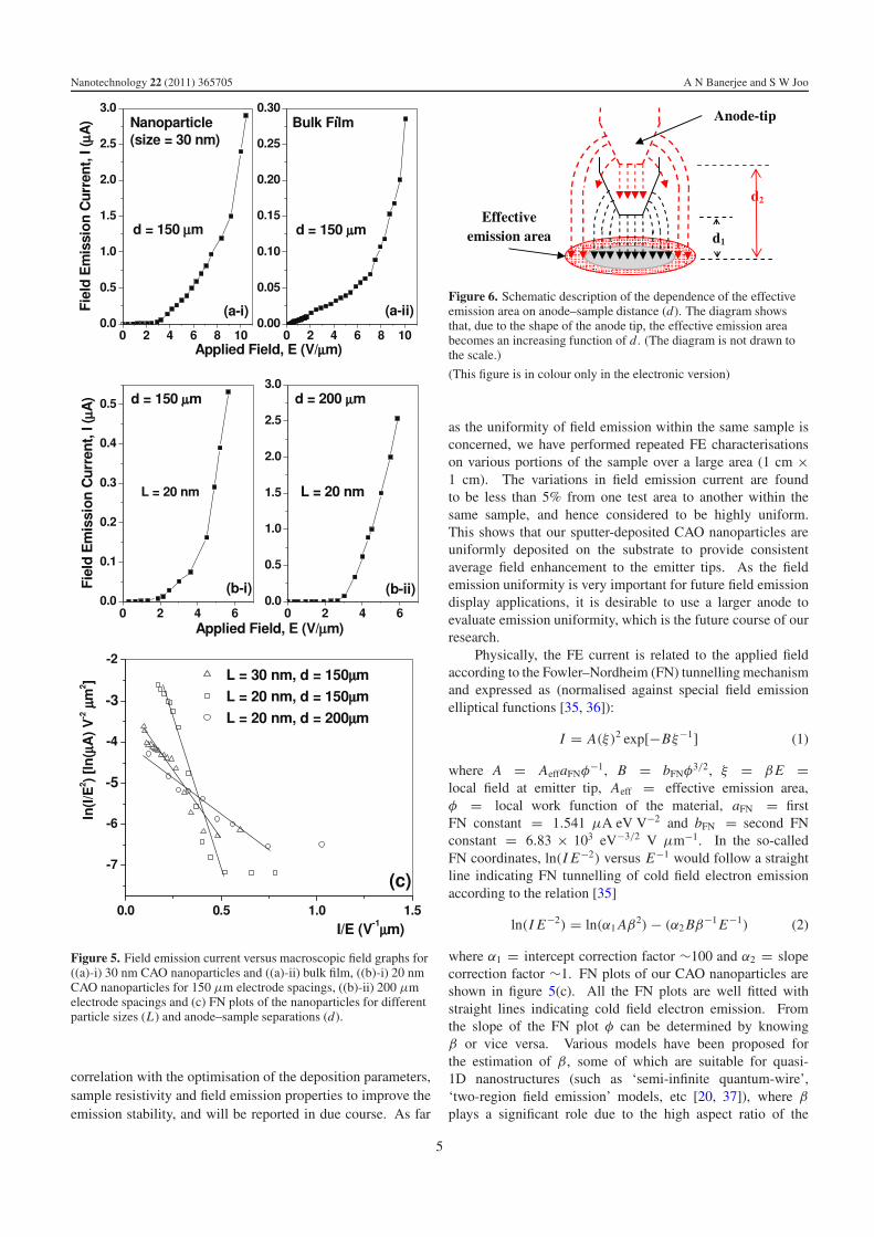
Figures 5((a)-i/ii) represent the FE current (I ) versusapplied field (E) of CAO nanoparticles and thin film depositedfor 20 and 60 min, respectively, with an anode–sample gap(d) of 150 μm. As-synthesised CAO thin film depositedfor 60 min is considered as bulk, since the film thicknessis much higher (∼250 nm) than the nanoparticle size (L ∼30 nm). Figures 5((b)-i/ii) show the same for (L =) 20 nm CAO nanoparticles for two different d values. TheFE characteristic of bulk film is presented here mainly tocompare with that of nanostructured CAO. Most of the FEproperties of the bulk film are similar to those reported byus previously [4, 5]. A comparison between the curves fornanoparticles and bulk film (cf table 1) depicts that the FEcurrents for nanoparticles are higher than those of the bulkfilm under identical applied field, although the turn-on field(defined as the applied field required to get an FE currentdensity of 1 μA cm−2) for bulk film (∼1.0 V μm−1) isslightly lower than that of nanoparticles (∼2.0–2.2 V μm−1).It is well known that the field enhancement factor β playsan important role for low-macroscopic field emission fromnanostructured materials. Sharp tips of the order of a fewnanometres provide the necessary enhancement of the appliedfield at the emitter tips for cold field electron emission.Although the field enhancement is higher in the nanoparticlefilms due to the low-dimensional structure of the sampleswith respect to the bulk film, but the packing density of thefield emission sites are higher in the bulk samples than thoseof nanoparticle films which are quasi-continuous, as shownfrom the TEM and AFM images. At lower fields, as onlya small fraction of the field emitters having high-β valuescontribute to the FE process, the bulk sample shows lowerturn-on field due to higher packing density. But at higherfields, proximity screening [32] becomes effective in the bulkfilm as more and more field emitters even with lower β
values tend to participate in the FE process, thus reducing theoverall current, as shown from the FE graphs. To confirmthat there are no morphological changes of the nanoparticlesamples during measurements, we have performed the I –Echaracterisations with increasing and decreasing E , andobserved no significant changes in the I –E curves within theexperimental limits. Hence proximity screening is consideredto be the probable reason for the large difference in theoverall FE currents between bulk and nanoparticle films. Itis noteworthy that the turn-on fields of our CAO nanoparticlesare comparable to the carbon and oxide-based nanomaterialslike CNTs, CNPs, ZnO nanorods, Si-C nanowires, etc(∼0.5–2.0 V μm−1) [22–25], but much lower than those ofconventional carbon-based thin film emitters like diamond,DLC, a:C, etc (∼5.0–20 V μm−1) [13–18] and hence canbecome potential alternative field-emitting materials for FEDs.
Also, in the I –E curves of the nanoparticle films depositedfor 10 min (figures 5(b)-i/ii), we have observed an increasein the emission current with an increase in the anode–sampleseparation (d) at a given applied field, although the nature ofthe curves remains identical. For example, at E = 5 V μm−1,I = 0.31 μA (for d = 150 μm) and 1.5 μA (for d =200 μm). The reason for this is probably due to the change inthe effective emission area of the sample for different anode–sample separation (d), which is related to the geometry ofthe anode tip as depicted in figure 6. As mentioned earlier,the anode in our experiment is conical in shape with a tipdiameter of 1.0 mm; therefore the lines of force emanatingfrom the edge of the anode tip and terminating at the samplesurface are diverging in nature, whereas the lines of forceemanating from the flat surface of the tip are parallel innature (neglecting the small surface roughness of the highlypolished stainless steel tip) [4, 5]. Therefore, the effectiveemission area of the sample becomes an increasing function ofthe anode–sample separation (d), as schematically describedin figure 6. Generally, most of the reported field emissionapparatus consists of a parallel plate arrangement of the anodeand the sample, separated by spacers [33]. So the electric linesof force between the anode and the sample are always moreor less parallel in nature (neglecting the fringing fields at theedges), hence the effective emission area remains independentof the anode–sample spacings. Therefore, unlike ours, in thesecases a decreasing trend of the emission current is observedwith the increase in the d value since the internal electric fielddecreases due to the large gap. Also, to verify that the currentincrement in our sample is whether, due to any morphologicalchanges in the sample or not, we have done the experimentin both ways: first, with increasing anode–sample spacingand, secondly, with decreasing anode–sample spacing. Butin both cases similar kinds of shifts in the I –E curves areobserved, indicating no (or almost negligible) morphologicalchanges within the sample during operation, thus supportingour arguments.
Also, the emission stability of CAO nanoparticle filmsis tested at a high vacuum of 10−7 mbar under a constantelectric field of 5.0 V μm−1 during 180 min while the currentdensity was kept at 0.31 μA (sample with L = 20 nm) and0.33 μA (for samples with L = 30 nm) at an electrodespacing (d) of 150 μm. The emission current fluctuation isfound to be less than 10%, which shows reasonable emissionstability compared to carbon-based field emitters [34]. Butbeyond 180 min, a 20% continuous degradation of the emissioncurrent is observed, which might be related to the highresistivity (∼50 � cm) of our quasi-continuous nanoparticlefilms. Hence, a detailed study of the sample propertiesbefore and after sustained field emission is underway in
4
Nanotechnology 22 (2011) 365705 A N Banerjee and S W Joo
Figure 5. Field emission current versus macroscopic field graphs for((a)-i) 30 nm CAO nanoparticles and ((a)-ii) bulk film, ((b)-i) 20 nmCAO nanoparticles for 150 μm electrode spacings, ((b)-ii) 200 μmelectrode spacings and (c) FN plots of the nanoparticles for differentparticle sizes (L) and anode–sample separations (d).
correlation with the optimisation of the deposition parameters,sample resistivity and field emission properties to improve theemission stability, and will be reported in due course. As far
Figure 6. Schematic description of the dependence of the effectiveemission area on anode–sample distance (d). The diagram showsthat, due to the shape of the anode tip, the effective emission areabecomes an increasing function of d . (The diagram is not drawn tothe scale.)
(This figure is in colour only in the electronic version)
as the uniformity of field emission within the same sample isconcerned, we have performed repeated FE characterisationson various portions of the sample over a large area (1 cm ×1 cm). The variations in field emission current are foundto be less than 5% from one test area to another within thesame sample, and hence considered to be highly uniform.This shows that our sputter-deposited CAO nanoparticles areuniformly deposited on the substrate to provide consistentaverage field enhancement to the emitter tips. As the fieldemission uniformity is very important for future field emissiondisplay applications, it is desirable to use a larger anode toevaluate emission uniformity, which is the future course of ourresearch.
Physically, the FE current is related to the applied fieldaccording to the Fowler–Nordheim (FN) tunnelling mechanismand expressed as (normalised against special field emissionelliptical functions [35, 36]):
I = A(ξ)2 exp[−Bξ−1] (1)
where A = AeffaFNφ−1, B = bFNφ3/2, ξ = β E =local field at emitter tip, Aeff = effective emission area,φ = local work function of the material, aFN = firstFN constant = 1.541 μA eV V−2 and bFN = second FNconstant = 6.83 × 10³ eV−3/2 V μm−1. In the so-calledFN coordinates, ln(I E−2) versus E−1 would follow a straightline indicating FN tunnelling of cold field electron emissionaccording to the relation [35]
ln(I E−2) = ln(α1 Aβ2) − (α2 Bβ−1 E−1) (2)
where α1 = intercept correction factor ∼100 and α2 = slopecorrection factor ∼1. FN plots of our CAO nanoparticles areshown in figure 5(c). All the FN plots are well fitted withstraight lines indicating cold field electron emission. Fromthe slope of the FN plot φ can be determined by knowingβ or vice versa. Various models have been proposed forthe estimation of β , some of which are suitable for quasi-1D nanostructures (such as ‘semi-infinite quantum-wire’,‘two-region field emission’ models, etc [20, 37]), where β
plays a significant role due to the high aspect ratio of the
5
Nanotechnology 22 (2011) 365705 A N Banerjee and S W Joo
nanowires/rods, whereas other models (like ‘hemisphere-on-a-post, hemiellipsoid-on-a-plane’, etc [19]) are suitable for thin-film-based emitters, where low (or negative) electron affinityand internal nanostructures play a more significant role thangeometrical field enhancement β [4, 16, 20–22]. As β ishighly dependent on the emitter-tip geometry, a suitable modelfor the calculation of β of sputter-deposited nanoparticles ischallenging because of the considerable statistical variationof the particle size (so also the tip geometry) of the as-synthesised CAO nanomaterials. Therefore, it is reasonable tofirst calculate the value of β from bulk film using the standardmodel to estimate the φ value from the corresponding FN plotand then using this φ value of the bulk film one can estimatethe β value for nanoparticles. Previously, we have shown that,for CAO bulk film, the field emission mechanism is dominatedby the low electron affinity and internal nanostructure of widebandgap CAO [4, 5]. Calculation of β using the hemisphere-on-a-post model [19] gives a value around 180–200 and thecorresponding φ value (calculated from FN plots) obtained as0.2 eV. This low value of φ is assumed to be some barrierpotential, equivalent to a barrier height H before Schottkylowering and, depending on the mode of emission, gives anestimation of electron affinity χ [15], which is considerablylower due to the wide bandgap of CAO (∼3.70 eV, discussedlater), as explained for p-type semiconducting diamond filmshaving a large bandgap (∼5.6 eV) [17, 38, 39]. Usingthis value of φ in the FN plots of CAO nanoparticles (cffigure 5(c)), the value of β is obtained as around 200–230 which is higher than that of bulk film and is expectedbecause, in CAO nanoparticles, due to the low-dimensionalstructure of the nanomaterial, the FE mechanism is consideredto be a combination of internal nanostructure (electricallynanostructured heterogeneous {ENH} material, discussedbelow), band structure (low electron affinity) and high-β(greater field enhancement) effects. The low-dimensionalstructure tends to increase the β value, which in turn increasesthe overall FE current considerably, whereas the low valueof electron affinity manifests a dominant non-degenerateconduction band emission for low-threshold field electronemission. And last but not least, the internal ENH structureof the material with quasi-filamentary conducting channelsinside a less-conducting matrix manifests considerable fieldenhancement within the nanoparticles for the sustained fieldelectron emission due to the continuous injection of electronsinto the conduction band inside the material [15]. It is wellknown that the work function is highly dependent on thesurface structure of the emitting materials. The conventionaldefinition of work function relates to a large, clean, flat surfaceof uniform crystallographic structure. Therefore for thin filmand nanocrystalline materials with high surface roughness likeours, φ will be much different from that of a flat band surface.Hence, we have defined φ as the ‘local work function’ todistinguish it from the flat band work function (φFB). Also,due to the large geometrical field enhancement at the low-dimensional emitter tips in our nanocrystalline samples, thelocal field will be strong enough (∼ V nm−1) to create bandbending to modify the value of φ [15]. Therefore, consideringthe image type forces, the barrier height H seen by an electron
at the Fermi level will be much less than φFB, due to theSchottky lowering effect. Therefore it is reasonable to assumethis low value of φ as equivalent to some barrier potentialbefore Schottky lowering, as stated above. Also it is reasonableto assume dominant non-degenerate conduction band (CB)emission in our samples, rather than degenerate CB emission,because of the high resistivity of our samples which hindersthe bulk carrier transport under the operative field domain [15].But, it is pertinent to state in this connection that the presenceof some surface states in this type of nanocrystalline samplescannot be ruled out, which may contribute to the fieldenhancement as a secondary effect. Therefore a detailed studyis necessary to understand the actual emission mechanism inthis kind of material, which is the future course of our research.
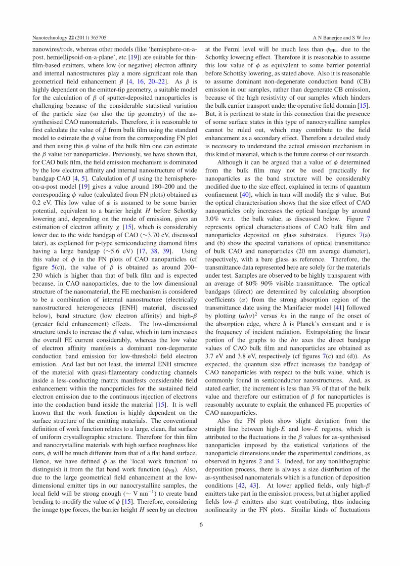
Although it can be argued that a value of φ determinedfrom the bulk film may not be used practically fornanoparticles as the band structure will be considerablymodified due to the size effect, explained in terms of quantumconfinement [40], which in turn will modify the φ value. Butthe optical characterisation shows that the size effect of CAOnanoparticles only increases the optical bandgap by around3.0% w.r.t. the bulk value, as discussed below. Figure 7represents optical characterisations of CAO bulk film andnanoparticles deposited on glass substrates. Figures 7(a)and (b) show the spectral variations of optical transmittanceof bulk CAO and nanoparticles (20 nm average diameter),respectively, with a bare glass as reference. Therefore, thetransmittance data represented here are solely for the materialsunder test. Samples are observed to be highly transparent withan average of 80%–90% visible transmittance. The opticalbandgaps (direct) are determined by calculating absorptioncoefficients (α) from the strong absorption region of thetransmittance date using the Manifacier model [41] followedby plotting (αhν)2 versus hν in the range of the onset ofthe absorption edge, where h is Planck’s constant and ν isthe frequency of incident radiation. Extrapolating the linearportion of the graphs to the hν axes the direct bandgapvalues of CAO bulk film and nanoparticles are obtained as3.7 eV and 3.8 eV, respectively (cf figures 7(c) and (d)). Asexpected, the quantum size effect increases the bandgap ofCAO nanoparticles with respect to the bulk value, which iscommonly found in semiconductor nanostructures. And, asstated earlier, the increment is less than 3% of that of the bulkvalue and therefore our estimation of β for nanoparticles isreasonably accurate to explain the enhanced FE properties ofCAO nanoparticles.
Also the FN plots show slight deviation from thestraight line between high-E and low-E regions, which isattributed to the fluctuations in the β values for as-synthesisednanoparticles imposed by the statistical variations of thenanoparticle dimensions under the experimental conditions, asobserved in figures 2 and 3. Indeed, for any nonlithographicdeposition process, there is always a size distribution of theas-synthesised nanomaterials which is a function of depositionconditions [42, 43]. At lower applied fields, only high-βemitters take part in the emission process, but at higher appliedfields low-β emitters also start contributing, thus inducingnonlinearity in the FN plots. Similar kinds of fluctuations
6

Nanotechnology 22 (2011) 365705 A N Banerjee and S W Joo
Figure 7. Optical transmittance spectra of (a) CAO bulk film, (b) nanoparticle of average diameter of 20 nm, (c) bandgap calculation for bulkCAO film and (d) for CAO nanoparticles of average diameter of 20 nm.
in the FN plots are also observed by other groups andexplained similarly in terms of variations in β values [44, 45].Also the experimental FN plot, shown in equation (2), isactually modelled at the mid-range of the experimental data,as explained by Forbes [35]. Therefore, we have also fitted thestraight line at the mid-range of the experimental FN data toget the estimation of FE properties of our samples, which arereasonably accurate.
4. Conclusions
FE properties of CAO nanoparticles have been investigatedfor the first time. Nanoparticles are deposited via the dcsputtering technique on glass and silicon substrates. Thesize of the nanoparticles is varied by changing the depositiontime. TEM micrographs confirm the average particle diametersaround 20–30 nm. XRD measurements confirm the properphase formation of the nanomaterials. FE studies of CAOnanoparticles show that the FE mechanism is according tothe standard Fowler–Nordheim tunnelling of cold electronemission. FE properties of the nanoparticles are found tobe better than that of bulk CAO film due to the combinedeffects of low electron affinity, internal nanostructure and largefield enhancement at the low-dimensional emitter tips of theCAO nanoparticles. The field enhancement factor is foundto be around 230 with a turn-on field around 2 V μm−1,which is considerably lower and comparable to conventionalcarbon-based field emitters, and therefore can become potentialalternative materials for field emission displays.
Acknowledgments
Financial support of the WCU grant no. R32-2008-000-20082-0 of the Ministry of Education, Sci. & Technol. of Korea is
acknowledged. Also we are grateful to Dr K K Chattopadhyay,Jadavpur University, India and Dr R G Forbes, University ofSurrey, UK for useful technical support/discussions.
References
[1] Banerjee A N and Chattopadhyay K K 2005 Prog. Cryst.Growth Charact. Mater. 50 52
[2] Kawazoe H, Yasukawa M, Yanagai H and Hosono H 1997Nature 389 939
[3] Thomas G 1997 Nature 389 907[4] Banerjee A N, Ghosh C K, Das S and Chattopadhyay K K 2005
Physica B 370 264[5] Banerjee A N and Chattopadhyay K K 2004 Appl. Surf. Sci.
225 243[6] Banerjee A N, Maity R, Ghosh P K and Chattopadhyay K K
2005 Thin Solid Films 474 261[7] Kunihito K, Hisashi K and Seon S W 2001 J. Mater. Chem.
11 251[8] Park K, Ko K Y, Kwon H C and Nahm S 2007 J. Alloys
Compounds 437 1[9] Zheng X G, Taniguchi K, Takahashi A, Liu Y and Xu C N 2004
Appl. Phys. Lett. 85 1728[10] Smith J R, Van Steenkiste T H and Wang X G 2009 Phys. Rev.
B 79 041403[11] Kizaki H, Sato K, Yanase A and Yoshida H K 2006 Physica B
376/377 812[12] Fink R L, Tolt Z L and Yaniv Z 1998 Surf. Coat. Technol.
108/109 570[13] May P W, Hohn S, Wang W N and Fox N A 1998 Appl. Phys.
Lett. 72 2182[14] Baek Y G, Ikuno T, Ryu J T, Honda S I, Katayama M,
Oura K and Hirao T 2002 Appl. Surf. Sci. 185 243[15] Forbes R G 2001 Solid State Electron. 45 779[16] Groing O, Kuttel O M, Groing P and Schlapbach L 1997 Appl.
Phys. Lett. 71 2253[17] Robertson J 1996 Diamond Relat. Mater. 5 797[18] Robertson J 1997 Thin Solid Films 296 61
7

Nanotechnology 22 (2011) 365705 A N Banerjee and S W Joo
[19] Forbes R G, Edgcombe C J and Valdre U 2003Ultramicroscopy 95 57
[20] Banerjee A N, Qian S and Joo S W 2011 Nanotechnology22 035702
[21] Joo S W and Banerjee A N 2010 J. Appl. Phys. 107 114317[22] Chen C, Lin C and Wang C 2003 Appl. Phys. Lett. 82 2515[23] Maity R, Banerjee A N and Chattopadhyay K K 2004 Appl.
Surf. Sci. 236 231[24] Zhou X T, Lai H L, Peng H Y, Au F C K, Liao L S, Wang N,
Bello I, Lee C S and Lee S T 2000 Chem. Phys. Lett. 318 58[25] Yu J, Wang E G and Bai X D 2001 Appl. Phys. Lett. 78 2226[26] Ahmed A, Jagdale T, Dhas V, Khan S, Patil S, Pasricha R,
Ravi V and Ogale S 2007 Adv. Mater. 19 3295[27] Gao S, Zhao Y, Guo P, Chen N and Xie Y 2003
Nanotechnology 14 538[28] Banerjee A N and Chattopadhyay K K 2005 J. Appl. Phys.
97 084302[29] Banerjee A and Das B 2008 Rev. Sci. Instrum. 79 033910[30] Park Y R, Jung D, Kim K-C, Suh S J, Park T S and
Kim Y S 2009 J. Eletroceram. 23 536[31] Chan T-C, Chen K-C and Liao C-N 2011 Appl. Phys. Lett.
98 181902
[32] Nilsson L, Groening O, Emmenegger C, Kuttel O, Schaller E,Schlapbach L, Kind H, Bonard J M and Kern K 2000 Appl.Phys. Lett. 76 2071
[33] Okano K, Koizumi S, Silva S R P and Amartunga G A J 1996Nature 381 140
[34] Uppireddy K, Rao C V, Ishikawa Y, Weiner B R andMorell G 2010 Appl. Phys. Lett. 97 062106
[35] Forbes R G 1999 Ultramicroscopy 79 11[36] Murphy E L and Good R H 1956 Phys. Rev. 102 1464[37] Zhong D Y, Zhang G Y, Liu S, Sakurai T and Wang E G 2002
Appl. Phys. Lett. 80 506[38] Latham R V 1983 IEEE Trans. Electr. Insul. 18 194[39] Hirakuri K K, Ohyama M, Komura N, Sudo K and Sato K 2005
J. Appl. Phys. 97 023516[40] Brus L E 1984 J. Chem. Phys. 80 4403[41] Manifacier J C, Gasiot J and Fillard J P 1976 J. Phys. E: Sci.
Instrum. 9 1002[42] Banerjee A N, Krisna R and Das B 2008 Appl. Phys. A 90 299[43] Das B and Banerjee A 2007 Nanotechnology 18 445202[44] Chen J, Deng S Z, Wen X and Yang S 2003 J. Appl. Phys.
93 1774[45] Kumar A, Avasthi D K, Tripathi A, Filip L D, Carey J D and
Pivin J C 2007 J. Appl. Phys. 102 044305
8
Copyright © 2022 FDOKUMEN