Low Bit Rate Design and Implementation of BPSK Demodulation on FPGA
10
International Journal of Modern Engineering Research (IJMER) www.ijmer.com Vol. 3, Issue. 3, May.-June. 2013 pp- 1748-1755 ISSN: 2249-6645 Low Bit Rate Design and Implementation of BPSK Demodulation on FPGA Nehal.A.Ranabhatt 1 , Sudhir Agarwal 2 *(EC Department, L.C.Institute of Technology,Bhandu, India) ** (DCTD Department, Space Application center ,ISRO,Ahmedabad, India ABSTRACT: This paper présents extended Works on BPSK Modulation at Low Bit Rate and also presents Simulation results and FPGA implementation of BPSK demodulation at Low Bit Rate 1200 bits/second on Altera Stratix III Development Board. Here Binary Sequence ,Carrier Frequency and sampling frequency are user controllable in BPSK modulation that was designed already. So this paper present Design of BPSK Demodulation which demodulate pattern comes at output of BPSK modulation at 1200 bits/second. BPSK demodulation technique was analyzed using QuartusII 9.1 Complier. Design of BPSK Demodulation is completed using VHSIC (Very High Speed Integrated Circuit) Hardware Description Language (VHDL). In BPSK Design one Mega Function ROM is used .BPSK Demodulation was done in Continuous mode. Here system Performance is measured in Noise by measuring BER of system and comparing BER performance to Ideal Theoretical performance. Keywords: BPSK Demodulation, BPSK Modulation, Bits Per Second, Low Bit rate, FPGA, Bit Error Rate I. INTRODUCTION The aim of the paper is to create a BPSK (Binary Phase Shift Keying) Demodulator which demodulates the Modulated signal comes from Modulator which has Bit rate 1200 bps. First we give Introduction about coherent BPSK Demodulation and then BPSK Demodulation is designed and Implemented on StratixIII FPGA. This paper presents extended work of RTL Design and Implementation of BPSK Modulation at Low Bit Rate .In this BPSK Modulation is Design and Implement at low Bit Rate 1200 bps[1]. Fig.1 Coherent BPSK Demodulation[2] In coherent detection technique the knowledge of the carrier frequency and phase must be known to the receiver. This can be achieved by using a PLL (phase lock loop) at the receiver. A PLL essentially locks to the incoming carrier frequency and tracks the variations in frequency and phase. For demonstration purposes we simply assume that the carrier phase recovery is done and simply use the generated reference frequency at the receiver (sin(ωt)).In the demodulator the received signal is multiplied by a reference frequency generator. The multiplied output is integrated over one bit period using an integrator. A threshold detector makes a decision on each integrated bit based on a threshold. Since an NRZ signaling format is used with equal amplitudes in positive and negative direction, the threshold for this case would be “0”.[2] Simulation Results for BPSK Demodulation are carried out using ModelSim-Altera 6.5b (Quartus II 9.1).BPSK demodulation is designed for
-
Upload
independent -
Category
Documents
-
view
0 -
download
0
Transcript of Low Bit Rate Design and Implementation of BPSK Demodulation on FPGA

International Journal of Modern Engineering Research (IJMER) www.ijmer.com Vol. 3, Issue. 3, May.-June. 2013 pp-
1748-1755 ISSN: 2249-6645
Low Bit Rate Design and Implementation of BPSK Demodulation on FPGA
Nehal.A.Ranabhatt1, Sudhir Agarwal2
*(EC Department, L.C.Institute of Technology,Bhandu, India) ** (DCTD Department, Space Application center ,ISRO,Ahmedabad, India
ABSTRACT: This paper présents extended Works on BPSK Modulation at Low Bit Rate and also presents Simulation results and FPGA implementation of BPSK demodulation at Low Bit Rate 1200 bits/second on Altera Stratix III Development Board. Here Binary Sequence ,Carrier Frequency and sampling frequency areuser controllable in BPSK modulation that was designed already. So this paper present Design of BPSK Demodulation which demodulate pattern comes at output of BPSK modulation at 1200 bits/second. BPSK demodulation technique was analyzed using QuartusII 9.1 Complier. Design of BPSK Demodulation is completed using VHSIC (Very High Speed Integrated Circuit) Hardware Description Language (VHDL). In BPSK Design one Mega Function ROM is used .BPSK Demodulation was done in Continuous mode. Heresystem Performance is measured in Noise by measuring BER of system and comparing BER performance to Ideal Theoretical performance. Keywords: BPSK Demodulation, BPSK Modulation, Bits Per Second, Low Bit rate, FPGA, Bit Error Rate
I. INTRODUCTIONThe aim of the paper is to create a BPSK (Binary Phase Shift Keying) Demodulatorwhich demodulates
the Modulated signal comes from Modulator which has Bit rate 1200 bps. First we give Introduction aboutcoherent BPSK Demodulation and then BPSK Demodulation is designed and Implemented on StratixIII FPGA.This paper presents extended work of RTL Design and Implementation of BPSK Modulation at Low Bit Rate.In this BPSK Modulation is Design and Implement at low Bit Rate 1200 bps[1].
Fig.1 Coherent BPSK Demodulation[2]
In coherent detection technique the knowledge of the carrier frequency and phase
must be known to the receiver. This can be achieved by using a PLL (phase lock loop) at the receiver. A PLLessentially locks to the incoming carrier frequency and tracks the variations in frequency and phase. For demonstration purposes we simply assume that the carrier phase recovery is done and simply use the generated reference frequency at the receiver (sin(ωt)).In the demodulator the received signal is multiplied by a referencefrequency generator. The multiplied output is integrated over one bit period using an integrator. A threshold detector makes a decision on each integrated bit based on a threshold. Since an NRZ signaling format is used with equal amplitudes in positive and negative direction, the threshold for this case would be “0”.[2]Simulation Results for BPSK Demodulation are carried out using ModelSim-Altera 6.5b (Quartus II 9.1).BPSK demodulation is designed for

Altera Stratix III FPGA development Board and the device used is EP3SL150F1152c2.
II. CONCEPT OF BPSK DEMODULATIONIn BPSK demodulator design modulated bit pattern is given as Input. Samples per bits are fetched in
sequence. Then samples of one bit is fetched from Modulated Pattern, are multiplied with Positive and Negative carrier samples. Sum of multiplication output will store in two different arrays. Subtraction block will perform subtraction of two different array in which sum of multiplication output is stored. Comparison block do thecomparison based on output of subtraction block.
www.ijmer.com 1748 | Page

International Journal of Modern Engineering Research (IJMER) www.ijmer.com Vol. 3, Issue. 3, May.-June. 2013 pp-
1748-1755 ISSN: 2249-6645
Fig.2. Principal of BPSK Demodulation[2]If subtraction of samples is grater then zero then bit“1” is detected and if subtraction of samples is less
then zero then bit “0” is detected at output of demodulator.[2]
III. BPSK DEMODULATION DESIGN ON FPGA
Fig.3.Principal of BPSK Demodulation FPGA Fig.2 shows basic concept of BPSK demodulation on FPGA. First BPSK modulated output works as
input of BPSK demodulation. Then Modulated output passed through analog to digital converter. Then samples per bit and samples of ROM are converted in Positive to Negative range. After this ADCsamples are multiply with Positive and Negative samples of sine wave and Added in two different accumulator. Output of accumulators are compared with each other means if value of accumulator1 is grater then accumulator 2 then output is 1 else output is 0.
In this design we have used one Altera MegaFuctions of single port ROM used to store the 10,000 sine
wave samples. Incoming clock from ADC is of 120 MHz and entire demodulation design operates on it.1 bitprevails for 1 lakh counter at 120 MHz so we have a counter that counts up to 1 lakh and rollovers. This counter used for generating the demod bit every 1 lakh count. Sine wave address generation logic generates the address for the sine wave samples ROM depending on the carrier frequency constant and samplingfrequency constant and counter_10.

Fig.4.Design of BPSK Demodulation on FPGA ADC samples are latched and sine wave sample fetched from ROM are latched. Also 180 degree phase
shifted sample value is found by subtracting the sample from 3ffe and it is also latched. All the above 3 samples are in range 0 to x”3fffe” and binary offset format, where 0 is equal to x”1fff”, positive numbers are in between x”2000 “ to x”3ffe” and negative numbers are in between 0 to x”1fffe”. For demodulation we bring them in range – x”1fff” to + x”1fff”. This we do by converting the numbers in range 0 to x”1fff” and generating the sign bit equal to 1 if negative. Thus for numbers x”1fff” to x”3fffe” we subtract x”1fff” and generate sign bit 0 whilefor nos 0 to x”1ffe” we subtract them from x”1fff” and generate sign bit 1, indicatingnegative.Positive value
www.ijmer.com 1749 | Page

International Journal of Modern Engineering Research (IJMER) www.ijmer.com Vol. 3, Issue. 3, May.-June. 2013 pp-
1748-1755 ISSN: 2249-6645conversion and sign bit generation does the above process for all the 3 values.Multiplication and sign generation logic multiplies the positive ADC sample with positive sample and positive sample 180 degree shifted of the ROM. Sign of the two multiplication operations is generated depending on the sign of the samples determined in the previous process.For accumulation purpose we convert the two multiplied values in 2’s complement form using the sign bit of each values.Then both the values are added to their respective accumulators. On every 1 lakh count the two accumulator values are compared, if accumulator 1 is greater than accumulator 2 then the bitis decoded as 1 else 0.
IV.SIMULATION RESULTS FOR BPSK DEMODULATION
Fig. 5. Reason for getting 1 Bit Delay in Demodulation Output Fig .5 shows that when Demodulation will start up to one bit ADC data will remain undefined so up 1
bit Demodulation operation can not be started.so we get 1 Bit Delay at output of BPSK Demodulation.
Fig 6. BPSK Demodulation output when fs=12MHz,
fc=18K,br=1200 Fig .6 shows BPSK demodulation when fs=12MHz,fc=18KHz and Br=1200 bps.

Fig 7. BPSK Demodulation output when fs=12MHz, fc=18K,br=1200
Fig .7 shows remaining signal at output of BPSK Demodulation as shown in Fig.6.
www.ijmer.com 1750 | Page
International Journal of Modern Engineering Research (IJMER) www.ijmer.com Vol. 3, Issue. 3, May.-June. 2013 pp-
1748-1755 ISSN: 2249-6645
Fig 8. BPSK Demodulation output when fs=12MHz, fc=18K,br=1200 Fig .8 shows Debugging at one sample. Here after all calculation according to program acc1>acc2 so demod_bit will 0 that can be proved from simulation results.
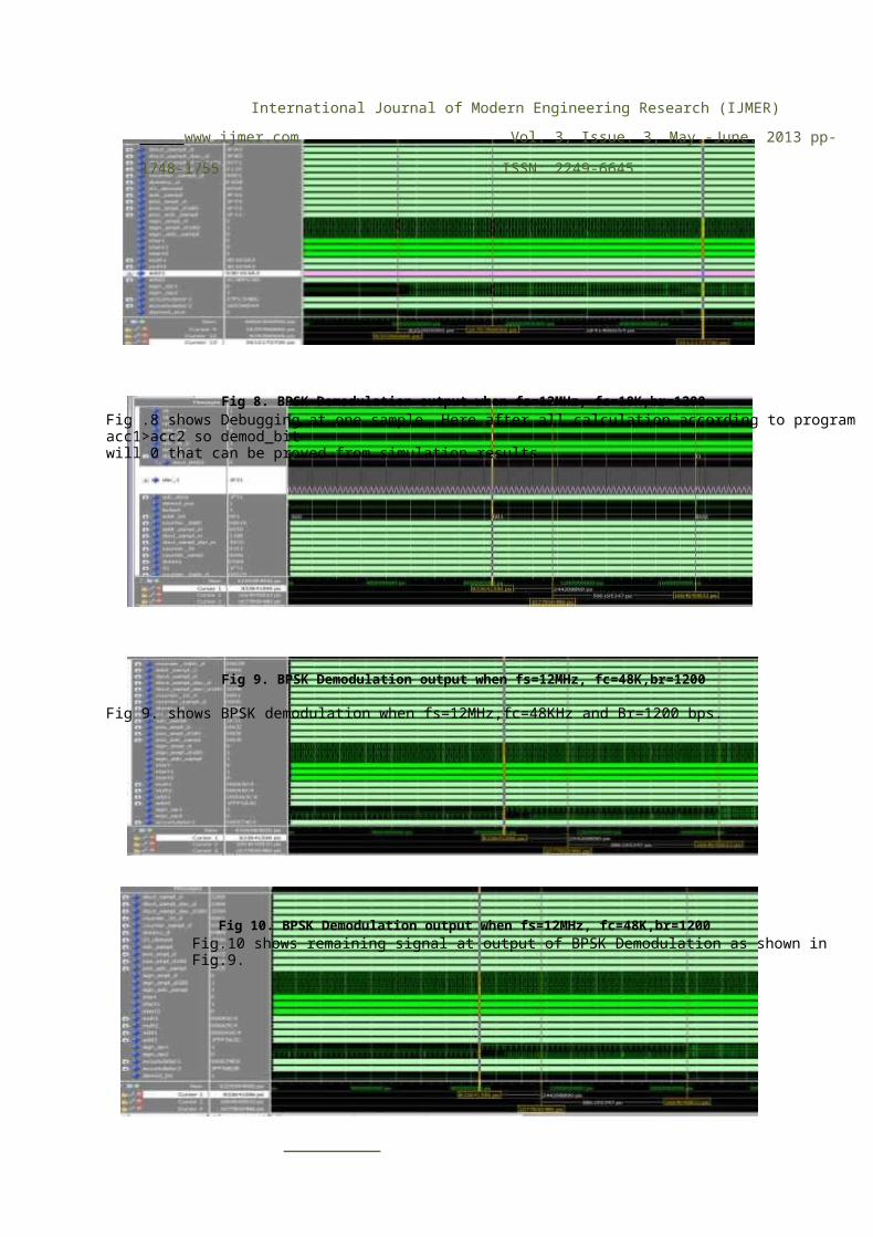
Fig 9. BPSK Demodulation output when fs=12MHz, fc=48K,br=1200
Fig 9. shows BPSK demodulation when fs=12MHz,fc=48KHz and Br=1200 bps.
Fig 10. BPSK Demodulation output when fs=12MHz, fc=48K,br=1200 Fig.10 shows remaining signal at output of BPSK Demodulation as shown in Fig.9.

www.ijmer.com
1751 | Page

International Journal of Modern Engineering Research (IJMER) www.ijmer.com Vol. 3, Issue. 3, May.-June. 2013 pp-
1748-1755 ISSN: 2249-6645Fig 11. BPSK Demodulation output when fs=12MHz, fc=18K,br=1200
Fig .11 shows Debugging at one sample. Here after all calculation according to program acc1<acc2 so demod_bit will 0 that can be proved from simulation results.
V. REAL TIME RESULTS FOR BPSK DEMODULATION
Fig.12 BPSK Demodulation Output On Oscilloscope When fs=12MHz fc=18KHz
Fig13 Experimental set up for BPSK Demodulation When fs=12MHz fc=18KHz
Fig.14 BPSK Demodulation oscilloscope When fs=12MHz fc=18KHz
Fig.15 Experimental set up for BPSK Demodulation When fs=12MHz fc=48KHz Fig 12,14, shows real time results on Oscilloscope for different carrier frequency 18k,48k respectively.Fig13,15 shows experimental set uo for BPSK Demodulation at low Bit Rate 1200bps with carrier frequency 18k,48k respectively.
VI.CALCULATION OF BIT ERROR RATETo calculate Bit error rate of BPSK system first we add 20MHZ noise in BPSK Modulation spectrum.
Then take fc+fm component that is 20.048MHz as center frequency. After that we take plain carrier and measure C/N0 for diffent level. After getting different C/N0 fom this value we can obtain value of Eb/N0 and then we can plot BER versus Eb/No curve which will show the performance of system. Here we compare system performance with standard theoretical value BER curve. C/N0 can be measured in dbc/Hz means it will

measure carrier power in 1Hz noise bandwidth and here we take -20dbm reference level for C/N0 calculation. Resolution bandwidth is 500Hz.Eb/N0 can obtain from following formula. Eb/N0(db)=10 log(C/N0)-10 log(1200)
Spectrum Results for Calculation of Different C/N0
www.ijmer.com 1752 | Page