LM5067 Negative Hot Swap / Inrush Current Controller with ...
50
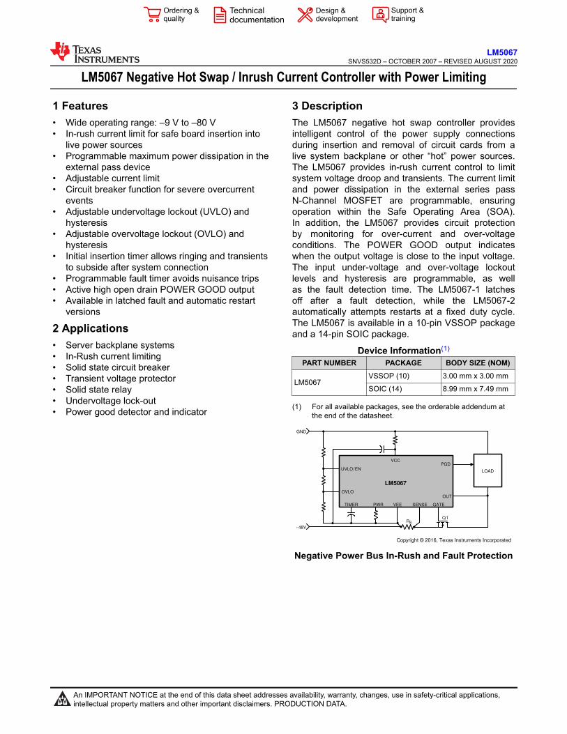
LM5067 Negative Hot Swap / Inrush Current Controller with Power Limiting 1 Features • Wide operating range: –9 V to –80 V • In-rush current limit for safe board insertion into live power sources • Programmable maximum power dissipation in the external pass device • Adjustable current limit • Circuit breaker function for severe overcurrent events • Adjustable undervoltage lockout (UVLO) and hysteresis • Adjustable overvoltage lockout (OVLO) and hysteresis • Initial insertion timer allows ringing and transients to subside after system connection • Programmable fault timer avoids nuisance trips • Active high open drain POWER GOOD output • Available in latched fault and automatic restart versions 2 Applications • Server backplane systems • In-Rush current limiting • Solid state circuit breaker • Transient voltage protector • Solid state relay • Undervoltage lock-out • Power good detector and indicator 3 Description The LM5067 negative hot swap controller provides intelligent control of the power supply connections during insertion and removal of circuit cards from a live system backplane or other “hot” power sources. The LM5067 provides in-rush current control to limit system voltage droop and transients. The current limit and power dissipation in the external series pass N-Channel MOSFET are programmable, ensuring operation within the Safe Operating Area (SOA). In addition, the LM5067 provides circuit protection by monitoring for over-current and over-voltage conditions. The POWER GOOD output indicates when the output voltage is close to the input voltage. The input under-voltage and over-voltage lockout levels and hysteresis are programmable, as well as the fault detection time. The LM5067-1 latches off after a fault detection, while the LM5067-2 automatically attempts restarts at a fixed duty cycle. The LM5067 is available in a 10-pin VSSOP package and a 14-pin SOIC package. Device Information (1) PART NUMBER PACKAGE BODY SIZE (NOM) LM5067 VSSOP (10) 3.00 mm x 3.00 mm SOIC (14) 8.99 mm x 7.49 mm (1) For all available packages, see the orderable addendum at the end of the datasheet. GND VCC VEE SENSE TIMER UVLO/EN GATE OVLO PGD LM5067 PWR OUT LOAD R S Q1 - 48V Copyright © 2016, Texas Instruments Incorporated Negative Power Bus In-Rush and Fault Protection LM5067 SNVS532D – OCTOBER 2007 – REVISED AUGUST 2020 An IMPORTANT NOTICE at the end of this data sheet addresses availability, warranty, changes, use in safety-critical applications, intellectual property matters and other important disclaimers. PRODUCTION DATA.
-
Upload
khangminh22 -
Category
Documents
-
view
1 -
download
0
Transcript of LM5067 Negative Hot Swap / Inrush Current Controller with ...
LM5067 Negative Hot Swap / Inrush Current Controller with Power Limiting
1 Features• Wide operating range: –9 V to –80 V• In-rush current limit for safe board insertion into
live power sources• Programmable maximum power dissipation in the
external pass device• Adjustable current limit• Circuit breaker function for severe overcurrent
events• Adjustable undervoltage lockout (UVLO) and
hysteresis• Adjustable overvoltage lockout (OVLO) and
hysteresis• Initial insertion timer allows ringing and transients
to subside after system connection• Programmable fault timer avoids nuisance trips• Active high open drain POWER GOOD output• Available in latched fault and automatic restart
versions
2 Applications• Server backplane systems• In-Rush current limiting• Solid state circuit breaker• Transient voltage protector• Solid state relay• Undervoltage lock-out• Power good detector and indicator
3 DescriptionThe LM5067 negative hot swap controller provides intelligent control of the power supply connections during insertion and removal of circuit cards from a live system backplane or other “hot” power sources. The LM5067 provides in-rush current control to limit system voltage droop and transients. The current limit and power dissipation in the external series pass N-Channel MOSFET are programmable, ensuring operation within the Safe Operating Area (SOA). In addition, the LM5067 provides circuit protection by monitoring for over-current and over-voltage conditions. The POWER GOOD output indicates when the output voltage is close to the input voltage. The input under-voltage and over-voltage lockout levels and hysteresis are programmable, as well as the fault detection time. The LM5067-1 latches off after a fault detection, while the LM5067-2 automatically attempts restarts at a fixed duty cycle. The LM5067 is available in a 10-pin VSSOP package and a 14-pin SOIC package.
Device Information(1)
PART NUMBER PACKAGE BODY SIZE (NOM)
LM5067VSSOP (10) 3.00 mm x 3.00 mm
SOIC (14) 8.99 mm x 7.49 mm
(1) For all available packages, see the orderable addendum at the end of the datasheet.
GND
VCC
VEE SENSETIMER
UVLO/EN
GATE
OVLO
PGD
LM5067
PWR
OUT
LOAD
RSQ1
- 48V
Copyright © 2016, Texas Instruments Incorporated
Negative Power Bus In-Rush and Fault Protection
LM5067SNVS532D – OCTOBER 2007 – REVISED AUGUST 2020
An IMPORTANT NOTICE at the end of this data sheet addresses availability, warranty, changes, use in safety-critical applications, intellectual property matters and other important disclaimers. PRODUCTION DATA.
Table of Contents1 Features............................................................................12 Applications..................................................................... 13 Description.......................................................................14 Revision History.............................................................. 25 Device Comparison......................................................... 36 Pin Configuration and Functions...................................4
Pin Functions.................................................................... 47 Specifications.................................................................. 5
7.1 Absolute Maximum Ratings........................................ 57.2 ESD Ratings............................................................... 57.3 Recommended Operating Conditions.........................57.4 Thermal Information....................................................57.5 Electrical Characteristics.............................................67.6 Switching Characteristics............................................77.7 Typical Characteristics................................................ 8
8 Detailed Description......................................................128.1 Overview................................................................... 12
8.2 Functional Block Diagram......................................... 138.3 Feature Description...................................................138.4 Device Functional Modes..........................................18
9 Application and Implementation.................................. 199.1 Application Information............................................. 199.2 Typical Application.................................................... 19
10 Power Supply Recommendations..............................3710.1 Operating Voltage................................................... 37
11 Layout...........................................................................3711.1 Layout Guidelines................................................... 3711.2 Layout Example...................................................... 38
12 Device and Documentation Support..........................3912.1 Trademarks.............................................................3912.2 Electrostatic Discharge Caution..............................3912.3 Glossary..................................................................39
13 Mechanical, Packaging, and Orderable Information.................................................................... 40
4 Revision HistoryChanges from Revision C (March 2013) to Revision D (August 2020) Page• Added ESD Rating table, Feature Description section, Device Functional Modes, Application and
Implementation section, Power Supply Recommendations section, Layout section, Device and Documentation Support section, and Mechanical, Packaging, and Orderable Information section .................. 1
• Updated the numbering format for tables, figures and cross-references throughout the document...................1• Updated Applications section............................................................................................................................. 1• Deleted text : "LM5067A is available..." .............................................................................................................1
Changes from Revision B (September 2009) to Revision C (March 2013) Page• Changed layout of National Data Sheet to TI format........................................................................................ 30
LM5067SNVS532D – OCTOBER 2007 – REVISED AUGUST 2020 www.ti.com
2 Submit Document Feedback Copyright © 2022 Texas Instruments Incorporated
Product Folder Links: LM5067
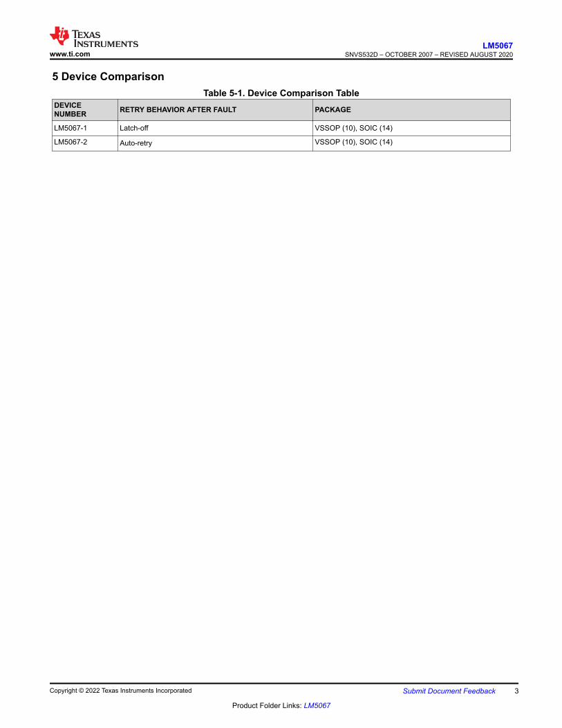
5 Device ComparisonTable 5-1. Device Comparison Table
DEVICE NUMBER RETRY BEHAVIOR AFTER FAULT PACKAGE
LM5067-1 Latch-off VSSOP (10), SOIC (14)
LM5067-2 Auto-retry VSSOP (10), SOIC (14)
www.ti.comLM5067
SNVS532D – OCTOBER 2007 – REVISED AUGUST 2020
Copyright © 2022 Texas Instruments Incorporated Submit Document Feedback 3
Product Folder Links: LM5067
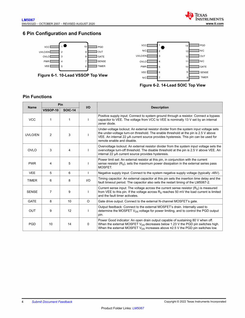
6 Pin Configuration and Functions
1
2
3
4
5
10
9
8
7
6
UVLO/EN
OVLO
PWR
VEE TIMER
PGD
OUT
VCC
GATE
SENSE
Figure 6-1. 10-Lead VSSOP Top View
1
2
3
4
5
11
10
9
87
6
UVLO/EN
OVLO
PWR
VEE
VCC
12
13
14
N/C
N/C
OUT
N/C
GATE
SENSE
PGD
TIMER
N/C
Figure 6-2. 14-Lead SOIC Top View
Pin Functions
NamePin
I/O DescriptionVSSOP-10 SOIC-14
VCC 1 1 IPositive supply input: Connect to system ground through a resistor. Connect a bypass capacitor to VEE. The voltage from VCC to VEE is nominally 13 V set by an internal zener diode.
UVLO/EN 2 3 I
Under-voltage lockout: An external resistor divider from the system input voltage sets the under-voltage turn-on threshold. The enable threshold at the pin is 2.5 V above VEE. An internal 22 µA current source provides hysteresis. This pin can be used for remote enable and disable.
OVLO 3 4 IOvervoltage lockout: An external resistor divider from the system input voltage sets the overvoltage turn-off threshold. The disable threshold at the pin is 2.5 V above VEE. An internal 22 µA current source provides hysteresis.
PWR 4 5 IPower limit set: An external resistor at this pin, in conjunction with the current sense resistor (RS), sets the maximum power dissipation in the external series pass MOSFET.
VEE 5 6 I Negative supply input: Connect to the system negative supply voltage (typically -48V).
TIMER 6 8 I/O Timing capacitor: An external capacitor at this pin sets the insertion time delay and the fault timeout period. The capacitor also sets the restart timing of the LM5067-2.
SENSE 7 9 ICurrent sense input: The voltage across the current sense resistor (RS) is measured from VEE to this pin. If the voltage across RS reaches 50 mV the load current is limited and the fault timer activates.
GATE 8 10 O Gate drive output: Connect to the external N-channel MOSFET’s gate.
OUT 9 12 IOutput feedback: Connect to the external MOSFET’s drain. Internally used to determine the MOSFET VDS voltage for power limiting, and to control the PGD output pin.
PGD 10 14 0Power Good indicator: An open drain output capable of sustaining 80 V when off. When the external MOSFET VDS decreases below 1.23 V the PGD pin switches high. When the external MOSFET VDS increases above ≊2.5 V the PGD pin switches low.
LM5067SNVS532D – OCTOBER 2007 – REVISED AUGUST 2020 www.ti.com
4 Submit Document Feedback Copyright © 2022 Texas Instruments Incorporated
Product Folder Links: LM5067
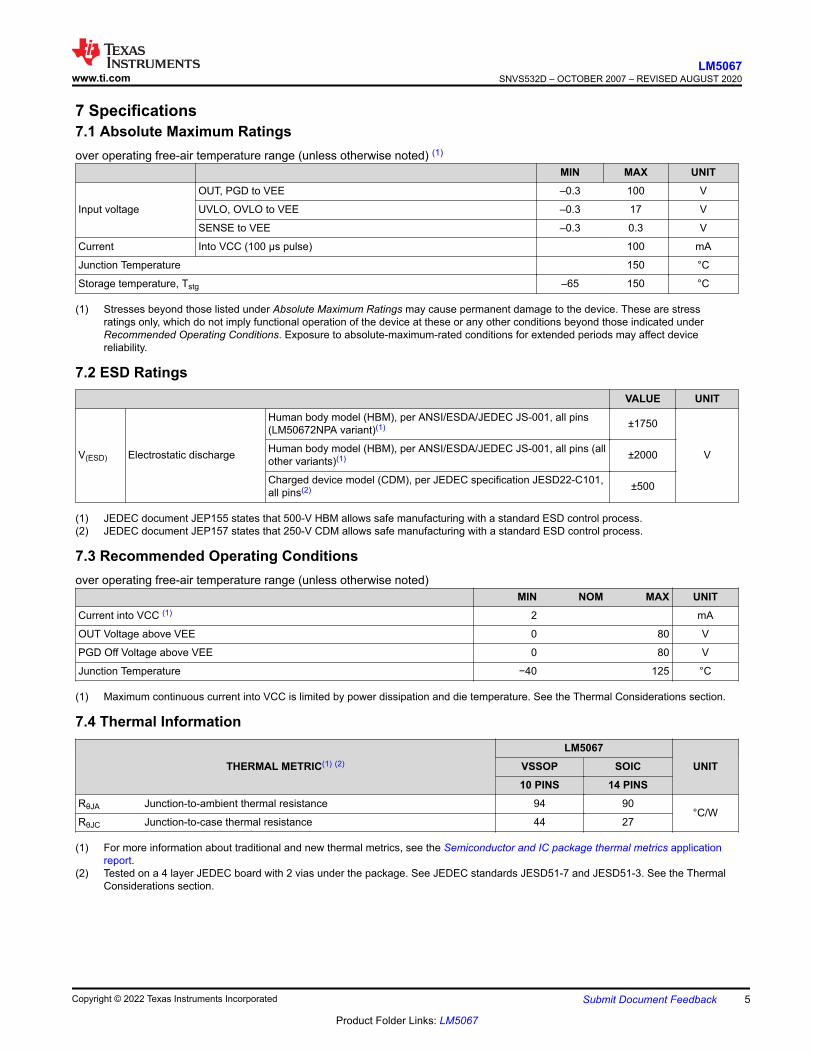
7 Specifications7.1 Absolute Maximum Ratingsover operating free-air temperature range (unless otherwise noted) (1)
MIN MAX UNIT
Input voltage
OUT, PGD to VEE –0.3 100 V
UVLO, OVLO to VEE –0.3 17 V
SENSE to VEE –0.3 0.3 V
Current Into VCC (100 µs pulse) 100 mA
Junction Temperature 150 °C
Storage temperature, Tstg –65 150 °C
(1) Stresses beyond those listed under Absolute Maximum Ratings may cause permanent damage to the device. These are stress ratings only, which do not imply functional operation of the device at these or any other conditions beyond those indicated under Recommended Operating Conditions. Exposure to absolute-maximum-rated conditions for extended periods may affect device reliability.
7.2 ESD RatingsVALUE UNIT
V(ESD) Electrostatic discharge
Human body model (HBM), per ANSI/ESDA/JEDEC JS-001, all pins (LM50672NPA variant)(1) ±1750
VHuman body model (HBM), per ANSI/ESDA/JEDEC JS-001, all pins (all other variants)(1) ±2000
Charged device model (CDM), per JEDEC specification JESD22-C101, all pins(2) ±500
(1) JEDEC document JEP155 states that 500-V HBM allows safe manufacturing with a standard ESD control process.(2) JEDEC document JEP157 states that 250-V CDM allows safe manufacturing with a standard ESD control process.
7.3 Recommended Operating Conditionsover operating free-air temperature range (unless otherwise noted)
MIN NOM MAX UNITCurrent into VCC (1) 2 mA
OUT Voltage above VEE 0 80 V
PGD Off Voltage above VEE 0 80 V
Junction Temperature −40 125 °C
(1) Maximum continuous current into VCC is limited by power dissipation and die temperature. See the Thermal Considerations section.
7.4 Thermal Information
THERMAL METRIC(1) (2)
LM5067UNITVSSOP SOIC
10 PINS 14 PINSRθJA Junction-to-ambient thermal resistance 94 90
°C/WRθJC Junction-to-case thermal resistance 44 27
(1) For more information about traditional and new thermal metrics, see the Semiconductor and IC package thermal metrics application report.
(2) Tested on a 4 layer JEDEC board with 2 vias under the package. See JEDEC standards JESD51-7 and JESD51-3. See the Thermal Considerations section.
www.ti.comLM5067
SNVS532D – OCTOBER 2007 – REVISED AUGUST 2020
Copyright © 2022 Texas Instruments Incorporated Submit Document Feedback 5
Product Folder Links: LM5067
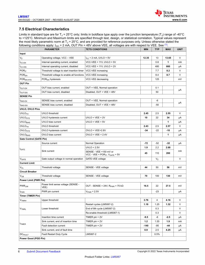
7.5 Electrical CharacteristicsLimits in standard type are for TJ = 25°C only; limits in boldface type apply over the junction temperature (TJ) range of -40°C to +125°C. Minimum and Maximum limits are specified through test, design, or statistical correlation. Typical values represent the most likely parametric norm at TJ = 25°C, and are provided for reference purposes only. Unless otherwise stated the following conditions apply: ICC = 2 mA, OUT Pin = 48V above VEE, all voltages are with respect to VEE. See (1).
PARAMETER TETS CONDITIONS MIN TYP MAX UNIT
Input
VZ Operating voltage, VCC – VEE ICC = 2 mA, UVLO = 5V 12.35 13 13.65 V
ICC-EN Internal operating current, enabled VCC-VEE = 11V, UVLO = 5V 0.8 1 mA
ICC-DIS Internal operating current, disabled VCC-VEE = 11V, UVLO = 2V 480 660 µA
PORIT Threshold voltage to start insertion timer VCC-VEE increasing 7.7 8.2 V
POREN Threshold voltage to enable all functions VCC-VEE increasing 8.4 8.7 V
POREN-HYS POREN hysteresis VCC-VEE decreasing 125 mV
OUT Pin
IOUT-EN OUT bias current, enabled OUT = VEE, Normal operation 0.1µA
IOUT-DIS OUT bias current, disabled Disabled, OUT = VEE + 48V 50
SENSE Pin
ISNS-EN SENSE bias current, enabled OUT = VEE, Normal operation -6µA
ISNS-DIS SENSE bias current, disabled Disabled, OUT = VEE + 48V -50
UVLO, OVLO Pins
UVLOTH UVLO threshold 2.45 2.5 2.55 V
UVLOHYS UVLO hysteresis current UVLO = VEE + 2V 10 22 34 µA
UVLOBIAS UVLO bias current UVLO = VEE + 5V 1 µA
OVLOTH OVLO threshold 2.43 2.5 2.57 V
OVLOHYS OVLO hysteresis current OVLO = VEE+2.8V -34 -22 -10 µA
OVLOBIAS OVLO bias current OVLO = VEE + 2.4V 1 µA
Gate Control (GATE Pin)
IGATE
Source current Normal Operation -72 -52 -32 µA
Sink currentUVLO < 2.5V 1.9 2.2 2.68
mASENSE - VEE =150 mV orVCC - VEE < PORIT, VGATE = 5V 45 110 200
VGATE Gate output voltage in normal operation GATE-VEE voltage VZ V
Current Limit
VCL Threshold voltage SENSE - VEE voltage 44 50 56 mV
Circuit Breaker
VCB Threshold voltage SENSE - VEE voltage 70 100 130 mV
Power Limit (PWR Pin)
PWRLIMPower limit sense voltage (SENSE - VEE) OUT - SENSE = 24V, RPWR = 75 kΩ 16.5 22 27.5 mV
IPWR PWR pin current VPWR = 2.5V -23 µA
Timer (TIMER Pin)
VTMRH Upper threshold 3.76 4 4.16 V
VTMRL Lower threshold
Restart cycles (LM5067-2) 1.18 1.25 1.32 V
End of 8th cycle (LM5067-2) 0.3 V
Re-enable threshold (LM5067-1) 0.3 V
ITIMER
Insertion time current TIMER pin = 2V -9.5 -6 -2.5 µA
Sink current, end of insertion time TIMER pin = 2V 1.2 1.55 1.9 mA
Fault detection current TIMER pin = 2V -140 -95 -44 µA
Sink current, end of fault time 0.9 2.5 4.25 µA
DCFAULT Fault Restart Duty Cycle LM5067-2 0.5%
Power Good (PGD Pin)
LM5067SNVS532D – OCTOBER 2007 – REVISED AUGUST 2020 www.ti.com
6 Submit Document Feedback Copyright © 2022 Texas Instruments Incorporated
Product Folder Links: LM5067
7.5 Electrical Characteristics (continued)Limits in standard type are for TJ = 25°C only; limits in boldface type apply over the junction temperature (TJ) range of -40°C to +125°C. Minimum and Maximum limits are specified through test, design, or statistical correlation. Typical values represent the most likely parametric norm at TJ = 25°C, and are provided for reference purposes only. Unless otherwise stated the following conditions apply: ICC = 2 mA, OUT Pin = 48V above VEE, all voltages are with respect to VEE. See (1).
PARAMETER TETS CONDITIONS MIN TYP MAX UNIT
PGDTH Threshold measured at OUT - SENSEDecreasing 1.162 1.23 1.285 V
Increasing, relative to decreasing threshold 1.143 1.25 1.325
PGDVOL Output low voltage ISINK = 2 mA 60 150 mV
PGDIOH Off leakage current VPGD = 80V 5 µA
(1) Current out of a pin is indicated as a negative value.
7.6 Switching Characteristicsover operating free-air temperature range (unless otherwise noted)
PARAMETER TEST CONDITIONS MIN TYP MAX UNITUVLO, OVLO Pins
UVLODEL UVLO hysteresis currentDelay to GATE high 26 µs
Delay to GATE low 12 µs
OVLODEL OVLO delayDelay to GATE high 26 µs
Delay to GATE low 12 µs
Current Limit
tCL Response time SENSE - VEE stepped from 0 mV to 80 mV 25 µs
Circuit Breaker
tCB Response time SENSE - VEE stepped from 0 mV to 150 mV, time to GATE low, no load 0.65 1.0 µs
Timer (TIMER Pin)tFAULT Fault to GATE low delay TIMER pin reaches 4.0V 15 µs
www.ti.comLM5067
SNVS532D – OCTOBER 2007 – REVISED AUGUST 2020
Copyright © 2022 Texas Instruments Incorporated Submit Document Feedback 7
Product Folder Links: LM5067
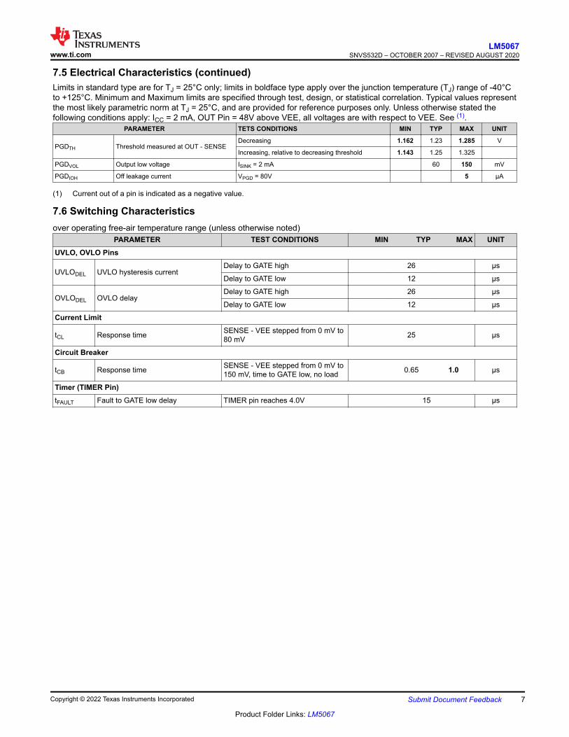
7.7 Typical CharacteristicsUnless otherwise specified the following conditions apply: TJ = 25°C.
Figure 7-1. ICC vs Operating Voltage - Disabled Figure 7-2. ICC vs Operating Voltage - Enabled
Figure 7-3. Operating Voltage vs ICC Figure 7-4. SENSE Pin Current vs System Voltage
Figure 7-5. OUT Pin Current vs System Voltage Figure 7-6. GATE Source Current vs Operating Voltage
LM5067SNVS532D – OCTOBER 2007 – REVISED AUGUST 2020 www.ti.com
8 Submit Document Feedback Copyright © 2022 Texas Instruments Incorporated
Product Folder Links: LM5067
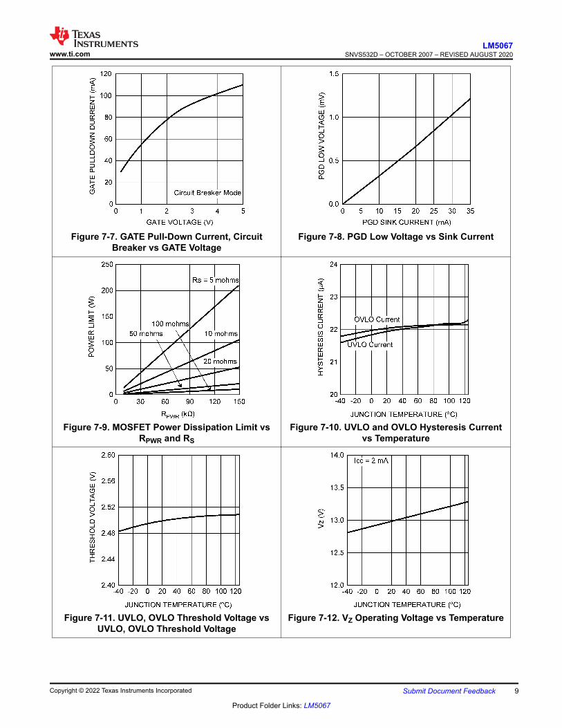
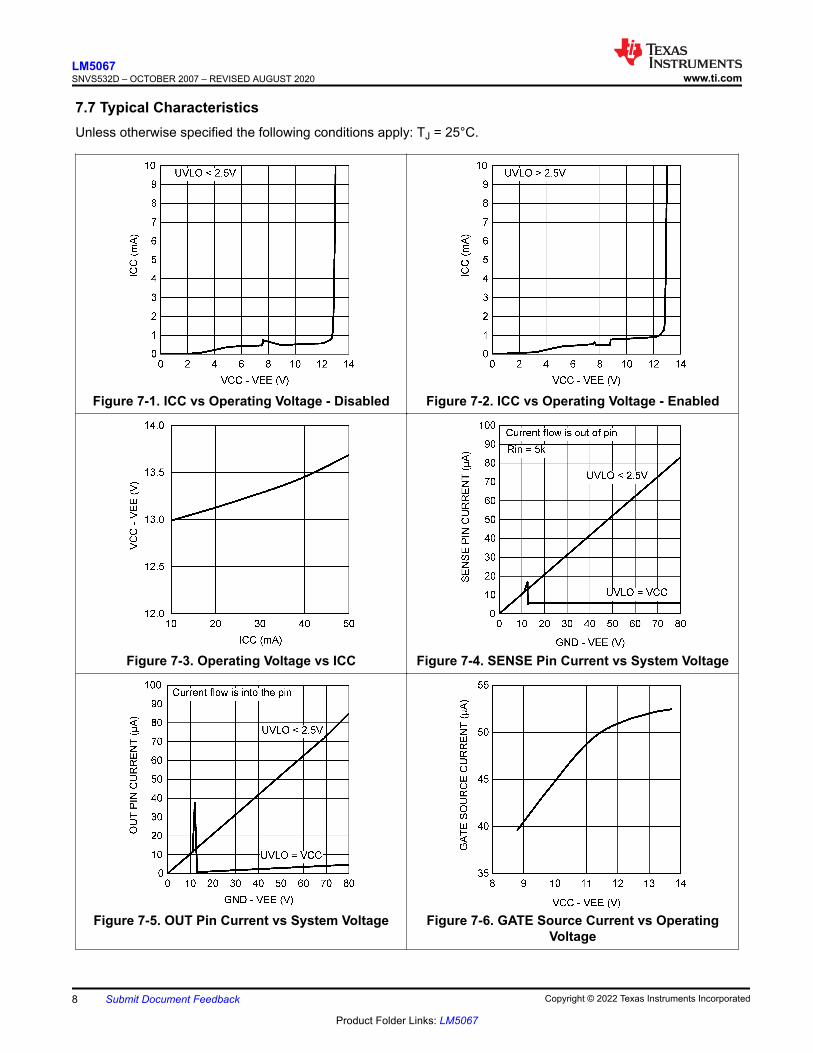
Figure 7-7. GATE Pull-Down Current, Circuit Breaker vs GATE Voltage
Figure 7-8. PGD Low Voltage vs Sink Current
Figure 7-9. MOSFET Power Dissipation Limit vs RPWR and RS
Figure 7-10. UVLO and OVLO Hysteresis Current vs Temperature
Figure 7-11. UVLO, OVLO Threshold Voltage vs UVLO, OVLO Threshold Voltage
Figure 7-12. VZ Operating Voltage vs Temperature
www.ti.comLM5067
SNVS532D – OCTOBER 2007 – REVISED AUGUST 2020
Copyright © 2022 Texas Instruments Incorporated Submit Document Feedback 9
Product Folder Links: LM5067
Figure 7-13. Current Limit Threshold vs Temperature
Figure 7-14. Circuit Breaker Threshold vs Temperature
-40
SENSE Pin ± VEE PinPO
WE
R L
IMIT
TH
RE
SH
OL
D (
mV
)
22
21
20
19
23
24
25
-20 0 20 40 60 80 100 120
RPWR = 75k, VEE = -24V
JUNCTION TEMPERATURE ( C)°
Figure 7-15. Power Limit Threshold vs Temperature
Figure 7-16. Gate Source Current vs Temperature
Figure 7-17. GATE Pull-Down Current, Circuit Breaker vs Temperature
Figure 7-18. PGD Pin Low Voltage vs Temperature
LM5067SNVS532D – OCTOBER 2007 – REVISED AUGUST 2020 www.ti.com
10 Submit Document Feedback Copyright © 2022 Texas Instruments Incorporated
Product Folder Links: LM5067
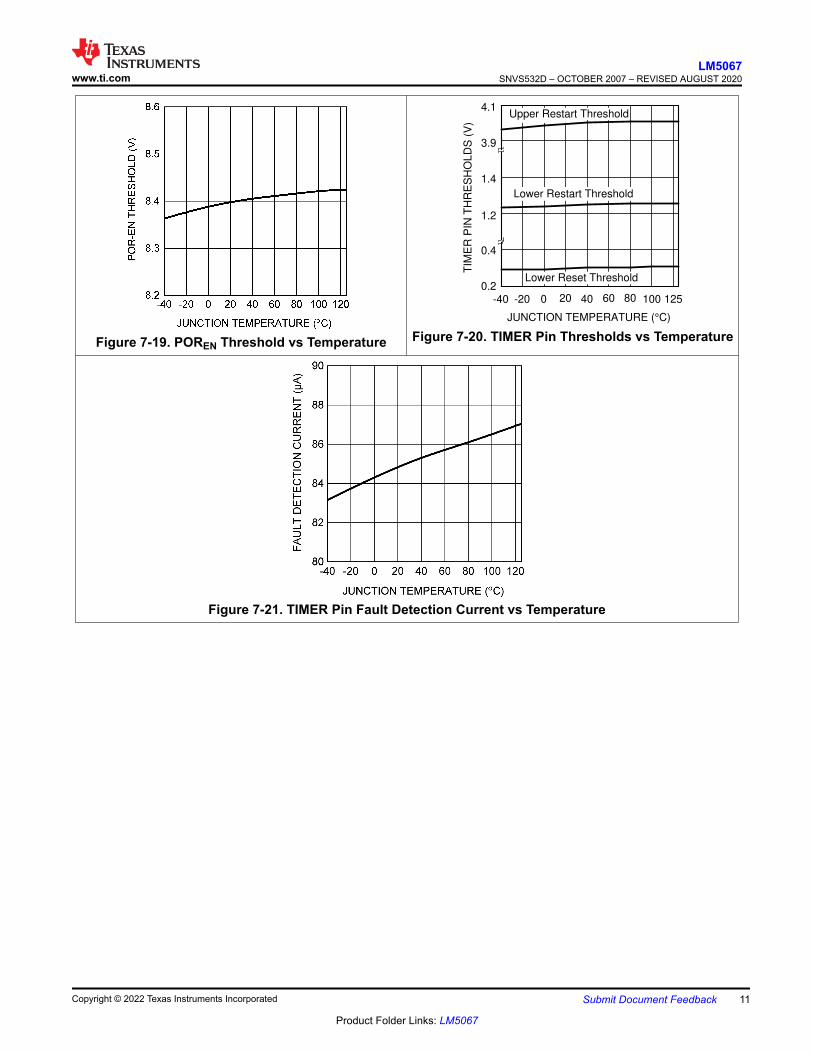
Figure 7-19. POREN Threshold vs Temperature
Upper Restart Threshold
Lower Restart Threshold
Lower Reset Threshold
-40
JUNCTION TEMPERATURE (°C)
-20 0 20 40 60 80 100 125
TIM
ER
PIN
TH
RE
SH
OL
DS
(V
)
1.4
1.2
0.4
0.2
3.9
4.1
Figure 7-20. TIMER Pin Thresholds vs Temperature
Figure 7-21. TIMER Pin Fault Detection Current vs Temperature
www.ti.comLM5067
SNVS532D – OCTOBER 2007 – REVISED AUGUST 2020
Copyright © 2022 Texas Instruments Incorporated Submit Document Feedback 11
Product Folder Links: LM5067
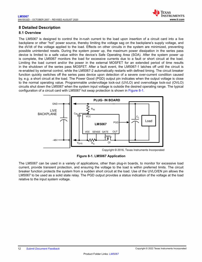
8 Detailed Description8.1 OverviewThe LM5067 is designed to control the in-rush current to the load upon insertion of a circuit card into a live backplane or other “hot” power source, thereby limiting the voltage sag on the backplane’s supply voltage, and the dV/dt of the voltage applied to the load. Effects on other circuits in the system are minimized, preventing possible unintended resets. During the system power up, the maximum power dissipation in the series pass device is limited to a safe value within the device’s Safe Operating Area (SOA). After the system power up is complete, the LM5067 monitors the load for excessive currents due to a fault or short circuit at the load. Limiting the load current and/or the power in the external MOSFET for an extended period of time results in the shutdown of the series pass MOSFET. After a fault event, the LM5067-1 latches off until the circuit is re-enabled by external control, while the LM5067-2 automatically restarts with defined timing. The circuit breaker function quickly switches off the series pass device upon detection of a severe over-current condition caused by, e.g. a short circuit at the load. The Power Good (PGD) output pin indicates when the output voltage is close to the normal operating value. Programmable undervoltage lock-out (UVLO) and overvoltage lock-out (OVLO) circuits shut down the LM5067 when the system input voltage is outside the desired operating range. The typical configuration of a circuit card with LM5067 hot swap protection is shown in Figure 8-1.
Load
VCC
GND
BACKPLANE
PGD
OUT
LIVE
Q1RS
GATESENSEVEE
VSYS
RIN
LM5067
- 48V
PLUG- IN BOARD
CL
CIN
Copyright © 2016, Texas Instruments Incorporated
Figure 8-1. LM5067 Application
The LM5067 can be used in a variety of applications, other than plug-in boards, to monitor for excessive load current, provide transient protection, and ensuring the voltage to the load is within preferred limits. The circuit breaker function protects the system from a sudden short circuit at the load. Use of the UVLO/EN pin allows the LM5067 to be used as a solid state relay. The PGD output provides a status indication of the voltage at the load relative to the input system voltage.
LM5067SNVS532D – OCTOBER 2007 – REVISED AUGUST 2020 www.ti.com
12 Submit Document Feedback Copyright © 2022 Texas Instruments Incorporated
Product Folder Links: LM5067
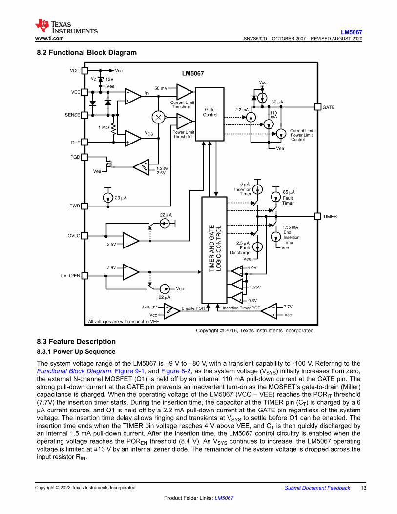
8.2 Functional Block Diagram
GATE
Fault Timer
1.25V
TIMER
1.23V/2.5V
Current Limit Threshold
8.4/8.3V Enable POR
TIM
ER
AN
D G
AT
E
LO
GIC
CO
NT
RO
L
Power Limit Threshold
Gate Control
1.55 mA
EndInsertion
Time
0.3V
7.7V
Vcc
Insertion Timer POR
110mA
VEE
SENSE
OUT
PWR
OVLO
UVLO/EN
InsertionTimer
Fault Discharge
PGD
Vcc
50 mV
2.2 mA
4.0V
2.5V
2.5V
23 PA
22 PA
22 PA
2.5 PA
85 PA
6 PA
52 PA
VDS
1 M:
13V
Vcc
VZ
Vee
VCC
Vee
Vee
Vee
Vee
Vee
Current LimitPower Limit Control
Vcc
LM5067
All voltages are with respect to VEE
ID
Copyright © 2016, Texas Instruments Incorporated
8.3 Feature Description8.3.1 Power Up Sequence
The system voltage range of the LM5067 is –9 V to –80 V, with a transient capability to -100 V. Referring to the Functional Block Diagram, Figure 9-1, and Figure 8-2, as the system voltage (VSYS) initially increases from zero, the external N-channel MOSFET (Q1) is held off by an internal 110 mA pull-down current at the GATE pin. The strong pull-down current at the GATE pin prevents an inadvertent turn-on as the MOSFET’s gate-to-drain (Miller) capacitance is charged. When the operating voltage of the LM5067 (VCC – VEE) reaches the PORIT threshold (7.7V) the insertion timer starts. During the insertion time, the capacitor at the TIMER pin (CT) is charged by a 6 µA current source, and Q1 is held off by a 2.2 mA pull-down current at the GATE pin regardless of the system voltage. The insertion time delay allows ringing and transients at VSYS to settle before Q1 can be enabled. The insertion time ends when the TIMER pin voltage reaches 4 V above VEE, and CT is then quickly discharged by an internal 1.5 mA pull-down current. After the insertion time, the LM5067 control circuitry is enabled when the operating voltage reaches the POREN threshold (8.4 V). As VSYS continues to increase, the LM5067 operating voltage is limited at ≊13 V by an internal zener diode. The remainder of the system voltage is dropped across the input resistor RIN.
www.ti.comLM5067
SNVS532D – OCTOBER 2007 – REVISED AUGUST 2020
Copyright © 2022 Texas Instruments Incorporated Submit Document Feedback 13
Product Folder Links: LM5067
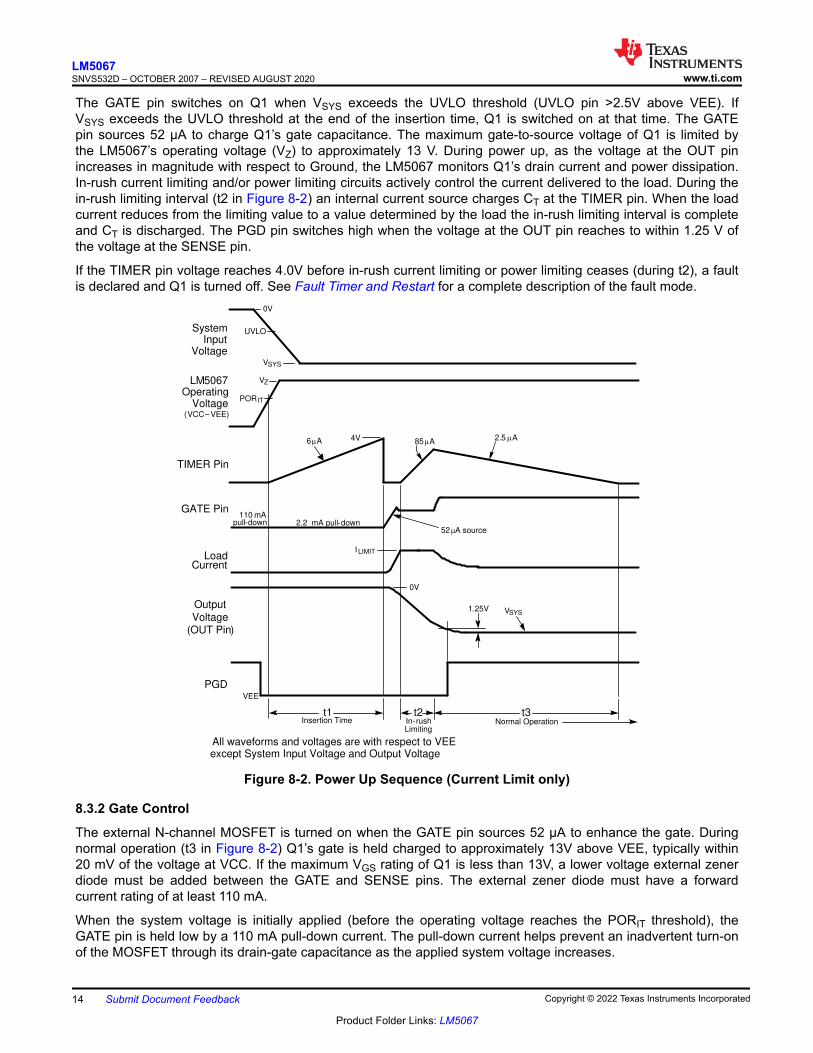
The GATE pin switches on Q1 when VSYS exceeds the UVLO threshold (UVLO pin >2.5V above VEE). If VSYS exceeds the UVLO threshold at the end of the insertion time, Q1 is switched on at that time. The GATE pin sources 52 µA to charge Q1’s gate capacitance. The maximum gate-to-source voltage of Q1 is limited by the LM5067’s operating voltage (VZ) to approximately 13 V. During power up, as the voltage at the OUT pin increases in magnitude with respect to Ground, the LM5067 monitors Q1’s drain current and power dissipation. In-rush current limiting and/or power limiting circuits actively control the current delivered to the load. During the in-rush limiting interval (t2 in Figure 8-2) an internal current source charges CT at the TIMER pin. When the load current reduces from the limiting value to a value determined by the load the in-rush limiting interval is complete and CT is discharged. The PGD pin switches high when the voltage at the OUT pin reaches to within 1.25 V of the voltage at the SENSE pin.
If the TIMER pin voltage reaches 4.0V before in-rush current limiting or power limiting ceases (during t2), a fault is declared and Q1 is turned off. See Fault Timer and Restart for a complete description of the fault mode.
TIMER Pin
Load Current
PGD
UVLO
LimitingNormal Operation
GATE Pin
Insertion Time
Operating Voltage
Output
Voltage
VEE
All waveforms and voltages are with respect to VEE except System Input Voltage and Output Voltage.
2.5 PA85PA
52PA source
4V
0V
2.2 mA pull-down
6 PA
1.25V
ILIMIT
VSYS
pull-down110 mA
0V
VSYS
VZ
PORIT
System Input
Voltage
(VCC ± VEE)
LM5067
(OUT Pin)
t3t2In-rush
t1
Figure 8-2. Power Up Sequence (Current Limit only)
8.3.2 Gate Control
The external N-channel MOSFET is turned on when the GATE pin sources 52 µA to enhance the gate. During normal operation (t3 in Figure 8-2) Q1’s gate is held charged to approximately 13V above VEE, typically within 20 mV of the voltage at VCC. If the maximum VGS rating of Q1 is less than 13V, a lower voltage external zener diode must be added between the GATE and SENSE pins. The external zener diode must have a forward current rating of at least 110 mA.
When the system voltage is initially applied (before the operating voltage reaches the PORIT threshold), the GATE pin is held low by a 110 mA pull-down current. The pull-down current helps prevent an inadvertent turn-on of the MOSFET through its drain-gate capacitance as the applied system voltage increases.
LM5067SNVS532D – OCTOBER 2007 – REVISED AUGUST 2020 www.ti.com
14 Submit Document Feedback Copyright © 2022 Texas Instruments Incorporated
Product Folder Links: LM5067
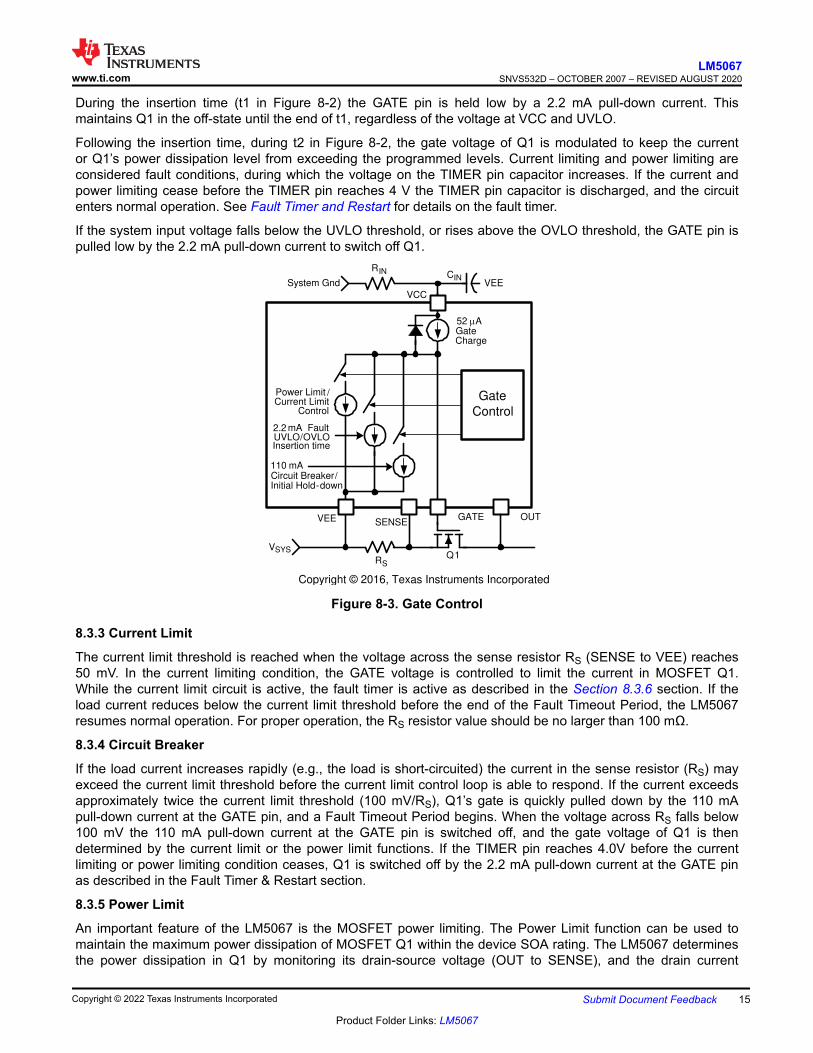
During the insertion time (t1 in Figure 8-2) the GATE pin is held low by a 2.2 mA pull-down current. This maintains Q1 in the off-state until the end of t1, regardless of the voltage at VCC and UVLO.
Following the insertion time, during t2 in Figure 8-2, the gate voltage of Q1 is modulated to keep the current or Q1’s power dissipation level from exceeding the programmed levels. Current limiting and power limiting are considered fault conditions, during which the voltage on the TIMER pin capacitor increases. If the current and power limiting cease before the TIMER pin reaches 4 V the TIMER pin capacitor is discharged, and the circuit enters normal operation. See Fault Timer and Restart for details on the fault timer.
If the system input voltage falls below the UVLO threshold, or rises above the OVLO threshold, the GATE pin is pulled low by the 2.2 mA pull-down current to switch off Q1.
52 PA
GATE
VCC
SENSE
Insertion time
2.2 mA Fault
Current LimitControl
Gate
Control
VEE OUT
VEESystem Gnd
Gate Charge
VSYS
/Power Limit
110 mA
Initial Hold-down
UVLO/OVLO
CINRIN
Q1RS
Circuit Breaker/
Copyright © 2016, Texas Instruments Incorporated
Figure 8-3. Gate Control
8.3.3 Current Limit
The current limit threshold is reached when the voltage across the sense resistor RS (SENSE to VEE) reaches 50 mV. In the current limiting condition, the GATE voltage is controlled to limit the current in MOSFET Q1. While the current limit circuit is active, the fault timer is active as described in the Section 8.3.6 section. If the load current reduces below the current limit threshold before the end of the Fault Timeout Period, the LM5067 resumes normal operation. For proper operation, the RS resistor value should be no larger than 100 mΩ.
8.3.4 Circuit Breaker
If the load current increases rapidly (e.g., the load is short-circuited) the current in the sense resistor (RS) may exceed the current limit threshold before the current limit control loop is able to respond. If the current exceeds approximately twice the current limit threshold (100 mV/RS), Q1’s gate is quickly pulled down by the 110 mA pull-down current at the GATE pin, and a Fault Timeout Period begins. When the voltage across RS falls below 100 mV the 110 mA pull-down current at the GATE pin is switched off, and the gate voltage of Q1 is then determined by the current limit or the power limit functions. If the TIMER pin reaches 4.0V before the current limiting or power limiting condition ceases, Q1 is switched off by the 2.2 mA pull-down current at the GATE pin as described in the Fault Timer & Restart section.
8.3.5 Power Limit
An important feature of the LM5067 is the MOSFET power limiting. The Power Limit function can be used to maintain the maximum power dissipation of MOSFET Q1 within the device SOA rating. The LM5067 determines the power dissipation in Q1 by monitoring its drain-source voltage (OUT to SENSE), and the drain current
www.ti.comLM5067
SNVS532D – OCTOBER 2007 – REVISED AUGUST 2020
Copyright © 2022 Texas Instruments Incorporated Submit Document Feedback 15
Product Folder Links: LM5067
through the sense resistor (SENSE to VEE). The product of the current and voltage is compared to the power limit threshold programmed by the resistor at the PWR pin. If the power dissipation reaches the limiting threshold, the GATE voltage is modulated to reduce the current in Q1, and the fault timer is active as described in the Fault Timer and Restart section.
8.3.6 Fault Timer and Restart
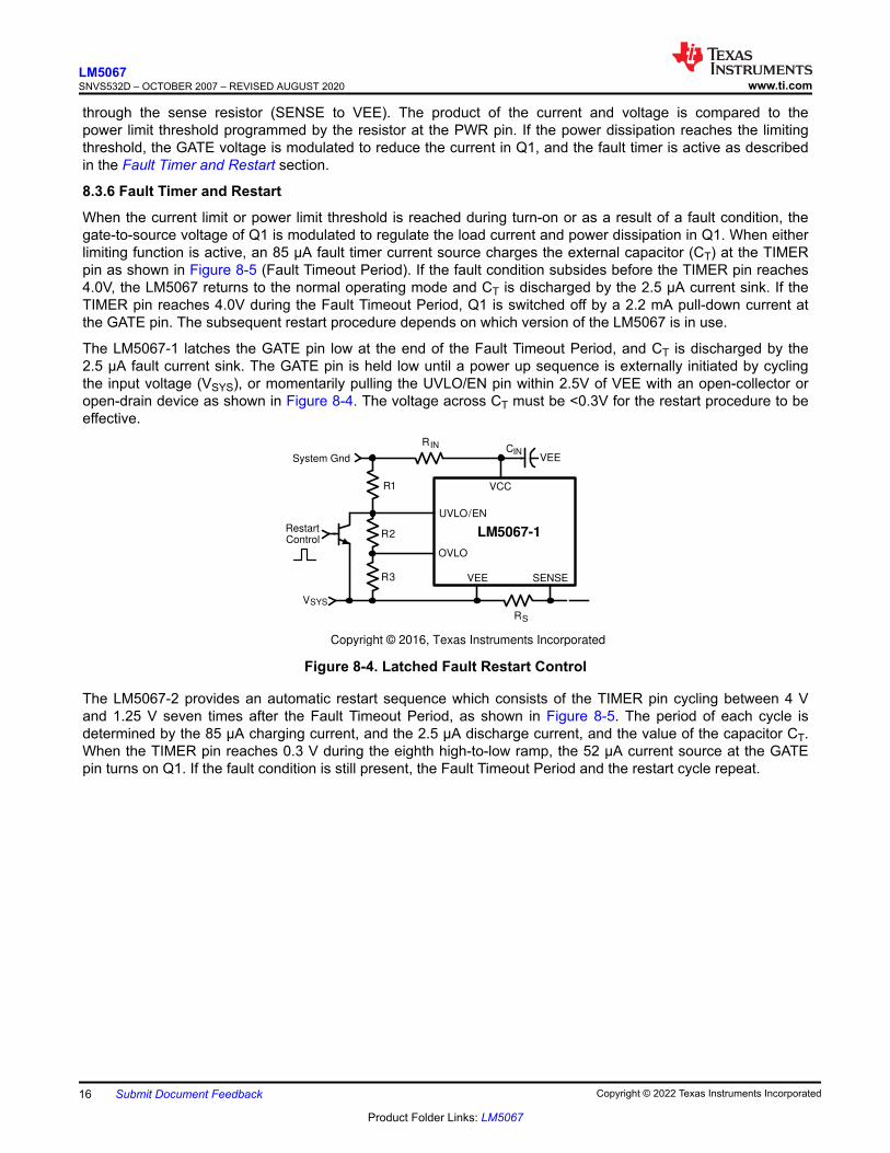
When the current limit or power limit threshold is reached during turn-on or as a result of a fault condition, the gate-to-source voltage of Q1 is modulated to regulate the load current and power dissipation in Q1. When either limiting function is active, an 85 µA fault timer current source charges the external capacitor (CT) at the TIMER pin as shown in Figure 8-5 (Fault Timeout Period). If the fault condition subsides before the TIMER pin reaches 4.0V, the LM5067 returns to the normal operating mode and CT is discharged by the 2.5 µA current sink. If the TIMER pin reaches 4.0V during the Fault Timeout Period, Q1 is switched off by a 2.2 mA pull-down current at the GATE pin. The subsequent restart procedure depends on which version of the LM5067 is in use.
The LM5067-1 latches the GATE pin low at the end of the Fault Timeout Period, and CT is discharged by the 2.5 µA fault current sink. The GATE pin is held low until a power up sequence is externally initiated by cycling the input voltage (VSYS), or momentarily pulling the UVLO/EN pin within 2.5V of VEE with an open-collector or open-drain device as shown in Figure 8-4. The voltage across CT must be <0.3V for the restart procedure to be effective.
RestartControl
VCC
OVLO
VEE
System Gnd VEE
SENSE
VSYS
CINRIN
R1
R2
RS
UVLO/EN
LM5067-1
R3
Copyright © 2016, Texas Instruments Incorporated
Figure 8-4. Latched Fault Restart Control
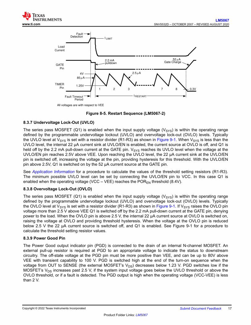
The LM5067-2 provides an automatic restart sequence which consists of the TIMER pin cycling between 4 V and 1.25 V seven times after the Fault Timeout Period, as shown in Figure 8-5. The period of each cycle is determined by the 85 µA charging current, and the 2.5 µA discharge current, and the value of the capacitor CT. When the TIMER pin reaches 0.3 V during the eighth high-to-low ramp, the 52 µA current source at the GATE pin turns on Q1. If the fault condition is still present, the Fault Timeout Period and the restart cycle repeat.
LM5067SNVS532D – OCTOBER 2007 – REVISED AUGUST 2020 www.ti.com
16 Submit Document Feedback Copyright © 2022 Texas Instruments Incorporated
Product Folder Links: LM5067
I LIMIT
Load Current
GATE Pin
TIMER Pin 1 2 3 7 8
2.2 mA pulldown
Fault Timeout Period
0.3V
Fault Detection
t RESTART
1.25V
85 PA
4V
52 PA Gate Charge
All voltages are with respect to VEE
2.5 PA
Figure 8-5. Restart Sequence (LM5067-2)
8.3.7 Undervoltage Lock-Out (UVLO)
The series pass MOSFET (Q1) is enabled when the input supply voltage (VSYS) is within the operating range defined by the programmable undervoltage lockout (UVLO) and overvoltage lock-out (OVLO) levels. Typically the UVLO level at VSYS is set with a resistor divider (R1-R3) as shown in Figure 9-1. When VSYS is less than the UVLO level, the internal 22 µA current sink at UVLO/EN is enabled, the current source at OVLO is off, and Q1 is held off by the 2.2 mA pull-down current at the GATE pin. VSYS reaches its UVLO level when the voltage at the UVLO/EN pin reaches 2.5V above VEE. Upon reaching the UVLO level, the 22 µA current sink at the UVLO/EN pin is switched off, increasing the voltage at the pin, providing hysteresis for this threshold. With the UVLO/EN pin above 2.5V, Q1 is switched on by the 52 µA current source at the GATE pin.
See Application Information for a procedure to calculate the values of the threshold setting resistors (R1-R3). The minimum possible UVLO level can be set by connecting the UVLO/EN pin to VCC. In this case Q1 is enabled when the operating voltage (VCC – VEE) reaches the POREN threshold (8.4V).
8.3.8 Overvoltage Lock-Out (OVLO)
The series pass MOSFET (Q1) is enabled when the input supply voltage (VSYS) is within the operating range defined by the programmable undervoltage lockout (UVLO) and overvoltage lock-out (OVLO) levels. Typically the OVLO level at VSYS is set with a resistor divider (R1-R3) as shown in Figure 9-1. If VSYS raises the OVLO pin voltage more than 2.5 V above VEE Q1 is switched off by the 2.2 mA pull-down current at the GATE pin, denying power to the load. When the OVLO pin is above 2.5 V, the internal 22 µA current source at OVLO is switched on, raising the voltage at OVLO and providing threshold hysteresis. When the voltage at the OVLO pin is reduced below 2.5 V the 22 µA current source is switched off, and Q1 is enabled. See Figure 9-1 for a procedure to calculate the threshold setting resistor values.
8.3.9 Power Good Pin
The Power Good output indicator pin (PGD) is connected to the drain of an internal N-channel MOSFET. An external pull-up resistor is required at PGD to an appropriate voltage to indicate the status to downstream circuitry. The off-state voltage at the PGD pin must be more positive than VEE, and can be up to 80V above VEE with transient capability to 100 V. PGD is switched high at the end of the turn-on sequence when the voltage from OUT to SENSE (the external MOSFET’s VDS) decreases below 1.23 V. PGD switches low if the MOSFET’s VDS increases past 2.5 V, if the system input voltage goes below the UVLO threshold or above the OVLO threshold, or if a fault is detected. The PGD output is high when the operating voltage (VCC-VEE) is less than 2 V.
www.ti.comLM5067
SNVS532D – OCTOBER 2007 – REVISED AUGUST 2020
Copyright © 2022 Texas Instruments Incorporated Submit Document Feedback 17
Product Folder Links: LM5067

8.4 Device Functional Modes8.4.1 Shutdown / Enable Control
Figure 8-6 shows how to use the UVLO/EN pin for remote shutdown and enable control. Taking the UVLO/EN pin below its 2.5V threshold (with respect to VEE) shuts off the load current. Upon releasing the UVLO/EN pin the LM5067 switches on the load current with in-rush current and power limiting. In Figure 8-7 the OVLO pin is used for remote shutdown and enable control. When the external transistor is off, the OVLO pin is above its 2.5 V threshold (with respect to VEE) and the load current is shut off. Turning on the external transistor allows the LM5067 to switch on the load current with in-rush current and power limiting.
ShutdownControl
VCC
OVLO
VEE
System Gnd VEE
SENSE
VSYS
CINRIN
R1
R2
RS
UVLO/EN
LM5067
R3
Copyright © 2016, Texas Instruments Incorporated
Figure 8-6. Shutdown/Enable Using the UVLO/EN Pin
ShutdownControl
VCC
OVLO
VEE
System Gnd VEE
SENSE
VSYS
CINRIN
R3100k
R1
R2
RS
UVLO/EN
LM5067
Copyright © 2016, Texas Instruments Incorporated
Figure 8-7. Shutdown/Enable Using the OVLO Pin
LM5067SNVS532D – OCTOBER 2007 – REVISED AUGUST 2020 www.ti.com
18 Submit Document Feedback Copyright © 2022 Texas Instruments Incorporated
Product Folder Links: LM5067
9 Application and ImplementationNote
Information in the following applications sections is not part of the TI component specification, and TI does not warrant its accuracy or completeness. TI’s customers are responsible for determining suitability of components for their purposes, as well as validating and testing their design implementation to confirm system functionality.
9.1 Application InformationThe LM5067 is a hotswap controller which is used to manage inrush current and protect in case of faults.
When designing a hotswap, three key scenarios should be considered:
• Start-up• Output of a hotswap is shorted to ground when the hotswap is on. This is often referred to as a hot-short.• Powering-up a board when the output and ground are shorted. This is usually called a start-into-short.
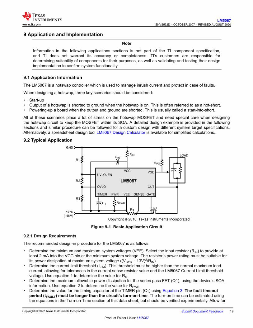
All of these scenarios place a lot of stress on the hotswap MOSFET and need special care when designing the hotswap circuit to keep the MOSFET within its SOA. A detailed design example is provided in the following sections and similar procedure can be followed for a custom design with different system target specifications. Alternatively, a spreadsheet design tool LM5067 Design Calculator is available for simplified calculations..
9.2 Typical ApplicationGND
LOAD
VCC
VEE SENSETIMER GATE
OVLO
PGD
LM5067
PWR
OUT
RPG
RINCIN
Q1RS
RPWRCT
R1
R2
R3
VSYS
(- 48V)
UVLO / EN
Copyright © 2016, Texas Instruments Incorporated
Figure 9-1. Basic Application Circuit
9.2.1 Design Requirements
The recommended design-in procedure for the LM5067 is as follows:
• Determine the minimum and maximum system voltages (VEE). Select the input resistor (RIN) to provide at least 2 mA into the VCC pin at the minimum system voltage. The resistor’s power rating must be suitable for its power dissipation at maximum system voltage ((VSYS – 13V)2/RIN).
• Determine the current limit threshold (ILIM). This threshold must be higher than the normal maximum load current, allowing for tolerances in the current sense resistor value and the LM5067 Current Limit threshold voltage. Use equation 1 to determine the value for RS.
• Determine the maximum allowable power dissipation for the series pass FET (Q1), using the device’s SOA information. Use equation 2 to determine the value for RPWR.
• Determine the value for the timing capacitor at the TIMER pin (CT) using Equation 3. The fault timeout period (tFAULT) must be longer than the circuit’s turn-on-time. The turn-on time can be estimated using the equations in the Turn-on Time section of this data sheet, but should be verified experimentally. Allow for
www.ti.comLM5067
SNVS532D – OCTOBER 2007 – REVISED AUGUST 2020
Copyright © 2022 Texas Instruments Incorporated Submit Document Feedback 19
Product Folder Links: LM5067
tolerances in the values of the external capacitors, sense resistor, and the LM5067 Electrical Characteristics for the TIMER pin, current limit and power limt. Review the resulting insertion time, and the restart timing if the LM5067-2 is used.
• Choose option A, B, C, or D from the UVLO, OVLO section of the Application Information for setting the UVLO and OVLO thresholds and hysteresis. Use the procedure in the appropriate option to determine the resistor values at the UVLO and OVLO pins.
• Choose the appropriate voltage, and pull-up resistor, for the Power Good output.
9.2.2 Detailed Design Procedure9.2.2.1 RIN, CIN
The LM5067 operating voltage is determined by an internal 13 V shunt regulator which receives its current from the system voltage via RIN. When the system voltage exceeds 13V, the LM5067 operating voltage (VCC – VEE) is between VEE and VEE + 13 V. The remainder of the system voltage is dropped across the input resistor RIN, which must be selected to pass at least 2 mA into the LM5067 at the minimum system voltage. The resistor’s power rating must be selected based on the power dissipation at maximum system voltage, calculated from:
PRIN = (VSYS(max) – 13 V)2/RIN (1)
9.2.2.2 Current Limit, RS
The LM5067 monitors the current in the external MOSFET (Q1) by measuring the voltage across the sense resistor (RS), connected from SENSE to VEE. The required resistor value is calculated from:
SLIM
50 mVR =
I (2)
where
• ILIM is the desired current limit threshold
When the voltage across RS reaches 50 mV, the current limit circuit modulates the gate of Q1 to regulate the current at ILIM. While the current limiting circuit is active, the fault timer is active as described in the Fault Timer and Restart section. For proper operation, RS must be no larger than 100 mΩ.
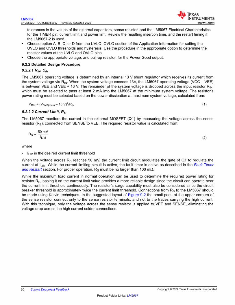
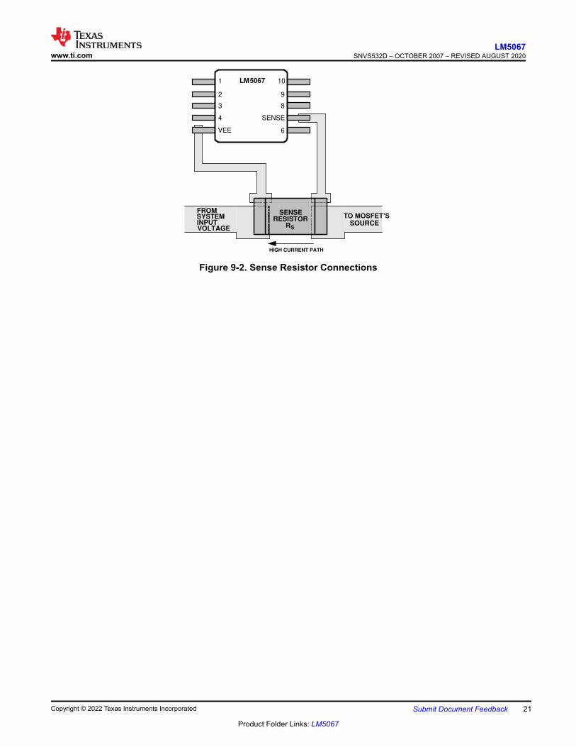
While the maximum load current in normal operation can be used to determine the required power rating for resistor RS, basing it on the current limit value provides a more reliable design since the circuit can operate near the current limit threshold continuously. The resistor’s surge capability must also be considered since the circuit breaker threshold is approximately twice the current limit threshold. Connections from RS to the LM5067 should be made using Kelvin techniques. In the suggested layout of Figure 9-2 the small pads at the upper corners of the sense resistor connect only to the sense resistor terminals, and not to the traces carrying the high current. With this technique, only the voltage across the sense resistor is applied to VEE and SENSE, eliminating the voltage drop across the high current solder connections.
LM5067SNVS532D – OCTOBER 2007 – REVISED AUGUST 2020 www.ti.com
20 Submit Document Feedback Copyright © 2022 Texas Instruments Incorporated
Product Folder Links: LM5067
72026)(7¶6SOURCE
HIGH CURRENT PATH
1
2
3
4
10
9
8
6VEE
SENSE
SENSE
RESISTOR
FROM SYSTEM INPUT VOLTAGE
LM5067
SR
Figure 9-2. Sense Resistor Connections
www.ti.comLM5067
SNVS532D – OCTOBER 2007 – REVISED AUGUST 2020
Copyright © 2022 Texas Instruments Incorporated Submit Document Feedback 21
Product Folder Links: LM5067
9.2.2.3 Power Limit Threshold
The LM5067 determines the power dissipation in the external MOSFET (Q1) by monitoring the drain current (the current in RS), and the VDS of Q1 (OUT to SENSE pins). The resistor at the PWR pin (RPWR) sets the maximum power dissipation for Q1, and is calculated from the following equation:
RPWR = 1.42 x 10⁵ x RS x PFET(LIM) (3)
where
• PFET(LIM) is the desired power limit threshold for Q1• RS is the current sense resistor described in the Current Limit section
For example, if RS is 10 mΩ, and the desired power limit threshold is 60W, RPWR calculates to 85.2 kΩ. If the Q1 power dissipation reaches the power limit threshold, the Q1 gate is modulated to control the load current, keeping Q1 power from exceeding the threshold. For proper operation of the power limiting feature, RPWR must be ≤150 kΩ. While the power limiting circuit is active, the fault timer is active as described in the Fault Timer and Restart section. Typically, power limit is reached during startup, or when the VDS of Q1 increases due to a severe overload or short circuit.
The programmed maximum power dissipation should have a reasonable margin relative to the maximum power defined by the SOA chart if the LM5067-2 is used since the FET will be repeatedly stressed during fault restart cycles. The FET manufacturer should be consulted for guidelines. The PWR pin can be left open if the application does not require use of the power limit function.
9.2.2.4 Turn-On Time
The output turn-on time depends on whether the LM5067 operates in current limit only, or in both power limit and current limit, during turn-on.
9.2.2.4.1 Turn-on With Current Limit Only
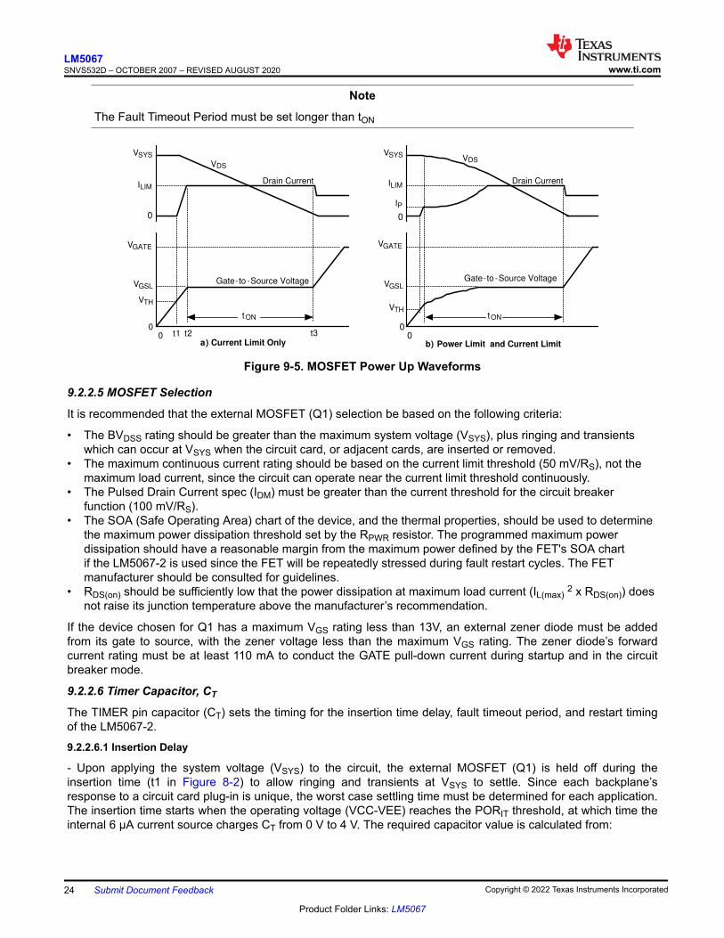
If the current limit threshold is less than the current defined by the power limit threshold at maximum VDS the circuit operates only at the current limit threshold during turn-on. Referring to Figure 9-5a, as the drain current reaches ILIM, the gate-to-source voltage is controlled at VGSL to maintain the current at ILIM. As the output voltage reaches its final value (VDS ≊ 0 V) the drain current reduces to the value defined by the load, and the gate is charged to approximately 13 V (VGATE). The time for the OUT pin voltage to transition from zero volts to VSYS is equal to:
SYS LON
LIM
V x Ct =
I (4)
where
• CL is the load capacitance
For example, if VSYS = –48 V, CL = 1000 µF, and ILIM = 1 A, tON calculates to 48 ms. The maximum instantaneous power dissipated in the MOSFET is 48W. This calculation assumes the time from t1 to t2 in Figure 9-5a is small compared to tON, and the load does not draw any current until after the output voltage has reached its final value, and PGD switches high (Figure 9-3).
LM5067SNVS532D – OCTOBER 2007 – REVISED AUGUST 2020 www.ti.com
22 Submit Document Feedback Copyright © 2022 Texas Instruments Incorporated
Product Folder Links: LM5067
VCC
PGD
OUT
GND
GATESENSEVEE
VEE
LM5067
CINRIN
RS
VSYS
RL
CL
Q1
Copyright © 2016, Texas Instruments Incorporated
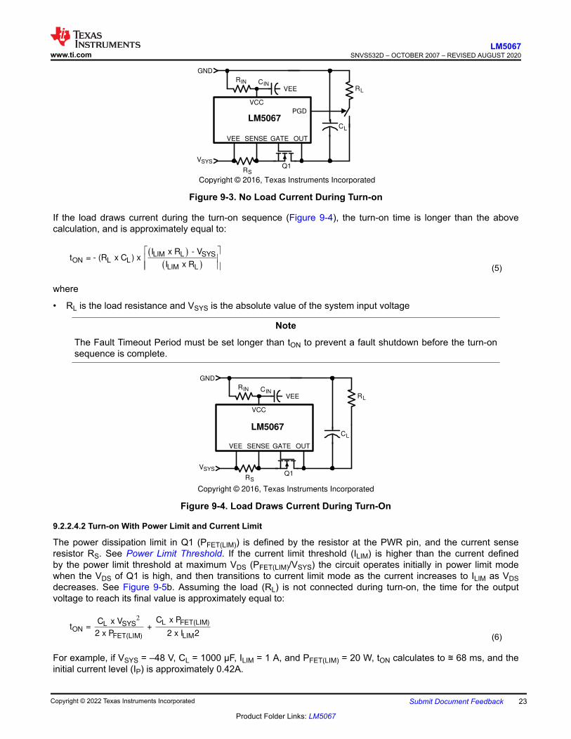
Figure 9-3. No Load Current During Turn-on
If the load draws current during the turn-on sequence (Figure 9-4), the turn-on time is longer than the above calculation, and is approximately equal to:
ª º« »« »¬ ¼
LIM L SYSON L L
LIM L
I x R - Vt = - (R x C ) x
I x R (5)
where
• RL is the load resistance and VSYS is the absolute value of the system input voltage
Note
The Fault Timeout Period must be set longer than tON to prevent a fault shutdown before the turn-on sequence is complete.
VCC
OUT
GND
GATESENSEVEE
VEE
LM5067
CINRIN
RS
VSYS
RL
CL
Q1
Copyright © 2016, Texas Instruments Incorporated
Figure 9-4. Load Draws Current During Turn-On
9.2.2.4.2 Turn-on With Power Limit and Current Limit
The power dissipation limit in Q1 (PFET(LIM)) is defined by the resistor at the PWR pin, and the current sense resistor RS. See Power Limit Threshold. If the current limit threshold (ILIM) is higher than the current defined by the power limit threshold at maximum VDS (PFET(LIM)/VSYS) the circuit operates initially in power limit mode when the VDS of Q1 is high, and then transitions to current limit mode as the current increases to ILIM as VDS decreases. See Figure 9-5b. Assuming the load (RL) is not connected during turn-on, the time for the output voltage to reach its final value is approximately equal to:
2L FET(LIM)L SYS
ONFET(LIM) LIM
C x PC x Vt = +
2 x P 2 x I 2 (6)
For example, if VSYS = –48 V, CL = 1000 µF, ILIM = 1 A, and PFET(LIM) = 20 W, tON calculates to ≊ 68 ms, and the initial current level (IP) is approximately 0.42A.
www.ti.comLM5067
SNVS532D – OCTOBER 2007 – REVISED AUGUST 2020
Copyright © 2022 Texas Instruments Incorporated Submit Document Feedback 23
Product Folder Links: LM5067
Note
The Fault Timeout Period must be set longer than tON
0
0
Drain Current
0t10
0 t2 t3a) Current Limit Only
VSYS VDS
ILIM
IP
VGATE
VGSL
VTHtON
Source Voltage-toGate-
b) Power Limit and Current Limit
VDS
Drain Current
tON
0
VSYS
ILIM
VGATE
VGSL
VTH
Source Voltage-toGate-
Figure 9-5. MOSFET Power Up Waveforms
9.2.2.5 MOSFET Selection
It is recommended that the external MOSFET (Q1) selection be based on the following criteria:
• The BVDSS rating should be greater than the maximum system voltage (VSYS), plus ringing and transients which can occur at VSYS when the circuit card, or adjacent cards, are inserted or removed.
• The maximum continuous current rating should be based on the current limit threshold (50 mV/RS), not the maximum load current, since the circuit can operate near the current limit threshold continuously.
• The Pulsed Drain Current spec (IDM) must be greater than the current threshold for the circuit breaker function (100 mV/RS).
• The SOA (Safe Operating Area) chart of the device, and the thermal properties, should be used to determine the maximum power dissipation threshold set by the RPWR resistor. The programmed maximum power dissipation should have a reasonable margin from the maximum power defined by the FET's SOA chart if the LM5067-2 is used since the FET will be repeatedly stressed during fault restart cycles. The FET manufacturer should be consulted for guidelines.
• RDS(on) should be sufficiently low that the power dissipation at maximum load current (IL(max) 2 x RDS(on)) does not raise its junction temperature above the manufacturer’s recommendation.
If the device chosen for Q1 has a maximum VGS rating less than 13V, an external zener diode must be added from its gate to source, with the zener voltage less than the maximum VGS rating. The zener diode’s forward current rating must be at least 110 mA to conduct the GATE pull-down current during startup and in the circuit breaker mode.
9.2.2.6 Timer Capacitor, CT
The TIMER pin capacitor (CT) sets the timing for the insertion time delay, fault timeout period, and restart timing of the LM5067-2.
9.2.2.6.1 Insertion Delay
- Upon applying the system voltage (VSYS) to the circuit, the external MOSFET (Q1) is held off during the insertion time (t1 in Figure 8-2) to allow ringing and transients at VSYS to settle. Since each backplane’s response to a circuit card plug-in is unique, the worst case settling time must be determined for each application. The insertion time starts when the operating voltage (VCC-VEE) reaches the PORIT threshold, at which time the internal 6 µA current source charges CT from 0 V to 4 V. The required capacitor value is calculated from:
LM5067SNVS532D – OCTOBER 2007 – REVISED AUGUST 2020 www.ti.com
24 Submit Document Feedback Copyright © 2022 Texas Instruments Incorporated
Product Folder Links: LM5067
6PT
t1 x 6 AC = = t1 x 1.5 x 10
4 V (7)
where
• t1 is the desired insertion delay
For example, if the desired insertion delay is 250 ms, CT calculates to 0.38 µF. At the end of the insertion delay, CT is quickly discharged by a 1.5 mA current sink.
9.2.2.6.2 Fault Timeout Period
- During turn-on of the output voltage, or upon detection of a fault condition where the current limit and/or power limit circuits regulate the current through Q1, CT is charged by the fault timer current source (85 µA). The Fault Timeout Period is the time required for the TIMER pin voltage to reach 4.0V above VEE, at which time Q1 is switched off. The required capacitor value for the desired Fault Timeout Period tFAULT is calculated from:
5PFAULTT FAULT
t x 85 AC = = t x 2.13 x 10
4 V (8)
For example, if the desired Fault Timeout Period is 16 ms, CT calculates to 0.34 µF. After a fault timeout, if the LM5067-1 is in use, CT must be allowed to discharge to < 0.3 V by the 2.5 µA current sink, after which a power up sequence can be initiated by external circuitry. See Fault Timer and Restart and Latched Fault Restart Control. If the LM5067-2 is in use, after the Fault Timeout Period expires a restart sequence begins as described below (Restart Timing).
Since the LM5067 normally operates in power limit and/or current limit during a power up sequence, the Fault Timeout Period MUST be longer than the time required for the output voltage to reach its final value. See Turn-On Time.
9.2.2.6.3 Restart Timing
If the LM5067-2 is in use, after the Fault Timeout Period described above, CT is discharged by the 2.5 µA current sink to 1.25 V. The TIMER pin then cycles through seven additional charge/discharge cycles between 1.25 V and 4 V as shown in Figure 8-5. The restart time ends when the TIMER pin voltage reaches 0.3 V during the final high-to-low ramp. The restart time, after the Fault Timeout Period, is equal to:
6ª º« »P P P¬ ¼
RESTART T T
7 x 2.75 V 7 x 2.75 V 3.7 Vt = C x + + = C x 9.4 x 10
2.5 A 85 A 2.5 A (9)
For example, if CT = 0.33 µF, tRESTART = 3.1 seconds. At the end of the restart time, Q1 is switched on. If the fault is still present, the fault timeout and restart sequence repeats. The on-time duty cycle of Q1 is approximately 0.5% in this mode.
9.2.2.7 UVLO, OVLO
By programming the UVLO and OVLO thresholds the LM5067 enables the series pass device (Q1) when the input supply voltage (VSYS) is within the desired operational range. If VSYS is below the UVLO threshold, or above the OVLO threshold, Q1 is switched off, denying power to the load. Hysteresis is provided for each threshold.
Note
All voltages are with respect to Vee in the discussions below. Use absolute values in the equations.
www.ti.comLM5067
SNVS532D – OCTOBER 2007 – REVISED AUGUST 2020
Copyright © 2022 Texas Instruments Incorporated Submit Document Feedback 25
Product Folder Links: LM5067

9.2.2.7.1 Option A:
The configuration shown in Figure 9-6 requires three resistors (R1-R3) to set the thresholds.
OVLO
VEE
TIMER AND GATE
LOGIC CONTROL
GND
VEE
To Load
Vee
R2
LM5067
22 PA
CINRIN
VSYS
R1
R3
UVLO/EN
22 PA
Vee
Vee
2.50V
2.50V
VCC
Copyright © 2016, Texas Instruments Incorporated
Figure 9-6. UVLO and OVLO Thresholds Set By R1-R3
The procedure to calculate the resistor values is as follows:• Determine the upper UVLO threshold (VUVH) to enable Q1, and the lower UVLO threshold (VUVL) to disable
Q1.• Determine the upper OVLO threshold (VOVH) to disable Q1.• The lower OVLO threshold (VOVL), to enable Q1, cannot be chosen in advance in this case, but is determined
after the values for R1-R3 are determined. If VOVL must be accurately defined in addition to the other three thresholds, see Option B below.
The resistors are calculated as follows:
P P
UV(HYS)UVH UVL
UVL
OVH UVL
UVL
VV - VR1 = =
22 A 22 A
2.5 V x R1 x VR3 =
V x ( V - 2.5 V)
2.5 V x R1R2 = - R3
V - 2.5 V) (10)
The lower OVLO threshold is calculated from:
ª º§ ·P¨ ¸« »© ¹¬ ¼
OVL2.5 V
V = + (R1 + R2 x - 22 A + 2.5 VR2 (11)
As an example, assume the application requires the following thresholds: VUVH = -36V, VUVL = -32V, VOVH = -60V.
LM5067SNVS532D – OCTOBER 2007 – REVISED AUGUST 2020 www.ti.com
26 Submit Document Feedback Copyright © 2022 Texas Instruments Incorporated
Product Folder Links: LM5067
:P P
::
:: :
36 V - 32 V 4 VR1 = = = 182 k
22 A 22 A
2.5 V x 182 k x 32 VR3 = = 8.23 k
60 V x (32 V - 2.5 V)
2.5 V x 182 kR2 = = -8.23 k = 7.19 k
(32 V - 2.5 V) (12)
The lower OVLO threshold calculates to -55.8V, and the OVLO hysteresis is 4.2V. Note that the OVLO hysteresis is always slightly greater than the UVLO hysteresis in this configuration.
When the R1-R3 resistor values are known, the threshold voltages and hysteresis are calculated from the following:
ª º§ ·P¨ ¸« »© ¹¬ ¼
P
ª º§ ·P¨ ¸« »© ¹¬ ¼
UVH
UVL
UV(HYS)
OVH
OVL
OV(
2.5 VV = 2.5 V + R1 x 22 A +
R2 + R3
2.5 V x (R1 + R2 + R3)V =
R2 + R3
V = R1 x 22 A
2.5 V x (R1 + R2 + R3)V =
R3
2.5 VV = (R1 + R2) x - 22 A + 2.5 V
R3
V PHYS) = (R14 + R2) x 22 A (13)
Note
Ensure the voltages at the UVLO and OVLO pins do not exceed the Absolute Maximum ratings for those pins when the system voltage is at maximum.
9.2.2.7.2 Option B:
If all four thresholds must be accurately defined, the configuration in Figure 9-7 can be used.
www.ti.comLM5067
SNVS532D – OCTOBER 2007 – REVISED AUGUST 2020
Copyright © 2022 Texas Instruments Incorporated Submit Document Feedback 27
Product Folder Links: LM5067
VCC
OVLO
VEE
TIMER AND GATE
LOGIC CONTROL
GND
VEE
To Load
Vee
Vee
Vee
R4
LM5067
22 PA
CINRIN
VSYS
R2
R1
R3
UVLO/EN
2.50V
2.50V
22 PA
Copyright © 2016, Texas Instruments Incorporated
Figure 9-7. Programming the Four Thresholds
The four resistor values are calculated as follows:• Determine the upper UVLO threshold (VUVH) to enable Q1, and the lower UVLO threshold (VUVL) to disable
Q1.
UV(HYS)UVH UVL
UVL
VV - VR1 = =
22 $ $
2.5 V x R1R2 =
(V - 2.5 V) (14)
• Determine the upper OVLO threshold (VOVH) to disable Q1, and the lower OVLO threshold (VOVL) to enable Q1.
OV(HYS)OVH OVL
OVL
VV - VR3 = =
22 $ $
2.5 V x R3R4 =
(V - 2.5 V) (15)
As an example, assume the application requires the following thresholds: VUVH = –22 V, VUVL = –17 V, VOVH = –60 V, and VOVL = –58 V. Therefore VUV(HYS) = 5 V, and VOV(HYS) = 2 V. The resistor values are:
R1 = 227 kΩ, R2 = 39.1 kΩ
R3 = 90.9 kΩ, R4 = 3.95 kΩ
Where the R1-R4 resistor values are known, the threshold voltages and hysteresis are calculated from the following:
LM5067SNVS532D – OCTOBER 2007 – REVISED AUGUST 2020 www.ti.com
28 Submit Document Feedback Copyright © 2022 Texas Instruments Incorporated
Product Folder Links: LM5067
ª º§ ·P¨ ¸« »© ¹¬ ¼
P
ª º§ ·P¨ ¸« »© ¹¬ ¼
P
UVH
UVL
UV(HYS)
OVH
OVL
OV(HYS)
2.5 VV = 2.5 V + R1 x + 22 A
R2
2.5 V x (R1 + R2)V =
R2
V = R1 x 22 A
2.5 V x (R3 + R4)V =
R4
2.5 VV = 2.5 V + R3 x - 22 A
R4
V = R3 x 22 A (16)
Note
Ensure the voltages at the UVLO and OVLO pins do not exceed the Absolute Maximum ratings for those pins when the system voltage is at maximum.
www.ti.comLM5067
SNVS532D – OCTOBER 2007 – REVISED AUGUST 2020
Copyright © 2022 Texas Instruments Incorporated Submit Document Feedback 29
Product Folder Links: LM5067
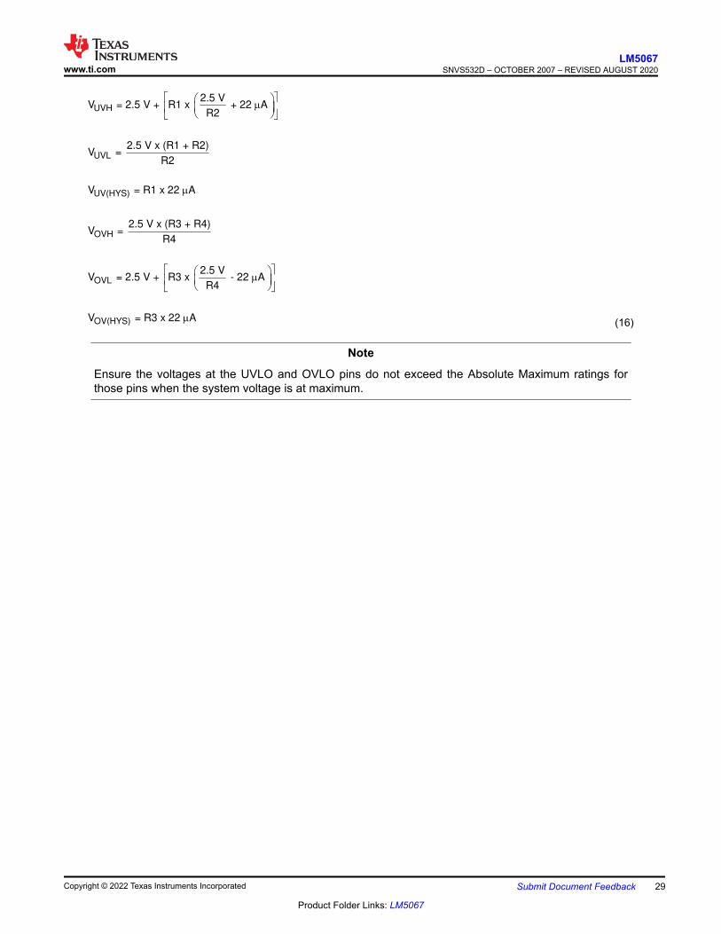
9.2.2.7.3 Option C:
The minimum UVLO level is obtained by connecting the UVLO pin to VCC as shown in Figure 9-8. Q1 is switched on when the operating voltage reaches the POREN threshold (≊8.4V). The OVLO thresholds are set by R3 and R4 using the procedure in Option B.
Note
Ensure the voltage at the OVLO pin does not exceed the Absolute Maximum ratings for that pin when the system voltage is at maximum.
50k
OVLO
VEE
TIMER AND GATE
LOGIC CONTROL
GND
VEE
To Load
Vee
R4
LM5067
22 PA
CINRIN
VSYS
R1
R3
UVLO/EN 2.5V
2.5V
22 PA
VCC
Copyright © 2016, Texas Instruments Incorporated
Figure 9-8. UVLO = POREN
9.2.2.7.4 Option D:
The OVLO function can be disabled by connecting the OVLO pin to VEE. The UVLO thresholds are set as described in Option B or Option C.
9.2.2.8 Thermal Considerations
The LM5067 should be operated so that its junction temperature does not exceed 125°C. The junction temperature is equal to:
TJ = TA + (RθJA x PD) (17)
where
• TA is the ambient temperature• RθJA is the thermal resistance of the LM5067
PD is the power dissipated within the LM5067, calculated from:
PD = 13V x ICC (18)
where
• ICC is the current into the VCC pin (the current through the RIN resistor).
Values for RθJA and RθJC are in Thermal Information.
9.2.2.9 System Considerations
Continued proper operation of the LM5067 hot swap circuit requires capacitance be present on the supply side of the connector into which the hot swap circuit is plugged in, as depicted in Figure 8-1. The capacitor in the “Live Backplane” section is necessary to absorb the transient generated whenever the hot swap circuit shuts off
LM5067SNVS532D – OCTOBER 2007 – REVISED AUGUST 2020 www.ti.com
30 Submit Document Feedback Copyright © 2022 Texas Instruments Incorporated
Product Folder Links: LM5067

the load current. If the capacitance is not present, inductance in the supply lines will generate a voltage transient at shut-off which can exceed the absolute maximum rating of the LM5067, resulting in its destruction.
If the load powered via the LM5067 hot swap circuit has inductive characteristics, a diode is required across the LM5067’s output to provide a recirculating path for the load’s current. Adding the diode prevents possible damage to the LM5067 as the OUT pin will be taken above ground by the inductive load at shutoff. See Figure 9-9
Inductive Load
VCC
GND
BACKPLANE
PGD
OUT
LIVE
Q1 VOUTRS
GATESENSEVEE
VSYS
RIN
LM5067
- 48V
PLUG- IN BOARD
CL
CIN
Copyright © 2016, Texas Instruments Incorporated
Figure 9-9. Output Diode Required for Inductive Loads
9.2.2.9.1 System Considerations During Surge Events
The control MOSFET, Q1, has a body-diode, illustrated in Figure 9-10, where current can freely flow in the reverse direction. The most common cause of a reverse current is a discharge event at the input of the hot-swap circuit when the output capacitance discharges to the input. Normally, reverse current flow presents no issue for hotswap devices during events such as shutdown and minor input power perturbations. However, extreme situations such as high energy lighting surge line disturbances can expose the hot-swap circuit to pulses of ultra fast - high amplitude reverse currents. It is common to observe current amplitudes on the order of 1000 A in these situations. Figure 9-10 illustrates what an extreme input discharge event may look like and how it affects the circuit.
LM5067
VEE
OUT
SENSE GATE
VCC
GND
INPUT
RAILOUTPUT
GND
0 V
VCC - VEE
Reverse
Curent
(IREVERSE)
Region
IREVERSE
+ VRS -
RS Q1
+ VBD -
Input Rail
Discharge
Event
As the input dips, the output capacitor discharges causing a reverse transient current flow.
Z1 D1 COUT
Figure 9-10. Differential Voltage Across Sense Resistor
www.ti.comLM5067
SNVS532D – OCTOBER 2007 – REVISED AUGUST 2020
Copyright © 2022 Texas Instruments Incorporated Submit Document Feedback 31
Product Folder Links: LM5067
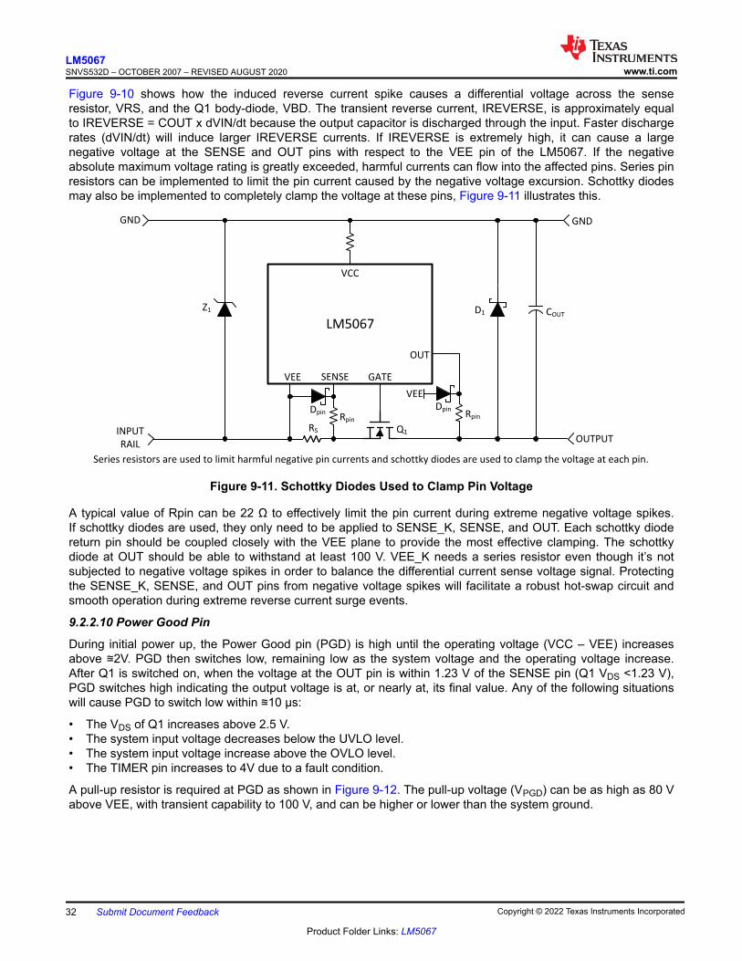
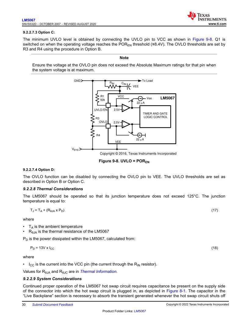
Figure 9-10 shows how the induced reverse current spike causes a differential voltage across the sense resistor, VRS, and the Q1 body-diode, VBD. The transient reverse current, IREVERSE, is approximately equal to IREVERSE = COUT x dVIN/dt because the output capacitor is discharged through the input. Faster discharge rates (dVIN/dt) will induce larger IREVERSE currents. If IREVERSE is extremely high, it can cause a large negative voltage at the SENSE and OUT pins with respect to the VEE pin of the LM5067. If the negative absolute maximum voltage rating is greatly exceeded, harmful currents can flow into the affected pins. Series pin resistors can be implemented to limit the pin current caused by the negative voltage excursion. Schottky diodes may also be implemented to completely clamp the voltage at these pins, Figure 9-11 illustrates this.
LM5067
VEE
OUT
SENSE GATE
VCC
GND
INPUT
RAILOUTPUT
GND
RS Q1
Series resistors are used to limit harmful negative pin currents and schottky diodes are used to clamp the voltage at each pin.
Z1 D1 COUT
VEE
DpinRpin
DpinRpin
Figure 9-11. Schottky Diodes Used to Clamp Pin Voltage
A typical value of Rpin can be 22 Ω to effectively limit the pin current during extreme negative voltage spikes. If schottky diodes are used, they only need to be applied to SENSE_K, SENSE, and OUT. Each schottky diode return pin should be coupled closely with the VEE plane to provide the most effective clamping. The schottky diode at OUT should be able to withstand at least 100 V. VEE_K needs a series resistor even though it’s not subjected to negative voltage spikes in order to balance the differential current sense voltage signal. Protecting the SENSE_K, SENSE, and OUT pins from negative voltage spikes will facilitate a robust hot-swap circuit and smooth operation during extreme reverse current surge events.
9.2.2.10 Power Good Pin
During initial power up, the Power Good pin (PGD) is high until the operating voltage (VCC – VEE) increases above ≊2V. PGD then switches low, remaining low as the system voltage and the operating voltage increase. After Q1 is switched on, when the voltage at the OUT pin is within 1.23 V of the SENSE pin (Q1 VDS <1.23 V), PGD switches high indicating the output voltage is at, or nearly at, its final value. Any of the following situations will cause PGD to switch low within ≊10 µs:
• The VDS of Q1 increases above 2.5 V.• The system input voltage decreases below the UVLO level.• The system input voltage increase above the OVLO level.• The TIMER pin increases to 4V due to a fault condition.
A pull-up resistor is required at PGD as shown in Figure 9-12. The pull-up voltage (VPGD) can be as high as 80 V above VEE, with transient capability to 100 V, and can be higher or lower than the system ground.
LM5067SNVS532D – OCTOBER 2007 – REVISED AUGUST 2020 www.ti.com
32 Submit Document Feedback Copyright © 2022 Texas Instruments Incorporated
Product Folder Links: LM5067
Figure 9-12. Power Good Output
www.ti.comLM5067
SNVS532D – OCTOBER 2007 – REVISED AUGUST 2020
Copyright © 2022 Texas Instruments Incorporated Submit Document Feedback 33
Product Folder Links: LM5067
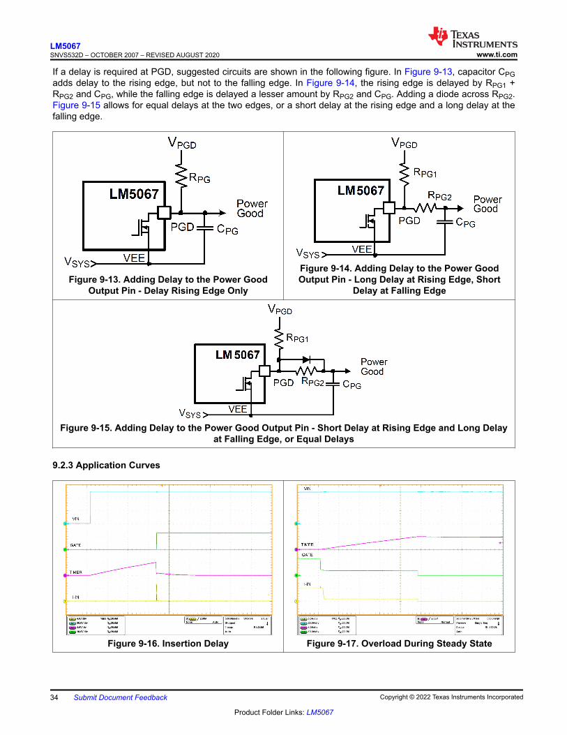
If a delay is required at PGD, suggested circuits are shown in the following figure. In Figure 9-13, capacitor CPG adds delay to the rising edge, but not to the falling edge. In Figure 9-14, the rising edge is delayed by RPG1 + RPG2 and CPG, while the falling edge is delayed a lesser amount by RPG2 and CPG. Adding a diode across RPG2. Figure 9-15 allows for equal delays at the two edges, or a short delay at the rising edge and a long delay at the falling edge.
Figure 9-13. Adding Delay to the Power Good Output Pin - Delay Rising Edge Only
Figure 9-14. Adding Delay to the Power Good Output Pin - Long Delay at Rising Edge, Short
Delay at Falling Edge
Figure 9-15. Adding Delay to the Power Good Output Pin - Short Delay at Rising Edge and Long Delay at Falling Edge, or Equal Delays
9.2.3 Application Curves
Figure 9-16. Insertion Delay Figure 9-17. Overload During Steady State
LM5067SNVS532D – OCTOBER 2007 – REVISED AUGUST 2020 www.ti.com
34 Submit Document Feedback Copyright © 2022 Texas Instruments Incorporated
Product Folder Links: LM5067
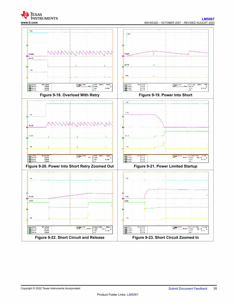
Figure 9-18. Overload With Retry Figure 9-19. Power Into Short
Figure 9-20. Power Into Short Retry Zoomed Out Figure 9-21. Power Limited Startup
Figure 9-22. Short Circuit and Release Figure 9-23. Short Circuit Zoomed In
www.ti.comLM5067
SNVS532D – OCTOBER 2007 – REVISED AUGUST 2020
Copyright © 2022 Texas Instruments Incorporated Submit Document Feedback 35
Product Folder Links: LM5067
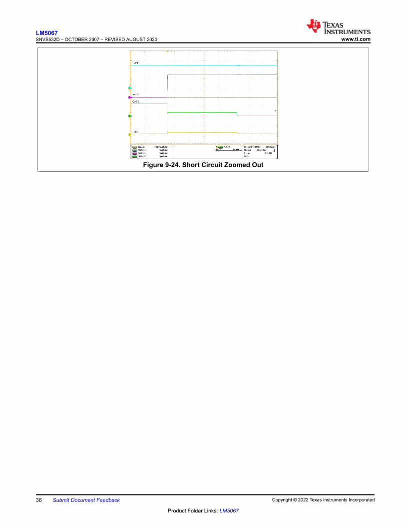
Figure 9-24. Short Circuit Zoomed Out
LM5067SNVS532D – OCTOBER 2007 – REVISED AUGUST 2020 www.ti.com
36 Submit Document Feedback Copyright © 2022 Texas Instruments Incorporated
Product Folder Links: LM5067
10 Power Supply Recommendations10.1 Operating VoltageThe LM5067 operating voltage is the voltage from VCC to VEE. The maximum operating voltage is set by an internal 13V zener diode. With the IC connected as shown in Figure 9-1, the LM5067 controller operates in the voltage range between VEE and VEE+13V. The remainder of the system voltage is dropped across the input resistor RIN, which must be selected to pass at least 2 mA into the LM5067 at the minimum system voltage.
11 Layout11.1 Layout GuidelinesThe following guidelines should be followed when designing the PC board for the LM5067:
• Place the LM5067 close to the board’s input connector to minimize trace inductance from the connector to the FET.
• Place RIN and CIN close to the VCC and VEE pins to keep transients below the Absolute Maximum rating of the LM5067. Transients of several volts can easily occur when the load current is shut off.
• The sense resistor (RS) should be close to the LM5067, and connected to it using the Kelvin techniques shown in Figure 9-2.
• The high current path from the board’s input to the load, and the return path (via Q1), should be parallel and close to each other wherever possible to minimize loop inductance.
• The VEE connection for the various components around the LM5067 should be connected directly to each other, and to the LM5067’s VEE pin, and then connected to the system VEE at one point. Do not connect the various components to each other through the high current VEE track.
• Provide adequate heat sinking for the series pass device (Q1) to help reduce thermal stresses during turn-on and turn-off.
• The board’s edge connector can be designed to shut off the LM5067 as the board is removed, before the supply voltage is disconnected from the LM5067. In Figure 11-1 the voltage at the UVLO/EN pin goes to VEE before VSYS is removed from the LM5067 due to the shorter edge connector pin. When the board is inserted into the edge connector, the system voltage is applied to the LM5067’s VEE and VCC pins before voltage is applied to the UVLO/EN pin.
• If power dissipation within the LM5067 is high, an exposed copper pad should be provided beneath the package, and that pad should be connected to exposed copper on the board’s other side with as many vias as possible. See Thermal Considerations.
www.ti.comLM5067
SNVS532D – OCTOBER 2007 – REVISED AUGUST 2020
Copyright © 2022 Texas Instruments Incorporated Submit Document Feedback 37
Product Folder Links: LM5067
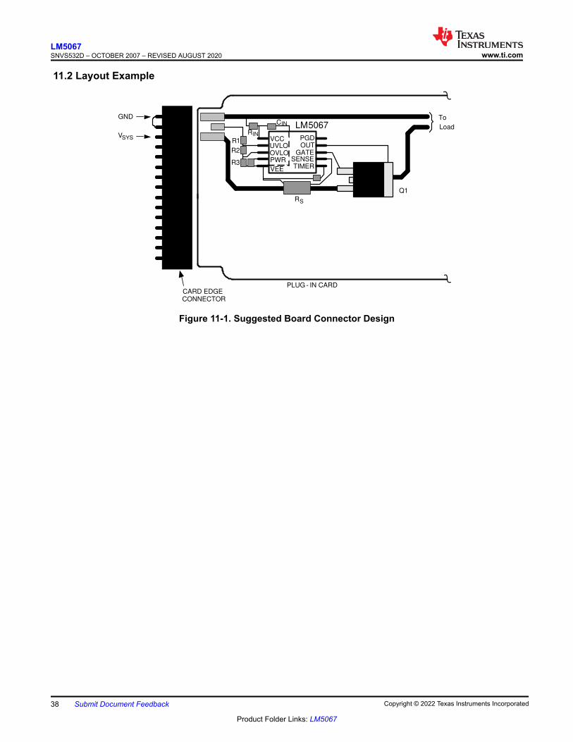
11.2 Layout Example
GND
CARD EDGE
CONNECTOR
SENSE
VCC
UVLO
OVLO
VEE
GATE
OUT
PGD
PWRTIMER
R1
R2
R3
RIN
LM5067
RS
CIN
To
Load
PLUG - IN CARD
VSYS
Q1
Figure 11-1. Suggested Board Connector Design
LM5067SNVS532D – OCTOBER 2007 – REVISED AUGUST 2020 www.ti.com
38 Submit Document Feedback Copyright © 2022 Texas Instruments Incorporated
Product Folder Links: LM5067
12 Device and Documentation Support12.1 TrademarksAll trademarks are the property of their respective owners.12.2 Electrostatic Discharge Caution
This integrated circuit can be damaged by ESD. Texas Instruments recommends that all integrated circuits be handled with appropriate precautions. Failure to observe proper handling and installation procedures can cause damage.ESD damage can range from subtle performance degradation to complete device failure. Precision integrated circuits may be more susceptible to damage because very small parametric changes could cause the device not to meet its published specifications.
12.3 GlossaryTI Glossary This glossary lists and explains terms, acronyms, and definitions.
www.ti.comLM5067
SNVS532D – OCTOBER 2007 – REVISED AUGUST 2020
Copyright © 2022 Texas Instruments Incorporated Submit Document Feedback 39
Product Folder Links: LM5067
13 Mechanical, Packaging, and Orderable InformationThe following pages include mechanical, packaging, and orderable information. This information is the most current data available for the designated devices. This data is subject to change without notice and revision of this document. For browser-based versions of this data sheet, refer to the left-hand navigation.
LM5067SNVS532D – OCTOBER 2007 – REVISED AUGUST 2020 www.ti.com
40 Submit Document Feedback Copyright © 2022 Texas Instruments Incorporated
Product Folder Links: LM5067
PACKAGE OPTION ADDENDUM
www.ti.com 10-Dec-2020
Addendum-Page 1
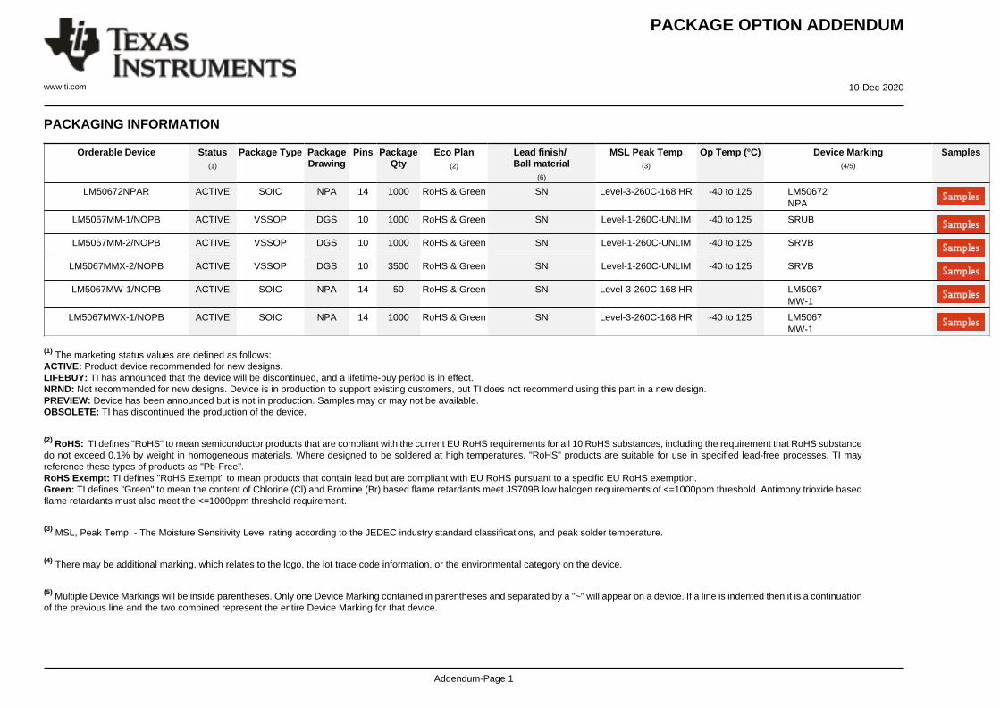
PACKAGING INFORMATION
Orderable Device Status(1)
Package Type PackageDrawing
Pins PackageQty
Eco Plan(2)
Lead finish/Ball material
(6)
MSL Peak Temp(3)
Op Temp (°C) Device Marking(4/5)
Samples
LM50672NPAR ACTIVE SOIC NPA 14 1000 RoHS & Green SN Level-3-260C-168 HR -40 to 125 LM50672NPA
LM5067MM-1/NOPB ACTIVE VSSOP DGS 10 1000 RoHS & Green SN Level-1-260C-UNLIM -40 to 125 SRUB
LM5067MM-2/NOPB ACTIVE VSSOP DGS 10 1000 RoHS & Green SN Level-1-260C-UNLIM -40 to 125 SRVB
LM5067MMX-2/NOPB ACTIVE VSSOP DGS 10 3500 RoHS & Green SN Level-1-260C-UNLIM -40 to 125 SRVB
LM5067MW-1/NOPB ACTIVE SOIC NPA 14 50 RoHS & Green SN Level-3-260C-168 HR LM5067MW-1
LM5067MWX-1/NOPB ACTIVE SOIC NPA 14 1000 RoHS & Green SN Level-3-260C-168 HR -40 to 125 LM5067MW-1
(1) The marketing status values are defined as follows:ACTIVE: Product device recommended for new designs.LIFEBUY: TI has announced that the device will be discontinued, and a lifetime-buy period is in effect.NRND: Not recommended for new designs. Device is in production to support existing customers, but TI does not recommend using this part in a new design.PREVIEW: Device has been announced but is not in production. Samples may or may not be available.OBSOLETE: TI has discontinued the production of the device.
(2) RoHS: TI defines "RoHS" to mean semiconductor products that are compliant with the current EU RoHS requirements for all 10 RoHS substances, including the requirement that RoHS substancedo not exceed 0.1% by weight in homogeneous materials. Where designed to be soldered at high temperatures, "RoHS" products are suitable for use in specified lead-free processes. TI mayreference these types of products as "Pb-Free".RoHS Exempt: TI defines "RoHS Exempt" to mean products that contain lead but are compliant with EU RoHS pursuant to a specific EU RoHS exemption.Green: TI defines "Green" to mean the content of Chlorine (Cl) and Bromine (Br) based flame retardants meet JS709B low halogen requirements of <=1000ppm threshold. Antimony trioxide basedflame retardants must also meet the <=1000ppm threshold requirement.
(3) MSL, Peak Temp. - The Moisture Sensitivity Level rating according to the JEDEC industry standard classifications, and peak solder temperature.
(4) There may be additional marking, which relates to the logo, the lot trace code information, or the environmental category on the device.
(5) Multiple Device Markings will be inside parentheses. Only one Device Marking contained in parentheses and separated by a "~" will appear on a device. If a line is indented then it is a continuationof the previous line and the two combined represent the entire Device Marking for that device.
PACKAGE OPTION ADDENDUM
www.ti.com 10-Dec-2020
Addendum-Page 2
(6) Lead finish/Ball material - Orderable Devices may have multiple material finish options. Finish options are separated by a vertical ruled line. Lead finish/Ball material values may wrap to twolines if the finish value exceeds the maximum column width.
Important Information and Disclaimer:The information provided on this page represents TI's knowledge and belief as of the date that it is provided. TI bases its knowledge and belief on informationprovided by third parties, and makes no representation or warranty as to the accuracy of such information. Efforts are underway to better integrate information from third parties. TI has taken andcontinues to take reasonable steps to provide representative and accurate information but may not have conducted destructive testing or chemical analysis on incoming materials and chemicals.TI and TI suppliers consider certain information to be proprietary, and thus CAS numbers and other limited information may not be available for release.
In no event shall TI's liability arising out of such information exceed the total purchase price of the TI part(s) at issue in this document sold by TI to Customer on an annual basis.
TAPE AND REEL INFORMATION
*All dimensions are nominal
Device PackageType
PackageDrawing
Pins SPQ ReelDiameter
(mm)
ReelWidth
W1 (mm)
A0(mm)
B0(mm)
K0(mm)
P1(mm)
W(mm)
Pin1Quadrant
LM50672NPAR SOIC NPA 14 1000 330.0 16.4 10.9 9.5 3.2 12.0 16.0 Q1
LM5067MM-1/NOPB VSSOP DGS 10 1000 178.0 12.4 5.3 3.4 1.4 8.0 12.0 Q1
LM5067MM-2/NOPB VSSOP DGS 10 1000 178.0 12.4 5.3 3.4 1.4 8.0 12.0 Q1
LM5067MMX-2/NOPB VSSOP DGS 10 3500 330.0 12.4 5.3 3.4 1.4 8.0 12.0 Q1
LM5067MWX-1/NOPB SOIC NPA 14 1000 330.0 16.4 10.9 9.5 3.2 12.0 16.0 Q1
PACKAGE MATERIALS INFORMATION
www.ti.com 9-Apr-2022
Pack Materials-Page 1
*All dimensions are nominal
Device Package Type Package Drawing Pins SPQ Length (mm) Width (mm) Height (mm)
LM50672NPAR SOIC NPA 14 1000 356.0 356.0 35.0
LM5067MM-1/NOPB VSSOP DGS 10 1000 208.0 191.0 35.0
LM5067MM-2/NOPB VSSOP DGS 10 1000 208.0 191.0 35.0
LM5067MMX-2/NOPB VSSOP DGS 10 3500 367.0 367.0 35.0
LM5067MWX-1/NOPB SOIC NPA 14 1000 356.0 356.0 35.0
PACKAGE MATERIALS INFORMATION
www.ti.com 9-Apr-2022
Pack Materials-Page 2
TUBE
*All dimensions are nominal
Device Package Name Package Type Pins SPQ L (mm) W (mm) T (µm) B (mm)
LM5067MW-1/NOPB NPA SOIC 14 50 495 15 5842 7.87
PACKAGE MATERIALS INFORMATION
www.ti.com 9-Apr-2022
Pack Materials-Page 3
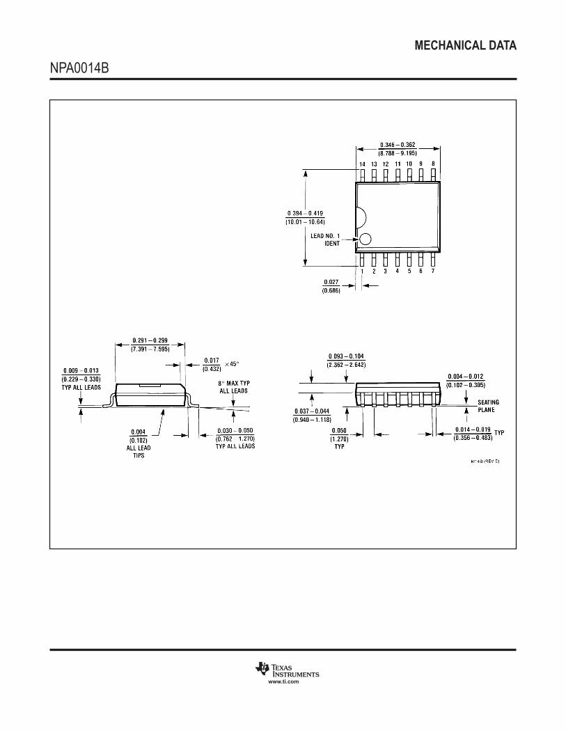
MECHANICAL DATA
NPA0014B
www.ti.com
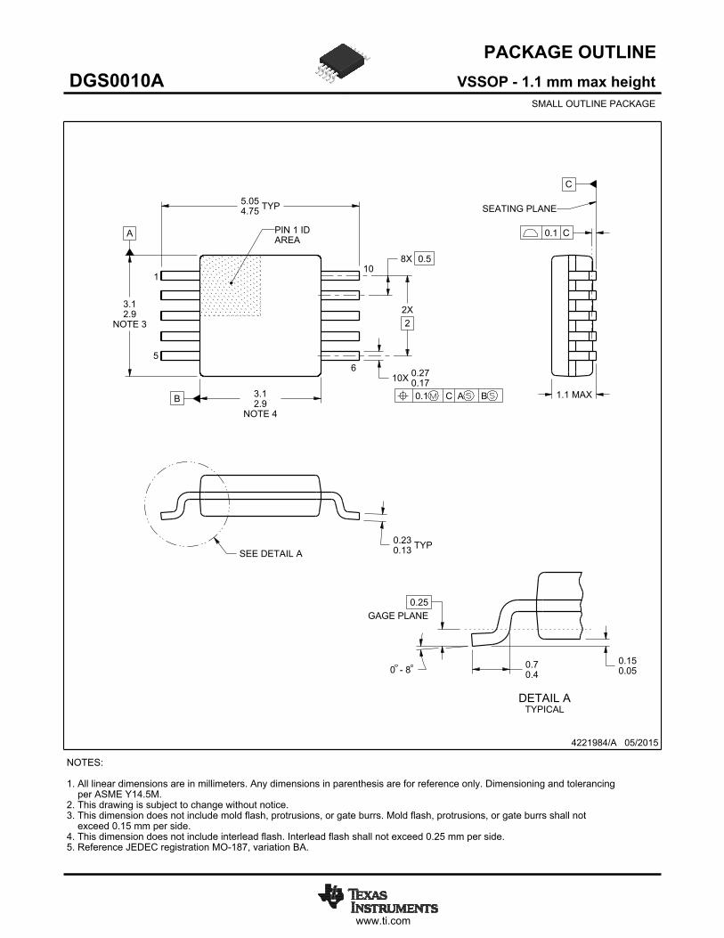
www.ti.com
PACKAGE OUTLINE
C
TYP5.054.75
1.1 MAX
8X 0.5
10X 0.270.17
2X2
0.150.05
TYP0.230.13
0 - 8
0.25GAGE PLANE
0.70.4
A
NOTE 3
3.12.9
BNOTE 4
3.12.9
4221984/A 05/2015
VSSOP - 1.1 mm max heightDGS0010ASMALL OUTLINE PACKAGE
NOTES: 1. All linear dimensions are in millimeters. Any dimensions in parenthesis are for reference only. Dimensioning and tolerancing per ASME Y14.5M. 2. This drawing is subject to change without notice. 3. This dimension does not include mold flash, protrusions, or gate burrs. Mold flash, protrusions, or gate burrs shall not exceed 0.15 mm per side. 4. This dimension does not include interlead flash. Interlead flash shall not exceed 0.25 mm per side.5. Reference JEDEC registration MO-187, variation BA.
110
0.1 C A B
65
PIN 1 IDAREA
SEATING PLANE
0.1 C
SEE DETAIL A
DETAIL ATYPICAL
SCALE 3.200
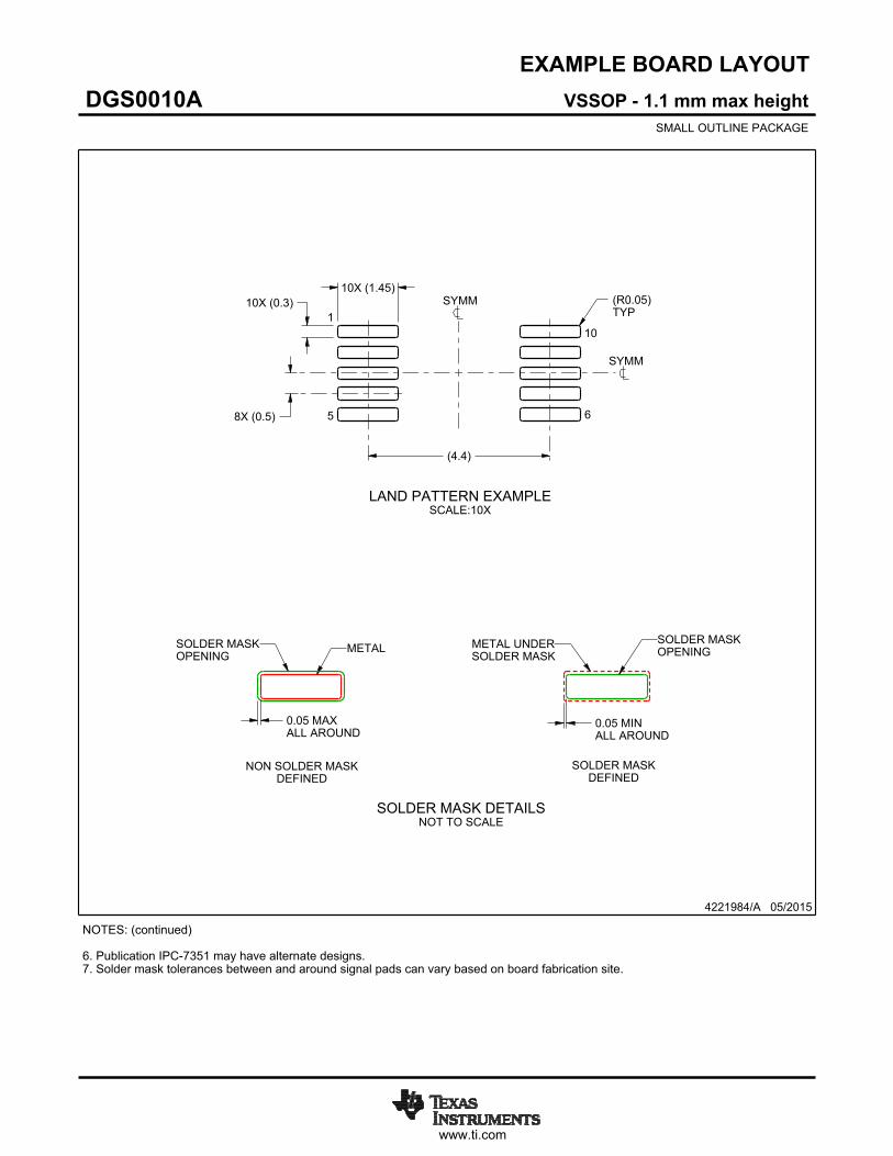
www.ti.com
EXAMPLE BOARD LAYOUT
(4.4)
0.05 MAXALL AROUND
0.05 MINALL AROUND
10X (1.45)10X (0.3)
8X (0.5)
(R )TYP
0.05
4221984/A 05/2015
VSSOP - 1.1 mm max heightDGS0010ASMALL OUTLINE PACKAGE
SYMM
SYMM
LAND PATTERN EXAMPLESCALE:10X
1
5 6
10
NOTES: (continued) 6. Publication IPC-7351 may have alternate designs. 7. Solder mask tolerances between and around signal pads can vary based on board fabrication site.
METALSOLDER MASKOPENING
NON SOLDER MASKDEFINED
SOLDER MASK DETAILSNOT TO SCALE
SOLDER MASKOPENING
METAL UNDERSOLDER MASK
SOLDER MASKDEFINED
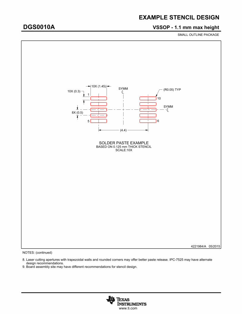
www.ti.com
EXAMPLE STENCIL DESIGN
(4.4)
8X (0.5)
10X (0.3)10X (1.45)
(R ) TYP0.05
4221984/A 05/2015
VSSOP - 1.1 mm max heightDGS0010ASMALL OUTLINE PACKAGE
NOTES: (continued) 8. Laser cutting apertures with trapezoidal walls and rounded corners may offer better paste release. IPC-7525 may have alternate design recommendations. 9. Board assembly site may have different recommendations for stencil design.
SYMM
SYMM
1
5 6
10
SOLDER PASTE EXAMPLEBASED ON 0.125 mm THICK STENCIL
SCALE:10X
IMPORTANT NOTICE AND DISCLAIMERTI PROVIDES TECHNICAL AND RELIABILITY DATA (INCLUDING DATA SHEETS), DESIGN RESOURCES (INCLUDING REFERENCE DESIGNS), APPLICATION OR OTHER DESIGN ADVICE, WEB TOOLS, SAFETY INFORMATION, AND OTHER RESOURCES “AS IS” AND WITH ALL FAULTS, AND DISCLAIMS ALL WARRANTIES, EXPRESS AND IMPLIED, INCLUDING WITHOUT LIMITATION ANY IMPLIED WARRANTIES OF MERCHANTABILITY, FITNESS FOR A PARTICULAR PURPOSE OR NON-INFRINGEMENT OF THIRD PARTY INTELLECTUAL PROPERTY RIGHTS.These resources are intended for skilled developers designing with TI products. You are solely responsible for (1) selecting the appropriate TI products for your application, (2) designing, validating and testing your application, and (3) ensuring your application meets applicable standards, and any other safety, security, regulatory or other requirements.These resources are subject to change without notice. TI grants you permission to use these resources only for development of an application that uses the TI products described in the resource. Other reproduction and display of these resources is prohibited. No license is granted to any other TI intellectual property right or to any third party intellectual property right. TI disclaims responsibility for, and you will fully indemnify TI and its representatives against, any claims, damages, costs, losses, and liabilities arising out of your use of these resources.TI’s products are provided subject to TI’s Terms of Sale or other applicable terms available either on ti.com or provided in conjunction with such TI products. TI’s provision of these resources does not expand or otherwise alter TI’s applicable warranties or warranty disclaimers for TI products.TI objects to and rejects any additional or different terms you may have proposed. IMPORTANT NOTICE
Mailing Address: Texas Instruments, Post Office Box 655303, Dallas, Texas 75265Copyright © 2022, Texas Instruments Incorporated