LE VIET DUC Computing the Relative Permittivity and Loss ...
66
LE VIET DUC Computing the Relative Permittivity and Loss Tangent of Substrates by the Numerical Model of a Microstrip Transmission Line Master of Science Thesis Examiner: Academy Research Fel- low, Toni Björninen and Academy Research Fellow Johanna Virkki Examiner and topic approved on 25 May 2018
-
Upload
khangminh22 -
Category
Documents
-
view
2 -
download
0
Transcript of LE VIET DUC Computing the Relative Permittivity and Loss ...
LE VIET DUC Computing the Relative Permittivity and Loss Tangent of Substrates by the Numerical Model of a Microstrip Transmission Line Master of Science Thesis
Examiner: Academy Research Fel-low, Toni Björninen and Academy Research Fellow Johanna Virkki Examiner and topic approved on 25 May 2018

1
ABSTRACT DUC LE: Method for Measuring the Relative Permittivity and Loss Tangent of EPDM cell rubber foam Substrates by Inversion of the Numerical Model of a Microstrip Trans-mission Line and Application to Optimising Wearable EPDM cell rubber foam Antennas. Tampere University of Technology Master of Science Thesis, 50 pages, 5 Appendix pages May 2018 Master’s Degree Programme in Electrical Engineering Major: Electronics Examiner: Academy Research Fellow Toni Björninen and Academy Research Fellow Johanna Virkki Keywords: RF,model, transmission lines, practical transmission line measure-ments The microstrip transmission line numerical model is used to search out the rela-tive permittivity and loss tangent of the materials of the substrate at the high fre-quency range (400 MHz – 3GHz). This thesis shows outcomes of the transmis-sion line numerical model in simulation software ADS and those of practical im-plement. The microstrip transmission line was measured by vector network ana-lyzer. There are multiple substrate materials employed namely, FR4, AR1000, EPDM cell rubber foam, wood, wood wet. The substrate material FR4 and AR1000 play as reference material to examine the efficiency of the numerical model. The wood wet was used to check the increase of the relative permittivity and loss tangent when the moisture in the substrate levels up. Additionally, the surface roughness measurement data is also added in the model in order to make model as similar to real device under test as possible. The dimenision and size of the microstrip lines in model are identical to the practical line to reduce the mismatch of the outcomes. The choosing results of the relative permittivity and loss tangent based on the maximum attainable power gain comparision between the model and practical measurement results. The best data is selected based on the least squares method estimation. In order to assess the accuracy of the found relative permit-tivity and loss tangent, the low pass filter and passive UHF RFID antenna are employed. The comparision between the model and measurement results of these devices are used. In this thesis, fundamental knowledge related to microstrip transmission lines and the least squares method will be taken into account. Finally, the future works to improve the transmission line model will be discussed in the conclusion part.

2 PREFACE This thesis was done at Tampere University of Technology, Finland. I feel quite glad since I am able to finish it finally. I am grateful to my supervisors and examiners, Toni Björninen and Johanna Virkki for providing me the interesting thesis topic for my Master degree. I also say thank to all of their supervision and advice that I granted during either lab work or thesis writing.I also would like to thank RF group for their assistance and their advice. I am indebted also to many colleagues for their support and contributions. Finally, I would like to extend my gratitude to the whole RFID group for the invariably enthusiastic and pleasant work atmosphere. During doing thesis, I had a chance to make friends and discuss with other friends in the wireless communication group. My final thanks belong to Giau Huynh for loving and believing in me , my friends and my family members for providing support throughout this thesis work. Tampere, 21.5.2018 Le Viet Duc
3 CONTENTS 1. INTRODUCTION ................................................................................................ 9
2. THEORY BACKGROUND ................................................................................ 11
2.1 Transmission line theory ........................................................................... 11
2.2 Microstrip line theory ............................................................................... 14
2.3 Loss tangent and permittivity .................................................................... 17
2.4 Scattering Parameters ............................................................................... 18
3. OVERVIEW OF NUMERICAL METHODS ...................................................... 19
3.1 The least square estimation method ........................................................... 19
3.2 Modeling conducting method .................................................................... 20
3.3 The numerical modeling method ............................................................... 22
4. THE TEST SAMPLE STRUCTRURE ................................................................ 23
4.1 The microstrip lines .................................................................................. 23
4.2 Low pass filter .......................................................................................... 24
4.3 Passive RFID antennas ............................................................................. 25
4.3.1 Operation principle of Passive Long range UHF RFID System ... 26
5. MEASUREMENT SETUP.................................................................................. 28
5.1 The microstrip transmission line and low pass filter measurement setup ... 28
5.2 The passive UHF RFID antenna measurement .......................................... 29
5.3 The surface roughness measurement ......................................................... 31
6. THE SIMULATION MODEL............................................................................. 33
6.1 Choosing the solver .................................................................................. 33
6.2 The simulation model structures ............................................................... 33
6.2.1 Transmission line model ............................................................. 34
6.2.2 The low pass filter model ............................................................ 36
6.2.3 RFID tag antenna model ............................................................. 37
7. MEASUREMENT RESULTS ............................................................................. 38
7.1 Surface roughness measurement ............................................................... 39
7.2 Microstrip lines results analyzing .............................................................. 41
7.2.1 FR4 microstrip line ..................................................................... 41
7.2.2 AR 1000 microstrip line .............................................................. 43
7.2.3 EPDM cell rubber foam microstrip line ....................................... 45
7.2.4 Wood microstrip line .................................................................. 47
7.2.5 Wood wet microstrip line ............................................................ 50
7.3 Comparing the results of modeling and measurement of low pass filter (FR4) 53
7.4 Comparing the read range of modeling and measurement of UHF RFID antenna (EPDM cell rubber foam). ..................................................................... 55
CONCLUSIONS ........................................................................................................ 56
8. REFERENCES ................................................................................................... 57

4 APPENDIX A: Matlab code

5 LIST OF FIGURES
The lumped equivalent circuit of the transmission line ......................... 12
The transmission line connects to the load ............................................ 13
The geometry of the microstrip line [28] .............................................. 14
The transmission line model with incident and reflected waves ............. 15
The S scattering ................................................................................... 18
The structures of the transmission lines ................................................ 23
The wood microstrip transmission line in a bow of water ..................... 24
The low pass stub filter ......................................................................... 24
The EPDM cell rubber foam RFID tag ................................................. 25
The geometry of the RFID tag [11] ...................................................... 26
The main components and operation principle of the passive RFID system [12] .......................................................................................... 26
The microstrip transmission line measurement ..................................... 28
The low pass stub filter measurement ................................................... 29
The antenna measuring system [31] ..................................................... 29
The UHF RFID antenna measurement ................................................. 30
The roughness measurement of the microstrip line ............................... 31
The surface roughness measurement principle ..................................... 32
The microstrip line model ..................................................................... 34
The maximum attainable power gain versus frequency ......................... 35
The swept S11 and S21 of the transmission line simulation model ........ 35
The schematic of low pass stub filter simulation model ......................... 36
The layout of the low pass filter ............................................................ 36
The UHF RFID antenna structure ........................................................ 37
Roughness measuring data of FR4 ....................................................... 39
The S parameters comparison between simulation model and measurement results ............................................................................. 41
The maximum attainable power gain comparison between simulation model and the practical measurement result........................ 42
The permittivity and loss tangent versus frequency ............................... 42
The S parameters comparison between simulation model and measurement results of AR1000 substrate ............................................ 43
The comparison between the measured and simulation maximum attainable power gain versus frequency ................................................ 44
The permittivity and loss tangent versus frequency of AR1000 substrate model .................................................................................... 44
The comparison of S parameters between measurement and model of EPDM cell rubber foam microstrip line ............................................ 46
6 The comparison between the measurement and model maximum
attainable power gain of the EPDM cell rubber foam transmission line ....................................................................................................... 46
The permittivity and loss tangent of the EPDM cell rubber foam substrate model .................................................................................... 47
The S parameters comparison between the measurement and model of wood microstrip line......................................................................... 48
The permittivity and loss tangent of the wood substrate model .............. 49
The maximum attainable power gain result comparison between measurement and model versus frequency ............................................ 49
The S parameters comparison between the measurement and model of the wood wet microstrip line ............................................................. 50
The maximum attainable power gain result comparison between measurement and model versus frequency of the wood wet transmission line .................................................................................. 51
The relative permittivity and loss tangent of the wood wet substrate model ................................................................................................... 51
The transducer gain comparison between the model and practical low pass stub filter ............................................................................... 53
The reflection coefficient comparison of the practical (blue line) and model (red line) low pass stub filter ............................................... 54
The read range of model and practical antenna versus frequency ......... 55
Initialize and import measured data ..................................................... 61
The least squares estimation algorithm................................................. 62
The calculation of the relative permittivity and loss tangent ................. 63
Presenting the results ........................................................................... 63
Comparing the model results with the practical measurement .............. 64
The PCB layout of the microtrip transmission lines .............................. 65

7 LIST OF SYMBOLS AND ABBREVIATIONS 𝑡𝑎𝑛𝛿𝑒𝑓𝑓 Effective loss tangent or dissipation factor 휀𝑟𝑒𝑓𝑓 Effective relative permittivity ADS Advanced Design System RF Radio Frequency UHF Ultra High Frequency RFID Radio Frequency Identification VNA Vector network analyzer TEM Transverse electromagnetic R Resistance of finite conductivity L Self-inductance of two conductors VSI Vertical scanning interferometry DUT Device under test v(z,t) Voltage across a segment z i(z,t) Voltage across a segment z C Shunt capacitance per unit length are per-unit-length quantities G Shunt conductance per unit length or dielectric loss in the material between the conductors γ Propagation constant α Attenuation constant β Phase constant j Complex munber ω Angular frequency V+ Incident voltage V- Reflected voltage I+ Incident current I- Incident currrent ZL Load impedance Z0 Characteristic impedance Zin Input impedance Γ Reflection coefficient 𝑣𝑝 Phase velocity c Speed of light λ Wave length f Frequency λ0 Wave length of light μr Complex permeability S11 Port 1 reflection coefficient S12 Port 1 gain or attenuation S21 Port 2 gain or attenuation S22 Port 2 reflection coefficient ε' Real part of relative permittivity ε" Imaginary part of relative permittivity 𝜎𝑒 Effective conductivity 𝜎𝑠 Static conductivity H Magnetizing field J Current density E Electric field

8 D Displacement field Zs Surface impedance W Width L Length a Gap length b Gap width c IC gap length dB Decibel number GHz Gigahertz MHz Megahertz 𝛿 Skin depth
9 1. INTRODUCTION Nowadays, instead of using conventional materials for antenna or RF circuits design, new materials as wood, fabric, plastic, paper and EPDM cell rubber foam that are low cost, eco-friendly and easily available. However, exploring the characterization such as the permittivity and loss tangent for these new substrate materials for the high frequency are a challenge. Some previous research for the characterization of the substrate can be found in [20] [29], application note [21], and the book [22]. The two-line method was introduced in [38], however, it is not able to directly calculate the loss tangent. The conventional methods have to use complicated procedures or extremely immoderate cost for the meas-urement devices to find the characterization of new substrate materials. To solve above-mentioned challenges, the ultimate goal of this thesis is to single out the relative permit-tivity and the loss tangent by the numerical transmission line model. The main strategy is based on the comparison between outcomes of the simulation model and practical meas-urement results. This method holds the promise to be low cost, speedy, uncomplicated and easily applicable. While, the accuracy of this method is acceptable and meets require-ments of conscientious tests. The numerical microstrip transmission line model will be constructed with some crucial procedures. First of all, the practical transmission lines will be conducted and measured to achieve the S parameters and the maximum attainable power gain will be computed. The size and the dimension of the practical transmission line are inserted to those of nu-merical model in the simulation software (ADS- Advanced Design System) to make sure that there is no mismatch between the model and practical transmission lines. On the other hands, the conducting surface roughness is measured by profiliometer and inserted to the model. By this way, the impacts of roughness to the S parameters and the attenuation of the microstrip line will be taken into consideration. By sweeping the maximum attainable power gain in ADS and comparing those with practical measurement by the least squares estimation method, the relative permittivity and loss tangent can be found. After that, the found relative permittivity and loss tangent will be rigorously inspected by several meth-ods. The ubiquitous materials (FR4, AR1000) will be compared with data from manufac-turers. If the results are satisfied, other results of less common materials such as wood, EPDM cell rubber foam will be acceptable. Additionally, to check the accuracy of the model method, the low pass stub filter and passive UHF RFID antenna are used. The thesis is organized as follows. Chapter 2 introduces the reader to fundamentals theory background of the microstrip lines, the relative permittivity, loss tangent and the S scat-tering parameters. Chapters 3 tells readers the overview of the numerical model where the least squares estimation and the numerical method in this thesis are briefly introduced. Chapter 4 focuses on the practical test sample structures namely, transmission lines, low

10 pass stub filter and the passive UHF RFID antennas. Chapter 5 demonstrates the meas-urement setup of the testing structures. Chapter 6 depicts the numerical simulation model of the transmission line, low pass filter and the RFID antenna. The analyzing measure-ment results are illustrated in Chapter 7. Followed by the conclusion in Chapter 8.

11 2. THEORY BACKGROUND In this Chapter, some theoretical aspects namely, transmission line, microstrip line, loss tangent ( 𝑡𝑎𝑛𝛿𝑒𝑓𝑓), relative permittivity (휀𝑟𝑒𝑓𝑓) and S parameters are introduced. The transmission line theory focuses on the mathematic equations demonstrating the propa-gation of electromagnetic wave inside transmission line. Besides, the theories of reflec-tion coefficient and the impedance of transmission line are established. The next part is the microstrip line theory. This part shows the geometry of the microstrip line, propaga-tion constant and relation of the relection coefficient and the S scattering paramters. The third part is the introduction of the relative permittivity and the loss tangent. Finally, one of the crucial part in this section is the theory of the S scattering parametrers. This part shows definition of S parameters which is based on the incident and reflection waves. 2.1 Transmission line theory The transmission line is played as a conductor where the wavelength is comparable to the size of the line. At high frequency, the voltage and current are not constant through the length of the transmission line due to the propagation delay comparable to the signal pe-riod [1]. On the other hands, the current and voltage across the transmission line are as-sumed as constant when the frequency is low enough. A two-wire line is able to schematically illustrate the transmission line because all con-ducting lines include at least two conductors, for example, the ground plane and conduct-ing plane in term of the transverse electromagnetic [TEM] wave propagation. On the other hands, the lumped-component circuit is capable of modeling the infinitesimal piece ∆𝑧 of the transmission line. The equivalent lump components circuit possesses certain proper-ties as follows: R=resistance of finite conductivity, L=self-inductance of two conductors, G = shunt conductance per unit length or dielectric loss in the material between the con-ductors , and C=shunt capacitance per unit length are per-unit-length quantities, 𝑖(𝑧, 𝑡) and 𝑣(𝑧, 𝑡) respectively stands for the current and voltage at one specific point on the line at a certain time [1].

12
The lumped equivalent circuit of the transmission line Employing the Ohms and voltage Kirchhoff’s law for circuit in Figure 1, the following equation can be expressed [1]:
𝑣(𝑧, 𝑡) = 𝑅∆𝑧 𝑖(𝑧, 𝑡) + 𝐿∆𝑧𝜕𝑖(𝑧,𝑡)
𝜕𝑡+ 𝑣(𝑧 + ∆𝑧, 𝑡) (2.1)
Since we are analyzing the infinitesimal segment of a transmission line, hence, ∆𝑧 is ap-proximately 0. Therefore, the equation (2.1) is rearrange as division with ∆𝑧 and deriva-tive [1]:
𝜕𝑣(𝑧,𝑡)
𝜕𝑧= −𝑅𝑖(𝑧, 𝑡) − 𝐿
𝜕𝑖(𝑧,𝑡)
𝜕𝑡 (2.2)
Next, Kirchhoff’s current law can also be applied for the circuit presented in Figure 1[1]: 𝑖(𝑧, 𝑡) = 𝐶∆𝑧
𝑣(𝑧+∆𝑧,𝑡)
𝜕𝑡+ 𝐺∆𝑧 𝑣(𝑧 + ∆𝑧, 𝑡) + 𝑢(𝑧 + ∆𝑧, 𝑡) (2.3)
Again, when ∆𝑧 proceed toward to 0, the equation (2.3) can be expressed: 𝜕𝑖(𝑧,𝑡)
𝜕𝑧= −𝐺 𝑣(𝑧, 𝑡) − 𝐶
𝜕𝑣(𝑧,𝑡)
𝜕𝑡 (2.4)
For the sinusoidal steady-state condition, with cosine-based phasors, (2.2) and (2.4) trans-form to:
𝑑𝑉(𝑧)
𝜕𝑧= −(𝑅 + 𝑗𝜔𝐿)𝐼(𝑧) (2.5)
𝑑𝐼(𝑧)
𝜕𝑧= −(𝐺 + 𝑗𝜔𝐶)𝑉(𝑧) (2.6)
These equation (2.5) and (2.6) are 𝑑2𝑉(𝑧)
𝑑𝑧2 − 𝛾2𝑉(𝑧) = 0 (2.7) 𝑑2𝐼(𝑧)
𝑑𝑧2 − 𝛾2𝐼(𝑧) = 0 (2.8) where
13 𝛾 = 𝛼 + 𝑗𝛽 = √(𝑅 + 𝑗𝜔𝐿)(𝐺 + 𝑗𝜔𝐶) (2.9)
is the propagation constant as a function of frequency. The travelling wave equation form of (2.7) and (2.8) can be found as [1]:
𝑉(𝑧) = 𝑉+𝑒−𝛾𝑧+𝑉−𝑒𝛾𝑧 (2.10) 𝐼(𝑧) = 𝐼+𝑒−𝛾𝑧- 𝐼−𝑒𝛾𝑧 (2.11)
where the 𝑒−𝛾𝑧 and 𝑒𝛾𝑧 depicts the wane propagation in the +𝑧 (forward) and –z (re-flected) direction. The characteristic impedance 𝑍0 can be found based on the voltage and current on the line as follows: 𝑉0
+
𝐼0+ = 𝑍0 =
−𝑉0−
𝐼0− (2.12)
The equation (2.10) and (2.11) can be reorganized based on wave propagation in the fol-lowing form [1]:
𝐼(𝑧) =𝑉0
+
𝑍0𝑒−𝛾𝑧 −
𝑉0−
𝑍0𝑒𝛾𝑧 (2.13)
From the equation (13), it is can be comprehended that the total current of a transmission line contains the incident and the reflected waves. The reflection coefficient (Γ)is a unit showing the relationship between waves leaving the load (𝑉−)𝑒𝛾𝑧|𝑍=0 = 𝑉− and incident waves to the load (𝑉+)𝑒−𝛾𝑧|𝑍=0 = 𝑉+ . It is based on the characteristic impedance 𝑍0 and the load impedance 𝑍𝐿. The equation of reflection coefficient is represented as:
Γ=𝑉−
𝑉+ =𝑍𝐿−𝑍0
𝑍𝐿+𝑍0 (2.14)
When we align a coordinate axis to the transmission line where the load is at zero point Z=0 [1].
The transmission line connects to the load

14 The transmission line input impedance at distance L connected to the load can be defined basing on the relation between the incident and reflected waves [1].
𝑍𝑖𝑛 =𝑉(−𝐿)
𝐼(−𝐿)=
𝑉+𝑒𝛾𝑧+𝑉−𝑒−𝛾𝑧
𝑉+𝑒𝛾𝑧−𝑉−𝑒−𝛾𝑧 𝑍0 (2.15) The input impedance of a transmission line can be formed by the characteristic impedance and the load impedance when combine equation (2.14) and (2.15) [35]:
𝑍𝑖𝑛 = 𝑍0𝑍𝐿+𝑗𝑍0𝑡𝑎𝑛𝛽𝑙
𝑍0+𝑗𝑍𝐿𝑡𝑎𝑛𝛽𝑙 (2.16)
2.2 Microstrip line theory The microstrip line is a shape of the electrical transmission line which is a combination of the strip conductor and a ground plane separated by dielectric layer or substrate [27]. The conductor and ground plane are commonly made by copper possessing conductivity 5.8x10⁷ (
𝑆
𝑚) and some typical types of the dielectric substrates are FR4, RT/Duroid, Rog-
ers Corporation, Chandler, Arizona, which obtain the available permittivity 𝜖𝑟 such as FR4 𝜖𝑟 ≅ 4.2 … 4.6, AD1000 𝜖𝑟 ≅ 10.2 … 13, RO4000 𝜖𝑟 ≅ 3.66. The electromagnetic wave transformed by microstrip line not entirely remains in the sub-strate and partly in the air above the line [37].
The geometry of the microstrip line [28] Figure 3 illustrates the quasi/TEM behavior of a microstrip line. Assuming a quasi/TEM mode of propagation in the microstrip line, the phase velocity can be found:
𝑣𝑝 =𝑐
√ 𝑒𝑓𝑓 (2.17)
where: c is the speed of light (3x10⁸ 𝑚/𝑠) and 휀𝑒𝑓𝑓 is the relative dielectric constant of the microstrip. Another form of phase velocity equation related to the inductance per unit length (L) and the capacitance per unit length (C).
15 𝑣𝑝 =
1
√𝐿𝐶 (2.18)
The wavelength in the microstrip line is given by: 𝜆 =
𝑐
𝑓√ 𝑒𝑓𝑓=
𝑣𝑝
𝑓 =
𝜆0
√ 𝑒𝑓𝑓 (2.19)
where 𝜆0 is the free space wavelength [1]. The propagation constant 𝛽 is defined by [1]:
𝛽 = 𝑘0. √휀𝑒𝑓𝑓 (2.20) The microstrip line is characterized by its attenuation due to the conductor and dielectric losses when electromagnetic wave propagates along the microstrip line. In this thesis, we will study the calculation of the permittivity and the loss tangent. The transmission line methods employing a segment of the transmission line as a sample under test. From the scattering parameters, the electromagnetic properties of the material under test, its permittivity and permeability, can be extracted. In such a method all the four scattering parameters can be measured. A segment of a rectangular waveguide is played as a sample of peace of transmission line filling the line and leaving no air gaps is a typical measurement configuration. The model is placed along x-direction same with the wave propagation direction [2].
The transmission line model with incident and reflected waves As shown in figure 4, E𝐼 , E𝐼𝐼 , E𝐼𝐼𝐼 are three sections of electric filed of the segment. For a normalized incident wave is
𝐸𝐼 = 𝑒(−𝛾𝑜𝑥) + 𝐶1𝑒(𝛾𝑜𝑥) (2.21) 𝐸𝐼𝐼 = 𝐶2𝑒(−𝛾𝑜𝑥) + 𝐶3𝑒(𝛾𝑜𝑥) (2.22)
𝐸𝐼 = 𝐶4𝑒(−𝛾𝑜𝑥) (2.23) with

16
𝛾𝑜 = 𝑗√(𝜔
𝑐)
2
− (2𝜋
𝜆𝑐)
2 (2.24)
𝛾 = 𝑗√(𝜔𝜇𝑟 𝑟
𝑐)
2
− (2𝜋
𝜆𝑐)
2 (2.25) where 𝜇𝑟 is the complex permeability, 휀𝑟 is the complex permittivity, 𝑐 is the speed of light in vacuum (m/s), 𝜔 is the angular frequency and 𝜆𝑐 is the cutoff wavelength, with where a is the width of the waveguide [2]. The total length of the transmission line can be expressed:
𝐿𝑡𝑜𝑡𝑎𝑙 = 𝐿1 + 𝐿 + 𝐿2 (2.26) Where L is the length, 𝐿1 and 𝐿2 are the distance from the sample to the ports. The scattering parameters of two ports can be achieved [3]:
𝑆11 = 𝑅12 Γ(1−T2)
1−Γ2T2 (2.27) 𝑆22 = 𝑅2
2 Γ(1−T2)
1−Γ2T2 (2.28) 𝑆21 = 𝑅1𝑅2
Γ(1−T2)
1−Γ2T2 (2.29) where𝑅1 and 𝑅2 are the reference plane transformations at two ports:
𝑅𝑖 = 𝑒(−𝛾0𝐿𝑖) (𝑖 = 1,2) (2.30) The reflection coefficient [3]:
Γ =(𝛾0/𝜇0)−(𝛾/𝜇)
(𝛾0/𝜇0)+(𝛾/𝜇) (2.31)
The transmission coefficient: T = 𝑒(−𝛾𝐿) (2.32)
17 2.3 Loss tangent and permittivity The permittivity illustrates the interaction of the material with the electrical field applied into it. One effective method for demonstrating the dielectric loss is to consider the per-mittivity 휀 as a complex number defined as [4] :
휀 = 휀′ − 𝑗휀" (2.33) where 휀′ and 휀" are the real and imaginary parts of the permittivity respectively. In microwave electronics, the dimensionless quantities relative permittivity (휀𝑟) are often employed [4].
휀𝑟 =0
=′−𝑗 "
0= 휀𝑟
′ − 𝑗휀𝑟" (2.34)
where 휀0=8.854.1012 𝐹𝑚
is the free space permittivity, 휀𝑟′ is the relative dielectric constant,
휀𝑟′′ is the loss factor [4].
Maxwell’s equation for a magnetic field can be written as [5]. ∇ × �̅� = 𝐽𝑖 + 𝜎𝑠�̅� + 𝑗ω�̅� (2.35) ∇ × �̅� = 𝐽𝑖 + 𝜎𝑠�̅� + 𝑗ω(휀′ − 𝑗휀")�̅� (2.36) ∇ × �̅� = 𝐽𝑖 + (𝜎𝑠 + 𝜔휀")�̅� + 𝑗ω휀′�̅� (2.37)
if 𝜎𝑒 = 𝜎𝑠 + 𝜔휀" where 𝜎𝑒 is the effective conductivity, 𝜎𝑠 is the static conductivity, 𝜔휀"is the conductivity due to an alternating field. As the results, the loss tangent is derived from Maxwell’s equation as [5]:
∇ × �̅� = 𝐽�̅� + 𝑗ω휀′ [1 − 𝑗𝜎𝑒
ω ′] �̅� (2.38)
∇ × �̅� = 𝐽�̅� + 𝑗ω휀′[1 − 𝑗 tan 𝛿]�̅� (2.39) from equation (2.39) the dielectric loss tangent depending on frequency can be defined as [5]:
tan 𝛿𝑒 =𝜔 "+𝜎𝑒
ω ′ (2.40)

18 2.4 Scattering Parameters The RF devices (antennas, transmission lines or active circuits)or networks,in general, are characterized by S parameter from VNA ( vector network analyzer) in order to express the input and output relationship between ports. For example, S11 represents the reflec-tion at the port 1 and S21 shows the transferred power from port 2 to port 1. Therefore, an N/port network can be illustrated with N2 set of S-parameters [6].
The S scattering The S parameters can be defined by the relationship of the incident waves V+ and the reflected waves V-. The following matrix is introduced in case of an N –ports network as Figure 5 [6].
(2.40)
The simple form of the matrix is [𝑉−] = [S][𝑉+]
𝑆𝑖𝑗 =𝑉𝑖
−
𝑉𝑗+|
𝑉𝑖+≠0
(2.41) The equation (2.41) shows that the S matrix is determined by only input from port j and port I as the output port. For instance, 𝑆21 shows the insertion loss or the gain of the input port 1 and output port 2 of the 2-ports device. As another example, 𝑆11demonstrates how much the power reflected back to port 1 employed as an input. Hence, the 𝑆11 is com-monly used for studying the impedance matching or reflection coefficient of a network [6].

19 3. OVERVIEW OF NUMERICAL METHODS In this Chapter, the overview of some applied methods in this thesis such as least squares estimation, the conducting model, and the numerical model method implement. Firstly, some equations which explain the method of finding the best fitting data between the estimation and the actual measurement results. Secondly, the impedance of the conduct-ing plane is demonstrated in section 3.2. From the wave propagation, the current density in a segment of the transmission line and the characteristic impedance of the transmission line, we can found the surface impedance and apply it to the transmission line model. Last but not least, the process of building up and applying the numerical transmission line model is described in the last part of this section. Especially, the crucial steps of con-structing the transmission line model in the simulation software and testing the accuracy of the model outcomes (the relative permittivity and loss tangent) are cautiously de-scribed. The testing procedures are conducting by comparing the model results to the datasheet data from producers, practical measurements results of the low pass filter and the UHF RFID antennas. 3.1 The least square estimation method The least square method estimates the proper parameters between the measured data and the estimated values or simulation values by minimizing the squared discrepancies of them. The method is studied basing on the context of a regression, where the variation (Y) cor-responding to one variable (X). it is assumed that Y is a function of X plus the noise b [7].
𝑌 = 𝑓(𝑋) + 𝑏 (3.1) where f is a regression function which is estimated from 𝑛 coverable and their responses (𝑥1, 𝑦1), . . . , (𝑥𝑛, 𝑦𝑛). The parameter β by its square �̂� providing the best fit to the data of the measurement and the simulation. There are many possible methods to choose the parameter a and b, however the least square supports selecting a and b functionally by reducing the sum of the squared errors [7]. The least square estimator minimizes
𝐸(𝑎, 𝑏) = ∑ (𝑦𝑛 − ( 𝑎𝑥𝑛 + 𝑏))2𝑁
𝑛=1 (3.2) In term of the multivariable calculus, the value of a and b can be found by:
20 𝜕𝐸
𝜕𝑎= 0,
𝜕𝐸
𝜕𝑏= 0 (3.3)
Differentiating E (a, b) yields 𝜕𝐸
𝜕𝑎= ∑ 2(𝑦𝑛 − ( 𝑎𝑥𝑛 + 𝑏)). (−𝑥𝑛)𝑁
𝑛=1 (3.4) 𝜕𝐸
𝜕𝑏= ∑ 2(𝑦𝑛 − ( 𝑎𝑥𝑛 + 𝑏))𝑁
𝑛=1 (3.5)
setting 𝜕𝐸
𝜕𝑎=
𝜕𝐸
𝜕𝑏= 0 the (3.4) and (3.5) transformed to be [7]:
∑ 2(𝑦𝑛 − ( 𝑎𝑥𝑛 + 𝑏)). (𝑥𝑛)𝑁𝑛=1 =0 (3.6)
∑ 2(𝑦𝑛 − ( 𝑎𝑥𝑛 + 𝑏))𝑁𝑛=1 =0 (3.7)
These equations are transformed as: (∑ 𝑥𝑛
2𝑁𝑛=1 )𝑎 + (∑ 𝑥𝑛
2𝑁𝑛=1 )𝑏 = ∑ 𝑥𝑛𝑦𝑛
𝑁𝑛=1 (3.8)
(∑ 𝑥𝑛𝑁𝑛=1 )𝑎 + (∑ 1𝑁
𝑛=1 )𝑏 = ∑ 𝑦𝑛𝑁𝑛=1 (3.9)
in order to minimize the error, the value of a and b should be satisfy the matrix: (
∑ 𝑥𝑛2𝑁
𝑛=1 ∑ 𝑥𝑛𝑁𝑛=1
∑ 𝑥𝑛𝑁𝑛=1 1
) (𝑎𝑏
) = (∑ 𝑥𝑛𝑦𝑛
𝑁𝑛=1
∑ 𝑦𝑛𝑁𝑛=1
) (3.10) The matrix is invertible [7]:
(𝑎𝑏
) = (∑ 𝑥𝑛
2𝑁𝑛=1 ∑ 𝑥𝑛
𝑁𝑛=1
∑ 𝑥𝑛𝑁𝑛=1 1
)
−1
(∑ 𝑥𝑛𝑦𝑛
𝑁𝑛=1
∑ 𝑦𝑛𝑁𝑛=1
) (3.11)
3.2 Modeling conducting method At the high frequency, the current inside the transmission line (microstrip line, coplanar line) decreases exponentially with penetration into the conductor, declining to 1/e of its surface value at one skin depth [36].
𝛿 = √2
𝜔𝜇𝜎 (3.12)

21 where 𝛿 is the skin depth, 𝜇 is conductor magnetic permeability, 𝜎 is bulk conductivity, and 𝜔 is radian frequency. In the infinitely thick conductor the current density of a plane wave can be express fol-lowing the equation [8]:
𝐽(𝓏) = 𝐽0𝑒−𝓏/𝛿(cos(𝓏/𝛿) − 𝑗 sin(𝓏/𝛿)) (3.13) where 𝐽0 is the current density at surface of conductor, perpendicular to the 𝓏 axis. The thin an infinitely thin conductor with an equivalent surface impedance 𝑍𝑠 equal to the characteristic impedance 𝑍𝑂𝑀 of a plane wave propagating along the 𝓏 axis into the conductor can be employed to model a thick conductor. 𝑍𝑠 = 𝑍𝑂𝑀 = √
𝑗𝜔𝜇
𝜎= (1 + 𝑗)√
𝜔𝜇
2𝜎 (3.14)
On the other hands, the surface impedance can be found by [8]: 𝑍𝑠 = −𝑗𝑍𝑂 cot 𝑘𝑡 (3.15)
where 𝑘 = √−𝑗𝜔𝜇𝜎 = (1 − 𝑗)√
𝜔𝜇𝜎
2= (1 − 𝑗)
1
𝛿 (3.16)
The article [8] declares: 𝑍𝑠 = (1 − 𝑗)𝑅𝑅𝐹√𝑓 ((1 − 𝑗)𝑅𝑅𝐹√𝑓
1
𝑅𝐷𝐶) (3.17)
where 𝑅𝐷𝐶 =
1
𝜎𝑡 (3.18)
𝑅𝑅𝐹 = √𝜋𝜇
𝜎 (3.19)
f is frequency (Hz) From equation (3.17), it is assumed that 𝑍𝑠 = 𝑅𝐷𝐶 at low frequency and 𝑍𝑠 = 𝑍𝑂𝑀 = (1 + 𝑗) 𝑅𝑅𝐹√𝑓 at high frequency.

22 3.3 The numerical modeling method In this thesis, there are two main procedures of forming the model namely designing the microstrip transmission line model and the testing the accuracy of the model. Firstly, the transmission line numerical modeling was built up to search out the relative permittivity and the loss tangent of one specific substrate materials at high frequency (400MHz to 3 GHz). In the simulation model, the relative permittivity and loss tangent are swept from almost 1.05 to the possible highest value (10 or 13). The simulation model maximum attainable power gain is also swept corresponding to each value of the relative permittiv-ity and loss tangent. At the first step, the maximum attainable power gain or the transducer gain of both of practical microstrip transmission line was calculated basing on the meas-ured S parameters. After that, this maximum attainable power gain is compared to the swept maximum attainable power gain in the simulation. By the least square estimation method conducted in Matlab software, the best fit data of the measurement and simulated model maximum attainable power gain is singled out. In order words, the maximum attainable power gain of the model which is close to measurement maximum attainable power gain data is chosen. The relative permittivity and loss tangent corresponding to the chosen maximum attainable power gain are selected. Besides, the appropriate S pramaeters are also selected to assess the agreement between the model and the measure-ment results. In the second step, the found relative permittivity and loss tangent of some popular sub-strate materials namely, FR4 and AR1000 are collated to provided value from manufac-turers or datasheet. By this strategy, the accuracy of found value is able to manage. If the compared values are approximate to the datasheet values, then others found value of other materials such as EPDM cell rubber foam, wood and wood wet by the similar method are satisfied. In order to be sure the numerical model in the simulation software is desired, the compar-ison between low pass stub filter model and practical measurement is conducted . During designing the low pass filter model, the found relative permittivity, loss tangent and sur-face roughness data are applied. If the model and measurement outcomes are similar, then the model low pass filter results are acceptable. The final test for the numerical model accuracy is to generate the comparison between the UHF RFID tag model and those of practical measurement. Especially, the model RFID tag employs the chosen relative permittivity and loss tangent from the numerical model and the geometry of this antenna follow the research paper [9]. If the performance or the outcome read range of the practical tag is similar or higher than the model tag, then the UHF RFID model is sufficiently good for further design.

23 4. THE TEST SAMPLE STRUCTRURE In this section, the implemented microstrip transmission line, the low pass stub filter and the UHF RFID antennas are vividly showed. Additionally, to check the changing the rel-ative permittivity and loss tangent when the substrate moisture increases, the wood wet substrate is also cautiously implemented. 4.1 The microstrip lines The test structures are mainly employed to measure the S parameters by VNA. All of the test structures possess the form of the microstrip lines containing the main signal line on top, the ground plane at the bottom layer and in the middle is the material under test as Figure 6. In this thesis, there are four different materials under test which are FR4, AR1000, EPDM cell rubber foam and wood. Besides, in order to the observed impact of the environment especially water on the permittivity and loss tangent of the material, the wood wet is also used in the measurement of this thesis.
The structures of the transmission lines
In term of the dimension of the signal lines, the length of these lines are approximately 6 cm and the width of those are inconsistent and varied from 2.98mm to 10 mm. The re-quirement of the width and length of the lines are not critical since it alters the character-istic impedance but the loss tangent and permittivity of the substrates. Additionally, as shown in Figure 6, the orientation of the SMA connector is based on the thickness of the substrate. Especially, if the thickness of the substrate is lower than 1.5mm, the SMA con-nector can be inserted in series with the signal line and the SMA is attached in the trans-mission lines in perpendicular when the substrate thickness higher than 1.5mm. To obserb the adjustment of the relative permittivity and loss tangent of the substrate when the moitsuring of this substrate levels up. The thesis’s author utilized the wood microstrip line and embedded this substrate into a bow of water in 30 minutes as Figure 7. By this method, the water is able to absorbed by the wood substrate. After that, the S
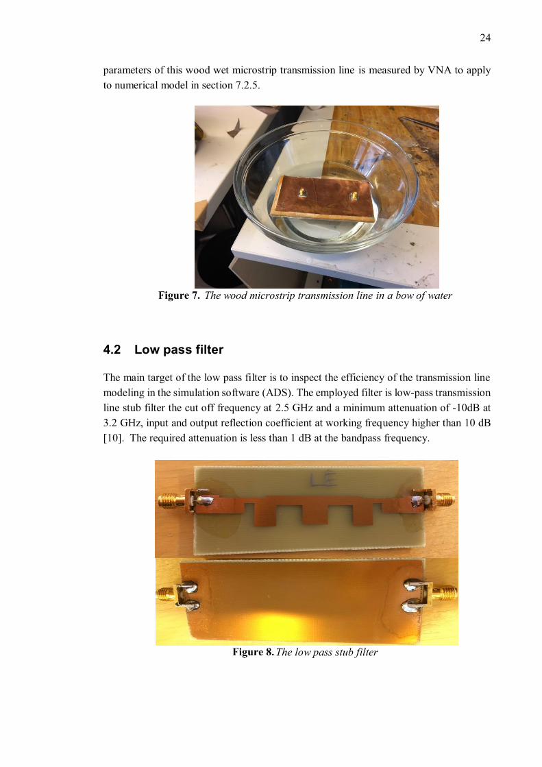
24 parameters of this wood wet microstrip transmission line is measured by VNA to apply to numerical model in section 7.2.5.
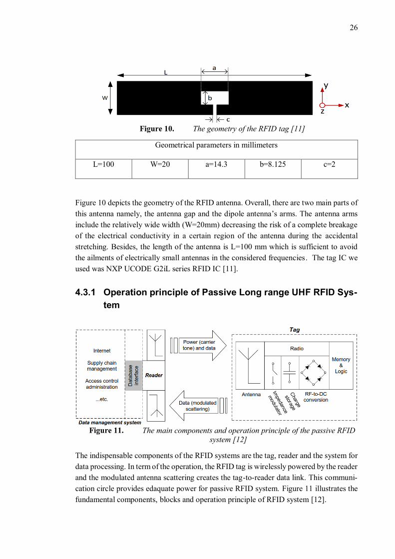
The wood microstrip transmission line in a bow of water 4.2 Low pass filter The main target of the low pass filter is to inspect the efficiency of the transmission line modeling in the simulation software (ADS). The employed filter is low-pass transmission line stub filter the cut off frequency at 2.5 GHz and a minimum attenuation of -10dB at 3.2 GHz, input and output reflection coefficient at working frequency higher than 10 dB [10]. The required attenuation is less than 1 dB at the bandpass frequency.
The low pass stub filter

25 The structure of the low pass stub filter is the maximally flat low-pass prototype. This form of design decreases the ripple of the attenuation level at the pass band frequency [24]. Figure 8 illustrates the practical design of the filter, the FR4 substrate is used and its thickness is 1.6mm. The size of the stub and transmission line is modified based on the permittivity and the loss tangent found in Section 6 of the thesis. Besides, the design is corresponding to the maximally flat low-pass prototype: attenuation the order of the filter can be chosen, N=5 [10]. 4.3 Passive RFID antennas The function of the passive ultra-high frequency radio-frequency identification (UHF RFID) tag demonstrated in Figure 9 is to exam the permittivity and loss tangent of the modeling in section 6 of the thesis [11].
The EPDM cell rubber foam RFID tag The RFID antenna shape is a T-matched dipole which is widely used in antenna config-uration in UHF RFID tags. The design of the antenna composed of the copper tape con-ductor with 42𝜇𝑚 thickness and the EPDM cell rubber foam substrate with 2.5 mm thick-ness. To attach the IC tag to the antenna, the mixing with the equal proportion of conductive epoxy type A and B is used [39]. Besides, the conducting plane is fixed to the substrate area by the available glue in the copper tape addition to the small amount of super glue added at 4 edges of the antenna to avoid the conducting this area sloughing off. To ensure the gel and conductive proxy is completely dry, we need to wait at least four hours with normal condition or we can expose this tag in the oven with 600 C in 20 minutes. Since the author manually constructed the antenna conducting surface by copper tape and attached it to the EPDM cell rubber foam substrate, there are some high roughness in the surface as Figure 9. The roughness of the surface will be taken into account in the model in the simulation software.
26
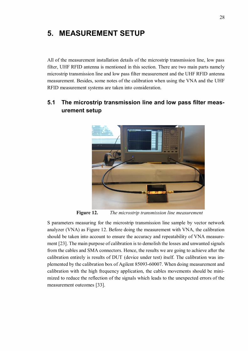
The geometry of the RFID tag [11] Geometrical parameters in millimeters
L=100 W=20 a=14.3 b=8.125 c=2 Figure 10 depicts the geometry of the RFID antenna. Overall, there are two main parts of this antenna namely, the antenna gap and the dipole antenna’s arms. The antenna arms include the relatively wide width (W=20mm) decreasing the risk of a complete breakage of the electrical conductivity in a certain region of the antenna during the accidental stretching. Besides, the length of the antenna is L=100 mm which is sufficient to avoid the ailments of electrically small antennas in the considered frequencies. The tag IC we used was NXP UCODE G2iL series RFID IC [11]. 4.3.1 Operation principle of Passive Long range UHF RFID Sys-tem
The main components and operation principle of the passive RFID system [12] The indispensable components of the RFID systems are the tag, reader and the system for data processing. In term of the operation, the RFID tag is wirelessly powered by the reader and the modulated antenna scattering creates the tag-to-reader data link. This communi-cation circle provides edaquate power for passive RFID system. Figure 11 illustrates the fundamental components, blocks and operation principle of RFID system [12].

27 The tag antenna and the RFID tag microchips (tag ) IC are two main entities of a passive tag. The antenna is in charge of capturing the energy from the continuous wave emitted by the reader and sending the response from the IC tags. When the antenna receives suf-ficient power to activate the semiconductor components and on-chip rectifier circuity, the memory and logic block are initiated. With the tag IC completely activated, IC chip re-ceiving the command the reader. The reader is able to request new data to be saved in the IC tag memory. Normally, the reader scans and receives the stored identification code in the IC chip memory. The responding from the tag is based on modulation the requested data from the tag antenna with impedance matching scheme. When the response is ob-served by the reader, the data supervisor system will manage and process this data [12].
28 5. MEASUREMENT SETUP All of the measurement installation details of the microstrip transmission line, low pass filter, UHF RFID antenna is mentioned in this section. There are two main parts namely microstrip transmission line and low pass filter measurement and the UHF RFID antenna measurement. Besides, some notes of the calibration when using the VNA and the UHF RFID measurement systems are taken into consideration. 5.1 The microstrip transmission line and low pass filter meas-urement setup
The microstrip transmission line measurement S parameters measuring for the microstrip transmission line sample by vector network analyzer (VNA) as Figure 12. Before doing the measurement with VNA, the calibration should be taken into account to ensure the accuracy and repeatability of VNA measure-ment [23]. The main purpose of calibration is to demolish the losses and unwanted signals from the cables and SMA connectors. Hence, the results we are going to achieve after the calibration entirely is results of DUT (device under test) itself. The calibration was im-plemented by the calibration box of Agilent 85093-60007. When doing measurement and calibration with the high frequency application, the cables movements should be mini-mized to reduce the reflection of the signals which leads to the unexpected errors of the measurement outcomes [33].

29
The low pass stub filter measurement The measurement installation of the low pass filter is showed at Figure 13. Similar to the transmission line measurement setup, the input and output of the low pass filter was con-nected to two ports of VNA. After that, the attenuation and reflection coefficient was automatically measured and saved. 5.2 The passive UHF RFID antenna measurement The read range measurement of the UHF RFID antennas was implemented in the RFID tag measurement system in Figure 14.
The antenna measuring system [31]
30 The UHF RFID antenna measurement system contains three main crucial parts which are controlling and monitoring PC (personal computer), Tagformance Pro and the ane-choic chamber [31]. The computer sufficiently provides the users the data and graphs of the transmitting power from RFID reader antenna , transmitted power and backscattered power of RFID tag and RFID tag radiation pattern. From these data, it is able to calculate the details of theoretical forward and reverse read range which are the key parameters of the RFID tags. Besides, it controls the step motors to rotate the RFID tag antenna 3600 in order to measure the radiation pattern of the antenna. The second part of the system is the Tagformance Pro connecting the PC to the anechoic chamber. It delivers the transmitting power and measured the amount of receiving power from the RFID reader antenna [32].
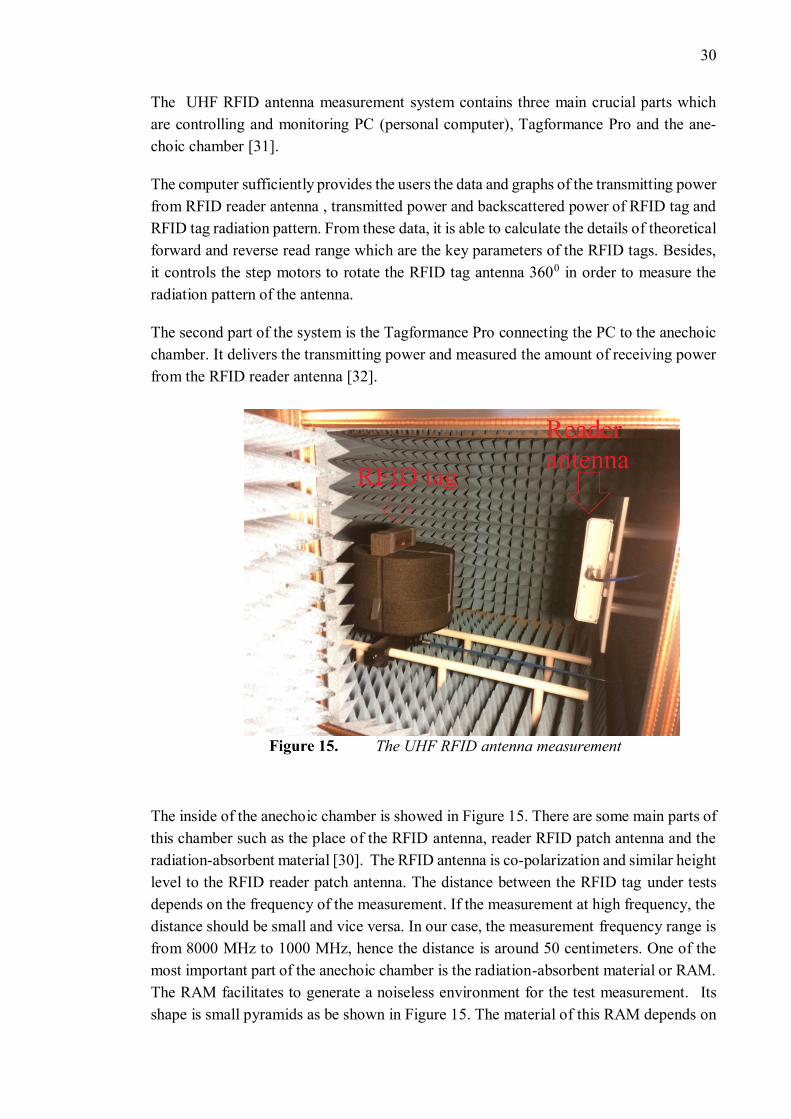
The UHF RFID antenna measurement The inside of the anechoic chamber is showed in Figure 15. There are some main parts of this chamber such as the place of the RFID antenna, reader RFID patch antenna and the radiation-absorbent material [30]. The RFID antenna is co-polarization and similar height level to the RFID reader patch antenna. The distance between the RFID tag under tests depends on the frequency of the measurement. If the measurement at high frequency, the distance should be small and vice versa. In our case, the measurement frequency range is from 8000 MHz to 1000 MHz, hence the distance is around 50 centimeters. One of the most important part of the anechoic chamber is the radiation-absorbent material or RAM. The RAM facilitates to generate a noiseless environment for the test measurement. Its shape is small pyramids as be shown in Figure 15. The material of this RAM depends on

31 the measurement application. In our case, RAM made by impregnating rubberized insu-lating foam with a conductible metal, such as iron. The main purpose of the RAM is to entirely eliminate the reflections of sounds or electromagnetic waves [19]. Hence, there are only the transmitting power from the RFID reader antenna to the RFID antennas and the receiving power from the RFID tags to the RFID reader antenna. In term of measurement principle, the computer sends a signal to tagformance and it sends the a mount of power to the RFID read patch antenna and then amount of power from the patch antenna transmitted to the RFID tag [26]. The transmitted power should be enough to wake up the IC tag. After that, the RFID tag responses a small amount of power to the reader antenna. Basing on the transmitted and received radiation power, the computer can convert to the read range forward and reverse of the RFID antennas. The measurement procedures of RFID antennas include 2 crucial steps [32]. First of all, the calibration with the reference antenna- Voyantic Ltd wideband UHF reference tag v1 should be conducted. Similar to VNA, the calibration for RFID tag measurement dimin-ishes the noise from cables connecting the RFID reader antenna to computer, the noise from the distance between the reader antenna and the tag antenna and the small unwanted signal inside of the anechoic chamber. Secondly, positioning the AUT (antenna under test) inside of chamber and measuring. It is noticed that the position and direction of the AUT should be identical to the reference antenna to achieve the precise results. Besides, during conducting measurement, the door of the chamber should be closed to prevent the interference of surrounding signal. 5.3 The surface roughness measurement The optical profilometer is employed to measure the roughness of the conducting surface of the transmission lines as Figure 16.
The roughness measurement of the microstrip line
32
The surface roughness measurement principle
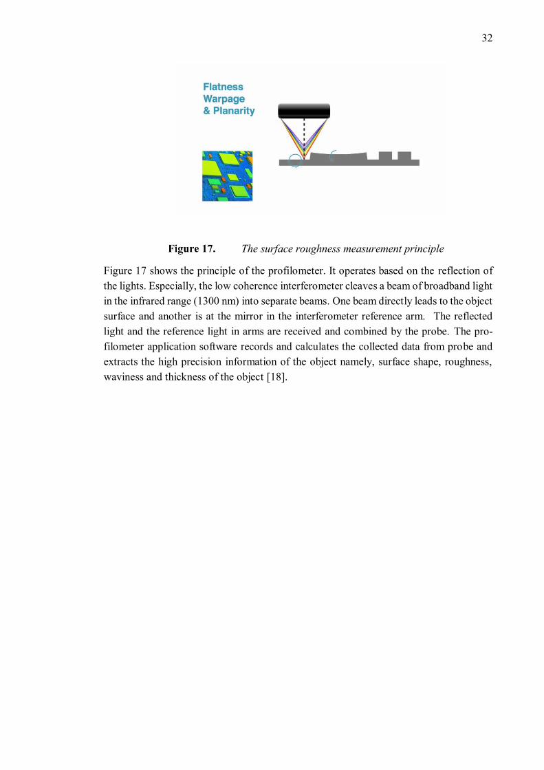
Figure 17 shows the principle of the profilometer. It operates based on the reflection of the lights. Especially, the low coherence interferometer cleaves a beam of broadband light in the infrared range (1300 nm) into separate beams. One beam directly leads to the object surface and another is at the mirror in the interferometer reference arm. The reflected light and the reference light in arms are received and combined by the probe. The pro-filometer application software records and calculates the collected data from probe and extracts the high precision information of the object namely, surface shape, roughness, waviness and thickness of the object [18].

33 6. THE SIMULATION MODEL In this section, there are two main parts which are selecting the solver or simulation soft-ware and designing the model structures. In the first part, the writer shows the appropriate simulation software for each type of model and forms of outcomes of them. In the next parts, some simulation model structures are illustrated such as the microstrip lines, low pass stub filter and UHF RFID antennas. 6.1 Choosing the solver To model the transmission line and low pass filter, ADS (Advanced Design System) and ANSYS Electronics HFSS 2016 were employed to model the RFID antenna. These mod-eling software were chosen because of the tunability of some crucial parameters of the substrate materials such as conductivity, permittivity and loss tangent and the roughness of the surface was also simulated in these software. ADS is based on numerical models of transmission line components whereas HFSS is full-wave electromagnetic field solver based on the finite element method. Besides, ADS enables to sweep the parameters to search out the fitting values between the modeling results in simulation software and the results from measurements by the least square method. On the other hands, ANSYS Elec-tronics 2016 is able to illustrate the theoretical forward read range, radiation pattern of near and far field of antenna if the RFID tags. Both of these software are able to simulate various type of materials for the conductor and the substrate required for the finding per-mittivity and loss tangent. 6.2 The simulation model structures The model structures include the transmission lines, low pass stub filter and the UHF RFID antennas. Firstly, the transmission line is modeled by ADS software. The simula-tion results of each transmission line will be compared to the corresponding measurement results (maximum attainable power gain, relative permittivity and the loss tangent) of practical lines to single out the fitting data, after that the final permittivity and loss tangent are computed. Secondly, in order to assess the accuracy of the numerical model, the found permittivity and loss tangent were applied to the low pass filter and the UHF RFID an-tenna model design. After then, the outcomes of model are compared to the practical measurements.

34 6.2.1 Transmission line model The main purpose of this modeling is to sweep the relative permittivity and the loss tan-gent corresponding to extract maximum attainable power gain. After that we can compare and select the best fit data between the maximum attainable power gain of the measure-ment results and the those of numerical modeling.
The microstrip line model Figure 18 demonstrates the microstrip line model. The microstrip line TL1 has the length is 8 cm and the width is 1 cm which is identical to the practical lines in Section 4.1. The line segments TL2 and TL3 are the model of the connection of the SMA connector and the microstrip line. Term 1 and Term 2 are the SMA connectors. Msub is the block con-sisting of the substrate properties and the conductivity of conductor. In this model, the thickness of substrate is H=2 mm, the relative permeability is 1, conductivity Cond is 58e6 (copper conductivity= 58.106 S/meter, the cover height Hu = 1.0e+ 033mm, the conductor thickness T=35 µm, the permittivity Er is swept from 1.05 to 3, the loss tangent TanD is swept from 0.03 to 0.06. The roughness (Rough=2 µm) is identical to the actual roughness measurement in section 6. Figure 19 shows the simulation result of the constructed microstrip line model which is the maximum attainable power gain versus frequency. The maximum attainable power gain or the attenuation of the transmission line in this figure is the consequence of the sweep of the permittivity (from 1.05 to 3) and loss tangent from 0.03 to 0.06.

35
The maximum attainable power gain versus frequency The maximum attainable power gain tends to decrease along frequency range from 0.4 MHz to 3 GHz. The decreasing of the maximum attainable power gain relatively depends on the permittivity and loss tangent. If the material of the substrate possesses high relative permittivity and loss tangent, the maximum attainable power gain will show the dramatic decreasing or the attenuation will increase [40].
The swept S11 and S21 of the transmission line simulation model The S11 and S21 of the transmission line model are swept as Figure 20. There are 29 values from 1.05 to 3 of the relative permittivity and 32 values of the loss tangent from 0.03 to 0.06. As the results, there are 29*32=928 values in the total of the S21 and S11 which are swept. After that, these swept values were exported and compared to the meas-urement results of the implemented transmission line. The closest value between meas-urement and the simulation model was chosen by the least square estimation method.

36 6.2.2 The low pass filter model The schematic of the 5th order low pass microstrip stub filter is represented in Figure 21. The purpose of the low pass filter is to evaluate the results of the model. The low pass filter is made by the FR4 substrate and pre-printed conducting planes. In term of the de-sign of the model, the permittivity, loss tangent and the roughness of the low pass filter model is identical to those found in section 7.2.1. The filter is modeled at frequency range from 0.4 GHz to 5 GHz [10]. There are various components in the low pass filter model as Figure 21 namely, TEE ( the tee junction), TL (transmission line) and TERM (termi-nator) in the simulation. The dimension of transmission line stubs is manually calculated, optimized and tuned by software in order to reduce the attenuation and increase the performance of the filter. As a consequence, the low pass filter is achieved positive results in simulation as well as manufacturing which is illustrated in Section 6.
The schematic of low pass stub filter simulation model The numerical model outcomes are satisfied when the simulation model results are close to the practical measurement results at desired frequency range (0.4 MHz to 5GHz).
The layout of the low pass filter Figure 22 demonstrates the PCB layout of the low-pass transmission line stub filter, the size of the layout is (7.7 mm*1.3 mm). This layout was printed and etched to generate the PCB board. Finally, the SMA connectors is attached at two sides of the filter to facilitate the measurement process with the VNA (vector network analyser).
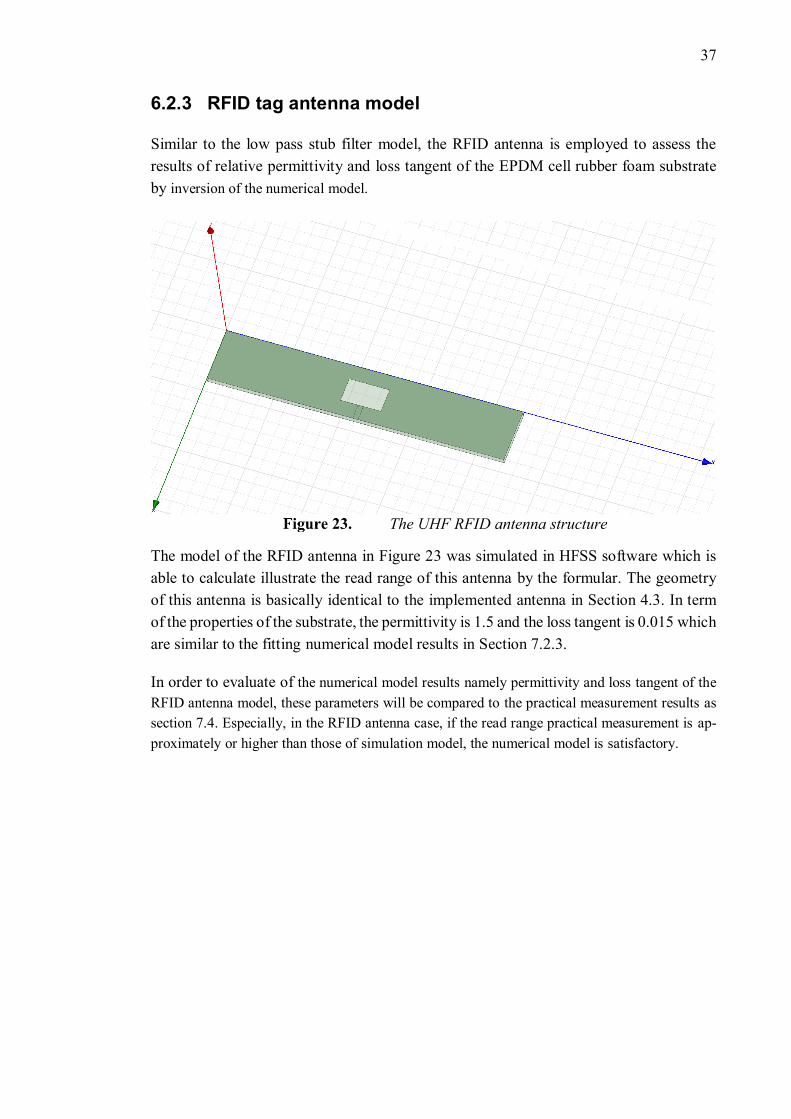
37 6.2.3 RFID tag antenna model Similar to the low pass stub filter model, the RFID antenna is employed to assess the results of relative permittivity and loss tangent of the EPDM cell rubber foam substrate by inversion of the numerical model.
The UHF RFID antenna structure The model of the RFID antenna in Figure 23 was simulated in HFSS software which is able to calculate illustrate the read range of this antenna by the formular. The geometry of this antenna is basically identical to the implemented antenna in Section 4.3. In term of the properties of the substrate, the permittivity is 1.5 and the loss tangent is 0.015 which are similar to the fitting numerical model results in Section 7.2.3. In order to evaluate of the numerical model results namely permittivity and loss tangent of the RFID antenna model, these parameters will be compared to the practical measurement results as section 7.4. Especially, in the RFID antenna case, if the read range practical measurement is ap-proximately or higher than those of simulation model, the numerical model is satisfactory.

38 7. MEASUREMENT RESULTS After constructing and doing the measurement with the real and model of the microstrip transmission lines, low pass filter and the UHF RFID antennas. The measurement results should be cautiously analyzed. There are three main forms of outcomes such as the sur-face roughness of conducting surface, S parameters and the forward theoretical read range. Especially, the conducting surface roughness all of the microstrip transmission lines were conscientiously measured by the profiloromenter and the data of surface rough-ness was inserted to the simulation model of the transmission lines to make this model as similar to the practical condition as possible. Secondly, the key values tell us the characteristic of the transmission line or the substrate of this transmission line which are S parameters. It was automatically measured by VNA. From S parameters, the maximum attainable power gain of the transmission lines was compared to those of the numerical model and the best fit data between them was selected and then the relative permittivity and the loss tangent were calculated basing on this data. The calculated relative permittivity and loss tangent of the FR4 and AR 1000 substrate were weighed up to the data in the datasheet. By this way we can evaluate the accuracy the calculated relative permittivity and loss tangent and calculation of the transmission line model. The next steps is to characterize the unknown relative permittivity and loss tangent materials namely wood, EPDM cell rubber foam and the wood wet at high fre-quency range (400 MHz to 3 GHz). It is noted that the purpose of the wood wet measure-ment is to check the changing of the relative permittivity and loss tangent when the mois-ture of the substrate increases. Thirdly, the result analyzing of the low pass stub filter is taken into account. Especially, the reflection coefficient and the attenuation will be concentrated in this section. Addi-tionally, the collation of the measurement result and the numerical model outcome is de-picted to exam the accuracy of the numerical model. Finally, the comparison outcomes between the practical UHF RFID tag antenna read range and those of model is demonstrated in the last part of this section. The main idea of this comparison is to assess the accuracy of the antenna numerical model in the EPDM cell rubber foam UHF RFID antenna design.

39 7.1 Surface roughness measurement The roughness measurement of the transmission line is indispensable which will be in-serted to the simulation model. The surface roughness measurement was conducted by Veeco's optical profiler with vertical scanning interferometry (VSI) mode which is able to measure a large range of surfaces and larger height discontinuities. VSI is an extremely versatile and satisfactory mode, since it can measure the full range of most surfaces such as integrated circuit boards, paper, fabric or foam [13].
Roughness measuring data of FR4 The sample result of surface roughness measurement of FR4 transmission line in Figure 24. It can be seen that the surface roughness is rough and unstable. It probably affects to the measurement result of S parameters of this transmission line. Besides, the surface statics of the FR4 transmission line are comprehensibly illustrated. The roughness aver-age (Ra) is 744.26 nm, root mean square (rms) roughness Rq=922.07 nm, average maxi-mum height of the profile Rz is 7.81 um and Rt maximum height of the profile is 9.8 um. In the above roughness measurement data, we can insert the root mean square (rms) roughness Rq into the transmission line simulation model in the ADS software [25].

40
Table 1. The roughness measurement data of different transmission lines with different substrate materials
The roughness measurement data of the microstrip line corresponding to different sub-strate materials namely FR4, AR1000,wood and EPDM cell rubber foam are exemplified in Table 2. Based on these data, it is obvious that the FR4 and AR1000 transmission line made by etching technique shows less roughness than those manually made. On the other hands, the surface of the EPDM cell rubber foam is stretchable and flexible, thus root mean square (rms) roughness is dramatically high which is 13 µm. On top of that, the pre-acttached copper conductor is unavailable on the wood and EPDM cell rubber foam sub-strate, hence, the copper tape is required to be manually attached on these substrates as the conductor. Due to this reason, there are some tiny air bubbles exist between the sub-strate surface and copper conductor which increase the surface roughness of the mi-crostrip line.
Material Rq (µm) Ra (µm) Rz (µm) Rt (µm) FR4 1 0.8 19 36.6
AR1000 1 0.744 7.81 9.88 Wood 2.5 1.75 43.92 47.71
EPDM cell rubber foam 13 10.62 66.04 68.89

41 7.2 Microstrip lines results analyzing A wide range of microstrip transmission lines with different substrate materials are meas-ured and its results are critically analyzed in this section. Firstly, the transmission lines made by the FR4 and AR1000 play as the reference to check the accuracy of the outcomes namely, the relative permittivity and loss tangent by comparing with the data from man-ufacturers or datasheet. Secondly, the analyzing results of the EPDM cell rubber foam, wood and wood wet microstrip lines are shown. 7.2.1 FR4 microstrip line The microstrip line measurement is started with the FR4 transmission line. The S param-eters comparison are depicted in Figure 25. Overall, the results of the simulation model S parameters are in close proximity those of the practical measurement results.
The S parameters comparison between simulation model and meas-urement results
Especially, basing on the above graph, basically the S11 and S22 practical measurement (read and blue line) are quite close to those of the simulation model (yellow line).The attenuation of the model and practical transmission line is higher than -15 dB at the whole range of frequency from 0.4 GHz to 3 GHz. The lowest value of the simulation model and practical measurement S11 is approximately -75 dB However, the corresponding fre-quency point of these value is 0.5 GHz different.
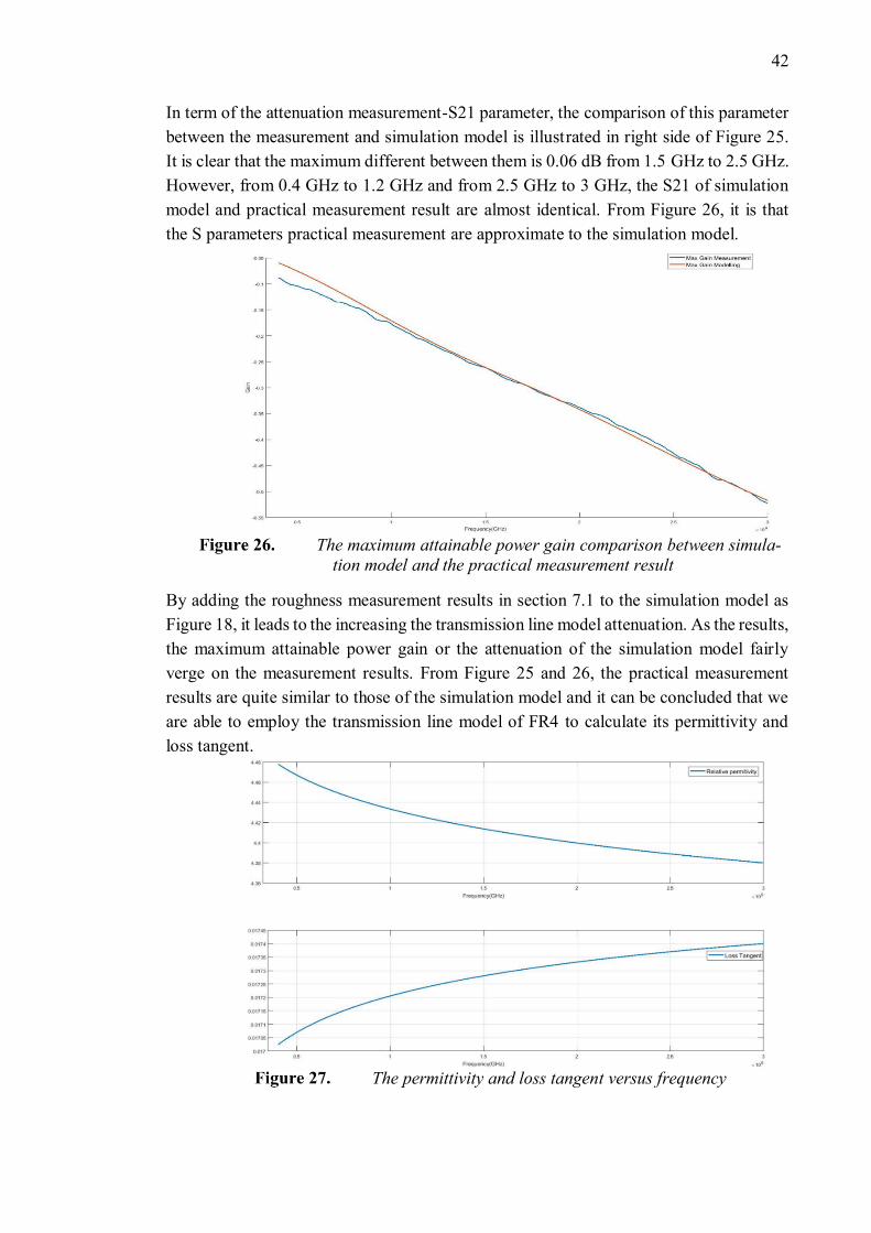
42 In term of the attenuation measurement-S21 parameter, the comparison of this parameter between the measurement and simulation model is illustrated in right side of Figure 25. It is clear that the maximum different between them is 0.06 dB from 1.5 GHz to 2.5 GHz. However, from 0.4 GHz to 1.2 GHz and from 2.5 GHz to 3 GHz, the S21 of simulation model and practical measurement result are almost identical. From Figure 26, it is that the S parameters practical measurement are approximate to the simulation model.
The maximum attainable power gain comparison between simula-tion model and the practical measurement result By adding the roughness measurement results in section 7.1 to the simulation model as Figure 18, it leads to the increasing the transmission line model attenuation. As the results, the maximum attainable power gain or the attenuation of the simulation model fairly verge on the measurement results. From Figure 25 and 26, the practical measurement results are quite similar to those of the simulation model and it can be concluded that we are able to employ the transmission line model of FR4 to calculate its permittivity and loss tangent.
The permittivity and loss tangent versus frequency

43 Figure 27 demonstrates the permittivity and loss tangent of the simulation model. The loss tangent decreases from 4.48 at 0.4 GHz to 4.38 at 3 GHz and the loss tangent is approximately 0.0174 at the whole range of desired frequency (0.4 GHz to 3 GHz). The value of the relative permittivity and loss tangent are quite losing to those in the datasheet data which are 4.7 and 0.014 respectively [14]. From the comparison of the S parameters and maximum attainable power gain, the practical simulation model results are quite sim-ilar to those of measurement. Additionally, from the relative similarity of the permittivity and loss tangent of the model and the datasheet data, it can be concluded that we are able to employ the transmission line model of FR4 substrate to the low pass filter design. 7.2.2 AR 1000 microstrip line AR1000 is another reference material in order to evaluate the accuracy of the transmission line simulation model. Similar to FR4 substrate, the measured S parameters and maxi-mum attainable power gain of the microstrip line of AR1000 substrate are compared those of the simulation model. Finally, the relative permittivity and loss tangent are calculated and compared to the datasheet.
The S parameters comparison between simulation model and meas-urement results of AR1000 substrate As can be seen in Figure 28, the S parameters of the measured results are almost equal to those of simulation model. Especially, both measured and simulation model S11 and S22 results show the resonant frequency at 0.6 GHz, 1.4 GHz, 2 GHz and 2.6 GHz. Besides, the highest reflection coefficient of two kinds of results is around 3 dB. In term of S21 and S12, the measured and simulation model express an almost identical form. Especially, both measured and simulation model results steadily fluctuate from -6 dB to -0.3 dB at the whole range frequency. There are some dramatically decreasing at 1 GHz, 1.7 GHz, 2.3 GHz and 3 GHz due to the resonant frequency of the transmission line.
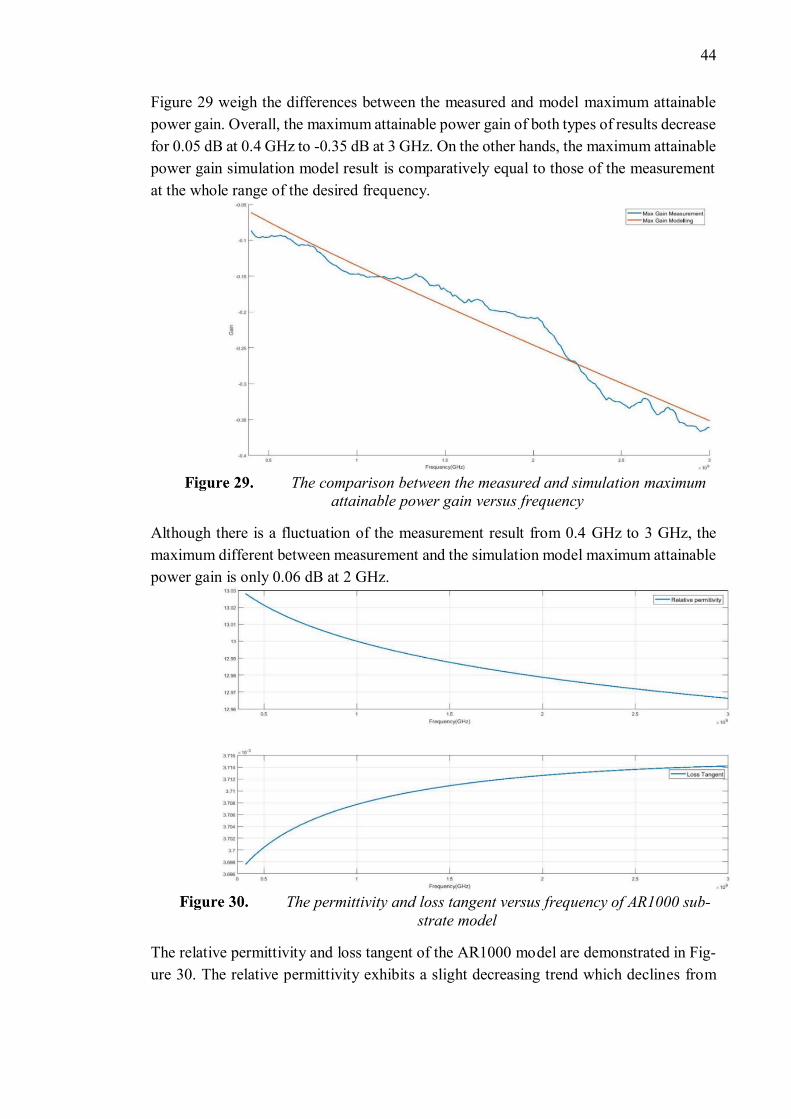
44 Figure 29 weigh the differences between the measured and model maximum attainable power gain. Overall, the maximum attainable power gain of both types of results decrease for 0.05 dB at 0.4 GHz to -0.35 dB at 3 GHz. On the other hands, the maximum attainable power gain simulation model result is comparatively equal to those of the measurement at the whole range of the desired frequency.
The comparison between the measured and simulation maximum attainable power gain versus frequency Although there is a fluctuation of the measurement result from 0.4 GHz to 3 GHz, the maximum different between measurement and the simulation model maximum attainable power gain is only 0.06 dB at 2 GHz.
The permittivity and loss tangent versus frequency of AR1000 sub-strate model The relative permittivity and loss tangent of the AR1000 model are demonstrated in Fig-ure 30. The relative permittivity exhibits a slight decreasing trend which declines from
45 13.03 to 12.97. It is comparable to those in datasheet (approximate 10 depending on thick-ness of the substrate). The loss tangent of the model is around 3.7*10-3 which almost equal to those of datasheet 3.5*10-3. From comparison of the S parameters, maximum attainable power gain, loss tangent and relative permittivity above, almost the simulation model parameter is relatively close to the measurement one and the datasheet [15].
Table 2. The relative permittivity and loss tangent basing on the numerical model of FR4 and AR1000
Table 3 illustrates the collation of the relative permittivity and loss tangent between the model results and data from the datasheet. It can be seen that the model relative permit-tivity and loss tangent provides the results the almost identical to those from the manu-facturers. It can be concluded that the numerical model in the simulation software is sat-isfied to find the relative permittivity and loss tangent of other materials. 7.2.3 EPDM cell rubber foam microstrip line The main purpose of EPDM cell rubber foam microstrip line is to search out the relative permittivity and loss tangent of EPDM cell rubber foam material in order to apply to design the UHF RFID antennas. As be shown in Figure 31, the microstrip line model S11 and S22 graphs are almost sim-ilar to those of the measurement. At 1.7 GHz, the S11 of modeling is lower than those of model 20 dB. However, since S11 and S22 of model and measurement are lower than -30 dB, hence the difference between them are insignificant. The S21 and S12 of the meas-urement results fluctuate at the whole range of frequency due to the high surface rough-ness of the conductor and substrate.
Substrate material
Relative permittivity Loss tangent Model Datasheet Model Datasheet
FR4 4.42 4.3-4.7 0.01725 0.017 AR100 12.99 10-13 0.00371 0.003

46
The comparison of S parameters between measurement and model of EPDM cell rubber foam microstrip line
Nevertheless, these value of the measurement are not far from those of microstrips line model on the simulation software. The maximum dissimilarity is around 0.05 dB from 2.5 GHz to 3 GHz.
The comparison between the measurement and model maximum at-tainable power gain of the EPDM cell rubber foam transmission line

47 The maximum attainable power gain of the microstrip line model (read line) is approxi-mate to the maximum attainable power gain of the measurement as Figure 32. To be more specific, from 0.4 GHz to 2.4 GHz, there is a decreasing trend in the maximum attainable power gain of both measurement and model from -0.05 to -0.2. The measurement maxi-mum attainable power gain possesses some variation at above 2.5 GHz. The maximum distinction between measurement and model maximum attainable power gain is 0.15 from 2.7 GHz to 3 GHz because of the instability of the conducting, substrate surface and cable connection.
The permittivity and loss tangent of the EPDM cell rubber foam substrate model After comparing the S parameters and the maximum attainable power gain between the measurement and model results, the relative permittivity and loss tangent of the EPDM cell rubber foam substrate is computed. As Figure 33, the relative permittivity slightly falls from 1.55 to 1.52. By contrast, the loss tangent sees a slight rise from 0.0137 to approximately to 0.014. Since the reference values of the permittivity and loss tangent are unavailable, hence the author of this thesis implemented the UHF RFID tags and did the measurement in order to evaluate the accuracy of the EPDM cell rubber foam model. The evaluation is shown in section 7.4. 7.2.4 Wood microstrip line This part demonstrates the found relative permittivity and loss tangent of the wood with 3mm thickness by the numerical model of the microstrip line. First of all, the S parameters of the model is compared to those of the practical measurement as Figure 34.

48
The S parameters comparison between the measurement and model of wood microstrip line In general, it can be seen that the fluctuation exists in S11, S22, S21 and S12 measurement and the model wood microstrip transmission line. Especially, both S11 and S22 of meas-urement and model results show the lowest value (approximate -30 dB) at around 1GHz. While the second lowest reflection coefficient (S11) of the model is -30 dB at 1.8 GHz and those of the practical measurement is -26 dB at above 2 GHz. The main reason for this difference may be from the instability of the roughness of the conducting surface of the practically implemented wood transmission line. In term of S21 and S12 comparison, both measurement and model outcomes are close to each other’s from 0.4 GHz to 2.4 GHz and both forms of results witness a slight drop from -0.4 dB to -1.5 dB. On the other hands, the measurement attenuation experiences more decreasing to those of model at above 2.5 GHz due to the roughness of the practical transmission line.

49
The permittivity and loss tangent of the wood substrate model The outcomes of the maximum attainable power gain of both measurement and model is depicted in Figure 35. Generally, although there is negligible variation, the value of the maximum attainable power gain of the model are almost equal to those of the measure-ment result which show a decreasing trend from -0.1 dB at 0.4 GHz to -1.4 GHz at 3 GHz.
The maximum attainable power gain result comparison between measurement and model versus frequency As can be seen from the above graph, the relative permittivity of the wood substrate varies from 5.4 to 5.2 at 0.4 GHz and 3 GHz respectively. While the loss tangent undergoes an

50 insignificant increasing trend from 0.0346 to 0.0364 at 0.4 GHz and 3 GHz in that order. Comparing to previous research, the found permittivity is in range of the reference value which is from 2 to 6 [16]. The relative permittivity and loss tangent of the wood substrate model. 7.2.5 Wood wet microstrip line The wood wet microstrip line was implemented to exam the modification of the relative permittivity and loss tangent of the permeable materials. The author hypothesis is that when the wood substrate turns wet, the relative permittivity and loss tangent will dramat-ically increase.
The S parameters comparison between the measurement and model of the wood wet microstrip line The collation of the wood wet microstrip transmission line measurement and model is expressed at Figure 37. As is illustrated, there is a remarkable dissimilarity between meas-urement and model S22 and S11 parameters. Especially, from 0.4 GHz to 1.4 GHz, the minimum reflection coefficient of the measurement result is 16 dB while those of the model results is around 8 dB. At the higher 1.5 GHz frequency range, the measurement and model reflection coefficient experience the fluctuation from approximately 8 dB to 14 dB. The main reason for the disagreement between the practical measurement and the model reflection coefficient may be that the water not entirely penetrate to the wood strate, hence, there some part of the wood contains a huge amount water and some parts are not. This reason also causes the fluctuation in the reflection coefficient of the practical transmission line. On the other hands, the S21 and S12 or the forward and reverse voltage

51 gain of the transmission line model are interestingly not far from those of the real trans-mission line. Both show a decreasing trend from -1.5 dB to -7.5 dB and the maximum difference between measurement and model is 1 dB at 0.8 GHz.
The maximum attainable power gain result comparison between measurement and model versus frequency of the wood wet transmission line Although there is a fluctuation and different of the measurement and model S11 and S22, the maximum attainable power gain comparison shows a satisfy trend as Figure 38.
The relative permittivity and loss tangent of the wood wet substrate model Especially, it is clear that the maximum attainable power gain of the real measurement is in the vicinity of the model maximum attainable power gain graph. Both outcome data go

52 down from -0.8 to around -7. One of the main reason for the increase of the attenuation of the transmission line is that the water in the wood substrate levels up the relative con-ductivity. The maximum differentiation between the measurement and model maximum attainable power gain is only 0.3 at 0.9 GHz.
53 7.3 Comparing the results of modeling and measurement of low pass filter (FR4) The main target of the FR4 low pass filter is to assess the accuracy of the found relative permittivity and loss tangent which are the results of the numerical model of the trans-mission line in previous section 7.1.2. In order to achieve this goal, the low pass filter model insertion loss and reflection coefficient were weighed up with those of the practical low pass filter measurement. If the results of the model are close to those of the practical measurement, the relative permittivity and loss tangent of the model are satisfied.
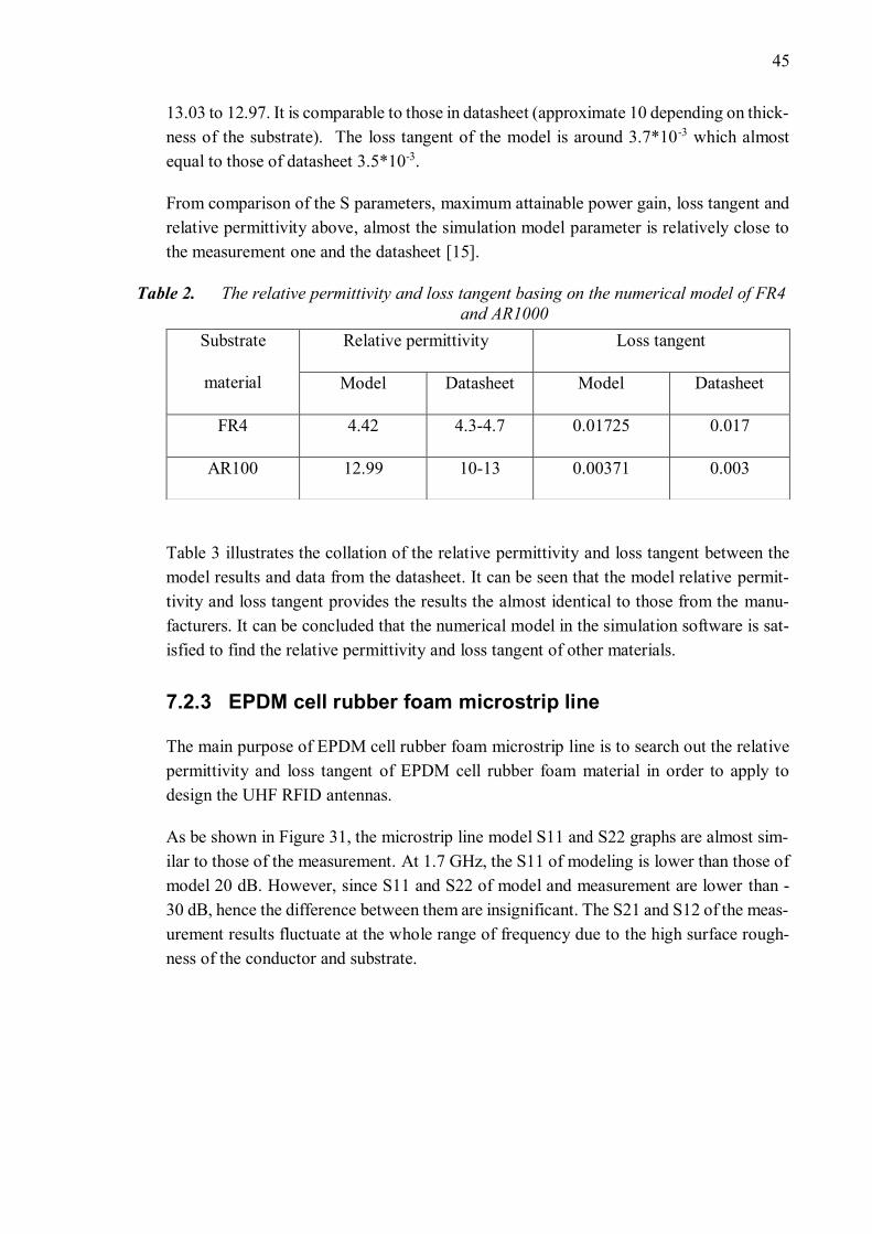
The transducer gain comparison between the model and practical low pass stub filter Figure 40 represents the data of the model and practical low pass filter results. Overall, it is clear that the transducer gain of the low pass filter model is relatively similar to the transducer gain of the practical low pass filter. The most interesting thing is that both practical and the model filter transducer gain undergo the fluctuation from 0.7 to 0.9 of the transducer gain from 0.5 GHz to 2.5 GHz. There are three peaks of the insertion loss of practical and model filter which are 0.9 and 0.7 at 0.9 GHz, 1.5 GHz and 2.3 GHz. The mean value of the transducer gain of the practical and model filter is 0.8 from 0.4 GHz to 2.5 GHz which means around 80% of the signal is transmitted from the input to the output of the low pass filter at the pass band frequency range (0.4 GHz to 2.5 GHz). Additionally, the explanation for the fluctuation is from the conductor roughness (around 1µm for FR4) and the losses of the connecting cables. Since the criteria for the minimum attenuation is the low pass filter is -10 dB at 3.2 GHz, hence after this frequency, the transducer gain of the model and the practical filter is almost equal to zero.
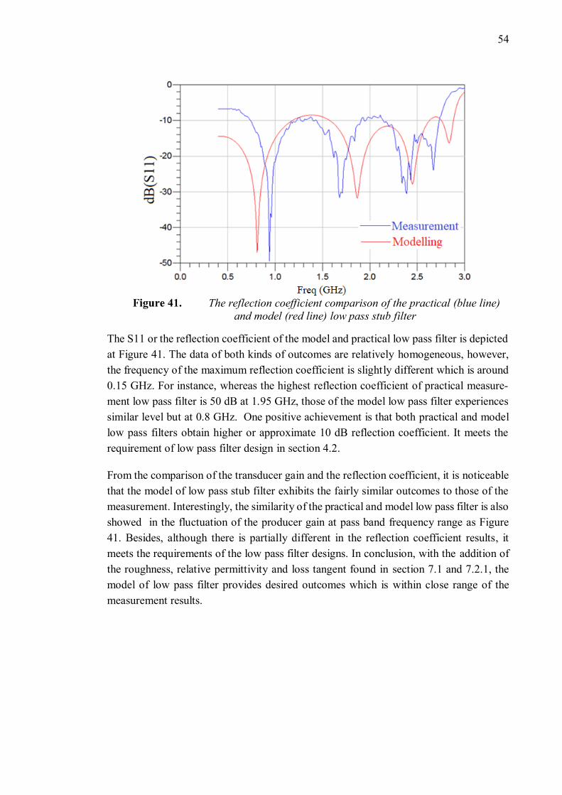
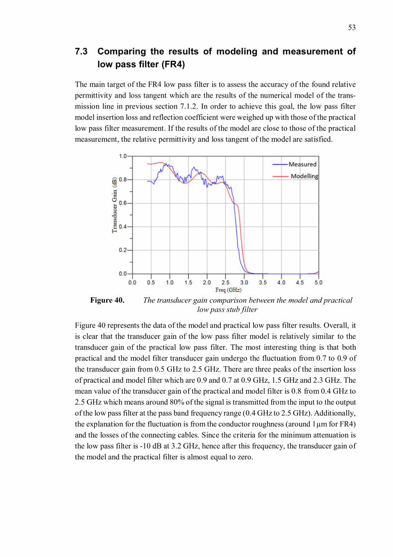
54
The reflection coefficient comparison of the practical (blue line) and model (red line) low pass stub filter The S11 or the reflection coefficient of the model and practical low pass filter is depicted at Figure 41. The data of both kinds of outcomes are relatively homogeneous, however, the frequency of the maximum reflection coefficient is slightly different which is around 0.15 GHz. For instance, whereas the highest reflection coefficient of practical measure-ment low pass filter is 50 dB at 1.95 GHz, those of the model low pass filter experiences similar level but at 0.8 GHz. One positive achievement is that both practical and model low pass filters obtain higher or approximate 10 dB reflection coefficient. It meets the requirement of low pass filter design in section 4.2. From the comparison of the transducer gain and the reflection coefficient, it is noticeable that the model of low pass stub filter exhibits the fairly similar outcomes to those of the measurement. Interestingly, the similarity of the practical and model low pass filter is also showed in the fluctuation of the producer gain at pass band frequency range as Figure 41. Besides, although there is partially different in the reflection coefficient results, it meets the requirements of the low pass filter designs. In conclusion, with the addition of the roughness, relative permittivity and loss tangent found in section 7.1 and 7.2.1, the model of low pass filter provides desired outcomes which is within close range of the measurement results.
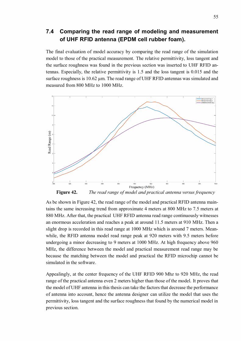
55 7.4 Comparing the read range of modeling and measurement of UHF RFID antenna (EPDM cell rubber foam). The final evaluation of model accuracy by comparing the read range of the simulation model to those of the practical measurement. The relative permittivity, loss tangent and the surface roughness was found in the previous section was inserted to UHF RFID an-tennas. Especially, the relative permittivity is 1.5 and the loss tangent is 0.015 and the surface roughness is 10.62 µm. The read range of UHF RFID antennas was simulated and measured from 800 MHz to 1000 MHz.
The read range of model and practical antenna versus frequency As be shown in Figure 42, the read range of the model and practical RFID antenna main-tains the same increasing trend from approximate 4 meters at 800 MHz to 7.5 meters at 880 MHz. After that, the practical UHF RFID antenna read range continuously witnesses an enormous acceleration and reaches a peak at around 11.5 meters at 910 MHz. Then a slight drop is recorded in this read range at 1000 MHz which is around 7 meters. Mean-while, the RFID antenna model read range peak at 920 meters with 9.5 meters before undergoing a minor decreasing to 9 meters at 1000 MHz. At high frequency above 960 MHz, the difference between the model and practical measurement read range may be because the matching between the model and practical the RFID microchip cannot be simulated in the software. Appealingly, at the center frequency of the UHF RFID 900 Mhz to 920 MHz, the read range of the practical antenna even 2 meters higher than those of the model. It proves that the model of UHF antenna in this thesis can take the factors that decrease the performance of antenna into account, hence the antenna designer can utilize the model that uses the permittivity, loss tangent and the surface roughness that found by the numerical model in previous section.
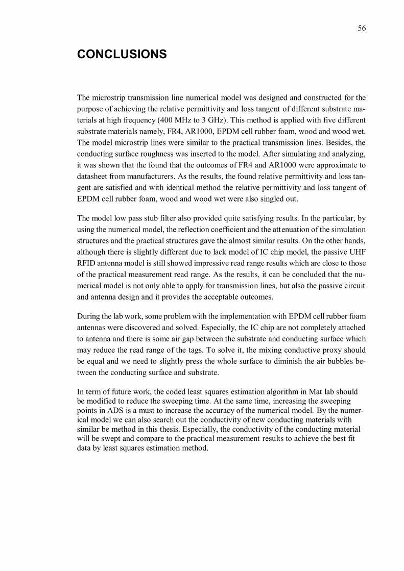
56 CONCLUSIONS The microstrip transmission line numerical model was designed and constructed for the purpose of achieving the relative permittivity and loss tangent of different substrate ma-terials at high frequency (400 MHz to 3 GHz). This method is applied with five different substrate materials namely, FR4, AR1000, EPDM cell rubber foam, wood and wood wet. The model microstrip lines were similar to the practical transmission lines. Besides, the conducting surface roughness was inserted to the model. After simulating and analyzing, it was shown that the found that the outcomes of FR4 and AR1000 were approximate to datasheet from manufacturers. As the results, the found relative permittivity and loss tan-gent are satisfied and with identical method the relative permittivity and loss tangent of EPDM cell rubber foam, wood and wood wet were also singled out. The model low pass stub filter also provided quite satisfying results. In the particular, by using the numerical model, the reflection coefficient and the attenuation of the simulation structures and the practical structures gave the almost similar results. On the other hands, although there is slightly different due to lack model of IC chip model, the passive UHF RFID antenna model is still showed impressive read range results which are close to those of the practical measurement read range. As the results, it can be concluded that the nu-merical model is not only able to apply for transmission lines, but also the passive circuit and antenna design and it provides the acceptable outcomes. During the lab work, some problem with the implementation with EPDM cell rubber foam antennas were discovered and solved. Especially, the IC chip are not completely attached to antenna and there is some air gap between the substrate and conducting surface which may reduce the read range of the tags. To solve it, the mixing conductive proxy should be equal and we need to slightly press the whole surface to diminish the air bubbles be-tween the conducting surface and substrate. In term of future work, the coded least squares estimation algorithm in Mat lab should be modified to reduce the sweeping time. At the same time, increasing the sweeping points in ADS is a must to increase the accuracy of the numerical model. By the numer-ical model we can also search out the conductivity of new conducting materials with similar be method in this thesis. Especially, the conductivity of the conducting material will be swept and compare to the practical measurement results to achieve the best fit data by least squares estimation method.

57 8. REFERENCES [1] Pozar D. Microwave Engineering, Fourth Edition, 2011. Pages:48-51. [2] Tsipogiannis, C. (2012). Microwave materials characterization using waveguides
and coaxial probe. [3] Baker-Jarvis, J. (1990). “Transmission/Reflection and Short-Circuit Line Permit-
tivity Measurements”, NIST Technical Note, National Institute of Standards and
Technology, Bounder, Colorado 80303-3328. [4] Peter b. K. Kyabaggu (2010). Modeling And Characterization Of 3d Multilayer
Transmission Lines. Available Online: https://www.research.manches-ter.ac.uk/portal/files/54596914/FULL_TEXT.PDF.
[5] Rydholm T (2015). Measurement of Complex Permittivity and Permeability Through a Cavity Perturbation Method. Available online: http://www.chalmers.se/en/departments/physics/research/cmt/tassin/Docu-ments/Tomas_Rydholm_Exjobb.pdf.
[6] Bockelman, D. E., & Eisenstadt, W. R. (1995). Combined differential and com-mon-mode scattering parameters: Theory and simulation. IEEE transactions on microwave theory and techniques, 43(7), 1530-1539.
[7] Sara a (2005). Least Squares Estimation. Available online: http://stat.ethz.ch/~geer/bsa199_o.pdf.
[8] Rautio, J. C., & Demir, V. (2003). Microstrip conductor loss models for electro-magnetic analysis. IEEE transactions on microwave theory and techniques, 51(3), 915-921.
[9] Björninen, T., Virkki, J., Sydänheimo, L., & Ukkonen, L. (2014, September). Im-pact of recurrent stretching on the performance of electro-EPDM cell rubber foam UHF RFID tags. In Electronics System-Integration Technology Conference (ESTC), 2014 (pp. 1-5). IEEE.
[10] Björninen, T. Passive RF Circuits – Spring 2017, meeting 1, 2017 [11] Björninen, T., Virkki, J., Sydänheimo, L., & Ukkonen, L. (2014, September). Im-
pact of recurrent stretching on the performance of electro-EPDM cell rubber foam UHF RFID tags. In Electronics System-Integration Technology Conference (ESTC), 2014 (pp. 1-5). IEEE.

58 [12] Björninen, T. (2012). Advances in Antennas, Design Methods and Analysis Tools
for Passive UHF RFID Tags. Tampereen teknillinen yliopisto. Julkaisu-Tampere University of Technology. Publication; 1041.
[13] Optics A (2009). High-Definition Vertical Scanning Interferometry Enables Greater Measurement Detail by Veeco Instruments. Available Online: https://www.azooptics.com/Article.aspx?ArticleID=198.
[14] C.I.F. FR4 Datasheet (2013). Available Online: https://www.far-nell.com/datasheets/1644697.pdf.
[15] Microwave Materials, AR1000 and AR600 (2013). PTFE/Woven Fiberglass/Ce-ramic Filled High Er Laminates. Available Online: http://www.ctsind.com/pdf/AR1000_AR600.pdf.
[16] The Engineering Tollbox (2013). Relative Permittivity - the Dielectric Constant, Some common materials and their relative permittivity. Available Online: https://www.engineeringtoolbox.com/relative-permittivity-d_1660.html.
[17] X Bam (2003). Non-Destructive Testing in Civil Engineering 2003, Non destruc-tive evaluation of concrete moisture by GPR technique: experimental study and direct modeling.
[18] Direct Industry (2010). Surface Characterization and Roughness Measurement. Available Online: http://pdf.directindustry.com/pdf/novacam-technologies-inc/surface-characterization-roughness-measurement/83317-614853.html.
[19] Silva, M. W. B., & Kretly, L. C. (2011, October). A new concept of RAM-Radia-tion Absorbent Material: Applying corrugated surfaces to improve reflectivity. In Microwave & Optoelectronics Conference (IMOC), 2011 SBMO/IEEE MTT-S In-ternational (pp. 556-560). IEEE.
[20] J. Baker-Jarvis, R. G. Geyer, J. H. Grosvenor, Jr.,M. D. Janezic, C. A. Jones, B. Riddle, C. M. Weil, and J. Krupka, “Dielectric characterization of low-loss mate-rials a comparison of techniques,” IEEE Trans. Dielectrics Electrical Insulation,
vol. 5, no. 4, pp. 571-577, Aug. 1998. [21] K. C. Yaw, “Measurement of dielectric material properties: application note,”
Rhode & Schwarz, 04.2012-RAC-0607-0019_1_5E, 2012. [22] L. Chen, C. K. Ong, V. V. Varadan, and V. K. Varadan, Microwave Electronics:
Measurement and Materials Characterization, John Wiley & Sons, Inc., 2004. [23] National Instrument (2013). Vector Network Analyzer Calibration. Available
online: http://www.ni.com/tutorial/14114/en/.

59 [24] Vaghela Himali P, Baraiya Neha G, Raval Falguni et al. MaximallyFlat Low Pass
Filter at 1 GHz. Inventi Rapid: Electronic Components, 2016(1):1-3, 2015.Maxi-mally Flat Low Pass Filter at 1 GHz (PDF Download Available). Available from: https://www.researchgate.net/publication/289433722_Maxi-mally_Flat_Low_Pass_Filter_at_1_GHz [accessed May 23 2018].
[25] Keysight Techonoly (2009). MSUB (Microstrip Substrate). Available Online: http://edadocs.software.keysight.com/pages/viewpage.action?pageId=5259405.
[26] Rabaey, J. M., Mark, M., Chen, D., Sutardja, C., Tang, C., Gowda, S., ... & Werthimer, D. (2011, March). Powering and communicating with mm-size im-plants. In Design, Automation & Test in Europe Conference & Exhibition (DATE), 2011 (pp. 1-6). IEEE.
[27] Yamashita, E., & Mittra, R. (1968). Variational method for the analysis of mi-crostrip lines. IEEE Transactions on Microwave theory and Techniques, 16(4), 251-256.
[28] Browme J (2016). Dielectric Microstrip Lines Achieve Low Loss at THz Frequen-cies. Available online: http://www.mwrf.com/passive-components/dielectric-mi-crostrip-lines-achieve-low-loss-thz-frequencies.
[29] Gonçalves, R., Magueta, R., Pinho, P., & Carvalho, N. B. (2016). Dissipation Fac-tor and Permittivity Estimation of Dielectric Substrates Using a Single Microstrip Line Measurement. Applied Computational Electromagnetics Society Journal, 31(2).
[30] Rudander, J. H., Kildal, P. S., & Orlenius, C. (2011). Measurements of RFID tag sensitivity in reverberation chamber. IEEE Antennas and Wireless Propagation Letters, 10, 1345-1348.
[31] SML RFID (2013). Anechoic Chamber & Tagformance Measurement Set Up. Hardware Testing. Available online: https://sml-rfid.com/products/training-and-testing/hardware-testing/.
[32] EPC global (2008). Tag Performance Parameters and Test Methods Version 1.1.3. Available online: https://www.gs1.org/docs/epc/uhfg2_1_1_0-TestMethod-TagParameters_1_1_3-20080630.pdf.
[33] Tektronix (2017). Improving VNA measurement accuracy with quality cables and adapters. Available online: https://www.tek.com/blog/improving-vna-measure-ment-accuracy-quality-cables-and-adapters.

60 [34] Declercq, F., Rogier, H., & Hertleer, C. (2008). Permittivity and loss tangent char-
acterization for garment antennas based on a new matrix-pencil two-line method. IEEE Transactions on antennas and propagation, 56(8), 2548-2554.
[35] Lunden, O. P (2017). Basic of RF Engineering. Lecture 3. [36] RFcafe (2006). Skin Depth (aka Skin Effect) as a Function of Frequency, Permea-
bility, & Conductivity. Available online: http://www.rfcafe.com/references/elec-trical/skin-depth.htm
[37] Lai, K. C. (2011). Electromagnetic wave propagation in microstrip transmission lines.
[38] Declercq, F., Rogier, H., & Hertleer, C. (2008). Permittivity and loss tangent char-acterization for garment antennas based on a new matrix-pencil two-line method. IEEE Transactions on antennas and propagation, 56(8), 2548-2554.
[39] Chemtronics Technical Data Sheet. 60 Minute Conductive Epoxy TDS CW2460. Available online: http://www.farnell.com/datasheets/1795434.pdf.
[40] Che, W., Tang, Y. F., Zhang, J., & Chow, Y. L. (2010). Formulas of dielectric and total attenuations of a microstrip line. Radio Science, 45(5).

61 APPENDIX A: MATLAB CODE The least squares estimation method was conducted in the matlab which is presented as follow.
Initialize and import measured data clc
close all
clear all
data = read(rfdata.data,'6CML2.98MMW2.2.s2p');
S = data.S_Parameters;
f = data.Freq; %GHz
% Symmetrise S by setting s11 = s22 = mean(s11,s22) and s12 = s21 = mean(s12,s21)
for m = 1:numel(f)
S(:,:,m) = [(S(1,1,m)+S(2,2,m)) (S(1,2,m)+S(2,1,m)); (S(1,2,m)+S(2,1,m))
(S(1,1,m)+S(2,2,m))]/2;
end
if ~ispassive(S)
S = makepassive(S);
disp('S-matrix was made passive')
end
Gma_m = 10*log10(powergain(S,'Gmag')); %Compute maximum attainable gain [dB] from the
measured data.
Nfp = 201; %Number of frequency points in each measurement and simulation (MUST BE
EQUAL).
Nme = 40*24; %Total number of model evaluations in ADS (i.e. the total number of
swept parameter values).
Initialize and import measured data
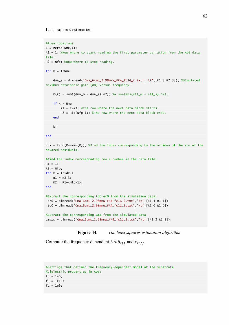
62 Least-squares estimation %Preallocations
E = zeros(Nme,1);
R1 = 1; %Row where to start reading the first parameter variation from the ADS data
file.
R2 = Nfp; %Row where to stop reading.
for k = 1:Nme
Gma_s = dlmread('Gma_6cmL_2.98mmW_FR4_fc1G_2.txt','\t',[R1 3 R2 3]); %SImulated
maximum attainable gain [dB] versus frequency.
E(k) = sum((Gma_m - Gma_s).^2); %+ sum(abs(s11_m - s11_s).^2);
if k < Nme
R1 = R2+3; %The row where the next data block starts.
R2 = R1+(Nfp-1); %The row where the next data block ends.
end
k;
end
idx = find(E==min(E)); %Find the index corresponding to the minimum of the sum of the
squared residuals.
%Find the index corresponding row a number in the data file:
R1 = 1;
R2 = Nfp;
for k = 1:idx-1
R1 = R2+3;
R2 = R1+(Nfp-1);
end
%Extract the corresponding td0 er0 from the simulation data:
er0 = dlmread('Gma_6cmL_2.98mmW_FR4_fc1G_2.txt','\t',[R1 1 R1 1])
td0 = dlmread('Gma_6cmL_2.98mmW_FR4_fc1G_2.txt','\t',[R1 0 R1 0])
%Extract the corresponding Gma from the simulated data
Gma_s = dlmread('Gma_6cmL_2.98mmW_FR4_fc1G_2.txt','\t',[R1 3 R2 3]);
The least squares estimation algorithm Compute the frequency dependent 𝑡𝑎𝑛𝛿𝑒𝑓𝑓 and 휀𝑟𝑒𝑓𝑓 %Settings that defined the frequency-dependent model of the substrate
%dielectric properties in ADS:
fL = 1e6;
fH = 1e12;
fC = 1e9;
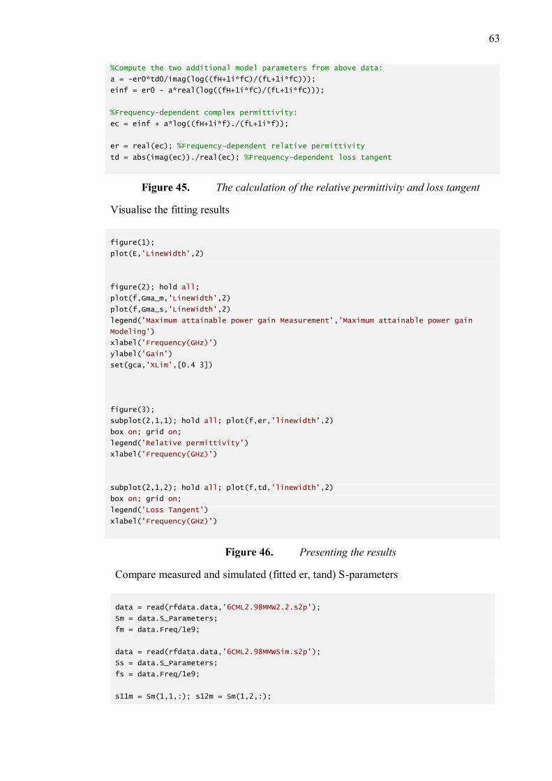
63 %Compute the two additional model parameters from above data:
a = -er0*td0/imag(log((fH+1i*fC)/(fL+1i*fC)));
einf = er0 - a*real(log((fH+1i*fC)/(fL+1i*fC)));
%Frequency-dependent complex permittivity:
ec = einf + a*log((fH+1i*f)./(fL+1i*f));
er = real(ec); %Frequency-dependent relative permittivity
td = abs(imag(ec))./real(ec); %Frequency-dependent loss tangent
The calculation of the relative permittivity and loss tangent Visualise the fitting results figure(1);
plot(E,'LineWidth',2)
figure(2); hold all;
plot(f,Gma_m,'LineWidth',2)
plot(f,Gma_s,'LineWidth',2)
legend('Maximum attainable power gain Measurement','Maximum attainable power gain
Modeling')
xlabel('Frequency(GHz)')
ylabel('Gain')
set(gca,'XLim',[0.4 3])
figure(3);
subplot(2,1,1); hold all; plot(f,er,'linewidth',2)
box on; grid on;
legend('Relative permittivity')
xlabel('Frequency(GHz)')
subplot(2,1,2); hold all; plot(f,td,'linewidth',2)
box on; grid on;
legend('Loss Tangent')
xlabel('Frequency(GHz)')
Presenting the results Compare measured and simulated (fitted er, tand) S-parameters data = read(rfdata.data,'6CML2.98MMW2.2.s2p');
Sm = data.S_Parameters;
fm = data.Freq/1e9;
data = read(rfdata.data,'6CML2.98MMWSim.s2p');
Ss = data.S_Parameters;
fs = data.Freq/1e9;
s11m = Sm(1,1,:); s12m = Sm(1,2,:);
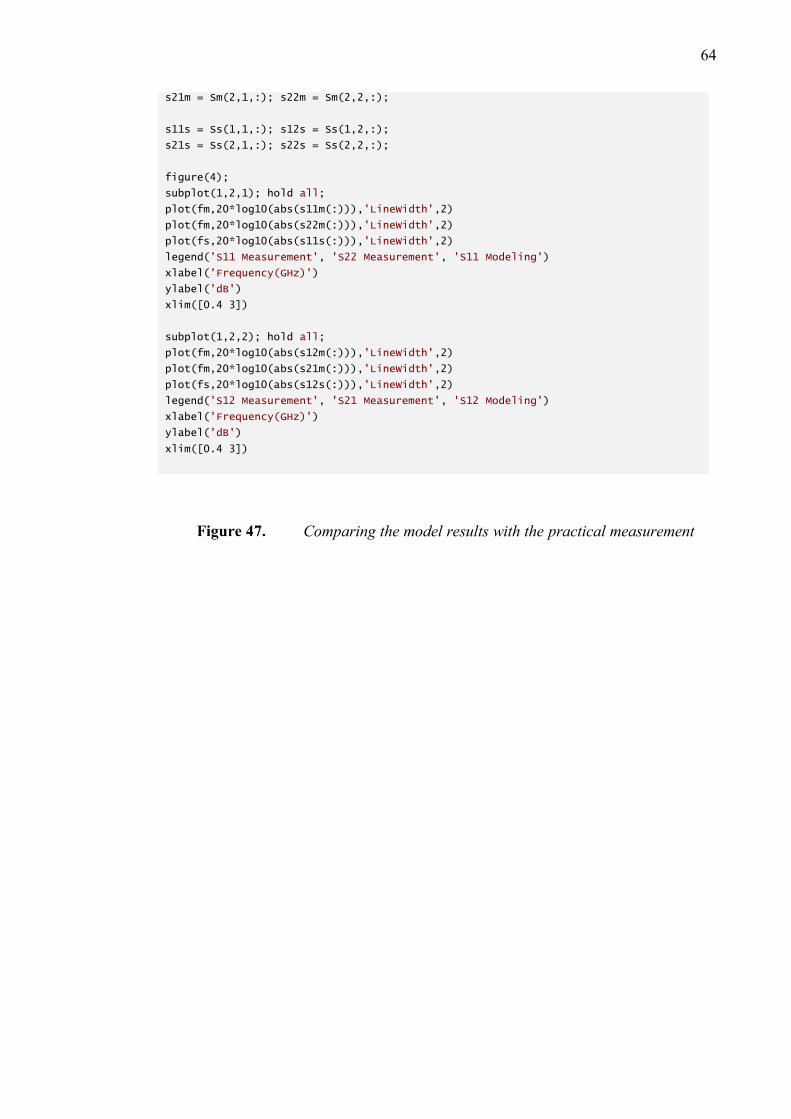
64 s21m = Sm(2,1,:); s22m = Sm(2,2,:);
s11s = Ss(1,1,:); s12s = Ss(1,2,:);
s21s = Ss(2,1,:); s22s = Ss(2,2,:);
figure(4);
subplot(1,2,1); hold all;
plot(fm,20*log10(abs(s11m(:))),'LineWidth',2)
plot(fm,20*log10(abs(s22m(:))),'LineWidth',2)
plot(fs,20*log10(abs(s11s(:))),'LineWidth',2)
legend('S11 Measurement', 'S22 Measurement', 'S11 Modeling')
xlabel('Frequency(GHz)')
ylabel('dB')
xlim([0.4 3])
subplot(1,2,2); hold all;
plot(fm,20*log10(abs(s12m(:))),'LineWidth',2)
plot(fm,20*log10(abs(s21m(:))),'LineWidth',2)
plot(fs,20*log10(abs(s12s(:))),'LineWidth',2)
legend('S12 Measurement', 'S21 Measurement', 'S12 Modeling')
xlabel('Frequency(GHz)')
ylabel('dB')
xlim([0.4 3])
Comparing the model results with the practical measurement
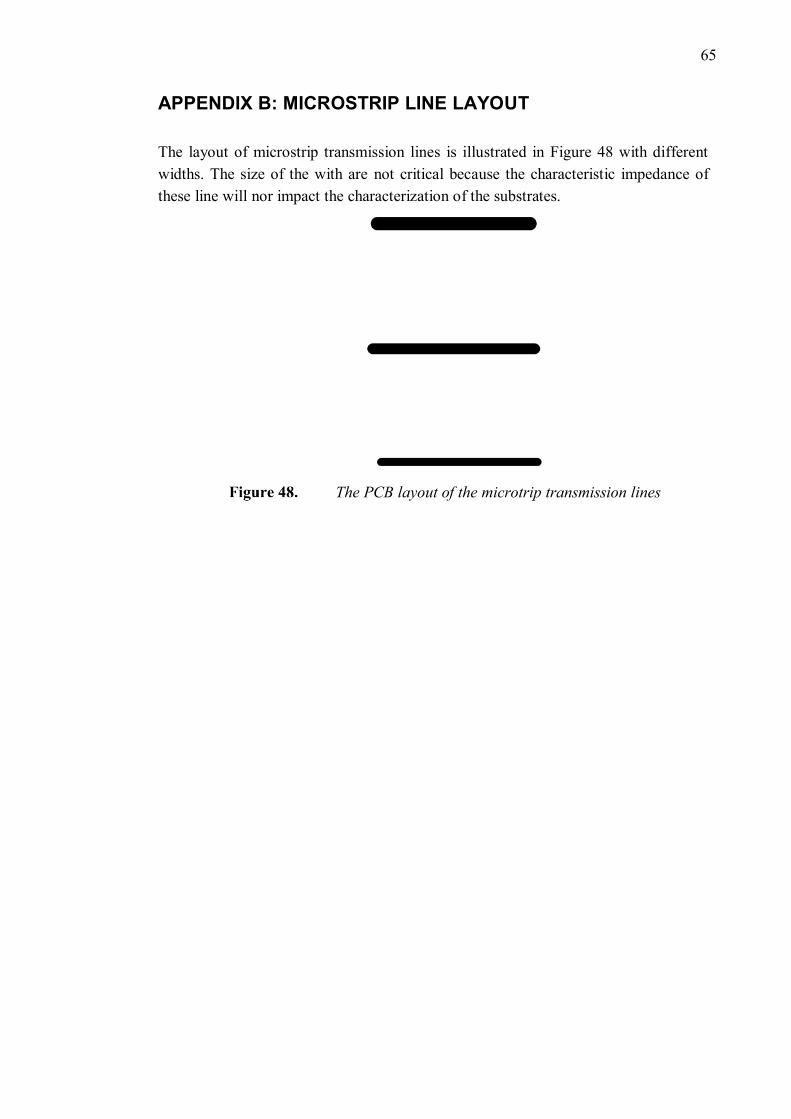
65 APPENDIX B: MICROSTRIP LINE LAYOUT The layout of microstrip transmission lines is illustrated in Figure 48 with different widths. The size of the with are not critical because the characteristic impedance of these line will nor impact the characterization of the substrates.
The PCB layout of the microtrip transmission lines