A unified IV model for PD/FD SOI MOSFETs with a compact model for floating body effects
Upload
independentCategory
view
4download
0
Solid-State Electronics 71 (2012) 19–24
Contents lists available at SciVerse ScienceDirect
Solid-State Electronics
journal homepage: www.elsevier .com/locate /sse
LaLuO3 higher-j dielectric integration in SOI MOSFETs with a gate-first process
A. Nichau a,⇑, E. Durgun Özben a, M. Schnee a, J.M.J. Lopes a,1, A. Besmehn b, M. Luysberg c, L. Knoll a,S. Habicht a, V. Mussmann a, R. Luptak a, St. Lenk a, J. Rubio-Zuazo d, G.R. Castro d, D. Buca a, Q.T. Zhao a,J. Schubert a, S. Mantl a
a Peter Grünberg Institute 9 (PGI-9-IT) and JARA-FIT, Forschungszentrum Jülich, 52425 Jülich, Germanyb Central Division for Chemical Analysis (ZCH), Forschungszentrum Jülich, 52425 Jülich, Germanyc Peter Grünberg Institute 5 and Ernst Ruska-Centre (ER-C) for Microscopy and Spectroscopy with Electrons, Forschungszentrum Jülich, 52425 Jülich, Germanyd Spanish CRG BM25 Beamline – SpLine, European Synchrotron Radiation Facility (ESRF), Rue Jules Horowitz BP 220, F-38043 Grenoble, Cedex 09, France
a r t i c l e i n f o
Article history:Available online 9 January 2012
Keywords:Lanthanum lutetium oxideGate-first
0038-1101/$ - see front matter � 2011 Elsevier Ltd. Adoi:10.1016/j.sse.2011.10.014
⇑ Corresponding author at: Peter Grünberg InstituForschungszentrum Jülich, 52425 Jülich, Germany.
E-mail address: [email protected] (A. Nichau)1 Present address: Paul-Drude-Institut für Festkör
Germany.
a b s t r a c t
The chemical reactions at the higher-j LaLuO3/Ti1NX/poly-Si gate stack interfaces are in detail investi-gated. Electrical and structural characterization methods are employed to explore the thermal stabilityof the gate stack. A Ti-rich TiN metal layer degrades the gate stack performance after high temperatureannealing while the gate stack with a near stoichiometric TiN layer is stable during 1000 �C, 5 s anneals.Based on these results an integration process of TiN/LaLuO3 in a gate-first MOSFET process on SOI isshown.
� 2011 Elsevier Ltd. All rights reserved.
1. Introduction
Lanthanum lutetium oxide (LaLuO3) has recently received a lot ofattention as being considered a promising higher-j dielectric [1,2].Its high relative permittivity of �32 in the amorphous state in con-junction with high thermal stability and low leakage current densi-ties enable its integration into future CMOS technology nodes [1,2]where an equivalent oxide thickness (EOT) below 0.9 nm is required.The implementation of higher-j oxides affords a thicker silicate/SiO2 interfacial layer (IL) when scaling down EOT [3]. An importantstep is the integration compatibility of higher-j dielectrics withchannel materials of increased mobility, like strained Si [4] andstrained Si(Ge) [5]. Recently, using a full replacement gate Dur-gun et al. showed excellent device characteristics using LaLuO3/TiN gate stack on strained Si channel [4] while Yu et al. presentedthe first integration into quantum well strained SiGe MOSFETsemploying a gate first process [7]. However, in both integration pro-cesses the gate stack annealing temperatures are below 650 �C.
In this contribution we present a detailed investigation on ther-mal treatments of TiNx/LaLuO3 stacks required for gate-first devicefabrication. Special emphasis is placed on the chemical layer stabil-ity as well as EOT and work function analysis. In the second part ofthe paper the integration of TiNx/LaLuO3 gate stacks in gate-firstfully depleted (FD) SOI devices is presented.
ll rights reserved.
te 9 (PGI-9-IT) and JARA-FIT,
.perelektronik, 10117 Berlin,
2. Experimental
For the gate stack analysis, the structure of interest consists of astack of thin high-j/metal layer on low doped p-Si (100) sub-strates formed by deposition of 10 nm LaLuO3 by molecular beamdeposition (MBD), and 15 nm TiNx by physical vapor deposition(PVD). Two different deposition conditions were chosen for TiNx
layers which results in Ti1N0.8 and Ti1N0.9 layers.The layer stoichiometry was determined by Rutherford back-
scattering spectrometry (RBS).To study the effect of doping activation on the gate stack the
samples were annealed in a rapid thermal processing (RTP) systemin nitrogen ambient for 5 s at 1000 �C or spike annealed at 1050 �C.
MOS capacitor structures used for electrical characterizationwere formed with 70 nm n+-poly-Si layers deposited at 580 �C bylow pressure chemical vapor deposition (LPCVD) on top of thehigh-j/metal layer stacks. Forming gas annealing (FGA) in 90%N2/10% H2 for 10 min at a temperature of 450 �C was carried outafter MOS (later also MOSFET) fabrication.
Scanning transmission electron microscopy (STEM) and electronenergy loss spectroscopy (EELS) investigations were performedwith a FEI Titan 300–80 on MOS capacitor after 1050 �C spike an-neals. The samples were prepared by focused ion beam (FIB).
The analysis of the chemical composition of the gate stack layersand interfaces after different annealing temperatures was per-formed employing hard X-ray photoemission spectra (HAXPES).The analyses were performed at the CRG SpLine at the EuropeanSynchrotron Radiation Facility (ESRF) Grenoble where the method-ology based of hard X-ray for studies of surfaces and interfaces has
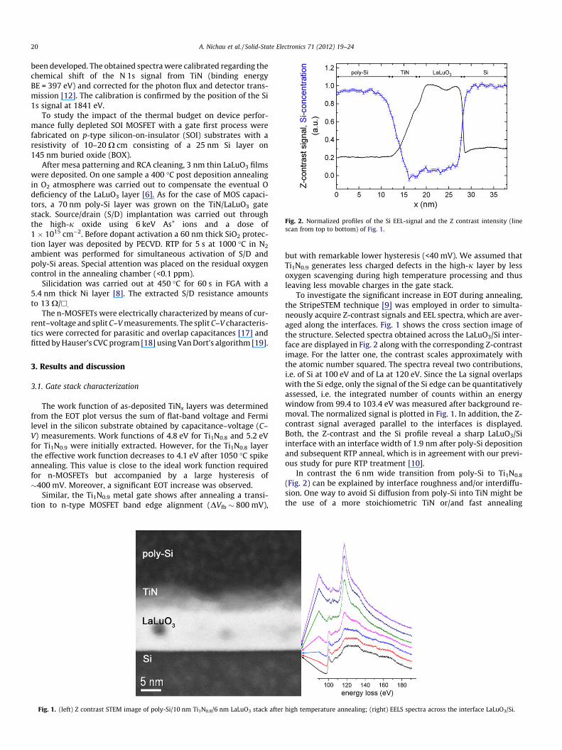
Fig. 2. Normalized profiles of the Si EEL-signal and the Z contrast intensity (linescan from top to bottom) of Fig. 1.
20 A. Nichau et al. / Solid-State Electronics 71 (2012) 19–24
been developed. The obtained spectra were calibrated regarding thechemical shift of the N 1s signal from TiN (binding energyBE = 397 eV) and corrected for the photon flux and detector trans-mission [12]. The calibration is confirmed by the position of the Si1s signal at 1841 eV.
To study the impact of the thermal budget on device perfor-mance fully depleted SOI MOSFET with a gate first process werefabricated on p-type silicon-on-insulator (SOI) substrates with aresistivity of 10–20 X cm consisting of a 25 nm Si layer on145 nm buried oxide (BOX).
After mesa patterning and RCA cleaning, 3 nm thin LaLuO3 filmswere deposited. On one sample a 400 �C post deposition annealingin O2 atmosphere was carried out to compensate the eventual Odeficiency of the LaLuO3 layer [6]. As for the case of MOS capaci-tors, a 70 nm poly-Si layer was grown on the TiN/LaLuO3 gatestack. Source/drain (S/D) implantation was carried out throughthe high-j oxide using 6 keV As+ ions and a dose of1 � 1015 cm�2. Before dopant activation a 60 nm thick SiO2 protec-tion layer was deposited by PECVD. RTP for 5 s at 1000 �C in N2
ambient was performed for simultaneous activation of S/D andpoly-Si areas. Special attention was placed on the residual oxygencontrol in the annealing chamber (<0.1 ppm).
Silicidation was carried out at 450 �C for 60 s in FGA with a5.4 nm thick Ni layer [8]. The extracted S/D resistance amountsto 13 X/h.
The n-MOSFETs were electrically characterized by means of cur-rent–voltage and split C–V measurements. The split C–V characteris-tics were corrected for parasitic and overlap capacitances [17] andfitted by Hauser’s CVC program [18] using Van Dort’s algorithm [19].
3. Results and discussion
3.1. Gate stack characterization
The work function of as-deposited TiNx layers was determinedfrom the EOT plot versus the sum of flat-band voltage and Fermilevel in the silicon substrate obtained by capacitance–voltage (C–V) measurements. Work functions of 4.8 eV for Ti1N0.8 and 5.2 eVfor Ti1N0.9 were initially extracted. However, for the Ti1N0.8 layerthe effective work function decreases to 4.1 eV after 1050 �C spikeannealing. This value is close to the ideal work function requiredfor n-MOSFETs but accompanied by a large hysteresis of�400 mV. Moreover, a significant EOT increase was observed.
Similar, the Ti1N0.9 metal gate shows after annealing a transi-tion to n-type MOSFET band edge alignment (DVfb � 800 mV),
Fig. 1. (left) Z contrast STEM image of poly-Si/10 nm Ti1N0.8/6 nm LaLuO3 stack after
but with remarkable lower hysteresis (<40 mV). We assumed thatTi1N0.9 generates less charged defects in the high-j layer by lessoxygen scavenging during high temperature processing and thusleaving less movable charges in the gate stack.
To investigate the significant increase in EOT during annealing,the StripeSTEM technique [9] was employed in order to simulta-neously acquire Z-contrast signals and EEL spectra, which are aver-aged along the interfaces. Fig. 1 shows the cross section image ofthe structure. Selected spectra obtained across the LaLuO3/Si inter-face are displayed in Fig. 2 along with the corresponding Z-contrastimage. For the latter one, the contrast scales approximately withthe atomic number squared. The spectra reveal two contributions,i.e. of Si at 100 eV and of La at 120 eV. Since the La signal overlapswith the Si edge, only the signal of the Si edge can be quantitativelyassessed, i.e. the integrated number of counts within an energywindow from 99.4 to 103.4 eV was measured after background re-moval. The normalized signal is plotted in Fig. 1. In addition, the Z-contrast signal averaged parallel to the interfaces is displayed.Both, the Z-contrast and the Si profile reveal a sharp LaLuO3/Siinterface with an interface width of 1.9 nm after poly-Si depositionand subsequent RTP anneal, which is in agreement with our previ-ous study for pure RTP treatment [10].
In contrast the 6 nm wide transition from poly-Si to Ti1N0.8
(Fig. 2) can be explained by interface roughness and/or interdiffu-sion. One way to avoid Si diffusion from poly-Si into TiN might bethe use of a more stoichiometric TiN or/and fast annealing
high temperature annealing; (right) EELS spectra across the interface LaLuO3/Si.
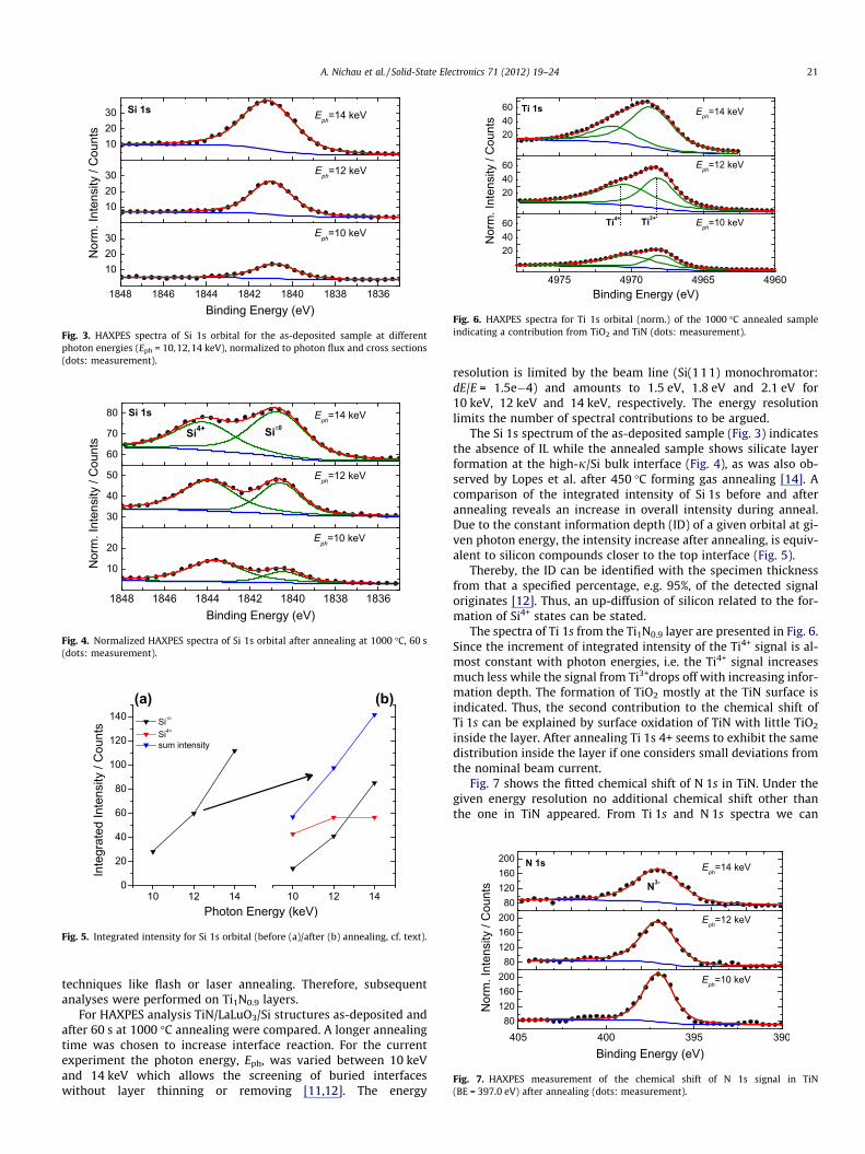
Fig. 3. HAXPES spectra of Si 1s orbital for the as-deposited sample at differentphoton energies (Eph = 10,12,14 keV), normalized to photon flux and cross sections(dots: measurement).
Fig. 6. HAXPES spectra for Ti 1s orbital (norm.) of the 1000 �C annealed sampleindicating a contribution from TiO2 and TiN (dots: measurement).
Fig. 7. HAXPES measurement of the chemical shift of N 1s signal in TiN(BE = 397.0 eV) after annealing (dots: measurement).
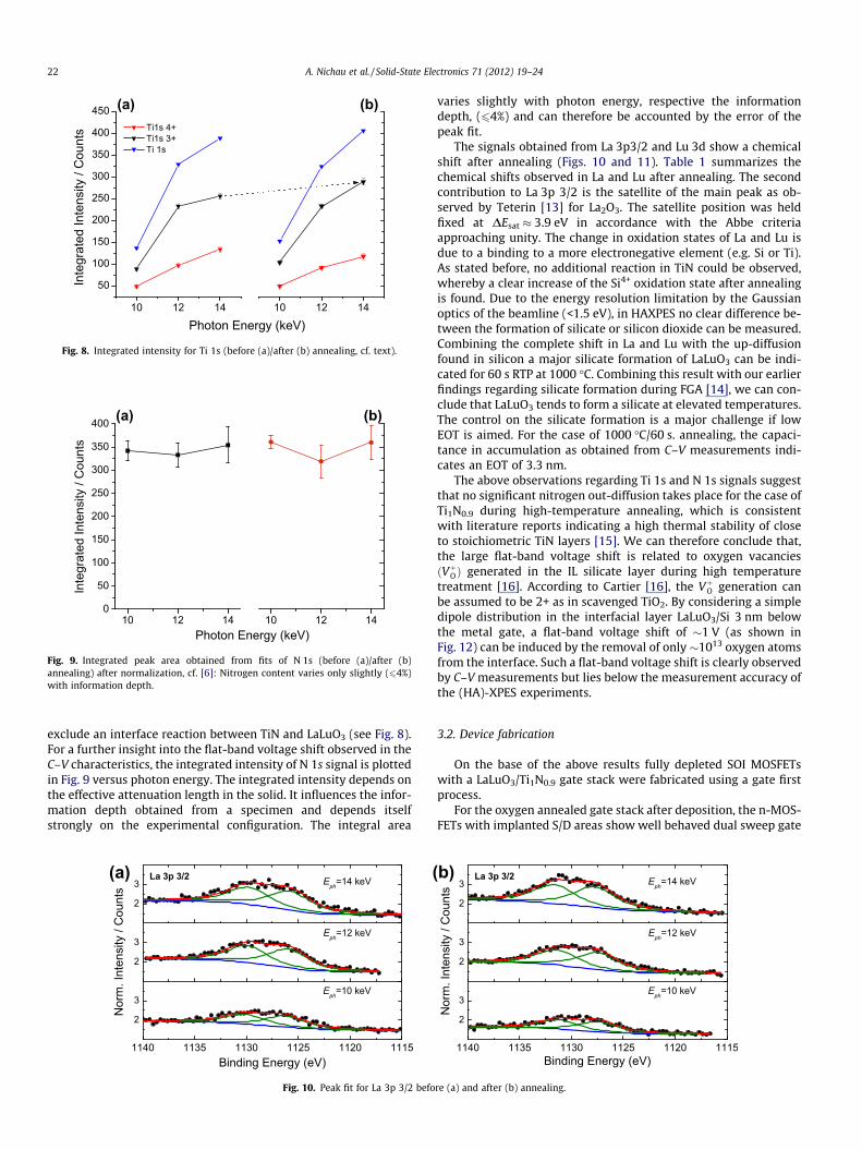
Fig. 4. Normalized HAXPES spectra of Si 1s orbital after annealing at 1000 �C, 60 s(dots: measurement).
(a) (b)
Fig. 5. Integrated intensity for Si 1s orbital (before (a)/after (b) annealing, cf. text).
A. Nichau et al. / Solid-State Electronics 71 (2012) 19–24 21
techniques like flash or laser annealing. Therefore, subsequentanalyses were performed on Ti1N0.9 layers.
For HAXPES analysis TiN/LaLuO3/Si structures as-deposited andafter 60 s at 1000 �C annealing were compared. A longer annealingtime was chosen to increase interface reaction. For the currentexperiment the photon energy, Eph, was varied between 10 keVand 14 keV which allows the screening of buried interfaceswithout layer thinning or removing [11,12]. The energy
resolution is limited by the beam line (Si(111) monochromator:dE/E = 1.5e�4) and amounts to 1.5 eV, 1.8 eV and 2.1 eV for10 keV, 12 keV and 14 keV, respectively. The energy resolutionlimits the number of spectral contributions to be argued.
The Si 1s spectrum of the as-deposited sample (Fig. 3) indicatesthe absence of IL while the annealed sample shows silicate layerformation at the high-j/Si bulk interface (Fig. 4), as was also ob-served by Lopes et al. after 450 �C forming gas annealing [14]. Acomparison of the integrated intensity of Si 1s before and afterannealing reveals an increase in overall intensity during anneal.Due to the constant information depth (ID) of a given orbital at gi-ven photon energy, the intensity increase after annealing, is equiv-alent to silicon compounds closer to the top interface (Fig. 5).
Thereby, the ID can be identified with the specimen thicknessfrom that a specified percentage, e.g. 95%, of the detected signaloriginates [12]. Thus, an up-diffusion of silicon related to the for-mation of Si4+ states can be stated.
The spectra of Ti 1s from the Ti1N0.9 layer are presented in Fig. 6.Since the increment of integrated intensity of the Ti4+ signal is al-most constant with photon energies, i.e. the Ti4+ signal increasesmuch less while the signal from Ti3+drops off with increasing infor-mation depth. The formation of TiO2 mostly at the TiN surface isindicated. Thus, the second contribution to the chemical shift ofTi 1s can be explained by surface oxidation of TiN with little TiO2
inside the layer. After annealing Ti 1s 4+ seems to exhibit the samedistribution inside the layer if one considers small deviations fromthe nominal beam current.
Fig. 7 shows the fitted chemical shift of N 1s in TiN. Under thegiven energy resolution no additional chemical shift other thanthe one in TiN appeared. From Ti 1s and N 1s spectra we can
(a) (b)
Fig. 8. Integrated intensity for Ti 1s (before (a)/after (b) annealing, cf. text).
(a) (b)
Fig. 9. Integrated peak area obtained from fits of N 1s (before (a)/after (b)annealing) after normalization, cf. [6]: Nitrogen content varies only slightly (64%)with information depth.
22 A. Nichau et al. / Solid-State Electronics 71 (2012) 19–24
exclude an interface reaction between TiN and LaLuO3 (see Fig. 8).For a further insight into the flat-band voltage shift observed in theC–V characteristics, the integrated intensity of N 1s signal is plottedin Fig. 9 versus photon energy. The integrated intensity depends onthe effective attenuation length in the solid. It influences the infor-mation depth obtained from a specimen and depends itselfstrongly on the experimental configuration. The integral area
(a) (
Fig. 10. Peak fit for La 3p 3/2 befo
varies slightly with photon energy, respective the informationdepth, (64%) and can therefore be accounted by the error of thepeak fit.
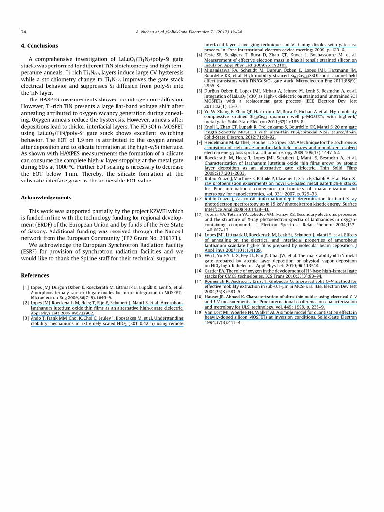
The signals obtained from La 3p3/2 and Lu 3d show a chemicalshift after annealing (Figs. 10 and 11). Table 1 summarizes thechemical shifts observed in La and Lu after annealing. The secondcontribution to La 3p 3/2 is the satellite of the main peak as ob-served by Teterin [13] for La2O3. The satellite position was heldfixed at DEsat � 3.9 eV in accordance with the Abbe criteriaapproaching unity. The change in oxidation states of La and Lu isdue to a binding to a more electronegative element (e.g. Si or Ti).As stated before, no additional reaction in TiN could be observed,whereby a clear increase of the Si4+ oxidation state after annealingis found. Due to the energy resolution limitation by the Gaussianoptics of the beamline (<1.5 eV), in HAXPES no clear difference be-tween the formation of silicate or silicon dioxide can be measured.Combining the complete shift in La and Lu with the up-diffusionfound in silicon a major silicate formation of LaLuO3 can be indi-cated for 60 s RTP at 1000 �C. Combining this result with our earlierfindings regarding silicate formation during FGA [14], we can con-clude that LaLuO3 tends to form a silicate at elevated temperatures.The control on the silicate formation is a major challenge if lowEOT is aimed. For the case of 1000 �C/60 s. annealing, the capaci-tance in accumulation as obtained from C–V measurements indi-cates an EOT of 3.3 nm.
The above observations regarding Ti 1s and N 1s signals suggestthat no significant nitrogen out-diffusion takes place for the case ofTi1N0.9 during high-temperature annealing, which is consistentwith literature reports indicating a high thermal stability of closeto stoichiometric TiN layers [15]. We can therefore conclude that,the large flat-band voltage shift is related to oxygen vacanciesðVþOÞ generated in the IL silicate layer during high temperaturetreatment [16]. According to Cartier [16], the VþO generation canbe assumed to be 2+ as in scavenged TiO2. By considering a simpledipole distribution in the interfacial layer LaLuO3/Si 3 nm belowthe metal gate, a flat-band voltage shift of �1 V (as shown inFig. 12) can be induced by the removal of only �1013 oxygen atomsfrom the interface. Such a flat-band voltage shift is clearly observedby C–V measurements but lies below the measurement accuracy ofthe (HA)-XPES experiments.
3.2. Device fabrication
On the base of the above results fully depleted SOI MOSFETswith a LaLuO3/Ti1N0.9 gate stack were fabricated using a gate firstprocess.
For the oxygen annealed gate stack after deposition, the n-MOS-FETs with implanted S/D areas show well behaved dual sweep gate
b)
re (a) and after (b) annealing.

(a) (b)
Fig. 11. Peak fit for Lu 3d 5/2 before (a) and after (b) annealing.
Table 1Chemical shift observed for La and Lu after 60 s at 1000 �C/anneal.
10 keV 12 keV 14 keV
DELu3d +1.4 eV +1.3 eV +1.5 eVDELa3p3/2 +1.1 eV +1.5 eV +1.9 eV
Fig. 12. Dual sweep split C–V characteristic for TiN/LaLuO3/SOI gate stack.
Fig. 13. Transfer characteristics of a FD SOI n-MOSFET with TiN/LaLuO3 gate stack.
Fig. 14. Output characteristics of FD SOI n-MOSFET with TiN/LaLuO3 gate stack andNiSi S/D contacts (lg = 2 lm, Vg–Vt = 0.5. . .1.5 V).
Fig. 15. TEM of readily processed MOSFET with 3 nm LaLuO3 gate oxide.
A. Nichau et al. / Solid-State Electronics 71 (2012) 19–24 23
capacitance curves (Fig. 12) with negligible hysteresis (<40 mV).The effective work function of 4.19 eV is shifted only by �0.14 eVfrom the Si n-MOSFET band edge. The EOT of 1.9 nm is fairly largecompared to our previous results obtained with a replacement gateprocess for HfO2 or LaLuO3 gate stacks [4]. Equally processed HfO2
reference samples (not shown) showed an EOT of 1.4 nm for a2.5 nm thin HfO2 layer on chemical oxide. However, those samplesdid not see additional oxygen anneal (400 �C, 10 min). The transfercharacteristics of a FD SOI n-MOSFET with a 3 nm LaLuO3 gatedielectric and 15 nm Ti1N0.9 are presented in Fig. 13. Gate-in-duced-drain-leakage (GIDL) is observed below �0.35 V. Good sub-threshold slopes of 60–70 mV/dec were extracted for all devices.
The devices with NiSi S/D contacts show high on-current up to75 lA/lm for gate length of 2 lm compared to the devices withdoped Al contacts (Fig. 14). The integration of LaLuO3 with TiN asmetal gate and NiSi S/D area results into good performance on longchannel devices. After scaling EOT short-channel transistors withLaLuO3/TiN gate stacks seem promising (see Fig. 15).
24 A. Nichau et al. / Solid-State Electronics 71 (2012) 19–24
4. Conclusions
A comprehensive investigation of LaLuO3/Ti1NX/poly-Si gatestacks was performed for different TiN stoichiometry and high tem-perature anneals. Ti-rich Ti1N0.8 layers induce large CV hysteresiswhile a stoichiometry change to Ti1N0.9 improves the gate stackelectrical behavior and suppresses Si diffusion from poly-Si intothe TiN layer.
The HAXPES measurements showed no nitrogen out-diffusion.However, Ti-rich TiN presents a large flat-band voltage shift afterannealing attributed to oxygen vacancy generation during anneal-ing. Oxygen anneals reduce the hysteresis. However, anneals afterdepositions lead to thicker interfacial layers. The FD SOI n-MOSFETusing LaLuO3/TiN/poly-Si gate stack shows excellent switchingbehavior. The EOT of 1.9 nm is attributed to the oxygen annealafter deposition and to silicate formation at the high-j/Si interface.As shown with HAXPES measurements the formation of a silicatecan consume the complete high-j layer stopping at the metal gateduring 60 s at 1000 �C. Further EOT scaling is necessary to decreasethe EOT below 1 nm. Thereby, the silicate formation at thesubstrate interface governs the achievable EOT value.
Acknowledgements
This work was supported partially by the project KZWEI whichis funded in line with the technology funding for regional develop-ment (ERDF) of the European Union and by funds of the Free Stateof Saxony. Additional funding was received through the Nanosilnetwork from the European Community (FP7 Grant No. 216171).
We acknowledge the European Synchrotron Radiation Facility(ESRF) for provision of synchrotron radiation facilities and wewould like to thank the SpLine staff for their technical support.
References
[1] Lopes JMJ, Durgun Özben E, Roeckerath M, Littmark U, Lupták R, Lenk S, et al.Amorphous ternary rare-earth gate oxides for future integration in MOSFETs.Microelectron Eng 2009;86(7–9):1646–9.
[2] Lopes JMJ, Roeckerath M, Heeg T, Rije E, Schubert J, Mantl S, et al. Amorphouslanthanum lutetium oxide thin films as an alternative high-j gate dielectric.Appl Phys Lett 2006;89:222902.
[3] Ando T, Frank MM, Choi K, Choi C, Bruley J, Hopstaken M, et al. Understandingmobility mechanisms in extremely scaled HfO2 (EOT 0.42 m) using remote
interfacial layer scavenging technique and Vt-tuning dipoles with gate-firstprocess. In: Proc international electron device meeting; 2009. p. 423–6.
[4] Feste SF, Schäpers T, Buca D, Zhao QT, Knoch J, Bouhassoune M, et al.Measurement of effective electron mass in biaxial tensile strained silicon oninsulator. Appl Phys Lett 2009;95:182101.
[5] Minamisawa RA, Schmidt M, Durgun Özben E, Lopes JMJ, Hartmann JM,Bourdelle KK, et al. High mobility strained Si0.5Ge0.5/SSOI short channel fieldeffect transistors with TiN/GdScO3 gate stack. Microelectron Eng 2011;88(9):2955–8.
[6] Durgun Özben E, Lopes JMJ, Nichau A, Schnee M, Lenk S, Besmehn A, et al.Integration of LaLuO3 (j30) as High-j dielectric on strained and unstrained SOIMOSFETs with a replacement gate process. IEEE Electron Dev Lett2011;32(1):15–7.
[7] Yu W, Zhang B, Zhao QT, Hartmann JM, Buca D, Nichau A, et al. High mobilitycompressive strained Si0.5Ge0.5 quantum well p-MOSFETs with higher-k/metal-gate. Solid-State Electron 2011;62(1):185–8.
[8] Knoll L, Zhao QT, Luptak R, Trellenkamp S, Bourdelle KK, Mantl S. 20 nm gatelength Schottky MOSFETs with ultra-thin NiSi/epitaxial NiSi2 source/drain.Solid-State Electron, 2012;71:88-92.
[9] Heidelmann M, Barthel J, Houben L. StripeSTEM. A technique for the isochronousacquisition of high angle annular dark-field images and monolayer resolvedelectron energy loss spectra. Ultramicroscopy 2009;109(12):1447–52.
[10] Roeckerath M, Heeg T, Lopes JMJ, Schubert J, Mantl S, Besmehn A, et al.Characterization of lanthanum lutetium oxide thin films grown by atomiclayer deposition as an alternative gate dielectric. Thin Solid Films2008;517:201–2033.
[11] Rubio-Zuazo J, Martínez E, Batude P, Clavelier L, Soria F, Chabli A, et al. Hard X-ray photoemission experiments on novel Ge-based metal gate/high-k stacks.In: Proc international conference on frontiers of characterization andmetrology for nanoelectronics, vol. 931; 2007. p. 329–33.
[12] Rubio-Zuazo J, Castro GR. Information depth determination for hard X-rayphotoelectron spectroscopy up to 15 keV photoelectron kinetic energy. SurfaceInterface Anal 2008;40:1438–43.
[13] Teterin YA, Teterin YA, Lebedev AM, Ivanov KE. Secondary electronic processesand the structure of X-ray photoelectron spectra of lanthanides in oxygen-containing compounds. J Electron Spectrosc Relat Phenom 2004;137–140:607–12.
[14] Lopes JMJ, Littmark U, Roeckerath M, Lenk St, Schubert J, Mantl S, et al. Effectsof annealing on the electrical and interfacial properties of amorphouslanthanum scandate high-k films prepared by molecular beam deposition. JAppl Phys 2007;101:104109.
[15] Wu L, Yu HY, Li X, Pey KL, Pan JS, Chai JW, et al. Thermal stability of TiN metalgate prepared by atomic layer deposition or physical vapor depositionon HfO2 high-K dielectric. Appl Phys Lett 2010;96:113510.
[16] Cartier EA. The role of oxygen in the development of Hf-base high-k/metal gatestacks for CMOS technologies. ECS Trans 2010;33(3):83–94.
[17] Romanjek K, Andrieu F, Ernst T, Ghibaudo G. Improved split C–V method foreffective mobility extraction in sub-0.1-lm Si MOSFETs. IEEE Electron Dev Lett2004;25(8):583–5.
[18] Hauser JR, Ahmed K. Characterization of ultra-thin oxides using electrical C–Vand I–V measurements. In: Proc international conference on characterizationand metrology for ULSI technology, vol. 449; 1998. p. 235–9.
[19] Van Dort MJ, Woerlee PH, Walker AJ. A simple model for quantisation effects inheavily-doped silicon MOSFETs at inversion conditions. Solid-State Electron1994;37(3):411–4.
Copyright © 2022 FDOKUMEN