
Lab 1: Introduction to MipsIt
87
Computer Structure Laboratory MipsIt Introduction Page 1 Lab 1: Introduction to MipsIt (Updated at 21/01/2019) Work at home (planned) time: 1:30 h Lab time: 2:30 h 1. Introduction In this first laboratory session we will study the simulation and assembly programs for the MIPS microprocessor (MipSit), which comprises programming software and a CPU simulator. The simulator enables programs written in assembler or C language to be compiled and simulated. The simulation environment has a memory hierarchy that can be fully configured by the user as well as an input/output system with interrupts and a visualization console. This platform will be used for the first five sessions of Computer Structure Laboratory. We first describe the components of the programming environment and the procedures to be followed. We then use several examples to show the compilation and simulation methodologies. This strategy will enable us to review and consolidate several concepts seen on previous courses and to review the relationship between the programming language and the computer hardware we are going to study on this course. These laboratory sessions will reinforce the knowledge students have acquired in their theoretical classes. Students will also continue to develop basic techniques for collecting data and representing those data in table or graph format. Before each laboratory session, all members of each working group are required to read the documentation on the theoretical foundation for the work they will perform and the tools they will use. Preliminary reading of these documents will help them to use the software and laboratory equipment and answer questions on their use and functionality. In each laboratory session students should create a teamwork methodology that enables them to take maximum profit from the session. You need to be on time and pay attention to the lecturer’s instructions. This is important especially for this first session where we will present the ground rules to ensure that all sessions are conducted properly. Goals On completion of this session you will be able to - understand the basic components and capabilities of MipsIt, - configure the MipsIt simulator, - create a project with MipsIt (Assembler and C (minimal)/Assembler), - compile/link and simulate a program with MipsIt, and - understand the interaction between high-level programs and microprocessor components, i.e. data storage, variable alignment, and the read/write operations of I/O devices. Lab 1
-
Upload
khangminh22 -
Category
Documents
-
view
4 -
download
0
Transcript of Lab 1: Introduction to MipsIt
Computer Structure Laboratory
MipsIt Introduction Page 1
Lab1:IntroductiontoMipsIt
(Updated at 21/01/2019) Work at home (planned) time: 1:30 h
Lab time: 2:30 h
1. Introduction
In this first laboratory session we will study the simulation and assembly programs for the MIPS microprocessor (MipSit), which comprises programming software and a CPU simulator. The simulator enables programs written in assembler or C language to be compiled and simulated. The simulation environment has a memory hierarchy that can be fully configured by the user as well as an input/output system with interrupts and a visualization console. This platform will be used for the first five sessions of Computer Structure Laboratory.
We first describe the components of the programming environment and the procedures to be followed. We then use several examples to show the compilation and simulation methodologies. This strategy will enable us to review and consolidate several concepts seen on previous courses and to review the relationship between the programming language and the computer hardware we are going to study on this course.
These laboratory sessions will reinforce the knowledge students have acquired in their theoretical classes. Students will also continue to develop basic techniques for collecting data and representing those data in table or graph format. Before each laboratory session, all members of each working group are required to read the documentation on the theoretical foundation for the work they will perform and the tools they will use. Preliminary reading of these documents will help them to use the software and laboratory equipment and answer questions on their use and functionality.
In each laboratory session students should create a teamwork methodology that enables them to take maximum profit from the session. You need to be on time and pay attention to the lecturer’s instructions. This is important especially for this first session where we will present the ground rules to ensure that all sessions are conducted properly.
Goals
On completion of this session you will be able to
- understand the basic components and capabilities of MipsIt,
- configure the MipsIt simulator,
- create a project with MipsIt (Assembler and C (minimal)/Assembler),
- compile/link and simulate a program with MipsIt, and
- understand the interaction between high-level programs and microprocessor components, i.e.data storage, variable alignment, and the read/write operations of I/O devices.
Lab 1
Computer Structure Laboratory
MipsIt Introduction Page 2
Resources
For these laboratory classes a personal computer will be available with the Windows operating system and the MipsIt simulator. The MIPS simulator can be downloaded for Windows from the Aula Virtual. The file must be unzipped and stored in any directory under any name without spaces. The bin directory contains the executable programs. In these laboratory sessions you will use two of these, i.e.:
MipsIt.exe: MipsIt Studio 2000 (MIPS programming environment).
Mips.exe: MipsSim (MIPS simulator).
You will find further information about this platform in Annex I.
Learning process and evaluation
Pre-Lab work. Some work must be completed before each session. Typically, you should read the documents for that session and answer the questions indicated as preliminary work. This preliminary work will be evaluated during a brief interview with your lecturer at the beginning of the session. Students who are not yet members of a workgroup should complete this work individually. Later, during the laboratory class, they will be sorted into groups.
In-Lab work. This component is evaluated in accordance with the work conducted in the lab. This work will be conducted in several stages with a range of activities weighted according to their complexity. On completion of each activity, students should call their lecturer to check that they have understood the task and completed it successfully. The lecturer can ask any task-related question to check whether the students has fully understood the problem and completed it in an original way. At the end of each laboratory session, students must also write up their answers to the questions posed during the session and hand these in to their lecturer.
Post-Lab work. For some laboratory sessions, students may also be required to prepare a short report. These reports may involve presenting tables or graphs of the measurements they have taken in the laboratory, providing justifications or theoretical explanations for those measurements, extending or generalizing some of the work they have completed, or completing several tasks in relation to the work they have carried out during the session. This report must be submitted before or at the beginning of the next laboratory session.
Student evaluation for each session will comprise the sum of the evaluations of their pre-lab work, laboratory work (typically between 2 and 3), and post-lab work (if applicable). Each component is evaluated with an A (Good), B (Regular) or C (Bad). The numerical value assigned to each letter depends on the number of stages. However, all A’s awarded to students who have completed all the tasks well will be equivalent to a score of 9. A score of 10 is reserved for groups that have been awarded all A’s for their laboratory session or have provided solutions of exceptional value and originality.

Computer Structure Laboratory
MipsIt Introduction Page 3
2. Preliminary (pre-lab) work
To make the most of your laboratory sessions you must complete all the following activities, spending the suggested amount of time on them. So as not to exceed the estimated maximum length of time suggested for each activity, all workgroup members must share the workload appropriately. If activities are not shared out appropriately or if any member tries to do too much work, the time available for other activities may be affected.
For their Pre-Lab work, all team members should read Annex I of this document, which describes the components of the MipsIt environment and explains how to work with it. It is important that you do this because it is your first contact with the software you will be working with in the next five laboratory sessions. You should also check certain ideas about the computer memory that you have studied so far. For some final questions, you will need to check some of the bibliographic sources shown or that are available on the Internet.
After reading Annex I, answer the following questions (these answers must be handed in at the beginning of the session):
Q1. Briefly describe the elements that make up the computer implemented in the simulator.
Q2. How many lines form the address bus of this microprocessor and how much memory can be addressed?
Q3. Indicate the positions of the computer’s main memory and explain which RAM technologies have been used in its implementation. Explain the differences between these two technologies.
Q4. What kind of architecture (Von Neumann or Harvard) does the computer implement in the cache memory simulator?
Q5. Explain which memory positions occupy all the Input/Output ports of the simulated computer.
Q6. What is the size of the data we can read or write in the Input/Output ports?
Q7. What are the positions from which an integer must be stored so that it is properly aligned in the simulator memory?
Q8. What kind of data will always be aligned in C?
First checkpoint: Answers to Q1-Q8 must be written up and handed to the lecturer at the beginning of the session.
Computer Structure Laboratory
MipsIt Introduction Page 4
3. Lab (in-lab) work
In this session we will use MipsIt and check its functioning in a practical way with various programs that access its components. Answers to the questions must be written up and handed in at the end of the session.
3.1 To introduce students to the compiler and simulator, the C program below must be compiled and executed. To do so, the program (MipsIt.exe) must be executed. This program can be found in C:\Mipsit\bin. Just after the program begins, it may signal an error message related to ports that are not open, but the program will be executed normally. Initially, a project must be created (Project menu) with the option C(minimal)/Assembler. Files must not be saved in directories that contain spaces, accent marks or long names, so we recommended that you work in C:\tmp. Once there, you need to create a subdirectory with a suitable name, e.g. P1-1 (practice 1, part 1). In addition, a new C file associated with the project must be created with a “.c” extension. This should have the same name as the project: in this case, P1-1.c. The program code reads the value of the inputs and the position of I/O (input/output) 0xbf900000, and writes the read value on the same address, which shows this value in the LED bar.
#define TRUE 1 unsigned char *Switches = (char*) 0xbf900000; unsigned char *leds = (char*) 0xbf900000; int main () { while (TRUE) { *leds=*Switches; printf("The input value is: %X \n",*Switches); } }
- The default compiler options must be edited whenever you wish to access the Input/Output space. These options remain linked to each project and are saved with it but, since they are not retained for the next project, they must be checked each time a new non-saved project is compiled. It is a good idea is to have a txt file open with the Notepad, from which you can copy the 2 boxes that must be edited (these appear in red below). The options to edit are in Project> Settings in the Link tab:
Base address: 0x80020000 Entry-point symbol: start Libraries: kil,c,m,lnk,gcc,soft-float Modules: crt0.o Linker options: -Ttext 0x80020000 -e start -lkil -lc -lm -llnk -lgcc -lsoft-float -N -nostdlib
- The project must be built in the compilation environment (F7). It should work, and the following messages should appear: Linking ... Post Build ... Done.
- Now the simulator should be opened (c:\Mipsit\bin\Mips.exe) and the code must be loaded into the simulator using the option Build>Upload>To Simulator (or F5). Once the code is loaded in the simulator, the name will appear in the upper part of the window P1-1.out.
Computer Structure Laboratory
MipsIt Introduction Page 5
- The program must be executed with the Cpu>Run simulator option or by pressing the button with the play symbol. A console will appear showing the printf message. To check the code works properly, the output input module must be opened with View>I/O. Now change the inputs associated with the input port through the switches. The LEDs must be activated with the pressed values. You must also check that the output value we have in the console matches the value entered by the switches.
Q9. Why is the port pointer an unsigned char type?
3.2 In this new program, two integer data (32 bits) are accessed in memory locations 0x80020000 and 0xA0020000. A new project must be created (P1-2) with the explained methodology and with a new C code (P1-2.c). The program code will be:
#define TRUE 1 int *pos1 = (int*) 0x80020000; int *pos2 = (int*) 0xA0020000; int main () { *pos2=0x00000000; *pos1=0xf0f0f0f0; printf("The memory 1 value is: %X \n",*pos1); printf("The memory 2 value is: %X \n",*pos2); while (TRUE); }
- You need to build the project in the compilation environment and simulate it.
Q10. Check the assembly code generated in the two previous examples and look when the CPU is accessing the I/O or the memory positions. What instruction is used to access the I/O positions? What instruction is used to access the memory positions in the MIPS? Is there any difference between these two types of access?
Q11. How many bytes does an instruction have? How many memory positions does it occupy? In which kind of position does an instruction begin? Which kind of byte order (Little-endian or Big-endian) is used?
3.3 In this case, two integer variables are accessed in the memory positions 0x80020000 and 0x80020001. The program code is:
#define TRUE 1 int *pos1 = (int*) 0x80020001; int *pos2 = (int*) 0x80020000; int main () { *pos2=0x00000000; *pos1=0xf0f0f0f0; printf("The memory 1 value is: %X \n",*pos1); printf("The memory 2 value is: %X \n",*pos2); while (TRUE); }
-You must build the project in the compilation software and simulate it.
- Does the program work properly? What problem do you think it has?
Computer Structure Laboratory
MipsIt Introduction Page 6
Second checkpoint: Call the lecturer and answer the questions in sections 3.2 and 3.3 or any other question related to these sections.
3.4 In this case, the entry position of the interrupts is accessed and its value is displayed.
#define TRUE 1 unsigned char *interrupt = (char*) 0xbfa00000; int main () { while (TRUE){ printf("The entry value is: %X \n",*interrupt); } }
The project must be built in the compilation software and be simulated.
The interrupt switches K1 and K2 must be pressed alternately. Then check and write down the values obtained by the entry position of the interrupts in each case. Discuss the results obtained by pressing the same switch several times.
3.5 You must implement a program in C code that read the inputs of the I/O module located in position 0xbf900000 associated with the switches. Accordingly, this value must turn ON the output LEDs as a level bar. The ranges of the input values with their corresponding output values are:
Input Output
0 - 31 1 (activates only 1st led)
32 - 63 2 (activates only 2nd led)
64 - 95 4 (activates only 3rd led)
96 -127 8 (activates only 4th led)
128 - 159 16 (activates only 5th led)
160 - 191 32 (activates only 6th led)
192 - 223 64 (activates only 7th led)
224 - 255 128 (activates only 8th led)
Implement the program and simulate its correct functioning. Once you have finished, you must show the code to your lecturer.
Third checkpoint: Call the lecturer and answer the questions in sections 3.4 and 3.5 or any other question related to these sections.
The answers to Q1-Q11 must be written up and handed in to your lecturer.
Computer Structure Laboratory
MipsIt Introduction Page 7
AnnexI:MipsItStudio2000Introduction
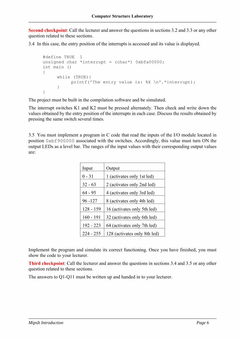
MipsIt is the software in which the programs for the first five practice sessions are written. The project is the basic concept for working in MipsIt Studio 2000. In this case this concept, already seen on previous programming and hardware design courses, can be understood as a set of interrelated source files that are compiled and linked to generate an executable file to be sent to the MIPS processor simulator. A MipsIt project can contain programs written in MIPS assembler, programs written in C language, and text files. In the programming interface we can see the following windows:
The Program window shows the contents of the files.
The Workspace window contains a list of all the files included in the project.
The Output window provides information during the compilation and assembly phases.
MipsIt windows
Configuration
In the File menu, Options sub-menu, you can configure MipsIt Studio 2000. Specifically, you can specify the directories in which to place the executable files (bin), the library files (lib) and the header files (include) for the application. You can also specify the location of the compiler (bin/xgcc.exe).
How to create a new project
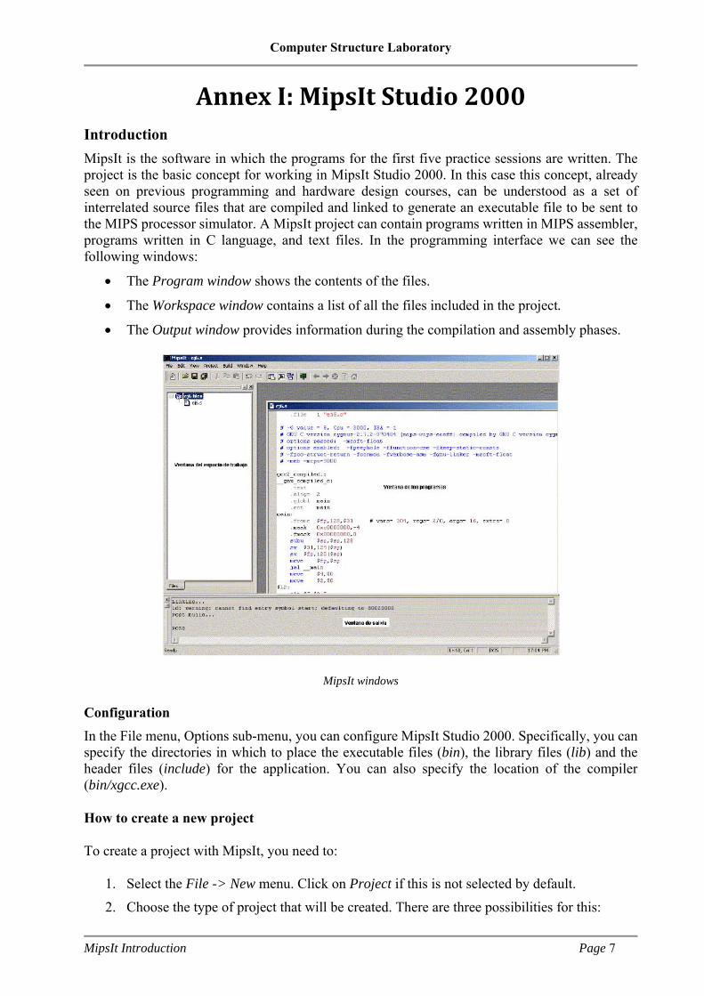
To create a project with MipsIt, you need to:
1. Select the File -> New menu. Click on Project if this is not selected by default.
2. Choose the type of project that will be created. There are three possibilities for this:
Computer Structure Laboratory
MipsIt Introduction Page 8
a. Assembler: The project contains files only in assembler.
b. C/Assembler: The project contains files only in C language or C files and assembly code. Programs with this option cannot be simulated with MipsSim.
c. C(minimal)/Assembler: This is the same as in the previous case but only basic files of essential libraries are used. Programs with this option can be simulated with MipsSim.
3. The name of the project must be entered in Project Name and its location must be specified in Location.
4. Finally, click Aceptar in the window that appears below.
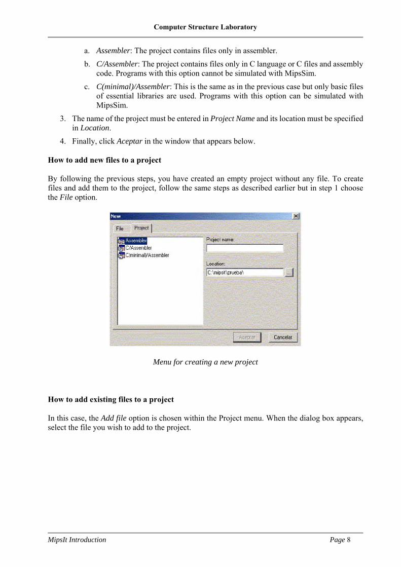
How to add new files to a project
By following the previous steps, you have created an empty project without any file. To create files and add them to the project, follow the same steps as described earlier but in step 1 choose the File option.
Menu for creating a new project
How to add existing files to a project
In this case, the Add file option is chosen within the Project menu. When the dialog box appears, select the file you wish to add to the project.
Computer Structure Laboratory
MipsIt Introduction Page 9
Menu for adding a new file to a project
Compilation and assembly
If the Build>Build menu is chosen, all the files in C language will be compiled and all the project files will be assembled and linked. In the output window, information messages will appear about how the process has developed and whether there are any errors, etc. If you wish to recompile the whole project, you must choose the option Rebuild All from the Build menu.
Assembly code generated by C programs
If any programs are written in C language, you can see the equivalent assembly program generated by MipsIt. To do so, once the program is compiled, the file written in C must be opened and the menu option Build->View Assembler must be selected.
MipsSim: MIPS simulator (Mips.exe)
Introduction
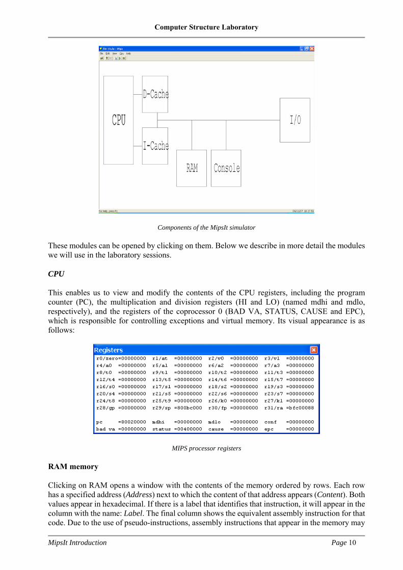
If a board with the MIPS processor is not available, a MIPS simulator is needed to check the functioning of the written programs. The MipsSim is a graphical environment that enables us to see the status of the memory, the CPU registers, the output console, etc., at any time during the execution of the program. Double-clicking on the Mips.exe file icon opens the following window with the modules:
CPU: MIPS R2000 microprocessor.
RAM Memory: Main memory.
Console: Standard I/O.
I/O: I/O 8-bit port.
D-Cache and I-Cache: Data and instructions separated cache memories.
Computer Structure Laboratory
MipsIt Introduction Page 10
Components of the MipsIt simulator
These modules can be opened by clicking on them. Below we describe in more detail the modules we will use in the laboratory sessions.
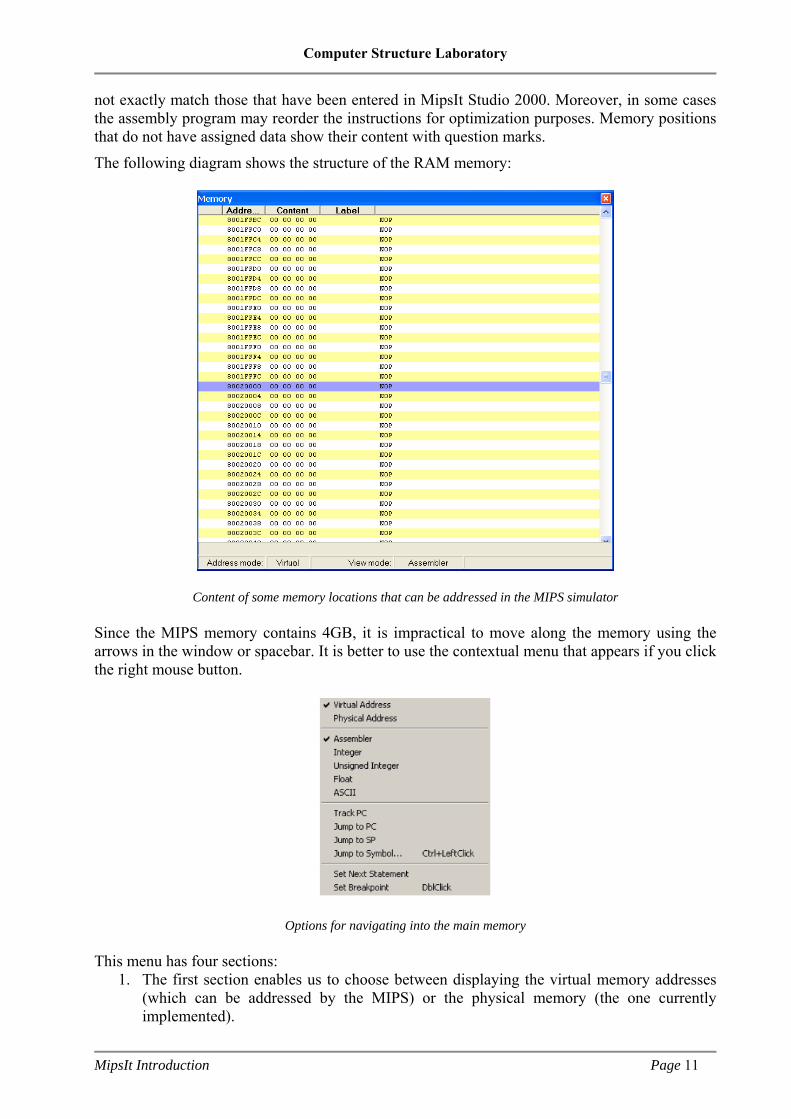
CPU
This enables us to view and modify the contents of the CPU registers, including the program counter (PC), the multiplication and division registers (HI and LO) (named mdhi and mdlo, respectively), and the registers of the coprocessor 0 (BAD VA, STATUS, CAUSE and EPC), which is responsible for controlling exceptions and virtual memory. Its visual appearance is as follows:
MIPS processor registers
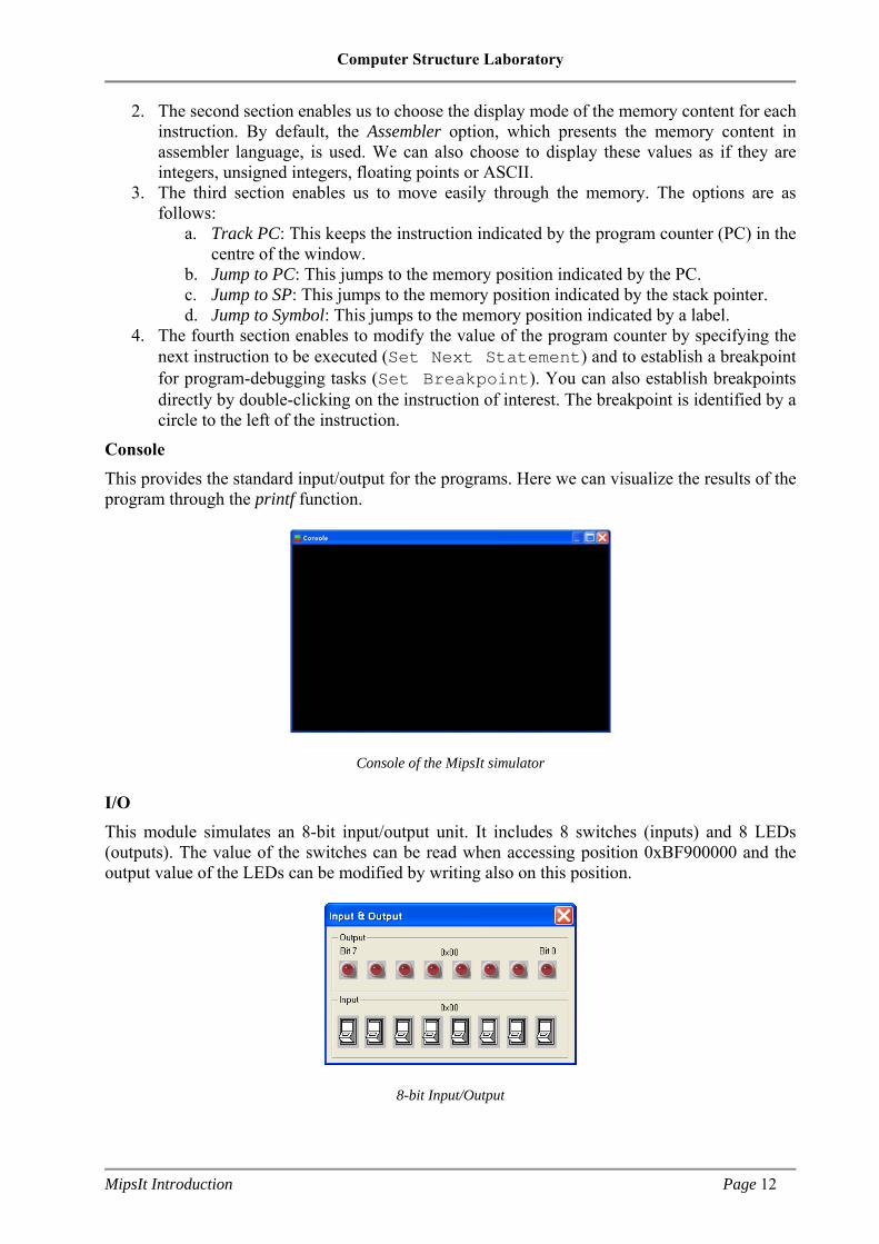
RAM memory
Clicking on RAM opens a window with the contents of the memory ordered by rows. Each row has a specified address (Address) next to which the content of that address appears (Content). Both values appear in hexadecimal. If there is a label that identifies that instruction, it will appear in the column with the name: Label. The final column shows the equivalent assembly instruction for that code. Due to the use of pseudo-instructions, assembly instructions that appear in the memory may
Computer Structure Laboratory
MipsIt Introduction Page 11
not exactly match those that have been entered in MipsIt Studio 2000. Moreover, in some cases the assembly program may reorder the instructions for optimization purposes. Memory positions that do not have assigned data show their content with question marks.
The following diagram shows the structure of the RAM memory:
Content of some memory locations that can be addressed in the MIPS simulator
Since the MIPS memory contains 4GB, it is impractical to move along the memory using the arrows in the window or spacebar. It is better to use the contextual menu that appears if you click the right mouse button.
Options for navigating into the main memory
This menu has four sections: 1. The first section enables us to choose between displaying the virtual memory addresses
(which can be addressed by the MIPS) or the physical memory (the one currently implemented).
Computer Structure Laboratory
MipsIt Introduction Page 12
2. The second section enables us to choose the display mode of the memory content for each instruction. By default, the Assembler option, which presents the memory content in assembler language, is used. We can also choose to display these values as if they are integers, unsigned integers, floating points or ASCII.
3. The third section enables us to move easily through the memory. The options are as follows:
a. Track PC: This keeps the instruction indicated by the program counter (PC) in the centre of the window.
b. Jump to PC: This jumps to the memory position indicated by the PC. c. Jump to SP: This jumps to the memory position indicated by the stack pointer. d. Jump to Symbol: This jumps to the memory position indicated by a label.
4. The fourth section enables to modify the value of the program counter by specifying the next instruction to be executed (Set Next Statement) and to establish a breakpoint for program-debugging tasks (Set Breakpoint). You can also establish breakpoints directly by double-clicking on the instruction of interest. The breakpoint is identified by a circle to the left of the instruction.
Console
This provides the standard input/output for the programs. Here we can visualize the results of the program through the printf function.
Console of the MipsIt simulator
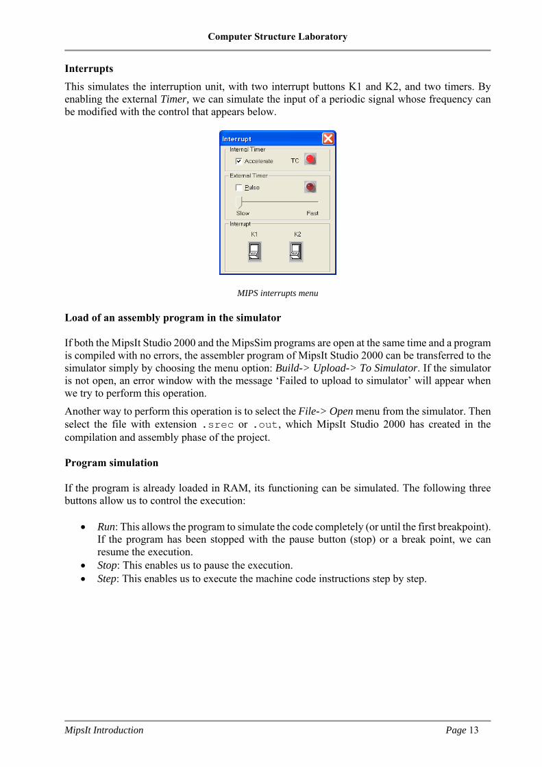
I/O
This module simulates an 8-bit input/output unit. It includes 8 switches (inputs) and 8 LEDs (outputs). The value of the switches can be read when accessing position 0xBF900000 and the output value of the LEDs can be modified by writing also on this position.
8-bit Input/Output
Computer Structure Laboratory
MipsIt Introduction Page 13
Interrupts
This simulates the interruption unit, with two interrupt buttons K1 and K2, and two timers. By enabling the external Timer, we can simulate the input of a periodic signal whose frequency can be modified with the control that appears below.
MIPS interrupts menu
Load of an assembly program in the simulator
If both the MipsIt Studio 2000 and the MipsSim programs are open at the same time and a program is compiled with no errors, the assembler program of MipsIt Studio 2000 can be transferred to the simulator simply by choosing the menu option: Build-> Upload-> To Simulator. If the simulator is not open, an error window with the message ‘Failed to upload to simulator’ will appear when we try to perform this operation.
Another way to perform this operation is to select the File-> Open menu from the simulator. Then select the file with extension .srec or .out, which MipsIt Studio 2000 has created in the compilation and assembly phase of the project.
Program simulation
If the program is already loaded in RAM, its functioning can be simulated. The following three buttons allow us to control the execution:
Run: This allows the program to simulate the code completely (or until the first breakpoint). If the program has been stopped with the pause button (stop) or a break point, we can resume the execution.
Stop: This enables us to pause the execution. Step: This enables us to execute the machine code instructions step by step.
Computer Structure Laboratory
MipsIt Introduction Page 14
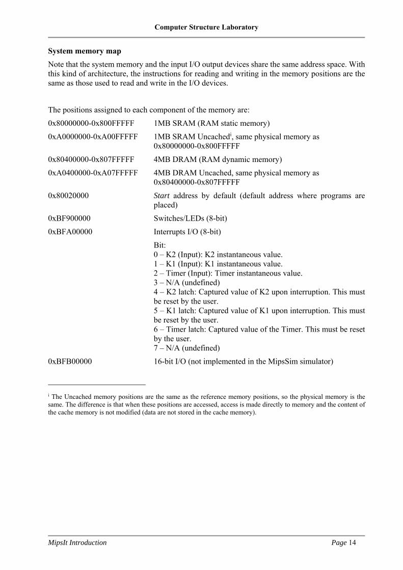
System memory map
Note that the system memory and the input I/O output devices share the same address space. With this kind of architecture, the instructions for reading and writing in the memory positions are the same as those used to read and write in the I/O devices.
The positions assigned to each component of the memory are:
0x80000000-0x800FFFFF 1MB SRAM (RAM static memory)
0xA0000000-0xA00FFFFF 1MB SRAM Uncachedi, same physical memory as 0x80000000-0x800FFFFF
0x80400000-0x807FFFFF 4MB DRAM (RAM dynamic memory)
0xA0400000-0xA07FFFFF 4MB DRAM Uncached, same physical memory as 0x80400000-0x807FFFFF
0x80020000 Start address by default (default address where programs are placed)
0xBF900000 Switches/LEDs (8-bit)
0xBFA00000 Interrupts I/O (8-bit)
Bit: 0 – K2 (Input): K2 instantaneous value. 1 – K1 (Input): K1 instantaneous value. 2 – Timer (Input): Timer instantaneous value. 3 – N/A (undefined) 4 – K2 latch: Captured value of K2 upon interruption. This must be reset by the user. 5 – K1 latch: Captured value of K1 upon interruption. This must be reset by the user. 6 – Timer latch: Captured value of the Timer. This must be reset by the user. 7 – N/A (undefined)
0xBFB00000 16-bit I/O (not implemented in the MipsSim simulator)
i The Uncached memory positions are the same as the reference memory positions, so the physical memory is the same. The difference is that when these positions are accessed, access is made directly to memory and the content of the cache memory is not modified (data are not stored in the cache memory).
Computer Structure Laboratory
Cache Memory (part I) Page 1
Laboratory 2:
Cache Memory (part I) (Updated at 29/01/2019)
Work at home (planned) time: 1:30 h Lab time: 2:30 h
1. Introduction In this second laboratory session we will study the cache memory system and see how it functions when simple programs are executed with regular access patterns to memory. Cache memory performance will be studied while taking into account the mapping algorithm used. We will also analyse several techniques for making programs more efficient. These techniques can significantly reduce the failure rate when a system is run with cache memory. We begin with a description of the MIPS cache memory and the configuration options that are possible in the MipsIt Simulator. We will then use a simple program to show the process involved in compiling and adapting the code to ensure that the experiments we carry out are performed correctly. We will then conduct several experiments in which the characteristics of the cache memory are modified.
Goals On completion of this laboratory session you will be able to:
- understand the possible configurations of the MipsIt cache system, - configure the cache memory module of the MipsIt simulator, - adapt a C program to evaluate the use of the cache memory in the MipsIt, - evaluate the use of the cache memory for a simple program, and - determine the causes of the cache behaviour from the access patterns.
2. Preliminary (pre-lab) work For pre-lab work, all members of the laboratory groups should read Annex I of this document, which describes the cache memory module for the MipsIt simulator. You should also read Annex II, which describes the steps to follow to adapt the example program we use in the laboratory to check the functioning of the cache memory. You also ned to review the concepts on computer memory that were explained in Topic 1. For some questions you must consult some of the bibliographic sources indicated or that are available on the Internet. After reading Annex I and II, answer the following questions:
1. What kind of architecture (Von Neumann or Harvard) is used in the simulated computer, both for the cache memory system and the main memory system?
2. Explain the meaning of the following cache memory configuration parameters: Size, Block Size and Block in sets.
Lab 2
Computer Structure Laboratory
Cache Memory (part I) Page 2
3. Indicate the number of memory positions occupied by each element of the matricesdescribed in the C program shown in Annex II. What characteristic must all startingpositions of the matrix elements have? How many positions separate the beginning of twocontiguous elements of the matrices?
4. Explain whether the contiguous elements (which occupy consecutive positions) in theexample program are elements of the same row or the same column.
5. What is the total size (in bytes) of the matrices in the memory?6. In the example program, the loops are used to access matrices m1 and m2. Is the matrix
read by rows or by columns? Specify whether in each iteration of the internal loop the nextelements of the matrices are in contiguous memory positions.
7. Indicate which instructions of the assembly code in the assembler program of Annex II,obtained as a result of the compilation of the C code perform, enable access to the positionsof the matrices (reading of m1[i][j] and writing of m2[i][j]).
First checkpoint: Answers to the pre-lab questions must be written up and handed in to the lecturer at the beginning of the session. Any questions posed by the lecturer on these or related issues must be answered in the same way.
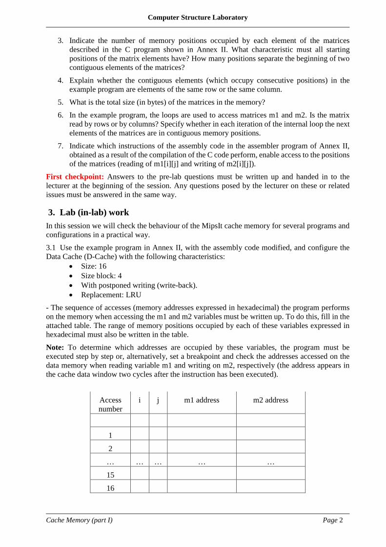
3. Lab (in-lab) workIn this session we will check the behaviour of the MipsIt cache memory for several programs and configurations in a practical way. 3.1 Use the example program in Annex II, with the assembly code modified, and configure the Data Cache (D-Cache) with the following characteristics:
• Size: 16• Size block: 4• With postponed writing (write-back).• Replacement: LRU
- The sequence of accesses (memory addresses expressed in hexadecimal) the program performson the memory when accessing the m1 and m2 variables must be written up. To do this, fill in theattached table. The range of memory positions occupied by each of these variables expressed inhexadecimal must also be written in the table.Note: To determine which addresses are occupied by these variables, the program must be executed step by step or, alternatively, set a breakpoint and check the addresses accessed on the data memory when reading variable m1 and writing on m2, respectively (the address appears in the cache data window two cycles after the instruction has been executed).
Access number
i j m1 address m2 address
1
2
… … … … …
15
16
Computer Structure Laboratory
Cache Memory (part I) Page 3
- Also complete the table below to explain which bits are used for the tag, which bits are used as an index, which are the word selection bits, and which bits are used to select the byte in a line.
Mapping algorithm Tag bits Index bits Word bits Byte bits
Direct (Blocks in set= 1)
K-way associative: 2 ways (Blocks in set=2)
Fully associative (Blocks in set=4)
- Perform several simulations with the mapping algorithms shown in the table below. Then complete the table with the total number of misses and the miss rate obtained from these simulations:
Mapping algorithm Number of misses Miss rate
Direct (Blocks in set= 1)
K-way associative: 2 ways (Blocks in set=2)
Fully associative (Blocks in set=4)
Second checkpoint: Call the lecturer, show them the tables, and answer any questions on their content. 3.2 Now the program will be modified to improve its performance. In this case, the program exchanges the loops that are used to read/write the matrices. The aim is that the matrix should be accessed in the same order in which it is stored in the memory and so the proximity of the program’s spatial references will be increased. To do so, the loops are modified as follows:
#define NUM1 4 int main() { register int i,j; int m1[NUM1][NUM1]; int m2[NUM1][NUM1];
for(i=0;i<NUM1;i++) for(j=0;j<NUM1;j++) m2[i][j]=m1[i][j]; }
- The program must be compiled to obtain the assembly code, eliminate the remaining lines, and the same modifications should be made as in the previous section. Once the executable final code has been obtained, it must be loaded into the simulator. Simulations must then be repeated for the same types of data caches, as in the previous case. - The sequence of accesses to memory performed when variables m1 and m2 are accessed must be monitored. To do so, complete a table as in 3.1.
Computer Structure Laboratory
Cache Memory (part I) Page 4
- The following table must also be completed with the total number of misses and the miss rate obtained from the simulations:
Mapping algorithm Number of misses Miss rate
Direct (Blocks in set= 1)
K-way associative: 2 ways (Blocks in set=2)
Fully associative (Blocks in set=4)
Which mapping algorithms are more suitable for this algorithm?
3.3 After obtaining the experimental data, answer the following questions with reasoned arguments: - Explain why the failure rate for the second algorithm decreases in comparison with the first algorithm. Hint: to discover why this technique works better, compare the access pattern and the state of the cache memory after each iteration of the loops. - Does any mapping algorithm not improve its failure rate for the second algorithm? Explain why. Hint: check which line of the cache memory is assigned to the blocks of different matrices in the same iteration of the loop. - The simulation must be repeated with 2-way associative mapping using the following program:
#define NUM1 4 int main() { register int i,j; int m1[NUM1][NUM1]; int m2[NUM1][NUM1]; int m3[NUM1][NUM1]; int m4[NUM1][NUM1];
for(i=0;i<NUM1;i++) for(j=0;j<NUM1;j++) m4[i][j]=m1[i][j]+m2[i][j]+m3[i][j]; }
Write down the results, compare them against the original algorithm, and suggest an explanation for this behaviour. The program simulation must be repeated with a random replacement algorithm instead of LRU. Does this change anything? Why (not)? Third checkpoint: Call the instructor and show the results of points 3.2 and 3.3. Answer any questions on these results.
Computer Structure Laboratory
Cache Memory (part I) Page 5
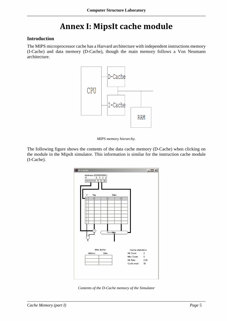
Annex I: MipsIt cache module Introduction The MIPS microprocessor cache has a Harvard architecture with independent instructions memory (I-Cache) and data memory (D-Cache), though the main memory follows a Von Neumann architecture.
MIPS memory hierarchy.
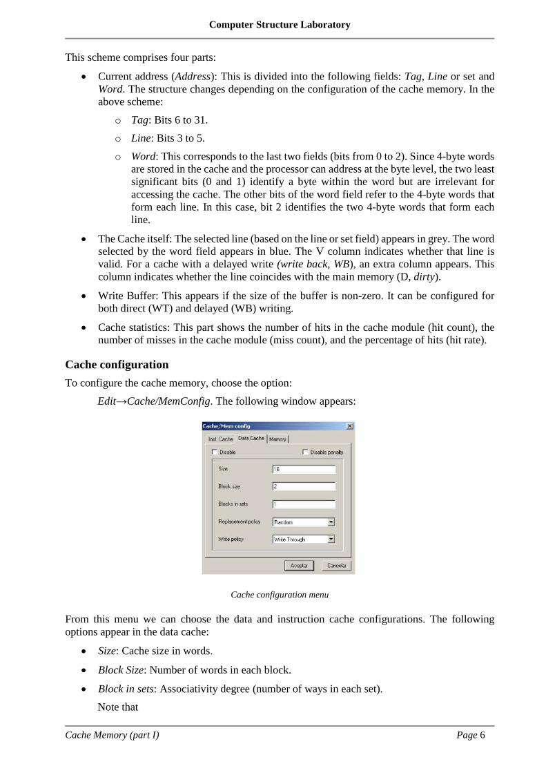
The following figure shows the contents of the data cache memory (D-Cache) when clicking on the module in the MipsIt simulator. This information is similar for the instruction cache module (I-Cache).
Contents of the D-Cache memory of the Simulator
Computer Structure Laboratory
Cache Memory (part I) Page 6
This scheme comprises four parts:
• Current address (Address): This is divided into the following fields: Tag, Line or set and Word. The structure changes depending on the configuration of the cache memory. In the above scheme:
o Tag: Bits 6 to 31. o Line: Bits 3 to 5. o Word: This corresponds to the last two fields (bits from 0 to 2). Since 4-byte words
are stored in the cache and the processor can address at the byte level, the two least significant bits (0 and 1) identify a byte within the word but are irrelevant for accessing the cache. The other bits of the word field refer to the 4-byte words that form each line. In this case, bit 2 identifies the two 4-byte words that form each line.
• The Cache itself: The selected line (based on the line or set field) appears in grey. The word selected by the word field appears in blue. The V column indicates whether that line is valid. For a cache with a delayed write (write back, WB), an extra column appears. This column indicates whether the line coincides with the main memory (D, dirty).
• Write Buffer: This appears if the size of the buffer is non-zero. It can be configured for both direct (WT) and delayed (WB) writing.
• Cache statistics: This part shows the number of hits in the cache module (hit count), the number of misses in the cache module (miss count), and the percentage of hits (hit rate).
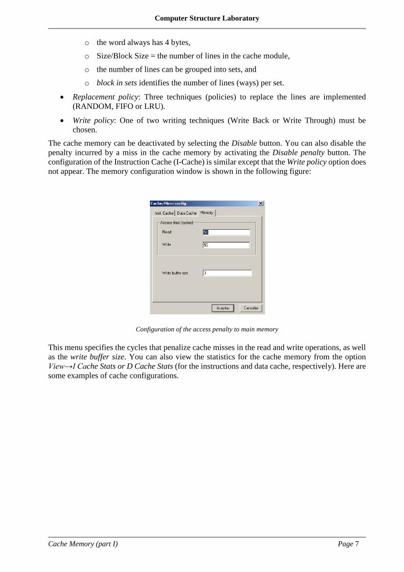
Cache configuration To configure the cache memory, choose the option: Edit→Cache/MemConfig. The following window appears:
Cache configuration menu
From this menu we can choose the data and instruction cache configurations. The following options appear in the data cache:
• Size: Cache size in words.
• Block Size: Number of words in each block.
• Block in sets: Associativity degree (number of ways in each set). Note that
Computer Structure Laboratory
Cache Memory (part I) Page 7
o the word always has 4 bytes, o Size/Block Size = the number of lines in the cache module, o the number of lines can be grouped into sets, and o block in sets identifies the number of lines (ways) per set.
• Replacement policy: Three techniques (policies) to replace the lines are implemented (RANDOM, FIFO or LRU).
• Write policy: One of two writing techniques (Write Back or Write Through) must be chosen.
The cache memory can be deactivated by selecting the Disable button. You can also disable the penalty incurred by a miss in the cache memory by activating the Disable penalty button. The configuration of the Instruction Cache (I-Cache) is similar except that the Write policy option does not appear. The memory configuration window is shown in the following figure:
Configuration of the access penalty to main memory
This menu specifies the cycles that penalize cache misses in the read and write operations, as well as the write buffer size. You can also view the statistics for the cache memory from the option View→I Cache Stats or D Cache Stats (for the instructions and data cache, respectively). Here are some examples of cache configurations.
Computer Structure Laboratory
Cache Memory (part I) Page 8
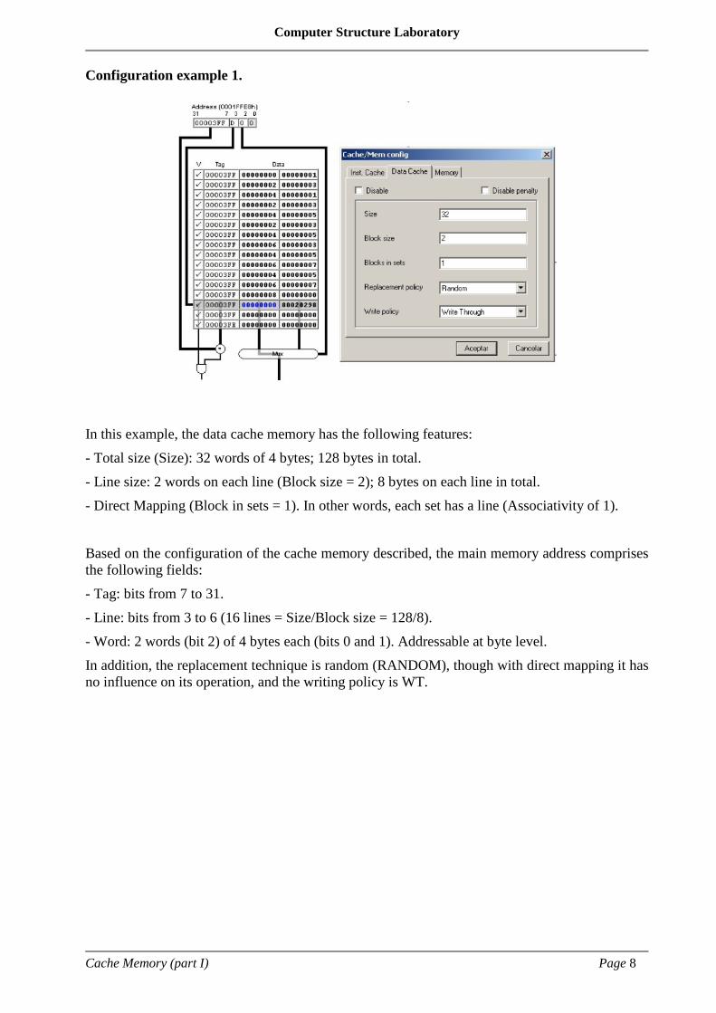
Configuration example 1.
In this example, the data cache memory has the following features: - Total size (Size): 32 words of 4 bytes; 128 bytes in total. - Line size: 2 words on each line (Block size = 2); 8 bytes on each line in total. - Direct Mapping (Block in sets = 1). In other words, each set has a line (Associativity of 1). Based on the configuration of the cache memory described, the main memory address comprises the following fields: - Tag: bits from 7 to 31. - Line: bits from 3 to 6 (16 lines = Size/Block size = 128/8). - Word: 2 words (bit 2) of 4 bytes each (bits 0 and 1). Addressable at byte level. In addition, the replacement technique is random (RANDOM), though with direct mapping it has no influence on its operation, and the writing policy is WT.
Computer Structure Laboratory
Cache Memory (part I) Page 9
Configuration example 2
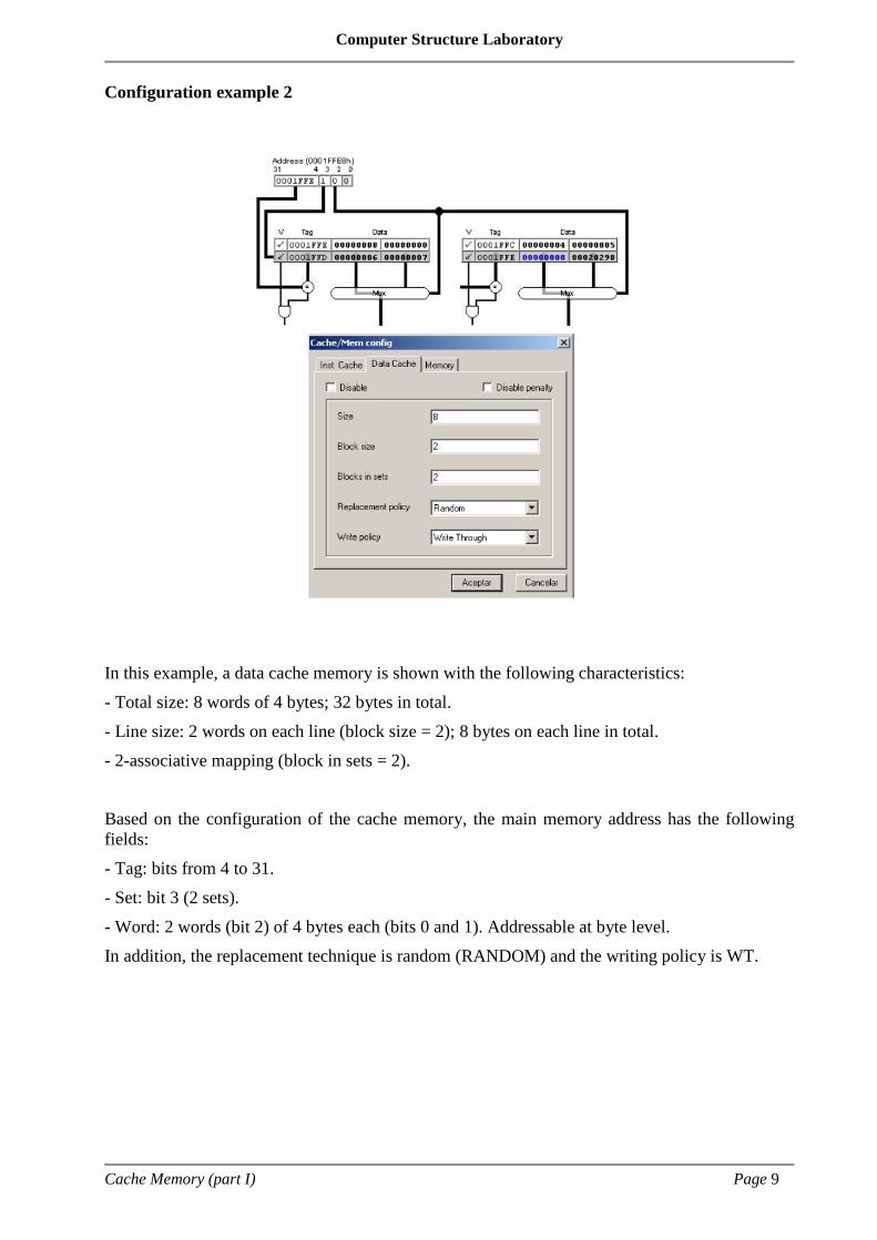
In this example, a data cache memory is shown with the following characteristics: - Total size: 8 words of 4 bytes; 32 bytes in total. - Line size: 2 words on each line (block size = 2); 8 bytes on each line in total. - 2-associative mapping (block in sets = 2). Based on the configuration of the cache memory, the main memory address has the following fields: - Tag: bits from 4 to 31. - Set: bit 3 (2 sets). - Word: 2 words (bit 2) of 4 bytes each (bits 0 and 1). Addressable at byte level. In addition, the replacement technique is random (RANDOM) and the writing policy is WT.
Computer Structure Laboratory
Cache Memory (part I) Page 10
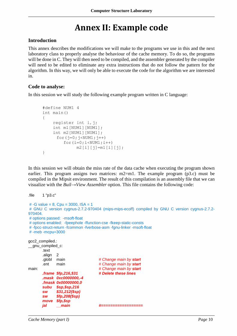
Annex II: Example code Introduction This annex describes the modifications we will make to the programs we use in this and the next laboratory class to properly analyse the behaviour of the cache memory. To do so, the programs will be done in C. They will then need to be compiled, and the assembler generated by the compiler will need to be edited to eliminate any extra instructions that do not follow the pattern for the algorithm. In this way, we will only be able to execute the code for the algorithm we are interested in.
Code to analyse: In this session we will study the following example program written in C language:
#define NUM1 4 int main() { register int i,j; int m1[NUM1][NUM1]; int m2[NUM1][NUM1];
for(j=0;j<NUM1;j++) for(i=0;i<NUM1;i++) m2[i][j]=m1[i][j]; }
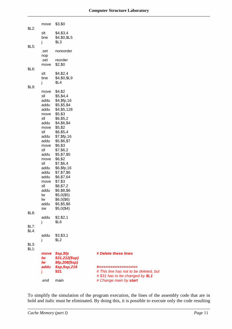
In this session we will obtain the miss rate of the data cache when executing the program shown earlier. This program assigns two matrices: m2=m1. The example program (p3.c) must be compiled in the Mipsit environment. The result of this compilation is an assembly file that we can visualize with the Buil→View Assembler option. This file contains the following code: .file 1 "p3.c" # -G value = 8, Cpu = 3000, ISA = 1 # GNU C version cygnus-2.7.2-970404 (mips-mips-ecoff) compiled by GNU C version cygnus-2.7.2-970404. # options passed: -msoft-float # options enabled: -fpeephole -ffunction-cse -fkeep-static-consts # -fpcc-struct-return -fcommon -fverbose-asm -fgnu-linker -msoft-float # -meb -mcpu=3000 gcc2_compiled.: __gnu_compiled_c: .text .align 2 .globl main # Change main by start .ent main # Change main by start main: # Change main by start .frame $fp,216,$31 # Delete these lines .mask 0xc0000000,-4 .fmask 0x00000000,0 subu $sp,$sp,216 sw $31,212($sp) sw $fp,208($sp) move $fp,$sp jal __main #==================
Computer Structure Laboratory
Cache Memory (part I) Page 11
move $3,$0 $L2: slt $4,$3,4 bne $4,$0,$L5 j $L3 $L5: .set noreorder nop .set reorder move $2,$0 $L6: slt $4,$2,4 bne $4,$0,$L9 j $L4 $L9: move $4,$2 sll $5,$4,4 addu $4,$fp,16 addu $5,$5,$4 addu $4,$5,128 move $5,$3 sll $6,$5,2 addu $4,$6,$4 move $5,$2 sll $6,$5,4 addu $7,$fp,16 addu $5,$6,$7 move $6,$3 sll $7,$6,2 addu $5,$7,$5 move $6,$2 sll $7,$6,4 addu $6,$fp,16 addu $7,$7,$6 addu $6,$7,64 move $7,$3 sll $8,$7,2 addu $6,$8,$6 lw $5,0($5) lw $6,0($6) addu $5,$5,$6 sw $5,0($4) $L8: addu $2,$2,1 j $L6 $L7: $L4: addu $3,$3,1 j $L2 $L3: $L1: move $sp,$fp # Delete these lines lw $31,212($sp) lw $fp,208($sp) addu $sp,$sp,216 #================= j $31 # This line has not to be deleted, but
# $31 has to be changed by $L1 .end main # Change main by start
To simplify the simulation of the program execution, the lines of the assembly code that are in bold and italic must be eliminated. By doing this, it is possible to execute only the code resulting
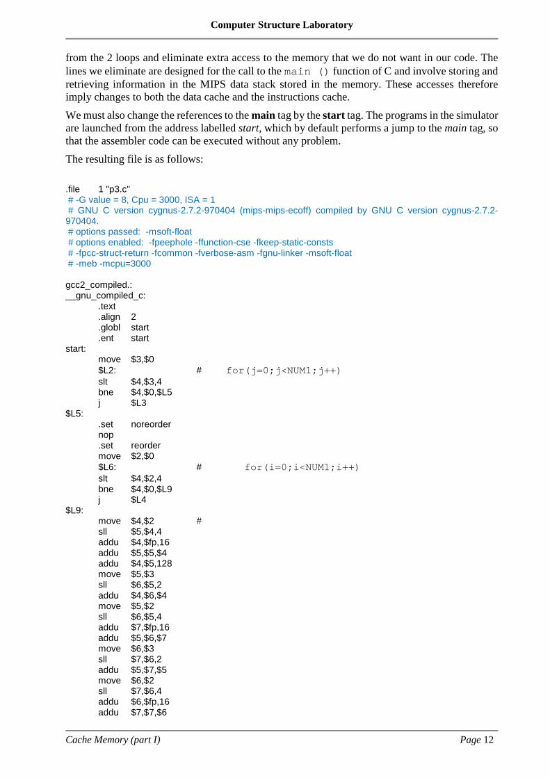
Computer Structure Laboratory
Cache Memory (part I) Page 12
from the 2 loops and eliminate extra access to the memory that we do not want in our code. The lines we eliminate are designed for the call to the main () function of C and involve storing and retrieving information in the MIPS data stack stored in the memory. These accesses therefore imply changes to both the data cache and the instructions cache. We must also change the references to the main tag by the start tag. The programs in the simulator are launched from the address labelled start, which by default performs a jump to the main tag, so that the assembler code can be executed without any problem. The resulting file is as follows: .file 1 "p3.c" # -G value = 8, Cpu = 3000, ISA = 1 # GNU C version cygnus-2.7.2-970404 (mips-mips-ecoff) compiled by GNU C version cygnus-2.7.2-970404. # options passed: -msoft-float # options enabled: -fpeephole -ffunction-cse -fkeep-static-consts # -fpcc-struct-return -fcommon -fverbose-asm -fgnu-linker -msoft-float # -meb -mcpu=3000 gcc2_compiled.: __gnu_compiled_c: .text .align 2 .globl start .ent start start: move $3,$0
$L2: # for(j=0;j<NUM1;j++) slt $4,$3,4 bne $4,$0,$L5 j $L3 $L5: .set noreorder nop .set reorder move $2,$0
$L6: # for(i=0;i<NUM1;i++) slt $4,$2,4 bne $4,$0,$L9 j $L4 $L9: move $4,$2 # sll $5,$4,4 addu $4,$fp,16 addu $5,$5,$4 addu $4,$5,128 move $5,$3 sll $6,$5,2 addu $4,$6,$4 move $5,$2 sll $6,$5,4 addu $7,$fp,16 addu $5,$6,$7 move $6,$3 sll $7,$6,2 addu $5,$7,$5 move $6,$2 sll $7,$6,4 addu $6,$fp,16 addu $7,$7,$6
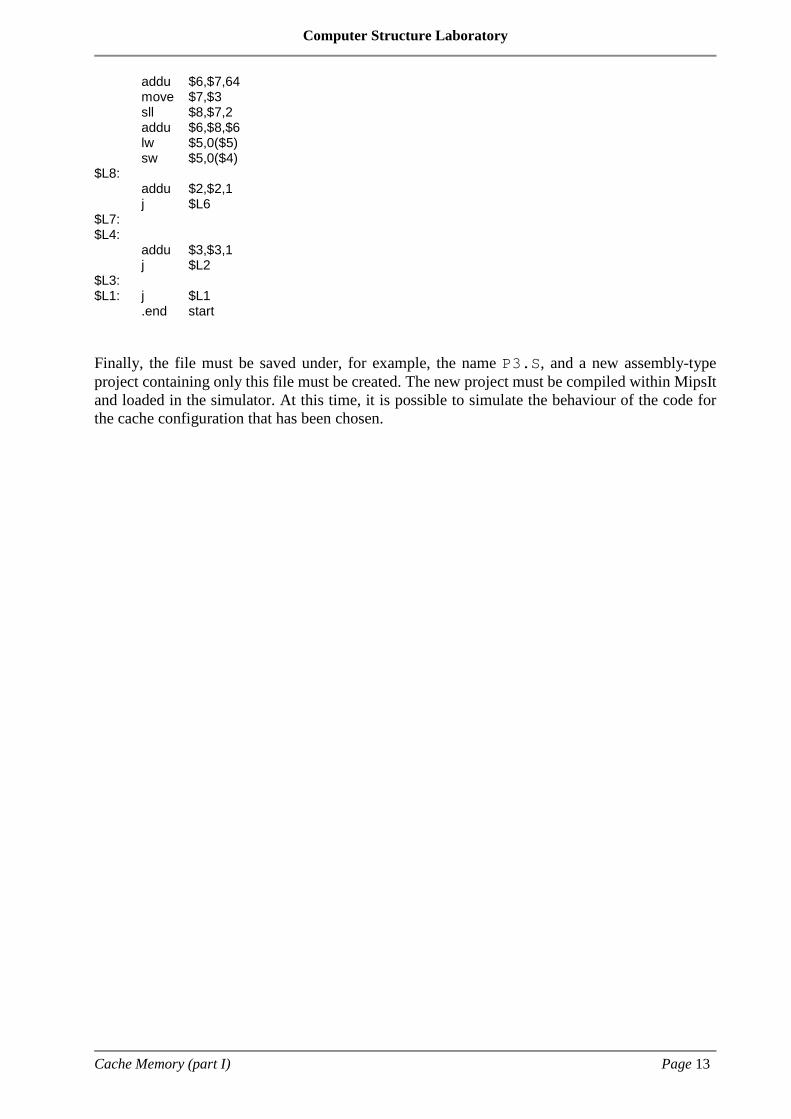
Computer Structure Laboratory
Cache Memory (part I) Page 13
addu $6,$7,64 move $7,$3 sll $8,$7,2 addu $6,$8,$6 lw $5,0($5) sw $5,0($4) $L8: addu $2,$2,1 j $L6 $L7: $L4: addu $3,$3,1 j $L2 $L3: $L1: j $L1 .end start
Finally, the file must be saved under, for example, the name P3.S, and a new assembly-type project containing only this file must be created. The new project must be compiled within MipsIt and loaded in the simulator. At this time, it is possible to simulate the behaviour of the code for the cache configuration that has been chosen.
Computer Structure Laboratory
Cache Memory: Software optimizations Page 1
Laboratory 3:
Cache Memory (part II): Software Optimizations
(Updated at 29/01/2019) Work at home (planned) time: 1:30 h
Lab time: 2:30 h
1. Introduction In this laboratory session we will study the cache memory system and its behaviour by optimizing simple algorithms related to typical access patterns in numerous applications. The behaviour of the cache memory will be studied depending on the mapping algorithm used. We also explain how the system responds to the various optimization techniques. In the previous laboratory class, we studied an example of software optimization on an algorithm that added two matrices. The example showed how the miss rate was affected exchanging the loops that are used to read and write the matrices. It is important to establish a workgroup dynamic that enables you to take maximum profit from your time in the laboratory. For this reason, you should arrive at the laboratory on time and pay attention to your lecturer’s instructions.
Goals On completion of this session you will be able to - understand the software optimization techniques that enable the cache memory to perform better, - evaluate the behaviour of the most common optimization techniques for different configurations of the cache memory, - apply software optimization techniques to their algorithms, and - predict how the cache memory will function with the proposed algorithms before applying the proposed optimizations techniques.
Materials We will use the same software as in the two previous laboratory sessions (P1 and P2).
Lab 3
Computer Structure Laboratory
Cache Memory: Software optimizations Page 2
2. Preliminary (pre-lab) workFor the pre-lab work for this session, all members of the workgroups must read Annex I of this document, which describes the most common software optimization techniques for extracting the greatest benefit from the cache system. You should also review the main concepts of memory we have studied in class so far. After reading Annex I and reviewing the memory subject, answer the following questions:
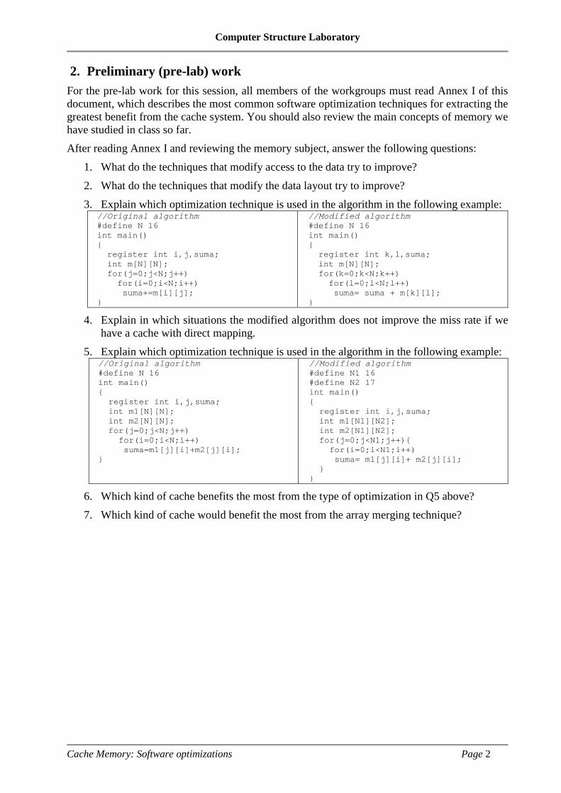
1. What do the techniques that modify access to the data try to improve?2. What do the techniques that modify the data layout try to improve?3. Explain which optimization technique is used in the algorithm in the following example:
//Original algorithm #define N 16 int main() { register int i,j,suma; int m[N][N]; for(j=0;j<N;j++) for(i=0;i<N;i++) suma+=m[i][j]; }
//Modified algorithm #define N 16 int main() { register int k,l,suma; int m[N][N]; for(k=0;k<N;k++) for(l=0;l<N;l++) suma= suma + m[k][l]; }
4. Explain in which situations the modified algorithm does not improve the miss rate if wehave a cache with direct mapping.
5. Explain which optimization technique is used in the algorithm in the following example://Original algorithm #define N 16 int main() { register int i,j,suma; int m1[N][N]; int m2[N][N]; for(j=0;j<N;j++) for(i=0;i<N;i++) suma=m1[j][i]+m2[j][i]; }
//Modified algorithm #define N1 16 #define N2 17 int main() { register int i,j,suma; int m1[N1][N2]; int m2[N1][N2]; for(j=0;j<N1;j++){ for(i=0;i<N1;i++) suma= m1[j][i]+ m2[j][i]; } }
6. Which kind of cache benefits the most from the type of optimization in Q5 above?7. Which kind of cache would benefit the most from the array merging technique?
Computer Structure Laboratory
Cache Memory: Software optimizations Page 3
3. Lab (in-lab) work In this laboratory session, we will check, in a practical way, the behaviour of the cache memory after several optimizations have been applied to the algorithm we used in the previous session. You must therefore bring to this laboratory session a copy of the results you obtained in that one. 3.1 Using the matrix addition algorithm shown below, modify the algorithm using the array padding technique.
#define NUM 4 int main() { register int i,j; /* variables are stored in registers*/ int m1[NUM][NUM]; int m2[NUM][NUM]; int m3[NUM][NUM]; int m4[NUM][NUM]; for(i=0;i<NUM;i++) for(j=0;j<NUM;j++) m4[i][j]=m1[i][j]+m2[i][j]+m3[i][j]; }
The program must be compiled to obtain the assembly code. Then edit this code to eliminate several lines and change some labels as we did in the previous laboratory session. When the code is ready, upload it to the simulator. The data cache must also be configured with the following parameters:
• Size: 16
• Block size: 4
• With delayed writing (write-back)
• Replacement algorithm: LRU - Indicate the sequence of accesses (memory addresses expressed in hexadecimal) the program performs on the memory when it accesses variables m1, m2, m3 and m4. To do so, fill in the table below. Also indicate (in hexadecimal) the range of memory positions occupied by each of these variables.
Access number
i j m1 address m2 address m3 address m4 address
1
2
… … … … … …
15
16
- Several simulations with cache memories with different mapping algorithms should be performed to complete the following table with the total number of misses and the miss rate obtained from
Computer Structure Laboratory
Cache Memory: Software optimizations Page 4
the simulations for the two algorithms (the original one and the algorithm improved with array padding):
Mapping algorithm Number of misses Miss rate Direct (Blocks in set= 1) K-way associative: 2 ways (Blocks in set=2)
Fully associative (Blocks in set=4)
- The results must be compared and understood for each mapping algorithm. The original algorithm must be compared to the one improved by array padding. - Using the same original algorithm, the replacement algorithm of the cache memory must be changed to Random. Several simulations must be performed to complete the following table with the total number of misses and the miss rate obtained by the simulations:
Mapping algorithm Number of misses Miss rate
K-way associative: 2 ways (Blocks in set=2)
Fully associative (Blocks in set=4)
8. Explain the differences obtained in both cases (LRU and Random). First checkpoint: Call the lecturer, show them the tables, and answer any questions on their content. 3.2 In this second section, the original program must be modified using the array merging technique. The code execution must be simulated by following the same steps as in section 3.1.
- Indicate the sequence of accesses: memory addresses expressed in hexadecimal that the program performs on the memory when accessing variables m[][].m1, m[][].m2, m[][].m3 and m[][].m4. To do so, complete the attached table. Similarly, write down the range of memory positions occupied by each of these variables, expressed in hexadecimal.
Access number
i j .m1 address .m2 address .m3 address .m4 address
1
2
… … … … … …
15
16
Computer Structure Laboratory
Cache Memory: Software optimizations Page 5
- Perform simulations with caches with different mapping algorithms using the configuration of the cache memory proposed in the previous section. Complete the following table with the total number of misses and the miss rate obtained by the simulations:
Mapping algorithm Number of misses Miss rate
Direct (Blocks in set= 1)
K-way associative: 2 ways (Blocks in set=2)
Fully associative (Blocks in set=4)
9. Compare and explain the results obtained with different cache mapping algorithms, the
original algorithm, and the algorithm modified with array merging. 10. Does the replacement algorithm (LRU or Random) have any effect? To determine this, you
need to perform simulations with these replacement algorithms.
Second checkpoint: Call the lecturer, show them the tables, and answer any questions on their content.
Answers to the preliminary questions (1 to 7) and questions 8, 9 and 10 must be written up and handed in to the lecturer before you leave the laboratory.
Computer Structure Laboratory
Cache Memory: Software optimizations Page 6
Annex I: Basic techniques of software optimization
Introduction The memory hierarchy enables us to hide both the low bandwidth and the latency of the main memory, which are slow in comparison with current CPUs. For this reason, the cache memory located between the main memory and the CPU is used. Unfortunately, as the cache size is limited, it only stores copies of recently used data. Normally, when new data are loaded into the cache memory, older data must be replaced. Cache memory reduces the program execution time because a program follows the principle of locality. We must therefore design algorithms that follow both spatial and temporal localities. In this document we will present several basic techniques that will help us to design algorithms that improve cache memory utilization. These techniques will be based on transforming the original algorithm. The idea is to modify the data access arrangement or the data storage itself in order to improve the locality of temporal and spatial reference. Below we describe some of the most useful techniques.
Data access optimizations The aim of data access optimizations is to improve the locality of data. For this, modifications are made to the loops of the algorithms, which are often nested, so that at each iteration data used in the preceding iterations are reused or, similarly, data close to the used ones, which have been copied in the cache in immediately preceding iterations, are accessed. We now present a set of transformations aimed at improving spatial locality for a cache level (L1) in the memory hierarchy. Loop interchange Using this technique, the program is modified to improve its performance. In this case, the program exchanges the loops that are used to go through the matrices. The aim is for the matrix be accessed in the same order in which it is stored in the memory, thus increasing the spatial proximity of the references in the program. This technique can only be used if the order of the loops is not important. When the loop interchange technique is generalized to more than two loops, it is called loop permutation. In this case, two loops of the algorithm can be exchanged without being adjacent. To illustrate this technique, we will use a matrix addition example. In this algorithm, all the elements of two matrices (m1 and m2) are read and added, and the result obtained is assigned to a third matrix (m3). The sentence is as follows:
m3[i][j]=m1[i][j]+m2[i][j];
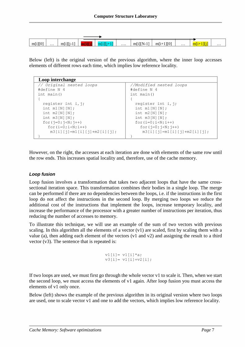
We must go through the rows and columns of the matrices to access their elements. However, the elements of a matrix are stored in the memory following an order of consecutive rows (C code) or columns (Fortran code). In the case of C language, the element m[i][j+1] of a matrix is next to the element m[i][j], while the element m [i+1][j] is a row away from m[i][j] (i.e. N positions away, where N is the number of elements in a row).
Computer Structure Laboratory
Cache Memory: Software optimizations Page 7
Below (left) is the original version of the previous algorithm, where the inner loop accesses elements of different rows each time, which implies low reference locality.
Loop interchange // Original nested loops #define N 4 int main() { register int i,j; int m1[N][N]; int m2[N][N]; int m3[N][N]; for(j=0;j<N;j++) for(i=0;i<N;i++) m3[i][j]=m1[i][j]+m2[i][j]; }
//Modified nested loops #define N 4 int main() { register int i,j; int m1[N][N]; int m2[N][N]; int m3[N][N]; for(i=0;i<N;i++) for(j=0;j<N;j++) m3[i][j]=m1[i][j]+m2[i][j]; }
However, on the right, the accesses at each iteration are done with elements of the same row until the row ends. This increases spatial locality and, therefore, use of the cache memory. Loop fusion Loop fusion involves a transformation that takes two adjacent loops that have the same cross-sectional iteration space. This transformation combines their bodies in a single loop. The merge can be performed if there are no dependencies between the loops, i.e. if the instructions in the first loop do not affect the instructions in the second loop. By merging two loops we reduce the additional cost of the instructions that implement the loops, increase temporary locality, and increase the performance of the processor with a greater number of instructions per iteration, thus reducing the number of accesses to memory. To illustrate this technique, we will use an example of the sum of two vectors with previous scaling. In this algorithm all the elements of a vector (v1) are scaled, first by scaling them with a value (a), then adding each element of the vectors (v1 and v2) and assigning the result to a third vector (v3). The sentence that is repeated is:
v1[i]= v1[i]*a; v3[i]= v1[i]+v2[i];
If two loops are used, we must first go through the whole vector v1 to scale it. Then, when we start the second loop, we must access the elements of v1 again. After loop fusion you must access the elements of v1 only once. Below (left) shows the example of the previous algorithm in its original version where two loops are used, one to scale vector v1 and one to add the vectors, which implies low reference locality.
m[i][0] … m[i][j-1] m[i][j] m[i][j+1] …. m[i][N-1] m[i+1][0] … m[i+1][j] …
Computer Structure Laboratory
Cache Memory: Software optimizations Page 8
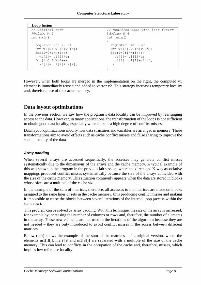
Loop fusion // Original code #define N 4 int main() { register int i, a; int v1[N],v2[N]v3[N]; for(i=0;i<N;i++) v1[i]= v1[i]*a; for(i=0;i<N;i++) v3[i]= v1[i]+v2[i]; }
// Modified code with loop fusion #define N 4 int main() { register int i,a; int v1[N],v2[N]v3[N]; for(i=0;i<N;i++){ v1[i]= v1[i]*a; v3[i]= v1[i]+v2[i]; } }
However, when both loops are merged in the implementation on the right, the computed v1 element is immediately reused and added to vector v2. This strategy increases temporary locality and, therefore, use of the cache memory.
Data layout optimizations In the previous section we saw how the program’s data locality can be improved by rearranging access to the data. However, in many applications, the transformation of the loops is not sufficient to obtain good data locality, especially when there is a high degree of conflict misses. Data layout optimizations modify how data structures and variables are arranged in memory. These transformations aim to avoid effects such as cache conflict misses and false sharing to improve the spatial locality of the data. Array padding
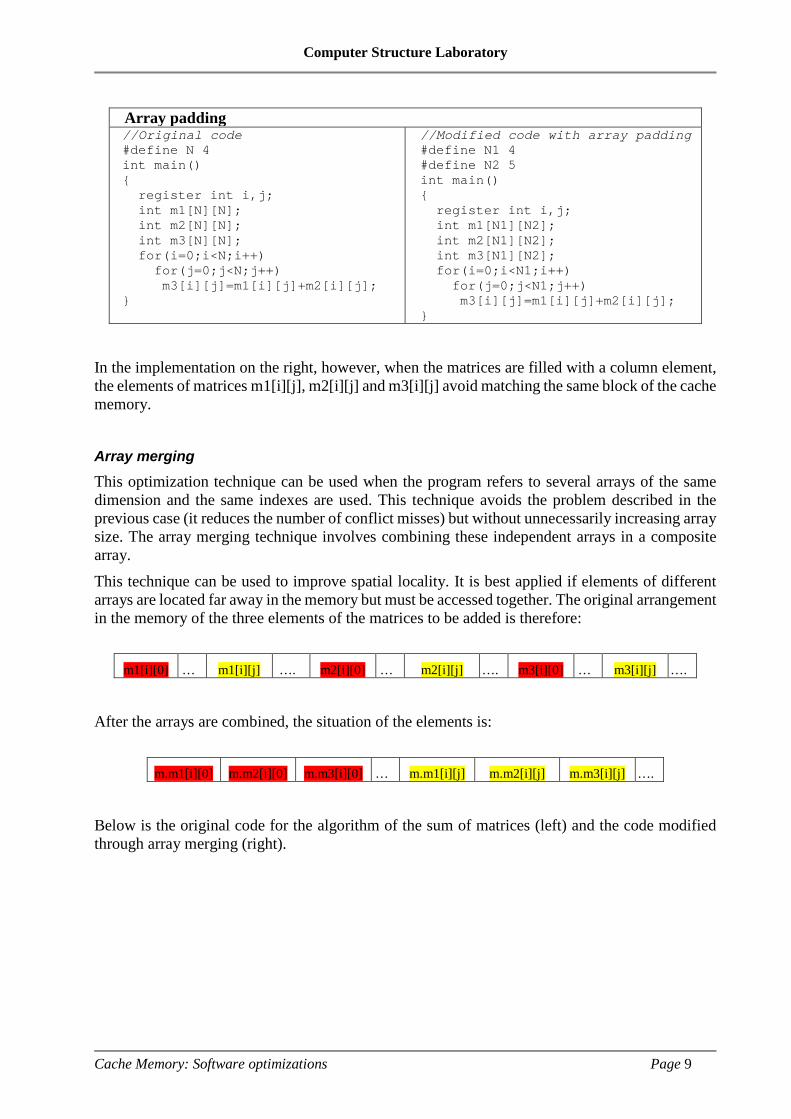
When several arrays are accessed sequentially, the accesses may generate conflict misses systematically due to the dimensions of the arrays and the cache memory. A typical example of this was shown in the program in the previous lab session, where the direct and K-way associative mappings produced conflict misses systematically because the size of the arrays coincided with the size of the cache memory. This situation commonly appears when the data are stored in blocks whose sizes are a multiple of the cache size. In the example of the sum of matrices, therefore, all accesses to the matrices are made on blocks assigned to the same lines or sets in the cache memory, thus producing conflict misses and making it impossible to reuse the blocks between several iterations of the internal loop (access within the same row). This problem can be solved by array padding. With this technique, the size of the array is increased, for example by increasing the number of columns or rows and, therefore, the number of elements in the array. These new elements are not used in the iterations of the algorithm because they are not needed – they are only introduced to avoid conflict misses in the access between different matrices. Below (left) shows the example of the sum of the matrices in its original version, where the elements m1[i][j], m2[i][j] and m3[i][j] are separated with a multiple of the size of the cache memory. This can lead to conflicts in the occupation of the cache and, therefore, misses, which implies low reference locality.
Computer Structure Laboratory
Cache Memory: Software optimizations Page 9
Array padding //Original code #define N 4 int main() { register int i,j; int m1[N][N]; int m2[N][N]; int m3[N][N]; for(i=0;i<N;i++) for(j=0;j<N;j++) m3[i][j]=m1[i][j]+m2[i][j]; }
//Modified code with array padding #define N1 4 #define N2 5 int main() { register int i,j; int m1[N1][N2]; int m2[N1][N2]; int m3[N1][N2]; for(i=0;i<N1;i++) for(j=0;j<N1;j++) m3[i][j]=m1[i][j]+m2[i][j]; }
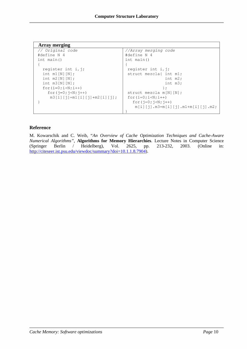
In the implementation on the right, however, when the matrices are filled with a column element, the elements of matrices m1[i][j], m2[i][j] and m3[i][j] avoid matching the same block of the cache memory. Array merging This optimization technique can be used when the program refers to several arrays of the same dimension and the same indexes are used. This technique avoids the problem described in the previous case (it reduces the number of conflict misses) but without unnecessarily increasing array size. The array merging technique involves combining these independent arrays in a composite array. This technique can be used to improve spatial locality. It is best applied if elements of different arrays are located far away in the memory but must be accessed together. The original arrangement in the memory of the three elements of the matrices to be added is therefore:
m1[i][0] … m1[i][j] …. m2[i][0] … m2[i][j] …. m3[i][0] … m3[i][j] ….
After the arrays are combined, the situation of the elements is:
m.m1[i][0] m.m2[i][0] m.m3[i][0] … m.m1[i][j] m.m2[i][j] m.m3[i][j] ….
Below is the original code for the algorithm of the sum of matrices (left) and the code modified through array merging (right).
Computer Structure Laboratory
Cache Memory: Software optimizations Page 10
Array merging // Original code #define N 4 int main() { register int i,j; int m1[N][N]; int m2[N][N]; int m3[N][N]; for(i=0;i<N;i++) for(j=0;j<N;j++) m3[i][j]=m1[i][j]+m2[i][j]; }
//Array merging code #define N 4 int main() { register int i,j; struct mezcla{ int m1; int m2; int m3; }; struct mezcla m[N][N]; for(i=0;i<N;i++) for(j=0;j<N;j++) m[i][j].m3=m[i][j].m1+m[i][j].m2; }
Reference M. Kowarschik and C. Weib, “An Overview of Cache Optimization Techniques and Cache-Aware Numerical Algorithms”, Algorithms for Memory Hierarchies. Lecture Notes in Computer Science (Springer Berlin / Heidelberg), Vol. 2625, pp. 213-232, 2003. (Online in: http://citeseer.ist.psu.edu/viewdoc/summary?doi=10.1.1.8.7904).
Computer Structure Laboratory
I/O system: Polled I/O Page 1
Laboratory 4:
Input/Output System (I): Polling (Software-driven I/O)
(Updated at 29/01/2019) Work at home (planned) time: 1:30 h
Lab time: 2:30 h
1. Introduction In this laboratory session we will study the computer input/output system and the synchronization technique of peripheral devices based on polling, also called software-driven I/O. This will enable us to also study how to access the status information of peripheral devices.
Goals On completion of this session you will be able to: - understand techniques for checking and modifying the status information of a peripheral, - design algorithms to check the value of the status bits of a peripheral and respond accordingly, - use bitwise operators (in C code) to check and modify the flags of a register, - implement C programs to control the input/output of the MipsIT I/O modules through polling.
Resources We will use the same software as in previous sessions, i.e. the MipsIt programming environment.
2. Preliminary (pre-lab) work For the pre-lab work for this session, all members of the workgroups should read the first two annexes to this document, which describe the MipsIt I/O space. You should also read Annex III, which describes C operators at bit level. These operators will prove very useful for this practice session. You should also review all the concepts of the computer I/O system you have studied so far in your theory classes. After reading the annexes and the recommended bibliography, answer the following questions:
1. Briefly describe the data transfer synchronization method known as “polling”. 2. Assume that we have a data entry module with a status register (which we call status),
which has a value of 1 when there are data to be read and zero otherwise, and a data I/O register, from which we can read the data of the I/O module. Write a procedure, in pseudo-algorithmic language, that can read the data from that module and write them to a data variable.
3. What sources share the external interrupt line 3 in the MipsIt simulator? 4. What register should we read to check the status of buttons K1 and K2 and the external
Timer signal associated with the MipsIt interrupt module (module 2 in the Annex)?
Lab 4
Computer Structure Laboratory
I/O system: Polled I/O Page 2
5. Describe how, by reading the state of the interrupt module (module 2 in Annex 2), we candetermine whether at a given moment button K2 is being pressed.
6. Describe how, by reading the interrupt module status, we can determine whether the K2button has been pressed. Explain what we should to avoid future false detections.
7. Suggest a sentence or a short C code fragment to detect whether K2 is being pressed. If itis, the value TRUE must be assigned to a Boolean variable.
8. Design a program to implement a shift of 1 LED along the bank of LEDs in module 1(pseudocode or flowchart). First, the program must wait until the K1 button in module 2has been pressed. Then, led0 will turn on and then go to led1 and so on until it reachesled7. At this point, the LED will go backwards by doing the reverse movement until itreaches led0 (Knight Rider style) and then it will start again. The program will end only inthe led0 position if the K2 button has been pressed at any time. The timer must be used tocontrol the LEDs’ lighting time.
First checkpoint: Answers to Q1-Q8 must be written up and handed in to the lecturer at the beginning of the session.
3. Lab (in-lab) workIn this session we will see the programming and management of the I/O modules in a practical way. To do so, we will design several programs that involve the use of these modules.
Second checkpoint: Implement the counter program proposed in question 8 of the pre-lab tasks. Show the proper functioning of the program and code to your lecturer. Bear in mind that the compiler’s default options must be edited as in section 3.1 in P1 since we are accessing the processor's I/O space.
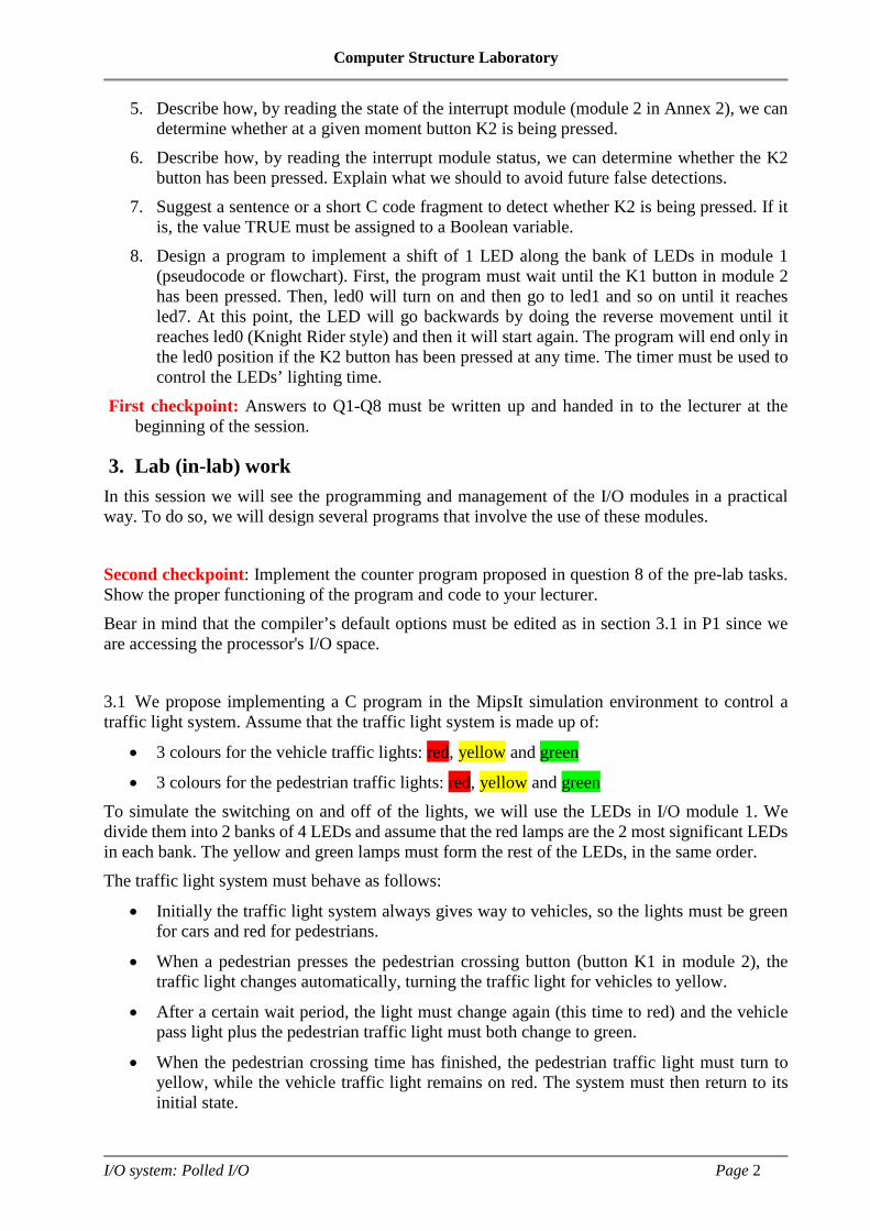
3.1 We propose implementing a C program in the MipsIt simulation environment to control a traffic light system. Assume that the traffic light system is made up of:
• 3 colours for the vehicle traffic lights: red, yellow and green
• 3 colours for the pedestrian traffic lights: red, yellow and greenTo simulate the switching on and off of the lights, we will use the LEDs in I/O module 1. We divide them into 2 banks of 4 LEDs and assume that the red lamps are the 2 most significant LEDs in each bank. The yellow and green lamps must form the rest of the LEDs, in the same order. The traffic light system must behave as follows:
• Initially the traffic light system always gives way to vehicles, so the lights must be greenfor cars and red for pedestrians.
• When a pedestrian presses the pedestrian crossing button (button K1 in module 2), thetraffic light changes automatically, turning the traffic light for vehicles to yellow.
• After a certain wait period, the light must change again (this time to red) and the vehiclepass light plus the pedestrian traffic light must both change to green.
• When the pedestrian crossing time has finished, the pedestrian traffic light must turn toyellow, while the vehicle traffic light remains on red. The system must then return to itsinitial state.
Computer Structure Laboratory
I/O system: Polled I/O Page 3
To set the time in each state, the external timer (located in module 2) must be used. The time in each case must be:
• The yellow light must be On for 5 pulses of the external timer for both vehicles and pedestrians.
• The red light for vehicles (green for pedestrians) must be On for 20 pulses of the external timer.
Bear in mind that the compiler’s default options must be edited as in section 3.1 in P1 since we are accessing the processor’s I/O space. Third checkpoint: The traffic light program must be implemented using the polling synchronization method and simulated within the MipsIt program. Show the proper functioning of the program and the code to your lecturer.
Computer Structure Laboratory
I/O system: Polled I/O Page 4
Annex I: MipsIt I/O memory space Introduction The input/output (I/O) system of a computer consists of the elements (buses, registers, protocols, etc.) that enable us to connect the computer to the peripheral devices. An I/O operation can be divided into three phases:
1. Addressing: Access to the module through its memory address. 2. Synchronization and control of the transfer: The mechanism used to determine whether
the peripheral is ready to begin a transfer (to send or to receive) data, control the transfer, and control whether another transfer can be started.
3. Data transfer: Transfer of the data itself, which may require transforming data sent by the peripherals.
Synchronization is a critical stage in I/O operations and fundamental for correct data transfer. It also has great influence on the final performance of the system. Three commonly used techniques exist: polling (software-driven I/O), interrupts, and direct memory transfer (DMA).
Software-driven or interrupt-based synchronization In the data transfer between the computer and the Input/Output (I/O) module, the CPU is responsible for transferring the memory data and sending them to the I/O module (in a write), or similarly, for storing the data from the I/O module in the memory (in a read). The arrival of data from outside the computer is normally unpredictable and the program cannot know exactly when an I/O module will have available data that must be read. A method is therefore needed to synchronize the execution of the program in the CPU with the I/O modules. Through this synchronization, the I/O module notifies the CPU when data are waiting to be read or when the queue of the data to be written is empty.
Polling (Software-driven) synchronization With this method the CPU executes a program that directly controls the I/O transfer. The program is responsible for sending the order and waits until the data transfer is complete. The program continuously checks the I/O module status until the transfer is complete. The polling is commonly implemented via a loop that does not end until all the data are transferred.
Interrupt-based synchronization Through an interrupt request performed by the interrupt module, the I/O module notifies the CPU that there are data to transfer. However, the CPU is responsible for extracting the data from the module (in the case of reading) or for sending the data to the module (in case of writing). As in the previous case, therefore, each of the transferred data passes through the CPU.
Computer Structure Laboratory
I/O system: Polled I/O Page 5
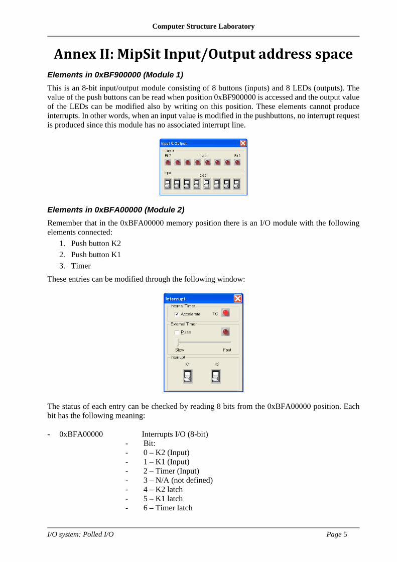
Annex II: MipSit Input/Output address space Elements in 0xBF900000 (Module 1) This is an 8-bit input/output module consisting of 8 buttons (inputs) and 8 LEDs (outputs). The value of the push buttons can be read when position 0xBF900000 is accessed and the output value of the LEDs can be modified also by writing on this position. These elements cannot produce interrupts. In other words, when an input value is modified in the pushbuttons, no interrupt request is produced since this module has no associated interrupt line.
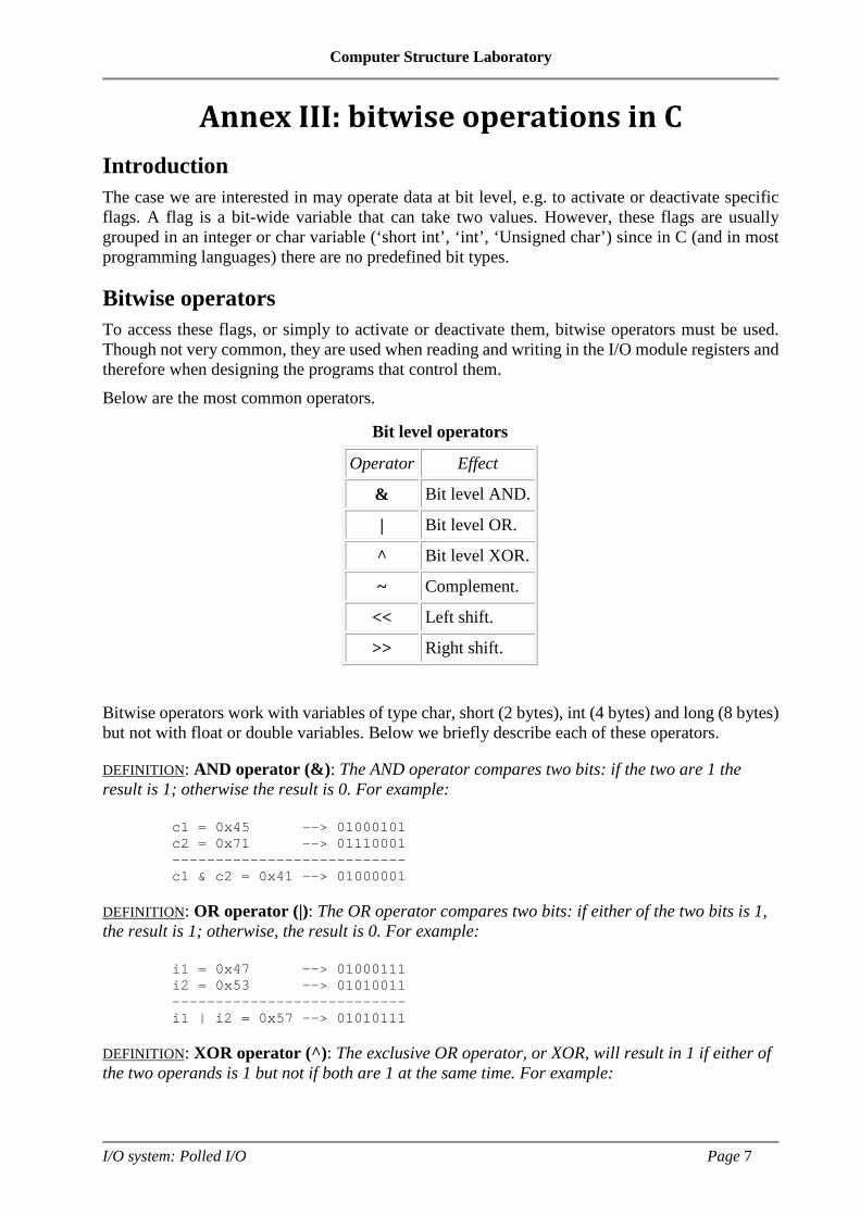
Elements in 0xBFA00000 (Module 2) Remember that in the 0xBFA00000 memory position there is an I/O module with the following elements connected:
1. Push button K2 2. Push button K1 3. Timer
These entries can be modified through the following window:
The status of each entry can be checked by reading 8 bits from the 0xBFA00000 position. Each bit has the following meaning:
- 0xBFA00000 Interrupts I/O (8-bit) - Bit: - 0 – K2 (Input) - 1 – K1 (Input) - 2 – Timer (Input) - 3 – N/A (not defined) - 4 – K2 latch - 5 – K1 latch - 6 – Timer latch

Computer Structure Laboratory
I/O system: Polled I/O Page 6
- 7 – N/A (not defined)
When a button is pressed or the external timer is activated, an interrupt request is made. This request is associated with external interrupt line 3 connected to the microprocessor. The event that caused the interrupt remains stored in the corresponding latch. The value of the latch is not deactivated until a specific write is made on the same position 0xBFA00000, setting the bit to zero. The three interrupt sources share the same microprocessor external interrupt line (line 3 of the IP6-2 interrupt lines). All three therefore produce the same hardware interrupt, which may or may not be enabled. To enable this interrupt through the interrupt mask of the Status register, we must set the 13th bit to 1, which corresponds to interrupt line IP5. Otherwise, the interrupt does not occur even though the bits of the status register of the 0xBFA00000 position are activated.
Computer Structure Laboratory
I/O system: Polled I/O Page 7
Annex III: bitwise operations in C Introduction The case we are interested in may operate data at bit level, e.g. to activate or deactivate specific flags. A flag is a bit-wide variable that can take two values. However, these flags are usually grouped in an integer or char variable (‘short int’, ‘int’, ‘Unsigned char’) since in C (and in most programming languages) there are no predefined bit types.
Bitwise operators To access these flags, or simply to activate or deactivate them, bitwise operators must be used. Though not very common, they are used when reading and writing in the I/O module registers and therefore when designing the programs that control them. Below are the most common operators. Bitwise operators work with variables of type char, short (2 bytes), int (4 bytes) and long (8 bytes) but not with float or double variables. Below we briefly describe each of these operators. DEFINITION: AND operator (&): The AND operator compares two bits: if the two are 1 the result is 1; otherwise the result is 0. For example: c1 = 0x45 --> 01000101 c2 = 0x71 --> 01110001 --------------------------- c1 & c2 = 0x41 --> 01000001 DEFINITION: OR operator (|): The OR operator compares two bits: if either of the two bits is 1, the result is 1; otherwise, the result is 0. For example: i1 = 0x47 --> 01000111 i2 = 0x53 --> 01010011 --------------------------- i1 | i2 = 0x57 --> 01010111 DEFINITION: XOR operator (^): The exclusive OR operator, or XOR, will result in 1 if either of the two operands is 1 but not if both are 1 at the same time. For example:
Bit level operators
Operator Effect
& Bit level AND.
| Bit level OR.
^ Bit level XOR.
~ Complement.
<< Left shift.
>> Right shift.
Computer Structure Laboratory
I/O system: Polled I/O Page 8
i1 = 0x47 --> 01000111 i2 = 0x53 --> 01010011 --------------------------- i1 ^ i2 = 0x14 --> 00010100 DEFINITION: Complement operator (~): This operator returns as a result the one’s complement of the operand: c = 0x45 --> 01000101 ---------------------- ~c = 0xBA --> 10111010 DEFINITION: Bit level shift operators (<< y >>): These operators shift a specified number of bits to the left or right. In a shift to the left, the remaining bits on the left side are discarded and the new spaces are filled with zeros. Shifts to the right work in the same way. For example:
c = 0x1C 00011100
c <<1 c = 0x38 00111000
c >>2 c = 0x07 00000111
Review the digital logic fundamentals and use of these operations in C/C ++, which we have seen in previous courses.
Computer Structure Laboratory
I/O system: Interrupts Page 1
Laboratory 5:
Input/Output System (II): Interrupts
(Updated at 29/01/2019) Work at home (planned) time: 1:30h
Lab time: 2:30h
1. Introduction In this laboratory session we will study the interrupts technique for synchronizing the computer with its peripheral devices.
Goals On completion of this session you will be able to - design algorithms to check or modify the value of the activation, status and mask bits of a processor’s interrupts system, - use C bitwise operators to check and modify the flags of the registers associated with an interrupt, and - implement programs written in C, using interrupts that control the input/output of the I/O modules of the MipsIT.
2. Preliminary (pre-lab) work All members of the workgroups should read Annex I, which describes the registers involved in the MIPS interrupts system, and Annex II, which presents two examples (one in assembly code and one in C language) of how the interrupts are managed. Students should also review all the concepts on the computer I/O system they have studied so far in their theoretical classes. After reading the annexes and the recommended bibliography, answer the following questions:
Q1. Briefly explain what an interrupt is. Q2. Briefly describe the interrupt sources of the MipsIt. Q3. How can we know what interrupt type or exception has been requested in the MipsIt
simulator? Q4. Indicate which bits should be activated in the Mipsit registers to enable the external
interrupt sources of the simulator (explained in Annex III). Q5. When executing the code of the C example program (Annex II), explain the values obtained
for the Cause and I/O registers (located in the 0xbfa00000 position). The interrupt handler shows these values after an interrupt from the K1 button.
Q6. Explain what is intended for the functions init_ext_int(), enable_int(EXT_INT3) and install_normal_int(InterruptHandler)
Lab 5
Computer Structure Laboratory
I/O system: Interrupts Page 2
of the C example program in Annex II. What effect do they have on the interrupts configuration registers?
Q7. Design (in pseudocode or using a flow diagram) an interrupts-based program that implements a cyclic counter using the external timer signal of the MipsIt module, i.e. whenever the timer produces a rising edge, the program increments an internal variable called counter whose content must be shown by the LEDs of the I/O module 1. The example of the C program in the annex should be used as a basis.
Q8. Explain which method – polling or interrupts – would be more suitable for managing the detection of buttons K1 and K2 of the Mipsit. Would this method be more suitable for the external timer? Would it influence the frequency of the timer?
First checkpoint: Answers to Q1-Q8 must be written up and handed in to your lecturer at the beginning of the session.
3. Lab (in-lab) workIn this session we will see the programming and management of the I/O modules in a practical way. To do so we will design several programs that involve the use of these modules. Bear in mind that the compiler's default options must be edited as in section 3.1 in P1 since we are accessing the processor’s I/O space. 3.1 The program proposed in pre-lab work point 7 must be implemented using the timer interrupts. 3.2 A second program, similar to first, that increases a counter using the timer interrupts, must also be implemented. For this second program, the K1 button must be used as an enable signal. In this way, the counter would be enabled only when K1 is active (high level), so its value will increase as the pulses of the timer increase. Conversely, if K1 is inactive, the counter’s value will not increase even if external timer pulses occur.
Second checkpoint: Show the proper functioning and codes of both programs to your lecturer.
We propose implementing a C program in the MipsIt simulation environment to control a traffic light system. This program should be implemented with the interrupts synchronization technique, so do not copy the code from the previous laboratory session. Assume that the traffic light system is made up of:
• 3 colours for the vehicle traffic lights: red, yellow and green
• 3 colours for the pedestrian traffic lights: red, yellow and greenTo simulate the switching on and off of the lights, we will use the LEDs in I/O module 1. We divide them into 2 banks of 4 LEDs and assume that the red lamps are the 2 most significant LEDs in each bank. The yellow and green lamps must form the rest of the LEDs, in the same order. The traffic light system must behave as follows:
• Initially the traffic light system always gives way to vehicles. The lights must therefore begreen for cars and red for pedestrians.

Computer Structure Laboratory
I/O system: Interrupts Page 3
• When a pedestrian presses the pedestrian crossing button (button K1 in module 2), the traffic light changes automatically, turning the traffic light for the vehicles to yellow.
• After a certain wait period, the light must change again (this time to red) and the vehicle pass light plus the pedestrian traffic light must both change to green.
• When the pedestrian crossing time has finished, the pedestrian traffic light must turn to yellow, while the vehicle traffic light remains on red. The system must then return to its initial state.
To set the time in each state, the external timer (located in module 2) must be used. The time in each case must be:
• The yellow light must be On for 5 pulses of the external timer for both vehicles and pedestrians.
• The red light for vehicles (green for pedestrians) must be On for 20 pulses of the external timer.
Bear in mind that the compiler’s default options must be edited as section 3.1 in P1 since we are accessing the processor’s I/O space. Third checkpoint: The traffic light program must be implemented using the interrupts synchronization method and simulated within the MipsIt program. Show the proper functioning of the program and the code to your lecturer.
Computer Structure Laboratory
I/O system: Interrupts Page 4
Annex I: Mips interrupts Introduction An exception/interrupt is any event that breaks a program’s normal execution sequence. We can differentiate between two types of events:
• exceptions, which occur when the event to be processed is caused by an error during the execution of an instruction (overflow, division by zero, etc.), and
• interrupts, which are microprocessor external events generated by an I/O device. This section describes the handling of interrupts within the MIPS architecture. In the MIPS microprocessor, besides the CPU, a series of coprocessors are integrated. Specifically, coprocessor 0 is responsible for managing the operation of exceptions and interrupts. The following registers belong to coprocessor 0:
• BadVAddr: This stores the memory address that caused the exception.
• Status: This stores the interrupt mask and authorization bits.
• Cause: This stores the exception type and pending interrupt bits.
• EPC: This stores the address of the instruction that was being executed when the exception/interrupt occurred.
Status register The status register bits control the exceptions/interrupt that can be activated. There is one bit for each of the 5 hardware interrupt lines and 3 for the defined software interrupts. The Interrupt mask contains one bit for each of the five external interrupt inputs. Bit 10 corresponds to the external interrupt request input 0, bit 11 corresponds to input 1, bit 12 corresponds to input 2, bit 13 corresponds to input 3, and bit 14 corresponds to input 4:
• Bit 10 => Input 0.
• Bit 11 => Input 1.
• Bit 12 => Input 2.
• Bit 13 => Input 3. • Bit 14 => Input 4.
If the enable bit is set to 1, the interrupt is enabled. On the other hand, if the enable bit is set to 0, the interrupt is disabled. The lowest bit in the Status register acts as a global enabling bit for all interrupts. Thus, the least significant bit (Bit 0) is the interrupt permission bit. If this is set to 1 the interrupts are enabled and if it is set to 0 they are all masked. The kernel/user bit is an information bit. If it is set to 0, the program was in the kernel mode of the operating system when the exception occurred. Conversely, if the Kernel/User bit is set to 1, the program was in user mode. Whenever an exception/interrupt occurs, these 6 bits move two positions to the left. The previous bits become the old ones, the current ones become the previous ones, and current ones are set to 0.
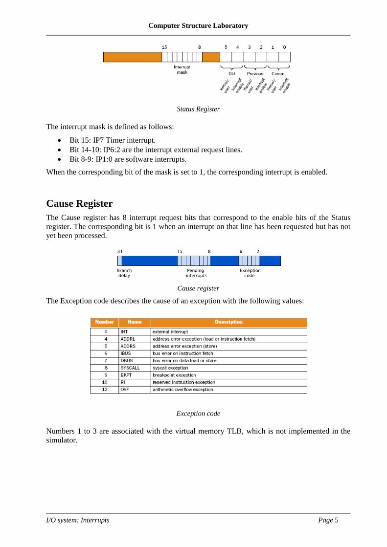
Computer Structure Laboratory
I/O system: Interrupts Page 5
Status Register
The interrupt mask is defined as follows:
• Bit 15: IP7 Timer interrupt. • Bit 14-10: IP6:2 are the interrupt external request lines. • Bit 8-9: IP1:0 are software interrupts.
When the corresponding bit of the mask is set to 1, the corresponding interrupt is enabled.
Cause Register The Cause register has 8 interrupt request bits that correspond to the enable bits of the Status register. The corresponding bit is 1 when an interrupt on that line has been requested but has not yet been processed.
Cause register
The Exception code describes the cause of an exception with the following values:
Exception code
Numbers 1 to 3 are associated with the virtual memory TLB, which is not implemented in the simulator.
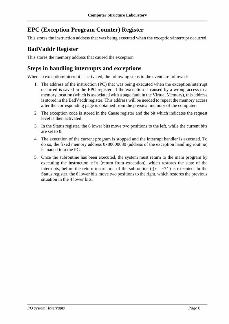
Computer Structure Laboratory
I/O system: Interrupts Page 6
EPC (Exception Program Counter) Register This stores the instruction address that was being executed when the exception/interrupt occurred.
BadVaddr Register This stores the memory address that caused the exception.
Steps in handling interrupts and exceptions When an exception/interrupt is activated, the following steps to the event are followed:
1. The address of the instruction (PC) that was being executed when the exception/interrupt occurred is saved in the EPC register. If the exception is caused by a wrong access to a memory location (which is associated with a page fault in the Virtual Memory), this address is stored in the BadVaddr register. This address will be needed to repeat the memory access after the corresponding page is obtained from the physical memory of the computer.
2. The exception code is stored in the Cause register and the bit which indicates the request level is then activated.
3. In the Status register, the 6 lower bits move two positions to the left, while the current bits are set to 0.
4. The execution of the current program is stopped and the interrupt handler is executed. To do so, the fixed memory address 0x80000080 (address of the exception handling routine) is loaded into the PC.
5. Once the subroutine has been executed, the system must return to the main program by executing the instruction rfe (return from exception), which restores the state of the interrupts, before the return instruction of the subroutine (jr r31) is executed. In the Status register, the 6 lower bits move two positions to the right, which restores the previous situation in the 4 lower bits.
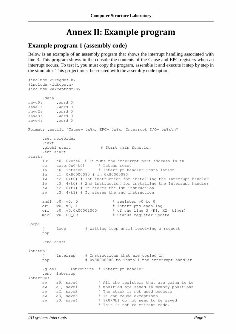
Computer Structure Laboratory
I/O system: Interrupts Page 7
Annex II: Example program Example program 1 (assembly code) Below is an example of an assembly program that shows the interrupt handling associated with line 3. This program shows in the console the contents of the Cause and EPC registers when an interrupt occurs. To test it, you must copy the program, assemble it and execute it step by step in the simulator. This project must be created with the assembly code option. #include <iregdef.h> #include <idtcpu.h> #include <excepthdr.h> .data save0: .word 0 save1: .word 0 save2: .word 0 save3: .word 0 save4: .word 0 Format: .asciiz "Cause= 0x%x, EPC= 0x%x, Interrupt I/O= 0x%x\n" .set noreorder .text .globl start # Start main function .ent start start: lui t0, 0xbfa0 # It puts the interrupt port address in t0 sb zero,0x0(t0) # Latchs reset la t0, intstub # Interrupt handler installation la t1, 0x80000080 # in 0x80000080 lw t2, 0(t0) # 1st instruction for installing the Interrupt handler lw t3, 4(t0) # 2nd instruction for installing the Interrupt handler sw t2, 0(t1) # It stores the 1st instruction sw t3, 4(t1) # It stores the 2nd instruction andi v0, v0, 0 # register v0 to 0 ori v0, v0, 1 # interrupts enabling ori v0, v0,0x00002000 # of the line 3 (K1, K2, timer) mtc0 v0, C0_SR # Status register update Loop: j Loop # waiting loop until receiving a request nop .end start intstub: j interrup # Instructions that are copied in nop # 0x80000080 to install the interrupt handler .globl introutine # interrupt handler .ent interrup interrup: sw a0, save0 # All the registers that are going to be sw a1, save1 # modified are saved in memory positions sw a2, save2 # The stack is not used because sw a3, save3 # it can cause exceptions. sw s0, save4 # $k0/$k1 do not need to be saved # This is not re-entrant code.
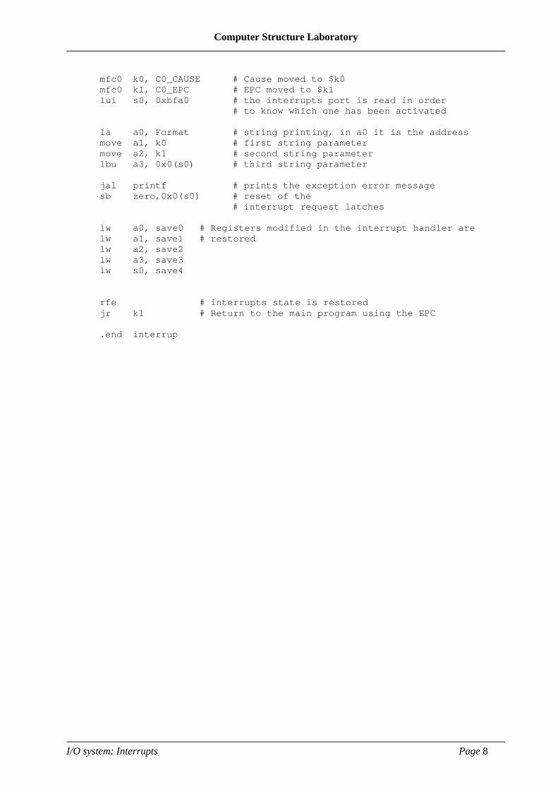
Computer Structure Laboratory
I/O system: Interrupts Page 8
mfc0 k0, C0_CAUSE # Cause moved to $k0 mfc0 k1, C0_EPC # EPC moved to $k1 lui s0, 0xbfa0 # the interrupts port is read in order # to know which one has been activated la a0, Format # string printing, in a0 it is the address move a1, k0 # first string parameter move a2, k1 # second string parameter lbu a3, 0x0(s0) # third string parameter jal printf # prints the exception error message sb zero,0x0(s0) # reset of the # interrupt request latches lw a0, save0 # Registers modified in the interrupt handler are lw a1, save1 # restored lw a2, save2 lw a3, save3 lw s0, save4 rfe # interrupts state is restored jr k1 # Return to the main program using the EPC .end interrup
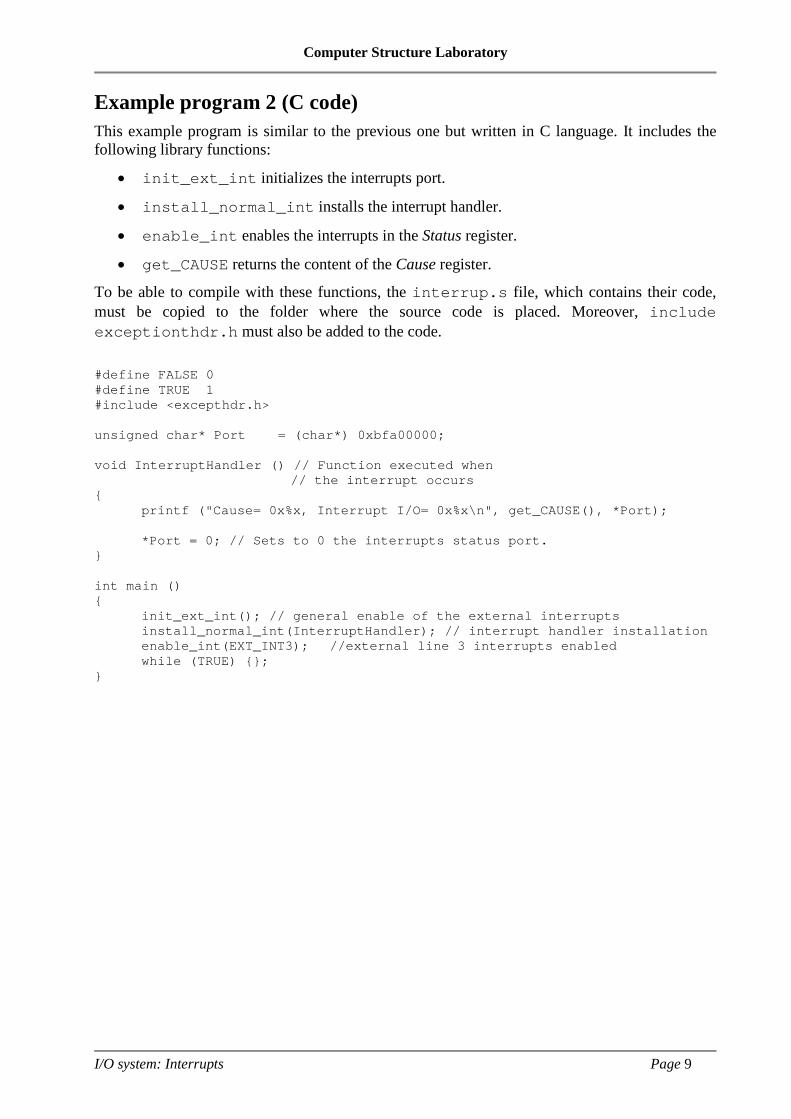
Computer Structure Laboratory
I/O system: Interrupts Page 9
Example program 2 (C code) This example program is similar to the previous one but written in C language. It includes the following library functions:
• init_ext_int initializes the interrupts port.
• install_normal_int installs the interrupt handler.
• enable_int enables the interrupts in the Status register.
• get_CAUSE returns the content of the Cause register.
To be able to compile with these functions, the interrup.s file, which contains their code, must be copied to the folder where the source code is placed. Moreover, include exceptionthdr.h must also be added to the code.
#define FALSE 0 #define TRUE 1 #include <excepthdr.h> unsigned char* Port = (char*) 0xbfa00000; void InterruptHandler () // Function executed when // the interrupt occurs { printf ("Cause= 0x%x, Interrupt I/O= 0x%x\n", get_CAUSE(), *Port); *Port = 0; // Sets to 0 the interrupts status port. } int main () { init_ext_int(); // general enable of the external interrupts install_normal_int(InterruptHandler); // interrupt handler installation enable_int(EXT_INT3); //external line 3 interrupts enabled while (TRUE) {}; }
Computer Structure Laboratory
I/O system: Interrupts Page 10
Annex III: MipsIt I/O memory space (reminder)
Introduction The input/output (I/O) system of a computer consists of the elements (buses, registers, protocols, etc.) that enable us to connect the computer to the peripheral devices. An I/O operation can be divided into three phases:
1. Addressing: Access to the module through its memory address. 2. Synchronization and control of the transfer: The mechanism used to determine whether
the peripheral is ready to begin a transfer (to send or to receive) data, control the transfer and control whether another transfer can be started.
3. Data transfer: Transfer of the data itself, which may require transforming data sent by the peripherals.
Synchronization is a critical stage in I/O operations and fundamental for correct data transfer. It also greatly influences the system’s final performance. Three commonly used techniques exist: polling (software-driven I/O), interrupts and direct memory transfer (DMA).
Interrupt-based or software-driven synchronization In the data transfer between the computer and the Input/Output (I/O) module, the CPU is responsible for transferring the memory data and sending them to the I/O module (in a write), or similarly, for storing the data from the I/O module in the memory (in a read). The arrival of data from outside the computer is normally unpredictable and the program cannot know exactly when an I/O module will have available data that must be read. A method is therefore needed to synchronize the execution of the program in the CPU with the I/O modules. Through this synchronization, the I/O module notifies the CPU when data are waiting to be read or when the queue of data to be written is empty.
Interrupt-based synchronization Through an interrupt request performed by the interrupt module, the I/O module notifies the CPU that there are data to transfer. However, the CPU is responsible for extracting the data from the module (in the case of reading) or for sending the data to the module (in case of writing).
Polling (Software-driven) synchronization With this method the CPU executes a program that directly controls the I/O transfer. The program is responsible for sending the order and waits until the data transfer is complete. The program continuously checks the I/O module status until the transfer is complete. The polling is commonly implemented via a loop that does not end until all the data are transferred. As in the previous case, therefore, each of the transferred data passes through the CPU.
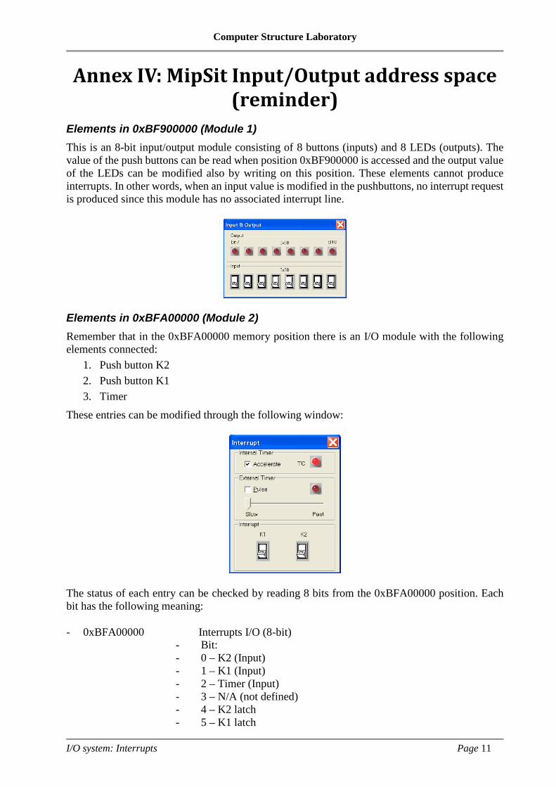
Computer Structure Laboratory
I/O system: Interrupts Page 11
Annex IV: MipSit Input/Output address space (reminder)
Elements in 0xBF900000 (Module 1) This is an 8-bit input/output module consisting of 8 buttons (inputs) and 8 LEDs (outputs). The value of the push buttons can be read when position 0xBF900000 is accessed and the output value of the LEDs can be modified also by writing on this position. These elements cannot produce interrupts. In other words, when an input value is modified in the pushbuttons, no interrupt request is produced since this module has no associated interrupt line.
Elements in 0xBFA00000 (Module 2) Remember that in the 0xBFA00000 memory position there is an I/O module with the following elements connected:
1. Push button K2 2. Push button K1 3. Timer
These entries can be modified through the following window:
The status of each entry can be checked by reading 8 bits from the 0xBFA00000 position. Each bit has the following meaning:
- 0xBFA00000 Interrupts I/O (8-bit) - Bit: - 0 – K2 (Input) - 1 – K1 (Input) - 2 – Timer (Input) - 3 – N/A (not defined) - 4 – K2 latch - 5 – K1 latch
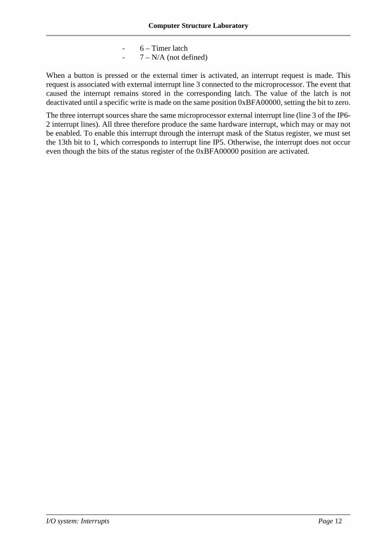
Computer Structure Laboratory
I/O system: Interrupts Page 12
- 6 – Timer latch - 7 – N/A (not defined)
When a button is pressed or the external timer is activated, an interrupt request is made. This request is associated with external interrupt line 3 connected to the microprocessor. The event that caused the interrupt remains stored in the corresponding latch. The value of the latch is not deactivated until a specific write is made on the same position 0xBFA00000, setting the bit to zero. The three interrupt sources share the same microprocessor external interrupt line (line 3 of the IP6-2 interrupt lines). All three therefore produce the same hardware interrupt, which may or may not be enabled. To enable this interrupt through the interrupt mask of the Status register, we must set the 13th bit to 1, which corresponds to interrupt line IP5. Otherwise, the interrupt does not occur even though the bits of the status register of the 0xBFA00000 position are activated.
Computer Structure Laboratory
Peripherals: Keyboard Page 1
Laboratory 6: Peripherals:
Keyboard (Updated at 29/01/2019)
Work at home (planned) time: 1:30h Lab time: 2:30h
1. Introduction In this laboratory session we will study how a computer keyboard works, explain low-level access to the I/O module that controls its functioning, and analyse how keyboard configuration commands are sent. To do so, we will study and modify several C programs in Linux.
Goals On completion of this practice session you will be able to - understand the configuration of a PC keyboard, - understand the structure and internal registers of a keyboard controller, especially the Intel 8742, - use the keyboard configuration commands available in the hardware of the keyboard and the PC I/O module, - use low-level C input/output functions of the Linux operating system to check and modify the register bits integrated into the keyboard controller, and - design and implement C programs that change the keyboard configuration and read the Scan codes of the keys pressed by the user.
Resources These laboratory sessions will be carried out using a PC and a virtual machine with the Linux operating system (Ubuntu). To run the virtual machine, you need to have installed the VMware player software, which is free and can be downloaded from the VMware company website. The Linux virtual machine files are available from the Virtual Classroom. Once the file has been decompressed, it can be executed in the virtual machine player (see Annex III). The Linux virtual machine has had pre-installed all the software needed to compile and execute the programs to be implemented during the laboratory session.
2. Preliminary (pre-lab) work You must complete the following activities to get the most out of this laboratory session. It is important that you spend the indicated amount of time on them. All members of the workgroup should read annexes I, II and III of this document. These explain the hardware configuration of the keyboard controller, illustrate a program that uses the I/O functions needed to implement this kind of program, and describe how the Linux virtual machine is used to compile and execute programs. After reading the annexes, answer the following questions: Q1. Which address/port is used to receive data from the keyboard?
Lab 6
Computer Structure Laboratory
Peripherals: Keyboard Page 2
Q2. How can you know that there are data from the keyboard ready to be read? Q3. Through which address/port are the commands sent to the keyboard? Q4. What is the Scan code associated with a key and the Make and Break codes?
Q5. What are the iopl, outb and inb functions for?
Q6. What does the code in Annex II do? Provide a reasoned answer. Q7. Which kind of synchronization technique (polling or interrupts) has been used in the
program in Annex II to determine when data from the keyboard are available in the controller?
First checkpoint: Answers to Q1-Q7 must be written up and handed in to your lecturer at the beginning of the session.
3. Lab (in-lab) workIn this session we will study the programming and management of the keyboard in the Linux operating system in a practical way by designing several programs that use this peripheral. 3.1 Compile and execute the program in Annex II. To do so, save the code in a file with a ".c" extension. The program can be compiled and executed from the command line of a terminal of the virtual machine (see Annex III). The functioning of the program and the values returned by the keyboard must be checked. 3.2 Implement a C program that changes the state of the LEDS of the keyboard. The program should first turn on the three LEDs, then wait for a second, turn them off, and then wait for another second. The program must repeat this blinking 5 times. See the schematic of the program in the previous section for a hint on how to do this. 3.3 Implement a third program that deactivates the keyboard for 10 seconds and reactivates it after waiting 10 seconds. The program must be written using the commands explained at the end of Annex I. The keyboard must not respond even if a key is pressed. For this, you need to edit, compile and execute the program as in the previous example.
Second checkpoint: Show the proper functioning of the programs to the lecturer. Answer any questions on their design and operation.
3.4 Implement a fourth C program using the knowledge acquired from the previous ones. This fourth program must continuously read the scan codes of the pressed keys and display them on screen in hexadecimal format. Synchronization with the keyboard must be done by polling, i.e. by continuously checking whether data are available and accessing them as soon as they are detected. This checking process must be repeated indefinitely until a particular key is detected (for example, the "q" key, whose associated Make code is 0x10). Pressing this key should end the reading loop and terminate the program. To avoid interference with the characters shown by the terminal, the terminal character echo should be deactivated. The code that should be added at the beginning and end of the program to avoid terminal echo is:
Computer Structure Laboratory
Peripherals: Keyboard Page 3
// The following directives have to be included for the libraries that contain the / / functions that will be used below #include <unistd.h> #include <termios.h> // the following two variables have to be declared to read and store the current // terminal configuration state struct termios attr; struct termios orig_attr; // the tcgetattr function reads the keyboard treatment attributes in the terminal tcgetattr(STDIN_FILENO, &orig_attr); attr = orig_attr; // we deactivate the flag that produces echo attr.c_lflag &= ~(ECHO) ; // the tcsetattr function writes the new attributes tcsetattr(STDIN_FILENO, TCSAFLUSH, &attr);
Before the program ends, the original configuration must be restored. To do so, add the following code: // these functions are to empty the keyboard buffer of possible characters that // are waiting to be read since we have deactivated the echo previously where // chac is a variable of type: unsigned char chac [256]; printf("\r\n To finish the program, press any key + enter\r\n"); scanf("%s",chac); // This function retrieves the original attributes of the terminal tcsetattr(STDIN_FILENO, TCIFLUSH, &orig_attr);
After you have checked the operation of program 3.4, answer these questions:
3.4.1 Write the Make and Break codes for the following keys: a, k, Alt and Enter.
3.4.2 What happens when you hold down a key for a long time? 3.4.3 What happens when the program is running and at the same time the mouse is moved?
Third checkpoint: Show the proper functioning of the programs to the lecturer. Answer any questions on their design and operation.
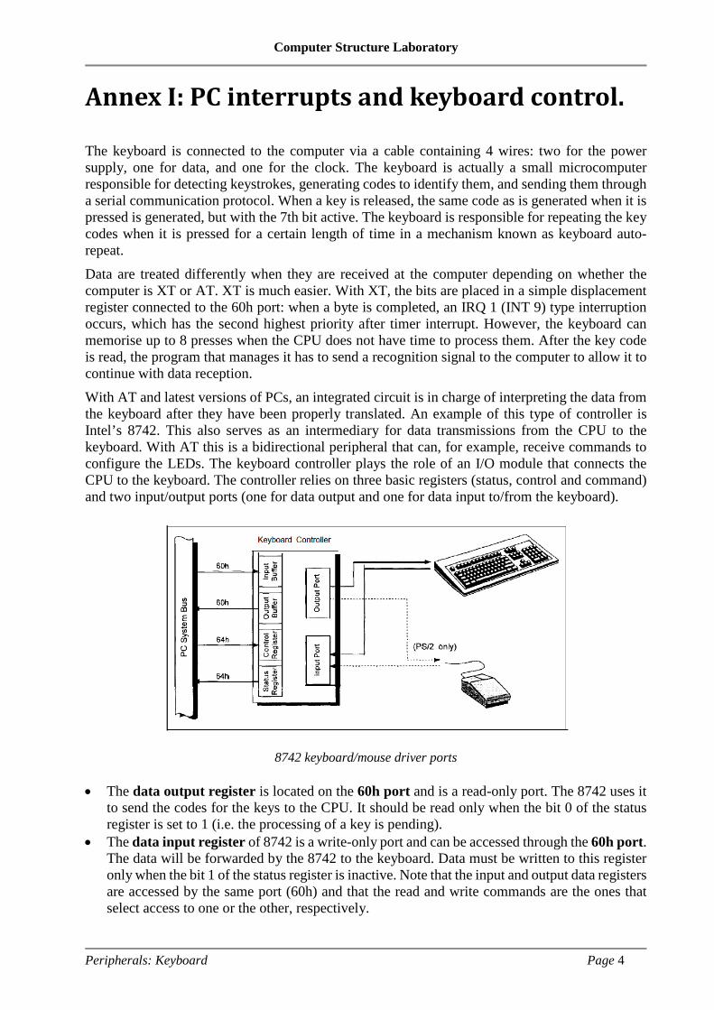
Computer Structure Laboratory
Peripherals: Keyboard Page 4
Annex I: PC interrupts and keyboard control. The keyboard is connected to the computer via a cable containing 4 wires: two for the power supply, one for data, and one for the clock. The keyboard is actually a small microcomputer responsible for detecting keystrokes, generating codes to identify them, and sending them through a serial communication protocol. When a key is released, the same code as is generated when it is pressed is generated, but with the 7th bit active. The keyboard is responsible for repeating the key codes when it is pressed for a certain length of time in a mechanism known as keyboard auto-repeat. Data are treated differently when they are received at the computer depending on whether the computer is XT or AT. XT is much easier. With XT, the bits are placed in a simple displacement register connected to the 60h port: when a byte is completed, an IRQ 1 (INT 9) type interruption occurs, which has the second highest priority after timer interrupt. However, the keyboard can memorise up to 8 presses when the CPU does not have time to process them. After the key code is read, the program that manages it has to send a recognition signal to the computer to allow it to continue with data reception. With AT and latest versions of PCs, an integrated circuit is in charge of interpreting the data from the keyboard after they have been properly translated. An example of this type of controller is Intel’s 8742. This also serves as an intermediary for data transmissions from the CPU to the keyboard. With AT this is a bidirectional peripheral that can, for example, receive commands to configure the LEDs. The keyboard controller plays the role of an I/O module that connects the CPU to the keyboard. The controller relies on three basic registers (status, control and command) and two input/output ports (one for data output and one for data input to/from the keyboard).
8742 keyboard/mouse driver ports
• The data output register is located on the 60h port and is a read-only port. The 8742 uses it to send the codes for the keys to the CPU. It should be read only when the bit 0 of the status register is set to 1 (i.e. the processing of a key is pending).
• The data input register of 8742 is a write-only port and can be accessed through the 60h port. The data will be forwarded by the 8742 to the keyboard. Data must be written to this register only when the bit 1 of the status register is inactive. Note that the input and output data registers are accessed by the same port (60h) and that the read and write commands are the ones that select access to one or the other, respectively.
Computer Structure Laboratory
Peripherals: Keyboard Page 5
• The status register can be accessed by reading from the 64h I/O port and read at any time. The meaning of the bits is as follows: o Bit 0. Data output port full. 1 indicates that the 8742 has placed a datum in the output port
(60h port) and the CPU has not read it yet. This bit is set to 0 when the CPU reads the 60h port.
o Bit 1. Data input port full. 1 means that a datum has been placed in the input port (60h port) and the 8742 has not read it yet.
o Bit 2. Auto-test successful. This is 1 if the test was successful and 0 otherwise or after booting.
o Bit 3. Command/data. This is set to 1 or 0 when something is sent to the 60h or 64h port, respectively. In this way, the 8742 knows whether what is sent are commands or data (commands = 1).
o Bit 4. Inhibition bit. This bit is updated whenever a datum is placed in the data output port (60h port).
o Bit 5. Out of time transmission. This indicates that the transmission of data to the keyboard has not been answered in the appropriate timeframe.
o Bit 6. Out of time reception. This indicates that the keyboard has not sent data within the appropriate timeframe.
o Bit 7. Parity error. This indicates the parity of the received data: 0 is the correct value.
Commands accepted by the keyboard The keyboard accepts several commands. These commands can be sent to the keyboard at any time through the 60h port of the 8742 keyboard controller and will be redirected to the keyboard. The keyboard must respond in under 20 milliseconds, returning a recognition signal via a 0FAh byte. The main commands (differentiated from the data by an active 7th bit) are:
• Reset (0FFh): This command performs a keyboard reset and a self-test. As a result, the keyboard answers with: 0xAA (self-test passed), 0xFC or 0xFD (self-test failed).
• Forwarding (0FEh): The system can send this command to the keyboard when it detects a keyboard reception failure. This command can only be sent after a keyboard transmission and before enabling the communication for the next reception. The keyboard responds by re-sending the previous data.
• Set default values (0F6h): This returns the auto-repetition to the default value, cleans its output register and continues reading keys if it is not inhibited. It is a kind of hot reset.
• Disable (0F5h): This is the same as the previous command but does not read the keys and remains inhibited until further instructions.
• Enable (0F4): This resumes an operation that has been interrupted by the previous or any other command.
• Set ratio and auto-repetition delay (0F3h): After this command, another one must be sent immediately. This will be interpreted as data, establishing the values of auto-repetition. In this second byte, bit 7 will always be zero while the other bits indicate speed. Value 1Fh sets the repetition factor to the minimum possible, while 00h sets it to the maximum possible.
Computer Structure Laboratory
Peripherals: Keyboard Page 6
• Set/identify scan codes (0F0h): This command selects one of the three alternative scan code sets on the MF II keyboard. Values 1, 2 or 3 are valid. The standard configuration is scan codes set to 2. After the command, the keyboard responds with an ACK code (value 0xFA) and waits for the transfer of the second byte with the selected scan code repertoire. Option: 1, 2 or 3.
• No operation (0F7h to 0FDh and 0EFh to 0F2h): These are reserved codes. When receiving them, the keyboard sends a recognition signal and performs no action.
• Echo (0EEh): If the keyboard receives this command, it replies by sending it to the PC. This is a way of helping in the device diagnosis.
• Turn LEDs on/off (0EDh). After this command is sent, another data byte must be sent whose bits 0, 1 and 2 are linked to the state of the Scroll Lock, Num Lock and Caps Lock LEDs, respectively. The other bits are reserved.
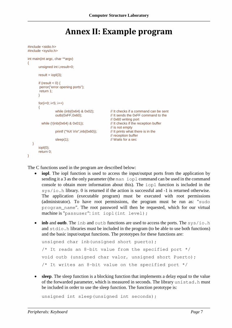
Computer Structure Laboratory
Peripherals: Keyboard Page 7
Annex II: Example program #include <stdio.h> #include <sys/io.h> int main(int argc, char **argv) { unsigned int i,result=0; result = iopl(3); if (result < 0) { perror("error opening ports"); return 1; } for(i=0; i<5; i++) { while (inb(0x64) & 0x02); // It checks if a command can be sent outb(0xFF,0x60); // It sends the 0xFF command to the // 0x60 writing port while (!(inb(0x64) & 0x01)); // It checks if the reception buffer // is not empty printf ("%X \r\n",inb(0x60)); // It prints what there is in the // reception buffer sleep(1); // Waits for a sec } iopl(0); return 0; }
The C functions used in the program are described below: • iopl. The iopl function is used to access the input/output ports from the application by
sending it a 3 as the only parameter (the man iopl command can be used in the command console to obtain more information about this). The iopl function is included in the sys/io.h library. 0 is returned if the action is successful and -1 is returned otherwise. The application (executable program) must be executed with root permissions (administrator). To have root permissions, the program must be run as: "sudo program_name". The root password will then be requested, which for our virtual machine is "passuser": int iopl(int level);
• inb and outb. The inb and outb functions are used to access the ports. The sys/io.h and stdio.h libraries must be included in the program (to be able to use both functions) and the basic input/output functions. The prototypes for these functions are: unsigned char inb(unsigned short puerto);
/* It reads an 8-bit value from the specified port */
void outb (unsigned char valor, unsigned short Puerto);
/* It writes an 8-bit value on the specified port */
• sleep. The sleep function is a blocking function that implements a delay equal to the value of the forwarded parameter, which is measured in seconds. The library unistad.h must be included in order to use the sleep function. The function prototype is: unsigned int sleep(unsigned int seconds);
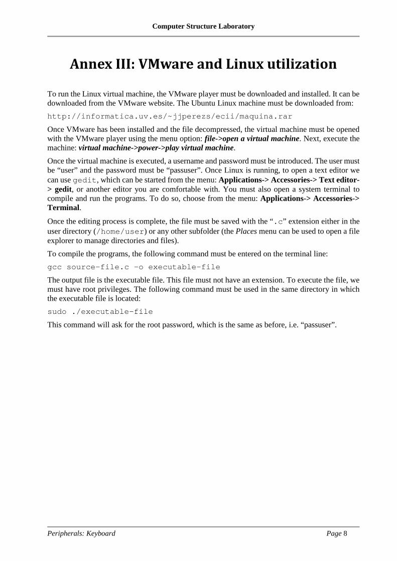
Computer Structure Laboratory
Peripherals: Keyboard Page 8
Annex III: VMware and Linux utilization To run the Linux virtual machine, the VMware player must be downloaded and installed. It can be downloaded from the VMware website. The Ubuntu Linux machine must be downloaded from: http://informatica.uv.es/~jjperezs/ecii/maquina.rar
Once VMware has been installed and the file decompressed, the virtual machine must be opened with the VMware player using the menu option: file->open a virtual machine. Next, execute the machine: virtual machine->power->play virtual machine. Once the virtual machine is executed, a username and password must be introduced. The user must be “user” and the password must be “passuser”. Once Linux is running, to open a text editor we can use gedit, which can be started from the menu: Applications-> Accessories-> Text editor-> gedit, or another editor you are comfortable with. You must also open a system terminal to compile and run the programs. To do so, choose from the menu: Applications-> Accessories-> Terminal.
Once the editing process is complete, the file must be saved with the “.c” extension either in the user directory (/home/user) or any other subfolder (the Places menu can be used to open a file explorer to manage directories and files). To compile the programs, the following command must be entered on the terminal line: gcc source-file.c –o executable-file
The output file is the executable file. This file must not have an extension. To execute the file, we must have root privileges. The following command must be used in the same directory in which the executable file is located: sudo ./executable-file
This command will ask for the root password, which is the same as before, i.e. “passuser”.
Computer Structure Laboratory
Peripherals: Magnetic disc Page 1
Laboratory 7: Peripherals:
Magnetic disc (Updated at 29/01/2019)
Work at home (planned) time: 1:30h Lab time: 2:30h
1. Introduction In this laboratory session we will study how computer magnetic drives work. We will describe how commands are sent to the disk and explain how to control I/O-related modules with low-level commands. We will also implement several programs in C to exemplify how to control the magnetic disc in Linux.
Goals On completion of this laboratory session you will be able to
- understand the structure of the magnetic disk and how information is accessed from it, - understand the structure and internal registers of the IDE disk interface, - use the basic commands for disk configuration that are available in the PC I/O modules, - use low-level C input/output functions in the Linux operating system to check and modify
the bits of the registers integrated into the disk controllers, and - design and implement low-level C programs to access the disk information.
Resources VMware player and the same Ubuntu Linux machine as in the previous laboratory session.
2. Preliminary (pre-lab) work You must complete the following activities to get the most out of this laboratory session. It is important that you spend the indicated amount of time on them. All members of the workgroup should read annexes I, II and III of this document. These annexes explain the hardware configuration of the disc controller, describe the partition table structure, and provide an example program. You should also review all the related concepts explained in the theoretical class. After reading the annexes, answer the following questions:
Q1. What is the CHS (cylinder, head, sector) addressing format? Q2. What is the LBA (linear block allocation) addressing format? Q3. Read the program in Annex III and explain how it functions. Q4. What is the word width of the data exchanged with the disk? Q5. On which register of the IDE interface is the command to be completed by the disk written? Q6. What command is used in the program in Annex III? What is this command for?
Lab 7
Computer Structure Laboratory
Peripherals: Magnetic disc Page 2
Q7. How can you know that there are data in the disc ready to be read? Q8. For the program in Annex III, identify what kind of synchronization (polling or interrupts)
has been used to determine whether the disk has sent data.
First checkpoint: Answers to Q1-Q8 must be written up and handed in to your lecturer at the beginning of the session.
3. Lab (in-lab) workIn this session we will study magnetic disk programming and management in the Linux operating system in a practical way by implementing several programs that show the capabilities of this peripheral.
3.1 Compile the program in Annex III in a shell of the virtual machine, as explained in the previous laboratory session. Check the proper functioning of the code and the values returned by the disk before doing the following:
3.1.1 Identify the number of LBA sectors that can be addressed. To do so, look at the information bytes provided by the program in the 120 to 123 range, which correspond to words 60 and 61, as described in the identification information table on page 6 (remember that data are stored with Little-Endian sorting).
3.1.2 Execute the following command on the command line of a terminal in the virtual machine: sudo hdparm -g /dev/sdb. What number of sectors is obtained? Is there any coincidence with the values obtained in the previous question?
3.2 It must be implemented in C a program that reads sector 0 (Master Boot Record) and displays this MBR on the screen. The sector is stored with LBA format addressing in the slave IDE disk (in our Linux distribution this unit matches /dev/sdb). The bytes that are part of each partition table must be identified. Remember that the identifier of the unit to be passed to the controller at address 0x1F6 is 0xF0. Use the program in Annex III as a guide.
Execute the program before answering the following questions: 3.2.1 How many partitions are there in the partition table? Are any of them a booting
partition? 3.2.2 Identify the partition type (check the web for this, e.g.
http://en.wikipedia.org/wiki/Partition_type). 3.2.3 Identify, in LBA format, the starting sectors of the partitions and their size. 3.2.4 Do the previous data match those obtained by the command:
“sudo parted /dev/sdb unit s print”?
3.2.5 Repeat the experiment of reading a sector but this time reading sector 0 of the master disc, i.e. /dev/sda. What are these results for /dev/sda?
3.2.6 Check whether they are consistent with the result of the command “sudo fdisk –l”.

Computer Structure Laboratory
Peripherals: Magnetic disc Page 3
Second checkpoint: Show the proper functioning of the programs to the lecturer. Answer the prior questions and any other subject-related questions.
3.3 Implement a third C program that copies the Master Boot Record (sector 0 with LBA addressing of the slave IDE disk, which in our Linux distribution is identified as /dev/sdb), to sector 0 of the master IDE disk (which in our distribution is identified as /dev/sda). Be careful when copying because if the copy is made in the wrong direction, the virtual machine will be unusable. The copy must always be made from /dev/sdb (0xF0 identifier when writing in the 0x1F6 address) to /dev/sda (0xE0 identifier when writing in the 0x1F6 address).
3.3.1 Read section 0 of the disk /dev/sda again with the program from the previous section. Do the data provided by the disk /dev/sda match the data previously obtained? What is the difference?
Third checkpoint: Show the proper functioning of the programs to the lecturer. Answer any questions on their design and operation.
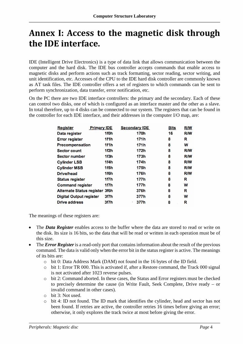
Computer Structure Laboratory
Peripherals: Magnetic disc Page 4
Annex I: Access to the magnetic disk through the IDE interface. IDE (Intelligent Drive Electronics) is a type of data link that allows communication between the computer and the hard disk. The IDE bus controller accepts commands that enable access to magnetic disks and perform actions such as track formatting, sector reading, sector writing, and unit identification, etc. Accesses of the CPU to the IDE hard disk controller are commonly known as AT task files. The IDE controller offers a set of registers to which commands can be sent to perform synchronization, data transfer, error notification, etc. On the PC there are two IDE interface controllers: the primary and the secondary. Each of these can control two disks, one of which is configured as an interface master and the other as a slave. In total therefore, up to 4 disks can be connected to our system. The registers that can be found in the controller for each IDE interface, and their addresses in the computer I/O map, are:
The meanings of these registers are: • The Data Register enables access to the buffer where the data are stored to read or write on
the disk. Its size is 16 bits, so the data that will be read or written in each operation must be of this size.
• The Error Register is a read-only port that contains information about the result of the previous command. The data is valid only when the error bit in the status register is active. The meanings of its bits are:
o bit 0: Data Address Mark (DAM) not found in the 16 bytes of the ID field. o bit 1: Error TR 000. This is activated if, after a Restore command, the Track 000 signal
is not activated after 1023 reverse pulses. o bit 2: Command aborted. In these cases, the Status and Error registers must be checked
to precisely determine the cause (in Write Fault, Seek Complete, Drive ready – or invalid command in other cases).
o bit 3: Not used. o bit 4: ID not found. The ID mark that identifies the cylinder, head and sector has not
been found. If retries are active, the controller retries 16 times before giving an error; otherwise, it only explores the track twice at most before giving the error.
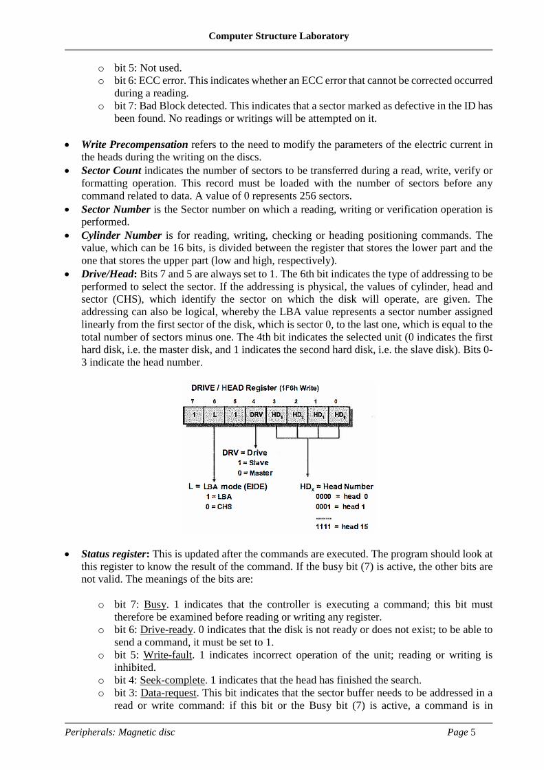
Computer Structure Laboratory
Peripherals: Magnetic disc Page 5
o bit 5: Not used. o bit 6: ECC error. This indicates whether an ECC error that cannot be corrected occurred
during a reading. o bit 7: Bad Block detected. This indicates that a sector marked as defective in the ID has
been found. No readings or writings will be attempted on it.
• Write Precompensation refers to the need to modify the parameters of the electric current in the heads during the writing on the discs.
• Sector Count indicates the number of sectors to be transferred during a read, write, verify or formatting operation. This record must be loaded with the number of sectors before any command related to data. A value of 0 represents 256 sectors.
• Sector Number is the Sector number on which a reading, writing or verification operation is performed.
• Cylinder Number is for reading, writing, checking or heading positioning commands. The value, which can be 16 bits, is divided between the register that stores the lower part and the one that stores the upper part (low and high, respectively).
• Drive/Head: Bits 7 and 5 are always set to 1. The 6th bit indicates the type of addressing to be performed to select the sector. If the addressing is physical, the values of cylinder, head and sector (CHS), which identify the sector on which the disk will operate, are given. The addressing can also be logical, whereby the LBA value represents a sector number assigned linearly from the first sector of the disk, which is sector 0, to the last one, which is equal to the total number of sectors minus one. The 4th bit indicates the selected unit (0 indicates the first hard disk, i.e. the master disk, and 1 indicates the second hard disk, i.e. the slave disk). Bits 0-3 indicate the head number.
• Status register: This is updated after the commands are executed. The program should look at this register to know the result of the command. If the busy bit (7) is active, the other bits are not valid. The meanings of the bits are:
o bit 7: Busy. 1 indicates that the controller is executing a command; this bit must therefore be examined before reading or writing any register.
o bit 6: Drive-ready. 0 indicates that the disk is not ready or does not exist; to be able to send a command, it must be set to 1.
o bit 5: Write-fault. 1 indicates incorrect operation of the unit; reading or writing is inhibited.
o bit 4: Seek-complete. 1 indicates that the head has finished the search. o bit 3: Data-request. This bit indicates that the sector buffer needs to be addressed in a
read or write command: if this bit or the Busy bit (7) is active, a command is in
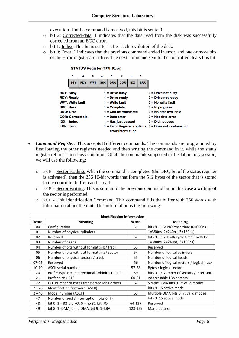
Computer Structure Laboratory
Peripherals: Magnetic disc Page 6
execution. Until a command is received, this bit is set to 0. o bit 2: Corrected-data. 1 indicates that the data read from the disk was successfully
corrected from an ECC error. o bit 1: Index. This bit is set to 1 after each revolution of the disk. o bit 0: Error. 1 indicates that the previous command ended in error, and one or more bits
of the Error register are active. The next command sent to the controller clears this bit.
• Command Register: This accepts 8 different commands. The commands are programmed by first loading the other registers needed and then writing the command in it, while the status register returns a non-busy condition. Of all the commands supported in this laboratory session, we will use the following:
o 20H – Sector reading. When the command is completed (the DRQ bit of the status register
is activated), then the 256 16-bit words that form the 512 bytes of the sector that is stored in the controller buffer can be read.
o 30H – Sector writing. This is similar to the previous command but in this case a writing of the sector is performed.
o ECH - Unit Identification Command. This command fills the buffer with 256 words with information about the unit. This information is the following:
Identification Information Word Meaning Word Meaning
00 Configuration 51 bits 8..–15: PIO cycle time (0=600ns 1=380ns, 2=240ns, 3=180ns) 01 Number of physical cylinders
02 Reserved 52 bits 8..–15: DMA cycle time (0=960ns 1=380ns, 2=240ns, 3=150ns) 03 Number of heads
04 Number of bits without formatting / track 53 Reserved 05 Number of bits without formatting / sector 54 Number of logical cylinders 06 Number of physical sectors / track 55 Number of logical heads
07-09 Reserved 56 Number of logical sectors / logical track 10-19 ASCII serial number 57-58 Bytes / logical sector
20 Buffer type (0=unidirectional 1=bidirectional) 59 bits 0..7: Number of sectors / Interrupt. 21 Buffer size / 512 60-61 Addressable LBA sectors 22 ECC number of bytes transferred long orders 62 Simple DMA bits 0..7: valid modes
bits 8..15 active mode 23-26 Identification firmware (ASCII) 27-46 Model number (ASCII) 63 Multiple DMA bits 0..7: valid modes
bits 8..15 active mode 47 Number of sect / Interruption (bits 0..7) 48 bit 0: 1 = 32-bit I/O, 0 = no 32-bit I/O 64-127 Reserved 49 bit 8: 1=DMA, 0=no DMA, bit 9: 1=LBA 128-159 Manufacturer
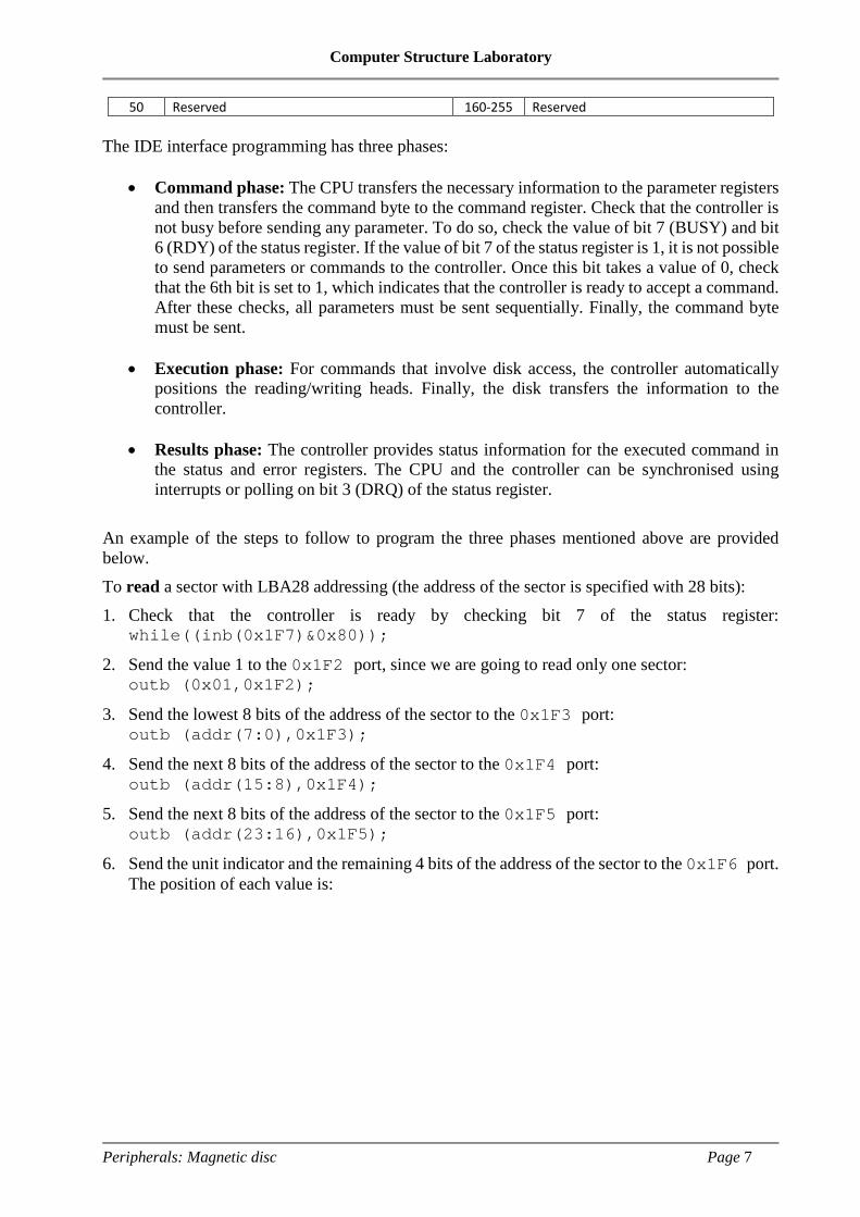
Computer Structure Laboratory
Peripherals: Magnetic disc Page 7
50 Reserved 160-255 Reserved The IDE interface programming has three phases:
• Command phase: The CPU transfers the necessary information to the parameter registers and then transfers the command byte to the command register. Check that the controller is not busy before sending any parameter. To do so, check the value of bit 7 (BUSY) and bit 6 (RDY) of the status register. If the value of bit 7 of the status register is 1, it is not possible to send parameters or commands to the controller. Once this bit takes a value of 0, check that the 6th bit is set to 1, which indicates that the controller is ready to accept a command. After these checks, all parameters must be sent sequentially. Finally, the command byte must be sent.
• Execution phase: For commands that involve disk access, the controller automatically
positions the reading/writing heads. Finally, the disk transfers the information to the controller.
• Results phase: The controller provides status information for the executed command in
the status and error registers. The CPU and the controller can be synchronised using interrupts or polling on bit 3 (DRQ) of the status register.
An example of the steps to follow to program the three phases mentioned above are provided below. To read a sector with LBA28 addressing (the address of the sector is specified with 28 bits): 1. Check that the controller is ready by checking bit 7 of the status register:
while((inb(0x1F7)&0x80));
2. Send the value 1 to the 0x1F2 port, since we are going to read only one sector: outb (0x01,0x1F2);
3. Send the lowest 8 bits of the address of the sector to the 0x1F3 port: outb (addr(7:0),0x1F3);
4. Send the next 8 bits of the address of the sector to the 0x1F4 port: outb (addr(15:8),0x1F4);
5. Send the next 8 bits of the address of the sector to the 0x1F5 port: outb (addr(23:16),0x1F5);
6. Send the unit indicator and the remaining 4 bits of the address of the sector to the 0x1F6 port. The position of each value is:
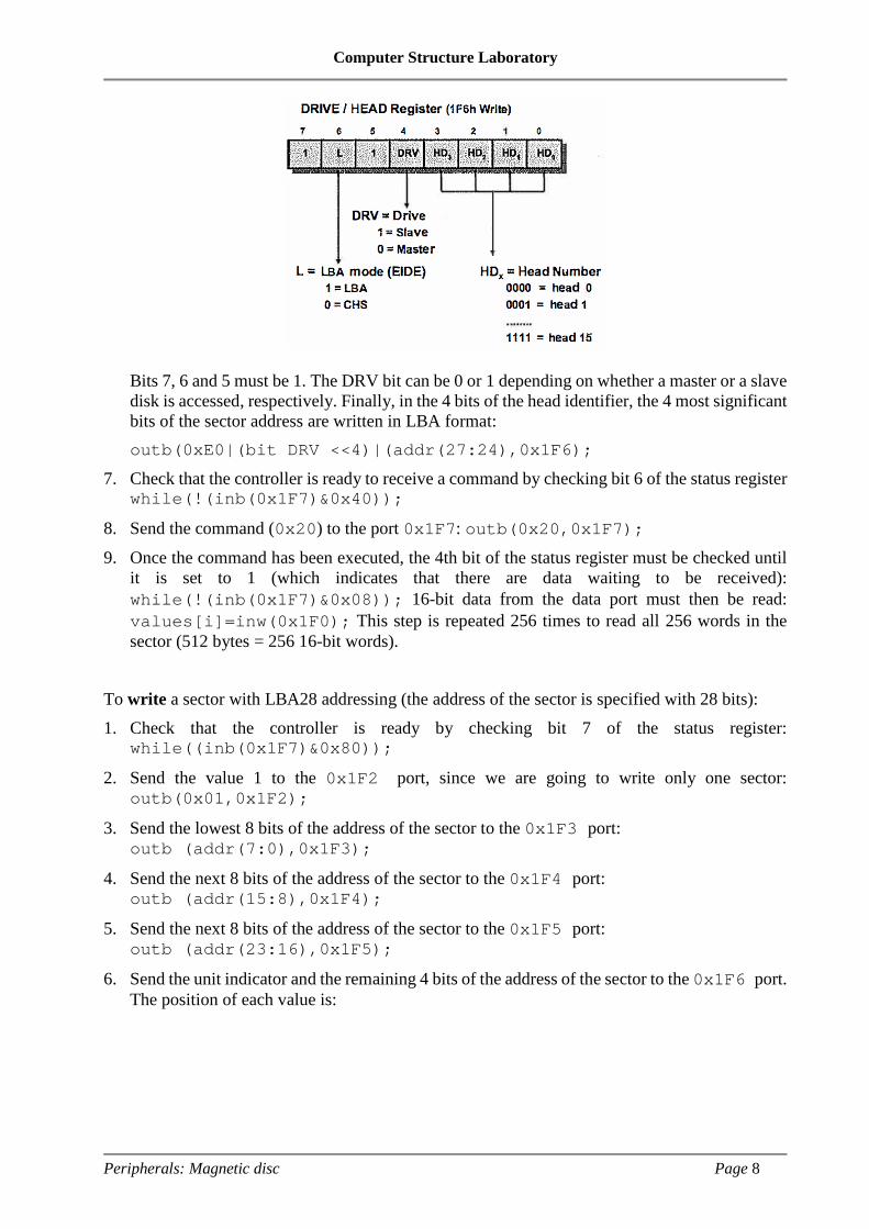
Computer Structure Laboratory
Peripherals: Magnetic disc Page 8
Bits 7, 6 and 5 must be 1. The DRV bit can be 0 or 1 depending on whether a master or a slave disk is accessed, respectively. Finally, in the 4 bits of the head identifier, the 4 most significant bits of the sector address are written in LBA format: outb(0xE0|(bit DRV <<4)|(addr(27:24),0x1F6);
7. Check that the controller is ready to receive a command by checking bit 6 of the status register while(!(inb(0x1F7)&0x40));
8. Send the command (0x20) to the port 0x1F7: outb(0x20,0x1F7);
9. Once the command has been executed, the 4th bit of the status register must be checked until it is set to 1 (which indicates that there are data waiting to be received): while(!(inb(0x1F7)&0x08)); 16-bit data from the data port must then be read: values[i]=inw(0x1F0); This step is repeated 256 times to read all 256 words in the sector (512 bytes = 256 16-bit words).
To write a sector with LBA28 addressing (the address of the sector is specified with 28 bits): 1. Check that the controller is ready by checking bit 7 of the status register:
while((inb(0x1F7)&0x80));
2. Send the value 1 to the 0x1F2 port, since we are going to write only one sector: outb(0x01,0x1F2);
3. Send the lowest 8 bits of the address of the sector to the 0x1F3 port: outb (addr(7:0),0x1F3);
4. Send the next 8 bits of the address of the sector to the 0x1F4 port: outb (addr(15:8),0x1F4);
5. Send the next 8 bits of the address of the sector to the 0x1F5 port: outb (addr(23:16),0x1F5);
6. Send the unit indicator and the remaining 4 bits of the address of the sector to the 0x1F6 port. The position of each value is:
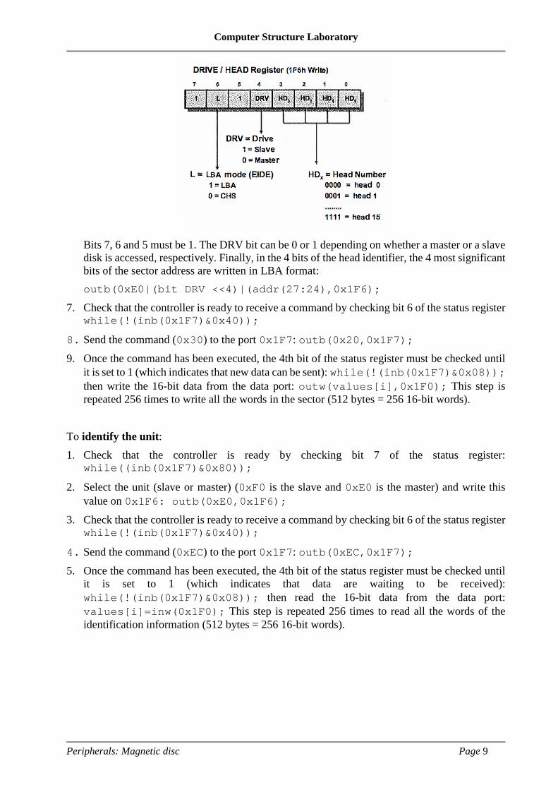
Computer Structure Laboratory
Peripherals: Magnetic disc Page 9
Bits 7, 6 and 5 must be 1. The DRV bit can be 0 or 1 depending on whether a master or a slave disk is accessed, respectively. Finally, in the 4 bits of the head identifier, the 4 most significant bits of the sector address are written in LBA format: outb(0xE0|(bit DRV <<4)|(addr(27:24),0x1F6);
7. Check that the controller is ready to receive a command by checking bit 6 of the status register while(!(inb(0x1F7)&0x40));
8. Send the command (0x30) to the port 0x1F7: outb(0x20,0x1F7);
9. Once the command has been executed, the 4th bit of the status register must be checked until it is set to 1 (which indicates that new data can be sent): while(!(inb(0x1F7)&0x08)); then write the 16-bit data from the data port: outw(values[i],0x1F0); This step is repeated 256 times to write all the words in the sector (512 bytes = 256 16-bit words).
To identify the unit: 1. Check that the controller is ready by checking bit 7 of the status register:
while((inb(0x1F7)&0x80));
2. Select the unit (slave or master) (0xF0 is the slave and 0xE0 is the master) and write this value on 0x1F6: outb(0xE0,0x1F6);
3. Check that the controller is ready to receive a command by checking bit 6 of the status register while(!(inb(0x1F7)&0x40));
4. Send the command (0xEC) to the port 0x1F7: outb(0xEC,0x1F7);
5. Once the command has been executed, the 4th bit of the status register must be checked until it is set to 1 (which indicates that data are waiting to be received): while(!(inb(0x1F7)&0x08)); then read the 16-bit data from the data port: values[i]=inw(0x1F0); This step is repeated 256 times to read all the words of the identification information (512 bytes = 256 16-bit words).
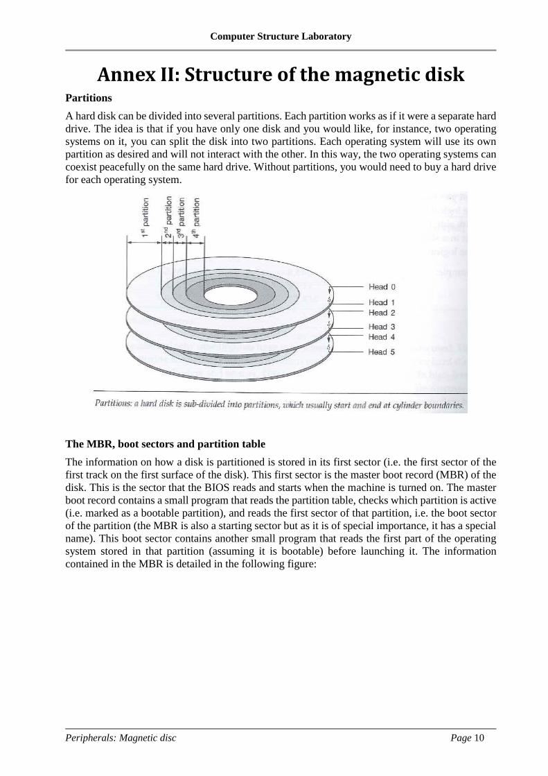
Computer Structure Laboratory
Peripherals: Magnetic disc Page 10
Annex II: Structure of the magnetic disk Partitions A hard disk can be divided into several partitions. Each partition works as if it were a separate hard drive. The idea is that if you have only one disk and you would like, for instance, two operating systems on it, you can split the disk into two partitions. Each operating system will use its own partition as desired and will not interact with the other. In this way, the two operating systems can coexist peacefully on the same hard drive. Without partitions, you would need to buy a hard drive for each operating system.
The MBR, boot sectors and partition table The information on how a disk is partitioned is stored in its first sector (i.e. the first sector of the first track on the first surface of the disk). This first sector is the master boot record (MBR) of the disk. This is the sector that the BIOS reads and starts when the machine is turned on. The master boot record contains a small program that reads the partition table, checks which partition is active (i.e. marked as a bootable partition), and reads the first sector of that partition, i.e. the boot sector of the partition (the MBR is also a starting sector but as it is of special importance, it has a special name). This boot sector contains another small program that reads the first part of the operating system stored in that partition (assuming it is bootable) before launching it. The information contained in the MBR is detailed in the following figure:
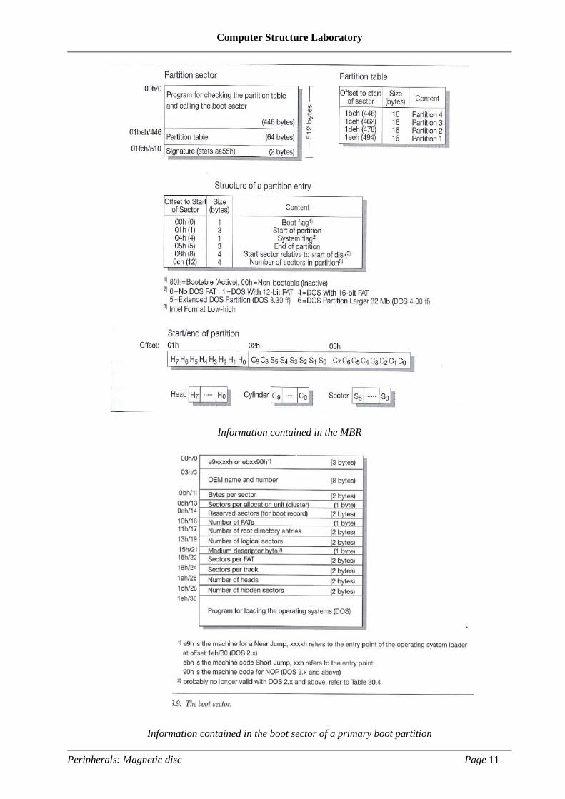
Computer Structure Laboratory
Peripherals: Magnetic disc Page 11
Information contained in the MBR
Information contained in the boot sector of a primary boot partition
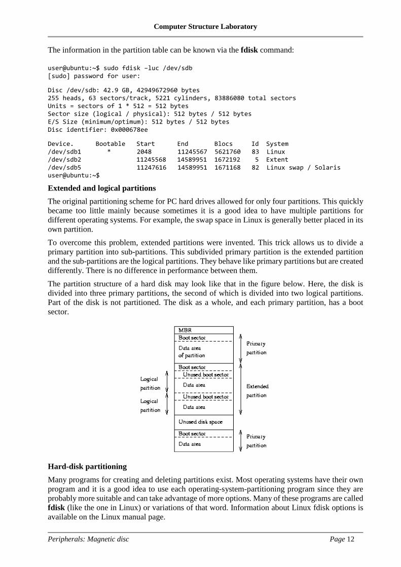
Computer Structure Laboratory
Peripherals: Magnetic disc Page 12
The information in the partition table can be known via the fdisk command: user@ubuntu:~$ sudo fdisk –luc /dev/sdb [sudo] password for user: Disc /dev/sdb: 42.9 GB, 42949672960 bytes 255 heads, 63 sectors/track, 5221 cylinders, 83886080 total sectors Units = sectors of 1 * 512 = 512 bytes Sector size (logical / physical): 512 bytes / 512 bytes E/S Size (minimum/optimum): 512 bytes / 512 bytes Disc identifier: 0x000678ee Device. Bootable Start End Blocs Id System /dev/sdb1 * 2048 11245567 5621760 83 Linux /dev/sdb2 11245568 14589951 1672192 5 Extent /dev/sdb5 11247616 14589951 1671168 82 Linux swap / Solaris user@ubuntu:~$
Extended and logical partitions The original partitioning scheme for PC hard drives allowed for only four partitions. This quickly became too little mainly because sometimes it is a good idea to have multiple partitions for different operating systems. For example, the swap space in Linux is generally better placed in its own partition. To overcome this problem, extended partitions were invented. This trick allows us to divide a primary partition into sub-partitions. This subdivided primary partition is the extended partition and the sub-partitions are the logical partitions. They behave like primary partitions but are created differently. There is no difference in performance between them. The partition structure of a hard disk may look like that in the figure below. Here, the disk is divided into three primary partitions, the second of which is divided into two logical partitions. Part of the disk is not partitioned. The disk as a whole, and each primary partition, has a boot sector.
Hard-disk partitioning Many programs for creating and deleting partitions exist. Most operating systems have their own program and it is a good idea to use each operating-system-partitioning program since they are probably more suitable and can take advantage of more options. Many of these programs are called fdisk (like the one in Linux) or variations of that word. Information about Linux fdisk options is available on the Linux manual page.
Computer Structure Laboratory
Peripherals: Magnetic disc Page 13
Annex III: Example program Example program #include <stdio.h> #include <stdlib.h> #include <sys/io.h> int main(int argc, char **argv) { int i,result; int values[256]; /* This vector is going to store the 256 words that the unit delivers in the results phase of the identify unit command. */ result=iopl(3); if(result != 0) printf("Port reservation error "); /* We wait until the disk controller is ready */ while((inb(0x1F7) & 0x80)); /* The disk on which we are going to operate is chosen. The value 0xF0 has the bit DRV = 1 means slave disk (we operate on / dev / sdb)*/ outb(0xF0,0x1F6); /* We wait until the disk is ready to receive a command, if the requested disk does not exist it will never be ready */ while(!(inb(0x1F7) & 0x40)); /*Send the command 0xEC => ATA IDENTIFY Command*/ outb(0xEC,0x1F7); for(i=0;i<256;i++){ /* 256 words are read => 512 bytes */ /* First, we wait until data are available */ while(!(inb(0x1F7) & 0x08)); /* A 16-bit word is read from port 0x1F0)*/ values[i]=inw(0x1F0); /* The information is printed byte by byte in Hexadecimal */ printf("%d:%02x \n",i*2,(values[i] % 256)); printf("%d:%02x \n",i*2+1,(values[i] / 256)); } iopl(0); exit(0); }
The C functions used are described below. Some of them were already used in the previous laboratory session.
Computer Structure Laboratory
Peripherals: Magnetic disc Page 14
iopl. The iopl function is used to access the input/output ports from the application by sending it a 3 as the only parameter (the man iopl command can be used in the command console to obtain more information about this). The iopl function is included in the sys/io.h library. 0 is returned if the action is successful and -1 is returned otherwise. The application (executable program) must be executed with root permissions (administrator). To have root permissions, the program must be run as: "sudo program_name". The root password will then be requested, which for our virtual machine is "passuser": int iopl(int level);
• inb and outb. The inb and outb functions are used to access the ports. The sys/io.h and stdio.h libraries must be included in the program (to be able to use both functions) and in the basic input/output functions. The prototypes for these functions are: unsigned char inb(unsigned short port);
/* It reads an 8-bit value from the specified port */
void outb (unsigned char valor, unsigned short port);
/* It writes an 8-bit value on the specified port */
• inw and outw. These are the same as the previous ones but are used to access 16-bit data.
Computer Structure Laboratory
Peripherals: graphic card Page 1
Laboratory 8: Peripherals:
Graphic card (Updated at 29/01/2019)
Work at home (planned) time: 1:30h Lab time: 2:30h
1. Introduction In this laboratory session we will study how a computer graphic card works and how the card’s memory is accessed to display images on screen. Examples with several graphic card resolutions will be shown. We will also study how the resolution affects how the card’s video memory is accessed and how the colour palette is selected. Several programs in C will be implemented to operate with the graphics card (using the Svgalib library to help establish configuration), which is available for several Linux distributions.
Goal On completion of this laboratory session you will be able to - understand the structure of the video memory and how it is accessed, - change the graphic card’s resolution and understand how the various resolutions change the way the card’s memory is accessed, - use the library functions that come with the Svgalib package to change the resolution of the card and the colour palette, - design and implement C programs that can perform low-level access to the video card.
Resources We will use the same virtual machine as in the previous laboratory session. To run the virtual machine, the VMware player software needs to be installed. This software is free and can be downloaded from the VMware company website. The Linux virtual machine has all the necessary software pre-installed for compiling and executing the programs that must be implemented in the session. You can find more information about the Svgalib library at: http://linux.die.net/man/7/svgalib y http://www.svgalib.org/
2. Preliminary (pre-lab) work For this pre-lab work, all students in the workgroup must read annexes I, II and III of this document. Annex I describes the Svgalib library functions and provides an example code to show the implementation of a simple program using this library. Annex II shows how to compile the files in Linux. Annex III reviews the concepts outlined in the class notes regarding the VGA card.
Lab 8

Computer Structure Laboratory
Peripherals: graphic card Page 2
You should also review the concepts on computer graphic cards explained in Topic 3. After reading the annexes and class notes, answer the following questions:
Q1. Describe what the example program in Annex I does. Q2. Which pixels’ resolution is used by the example program in Annex I? Q3. How many colours can the video card display with the resolution set in the program in
Annex I without changing the colour palette. Q4. How many colours could we show if we changed the colour palette? Q5. Which colours are set in the palette as first and second colours?
Q6. What is the unsigned char *vbuf pointer used for?
Q7. What is the vga_getgraphmem()function for?
Q8. What does the program do in the loop for (k=0; k<10; k++)? Justify your answer with a reasoned explanation.
First checkpoint: Q1-Q8 must be written up and handed in to your lecturer at the beginning of the session. You must be able to justify your answers.
3. Lab (in-lab) workIn this session we will study the low-level programming and management of the VGA graphic card in a practical way to understand its possibilities and limitations. To do so we will design several programs that require the use of this peripheral.
3.1 The program in Annex I must be compiled in a shell of the virtual machine as explained in the instructions provided in Annex II. Check that the program works correctly.
3.2 Design a program in C that configures the graphics card in G320x200x256 mode, i.e. a graphic mode of 320x200 pixels and 256 colours. Then initialise a pointer to the start position of the frame buffer. The colour palette must also be configured so that colour 0 is black and colour 1 is white. Once the configuration is established, the program should flash a 9x14 pixel array located in the upper left-hand corner of the screen. The blinking frequency must be set to 2 seconds. This means that the pixels in the matrix will be set for 1 second in white and 1 second in black. The pixel must remain blinking for 10 seconds. Execute the program and answer the following questions with reasoned arguments:
3.2.1 How many memory positions do you have to move in order to write on pixels that are located in the same column?
3.2.2 With this configuration, how much memory do we need to implement the frame buffer? To verify your answer to this question, make the program blink all the pixels on the screen.
Second checkpoint: Show the lecturer that the program works properly. Be able to answer the above or any other questions related to this subject.

Computer Structure Laboratory
Peripherals: graphic card Page 3
3.3 Implement a C program to configure the card in G1024x768x256 mode, i.e. a graphic mode of 1024x768 pixels and 256 colours. Next initialise a pointer to the start position of the frame buffer. The colour palette must be set so that the 256 colours show only a continuous gradient of blue shades from darkest to lightest (since there can only be 64 different tones, these values must be repeated 4 times until the 256 colour registers are filled). Implement a program that shows every tone of the palette sequentially by rows of pixels, i.e. the first pixel should have the colour for register 0 of the palette, the second pixel should have the colour for register 1, etc. When the end of the palette is reached, it should start again with index colour register 0. The program should fill the screen with the palette’s colours. Bear in mind that each time 64 KBytes of memory are loaded from the frame buffer, the bank must be changed with the vga_setpage function (int number_of_page); to continue accessing the next pixel positions. You must therefore begin writing again from the pointer’s initial position to the frame buffer. At the end, a wait function must be included to view the result of the writing. Run the program and answer the following questions:
3.3.1 How many times do you have to change the page to complete the writing on the whole screen in this graphic mode?
3.3.2 How many times are the colours repeated in the same row on the screen? 3.3.3 We can reduce the number of pixels with a repeated colour in each line by adding more
colours (not just shades of blue). What is the minimum number of repetitions we can have in the same row?
Third checkpoint: Show the lecturer that the program works properly. Be able to answer any questions on its design and operation.
All answers to the questions must be written up and handed in to the lecturer before you leave the laboratory.
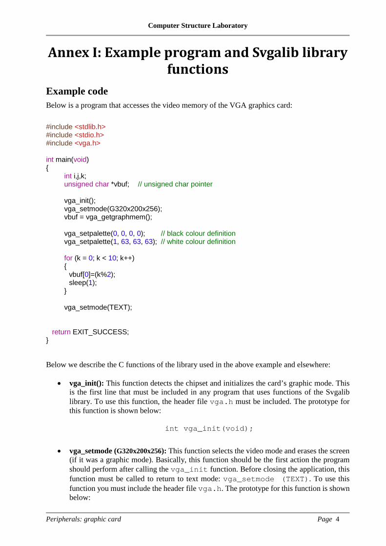
Computer Structure Laboratory
Peripherals: graphic card Page 4
Annex I: Example program and Svgalib library functions
Example code Below is a program that accesses the video memory of the VGA graphics card: #include <stdlib.h> #include <stdio.h> #include <vga.h> int main(void) { int i,j,k; unsigned char *vbuf; // unsigned char pointer vga_init(); vga_setmode(G320x200x256); vbuf = vga_getgraphmem(); vga_setpalette(0, 0, 0, 0); // black colour definition vga_setpalette(1, 63, 63, 63); // white colour definition for (k = 0; k < 10; k++) { vbuf[0]=(k%2); sleep(1); } vga_setmode(TEXT); return EXIT_SUCCESS; }
Below we describe the C functions of the library used in the above example and elsewhere:
• vga_init(): This function detects the chipset and initializes the card’s graphic mode. This is the first line that must be included in any program that uses functions of the Svgalib library. To use this function, the header file vga.h must be included. The prototype for this function is shown below:
int vga_init(void);
• vga_setmode (G320x200x256): This function selects the video mode and erases the screen
(if it was a graphic mode). Basically, this function should be the first action the program should perform after calling the vga_init function. Before closing the application, this function must be called to return to text mode: vga_setmode (TEXT). To use this function you must include the header file vga.h. The prototype for this function is shown below:

Computer Structure Laboratory
Peripherals: graphic card Page 5
int vga_setmode(int mode);
• vga_getgraphmem(): This function returns a pointer to the starting address of the frame
buffer in the video memory of the VGA card. To use this function, you must include the header file vga.h. This window is 64 KB. The prototype for this function is shown below:
unsigned char *vga_getgraphmem(void);
• vga_setpalette(0, 0, 0, 0): This function modifies the colour of the index position in the current RGB colour palette. The last 3 parameters indicate the level of the red (R), green (G) and blue (B) components of the pixel, respectively. Each of these values can be set in the 0-63 range, where 0 means zero brightness for this component and 63 means maximum brightness. To use this function, you must include the header file vga.h. This function can be applied only in 16 or 256 colour modes.
void vga_setpalette(int index, int r, int g, int b);
• void vga_setpage(int page): The SVGA cards have more than 64 KBytes of memory. However, the window of the memory that the CPU can access at a given time is only 64 KBytes. The vga_setpage() function selects a 64KB memory page, inside the card’s memory, as a memory block that is visible to the microprocessor and which the user program can access by starting a pointer with the vga_getgraphmem() function.
void vga_setpage(int page);

Computer Structure Laboratory
Peripherals: graphic card Page 6
Annex II: Compilation in Linux To run the Linux virtual machine, you must follow the same methodology as in the previous two sessions. Once the programs have been completed in the editor, they must be saved with the extension *.c in the user directory (/home/user) or in a subfolder. To do so, the Places menu can be used to open a file browser and help you to manage the directories and files). To compile the programs in this laboratory session, you must enter the command in the terminal: gcc -o executable-file source-file.c -lvga
The executable file will be the output file. This file must not have an extension. To execute the file, we must have root privileges. We will therefore execute the program in the same directory as the executable file with the command: sudo ./executable-file
This command will ask for the root password, which is the same as in previous sessions, i.e. "passuser".
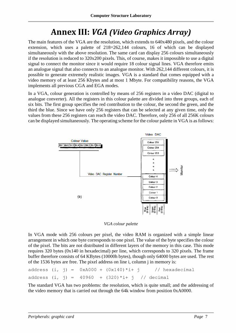
Computer Structure Laboratory
Peripherals: graphic card Page 7
Annex III: VGA (Video Graphics Array) The main features of the VGA are the resolution, which extends to 640x480 pixels, and the colour extension, which uses a palette of 218=262,144 colours, 16 of which can be displayed simultaneously with the above resolution. The same card can display 256 colours simultaneously if the resolution is reduced to 320x200 pixels. This, of course, makes it impossible to use a digital signal to connect the monitor since it would require 18 colour signal lines. VGA therefore emits an analogue signal that also connects to an analogue monitor. With 262,144 different colours, it is possible to generate extremely realistic images. VGA is a standard that comes equipped with a video memory of at least 256 Kbytes and at most 1 Mbyte. For compatibility reasons, the VGA implements all previous CGA and EGA modes. In a VGA, colour generation is controlled by means of 256 registers in a video DAC (digital to analogue converter). All the registers in this colour palette are divided into three groups, each of six bits. The first group specifies the red contribution to the colour, the second the green, and the third the blue. Since we have only 256 registers that can be selected at any given time, only the values from these 256 registers can reach the video DAC. Therefore, only 256 of all 256K colours can be displayed simultaneously. The operating scheme for the colour palette in VGA is as follows:
VGA colour palette
In VGA mode with 256 colours per pixel, the video RAM is organized with a simple linear arrangement in which one byte corresponds to one pixel. The value of the byte specifies the colour of the pixel. The bits are not distributed in different layers of the memory in this case. This mode requires 320 bytes (0x140 in hexadecimal) per line, which corresponds to 320 pixels. The frame buffer therefore consists of 64 KBytes (10000h bytes), though only 64000 bytes are used. The rest of the 1536 bytes are free. The pixel address on line i, column j in memory is: address (i, j) = 0xA000 + (0x140)*i+ j // hexadecimal
address (i, j) = 40960 + (320)*i+ j // decimal
The standard VGA has two problems: the resolution, which is quite small; and the addressing of the video memory that is carried out through the 64k window from position 0xA0000.
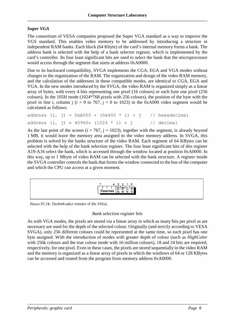
Computer Structure Laboratory
Peripherals: graphic card Page 8
Super VGA The consortium of VESA companies proposed the Super VGA standard as a way to improve the VGS standard. This enables video memory to be addressed by introducing a structure in independent RAM banks. Each block (64 Kbyte) of the card’s internal memory forms a bank. The address bank is selected with the help of a bank selector register, which is implemented by the card’s controller. Its four least significant bits are used to select the bank that the microprocessor would access through the segment that starts at address 0xA0000. Due to its backward compatibility, SVGA implements the CGA, EGA and VGA modes without changes to the organization of the RAM. The organization and design of the video RAM memory, and the calculation of the addresses in these compatible modes, are identical to CGA, EGA and VGA. In the new modes introduced by the SVGA, the video RAM is organized simply as a linear array of bytes, with every 4 bits representing one pixel (16 colours) or each byte one pixel (256 colours). In the 105H mode (1024*768 pixels with 256 colours), the position of the byte with the pixel in line i, column j (i = 0 to 767, j = 0 to 1023) in the 0xA000 video segment would be calculated as follows: address (i, j) = 0xA000 + (0x400 * i) + j // hexadecimal
address (i, j) = 40960+ (1024 * i) + j // decimal
As the last point of the screen (i = 767, j = 1023), together with the segment, is already beyond 1 MB, it would leave the memory area assigned to the video memory address. In SVGA, this problem is solved by the banks structure of the video RAM. Each segment of 64 KBytes can be selected with the help of the bank selection register. The four least significant bits of this register A19-A16 select the bank, which is accessed through the window located at position 0xA0000. In this way, up to 1 Mbyte of video RAM can be selected with the bank structure. A register inside the SVGA controller controls the bank that forms the window connected to the bus of the computer and which the CPU can access at a given moment.
Bank selection register bits As with VGA modes, the pixels are stored via a linear array in which as many bits per pixel as are necessary are used for the depth of the selected colour. Originally (and strictly according to VESA SVGA), only 256 different colours could be represented at the same time, so each pixel has one byte assigned. With the introduction of modes with greater depth of colour (such as HighColor with 256k colours and the true colour mode with 16 million colours), 18 and 24 bits are required, respectively, for one pixel. Even in these cases, the pixels are stored sequentially in the video RAM and the memory is organized as a linear array of pixels in which the windows of 64 or 128 KBytes can be accessed and routed from the program from memory address 0xA0000.