INVESTIGATION OF HIGH PERFORMANCE SINGLE-PHASE ...
148
INVESTIGATION OF HIGH PERFORMANCE SINGLE-PHASE SOLUTIONS FOR AC-DC POWER FACTOR CORRECTED BOOST CONVERTERS by Fariborz Musavi M.A.Sc., Concordia University, 2001 B.Sc., Iran University of Science and Technology, 1994 A THESIS SUBMITTED IN PARTIAL FULFILLMENT OF THE REQUIREMENTS FOR THE DEGREE OF DOCTOR OF PHILOSOPHY in The Faculty of Graduate Studies (Electrical and Computer Engineering) THE UNIVERSITY OF BRITISH COLUMBIA (Vancouver) May 2011 © Fariborz Musavi, 2011
-
Upload
khangminh22 -
Category
Documents
-
view
0 -
download
0
Transcript of INVESTIGATION OF HIGH PERFORMANCE SINGLE-PHASE ...

INVESTIGATION OF HIGH PERFORMANCE SINGLE-PHASE
SOLUTIONS FOR AC-DC POWER FACTOR CORRECTED BOOST
CONVERTERS
by
Fariborz Musavi
M.A.Sc., Concordia University, 2001
B.Sc., Iran University of Science and Technology, 1994
A THESIS SUBMITTED IN PARTIAL FULFILLMENT OF
THE REQUIREMENTS FOR THE DEGREE OF
DOCTOR OF PHILOSOPHY
in
The Faculty of Graduate Studies
(Electrical and Computer Engineering)
THE UNIVERSITY OF BRITISH COLUMBIA
(Vancouver)
May 2011
© Fariborz Musavi, 2011

ii
Abstract
Plug-in Hybrid Electric Vehicles (PHEVs) and Electric Vehicles (EVs) are an emerging
trend in automotive circles, and consumer’s interest is growing rapidly. With the development of
PHEVs, battery chargers for automotive applications are becoming a large market for the power
supply industries. The improvement of overall charger efficiency is critical for the emergence
and acceptance of these vehicular technologies, as the charger efficiency increases, the charge
time and utility cost decreases. Additionally, to meet the efficiency and power factor
requirements and regulatory standards for the AC supply mains, power factor correction is
essential.
Due to limited space in vehicle and increasing power consumption, chargers are required
to deliver more power with smaller volume. As a key component of a charger system, the front-
end AC-DC converter must achieve high efficiency and high power density. In this dissertation,
several conventional plug in hybrid electric vehicle charger front end AC-DC converter
topologies are investigated and a new bridgeless interleaved and a phase shifted semi-bridgeless
power factor corrected converter are proposed to improve the efficiency and performance, which
is critical to minimize the charger size, charging time, and the amount and cost of electricity
drawn from the utility. A detailed analytical model for these topologies is developed, enabling
the calculation of power losses and efficiency. Experimental and simulation results of several
prototype boost converter converting universal AC input voltage to 400 V DC at 3.4 kW are
given to verify the proof of concept, and analytical work reported in this thesis. The results show
a power factor greater than 0.99 from 750 W to 3.4 kW, THD less than 5% from half load to full
load and a peak efficiency of 98.94 % at 265 V input and 1200 W load.
iii
Preface
This thesis contains four chapters that present results that have been published or
submitted for consideration in the form of IEEE refereed papers and scientific journals of which
I am the lead author. The initial project overview was proposed by me. For the scientific journal
submissions and papers, I performed all the research, data analyses, and interpretation of the
results, and prepared the final manuscripts. Co-authors provided advice on methodology and
made editorial comments as required. The complete citations for these papers and the chapters in
which they appear are provided as follows:
Chapter 2 is based on:
[1] F. Musavi ; W. Eberle ; W.G. Dunford, "A High-Performance Single-Phase AC-DC Power
Factor Corrected Boost Converter for plug in Hybrid Electric Vehicle Battery Chargers,"
Published in IEEE Energy Conversion Congress and Exposition, Atlanta, Georgia, 2010.
[2] F. Musavi ; W. Eberle ; W.G. Dunford, "Efficiency Evaluation of Single-Phase Solutions for
AC-DC PFC Boost Converters for Plug-in-Hybrid Electric Vehicle Battery Chargers," Published
in IEEE Vehicle Power and Propulsion Conference, Lille, France, 2010.
[3] F. Musavi ; W. Eberle ; W.G. Dunford, "A High-Performance Single-Phase Bridgeless
Interleaved PFC Converter for Plug-in Hybrid Electric Vehicle Battery Chargers," IEEE
Transactions on Industry Applications, in press, 2010-IPCC-417.R1 (T-IA).
Chapter 3 is based on:
[4] F. Musavi ; W. Eberle ; W.G. Dunford, "A Phase Shifted Semi-Bridgeless Boost Power
Factor Corrected Converter for Plug in Hybrid Electric Vehicle Battery Chargers," Published in
IEEE Applied Power Electronics Conference and Exposition, APEC, Fort Worth, TX, 2011.

iv
Chapter 4 is based on:
[5] F. Musavi ; M. Edington ; W. Eberle ; W.G. Dunford, "Effect of Ripple Steering Technique
on Control Loop Stability of A CCM PFC Boost Converter," Published in IEEE Energy
Conversion Congress and Exposition, Phoenix, AZ, 2011.
Part of Chapter 1, Chapter 2 and Chapter 3 are based on:
[6] F. Musavi ; M. Edington ; W. Eberle ; W.G. Dunford, "Energy Efficiency in Plug in Hybrid
Electric Vehicle Chargers: Evaluation and Comparison of Front End AC-DC Topologies,"
Published in IEEE Energy Conversion Congress and Exposition, Phoenix, AZ, 2011.
[7] D. Gautam ; F. Musavi ; M. Edington ; W. Eberle ; W.G. Dunford, " An Automotive On-
Board 3.3 kW Battery Charger for PHEV Application," Published in IEEE Vehicle Power and
Propulsion Conference, Chicago, IL, 2011.

v
Table of Contents
Abstract ................................................................................................................................................... ii
Preface ................................................................................................................................................... iii
Table of Contents .................................................................................................................................... v
List of Tables ....................................................................................................................................... viii
List of Figures ........................................................................................................................................ ix
List of Symbols .................................................................................................................................... xiv
Acknowledgements ............................................................................................................................. xvii
Dedication .......................................................................................................................................... xviii
CHAPTER 1. Introduction .................................................................................................................. 1
1.1. Introduction ............................................................................................................................. 1
1.2. General Background ................................................................................................................. 3
1.3. Literature Review ..................................................................................................................... 6
1.3.1. Conventional PFC Boost Converter .................................................................................. 8
1.3.2. Bridgeless PFC Boost Converter ..................................................................................... 11
1.3.2.1. Positive "HALF Cycle" Operation .............................................................................. 12
1.3.2.2. Negative "HALF Cycle" Operation ............................................................................. 12
1.3.2.1. PSIM Simulation of Bridgeless Boost Converter ......................................................... 14
1.3.3. Semi-Bridgeless PFC boost Converter ............................................................................ 15
1.3.4. Interleaved PFC Boost Converter .................................................................................... 16
1.3.4.1. PSIM Simulation of Interleaved Boost Converter ........................................................ 18
1.3.5. Ripple Steering Technique in PFC Applications.............................................................. 19
1.3.6. Average Switch Model ................................................................................................... 21
1.4. Motivation and Objectives of the Thesis ................................................................................. 22
1.5. Outline of the Thesis .............................................................................................................. 23
CHAPTER 2. Bridgeless Interleaved PFC Boost Converter ............................................................... 24
2.1. Introduction ........................................................................................................................... 24
2.2. Circuit Description and Steady State Analysis ........................................................................ 24
2.2.1. Positive Half Cycle Operation ........................................................................................ 25
2.2.2. Negative Half Cycle Operation ....................................................................................... 25
2.2.3. Detailed Positive Half Cycle Operation and Analysis for D > 0.5 .................................... 26

vi
2.2.4. Detailed Positive Half Cycle Operation and Analysis for D < 0.5 .................................... 30
2.3. Loss Modeling ....................................................................................................................... 35
2.4. Math Modeling Verification ................................................................................................... 41
2.5. Simulation Results ................................................................................................................. 45
2.6. Logic Implementation ............................................................................................................ 47
2.7. Experimental Results.............................................................................................................. 49
2.8. Conclusion ............................................................................................................................. 57
CHAPTER 3. Phase-Shifted Semi Bridgeless PFC Converter ............................................................ 59
3.1. Introduction ........................................................................................................................... 59
3.2. Circuit Description and Steady State Analysis ........................................................................ 59
3.2.1. Positive Half Cycle Operation ........................................................................................ 60
3.2.2. Negative Half Cycle Operation ....................................................................................... 61
3.2.1. Detailed Positive Half Cycle Operation and Analysis for D > 0.5 .................................... 61
3.2.1. Detailed Positive Half Cycle Operation and Analysis for D < 0.5 .................................... 64
3.3. Loss Modeling ....................................................................................................................... 66
3.4. Simulation Results ................................................................................................................. 68
3.5. Logic Implementation ............................................................................................................ 70
3.6. Experimental Results.............................................................................................................. 71
3.7. Conclusion ............................................................................................................................. 82
CHAPTER 4. The Ripple Steering Technique and Converter Modeling ............................................ 83
4.1. Introduction ........................................................................................................................... 83
4.2. Average Switch Model ........................................................................................................... 83
4.2.1. PWM Switch Model of Conventional Boost Converter ................................................... 83
4.2.1. Feedback Compensation Design of Conventional Boost Converter ................................. 84
4.3. Ripple Steering Techniques in PFC Application ..................................................................... 88
4.3.1. PWM Switch Model of Boost Converter with Coupled Inductor ..................................... 89
4.3.1. Feedback Compensation Design of Boost Converter with Coupled Inductor ................... 92
4.4. Simulation Results ................................................................................................................. 93
4.5. Experimental Results.............................................................................................................. 95
4.6. Conclusion ........................................................................................................................... 102
CHAPTER 5. Conclusions and Future Work ................................................................................... 103
5.1. Conclusions ......................................................................................................................... 103

vii
5.1.1. Bridgeless Interleaved Boost PFC Converter................................................................. 103
5.1.2. Phase Shifted Semi-Bridgeless Boost PFC Converter .................................................... 103
5.1.3. New Loss Modeling for PFC Boost Converters ............................................................. 104
5.1.1. New Average Modeling for PFC Boost Converters with Coupled Inductors .................. 104
5.2. Future Work ......................................................................................................................... 105
5.2.1. LLC Resonant Converter for DC/DC Stage................................................................... 105
5.2.2. Resonant PFC Converter .............................................................................................. 105
5.2.3. Level 3 Chargers .......................................................................................................... 105
5.2.4. Wireless Chargers......................................................................................................... 106
Bibliography ....................................................................................................................................... 107
Appendix ............................................................................................................................................ 112

viii
List of Tables
Table 2-1: Summary of component RMS current for conventional boost and bridgeless boost topologies
...................................................................................................................................................... 37
Table 2-2: Summary of component RMS current for interleaved and bridgeless interleaved boost
topologies ...................................................................................................................................... 37
Table 2-3: Summary of component average current for conventional boost and bridgeless boost
topologies ...................................................................................................................................... 38
Table 2-4: Summary of component average current for interleaved and bridgeless interleaved boost
topologies ...................................................................................................................................... 38
Table 2-5: Component / devices used in prototype unit .......................................................................... 52
Table 3-1: Component / devices used in prototype unit .......................................................................... 71
ix
List of Figures
Figure 1-1: Simplified system block diagram of a universal two-stage battery charger ............................. 3
Figure 1-2: Passive power factor correction AC main voltage and current waveforms .............................. 5
Figure 1-3: Conventional PFC boost converter......................................................................................... 8
Figure 1-4: Simplified block diagram of the boost PFC circuit ................................................................. 9
Figure 1-5: Inductor current and the duty cycle in a typical PFC boost converter in CCM ...................... 10
Figure 1-6: Top: Transistor current - Bottom: Diode current in a typical PFC boost converter in CCM ... 10
Figure 1-7: Bridgeless PFC boost topology ............................................................................................ 11
Figure 1-8: Bridgeless PFC converter operation ..................................................................................... 13
Figure 1-9: PSIM simulation circuit for bridgeless PFC boost converter: Vin = 240V, Vo = 400V, Po =
3400W and fsw = 70 kHz .............................................................................................................. 14
Figure 1-10: Simulation waveforms for bridgeless PFC boost converter including output voltage, input
voltage and input current: Vin = 240V, Vo = 400V, Po = 3400W and fsw = 70 kHz ....................... 15
Figure 1-11: Bridgeless PFC boost topology .......................................................................................... 16
Figure 1-12: Interleaved PFC boost topology ......................................................................................... 17
Figure 1-13: PSIM simulation circuit for interleaved PFC boost converter: Vin = 240V, Vo = 400V, Po =
3400W and fsw = 70 kHz .............................................................................................................. 18
Figure 1-14: Simulation waveforms for interleaved PFC boost converter including output voltage, input
voltage and input current: Vin = 240V, Vo = 400V, Po = 3400W and fsw = 70 kHz ....................... 19
Figure 1-15: Smoothing transformer in a coupled filter .......................................................................... 20
Figure 1-16: Modified PFC boost converter with coupled inductors ....................................................... 20
Figure 1-17: One active switch and one passive switch .......................................................................... 21
Figure 1-18: PWM-switch ..................................................................................................................... 21
Figure 1-19: Averaged model of PWM-switch ....................................................................................... 21
Figure 2-1: Proposed bridgeless interleaved (BLIL) PFC boost converter ............................................... 25
Figure 2-2: Interval 1: Q1 and Q2 are “ON”, and body diode of Q4 conducting ..................................... 26
Figure 2-3: Interval 2 and 4: Q1, Q2, Q3 and Q4 are “ON” .................................................................... 26
Figure 2-4: Interval 3: Q3 and Q4 are “ON”, and body diode of Q2 conducting ..................................... 27
Figure 2-5: BLIL PFC boost converter steady-state waveforms at D > 0.5.............................................. 28
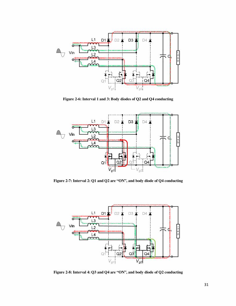
Figure 2-6: Interval 1 and 3: Body diodes of Q2 and Q4 conducting ...................................................... 31
Figure 2-7: Interval 2: Q1 and Q2 are “ON”, and body diode of Q4 conducting ..................................... 31
Figure 2-8: Interval 4: Q3 and Q4 are “ON”, and body diode of Q2 conducting ..................................... 31
Figure 2-9: BLIL PFC boost converter steady-state waveforms at D < 0.5.............................................. 33

x
Figure 2-10: RMS ripple current through output capacitors vs input voltage at Po = 3400 W, fsw = 70
kHz ............................................................................................................................................... 39
Figure 2-11: Comparison of the estimated loss distribution in the semiconductors at 70kHz switching
frequency, 240V input, 3400W load at 400V ................................................................................. 40
Figure 2-12: Simulation and math modeling of inductor RMS current for an interleaved PFC converter . 42
Figure 2-13: Simulation and math modeling of MOSFET RMS current for an interleaved PFC converter
...................................................................................................................................................... 42
Figure 2-14: Simulation and math modeling of boost diode average current for an interleaved PFC
converter ....................................................................................................................................... 43
Figure 2-15: Simulation and math modeling of inductor RMS current for a bridgeless PFC converter .... 43
Figure 2-16: Simulation and math modeling of MOSFET RMS current for a bridgeless PFC converter .. 44
Figure 2-17: Simulation and math modeling of boost diode average current for a bridgeless PFC converter
...................................................................................................................................................... 44
Figure 2-18: Simulation and math modeling of MOSFET body diode average current for a bridgeless PFC
...................................................................................................................................................... 45
Figure 2-19: PSIM simulation circuit for the proposed BLIL PFC boost converter: Vin = 240V, Vo =
400V, Po = 3400W and fsw = 70 kHz ............................................................................................ 46
Figure 2-20: Simulation waveforms for the proposed BLIL PFC boost converter including output voltage,
input voltage and input current: Vin = 240V, Vo = 400V, Po = 3400W and fsw = 70 kHz .............. 47
Figure 2-21: Logic implementation of BLIL PFC boost converter using UCC28070 controller .............. 48
Figure 2-22: Breadboard prototype of BLIL PFC boost converter .......................................................... 49
Figure 2-23: Breadboard proposed BLIL PFC experimental waveforms; ................................................ 50
Figure 2-24: Gating signal, boost MOSFET and diode current for D > 0.5 ............................................. 50
Figure 2-25: Gating signal, boost MOSFET and diode current for D < 0.5 ............................................. 51
Figure 2-26: Load transient response from FL to NL (3400W to 0W) .................................................... 51
Figure 2-27: Load transient response from NL to FL (0W to 3400 W).................................................... 52
Figure 2-28: Input current harmonics at full load for Vin = 120 V at Po = 1700 W and 240 V at Po = 3400
W .................................................................................................................................................. 53
Figure 2-29: RMS Total harmonics distortion vs. output power at Vin = 120V and Vin = 240V ............. 53
Figure 2-30: Power factor vs. output power at Vin = 120V and Vin = 240V ........................................... 54
Figure 2-31: Efficiency vs. output power for the proposed bridgeless interleaved PFC boost converter .. 54
Figure 2-32: Efficiency vs. output power for different topologies at Vin = 240V .................................... 55
Figure 2-33: Loss reduction as a function of output power at Vin = 240V, Vo = 400 V and 70 kHz for the
proposed BLIL converter compared to the benchmark interleaved boost converter ......................... 56
xi
Figure 2-34: Loss reduction as a function of output power at Vin = 120V, Vo = 400 V and 70 kHz for the
proposed BLIL converter compared to the benchmark interleaved boost converter ......................... 57
Figure 3-1: Phase shifted semi-bridgeless PFC boost topology ............................................................... 60
Figure 3-2: Interval 1and 3: Q1 and Q2 are ON...................................................................................... 61
Figure 3-3: Interval 2: Q1 ON, body diode of Q2 conducting ................................................................. 62
Figure 3-4: Interval 4: Q1 OFF and Q2 ON............................................................................................ 62
Figure 3-5: Phase shifted semi-bridgeless boost converter steady-state waveforms at D > 0.5................. 63
Figure 3-6: Interval 1and 3: Q1 and Q2 are OFF, body diode of Q2 conducting ..................................... 64
Figure 3-7: Interval 2: Q1 ON, body diode of Q2 conducting ................................................................. 64
Figure 3-8: Interval 4: Q1 OFF and Q2 ON............................................................................................ 64
Figure 3-9: Phase shifted semi-bridgeless boost converter steady-state waveforms at D < 0.5................. 65
Figure 3-10: Comparison of the estimated loss distribution in the semiconductors at 70kHz switching
frequency, 240V input, 3300W load at 400V ................................................................................. 67
Figure 3-11: PSIM simulation circuit for the phase shifted semi-bridgeless PFC boost converter: Vin =
240V, Vo = 400V, Po = 3400W and fsw = 70 kHz ......................................................................... 68
Figure 3-12: Simulation waveforms for the proposed phase shifted semi-bridgeless PFC boost converter:
Output voltage, input voltage and input current: Vin = 240V, Vo = 400V, Po = 3400W and fsw = 70
kHz ............................................................................................................................................... 69
Figure 3-13: Logic implementation of phase shifted semi-bridgeless PFC boost converter using
UCC28070 controller ..................................................................................................................... 70
Figure 3-14: Capacitor bank of 820 uF................................................................................................... 72
Figure 3-15: Control board of PFC boost converter ................................................................................ 72
Figure 3-16: IMS power board attached to a heatsink with the PFC inductors ........................................ 73
Figure 3-17: Efficiency as a function of output power at Vin = 240V, Vo=400V and 70kHz switching .. 74
Figure 3-18: Loss reduction as a function of output power at Vin = 240V, Vo=400V and 70kHz for the
proposed phase shifted semi-bridgeless converter compared to the benchmark interleaved boost
converter ....................................................................................................................................... 74
Figure 3-19: Efficiency as a function of output power at Vin = 120V, Vo=400V and 70kHz .................. 75
Figure 3-20: Loss reduction as a function of output power at Vin = 120V, Vo=400V and 70kHz for the
proposed phase shifted semi-bridgeless converter compared to the benchmark interleaved boost
converter ....................................................................................................................................... 75
Figure 3-21: THD as a function of output power at Vin = 120 V and 240V, Vo=400V and 70kHz ......... 76
Figure 3-22: Power factor as a function of output power at Vin = 120 V and 240V, Vo=400V and 70kHz
...................................................................................................................................................... 76
xii
Figure 3-23: Harmonics orders at Vin = 120 V and 240V, compared against EN61000-3-2 standard for
Vin = 120 V at Po = 1700 W and 240 V at Po = 3400 W ................................................................ 77
Figure 3-24: Input current, input voltage and output voltage. ................................................................. 78
Figure 3-25: Input current, inductor current, input voltage and output voltage. ....................................... 79
Figure 3-26: Inductor current, input current and sensed MOSFET current. ............................................. 79
Figure 3-27: Gating signal, inductor and sensed MOSFET current for D < 0.5 ....................................... 80
Figure 3-28: Gating signal, inductor and sensed MOSFET current for D > 0.5 ....................................... 80
Figure 3-29: Load transient response from NL to FL (0W to 3400 W).................................................... 81
Figure 3-30: Load transient response from FL to NL (3400 W to 0 W)................................................... 81
Figure 4-1: Conventional boost converter with PWM switch.................................................................. 84
Figure 4-2: Current loop plant and compensator type II Bode plots ........................................................ 85
Figure 4-3: Type II compensator network .............................................................................................. 85
Figure 4-4: Open loop Bode plot for current loop ................................................................................... 86
Figure 4-5: Voltage loop plant and compensator type II Bode plots ........................................................ 87
Figure 4-6: Open loop Bode plot for voltage loop .................................................................................. 88
Figure 4-7: Modified PFC boost converter with coupled inductors ......................................................... 88
Figure 4-8: Equivalent circuit of coupled inductors ................................................................................ 89
Figure 4-9: Equivalent circuit of coupled inductors ................................................................................ 89
Figure 4-10: Modified boost converter with PWM switch ...................................................................... 90
Figure 4-11: Current loop plant Bode plots ............................................................................................ 91
Figure 4-12: Current loop plant and compensator Bode plots for boos converter with coupled inductor .. 92
Figure 4-13: Open loop plant Bode plot for boost converter with coupled inductor ................................. 93
Figure 4-14: PSIM simulation circuit for ripple steering technique applied to PFC boost converter ........ 94
Figure 4-15: Inductor Current - no filtering technique (Top) – ripple steering technique (Middle), series
capacitor current (Bottom): Vin = 240 V, Vo = 400 V, Po = 1600 W, fsw = 70 kHz ....................... 94
Figure 4-16: Coupled inductors used in experimental circuit - Top left: DC inductor, Top right: AC
inductor, Bottom: Coupled inductor ............................................................................................... 95
Figure 4-17: Inductor current Idc ripple at 120 V input and 800 W output - Experimental ...................... 96
Figure 4-18: Inductor current Idc ripple at 120 V input and 800 W output - Simulation .......................... 96
Figure 4-19: Inductor current Iac at 120 V input and 800 W output - Experimental ................................ 97
Figure 4-20: Inductor current Iac at 120 V input and 800 W output - Simulation .................................... 97
Figure 4-21: Peak inductor current Iac ripple at 120 V input and 800 W output - Experimental .............. 98
Figure 4-22: Peak inductor current Iac ripple at 120 V input and 800 W output - Simulation .................. 98
Figure 4-23: Inductor current Idc ripple at 240 V input and 1600 W output - Experimental .................... 99

xiii
Figure 4-24: Inductor current Idc ripple at 240 V input and 1600 W output - Simulation ........................ 99
Figure 4-25: Inductor current Iac at 240 V input and 1600 W output - Experimental ............................ 100
Figure 4-26: Inductor current Iac at 240 V input and 1600 W output - Simulation ................................ 100
Figure 4-27: Peak inductor current Iac ripple at 240 V input and 1600 W output - Experimental .......... 101
Figure 4-28: Peak inductor current Iac ripple at 240 V input and 1600 W output - Simulation .............. 101

xiv
List of Symbols
CO Output Capacitor
dB/dec Decibel per Decade
δD Boost Diode Duty Cycle
δQ Boost Main Switch Duty Cycle
Irms Total Line Current
I1rms Fundamental Component
Kd Distortion Factor
Kθ Displacement Factor
Rs Current Sense Resistor
TS One Switching Period
θ1 Angle between Current Fundamental and Sinusoidal Line Voltage
VS Maximum Input Voltage
Vref Reference Voltage
Abbreviations
AC Alternating Current
ADC Analog to Digital Converter
ASIC Application Specific Integrated Circuits
BJT Bipolar Junction Transistor
BL Bridgeless
BLIL Bridgeless Interleaved
CCM Continuous Conduction Mode
CRM Critical Conduction Mode
D Duty Cycle
xv
DC Direct Current
DCM Discontinuous Conduction Mode
DSP Digital Signal Processors
FL Full Load
FPGA Field Programmable Gate Array
IC Integrated Circuits
IGBT Insulated Gate Bipolar Transistor
IL Interleaved
IMS Insulated Metal Substrate
EMI Electrical Magnetic Interference
EV Electric Vehicle
HS High Side
LLC Inductor Inductor Capacitor
M Mutual Inductance
MOSFET Metal Oxide Silicon Field Effect Transistor
NL No Load
PID Proportional Integral Derivative
PCB Printed Circuit Board
PF Power Factor
PFC Power Factor Correction
PHEV Plug in Hybrid Electric Vehicle
PSFB Phase Shift Full-Bridge
PWM Pulse Width Modulation
RLC Resistance Inductor Capacitor
RMS Root Mean Square
SR Synchronous Rectifier

xvi
THD Total Harmonics Distortion
ZCS Zero Current Switching
ZVS Zero Voltage Switching
Prefixes for SI Units
p Pico (10-12
)
n Nano (10-9
)
µ Micro (10-6
)
m Milli (10-3
)
k Kilo (103)
M Mega (106)
G Giga (109)
SI Units
A Amperes
C Coulombs
F Farads
H Henries
Hz Hertz
s seconds
V Volts
W Watts
° Degrees
Ω Ohms

xvii
Acknowledgements
I would like to thank my supervisors, Dr. William G. Dunford and Dr. Wilson Eberle for
their guidance, encouragement and continuous support through the course of this work. Their
knowledge, research attitude and ways of thinking are greatly appreciated.
Financial and technical support in the form of project funding, lab equipment and tuition
fee reimbursement from Delta-q Technologies Corp. is greatly acknowledged and appreciated.
I would like to thank all of my past and present colleagues from Delta-q Technologies.
In particular, I would like to thank Ken Fielding, President & CEO, Rob Cameron, former CTO
and VP of Engineering, Art Gau, Senior Design Engineer and Deepak Gautam Power Electronics
Engineer at Delta-Q Technologies Corp. for all their support and valuable discussions on several
topics.
It has been a great pleasure to work in the UBC Electric Power and Energy Systems
Group. I would like to acknowledge the group administrative and management staff.
I would like to give my special thanks to all my family; their love and support make my
life more colorful and meaningful.

xviii
Dedication
To my family

1
CHAPTER 1. Introduction
1.1. Introduction
As the demand for energy drastically increased in the 20th
Century, fossil fuels became
the main source of energy due to convenience and cost. Over the years, however, the price of oil
and problems caused by pollution, have increased considerably, putting pressure on governments
and industries to invest on other solutions to replace fossil fuels. Consequently, interest in other
means of transportation, such as Plug in Hybrid Electric Vehicles (PHEV) and Electric Vehicles
(EV), has increased again.
EV and PHEV technology has existed since the early 1900s. However, the high cost and
low energy density of available energy storage systems, primarily batteries, along with the very
low cost of oil, had limited the interest in EV and PHEV. Recent innovations in lithium-ion
batteries, the higher price of gas, and the air pollution associated with fossil fuels have
significantly impacted the alternative transportation industry.
As the adoption rate of these vehicles increases, the stress on the utility grid is projected
to increase significantly at times of peak demand [1]. Therefore, efficient and high power factor
charging is critical in order to minimize the utility load stress, and reduce the charging time. In
addition, a high power factor is needed to limit the input current harmonics drawn by these
chargers and to meet regulatory standards, such as IEC 61000-3-2 [2].
A PHEV is a hybrid vehicle with a storage system that can be recharged by connecting a
plug to an external electric power source. The charging AC outlet inevitably needs an on-board
AC/DC charger with a power factor correction. An on-board 3.5 kW charger could charge a
depleted battery pack in PHEVs to 95% charge in about four hours from a 240 V supply [3].

2
Chargers are also classified by the level of power they can provide to the battery pack [4]:
• Level 1: Common household circuit, rated to 120 volts AC and 15 amperes. These
chargers use the standard three-prong household connection, and they are usually
considered portable equipment.
• Level 2: Permanently wired electric vehicle supply equipment used especially for
electric vehicle charging; rated up to 240 volts AC, up to 60 amps, and up to 14.4
kilowatts.
• Level 3: Permanently wired electric vehicle supply equipment used especially for
electric vehicle charging; rated greater than 14.4 kW. Fast chargers are rated as Level
3, but not all Level 3 chargers are fast chargers. This designation depends on the size
of the battery pack to be charged and how much time is required to charge the battery
pack. A charger can be considered a fast charger if it can charge an average electric
vehicle battery pack in 30 minutes or less.
The front-end AC-DC converter is a key component of the charger system. The purpose
of this document is to illustrate how this research will be conducted on the high-performance
single-phase solutions for AC-DC power factor corrected converters for PHEV battery chargers.
A variety of circuit topologies and control methods have been developed for the PFC
application [5-7]. The single-phase active PFC techniques can be divided into two categories: the
single-stage approach and the two-stage approach. The single-stage approach is suitable for low
power applications. In addition, due to large low frequency ripple in the output current, only lead
acid batteries are chargeable. Therefore, the two-stage approach is the proper candidate for
PHEV battery chargers [8], where the power rating is relatively high, and lithium-ion batteries

3
are used as the main energy storage system. The front end PFC section is then followed by a
DC/DC section to complete the charger system.
Figure 1-1 illustrates a simplified block diagram of a universal input two-stage battery
charger used for PHEVs.
Figure 1-1: Simplified system block diagram of a universal two-stage battery charger
The PFC stage rectifies the input AC voltage and transfers it into a regulated intermediate
DC link bus. At the same time, power factor correction function is achieved. The following
DC/DC stage then converts the DC bus voltage into a regulated output DC voltage for charging
batteries, which is required to meet the regulation and transient requirements.
1.2. General Background
According to the requirements of input current harmonics [9] and output voltage regulation, a
front-end converter is normally implemented by a power factor correction (PFC) stage.
Conventionally, most of the power conversion equipment employs either a diode rectifier or a
thyristor rectifier with a bulk capacitor to converter AC voltage to DC voltage before processing
it [10]. Such rectifiers produce input current with rich harmonic content, which pollute the power
system and the utility lines. Power quality is becoming a major concern for many electrical users.
The simplest form of PFC is passive (Passive PFC). A passive PFC uses a filter at the AC input
to correct poor power factor. The passive PFC circuitry uses only passive components - an
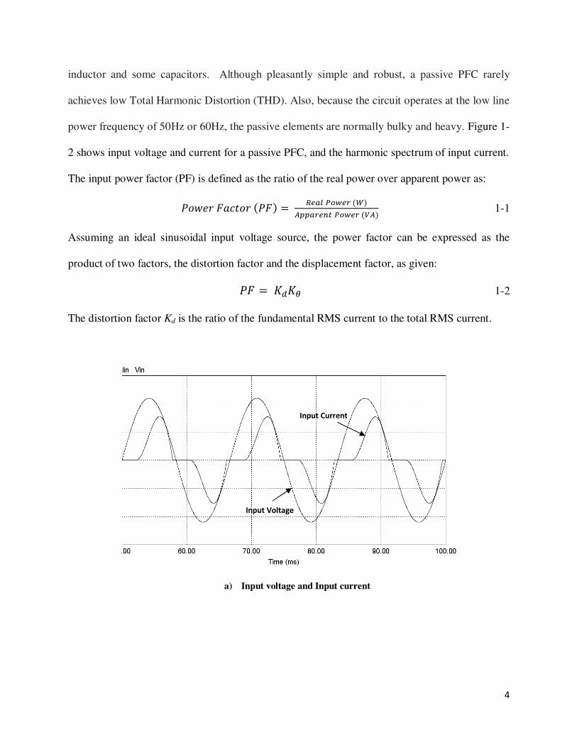
4
inductor and some capacitors. Although pleasantly simple and robust, a passive PFC rarely
achieves low Total Harmonic Distortion (THD). Also, because the circuit operates at the low line
power frequency of 50Hz or 60Hz, the passive elements are normally bulky and heavy. Figure 1-
2 shows input voltage and current for a passive PFC, and the harmonic spectrum of input current.
The input power factor (PF) is defined as the ratio of the real power over apparent power as:
1-1
Assuming an ideal sinusoidal input voltage source, the power factor can be expressed as the
product of two factors, the distortion factor and the displacement factor, as given:
1-2
The distortion factor Kd is the ratio of the fundamental RMS current to the total RMS current.
a) Input voltage and Input current
Input Voltage
Input Current
5
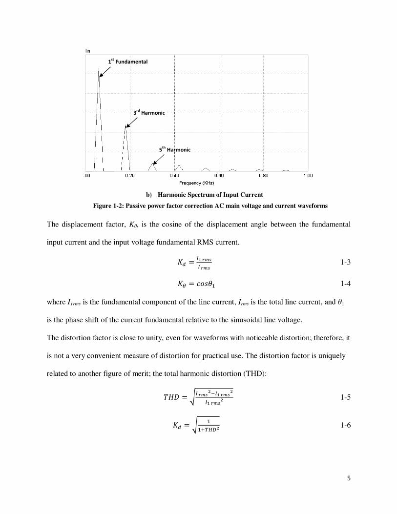
b) Harmonic Spectrum of Input Current
Figure 1-2: Passive power factor correction AC main voltage and current waveforms
The displacement factor, Kθ, is the cosine of the displacement angle between the fundamental
input current and the input voltage fundamental RMS current.
!"# !"# 1-3
$%& 1-4
where I1rms is the fundamental component of the line current, Irms is the total line current, and θ1
is the phase shift of the current fundamental relative to the sinusoidal line voltage.
The distortion factor is close to unity, even for waveforms with noticeable distortion; therefore, it
is not a very convenient measure of distortion for practical use. The distortion factor is uniquely
related to another figure of merit; the total harmonic distortion (THD):
'() * !"#+, !"#+ !"#+ 1-5
* &&-./0+ 1-6
3rd
Harmonic
1st
Fundamental
5th
Harmonic
6
Kd is regulated by IEC 1000-3-2 [2] for lower power levels and by IEEE Std 519-1992 [11] for
higher power levels, where Kθ is regulated by utility companies [12].
Significant reduction of current harmonics in single-phase circuits can only be achieved
by using rectifiers based on pulse width modulated (PWM) switching converters. These
converters can be designed to emulate a resistive load and, therefore, produce very little
distortion of the current. By using PWM or other modulation techniques, these converters draw a
nearly sinusoidal current from the ac line in phase with the line voltage. As a result, the rectifier
operates with very low current harmonic distortion and very high, practically unity power factor.
This technique is commonly known as power factor correction (PFC). As a result of this
research, the existing PFC technology based on the boost converter topology with average-
current-mode control was significantly improved. The proposed improvements allowed an
extended range of operating conditions and additional functionality.
1.3. Literature Review
All basic power converter topologies, such as boost, buck [13], buck-boost, and their
variations, can be used to realize active PFC techniques [14, 15]. At lower power ratings,
MOSFETs [16] are the switching power devices of choice because of their low conduction losses
and high switching speed. For medium and high-power applications, IGBTs can be used in
PWM-controlled converters with switching frequency of up to 30 kHz. There are many
integrated circuits (ICs) [17] on the market that incorporate control functions for PFC converters
and facilitate compact and cost-effective designs. Digital signal processors (DSPs) [18-21] and
microcontrollers [22] have been successfully used to control PFC converters. Microcontrollers
and DSPs can be used to realize traditional [23, 24] proportional-integral derivative (PID) control
laws as well as non-traditional control principles, such as sliding mode control [25], fuzzy logic
7
[26], and neural networks [27]. One of the drawbacks of using microcontrollers and DSPs is the
significant effort that goes into software development.
The boost topology is by far the most popular topology in PFC applications. The boost PFC
converter draws a continuous current from the line and, therefore, does not require much
filtering, which is usually accomplished by an input filter capacitor. Other topologies such as
buck, buck-boost, and flyback draw pulsed current and need a much better input filter. Unlike the
buck topology, the boost converter easily accommodates the input voltage range, from zero to
the line peak voltage.
The boost converter can operate in continuous conduction mode (CCM) [28], discontinuous
conduction mode (DCM), or critical conduction mode (CRM). These names refer to the
continuity of the inductor current within the switching cycle [29]. The boost converter operating
in DCM and CRM modes is usually easier to control, but it has higher peak-to-peak current
ripple, which causes higher RMS value of the inductor current, higher magnetic and conduction
losses, and higher switching noise, which leads to increased filtering requirements. Therefore,
these modes are restricted to relatively low power levels, while the CCM is used at medium and
high power levels.
While the discontinuous conduction mode (DCM) converters such as boost and flyback
converters are well suited for low power applications, continuous conduction mode (CCM) boost
converters with average current mode [30], peak current mode [31] or hysteresis control [32] are
commonly chosen for many medium and high power applications. The output voltage of the
boost PFC converter should be always higher than the peak line voltage. For universal line
application (85 V-265 V), the output voltage is usually set around 400 VDC [33].

8
The boost circuit-based PFC topology operated in CCM is employed in this study as the main
candidate for front end single-phase solutions for AC-DC power factor corrected converters used
in PHEV battery chargers.
1.3.1. Conventional PFC Boost Converter
The conventional boost topology is the most popular topology for PFC applications. It
uses a dedicated diode bridge to rectify the AC input voltage to DC, which is then followed by
the boost section, as shown in Figure 1-3.
Figure 1-3: Conventional PFC boost converter
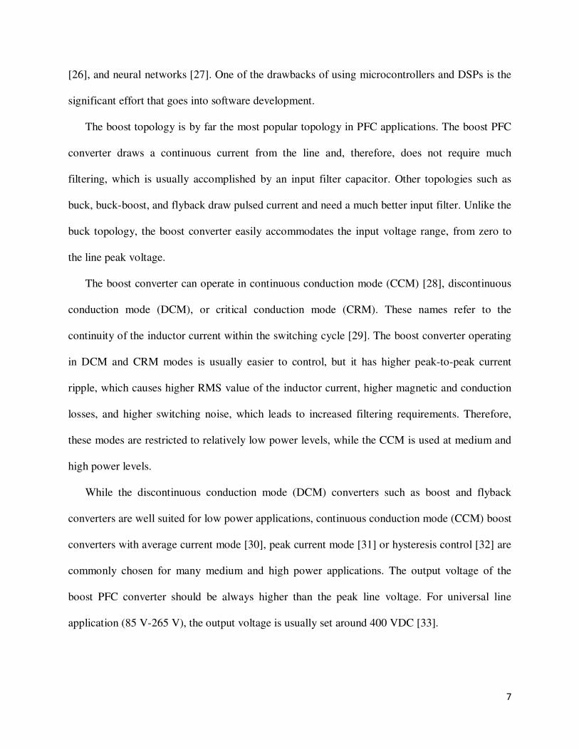
The simplified block diagram of the boost PFC circuit is shown in Figure 1-4 [34]. This circuit
has two control loops: One is the fast acting internal current loop. It defines the input current
shape to be sinusoidal and forces it in phase with the input voltage. The other is the external slow
voltage loop which regulates the output dc voltage. The voltage loop should not react to the
120Hz rectified mains variations, so its bandwidth is between 10 to 20 Hz. The current loop
usually has a bandwidth frequency of less than one tenth of the switching frequency.
9
D1
D3 D4
D2
QB
LB DB
Co
Vin
RL
Rs
Rvi
Rvd
PWM
Drive
Multiplier
Power StageAC Source & RectifierOutput Filter, Load &
Voltage Divider
Full wave
Rectified AC
Input Sensing
Current
Sensing Output
Voltage
SensingVoltage
Error
Vref
Figure 1-4: Simplified block diagram of the boost PFC circuit
The principle operation of boost PFC is as follows: The rectified sinusoidal input voltage
goes to a multiplier circuit, providing a current reference to the multiplier and a feedforward
signal proportional to the RMS value of the line voltage. The filtered dc output voltage of the
boost PFC is compared to a reference voltage, Vref and amplified. The error amplifier senses the
variations between the output voltage and the fixed dc reference voltage. The error signal is then
applied to the multiplier. The multiplier's output follows the shape of the input ac voltage, with
an average value inversely proportional to the RMS value of the ac input voltage. This signal is
compared to the current signal sensed by Rs in a pulse-width modulation (PWM) circuit. The
inductor current waveform follows the shape of the rectified ac line voltage. The gate drive
signal controls the inductor current amplitude and maintains a constant output voltage.
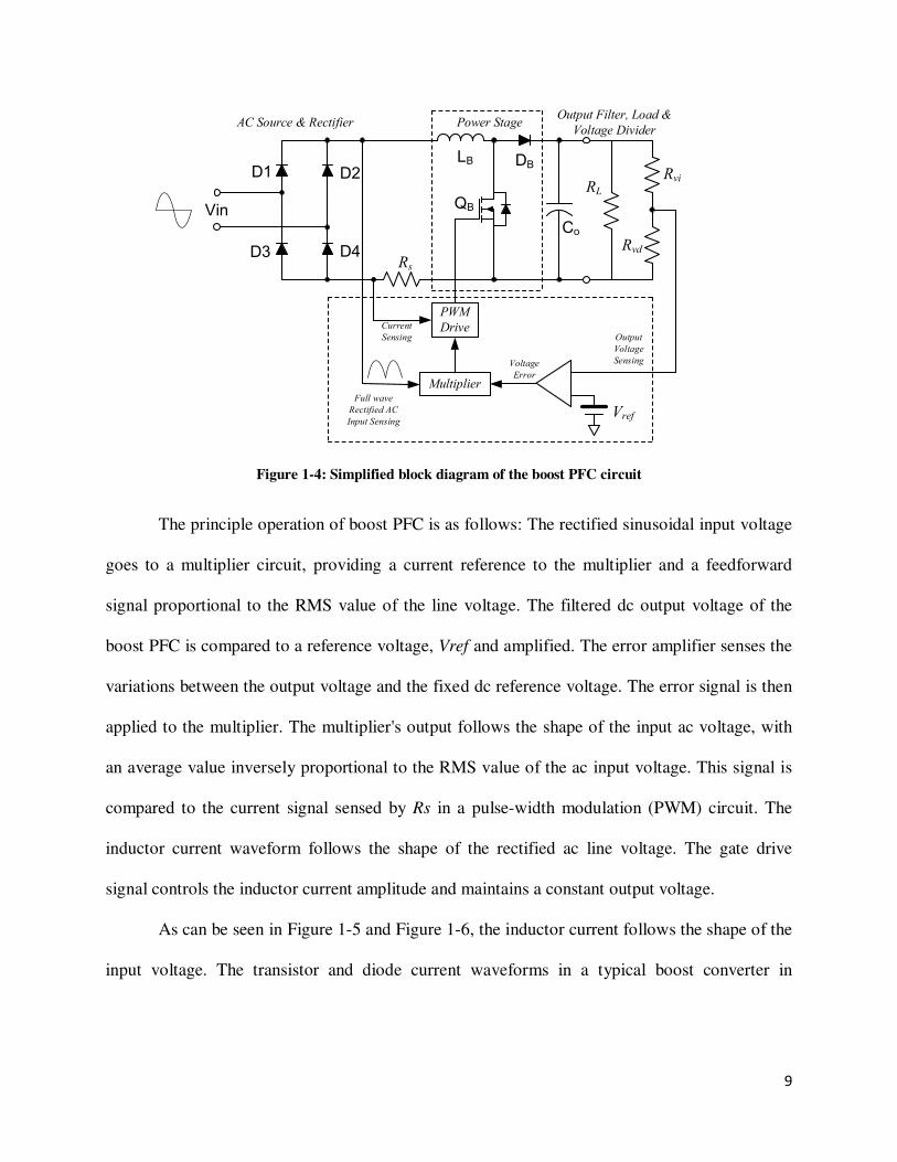
As can be seen in Figure 1-5 and Figure 1-6, the inductor current follows the shape of the
input voltage. The transistor and diode current waveforms in a typical boost converter in
10
continuous conduction mode of operation are pulsed-width modulated, with both the duty cycle
and the peak amplitude varying with the ac input voltage.
Figure 1-5: Inductor current and the duty cycle in a typical PFC boost converter in CCM
Figure 1-6: Top: Transistor current - Bottom: Diode current in a typical PFC boost converter in CCM
The inductor ripple current is directly seen at the converter’s input and will require
filtering to meet EMI specifications [35-46]. The diode output current is discontinuous and needs
Boost Converter
Duty Cycle
Boost Converter
Inductor Current
Boost Transistor
Current
Boost Diode
Current

11
to be filtered out by the output capacitor Co. In this topology, the output capacitor ripple current
is very high and its value is the difference between diode current and the dc output current [47].
In practical applications as the power level increases, the diode bridge losses become
significant, so dealing with heat dissipation in a limited surface area is important, particularly
from an efficiency point of view. Therefore, the conventional PFC boost is limited to a low to a
medium power range (e.g. less than 1000 W).
1.3.2. Bridgeless PFC Boost Converter
The bridgeless PFC (BL PFC) boost converter avoids the need for the rectifier input bridge
yet maintains the classic boost topology, as shown in Figure 1-7 [48-57]. As it is demonstrated in
the following, BL PFC does not have any advantages over conventional PFC in terms of passive
components sizing. However, it eliminates the input bridge rectifiers, so it is an attractive
solution for higher power applications, where the dissipating power in a small area is becoming
extremely difficult and overall efficiency is very important.
Figure 1-7: Bridgeless PFC boost topology
The intrinsic body diode connected between the drain and source of the Power MOSFET
switches has an important role in this topology. The circuit shown from a functional point of
view is similar to the common boost converter. In the traditional topology current flows through

12
two of the bridge diodes in series. In the bridgeless PFC configuration, current flows through
only one diode with the Power MOSFET providing the return path. To analyze the circuit
operation, it is necessary to separate it into two sections. The first section operates as the boost
stage and the second section operates as the return path for the AC input signal.
1.3.2.1. Positive "HALF Cycle" Operation
When the AC input voltage goes positive, the gate of Q1 is driven high and current flows
from the input through the inductors, storing energy in L1 and L2 as shown in Figure 1-8-a).
When Q1 turns off, energy in the inductors is released as current flows through D1, through the
load and returns through the body diode of Q2 back to the input mains. During the-off time, the
current through the inductors (which during this time discharges its energy) flows into the boost
diode D1 and close the circuit through the load.
1.3.2.2. Negative "HALF Cycle" Operation
During the negative half cycle circuit operation is mirrored. Q2 turns on, current flows
through the inductor, storing energy, as shown in Figure 1-8-b). When Q2 turns off, energy is
released as current flows through D2, through the load, and back to the mains through the body
diode of Q1.
a) Positive half cycle

13
b) Negative half cycle
Figure 1-8: Bridgeless PFC converter operation
Note that the two Power MOSFETs are driven synchronously. It doesn't matter whether
the sections are performing as an active boost or as a path for the current to return. In either case
there is a benefit of lower power dissipation when current flows through the Power MOSFETs
(through intrinsic body diodes) during the return phase.
As can be noted, in bridgeless topology a new loss has been introduced in the intrinsic
body diodes of MOSFETs and it might add extra power dissipation in the MOSFETs, but since
input bridge rectifiers were eliminated, there is some efficiency gain in overall performance of
the bridgeless topology.
For a conventional PFC, the current sense is easy to monitor by simply inserting a shunt
sensing resistor at the return path of the inductor current. However, for a bridgeless PFC, current
path does not share the same ground at each half-line cycle. A sensing-power MOSFET and
diode current are needed, which makes the bridgeless PFC’s current sensing complicated and
difficult to monitor [52, 58].
In addition, since the AC line is floating compared to the PFC stage ground, simple
circuitry cannot sense input voltage. Normally a low-frequency transformer or optical coupler is
required to perform input voltage sensing.
14
1.3.2.1. PSIM Simulation of Bridgeless Boost Converter
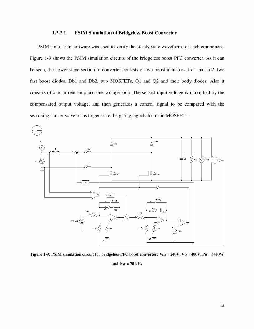
PSIM simulation software was used to verify the steady state waveforms of each component.
Figure 1-9 shows the PSIM simulation circuits of the bridgeless boost PFC converter. As it can
be seen, the power stage section of converter consists of two boost inductors, Ld1 and Ld2, two
fast boost diodes, Db1 and Db2, two MOSFETs, Q1 and Q2 and their body diodes. Also it
consists of one current loop and one voltage loop. The sensed input voltage is multiplied by the
compensated output voltage, and then generates a control signal to be compared with the
switching carrier waveforms to generate the gating signals for main MOSFETs.
Figure 1-9: PSIM simulation circuit for bridgeless PFC boost converter: Vin = 240V, Vo = 400V, Po = 3400W
and fsw = 70 kHz
15
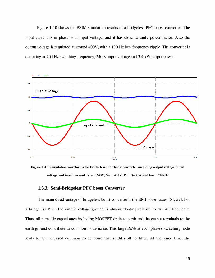
Figure 1-10 shows the PSIM simulation results of a bridgeless PFC boost converter. The
input current is in phase with input voltage, and it has close to unity power factor. Also the
output voltage is regulated at around 400V, with a 120 Hz low frequency ripple. The converter is
operating at 70 kHz switching frequency, 240 V input voltage and 3.4 kW output power.
Figure 1-10: Simulation waveforms for bridgeless PFC boost converter including output voltage, input
voltage and input current: Vin = 240V, Vo = 400V, Po = 3400W and fsw = 70 kHz
1.3.3. Semi-Bridgeless PFC boost Converter
The main disadvantage of bridgeless boost converter is the EMI noise issues [54, 59]. For
a bridgeless PFC, the output voltage ground is always floating relative to the AC line input.
Thus, all parasitic capacitance including MOSFET drain to earth and the output terminals to the
earth ground contribute to common mode noise. This large dv/dt at each phase's switching node
leads to an increased common mode noise that is difficult to filter. At the same time, the

16
switching node Q2 and D2 are directly connected to input line terminal, which leads to high
dv/dt common mode noise.
The semi-bridgeless PFC boost converter is proposed [60] to address the EMI noise issues
for BL PFC Converters by adding two slow diodes, Da and Db to the input line as shown in
Figure 1-11. The added diodes have no effect on the efficiency of converter since they are in
parallel with another semiconductor when they conduct. As a matter of fact, they will reduce the
current stress on the min MOSFET in BL PFC configuration.
Figure 1-11: Bridgeless PFC boost topology
1.3.4. Interleaved PFC Boost Converter
The interleaved PFC boost converter (IL PFC) illustrated in Figure 1-12 is simply two
boost converters in parallel operating 180° out of phase. The input current is the sum of the two
inductor currents IL1 and IL2. Because the inductor’s ripple currents are out of phase, they tend to
cancel each other and reduce the input ripple current caused by the boost inductors [61-67].
The maximum input inductor ripple current cancellation occurs at 50% duty cycle. The output
capacitor current is the sum of the two boost diode currents less the dc output current.
Interleaving reduces the output capacitor ripple current as a function of the duty cycle [64]. As
the duty cycle approaches 0%, 50%, and 100% duty cycle, the sum of the two diode currents
approaches dc. At these points, the output capacitor only has to filter the inductor ripple current.
17
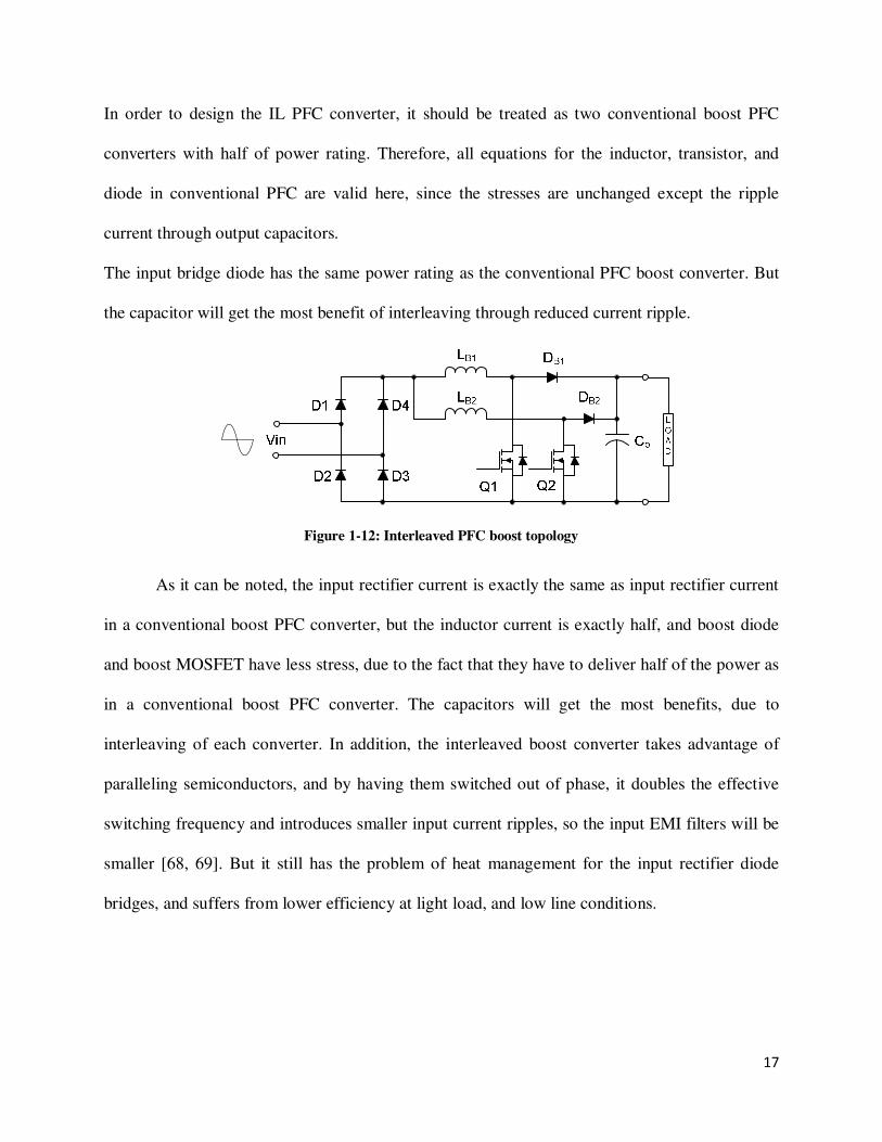
In order to design the IL PFC converter, it should be treated as two conventional boost PFC
converters with half of power rating. Therefore, all equations for the inductor, transistor, and
diode in conventional PFC are valid here, since the stresses are unchanged except the ripple
current through output capacitors.
The input bridge diode has the same power rating as the conventional PFC boost converter. But
the capacitor will get the most benefit of interleaving through reduced current ripple.
Figure 1-12: Interleaved PFC boost topology
As it can be noted, the input rectifier current is exactly the same as input rectifier current
in a conventional boost PFC converter, but the inductor current is exactly half, and boost diode
and boost MOSFET have less stress, due to the fact that they have to deliver half of the power as
in a conventional boost PFC converter. The capacitors will get the most benefits, due to
interleaving of each converter. In addition, the interleaved boost converter takes advantage of
paralleling semiconductors, and by having them switched out of phase, it doubles the effective
switching frequency and introduces smaller input current ripples, so the input EMI filters will be
smaller [68, 69]. But it still has the problem of heat management for the input rectifier diode
bridges, and suffers from lower efficiency at light load, and low line conditions.
18
1.3.4.1. PSIM Simulation of Interleaved Boost Converter
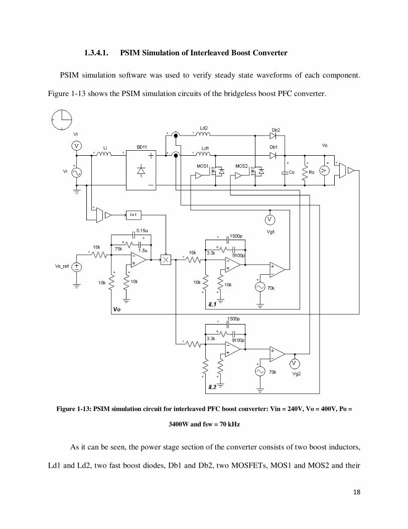
PSIM simulation software was used to verify steady state waveforms of each component.
Figure 1-13 shows the PSIM simulation circuits of the bridgeless boost PFC converter.
Figure 1-13: PSIM simulation circuit for interleaved PFC boost converter: Vin = 240V, Vo = 400V, Po =
3400W and fsw = 70 kHz
As it can be seen, the power stage section of the converter consists of two boost inductors,
Ld1 and Ld2, two fast boost diodes, Db1 and Db2, two MOSFETs, MOS1 and MOS2 and their
19
body diodes. Also it consists of two current loops and one voltage loop. The sensed input voltage
is multiplied by the compensated output voltage, and then generates a control signal to be
compared with the switching carrier waveforms to generate the gating signals for main
MOSFETs.
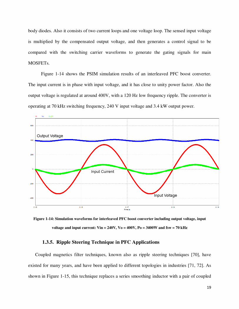
Figure 1-14 shows the PSIM simulation results of an interleaved PFC boost converter.
The input current is in phase with input voltage, and it has close to unity power factor. Also the
output voltage is regulated at around 400V, with a 120 Hz low frequency ripple. The converter is
operating at 70 kHz switching frequency, 240 V input voltage and 3.4 kW output power.
Figure 1-14: Simulation waveforms for interleaved PFC boost converter including output voltage, input
voltage and input current: Vin = 240V, Vo = 400V, Po = 3400W and fsw = 70 kHz
1.3.5. Ripple Steering Technique in PFC Applications
Coupled magnetics filter techniques, known also as ripple steering techniques [70], have
existed for many years, and have been applied to different topologies in industries [71, 72]. As
shown in Figure 1-15, this technique replaces a series smoothing inductor with a pair of coupled
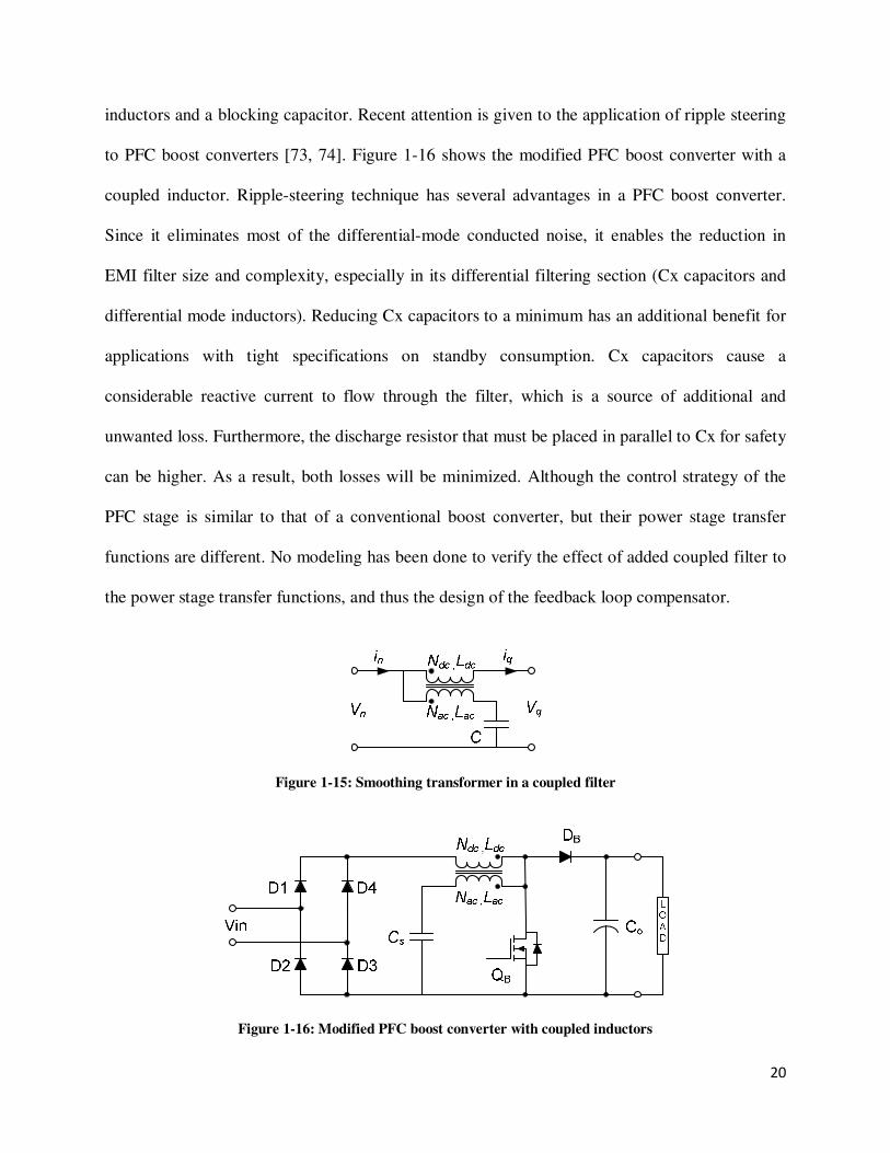
20
inductors and a blocking capacitor. Recent attention is given to the application of ripple steering
to PFC boost converters [73, 74]. Figure 1-16 shows the modified PFC boost converter with a
coupled inductor. Ripple-steering technique has several advantages in a PFC boost converter.
Since it eliminates most of the differential-mode conducted noise, it enables the reduction in
EMI filter size and complexity, especially in its differential filtering section (Cx capacitors and
differential mode inductors). Reducing Cx capacitors to a minimum has an additional benefit for
applications with tight specifications on standby consumption. Cx capacitors cause a
considerable reactive current to flow through the filter, which is a source of additional and
unwanted loss. Furthermore, the discharge resistor that must be placed in parallel to Cx for safety
can be higher. As a result, both losses will be minimized. Although the control strategy of the
PFC stage is similar to that of a conventional boost converter, but their power stage transfer
functions are different. No modeling has been done to verify the effect of added coupled filter to
the power stage transfer functions, and thus the design of the feedback loop compensator.
Figure 1-15: Smoothing transformer in a coupled filter
Figure 1-16: Modified PFC boost converter with coupled inductors

21
Replacing the inductor in a conventional boost converter shown in Figure 1-3 with the
coupled inductor and a blocking capacitor shown in Figure 1-15 will result to the modified boost
converter with coupled magnetic shown in Figure 1-16.
1.3.6. Average Switch Model
Models for the PWM-switch were first introduced in [75, 76]. It was then adopted for
different converters in [77-81]. For the average switch model of a converter, the active and
passive switches shown in Figure 1-17 are replaced with the PWM-switch equivalent circuits
shown in Figure 1-18 and Figure 1-19.
Figure 1-17: One active switch and one passive switch
Figure 1-18: PWM-switch
Figure 1-19: Averaged model of PWM-switch

22
Using this model and applying that to modified boost converter with coupled inductors,
any of the transfer functions between the output variables (output voltage and inductor current)
and the input variables (input voltage and duty ration) can be derived.
1.4. Motivation and Objectives of the Thesis
The objective of this thesis is to investigate and conduct research on the high-
performance single-phase solutions for AC-DC power factor corrected converters for plug-in
hybrid electric vehicle battery chargers.
A variety of circuit topologies and control methods have been developed for PFC
applications. The two-stage approach is the proper candidate for PHEV battery chargers, where
the power rating is relatively high, and lithium-ion batteries are used as the main energy storage
system. The improvement of overall charger efficiency is critical for the emergence and
acceptance of these vehicular technologies, as the charger efficiency increases, the charge time
and utility cost decreases. Additionally, to meet the efficiency and power factor requirements and
regulatory standards for the AC supply mains, power factor correction is essential.
Due to limited space in vehicle and increasing power consumption, chargers are required
to deliver more power with smaller volume. As a key component of a charger system, the front-
end AC/DC converter must achieve high efficiency and power density. In this dissertation,
several conventional plug in hybrid electric vehicle charger front end AC-DC converter
topologies are investigated and a new bridgeless interleaved and a phase shifted semi-bridgeless
power factor corrected converter are proposed to improve the efficiency and performance, which
is critical to minimize the charger size, charging time and the amount and cost of electricity
drawn from the utility.
23
1.5. Outline of the Thesis
This thesis consists of five chapters. Chapter 1 introduces the subject of AC-DC power
factor corrected boost converters with particular focus on its application for plug-in hybrid
electric vehicles. This chapter establishes motivation and sets objectives for the research
contributions presented in Chapters 2-5. A literature review on existing topologies -
conventional boost converter, bridgeless boost converter and interleaved boost converter - modes
of operation, control techniques and PSIM simulation of existing topologies are presented in
Chapter 1. Chapter 2 proposes a new bridgeless interleaved PFC boost converter for PHEV
battery charger applications. The circuit description and steady state analysis, semiconductor
loss analysis, design procedure, logic implementation, PSIM simulation and experimental results
are presented. Chapter 3 introduces a new phase shifted semi-bridgeless PFC boost converter for
PHEV battery charger applications. The circuit description and steady state analysis,
semiconductor loss analysis, design procedure, logic implementation, PSIM simulation and
experimental results are presented. A new average switch modeling for ripple steering technique
applied to PFC boost converters and compensation network design based on derived voltage and
current power stage transfer functions are presented in Chapter 4. Simulation and experimental
results are presented to verify the model. Chapter 5 summarizes the contributions of the research
presented in this thesis and gives recommendations for future work.

24
CHAPTER 2. Bridgeless Interleaved PFC Boost Converter
2.1. Introduction
In this chapter, a new bridgeless interleaved power factor corrected converter for plug in
hybrid electric vehicle charger front end AC-DC converter topology is investigated and proposed
to improve the efficiency and performance, which is critical to minimize the charger size,
charging time, and the amount and the cost of electricity drawn from the utility. A detailed
analytical model for this topology is developed, enabling the calculation of power losses and
efficiency. Experimental and simulation results of a prototype boost converter converting
universal AC input voltage to 400 V DC at 3.4 kW are given to verify the proof of concept, and
analytical work reported in this chapter. The results show a power factor of greater than 0.99
from 750 W to 3.4 kW, THD less than 5% from half load to full load, and a peak efficiency of
98.94 % at 265 V input, and 1.2 kW output power.
2.2. Circuit Description and Steady State Analysis
The bridgeless interleaved (BLIL) PFC converter [82] shown in Figure 2-1 is proposed to
address the problems discussed in Chapter 1 for the conventional boost, bridgeless boost, and
interleaved boost topologies. This converter introduces two more MOSFETs and two more fast
diodes in place of four slow diodes used in the input bridge of the benchmark interleaved boost
PFC converter. To analyze the circuit operation, the input line cycle has been separated into the
positive and negative half cycles, as explained in sub-sections that follow. In addition, the
detailed circuit operation depends on the duty cycle, therefore positive half cycle operation
analysis is provided for D > 0.5 and D < 0.5.

25
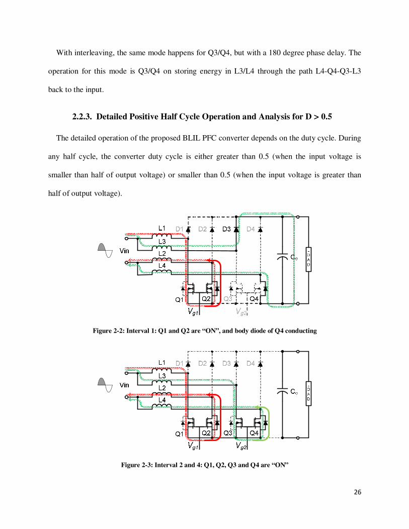
Figure 2-1: Proposed bridgeless interleaved (BLIL) PFC boost converter
2.2.1. Positive Half Cycle Operation
Referring to Figure 2-1, during the positive half cycle, when the AC input voltage is positive,
Q1/Q2 turn on and current flows through L1 and Q1 and continues through Q2 and then L2,
returning to the line while storing energy in L1 and L2. When Q1/Q2 turn off, energy stored in
L1 and L2 is released as current flows through D1, through the load and returns through the body
diode of Q2 back to the input mains.
With interleaving, the same mode happens for Q3/Q4, but with a 180 degree phase delay.
The operation for this mode is Q3/Q4 on storing energy in L3/L4 through the path L3-Q3-Q4-L4
back to the input. When Q3/Q4 turn off, energy is released through D3 to the load and returning
through the body diode of Q4 back to the input mains.
2.2.2. Negative Half Cycle Operation
Referring to Figure 2-1, during the negative half cycle, when the AC input voltage is negative,
Q1/Q2 turn on and current flows through L2 and Q2 and continues through Q1 and then L1,
returning to the line while storing energy in L2 and L1. When Q1/Q2 turn off, energy stored in
L2 and L1 is released as current flows through D2, through the load and returns through the body
diode of Q1 back to the input mains.
26
With interleaving, the same mode happens for Q3/Q4, but with a 180 degree phase delay. The
operation for this mode is Q3/Q4 on storing energy in L3/L4 through the path L4-Q4-Q3-L3
back to the input.
2.2.3. Detailed Positive Half Cycle Operation and Analysis for D > 0.5
The detailed operation of the proposed BLIL PFC converter depends on the duty cycle. During
any half cycle, the converter duty cycle is either greater than 0.5 (when the input voltage is
smaller than half of output voltage) or smaller than 0.5 (when the input voltage is greater than
half of output voltage).
Figure 2-2: Interval 1: Q1 and Q2 are “ON”, and body diode of Q4 conducting
Figure 2-3: Interval 2 and 4: Q1, Q2, Q3 and Q4 are “ON”
27
Figure 2-4: Interval 3: Q3 and Q4 are “ON”, and body diode of Q2 conducting
Figures 2-2 to 2-4 show the three unique operating interval circuits of the proposed converter
for duty cycles greater than 0.5 during positive half cycle operation. Waveforms of the proposed
converter during these conditions are shown in Figure 2-5.
Since the switching frequency of proposed converter is much higher than the frequency of input
line voltage, the input voltage v2 is considered constant during one switching period T4. The
input voltage is given by:
56 √2 9:$;< % 2-1 In a positive half cycle of the input voltage, the duty ratio of the proposed converter determines
the following voltage relation:
=>? &&,0 2-2 The intervals of operation are explained as follows. In addition, the ripple current components
are derived, enabling calculation of the input ripple current, which provides design guidance to
meet the required input current ripple standard.
Interval 1 [t0-t1]: At t0, Q1/ Q2 are ON, and Q3/Q4 are off, as shown in Figure 2-2. During
this interval, the current in series inductances L1 and L2 increases linearly and stores the energy
in these inductors. The ripple currents in Q1 and Q2 are the same as the current in series

28
inductances L1 and L2, where the ripple current is given by:
Figure 2-5: BLIL PFC boost converter steady-state waveforms at D > 0.5

29
∆;A& &A -A+ 561 − )': 2-3 The current in series inductances L3 and L4 decreases linearly and transfers the energy to the
load through D3, Co and body diode of Q4. The ripple current in series inductances L3 and L4
is given by:
∆;AD &AE-AF 9 − 561 − )': 2-4 The input ripple current is the sum of currents in L1/L2 and L3/L4:
∆G6 &A -A+ 9 1 − )': 2-5 Interval 2 [t1-t2]: At t1, Q3/Q4 are turned on, while Q1/Q2 remain on, as shown in Figure
2-3. During this interval, the current in the four inductors each increase linearly, storing energy
in these inductors. The ripple currents in Q1 and Q2 are the same as the ripple current in series
inductances L1 and L2 as given by:
∆;A& &A -A+ 56) − &H': 2-6 Similarly, the ripple currents in Q3 and Q4 are the same as the ripple current in series
inductances L3 and L4:
∆;AD &AE-AF 56) − &H': 2-7 The input ripple current is the sum of currents in L1/L2 and L3/L4:
∆G6 HA -A+ 56) − &H': 2-8 Interval 3 [t2-t3]: At t2, Q1/Q2 are turned off, while Q3/ Q4 remain on, as shown in
Figure 2-4. During this interval, the current in series inductances L3 and L4 increases linearly
and stores the energy in these inductors. The ripple currents in Q3 and Q4 are the same as the
ripple current in series inductances L3 and L4:

30
∆;AD &AE-AF 561 − )': 2-9 The current in L1 and L2 decreases linearly and transfers the energy to the load through D1, Co
and body diode of Q2. The ripple current in series inductances L1 and L2 is given by:
∆;A& &A -A+ 9 − 561 − )': 2-10 The input ripple current is the sum of currents in L1/L2 and L3/L4:
∆G6 &A -A+ 9 1 − )': 2-11 Interval 4 [t3-t4]: At t3, Q3/Q4 remain on, while Q1/Q2 are turned on, as shown in Figure
2-3. During this interval, the currents in the four inductors each increase linearly, storing energy
in these inductors. The ripple currents in Q1 and Q2 are the same as the ripple currents in L1/L2:
∆;A& &A -A+ 56) − &H': 2-12 Similarly, the ripple currents Q3 and Q4 are the same as the ripple current in series inductances
L3 and L4:
∆;AD &AE-AF 56) − &H': 2-13 The input ripple current is the sum of currents in L1/L2 and L3/L4:
∆G6 HA -A+ 56) − &H': 2-14 2.2.4. Detailed Positive Half Cycle Operation and Analysis for D < 0.5
Figure 2-6 to Figure 2-8 show the operating interval circuits of the proposed converter for duty
cycles smaller than 0.5 during the positive half cycle. The waveforms of the proposed converter
during these conditions are shown in Figure 2-9. The intervals of operation are explained as
follows:
31
D1L1 D2 D3 D4
Q1 Q2 Q3 Q4
L3
L2
L4
Co
L
O
A
D
Vin
Vg1 Vg2
Figure 2-6: Interval 1 and 3: Body diodes of Q2 and Q4 conducting
Figure 2-7: Interval 2: Q1 and Q2 are “ON”, and body diode of Q4 conducting
Figure 2-8: Interval 4: Q3 and Q4 are “ON”, and body diode of Q2 conducting

32
Interval 1 [t0-t1]: At t0, Q1 and Q2 turn off, while Q3 and Q4 remain off, as shown in
Figure 2-6. During this interval, the current in series inductances L1 and L2 decreases linearly
and transfers the energy to the load through D1, Co and body diode of Q2. The ripple current in
series inductances L1 and L2 is:
∆;A& &A -A+ 9 − 56&H − )': 2-15 In addition, the current in the series inductances L3 and L4 also decreases linearly, transferring
the energy to the load through D3, Co and body diode of Q4. The ripple current in series
inductances L3 and L4 is:
∆;AD &AE-AF 9 − 56&H − )': 2-16 The input current is the sum of currents in L1/L2 and L3/L4:
∆G6 HA -A+ 9 − 56&H − )': 2-17 Interval 2 [t1-t2]: At t1, Q1/Q2 turn on, while Q3/Q4 remain off, as shown in Figure 2-7.
During this interval, the current in series inductances L1 and L2 increases linearly, storing
energy in these inductors. The ripple currents in Q1 and Q2 are the same as the current in series
inductances L1 and L2, where the ripple current is given by:
∆;A& &A -A+ 56)': 2-18 The current in series inductances L3 and L4 decreases linearly and transfers the energy to the
load through D3, Co and body diode of Q4. The ripple current in L3 and L4 is:
∆;AD &AE-AF 9 − 56)': 2-19 The input ripple current is the sum of the currents in L1/L2 and L3/L4:
∆G6 &A -A+ 9 )': 2-20

33
t
t
t
t
t
t
Vg2
t
Vg1
Input Current
DTS(1-D)TS
t0 t1 t2 t3 t4 t5
∆Iin
Gating Signals
Inductor Current
FET Current
Boost Diode
Current
Body Diode
Currentt
IL1
IQ1
ID1
IQd3
IL3
IQ3
ID3
IQd1
Figure 2-9: BLIL PFC boost converter steady-state waveforms at D < 0.5

34
Interval 3 [t2-t3]: At t2, Q1/Q2 are turned off, while Q3/Q4 remain off, as shown in
Figure 2-6. During this interval, the current in series inductances L1 and L2 decreases linearly
and transfers the energy to the load through D1, Co and body diode of Q2. The ripple current in
series inductances L1 and L2 is given by:
∆;A& &A -A+ 9 − 56&H − )': 2-21
Similarly, the current in the series inductances L3 and L4 also decreases linearly, transferring the
energy to the load through D3, Co and body diode of Q4. The ripple current in series inductances
L3 and L4 is:
∆;AD &AE-AF 9 − 56&H − )': 2-22
The input current is the sum of currents in L1/L2 and L3/L4:
∆G6 HA -A+ 9 − 56&H − )': 2-23
Interval 4 [t3-t4]: At t3, Q3/Q4 are turned on, while Q1/Q2 remain off, as shown in Figure
2-8. During this interval, the current in series inductances L3 and L4 increases linearly and stores
the energy in these inductors. The ripple currents in Q3 and Q4 are the same as the current in
series inductances L3 and L4, where the ripple current is given by:
∆;AD &AE-AF 56)': 2-24
The current in series inductances L1 and L2 decreases linearly and transfers the energy to the
load through D2, Co and body diode of Q4. The ripple current in L1 and L2 is:
∆;A& &A -A+ 9 − 56)': 2-25
The input ripple current is the sum of currents in L1/L2 and L3/L4:
∆G6 &A -A+ 9 )': 2-26

35
The operation of converter during the negative input voltage half cycle is similar to the operation
of converter during the positive input voltage half cycle.
2.3. Loss Modeling
In order to properly select the power stage components of a converter and calculate the
associated power losses, it is necessary to determine the RMS and the average values of their
currents [83]. In a typical boost converter, the MOSFET and diode current waveforms are
pulsed-width modulated, with both the duty cycle and peak amplitude varying with the AC input.
Without an effective mathematical method for computing these RMS and average values, the
proper design and selection of power stage components can be flawed. The following
assumptions were made in order to analyze the converters and to derive the stress equations:
a) These calculations are based on CCM operation of the PFC boost converter.
b) Assuming unity power factor, the line current is in phase and shape with the input line
voltage – a sinusoidal waveform.
c) The PFC output voltage is DC with no voltage ripple.
In a typical boost converter, the converter MOSFET duty cycle is given by:
IJ% 1 − |?L|= 1 − MN|:6 | = 2-27 Therefore
IJ,O: *&P Q R1 − MN|:6 | = SHPT U% 2-28 Assuming the inductor current is a sinusoidal waveform:
;A % GV|$;< %| 2-29 The instantaneous MOSFET current and its RMS current can be derived respectively:
;J% GV|$;<%|. IJ,O: 2-30

36
GJ,O: *&P Q RGV|$;<%|1 − MN|:6 |= SHPT U% 2-31 The inductor current ripple is assumed to be half of peak inductor current:
∆G &H MNH 2-32 The high frequency ripple components of inductor current is assumed to be a triangular
waveform with a fixed duty cycle, so the RMS current in each inductor is defined by:
GA,O: * &√H MNH H + &H√D ∆G H YZ√D ?LMN 2-33 The boost diode duty cycle is given by:
I0% 1 − IJ% MN|:6 |= 2-34 Therefore the instantaneous boost diode current and its RMS current can be derived respectively:
;0% GV|$;<%| MN|:6 |= 2-35 G0,O: *&P Q RGV|$;<%|MN|:6 |= SHPT U% 2-36
The output capacitor current has high frequency and low frequency components. The low
frequency component is simply calculated by:
G[,O:A\ =√H √HH == 2-37 The high frequency RMS ripple current component is:
G[,O:/\ ?L= * &] =]P MN − =+?L+ 2-38 The same method was used to derive RMS current in different topologies. Table 2-1
shows a summary of component RMS current stress for conventional boost converter and
bridgeless boost converter. Table 2-2 provides the same summary for interleaved boost converter
and bridgeless interleaved boost converter.
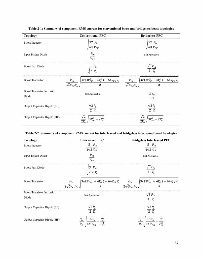
37
Table 2-1: Summary of component RMS current for conventional boost and bridgeless boost topologies
Topology Conventional PFC Bridgeless PFC
Boost Inductor ^9748 69V ^9748 69V
Input Bridge Diode 69V Not Applicable
Boost Fast Diode ^32 69 √32 69
Boost Transistor 6√69V9^3e39VH + 49H − 649V9e
6√69V9^3e39VH + 49H − 649V9e
Boost Transistor Intrinsic
Diode Not Applicable √32 69
Output Capacitor Ripple (LF) √22 9 √22 9
Output Capacitor Ripple (HF) √229 *36H − 2H √229 *36H − 2H
Table 2-2: Summary of component RMS current for interleaved and bridgeless interleaved boost topologies
Topology Interleaved PFC Bridgeless Interleaved PFC
Boost Inductor 54√3 69V 54√3 69V Input Bridge Diode 69V
Not Applicable
Boost Fast Diode ^32 62. 9 √34 69
Boost Transistor 62√69V9^3e39VH + 49H − 649V9e
62√69V9^3e39VH + 49H − 649V9e
Boost Transistor Intrinsic
Diode Not Applicable √34 69
Output Capacitor Ripple (LF) √22 9 √22 9
Output Capacitor Ripple (HF) 69 ^ 16 96e 9V − H6H 69 ^ 16 96e 9V − H6H

38
Table 2-3 shows a summary of component Average current stress for conventional boost
converter and bridgeless boost converter. Table 2-4 provides the same summary for interleaved
boost converter and bridgeless interleaved boost converter.
Table 2-3: Summary of component average current for conventional boost and bridgeless boost topologies
Topology Conventional PFC Bridgeless PFC
Boost Inductor 4e 69V 0
Input Bridge Diode 2e 69V Not Applicable
Boost Fast Diode 69 12 69
Boost Transistor 64e 19V − 19 12 69
Boost Transistor Intrinsic
Diode Not Applicable 12 69
Table 2-4: Summary of component average current for interleaved and bridgeless interleaved boost
topologies
Topology Interleaved PFC Bridgeless Interleaved PFC
Boost Inductor 2e 69V 0 Input Bridge Diode 2e 69V
Not Applicable
Boost Fast Diode 62. 9 14 69
Boost Transistor 64e 19V − 12 19 14 69
Boost Transistor Intrinsic
Diode Not Applicable 14 69
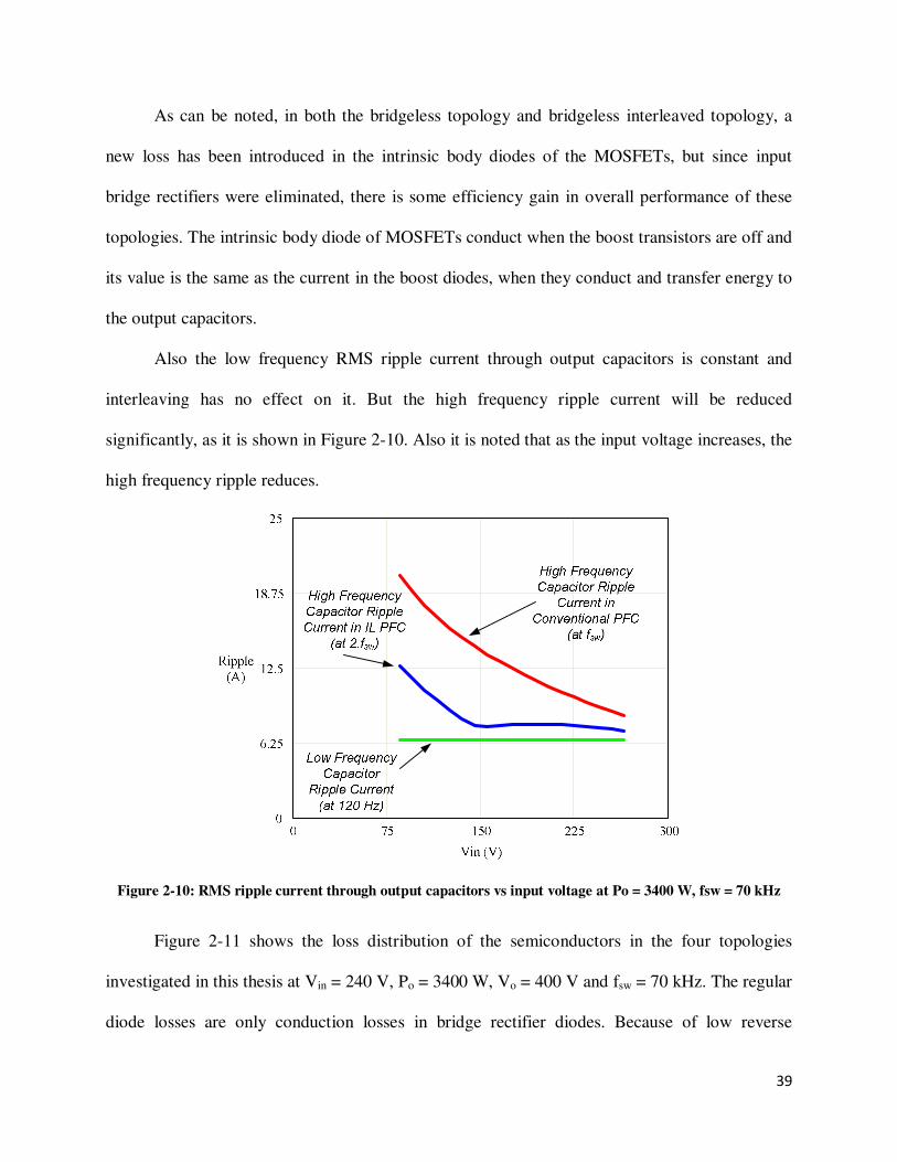
39
As can be noted, in both the bridgeless topology and bridgeless interleaved topology, a
new loss has been introduced in the intrinsic body diodes of the MOSFETs, but since input
bridge rectifiers were eliminated, there is some efficiency gain in overall performance of these
topologies. The intrinsic body diode of MOSFETs conduct when the boost transistors are off and
its value is the same as the current in the boost diodes, when they conduct and transfer energy to
the output capacitors.
Also the low frequency RMS ripple current through output capacitors is constant and
interleaving has no effect on it. But the high frequency ripple current will be reduced
significantly, as it is shown in Figure 2-10. Also it is noted that as the input voltage increases, the
high frequency ripple reduces.
Figure 2-10: RMS ripple current through output capacitors vs input voltage at Po = 3400 W, fsw = 70 kHz
Figure 2-11 shows the loss distribution of the semiconductors in the four topologies
investigated in this thesis at Vin = 240 V, Po = 3400 W, Vo = 400 V and fsw = 70 kHz. The regular
diode losses are only conduction losses in bridge rectifier diodes. Because of low reverse
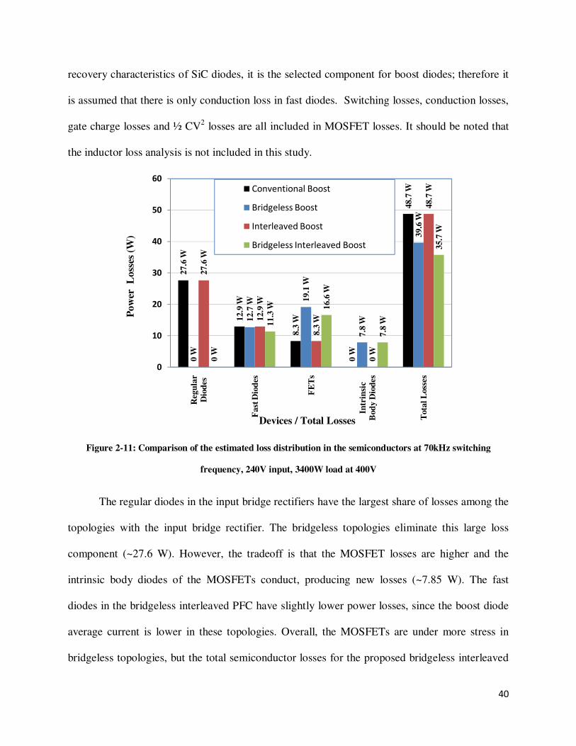
40
recovery characteristics of SiC diodes, it is the selected component for boost diodes; therefore it
is assumed that there is only conduction loss in fast diodes. Switching losses, conduction losses,
gate charge losses and ½ CV2 losses are all included in MOSFET losses. It should be noted that
the inductor loss analysis is not included in this study.
Figure 2-11: Comparison of the estimated loss distribution in the semiconductors at 70kHz switching
frequency, 240V input, 3400W load at 400V
The regular diodes in the input bridge rectifiers have the largest share of losses among the
topologies with the input bridge rectifier. The bridgeless topologies eliminate this large loss
component (~27.6 W). However, the tradeoff is that the MOSFET losses are higher and the
intrinsic body diodes of the MOSFETs conduct, producing new losses (~7.85 W). The fast
diodes in the bridgeless interleaved PFC have slightly lower power losses, since the boost diode
average current is lower in these topologies. Overall, the MOSFETs are under more stress in
bridgeless topologies, but the total semiconductor losses for the proposed bridgeless interleaved
27.6
W
12.9
W
8.3
W
0 W
48.7
W
0 W
12.7
W
19.1
W
7.8
W
39.6
W
27.6
W
12.9
W
8.3
W
0 W
48.7
W
0 W
11.3
W 16.6
W
7.8
W
35.7
W
0
10
20
30
40
50
60
Reg
ula
r
Dio
des
Fast
Dio
des
FE
Ts
Intr
insi
c
Bod
y D
iod
es
Tota
l L
oss
es
Pow
er
Loss
es (
W)
Devices / Total Losses
Conventional Boost
Bridgeless Boost
Interleaved Boost
Bridgeless Interleaved Boost

41
boost are 37% lower than the benchmark conventional boost, 10% lower than the bridgeless
boost and 37% lower than the benchmark interleaved boost.
Since the bridge rectifier losses are so large, it was expected that the bridgeless interleaved
boost converter would have the least power losses among all four introduced topologies. Also it
was noted that the losses in the input bridge rectifiers were 56% of total losses in the
conventional PFC converter and in the benchmark interleaved PFC converter. Therefore
eliminating the input bridges in PFC converters is justified despite the fact that new losses are
introduced.
2.4. Math Modeling Verification
In order to verify the accuracy of converters modeled in section 2.3, the math modeling results
were compared with PSIM simulations for two different topologies. The RMS inductor current,
the RMS MOSFET current, the average boost diode current and the average MOSFET body
diode current for an interleaved boost PFC topology and a bridgeless boost PFC topology were
examined.
Figure 2-12 to Figure 2-14 show the PSIM simulation and Math modeled values of boost
inductor RMS current, MOSFET RMS current and boost diode average current for an interleaved
boost PFC converter at 240 V input and 120 V input voltages.
Figure 2-15 to Figure 2-18 show the PSIM simulation and Math modeled values of boost
inductor RMS current, MOSFET RMS current, boost diode average current and MOSFET body
diode average current for a bridgeless boost PFC converter at 240 V input and 120 V input
voltages.
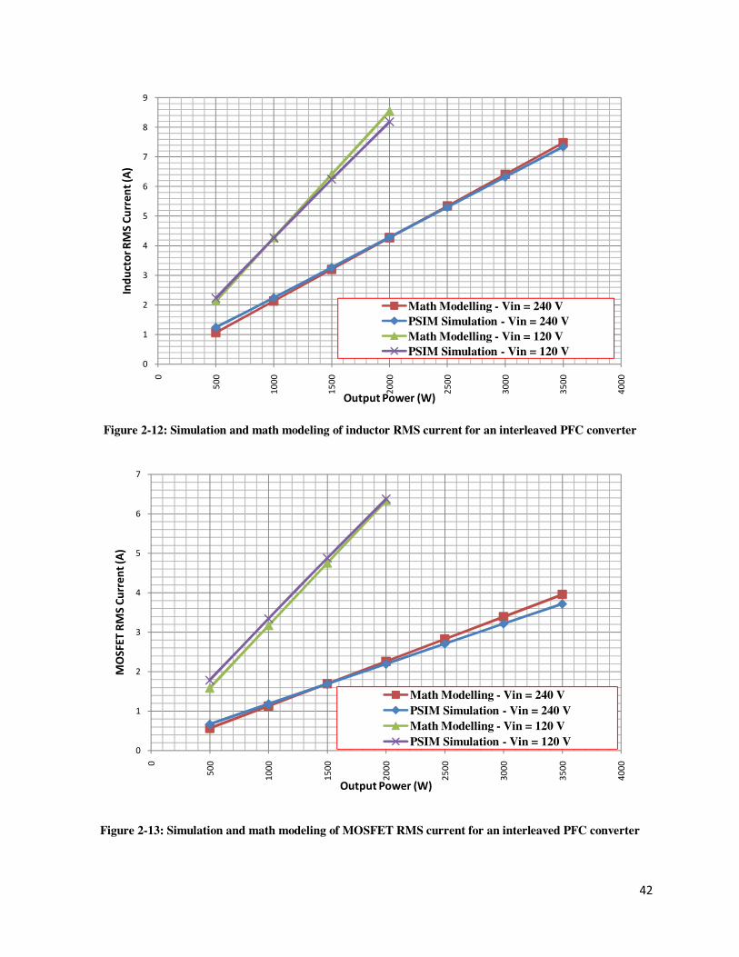
42
Figure 2-12: Simulation and math modeling of inductor RMS current for an interleaved PFC converter
Figure 2-13: Simulation and math modeling of MOSFET RMS current for an interleaved PFC converter
0
1
2
3
4
5
6
7
8
9
0
50
0
10
00
15
00
20
00
25
00
30
00
35
00
40
00
Ind
uct
or
RM
S C
urr
en
t (A
)
Output Power (W)
Math Modelling - Vin = 240 V
PSIM Simulation - Vin = 240 V
Math Modelling - Vin = 120 V
PSIM Simulation - Vin = 120 V
0
1
2
3
4
5
6
7
0
50
0
10
00
15
00
20
00
25
00
30
00
35
00
40
00
MO
SF
ET
RM
S C
urr
en
t (A
)
Output Power (W)
Math Modelling - Vin = 240 V
PSIM Simulation - Vin = 240 V
Math Modelling - Vin = 120 V
PSIM Simulation - Vin = 120 V
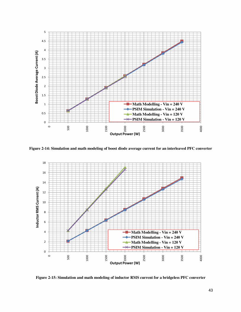
43
Figure 2-14: Simulation and math modeling of boost diode average current for an interleaved PFC converter
Figure 2-15: Simulation and math modeling of inductor RMS current for a bridgeless PFC converter
0
0.5
1
1.5
2
2.5
3
3.5
4
4.5
5
0
50
0
10
00
15
00
20
00
25
00
30
00
35
00
40
00
Bo
ost
Dio
de
Av
era
ge
Cu
rre
nt
(A)
Output Power (W)
Math Modelling - Vin = 240 V
PSIM Simulation - Vin = 240 V
Math Modelling - Vin = 120 V
PSIM Simulation - Vin = 120 V
0
2
4
6
8
10
12
14
16
18
0
50
0
10
00
15
00
20
00
25
00
30
00
35
00
40
00
Ind
uct
or
RM
S C
urr
en
t (A
)
Output Power (W)
Math Modelling - Vin = 240 V
PSIM Simulation - Vin = 240 V
Math Modelling - Vin = 120 V
PSIM Simulation - Vin = 120 V
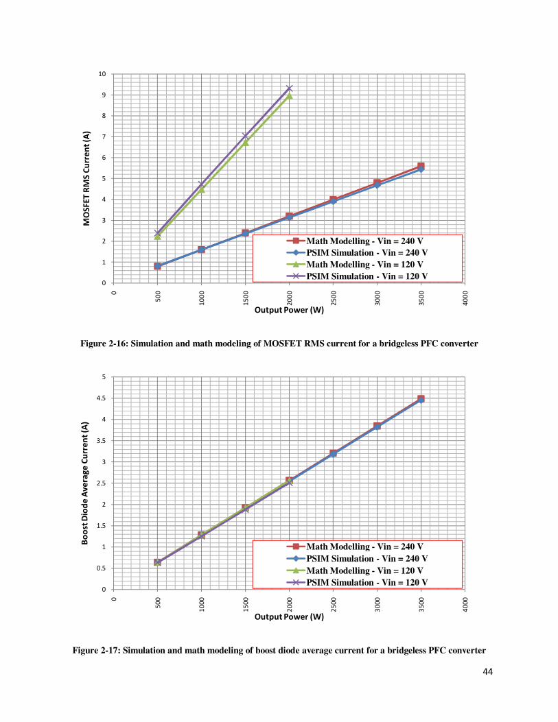
44
Figure 2-16: Simulation and math modeling of MOSFET RMS current for a bridgeless PFC converter
Figure 2-17: Simulation and math modeling of boost diode average current for a bridgeless PFC converter
0
1
2
3
4
5
6
7
8
9
10
0
50
0
10
00
15
00
20
00
25
00
30
00
35
00
40
00
MO
SF
ET
RM
S C
urr
en
t (A
)
Output Power (W)
Math Modelling - Vin = 240 V
PSIM Simulation - Vin = 240 V
Math Modelling - Vin = 120 V
PSIM Simulation - Vin = 120 V
0
0.5
1
1.5
2
2.5
3
3.5
4
4.5
5
0
50
0
10
00
15
00
20
00
25
00
30
00
35
00
40
00
Bo
ost
Dio
de
Av
era
ge
Cu
rre
nt
(A)
Output Power (W)
Math Modelling - Vin = 240 V
PSIM Simulation - Vin = 240 V
Math Modelling - Vin = 120 V
PSIM Simulation - Vin = 120 V

45
Figure 2-18: Simulation and math modeling of MOSFET body diode average current for a bridgeless PFC
2.5. Simulation Results
PSIM simulation software was used to verify steady state waveforms of each component.
Figure 2-19 shows the PSIM simulation circuits of the proposed BLIL PFC converter. As it can
be seen, the power stage section of converter consists of four boost inductors, Ld1 to Ld4, four
fast boost diodes, Db1 to Db4, four switches, Q1 to Q4 and their body diodes Dq1 to Dq4. Also
it consists of two current loops and one voltage loop. The sensed input voltage is multiplied by
the compensated output voltage, and then generates a control signal to be compared with the
switching carrier waveforms to generate the gating signals for the main MOSFETs.
0
1
2
3
4
5
6
7
8
9
0
50
0
10
00
15
00
20
00
25
00
30
00
35
00
40
00
MO
SF
ET
Bo
dy
Dio
de
Av
era
ge
Cu
rre
nt
(A)
Output Power (W)
Math Modelling - Vin = 240 V
PSIM Simulation - Vin = 240 V
Math Modelling - Vin = 120 V
PSIM Simulation - Vin = 120 V
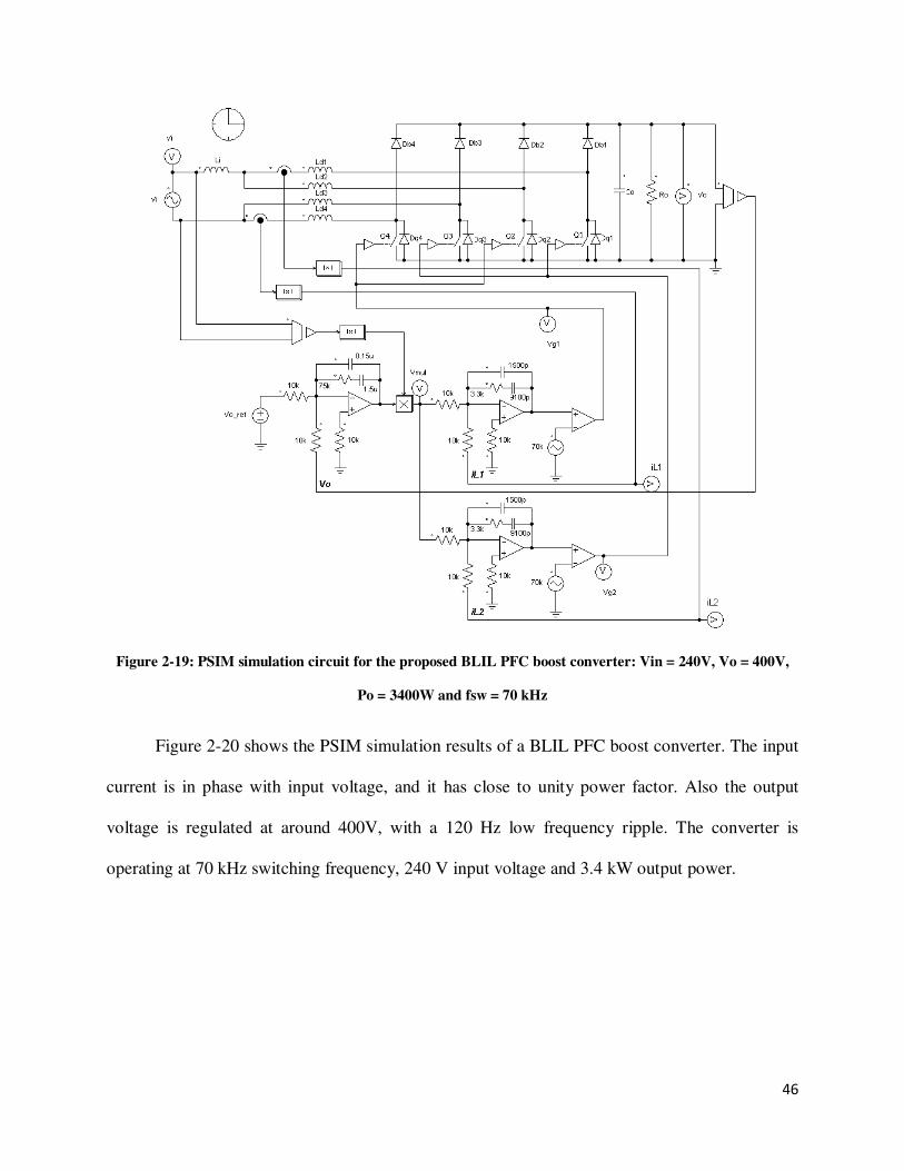
46
Figure 2-19: PSIM simulation circuit for the proposed BLIL PFC boost converter: Vin = 240V, Vo = 400V,
Po = 3400W and fsw = 70 kHz
Figure 2-20 shows the PSIM simulation results of a BLIL PFC boost converter. The input
current is in phase with input voltage, and it has close to unity power factor. Also the output
voltage is regulated at around 400V, with a 120 Hz low frequency ripple. The converter is
operating at 70 kHz switching frequency, 240 V input voltage and 3.4 kW output power.
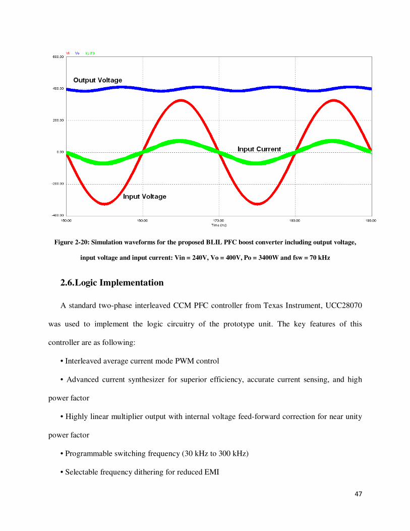
47
Figure 2-20: Simulation waveforms for the proposed BLIL PFC boost converter including output voltage,
input voltage and input current: Vin = 240V, Vo = 400V, Po = 3400W and fsw = 70 kHz
2.6. Logic Implementation
A standard two-phase interleaved CCM PFC controller from Texas Instrument, UCC28070
was used to implement the logic circuitry of the prototype unit. The key features of this
controller are as following:
• Interleaved average current mode PWM control
• Advanced current synthesizer for superior efficiency, accurate current sensing, and high
power factor
• Highly linear multiplier output with internal voltage feed-forward correction for near unity
power factor
• Programmable switching frequency (30 kHz to 300 kHz)
• Selectable frequency dithering for reduced EMI
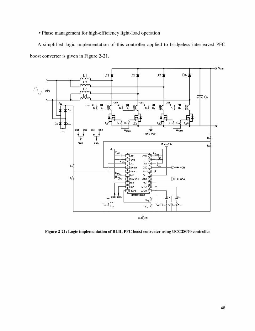
48
• Phase management for high-efficiency light-load operation
A simplified logic implementation of this controller applied to bridgeless interleaved PFC
boost converter is given in Figure 2-21.
Figure 2-21: Logic implementation of BLIL PFC boost converter using UCC28070 controller

49
2.7. Experimental Results
An experimental prototype, illustrated in Figure 2-22, was built to verify the operation of the
proposed converter. Figure 2-23 shows the input voltage, input current and PFC bus voltage of
the converter under the following test conditions: Vin = 240 V, Iin = 15 A, Po = 3400 W, Vo =
400 V, fsw = 70 kHz. The input current is in line and phase with the input voltage, and its shape
is close to a sinusoidal waveform. Table 2-3 shows the semiconductors and power components
used in the 3.4 kW CCM experimental prototype, a bridgeless interleaved PFC converter.
Figure 2-22: Breadboard prototype of BLIL PFC boost converter

50
Figure 2-23: Breadboard proposed BLIL PFC experimental waveforms;
Test condition: Po = 3400W, Vin = 240V, Iin = 15A.
Figure 2-24: Gating signal, boost MOSFET and diode current for D > 0.5
Input Voltage
Ch2 = Vin 100V/div.
Output Voltage Ch1= Vo 100V/div.
Input Current
Ch3 = Iin 10A/div.
Diode Current
Ch3 = ID1 2A/div.
Gating Signal
Ch1 = Vg 10V/div.
MOSFET Current
Ch4 = IQ1 2A/div.
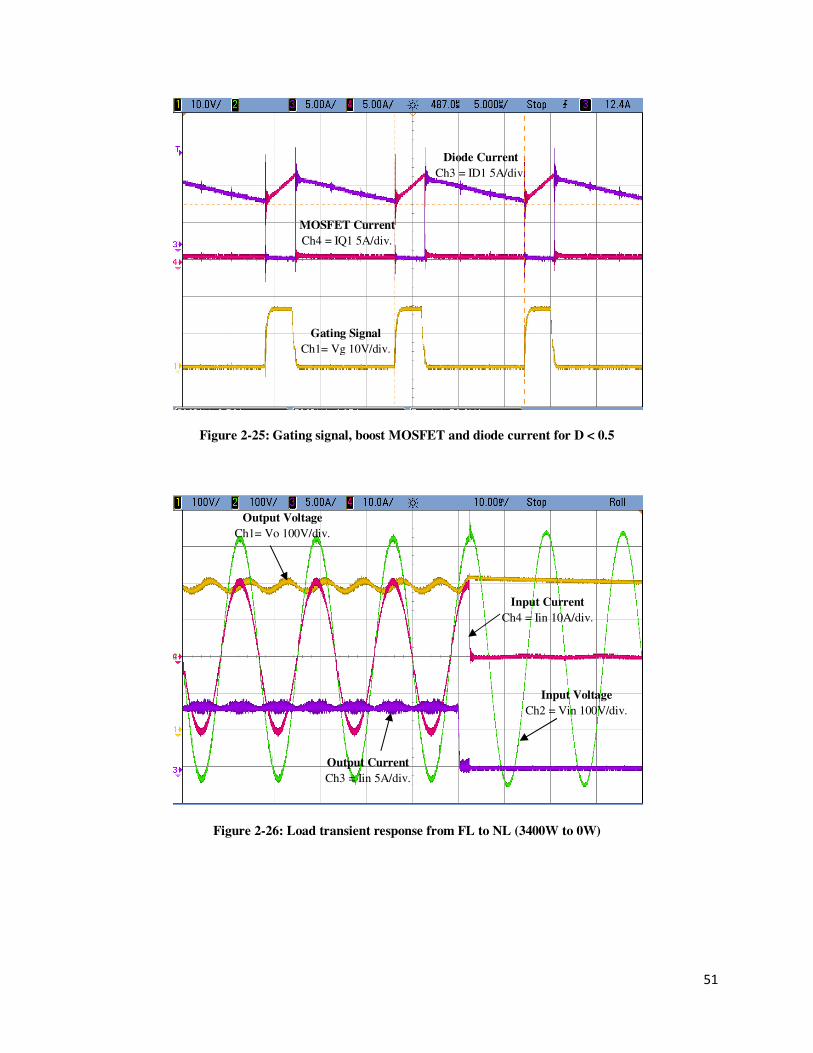
51
Figure 2-25: Gating signal, boost MOSFET and diode current for D < 0.5
Figure 2-26: Load transient response from FL to NL (3400W to 0W)
Diode Current
Ch3 = ID1 5A/div.
Gating Signal
Ch1= Vg 10V/div.
MOSFET Current
Ch4 = IQ1 5A/div.
Input Voltage
Ch2 = Vin 100V/div.
Output Voltage Ch1= Vo 100V/div.
Input Current
Ch4 = Iin 10A/div.
Output Current
Ch3 = Iin 5A/div.
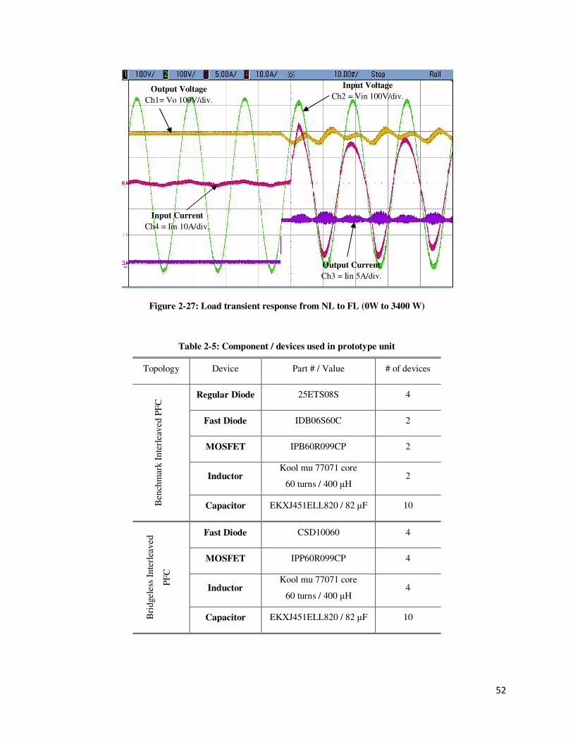
52
Figure 2-27: Load transient response from NL to FL (0W to 3400 W)
Table 2-5: Component / devices used in prototype unit
Topology Device Part # / Value # of devices
Ben
chm
ark I
nte
rlea
ved
PF
C Regular Diode 25ETS08S 4
Fast Diode IDB06S60C 2
MOSFET IPB60R099CP 2
Inductor Kool mu 77071 core
60 turns / 400 µH 2
Capacitor EKXJ451ELL820 / 82 µF 10
Bri
dgel
ess
Inte
rlea
ved
PF
C
Fast Diode CSD10060 4
MOSFET IPP60R099CP 4
Inductor Kool mu 77071 core
60 turns / 400 µH 4
Capacitor EKXJ451ELL820 / 82 µF 10
Input Voltage
Ch2 = Vin 100V/div. Output Voltage
Ch1= Vo 100V/div.
Input Current
Ch4 = Iin 10A/div.
Output Current
Ch3 = Iin 5A/div.
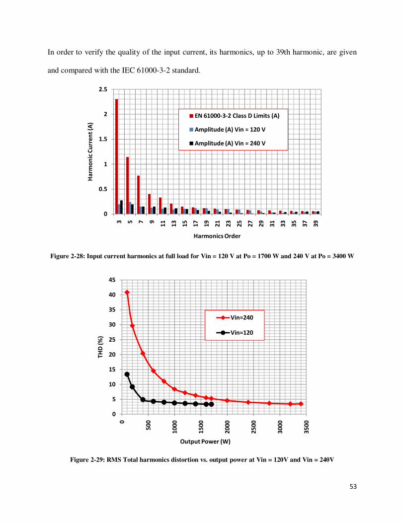
53
In order to verify the quality of the input current, its harmonics, up to 39th harmonic, are given
and compared with the IEC 61000-3-2 standard.
Figure 2-28: Input current harmonics at full load for Vin = 120 V at Po = 1700 W and 240 V at Po = 3400 W
Figure 2-29: RMS Total harmonics distortion vs. output power at Vin = 120V and Vin = 240V
0
0.5
1
1.5
2
2.5
3 5 7 9
11
13
15
17
19
21
23
25
27
29
31
33
35
37
39
Ha
rmo
nic
Cu
rre
nt
(A)
Harmonics Order
EN 61000-3-2 Class D Limits (A)
Amplitude (A) Vin = 120 V
Amplitude (A) Vin = 240 V
0
5
10
15
20
25
30
35
40
45
0
50
0
10
00
15
00
20
00
25
00
30
00
35
00
TH
D (
%)
Output Power (W)
Vin=240
Vin=120
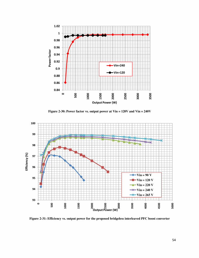
54
Figure 2-30: Power factor vs. output power at Vin = 120V and Vin = 240V
Figure 2-31: Efficiency vs. output power for the proposed bridgeless interleaved PFC boost converter
0.84
0.86
0.88
0.9
0.92
0.94
0.96
0.98
1
1.02
0
50
0
10
00
15
00
20
00
25
00
30
00
35
00
Po
we
r fa
cto
r
Output Power (W)
Vin=240
Vin=120
93
94
95
96
97
98
99
100
0
50
0
10
00
15
00
20
00
25
00
30
00
35
00
40
00
45
00
50
00
Eff
icie
ncy
(%
)
Output Power (W)
Vin = 90 V
Vin = 120 V
Vin = 220 V
Vin = 240 V
Vin = 265 V
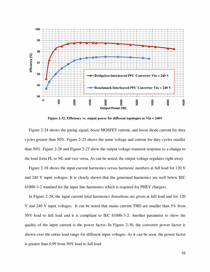
55
Figure 2-32: Efficiency vs. output power for different topologies at Vin = 240V
Figure 2-24 shows the gating signal, boost MOSFET current, and boost diode current for duty
cycles greater than 50%. Figure 2-25 shows the same voltage and current for duty cycles smaller
than 50%. Figure 2-26 and Figure 2-27 show the output voltage transient response to a change to
the load form FL to NL and vice versa. As can be noted, the output voltage regulates right away.
Figure 2-28 shows the input current harmonics versus harmonic numbers at full load for 120 V
and 240 V input voltages. It is clearly shown that the generated harmonics are well below IEC
61000-3-2 standard for the input line harmonics which is required for PHEV chargers.
In Figure 2-29, the input current total harmonics distortions are given at full load and for 120
V and 240 V input voltages. It can be noted that mains current THD are smaller than 5% from
50% load to full load and it is compliant to IEC 61000-3-2. Another parameter to show the
quality of the input current is the power factor. In Figure 2-30, the converter power factor is
shown over the entire load range for different input voltages. As it can be seen, the power factor
is greater than 0.99 from 50% load to full load.
94
95
96
97
98
99
100
0
50
0
10
00
15
00
20
00
25
00
30
00
35
00
40
00
45
00
Eff
icie
ncy
(%
)
Output Power (W)
Bridgeless Interleaved PFC Converter Vin = 240 V
Benchmark Interleaved PFC Converter Vin = 240 V

56
The efficiency of converter versus output power for different input voltages is provided in
Figure 2-31. With the proposed bridgeless interleaved PFC converter a peak efficiency of
98.94% was reached at 265 V input and 1.2 kW output power. High efficiency over the entire
load range is achieved in this topology, enabling fewer problems with heat dissipation and
cooling systems. Furthermore, a higher efficiency means more power is available from the mains
feed to charge the batteries, reducing charging time and electricity costs.
Figure 2-32 illustrates the measured experimental efficiency of benchmark interleaved
boost PFC and BLIL boost PFC topology discussed in this chapter for 240 V input voltage. The
proposed BLIL PFC converter has the highest efficiency over the entire load range.
Figure 2-33: Loss reduction as a function of output power at Vin = 240V, Vo = 400 V and 70 kHz for the
proposed BLIL converter compared to the benchmark interleaved boost converter
0
10
20
30
40
50
60
70
0
50
0
10
00
15
00
20
00
25
00
30
00
35
00
Loss
Re
du
ctio
n (
%)
Output Power (W)

57
Loss reduction curves as a function of output power for BLIL PFC against benchmark IL
PFC are provided in Figure 2-33 and Figure 2-34 for 240 V and 120 V.
Figure 2-34: Loss reduction as a function of output power at Vin = 120V, Vo = 400 V and 70 kHz for the
proposed BLIL converter compared to the benchmark interleaved boost converter
2.8. Conclusion
A high performance AC-DC boost converter topology has been presented in this chapter for
the front-end AC-DC converter in PHEV battery chargers. The proposed converter topology has
been analyzed and performance characteristics presented. Also an analytical model for the four
different topologies was developed, enabling the calculation of power losses and efficiencies. A
prototype converter was built to verify this proof-of-concept. The theoretical waveforms were
compared with the results taken from prototype unit. Also some key experimental waveforms
0
10
20
30
40
50
60
0
20
0
40
0
60
0
80
0
10
00
12
00
14
00
16
00
18
00
Loss
Re
du
ctio
n (
%)
Output Power (W)

58
were given. Finally, input current harmonics at each harmonic order were compared more
explicitly with the IEC 61000-3-2 standard limits. It can be noted that mains current THD are
smaller than 5% from 50% load to full load and the converter is compliant with the IEC 6100-3-
2 standard. The converter power factor was also provided for full power range and different input
voltages. It can be seen that the power factor is greater than 0.99 from 50% load to full load. The
proposed converter achieves a peak efficiency of 98.94 % at 265 V input and 1.2 kW output
power.
The converter topology shows a high input power factor, high efficiency over the entire
load range, and excellent input current harmonics. It is a potential option for single phase PFC in
higher power battery charging applications.

59
CHAPTER 3. Phase-Shifted Semi Bridgeless PFC Converter
3.1. Introduction
In this chapter, a phase shifted semi-bridgeless boost power factor corrected converter is
proposed for plug in hybrid electric vehicle battery chargers. The converter features high
efficiency at light loads and low lines, which is critical to minimize the charger size, charging
time, and the amount and cost of electricity drawn from the utility; the component count, which
reduces the charger cost; and reduced EMI. The converter is ideally suited for automotive level 1
residential charging applications.
A detailed converter description and steady state operation analysis of this converter is
presented. Experimental results of a prototype boost converter, converting universal AC input
voltage to 400 V DC at 3.4 kW are given and the results are compared to a benchmark
interleaved boost converter to verify the proof of concept, and analytical work reported. The
results show a power factor greater than 0.99 from 750 W to 3.4 kW, THD less than 5% from
half load to full load, a peak efficiency of 98.6 % at 240 V input, and 1000 W load.
3.2. Circuit Description and Steady State Analysis
The phase shifted semi-bridgeless topology [84], shown in Figure 3-1, is proposed as another
solution to address the problems outlined in chapter 1 for the conventional boost, bridgeless
boost and interleaved boost topologies. The proposed topology has high efficiency at light loads
and low lines, which is important to minimize the charger size, charging time, and the amount
and cost of electricity drawn from the utility; the component count, which reduces the charger
cost; and reduced EMI. The converter is ideally suited for automotive level 1 residential charging
applications in North America where the typical supply is limited to 120V and 1.44kVA.

60
Figure 3-1: Phase shifted semi-bridgeless PFC boost topology
The proposed topology introduces two more slow diodes (Da and Db) to the bridgeless
configuration to link the ground of the PFC to the input line. However, the current does not
always return through these diodes, so their associated conduction losses are low. This occurs
since the inductors exhibit low impedance at the line frequency, a large portion of the current
flows through the MOSFET intrinsic body diodes. Also the gating signals for MOSFETs are
180° out of phase. To analyze the circuit operation, the input line cycle has been separated into
the positive and negative half-cycles, as explained in the sub-sections that follow. In addition, the
detailed circuit operation depends on the duty cycle. Positive half-cycle operation analysis is
provided for D > 0.5 and D < 0.5.
3.2.1. Positive Half Cycle Operation
Referring to Figure 3-1, during the positive half-cycle, when the AC input voltage is
positive, Q1 turns on and current flows through L1 and Q1 and continues through Q2 and then
L2, returning to the line while storing energy in L1 and L2. When Q1 turns off, energy stored in
L1 and L2 is released as current flows through D1, through the load and returns through the body
diode of Q2/partially through Db back to the input.

61
3.2.2. Negative Half Cycle Operation
Referring to Figure 3-1, during the negative half-cycle, when the AC input voltage is
negative, Q2 turns on and current flows through L2 and Q2 and continues through Q1 and then
L1, returning to the line while storing energy in L2 and L1. When Q2 turns off, energy stored in
L2 and L1 is released as current flows through D2, through the load and returns split between the
body diode of Q1 and Da back to the input.
3.2.1. Detailed Positive Half Cycle Operation and Analysis for D > 0.5
The detailed operation of the proposed converter depends on the duty cycle. During any
half-cycle, the converter duty cycle is either greater than 0.5 (when the input voltage is smaller
than half of output voltage) or smaller than 0.5 (when the input voltage is greater than half of
output voltage). The three unique operating interval circuits of the proposed converter are
provided in Figure 3-2 to Figure 3-4 for duty cycles larger than 0.5 during the positive half-cycle.
Waveforms of the proposed converter during positive half-cycle operation with D>0.5 are
shown in Figure 3-5. The intervals of operation are explained as follows. In addition, the ripple
current components are derived, enabling calculation of the input ripple current, which provides
design guidance to meet the required input current ripple standard.
D1 D2
Q1 Q2
CO
L1
L2
L
O
A
D
Vin
Vg1 Vg2
DaDb
Figure 3-2: Interval 1and 3: Q1 and Q2 are ON
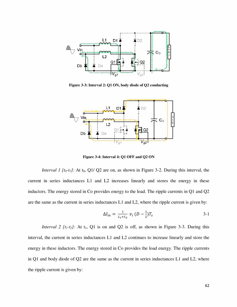
62
Figure 3-3: Interval 2: Q1 ON, body diode of Q2 conducting
Figure 3-4: Interval 4: Q1 OFF and Q2 ON
Interval 1 [t0-t1]: At t0, Q1/ Q2 are on, as shown in Figure 3-2. During this interval, the
current in series inductances L1 and L2 increases linearly and stores the energy in these
inductors. The energy stored in Co provides energy to the load. The ripple currents in Q1 and Q2
are the same as the current in series inductances L1 and L2, where the ripple current is given by:
∆G6 &A -A+ 56 ) − &H': 3-1
Interval 2 [t1-t2]: At t1, Q1 is on and Q2 is off, as shown in Figure 3-3. During this
interval, the current in series inductances L1 and L2 continues to increase linearly and store the
energy in these inductors. The energy stored in Co provides the load energy. The ripple currents
in Q1 and body diode of Q2 are the same as the current in series inductances L1 and L2, where
the ripple current is given by:

63
∆G6 &A -A+ 56 1 − )': 3-2
Interval 3 [t2-t3]: At t2, Q1/Q2 are on again, and interval 1 is repeated, as shown in Figure
3-2. During this interval, the current in series inductances L1 and L2 increases linearly and stores
the energy in these inductors. The ripple currents in Q1 and Q2 are the same as the ripple current
in series inductances L1 and L2, as shown in equation (3-1).
Interval 4 [t3-t4]: At t3, Q1 is off and Q2 is on, as shown in Figure 3-4. During this
interval, the energy stored in L1 and L2 is released to the output through L1, D1, Q2 and L2. The
ripple currents in D1 and Q2 are the same as the ripple currents in L1 and L2:
∆G6 &A -A+ 56 − 91 − )': 3-3
Figure 3-5: Phase shifted semi-bridgeless boost converter steady-state waveforms at D > 0.5
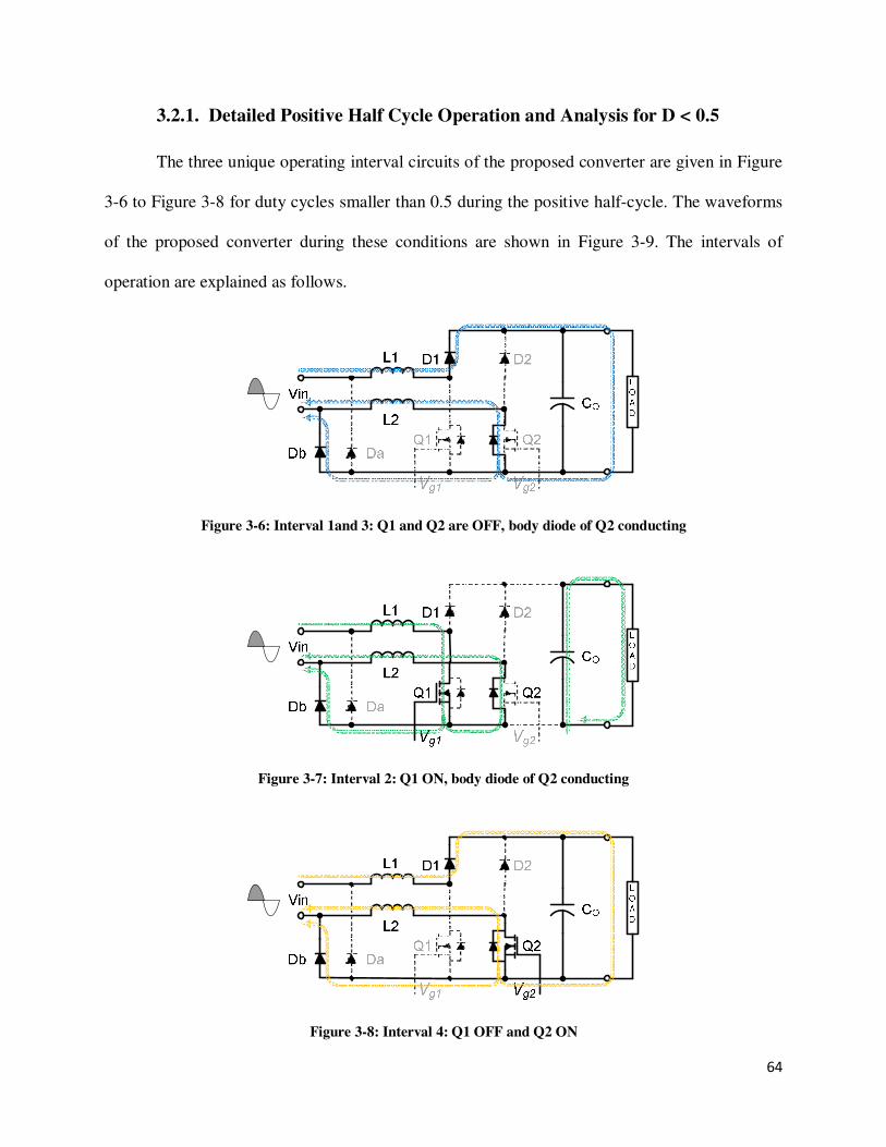
64
3.2.1. Detailed Positive Half Cycle Operation and Analysis for D < 0.5
The three unique operating interval circuits of the proposed converter are given in Figure
3-6 to Figure 3-8 for duty cycles smaller than 0.5 during the positive half-cycle. The waveforms
of the proposed converter during these conditions are shown in Figure 3-9. The intervals of
operation are explained as follows.
Figure 3-6: Interval 1and 3: Q1 and Q2 are OFF, body diode of Q2 conducting
Figure 3-7: Interval 2: Q1 ON, body diode of Q2 conducting
Figure 3-8: Interval 4: Q1 OFF and Q2 ON
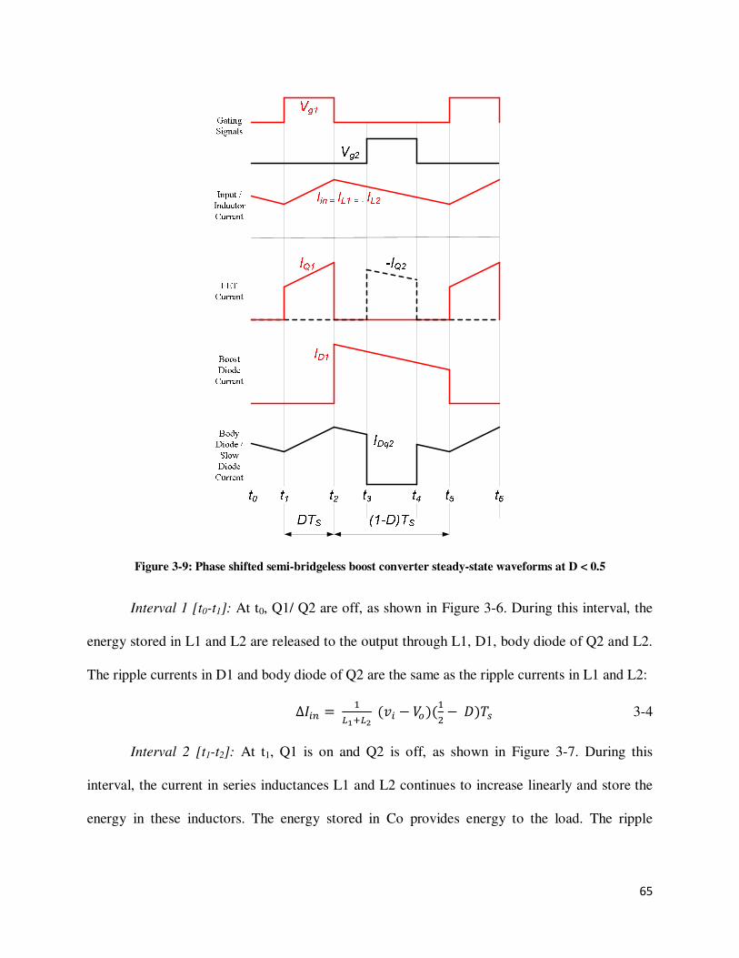
65
Figure 3-9: Phase shifted semi-bridgeless boost converter steady-state waveforms at D < 0.5
Interval 1 [t0-t1]: At t0, Q1/ Q2 are off, as shown in Figure 3-6. During this interval, the
energy stored in L1 and L2 are released to the output through L1, D1, body diode of Q2 and L2.
The ripple currents in D1 and body diode of Q2 are the same as the ripple currents in L1 and L2:
∆G6 &A -A+ 56 − 9&H − )': 3-4 Interval 2 [t1-t2]: At t1, Q1 is on and Q2 is off, as shown in Figure 3-7. During this
interval, the current in series inductances L1 and L2 continues to increase linearly and store the
energy in these inductors. The energy stored in Co provides energy to the load. The ripple

66
currents in Q1 and the body diode of Q2 are the same as the current in series inductances L1 and
L2, where the ripple current is given by:
∆G6 &A -A+ 56 )': 3-5 Interval 3 [t2-t3]: At t2, Q1/Q2 are off again, and interval 1 is repeated, as shown in
Figure 3-6. During this interval, the current in series inductances L1 and L2 increases linearly
and stores the energy in these inductors. The ripple currents in D1 and body diode of Q2 are the
same as the ripple current in series inductances L1 and L2, as shown in equation (3-4).
Interval 4 [t3-t4]: At t3, Q1 is off and Q2 is on, as shown in Figure 3-8. During this
interval, the energy stored in L1 and L2 is released to the output through L1, D1, Q2 and L2. The
ripple currents in D1 and Q2 are the same as the ripple currents in L1 and L2:
∆G6 &A -A+ 56 − 9)': 3-6 The operation of converter during the negative input voltage half-cycle is similar to the operation
of converter during the positive input voltage half-cycle.
3.3. Loss Modeling
The estimated loss distribution of the semiconductors is provided in Figure 3-10 at 70 kHz
switching frequency, 240V input and 3300W load for benchmark conventional boost and
benchmark interleaved boost converters and the proposed phase shifted semi-bridgeless boost
converter. The currents in regular diodes Da and Db were assumed to be split with the current
going through intrinsic body diodes for phase shifted semi-bridgeless topology. The regular
diodes input bridge rectifiers have the largest share of losses among the topologies with the input
bridge rectifier. The phase shifted semi-bridgeless topology nearly eliminates this large loss
component (~27.6W). However, the tradeoff is that the MOSFET losses are higher and the
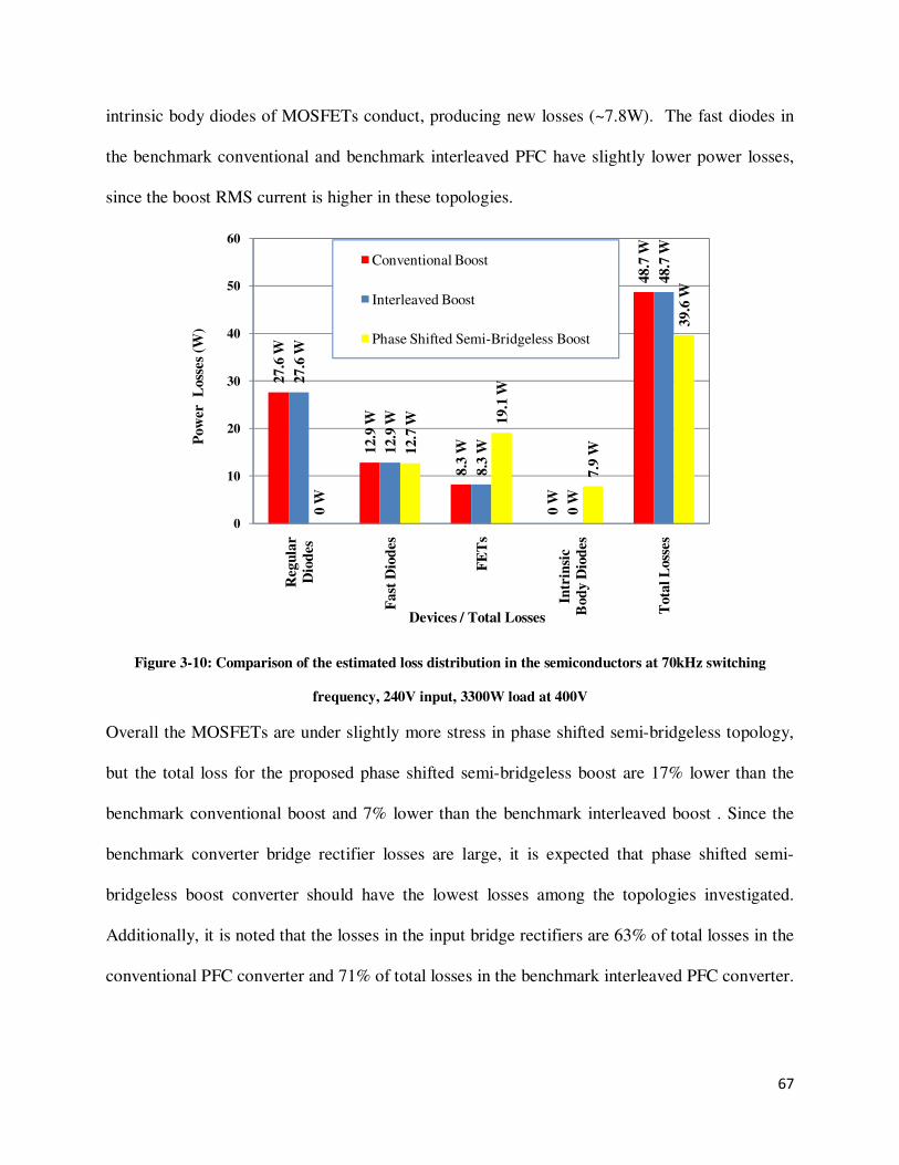
67
intrinsic body diodes of MOSFETs conduct, producing new losses (~7.8W). The fast diodes in
the benchmark conventional and benchmark interleaved PFC have slightly lower power losses,
since the boost RMS current is higher in these topologies.
Figure 3-10: Comparison of the estimated loss distribution in the semiconductors at 70kHz switching
frequency, 240V input, 3300W load at 400V
Overall the MOSFETs are under slightly more stress in phase shifted semi-bridgeless topology,
but the total loss for the proposed phase shifted semi-bridgeless boost are 17% lower than the
benchmark conventional boost and 7% lower than the benchmark interleaved boost . Since the
benchmark converter bridge rectifier losses are large, it is expected that phase shifted semi-
bridgeless boost converter should have the lowest losses among the topologies investigated.
Additionally, it is noted that the losses in the input bridge rectifiers are 63% of total losses in the
conventional PFC converter and 71% of total losses in the benchmark interleaved PFC converter.
27.6
W
12
.9 W
8.3
W
0 W
48.7
W
27.6
W
12
.9 W
8.3
W
0 W
48.7
W
0 W
12
.7 W 1
9.1
W
7.9
W
39.6
W
0
10
20
30
40
50
60
Reg
ula
r
Dio
des
Fa
st D
iod
es
FE
Ts
Intr
insi
c
Bod
y D
iod
es
Tota
l L
oss
es
Pow
er
Loss
es
(W)
Devices / Total Losses
Conventional Boost
Interleaved Boost
Phase Shifted Semi-Bridgeless Boost
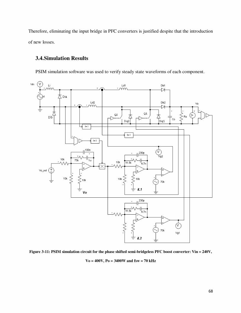
68
Therefore, eliminating the input bridge in PFC converters is justified despite that the introduction
of new losses.
3.4. Simulation Results
PSIM simulation software was used to verify steady state waveforms of each component.
Figure 3-11: PSIM simulation circuit for the phase shifted semi-bridgeless PFC boost converter: Vin = 240V,
Vo = 400V, Po = 3400W and fsw = 70 kHz

69
Figure 3-11 shows the PSIM simulation circuits of the proposed BLIL PFC converter. As it can
be seen, the power stage section of converter consists of two boost inductors, Ld1 and Ld2, two
fast boost diodes, Db1 and Db2, two switches, Q1 and Q2 and their body diodes Dq1 and Dq2.
Also it consists of two current loops and one voltage loop. The sensed input voltage is multiplied
by the compensated output voltage, and then generates a control signal to be compared with the
switching carrier waveforms to generate the gating signals for main MOSFETs.
Figure 3-12 shows the PSIM simulation results of a phase shifted semi-bridgeless PFC
boost converter. The input current is in phase with the input voltage, and it has close to unity
power factor. Also the output voltage is regulated at around 400V, with a 120 Hz low frequency
ripple. The converter is operating at 70 kHz switching frequency, 240 V input voltage and 3.4
kW output power.
Figure 3-12: Simulation waveforms for the proposed phase shifted semi-bridgeless PFC boost converter:
Output voltage, input voltage and input current: Vin = 240V, Vo = 400V, Po = 3400W and fsw = 70 kHz
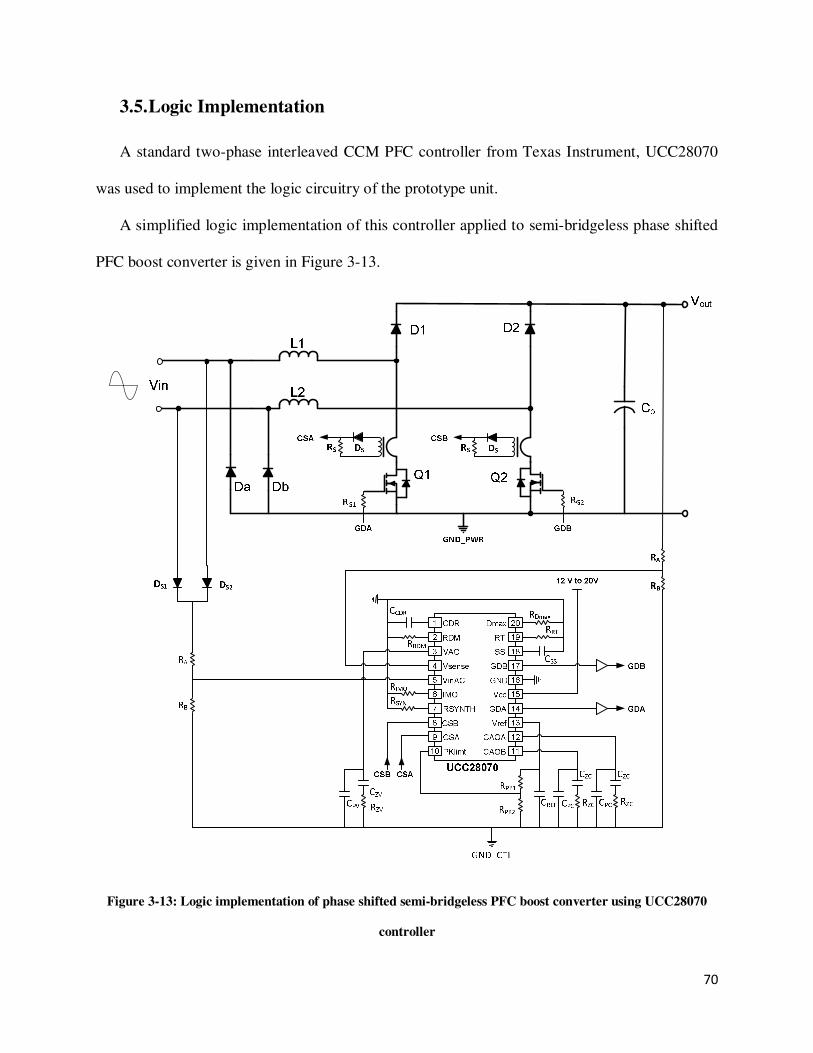
70
3.5. Logic Implementation
A standard two-phase interleaved CCM PFC controller from Texas Instrument, UCC28070
was used to implement the logic circuitry of the prototype unit.
A simplified logic implementation of this controller applied to semi-bridgeless phase shifted
PFC boost converter is given in Figure 3-13.
Figure 3-13: Logic implementation of phase shifted semi-bridgeless PFC boost converter using UCC28070
controller

71
3.6. Experimental Results
Prototypes of a phase shifted bridgeless boost converter and a benchmark interleaved
boost converter were built to verify the proof-of-concept and analytical work presented in this
chapter and to benchmark the proposed converter. The devices used in experimental prototypes
are provided in Table 3-1.
Table 3-1: Component / devices used in prototype unit
Topology Components Used in Prototype Unit Head
Device Part # / Value # of Devices
Ph
ase
Shif
ted S
emi-
bri
dgel
ess
PF
C Regular Diode 25ETS08S 2
Fast Diode IDB06S60C 2
MOSFET IPB60R099CP 2
Inductors
Kool mu 77071 core
60 turns / 400 µH
2
Capacitors EKXJ451ELL820 / 82 µF 10
Ben
chm
ark I
nte
rlea
ved
PF
C
Regular Diode 25ETS08S 4
Fast Diode IDB06S60C 2
MOSFET IPB60R099CP 2
Inductors
Kool mu 77071 core
60 turns / 400 µH
2
Capacitors EKXJ451ELL820 / 82 µF 10
Pictures of the proposed phase shifted bridgeless boost prototype are provided in Figure 3-14
to Figure 3-16. It consists of a capacitor bank of 820 µF, a control board and an IMS power
board attached to a heatsink with the PFC inductors.
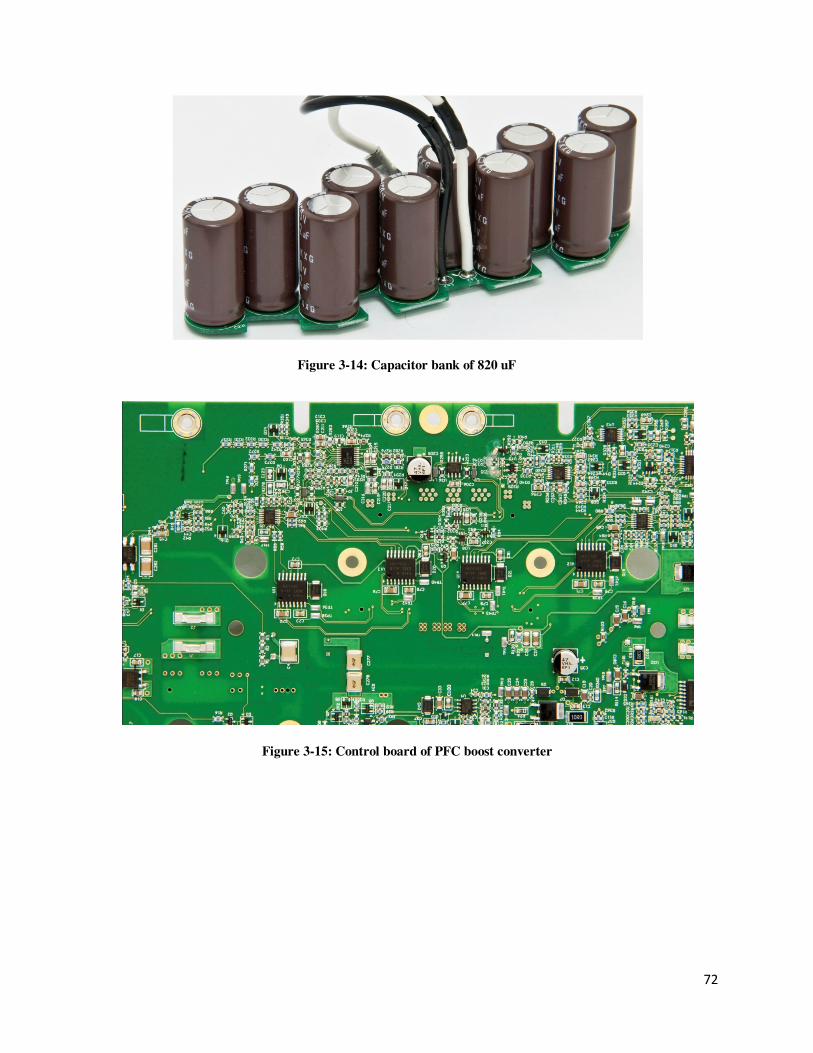
72
Figure 3-14: Capacitor bank of 820 uF
Figure 3-15: Control board of PFC boost converter
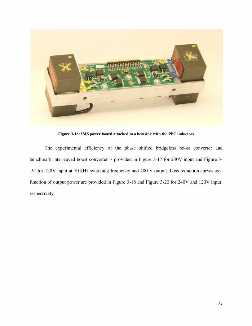
73
Figure 3-16: IMS power board attached to a heatsink with the PFC inductors
The experimental efficiency of the phase shifted bridgeless boost converter and
benchmark interleaved boost converter is provided in Figure 3-17 for 240V input and Figure 3-
19 for 120V input at 70 kHz switching frequency and 400 V output. Loss reduction curves as a
function of output power are provided in Figure 3-18 and Figure 3-20 for 240V and 120V input,
respectively.

74
Figure 3-17: Efficiency as a function of output power at Vin = 240V, Vo=400V and 70kHz switching
Figure 3-18: Loss reduction as a function of output power at Vin = 240V, Vo=400V and 70kHz for the
proposed phase shifted semi-bridgeless converter compared to the benchmark interleaved boost converter
94
95
96
97
98
99
100
0
50
0
10
00
15
00
20
00
25
00
30
00
35
00
Eff
icie
ncy
(%
)
Output Power (W)
Interleaved PFC Converter
Phase Shifted Semi-Bridgeless
PFC Converter
0
10
20
30
40
50
60
70
0
50
0
10
00
15
00
20
00
25
00
30
00
35
00
Loss
Re
du
ctio
n (
%)
Output Power (W)

75
Figure 3-19: Efficiency as a function of output power at Vin = 120V, Vo=400V and 70kHz
Figure 3-20: Loss reduction as a function of output power at Vin = 120V, Vo=400V and 70kHz for the
proposed phase shifted semi-bridgeless converter compared to the benchmark interleaved boost converter
From the results, it is noted that proposed semi-bridgeless PFC converter achieves a peak
efficiency of 98.6% at 1 kW output power. Additionally, the light load efficiency of the
91
92
93
94
95
96
97
98
0
20
0
40
0
60
0
80
0
10
00
12
00
14
00
16
00
18
00
Eff
icie
ncy
(%
)
Output Power (W)
Interleaved PFC Converter
Phase Shifted Semi-Bridgeless
PFC Converter
0
10
20
30
40
50
60
70
0
20
0
40
0
60
0
80
0
10
00
12
00
14
00
16
00
18
00
Loss
Re
du
ctio
n (
%)
Output Power (W)
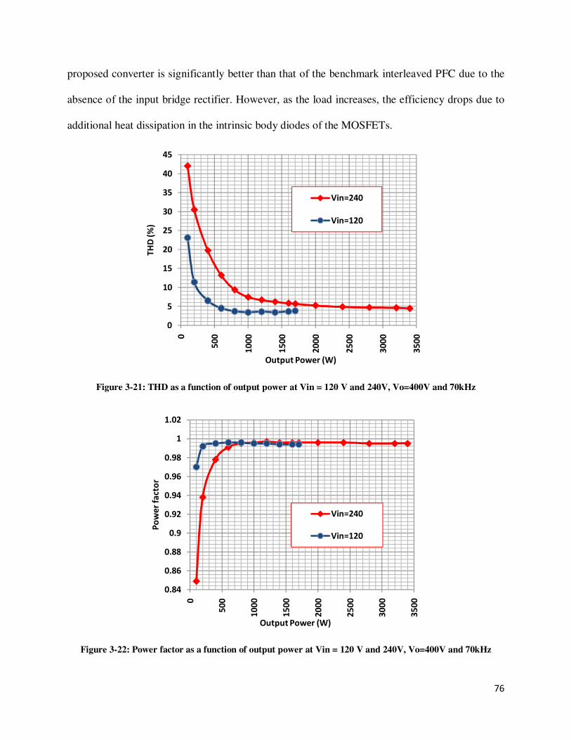
76
proposed converter is significantly better than that of the benchmark interleaved PFC due to the
absence of the input bridge rectifier. However, as the load increases, the efficiency drops due to
additional heat dissipation in the intrinsic body diodes of the MOSFETs.
Figure 3-21: THD as a function of output power at Vin = 120 V and 240V, Vo=400V and 70kHz
Figure 3-22: Power factor as a function of output power at Vin = 120 V and 240V, Vo=400V and 70kHz
0
5
10
15
20
25
30
35
40
45
0
50
0
10
00
15
00
20
00
25
00
30
00
35
00
TH
D (
%)
Output Power (W)
Vin=240
Vin=120
0.84
0.86
0.88
0.9
0.92
0.94
0.96
0.98
1
1.02
0
50
0
10
00
15
00
20
00
25
00
30
00
35
00
Po
we
r fa
cto
r
Output Power (W)
Vin=240
Vin=120

77
Figure 3-23: Harmonics orders at Vin = 120 V and 240V, compared against EN61000-3-2 standard for Vin =
120 V at Po = 1700 W and 240 V at Po = 3400 W
In order to verify the quality of the input current, the input current THD is shown in Figure 3-21.
The power factor and harmonic orders are given and compared with EN 61000-3-2 standard in
Figure 3-22 and Figure 3-23. It is noted that mains current THD is less than 5% from 50% load
to full load and it is compliant to IEC 61000-3-2 (Figure 3-21 and Figure 3-23). The converter
power factor is shown over entire load range for 120 and 240V input in Figure 3-22. The power
factor is greater than 0.99 from 50% load to full load.
Experimental waveforms from the proposed converter prototype are provided in Figure 3-24
through Figure 3-30. The input current, input voltage and output voltage are given in Figure 3-
24. As it can be seen, the input current is in phase with the input voltage and has a sinusoidal
shape. Additionally, there is a low frequency ripple on output voltage, which is inversely
proportional to the value of PFC bus output capacitors.
0
0.5
1
1.5
2
2.5
3 5 7 9
11
13
15
17
19
21
23
25
27
29
31
33
35
37
39
Am
pli
tud
e (
A)
Harmonics Order
EN 61000-3-2 Class D Limits (A)
Amplitude (A) Vin = 120 V
Amplitude (A) Vin = 240 V
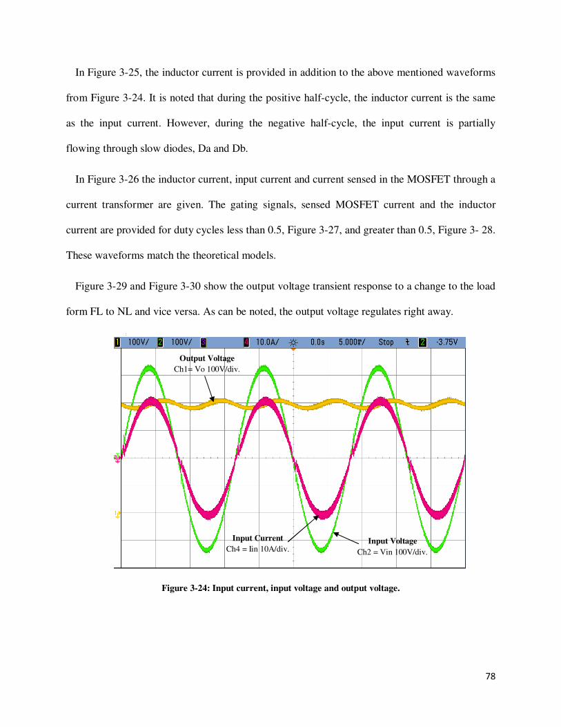
78
In Figure 3-25, the inductor current is provided in addition to the above mentioned waveforms
from Figure 3-24. It is noted that during the positive half-cycle, the inductor current is the same
as the input current. However, during the negative half-cycle, the input current is partially
flowing through slow diodes, Da and Db.
In Figure 3-26 the inductor current, input current and current sensed in the MOSFET through a
current transformer are given. The gating signals, sensed MOSFET current and the inductor
current are provided for duty cycles less than 0.5, Figure 3-27, and greater than 0.5, Figure 3- 28.
These waveforms match the theoretical models.
Figure 3-29 and Figure 3-30 show the output voltage transient response to a change to the load
form FL to NL and vice versa. As can be noted, the output voltage regulates right away.
Figure 3-24: Input current, input voltage and output voltage.
Input Voltage
Ch2 = Vin 100V/div.
Output Voltage Ch1= Vo 100V/div.
Input Current
Ch4 = Iin 10A/div.
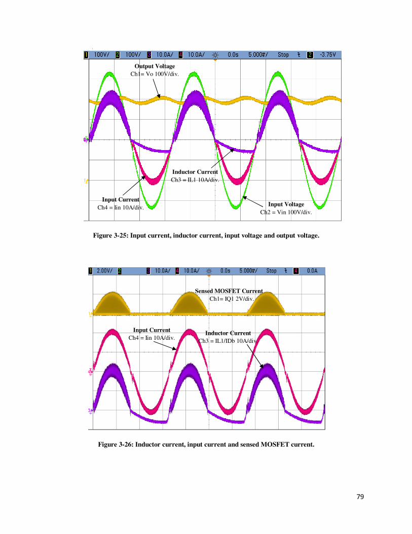
79
Figure 3-25: Input current, inductor current, input voltage and output voltage.
Figure 3-26: Inductor current, input current and sensed MOSFET current.
Input Voltage
Ch2 = Vin 100V/div.
Output Voltage Ch1= Vo 100V/div.
Inductor Current
Ch3 = IL1 10A/div.
Input Current
Ch4 = Iin 10A/div.
Sensed MOSFET Current Ch1= IQ1 2V/div.
Inductor Current
Ch3 = IL1/IDb 10A/div.
Input Current
Ch4 = Iin 10A/div.

80
Figure 3-27: Gating signal, inductor and sensed MOSFET current for D < 0.5
Figure 3-28: Gating signal, inductor and sensed MOSFET current for D > 0.5
Sensed MOSFET Current Ch2= IQ1 2V/div.
Inductor Current
Ch3 = IL1/IDb 10A/div.
Gating Signal
Ch1= Vg 10V/div.
Sensed MOSFET Current Ch2= IQ1 2V/div.
Inductor Current
Ch3 = IL1/IDb 10A/div.
Gating Signal
Ch1= Vg 10V/div.

81
Figure 3-29: Load transient response from NL to FL (0W to 3400 W)
Ch1= Vo 100V/div. Ch2= Iin 10A/div. Ch4= Vo 100V/div
Figure 3-30: Load transient response from FL to NL (3400 W to 0 W)
Ch1= Vo 100V/div. Ch2= Iin 10A/div. Ch4= Vo 100V/div

82
3.7. Conclusion
A new high performance phase shifted semi-bridgeless AC-DC Boost converter topology
has been presented in this chapter for the front-end AC-DC converter in PHEV battery chargers.
The proposed converter features high efficiency at light loads and low lines, which is critical to
minimize the charger size, charging time and the amount and cost of electricity drawn from the
utility; the component count, which reduces the charger cost; and reduced EMI. The converter is
ideally suited for automotive level 1 residential charging applications in North America where
the typical supply is limited to 120 V and 1.44 kVA.
An analysis and performance characteristics are presented. A breadboard converter circuit
has been built to verify the proof-of-concept. The theoretical waveforms were compared with the
results taken from prototype unit. Additionally, key experimental waveforms were provided and
input current harmonics at each harmonic order were compared more explicitly with the IEC
61000-3-2 standard limits.
Experimental results demonstrate that the mains current THD is smaller than 5% from
50% load to full load and the converter is compliant with the IEC 61000-3-2 standard. The
converter power factor was also provided for full power range at 120 and 240 V input. The
power factor is greater than 0.99 from 50% load to full load. The proposed converter achieves a
peak efficiency of 98.6 % at 240 V input and 1 kW output power.

83
CHAPTER 4. The Ripple Steering Technique and Converter
Modeling
4.1. Introduction
In this chapter, an average switch model approach to the power stage modeling, feedback
compensation, and dynamic analysis of PFC boost converters with coupled magnetic filter is
presented. The model is expressed by the derivation of power stage transfer functions for
conventional boost converter, and then followed by the power stage transfer functions for PFC
boost converter with coupled magnetic filters. Experimental and simulation results of a prototype
boost converter converting universal AC input voltage to 400 V DC at 1.8 kW are given to verify
the proof of concept, and analytical work reported in this chapter. The experimental result
demonstrates that the model can correctly predict the steady-state and large signal dynamic
behavior of a CCM PFC boost converter with coupled magnetic filter.
4.2. Average Switch Model
Using the model discussed in section 1.3.6 applying that to modified boost converter with
coupled inductors, any of the transfer functions between the output variables (output voltage and
inductor current) and the input variables (input voltage and duty ration) can be derived.
4.2.1. PWM Switch Model of Conventional Boost Converter
Applying the PWM switch model results in the equivalent circuit shown in Figure 4-1 for the
conventional boost converter:
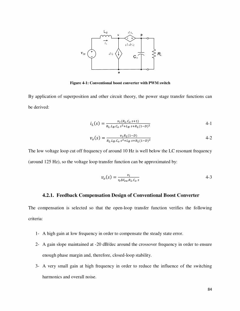
84
Figure 4-1: Conventional boost converter with PWM switch
By application of superposition and other circuit theory, the power stage transfer functions can
be derived:
;A$ >?.h .[= :-&h .Ai.[= :+-Ai :-h&,0+ 4-1
5$ >?.h&,0h .Ai.[= :+-Ai :-h&,0+ 4-2
The low voltage loop cut off frequency of around 10 Hz is well below the LC resonant frequency
(around 125 Hz), so the voltage loop transfer function can be approximated by:
5$ >?ɳ.∆kl.h .[= : 4-3
4.2.1. Feedback Compensation Design of Conventional Boost Converter
The compensation is selected so that the open-loop transfer function verifies the following
criteria:
1- A high gain at low frequency in order to compensate the steady state error.
2- A gain slope maintained at -20 dB/dec around the crossover frequency in order to ensure
enough phase margin and, therefore, closed-loop stability.
3- A very small gain at high frequency in order to reduce the influence of the switching
harmonics and overall noise.
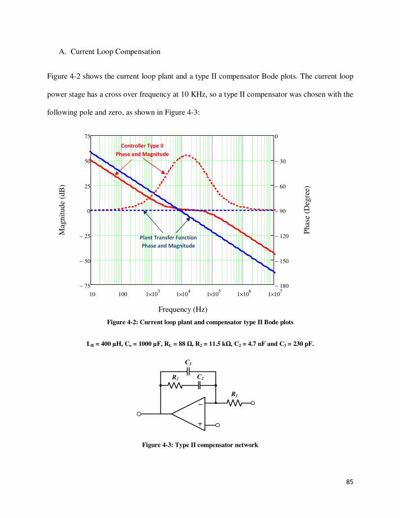
85
A. Current Loop Compensation
Figure 4-2 shows the current loop plant and a type II compensator Bode plots. The current loop
power stage has a cross over frequency at 10 KHz, so a type II compensator was chosen with the
following pole and zero, as shown in Figure 4-3:
Figure 4-2: Current loop plant and compensator type II Bode plots
LB = 400 µH, Co = 1000 µF, RL = 88 Ω, R2 = 11.5 kΩ, C2 = 4.7 nF and C3 = 230 pF.
C3
C2R2
R1
Figure 4-3: Type II compensator network
10 100 1 103
× 1 104
× 1 105
× 1 106
× 1 107
×
75−
50−
25−
0
25
50
75
180−
150−
120−
90−
60−
30−
0
Frequency (Hz)
Mag
nit
ude
(dB
)
Phas
e (D
egre
e)
Plant Transfer Function
Phase and Magnitude
Controller Type II
Phase and Magnitude
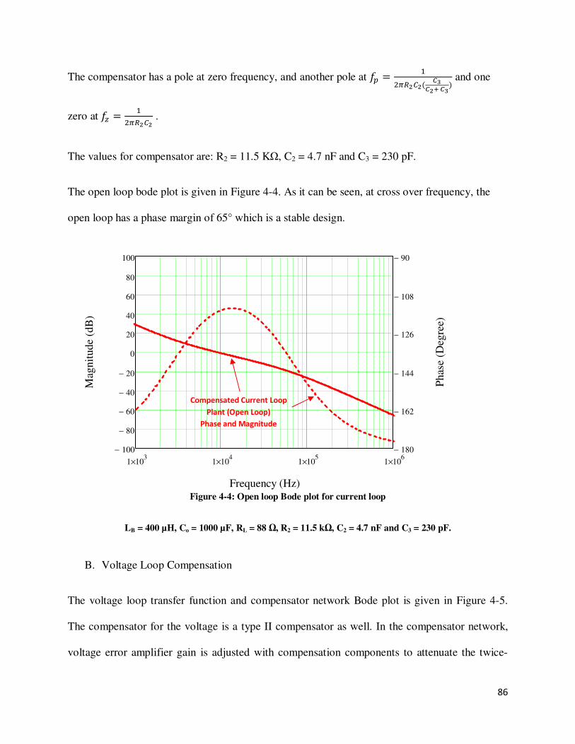
86
The compensator has a pole at zero frequency, and another pole at m &HP+[+ nEn+o nE and one
zero at mp &HP+[+ .
The values for compensator are: R2 = 11.5 KΩ, C2 = 4.7 nF and C3 = 230 pF.
The open loop bode plot is given in Figure 4-4. As it can be seen, at cross over frequency, the
open loop has a phase margin of 65° which is a stable design.
Figure 4-4: Open loop Bode plot for current loop
LB = 400 µH, Co = 1000 µF, RL = 88 Ω, R2 = 11.5 kΩ, C2 = 4.7 nF and C3 = 230 pF.
B. Voltage Loop Compensation
The voltage loop transfer function and compensator network Bode plot is given in Figure 4-5.
The compensator for the voltage is a type II compensator as well. In the compensator network,
voltage error amplifier gain is adjusted with compensation components to attenuate the twice-
1 103
× 1 104
× 1 105
× 1 106
×
100−
80−
60−
40−
20−
0
20
40
60
80
100
180−
162−
144−
126−
108−
90−
Frequency (Hz)
Mag
nit
ude
(dB
)
Phas
e (D
egre
e)
Compensated Current Loop
Plant (Open Loop)
Phase and Magnitude
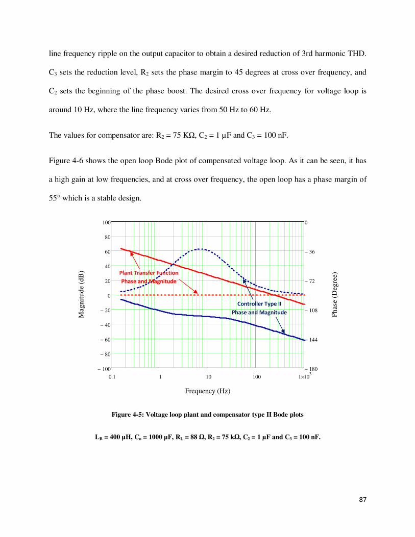
87
line frequency ripple on the output capacitor to obtain a desired reduction of 3rd harmonic THD.
C3 sets the reduction level, R2 sets the phase margin to 45 degrees at cross over frequency, and
C2 sets the beginning of the phase boost. The desired cross over frequency for voltage loop is
around 10 Hz, where the line frequency varies from 50 Hz to 60 Hz.
The values for compensator are: R2 = 75 KΩ, C2 = 1 µF and C3 = 100 nF.
Figure 4-6 shows the open loop Bode plot of compensated voltage loop. As it can be seen, it has
a high gain at low frequencies, and at cross over frequency, the open loop has a phase margin of
55° which is a stable design.
Figure 4-5: Voltage loop plant and compensator type II Bode plots
LB = 400 µH, Co = 1000 µF, RL = 88 Ω, R2 = 75 kΩ, C2 = 1 µF and C3 = 100 nF.
0.1 1 10 100 1 103
×
100−
80−
60−
40−
20−
0
20
40
60
80
100
180−
144−
108−
72−
36−
0
Frequency (Hz)
Mag
nit
ud
e (d
B)
Ph
ase
(Deg
ree)Plant Transfer Function
Phase and Magnitude
Controller Type II
Phase and Magnitude

88
Figure 4-6: Open loop Bode plot for voltage loop
LB = 400 µH, Co = 1000 µF, RL = 88 Ω, R2 = 75 kΩ, C2 = 1 µF and C3 = 100 nF.
4.3. Ripple Steering Techniques in PFC Application
Although the control strategy of PFC stage is similar to that of a conventional boost
converter, but their power stage transfer functions are different. And no modeling has been done
to verify the effect of added coupled filter to the power stage transfer functions, and thus the
design of feedback loop compensator.
Figure 4-7: Modified PFC boost converter with coupled inductors
0.1 1 10 100 1 103
×
100−
80−
60−
40−
20−
0
20
40
60
80
100
180−
153−
126−
99−
72−
45−
Frequency (Hz)
Mag
nit
ud
e (d
B)
Ph
ase
(Deg
ree)
Compensated Voltage Loop
Plant (Open Loop)
Phase and Magnitude

89
Application of PWM switch model discussed in section 1.3.6 is used for the circuit
shown in Figure 4-7 for boost converter with coupled inductors in order to get the voltage and
current plant transfer functions.
4.3.1. PWM Switch Model of Boost Converter with Coupled Inductor
In order to model the boost converter with coupled inductors, the winding arrangements
shown in Figure 4-8 can be described mathematically by:
5& q& 6 + r 6+ 4-4
5H qH 6+ + r 6 4-5
where: r s tq& qH 4-6
M is the mutual inductance and k is the coupling coefficient of the windings.
Figure 4-8: Equivalent circuit of coupled inductors
From above equations, Figure 4-8 can be replaced with its equivalent circuit shown in Figure 4-9
[71].
Figure 4-9: Equivalent circuit of coupled inductors
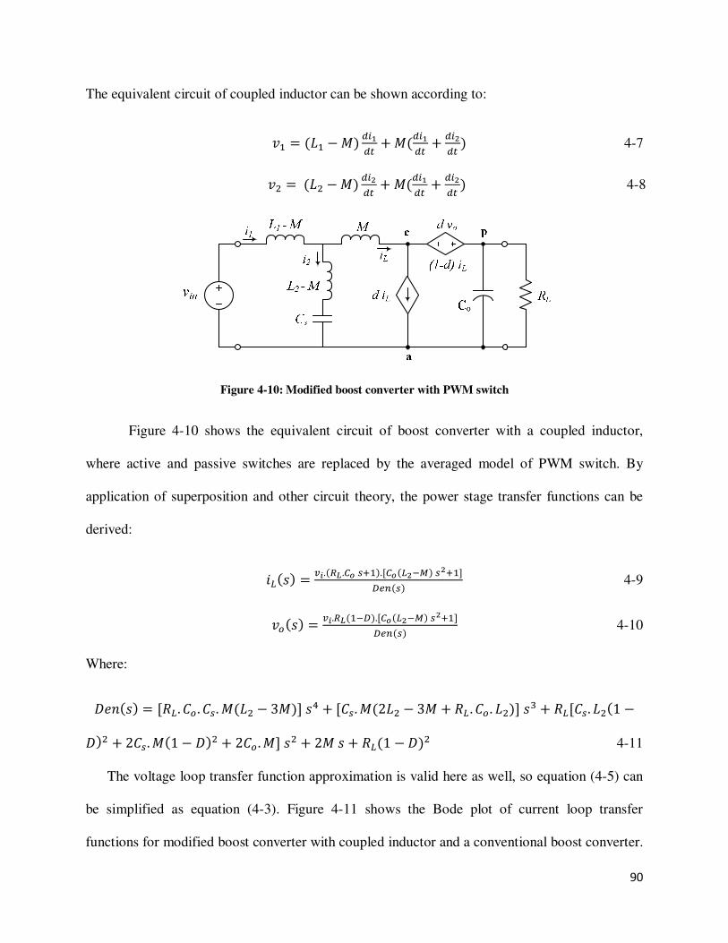
90
The equivalent circuit of coupled inductor can be shown according to:
5& q& − r 6 + r6 + 6+ 4-7
5H qH − r 6+ + r6 + 6+ 4-8
Figure 4-10: Modified boost converter with PWM switch
Figure 4-10 shows the equivalent circuit of boost converter with a coupled inductor,
where active and passive switches are replaced by the averaged model of PWM switch. By
application of superposition and other circuit theory, the power stage transfer functions can be
derived:
;A$ >?.h .[= :-&.[[=A+,v :+-&]0: 4-9
5$ >?.h&,0.[[=A+,v :+-&]0: 4-10
Where:
)<$ [xA. y . y:. rqH − 3r] $Z + [y:. r2qH − 3r + xA . y . qH] $D + xA[y:. qH1 −)H + 2y:. r1 − )H + 2y . r] $H + 2r $ + xA1 − )H 4-11
The voltage loop transfer function approximation is valid here as well, so equation (4-5) can
be simplified as equation (4-3). Figure 4-11 shows the Bode plot of current loop transfer
functions for modified boost converter with coupled inductor and a conventional boost converter.

91
As it can be noted, the phase margins for both plants are the same and steady at -90 °. But the
main difference is the magnitude of current plant transfer functions, where for conventional
boost has lower cross over frequency and lower gain. If the same feedback compensation
network is used for both converters, the steady state and large signal responses would not be
adequate.
Figure 4-11: Current loop plant Bode plots
LB = 400 µH, Co = 1000 µF, RL = 88 Ω, Ldc = 400 µH, Lac = 250 µH, M = 260 µH, Cs = 1 µF.
1 103
× 1 104
× 1 105
× 1 106
× 1 107
×
75−
50−
25−
0
25
50
75
180−
150−
120−
90−
60−
30−
0
Frequency (Hz)
Mag
nit
ud
e (d
B)
Ph
ase
(Deg
ree)
Conventional Boost
Plant Transfer Function
Phase and Magnitude
Modified Boost Plant
Transfer Function
Phase and Magnitude

92
4.3.1. Feedback Compensation Design of Boost Converter with Coupled
Inductor
Figure 4-12 shows the current loop plant and a type II compensator Bode plots. The
current loop power stage has a cross over frequency at 20 KHz, so a type II compensator was
chosen with the following pole and zero: pole at m &HP+[+ nEn+o nE and one zero at mp &HP+[+ .
The values for compensator are: R2 = 22.1 KΩ, C2 = 1 nF and C3 = 150 pF.
The open loop Bode plot is given in Figure 4-13. As it can be seen, at the cross over frequency,
the open loop has a phase margin of 50° which is a stable design.
Figure 4-12: Current loop plant and compensator Bode plots for boos converter with coupled inductor
RL = 88 Ω, Ldc = 400 µH, Lac = 250 µH, M = 260 µH, Cs = 1 µF, R2 = 22.1 kΩ, C2 = 1 nF and C3 = 150 pF.
10 100 1 103
× 1 104
× 1 105
× 1 106
× 1 107
×
50−
25−
0
25
50
75
100
180−
150−
120−
90−
60−
30−
0
Frequency (Hz)
Mag
nit
ud
e (d
B)
Ph
ase
(Deg
ree)
Modified boost Plant
Transfer Function
Phase and Magnitude
Controller Type II
Phase and Magnitude
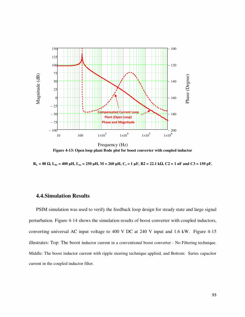
93
Figure 4-13: Open loop plant Bode plot for boost converter with coupled inductor
RL = 88 Ω, Ldc = 400 µH, Lac = 250 µH, M = 260 µH, Cs = 1 µF, R2 = 22.1 kΩ, C2 = 1 nF and C3 = 150 pF.
4.4. Simulation Results
PSIM simulation was used to verify the feedback loop design for steady state and large signal
perturbation. Figure 4-14 shows the simulation results of boost converter with coupled inductors,
converting universal AC input voltage to 400 V DC at 240 V input and 1.6 kW. Figure 4-15
illustrates: Top: The boost inductor current in a conventional boost converter - No Filtering technique.
Middle: The boost inductor current with ripple steering technique applied, and Bottom: Series capacitor
current in the coupled inductor filter.
10 100 1 103
× 1 104
× 1 105
× 1 106
×
100−
75−
50−
25−
0
25
50
75
100
125
150
200−
180−
160−
140−
120−
100−
Frequency (Hz)
Mag
nit
ude
(dB
)
Phas
e (D
egre
e)
Compensated Current Loop
Plant (Open Loop)
Phase and Magnitude
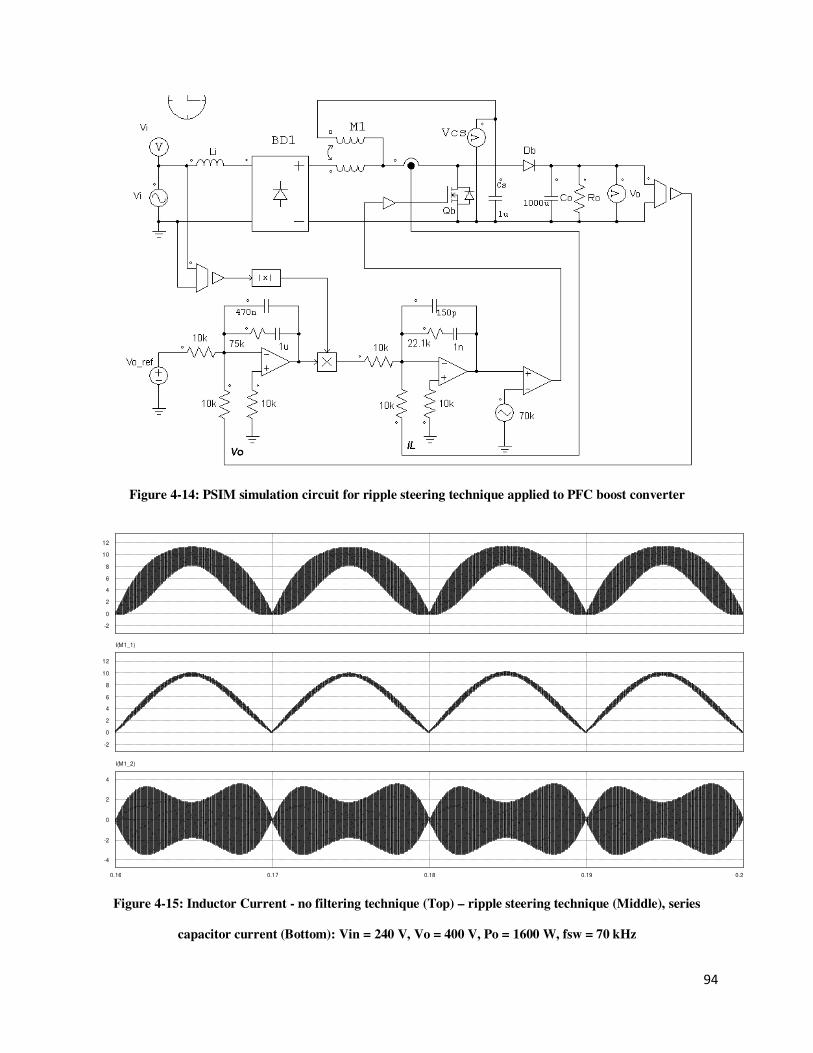
94
Figure 4-14: PSIM simulation circuit for ripple steering technique applied to PFC boost converter
Figure 4-15: Inductor Current - no filtering technique (Top) – ripple steering technique (Middle), series
capacitor current (Bottom): Vin = 240 V, Vo = 400 V, Po = 1600 W, fsw = 70 kHz
0
-2
2
4
6
8
10
12
0
-2
2
4
6
8
10
12
I(M1_1)
0.16 0.17 0.18 0.19 0.2
0
-2
-4
2
4
I(M1_2)
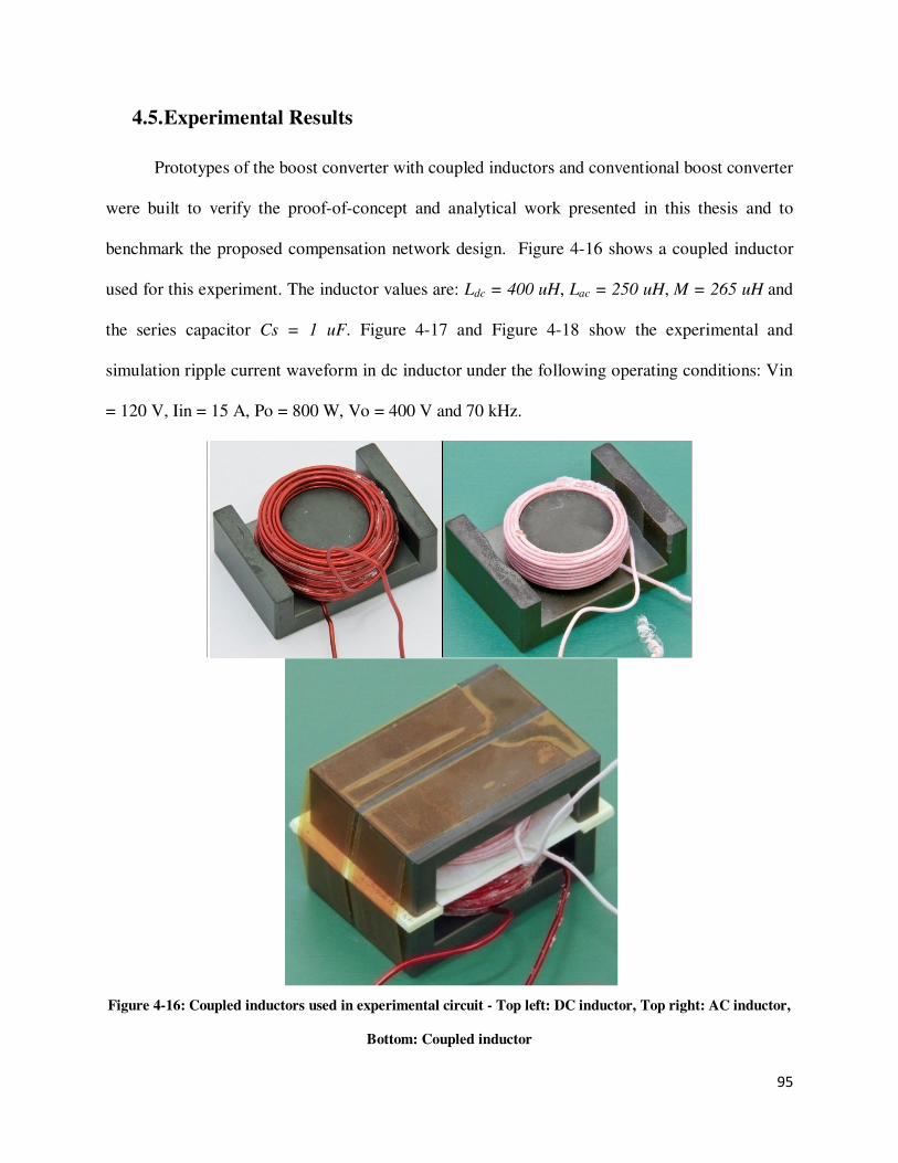
95
4.5. Experimental Results
Prototypes of the boost converter with coupled inductors and conventional boost converter
were built to verify the proof-of-concept and analytical work presented in this thesis and to
benchmark the proposed compensation network design. Figure 4-16 shows a coupled inductor
used for this experiment. The inductor values are: Ldc = 400 uH, Lac = 250 uH, M = 265 uH and
the series capacitor Cs = 1 uF. Figure 4-17 and Figure 4-18 show the experimental and
simulation ripple current waveform in dc inductor under the following operating conditions: Vin
= 120 V, Iin = 15 A, Po = 800 W, Vo = 400 V and 70 kHz.
Figure 4-16: Coupled inductors used in experimental circuit - Top left: DC inductor, Top right: AC inductor,
Bottom: Coupled inductor

96
Figure 4-17: Inductor current Idc ripple at 120 V input and 800 W output - Experimental
Figure 4-18: Inductor current Idc ripple at 120 V input and 800 W output - Simulation
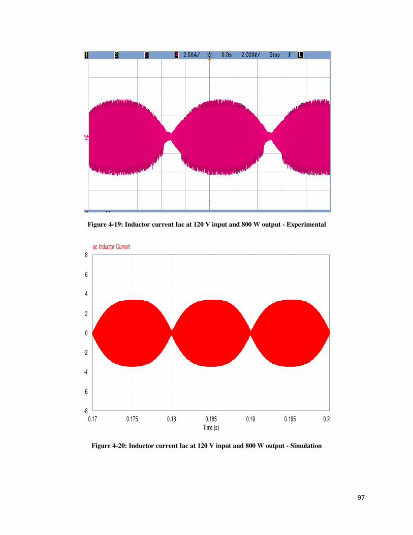
97
Figure 4-19: Inductor current Iac at 120 V input and 800 W output - Experimental
Figure 4-20: Inductor current Iac at 120 V input and 800 W output - Simulation
0.17 0.175 0.18 0.185 0.19 0.195 0.2
Time (s)
0
-2
-4
-6
-8
2
4
6
8ac Inductor Current

98
Figure 4-21: Peak inductor current Iac ripple at 120 V input and 800 W output - Experimental
Figure 4-22: Peak inductor current Iac ripple at 120 V input and 800 W output - Simulation

99
Figure 4-23: Inductor current Idc ripple at 240 V input and 1600 W output - Experimental
Figure 4-24: Inductor current Idc ripple at 240 V input and 1600 W output - Simulation
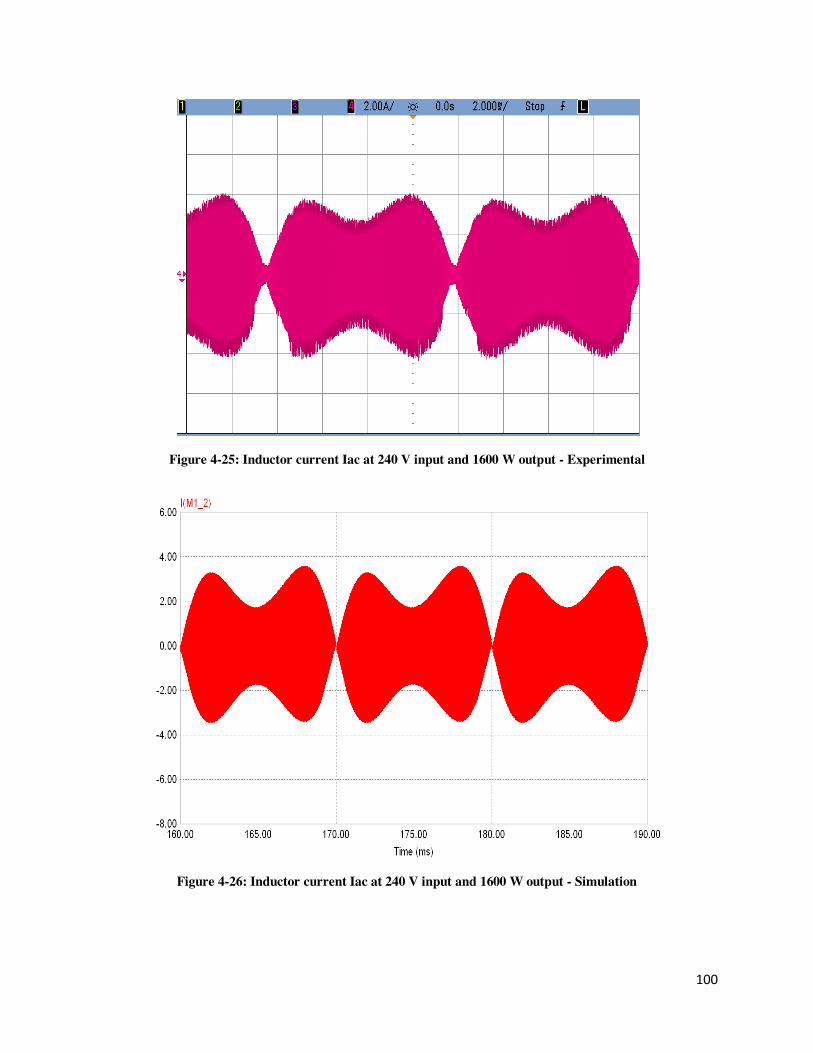
100
Figure 4-25: Inductor current Iac at 240 V input and 1600 W output - Experimental
Figure 4-26: Inductor current Iac at 240 V input and 1600 W output - Simulation

101
Figure 4-27: Peak inductor current Iac ripple at 240 V input and 1600 W output - Experimental
Figure 4-28: Peak inductor current Iac ripple at 240 V input and 1600 W output - Simulation

102
Figure 4-19 and Figure 4-20 show the experimental and simulation current waveforms in ac
inductor under the following operating conditions: Vin = 120 V, Iin = 15 A, Po = 800 W, Vo =
400 V and 70 kHz. Figure 4-21 and Figure 4-22 show the experimental and simulation ripple
current waveforms in ac inductor under the same operating conditions as above.
Figure 23 through Figure 28 repeats the same waveforms for different test condition: Vin =
240 V, Iin = 15 A, Po = 1600 W, Vo = 400 V and 70 kHz.
4.6. Conclusion
An averaged PWM model for boost converters with ripple steering technique has been
developed and effect of ripple steering technique on properly design of compensation network
for the current loop has been studied. The analytical and simulation results were compared with
experimental results of a breadboard converter circuit converting universal AC input voltage to
400 V DC at 240 V input and 1.6 kW. The proposed model shows an accurate prediction of
steady state and large transient behavior of boost converter with coupled inductors.

103
CHAPTER 5. Conclusions and Future Work
5.1. Conclusions
As the adaptation rate of PHEVs increases, the stress on the utility grid is projected to
increase significantly at times of peak demand. Therefore, efficient and high power factor
charging is critical in order to minimize the utility load stress, and reduce the charging time. In
addition, a high power factor is needed to limit the input current harmonics drawn by these
chargers and to meet regulatory standards.
To meet the next generation requirements of these applications, two new topologies and
two new modeling techniques have been proposed in this thesis.
5.1.1. Bridgeless Interleaved Boost PFC Converter
The first contribution is a new bridgeless interleaved boots PFC converter for plug in
hybrid electric vehicle level 2 charger applications. The proposed topology achieves a peak
efficiency of 98.94% was reached at 265 V input and 1.2 kW output power. High efficiency over
the entire load range is achieved in this topology, enabling fewer problems with heat dissipation
and cooling systems. Furthermore, a higher efficiency means more power is available from the
mains feed to charge the batteries, reducing charging times and electricity costs.
5.1.2. Phase Shifted Semi-Bridgeless Boost PFC Converter
The second contribution is a new phase shifted semi-bridgeless boost PFC converter for
plug in hybrid electric vehicle level 1 charger applications. Experimental results demonstrate that
the mains current THD is smaller than 5% from 50% load to full load and the converter is
compliant with the IEC 61000-3-2 standard. The converter power factor was also provided for

104
full power range at 120 and 240V input. The power factor is greater than 0.99 from 50% load to
full load. The proposed converter achieves a peak efficiency of 98.6 % at 240 V input and 1 kW
output power.
5.1.3. New Loss Modeling for PFC Boost Converters
In order to properly select the power stage components of a converter and calculate the
associated power losses, it is necessary to determine the RMS and average values of their
currents. In a typical boost converter, the MOSFET and diode current waveforms are pulsed-
width modulated, with both the duty cycle and peak amplitude varying with the AC input. And
without an effective mathematical method for computing these RMS and average values, the
proper design and selection of power stage components can be flawed. A new analytical model
for the four different topologies was developed, enabling the calculation of power losses and
efficiency calculation.
5.1.1. New Average Modeling for PFC Boost Converters with Coupled
Inductors
An averaged PWM model for boost converters with ripple steering technique has been
developed and effect of ripple steering technique on properly design of compensation network
for current loop has been studied. The analytical and simulation results were compared with
experimental results of a breadboard converter circuit converting universal AC input voltage to
400 V DC at 240 V input and 1.8 kW. The proposed model shows an accurate prediction of the
steady state and large transient behavior of boost converter with coupled inductor.

105
5.2. Future Work
This sub-section outlines the possible future work for the thesis topics.
5.2.1. LLC Resonant Converter for DC/DC Stage
The front end PFC section of a PHEV charger is followed by a DC/DC section to
complete the charger system. This stage can be an LLC resonant converter. High efficiency (>
98%), high output voltage (~ 450 V), high power (~ 3.3 KW) and wide output voltage range (220
V to 450 V) makes it a challenging research topic.
5.2.2. Resonant PFC Converter
Most of hard switching PFC boost topologies have been discussed in this dissertation, but
a new class of topology for PFC is resonant PFC converters. Recent research activities have been
conducted by Infineon Technology on Bridgeless Interleaved resonant PFC and also by Dr.
Slobodan Ćuk from TESLAco on Bridgeless Resonant PFC.
5.2.3. Level 3 Chargers
With cities having it mandatory to have a Level 3 charger installed in every high rise build
in the lower main island in a near future, the business case is already justified.
The ultimate in charge technology, but nobody has yet really settled on a standard, leaving
manufacturers of cars and charging equipment to come up with their own. This type of charging
is defined as any charging above 14.4 kilowatts. Also, most Level 3 stations are considered “fast
chargers,” but they don’t have to be. The conventional wisdom is that if an average EV battery
can be charged to full in about a half hour, then it is a fast charge.
Interleaved resonant PFC and also by Dr. Slobodan Ćuk from TESLAco on Bridgeless

106
5.2.4. Wireless Chargers
Wireless charger is another interesting topic for future research. Several companies are
investing to develop a family of wireless electric power components that will enable OEM’s in a
broad range of industries and applications to make their products truly “wireless.” Wireless
electric power delivered over room scale distances, and with high efficiency. Wireless electric
power that is safe for people and animals. This might be the future of EV and PHEV chargers.

107
Bibliography
[1] K. Morrow ; D. Karner ; J. Francfort, "Plug-in Hybrid Electric Vehicle Charging Infrastructure
Review," U.S. Departent of Energy - Vehicle Technologies Program, 2008.
[2] "Compliance testing to the IEC 1000-3-2 (EN 61000-3-2) and IEC 1000-3-3 (EN 61000-3-3)
Standards ": Agilent Technology.
[3] A. F. Lisheng Shi; Meintz, M.; , "Single-Phase Bidirectional AC-DC Converters for Plug-in Hybrid
Electric Vehicle Applications," IEEE Vehicle Power and Propulsion Conference, VPPC, pp. 1 - 5
2008.
[4] http://www.eere.energy.gov/, "US Department of Energy - The Office of Energy Efficiency and
Renewable Energy (EERE)."
[5] B. Singh ; B.N. Singh ; A. Chandra ; K. Al-Haddad ; A. Pandey ; D.P. Kothari, "A Review of Single-
Phase Improved Power Quality AC-DC Converters," IEEE Transactions on Industrial Electronics,
vol. 50, pp. 962 - 981, 2003.
[6] C. Qiao ; K.M. Smedley, "A Topology Survey of Single-Stage Power Factor Corrector with a Boost
Type Input-Current-Shaper," IEEE Transactions on Power Electronics, vol. 16, pp. 360 - 368, 2001.
[7] D. Tollik ; A. Pietkiewicz, "Comparative analysis of 1-phase active power factor correction
topologies," in IEEE Telecommunications Energy Conference, INTELEC, 1992, pp. 517 - 523
[8] L. Petersen ; M. Andersen, "Two-Stage Power Factor Corrected Power Supplies: The Low
Component-Stress Approach " in IEEE Applied Power Electronics Conference and Exposition,
APEC. vol. 2, 2002, pp. 1195 - 1201.
[9] T.S. Key ; Jih-Sheng Lai, "IEEE and International Harmonic Standards Impact on Power Electronic
Equipment Design," in International Conference on Industrial Electronics, Control and
Instrumentation, IECON. vol. 2, 1997, pp. 430 - 436.
[10] Ned Mohan ; Tore M. Undeland, Power electronics: converters, applications, and design: Wiley
India, 2009.
[11] "IEEE Std 519-1992 IEEE Recommended Practices and Requirements for Harmonic Control in
Electrical Power Systems," IEEE 1992.
[12] "Guide to Energy Management - Power Factor," BC Hydro, Vancouver 2000.
[13] L. Huber ; Liu Gang ; M.M. Jovanovic, "Design-Oriented Analysis and Performance Evaluation of
Buck PFC Front End," vol. 25, pp. 85 - 94, 2010.
[14] A. Fernandez ; J. Sebastian ; M.M. Hernando ; P. Villegas ; J. Garcia, "Helpful Hints to Select a
Power-Factor-Correction Solution for Low- and Medium-Power Single-Phase Power Supplies,"
IEEE Transactions on Industrial Electronics, vol. 52, pp. 46 - 55 2005.
[15] J. M. Bourgeois, "CIRCUITS FOR POWER FACTOR CORRECTION WITH REGARDS TO MAINS
FILTERING," STMicroelectronics 1999.
[16] R. Randall, "Choosing Power Switching Devices for SMPS Designs MOSFETs or IGBTs?," Fairchild
Semiconductor Application Note AN-7010 2005.
[17] L. Rossetto ; G. Spiazzi ; P. Tenti, "CONTROL TECHNIQUES FOR POWER FACTOR CORRECTION
CONVERTERS."
[18] W. Z. G. F. Y.-F. L. B. Wu;, "A Digital Power Factor Correction (PFC) Control Strategy Optimized
for DSP," IEEE Transactions on Power Electronics vol. 19, pp. 1474 - 1485, 2004.
[19] P. N. Sangsun Kim; Enjeti, "Control of Multiple Single-Phase PFC Modules With a Single Low-Cost
DSP," IEEE Transactions on Industry Applications, vol. 39, pp. 1379 - 1385 2003.
[20] M. C. J. Sun;, "Feedforward current control of boost single-phase PFC converters," IEEE
Transactions onPower Electronics, vol. 21, pp. 338 - 345, 2006.

108
[21] A. J. S. Min Chen; Mathew, "Nonlinear Current Control of Single-Phase PFC Converters," Power
Electronics, IEEE Transactions on vol. 22, pp. 2187 - 2194, 2007.
[22] Y. Chen ; D. He ; R.M. Nelms, "Control of a Single-Phase PFC Preregultaor using an 8-bit
Microcontroller," in IEEE Applied Power Electronics Conference, APEC, 2007, pp. 1454 - 1460
[23] P. Grasblum, "Implementing PFC Average Current Mode Control using the MC9S12E128,"
Freescale Semiconductor Application Note AN3052 2005.
[24] "Implementing a Digital AC/DC Switched-Mode Power Supply using a 56F8300 Digital Signal
Controller," Freescale Semiconductor Application Note AN3115 2005.
[25] G. Chu ; S.C. Tan ; C.K. Tse ; S.C. Wong, "General Control for Boost PFC Converter from a Sliding
Mode Viewpoint," in IEEE Power Electronics Specialists Conference, PESC, 2008, pp. 4452 - 4456.
[26] Y. Z. W. X. Y. Yu;, "The PFC with Average Current-Mode and Voltage Fuzzy Controller for the
Output Voltage," in International Symposium on Intelligent Information Technology
Application,IEEE IITA, 2008, pp. 771 - 775.
[27] J.M. Carrasco ; J.M. Quero ; F.P. Ridao ; M.A. Perales ; L.G. Franquelo, "Sliding Mode Control of a
DC-DC PWM Converter with PFC Implemented by Neural Netwroks," IEEE Transactions on
Circuits and Systems I: Fundamental Theory and Applications, vol. 44, pp. 743 - 749 1997.
[28] K. M. Zheren Lai; Smedley, "A Family of Continuous-Conduction-Mode Power-Factor-Correction
Controllers Based on the General Pulse-Width Modulator," IEEE Transactions on Power
Electronics, vol. 13, pp. 501 - 510 1998
[29] S. Basu ; T.M. Undeland, "Inductor Design Considerations for optimizing performance & cost of
Continuous Mode Boost PFC Converters," in IEEE Applied Power Electronics Conference and
Exposition, APEC. vol. 2, 2005, pp. 1133 - 1138.
[30] L. Dixon, "Average Current Mode Control of Switching Power Supplies," UNITRODE
CORPORATION Application Note SLUP091 1990.
[31] E. Najafi ; A. Vahedi ; A. Mahanfar ; A. Yatim, "A new controlling method based on peak current
mode (PCM) for PFC," in IEEE Power and Energy Conference, PECon, 2008, pp. 1103 - 1107
[32] C. Zhou ; R.B. Ridley ; F.C. Lee, "Design and Analysis of a Hysteretic Boost Power Factor
Correction Circuit," in IEEE Power Electronics Specialists Conference, PESC, 1990, pp. 800 - 807.
[33] J. P. Noon, "Designing High-Power Factor Off-Line Power Supplies," Texas Instruments
Application Note SLUP203 2003.
[34] P. C. Todd, "UC3854 Controlled Power Factor Correction Circuit Design," Unitrode APPLICATION
NOTE SLUA 144 1999.
[35] E.M Hertz ; S. Busquets-Monge ; D. Boroyevich ; M. Arpilliere ; H. Boutillier, "Analysis of the
Trade-offs between Thermal Behavior and EMI Noise Levels in a Boost PFC Circuit," in IEEE
Industry Applications Conference, IAS. vol. 4, 2001, pp. 2460 - 2465.
[36] F. C. O. Shuo Wang; Lee, W.G.; , "Characterization, Evaluation, Design of Noise Separator for
Conducted EMI Noise Diagnosis," IEEE Transactions on Power Electronics vol. 20, pp. 974 - 982
2005.
[37] F. C. Shuo Wang; Pengju Kong; Lee, "Common Mode Noise Reduction for Boost Converters Using
General Balance Technique," IEEE Transactions on Power Electronics, vol. 22, pp. 1410 - 1416
2007.
[38] M. T. L. Wei Zhang; Zhang, F.C.; Roudet, J.; Clavel, E.; , "Conducted EMI Analysis of a Boost PFC
Circuit," in IEEE Applied Power Electronics Conference and Exposition, APEC. vol. 1, 1997, pp. 223
- 229.
[39] L. Rossetto ; S. Buso ; G. Spiazzi, "Conducted EMI issues in a 600-W single-phase boost PFC
design," IEEE Transactions on Industry Applications, vol. 36, pp. 578 - 585 2000.
[40] F. Beltrame ; L. Roggia ; A. da Rosa Abaide ; L. Schuch ; J.R. Pinheiro, "EMI Investigation Yield by
Single-Phase PFC Pre-Regulators," in IEEE Industrial Electronics, IECON, 2009, pp. 4128 - 4133

109
[41] B. Lu ; W. Dong ; S. Wang ; F.C. Lee, "High frequency investigation of single-switch CCM power
factor correction converter," in IEEE Applied Power Electronics Conference and Exposition, APEC.
vol. 3, 2004, pp. 1481 - 1487.
[42] F. C. Pengju Kong; Shuo Wang; Lee, "Improving Balance Technique for High Frequency Common
Mode Noise Reduction in Boost PFC Converters," in IEEE Power Electronics Specialists
Conference, PESC, 2008, pp. 2941 - 2947
[43] F. C. O. Shuo Wang; Lee, W.G.; , "Improving the Performance of Boost PFC EMI Filter," in IEEE
Applied Power Electronics Conference and Exposition, APEC. vol. 1, 2003, pp. 368 - 374.
[44] F. C. O. Liyu Yang; Bing Lu; Wei Dong; Zhiguo Lu; Ming Xu; Lee, W.G.; , "Modeling and
Characterization of a 1KW CCM PFC Converter for Conducted EMI Prediction," in IEEE Applied
Power Electronics Conference and Exposition, APEC. vol. 2, 2004, pp. 763 - 769.
[45] C. Wang ; M. Xu ; B. Lu ; F.C. Lee, "New Architecture for MHz Switching Frequency PFC," in IEEE
Applied Power Electronics Conference, APEC, 2007, pp. 179 - 185
[46] F.C. Lee ; Shuo Wang ; Pengju Kong ; Chuanyun Wang ; Dianbo Fu, "Power architecture design
with improved system efficiency, EMI and power density," in IEEE Power Electronics Specialists
Conference, PESC, 2008, pp. 4131 - 4137.
[47] F. C. Dehong Xu; Jindong Zhang; Weiyun Chen; Jinjun Lin; Lee, "Evaluation of output filter
capacitor current ripples in single phase PFC converters " in Proceedings of the Power
Conversion Conference, PCC. vol. 3 Osaka, Japan, 2002, pp. 1226 - 1231.
[48] D. Mitchell, "AC–DC converter having an improved power factor," United States, 1983.
[49] W.-Y. C. J.-M. K. E.-H. K. J.-J. L. B.-H. Kwon;, "Bridgeless Boost Rectifier With Low Conduction
Losses and Reduced Diode Reverse-Recovery Problems," IEEE Transactions on Industrial
Electronics, vol. 54, pp. 769 – 780, April 2007 2007.
[50] M. M. D. Yungtaek Jang; Jovanovic, D.L.;, "Bridgeless PFC boost rectifier with optimized
magnetic utilization," in IEEE Applied Power Electronics Conference and Exposition, 2008, pp.
1017 – 1021.
[51] J. M. Hancock, "Bridgeless PFC Boosts Low-Line Efficiency," Infineon Technologies, 2008.
[52] U. Moriconi, "A Bridgeless PFC Configuration based on L4981 PFC Controller ":
STMicroelectronics Application Note AN1606, 2002.
[53] B. Lu ; R. Brown ; M. Soldano, "Bridgeless PFC implementation using one cycle control
technique," in IEEE Applied Power Electronics Conference and Exposition. vol. 2, 2005, pp. 812 -
817.
[54] F. C. Pengju Kong; Shuo Wang; Lee, "Common Mode EMI Noise Suppression for Bridgeless PFC
Converters," IEEE Transactions on Power Electronics, vol. 23, pp. 291 – 297, January 2008 2008.
[55] M. M. Yungtaek Jang; Jovanovic, "A Bridgeless PFC Boost Rectifier With Optimized Magnetic
Utilization," IEEE Transactions on Power Electronics, vol. 24, pp. 85 - 93 2009.
[56] C. Petrea ; M. Lucanu, "Bridgeless Power Factor Correction Converter Working at High Load
Variations," in International Symposium on Signals, Circuits and Systems, ISSCS. vol. 2, 2007, pp.
1 - 4
[57] L. Huber ; J. Yungtaek ; M.M. Jovanovic, "Performance Evaluation of Bridgeless PFC Boost
Rectifiers," IEEE Transactions on Power Electronics, vol. 23, pp. 1381 - 1390 2008.
[58] W. R. Frank, M.; Schlenk, M.; , "New Control Methods for Rectifier-Less PFC-Stages," in IEEE
International Symposium on Industrial Electronics, ISIE. vol. 2, 2005, pp. 489 - 493.
[59] M. A. E. T. Qingnan Li; Andersen, O.C.; , "Conduction losses and common mode EMI analysis on
bridgeless power factor correction " in International Conference on Power Electronics and Drive
Systems, PEDS, 2009, pp. 1255 - 1260
[60] P. Kong ; S. Wang ; F.C. Lee, "Common Mode EMI Noise Suppression for Bridgeless PFC
Converters," IEEE Transactions on Power Electronics, vol. 23, pp. 291 – 297, January 2008 2008.

110
[61] M. M. Yungtaek Jang; Jovanovic, "Interleaved Boost Converter With Intrinsic Voltage-Doubler
Characteristic for Universal-Line PFC Front End," IEEE Transactions on Power Electronics, vol. 22,
pp. 1394 – 1401, July 2007 2007.
[62] M. O’Loughlin;, "An Interleaved PFC Preregulator for High-Power Converters." vol. Topic 5: Texas
Instrument Power Supply Design Seminar, 2007, pp. 5-1, 5-14.
[63] L. Balogh ; R. Redl, "Power-factor correction with interleaved boost converters in continuous-
inductor-current mode," in IEEE Applied Power Electronics Conference and Exposition, 1993, pp.
168 - 174
[64] A. Jinsong Zhu; Pratt, "Capacitor ripple current in an interleaved PFC converter," in IEEE Power
Electronics Specialists Conference, 2008, pp. 3444 – 3450.
[65] F. C. Chuanyun Wang; Ming Xu; Lee, "Asymmetrical interleaving strategy for multi-channel PFC,"
in IEEE Applied Power Electronics Conference and Exposition, 2008, pp. 1409 - 1415.
[66] K. Raggl ; T. Nussbaumer ; G. Doerig ; J. Biela ; J.W. Kolar, "Comprehensive Design and
Optimization of a High Power Density Single-Phase Boost PFC," IEEE Transactions on Industrial
Electronics, vol. 56, pp. 2574 - 2587 2009.
[67] M.A.P. Andrade ; L. Schuch ; J.R. Pinheiro, "Generalized Switching Logic Scheme For CCM-PFC
Interleaved Boost Converters," in IEEE Power Electronics Specialists Conference, PESC. vol. 3,
2004, pp. 2353 - 2359.
[68] F. C. C. W. Pengju Kong; Shuo Wang; Lee, "Common-Mode EMI Study and Reduction Technique
for the Interleaved Multichannel PFC Converter," IEEE Transactions on Power Electronics, vol.
23, pp. 2576 - 2584 2008.
[69] F. C. B. L. Chuanyun Wang; Ming Xu; Lee, "EMI Study for the Interleaved Multi-Channel PFC," in
IEEE Power Electronics Specialists Conference, PESC, 2007, pp. 1336 - 1342
[70] D.C. Hamill ;P.T.Krein, "A `zero' ripple technique applicable to any DC converter " in IEEE Power
Electronics Specialists Conference, PESC. vol. 2, 1999, pp. 1165 - 1171.
[71] J.W. Kolar ; H. Sree ; N. Mohan ; F.C. Zach, "Novel aspects of an application of `zero'-ripple
techniques to basic converter topologies " in Power Electronics Specialists Conference, PESC. vol.
1, 1997, pp. 796 - 803.
[72] N.K. Poon ; J.C.P. Liu ; C.K. Tse ; M.H. Pong, "Techniques for input ripple current cancellation:
classification and implementation," IEEE Transactions on Power Electronics, vol. 15, pp. 1144 -
1152 2000.
[73] J. Wang ; W.G. Dunford ; K. Mauch, "Analysis of a ripple-free input-current boost converter with
discontinuous conduction characteristics " IEEE Transactions on Power Electronics, vol. 12, pp.
684 - 694, 1997.
[74] E. Chou ; F. Chen; C. Adragna ; B. Lu, "Ripple steering AC-DC converters to minimize input filter "
in IEEE Energy Conversion Congress and Exposition, ECCE, 2009, pp. 1325 - 1330.
[75] V. Vorperian, "Simplified analysis of PWM converters using model of PWM switch, Part I:
Continuous conduction mode " IEEE Transactions on Aerospace and Electronic Systems, vol. 26,
pp. 490 - 496 1990.
[76] V. Vorperian, "Simplified analysis of PWM converters using model of PWM switch, Part II:
Discontinuous conduction mode," IEEE Transactions on Aerospace and Electronic Systems, vol.
26, pp. 497 - 505 1990.
[77] F. Musavi ; K. Al-Haddad ; H.Y. Kanaan, "A large signal averaged modelling and control of
paralleled DC/DC converters with automatic load sharing," in IEEE Applied Power Electronics
Conference and Exposition, APEC. vol. 2, 2005, pp. 1353 - 1358.
[78] E. Van Dijk ; J.N. Spruijt ; D.M. O'Sullivan ; J.B. Klaassens, "PWM-switch modeling of DC-DC
converters " IEEE Transactions on Power Electronics, vol. 10, pp. 659 - 665 1995.

111
[79] Y.W. Lu ; W. Zhang ; Yanfei Liu, "A large signal dynamic model for single-phase AC-to-DC
converters with power factor correction " IEEE Power Electronics Specialists Conference, PESC,
vol. 2, pp. 1057 - 1063, 2004.
[80] Yan-Fei Liu ; P.C. Sen, "Large-signal modeling of hysteretic current-programmed converters "
IEEE Transactions on Power Electronics, vol. 11, pp. 423 - 430, 1996.
[81] Byungcho Choi ; Sung-Soo Hong ; Hyokil Park, "Modeling and small-signal analysis of controlled
on-time boost power-factor-correction circuit " IEEE Transactions on Industrial Electronics, vol.
48, pp. 136 - 142, 2001.
[82] F. Musavi ; W. Eberle ; W.G. Dunford, "A High-Performance Single-Phase AC-DC Power Factor
Corrected Boost Converter for plug in Hybrid Electric Vehicle Battery Chargers," in IEEE Energy
Conversion Congress and Exposition Atlanta, Georgia, 2010.
[83] F.Musavi ; W. Eberle ; W.G. Dunford, "Efficiency Evaluation of Single-Phase Solutions for AC-DC
PFC Boost Converters for Plug-in-Hybrid Electric Vehicle Battery Chargers," in IEEE Vehicle Power
and Propulsion Conference Lille, France, 2010.
[84] F.Musavi ; W. Eberle ; W.G. Dunford, "A Phase Shifted Semi-Bridgeless Boost Power Factor
Corrected Converter for Plug in Hybrid Electric Vehicle Battery Chargers," in IEEE Applied Power
Electronics Conference and Exposition, APEC Fort Worth, TX, 2011.

112
Appendix
MathCAD Simulation:
Power Component Selection, Magnetic Design and Compensator Network
Design
Part 1 - Power Component Selection
Design Variables Definition
Line Frequency
Minimum Input Voltage
Maximum Input Voltage
High Line Input Voltage
Low Line Input Voltage
Converter Effeciency at High Line
Converter Effeciency at Low Line
Maximum RMS Input Current
Maximum Input Power at High Line
Maximum Input Power at Low Line
Maximum Output Power at High Line
Maximum Output Power at Low Linw
Boost Output Voltage
Minimum Switching Frequency
Maximum boost ripple current as a percentage
Boost FET duty Cycle:
fin 50:=
Vinmin 85:=
Vinmax 265:=
VinHL 230:=
VinLL 115:=
η1 0.985:=
η2 0.965:=
Iin 16:=
Pin1 Iin VinHL⋅:=
Pin2 Iin VinLL⋅:=
Pout1 Pin1 η1⋅:= Pout1 3.625 103
×=
Pout2 Pin2 η2⋅:= Pout2 1.776 103
×=
Vboost 400:=
fs 175 103
⋅:=
∆Irp 50:=
δF_LL θ( ) 12 Vinmin⋅
Vboostsin θ( )⋅−:= δF_HL θ( ) 1
2 Vinmax⋅
Vboostsin θ( )⋅−:=
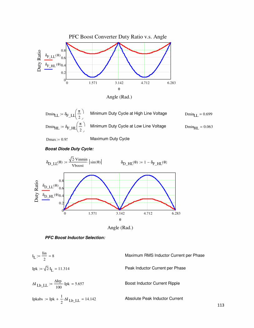
113
Minimum Duty Cycle at High Line Voltage
Minimum Duty Cycle at Low Line Voltage
Maximum Duty Cycle
Boost Diode Duty Cycle:
PFC Boost Inductor Selection:
Maximum RMS Inductor Current per Phase
Peak Inductor Current per Phase
Boost Inductor Current Ripple
Absolute Peak Inductor Current
0 1.571 3.142 4.712 6.2830
0.2
0.4
0.6
0.8
PFC Boost Converter Duty Ratio v.s. Angle
Angle (Rad.)
Du
ty R
atio
δF_LL θ( )
δF_HL θ( )
θ
DminLL δF_LLπ
2
:= DminLL 0.699=
DminHL δF_HLπ
2
:= DminHL 0.063=
Dmax 0.95:=
δD_LL θ( )2 Vinmin⋅
Vboostsin θ( )⋅:= δD_HL θ( ) 1 δF_HL θ( )−:=
0 1.571 3.142 4.712 6.2830
0.2
0.4
0.6
0.8
Angle (Rad.)
Du
ty R
atio
δD_LL θ( )
δD_HL θ( )
θ
ILIin
28=:=
Ipk 2 IL⋅ 11.314=:=
∆I Lb_LL∆Irp
100Ipk⋅ 5.657=:=
Ipkabs Ipk1
2∆I Lb_LL⋅+ 14.142=:=
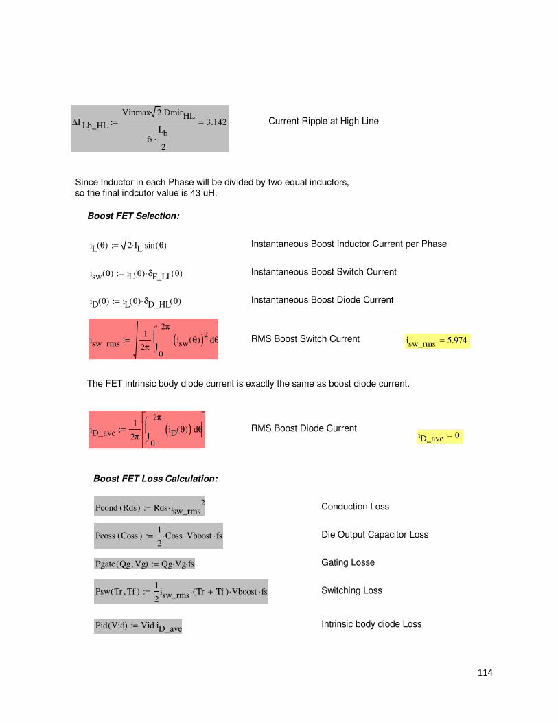
114
Current Ripple at High Line
Since Inductor in each Phase will be divided by two equal inductors, so the final indcutor value is 43 uH.
Boost FET Selection:
Instantaneous Boost Inductor Current per Phase
Instantaneous Boost Switch Current
Instantaneous Boost Diode Current
RMS Boost Switch Current
The FET intrinsic body diode current is exactly the same as boost diode current.
RMS Boost Diode Current
Boost FET Loss Calculation:
Conduction Loss
Die Output Capacitor Loss
Gating Losse
Switching Loss
Intrinsic body diode Loss
∆I Lb_HL
Vinmax 2⋅ DminHL⋅
fsLb
2⋅
3.142=:=
iL θ( ) 2 IL⋅ sin θ( )⋅:=
isw θ( ) iL θ( ) δF_LL θ( )⋅:=
iD θ( ) iL θ( ) δD_HL θ( )⋅:=
isw_rms1
2π0
2π
θisw θ( )( )2⌠⌡
d:= isw_rms 5.974=
iD_ave1
2π0
2π
θiD θ( )( )⌠⌡
d
:=iD_ave 0=
Pcond Rds( ) Rds isw_rms2
⋅:=
Pcoss Coss( )1
2Coss⋅ Vboost⋅ fs⋅:=
Pgate Qg Vg, ( ) Qg Vg⋅ fs⋅:=
Psw Tr Tf, ( )1
2isw_rms Tr Tf+( )⋅ Vboost⋅ fs⋅:=
Pid Vid( ) Vid iD_ave⋅:=
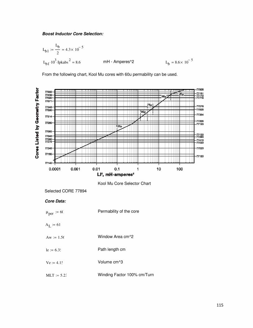
115
Boost Inductor Core Selection:
mH - Amperes^2
From the following chart, Kool Mu cores with 60u permability can be used.
Kool Mu Core Selector Chart
Selected CORE 77894
Core Data:
Permability of the core
Window Area cm^2
Path length cm
Volume cm^3
Winding Factor 100% cm/Turn
Lb1
Lb
24.3 10
5−×=:=
Lb1 103
⋅ Ipkabs2
⋅ 8.6= Lb 8.6 105−
×=
µper 60:=
AL 61:=
Aw 1.56:=
le 6.35:=
Ve 4.15:=
MLT 5.23:=
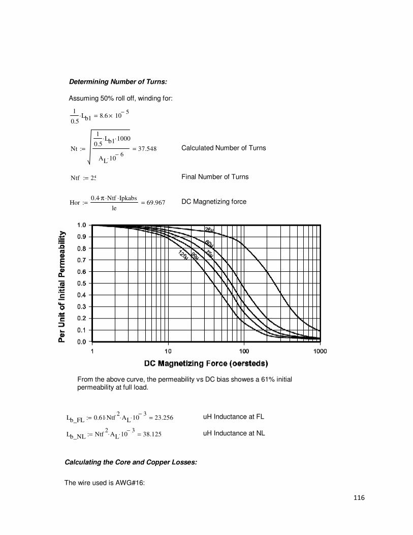
116
Determining Number of Turns:
Assuming 50% roll off, winding for:
Calculated Number of Turns
Final Number of Turns
DC Magnetizing force
From the above curve, the permeability vs DC bias showes a 61% initial permeability at full load.
uH Inductance at FL
uH Inductance at NL
Calculating the Core and Copper Losses:
The wire used is AWG#16:
1
0.5Lb1⋅ 8.6 10
5−×=
Nt
1
0.5Lb1⋅ 1000⋅
AL 106−
⋅
37.548=:=
Ntf 25:=
Hor0.4 π⋅ Ntf⋅ Ipkabs⋅
le69.967=:=
Lb_FL 0.61 Ntf2
⋅ AL⋅ 103−
⋅ 23.256=:=
Lb_NL Ntf2
AL⋅ 103−
⋅ 38.125=:=
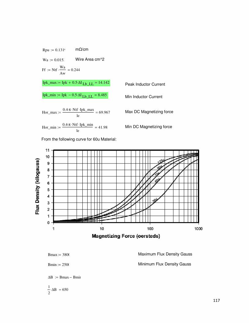
117
mΩ/cm
Wire Area cm^2
Peak Inductor Current
Min Inductor Current
Max DC Magnetizing force
Min DC Magnetizing force
From the following curve for 60u Material:
Maximum Flux Density Gauss
Minimum Flux Density Gauss
Rpu 0.1319:=
Wa 0.0152:=
Ff NtfWa
Aw⋅ 0.244=:=
Ipk_max Ipk 0.5 ∆I Lb_LL⋅+ 14.142=:=
Ipk_min Ipk 0.5 ∆I Lb_LL⋅− 8.485=:=
Hor_max0.4 π⋅ Ntf⋅ Ipk_max⋅
le69.967=:=
Hor_min0.4 π⋅ Ntf⋅ Ipk_min⋅
le41.98=:=
Bmax 3800:=
Bmin 2500:=
∆B Bmax Bmin−:=
1
2∆B⋅ 650=

118
Core losses mW/cm^3
Core losses W
Coil resistivity mΩ
DC Copper Losses W
Wire Gage factor for AWG#16
AC Resistance at Switching frequency
AC Copper Losses
Total Inductor losses per phase
PFC Bus Capacitor Selection:
Capacitance Value
Minimum Hold Up time for 50Hz
Maximum Allowable PFC Voltage Droop
PFC DC Current
Minimum Required Bus Capacitance
Pc_pu1
2
∆B
103
⋅
2fs
1000
1.46
⋅ 795.54=:=
Pc Pc_puVe
1000⋅ 3.301=:=
Rdc MLT Ntf⋅ Rpu⋅ 17.246=:=
PcuRdc
1000IL
2⋅ 1.104=:=
Kf 14.25:=
RacRdc
100Kf⋅
fs
106
⋅ 1.028=:=
Pac Rac∆I Lb_LL
2 3⋅
2
⋅ 2.742=:=
Ptot Pc Pcu+ Pac+ 7.147=:=
Tholdup1
8
1
50⋅ 2.5 10
3−×=:=
Vpfc_droop 20:=
IoPout1
Vboost9.062=:=
Cpfc2 Pout1⋅ Tholdup⋅
Vboost2
Vboost Vpfc_droop−( )2
−
:=
Cpfc 1.162 103−
×=

119
Capacitors RMS Current:
Total rms ripple current of PFC Caps
2 x Line Frequency rms ripple current
High Frequency Ripple current of PFC Caps
Part 2 - Control Component Selction
Device Parameters Definition
Refrence and Internal Bias Voltage
Current Amplifier Ox Transconductance
Voltage Amplifier O Transconductance
PWM ramp amplitude
Timing regulation Voltage at RDM
Timing regulation Voltage at RT
Timing regulation Voltage at DMAX
1 - Component Selection for RT and DMX:
Calculate RRT for target switching frequency: target
Standard Value chosen
ichf_t Io16 Vboost⋅
6 π⋅ 2⋅ Vinmin⋅ η12
⋅
1−⋅ 12.528=:=
ichf_lfIo
26.408=:=
ichf_hf Io16 Vboost⋅
6 π⋅ 2⋅ Vinmin⋅ η12
⋅
1.5−⋅ 10.765=:=
VREF 6:=
gmi 100 106−
⋅:=
gmv 70 106−
⋅:=
Vramp 4:=
VRDM 3:=
VRT 3:=
VDMAX 3:=
fsw 175:= KHz
RRT7500 10
3⋅
fsw4.286 10
4×=:=
RRT 43.2 103
⋅:=

120
Actual nominal switching frequency (KHz) will be:
Power dissipation is negligible. Select a suitable size and power rating for the resistor.
Calculate RRDM for desired maximum duty cycle:
Target
Standard Value chosen
Actual
2 - Component Selection for CDR and RDM frequency Dithering:
KHz Frequency Dithering Range
Standard Value chosen
KHz Frequency Dithering Range
pF
pF
3 - Component Selection - Vsense snd Vinac Resistor Configuration:
Choose the voltage feedback resistor divider network: VREFfb = 3
desired target
fsw750010
3⋅
RRT
:= fsw 173.611= KHz
Dmax 0.95:=
RDMX RRT 2Dmax 1−( )⋅:= RDMX 3.888 104
×=
RDMX 39.2 103
⋅:=
Dmax1
2
RDMX
RRT
1+
:= Dmax 0.954=
fdm 0.07 fsw⋅ 12.153=:=
RRDM937.510
3⋅
fdm7.714 10
4×=:=
RRDM 76.8 103
⋅:=
fdr 1:=
CRDM 66.7
RRDM
1000
fdr
⋅ 5.123 103
×=:=
CRDM 5100:=
VREFfb 3:= VOUT_AVG 400:=

121
Voltage divider resistor B
RA = R1 + R2 + R3 Voltage divier resistors A
Total power dissipation
Select Components for Vinac Divider:
Vinac sense resistors must be the same divider-ratio as that of the Vout sense resistors. Perferably, they would be the same values and ratings.
4 - Size current-sense resistor for a 3.0V dynamic range:
Choose current sense transformer turns ratio NCT:
(Use 120% of Ipk to allow for a little extra current/power to recover from large load-step or line-step changes, or line drop-outs.)
Choose a standard value:
(Power will actually be somewhat lower than this because of less than 100% duty-cycle of Ipk.)
Choose a 1/4-watt resistor.
RB 24.9 103
⋅:=
RA RB
VOUT_AVG
VREFfb
1−
⋅ 3.295 106
×=:=
R1 1.1 106
⋅:=
RA 3 R1⋅:=
PRdiv
VOUT_AVG2
RA RB+:= PRdiv 0.048=
VOUT
RA
RB
1+
VREFfb⋅:= VOUT 400.59=
NCT 100:=
Rs3 NCT⋅
Ipk 1.20⋅:=
Rs 22.097=
Rs 22.1:=
P_rsIpk
2
2Rs
NCT2
⋅:=
P_rs 0.141=

122
5 - Select components for Pulse by Pulse Current limiting:
a. Calculate the peak limit voltage: Peak current limit is a cycle-by-cycle limit which determines the absolute peak value of MOSFET drain current allowable (per phase). If this limit is exceeded, the current PWM cycle is shut down. The peak value of the inductor ripple current must be included, as well as any multipling factor used in the average current limit calculation.
b. Calculate Ipeak Resistor Divider
Limit current out of Vref to less than 0.5mA to minimize loading, since these resistors will be off of the Vref.
Select standard bottom divider-resistor value
Select standard top divider-resistor value
Resistor power dissipation is negligible; choose any suitable size and rating.
Actual peak limit voltage:
Actual peak MOSFET current per phase:
VpklmtIpk 0.5 ∆I Lb_LL⋅+( ) 1.20⋅
NCT
Rs⋅:= Vpklmt 3.75=
VREF
0.5 103−
⋅
1.2 104
×= VREF 0.5 103−
⋅( )⋅ 3 103−
×=
Vpklmt
VREF
1.2 104
×( )⋅ 7.501 103
×=
Rpklmt2 7.5 103
⋅:=
Rpklmt1VpklmtRpklmt2⋅
VREF
:=
Rpklmt1 4.688 103
×=
Rpklmt1 4.53 103
⋅:=
Vpklmt VREFRpklmt2
Rpklmt1 Rpklmt2+⋅:= Vpklmt 3.741=
IpeakVpklmt
RsNCT⋅:= Ipeak 16.926=

123
Make sure PKLMT voltage is set properly to: a) co-ordinate with low-line power limit, b) account for PKLMT detection propagation delay, and c) allow for additional saturation swing at extra power levels.
6 - Current Synthesizer:
The Resistor-Divider Atenuation at the Vsense and Vinac
Boost Inductor uH
KΩ Selected Standard Resistor
7 - Multiplier Set up:
Output of Voltage-error Amplifier
Min Voltage Feed Forward Factor
Lowest Max Power Limit
Accounting for 2-V bridge drop
Choose standard value:
kR
RB
RA RB+:=
LB Lb 106
⋅ 86=:=
RSYN
10 NCT⋅ LB⋅ kR⋅
Rs29.143=:=
RSYN 30.1:=
VAOmax 5:=
kVFF 0.398:=
VVINAC 0.76:=
Imo_max
17 106−
⋅ VVINAC⋅ VAOmax 1−( )⋅
kVFF
:= Imo_max 1.298 104−
×=
VINAC 73:=
Iin_pk 2Pout1 1.1⋅
η1⋅
1
VINAC
⋅:= Iin_pk 78.421=
RIMOIpkabs Rs⋅
NCT Imo_max⋅:= RIMO 2.407 10
4×=
RIMO 24.9 103
⋅:=

124
8 - Current Loop Compensation Design:
For I-loop compensation calculations, set Lboost to mid-way between max and min swing values (50uH to ~100uH).
select target cut off frequency
Current-Loop Plant Transfer Function:
Initial I-loop compensation target values:
i 1 2000..:=
fi
100
i 200−( )
500:=
wi
fi
:=
si
2 π⋅ j⋅ wi
⋅:=
Vout 400:=
Lboost 86 106−
⋅:=
fcxo 16 103
⋅:=
Gipi
VoutRs
NCT
⋅
si
Lboost⋅ Vramp⋅:=
dBGipi
20 log Gipi( )⋅:= φGip
iatan2 Re Gip
i( ) Im Gipi( ), ( )
180
π⋅:=
Rz1
gmi
VoutRs
NCT
⋅
2 π⋅ fcxo⋅ Lboost⋅ Vramp⋅
3.912 103
×=:=
Cz1
2 π⋅fcxo
3
⋅ Rz⋅
7.628 109−
×=:=
Cp1
2 π⋅ 2 fcxo⋅( )⋅ Rz⋅1.271 10
9−×=:=
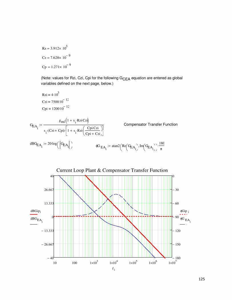
125
(Note: values for Rzi, Czi, Cpi for the following GCEA equation are entered as global
variables defined on the next page, below.)
Compensator Transfer Function
Rz 3.912 103
×=
Cz 7.628 109−
×=
Cp 1.271 109−
×=
Rzi 4 103
⋅≡
Czi 75001012−
⋅≡
Cpi 12001012−
⋅≡
GEAi
gmi 1 si
Rzi⋅ Czi⋅+( )⋅
si
Czi Cpi+( )⋅ 1 si
Rzi⋅Cpi Czi⋅
Cpi Czi+
⋅+
⋅
:=
dBGEAi
20 log GEAi
⋅:=φG EA
iatan2 Re GEA
i
Im GEAi
,
180
π⋅:=
10 100 1 103
× 1 104
× 1 105
× 1 106
× 1 107
×
40−
26.667−
13.333−
0
13.333
26.667
40
180−
150−
120−
90−
60−
30−
0
Current Loop Plant & Compensator Transfer Function
dBGipi
dBGEAi
φGip i
φG EAi
f i
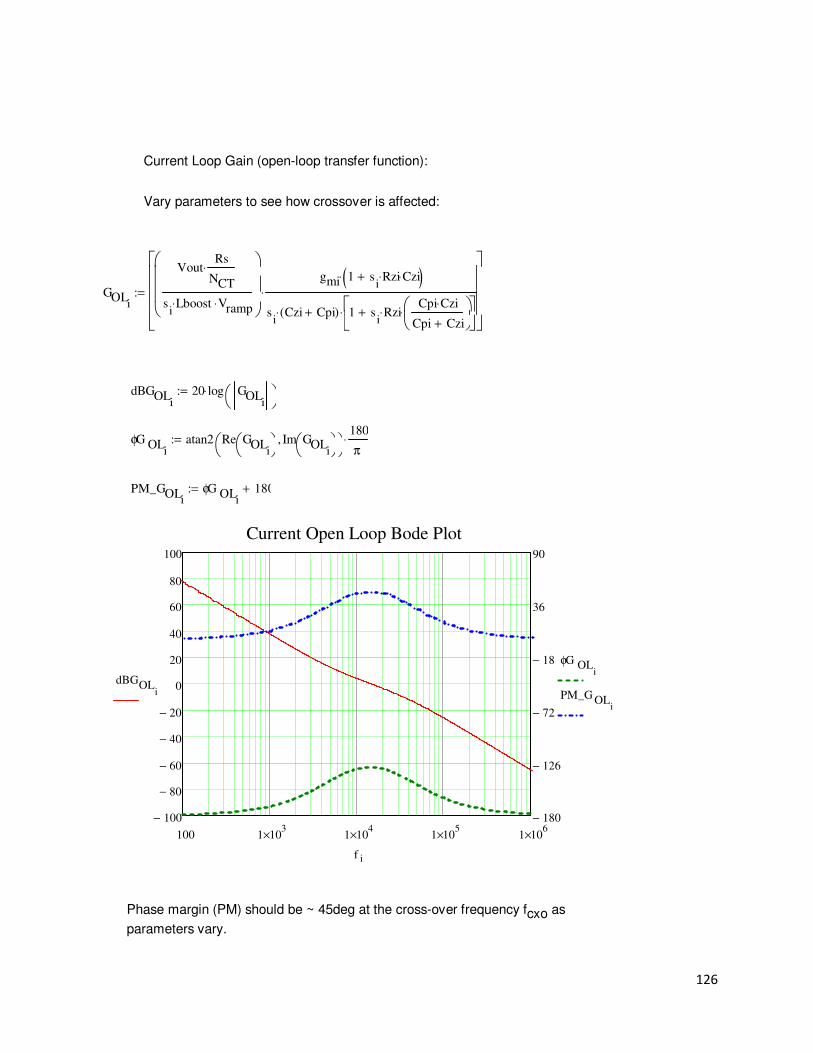
126
Current Loop Gain (open-loop transfer function):
Vary parameters to see how crossover is affected:
Phase margin (PM) should be ~ 45deg at the cross-over frequency fcxo as
parameters vary.
GOLi
VoutRs
NCT
⋅
si
Lboost⋅ Vramp⋅
gmi 1 si
Rzi⋅ Czi⋅+( )⋅
si
Czi Cpi+( )⋅ 1 si
Rzi⋅Cpi Czi⋅
Cpi Czi+
⋅+
⋅
⋅
:=
dBGOLi
20 log GOLi
⋅:=
φG OLi
atan2 Re GOLi
Im GOLi
,
180
π⋅:=
PM_GOLi
φG OLi
180+:=
100 1 103
× 1 104
× 1 105
× 1 106
×
100−
80−
60−
40−
20−
0
20
40
60
80
100
180−
126−
72−
18−
36
90
Current Open Loop Bode Plot
dBGOLi
φG OLi
PM_G OLi
f i

127
9 - Voltage Loop Compensation Design:
a. Evaluate Modulator and Power Stage Gain
PFC Voltage-Loop Boost Plant Transfer Function:
This approximation is valid for frequencies well below the LC resonance frequency. The low voltage-loop cross-over freq helps ensure this condition is true.
PinPout1
η13.68 10
3×=:=
∆Vea 3.3:=
Cpfc 1200106−
⋅:=
Gvpi
Pin1
∆Vea Cpfc⋅ Vout⋅ si
⋅:=
dBGvpi
20 log Gvpi
⋅:= φG vpi
atan2 Re Gvpi
Im Gvpi
,
180
π⋅:=
0.1 1 10 100 1 103
×
100−
80−
60−
40−
20−
0
20
40
60
80
100
135−
117−
99−
81−
63−
45−
Voltage Loop Plant Transfer Function
dBGvpi
φG vpi
f i

128
b. Evaluate Compensation Scheme
H1 is "gain" of the VSENSE resistor-divider network.
From above, Bulk Capacitor zero-peak ripple voltage:
for
Voltage error amplifier gain is adjusted with compensation components to attenuate the twice-line frequency ripple (vClf) on the output capacitor to obtain a desired reduction of 3rd harmonic THD.
Cpv sets the reduction level, Rzv sets the phase margin to 45degrees at fvxo, and Czv sets the beginning of phase boost.
Vary standard values and parameters to check fvxo and Phase Margin (PM) under different conditions. Typically: 0.00 < kPin < 1.0, 0.8 < kCout < 1.2, 0.8 < kgmv < 1.2
VREFfb 3:= Vout 400=
H1
VREFfb
Vout:= H1 7.5 10
3−×=
1
H1
133.333=
vClfPin1
2 π⋅ 100⋅ Cpfc Vout⋅:= vClf 12.202= Cpfc 1.2 10
3−×=
%k3rd 1.5:= f2LF 100:= gmv 70 106−
⋅:=
Zov f2LF( )%k3rd 66⋅ 10
3−× Vout⋅ 2⋅ π f2LF Cpfc⋅
gmv H1⋅ Pin1⋅:=
Cpv1
2π f2LF Zov f2LF( )⋅:= Cpv 1.03 10
7−×=
fvxo
gmv H1⋅ Pin1⋅
∆Vea Vout⋅ 2π( )2
⋅ Cpv⋅ Cpfc⋅
:= fvxo 17.321=
Rzv1
2π fvxo Cpv⋅:=
Rzv 8.923 104
×=
Czv10
2π fvxo Rzv⋅:= Czv 1.03 10
6−×=

129
Calculated values:
Select standard values:
Cpv 1.03 107−
×= Rzv 8.923 104
×= Czv 1.03 106−
×=
Cpv 0.05 106−
⋅:= Rzv 91 103
⋅:= Czv 0.5 106−
⋅:=
GVLi
Pin1
∆Vea Cpfc⋅ Vout⋅ si
⋅H1⋅
01.0 gmv⋅( ) si
Rzv⋅ Czv⋅ 1+( )⋅
si
Czv Cpv+( )⋅
si
Rzv⋅ Czv⋅ Cpv⋅
Czv Cpv+1+
⋅
⋅:=
dBGVLi
20 log GVLi
⋅:=φG VL
iatan2 Re GVL
i
Im GVLi
,
180
π⋅:=
PM_GVLi
φG VLi
180+:=
0.1 1 10 100 1 103
×
100−
80−
60−
40−
20−
0
20
40
60
80
100
180−
126−
72−
18−
36
90
Voltage Open Loop Bode Plot
dBGVLi
φG VLi
PM_G VLi
f i
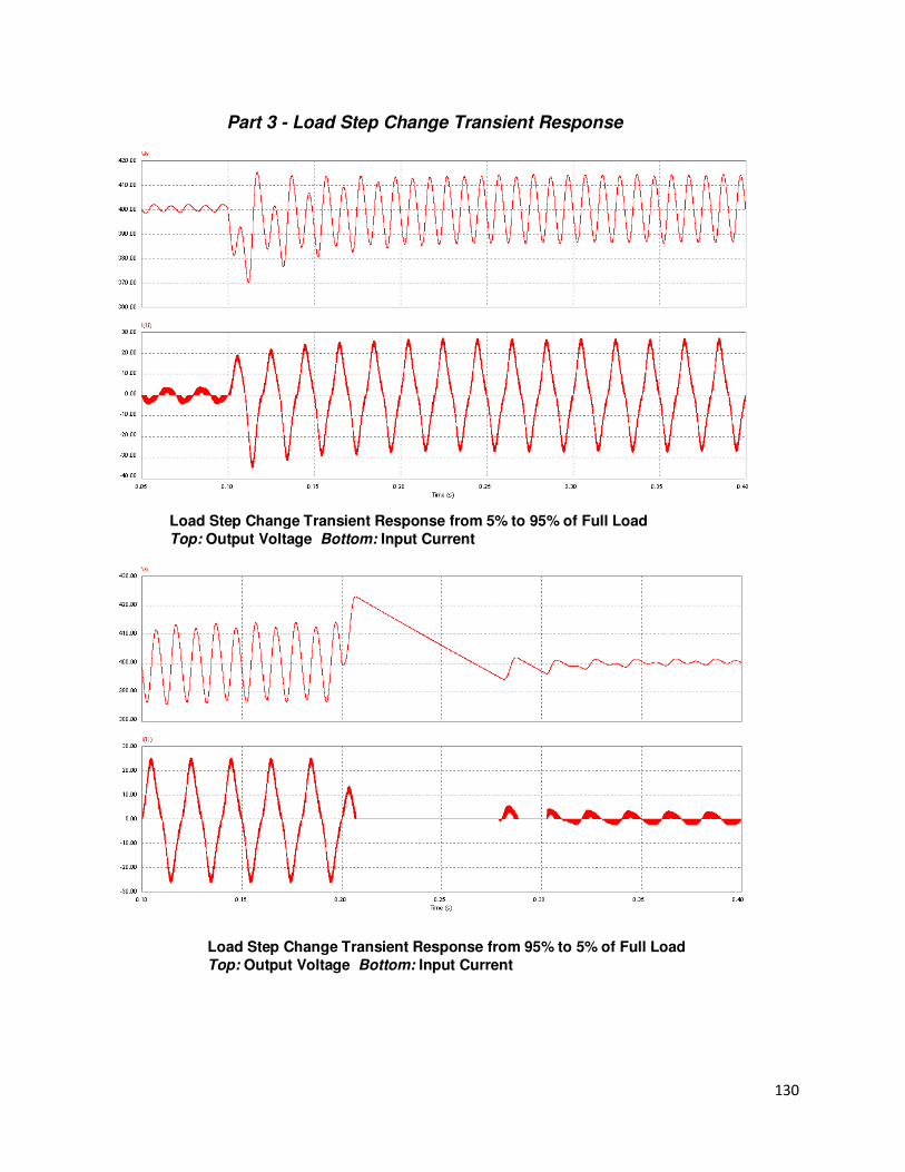
130
Part 3 - Load Step Change Transient Response
Load Step Change Transient Response from 5% to 95% of Full Load
Top: Output Voltage Bottom: Input Current
Load Step Change Transient Response from 95% to 5% of Full Load
Top: Output Voltage Bottom: Input Current