Real-Time Ozone Detection Based on a Microfabricated Quartz Crystal Tuning Fork Sensor
Upload
khangminh22Category
view
3download
0
An Investigation into the Phase Noise of
Quartz Crystal Oscillators
Brendon Bentley
Thesis presented in partial fulfilment of the requirements for the degree of
Master of Science in Engineering at the Stellenbosch University.
Supervisor: Prof. J.B. De Swardt
March 2007

Declaration
I, the undersigned, hereby declare that the work contained in this thesis is my own original
work and that I have not previously in its entirety or in part submitted it at any university
for a degree.
------------------------------------
B. F. Bentley
------------------------------------
Date
ii

Abstract
Keywords – phase noise, quartz crystal oscillator(s), frequency stability
As secondary objective an introduction to the quantification, theory and measurement of
phase noise is presented to make this field of study more accessible for the novice to the
field. Available phase noise theory is evaluated at the hand of its application to the design
of a low phase noise quartz crystal oscillator.
A low phase noise crystal oscillator was designed by application of the presented theory.
This oscillator was constructed and measured yielding phase noise low enough to compare
favourably with commercially available ultra-low phase noise crystal oscillators. Within
the sensitivity of the phase noise measurement equipment good agreement between the
theoretically predicted and the measured phase noise was achieved.
iii

Opsomming
Sleutelwoorde – faseruis, kwarts-kristal ossillator(s), frekwensie stabiliteit
‘n Doelstelling was om die studieveld van faseruis meer toeganklik te maak vir nuwelinge
tot hierdie gebied. Daar is na hierdie doelstelling gewerk deur ‘n inleidende aanbieding tot
die uitdrukking, teorie en meting van faseruis. Hierdie teorie is verder ondersoek om die
toepassing daarvan op die ontwerp van ‘n lae faseruis kristalossillator te vergemaklik.
Deur die toepassing van faseruis teorie is ‘n lae faseruis kristalossillator ontwerp, gebou en
gemeet. Meetresultate van hierdie ossillator toon dat dit goed vergelyk met komersieel
beskikbare ultralae faseruis ossillators. Goeie ooreenstemming tussen die teoreties
voorspelde faseruis en die faseruis soos dit gemeet was is gevind binne die sensitiwiteit van
die meettoerusting.
iv

Acknowledgements
I would like to express my sincere gratitude to everyone who contributed to this thesis.
Thanks to my lord and God, Jesus Christ, who knows my every weakness and who strengthened and encouraged me during every day’s work despite them. You are worthy, our Lord and God, to receive glory and honour and power, for you created all things, and by your will they were created and have their being*.
I would like to thank my supervisor, Prof. J.B. De Swardt, for his guidance, advice and encouragement which was indispensable during this project.
Much gratitude is also due to Armscor for financial support for this project, without which this project would not have been possible.
I also appreciate useful comments and suggestions made by Prof. P.W. van der Walt – especially during the start of this project.
I am very thankful for the daily encouragement and support that I received from Gillian de Villiers.
The technical staff at the electronics workshop of the University of Stellenbosch, especially Mr. Wessel Craukamp, is also thanked for their stellar work with the manufacture of aluminium heat tank blocks which was a critical part of the temperature controller that was constructed.
Mr. Martin Siebers from the high frequency and antenna measurement laboratory at the University of Stellenbosch is also thanked for friendly and helpful assistance during measurements.
Much thanks is also due to my friends and family who supported and encouraged me over the duration of this project. Special mention can be made here of Mrs. Kotie Smuts who provided me with accommodation in Stellenbosch to complete the last part of this project.
* Revelation 4:11, The Bible (NIV)
v

Contents List of Figures .............................................................................................................................. x
List of Tables ............................................................................................................................ xiii
Definition of terms.................................................................................................................... xiv
1. Introduction.......................................................................................................................... 1
1.1. Problem Statement...........................................................................................................1
1.2. Proposed Solution............................................................................................................2
1.3. Aims & Contributions of Dissertation.............................................................................3
1.4. Overview of the Thesis ....................................................................................................3
2. Introductory phase noise theory & phase noise prediction ............................................. 5
2.1. Introduction to phase noise ..............................................................................................5
2.2. Physical causes and characterization of noise in systems ...............................................6
2.2.1. What is noise and why does it exist? ....................................................................6
2.2.2. Thermal noise........................................................................................................6
2.2.3. Shot noise..............................................................................................................9
2.2.4. Other kinds of noise ............................................................................................10
2.2.5. Characterization of phase noise ..........................................................................11
2.3. Contributing mechanisms to phase noise ......................................................................19
2.4. Generally available phase noise models ........................................................................20
vi

2.4.1. Leeson’s model ...................................................................................................21
2.4.1.1. Conclusion on Leeson’s model ................................................................. 24
2.4.2. Lee & Hajimiri’s model ......................................................................................25
2.4.2.1. Conclusion on Lee & Hajimiri’s model.................................................... 28
2.4.3. Demir, Mehrotra & Roychowdhury’s model......................................................30
2.4.3.1. Conclusion on Demir, Mehrotra & Roychowdhury’s model.................... 31
2.4.4. Conclusions and Comparisons of Phase Noise Models......................................32
2.5. Conclusion .....................................................................................................................34
3. Quartz crystal resonators: fundamental physics, modelling and quality factor...........36
3.1.1. Fundamental physics of quartz resonators..........................................................36
3.1.2. Modelling and measurement of resonators .........................................................43
3.1.3. A brief word on AT-cut and SC-cut quartz resonators .......................................50
4. The quantification and measurement of frequency stability ......................................... 52
4.1. Measurable parameters that can be related to frequency stability .................................53
4.2. Relation of measured parameters to the single sided spectral density of phase, ( )fL .55
4.3. Methods of phase noise measurement ...........................................................................58
4.3.1. Direct (spectrum analyzer) measurement ...........................................................58
4.3.2. Heterodyne (or beat frequency) measurement ....................................................60
4.3.3. Carrier removal measurement (also known as demodulation methods) .............62
4.3.3.1. Frequency demodulation (measurement with frequency discriminator e.g. delay line with mixer, cavity, bridge types, etc.) ............................... 62
vii

4.3.3.2. Phase demodulation (measurement with phase detectors)........................ 64
4.3.4. Time difference method......................................................................................66
4.3.5. Dual mixer time difference (DMTD) method.....................................................68
4.4. Comparison of measurement methods...........................................................................72
4.5. What measurement was used for this project and why?................................................74
4.6. Measurement procedure.................................................................................................75
4.6.1. Measurement on moderate phase noise oscillators .............................................77
4.6.2. Measurement on low phase noise oscillators......................................................80
4.7. Conclusion .....................................................................................................................82
5. Design of a low phase noise crystal oscillator.................................................................. 83
5.1. Design of a Driscoll oscillator .......................................................................................86
5.2. Phase noise prediction of a Driscoll oscillator ..............................................................92
5.3. Conclusion .....................................................................................................................96
6. Measurements and results................................................................................................. 97
6.1. Measurement of the residual system noise ....................................................................98
6.2. Measurement of the Driscoll oscillator........................................................................102
6.3. Conclusion ...................................................................................................................106
7. General conclusion........................................................................................................... 109
7.1. Conclusion ...................................................................................................................109
7.2. Recommendations........................................................................................................110
viii

Appendices.............................................................................................................................. 111
A. Detailed discussion of the phase demodulation method of measuring phase noise111
A.1 Characteristic of a double balanced mixer which is used as a phase detector....................................................................................................... 111
A.2 Measurement and calibration of the phase fluctuation, φΔ .......................114
A.3 Relationship of the phase fluctuation, φΔ , to the SSB phase noise relative to the carrier, ( )fL ........................................................................115
B. A temperature controller for quartz crystal resonators ...........................................117
C. Design and implementation of a strategy to make the high quality factor quartz crystal resonators frequency selectable...................................................................120
References............................................................................................................................... 123
ix

Figures Figure 2.1: The mechanism of thermal noise ............................................................................ 7
Figure 2.2: Equivalent noise models for a noisy resistor in terms of current noise sources, voltage noise sources and noiseless resistors.......................................................... 8
Figure 2.3: The mechanism of shot noise.................................................................................. 9
Figure 2.4: A general signal superimposed upon its theoretically desired counterpart........... 11
Figure 2.5: Time domain plot illustrating how a phase fluctuating signal loses synchronization with respect to a phase stable reference signal........................... 12
Figure 2.6: Phasor representation of a general sinusoidal signal exhibiting phase noise........ 14
Figure 2.7: Frequency representation of phase noise .............................................................. 18
Figure 2.8: Leeson's model provides an asymptotic approximation over three regions of phase noise decline with frequency ...................................................................... 23
Figure 3.4: Visual representation of a quartz crystal............................................................... 37
Figure 3.5: Estimated and achieved internal friction characteristics of quartz resonators ...... 38
Figure 3.6: Orientation of a quartz crystal resonator wafer relative to the crystal axes.......... 39
Figure 3.7: Modes of vibration of quartz crystal wafers ......................................................... 40
Figure 3.8: Typical frequency-temperature characteristic curves for quartz resonators ......... 41
Figure 3.9: Circuit diagram symbol and electrical model of a quartz crystal resonator.......... 43
Figure 3.10: The reactance-frequency relationship of a quartz crystal resonator ..................... 44
Figure 3.11: Admittance measurement of resonator for model parameter extraction............... 47
Figure 3.12: Photograph of the different quartz crystal resonators that were used in oscillators for this project...................................................................................... 50
Figure 4.1: Measurement setup for measuring phase noise by means of the direct (or spectrum analyzer) measurement method............................................................. 58
Figure 4.2: Measurement setup for measuring phase noise by means of the heterodyne (or beat frequency) measurement method .................................................................. 60
x

Figure 4.3: Measurement setup for measuring phase noise by means of the frequency demodulation (or frequency discriminator) measurement method....................... 62
Figure 4.4: Measurement method for measuring phase noise by means of the phase demodulation (or phase detector) measurement method ...................................... 64
Figure 4.5: Measurement of phase noise by means of the time difference measurement method................................................................................................................... 66
Figure 4.6: Measurement of phase noise by means of the dual mixer time difference method................................................................................................................... 68
Figure 4.7: Comparison of best achievable phase noise sensitivities of three popular phase noise measurement methods for a 10 GHz oscillator ........................................... 72
Figure 4.8: Photograph of the Aeroflex PN900B Phase Noise Measurement System............ 74
Figure 4.9: Moderate phase noise oscillator measurement setup ............................................ 77
Figure 4.10: Phase noise of the PN9100 RF Synthesizer reference oscillator at 10 MHz ........ 78
Figure 4.11: Low phase noise oscillator measurement setup .................................................... 80
Figure 5.1: Driscoll oscillator circuit where non-linear limiting is restricted to a single active element – i.e. a Schottky barrier diode, D1 ................................................ 86
Figure 5.2: An equivalent circuit from the perspective of the transformer T1 where the sub-circuits connected to the primary and secondary windings have been reduced to equivalent impedances ........................................................................ 89
Figure 5.3: Series-parallel equivalent circuits used for impedance matching. It is important to note that this equivalence is dependent upon the presence of an inductor further on between ports a and b (which is not shown in this diagram). 90
Figure 5.4: Operation of a low-phase noise Schottky diode sub-circuit to which non-linear operation is limited in the Driscoll oscillator........................................................ 90
Figure 5.5: Determination of the oscillator noise figure, F, of Driscoll’s oscillator for phase noise prediction through Leeson’s phase noise model ............................... 93
Figure 5.6: Predicted phase noise for the Driscoll oscillator with circuit diagram of figure 5.1.......................................................................................................................... 96
Figure 6.1: A photograph of the part of the high frequency and antenna measurement laboratory at the University of Stellenbosch where the phase noise measurements were taken ..................................................................................... 98
Figure 6.2: Transmission line and lumped element circuit diagrams for the quadrature hybrid. ................................................................................................................... 99
xi

Figure 6.3: A photograph of the lumped element quadrature hybrid that was constructed with the element values of equations 6.1. ........................................................... 100
Figure 6.4: Scattering parameter measurement results for the designed quadrature hybrid. 101
Figure 6.5: Measurement setup for measurement of the residual phase noise of the Aeroflex PN9000B phase noise measurement.................................................... 102
Figure 6.6: Measured phase noise, residual system noise and predicted phase noise for the Driscoll oscillator that was designed and constructed. ....................................... 103
Figure 6.7: A photograph of the Driscoll oscillator that was built and measured................. 104
Figure 6.8: Output signal of Driscoll oscillator as affected by 50 mV (peak-to-peak) power supply noise at 10 kHz. ............................................................................ 105
Figure 6.9: The affect of perturbation power (at 10 kHz superimposed on DC power supply) on the phase noise sidebands.. ............................................................... 106
Figure 6.10: A comparison of the Driscoll oscillator that was designed for this project with a commercial ultra-low phase noise oscillator by Wenzel Associates, Inc. ....... 108
Figure A.1: Block diagram of the phase demodulation method of measuring phase noise ... 111
Figure A.2: The characteristic curve of a double balanced mixer which is used as a phase detector................................................................................................................ 112
Figure B.1: Circuit diagram of the temperature controller that was designed ....................... 118
Figure B.2: Photograph of temperature controller that was designed to establish long term frequency stabilisation of the quartz crystal resonators...................................... 119
Figure C.1: Circuit representation of how the crystal resonator was made frequency selectable............................................................................................................. 120
Figure C.2: Frequency selectable circuit to overcome the problems that were highlighted previously............................................................................................................ 121
xii

Tables
Table 2.1: Comparative summation of typical LTI, LTV and NLTV phase noise models ... 32
Table 4.1: Comparison of six methods of frequency instability measurement...................... 73
Table A.1: Error function for the phase demodulation measurement method...................... 113
xiii

Definition of terms
AM, amplitude modulation
anisotropic, the characteristic that the physical properties of a crystal differ significantly with the direction of the crystallographic axes
BJT, bipolar junction transistor
carrier or carrier frequency, fundamental frequency of oscillation in the oscillator
close-in phase noise, phase noise very close to the carrier frequency
cyclostationary, random behaviour that displays a statistical cyclic recurrence (usually, but not necessarily, with respect to time)
dB, decibel
dBc, decibel measured relative to the signal level of the carrier
DC, direct current, often used to refer to zero frequency
DDS, direct digital synthesizer
enantiomorphic, the property that two forms (right-handed form and left-handed form) of the same crystal exist in nature which cannot be made equivalent by simple rotation
FM, frequency modulation
ISF, impulse sensitivity function
LO, local oscillator
LTI, linear time-invariant
LTV, linear time-variant
NLTV, non-linear time-variant
OCXO, oven controlled crystal oscillator
piezo-electric effect, the two way mechanical-electrical relationship observed in some kinds of crystals
PLL, phase locked loop
xiv

PM, phase modulation
power spectral density, a power spectrum that has been normalized such that the area below the graph is unity
power spectrum, (also RF spectrum) graph of rms power (often expressed in dBm) vs. frequency, i.e. what a spectrum analyser measures
ppm, parts per million
PSU(s), power supply unit(s)
Q, quality factor
RF, radio frequency
RF spectrum, see power spectrum
rms, root-mean-square
RO, reference oscillator
SC-cut, stress-compensated quartz crystal resonator
SSB, single sideband
SUT, source under test (the oscillator that is being measured)
TCXO, temperature compensated crystal oscillator
TO, turnover temperature is inflection point in the frequency-temperature characteristic of quartz crystal resonators
time interval counter, a device which measures the time difference between the positive zero crossings of two sinusoidal time signals
USD, The currency unit (dollar) of the United Stated of America
VCO, voltage controlled oscillator
xv

Chapter 1
Introduction
In a day and age where an ever increasing demand for bandwidth is the driving force behind
wireless communication development it is the short term frequency stability of the oscillators
involved that limits the practically achievable bandwidth or channel density [1], [2]. The short
term frequency stability of oscillators is most often quantified as phase noise which also
becomes a critical consideration for oscillators involved in radar and satellite positioning
systems [2], [3], [4].
The importance of phase noise consideration in oscillators may be briefly highlighted by the
example of a radio transceiver system. Geographically close to a transmitter the phase noise of
the modulated oscillator may overwhelm adjacent channels while in the case of a receiver
system phase noise in the local oscillator (LO) may cause adjacent channels to be down-
converted into the IF-band thereby corrupting the modulated signal [5].
Phase noise of oscillators became the subject of much research since World War II when it was
first identified as a limiting factor in moving target identification (MTI) systems [3]. This has
led to the development of phase noise theories that can predict the phase noise of signal sources
with increasing accuracy as the complexity of these models increase.
1.1. Problem Statement
Quartz crystal oscillators are widely used because of their well known low phase noise and the
low cost involved. Due to physical restrictions on the dimensions of quartz crystal resonators
the upper frequency limit of these resonators is around 300 MHz. Stable frequency sources are
often designed at higher frequencies by employing a crystal oscillator as a reference source.
As the frequency stability of such a stable frequency source is directly dependent on the
1

CHAPTER 1 – INTRODUCTION
frequency stability of the reference crystal oscillator as the logarithm of the frequency ratio it is
imperative that the reference crystal oscillator display low phase noise. The problem which is
considered in this thesis is that of designing such a reference oscillator to yield ultra-low phase
noise.
Furthermore, ambiguities between different phase noise theories do arise which make it
difficult for the oscillator designer to find reliable guidance when designing oscillators for low
phase noise.
Finally, the nature of phase noise theory led to the view of many design engineers that low
phase noise oscillator design is a daunting field of engineering which is to be avoided.
1.2. Proposed Solution
The final problem outlined above, that of the exclusivity in the field of phase noise, may be
addressed by presenting definitions of concepts, overviews of the most relevant theory and
consideration of the available measurement techniques of phase noise in an easy-to-follow,
concise fashion. This must be complete enough so that a novice to the field would be able to
study further theory with minimal need for more basic literature.
The available theory should then be evaluated from a theoretical perspective to determine its
application to the design of low phase noise crystal oscillators. Lastly the central problem that
was outlined previously may directly be addressed by the application of phase noise theory to
the design of a low phase noise crystal oscillator. This would provide direction to the crystal
oscillator designer.
2

CHAPTER 1 – INTRODUCTION
1.3. Aims & Contributions of Dissertation
This thesis assumes no prior knowledge about phase noise and commences by thorough
explanations of the concepts involved in this field. This aims to make phase noise theory more
accessible to outsiders to the field of phase noise in crystal oscillators. Critical reviews of the
most important developments in phase noise theory applicable to crystal oscillator design are
also presented. Because understanding of a physical concept is often improved by a proper
understanding of its quantification and measurement, much attention is invested in a clear and
concise presentation of the quantification and measurement of phase noise.
An experimental investigation applies linear time-invariant phase noise theory to the design,
construction and measurement of an ultra-low phase noise crystal oscillator. This exercise
yields a low phase noise oscillator that compares favourably with current commercial state-of-
the-art ultra-low phase noise quartz crystal oscillators. It is concluded that linear time-invariant
phase noise theory provides reliable design techniques to the designers of low phase noise
quartz crystal oscillators.
1.4. Overview of the Thesis
Chapter 2 provides an introduction to those unfamiliar with phase noise. Section 2.2 considers
the source and characterisation of noise in electrical systems in general before presenting a
fundamental introduction to what phase noise is. Mechanisms by which the noise present in an
oscillator system would affect the phase noise is considered in section 2.3. This is followed in
sections 2.4-2.5 by a critical overview of the most important theoretical developments in the
phase noise field.
Consistent with the assumption that the reader is unfamiliar with phase noise in crystal
oscillators, chapter 3 provides the reader with a comprehensive overview of quartz crystal
resonators.
3

CHAPTER 1 – INTRODUCTION
Chapter 4 starts by explaining in section 4.1 which measurable parameters can be related to
frequency stability while section 4.2 shows how these measurable parameters may be
manipulated to yield the single sided spectral density of phase (also single sideband phase
noise relative to the carrier), . The remainder of the chapter is devoted to the explanation
of phase noise measurement methods with a detailed look at the measurement method that was
used for this project – the phase demodulation method.
( )fL
Phase noise theory was evaluated by an experimental investigation. In the first step of this
exercise chapter 5 presents the design of a low phase noise crystal oscillator by application of
linear time-invariant phase noise theory. The phase noise expectations arising from this design
were so low that phase noise measurement equipment available to the author was unable to
completely characterise the oscillator.
Chapter 6 presents the phase noise measurement of the crystal oscillator that was designed in
chapter 5. The phase noise measurement made on this oscillator shows that it compares
favourably to state-of-the-art commercial ultra-low phase noise oscillators. The design and
construction of a lumped element quadrature hybrid allows for a measurement of the residual
system noise of the phase noise measurement system. This in turn shows that the phase noise
measurement on the designed oscillator is not a true reflection of its phase noise as the phase
noise of the measurement system overshadows that of the oscillator.
Conclusions and recommendations follow in the final chapter, chapter 7.
4

Chapter 2
Introductory phase noise theory & phase noise prediction
2.1. Introduction to phase noise
In the sphere of radio frequency (RF) communication oscillators provide the reference signals
on which information is modulated in transmitters and from which it is demodulated again in
receivers. For the simplest consideration of transmitter or receiver systems it is usually
assumed that such oscillators are ideal in the sense that a single frequency tone (with perhaps
higher harmonics of this tone) is generated. When this assumption is challenged it means that
adjacent channels are disturbed by a receiver system, it limits the adjacent channel rejection in
receiver systems, it limits the bandwidth of digital communication systems and causes bit-
error-rates, it causes false target identification in radar systems and limits the accuracy with
which position may be determined by satellite navigation systems.
Noise, which is present in all electrical systems, perturbs both the amplitude and the frequency
of oscillators. The effect of frequency perturbations in oscillators is observed as power
dispersion in the RF spectrum around the fundamental (and higher modes) frequency of
oscillation. Physically this means that the oscillatory signal is changing its frequency with the
passage of time. This non-ideal effect may be quantified as phase noise.
As the phase noise of an oscillator is so crucial to the practically achievable limits of systems,
it has been widely studied and researched. Despite all this effort on obtaining insight in the
field, the study of phase noise is far from complete. Many phase noise models predict the
phase noise through simulation or rely partially on computer simulation. Often this brings little
insight to the designer who wants to design an oscillator circuit with low phase noise.
Alternative techniques often have to be investigated to obtain insightful results.
5

CHAPTER 2 – INTRODUCTORY PHASE NOISE THEORY & PHASE NOISE PREDICTION
2.2. Physical causes and characterization of noise in systems
2.2.1.What is noise and why does it exist?
The IEEE defines electrical noise as:
Unwanted electrical signals that produce undesirable effects in circuits of control systems in
which they occur. [29]
Another IEEE definition of noise as applied to analog computers presents noise as:
Unwanted disturbances superimposed upon a useful signal, which tend to obscure its
information content. Random noise is part of the noise that is unpredictable, except in a
statistical sense. [29]
This latter definition of noise points out the random nature of this phenomenon which is
inseparable of the nature of noise. Different physical processes contribute to these random
disturbances that are observed in electrical signals and it is on the criteria of these physical
processes that noise is characterised.
2.2.2.Thermal noise
Thermal noise, also called Johnson noise (after it was observed by J. B. Johnson of Bell
Telephone Laboratories in 1927) or Nyquist noise (after it was theoretically analysed by H.
Nyquist in 1928) is the result of the inherent kinetic energy associated with particles (of all
matter) in general, and primary charge carriers in specific, at temperatures above absolute zero
(that is 0 kelvin). Each of these primary charge carriers has a discrete charge associated with it
while the macroscopic effect of the random motion of these carriers is observed as small surges
of instantaneous current that are similarly random in nature. Thermal noise covers the entire
6
CHAPTER 2 – INTRODUCTORY PHASE NOISE THEORY & PHASE NOISE PREDICTION
frequency band equally and in analogy to white light it is sometimes described as ‘white noise’
[8], [9].
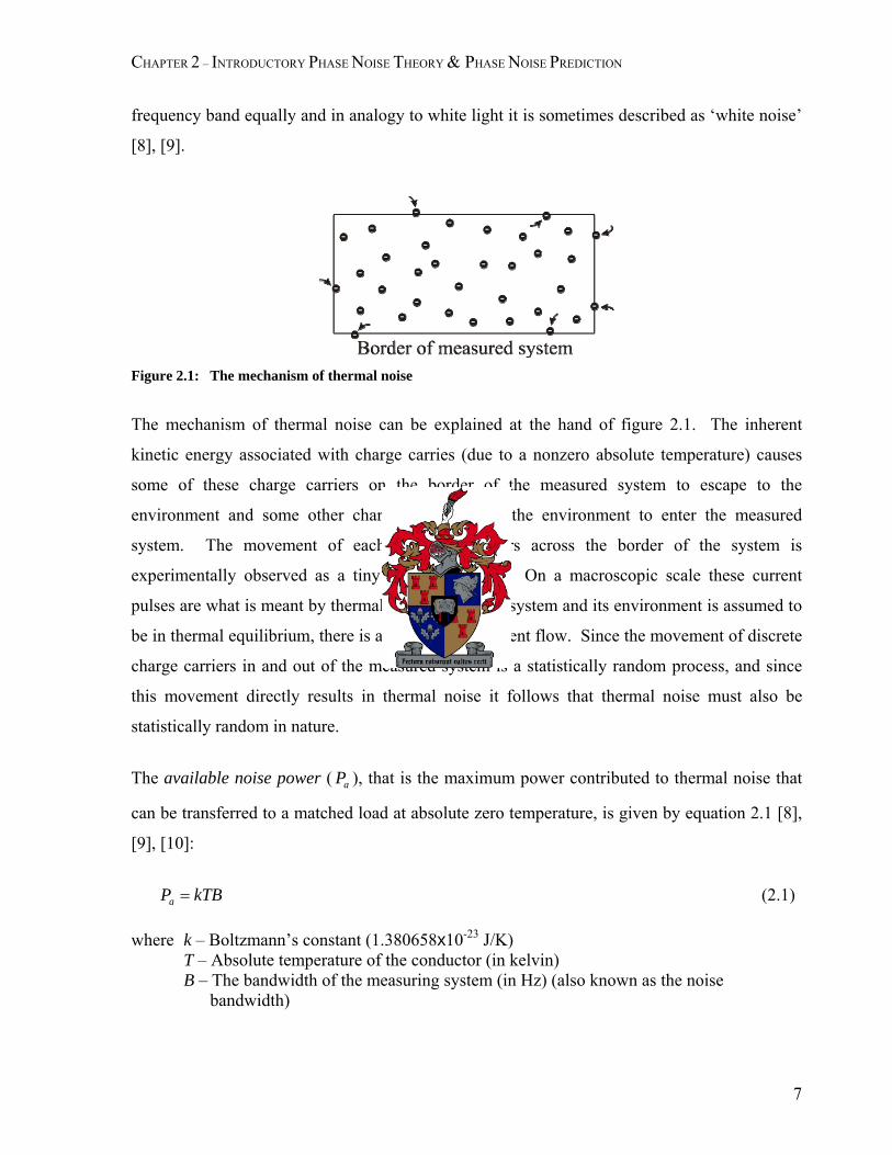
Figure 2.1: The mechanism of thermal noise
The mechanism of thermal noise can be explained at the hand of figure 2.1. The inherent
kinetic energy associated with charge carries (due to a nonzero absolute temperature) causes
some of these charge carriers on the border of the measured system to escape to the
environment and some other charge carriers from the environment to enter the measured
system. The movement of each of these carriers across the border of the system is
experimentally observed as a tiny pulse of current. On a macroscopic scale these current
pulses are what is meant by thermal noise. Since the system and its environment is assumed to
be in thermal equilibrium, there is a zero average current flow. Since the movement of discrete
charge carriers in and out of the measured system is a statistically random process, and since
this movement directly results in thermal noise it follows that thermal noise must also be
statistically random in nature.
The available noise power ( ), that is the maximum power contributed to thermal noise that
can be transferred to a matched load at absolute zero temperature, is given by equation 2.1 [8],
[9], [10]:
aP
kTBPa = (2.1)
where k – Boltzmann’s constant (1.380658x10⁻²³ J/K) T – Absolute temperature of the conductor (in kelvin) B – The bandwidth of the measuring system (in Hz) (also known as the noise bandwidth)
7
CHAPTER 2 – INTRODUCTORY PHASE NOISE THEORY & PHASE NOISE PREDICTION
From equation 2.1 it can be concluded that thermal noise alone sets a limit on the noise floor
for a particular measurement setup across any frequency range [8], [9].
Thermal noise can be modelled as a randomly fluctuating potential difference with RMS
voltage ( ) over a resistance (R) as presented in equations 2 and 3 below [8], [9]: tE
kTBR
EP ta ==
4
2
(2.2)
so that can be solved for: tE
⎪⎭
⎪⎬⎫
=
==
kTRBE
kTRBeE
t
tt
4
422 (2.3)
where 2
te – Mean square value of thermal noise
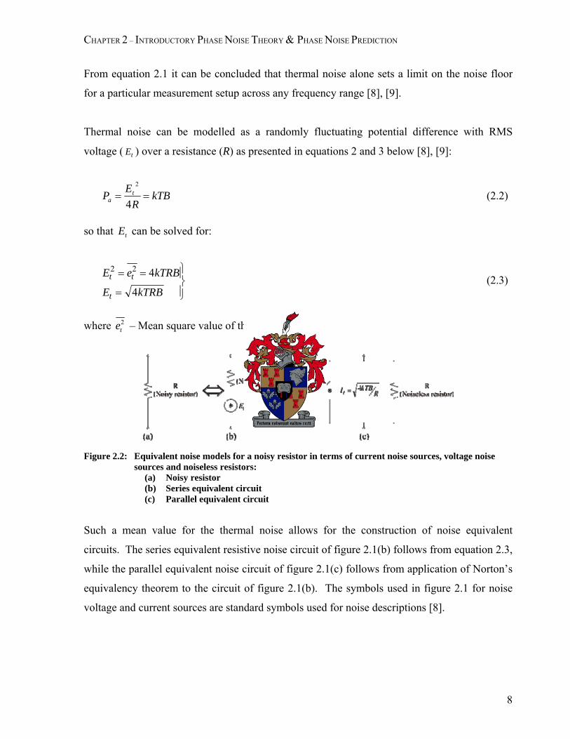
Figure 2.2: Equivalent noise models for a noisy resistor in terms of current noise sources, voltage noise
sources and noiseless resistors: (a) Noisy resistor (b) Series equivalent circuit (c) Parallel equivalent circuit
Such a mean value for the thermal noise allows for the construction of noise equivalent
circuits. The series equivalent resistive noise circuit of figure 2.1(b) follows from equation 2.3,
while the parallel equivalent noise circuit of figure 2.1(c) follows from application of Norton’s
equivalency theorem to the circuit of figure 2.1(b). The symbols used in figure 2.1 for noise
voltage and current sources are standard symbols used for noise descriptions [8].
8

CHAPTER 2 – INTRODUCTORY PHASE NOISE THEORY & PHASE NOISE PREDICTION
Noise signals and add according to equation 2.4 [8]. Signals that show no relationship
between their instantaneous values (such signals are usually produced independently) are
defined to be uncorrelated. Oppositely, signals of which the shapes are identical (while exactly
in phase or exactly out of phase, but with no regard of amplitude) are defined to be 100%
correlated. Partially correlated signals may be characterised by a correlation coefficient, C,
where . If the signals are 100% correlated and exactly in phase, if
1E 2E
11 <<− C 1=C 1−=C the
signals are 100% correlated and exactly out of phase. Finally, if , the signals are
uncorrelated and the last term in equation 2.4 may be neglected.
0=C
0=C is often assumed and
may result in a maximal error of 30% if the signals were in fact fully correlated [8].
21
22
21
2 2 ECEEEEequ ++= (2.4)
2.2.3.Shot noise
In contrast to thermal noise resulting from kinetic energy of discrete charge carriers associated
with an above absolute zero temperature, shot noise is the result of the motion of discrete
charge carriers over a potential barrier. Because these are discrete charge carriers, the resulting
current is the sum of small randomly spaced instantaneous current pulses. The time average of
this current is known as the direct current (IDC).
Figure 2.3: The mechanism of shot noise
The mechanism of shot noise can be explained at the hand of figure 2.3. A potential barrier
prompts the movement of discrete charge carriers in a set direction. The time average of the
arrival of discrete charge carriers at the one end determines the direct current. The discrete
nature in which the instantaneous current pulses are observed (due to the arrival of discrete
charge carriers at the one side and the departure of discrete charge carriers at the opposite side)
9

CHAPTER 2 – INTRODUCTORY PHASE NOISE THEORY & PHASE NOISE PREDICTION
results in shot noise. Since the time of arrival/departure of discrete charge carriers at the ends
of the measured system is a statistically random process, and since this movement directly
results in shot noise it follows that shot noise must also be statistically random in nature. An
expression for the shot noise current is available [8], [9]:
BqII DCsh 2= (2.5)
where q – electronic charge quantum ( C) 191059.1 −× IDC – direct current (in A) B – The bandwidth of the measuring system (in Hz) (also known as the noise bandwidth) Taking note of the fact that the shot noise current is dependent on the noise bandwidth rather
than on the frequency reveals that shot noise can also be described as white noise. Although
the phenomenon of shot noise is widely observed, it is most prevalent in biased semiconductor
junctions for which more specific noise expressions can be derived with the aid of equation 2.5.
Such expressions yield equivalent noise circuits similar to those in figure 2.2.
2.2.4.Other kinds of noise
Thermal noise and shot noise are sometimes referred to as ultimate noise because these kinds
of noise place a limit on the lowest achievable noise in a system. Their origins are well
understood from a material physics point of view and a quantitative theory explains their
behaviour. In contrast to this, other kinds of noise that are not well described mathematically
and depend to a large extent to the quality of the components in the concerned system, like
flicker noise and popcorn noise, are grouped together with the term excess noise [9].
Not all noise can be described as white noise. Low frequency noise that has been observed to
have a 1/f frequency dependency is referred to as pink noise, while a 1/f2 dependency is called
red noise. This 1/f-noise is encountered in even the simplest phase noise models and is further
studied in equation 2.16. Although the properties of such noise have been well documented, its
physical origins are doubted and avoided by literature.
10
CHAPTER 2 – INTRODUCTORY PHASE NOISE THEORY & PHASE NOISE PREDICTION
2.2.5.Characterization of phase noise
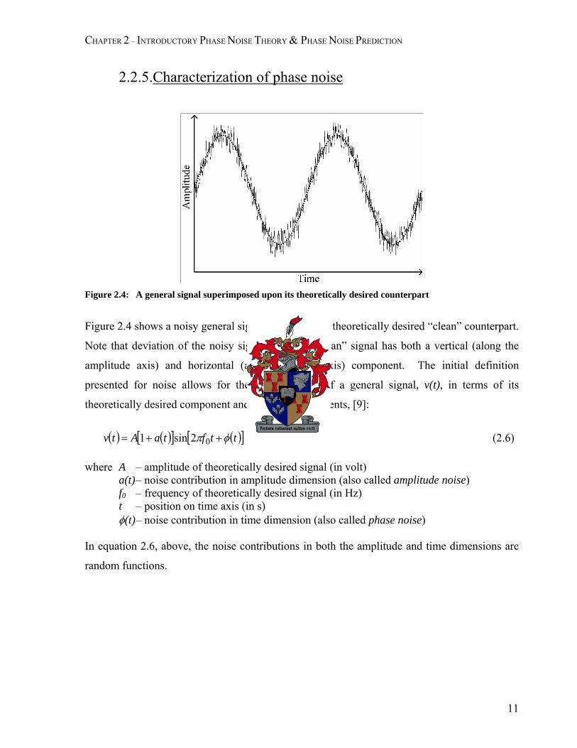
Figure 2.4: A general signal superimposed upon its theoretically desired counterpart
Figure 2.4 shows a noisy general signal along with its theoretically desired “clean” counterpart.
Note that deviation of the noisy signal from the “clean” signal has both a vertical (along the
amplitude axis) and horizontal (along the time axis) component. The initial definition
presented for noise allows for the representation of a general signal, v(t), in terms of its
theoretically desired component and its noise components, [9]:
( ) ( )[ ] ( )[ ttftaAtv ]φπ ++= 02sin1 (2.6)
where A – amplitude of theoretically desired signal (in volt) a(t) – noise contribution in amplitude dimension (also called amplitude noise) f0 – frequency of theoretically desired signal (in Hz) t – position on time axis (in s) φ(t) – noise contribution in time dimension (also called phase noise)
In equation 2.6, above, the noise contributions in both the amplitude and time dimensions are
random functions.
11

CHAPTER 2 – INTRODUCTORY PHASE NOISE THEORY & PHASE NOISE PREDICTION
0 0.05 0.1 0.15 0.2 0.25 0.3 0.35 0.4 0.45 0.5
-1
-0.8
-0.6
-0.4
-0.2
0
0.2
0.4
0.6
0.8
1
Time
Sig
nal a
mpl
itude
Sinus displaying phase noiseSinus without phase noise
Figure 2.5: Time domain plot illustrating how a phase fluctuating signal loses synchronization with respect
to a phase stable reference signal
Figure 2.5 improves one’s intuition for how phase noise contributions disturb a sinusoidal
signal in the time domain. For the case where a signal without phase noise is considered, as is
the case with the dotted-line-plot in figure 2.5, the signal amplitude goes through zero on the
amplitude axis at constant time intervals. In contrast to this the amplitude of a signal exhibiting
phase noise, as is the case with the solid-line-plot in figure 2.5, goes through zero on the
amplitude axis at irregular time intervals causing a loss of synchronization between the two
signals. Similar behaviour in square wave signals often found in digital circuits is commonly
referred to as jitter [1], [11].
In order to understand the effect that amplitude noise would have on the sidebands of the
carrier (at a frequency ) in the frequency domain, consider the special case of the general
signal in equation 2.6 where the phase noise contribution term is zero, , the amplitude
of the theoretically desired signal is unity,
0f
( ) 0=tφ
1=A , and the signal is amplitude modulated by a
pure cosine signal (at frequency ) with modulation index, f α :
12

CHAPTER 2 – INTRODUCTORY PHASE NOISE THEORY & PHASE NOISE PREDICTION
( ) ( )[ ] ( )( ) ( ) ( )
( ) ( )[ ] ( )[ ] tfftfftf
tffttftffttvAM
−+++=
+=+=
000
00
0
2cos2cos2
2cos
2cos2cos2cos2cos2cos1
ππαπ
ππαπππα
(2.7)
The final expression in equation 2.7 makes it clear that amplitude modulation at the frequency
, would result in two sidebands around the carrier at frequencies and at f ff −0 ff +0 of
equal amplitude.
Similarly the effect of phase noise around the sidebands of the carrier signal (at frequency )
in the frequency domain can be understood by considering the special case of equation 2.6
where the amplitude noise contribution is zero,
0f
( ) 0=ta , the amplitude of the theoretically
desired signal is unity, 1=A , and the signal is phase modulated by a pure cosine signal (at
frequency ) with a small modulation index, f β :
( ) ( )[ ]
( ) ( )[ ]( )[ ]
( ) ( )[ ]( )
( ) ( ) ( )
( ) ( )[ ] ( )[ ]
( ) ( ) ( )
( ) ( ) ( )⎭⎬⎫
⎩⎨⎧
⎥⎦⎤
⎢⎣⎡ +−+⎥⎦
⎤⎢⎣⎡ +++=
⎭⎬⎫
⎩⎨⎧
⎥⎦⎤
⎢⎣⎡ −−−+⎥⎦
⎤⎢⎣⎡ +−−+=
−−+−+=
−=
−=+=
≈≈−≈
22cos
22cos
22cos
22
cos22
cos2
2cos
2sin2sin2
2cos
2cos2sin2cos
2cossin2sin2coscos2cos2cos2cos
000
000
000
00
2cos
0
122sin1
0
0
2
ππππβπ
ππππβπ
ππβπ
ππβπ
πβππβππβπ
πβπβ
tfftfftf
tfftfftf
tfftfftf
fttftf
fttffttffttftv
ftft
PM
44 344 2144 344 21
(2.8)
The simplification to get from the second step to the third step in equation 2.8 is based on the
approximation for small angles for the sine and cosine functions (for small θ , ( ) θθ ≈sin and
( ) 21cos 2θθ −≈ ). The choice that the modulation index, β , is small guarantees the validity
of this small angle approximation.
From the last expression of equation 2.8 it can be noted that phase modulation causes two
cosine signals around the carrier frequency. These signals are of equal amplitude and are
13

CHAPTER 2 – INTRODUCTORY PHASE NOISE THEORY & PHASE NOISE PREDICTION
located at frequencies and at ff −0 ff +0 . Furthermore this final expression in equation 2.8
shows that these phase modulation sidebands are in phase quadrature (quarter of a cycle
difference in phase) with respect to modulation sidebands ascribed to amplitude modulation as
in equation 2.7 when caused by a cosine perturbation.
ω(t)=2πf0tsignal polar reference
Phase perturbation referenceφ(t)
v(t)=A[1+a(t)]
sin[2πf 0t+φ(t)]
Figure 2.6: Phasor representation of a general sinusoidal signal exhibiting phase noise
A general signal exhibiting phase noise, as described by equation 2.6, can also be represented
in terms of phasors. Such a general signal’s phasor-representation is shown and labelled as
( ) ( )[ ] ( )[ ttftaAtv ]φπ ++= 02sin1 in figure 2.6 above. The signal is graphically broken up
into two components: the first producing an angle of
)(tv
( ) tft 02πω = with respect to the signal
polar reference and the second producing an angle of ( )tφ with respect to the phase
perturbation reference. Mathematically does not neatly separate into these phasor
components (as a result of the sine of a sum of two angles), and consequently this
representation is not often used in theory. As the general signal changes with time, the first
phasor-component does not change amplitude as it moves anticlockwise around the circle. At
the same time, the second phasor-component is found within some restricted circular region
contributing both phase and amplitude noise. Amplitude noise is contributed by its radial
component, while phase noise is contributed by its tangential component.
)(tv
14

CHAPTER 2 – INTRODUCTORY PHASE NOISE THEORY & PHASE NOISE PREDICTION
Having discussed what phase noise is and how it affects a signal from the time domain
representation, as expressed in equation 2.6, its representation in the frequency domain is now
considered. Phase noise is most often studied, compared and related in the frequency domain.
In general, signals in the frequency domain are described in terms of signal power as a function
of frequency (as measured within a specified bandwidth) and such a description is known as
the power spectrum, . The power spectrum is what is measured by a spectrum analyzer.
If a band limited signal is measured, its spectral density,
( )fP
( )fS , can be found by normalizing
the power spectrum so that the area below the power spectrum graph is unity. When
considering the spectral density of oscillators, both amplitude and phase noise contribute to the
noise sidebands around the carrier*. In many oscillators the non-linear amplitude limiting
behaviour fundamental to all oscillator operation strips the output signal of amplitude
modulation. When this happens, the amplitude noise contribution is negligible and leaves one
with a spectral density that closely resembles the spectral density of phase fluctuation in shape.
Phase noise can be quantified as the (one-sided†) spectral density of phase fluctuations and it is
measured in units of radians2/Hz [30]:
( ) ( )[ ] ]/[ 22
HzradB
ffS rmsφφ = (2.9)
where ( )frmsφ – root-mean-square value of ( )tφ for a signal of the form of equation 2.6
measured away from the carrier f – the offset frequency (or modulation frequency) away from the carrier f B – bandwidth used to measure rmsφ The spectral density of phase fluctuation is often graphed on a logarithmic scale by expression
in dB relative to 1 radian squared. Take note that the spectral density of phase fluctuations is
expressed in [ ]Hzrad 2 and does not involve any power measurement.
* In the context of this thesis the word carrier is used to refer to the fundamental frequency of oscillation of the oscillator in question. This is in analogy with modulation theory and consistent with most literature on phase noise. † With one-sided is meant that the Fourier frequency, f, is such that ∞∈ ,0f . Note however that the spectral density includes fluctuations from both the upper and lower sidebands of the carrier. [30]
15

CHAPTER 2 – INTRODUCTORY PHASE NOISE THEORY & PHASE NOISE PREDICTION
Phase noise is most commonly expressed as the single sideband* phase noise relative to the
carrier and is defined by the NBS (National Bureau of Standards, U.S. Department of
Commerce) as [12]:
( ) ( ) [ ] ( ) ( ) [dBc/HzP
fPfor/HzP
fPfs
ssb
s
ssb⎥⎦
⎤⎢⎣
⎡⋅== log10LL ]
]
]
(2.10)
where – power density (in a 1 Hz bandwidth) in one phase modulation sideband at
an offset frequency of Hz from the carrier ( )fPssb
f – total power of ideal – noiseless – signal sP – the offset frequency (or modulation frequency) away from the carrier f – as comes down to the ratio of two power measurements the only
dimensional parameter retained is the per hertz specifying the bandwith in which was measured
[/Hz ( )fL
( )fPssb
– read as decibels relative to the carrier per hertz. This is by far the most commonly used expression of
[dBc/Hz ( )f as the relationship of phase noise
with frequency can often be linearised over frequency intervals when plotted on double logarithm
L
ic graphs.
Unlike the spectral density of phase fluctuations, ( )fSφ , the single sideband phase noise
relative to the carrier, , is an expression of power measurements. ( )fL
For most practical oscillators the total phase deviations in the phase noise sidebands of ( )fSφ
are small so that, . Under such conditions, by good approximation, a simple
relation exists between
( )( ) radt 1max <<φ
( )fL and ( )fSφ which is founded on the difference that ( )fSφ is
defined as a one-sided, double sideband spectrum while ( )fL is defined as a one-sided, single-
sideband spectrum, [12]:
( ) ( )fSf φ21
=L † (2.11)
* With single sideband is meant only the power contribution from either the upper or the lower sidebands of the carrier but not both – i.e. half of the double sideband power contribution. [30] † This is also the definition of used by the IEEE Standard 1139 – which is the IEEE standard for characterizing measurements of frequency, phase and amplitude instabilities [30].
( )fL
16

CHAPTER 2 – INTRODUCTORY PHASE NOISE THEORY & PHASE NOISE PREDICTION
Similarly to , frequency or amplitude noise can be described by their respective
one-sided, double sideband spectral densities
( )fSφ
( ) [ ]HzHzfS f2 and ( ) [ ]HzVfSa
2 . A useful
relationship exists between the spectral density of phase fluctuations, , and the spectral
density of frequency fluctuations,
( )fSφ
( )fS f , [12]:
( ) ( )fSffS f
2−=φ (2.12)
Equation 2.12 points out the interdependence that exists between phase noise and frequency
noise – or stated inversely the interdependence that exists between phase stability and
frequency stability. Equation 2.12 is the trivial consequence of the relation between frequency
and phase in the time domain:
( ) ( )[ tt
tf φπ ∂
∂=
21 ] (2.13)
If it can be assumed that the modulation index is small so that 22 1rad<<φ and also that the
modulation is primarily FM so that FMAM<< *, then the spectral density, , and the
double sided spectral density of the phase would be identical [13]:
( )fS
( ) ( )fSfS φ= (2.14)
Such a typical one-sided, double sideband power spectrum can be seen in figure 2.7(a).
The normalization of the one-sided, double sideband RF power spectrum, , from the
second expression in equation 2.10 can be practically achieved by simply expressing the
sideband power (in dB) relative to the carrier [13]. Figure 2.7(a) shows how such
normalization relates the one-sided, double sideband power spectrum, , to the one-sided,
single sideband phase noise, , shown in figure 2.7(b). An obvious consequence of this is
that, together with equation 2.12, it would be a trivial matter to relate this normalized RF power
spectrum to the spectral density of frequency:
( )fP
( )fP
( )fL
* This is quite acceptable for physical oscillators where the non-linear amplitude limiting behaviour normally strips the output signal from AM.
17

CHAPTER 2 – INTRODUCTORY PHASE NOISE THEORY & PHASE NOISE PREDICTION
( ) ( mfmm SS ωωωω 2
0−=+ ) (2.15)
Figure 2.7(b) shows the one-sided, single sideband phase noise, ( )fL , of the one-sided, double
sideband RF power spectrum, ( )fP , in figure 2.7(a). Notice that the vertical axis of figure
2.7(b) is calibrated in dBc/Hz as the one-sided, single sideband phase noise is typically
expressed in. The arrow that points out the power difference in dBc/Hz between the upper
sideband power and the carrier in figure 2.7(a) shows how the one-sided, double sideband RF
power spectrum, , relates to the one-sided, single sideband phase noise, ( )fP ( )fL . Some
regions where the gradient can be approximated with ℵ∈nf n ,1 , is also indicated in figure
2.7(b).
Flat white-noise floor
carrier frequency
f0
Measured power relative
to carrier in 1 Hz
bandwidth [dBc/Hz]
00
Sign
al p
ower
[dBm
]
Frequency [Hz]
Phas
e no
ise
[dBc
/Hz]
(a) One-sided, double sideband RF power spectrum, P(f)
Gradient=1/f 4
Gradient=1/f 3
Gradient=1/f 2
(b) One-sided, single sideband phase noise, L(f)Frequency deviation from carrier (log scale) [Hz]
Figure 2.7: Frequency representation of phase noise: (a) One-sided, double sideband RF spectrum, P(f) (b) One-sided, single sideband phase noise, ( )fL
18
CHAPTER 2 – INTRODUCTORY PHASE NOISE THEORY & PHASE NOISE PREDICTION
2.3. Contributing mechanisms to phase noise
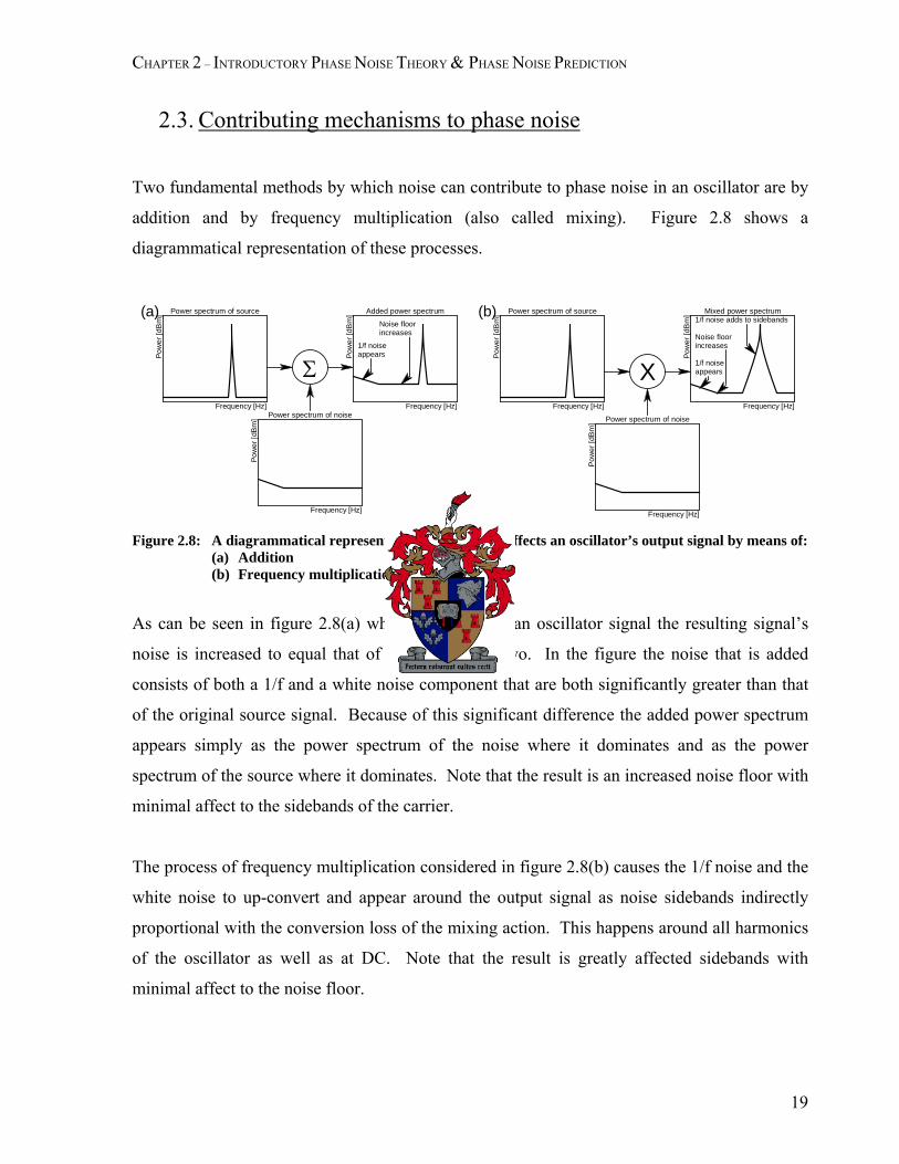
Two fundamental methods by which noise can contribute to phase noise in an oscillator are by
addition and by frequency multiplication (also called mixing). Figure 2.8 shows a
diagrammatical representation of these processes.
Σ
Pow
er [d
Bm
]
Frequency [Hz]
Pow
er [d
Bm
]
Frequency [Hz]
Power spectrum of source
Power spectrum of noise
(a)
Frequency [Hz]
Pow
er [d
Bm
] Added power spectrum
1/f noiseappears
Noise floorincreases
X
Pow
er [d
Bm
]
Frequency [Hz]
Pow
er [d
Bm
]
Frequency [Hz]
(b) Power spectrum of source
Power spectrum of noise
Frequency [Hz]
Pow
er [d
Bm
]
1/f noiseappears
1/f noise adds to sidebands
Noise floorincreases
Mixed power spectrum
Figure 2.8: A diagrammatical representation of how noise affects an oscillator’s output signal by means of:
(a) Addition (b) Frequency multiplication (or mixing)
As can be seen in figure 2.8(a) when noise adds to an oscillator signal the resulting signal’s
noise is increased to equal that of the sum of the two. In the figure the noise that is added
consists of both a 1/f and a white noise component that are both significantly greater than that
of the original source signal. Because of this significant difference the added power spectrum
appears simply as the power spectrum of the noise where it dominates and as the power
spectrum of the source where it dominates. Note that the result is an increased noise floor with
minimal affect to the sidebands of the carrier.
The process of frequency multiplication considered in figure 2.8(b) causes the 1/f noise and the
white noise to up-convert and appear around the output signal as noise sidebands indirectly
proportional with the conversion loss of the mixing action. This happens around all harmonics
of the oscillator as well as at DC. Note that the result is greatly affected sidebands with
minimal affect to the noise floor.
19

CHAPTER 2 – INTRODUCTORY PHASE NOISE THEORY & PHASE NOISE PREDICTION
Although both figures 2.8 (a) and (b) show the output as power spectra it must be remembered
that the phase noise and the amplitude noise contribute equally to the power spectrum so that
the phase noise would be proportionally affected.
Through modulation low frequency noise within the modulation bandwidth is frequency
translated to appear as phase noise around the carrier. When oscillators are powered by power
supplies rich in low-frequency noise such noise is known to contribute to the phase noise. For
this reason batteries are often used to power low phase noise oscillators as they are considered
to provide minimal low-frequency noise.
2.4. Generally available phase noise models
Much literature is available on the subject of phase noise modelling. Of the available literature
on the subject, all the models can be categorised according to the assumptions governing these
models. This allows for most phase noise models to be grouped into one of three classes. In
order of increasing complexity, generality and accuracy these classes are: linear time-invariant
(LTI), linear time-variant (LTV) and non-linear time-variant (NLTV).
The most trusted and most widely applied phase noise model of each of these classes of phase
noise modelling is now discussed. After every model is discussed, the usefulness of the
particular model to the design of low phase noise oscillators is considered.
This section concludes with a tabular comparison of the three phase noise models concerned.
20

CHAPTER 2 – INTRODUCTORY PHASE NOISE THEORY & PHASE NOISE PREDICTION
2.4.1.Leeson’s model
In 1966 D. B. Leeson proposed a model with which to predict phase noise of oscillators, [13].
That model will be briefly discussed in this section.
Leeson’s model is governed by both linearity and time-invariant assumptions putting it into the
family of LTI (linear time-invariant) models. Leeson’s much referenced equation is given
below:
( ) ⎟⎟⎠
⎞⎜⎜⎝
⎛⋅
+⋅⋅⎥
⎥⎦
⎤
⎢⎢⎣
⎡⎟⎟⎠
⎞⎜⎜⎝
⎛+=
inL PFkT
ffQff
2221
2
0
παL (2.16)
where – is the fundamental frequency of oscillation (in rad/s) of the oscillator 0f – frequency offset from the carrier (in rad/s) f
BfQL 2
2 0π= – the loaded quality factor of the resonator in the oscillator (B is the half-
bandwidth of the resonator) α – proportionality constant determined by fitting Leeson’s model to measured data F – effective noise figure of the oscillator (which, despite the terminology, is not the
same as the noise figure of a transistor) determined by circuit analysis or numerical circuit simulation
– Boltzmann’s constant (≈ 1.380658x10⁻²³ J/K) k – noise temperature (in kelvin) T – power of signal at input to active element in oscillator inP
From equation 2.16 it can be noted that the expected behaviour of phase noise with frequency
can be divided into three regions when plotted on a log-log scale:
For offset frequencies far away from the carrier: In this region there is no frequency
dependence so that the noise behaviour in this region can be described as the white noise floor
(or simply as the noise floor) of the oscillator. This region is also called the ultimate phase
noise since it places a lower limit on what the achievable phase noise is for a given oscillator.
A graphical depiction of this region can be found on the far right-hand side in figure 2.9. In
this region the phase noise is determined by the last term of the second factor in Leeson’s
equation, equation 2.16:
21

CHAPTER 2 – INTRODUCTORY PHASE NOISE THEORY & PHASE NOISE PREDICTION
( ) ( ) [ ininN
floor PP
FkTthermal
torelative ratio a as1421
⎟⎟⎠
⎞⎜⎜⎝
⎛⋅⋅⎟
⎠⎞
⎜⎝⎛= 321L ] (2.17)
This expression is most useful when expressed on a normalised logarithmic power scale:
( ) [ ]
[ ]dBc/Hz001.02
log10
dBc/Hzofunitsin01.3
10 indB
indBthermalfloor
PFkT
PFN
−+⎟⎠⎞
⎜⎝⎛
×⋅=
−+−=L (2.18)
2/1 f -region: In this region the phase noise falls with 6dB/octave as the offset frequency from
the carrier increases. This behaviour is observed for offset frequencies that are not far from the
carrier, nor too close to the carrier.* Figure 2.9 shows the phase-frequency relation in this
region in the middle of the graph. The corner frequency between the flat noise floor region and
the -region is dependent on the loaded quality factor of the resonator, . This point on
the frequency axis may be calculated:
2/1 f LQ
LL
cornerf Qf
QfBf 00
1 22
2
⋅=
⋅⋅⋅
==−
ππ (2.19)
* Although this description is very vague, it is sufficient for this qualitative discussion. The parameters in Leeson’s model that determine these exact corner frequencies are QF and ,α . Of these parameters both
F and α are determined by fitting Leeson’s model to oscillator measurements.
22

CHAPTER 2 – INTRODUCTORY PHASE NOISE THEORY & PHASE NOISE PREDICTION
This corner frequency may be used to predict the phase noise in the -region if this region
occurs for :
2/1 f
Hzf 1≥
( ) ( ) ( ) [ ]dBc/Hzofunitsinlog20log20 22 110101 cornerffloorregionf fff
−−⋅++⋅−= LL (2.20)
For offset frequencies close to the carrier (where oscillator is non-linear): Closer to the carrier
Leeson’s phase noise model predicts that the phase noise power spectrum will deteriorate with
at 9dB/octave slope with the offset frequency (this is a -decline) and is illustrated on the
far left side in figure 2.9.
3/1 f
These predictions agree well with observations. For offset frequencies that are very close to
the carrier Leeson’s model does not hold since other factors that were ignored for simplicity’s
sake in the deduction of Leeson’s model come to dominate in this region.
Slope = -9dB/octave
Slope = -6dB/octave
Phase noise ( L(f) ) as predicted by Leeson's model
Phas
e no
ise
[dB
c/H
z]
Logarithmic offset frequency [Hz]
α ( f0 / 2QL)2( f )-3
f1/f 2-corner= ( π f0 ) / QL
( f0 / 2QL)2[FkT/(2Pin)]( f )
-2
FkT/(2Pin)
Figure 2.9: Leeson's model provides an asymptotic approximation over three regions of phase noise
decline with frequency
23

CHAPTER 2 – INTRODUCTORY PHASE NOISE THEORY & PHASE NOISE PREDICTION
2.4.1.1. Conclusion on Leeson’s model:
Leeson’s model assumes only linearity which allows the application of the superposition
principle to yield three solutions for distinct frequency ranges which can then be combined into
a single solution. Since oscillators are inherently non-linear, it is expected that such a linear
phase noise model would predict the phase noise of an oscillator with a significant error.
However, Leeson’s model accommodates non-linear oscillator behaviour by incorporating the
effective noise factor of the oscillator, F (which is a parameter describing phase noise
contributed by the active part of the oscillator and must not be confused with the noise figure
of a transistor since these two parameters describe different noise contributions). This does not
free the model of its linear restrictions; the model remains essentially linear since the principle
of superposition is applied in its derivation.
This effective noise factor of the oscillator, F, is determined by circuit analysis or by breaking
the feedback loop of the oscillator and terminating the ends in loads equivalent to closed loop
conditions and using a computer circuit simulator to find the open-loop noise figure of the
system.
Leeson’s phase noise model remains the simplest and most often referenced phase noise model
in literature. Leeson’s model allows for a closed form analysis of phase noise which relates the
physics of the circuit to the phase noise – a property which all other phase noise models lack.
Such an analysis gives the designer tangible insight into the operation of the oscillator and its
relation to phase noise, which is the central theme of this thesis.
An immediate consequence of Leeson’s equation, equation 2.16, is that the phase noise can be
reduced by increasing the loaded quality factor, QL, of the resonator and the power of the
oscillation signal, Pin. By raising the power of the oscillation signal the reference is raised
(although the noise floor does not become lower, it drops relative to the oscillation signal
power – as phase noise is expressed in dB relative to the carrier per Hz) resulting in reduced
phase noise.
24

CHAPTER 2 – INTRODUCTORY PHASE NOISE THEORY & PHASE NOISE PREDICTION
Another limitation to be remembered is that the phase noise closest to the carrier that Leeson’s
model provides for is -noise (as observed from equation 2.16 or figure 2.9). Closer to the
carrier stricter band-limited noise ( *
3/1 f
1for /1 2 >+ nf n ) dominates so that the usefulness of this
model is limited in such cases.
2.4.2.Lee & Hajimiri’s model
Unsatisfied with previous phase noise models, T. H. Lee and A. Hajimiri challenged the time-
invariance assumption governing prior LTI phase noise models to construct a linear time-
variant (LTV) phase noise model that would yield quantitative results [1], [11], [15].
After pointing out the linear relation between an injected noise current impulse and the
resulting phase error by computer simulation, this model proposes the use of an impulse
response (noise current-to-phase) transfer function to completely characterise the phase error of
an oscillator in terms of noise current sources.
Furthermore it is shown that the phase error produced by an injected noise impulse is
dependent on the phase at which (i.e. when in the oscillation cycle†) such an impulse is injected
into the system. This leads to the introduction of an impulse sensitivity function (ISF) which
weighs the effect that the injected noise current would contribute (depending on when in the
oscillation cycle it was injected) to the phase of the output signal in the noise current-to-phase
transfer function which was mentioned earlier.
The ISF is a function that can only be constructed analytically in a few special cases and must
otherwise be found through computer simulation. Since it is a weighing function, its amplitude
must vary between -1 and 1 and its cyclic behaviour usually approximates well using only the
first few terms of a Fourier series.
* This was illustrated in figure 2.7(b). † This time dependence violates the time-invariant assumptions governing LTI phase noise models making Lee & Hajimiri’s model time-variant (LTV).
25

CHAPTER 2 – INTRODUCTORY PHASE NOISE THEORY & PHASE NOISE PREDICTION
By far the most significant insight credited to this model is summarised in the following
statement. The expression of the noise current-to-phase transfer function in terms of the
Fourier series of the ISF clearly shows that any perturbations in the noise current found close to
integer multiples of the oscillation frequency (which includes perturbations close to DC) are
frequency translated to the oscillation frequency. This allows for the calculation of phase noise
caused by a noise source whose power density spectrum exhibits any frequency dependence
(i.e.: ). Practically, this statement is valuable to the design of low
phase noise oscillators because it implies that the phase noise performance of an oscillator can
be improved if noise close to DC and close to integer multiples of the carrier can be
suppressed.
0 for /1 ∪ℵ∈nanyf n
When the noise current causing the phase perturbation is considered, it is concluded that the
limiting behaviour in oscillators drives the active element(s) in the circuit into non-linear
regions where the concerned noise current performs differently to when the active element(s) is
in its linear region. Since this occurrence is cyclic (usually with the oscillation frequency or its
second harmonic), the statistical behaviour of the noise current displays a similar cyclic
recurrence which is described as cyclostationary*. When a cyclostationary noise source is
applied to the noise current-to-phase transfer function it is noted that this cyclostationary
behaviour can be mathematically attributed to the ISF instead without effect on the transfer
function. This further complication of cyclostationary modelling may thus be simplified by
considering an effective ISF that incorporates the cyclostationary behaviour.
Finally Lee & Hajimiri’s model proposes two equations that can be used to find the phase noise
in various frequency-dependent ranges due to multiple noise sources present at multiple nodes
in an oscillator. Equation 2.21 below describes the phase noise power spectrum due to a white
noise current source which yields an equation that describes the noise in the
-frequency-dependent range: 2/1 f
* Behaviour where the value of a statistically random variable displays a cyclic recurrence with time is described as cyclostationary [1] & [11].
26

CHAPTER 2 – INTRODUCTORY PHASE NOISE THEORY & PHASE NOISE PREDICTION
( )⎟⎟⎟⎟⎟
⎠
⎞
⎜⎜⎜⎜⎜
⎝
⎛
Δ⋅Γ
≈ 2
2
2max
2
4log10
m
n
rmsm
fi
q ωωL (2.21)
where – rms value of the ISF, rmsΓ Γ – which is found by computer simulation and
through subsequent application of the equation:
( )∫∑ Γ=Γ=∞
=
π
π2
0
22
0
2 21rms
mn dxxc , rmsΓ may be solved for
maxq – maximum charge displacement of the capacitor in the LC-resonator for a noise current source in parallel with a capacitor. For the case where a noise voltage source in series with an inductor is considered, is replaced with
, where maxq
maxmax LI=Φ maxΦ is the maximum magnetic flux deviation in the inductor; after which the equation holds for the equivalent current noise source found through source transformation.
fin
Δ
2
– power contribution (per Hz bandwidth) ascribed to a white noise current source
In the -frequency-dependent range, the phase noise power spectrum can be
found as:
ℵ∈+ kf k for /1 2
( )⎟⎟⎟⎟⎟
⎠
⎞
⎜⎜⎜⎜⎜
⎝
⎛
⋅Δ≈ km
f
m
mn
m
k
q
cf
i
ω
ω
ωω /1
22max
22
4log10L (2.22)
where km
fnfn
k
k fii
ω
ω /12
2/1, ⋅
Δ= – the phase noise power contribution made by the noise
current source (per 1 Hz bandwidth) kf/1ω – corner frequency which can be calculated from the ISF, Γ kf/1
– a coefficient which follows from the Fourier-series approximation of the ISF, Γ
mc
A procedure may be formulated according to which the theory of Lee & Hajimiri’s model
would predict the phase noise for an oscillator which is modelled with multiple noise sources.
Such a procedure is presented in three steps and centres on the application of equations 2.21
and 2.22:
27

CHAPTER 2 – INTRODUCTORY PHASE NOISE THEORY & PHASE NOISE PREDICTION
1. Ensure that all noise sources are expressed as noise current sources through source
transformations if necessary. Identify each noise current source as correlated or
uncorrelated with respect the others.
2. Find the phase noise power contribution from the appropriate equation (either 2.21
for white noise current or 2.22 otherwise) by finding the ISF, Γ (usually through
computer simulation)
3. For uncorrelated noise current sources, the resulting phase noise contribution is the
sum of the phase noise power spectra. For correlated groups of noise current
sources: square the sum of phase noise rms values. Finally the contributions from
both classes of correlation can be added to yield the phase noise power spectrum
resulting from all the sources.
2.4.2.1. Conclusion on Lee & Hajimiri’s model:
At first glance it seems as if the Lee & Hajimiri-model overcomes all of the shortcomings of
Leeson’s phase noise model. Lee & Hajimiri’s model predicts the phase noise power spectrum
quantitatively (even close to the carrier) for any gradient (phase noise power spectrum of
gradient as caused by a noise current source with power spectrum
of gradient ). Furthermore, all the noise sources present in the oscillator – even
cyclostationary noise sources – can be fully taken into account.
0 for /1 2 ≥•∈+ ZZkanyf k
kf/1
Careful inspection of the Lee & Hajimiri-model reveals that there are difficulties with its
application to phase noise prediction. This follows since, apart from the ISF, the expression for
the phase noise contains no dependence at all regarding the physics of the oscillator (circuit
parameters e.g. capacitances, inductances, resistances, transistor parameters, etc.). In order to
obtain a quantitative phase noise solution for a circuit, the ISF has to be calculated by computer
simulation on the oscillator circuit. Since analytical solutions for the ISF in terms of circuit
parameters are mostly non-existent, it can only be done numerically. Consequently insight into
how the physics of the circuit (the circuit parameters) can be manipulated to yield improved
phase noise performance is lost.
28

CHAPTER 2 – INTRODUCTORY PHASE NOISE THEORY & PHASE NOISE PREDICTION
This model does yield some insights that previous phase noise models overlooked. Firstly it
reveals that if the active element in an oscillator were able to instantaneously restore dissipated
energy to the resonator at precisely the right moment in the oscillation cycle, then it would in
principle be possible to limit the phase noise to a minimum. This conclusion is supported by
Lee & Hajimiri ([1], [11]) by examination of the Colpitts-oscillator which is shown to
approximate this behaviour relative to other oscillator configurations.
Secondly this model shows that the phase noise can be reduced by increasing the maximum
charge displacement, , in equations 2.21 & 2.22. This can in some cases be physically
accomplished by increasing the output power level of the oscillation signal – although this
insight is more specific it is something already known from Leeson’s model.
maxq
Thirdly, any phase noise present around integer multiples of the oscillation frequency is
frequency translated to appear as phase noise sidebands around the oscillation signal.
Specifically, this points out the importance of powering the oscillator with a DC-supply that is
free from low frequency noise.
Various other conclusions are drawn that amount to manipulation of the ISF, but such
conclusions are removed from what can be implemented through oscillator circuit design.
Lee & Hajimiri’s phase noise model is a generalisation on Leeson’s model if it is evaluated at
the hand of underlying assumptions but it is a step closer to numerical computer simulation at
the cost of analytical insight bound to physical parameters. While Leeson’s model retained the
loaded quality factor of the resonator (a physical parameter), Lee & Hajimiri’s model does
away with as many of the physical circuit parameters as possible (unifying the effect of such
parameters into a single ISF). In so doing valuable insight that its retention could have brought
to the phase noise dependence on such parameters is lost.
29

CHAPTER 2 – INTRODUCTORY PHASE NOISE THEORY & PHASE NOISE PREDICTION
2.4.3.Demir, Mehrotra & Roychowdhury’s model
Demir, Mehrotra & Roychowdhury, [6], pointed out that all phase noise models governed by
linearity assumptions (whether LTI or LTI) lead to the conclusion that both the total integrated
power and the noise power density at the carrier are infinite – a physical impossibility. This
discrepancy led them to challenge the linearity assumption governing previous phase noise
models to develop a nonlinear time-invariant (NLTI) phase noise model from the fundamental
differential equation description for a general* oscillator by taking noise perturbation signals
into account.
Although the only noise signals taken into account are from white noise and modulated-white
noise sources, reference is made to literature that would lead to a similar development for noise
sources with a power spectrum falling as (as well as for modulated sources
of such frequency dependence). It is proved that such white noise and modulated-white noise
sources lead to a phase deviation,
ℵ∈kanyf k for /1
( )tα , which is probabilistically characterised as being a
stochastic process with characteristic function, ( )tF ,ω . This characteristic function, ( )tF ,ω , is
shown to be a Gaussian random variable asymptotically with time so that it can be completely
described by a mean, ( )tμ , and a variance, ( )tσ . For such white noise and modulated white
noise sources, the phase noise power spectrum is analytically derived as:
( )( ) ( )∑
∞
−∞= ++=
iii ici
ciXXS 20
240
220*
4/1 ωωωωω (2.23)
where – Fourier coefficients of the asymptotically orbitally stable periodic
solution
iX
† to the oscillation, ( )txs , such that: . ( ) ∑∞
−∞=
=i
tjiis eXtx 0ω
* This model is so general that it does not even need to be an electrical system. This model is valid for any physically realizable system (electrical, mechanical, biological, etc.) that exhibits stable oscillatory behaviour. † With asymptotically orbitally stable periodic solution is meant the n-dimensional stable limit cycle solution. The standard non-linear analysis technique of linearizing around a non-linear stable limit cycle solution is employed in the derivation of equation 2.23. Physically this means that ( )txs is simply the unperturbed oscillation signal.
30

CHAPTER 2 – INTRODUCTORY PHASE NOISE THEORY & PHASE NOISE PREDICTION
c – constant determined by: ( )[ ]tdtdc 2σ= , which physically translates to the rate of
change of the squared variance, σ , to the Gaussian solution of the characteristic function, , of the phase deviation, ( tF ,ω ) ( )tα .
oω – angular frequency of carrier signal
Demir, Mehrotra & Roychowdhury then continue to work toward the climax of their
publication which is the time-efficient numerical characterisation of phase noise in both the
time and the frequency domains and claim that their algorithmic solution is of computational
complexity: *( )nO and three orders of magnitude faster (more than 1800 times faster) than the
Monte Carlo method (which was the only alternative technique that produced similar results)
when applied to specific problems.
2.4.3.1. Conclusion on Demir, Mehrotra & Roychowdhury’s model
While this phase noise model is unequalled in its generality, accuracy and efficient
computational complexity, the physics of the circuit is completely lost by a pure statistical
characterization of the system. The parameter in equation 2.23 that is most closely related to
the physics of the circuit is the constant, , which is removed from the direct physics of the
circuit by three levels of abstraction . This loss prevents the phase
noise characterisation to reveal which circuit parameters can be manipulated to improve the
phase noise.
c
( ) ( ) ⎟⎟⎠
⎞⎜⎜⎝
⎛→→→ ctFt
levellevellevel 321
, σωα
Equation 2.23 shows a phase noise reduction with frequency and so qualitatively reveals
nothing more than what can be learned from linear phase noise models.
2/1 f
This phase noise model is well suited to computation of phase noise by computers, but poorly
suited to analytical computation by hand on paper. Demir, Mehrotra & Roychowdhury point
out that their time-domain phase noise algorithm becomes numerically unstable when the
* “Large circuits are handled efficiently, i.e., computation/memory scale linearly with circuit size”, as quoted from p. 657, [6]
31

CHAPTER 2 – INTRODUCTORY PHASE NOISE THEORY & PHASE NOISE PREDICTION
concerned oscillator employs a high Q resonator. Similarly, their frequency domain phase
noise algorithm depends on the numerical method of harmonic balance – a method which is
similarly known to be problematic when applied to oscillators with high Q resonators. Since
the electrical oscillators that yield the lowest phase noise depend on very high Q resonators,
this numerical characterization of phase noise breaks down when extremely low phase noise
oscillators are considered.
2.4.4.Conclusions and Comparisons of Phase Noise Models
A tabular summation pointing out the relative strengths and weaknesses of the three phase
noise models that were considered in this section is given in table 2.1 below.
Table 2.1: Comparative summation of typical LTI, LTV and NLTV phase noise models
Model Leeson Lee & Hajimiri Demir, et al. Assumptions LTI LTV NLTV Perturbing noise source
constant white noise ( ) kTB
cyclostationary ℵ∈kf k ,/1
modulated ℵ∈kf k ,/1
Accuracy reasonable good exact Simplicity simple moderate involved
Computer dependence
independent (calculable by hand)
need computer to calculate ISF
completely computer dependent (no closed form solutions)
Predicts close-in phase noise no yes yes
Retained circuit parameters SL PQ , maxq none
In their article, [6], Demir, Mehrotra & Roychowdhury refer to available literature on phase
noise: “Considerable effort has been expended over the years in understanding phase noise
and in developing analytical, computational and experimental techniques for its
characterization. Despite the importance of the problem and the large number of publications
on the subject, a consistent and general treatment and computational techniques based on a
sound theory appear to be still lacking.”* and again later: “In summary, the available
literature often identifies basic and useful facets of phase noise separately, but lacks a rigorous * p. 655 in [6]
32

CHAPTER 2 – INTRODUCTORY PHASE NOISE THEORY & PHASE NOISE PREDICTION
unifying theory clarifying its fundamental mechanism.”*. They proceed to make the claim that
their model overcomes these shortcomings.†
NLTV phase noise models are widely applied in open source, free and commercial software
packages and yield reliable phase noise predictions from circuit solvers for LC-oscillators. The
common approach is to repeatedly simulate the phase noise and change one circuit parameter at
a time until the required phase noise specification has been met. Such a design process allows
for a good intuition too be developed with respect to a specific oscillator circuit.
Unfortunately, no matter how well such an intuition is developed, such intuition alone cannot
explain why the phase noise is better or worse – it can only say whether or not an oscillator
would yield low phase noise or not. Such an intuition is also not conferrable to another person.
A more methodical approach is required.
To return to the statements quoted from [6], made by Demir, Mehrotra & Roychowdhury
previously: although it seems as if the NLTV theory fills all the shortcomings of previous
phase noise models, it fails to provide for the most important shortcoming from a design
perspective – which is an analytical, closed form solution by which phase noise can be related
to circuit physics.
The simplicity of the LTI phase noise model (as presented by Leeson) allows for the qualitative
analysis of oscillator circuits
* p. 658 in [6] † p. 655 in [6]
33

CHAPTER 2 – INTRODUCTORY PHASE NOISE THEORY & PHASE NOISE PREDICTION
2.5. Conclusion
The first part of this chapter was concerned with defining and expressing phase noise while
simultaneously developing some insight into the physical properties of signals exhibiting phase
noise. Theoretical models of phase noise that rely on linear time-invariant (LTI), linear time-
variant (LTV) and non-linear time-variant (NLTV) assumptions were considered and compared
from the perspective of a crystal oscillator designer.
The simplest phase noise model, Leeson’s model, is based on linear time-invariant
assumptions. It does not provide for phase noise prediction of non-linear oscillators. Increased
non-linear behaviour in oscillators can only cause the phase noise to increase compared to
oscillators that exhibit more linear behaviour. This is a consequence of the mechanisms of how
noise appears as phase noise sidebands around the carrier*. Non-linear behaviour increases
phase noise around a carrier as a consequence of frequency mixing action between the non-
linear operation of circuit components and low-frequency noise. Consequently, if a design goal
is to achieve the lowest possible phase noise care must be taken to ensure linear operation of as
much of the oscillator as possible. Because non-linear behaviour cannot be eliminated from
oscillatory systems, it must be managed in a manner that would least contribute to phase noise
for very low phase noise design systems.
More general phase noise models such as that of Lee & Hajimiri as well as that of Demir,
Mehrotra & Roychowdhury take into account the phase noise contribution of non-linear
oscillator behaviour. These models are most useful when considering the problem of how the
phase noise of a heavily non-linear oscillator can be improved. Application of such non-linear
phase noise models does not yield superior phase noise performance to oscillators that exhibit
more linear behaviour. This is again a consequence of the mechanism of how noise appear
around the phase noise sidebands of a carrier signal.
* This was considered in section 2.3.
34

CHAPTER 2 – INTRODUCTORY PHASE NOISE THEORY & PHASE NOISE PREDICTION
To conclude, it was found that predictive phase noise theories bring insights that are valuable
to the crystal oscillator designer in minimising the phase noise. Of the three phase noise
models that were considered, Leeson’s model is the most useful from a very low phase noise
design perspective as it yields the most insight into the phase noise dependence on the physics
of the oscillator circuit. In chapter 5 it will be shown how Leeson’s phase noise model can be
applied to the design of a low-phase noise crystal oscillator while chapter 6 will present phase
noise measurements on this circuit.
35

Chapter 3
Quartz crystal resonators: fundamental working, modelling and quality
factor
Oscillators which use quartz crystal resonators have a significant advantage over oscillators
that employ lower quality factor resonators such as LC-resonators. This section provides the
most relevant information regarding quartz crystal resonators and includes discussions on the
physics, measurement and modelling of quartz resonators as well as a brief comparison of the
two different crystal cuts that were used in this project (AT-cut and SC-cut).
3.1. Fundamental physics of quartz resonators
In 1880 the brothers Pierre & Jacques Curie showed that a potential difference is observed on
the surface of a quartz crystal when a weight is placed on it and that this measured potential
difference is proportional to the force applied to the crystal. In the following year it was shown
that inversely, when a potential difference is applied to a quartz crystal, the crystal deforms.
This mechanical-electrical relation that is observed in 20 of the 32 crystal classes is called the
piezo-electric effect – from the Greek word piezin (to press) [18], [19], [20], [21]. The piezo-
electric effect may be defined as electric polarisation produced by mechanical strain in
crystals belonging to certain classes, the polarisation being proportional to the strain and
changing sign with it [19].
This effect was first exploited for application to electrical resonators – using quartz
– in the 1920s when rapid developments in radio occurred. Although many crystals are known
to have piezo-electrical properties, quartz is one of the few that proved to be useful as electric
resonators [19], [20], [22].
Despite the natural abundance of quartz (SiO2), very pure natural quartz deposits that are
suitable for use in electrical resonator production have only been found in Brazil and
Madagascar. The purity of the crystals can be improved significantly by growing the crystals
36

CHAPTER 3 – A STRATEGY FOR INVESTIGATIONS INTO PHASE NOISE OF QUARTZ CRYSTAL OSCILLATORS
artificially using a hydro-thermal growth process. After silicon (Si) for use as semi-conductor
substrate, quartz is the crystal that is synthetically grown most with about 3000 tons being
produced annually worldwide (1997 data) [20]. Worldwide 2 billion quartz crystal resonator
units were sold annually with a total annual market value of $1.2 billion according to 2001 data
[18], [20], [22].
(a) (b) Figure 3.4: Visual representation of a quartz crystal:
(a) A right handed quartz crystal with orientation of axis (b) Photograph of a quartz crystal
Figure 3.4 (a) and (b) give a visual impression of quartz crystals. When ignoring the minor
faces of the crystal, its shape may be described as a hexagonal prism which is tapered to a point
by three major rhomb faces at each end. The z-axis – which is often called the optical axis – is
chosen in the same direction of the prism edges somewhere in the middle of the lattice. From
there the y-axis is chosen such that it is orthogonal with respect to one of the prism faces. The
x-axis would then bisect the angle made by two of the other prism faces. Since the physical
properties of the crystal is periodic with a 120° rotation about the z-axis, this choice of axis
leaves three different but equivalent choices of the axes [18], [19], [20].
Both left-handed and right-handed quartz crystals exist. These two forms are mirror images of
each other and cannot be made equivalent by simple rotation. Crystals with this property are
called enantiomorphic. When polarized light is passed through a quartz crystal along the
optical axis the direction of polarization is rotated. If the polarisation is rotated clockwise as
37
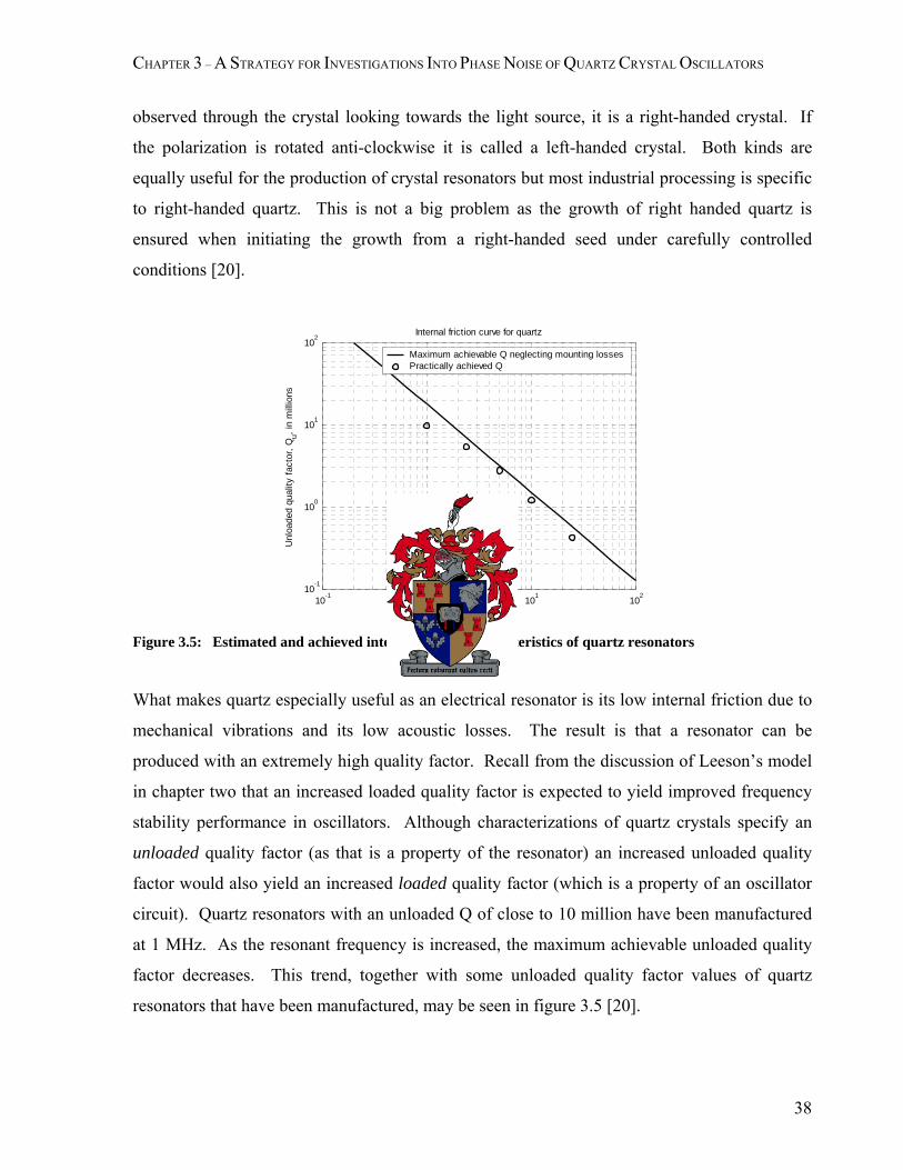
CHAPTER 3 – A STRATEGY FOR INVESTIGATIONS INTO PHASE NOISE OF QUARTZ CRYSTAL OSCILLATORS
observed through the crystal looking towards the light source, it is a right-handed crystal. If
the polarization is rotated anti-clockwise it is called a left-handed crystal. Both kinds are
equally useful for the production of crystal resonators but most industrial processing is specific
to right-handed quartz. This is not a big problem as the growth of right handed quartz is
ensured when initiating the growth from a right-handed seed under carefully controlled
conditions [20].
10-1
100
101
102
10-1
100
101
102
Internal friction curve for quartz
Frequency [MHz]
Unl
oade
d qu
ality
fact
or, Q
u, in
mill
ions
Maximum achievable Q neglecting mounting lossesPractically achieved Q
Figure 3.5: Estimated and achieved internal friction characteristics of quartz resonators
What makes quartz especially useful as an electrical resonator is its low internal friction due to
mechanical vibrations and its low acoustic losses. The result is that a resonator can be
produced with an extremely high quality factor. Recall from the discussion of Leeson’s model
in chapter two that an increased loaded quality factor is expected to yield improved frequency
stability performance in oscillators. Although characterizations of quartz crystals specify an
unloaded quality factor (as that is a property of the resonator) an increased unloaded quality
factor would also yield an increased loaded quality factor (which is a property of an oscillator
circuit). Quartz resonators with an unloaded Q of close to 10 million have been manufactured
at 1 MHz. As the resonant frequency is increased, the maximum achievable unloaded quality
factor decreases. This trend, together with some unloaded quality factor values of quartz
resonators that have been manufactured, may be seen in figure 3.5 [20].
38

CHAPTER 3 – A STRATEGY FOR INVESTIGATIONS INTO PHASE NOISE OF QUARTZ CRYSTAL OSCILLATORS
Figure 3.6: Orientation of a quartz crystal resonator wafer relative to the crystal axes
Quartz is an anisotropic crystal. This means that its physical characteristics differ significantly
with the direction of the axes. Among others, characteristics which are heavily dependent on
the crystallographic direction are the etching rate, the thermal expansion coefficient, the elastic
modulus coefficients and the modes of vibration. This highly anisotropic nature of quartz
makes it possible to design quartz resonators to meet specific requirements by simply
controlling the angles relative to the crystal axes at which a wafer of quartz for use as a
resonator is cut from its source crystal. There are two angles that may be used for such design
purposes and these are shown in figure 3.6. The first is the angle of the wafer relative to the
optical axis (i.e. the z-axis) and this angle is called, θ . The second angle is the angle of the
wafer relative to the x-axis which is called, φ . The angles are almost without exception chosen
on a locus that yields zero temperature coefficient resonators – this minimizes frequency drift
with temperature variation. Few crystals other than quartz can be used to produce resonators
with a zero temperature coefficient [19], [20], [21].
Choosing for instance '1535°≈θ and °≈ 0φ yields the commonly used AT-cut resonators. As
the angle °≈ 0φ , the AT-cut crystal is a singly rotated cut. The manufacture of such
resonators that only has a single significant rotational dimension is greatly simplified. As a
result such crystals are much more commonly available and are also much cheaper than doubly
rotated crystals. In contrast to this, SC-cut (SC is the abbreviation for stress compensated)
resonators are cut at angles '1535°≈θ and '5421°≈φ . Manufacturing processes that cut
39

CHAPTER 3 – A STRATEGY FOR INVESTIGATIONS INTO PHASE NOISE OF QUARTZ CRYSTAL OSCILLATORS
quartz crystals relative to two crystallographic axes with sufficient precision are more
complicated. Consequently such resonators are more expensive and are often made on special
request only. Doubly rotated resonators can be made superior to singly rotated resonators in
almost every significant respect simultaneously: unloaded quality factor, frequency-
temperature stability, series resistance, etc. Often such improvements are of an order of
magnitude or more for more than one critical attribute simultaneously. Such advantages are
pointed out at the end of section 3.2.3. Depending on the requirements of the resonator, the
high cost of doubly rotated quartz resonators may well be justified.
Figure 3.7: Modes of vibration of quartz crystal wafers [22]
A further physical parameter which is determined by the orientation of the cut is the mode of
vibration. This parameter deserves special attention as it determines which dimensions of the
quartz wafer would establish its resonant frequency. Figure 3.7 shows the modes of vibration
which resonators of different quartz cuts exhibit as well as their available frequency ranges.
The frequency of such a resonator may be increased by decreasing the dimension(s) most
critical to the mode of vibration, e.g. the resonant frequency of a thickness shear resonator may
be increased by making the wafer thinner. Another method of increasing the resonant
frequency is by exciting a higher order vibration in the resonator. Thickness shear resonators
that operate at their fifth or seventh overtone are commercially available up to 360 MHz. It has
been reported in personal correspondence to the author by a senior crystal resonator design
engineer at Nofech Electronics, Ltd. that use of a thickness shear resonator at its third overtone
yields a superior unloaded quality factor relative to all other overtones or the fundamental. By
exciting the resonators through electrodes that are carefully placed on the resonant zeros
mechanical losses can be limited – thus maximizing unloaded quality factor values. [18], [19],
[20], [21], [22].
40

CHAPTER 3 – A STRATEGY FOR INVESTIGATIONS INTO PHASE NOISE OF QUARTZ CRYSTAL OSCILLATORS
20 40 60 80 100 120 140-20
-15
-10
-5
0
5
10
15
T0
Typical frequency-temperature characteristic of quartz resonators
Temperature [deg. celcius]
Freq
uenc
y de
viat
ion
from
f 0 [p
pm]
Figure 3.8: Typical frequency-temperature characteristic curves for quartz resonators
The final resonator characteristic that needs closer attention is the frequency-temperature
relationship. This relationship for most quartz crystal resonators is often modelled by a third
order polynomial. Some typical frequency-temperature characteristic curves are shown in
figure 3.8. The inflection point of each curve is called its turnover temperature (TO) and is
labelled on figure 3.8 (located for this case at T=82˚C). As the angles of the resonator cut
relative to the crystallographic axes change slightly, so does the slope around TO. Crystals
which exhibit extreme frequency stability very close to their TOs may be designed by choosing
the angles such that this slope is zero precisely at TO. Consequently such resonators are most
useful when operating close to their inflection temperature and are often heated by a
temperature controller to ensure the maintenance of this condition. Oscillators that use such
temperature controlled resonators are called oven controlled crystal oscillators (OCXO).
Crystals whose frequency-temperature slope close to its TO is high may be frequency stabilised
by temperature control close to one of its other two turning points. Different crystal cuts yield
different TOs. Crystals with TOs close to room temperature are very popular and are
41

CHAPTER 3 – A STRATEGY FOR INVESTIGATIONS INTO PHASE NOISE OF QUARTZ CRYSTAL OSCILLATORS
sometimes employed where very frequency-stable resonators are required by application of
temperature compensation. This temperature compensation may be either actuated through a
temperature sensor setting the frequency of the oscillator (which then needs to be frequency
adjustable through a control voltage) or by compensation by a microcomputer. Oscillators that
use the compensation strategy to improve frequency stability are called temperature
compensated crystal oscillators (TCXO). [18], [19], [20], [21].
An effect called aging which is the long term (as measured over months and years) tendency of
the resonator to change frequency in one direction – either moving monotonously up in
frequency or moving monotonously down. This aging effect usually shows a decline so that
the resonator becomes increasingly stable over time. Usually this aging effect is very small,
typically 1-10 parts-per-million (ppm) over the first year depending on the quality of the
resonator. The cause of aging is not well understood and is usually attributed to contamination
of the resonator by slow gas leaks from the environment into the casing or long term stress
relief of the crystal on its mounting. In order to minimize this effect, great care and effort is
invested in making sure that the resonator wafers are as clean as possible at all times and that it
is contained in a gas-tight casing before being sold. Other causes of aging include changes in
the crystal mounting, changes to some of the elasticity coefficients induced by long term
stresses on the resonator or any other irreversible disturbances to the immediate environment of
the crystal (inside the casing). [19], [20], [21]
This subsection concludes with a list of factors that would affect a quartz crystal resonator’s
frequency stability in order of precedence without an in-depth discussion of each. Some of
these factors have already been discussed above, but are repeated in this list for completeness
sake. It is furthermore indicated whether each factor affects the short-term or long-term
frequency stability of the resonator. In most cases of oscillator design where quartz crystals are
used it is wise to limit all of these factors to a minimum where possible [18], [19], [20], [21],
[22].
42

CHAPTER 3 – A STRATEGY FOR INVESTIGATIONS INTO PHASE NOISE OF QUARTZ CRYSTAL OSCILLATORS
• Temperature (intermediate-term & long-term). Typical frequency deviation: 0.01-10 ppm/˚C depending on the frequency-temperature characteristic and the absolute temperature involved.
• Drive energy (short-term & long-term). Exceedingly much drive energy over the long-term may destroy the resonator. Typical frequency deviation: 1 ppm/mW change.
• Any mechanical force that the crystal is subjected to: gravity, acceleration, shock, mechanical vibration & acoustic vibration (short-term). This is the direct result of the piezo-electric effect. Typical frequency deviation: 0-0.3 ppm/N change
• Aging (long-term). Typical frequency deviation: 1-10 ppm/annum • Ionizing radiation (short-term & long-term) e.g. X-rays, γ-rays,
neutron/proton/electron radiation. Typical frequency deviation vary greatly with radiation type, it is often non-linear with radiation intensity and exposure. Neutron radiation causes irreversible damage to the resonator.
• Atmospheric conditions (intermediate-term & long-term): air pressure & humidity. These effects are often eliminated by air-tight packaging of the resonator.
3.2. Modelling and measurement of resonators
Circuit diagramsymbol for a
crystal resonator
X1 ba
L1
Electrical model of a crystalresonator at fundamental
or overtone frequency
C0
C1 R1
a b
Figure 3.9: Circuit diagram symbol and electrical model of a quartz crystal resonator
Electrically, quartz crystal resonators are simply modelled close to their fundamental resonant
frequency or close to any one of their overtones by the circuit diagram shown in figure 3.9.
The capacitance, C0, shown in figure 3.9 is the combined result of the capacitance between the
electrical contacts on which the resonator is also mechanically mounted inside a casing and the
capacitance between the pins that connect the resonator through the casing to the outside world.
The capacitance, C0, is commonly referred to as the static capacitance as it is not the
consequence of any mechanical vibration. The elements C1, L1 and R1 are called the motional
capacitance, the motional inductance and the series resistance respectively and are the result
of mechanical vibrations of the resonator which, through the piezo-electrical effect, may be
thus modelled electrically [18], [19], [20], [21], [22].
43
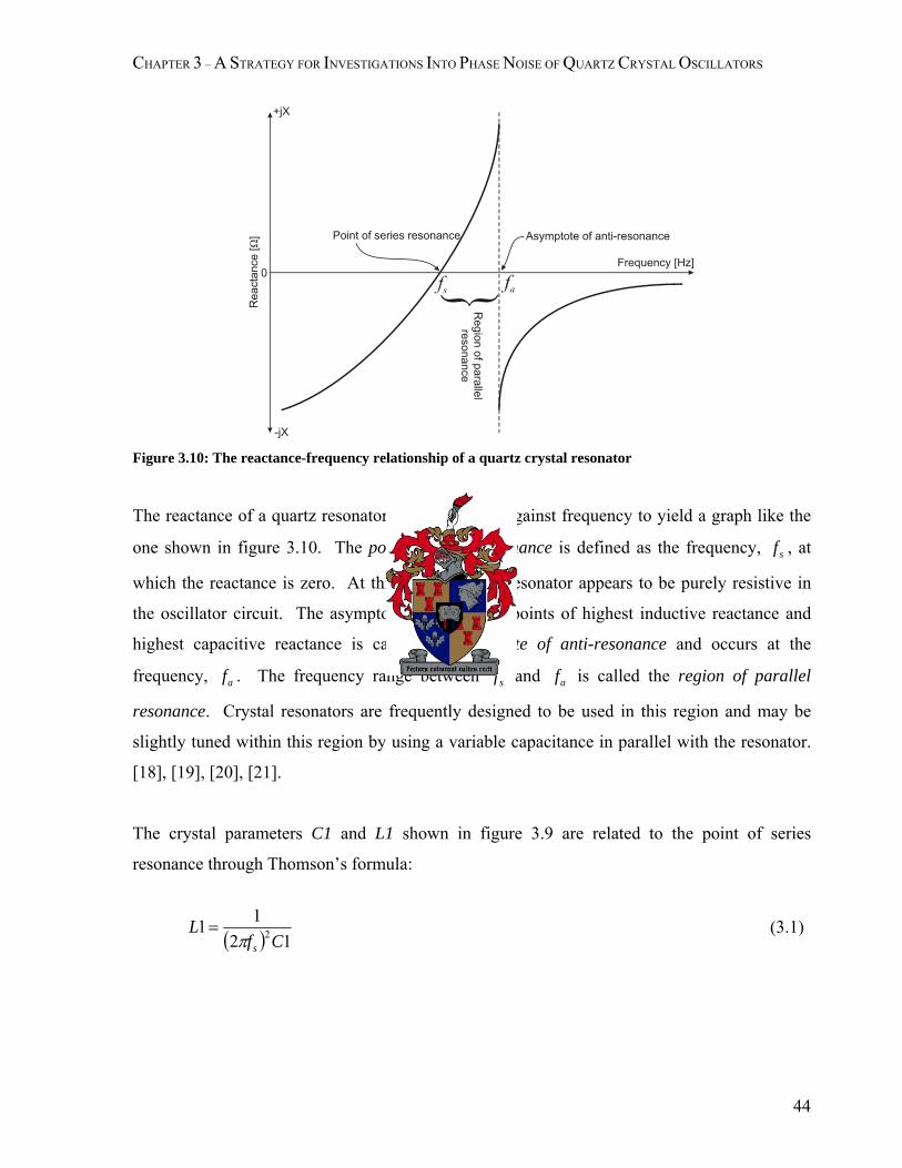
CHAPTER 3 – A STRATEGY FOR INVESTIGATIONS INTO PHASE NOISE OF QUARTZ CRYSTAL OSCILLATORS
Figure 3.10: The reactance-frequency relationship of a quartz crystal resonator
The reactance of a quartz resonator may be plotted against frequency to yield a graph like the
one shown in figure 3.10. The point of series resonance is defined as the frequency, , at
which the reactance is zero. At this frequency the resonator appears to be purely resistive in
the oscillator circuit. The asymptote that joins the points of highest inductive reactance and
highest capacitive reactance is called the asymptote of anti-resonance and occurs at the
frequency, . The frequency range between and is called the region of parallel
resonance. Crystal resonators are frequently designed to be used in this region and may be
slightly tuned within this region by using a variable capacitance in parallel with the resonator.
[18], [19], [20], [21].
sf
af sf af
The crystal parameters C1 and L1 shown in figure 3.9 are related to the point of series
resonance through Thomson’s formula:
( ) 1211 2Cf
Lsπ
= (3.1)
44

CHAPTER 3 – A STRATEGY FOR INVESTIGATIONS INTO PHASE NOISE OF QUARTZ CRYSTAL OSCILLATORS
When specific oscillators are studied, the ratio of the loaded to the unloaded resonator quality
factor is often stated as a percentage. This is considered to be a measure of how effectively an
oscillator circuit can exploit the quality factor of the resonator. The series resistance, R1,
shown in figure 3.9 is the result of the cut of the crystal resonator in question. SC-cut crystals
have a much higher series resistance than AT-cut crystals. This higher series resistance does
not force the quality factor lower as the motional capacitance, C1, of the SC-cut crystals
actually leads to the superior quality factor performance that the SC-cut crystals are known for.
Contrary to expectation perhaps, this higher series resistance of the SC-cut crystals means that
– for the same oscillator circuit – the intrinsic series resistance that the circuit forces onto the
crystal affects the crystal with the higher series resistance (in this case the SC-cut crystal) less
(than it would the AT-cut crystal). Consequently the resonator with the higher series resistance
bears less load relative to its own series resistance and exhibits a superior loaded quality factor,
i.e. the ratio of the loaded to the unloaded resonator quality factor is higher for resonators with
higher series resistances. [18], [20]
The unloaded quality factor of a crystal resonator may be expressed in terms of the equivalent
electrical model parameters that were shown in figure 3.9 and the point of series resonance,
[20], [21]:
sf
( )( )( )1121
CRfQ
sU π= (3.2)
In accordance with the Electronic Industries of America (EIA) standard EIA-512, resonator
parameter extraction is performed after calibrated and error corrected scattering parameter
measurements of the resonator on a vector network analyser according to the following
procedure. Accepting that the resonator can be sufficiently modelled by the electrical model of
figure 3.9, one port (with one resonator pin connected to ground) calibrated scattering
parameter measurements are taken around the resonant frequency. From these measurements
the admittance at each frequency may be calculated using the equation:
45

CHAPTER 3 – A STRATEGY FOR INVESTIGATIONS INTO PHASE NOISE OF QUARTZ CRYSTAL OSCILLATORS
⎟⎟⎠
⎞⎜⎜⎝
⎛⋅⎟⎟⎠
⎞⎜⎜⎝
⎛+−
=011
11 111
ZSSY (3.3)
where – one port measured, calibrated and error corrected scattering parameter 11S – characteristic impedance of the measurement system 0Z
In addition, the admittance of the electrical model of figure 3.9 when one of the two ports is
grounded (as is done for the scattering parameter measurement required by equation 3.3) may
be calculated as:
( ) ( ) ( )
( )( ) ( )
( ) ( ) ( ) ⎟⎟⎟⎟⎟
⎠
⎞
⎜⎜⎜⎜⎜
⎝
⎛
⎥⎦
⎤⎢⎣
⎡⋅
−⋅+
⋅−⋅
−⋅⋅+
⎥⎦
⎤⎢⎣
⎡⋅
−⋅+
= 22
22
1111
111
0
1111
1
CLR
CL
Cj
CLR
RY
ωω
ωω
ω
ωω
(3.4)
where – are the parameters corresponding to the model presented in
figure 3.9 1&1,1,0 RLCC
As equations 3.3 and 3.4 describe the same quantity, one from a measurement perspective and
one from a modelling perspective, these two equations must be identical. This allows one to
solve for all the model parameters of figure 3.9.
46

CHAPTER 3 – A STRATEGY FOR INVESTIGATIONS INTO PHASE NOISE OF QUARTZ CRYSTAL OSCILLATORS
Figure 3.11: Admittance measurement of resonator for model parameter extraction
It will now be illustrated how all these parameters may be solved for by considering the
admittance measurement of equations 3.3 and 3.4 graphically as seen in the solid line circle
plot of figure 3.11. Take note that the admittance measurement traces the outline of a circle in
the complex plane when measured at different frequency points close to the point of series
resonance of the resonator. This circle starts where the circle is tangent to the imaginary axis
and moves clockwise as the frequency is increased. This circle is in general located such that
the imaginary axis is tangent to the left edge of the circle and the centre of the circle is
somewhere in the first quadrant. To ensure accurate parameter extraction it is important that
many data points be taken – spaced closely in frequency around the series resonant point.
Some of these frequency points are marked with arrows on the solid line circle of figure 3.11.
In order of increasing frequency, the physical significance of these points is:
47

CHAPTER 3 – A STRATEGY FOR INVESTIGATIONS INTO PHASE NOISE OF QUARTZ CRYSTAL OSCILLATORS
Zfmin – frequency at which the resonator has least impedance
– point of series resonance if the capacitance is neglected sf 0C – point of zero-phase with low impedance 1f – point of zero-phase with high impedance 2f Zfmax – frequency at which the resonator has greatest impedance
From the measured data points a least squares fit of a circle to the data is performed by
computer. From this least squares fit the important characteristics of the circle are obtained:
the coordinates of its mid point. As is indicated in figure 3.11, the imaginary coordinate
(susceptance) of the mid point of the circle is ( )0Csω , where ss fπω 2= . Now is found by
taking the frequency value that corresponds to the admittance point on the circle that has the
largest real admittance (conductance) component and so may be solved for:
sf
0C
sfBCπ2
0 0= (3.5)
where – is the imaginary component of the midpoint of the circle as obtained from the
least squares fit to the measured data. 0B
By subtracting from all the points on the circle, the circle is graphically moved so that its
mid point lies on the real axis – this is shown in figure 3.11 by the dashed line plot. Physically
this means that the static capacitance of figure 3.9 has now been extracted (i.e. its value has
been determined and its effect on the measurement data has been removed) so that the resulting
circle represents the admittance due to the motional branch of the model of figure 3.9 only.
Thus the measured Y values of equation 3.3 now become
0B
*:
( 0' BYY −= )
(3.6)
* Take note that if the data points are moved as explained here, then a least squares fit of a circle to the moved data points has to be performed again. However, such a process would yield the same results as would be achieved by simply moving the points on the least squares circle obtained previously instead (i.e. working with the least squares circle instead of with the data points) – which is less work.
48

CHAPTER 3 – A STRATEGY FOR INVESTIGATIONS INTO PHASE NOISE OF QUARTZ CRYSTAL OSCILLATORS
After translation of the circle, the real component of its midpoint (conductance), , remains
unchanged. Furthermore, as indicated in figure 3.11, the series resistance of the resonator,
0G
1R ,
may be solved for:
0211G
R = (3.7)
The translated admittance values, , may now be converted to impedance values: 'Y
jXRY
Z +=='
1 (3.8)
The slope of the reactance, , at ( )fX 0=X , may be used to calculate the motional inductance,
1L , of the model of figure 3.9. Practically this is achieved by performing a least squares
polynomial fit to the reactance values, ( )fX , as a function of frequency. Thereafter, the
polynomial function is differentiated and evaluated at sff = (because at it follows that
). The motional inductance,
sff =
( ) 0== sffX 1L , can now be solved for:
( )sfXf
L∂∂
⋅=π411 (3.9)
Finally the motional capacitance, , is found through rewriting Thomson’s formula as stated
in equation 3.1:
1C
( ) ( )1211 2 Lf
Csπ
= (3.10)
The unloaded quality factor, , may be found through application of equation 3.2. UQ
49

CHAPTER 3 – A STRATEGY FOR INVESTIGATIONS INTO PHASE NOISE OF QUARTZ CRYSTAL OSCILLATORS
3.3. A brief word on AT-cut and SC-cut quartz resonators
Figure 3.12: Photograph of the different quartz crystal resonators that were used in oscillators for this
project. The low profile crystal to the front left is a commonly available AT-cut crystal while the other two crystals are of SC-cut (crystal in centre is contained in an HC-37/U package; crystal at back is contained in HC-40/U package) and are shown here in aluminium blocks which act as heat tanks that are also fitted with temperature sensors.
In order to test the prediction from Leeson’s phase noise model that an increased loaded quality
factor, , would improve the phase noise of an oscillator, two different kinds of quartz crystal
resonators were used in measurements: AT-cut crystals and SC-cut crystals. The crystals
which were used for measurements in this project are shown in figure 3.12. It is known that an
improvement of an order of magnitude in the unloaded quality factor, , is achieved for SC-
cut crystals above AT-cut crystals and that was the primary reason for this choice. In addition,
AT-cut crystals are commonly and cheaply available and so such a choice ensures that supply
problems are limited to only one of the two types. Free promotional samples [worth $1 (USD)
each] of AT-cut crystals with an unloaded quality factor of
LQ
UQ
000200000100 −≈LQ and a series
resonant frequency of were obtained from a local electronic component MHzfs 10=
50

CHAPTER 3 – A STRATEGY FOR INVESTIGATIONS INTO PHASE NOISE OF QUARTZ CRYSTAL OSCILLATORS
distributor. To compare these against, exceptionally high unloaded quality factor SC-cut
crystals were custom designed by Nofech Electronics, Ltd., an Israeli company, for use in this
project at $157 (USD) each. The manufacturer guaranteed the unloaded quality factor of the
crystals to be in excess of 1 200 000 (at least a factor of 6 better than the AT-cut crystals) with
filter performance guaranteed to attenuate signals with between 125 dB and 135 dB more at 1
Hz away from the resonant frequency, MHzfs 10= , than at the resonant frequency. SC-cut
crystals are superior to AT-cut crystals in every of the following respects (it is also indicated
what such a typical improvement amounts to)*:
• Unloaded quality factor – an order of magnitude improvement • Annual aging – an order of magnitude improvement • Frequency stability as a function of temperature – typically a factor of 5
improvement • Frequency stability as a function of resonator power dissipation – typically between
2 and 10 times improvement • Frequency stability as a function of applied mechanical force (e.g. gravity,
acceleration, vibration, shock etc.)– a factor of about 1,7 improvement • Less sensitive to ionizing and nuclear radiation • Higher capacitance ratio ( 10 CC ) – typically 40-50 times higher. This makes the
SC-cut crystals less sensitive to reactance changes in the oscillator circuit • Power handling capability – typically 5-10 times higher
The only disadvantage of SC-cut crystals over AT-cut crystals are that they are more difficult
to manufacture and consequently much more expensive and hard to come by.
This concludes the discussion of quartz crystal resonators.
* This information was obtained from a comparison of typical AT-cut and SC-cut crystal datasheets as well as from [20]
51

Chapter 4
The quantification and measurement of frequency stability
This project was aimed at investigating the frequency stability of quartz crystal oscillators in
order to determine general guidelines that might aid the designer of such oscillators when
frequency stability is an important design constraint. Consequently a quantification of
frequency stability was essential to this project. According to the NBS (National Bureau of
Standards, U.S. Department of Commerce) frequency stability can be defined as: “Frequency
stability is the degree to which an oscillating signal produces the same value of frequency for
any interval, , throughout a specified period of time” [26]. Measurement systems cannot
however measure frequency stability – instead frequency instabilities (for frequency domain
measurements) or variance in the period of oscillation (for time domain measurements) are
measured. The design aim is then not one of maximizing the frequency stability, but instead –
equivalently – one of minimizing the frequency instability.
tΔ
This chapter considers which physical parameters could be measured to quantify frequency
instabilities in an oscillator, how these physical parameters can be related to each other through
the single sideband phase noise relative to the carrier, ( )fL – as this is the most common
expression of frequency instability which allows for comparison of measurements regardless
the specific measurement method employed. It also considers different methods of measuring
these physical parameters, recommends the conditions to which each of these measurement
methods are best suited and compares these methods on the most essential criteria.
52

CHAPTER 4 – THE QUANTIFICATION AND MEASUREMENT OF FREQUENCY STABILITY
4.1. Measurable parameters that can be related to frequency
(in-)stability
In order to make any frequency or time measurement on an oscillator two oscillators will
necessarily be required [27], [28]. The oscillator that is being measured will be referred to as
the source under test (SUT) while the other oscillator is called the reference oscillator (RO).
Measurements are convenient when the RO is significantly more stable (less noise) than the
SUT as measured perturbations may then be ascribed solely to the SUT. When extremely
stable sources need to be measured it might be difficult to find a RO that is significantly more
stable than the SUT. Under such circumstances a RO that is identical to the SUT in every
respect might be used. Then measured perturbations can be considered the cumulative
contribution of both oscillators and, since they are identical, the measured instability of each
oscillator can be taken as half of the measured value.
Perturbations related to frequency instability may be quantified by either frequency or time
measurements. One way to quantify frequency instability is by means of the normalized
frequency difference*, [26], [27], [28]: ( )ty
( ) ( ) ( )( )tf
tftftyRO
ROSUT −= (4.1)
where – instantaneous frequency of SUT at time SUTf t – instantaneous frequency of RO at time ROf t
When a signal is frequency translated by ideal (not contributing noise) frequency translators
(e.g. ideal mixer, ideal frequency divider, etc.) its normalized frequency difference remains
unchanged [26], [27], [28].
* Known by many names, the normalized frequency difference has been called by every one of the possible combinations: (normalized/fractional) frequency (difference/deviation/fluctuation). This text will consistently refer to y(t) as the normalized frequency difference as it best describes the expression in equation 4.1.
53

CHAPTER 4 – THE QUANTIFICATION AND MEASUREMENT OF FREQUENCY STABILITY
By using the normalized frequency difference, ( )ty , the phase deviation (also called time
deviation), , at time t may be found [27], [28]: ( )tx
( ) ( )∫ ∂=
tttytx
0'' (4.2)
In practice instantaneous frequency, as is required by the above two equations, is impossible to
measure as any frequency measurement is dependent on a finite time interval, τ , called the
sample time or averaging time over which such a measurement is done. This leads to the
definition of the average normalized frequency [26], [27], [28]:
( ) ( ) ( )ττ txtxty −+
= (4.3)
Measurement equipment that is used to determine the frequency instability of oscillators can be
divided into four types depending on which physical parameter is measured [27], [28]:
1. Time measurement systems. ( )tx is measured.
2. Time fluctuation measurement systems. ( )tx∂ is measured.
3. Frequency measurement systems. or fRO
RO
fffy −
≡ is measured.
4. Frequency fluctuation measurement systems. f∂ or ROffy ∂
≡∂ is measured.
54

CHAPTER 4 – THE QUANTIFICATION AND MEASUREMENT OF FREQUENCY STABILITY
The following set of equations can be used to convert between these measured parameters [28]:
( )
( ) ( ) ( ) (
( )
)
( )
( ) ( ) ( )τττττττ
τπ
τφτ
τ
,,,
,,
2,,
tytyty
txffty
txtxfttx
fttx
RO
beat
RO
RO
−+=∂
∂==
−+=∂
=∂
Δ=
(4.4)
where – measured time tΔ τ – sample time – frequency of RO ROf φ∂ – phase difference at time t between previous phase measurement and current
phase measurement – frequency of signal resulting from down-mixing the SUT signal by using the
RO signal as a LO. beatf
As a final note on the measurement of frequency instability it is important to attend to the noise
contribution of the measurement system. If the noise floor of the measurement system exceeds
or approaches the noise of the SUT or the RO then the validity of measurements should be
subjected to severe scrutiny and a revision of the measurement system might be required. If
this problem occurs then the measured frequency instability of the SUT will appear worse
(more noisy) than it really is.
4.2. Relation of measured parameters to the single sided spectral
density of phase, ( )fL
As is stated in equation 2.13 frequency is, to a scaling factor, equal to the rate of change of
phase. This dependence also points out that any change in the output frequency of an oscillator
will necessarily affect its phase and vice versa. Consequently, a proper quantification of phase
fluctuations would provide a complete quantification for frequency instability.
55

CHAPTER 4 – THE QUANTIFICATION AND MEASUREMENT OF FREQUENCY STABILITY
Consider a general output signal from an oscillator with a possibly perturbed phase component,
but without amplitude noise:
( ) ( )(
( )43421
t
ttfVtvΦ
+= )φπ 0max 2sin (4.5)
where – constant amplitude of output signal maxV – fundamental frequency of oscillation 0f ( )tφ – deviation in phase at time t of oscillator with respect to zero phase signal – total (perturbed) phase argument of output signal, ( )tΦ ( ) (ttft )φπ +=Φ 02
Application of equation 2.13 to the signal considered in equation 4.5 yields:
( ) ( )[ ]
( )[ ]ttft
tt
tf
φππ
π
+∂∂
=
Φ∂∂
=
0221
21
Which can be rewritten as:
( ) ( )[ tt
ftf φπ ∂
∂=−
21
0 ] (4.6)
Equation 4.6 may be divided by the carrier frequency, , on both sides to yield the normalized
frequency difference (introduced in equation 4.1) [26], [27], [28]:
0f
( ) ( ) ( )[ ttff
ftfty φπ ∂
∂=
−=
00
0
21 ] (4.7)
By passing the measured signal through an ideal FM detector and applying the output to a
spectrum analyser the spectral density of ( )ty , ( ) [ ]HzfSy / , can be measured. However, the
problem at hand is not the possible measurement of ( )fSy but its derivation from previously
measured time domain or frequency domain data. The Allan variance, ( )τσ y , can be
calculated from either time domain or frequency domain frequency instability measurements
[26], [27], [28]:
56

CHAPTER 4 – THE QUANTIFICATION AND MEASUREMENT OF FREQUENCY STABILITY
( ) ( ) ( )
( ) ( ) ( ) domaintimexxxN
domainfrequencyyyM
N
i iiiy
M
i iiy
21
2
12
122
21
1
12
1
222
1
121
⎥⎦
⎤⎢⎣
⎡+−
−≅
⎥⎦
⎤⎢⎣
⎡−
−≅
∑
∑
−
= ++
−
= +
ττσ
τσ (4.8)
where – the iiy th normalized frequency difference measurement M – number of normalized frequency difference measurements τ – sample time over which a measurement was taken – the iix th time deviation measurement – number of time deviation measurements N
From the Alan variance, ( )τσ y , the spectral density of ( )ty , ( ) [ HzfSy / ] can be calculated
from tables available from [26], [27], [28].
Furthermore, by keeping in mind that for spectral densities differentiation in the time domain is
equivalent to multiplication by 0ff in the frequency domain, the spectral densities might be
found for in equation 4.7 in both the time and frequency domains according to equations
4.8 [26], [27], [28]:
( )ty
( ) ( )fSfffSy φ
2
0⎟⎟⎠
⎞⎜⎜⎝
⎛= (4.9)
It can be accepted that the total phase deviations in the phase noise sidebands of ( )fSφ are
small so that, for most practical oscillators so that equation 2.11 yields an
expression for the single sideband phase noise relative to the carrier,
( )( ) radt 1max <<φ
( )fL :
( ) ( )fSfff y
2
0
21
⎟⎟⎠
⎞⎜⎜⎝
⎛=L (4.10)
To conclude, it has been illustrated how any measure of frequency or period instability can be
related to the single sideband phase noise relative to the carrier, ( )fL . Consequently ( )fL is
considered a sufficient measure of frequency instability and provides a means of comparing
frequency stability measurements made on different frequency instability measurement
57
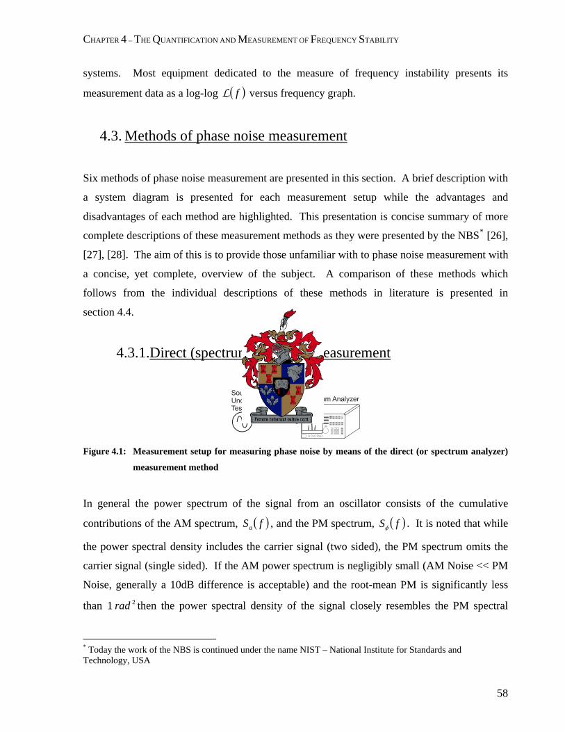
CHAPTER 4 – THE QUANTIFICATION AND MEASUREMENT OF FREQUENCY STABILITY
systems. Most equipment dedicated to the measure of frequency instability presents its
measurement data as a log-log ( )fL versus frequency graph.
4.3. Methods of phase noise measurement
Six methods of phase noise measurement are presented in this section. A brief description with
a system diagram is presented for each measurement setup while the advantages and
disadvantages of each method are highlighted. This presentation is concise summary of more
complete descriptions of these measurement methods as they were presented by the NBS* [26],
[27], [28]. The aim of this is to provide those unfamiliar with to phase noise measurement with
a concise, yet complete, overview of the subject. A comparison of these methods which
follows from the individual descriptions of these methods in literature is presented in
section 4.4.
4.3.1.Direct (spectrum analyzer) measurement
Figure 4.1: Measurement setup for measuring phase noise by means of the direct (or spectrum analyzer)
measurement method
In general the power spectrum of the signal from an oscillator consists of the cumulative
contributions of the AM spectrum, ( )fSa , and the PM spectrum, ( )fSφ . It is noted that while
the power spectral density includes the carrier signal (two sided), the PM spectrum omits the
carrier signal (single sided). If the AM power spectrum is negligibly small (AM Noise << PM
Noise, generally a 10dB difference is acceptable) and the root-mean PM is significantly less
than then the power spectral density of the signal closely resembles the PM spectral 21 rad
* Today the work of the NBS is continued under the name NIST – National Institute for Standards and Technology, USA
58

CHAPTER 4 – THE QUANTIFICATION AND MEASUREMENT OF FREQUENCY STABILITY
density in shape. Since amplitude limiting strips the signal of its AM spectrum in practical
oscillators and since most electrical oscillators easily meet the
requirement, the above two conditions are often simultaneously met in practice.
21 radPMmeanroot <<
Under these conditions the PM spectrum can be evaluated qualitatively by studying the power
spectrum of an oscillator on a spectrum analyser as is illustrated diagrammatically in the figure
4.1 above.
Advantages:
• The only measurement equipment required by this measurement method is a spectrum analyser – which is often available since it is used for so many other measurements.
• The setup and measurement is simple, straightforward and quick • No additional RO is required – actually the LO of the spectrum analyser acts as the
RO. Unfortunately this places a severe limitation on the best achievable sensitivity of this measurement method.
Disadvantages:
• The range of possible valid measurements is severely limited by the following characteristics of the specific spectrum analyzer employed for this measurement:
o dynamic range (typically from 10 dBm to -80 or -100 dBm) o resolution and video bandwidth (phase noise is usually expressed in on a per
hertz basis which requires very narrow filters) o LO phase noise
• Cannot measure close-in phase noise
Conclusion:
This method is best used to make quick qualitative judgements about the phase noise of
noisy sources.
59

CHAPTER 4 – THE QUANTIFICATION AND MEASUREMENT OF FREQUENCY STABILITY
4.3.2.Heterodyne (or beat frequency) measurement
Figure 4.2: Measurement setup for measuring phase noise by means of the heterodyne (or beat frequency)
measurement method
The method of heterodyne measurement can be explained at the hand of figure 4.2. The source under test (SUT) at frequency is mixed down to an intermediate frequency (IF) at frequency 1f
21 fff IF −= by use of a reference oscillator (RO) at frequency . From there the IF signal is then filtered through a low pass filter and amplified after which it is measured on either a period counter or a frequency counter at a constant rate. Since frequency counters generally have better resolution than period counters, frequency counters are the generally preferred choice. The normalized (or fractional) frequency fluctuation is then calculated from the measured IF signal [27], [28]:
0f
( ) ( ) ( )1
1
ftftfty iIFiIF
i−
= + (4.11)
From this, the Allan variance is calculated [27], [28]: 2yσ
( ) ( ) [∑ −
= + −−
=1
1
2
12
121 M
k kky yyM
τσ ] (4.12)
where M – number of data points iy – average normalized frequency fluctuation over time τ of the data
point
thi
By using tables or a computer the calculated values for can be translated to the single
sideband phase noise, , [27], [28].
2yσ
( )fL
60

CHAPTER 4 – THE QUANTIFICATION AND MEASUREMENT OF FREQUENCY STABILITY
Advantages:
• Particularly suitable for close-in phase noise measurements where the phase noise gradient is sharp with frequency, i.e. gradient of 3for 1 ≥ααf .
• No calibration is required. • Oscillators do not have to be phase locked.
Disadvantages:
• Not suitable for phase noise measurements at offsets far away from the carrier where the phase noise gradient is flat, i.e. gradient of 2for 1 ≤ααf .
• This measurement method is insensitive to spurious responses in the phase noise spectrum.
• Needs a RO whose phase noise is better than or alternatively the RO itself must be identical to the SUT. If the RO is not identical to the SUT, then the phase noise of the RO needs to be known in order to determine if it would make a suitable reference. This is done by comparing measurement results to the known phase noise of the RO. If the two are equal, it is possible that the phase noise of the SUT is lower than that of the RO and the RO can no longer be considered a valid reference.
Conclusion:
This method performs well for close-in phase noise measurements and can be employed to
measure all state-of-the-art oscillators – a characteristic lacking in many other phase noise
measurement techniques. If a suitable reference oscillator is not available an oscillator
identical to the SUT can be employed as a RO and it can be compensated for by subtracting
3 dB from the single sideband phase noise plot. This is a consequence of the property that
the measured phase noise has equal contributions of the phase noise of the RO and the
SUT. Finally, if determination of spurious responses in the phase noise is an essential aim
of the measurement an alternative measurement method is required.
61

CHAPTER 4 – THE QUANTIFICATION AND MEASUREMENT OF FREQUENCY STABILITY
4.3.3. Carrier removal measurement (also known as demodulation
methods)
4.3.3.1. Frequency demodulation (measurement with frequency
discriminator e.g. delay line with mixer, cavity, bridge types,
etc.)
Figure 4.3: Measurement setup for measuring phase noise by means of the frequency demodulation (or
frequency discriminator) measurement method
Figure 4.3 shows a diagrammatical representation of phase noise measurement through
frequency demodulation. The SUT signal is applied to a frequency discriminator (a device
which removes the carrier signal and translates the noise in the carrier sidebands to baseband).
After filtering and amplification, baseband analysis is performed on the signal by computer to
yield the single sideband phase noise spectral density, ( )fL . Although figure 4.3 shows how a
delay line and mixer can accomplish the frequency discrimination (which is the most common
way to establish the frequency discrimination) any frequency discriminator can be used. Other
examples of frequency discriminators that have been used in such a phase noise measurement
setup are cavity and bridge type discriminators.
62

CHAPTER 4 – THE QUANTIFICATION AND MEASUREMENT OF FREQUENCY STABILITY
Advantages:
• This provides a suitable method for measuring the phase noise of sources that display large phase deviations at low rates of change – e.g. free running VCOs.
• Requires no RO or phase locked loop (PLL).
Disadvantages:
• Calibration requires a significant shift in the output frequency of the SUT. (This can easily be accomplished by VCOs.)
• If a delay line is used, its narrow bandwidth characteristics normally require that a delay line be manufactured specifically at the frequency of the SUT.
• The length (in multiples of the SUT period) of the delay line is critical and must be carefully chosen. Longer lines provide better demodulation sensitivity while shorter lines yield a phase noise spectral density graph over a wider frequency range.
• Since this is a baseband detection system, system sensitivity degrades as f1 as the
phase noise is evaluated closer to the carrier.
Conclusion:
This method is often used to measure the phase noise of free running VCOs as many other
techniques require phase locking (with a very small loop bandwidth) with a reference
source which can often not follow the phase of a free running VCO fast enough to maintain
a lock. Such measurements usually require no close-in phase noise data. Since this is the
only method of phase noise measurement that does not require a reference source it is often
referred to as the one-oscillator technique.
63

CHAPTER 4 – THE QUANTIFICATION AND MEASUREMENT OF FREQUENCY STABILITY
4.3.3.2. Phase demodulation (measurement with phase
detectors)
Figure 4.4: Measurement method for measuring phase noise by means of the phase demodulation (or
phase detector) measurement method
Figure 4.4 shows a diagram of the system required to do phase noise measurements through
phase demodulation. A mixer can be employed as a linear phase detector only if it is driven by
two sources that are exactly in quadrature (90° phase difference). This quadrature condition is
met by phase locking the RO (which needs to be frequency controllable) to the SUT. The
signal at the output of the mixer is then fed through a low pass filter and amplified before a
baseband analysis is performed by computer. The result is the single sideband phase noise,
. The measured single sideband (SSB) phase noise is the combined SSB phase noise of
both oscillators.
( )fL
64

CHAPTER 4 – THE QUANTIFICATION AND MEASUREMENT OF FREQUENCY STABILITY
Advantages:
• Since the carrier signal is suppressed and a log-log analysis can be performed a wide dynamic range can be achieved on both axis:
o 0 – 170 dBc/Hz on the phase noise axis o 0.01Hz – 10MHz on the frequency axis
• Close-in phase noise measurements can be performed. • Spurious phase signals are accurately detected and can easily be distinguished in the
phase noise sideband as sharp peaks standing out far above the immediately surrounding phase noise.
• The PLL ensures that this method is insensitive to long term frequency drift between the SUT and the RO.
• The same computer that is used to perform baseband analysis can be used to automate measurements. This makes this method speedy and precise in calibration and quick and easy to measure at many frequency points sequentially.
Disadvantages:
• A RO with significantly lower phase noise than the SUT is required. It is important that the phase noise of the RO is known as to be sure when measurement data is evaluated that the measured phase noise can indeed be ascribed to the SUT and not to the RO. It is however possible to make accurate phase noise measurements using a RO whose phase noise is unknown and not necessarily better than the SUT – but only if the SUT and the RO are identical.
• Control of the PLL must be precise as disturbances in the quadrature condition will affect the linearity of the phase detector (mixer). Furthermore the presence of the PLL affects the measurements and this must be compensated for in data processing. This compensation becomes increasingly important as the phase noise is evaluated closer to the carrier (as the frequency at which the phase noise is evaluated approaches the loop bandwidth). If the offset frequency at which the phase noise is evaluated is less than the loop bandwidth the system can no longer be considered a phase demodulation system – in such a case it is a frequency demodulation system. The computer performing the baseband analysis may be programmed to seamlessly perform frequency demodulation instead of phase demodulation under such conditions so that the user simply sees the result: the single sideband phase noise relative to the carrier, ( )fL .
Conclusion:
This was the chosen method of phase noise measurement for this project – initially because
of the availability of measurement equipment. It was however also the method best suited
to this project as it yields the best overall sensitivity away from the carrier (at modulation
frequencies larger than the PLL bandwidth) – which was required by some extremely low
65

CHAPTER 4 – THE QUANTIFICATION AND MEASUREMENT OF FREQUENCY STABILITY
phase noise measurements that were done. The operation of a mixer as a phase detector is
considered more carefully in appendix A.
This method is best suited to measure the phase noise of phase stable sources (e.g. crystal
oscillators, PLL that is locked to a phase stable reference and low noise frequency
synthesizers) over a large modulation frequency range. The result is a phase noise
measurement system that can measure the phase noise both far away from and close to the
carrier in a single, convenient measurement setup.
4.3.4.Time difference method
Figure 4.5: Measurement of phase noise by means of the time difference measurement method
In figure 4.5 a diagram of the measurement setup to measure phase noise by means of the time
difference method is given. A time interval counter (a device which measures the time
difference between positive zero crossings of two sinusoidal input signals) is employed to
measure the time difference between a phase stable RO and the SUT.
Time interval counters often do not have the necessary resolution to measure precisely enough
for phase noise measurements. In order to increase the resolution with which the time
difference between positive zero crossings of the two signals is measured, the periods of the
measured signals are slowed down in time by inserting identical frequency dividers between
the sources and the time interval counter. When this is done care should be taken with such
frequency dividers as they have been known to contribute (sometimes dominantly) to the
measured phase noise.
66

CHAPTER 4 – THE QUANTIFICATION AND MEASUREMENT OF FREQUENCY STABILITY
Advantages:
• Simple measurement setup. • No calibration required. • Time domain measurements can be translated to frequency domain parameters. Disadvantages:
• Phase noise contribution of frequency dividers needs to be known and compensated for.
• RO that is more phase stable than the SUT is required alternatively a RO identical to the SUT may be used – but must be compensated for in measurement results.
Conclusion:
If a time interval counter happens to be available this is an easy and convenient method of
measuring phase noise. Often a good frequency synthesizer that is known to have low
phase noise can be employed as a RO at the required frequency. If frequency dividers are
not available, they should be designed for low phase noise contribution as first priority.
How the time interval as measured by the time interval counter can be related to frequency
stability parameters is considered in more detail in the dual mixer time difference method
that follows below. Although the parameter expressions (equations 4.13 through 4.17)
deduced in the next section are not identical and thus cannot be applied directly to the
method discussed here, it should provide sufficient insight to deduce the required
expressions easily. This does not bind this method of measurement to the disadvantages of
the subsequent method.
67

CHAPTER 4 – THE QUANTIFICATION AND MEASUREMENT OF FREQUENCY STABILITY
4.3.5.Dual mixer time difference (DMTD) method
Figure 4.6: Measurement of phase noise by means of the dual mixer time difference method
The discussion of the dual mixer time difference (DMTD) method is represented by figure 4.6.
The output signal of the SUT oscillates at a frequency, , while the output signal of the RO
oscillates at a frequency, .
1f
2f
Two conditions need to be met in order for this measurement method to yield useful results:
Condition 1:
A RO at the same frequency as the SUT ( ) is required. 21 ff =
This condition requires that the SUT and the RO are at the same frequency in the long term
frequency stability sense so that the short term frequency instabilities are tolerable.
Both the signals of the SUT and RO are then separately mixed down to an IF through
application of a mutual local oscillator (LO) (which oscillates at a frequency, ) to both 0f
68

CHAPTER 4 – THE QUANTIFICATION AND MEASUREMENT OF FREQUENCY STABILITY
mixers. After low pass filtering and amplification the down mixed SUT and RO signals (at
frequencies 01 ff − and 02 ff − respectively) are fed to a time interval counter.
Condition 2:
By using an adjustable phase shifter, the phase of the SUT may be adjusted so that the zero
crossings of the signals entering the time interval counter coincide.
This condition relies heavily on the first condition. If the frequencies of the RO and the SUT
are not identical, the matching zero crossings will tend to move progressively further apart over
time.
If both conditions are met, the phase noise contribution of the LO cancels (for certain types of
noise) so that the noise contribution of the LO may then be neglected in measurements.
The time interval counter then measures the time between positive zero crossings of the two
beat signals. This is equivalent to measuring the time difference between the zero crossings of
the SUT and the RO – but where the resolution of the time interval counter has been amplified
by the ratio:
01
1
fffATIC −
= (4.13)
If one assumes that the LO operates at a lower frequency than the SUT so that
001 >− ff (4.14)
and also that the positive zero crossing of the beat signal from the SUT initiates the timer and
the positive zero crossing of the beat signal from the RO stops the timer then equations can be
deduced for the time difference, ( )ix , and the normalized (or fractional) frequency fluctuation
of the SUT relative to the RO, ( )2, ,τiy ROSUT .
69

CHAPTER 4 – THE QUANTIFICATION AND MEASUREMENT OF FREQUENCY STABILITY
From the time interval counter reading for the measurement thi ( )itΔ , the time difference, ( )ix ,
can be calculated:
( ) ( )fk
ffitix
b
+−Δ
=πφ
τ 2 (4.15)
where – time interval counter measurement ( )itΔ thi bτ – period of the beat signals (condition 1 guarantees their equality) – the carrier frequency of the SUT ( from condition 1) f 21 fff == φ – the phase delay contributed by the adjustable phase shifter – an integer to keep track of the time difference ascribed to complete k
cycle differences between the SUT and the RO. For frequency stability measurements the relative time difference is more important than the absolute time difference so that 0=k can often be assumed unless the phase accumulation exceeds one cycle (typically if measurements are done over a very long time or if very phase unstable sources are measured).
The normalized (or fractional) frequency fluctuation of the SUT relative to the RO can also be
calculated:
( ) ( ) ( )
( ) ( )
( ) ( )f
itit
ixixf
ififiy
b
ROSUT
2
21,
1
1
,,,
τ
τ
τττ
Δ−+Δ=
−+=
−=
(4.16)
where τ – time between time interval counter measurements – instantaneous frequency of SUT when measurement was taken ( τ,1 if )
)thi
– instantaneous frequency of RO when measurement was taken ( τ,2 if thi – the carrier frequency of the SUT ( from condition 1) f 21 fff == – time interval counter measurement ( )itΔ thi bτ – period of the beat signals (condition 1 guarantees their equality)
From equations 4.15 or 4.16 the Allan variance, , can be calculated and from there formulae
from tables
2yσ
* can be used to program computers to calculate the SSB phase noise, ( )fL .
* Table 1, p 18, [26] alternatively Table 11.1, p 36, [27]
70
CHAPTER 4 – THE QUANTIFICATION AND MEASUREMENT OF FREQUENCY STABILITY
Furthermore, averaging of the normalized (or fractional) frequency fluctuation over a positive
integer multiple, , of m bτ amounts to:
( ) ( ) ( )b
bROSUT mixmixmiy
ττ −+
=,, (4.17)
Advantages:
• Make very high resolution time domain measurements. • Good value for money. Required components are not very expensive. • No phase locked loop required.
Disadvantages:
• Since condition 1 requires that the frequencies of the SUT and RO have to be exactly the same (in the long term frequency stability sense) this measurement setup is only really applicable to oscillators that employ atomic standard resonators i.e. cesium, rubidium and hydrogen frequency standards. Even quartz crystal resonators cannot be made to resonate at exactly the same frequency – albeit very close.
• A reference oscillator is required.
Conclusion:
By introducing a third oscillator the DMTD method yields an improvement of about two
orders of magnitude in precision over other time domain measurement systems like the
standard time difference method discussed earlier. It is however suitable only to the
measurement of identical frequency sources like atomic standard oscillators as the SUT and
the RO, by necessity, have to operate at exactly the same frequency.
71
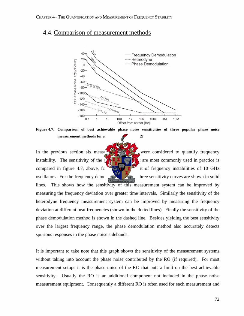
CHAPTER 4 – THE QUANTIFICATION AND MEASUREMENT OF FREQUENCY STABILITY
4.4. Comparison of measurement methods
Figure 4.7: Comparison of best achievable phase noise sensitivities of three popular phase noise
measurement methods for a 10 GHz oscillator [12]
In the previous section six measurement methods were considered to quantify frequency
instability. The sensitivity of the three methods that are most commonly used in practice is
compared in figure 4.7, above, for the measurement of frequency instabilities of 10 GHz
oscillators. For the frequency demodulation method three sensitivity curves are shown in solid
lines. This shows how the sensitivity of this measurement system can be improved by
measuring the frequency deviation over greater time intervals. Similarly the sensitivity of the
heterodyne frequency measurement system can be improved by measuring the frequency
deviation at different beat frequencies (shown in the dotted lines). Finally the sensitivity of the
phase demodulation method is shown in the dashed line. Besides yielding the best sensitivity
over the largest frequency range, the phase demodulation method also accurately detects
spurious responses in the phase noise sidebands.
It is important to take note that this graph shows the sensitivity of the measurement systems
without taking into account the phase noise contributed by the RO (if required). For most
measurement setups it is the phase noise of the RO that puts a limit on the best achievable
sensitivity. Usually the RO is an additional component not included in the phase noise
measurement equipment. Consequently a different RO is often used for each measurement and
72
CHAPTER 4 – THE QUANTIFICATION AND MEASUREMENT OF FREQUENCY STABILITY
so it makes sense to specify the sensitivity of the system without taking that of the RO into
account.
The most essential aspects of all six frequency instability measurement methods can be
compared in a table. Such a comparison is found in table 4.1 (attributes marked as "--" indicate
uncertainty due to incomplete available information). This is a tabular summary made by the
author of this thesis from descriptions of the measurement methods involved as presented in
[26], [27] and [28]. Table 4.1: Comparison of six methods of frequency instability measurement
Spec
trum
Ana
lyse
r M
easu
rem
ent
Het
erod
yne
Mea
sure
men
t
Freq
uenc
y D
emod
ulat
ion
Phas
e D
emod
ulat
ion
Tim
e D
iffer
ence
Dua
l Mix
er T
ime
Diff
eren
ce (D
MTD
)
RO Required No Yes No Yes Yes Yes
PLL Required* No No Some
methods Yes No No
Very sharp filters required
Yes No No No No No
Sensitivity Poor Excellent Poor Excellent Moderate Excellent
Range Excellent Close to carrier
Far away from carrier
Excellent -- --
Calibrate No No Yes Yes No No Automation Some Some Some Complete Some Some Sensitive to frequency drift
Yes Yes No No Yes Yes
Detects spurious signals
Yes No Yes Yes No No
* The presence of a PLL requires the RO to be frequency selectable by means of a control voltage to the oscillator (VCO)
73

CHAPTER 4 – THE QUANTIFICATION AND MEASUREMENT OF FREQUENCY STABILITY
4.5. What measurement method was used for this project and why?
Figure 4.8: Photograph of the Aeroflex PN900B Phase Noise Measurement System
The method of phase demodulation was the measurement method employed in this project.
Initially it was chosen solely because such measurement equipment was available to the author
in the form of the Aeroflex PN9000B Phase Noise Measurement System that can be seen in the
photograph above. Later, after careful consideration of the various measurement techniques
available for the measurement of phase noise, it was concluded that not only was the Aeroflex
PN9000B Phase Noise Measurement System sufficient, but it was also the technique best suited
to the measurement of low phase noise crystal oscillators. Not shown in the photograph above
is the personal computer (PC) responsible for the automation of measurements and the
processing of measurement data that is part of the measurement system.
74

CHAPTER 4 – THE QUANTIFICATION AND MEASUREMENT OF FREQUENCY STABILITY
What made this measurement system so suitable for these measurements were:
• The excellent sensitivity of the measurement equipment. • The wide range of offset frequencies over which the phase noise could be measured.
Close-in phase noise measurements (from 0.01 Hz) could be made as well as phase noise measurements at offset frequencies far away from the carrier (up to 10 MHz away).
• Spurious responses in the phase noise spectrum are accurately detected. • The equipment made provision for either using the low phase noise RO that is built
into the measurement system or for using a custom RO in the case where the phase noise of the built-in RO is insufficiently high. Both these options were used extensively for this project.
• The measurement system can measure phase noise on any oscillator whose phase noise needs to be evaluated around a carrier frequency that falls in the range 5 MHz to 18GHz.
• Measurements are automatically repeated many times and averaged to reduce the measurement uncertainty.
In addition to the necessary features that are mentioned above, the measurement system also
had many other features that made it convenient to use. Such features include:
• Calibration is highly automated, very accurate and is performed speedily. • A PLL is included and monitored by the PC. As the accuracy of the measurements
depend heavily on the quadrature condition enforced by the PLL, it is important to know when the loop control is insufficient. The PC provides warnings in case any danger of such inaccurate measurements exists.
• The measurement system is highly automated and thousands of measurements are performed and processed sequentially and seamlessly so that the user is presented only with the measurement results. Such a sequence of measurements, if the offset frequency at which the phase noise is measured spans from 1 Hz to 100 kHz, takes about 20 minutes.
• The PC presents to the user a graph of the single sideband phase noise relative to the carrier, ( )fL , so that the need for further data processing is eliminated.
4.6. Measurement procedure
The measurements that were done for this project can be divided into two categories:
measurements done on moderate phase noise oscillators and measurements done on low phase
noise oscillators.
75

CHAPTER 4 – THE QUANTIFICATION AND MEASUREMENT OF FREQUENCY STABILITY
One of the oscillator parameters that can be changed to improve the phase noise of an oscillator
is the loaded quality factor, , of the resonator. AT-cut quartz crystal resonators have an
unloaded quality factor in the order of 100 000 in oscillators while specially designed SC-cut
quartz crystal resonators had an unloaded quality factor exceeding 1 200 000 in oscillators.
LQ
When the AT-cut crystals were used, the RO that was part of the Aeroflex PN9000B Phase
Noise Measurement System had sufficiently better phase noise than the SUT to yield accurate
phase noise measurements. However, when the SC-cut crystals were used in the SUT, the
problem arose that the RO that was part of the Aeroflex PN9000B Phase Noise Measurement
System no longer yielded low enough phase noise to be considered a reliable reference. To
overcome this problem, oscillators were built in identical pairs and measured in pairs. One
acted as the RO and the other as the SUT.
In this fashion the cumulative contribution of phase noise from both the SUT and the RO was
measured. Since these oscillators were identical, it is fair to assume that each one contributed
to the cumulative phase noise measurement equally. In order to find the phase noise
contribution of the SUT only half the measured phase noise is taken – the Aeroflex PN9000B
Phase Noise Measurement System does not make this correction automatically. Consequently
it is important to remember to subtract 3 dB from the SSB phase noise relative to the
carrier, , over the entire offset frequency range. That is why the distinction is made
between measurements done on moderate phase noise oscillators and measurements done on
low phase noise oscillators.
( )fL
76

CHAPTER 4 – THE QUANTIFICATION AND MEASUREMENT OF FREQUENCY STABILITY
4.6.1.Measurement on moderate phase noise oscillators
Figure 4.9: Moderate phase noise oscillator measurement setup:
(a) Measurement setup for the phase noise measurement of a moderate phase noise SUT on the Aeroflex PN9000B phase noise measurement system
(b) System diagram for the measurement of phase noise of a moderate phase noise SUT on the Aeroflex PN9000B phase noise measurement system.
Figure 4.9 shows the measurement setup to measure the phase noise of a SUT if the phase
noise of the SUT is moderate. For the purpose of this explanation, a source with moderate
77

CHAPTER 4 – THE QUANTIFICATION AND MEASUREMENT OF FREQUENCY STABILITY
phase noise is such that its phase noise exceeds the phase noise of the Aeroflex PN9100 RF
Synthesizer (which is part of the Aeroflex PN9000B Phase Noise Measurement System) by at
least 3 dBc/Hz over the entire offset frequency range of interest. Specifically, according to the
documentation of the Aeroflex PN9000B Phase Noise Measurement System, this restricts the
phase noise of a 10 MHz SUT to be 3 dBc/Hz in excess of: -96 dBc/Hz at an offset frequency
of 1 Hz from the carrier, -126 dBc/Hz at an offset frequency of 10 Hz, -141 dBc/Hz at 100 Hz
offset frequency and -155 dBc/Hz from 1kHz and greater offset frequencies. The phase noise
of the Aeroflex PN9100 RF Synthesizer at 10MHz is plotted in the solid line graph in figure
4.10 below. From consideration of figure 4.10, a moderate phase noise SUT is defined as a
source for which the phase noise is above the dashed line over the frequency range of interest.
100 101 102 103 104 105-160
-140
-120
-100
-80
-60
-40
-20
0
Offset frequency from carrier [Hz]
Sin
gle
side
band
pha
se n
oise
rela
tive
to th
e ca
rrier
, L(f)
[dB
c/H
z]
Phase noise of the PN9100 RF Syntesizer reference at 10MHz
PN9100 RF SynthesizerLower limit of SUT
Figure 4.10: Phase noise of the PN9100 RF Synthesizer reference oscillator at 10 MHz
The following discussion may be followed with frequent reference to figure 4.9 (a). The PC is
permanently connected to the Aeroflex PN9000B Phase Noise Measurement System. Another
permanent connection can be seen to the far right of figure 4.9 (a) where the 10 MHz Out-port
is connected to the 10 MHz In-port on the Down Converter Time Base module.
In order to perform a measurement on a moderate phase noise SUT the Aeroflex PN9100 RF
Synthesizer (that is part of the measurement system) is used as the reference source. This may
78

CHAPTER 4 – THE QUANTIFICATION AND MEASUREMENT OF FREQUENCY STABILITY
be done by connecting the output-port of the RF Synthesizer module to the LO Input-port of the
Phase Detector module and also connecting the Tune Control Out-port on the Lock Control
module to the Tune Input-port on the RF Synthesizer module. Finally the SUT is connected to
the RF Input port of the Phase detector module.
Without much detailed discussion, figure 4.9(b) shows a system diagram of the measurement
setup of figure 4.9(b) in order to improve one’s understanding of the measurement setup. In
this figure dotted line boxes emphasize which parts of the setup are contained inside the
Aeroflex PN9000B Phase Noise Measurement System and which parts of the setup constitute
the PLL.
When the necessary connections have been made, as discussed in the previous two paragraphs,
software on the PC is used to calibrate, set up and automate a sequence of phase noise
measurements. As these measurements are made, the computer plots the phase noise data
graphically against offset frequency.
79

CHAPTER 4 – THE QUANTIFICATION AND MEASUREMENT OF FREQUENCY STABILITY
4.6.2.Measurement on low phase noise oscillators
Figure 4.11: Low phase noise oscillator measurement setup:
(a) Measurement setup for the phase noise measurement of a low phase noise SUT on the Aeroflex PN9000B Phase Noise Measurement System.
(b) System diagram for the measurement of phase noise of a low phase noise SUT on the Aeroflex PN9000B phase noise measurement system
For the purpose of this project a low phase noise SUT is a source which does not comply with
the restriction described in the first paragraph of the previous section, section 4.6.1. When
measuring such a source, the phase noise of the SUT will be better than the phase noise of the
Aeroflex PN9100 RF Synthesizer (which is integrated into the measurement system) so that this
80

CHAPTER 4 – THE QUANTIFICATION AND MEASUREMENT OF FREQUENCY STABILITY
integrated RO can no longer be considered a valid reference. As has been stated earlier, this
problem was overcome by building identical pairs of the SUT and then using one as a RO.
Two further challenges arose in this solution to the problem of constructing a better reference
than the Aeroflex PN9100 RF Synthesizer. The first problem was that – for the phase
demodulation measurement method – the RO is required to be frequency selectable i.e. the RO
has to be a voltage controlled oscillator (VCO). What made this problem especially hard to
overcome was that it was practically difficult to change the oscillation frequency of an
oscillator with such a high quality factor resonator. Prof. P.W. Van Der Walt suggested that a
series resonant LC network could be employed to accomplish this. Through the use of a
varactor diode such a series resonant network was designed and implemented to change the
frequency of oscillation over a 2.8 Hz range around 10 MHz with a control voltage that ranged
between 0 – 20 V. Practically it was found that this 2.8 Hz tuneable range was sufficient to
keep such a RO locked in phase quadrature with respect to its identical SUT counterpart.
The second problem was that the SC-cut crystal resonators were extremely sensitive to changes
in temperature. This was overcome by designing a temperature controller to keep the
resonators at their respective turnover point temperature (often simply abbreviated as TO). For
quartz crystal resonators the resonant frequency’s sensitivity to changes in temperature reaches
a minimum at the TO. Practically it was found that (even with the temperature controllers
installed) very slight movements of air in the room where the measurements were done caused
frequency drift of the oscillators to the point where a phase locked loop was possible to
establish – but hard to maintain long enough to complete a set of measurements (which
typically took about 20 minutes). This further challenge was overcome by containing the entire
oscillator, with its resonator and its temperature controller in an enclosed aluminium box.
The frequency-temperature dependence of the quartz crystal resonators also allowed for the
frequencies of the SUT and RO to be brought to close approximation of each other by simply
adjusting the temperature controller of one of the oscillators a little. Thus the fundamental
frequency of oscillation of both oscillators could be brought so close to each other that the 2.8
81

CHAPTER 4 – THE QUANTIFICATION AND MEASUREMENT OF FREQUENCY STABILITY
Hz tuneable frequency range of the RO provided sufficient compensation to sustain the phase
locked loop.
The design of the temperature controller that was used for such measurements is presented in
appendix B while appendix C shows how one of the two quartz crystal resonators was made
frequency selectable.
Figure 4.11 shows the measurement setup for phase noise measurements on a low phase noise
SUT. Figure 4.11 (a) shows the connections made to the Aeroflex PN9000B Phase Noise
Measurement System. Apart from the exception that the RF Synthesizer module of the
measurement system is now replaced by a custom designed VCO, this measurement setup is
identical to that shown in figure 4.9(a). Figure 4.11(b) shows a system diagram of the
measurement setup of figure 4.11(a). Again the dotted line boxes emphasize which parts of the
setup are contained inside the Aeroflex PN9000B Phase Noise Measurement System and which
parts of the setup constitute the PLL. From this it can be noted that the RO is no longer inside
the Aeroflex PN9000B Phase Noise Measurement System (as it was custom designed).
4.7. Conclusion
A thorough theory of the quantification and measurement of frequency stability (or rather
frequency instability) is available and was presented concisely. It was also shown how
frequency instability measurements taken by different measurement methods can be compared
with each other if it is expressed in terms of the single sideband phase noise relative to the
carrier, . Independent of which physical parameter was measured by the phase noise
measurement method employed, it was shown how the SSB phase noise relative to the carrier,
( )fL
( )fL , may be found. Finally attention was given to the specific measurement method applied
in this project – phase noise measurement through phase demodulation. For this measurement
method, consideration was given to exact measurement setups through highlighting different
problems encountered together with the solutions by which they were overcome.
82

Chapter 5
Design of a low phase noise crystal oscillator
In his article M.M. Driscoll highlights the following factors as design goals that are to be
achieved simultaneously in an oscillator when designing crystal oscillators for low phase noise
[17]:
• Achieving the best ultimate signal-to-noise ratio possible. This statement is equivalent
to: reducing the ultimate (far away from the carrier) phase noise to a minimum.
• Maximising the loaded quality factor of the resonator, . LQ
• Suppression of f1 flicker of phase type noise (which is caused by the amplifier).
The expression for the ultimate signal-to-noise ratio was presented in chapter 2 as a
consequence of Leeson’s phase noise model in equations 2.17 and 2.18. These equations show
that the ultimate phase noise can be improved by reducing the effective noise figure of the
oscillator, , and also by increasing the power at the input to the sustaining stage of the
oscillator, . The input to the sustaining stage of the oscillator may be improved by
increasing the signal level at the output of the oscillator since these are directly related by the
gain of the sustaining stage. The power cannot be increased indefinitely however. Crystal
resonators have a limit on how much power they can safely dissipate before destruction. For
AT-cut quartz crystals maximum dissipated power is limited to 1 mW while for SC-cut crystal
resonators this limit comes to 5 mW. Driscoll also points out that when the crystal resonator is
employed at its series resonant frequency an improvement in the ultimate noise floor is
observed over when it is employed away from its series resonant point [17].
F
inP
The insight that maximising the loaded quality factor, , follows directly from Leeson’s
equation which was presented in chapter 2 as equation 2.16. In order to design a circuit that
yields a high loaded quality factor, , from a quartz crystal resonator the oscillator circuit has
LQ
LQ
83

CHAPTER 5 – DESIGN OF A LOW PHASE NOISE CRYSTAL OSCILLATOR
to present minimal load impedance in series with the crystal resonator at the oscillation
frequency [17]. Driscoll’s oscillator achieves this by employing the crystal resonator between
the emitter and ground of a common-emitter bipolar junction transistor (BJT) amplifier [17].
In this way the equivalent series load presented to the resonator is the input-impedance to the
amplifier divided with the current gain factor, β . In this way the series load presented to the
crystal resonator can be made to be less than 5% of the series resistance of the crystal resonator
yielding a loaded-to-unloaded quality factor ratio as high as 95 %.
Leeson’s phase noise model (which was presented in section 2.4.1) relied on linear time-
invariant (LTI) assumptions [13]. As all electrical oscillators display non-linear behaviour
Leeson’s phase noise model can be expected to fall short in its application to phase noise
prediction.
Recall from the discussion of mechanisms of phase noise in section 2.3 that f1 flicker of
phase type noise is caused by noise added to the carrier by frequency multiplication action
while noise added to the carrier by simple addition mechanisms does not contribute to phase
noise around the carrier but only to the ultimate noise floor. This has been observed to occur in
transistors. With this insight it becomes clear that f1 flicker of phase type noise from the
transistor(s) can be limited by minimising the cause of frequency multiplication action in an
oscillator. Frequency multiplication action is caused in all oscillators by the inherently
necessary non-linear signal limiting behaviour. Another way to minimise f1 flicker of phase
type noise is to choose a transistor with a low f1 flicker noise crossover point. In general
BJT transistors have low f1 flicker noise crossover points compared to other transistor
technologies.
If however the non-linear behaviour in an oscillator can be restricted within a sub-circuit of that
oscillator it can be expected that Leeson’s equation would under predict the phase noise of the
oscillator with an error dependent on the phase noise contribution of that sub-circuit. In his
84
CHAPTER 5 – DESIGN OF A LOW PHASE NOISE CRYSTAL OSCILLATOR
article Driscoll suggests exactly such a strategy where the non-linear behaviour of his oscillator
be limited to occur within a sub-circuit known to contribute minimal phase noise and disturb
the loaded quality factor of the resonator minimally [17]. The result is that Leeson’s model
would predict the phase noise of the oscillator with a negligible error*. While Driscoll only
considers this non-linear signal limiting stage as realised by a second common-base transistor,
he suggests two other methods of achieving this: an auxiliary low-noise automatic gain control
(AGC) circuit or two back-to-back Schottky barrier diodes known for their low-phase noise
contribution [17]. A further advantage of this strategy is that the part of the oscillator circuit
which is free from non-linear behaviour is then designed for linear class A amplifier operation
– which is expected to yield optimal phase noise performance [17].
For the Driscoll oscillator that was designed for this project this non-linear signal limiting was
achieved through a single Schottky barrier diode with its biasing network. The circuit diagram
is presented in figure 5.1 and the design of this circuit follows.
* It may be noted that because Leeson’s phase noise model is based on linear assumptions it would under-predict the phase noise. Non-linear behaviour in oscillators cause an increase in phase noise rather than a decrease in phase noise due to the frequency multiplication action associated with this behaviour (see section 2.3). The immediate consequence is that if an oscillator can be designed to behave as close as possible to a linear system its phase noise would accordingly be reduced while simultaneously its measured phase noise would follow closely its phase noise as predicted by Leeson’s model. The low phase noise results of Driscoll’s publication bears testimony to this [17].
85

CHAPTER 5 – DESIGN OF A LOW PHASE NOISE CRYSTAL OSCILLATOR
Vout (into 50 Ω)
R3
R2
Gnd
Gnd
GndGnd
R5Q2
X1
R12.7 kΩ
470 Ω
82 Ω
1.2 kΩ
R6300 Ω (330//3k3)
R7
1 kΩ
C4
C2
10 nF
L1130 μH
C1
Q12N2222
2N2222
R4
C3
C6 C8C7
100 nF
10 nF
47 μF10 nF
100 pF
C51.8 kΩBAT54
(6.49 nH)
VCC (15 VDC)
VCC (15 VDC)
T50-2 coreT1
7.24 nHL2
D1
5-65 pF(23-55 pF)
155-215 pF
11:3
Figure 5.1: Driscoll oscillator circuit where non-linear limiting is restricted to a single active element – i.e.
a Schottky barrier diode, D1
5.1. Design of a Driscoll oscillator
The operation of the Driscoll oscillator circuit which is presented in figure 5.1 may briefly be
described. Oscillation is sustained by strictly linear class A amplifier operation effected by the
cascade transistor combination of the common-emitter transistor Q1 and the common-base
transistor Q2 and the biasing networks for these transistors. Furthermore the oscillator is
designed to operate at the series resonant point of the crystal X1. At this frequency the crystal
may be simply modelled by its equivalent series resistance of 80 Ω. The inherent resonant
point of the oscillator (without consideration of the crystal) is determined by the parallel
resonant point of the capacitance C3 and primary inductance of T1. The effect of the crystal
may be removed by replacing the crystal and its frequency adjusting sub-circuit (i.e. X1, L2
and C1 in figure 5.1) by a resistor of 80 Ω. This allows for setting the inherent resonant point
of the oscillation independently of the crystal resonator by adjusting the capacitance C3 until
oscillation is observed at the resonant frequency of the crystal. Such adjustment ensures
86

CHAPTER 5 – DESIGN OF A LOW PHASE NOISE CRYSTAL OSCILLATOR
operation of the crystal at its series resonant point when it and its frequency adjusting sub-
circuit is inserted back into the circuit. Apart from determining the inherent resonant point of
the oscillator, the transformer T1 also ensures positive feedback from the output back to the
input of the cascade amplifier combination at slightly more than unity gain. In order to
maintain linear class A operation by the cascade amplifier combination non-linear signal
limiting outside of this amplifier is required somewhere in the feedback path. This requirement
is satisfied by the Schottky barrier diode D1 and its supporting passive components R6, R7 and
C6. The capacitors C7 and C8 acts as bypassing capacitors for the oscillator while the
capacitor C5 establishes impedance matching at the output of the oscillator.
The oscillator was designed to yield 15 dBm output power at 10 MHz into a 50 Ω load. For
optimum phase noise performance as much power as possible needs to be dissipated in the
crystal resonator. However in order to avoid destruction of the resonator the power dissipated
in the crystal resonator should be limited to a maximum of 5 mW. From this constraint the
peak small-signal emitter current for transistor Q1 may be calculated:
mA11mA12.1180005.022
)()( ≈=⋅=⋅=
XtalS
Xtalpeakc R
Pi (5.1)
The quiescent DC collector current for both transistors is taken to be about twice the small-
signal emitter current for transistor Q1:
(5.2) mA20=CQI The emitter-voltage of Q1 is accepted to be:
(5.3) VV QE 5.1)1( = To ensure linear operation of Q1 the collector-voltage of Q1 is accepted to be:
(5.4) VV QE 5)2( = The cascade amplifier combination is expected to drive a 600 Ω load at the collector of
transistor Q2:
87

CHAPTER 5 – DESIGN OF A LOW PHASE NOISE CRYSTAL OSCILLATOR
Ω≈ 600loadZ (5.5) This load impedance of 600 Ω is then matched to 50 Ω by the capacitance C5 at the frequency
of oscillation. Such a high load impedance ensures sufficient positive feedback to be
established by T1 which itself is expected to provide a relatively small impedance of 60 Ω at
the collector of Q2 at the oscillation frequency:
Ω≈ 60)(1 primaryTZ (5.6) From the requirements set out in equations 5.1 through 5.6 the biasing networks for transistors
Q1 and Q2 may be designed.
Choosing the bias current through resistors R1 and R2 to be 5 mA and application of
elementary circuit analysis yield:
( ) ( )
Ω≈Ω=−−
=−−
= kkI
VVVCCR
R
onBEQE 7.256.2005.0
7.05.11511
)()1( (5.7)
( ) ( )
Ω≈Ω=+
=+
= 470440005.0
7.05.122
)()1(
R
onBEQE
IVV
R (5.8)
The value of resistor R3 may be found from equations 5.2 and 5.3:
( ) Ω≈=== 8275020.05.13 1
CQ
QE
IV
R (5.9)
Similarly choosing the bias current through resistors R4 and R5 to be 5 mA together with
elementary circuit analysis and equation 5.4 yield:
( ) ( )
Ω≈=−−
=−−
= k8.11860005.0
7.051544
)()2(
R
onBEQE
IVVVCC
R (5.10)
( )Ω≈Ω=
+=
+= k2.1k1140
005.07.055
5
)()2(
R
onBEQE
IVV
R (5.11)
The inductance of the primary winding of transformer T1 follows from equation 5.6:
88

CHAPTER 5 – DESIGN OF A LOW PHASE NOISE CRYSTAL OSCILLATOR
nH95510102
602 6
0
)(1)(1 =
×⋅⋅=
⋅⋅=
ππ fZ
L primaryTprimaryT (5.12)
L2L1
|Zpr
imar
y su
b-ci
rcui
t|=
600
Ω
|Zsecondary sub-circuit |
= 400 Ω
n:1T1
Figure 5.2: An equivalent circuit from the perspective of the transformer T1 where the sub-circuits
connected to the primary and secondary windings have been reduced to equivalent impedances.
The ratio of the windings of the transformer T1 may be found from the equivalent circuit which
is presented in figure 5.2. Firstly it is noted that the small signal gain from the secondary
winding of the transformer towards its primary winding in the oscillator of figure 5.1 is
dominated by the ratio:
5.780600~
)(
=≈XtalS
loadv R
ZA (5.13)
Consequently if the transformer ratio is exactly equal to 1:vAn = then the oscillator’s output
signal would be fed back at an attenuated signal level equal to the reciprocal of the gain thus
establishing a unity gain system. However, in order to achieve reliable oscillator start-up the
transformer ratio would need to be less: such that vAn < . Thus choose the transformer ratio to
establish a system with a gain of about 2 by choosing 475.32
≈=≈ vAn . The transformer was
constructed with winding ratio of 14:4 on a T50-2 toroidal ferrite core. After the oscillator was
constructed this winding ratio was adapted according to the behaviour of the oscillator and
finally accepted to be: 11:3. A primary winding inductance of 1010 nH and a secondary
winding inductance of 145 nH was achieved at 10 MHz.
The equivalent circuits with its 4 equations shown in figure 5.3 may be used to calculate the
value of capacitance C5 in the Driscoll oscillator circuit diagram of figure 5.1.
89

CHAPTER 5 – DESIGN OF A LOW PHASE NOISE CRYSTAL OSCILLATOR
a
bRPCP
RS
CSa
b
QA=XS/RS ...(2)XS=|1/(jωCS)| ...(1)
XP=|1/(jωCP)|=RP/QA ...(4)
RP=RS[(QA)2+1] ...(3)
Figure 5.3: Series-parallel equivalent circuits used for impedance matching. It is important to note that
this equivalence is dependent upon the presence of an inductor further on between ports a and b (which is not shown in this diagram).
C5 needs to be chosen such that it achieves impedance transformation from 600 Ω on the
oscillator side (according to equation 5.5) to 50 Ω on the output port side. This may be brought
into relation with the equivalent circuits of figure 5.3 by:
and Ω= 50SR Ω= 600PR From the equivalency equations in figure 5.3 it follows that:
3166.31 =−=S
PA R
RQ
8312.165=⋅= SAS RQX
[ ] pFMHzatpFX
CS
S 10010961≈=
⋅=
ω (5.14)
The inductance required by the equivalent circuits of figure 5.3 is provided by the primary
winding of the transformer T1.
VCC
D1R1
R2
L1
tθ1 θ2
(a) (b)
VaVb
Vb
V
VS=A⋅sin(2⋅π⋅f0⋅t)
RS
Va
Figure 5.4: Operation of a low-phase noise Schottky diode sub-circuit to which non-linear operation is
limited in the Driscoll oscillator (a) Circuit diagram (b) Signal voltages at nodes Va and Vb
90

CHAPTER 5 – DESIGN OF A LOW PHASE NOISE CRYSTAL OSCILLATOR
The non-linear operation of the diode D1 in the Driscoll oscillator of figure 5.1 may be
illustrated by the circuit diagram of figure 5.4. When the diode D1 is off:
( ) ][152sin
1212
0
0
0
S
SS
a
RnegligiblefortfA
VCCVLfR
LfV
+⋅⋅⋅⋅≈
+⎟⎟⎠
⎞⎜⎜⎝
⎛⋅⋅⋅+
⋅⋅⋅=
ππ
π (5.15)
( ) V54.1115
30010001000
21
2
=⎟⎠⎞
⎜⎝⎛
+≈
⎟⎟⎠
⎞⎜⎜⎝
⎛+
= VCCRR
RVb
(5.16)
The diode is on when:
( )
( )tfA
tfA
VVV onDab
⋅⋅⋅>−
++⋅⋅⋅⋅>
+>
0
0
)(
2sin16.47.0152sin54.11
π
π (5.17)
From this the points and may be calculated by taking the arcsin in the last inequality of
the inequality set 5.17. In symbolic form this may be written as:
1θ 2θ
2,11arcsin )(21
1 ∈⎥⎦
⎤⎢⎣
⎡⎟⎟⎠
⎞⎜⎜⎝
⎛+
+⋅
⎟⎠⎞
⎜⎝⎛−= nforV
RRVCCR
A onDnθ (5.18)
From equation 5.18 it follows that the non-linearity may be more severely enforced by
reducing the ratio R1:R2. Such a reduction increases the distance on the time axis between the
points 1θ and 2θ while limiting the maximum negative deviation of the sinusoid before the
diode switches on more.
91

CHAPTER 5 – DESIGN OF A LOW PHASE NOISE CRYSTAL OSCILLATOR
First through simulation and later through practical measurements on the Driscoll oscillator the
diode biasing resistors were chosen such that R6 = 300 Ω and R7 = 1 kΩ. These resistor values
were determined such that linear class A amplifier operation was ensured in the transistors Q1
and Q2 and that all non-linear operation is strictly limited to the diode sub-circuit.
5.2. Phase noise prediction of a Driscoll oscillator
The phase noise of the Driscoll oscillator was predicted by Leeson’s phase noise model. The
pivotal point in this method of phase noise prediction is in determining the oscillator’s noise
figure F. This noise figure may be calculated analytically through circuit analysis which
includes the noise models for transistors and resistors in the oscillator circuit. However, the
alternative of finding this factor through computational circuit simulation is more popular and
also the method followed here. The noise figure F may be calculated through circuit
simulation on an open-loop circuit under conditions identical to closed loop oscillator
operation.
For the Driscoll oscillator circuit of which the circuit diagram was presented in figure 5.1 such
an open-loop circuit may be constructed by breaking the feedback loop between the capacitor
C4 and the secondary winding of the transformer T1. The loading on the secondary winding of
the oscillator is maintained by then inserting an equivalent load resistance to ground. For the
Driscoll oscillator this resistance would equal the parallel combination of R1 and R2 (in the
diagram of figure 5.1) – which equals 400 Ω. An excitation port with characteristic impedance
equal to that presented by the secondary winding of transformer T1 is then added to provide an
input signal to capacitor C4. The secondary winding of transformer T1 presents a load of
Ω≈⎟⎠⎞
⎜⎝⎛⋅ 45113600
2
.
Finally the oscillator noise figure of the oscillator is determined through simulation. This
simulation result was obtained through the use of the simulation package called AWR
Microwave Office and the result is presented in figure 5.5. At 10 MHz the oscillator noise
figure is: . dBF 5242.9=
92

CHAPTER 5 – DESIGN OF A LOW PHASE NOISE CRYSTAL OSCILLATOR
5 6 7 8 9 10 11 12 13 14 15 16 17 18 19 20Frequency [MHz]
Oscillator Noise Figure, F
9
9.2
9.4
9.6
9.8
10
10.2
10.4
10.6
10.8
11
Osc
illato
r Noi
se F
igur
e, F
[dB
]
10 MHz9.5242 dB
Figure 5.5: Determination of the oscillator noise figure, F, of Driscoll’s oscillator for phase noise
prediction through Leeson’s phase noise model.
Another parameter that is found through this circuit simulation is the gain:
(5.19) dB86.3=G The output power of the oscillator is:
(5.20) dBPout 13= From this information Leeson’s equation can predict the ultimate noise floor of the oscillator:
( ) inphaseThermalmfloor PFNf −+= )(L (5.21) The thermal noise may be calculated:
93

CHAPTER 5 – DESIGN OF A LOW PHASE NOISE CRYSTAL OSCILLATOR
( )( )( )( )
dBm84.176001.0
130010380658.121log10
21
23
10
)(
−=
⎥⎦
⎤⎢⎣
⎡ ×⎟⎠⎞
⎜⎝⎛×=
⎟⎠⎞
⎜⎝⎛=
−
kTBN phaseThermal
(5.22)
The power at the input port of the oscillator may be calculated using equations 5.19 and 5.20:
(5.23) dBm14.986081.313
=−=
−= GPP outin
Now the phase noise floor may be calculated using the result presented in figure 5.4 together
with equations 5.21 through 5.23:
( )
dBm
PFNf inphaseThermalmfloor
46.17614.952.984.176
)(
−=−+−=
−+=L (5.24)
To calculate the phase noise closer to the carrier in the region of ( )21 −− f -decline it is
necessary to first determine the corner frequency between the white noise floor and the
( )21 −− f phase noise decline region. First the loaded quality factor of the resonator needs to
be calculated. This is done by finding the equivalent series load connected to the resonator:
( )( ) Ω=≈
==−− 4
100400
1002//1
βRRr loadseriesresonator (5.25)
The oscillator’s loading effect on the resonator thus reduces the unloaded quality factor of the
resonator so that the loaded quality factor retains the following fraction of the unloaded quality
factor:
( )
( )%95
48080
≈+
=+
=−− loadseriesresonatorXtalS
XtalS
rRR
percentageLoading (5.26)
94

CHAPTER 5 – DESIGN OF A LOW PHASE NOISE CRYSTAL OSCILLATOR
The unloaded quality factor of the resonator is guaranteed to be in excess of 1 200 000 by the
manufacturer of the quartz crystal resonator. Now the loaded quality factor of the resonator
while operating in the circuit may be calculated:
( )( ) ( )
0001401000200195.0
=⋅=
⋅= UL QpercentageLoadingQ (5.27)
Finally the ( )21 −− f -corner frequency may be found:
LQ
B⋅
=2
0ω *
Hz56.27
00014012102 7
=⋅
⋅⋅=
π (5.28)
This predicted phase noise may be plotted on a phase noise versus frequency graph. Such a
graph is presented in figure 5.6 and also includes the expected residual system noise which
limits the dynamic range with which such a phase noise measurement may be taken.
* This follows from the definition of QL in Leeson’s equation (equation 2.16) in chapter 2.
95

CHAPTER 5 – DESIGN OF A LOW PHASE NOISE CRYSTAL OSCILLATOR
1 10 100 1k 10k 100k 1M -180
-170
-160
-150
-140
-130
-120
-110
-100
-90
Offset frequency from carrier [Hz]
Sin
gle
side
band
pha
se n
oise
rela
tive
to th
e ca
rrie
r, L(
f) [d
Bc/
Hz]
Phase noise prediction for Driscoll oscillator
Predicted phase noise (Driscoll oscillator)Expected residual system noise
Figure 5.6: Predicted phase noise for the Driscoll oscillator with circuit diagram of figure 5.1. The
expected residual system noise is also shown and is taken from the data book of the Aeroflex phase noise measurement system.
5.3. Conclusion
A low phase noise oscillator was designed by application of linear phase noise theory and
design guidelines outlined by M.M. Driscoll [17]. Emphasis was placed on ensuring linear
operation of much of the oscillator circuit by restricting non-linear behaviour to a diode sub-
circuit designed for this purpose. The phase noise predicted by Leeson’s phase noise model for
this oscillator yielded satisfactorily low phase noise. In chapter 6 phase noise measurement
results for this oscillator is presented.
96
Chapter 6
Measurements and results
This chapter presents all measurements and results that were involved in this project. Although
the main focus is on the phase noise that was achieved by the Driscoll oscillator of which the
design was presented in chapter 5, other relevant measurements are also presented here.
When very low phase noise measurements are taken, as was the case for this project, it is
necessary to know the limit of the lowest measurable phase noise of the measurement
equipment. This is established by measuring the residual phase noise of the measurement
equipment. Such a measurement was conducted by the use of a lumped element quadrature
hybrid between a low noise oscillator and the measurement equipment. The design of this
lumped element quadrature hybrid is presented in section 6.1 while measurement results for the
Driscoll oscillator is given in section 6.2.
Figure 6.1 shows a view of the part of the high frequency and antenna measurement laboratory
where the phase noise measurements for this project were taken.
97

CHAPTER 6 – MEASUREMENTS AND RESULTS
Figure 6.1: A photograph of the part of the high frequency and antenna measurement laboratory at the
University of Stellenbosch where the phase noise measurements were taken
6.1. Measurement of the residual system noise
When the phase noise of very low phase noise oscillators is measured, such oscillators are built
in identical pairs so that one of the two may be used as a reference source. In so doing the
sensitivity of the measurement is not affected by the phase noise of a reference source with
more phase noise than the oscillator. Although better sensitivity is achieved in this way, the
sensitivity is again limited – this time by the residual phase noise of the measurement system.
It is thus important to also measure the residual phase noise of the measurement system when
such measurements are conducted as a comparison with the measured phase noise of an
oscillator would reveal the ranges over which the measured phase noise is reliable and the
ranges over which the measured phase noise of the oscillator is limited by the residual phase
noise. In the latter case the phase noise performance of the oscillator is better or equal to the
residual phase noise of the system. If it is important to establish the phase noise with greater
98

CHAPTER 6 – MEASUREMENTS AND RESULTS
accuracy the phase noise of the oscillator would have to be measured on a system with lower
residual phase noise.
In order to measure the residual system noise a lumped element quadrature hybrid was
designed at the oscillation frequency of the Driscoll oscillator of 10 MHz. Traditionally
quadrature hybrids are realised in planar media as can be seen in figure 6.2 (a). This solution
would necessitate impractically long transmission lines at 10 MHz and therefore the lumped
element equivalent of figure 6.2 (b) was used instead. What the quadrature hybrid achieves in
the measurement system is that it provides both LO and RF signals of the same amplitude and
of relative quadrature phase from a single oscillator to the phase detector of the Aeroflex phase
noise measurement system. As it keeps both the LO and RF signals in quadrature from the
same signal source the relative phase noise between these channels is immeasurably low
causing a phase noise measurement to yield the residual system noise of the measurement
system.
Port 1 Port 2
Port 4 Port 3
λ/4
λ/4
Z0/√2
Z0 Z0
Z0 Z0
Z0 Z0
(a)Z0/√2
(b)
Port 3
Port 2Port 1
Port 4
L1
L3
L4 C2
C3C4
C1
L2
Figure 6.2: Transmission line and lumped element circuit diagrams for the quadrature hybrid.
(a) Traditional planar medium representation of quadrature hybrid (b) Lumped element representation of quadrature hybrid
The lumped element representation of the quadrature hybrid follows directly from the
Π-equivalent model of a transmission line and its substitution for the quarter wavelength
transmission lines of the transmission line quadrature hybrid circuit of figure 6.2(a). The
component values that relate the lumped element quadrature hybrid to its planar medium
equivalent are (numerical values are given for the 10 MHz quadrature hybrid into a Z0 = 50 Ω
system):
99

CHAPTER 6 – MEASUREMENTS AND RESULTS
( )
pFZ
CCCC
nHZLL
nHZLL
47.768214321
77.79542
70.5622
31
00
0
0
0
0
=⋅
+====
===
=⋅
==
ω
ω
ω
(6.1)
If port 1 is used as the input port, then ports 2 and 3 will be the output ports while port 4 will be
the isolated port an may be directly terminated in a resistor with resistance Z0. As the system is
symmetrical any port may be chosen as the input port and the functional significance of the
other ports will change accordingly. A photograph of the constructed lumped element
quadrature hybrid may be seen in figure 6.3.
Figure 6.3: A photograph of the lumped element quadrature hybrid that was constructed with the element
values of equations 6.1. The 768.47 pF capacitors were realised by parallel combination of 680 pF and 52 pF surface mount capacitors with an adjustable 5-65 pF capacitor. The 795.77 nH and 562.70 nH inductors were made by putting 16 and 12 turns on T37-6 toroidal ferrite cores respectively.
After the circuit was constructed its scattering parameters were measured. The results are
presented in figure 6.4. It may be noticed from these measurement results that the centre
operating frequency of the constructed circuit was 9.8 MHz instead of 10 MHz where it was
100

CHAPTER 6 – MEASUREMENTS AND RESULTS
designed to operate. However, the matching at all the ports, the relative power division and the
relative phase between the output ports were sufficiently close to the design criterion to yield
acceptable results for the residual system noise measurement on the Aeroflex phase noise
measurement test set.
9 9.5 10 10.5 11-35
-30
-25
-20
-15
-10Reflection parameters for lumped element quadrature hybrid - magnitude
Frequency [MHz]
Nor
mal
ised
refle
cted
pow
er [d
B]
|S11|
|S22|
|S33|
9 9.5 10 10.5 11-4.5
-4
-3.5
-3Transmission parameters for lumped element quadrature hybrid - magnitude
Frequency [MHz]
Nor
mal
ised
tran
smitt
ed p
ower
[dB]
|S21|
|S31|
9 9.5 10 10.5 1189
90
91
92
93
94
95
96
97
98
99Relative phase between ports 2 and 3 for lumped element quadrature hybrid
Frequency [MHz]
Rel
ativ
e ph
ase
angl
e [d
egre
es]
Figure 6.4: Scattering parameter measurement results for the designed quadrature hybrid.
Left: Reflection parameters (magnitude) Middle: Transmission parameters (magnitude) Right: Relative phase between ports 2 and 3
In order to measure the residual phase noise of the measurement system the signal from a
single low phase noise oscillator is split into two equal power, quadrature phase signals by
means of the lumped element quadrature hybrid. These split signals are then fed into the RF
input and LO input ports of the phase noise measurement system. The measurement setup as
this measurement was taken on the Aeroflex PN9000B phase noise measurement system may
be seen in figure 6.5.
101

CHAPTER 6 – MEASUREMENTS AND RESULTS
EROFLEX PN9000BPhase Noise Measurement System
REM
ERR.
MEAS.
BATT.
STD. BY
LINE
ON
PN9000 DC - 40 MHz PHASE
+ /80- /8
DC - 40 MHz DELAY LINE
!
φ
RF SYNTHE. MICROWAVE OUTPUT
!
MICROWAVE OSCILLATORS
!
PCSourceUnderTest
Quadraturehybrid
Figure 6.5: Measurement setup for measurement of the residual phase noise of the Aeroflex PN9000B
phase noise measurement.
6.2. Measurement of the Driscoll oscillator
Finally the phase noise measurement result for the Driscoll oscillator and the residual system
noise of the Aeroflex phase noise measurement test set is presented in figure 6.6.
In order to measure the phase noise two exact copies of the Driscoll oscillator was built so that
one could be used as a reference oscillator. This reference oscillator was also made frequency
adjustable by means of a control voltage so that the Aeroflex phase noise measurement test set
102

CHAPTER 6 – MEASUREMENTS AND RESULTS
could establish a quadrature phase lock between the reference oscillator and the oscillator that
was measured. The frequency adjustability was achieved by adding a series resonant L-C
network to the crystal resonator. The capacitor was realised as a varactor diode which also
actuated the frequency control by means of an applied voltage. Both the values of this series
capacitance (C1) and inductance (L2) is shown in the circuit diagram of the Driscoll oscillator
in brackets for the reference oscillator – see figure 5.1. For the oscillator that was measured a
similar series resonant L-C network was added to adjust the frequency of this oscillator so that
it was in the centre of the adjustable frequency range of the reference oscillator. For this
oscillator the values of C1 and L2 are given in figure 5.1 as the values that are not in brackets.
An adjustable frequency range of 16 Hz was achieved around 10 MHz in this way. This
adjustable frequency range was sufficient to establish and maintain phase lock for the duration
of the measurements.
1 10 100 1k 10k 100k 1M -180
-170
-160
-150
-140
-130
-120
-110
-100
-90
Offset frequency from carrier [Hz]
Sin
gle
side
band
pha
se n
oise
rela
tive
to th
e ca
rrie
r, L(
f) [d
Bc/
Hz]
Phase noise measurement for Driscoll oscillator when powered with battery
MeasurementPredictedResidual system noise
Figure 6.6: Measured phase noise, residual system noise and predicted phase noise for the Driscoll
oscillator that was designed and constructed.
103
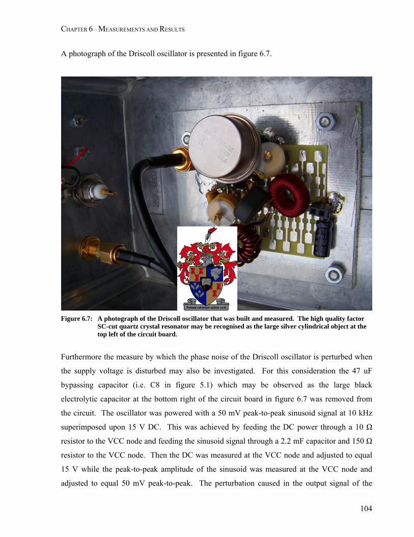
CHAPTER 6 – MEASUREMENTS AND RESULTS
A photograph of the Driscoll oscillator is presented in figure 6.7.
Figure 6.7: A photograph of the Driscoll oscillator that was built and measured. The high quality factor
SC-cut quartz crystal resonator may be recognised as the large silver cylindrical object at the top left of the circuit board.
Furthermore the measure by which the phase noise of the Driscoll oscillator is perturbed when
the supply voltage is disturbed may also be investigated. For this consideration the 47 uF
bypassing capacitor (i.e. C8 in figure 5.1) which may be observed as the large black
electrolytic capacitor at the bottom right of the circuit board in figure 6.7 was removed from
the circuit. The oscillator was powered with a 50 mV peak-to-peak sinusoid signal at 10 kHz
superimposed upon 15 V DC. This was achieved by feeding the DC power through a 10 Ω
resistor to the VCC node and feeding the sinusoid signal through a 2.2 mF capacitor and 150 Ω
resistor to the VCC node. Then the DC was measured at the VCC node and adjusted to equal
15 V while the peak-to-peak amplitude of the sinusoid was measured at the VCC node and
adjusted to equal 50 mV peak-to-peak. The perturbation caused in the output signal of the
104

CHAPTER 6 – MEASUREMENTS AND RESULTS
Driscoll oscillator by the sinusoid was then measured with a spectrum analyser. The result
may be seen in figure 6.8.
9.975 9.98 9.985 9.99 9.995 10 10.005 10.01 10.015 10.02 10.025-90
-80
-70
-60
-50
-40
-30
-20
-10
0
10
20Effect of power supply noise on oscillator output (15 VDC + 50 mVpp (AC))
Frequency [MHz]
Osc
illato
r out
put s
igna
l lev
el [d
Bm]
-54.9923 dBm
11.6128 dBm
-55.334 dBm
Figure 6.8: Output signal of Driscoll oscillator as affected by 50 mV (peak-to-peak) power supply
perturbation at 10 kHz.
Each of the two signals 10 kHz away from the carrier in figure 6.8 consists of half phase noise
and half amplitude noise. How the single sideband phase noise is affected may be quantified
by considering half of the average of the two signals 10 kHz away from the carrier. This was
done for small applied disturbances of 30 mV, 40 mV, 50 mV, 60 mV, 70 mV and 80 mV at 10
kHz and the result is displayed in figure 6.9. In this figure the linear relationship between the
amplitude of an applied disturbance to the phase noise at the corresponding offset frequency
may be seen with comparison to a least squares linear fit to the data. From the least squares
linear fit to the data an approximate equation may be written to quantify this relationship:
( ) ( ) ( ) [ ]dBc/Hzofunitsin)20.79(42.1 )( −⋅≈ fPf dBmedisturbancdisturbedL (6.2)
105

CHAPTER 6 – MEASUREMENTS AND RESULTS
-36 -35 -34 -33 -32 -31 -30 -29 -28 -27 -26-72
-70
-68
-66
-64
-62
-60
-58
Perturbation signal power [dBm]
Phas
e no
ise
dist
urba
nce-
to-c
arrie
r rat
io [d
Bc]
Relationship between the perturbation signal power and the phase noise distrubance at 10 kHz
Measured dataLeast squares fit
Figure 6.9: The affect of perturbation power (at 10 kHz superimposed on DC power supply) on the phase
noise sidebands.
6.3. Conclusion
Figure 6.6 shows the central measurement of this thesis. From a comparison of the measured
phase noise for the Driscoll oscillator with the residual system noise it is clear that the residual
phase noise of the measurement system limits the sensitivity by which the phase noise of the
oscillator can be determined for all offset frequencies greater than 20 Hz. Consequently it is
likely that the phase noise of the oscillator is lower than that of the residual phase noise of the
system – the exact difference can only be determined with phase noise measurement equipment
superior to that available to the author. Nevertheless, the ultimate phase noise may be read
from the graph at offset frequencies between 500 kHz and 600 kHz and agrees well with the
ultimate phase noise calculation according to Leeson’s equation (which is plotted on the same
graph as the dashed line).
106

CHAPTER 6 – MEASUREMENTS AND RESULTS
Determining the resonator bandwidth to confirm the loaded quality factor of the resonator from
the measurement cannot be done because the residual system noise is above that of the
oscillator in this region.
For offset frequencies less than 20 Hz the measured phase noise of the Driscoll oscillator is
more than that of the residual system noise. In this region the measurement reflects the phase
noise of the Driscoll oscillator rather than that of the measurement system. It is noted that the
decreasing slope of the phase noise in this region is -50 dB/decade. As Leeson’s phase noise
model only predicts phase noise with a steepest slope of -30 dB/decade the deviation of the
measured phase noise from the predicted phase noise in this region the predicted phase noise in
this region is deemed no longer valid. That is, Leeson’s phase noise model does not claim to
predict such close in phase noise.
It was shown how the residual system noise can be measured by using a quadrature hybrid.
From this measurement regions over which the phase noise measurement is on or below the
residual system noise may be identified. In these regions measured phase noise is likely lower
than the measurement shows but no further conclusions may be reached.
The effect that noise perturbations on the DC power supply to the Driscoll oscillator has on the
phase noise was quantified. This allows for further design iterations to be pursued in order to
reduce the sensitivity of the oscillator to noise on the power supply.
Finally a comparison of the measured phase noise of the Driscoll oscillator with a commercial
ultra-low phase noise oscillator by Wenzel Associates, Inc. which also operates at 10 MHz is
shown in figure 6.10. Both oscillators yield an output of 13 dBm into a 50 Ω load and makes
use of SC-cut quartz crystal resonators. Notice that for offset frequencies less than 100 Hz the
measurement shows that the Driscoll oscillator that was designed for this oscillator is superior
to that of Wenzel’s oscillator. Over the remainder of the Wenzel oscillator’s given phase noise
specification* (offset frequencies of 100 Hz to 10 kHz) the phase noise of the Wenzel oscillator
* This phase noise specification was published by Wenzel Associates, Inc on their website at www.wenzel.com (10 Feb. 2007).
107
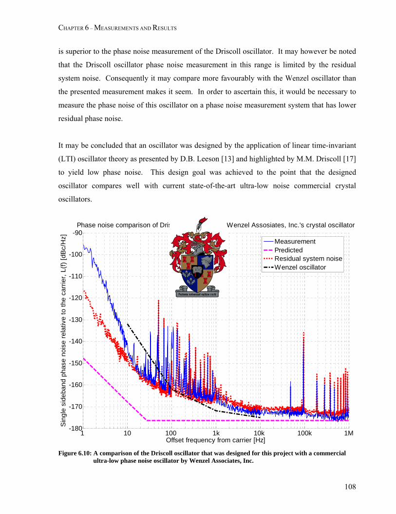
CHAPTER 6 – MEASUREMENTS AND RESULTS
is superior to the phase noise measurement of the Driscoll oscillator. It may however be noted
that the Driscoll oscillator phase noise measurement in this range is limited by the residual
system noise. Consequently it may compare more favourably with the Wenzel oscillator than
the presented measurement makes it seem. In order to ascertain this, it would be necessary to
measure the phase noise of this oscillator on a phase noise measurement system that has lower
residual phase noise.
It may be concluded that an oscillator was designed by the application of linear time-invariant
(LTI) oscillator theory as presented by D.B. Leeson [13] and highlighted by M.M. Driscoll [17]
to yield low phase noise. This design goal was achieved to the point that the designed
oscillator compares well with current state-of-the-art ultra-low noise commercial crystal
oscillators.
1 10 100 1k 10k 100k 1M -180
-170
-160
-150
-140
-130
-120
-110
-100
-90
Offset frequency from carrier [Hz]
Sin
gle
side
band
pha
se n
oise
rela
tive
to th
e ca
rrie
r, L(
f) [d
Bc/
Hz]
Phase noise comparison of Driscoll oscillator with Wenzel Assosiates, Inc.'s crystal oscillator
MeasurementPredictedResidual system noiseWenzel oscillator
Figure 6.10: A comparison of the Driscoll oscillator that was designed for this project with a commercial
ultra-low phase noise oscillator by Wenzel Associates, Inc.
108
Chapter 7
General conclusion
7.1. Conclusion
In the first part of this thesis an introduction to phase noise theory and measurement was
presented for the engineer unfamiliar with this specialised field. This presentation was directed
at meeting the need of engineers who feel excluded from the field of crystal oscillator design
for low phase noise due to a lack of knowledge.
The simplest of the phase noise theories that was presented in the first part of this thesis was
the linear time-invariant (LTI) theory of D.B. Leeson [13]. This theory, together with design
guidelines outlined by M.M. Driscoll [17], was applied to the design of a low-phase noise
quartz crystal oscillator at 10 MHz.
The designed oscillator yielded satisfactorily low phase noise that compares favourably with
commercial ultra-low phase noise crystal oscillators. The measured phase noise of the
oscillator that was designed was limited by the residual phase noise of the measurement
system. Consequently, if a phase noise measurement system with improved residual system
noise was available, the phase noise of the designed oscillator could have been shown to be
even lower.
An important part of low-phase noise measurements is to determine the residual phase noise of
the phase noise measurement system as to ascertain the reliable range of measurement data.
This was achieved by the use of a quadrature hybrid of which the design and construction was
presented. The measurement setup to find the residual system noise through the use of a
quadrature hybrid was also outlined in this thesis.
109

CHAPTER 7 – GENERAL CONCLUSION
Finally it was shown how noise on the power supply causes phase noise around the carrier and
how this process may be quantified.
In conclusion it may be noted that if extremely low phase noise is required it is best to design
an oscillator to conform closely to linear operational requirements by restricting all non-linear
behaviour to occur within a sub-circuit designed specifically for this behaviour (to contribute
minimally to 1/f flicker of phase noise). By meeting this requirement application of low-phase
noise oscillator design by Leeson’s phase noise theory follows.
7.2. Recommendations
Although phase noise measurement equipment is known to be exceedingly expensive it is
highlighted that further investigations into ultra-low phase noise crystal oscillators demands
phase noise measurement equipment with associated residual phase noise superior to that
available to the author. Perhaps a simple, inexpensive system can be designed by which the
phase noise can be measured accurately at a single operating frequency.
For commercial oscillators it may be important to load the oscillator with a buffer amplifier
instead of assuming a 50 Ω load as was the case for the oscillator that was designed for this
project as the output load may not guaranteed. By following through on repeated design
iterations the effect that noise on the power supply has on the phase noise may be reduced for
commercial oscillators where a low noise DC supply is not guaranteed. This may be done
according to the quantification of this process which was outlined in chapter 6.
An ultra-low phase noise crystal oscillator was designed by application of linear time-invariant
phase noise theory that compares favourably to commercial products. It is hoped that the
design concepts together with the presented phase noise theory and measurement techniques
would draw more engineers to this challenging field of study.
110

Appendix A
A Detailed discussion of the phase demodulation method of measuring
phase noise
Figure A.1: Block diagram of the phase demodulation method of measuring phase noise
Figure A.1, above, shows a block diagram of the phase demodulation method and is simply a
copy of figure 4.4 which is duplicated here for easy reference. To understand how this method
of phase noise measurement works and why its various constraints apply, an understanding of
how a mixer can be employed as a phase detector is essential.
A.1 Characteristic of a double balanced mixer which is used as a phase detector
When a double balanced mixer is used as a phase detector a characteristic relation between the
output voltage to the phase difference of the two input sources may be plotted. Such a relation
may be seen in figure A.2 below. Notice that the gradient of this phase voltage characteristic is
a maximum when the phase difference is 2π radians (that is phase quadrature). Stated
111

APPENDIX A – DETAILED DISCUSSION OF THE PHASE DEMODULATION METHOD OF MEASURING PHASE NOISE
differently, the sensitivity of a double balanced mixer to phase fluctuations of its input sources
is a maximum when the input sources are in phase quadrature with respect to each other.
Also note that at this quadrature point, the gradient of the phase voltage characteristic is fairly
constant. Such a property allows for a locally linearized approximation to be a good
approximation to a non-linear relationship (over a limited range of course). A simple
derivation of exactly how the output voltage of such a mixer can be related to the phase
difference of the input sources together with the calibration constant and calibration procedure
follows in equations A.2 – A.6. First let us consider the importance of the phase quadrature
condition.
Figure A.2: The characteristic curve of a double balanced mixer which is used as a phase detector
As the phase deviation from quadrature, φΔ , at the two input sources to the mixer increases so
also the measurement error of the SSB phase noise relative to the carrier, ( )φΔerrorL , increases
in magnitude [12]:
( ) ( ) ( ) ( ) [ ]dBffmeasurederror φφφ Δ⋅=−Δ=Δ coslog20, LLL (A.1)
where ( )φΔ,fmeasuredL – determined from linearization of the mixer output voltage ( )fL ( )fL – the actual SSB phase noise relative to the carrier
112
APPENDIX A – DETAILED DISCUSSION OF THE PHASE DEMODULATION METHOD OF MEASURING PHASE NOISE
The observation from figure A.2 that the measured phase deviation from quadrature, measuredφΔ ,
is always less than the actual phase deviation from quadrature, φΔ , is the physical cause
dictating the negative sign of the measurement error, ( )φΔerrorL , in equation A.1. For small
phase deviations from quadrature the measurement error is quite small as may be seen in table
A.1 below.
Table A.1: Error function for the phase demodulation measurement method
φΔ [rad] φΔ [˚] ( )φΔerrorL [dB] 0.017 1 -0.001 0.087 5 -0.033 0.175 10 -0.133 0.262 15 -0.301 0.349 20 -0.540
To ensure that measurements are reliable, it is important that the phase quadrature condition be
monitored. Such monitoring is done automatically with the Aeroflex PN9000B Phase Noise
Measurement System that was used for phase noise measurements in this project. This
measurement system would monitor the phase quadrature condition and alert the user when the
quadrature condition is no longer sufficient so that the measurement setup may be modified
and new measurements taken.
A final conclusion to be drawn from the importance of maintenance of the phase quadrature
conditions is that the two input sources to the mixer must be at the same frequency. If this is
not met, the phase difference will increase linearly leading to a periodically [at the beat (or
difference) frequency of the two sources] increasing and decreasing error function that would
yield invalid phase measurement over the largest part of the (beat frequency) cycle. Of course,
both this condition that the two sources must be at the same frequency and the quadrature
phase difference condition is maintained by the phase locked loop (PLL) which can be seen in
figure A.1
113

APPENDIX A – DETAILED DISCUSSION OF THE PHASE DEMODULATION METHOD OF MEASURING PHASE NOISE
A.2 Measurement and calibration of the phase fluctuation, φΔ
When the return path of the PLL (which starts after the low pass filter, proceeds through the
PLL amplifier and ends at the actuator of the RO) together with the low noise amplifier and the
PC is ignored in figure A.1, a derivation of the output voltage (after the low pass filter) – phase
deviation relationship may be obtained.
Furthermore, when only the mixer with the two input sources are considered, the output signal
of the mixer (at the intermediate frequency (IF) – port) is described by [12]:
( ) ( ) ( ) ( ) ( ) HOMPttVKttVKtV ROSUTSUTLROSUTSUTLIF +++++−= φωωφωω coscos (A.2)
where – mixer efficiency LK ( )tV SUTSUT ωcos – source under test (SUT) signal ( )[ ttV RORO ]φω +cos – reference oscillator (RO) signal – higher order mixer products HOMP The low pass filter immediately following the mixer strips the signal from higher frequency
components yielding an output signal [12]:
( ) ( ) ( )
( )[ ]( )ttV
ttVKtV
ROSUTpeakb
ROSUT
V
SUTLLPF
peakb
φωω
φωω
+−±=
+−=
cos
cos321
(A.3)
where – peak of the beat frequency (between the SUT and RO) signal SUTLpeakb VKV =
The two conditions governing the implementation of a mixer as a phase detector, as has been
discussed earlier, may be expressed as [12]:
( ) ( ) ( ) ZktktandROSUT ∈Δ+⎟⎠⎞
⎜⎝⎛+== ,
212 φπφωω (A.4)
114
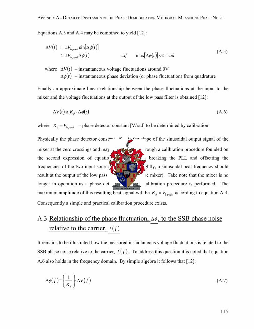
APPENDIX A – DETAILED DISCUSSION OF THE PHASE DEMODULATION METHOD OF MEASURING PHASE NOISE
Equations A.3 and A.4 may be combined to yield [12]:
( ) ( )[ ]
( ) ( )[ ] radtiftV
tVtV
peakb
peakb
1max...
sin
<<ΔΔ±≅
Δ±=Δ
φφ
φ (A.5)
where – instantaneous voltage fluctuations around 0V ( )tVΔ ( )tφΔ – instantaneous phase deviation (or phase fluctuation) from quadrature
Finally an approximate linear relationship between the phase fluctuations at the input to the
mixer and the voltage fluctuations at the output of the low pass filter is obtained [12]:
( ) ( )tKtV φφ Δ⋅≅Δ (A.6)
where – phase detector constant [V/rad] to be determined by calibration peakbVK =φ
Physically the phase detector constant, , is the slope of the sinusoidal output signal of the
mixer at the zero crossings and may be determined through a calibration procedure founded on
the second expression of equation A.3. Through breaking the PLL and offsetting the
frequencies of the two input sources to the mixer slightly, a sinusoidal beat frequency should
result at the output of the low pass filter (following the mixer). Take note that the mixer is no
longer in operation as a phase detector when this calibration procedure is performed. The
maximum amplitude of this resulting beat signal will be
φK
peakbVK =φ according to equation A.3.
Consequently a simple and practical calibration procedure exists.
A.3 Relationship of the phase fluctuation, φΔ , to the SSB phase noise
relative to the carrier, ( )fL
It remains to be illustrated how the measured instantaneous voltage fluctuations is related to the
SSB phase noise relative to the carrier, ( )fL . To address this question it is noted that equation
A.6 also holds in the frequency domain. By simple algebra it follows that [12]:
( ) ( )fVK
f Δ⋅⎟⎟⎠
⎞⎜⎜⎝
⎛≅Δ
φ
φ 1 (A.7)
115
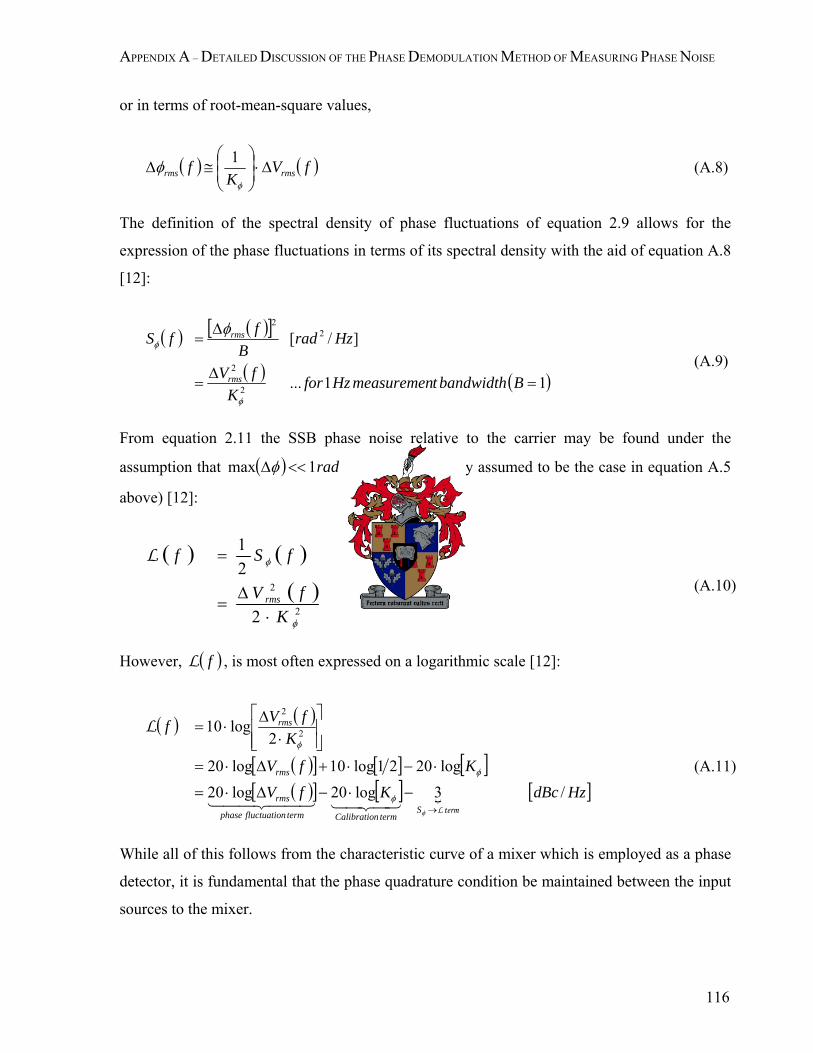
APPENDIX A – DETAILED DISCUSSION OF THE PHASE DEMODULATION METHOD OF MEASURING PHASE NOISE
or in terms of root-mean-square values,
( ) ( )fVK
f rmsrms Δ⋅⎟⎟⎠
⎞⎜⎜⎝
⎛≅Δ
φ
φ 1 (A.8)
The definition of the spectral density of phase fluctuations of equation 2.9 allows for the
expression of the phase fluctuations in terms of its spectral density with the aid of equation A.8
[12]:
( ) ( )[ ]
( ) ( )11...
]/[
2
2
22
=Δ
=
Δ=
BbandwidthtmeasuremenHzforK
fV
HzradB
ffS
rms
rms
φ
φφ
(A.9)
From equation 2.11 the SSB phase noise relative to the carrier may be found under the
assumption that ( ) rad1max <<Δφ (which was already assumed to be the case in equation A.5
above) [12]:
( ) ( )
( )2
2
2
21
φ
φ
KfV
fSf
rms
⋅Δ
=
=L (A.10)
However, , is most often expressed on a logarithmic scale [12]: ( )fL
( ) ( )
( )[ ] [ ] [ ]( )[ ] [ ] [ ]HzdBcKfV
KfV
KfVf
StermnCalibratiotermnfluctuatiophase
rms
rms
rms
/3log20log20log2021log10log20
2log10 2
2
termL
L
→
−⋅−Δ⋅=
⋅−⋅+Δ⋅=⎥⎥⎦
⎤
⎢⎢⎣
⎡
⋅Δ
⋅=
φ
φ
φ
φ
4342144 344 21
(A.11)
While all of this follows from the characteristic curve of a mixer which is employed as a phase
detector, it is fundamental that the phase quadrature condition be maintained between the input
sources to the mixer.
116

APPENDIX B – A TEMPERATURE CONTROLLER FOR QUARTZ CRYSTAL RESONATORS
Appendix B B A temperature controller for quartz crystal resonators A temperature controller was designed in order to establish a phase lock between two crystal
oscillators using high quality factor SC-cut quartz crystal resonators. This was essential to
maintain phase lock over a long period of time which made it possible for phase noise
measurements to be performed on such oscillators at improved resolution. The design of the
temperature controller centred on a precision voltage reference (LM399 at 7 V), a temperature
sensor (LM335) and the power dissipation of a power transistor (TIP41) in the form of heat.
The crystal resonator that was to be heated was fitted to an aluminium block that acted as a
heat tank. Attached to the aluminium block were also the temperature sensor and the power
transistor. A negative feedback controller was designed by controlling the emitter current of
the power transistor with an amplified difference signal between a reference voltage signal and
the temperature sensor signal. The reference voltage was established by voltage division from
the temperature controlled precision voltage reference (LM335). The system had a response
time of approximately 10 seconds. This response time was limited by the rate of heat transfer
from the power transistor, through the aluminium block, to the temperature sensor.
A circuit diagram of the temperature controller (with component values) is presented in figure
B.1 while a photograph of it may be seen in figure B.2. The photograph which is presented in
figure B.2 also shows the crystal resonator (with pins pointing upward) set in the aluminium
block. The hole in the top-middle of the block is where the temperature sensor was fit (which
cannot be seen as it is at the bottom of the block) while the small hole on the right-hand side of
the block is what the power transistor is fitted to with a screw.
117
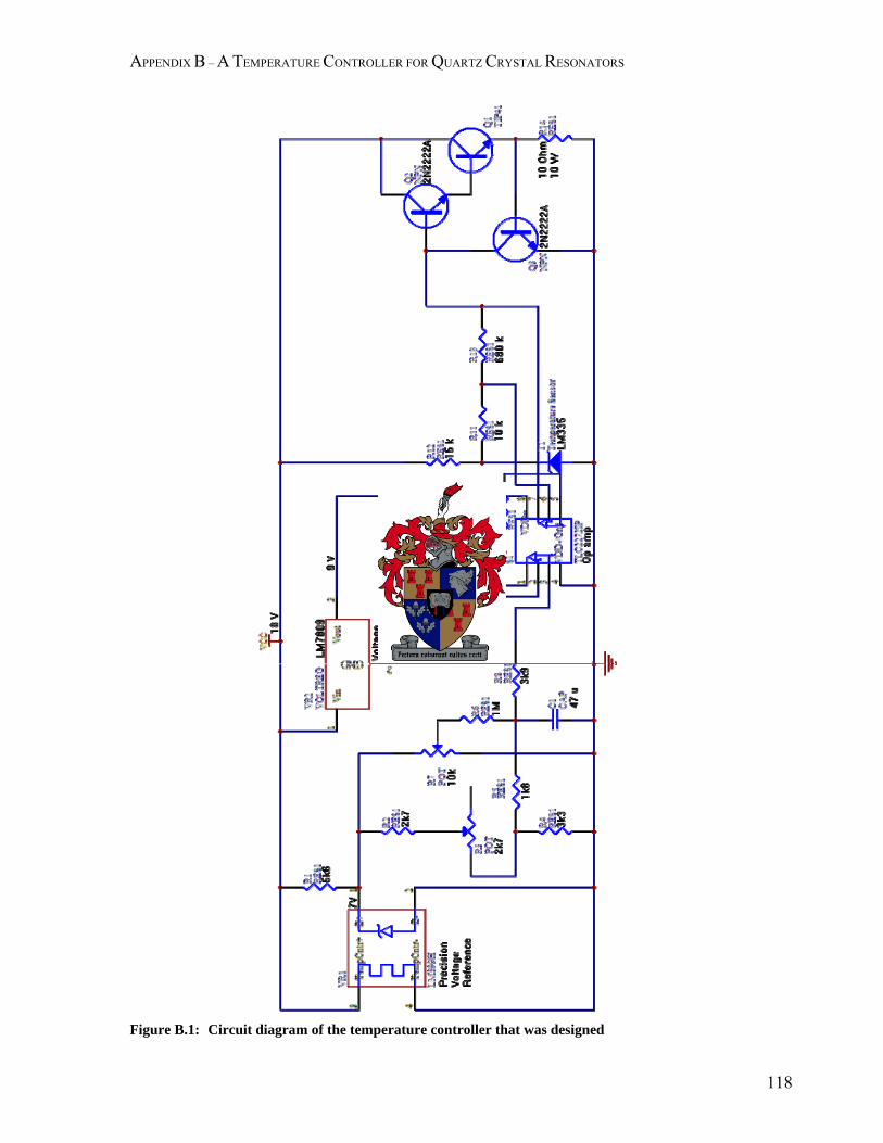
APPENDIX B – A TEMPERATURE CONTROLLER FOR QUARTZ CRYSTAL RESONATORS
Figure B.1: Circuit diagram of the temperature controller that was designed
118

APPENDIX B – A TEMPERATURE CONTROLLER FOR QUARTZ CRYSTAL RESONATORS
Figure B.2: Photograph of temperature controller that was designed to establish long term frequency
stabilisation of the quartz crystal resonators
119

APPENDIX C – DESIGN & IMPLEMENTATION OF A HIGH Q FREQUENCY SELECTABLE QUARTZ RESONATOR
Appendix C C Design and implementation of a strategy to make the high quality
factor quartz crystal resonators frequency selectable
In order for phase noise measurements to be performed with better resolution it was necessary
that the crystal oscillators be built in duplicate and that one of the two oscillators be frequency
adjustable over a small range (such a range of 2.8 Hz around 10 MHz was achieved for high
quality SC-cut quartz resonators). A helpful suggestion by Prof. P.W. van der Walt to create
an equivalent frequency selectable resonator by adding a series inductor-capacitor combination
(of which the capacitance is voltage selectable) in series with one of the SC-cut quartz
resonators was realised and is described here. A circuit diagram of this is presented in figure
C.1.
(b)(a) Figure C.1: Circuit diagram of how the crystal resonator was made frequency selectable
(a) Crystal resonator (b) Equivalent frequency selectable resonator sub-circuit
To control the frequency of this equivalent frequency selectable resonator by applying a
voltage, the BB204G varactor diode from Phillips Semiconductor was used. The capacitance
of this diode may changed over the range 55 pF (when a voltage of 0.8 V is applied) to 23 pF
(when a voltage of 10 V) is applied. Two factors have to be taken into account before this sub-
circuit can be implemented:
• The varactor diode must be completely DC decoupled from the sub-circuit to prevent interference with the biasing of the active element in the oscillator circuit.
• If the varactor diode is the only capacitance used then the circuit would tune over too wide a range of frequencies so that the series resonant point of the crystal would be excluded by that of the series LC-combination. The cessation of oscillatory behaviour follows as the feedback signal path in the oscillator circuit attenuates excessively over all frequencies. This result followed experimentally.
120

APPENDIX C – DESIGN & IMPLEMENTATION OF A HIGH Q FREQUENCY SELECTABLE QUARTZ RESONATOR
A solution that would overcome both of the above difficulties is presented in the circuit
diagram of figure C.2 (b). The fixed frequency crystal resonator of figure C.2 (a) is to be
replaced by the frequency selectable sub-circuit of C.2. (b).
(b)(a)
R2Cv100 kΩ100 kΩ
1 nFC2
1 nFC3
C182 pF
2.14 µH
L1
Vcontrol R1
i1
i2
Figure C.2: Frequency selectable circuit to overcome the problems that were highlighted previously
(a) Crystal resonator (b) Equivalent frequency selectable with varactor diode sub-circuit
This discussion may be followed at the hand of figure C.2 (b). To ensure that most of the small
signal current i2 would pass through the varactor diode the following must hold:
∞→∞→∞→∞→
32
21
,,
CCRR
(C.1)
and
01
11
→=R
CjR
XvCv ω (C.2)
Because of the extremely small leakage current through the varactor diode (50 nA at a
maximum reverse diode voltage of 30 V) the resistors R1 and R2 can indeed be chosen very
large without causing a significant voltage drop. R1 and R2 are chosen: Ω== kRR 10021 .
Then the voltage drop over one of the resistors is: ( ) ( ) mVknARIV leakage 510050 =Ω⋅=⋅= .
This is sufficient for a varactor diode tuning voltage range of 0.8-10 V.
121

APPENDIX C – DESIGN & IMPLEMENTATION OF A HIGH Q FREQUENCY SELECTABLE QUARTZ RESONATOR
Capacitors C2 and C3 are chosen: nFCC 132 == . This choice ensures reliable capacitor
operation with available ceramic capacitors at 10 MHz. This choice of capacitors could have
been extended to 33 nF, but improvement in the ratio 1R
X C is minimal. With the chosen values
for capacitances C2 and C3 the ratio of equation C.2 at 10 MHz amounts to 159000.01
≈RX C .
This ratio is sufficiently small to ensure that the capacitance would provide the path of least
impedance for the small signal current i2.
Furthermore consider the ratio of equation C.2 (for the least value of varactor capacitance at 10
MHz): 92006.01
≈R
X vC . This is also sufficiently small to ensure that the varactor capacitance
would provide the path of least impedance for the small signal current i2 instead of through the
resistors R1 and R2.
C1 can be chosen to determine how by how much the capacitance of the varactor diode would
affect the equivalent capacitance in series with the inductor, L1. Experimentally it was found
that a value of allows for a 2.8 Hz adjustment in the frequency of the high quality
factor SC-cut quartz crystal resonators.
pFC 821 =
With a value for C1 established, L1, is calculated by application of the series resonant LC-
equation:
equivalentCL 211ω= (C.3)
Working with the middle value for the varactor capacitance of 39 pF the equivalent
capacitance, Cequivalent, may be found: pF
CCC
CC
v
equivalent 18.1181111
32
1 ≈++
+= . It follows
that L1=2.143 μH.
122

References [1] A. Hajimiri and T.H. Lee, “A General Theory of Phase Noise in Electrical
Oscillators”, IEEE Journal of Solid-State Circuits, vol. 33, no. 2, pp. 179-194, Feb 1998
[2] J. Everard, Fundamentals of RF Circuit Design (with Low Noise Oscillators),
Chapter 4, John Wiley & Sons [3] T. Hajder, “Higher Order Loops Improve Phase Noise of Feedback Oscillators”,
Applied Microwave & Wireless, pp. 24-31, Oct 2002 [4] H. McPherson, “An X-band Frequency Agile Source with Extremely Low
Phase Noise for Doppler Radar”, [5] A.A. Abidi, Analog Circuit Design – RF Analog-to-Digital Converters; Sensor
and Actuator Interfaces; Low-Noise Oscillators, PLLs and Synthesizers, Kluwer Academic Publishers, 1997
[6] A. Demir, A. Mehrotra & J. Roychowdhury, “Phase Noise in Oscillators: A
Unifying Theory and Numerical Methods for Characterization”, IEEE Transactions on Circuits and Systems – I: Fundamental Theory and Applications, vol. 47, no. 5, pp. 655-674, May 2000
[7] E. Hafner, “The Effects of Noise in Oscillators”, Proceedings of the IEEE, vol.
54, no. 2, pp. 179-198, Feb 1966 [8] C.D. Motchenbacher & F.C. Fitchen, Low-Noise Electronic Design, John Wiley
& Sons, Inc, 1973 [9] Comstron International/EuropTest, Application Note 93-0001 – Phase Noise
Theory and Measurement, 23 July 1993 [10] Hewlett Packard, Application Note 57-1: Fundamentals of RF and Microwave
Noise Figure Measurements, date unavailable [11] T.H. Lee & A. Hajimiri, “Oscillator Phase Noise: A Tutorial”, IEEE Journal of
Solid-State Circuits, Vol. 35, No. 3, pp. 326-336, Mar 2000 [12] Hewlett Packard, Product Note 11729B-1: Phase Noise Characterization of
Microwave Oscillators – Phase Detector Method, publication date unavailable
123

[13] D.B. Leeson, “A Simple Model of Feedback Oscillator Noise Spectrum”, Proceedings of the IEEE, vol. 54, pp. 329-330, Feb 1966
[14] E. Hegazi, J. Rael & A. Abidi, The Designer’s Guide to High-Purity
Oscillators, Kluwer Academic Publishers, 2005. ISBN 1-4020-7666-5 [15] TH Lee & A Hajimiri, “Corrections to ‘A General Theory of Phase Noise in
Oscillators’”, IEEE Journal of Solid-State Circuits, Vol. 33, No. 6, pp. 928, Jun 1998
[16] D.M. Pozar, Microwave Engineering (Second Edition), John Wiley & Sons,
Inc., 1998 [17] M.M. Driscoll, “Two-Stage Self-Limiting Series Mode Type Quartz-Crystal
Oscillator Exhibiting Improved Short-Term Frequency Stability”, IEEE Transactions on Instrumentation & Measurement, vol. 22, No. 2, pp. 130-138, June 1973
[18] STC Frequency Technology, Frequency Control Products, Quartz Crystals –
product information, date unavailable [19] Hewlett Packard, “Fundamentals of Quartz Oscillators”, Application note 200-2,
1997 [20] J.R. Vig, A Tutorial for Frequency Control and Timing Applications, IEEE
website, http://www.ieee-uffc.org/freqcontrol, June 2003, document reference number: SLCET-TR-88-1 (Rev. 8.5.1.7)
[21] J.R. Vig, Introduction to Quartz Frequency Standards, IEEE website,
http://www.ieee-uffc.org/freqcontrol/quartz/vig/vigtoc.htm, Oct 1992, document reference number: SLCET-TR-92-1 (Rev. 1)
[22] E.A. Gerber, “State of the Art – Quartz Crystal Units and Oscillators”,
Proceedings of the IEEE, vol. 54, no. 2, pp. 103-116, Feb 1966 [23] D.A. Neamen, Electronic Circuit Analysis and Design – 2nd Edition, McGraw-
Hill, 2001 [24] R.W. Rhea, Oscillator Design and Computer Simulation, Noble Publishing
Corporation, 2000 [25] H.A. Haus & J.R. Melcher, Electromagnetic Fields and Energy, Prentice-Hall
Inc., 1989
124

[26] D.A. Howe, Frequency Domain Stability Measurements: A Tutorial
Introduction, Time and Frequency Division, Institute for Basic Standards,
National Bureau of Standards, U. S. Department of Commerce, March 1976
[27] D.A. Howe, D.W. Allan, & J.A. Barnes, “Properties of Oscillator Signals and
Measurement Methods”, from the website of NIST as was found on 10 March
2005 at www.boulder.nist.gov/timefreq/phase/Properties/main
[28] D.A. Howe, D.W. Allan, & J.A. Barnes, “Properties of Signal Sources and
Measurement Methods”, Time and Frequency Division, U. S. National Bureau
of Standards, Proceedings of the 35th Annual Symposium on Frequency Control,
1981
[29] The IEEE Standard Dictionary of Electrical and Electronics Terms, 6th Edition
(IEEE Standard 100-1996), Authored by the 10th Standards Coordinating
Committee for Terms and Definitions, 8 April 1997.
[30] E.S. Ferre-Pikal, J.R. Vig, J.C. Camparo et al, “Draft Revision of IEEE Std
1139-1988 Standard Definitions of Physical Quantities for Fundamental
Frequency and Time Metrology – Random Instabilities”, IEEE International
Frequency Control Symposium, pp. 338-357, 1997
125
Copyright © 2022 FDOKUMEN