Lesson 1. Surveying – Introduction Introduction to Surveying ...
Upload
khangminh22Category
view
1download
0
3
INTRODUCTION
FEATURES
1. General1) Enhanced IDE interface.2) Internal 5.25 inch, halfheight CD-R/RW Drive.3) 8 Mbytes (or 2Mbytes) buffer memory.4) Audio CD like tray loading of a disc without using a caddy.5) Power loading and power ejecting of a disc. The disc can also be ejected manually.6) Supports Power saving mode and Sleep mode.7) Vertical and Horizontal operation.8) SuperLink Function.
2. Supported disc formats1) Reads and writes data in each CD-ROM, CD-ROMXA, CD-I FMV, Video CD, and CD-EXTRA2) Reads data in Photo CD (Single and Multi session).3) Reads and writes standard CD-DA.4) Reads and writes CD-R discs conforming to “Orange Book Part 2”.5) Reads and writes CD-RW discs conforming to “Orange Book Parts 3”.
3. Supported write method1) Disc at once (DAO), Session at once (SAO), Track at once (TAO), Variable packet, Fixed packet, and
Multi-session.
4. Performance1) Random 100 ms average access time.2) CD-R Record speed : 8X, 12X, 16X, 20X~40X (PCAV).3) CD-RW Record speed : 4X, 10X, 12X.4) CD-ROM : Max 6,000 KB/s(Max 40x) Sustained Transfer rate.5) Supports real time error correction and real time layered error correction at each speed.6) PIO Mode 4, Multi DMA Mode 2 .7) Multimedia MPC-3 Spec compliant.8) Support CD-TEXT read/write.
5. Audio1) Output 16 bit digital data over ATA interface.2) 8 Times Digital Filter for CD Audio 3) Software Volume Control4) Equipped with audio line output and headphone jack for audio CD playback.5) Front panel Volume Control for Headphone Output.
This service manual provides a variety of serviceinformation.It contains the mechanical structure of the CD-R/RW Drive and the electronic circuits inschematic form. This CD-R/RW Drive wasmanufactured and assembled under our strictquality control standards and meets or exceedsindustry specifications and standards.This CD-R/RW drive is an internal drive unitdesigned for use with IBM PC, HP Vectra, or
compatible computer. It can write as much as 700Mbytes of digital data into CD-R/RW disc, and canread as much as 650 Mbytes of digital data storedin a CD-ROM, CD-R and CD-RW disc.This CD-R/RW Drive can easily meet theupcoming MPC level 3 specification, and itsEnhanced Intelligent Device Electronics (E-IDE)and ATAPI interface allows Plug and playintegration in the majority of today’s PCs withoutthe need of an additional interface card.

LOCATION OF CUSTOMER CONTROLS
6
1. Disc trayThis is the tray for the disc. Place the disc on theejected disc tray, then lightly push the tray (orpush the eject button) and the CD will be loaded.NOTE: Don’t pull out or push in the disc trayforcibly. This might cause damage to the loadingsection of the drive.
2. Stop/Eject buttonThis button is pressed to open the CD tray.This button works only when power is supplied tothe drive.If an Audio CD is playing, pressing this button willstop it, and pressing it again will open the tray.
3. Emergency Eject HoleInsert a paper clip here to eject the Disc traymanually or when there is no power.
4. Volume controlThis is used to adjust the output volume of theheadphone jack. It can’t be used to adjust theoutput volume for the audio output connectors onthe rear panel.NOTE : Turn the volume down before turning onthe power. Sudden loud noises can damage yourhearing.
5. Headphone jackThis jack is for connecting headphones or mini-speakers.
6. Drive activity indicatorsTwo colored LEDs are used to indicate theoperation of CD-R/RW Drive.(1) ReadThe orange color is displayed when the spindlemotor begins the Spin up operation: accessingdata, reading data, playing Audio, and up loadingtray.(2) WriteThe green color is flashed during disc writingsessions.
READREAD WRITEWRITE
Headphone Jack
VolumeControl Drive Activity Indicators
Stop/Eject Button
Disc Tray
Emergency Eject Hole
Front Panel

7
1. Power ConnectorConnects to the power supply (5-and 12-V DC) ofthe host computer.NOTE : Be careful to connect with the properpolarity. Connecting the wrong way may damagethe system (and is not guaranteed). Usually thisconnector can only be attached one-way.
2. IDE Interface ConnectorConnect to the IDE (Integrated DeviceElectronics) Interface using a 40-pin flat IDEcable.NOTE : Do not connect or disconnect the cablewhen the power is on, as this could cause a shortcircuit and damage the system. Always turn thepower OFF when connecting or disconnecting thecable.
3. Jumper ConnectorThis jumper determines whether the drive isconfigured as a master or slave. Changing themaster-slave configuration takes effect afterpower-on reset.
4. Analog Audio Output ConnectorProvides output to a sound card (analog signal).Generally you need this to play a regular audioCD.
5. Digital Audio Output ConnectorProvides output to a sound card (digital signal).
Digital Audio OutputConnector
Jumper Connector
Analog Audio Output Connector IDE Interface Connector
Power Connector
Rear Panel
1. CABINET and CIRCUIT BOARDDISASSEMBLY
1-1. Bottom ChassisA. Release 4 screws (A) and remove the Bottom Chassis
in the direction of arrow (1). (See Fig.1-1)
1-2. Front Bezel Assy A. Insert and press a rod in the Emergency Eject
Hole and then the CD Tray will open in the directionof arrow (2).
B. Remove the Tray Door in the direction of arrow (3) by pushing the stoppers forward.
C. Release 3 stoppers and remove the Front Bezel Assy.
1-3. Cabinet and Main Circuit BoardA. Remove the Cabinet in the direction of arrow (4).
(See Fig. 1-3)B. Release 2 hooks (a) and remove the CD Tray
drawing forward.C. Remove the Main Circuit Board in the direction of
arrow (5).D. At this time, be careful not to damage the 4
connectors, are positioned at right side, of the MainCircuit Board.
2. MECHANISM ASSY DISASSEMBLY2-1. Pick-up UnitA. Release screws (B).B. Separate the Pick-up Unit in the direction of arrow (6).
(4)
(5)
MainCircuit Board
Cabinet
Hooks (a)
(A)
(A) (A)
(A)
(1)
Bottom Chassis
(2)
(3)
Tray Door
CD Tray
Front Bezel Assy
Emergency Eject Hole
Stoppers
Fig. 1-1
Fig. 1-2
DISASSEMBLY
8
Fig. 1-3
Mechanism Assy
Pick-up Unit(6)
(B)(B)
Fig. 2-1

2-2. Pick-upA. Release 2 screws (C) and remove the Pick-up.
Pick-up Unit
Pick-up
(C)(C)
Fig. 2-2
9

TROUBLESHOOTING GUIDE
Power check (Malfunction of LED and Tray)
55
Check the connection of 5V, 12V.Check the Reset (Pin 170, 122 of
IC101, pin2 of IC401)Check the input of oscillation (pin
109 of IC401)
Check SCLK, SDATA, XLAT (pin 122, 123, 124 of IC401)
1. Connect only the power cable
BD7907FS6Ch Servo DRIVE
MT1516RF AmpWobbleALPC
General port useEEPROM access
MT1508
DSPDecoderEncoder
ATIP DemodulatorWrite Strategy
Write S/H SignalI / F
Micro Processor
33.8688MHz
IC 101
IC 501 IC 103
IC 401
IC 102
3.3 V
Reset
12V 5V
AT49F002N512KB
Flash ROM
IC 50241
109
44
2
54
31
3
32
10 19 20
31
32
30
44 51 IC 202
2 170 PRST‘ L ’
122/ HRST‘ H ’
74 75
MCLK
55‘ H ’
/XRST
SDRAM
123
124
122
63
62
65SCLK
SDATA
XLAT
CN 100

56
Check the Reference voltage(+/- 10%)
Check VC (1.4V) of Drive IC (pin27 of IC501)
Check voltage of VREF(1.4V)(pin 53 of IC101, pin 27 of IC501)
Check voltage of 2VREF(2.8V)(pin 52 of IC101)
Check HAVC/PDVC(2.0V)(pin 34 of IC401, pin 13 of CN201)
Check FVREF/FPDVC (2.8V) (pin 52 of IC401, pin22 of CN201)
Check FPDO(2.8V)(pin 54, 65 of IC401)
BD7907FS6Ch Servo DRIVE
MT1516 RF Amp Wobble ALPC
General port use EEPROM access MT1508
DSPDecoderEncoder
ATIP DemodulatorWrite Strategy
Write S/H SignalI / F
Micro Processor
IC 101
IC 501
CN 201
2.5 V
NJM3414
IC 503
76
75
32
1
IC 506
3
VHAVC
2VREF522.8 V
V28
IC 401
76 VREF531.4 V
V14
27
2
1.4 VVC
OpticalPick-upKRS-330B
LDDrive
17 28 76 134 1803.3 V
34
13
74
52
22
2.0 V
2.8 V
HAVC
VFVREF
FVREF
FPDVC
19FPDO 54
65
FPDO
FPDOLP
PDVC
20
FPDVcc
5 V
2.8V

57
Check the initial operation(Power-on state)
• Check the operating signal of Sled(pin 28, 29 of IC501 : SLIN1, 2)
• Check the output signal of Sled(pin 34, 35, 36, 37 of IC501)
• Check /SLEDIN_SW. (pin 104 of IC401)
• Check the control signal of DriverIC(pin 22, 23 of IC501)
• Check the power of DRIVE ICand VC
Check SCLK, SDATA, XLAT (pin 122, 123, 124 of IC401)
Sled move to inside
Spindle motor rotate
Laser On Check the Laser
• Check the Spindle signal(pin 24 of IC501 : SPIN)
• Check FG input(pin 20 of IC101)
• Check the Hall signal(pin 1, 2, 3, 4, 5, 6 of IC501)
Check the operation of FocusFocus up / Down
Laser Off / Spindle Stop
BD7907FS6Ch Servo
DRIVE
MT1508DSPI / F
Micro Processor
IC 101
IC 501
FMO
271.4 V
VC
2021FG FG
2524SPIN DMO
18
11
9
OpticalPick-upKRS-330B
STEP Motor
SpindleMotor
65
4
23
CTL2
22
CTL1
29SLIN2
28SLIN1
373635
3
21
U
V
W
HU+ , HU-
7HB
B+ A- A+
27
26
FMO2
MT1516ALPC
General port use
IC 401
102101
123
124
122
63
62
65SCLK
SDATA
XLA T
DR
V-M
UT
E2
DR
V-M
UT
E1
HV+ , HV-
HW+ , HW-
,
,
,
34
B-
104
(From pin 1 of CN402)
/SLEDIN_SW
2 times iteration
58
1. Waveform when Sled moves to inside
SLIN1/SLEDINSW
A+
2. Waveform of Spindle rotation
HU+HV+HW+
3. Waveform of Spindle Kick
SPINFGU
Zoom in wave
Zoom in wave
Zoom in wave
Zoom in wave
When the sled moves to the inner position,the sine wave(refer to Fig1) inputs toSLIN1/SLIN2 (the input pins of drive IC).When Pick-Up unit approached to innermostposition, the /SLEDINSW signal(CN402 pin 1)becomes 0 V.The output pins A+ ,A-, B+, B- of the drive IC isPWM waveform and drives the Stepping Motor.
The output signal of Hall(HU+, HU-, HV+, HV,HW+, HW-) comes from a Hall sensor of spindlemotor and they were inputted to pin 1, 2, 3, 4, 5, 6of drive IC(BD7907FS) via CN402. When spindlemotor rotate, HU+, HW+, HV+ signals aregenerated in a regular order with 1200 phase delayeach other.(Refer Fig 2)
If waveforms of HU+, HU-, HV+, HV-, HW+, HW-different from Fig 2, check the pin 7(HB signal) ofdrive IC. The HB signal must be about 5V.
Wave of U,V,W assigned to pin 9,11,18 of DriveIC is a PWM waveform and they drive Spindlemotor.When spindle motor rotate, U/W/V signals aregenerated in a regular order with 1200 phase delayeach other. (Refer Fig 3)
If waveforms different from Fig 3, check pin27(VC), pin 51(VCC), pin22(CTL1), pin23 (CTL2),R514, R512, R510, R511.
When spindle kick, refer to Fig 4.
Fig.1
Fig.2
Fig.3
Fig.4

59
Check Tray operation
Check /EJECT KEY (pin 11 of IC101)
Check the output signal of tray(pin 49, 50 of IC501)
Check the LED
Check operating signal of tray(pin 26 of IC501)
• Check the control singal of Drive IC(pin 22, 23 of IC501)
• Check the power of DRIVE IC andVC
Check operating signal of LED (pin96, 98 of IC401)
Check SCLK, SDATA, XLAT (pin122, 123, 124 of IC401)
Check operation S/W of tray(/OPEN SW:pin 94 of IC401/LOAD SW : pin 95 of IC401)
M
Tray Motor
MT1516 RF Amp
General port use
IC 401
123
124
122SCLK
SDATA
XLA T
MT1508
DSPDecoderEncoder
I / F
Micro Processor
IC 101
SW103
DETECTOR-TRAY
63
62
65
FR
ON
T
BD7907FS6Ch Servo DRIVE
IC 501
22
101
DRV-MUTE2 DRV-MUTE1
CTL2CTL1
271.4 V
VC
2426LDIN
49
50
SW102
EJECT-SW
11
2
1
94
95
/OPEN_SW
/LOAD_SW
TRAY -
TRAY +
PWMOUT
/EJECT_KEY
LED102
LED101
96
98
Q802
Q801
LED1
LED2
23
102
60
Check identification of Drive
Check the connection of ATAPIcable
Check the communication betweenPC and MT1508 (IC101)
Check SDRAM (IC102)
Check Flash ROM (IC103)
2. Connection of Power and ATAPI cable
MT1508
DSPDecoderEncoder
ATIP DemodulatorWrite Strategy
Write S/H SignalI / F
Micro Processor
HOST
8MBSDRAM
I/Fcable
Address
Data
IC 101IC 103
IC 102
AT49F002N512KB
Flash ROM
33.8688MHz
74 75
Address
Data
Pin no. Pin name Pin no. Pin name39 DASP GND 4037 CS1 CS3 3835 DA0 DA2 3633 DA1 PDIAG 3431 INTRQ IO16 3229 DMACK GND 3027 IORDY CSEL 2825 IOR GND 2623 IOW GND 2421 DMARQ GND 2219 GND KEY 2017 HD0 HD15 1815 HD1 HD14 1613 HD2 HD13 1411 HD3 HD12 129 HD4 HD11 107 HD5 HD10 85 HD6 HD9 63 HD7 HD8 41 /HRST GND 2
CN101(ATAPI)
SDRAM

61
Check the identification of CD-ROM Disc (insert Disc)
Check the operation of Focus
Check the operation of Tracking
Check the Jump action
• Check the drive signal of FCS-/+(pin 1, 2 of CN201)
• Check drive input signal of Focus(pin 53 of IC501 : FCIN)
• Check the input signal of FE(pin 42 of IC101 : FEI)
• Check the input signal of SBAD(pin 38 of IC101)
• Check the input signal of CSI (pin41 of IC401)
• Check the input signal of RFZC (pin60 of IC101 : HRFZC)
• Check the drive signal of TRK+/-(pin 3, 4 of CN201)
• Check the signal of Tracking (pin 52 of IC501 : TKIN)
• Check the signal of SLED(pin 28, 29 of IC501 : SLIN1, 2)
• Check control signal of Drive IC(pin 22, 23 of IC501: CTL1,2)
• Check power and VC of DRIVE IC
Check signal of A~H (pin 39, 38, 37,36, 30, 31, 32, 33 of IC401)
Check the input signal of TE(pin 40 of IC101 : TEI)
In case of Focus Up/Down
MT1516 RF Amp
General port use
IC 401
123
124
122SCLK
SDATA
XLA T
MT1508
DSPDecoderEncoder
I / FMicro Processor
IC 101
63
62
65
BD7907FS6Ch Servo
DRIVE
IC 501
DRV-MUTE2
DRV-MUTE1CTL2
CTL1
271.4 V
VC
45TEO
40
43CSI
41
49SBAD
38
NJM3404
7
IC 505
1
52
53
6
2
23
22
OpticalPick-upKRS-330B
45 46
1 2
47 48
3 4
FC
S-
FC
S+
TR
K+
TR
K-
22
23
101
102
FCIN
TKIN
FOO
TRO
FOSO
TRSO
A ~ D
E ~ H
CN 201
TEI
CSI
SBAD
42FEO
42 FEI
FMO
29SLIN2
28SLIN1
27
26
FMO2
126RFZC
60 HRFZC

62
4. Operation of Focus Up/Down
FESBADFCS+
5. Waveform of Track Following
6. Waveform of Track Jump
TE
EQRF
CE
SLIN1
7. Waveform of Spindle Servo On
SPIN
FG
U
Zoom in wave
Focus Search Focus Servo On
Zoom in wave
Zoom in wave
Waveform of Focus Search refer to Fig 5.In Focus Search, FE signal and SBAD signal areused to Focus Servo On.Therefore, in case of Focusing Fail, check the FEsignal and SBAD signal.
Waveform of Track Following(Sequential Read)refer to Fig 6.By Sled Servo, SLIN1, SLIN2 (pin 28, 29 of DriveIC) drive the Sled Motor(Stepping Motor) forlocating the lens on the center axis of Pick-up.
Waveform of Track Jump refer to Fig 7.Center level of TE,CE is 1.4V.SLIN1, SLIN2 signal (pin 28, 29 of Drive IC)assume the form of Pulse. And they drive the SledMotor(Stepping Motor).RFZC(RF Ripple Zero Cross) signal is Pulse formand it lags behind TE signal 900.
To maintain constant rpm(CAV) or l inearvelocity(CLV), the drives control spindle motor.The Fig 8 shows the waveforms when spindleservo is on.
TERFZC
CESLIN1
Fig.5
Fig.6
Fig.7
Fig.8

63
Check RF and Spindle(Insert CD-ROM Disc)
Check the identification of CD-R Disc(Insert Blank CD-R)
Check the identification of CD-RWDisc (Insert Blank CD-R)
Check EQRF input signal(pin 45 of IC101)
Check the signal of A~H (pin 39, 38,37, 36, 30, 31, 32, 33, of IC401)
Check the operation signal of Spindle(pin 24 of IC501)
Check SCLK, SDATA, XLAT (pin 122, 123, 124 of IC401)
Check FG input(pin 20 of IC101)
Check the input signal of ATFG(pin 69 of IC101)
• Check the control signal of Drive IC(pin 22, 23, of IC501)
• Check power/VC of DRIVE IC
BD7907FS6Ch Servo
DRIVE
MT1508
DSPDecoderEncoder
I / F
ATIP Demodulator
Micro Processor
IC 101
IC 501
271.4 V
VC
2021FG FG
2524SPIN DMO18
11
9
OpticalPick-upKRS-330B
STEP Motor
SpindleMotor
65
4
23
CTL2
22
CTL1
3
21
U
V
W
HU+ , HU-
7HB
MT1516RF AmpWobble
General port use
IC 401
102101
123
124
122
63
62
65SCLK
SDATA
XLA T
HV+ , HV-
HW+ , HW-
,
,
,
A ~ D
E ~ H
DRV-MUTE2 DRV-MUTE1
116 69ATFG
21EQRF
45

64
Check point of Writing
Check the compatibility betweenDrive and Tool
Check Disc state (Fingerprint,Scratch, Dust...)
Check whether or not additionalwriting is allowed.
(Given in the Disc Info of writing tool)
Check Laser 1(Check EEPROM)
Activate ‘Addition Func.’ window inTest Tool(GGOOM4)
Execute ‘S/N’ (Identify SerialNumber)
Execute ‘ALPC Parameters’(Identify ALPC Parameters)
Check the communication line ofEEPROM
Execute ‘C. Laser Power setting’ inTest Tool(GGOOM4)
Check whether or not ‘ALPCParameters is initial value
Check whether or not Disc iswriteable (CD-R/CD-RW)
MT1516
ALPC
EEPROM access
MT1508
DecoderEncoder
Micro Processor
IC 101
110 EEP-CS IC 401
107 EEP-SDATA
123
124
122
63
62
65SCLK
SDATA
XLA T
108 EEP-CLK
AT93C862KB
EEPROM
IC 2031
4DO
CS
3DI
2SLK
(ALPC initial value before ‘Laser Power Setting’)

NG
NG
OK
65
Check Laser 2 (No disc)
Execute ‘E.ALPC Test for AS’ inTest Tool (GGOOM4) (select‘VRDC Loop’, and ‘Trigger’)
E
E
Check Read Laser
Initial value of FPDO : 2.8V +/- 10%
OFF LEVEL
VRDC LEVEL FPD
Execute ‘D. Laser Inspection’ inTest Tool (GGOOM4)
Check the input of ENBL(pin 33 of CN201 : ‘H’)
Check the input of VRDC(pin 25 of CN201 : 0.4~0.8V)
Check the input of FPDO (pin 54,65 of IC401 : FPDO~0.1V)
• Check the input of RLDON(pin 128 of IC401 : ‘H’)
• Check SCLK, SDATA, XLAT(pin 122, 123, 124 of IC401)
Check Reference voltage
NG
F
NG
G
VWDC1 LEVEL FPD
VWDC2 FPD
MT1516
ALPC
MT1508
DecoderEncoder
Write StrategyWrite S/H Signal
Micro Processor
IC 101CN 201
5 ENBL
IC 401
OpticalPick-upKRS-330B
LDDrive
33
0.4~0.8V
19FPDO 54
65
FPDO
FPDOLP
ENBL
FPDO-0.1V
123
124
122
63
62
65SCLK
SDATA
XLAT6325 VRDCOVRDC
128 57RLDON
H
H
66
Execute ‘E.ALPC Test for AS’ inTest Tool(GGOOM4) (Select
‘CD-R Rec Mode’, and ‘Trigger’)
FInspection of CD-R Recording Laser
Execute ‘E. ALPC Test for AS’ inTest Tool (GGOOM4) (Select
‘CD-RW Rec Mode’, and‘Trigger’)
GInspection of CD-RW writing Laser
Chect input of ENBL(pin 33 of CN201 : ‘H’)
• Check input of VWDC1(pin 26 of CN201 : 0.4~1.0V)
• Check input of VWDC2 (pin 27 of CN201 : 0.1~0.5V)
• Check input of WLDON(pin 27 of IC401 : ‘H‘)
• Check SCLK, SDATA, XLAT(pin 122, 123, 124 of IC401)
MT1516
ALPC
MT1508
DecoderEncoder
Write Strategy Write S/H Signal
Micro Processor
IC 101
CN 201
5 ENBL IC 401OpticalPick-upKRS-330B
LDDrive
33
1330
0.4~1.0V
WXRWXR
19FPDO 54
65
FPDO
FPDOLP
ENBL
123
124
122
63
62
65SCLK
SDATA
XLAT
6226 VWDC1OVWDC1
6127 VWDC2OVWDC20.1~0.5V
1531 ODONODON
127 58WLDON
WXR
ODON
FPDO
CD-R Recording Pulse
CD-RW Recording PulseWXR
ODON
FPDO
H
H
• Check input of WXR(pin 30 of CN201 : Pulse)
• Check input of ODON(pin 31 of CN201 : Pulse)
Check input of FPDO(pin 54, 65 of IC401 : Pulse)
Initial value of FPDO :2.8V/-10%)

67
Check Audio signal(Insert Audio Disc)
Identify playback of Audio Disc(Play Mode)
Check Output signal of AUIO L/R(pin 51, 54 of CN100)
Check Output signal of AUDIOL/R (pin 165, 167 of IC101)
Check Output signal of /AUD-MUTE (pin 103 of IC401)
Check SCLK, SDATA, XLAT (pin 122, 123, 124 of IC401)
Check Output signal of AUDIOL/R (pin 1, 7 of IC801)
Check Input signal of AUDIO L/R(pin 3, 5 of IC801)
Check Input signal of /AUD-MUTE (pin 3 of IC801)
Output of Headphone
MT1516 RF Amp
General port use
MT1508DSP
DecoderEncoder
I / FMicro Processor
IC 101
BH3544F
AUDIO AMP
IC 801 103
IC 401
LO165
RO167
AUDIO Line Out
51 54
CN 100
JK101
H-JACK
SB
3
5
3
AudioMute
Circuit
1
7
123
124
122
63
62
65SCLK
SDATA
XLAT
L-CH R-CH
ROUT
LOUT
ROUT
LOUT
/AUD-MUTE
ROUT
LOUT
MUTE
FRONT
68
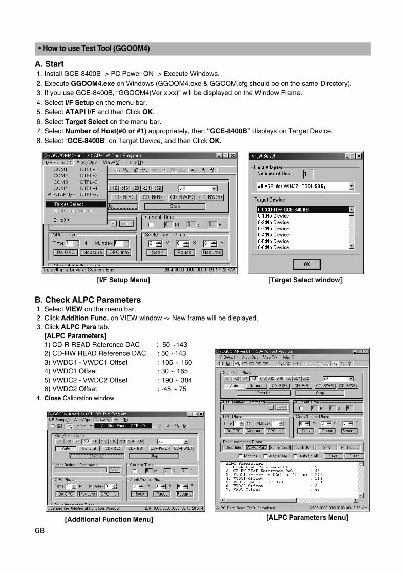
A. Start1. Install GCE-8400B -> PC Power ON -> Execute Windows.2. Execute GGOOM4.exe on Windows (GGOOM4.exe & GGOOM.cfg should be on the same Directory).3. If you use GCE-8400B, “GGOOM4(Ver x.xx)” will be displayed on the Window Frame.4. Select I/F Setup on the menu bar.5. Select ATAPI I/F and then Click OK.6. Select Target Select on the menu bar.7. Select Number of Host(#0 or #1) appropriately, then “GCE-8400B” displays on Target Device. 8. Select “GCE-8400B” on Target Device, and then Click OK.
B. Check ALPC Parameters1. Select VIEW on the menu bar. 2. Click Addition Func. on VIEW window -> New frame will be displayed.3. Click ALPC Para tab.
[ALPC Parameters]1) CD-R READ Reference DAC : 50 ~1432) CD-RW READ Reference DAC : 50 ~1433) VWDC1 - VWDC1 Offset : 105 ~ 1604) VWDC1 Offset : 30 ~ 165 5) VWDC2 - VWDC2 Offset : 190 ~ 3846) VWDC2 Offset : -45 ~ 75
4. Close Calibration window.
• How to use Test Tool (GGOOM4)
[I/F Setup Menu] [Target Select window]
[ALPC Parameters Menu][Additional Function Menu]

C. Laser Power Setup (VWDC1 / VWDC2 re-setup)1. Remove disc on the tray.
2. Select ALPC/OPC on the menu bar, and then select Laser Power Setup menu.
3. Setup LD Power meter (Frequency :780nm, Measure Range : 0.01mW unit).
4. Click VRDC button on the Laser Power Setup window. Laser beam will be emitted from LD.
5. Measure LD Power with LD Power meter. Type the result in the blank(Read Power box).
(If you don’t have LD Power meter, type the written value on pickup without decimal point including two
digits under the decimal point.)
[Ex] 11.34mW ->1134
6. Click VWDC1 button and follow above step 5. But VWDC1 result should be filled in the Write Power box.
7. Click Setup button, and result will be displayed with OK or NG.
8. Close Laser Power Setup window.
69
[Laser Power Setup window]
[Laser Power Setup Frame] [Laser Power Setup Result]

70
[Laser Inspection]
[Laser Power Test Frame] [Laser Power Test Result]
D. Laser Inspection (VRDC/VWDC/FPD Level check)1. Remove disc on the Tray.2. Select ALPC/OPC on the menu bar and select Laser Inspection menu, then Laser Power Test window
will appear.3. Click Trigger button, then the result will be displayed with OK or NG separately.4. Close Laser Power Test window.

72
BD
7907FS
6Ch
Servo
DR
IVE
MT
1516R
F A
mp
Wo
bb
leA
LP
CG
eneral po
rt use
EE
PR
OM
access
MT
1508
DS
PD
ecod
erE
nco
der
AT
IP D
emo
dulato
rW
rite Strateg
yW
rite S/H
Sig
nal
I / F
Micro
Pro
cessor
Au
dio
Mu
teC
ircuit
HOST
33.868MH
zO
pticalP
ick-upK
RS
-330B
SD
RA
M
I/Fcab
le
Data
Address
ST
EP
Motor
FC
ST
RK
Spindle
Motor
Writing
Pulse
Servo S
/H,
Write S
/H S
ignal
Data, C
lock, XLA
TR
eset
Lin
e Ou
t
L,R
AT
93C86
2KB
EE
PR
OM
EQ
RF
,R
RF
,F
EI,T
EI,C
SI
DM
O
FO
OT
RO
SL
O
Address/
Data
PW
M o
ut
F P
DA
BC
DE
FG
HIC
401
IC 101
IC 501
IC 103
IC 102
Au
dio
L,R
3.3 V
Reset
5V
12V
IC 203
AT
49F002N
512KB
Flash
RO
M
LD
Drive
VW
DC
VR
DC
2.5 V
FG
M
Tray M
oto
r
Drive M
ute
LE
D C
on
trol
Mech
anism
S/W
Detect
Functional Block Diagram

MAJOR IC INTERNAL BLOCK DIAGRAM AND PIN DESCRIPTIONIC401 (MT1516) : CD-R/RW Analog Signal Processor
Block Diagram
39
A P C
RFZC1M
CLK
D IG.R E G .
M P X 1
M P X 2
VCON
RR
FX
AD
BC
O
BC
O
AD
O
FPDOX
TELP
MPPO
SPPO
DRCLP
RFRP
MP
X1
TZC
MP
X2
MPX1
ASH
BSH
DSH
ESH
CSH
FSH
GSH
HSH
MP
X2
MP
X2B
VW
DC
2O
VW
DC
1O
VR
DC
O
W R E F 1V W D C 1
V W D C 1 N
F P D O L P
F V R E FF P D O
R R E FV R D C
V R D C N
RF
PD
SH
WF
PD
SH
RLD
ON
WLD
ON
FPDOX
R R F
RR
FX
EQ
RF
GAINUP
SE
RV
SH
WB
LSH
AD
BC
O
AD
OB
CO
FE
O
MP
PO
SB
AD
O
SP
PO
S /H&
M AT R I XR O P C
F ED R C O 2
C ET ES B A DTEIN
R F Z C
S H P CR F Z C 1 V CS H B C
DEFECT
DataSlicer
RE
CD
IN
TEFE
CE
SBADOLP
INA
INB
INC
IND
HAVC
INA
INB
INC
IND
HAVC
INA
INB
INC
IND
HAVC
E Q R F
VC
ON
GAINUP
EQRF
RF
SU
M
MP
XO
UT
1
VR
EF
MP
X
AV D D 1AV S S 1AV D D 2AV S S 2AV D D 3AV S S 3AV D D 4AV S S 4AV D D 5AV S S 5AV D D 6AV S S 6AV D D 7AV S S 7AV D D 8AV S S 8AV D D 9AV S S 9
S DATAX L AT
S C L K DRCSO
DRCMO
SLP
FN
SLP
FP
XD
EF
MD
EF
M
RR
FX
LP
H11
T
I NH
ING
INF
INE
D R C O
INA
HAV
C
IND
INB
INC
T R O P E NT R AYO U T #
TRAYIN#L E D 1L E D 2
LIMIT#F R
E N D MM U T E
S BD E V S E L
E E P _ S DATAE E P _ S C L K
E E P _ C SE N B L
GIO1~GIO7
GeneralI /O
S U B G N D
T R C L O S E
ATIP
10-BitA D C
S E RVO&
Detect ion
SBAD
A S P R E Q
OS
TC
CR
FAG
CC
EQ
BIA
SE
QR
F
RO
PC
CR
OP
CO
AU X 2AU X 3
AU X 1W
RF
SU
M
RR
F
WR
F
RFZC1
TZC
Vol tageRef & DAC
VD
AC
1V
DA
C0
VR
EF
VF
VR
EF
V14
VH
AVC
V28
P /BDetect
x1
MP
XO
UT
2MPX2B
X R S T
DV
SS
2D
VD
D2
DV
SS
1D
VD
D1
S B A D L P
RE
CD
IN/R
RF
SU
M
RR
FX
LPR
RF
/WR
F
ATFMX
FPDO
ROPCO
RFAGCC
FVREF
VRDCB
VWDC1B
WREF1
VRDCO
RREF
WRFSH
AUX1AUX2
AUX3
VWDC1OVWDC2O
VD
AC
0
ATF
G
ATF
M
AG
C3C
AG
C2C
AG
C1C
WB
LCLK

40
• Pin Assignment
Pin Numbers
Symbol Type Description
RF Signals & S/H Control Pulses
36 INA Analog Input Input of Main Beam Signal (A) 37 INB Analog Input Input of Main Beam Signal (B) 38 INC Analog Input Input of Main Beam Signal (C) 39 IND Analog Input Input of Main Beam Signal (D) 30 INE Analog Input Input of Side Beam Signal (E) 31 INF Analog Input Input of Side Beam Signal (F) 32 ING Analog Input Input of Side Beam Signal (G) 33 INH Analog Input Input of Side Beam Signal (H) 34 HAVC Analog Input Reference Voltage Input of Main and Side Beams (2.0V)
120 SERVSH Digital Input (TTL),
SMT S/H Control Pulse of Main and Side Beam Signals
118 WBLSH Digital Input (TTL),
SMT S/H Control Pulse of Wobble Signal
Focus/Tracking Error & Servo Control Signals
40 DRCO Analog Output Output of Differential Radial Contrast (DRC) Signal 41 DRCO2 Analog Input Re-Input of Differential Radial Contrast (DRC) Signal 42 FE Analog Output Output of Focusing Error Signal 45 TE Analog Output Output of Tracking Error Signal 43 CE Analog Output Output of Center Error Signal 49 SBAD Analog Output Output of SBAD Signal 44 TEIN Analog Input Input of Out-of-Track Detection Circuit 50 SBADLP Analog Input Input of SBAD Signal after LPF for DEFECT Detection 46 SHPC Analog Output External Capacitor Connection for Peak Hold of RFRP Signal 47 RFZC1VC Analog Output Reference Voltage for RFRP Peak/Bottom Hold 48 SHBC Analog Output External Capacitor Connection for Bottom Hold of RFRP Signal
126 RFZC Digital Output
(TTL), 4 mA Driving Output of RF Zero Crossing Binary Signal
EQRF (RF Equalizer Filter and Data Slicer) Circuit
19 RFSUM Analog Input Input of RF Summing Signal from PUH to EQRF Block 11 EQBIAS Analog Output External Bias Connection for Circuits in EQRF Block
13 OSTCC Analog Output External Capacitor Connection for Offset Cancellation Circuit of Equalizer Output
16 RFAGCC Analog Output External Capacitor Connection for RF AGC in EQRF Block 21 RFOUT Analog Output Output of RF EFM Signal after Equalizer Filter
4 DEFM Digital Output
(TTL), 6 mA Driving Binary Output of EFM Signal after Slicing (Positive)
3 XDEFM Digital Output
(TTL), 6 mA Driving Binary Output of EFM Signal after Slicing (Negative)
8 SLPFP Analog Input Input ( ) of Auto Slicing Level 9 SLPFN Analog Input Input of Auto Slicing Level
RRF & ROPC (Running OPC) Related Signals
22 RECDIN/ RRFSUM
Analog Input (1). Input of RF Signal for Recorded Area Detection (2). Input of Read RF Summing Signal from PUH to RRF Block
70 RRFXLP Analog Output Low Pass Output of RRF Signal
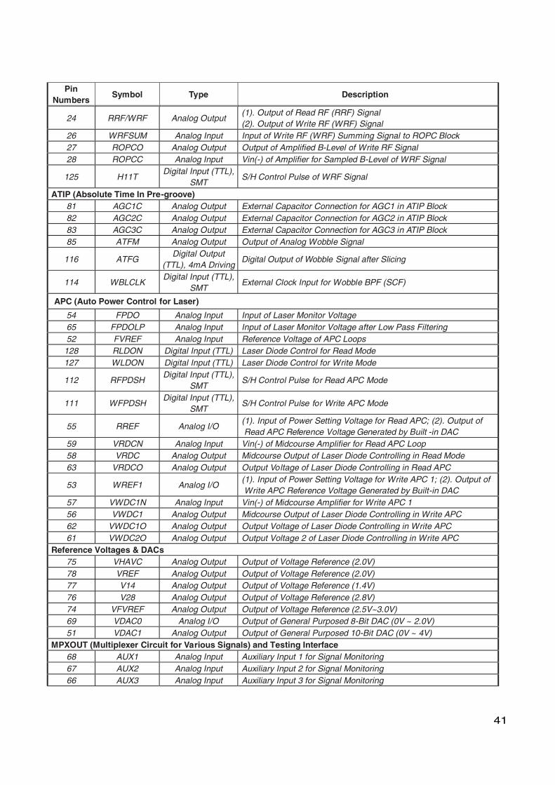
41
Pin Numbers
Symbol Type Description
24 RRF/WRF Analog Output (1). Output of Read RF (RRF) Signal (2). Output of Write RF (WRF) Signal
26 WRFSUM Analog Input Input of Write RF (WRF) Summing Signal to ROPC Block 27 ROPCO Analog Output Output of Amplified B-Level of Write RF Signal 28 ROPCC Analog Input Vin(-) of Amplifier for Sampled B-Level of WRF Signal
125 H11T Digital Input (TTL),
SMT S/H Control Pulse of WRF Signal
ATIP (Absolute Time In Pre-groove) 81 AGC1C Analog Output External Capacitor Connection for AGC1 in ATIP Block 82 AGC2C Analog Output External Capacitor Connection for AGC2 in ATIP Block 83 AGC3C Analog Output External Capacitor Connection for AGC3 in ATIP Block 85 ATFM Analog Output Output of Analog Wobble Signal
116 ATFG Digital Output
(TTL), 4mA Driving Digital Output of Wobble Signal after Slicing
114 WBLCLK Digital Input (TTL),
SMT External Clock Input for Wobble BPF (SCF)
APC (Auto Power Control for Laser)
54 FPDO Analog Input Input of Laser Monitor Voltage 65 FPDOLP Analog Input Input of Laser Monitor Voltage after Low Pass Filtering 52 FVREF Analog Input Reference Voltage of APC Loops
128 RLDON Digital Input (TTL) Laser Diode Control for Read Mode 127 WLDON Digital Input (TTL) Laser Diode Control for Write Mode
112 RFPDSH Digital Input (TTL),
SMT S/H Control Pulse for Read APC Mode
111 WFPDSH Digital Input (TTL),
SMT S/H Control Pulse for Write APC Mode
55 RREF Analog I/O (1). Input of Power Setting Voltage for Read APC; (2). Output of Read APC Reference Voltage Generated by Built -in DAC
59 VRDCN Analog Input Vin(-) of Midcourse Amplifier for Read APC Loop 58 VRDC Analog Output Midcourse Output of Laser Diode Controlling in Read Mode 63 VRDCO Analog Output Output Voltage of Laser Diode Controlling in Read APC
53 WREF1 Analog I/O (1). Input of Power Setting Voltage for Write APC 1; (2). Output of Write APC Reference Voltage Generated by Built-in DAC
57 VWDC1N Analog Input Vin(-) of Midcourse Amplifier for Write APC 1 56 VWDC1 Analog Output Midcourse Output of Laser Diode Controlling in Write APC 62 VWDC1O Analog Output Output Voltage of Laser Diode Controlling in Write APC 61 VWDC2O Analog Output Output Voltage 2 of Laser Diode Controlling in Write APC
Reference Voltages & DACs 75 VHAVC Analog Output Output of Voltage Reference (2.0V) 78 VREF Analog Output Output of Voltage Reference (2.0V) 77 V14 Analog Output Output of Voltage Reference (1.4V) 76 V28 Analog Output Output of Voltage Reference (2.8V) 74 VFVREF Analog Output Output of Voltage Reference (2.5V~3.0V) 69 VDAC0 Analog I/O Output of General Purposed 8-Bit DAC (0V ~ 2.0V) 51 VDAC1 Analog Output Output of General Purposed 10-Bit DAC (0V ~ 4V)
MPXOUT (Multiplexer Circuit for Various Signals) and Testing Interface 68 AUX1 Analog Input Auxiliary Input 1 for Signal Monitoring 67 AUX2 Analog Input Auxiliary Input 2 for Signal Monitoring 66 AUX3 Analog Input Auxiliary Input 3 for Signal Monitoring
42
Pin Numbers
Symbol Type Description
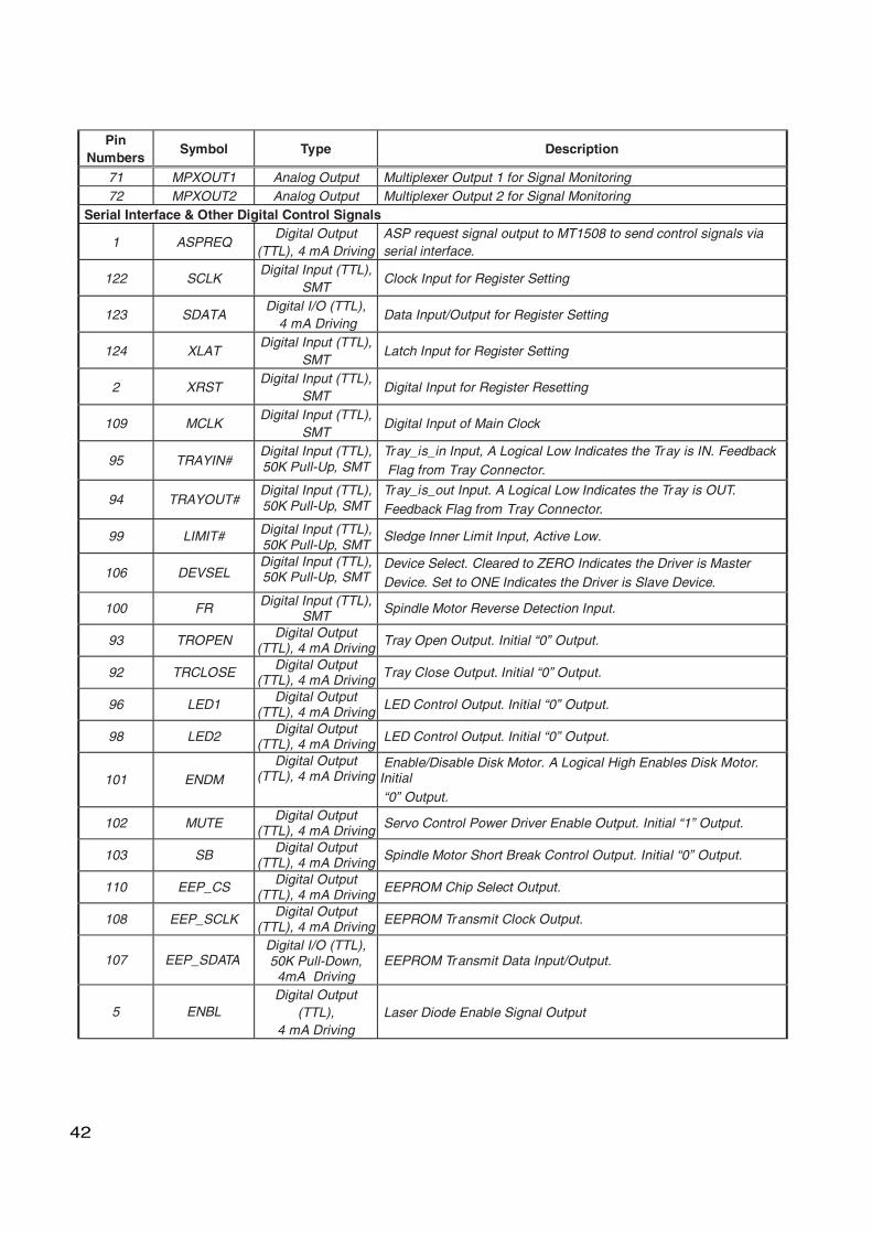
71 MPXOUT1 Analog Output Multiplexer Output 1 for Signal Monitoring 72 MPXOUT2 Analog Output Multiplexer Output 2 for Signal Monitoring
Serial Interface & Other Digital Control Signals
1 ASPREQ Digital Output
(TTL), 4 mA Driving ASP request signal output to MT1508 to send control signals via serial interface.
122 SCLK Digital Input (TTL),
SMT Clock Input for Register Setting
123 SDATA Digital I/O (TTL),
4 mA Driving Data Input/Output for Register Setting
124 XLAT Digital Input (TTL),
SMT Latch Input for Register Setting
2 XRST Digital Input (TTL),
SMT Digital Input for Register Resetting
109 MCLK Digital Input (TTL),
SMT Digital Input of Main Clock
95 TRAYIN# Digital Input (TTL), 50K Pull-Up, SMT
Tr n Input, A Logical Low Indicates the Tray is IN. Feedback Flag from Tray Connector.
94 TRAYOUT# Digital Input (TTL), 50K Pull-Up, SMT
Tr Input. A Logical Low Indicates the Tray is OUT. Feedback Flag from Tray Connector.
99 LIMIT# Digital Input (TTL), 50K Pull-Up, SMT
Sledge Inner Limit Input, Active Low.
106 DEVSEL Digital Input (TTL), 50K Pull-Up, SMT
Device Select. Cleared to ZERO Indicates the Driver is Master Device. Set to ONE Indicates the Driver is Slave Device.
100 FR Digital Input (TTL), SMT Spindle Motor Reverse Detection Input.
93 TROPEN Digital Output (TTL), 4 mA Driving Tray Open Output. Initial Output.
92 TRCLOSE Digital Output (TTL), 4 mA Driving Tray
96 LED1 Digital Output (TTL), 4 mA Driving LED Control Output. Initial Output.
98 LED2 Digital Output (TTL), 4 mA Driving LED Control Output. Initial Output.
101 ENDM Digital Output
(TTL), 4 mA Driving Enable/Disable Disk Motor. A Logical High Enables Disk Motor. Initial Output.
102 MUTE Digital Output (TTL), 4 mA Driving Servo Control Power Driver Enable Output. Initial Output.
103 SB Digital Output (TTL), 4 mA Driving Spindle Motor Short Break Control Output. Initial Output.
110 EEP_CS Digital Output (TTL), 4 mA Driving EEPROM Chip Select Output.
108 EEP_SCLK Digital Output (TTL), 4 mA Driving EEPROM Transmit Clock Output.
107 EEP_SDATA Digital I/O (TTL), 50K Pull-Down, 4mA Driving
EEPROM Transmit Data Input/Output.
5 ENBL Digital Output
(TTL), 4 mA Driving
Laser Diode Enable Signal Output

43
88 GIO1
Digital I/O (TTL), 50K Pull-Up, 4 mA Driving
(1). General I/O 1 for Mass Production Use (Initial Input Mode) (2). Output of Internal Digital Signal ( VWDC1 )
Pin Numbers
Symbol Type Description
89 GIO2 Digital I/O (TTL),
50K Pull-Up, 4 mA Driving
(1). General I/O 2 for Mass Production Use (Initial Input Mode) (2). Output of Defect Detection Signal ( DEFEC )
90 GIO3 Digital I/O (TTL), 50K Pull-Down, 4 mA Driving
(1). General I/O 3 for Mass Production Use (Initial Input Mode) (2). Output of the State of Seeking ON Control Setting
91 GIO4 Digital I/O (TTL), 50K Pull-Down, 4 mA Driving
(1). General I/O 4 for Mass Production Use (Initial Input Mode) (2). Output of Internal Digital Signal ( )
104 GIO5 Digital I/O (TTL),
50K Pull-Up, 4 mA Driving
(1). General I/O 5 for Mass Production Use (Initial Input Mode) (2). Output of Out-of-Track Detection Signal
105 GIO6 Digital I/O (TTL),
50K Pull-Up, 4 mA Driving
(1). General I/O 6 for Mass Production Use (Initial Input Mode) (2). Output of Out-of-Track Detection Signal ( XTOR )
119 GIO7 Digital I/O (TTL),
50K Pull-Up, 4 mA Driving
(1). General I/O 7 for Mass Production Use (Initial Input Mode) (2). Output of Recorded Area Detection Signal ( RECD1
Power Supplies 86 , 87 SUBGND Analog Ground Ground Pin for Substrate Bias of Internal Digital Circuitry
29 AVDD1 Analog Power Power Pin for Internal Analog Circuitry (5V) 35 AVSS1 Analog Ground Ground Pin for Internal Analog Circuitry 60 AVDD2 Analog Power Power Pin for Internal Analog Circuitry (5V) 64 AVSS2 Analog Ground Ground Pin for Internal Analog Circuitry 80 AVDD3 Analog Power Power Pin for Internal Analog Circuitry (5V) 84 AVSS3 Analog Ground Ground Pin for Internal Analog Circuitry 20 AVDD4 Analog Power Power Pin for Internal Analog Circuitry (5V) 18 AVSS4 Analog Ground Ground Pin for Internal Analog Circuitry 23 AVDD5 Analog Power Power Pin for Internal Analog Circuitry (5V) 25 AVSS5 Analog Ground Ground Pin for Internal Analog Circuitry 79 AVDD6 Analog Power Power Pin for Internal Analog Circuitry (5V) 73 AVSS6 Analog Ground Ground Pin for Internal Analog Circuitry 10 AVDD7 Analog Power Power Pin for Internal Analog Circuitry (5V)
6 , 7 AVSS7 Analog Ground Ground Pin for Internal Analog Circuitry 14 AVDD8 Analog Power Power Pin for Internal Analog Circuitry (5V) 12 AVSS8 Analog Ground Ground Pin for Internal Analog Circuitry 15 AVDD9 Analog Power Power Pin for Internal Analog Circuitry (5V) 17 AVSS9 Analog Ground Ground Pin for Internal Analog Circuitry
121 DVDD1 Digital Power Power Pin for Internal Digital Circuitry (5V) 117 DVSS1 Digital Ground Ground Pin for Internal Digital Circuitry 113 DVDD2 Digital Power Power Pin for Digital I/O Pads Buffer Circuitry (5V) 115 DVSS2 Digital Ground Ground Pin for Digital I/O Pads Buffer Circuitry

IC101(MT1508) : CD-R/RW Encoder/Decoder/Write Strategy / DSP /Interface /Micro Processor
Block Diagram
44
r
AD
GO
LOD
AC
VR
EF
RO
FOOTROFMO
PWMOUT
DM
AR
QIO
RDY
INTR
QIO
CS
16#
UP
3_7/
UR
D#
UA
LE
UP
3_6/
UW
R#
RA[11:0]RAS#CAS#CASH#/RWEH#RWE#ROE#CLKCKEDQMBA(1:0)
PRST#
PDMVDDPWM2VREF
PWMVREFPDMVSS
DA
CV
DD
DA
CV
SS
SRVADCVDDFEITEI
TEZILPTEI
HRFZC
RD[15:0]
UP
0[7:
0]/U
AD
[7:0
]
HR
ST
#D
IOW
#D
IOR
#D
MA
CK
#H
A[2
:0]
CS
1FX
#C
S3F
X#
HD
[15:
0]P
DIA
G#
DA
SP
#
TEST
8032Micro-controller
Key/LEDInterface
3KSRAM
EJECT#/STOP#PLAY#/PAUSE#
Host Interface
ATAPIPacketFIFO
HostDataFIFO
AudioDigital Out
CDROMHigh-speed
Audio Playback
ResetLogic
CDROMSync
DetectionDescrambler
CIRCError Corrector
RFZC/TEZCCircuit
PDM &PWM DAC
VaripitchCLV ClockGenerator
EFMDemodulator
SubcodeDemodulator
Servo DSP
UA
16/U
P1_
0
UP
SE
N#
UP
2_7~
UP
2_0
UA
[7:0
]
UP
3_5~
UP
3_4
UR
ST
UP
3_1~
UP
3_0
CLV/CAVController
Audio/EffectInterface
Audio DAC
PWM DAC
BufferMemory
Controller
ServoADC
C3Encoder
Sync.ProtectionData
PLL
DataSlicer
DPLLVDDIREF
LPFIN
DPLLVSSLPFIP
LPFON
LPIONLPFOP
LPIOP
DMO
FG
VPVDDVCOCINVPVSS
ENDM
C3Decoder
CIRC EncoderEFM modulatoin
Subcode generator
SystemClock
Generator
ASPControl
Interface
Write StrategyInterface
Logic
Servostatus
detectioncircuit
SC
OP
RFI
NR
FIP
RF
DT
SLV
NR
FD
TS
LVP
SC
ON
EFMPLL(efmclk
synthesizer)
SD
ATA
SD
EN
SLC
KX
RS
T#
WS
R_O
DO
N
WS
R_W
XR
WS
R_C
FR
EQ
FLA
G_O
UT
1F
LAG
_OU
T2
RLD
ON
SE
RV
SH
WB
LSH
WF
PD
SH
RF
PD
SH
WLD
ON
H11
T
Laser PowerControlLogic
OPC/ROPCComputation
Unit
Time toDigital
Converter
FLA
G_O
UT
1
FM Demodulator& Bi-Phase data
Demodulator
ATIP Sync Protection &CRC check &
Target MSF Search
WobbleSpindleControl
Wobble SignalInterface Logic
ATF
G
WB
LCLK
EF
MV
CO
IN
EF
MP
LLV
SS
EF
MP
LLV
DD
EF
MLP
FG
ND
XTALIIPLLVDDIPLLVSS
XTALO
systemclock
DMU
UP
3_2/
UN
IT0#
UP
3_3/
UIN
T1#
UA
17/U
P1_
1U
A18
/UP
1_2
FMO2
SRVADCVSS
CSISBAD

45
Pin Numbers Symbol Type Description
Data PLL Interface (9)
29 DPLLVDD Analog Power(3.3V)
Power supply for data PLL and related analog circuitry.
30 LPIOP Analog Output Data PLL VCO DAC positive output. 31 LPION Analog Output Data PLL VCO DAC negative output. 32 LPFOP Analog Output The positive output of loop filter amplifier. 33 LPFIN Analog Input The negative input terminal of loop filter amplifier. 34 LPFIP Analog Input The positive input terminal of loop filter amplifier. 35 LPFON Analog Output The negative output of loop filter amplifier. 36 IREF Analog Input Current reference input. It generates reference current for data
PLL. Connect an external 15K resistor between this pin and PLLVSS.
37 DPLLVSS Ground Ground pin for data PLL and related analog circuitry.
Signal Amplifier Interface (13)
38 SBAD Analog Input Sub-beam add input (E+F+G+H). 39 TEZILP Analog Input Tracking error zero crossing low pass input. 40 TEI Analog Input Tracki ng error input. 41 CSI Analog Input Central servo input. 42 FEI Analog Input Focus error input. 43 SRVADCVSS Ground Ground pin for servo ADC circuitry. 44 RFIN Analog Input RF negative signal input. 45 RFIP Analog Input RF positive signal input. 46 SRVADCVDD Analog
Power(3.3V) Power supply for servo ADC circuitry.
47 RFDTSLVN Analog Input Negative input for analog slicer. 48 SCOP Analog Output Positive low pass filter output for analog slicer. 49 SCON Analog Output Negative low pass filter output for analog slicer. 50 RFDTSLVP Analog Input Positive input for analog slicer.
Turbo 8032 Interface (37)
171 UP3_7 / URD#
3.3V LVTTL I/O, Slew rate, SMT,
4mA driving, 75K pull-up
Programmable bi-directional I/O. Alternate function : RD#. Data write signal.
172 UP3_6 / UWR#
3.3V LVTTL I/O, Slew rate, SMT,
4mA driving, 75K pull-up
Programmable bi-directional I/O. Alternate function : WR#. Data write signal.
173 UP3_3 / UINT1#
3.3V LVTTL I/O, Slew rate,
4mA driving, 75K pull-up
Programmable bi-directional I/O. Alternate function : INT1#. External interrupt 1.
174 UP3_2 / UINT0#
3.3V LVTTL I/O, Slew rate,
4mA driving, 75K pull-up
Programmable bi-directional I/O. Alternate function : INT0#. External interrupt 0.
• Pin Description

46
175 UP3_1 / UTXD
3.3V LVTTL I/O, Slew rate,
4mA driving, 75K pull-up
Programmable bi-directional I/O. Alternate function : TXD. Serial transmit data.
176 UP3_0 / URXD
3.3V LVTTL I/O, Slew rate,
4mA driving, 75K pull-up
Programmable bi-directional I/O. Alternate function : RXD. Serial receive data.
177 UALE 3.3V LVTTL I/O, Slew rate, SMT,
4mA driving, 75K pull-up
Address latch enable output during internal mode, active high. And as address latch enable input during ICE mode.
178 UPSEN# 3.3V LVTTL I/O, Slew rate, SMT,
4mA driving, 75K pull-up
Programmable store enable output during internal mode, active low. UPSEN# enables the external ROM output port. And as input during ICE mode.
189,188,186, 185,184,182,
181,179
UA[7:0] 3.3V LVTTL output, Slew rate,
2mA, 4mA, 6mA 8mA PDR, 75K pull-up
Lower address bus output for external device. Alternate function : Internal monitored signal output.
190,192,193, 194,195,197,
198,199
UP2_[7:0] / UA[15:8]
3.3V LVTTL output, Slew rate,
2mA, 4mA, 6mA 8mA PDR, 75K pull-up
Programmable bi-directional I/O. Alternate function : A[15:8]. Upper address bus input/output.
191 FLASH_WE# 3.3V LVTTL output, 4mA driving
Flash memory write enable signal output, low active.
200 UP1_1 /UA17
3.3V LVTTL output, Slew rate,
2mA, 4mA, 6mA 8mA PDR, 75K pull-up
Programmable bi-directional I/O. Alternate function : A17. Address bit 17 output.
201 UP1_0 / UA16
3.3V LVTTL output, Slew rate,
2mA, 4mA, 6mA 8mA PDR, 75K pull-up
Programmable bi-directional I/O. Alternate function : A16. Address bit 16 output.
202 FLASH_CS# 3.3V LVTTL I/O, Slew rate, SMT,
4mA driving, 75K pull-up
Flash memory chip select signal output, low active.
203,204,3, 4,5,6,8,9
UP0_[7:0] / UAD[7:0]
3.3V LVTTL output, Slew rate,
2mA, 4mA, 6mA 8mA PDR
Programmable bi-directional I/O. Alternate function : AD[7:0]. Lower address/data bus output for external device.
205 UP1_2 /UA18
3.3V LVTTL I/O, Slew rate,
4mA driving, 75K pull-up
Programmable bi-directional I/O. Alternate function : UA18. Address bit 18 output.
Motor and Actuator Driver Interface (11)

47
20 FG 3.3V LVTTL Input, SMT, 75K pull-up
Motor Hall sensor input. X
22 FOO Analog Output Focus servo output. PDM output of focus servo compensator. 23 TRO Analog Output Tracking servo output. PDM output of tracking servo
compensator. 24 PWMOUT Analog Output General purpose PWM output. 25 DMO Analog Output Disk motor control output. PWM output. 26 FMO Analog Output Feed motor control. PWM output. 27 FMO2 Analog Output Feed motor 2 control. PWM output. 51 PDMVDD Analog
Power(3.3V) Power supply for PDM circuitry.
52 2VREF Analog input 2.90 V reference voltage input. 53 VREF Analog input 1.45 V reference voltage input. 54 PDMVSS Ground Ground for PDM circuitry.
Mega Interface (2)
11 EJECT# 3.3V LVTTL I/O, 75K pull-up, 4mA driving
Eject/stop key input, active low. ZFA
12 PLAY# 3.3V LVTTL I/O, 75K pull-up, 4mA driving
Play/pause key input, active low. ZFA
Varipitch VCO Interface (3)
155 VPVSS Ground Ground pin for varipitch circuitry. 156 VPVCOCIN Analog Input Connect capacitor for compensator loop filter. 157 VPVDD Analog power(3.3V) Power supply for varipitch circuitry.
IPLL VCO Interface (2)
104 IPLLVDD Analog power(3.3V) Power supply for IPLL circuitry. 105 IPLLVSS Ground Ground pin for IPLL circuitry.
EFMPLL VCO Interface (4)
207 EFMPLLVDD Analog power(3.3V) Power supply for EFMPLL circuitry. 208 EFMVCOCIN Analog input EFMPLL VCO input. For external loop filter connection. 1 EFMLPFGND Analog input EFMPLL LPF ground input. 2 EFMPLLVSS Ground Ground pin for EFMPLL circuitry.
Audio Output Interface (1)
163 ADGO 3.3V LVTTL I/O, SMT, Slew rate,
75K pull-up, 4mA, 8mA driving
Digital Audio Output. The signal is the Digital Audio Output which supplies the IEC-958 digital audio data. Alternate function : HRST_ extension selection input during power-on stage (PRST falling edge). A logical low input indicates raw HRST_ is used. A logical high input indicates extended HRST_ is used.
ZFA
Internal Audio DAC Interface (5)
164 AUDACVSS Ground Ground pin for internal audio DAC circuitry. 165 LO Analog Output Left channel of audio. 166 DACVREF Analog Output Reference voltage for external audio filter circuit. 167 RO Analog Output Right channel of audio. 168 AUDACVDD Analog
Power(3.3V) Power supply for internal audio DAC circuitry.
48
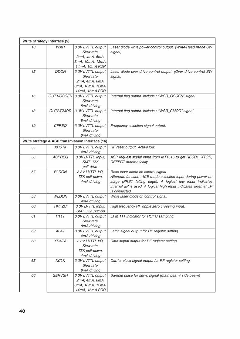
Write Strategy Interface (5)
13 WXR 3.3V LVTTL output, Slew rate,
2mA, 4mA, 6mA, 8mA, 10mA, 12mA, 14mA, 16mA PDR
Laser diode write power control output. (Write/Read mode SW signal)
15 ODON 3.3V LVTTL output, Slew rate,
2mA, 4mA, 6mA, 8mA, 10mA, 12mA, 14mA, 16mA PDR
Laser diode over drive control output. (Over drive control SW signal)
16 OUT1/OSCEN 3.3V LVTTL output, Slew rate,
8mA driving
Internal flag output. Include : WSR_OSCEN signal
18 OUT2/CMOD 3.3V LVTTL output, Slew rate,
8mA driving
Internal flag output. Include : WSR_CMOD signal
19 CFREQ 3.3V LVTTL output, Slew rate,
8mA driving
Frequency selection signal output.
Write strategy & ASP transmission Interface (16)
55 XRST# 3.3V LVTTL output, 4mA driving
RF reset output. Active low.
56 ASPREQ 3.3V LVTTL Input, SMT, 75K pull-down
ASP request signal input from MT1516 to get RECD1, XTOR, DEFECT automatically.
57 RLDON 3.3V LVTTL I/O, 75K pull-down,
4mA driving
Read laser diode on control signal. Alternate function : ICE mode selection input during power-on stage (PRST falling edge). A logical low input indicates internal is used. A logical high input indicates external is connected.
58 WLDON 3.3V LVTTL output, 4mA driving
Write laser diode on control signal.
60 HRFZC 3.3V LVTTL Input, SMT, 75K pull-up
High frequency RF ripple zero crossing input.
61 H11T 3.3V LVTTL output, Slew rate,
8mA driving
EFM 11T indicator for ROPC sampling.
62 XLAT 3.3V LVTTL output, 4mA driving
Latch signal output for RF register setting.
63 XDATA 3.3V LVTTL I/O, Slew rate,
75K pull-down, 4mA driving
Data signal output for RF register setting.
65 XCLK 3.3V LVTTL output, Slew rate,
8mA driving
Carrier clock signal output for RF register setting.
66 SERVSH 3.3V LVTTL output, 2mA, 4mA, 6mA,
8mA, 10mA, 12mA, 14mA, 16mA PDR
Sample pulse for servo signal (main beam/ side beam)

49
68 WBLSH 3.3V LVTTL output, 2mA, 4mA, 6mA,
8mA, 10mA, 12mA, 14mA, 16mA PDR
Sample pulse for wobble signal. YFA
69 ATFG 3.3V LVTTL Input, SMT
Digital wobble signal (22.05 1 K Hz) input X
70 WBLCLK 3.3V LVTTL output, Slew rate,
4mA driving
Wobble processing clock (432.18K Hz) output for MT1516. YFA
71 RFPDSH 3.3V LVTTL output, 2mA, 4mA, 6mA,
8mA, 10mA, 12mA, 14mA, 16mA PDR
Sample pulse control signal for RF read APC. YFA
72 WFPDSH 3.3V LVTTL output, Slew rate,
2mA, 4mA, 6mA, 8mA, 10mA, 12mA, 14mA, 16mA PDR
Sample pulse control signal for RF write APC. YFA
206 WRSTOP 3.3V LVTTL Input, SMT, 75K pull-down
Write procedure stop control input. X
Miscellaneous Interface (4)
169 TEST_MODE 3.3V LVTTL input Test mode, active high X170 PRST 3.3V LVTTL Input,
SMT Power on reset input, high active. X
74 XTALO Output X`tal output. 75 XTALI Input X`tal input. The working frequency is 33.8688 MHz.
Host Interface (31)
122 HRST# 3.3V LVTTL Input, SMT, 75K pull-up
Host reset input. The active-low input is referred to as hardware reset and is used to reset this chip.
X
142,140,138, 135,132,130, 127,124,123, 125,128,131, 133,136,139,
141
HD15 ~ HD0 3.3V LVTTL I/O, Slew rate, SMT,
4mA, 8mA, 12mA, 16mA PDR,
75K PPU, 75K PPD
Host Data bus. This is the 8-bit or 16-bit bi-directional data bus to the host. The lower 8 bits, HD0 D7, are used for 8-bit data transfers. Normally, data transfers are 16-bit wide. Note : All pins except HD7 (no any pull) may be selectively pull-up or pull-down with 20K resistant.
ZFA
144 DMARQ 3.3V LVTTL output, 12mA driving
DMA request. This signal is used for DMA data transfers between host and device and it shall be asserted by the MT1508 when it is ready to transfer data to or from the host. The direction of data transfer is controlled by DIOR# and DIOW#.
YFAtri
145 DIOW# 3.3V LVTTL Input, SMT, 75K pull-up
Device I/O write. Stop ultra DMA burst. For Device I/O Write, this signal is the strobe signal asserted by the host to write device register or the data port. For Stop Ultra DMA, this signal shall be negated by the host before data is transferred in an Ultra DMA burst and is asserted by host during an Ultra DMA burst to signal the termination of Ultra DMA burst.
X

50
146 DIOR# 3.3V LVTTL Input, SMT, 75K pull-up
Device I/O read. Ultra DMA ready. Ultra DMA data strobe. For Device I/O Read, this signal is the strobe signal asserted by the host to read device registers or the data port. For Ultra DMA ready, this is asserted by the host to indicate to the device that the host is ready to receive Ultra DMA data in burst to the host. For Ultra DMA data strobe, this signal is the data out strobe signal from the host for an Ultra DMA data out burst.
XF
148 IORDY 3.3V LVTTL I/O, SMT, Slew rate 16mA driving
I/O Channel Ready. Ultra DMA ready. Ultra DMA data strobe. For I/O channel Ready, this signal is negated to extend the host transfer cycle of any register read or write when the device is not able to complete the transfer. For Ultra DMA Ready, this signal is asserted by the device to indicate to the host that the device is ready to receive Ultra DMA data out bursts from the host. For Ultra DMA data strobe, this is the data in strobe signal from device for Ultra DMA data in burst to the host.
ZFA
149 DMACK# 3.3V LVTTL Input, SMT, 75K pull-up
DMA Acknowledge. This signal shall be used by the host in response to DMARQ to acknowledge that it is ready for DMA transfers.
XF
151 INTRQ 3.3V LVTTL I/O, Slew rate,
12mA driving
Device Interrupt. This signal is used to interrupt the host system. INTRQ is driven only when this chip is addressed. When not driven, INTRQ is in a high impedance state.
ZFA
152 IOCS16# 3.3V LVTTL output, 16mA driving
Device 16-BIT I/O. In PIO transfer modes 0, 1, and 2, IOCS16# indicates to the host system that the 16-bit data port has been addressed and that the device is prepared to send or receive a 16-bit data word.
YFA0
1 : tr
154 PDIAG# 3.3V LVTTL I/O, 12mA driving, 75K pull-up
Passed Diagnostics. This signal is asserted by Device 1 to indicate to Device 0 that it has completed diagnostics.
ZFA
159,153,158 HA2, HA0, HA1 3.3V LVTTL Input, SMT, 75K pull-up
Device Address. This is the 3-bit binary coded address pro-vided by the host to access an ATA register or data.
XF
160 CS1FX# 3.3V LVTTL Input, SMT, 75K pull-up
Device Chip Select 0 (for 1Fxh/17xh). This is the chip select signal from the host to select the Command Block Registers.
XF
161 CS3FX# 3.3V LVTTL Input, SMT, 75K pull-up
Device Chip Select 1 (for 3Fxh/37xh). This is the chip select signal from the host to select the Control Block Registers.
XF
162 DASP# 3.3V LVTTL I/O, 12mA driving, 75K pull-up
Device Active / Device 1 Present. This is a time-multiplexed signal that indicates that a device is active, or that Device 1 is present.
ZFA
Buffer Memory Interface (38)
82 BA1 3.3V LVTTL Output,
Slew rate, 2mA, 4mA, 6mA,
8mA, 10mA, 12mA, 14mA, 16mA PDR,
SDRAM bank address 1 signal. When 4-bank SDRAM is used, this pin is used to select bank2 and bank3 space and musts connect to pin of SDRAM. When two 2-bank SDRAM are used, this pin is used as Chip Select signal output for second SDRAM and musts connect to CS# pin of second SDRAM. When two DRAM are used, this pin is used as Row Address Strobe signal output for second DRAM and must connect to RAS# pin of second DRAM.
ZFA

51
84 BA0 3.3V LVTTL Output,
Slew rate, 2mA, 4mA, 6mA,
8mA, 10mA, 12mA, 14mA, 16mA PDR,
75K PPD
SDRAM bank address 0 signal. For SDRAM application only. ZFA2G
85 ROE# 3.3V LVTTL Output,
Slew rate, 2mA, 4mA, 6mA,
8mA, 10mA, 12mA, 14mA, 16mA PDR
RAM Output Enable, low active. For SDRAM application, this pin is “Chip Select” signal output connected to “CS#” pin of SDRAM. When two 2-bank SDRAM are used, this pin musts connect to “CS#” pin of first SDRAM.
ZFA2G
87 RAS# 3.3V LVTTL Output,
Slew rate, 2mA, 4mA, 6mA,
8mA, 10mA, 12mA, 14mA, 16mA PDR
RAM Row Address Strobe. This active-low output is the Row Address Strobe signal to the RAM. For SDRAM application, this pin is “row address strobe” signal output connected to SDRAM.
ZFA2G
88 CAS# 3.3V LVTTL Output,
Slew rate, 2mA, 4mA, 6mA,
8mA, 10mA, 12mA, 14mA, 16mA PDR
Column Address Strobe Low / Column Address Strobe. When two column address strobe pins are used, this pin is the Column Address Strobe Low signal for accessing the lower bytes of a two-CAS# 16-bit RAM. When an 8-bit DRAM is used, this pin shall be connected to CAS# of the DRAM. For SDRAM application, this pin is “column address strobe” signal output connected to SDRAM.
ZFA2G
89 RWE# 3.3V LVTTL Output,
Slew rate, 2mA, 4mA, 6mA,
8mA, 10mA, 12mA, 14mA, 16mA PDR
RAM Write Enable/RAM Write Enable Low. RAM write enable signal, low active. When two write enable pins are used, it is the Write Enable Low signal for writing the lower bytes of a two-WE_ 16-bit RAM. For SDRAM application, this pin is dedicated for “Write Enable” usage.
ZFA2G
90 DQML 3.3V LVTTL Output,
Slew rate, 2mA, 4mA, 6mA,
8mA, 10mA, 12mA, 14mA, 16mA PDR,
75K PPD
SDRAM low-byte data output mask control signal, high active. For SDRAM application only.
ZFA2G
116 CASH#/
RWEH#
3.3V LVTTL Output,
Slew rate, 2mA, 4mA, 6mA,
8mA, 10mA, 12mA, 14mA, 16mA PDR
Column Address Strobe High / RAM Write Enable High. When a 16-bit DRAM is used, this active-low pin functions as Column address Strobe High for accessing the upper bytes of a two-CAS# RAM, or as Write Enable High for writing the upper bytes of a two-WE# RAM. For SDRAM application, this pin is changed to DQMH and is used to as SDRAM high-byte data mask control signal, high active.
ZFA2G

52
117 CLK 3.3V LVTTL Output,
Slew rate, 2mA, 4mA, 6mA,
8mA, 10mA, 12mA, 14mA, 16mA PDR,
75K PPD
SDRAM clock output. For SDRAM application only. ZFA2
118 CKE 3.3V LVTTL Output,
Slew rate, 2mA, 4mA, 6mA,
8mA, 10mA, 12mA, 14mA, 16mA PDR,
75K PPD
SDRAM clock enable signal output. For SDRAM application only.
ZFA2
106,107,108, 109,110,112, 113,115,92, 93,94,95,96,
97,98,99
RD15 ~ RD0 3.3V LVTTL I/O, Slew rate,
2mA, 4mA, 6mA, 8mA, 10mA, 12mA, 14mA, 16mA PDR, 75K PPU, 75K PPD
RAM Data bus. These pins are the bi-directional upper Buffer RAM data bus to the external buffer memory.
ZFA2
119,81,120, 121,103,102.
101,100,77,78, 79,80
RA11~ RA0 3.3V LVTTL Output,
Slew rate, 2mA, 4mA, 6mA,
8mA, 10mA, 12mA, 14mA, 16mA PDR
RAM address bus. ZFA2
Power Supply (27)
91,143,196 (3) DVDD33 Power (3.3V) Power supply for input pad buffer circuitry. 17,76,134,180
(4) DVDD25 Power (2.5V) Power supply for internal digital circuitry and general pad
buffer circuitry. 14,73,137,183
(4) DVSS Ground Ground pin for internal digital circuitry and input pad buffer
circuitry. 7,67,86,111, 129,150 (6)
DVDD33 Power (3.3V) Power supply for output pad buffer circuitry.
10,64,83,114, 126,147,187 (7)
DVSS Ground Ground pin for output pad buffer circuitry.
28 AVDD25 Power (2.5V) Power supply for dedicated digital circuitry in fully block. 21 AVSS Ground Ground pin for dedicated digital circuitry in fully block. 59 AVDD33 Power (3.3V) Power supply for dedicated digital circuitry in fully block.

53
IC501 (BD7907FS): Spindle Motor and 5ch Actuator Driver
Block Diagram
LEV
EL
SH
IFT
LEV
EL
SH
IFT
HA
LLB
IAS
FG
RE
VE
RC
ED
ET
EC
T
TS
D
PR
ELO
GIC
Current
LIMIT
PR
ELO
GIC
LEV
EL
SH
IFT
47K
47K
94K94K
47K
47K
47K
47K
47K
94K
FF
FF
FF
OS
C
OS
C
3-phaseM
AT
RIX
Current
CO
MPPolarity
CO
MP
PW
MO
UT
FG
LIMIT
LIMIT
15K15K
ST
BY
/B
RA
KE
CO
NT
RO
L
541 DVCCHU+
2HU-
3HV+
4HV-
5HW+
6HW-
7HB
8PGND1
9U
10SPVM1
11V
12GND
13GND
14GND
15GND
16GND
17PGND2
18W
19SPVM2
20SPRNF
21FG
22CTL1
23CTL2
24SPIN
25DGND
26LDIN
27VC
53 FCIN
52 TKIN
51 VCC
50 LDO+
49 LDO-
48 TKO+
47 TKO-
46 FCO+
45 FCO-
44 AVM
43 GND
42 GND
41 GND
40 GND
39 GND
38 AGND
37 SLO1+
36 SLO1-
35 SLO2+
34 SLO2-
33 SLGND
32 SLRNF2
31 SLRNF1
30 SLVDD
29 SLIN2
28 SLIN1
54
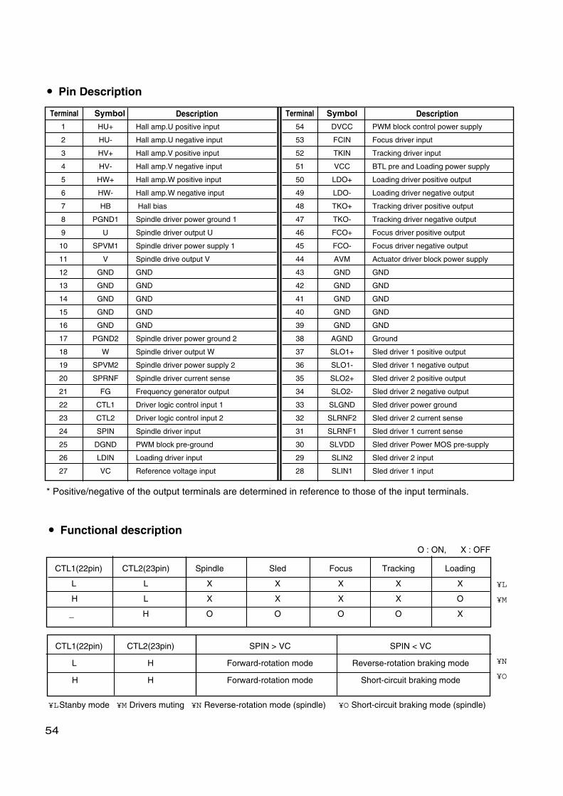
• Pin Description
Terminal Symbol Description1 HU+ Hall amp.U positive input
2 HU- Hall amp.U negative input
3 HV+ Hall amp.V positive input
4 HV- Hall amp.V negative input
5 HW+ Hall amp.W positive input
6 HW- Hall amp.W negative input
7 HB Hall bias
8 PGND1 Spindle driver power ground 1
9 U Spindle driver output U
10 SPVM1 Spindle driver power supply 1
11 V Spindle drive output V
12 GND GND
13 GND GND
14 GND GND
15 GND GND
16 GND GND
17 PGND2 Spindle driver power ground 2
18 W Spindle driver output W
19 SPVM2 Spindle driver power supply 2
20 SPRNF Spindle driver current sense
21 FG Frequency generator output
22 CTL1 Driver logic control input 1
23 CTL2 Driver logic control input 2
24 SPIN Spindle driver input
25 DGND PWM block pre-ground
26 LDIN Loading driver input
27 VC Reference voltage input
Terminal Symbol Description54 DVCC PWM block control power supply
53 FCIN Focus driver input
52 TKIN Tracking driver input
51 VCC BTL pre and Loading power supply
50 LDO+ Loading driver positive output
49 LDO- Loading driver negative output
48 TKO+ Tracking driver positive output
47 TKO- Tracking driver negative output
46 FCO+ Focus driver positive output
45 FCO- Focus driver negative output
44 AVM Actuator driver block power supply
43 GND GND
42 GND GND
41 GND GND
40 GND GND
39 GND GND
38 AGND Ground
37 SLO1+ Sled driver 1 positive output
36 SLO1- Sled driver 1 negative output
35 SLO2+ Sled driver 2 positive output
34 SLO2- Sled driver 2 negative output
33 SLGND Sled driver power ground
32 SLRNF2 Sled driver 2 current sense
31 SLRNF1 Sled driver 1 current sense
30 SLVDD Sled driver Power MOS pre-supply
29 SLIN2 Sled driver 2 input
28 SLIN1 Sled driver 1 input
* Positive/negative of the output terminals are determined in reference to those of the input terminals.
• Functional description
CTL1(22pin) CTL2(23pin) Spindle Sled Focus Tracking Loading
L L X X X X X
H L X X X X O
_ H O O O O X
CTL1(22pin) CTL2(23pin) SPIN > VC SPIN < VC
L H Forward-rotation mode Reverse-rotation braking mode
H H Forward-rotation mode Short-circuit braking mode
O : ON, X : OFF
¥L
¥M
¥N
¥O
¥LStanby mode ¥M Drivers muting ¥N Reverse-rotation mode (spindle) ¥O Short-circuit braking mode (spindle)

033
PBM00 (MAIN C.B.A)
007
A02
A01
020
028029
030
400
032
400
021
020050
413413
413
001
413430
012
009
008013
014
005035
016
015
004
006
A B C D E F G H
1
2
3
4
5
017
003
002
010
011
030
400400
031
027026034
025
430419
021
400
11 12
EXPLODED VIEW
Copyright © 2022 FDOKUMEN


![Phonetic features and phonological features, by Theo Vennemann and Peter Ladefoged [1973]](https://static.fdokumen.com/doc/165x107/631b5827a906b217b9066a9d/phonetic-features-and-phonological-features-by-theo-vennemann-and-peter-ladefoged.jpg)