CHE 320: Organic Spectroscopy NMR Lecture Notes 2 Introduction to NMR
Upload
khangminh22Category
view
1download
0
UNIVERS ITE IT •STELLENBOSCH •UNIVERS ITY
j ou kenn i s v ennoo t • you r know ledge pa r tne r
Integrated, FPGA Based
NMR Teslameter and Power Supply for
Accelerator Magnets
by
John-Philip Taylor
Thesis presentedin partial fulfilment of the requirements for the degree of
Master of Science in Engineering(Electronic Engineering with Computer Science)
at the
University of Stellenbosch
Department of Electrical and Electronic Engineering,University of Stellenbosch,
Private Bag X1, 7602 Matieland, South Africa.
Supervisor: Prof H du T MoutonCo-Supervisor: Prof T Jones
March 2007

Copyright © 2007 University of StellenboschAll rights reserved.
Declaration
I, the undersigned, hereby declare that the work contained in this thesis is my own originalwork and that I have not previously in its entirety or in part submitted it at any universityfor a degree.
Signature: . . . . . . . . . . . . . . . . . . . . . . . . . . . . . . . . . .J Taylor
Date: . . . . . . . . . . . . . . . . . . . . . . . . . . . . . . . . . . . . . . .
ii

Abstract
Particle accelerators today have numerous magnets that require controlling. These includemagnets for analysing, beam-path selection, focusing, etc. Also, design specifications arebecoming tighter. A typical modern magnet power supply is expected to have a resolutionof 16-bit and a stability of 10 ppm.
This thesis addresses two research areas. First, various aspects of high-performanceaccelerator magnet power supplies are investigated. An isolated dual-stage 3.5 kW converteris designed. The concept is verified through practical measurements. The control systemand high-resolution pulse-width modulation are implemented within a field-programmablegate array.
Second, a nuclear-magnetic resonance probe is designed and simulated. It is intended toprovide a measurement of field-strength for feed-back purposes. Some adjustments are madewith existing technology in order to decrease the time between successive measurements tothe order of 10 µs.
Also, the support systems (central processing unit, hardware drivers, etc.) are designed,implemented in the field-programmable gate array and tested successfully.
iii

Opsomming
Hedendaagse partikel versnellers beskik oor talle magnete wat beheer verg. Hierdie sluitin magnete vir analise, straal-pad seleksie, fokus ens. Stelsel spesifikasies raak boonoptoenemend knellend. ’n Tipiese moderne magneet kragbron is veronderstel om 16-bisresolusie en 10 ppm stabiliteit te waarborg.
Hierdie tesis adresseer twee navorsings areas: Eerstens word verskeie aspekte van hoewerkverrigting versnellersmagneet kragbronne ondersoek. ’n Geısoleerde dubbel stadium3.5 kW omsetter is ontwerp. Die beginsel is bevestig deur middel van praktiese metings.Die beheerstelsel en hoe-resolusie pulswydte modulator word geımplementeer deur middelvan ’n veld-programmeerbare hekskikking (FPGA).
Tweedens, ’n kernmagnetiese resonansie probe is ontwerp en gesimuleer. Dit is bestemom ’n meting van veldsterkte te voorsien vir terugvoer doeleindes. Sommige verstellings isgemaak aan bestaande tegnologie ten einde die tydsverloop tussen opeenvolgende metingste verminder tot die orde van 10 µs.
Laastens, die ondersteuningstelsels (mikroverwerker, hardeware drywers ens.) is ontwerp,geımplementeer in die FPGA en suksesvol getoets.
iv

Acknowledgement
I would like to thank the following people:
• Prof H du T Mouton and Prof T Jones for their guidance as supervisors
• Dr C B Franklyn at NECSA for providing the idea, as well as funding, for this project
• Sandi Swanepoel, my fiance, for proofreading and grammatical checks, as well as allthe love and support in the world
• My fellow colleagues for being so supportive and available to exchange problems andideas
• All the lecturers along my path from whom I have learnt the basics needed in orderto complete this thesis
• Last but not least, my parents for enabling me to develop my full potential and pursuemy dreams
v
Contents
Declaration ii
Abstract iii
Opsomming iv
Acknowledgement v
Contents vi
List of Figures xv
List of Tables xix
Nomenclature xxi
1 Introduction 11.1 Background . . . . . . . . . . . . . . . . . . . . . . . . . . . . . . . . . . . . . 11.2 Research Objectives . . . . . . . . . . . . . . . . . . . . . . . . . . . . . . . . 21.3 Thesis Overview . . . . . . . . . . . . . . . . . . . . . . . . . . . . . . . . . . 3
2 Existing Technology 42.1 Introduction . . . . . . . . . . . . . . . . . . . . . . . . . . . . . . . . . . . . . 42.2 Existing System . . . . . . . . . . . . . . . . . . . . . . . . . . . . . . . . . . . 4
2.2.1 Analysing Magnet . . . . . . . . . . . . . . . . . . . . . . . . . . . . . 52.2.2 Current Source . . . . . . . . . . . . . . . . . . . . . . . . . . . . . . . 72.2.3 Probe . . . . . . . . . . . . . . . . . . . . . . . . . . . . . . . . . . . . 82.2.4 Controller . . . . . . . . . . . . . . . . . . . . . . . . . . . . . . . . . . 9
2.3 Products on the Market . . . . . . . . . . . . . . . . . . . . . . . . . . . . . . 102.3.1 Digital Teslameter . . . . . . . . . . . . . . . . . . . . . . . . . . . . . 102.3.2 Current Source . . . . . . . . . . . . . . . . . . . . . . . . . . . . . . . 10
2.4 High Performance Magnet Power Supplies . . . . . . . . . . . . . . . . . . . . 102.4.1 Topologies . . . . . . . . . . . . . . . . . . . . . . . . . . . . . . . . . . 112.4.2 Feed Forward Techniques . . . . . . . . . . . . . . . . . . . . . . . . . 122.4.3 Digital Control . . . . . . . . . . . . . . . . . . . . . . . . . . . . . . . 13
2.5 Field Measurement Techniques . . . . . . . . . . . . . . . . . . . . . . . . . . 132.5.1 Calibrated Current Measurement . . . . . . . . . . . . . . . . . . . . . 132.5.2 Calibrated Hall Effect Probe . . . . . . . . . . . . . . . . . . . . . . . 142.5.3 Continuous Wave NMR . . . . . . . . . . . . . . . . . . . . . . . . . . 142.5.4 Pulsed NMR . . . . . . . . . . . . . . . . . . . . . . . . . . . . . . . . 14
2.6 Summary . . . . . . . . . . . . . . . . . . . . . . . . . . . . . . . . . . . . . . 15
vi

CONTENTS vii
3 Design Overview 163.1 Introduction . . . . . . . . . . . . . . . . . . . . . . . . . . . . . . . . . . . . . 163.2 Block Diagrams . . . . . . . . . . . . . . . . . . . . . . . . . . . . . . . . . . . 16
3.2.1 General Block Diagram . . . . . . . . . . . . . . . . . . . . . . . . . . 163.2.2 Mains and Power Supply . . . . . . . . . . . . . . . . . . . . . . . . . 173.2.3 Power Converter . . . . . . . . . . . . . . . . . . . . . . . . . . . . . . 183.2.4 Probe . . . . . . . . . . . . . . . . . . . . . . . . . . . . . . . . . . . . 183.2.5 Controller . . . . . . . . . . . . . . . . . . . . . . . . . . . . . . . . . . 19
3.3 Overall Layout . . . . . . . . . . . . . . . . . . . . . . . . . . . . . . . . . . . 203.3.1 Front Panel . . . . . . . . . . . . . . . . . . . . . . . . . . . . . . . . . 203.3.2 Layout . . . . . . . . . . . . . . . . . . . . . . . . . . . . . . . . . . . . 20
3.4 Summary . . . . . . . . . . . . . . . . . . . . . . . . . . . . . . . . . . . . . . 21
4 Converter 234.1 Introduction . . . . . . . . . . . . . . . . . . . . . . . . . . . . . . . . . . . . . 234.2 Definitions . . . . . . . . . . . . . . . . . . . . . . . . . . . . . . . . . . . . . . 234.3 Specification . . . . . . . . . . . . . . . . . . . . . . . . . . . . . . . . . . . . . 24
4.3.1 Source of Power . . . . . . . . . . . . . . . . . . . . . . . . . . . . . . 244.3.2 Power Rating and Load . . . . . . . . . . . . . . . . . . . . . . . . . . 244.3.3 Isolation . . . . . . . . . . . . . . . . . . . . . . . . . . . . . . . . . . . 244.3.4 Range . . . . . . . . . . . . . . . . . . . . . . . . . . . . . . . . . . . . 244.3.5 Stability . . . . . . . . . . . . . . . . . . . . . . . . . . . . . . . . . . . 254.3.6 Audible Noise . . . . . . . . . . . . . . . . . . . . . . . . . . . . . . . . 25
4.4 Topology . . . . . . . . . . . . . . . . . . . . . . . . . . . . . . . . . . . . . . 254.4.1 Overall . . . . . . . . . . . . . . . . . . . . . . . . . . . . . . . . . . . 254.4.2 Rectifier . . . . . . . . . . . . . . . . . . . . . . . . . . . . . . . . . . . 264.4.3 Stage 1 . . . . . . . . . . . . . . . . . . . . . . . . . . . . . . . . . . . 274.4.4 Stage 2 . . . . . . . . . . . . . . . . . . . . . . . . . . . . . . . . . . . 29
4.5 Rectifier Detail . . . . . . . . . . . . . . . . . . . . . . . . . . . . . . . . . . . 304.5.1 Bus Capacitor . . . . . . . . . . . . . . . . . . . . . . . . . . . . . . . 304.5.2 Waveforms . . . . . . . . . . . . . . . . . . . . . . . . . . . . . . . . . 314.5.3 Line-Frequency Ripple . . . . . . . . . . . . . . . . . . . . . . . . . . . 324.5.4 Ripple Current Through Bus Capacitor . . . . . . . . . . . . . . . . . 334.5.5 Losses . . . . . . . . . . . . . . . . . . . . . . . . . . . . . . . . . . . . 334.5.6 Supply Current . . . . . . . . . . . . . . . . . . . . . . . . . . . . . . . 33
4.6 Stage 1 Detail . . . . . . . . . . . . . . . . . . . . . . . . . . . . . . . . . . . . 344.6.1 Switches . . . . . . . . . . . . . . . . . . . . . . . . . . . . . . . . . . . 344.6.2 Switching . . . . . . . . . . . . . . . . . . . . . . . . . . . . . . . . . . 344.6.3 Waveforms . . . . . . . . . . . . . . . . . . . . . . . . . . . . . . . . . 354.6.4 Transformer Winding Ratio . . . . . . . . . . . . . . . . . . . . . . . . 374.6.5 High Frequency Rectifier . . . . . . . . . . . . . . . . . . . . . . . . . 374.6.6 Switching Frequency . . . . . . . . . . . . . . . . . . . . . . . . . . . . 384.6.7 Filter . . . . . . . . . . . . . . . . . . . . . . . . . . . . . . . . . . . . 384.6.8 Losses . . . . . . . . . . . . . . . . . . . . . . . . . . . . . . . . . . . . 404.6.9 Dead Time . . . . . . . . . . . . . . . . . . . . . . . . . . . . . . . . . 41
4.7 Transformer Detail . . . . . . . . . . . . . . . . . . . . . . . . . . . . . . . . . 424.7.1 Configuration . . . . . . . . . . . . . . . . . . . . . . . . . . . . . . . . 424.7.2 Non-Ideal Properties . . . . . . . . . . . . . . . . . . . . . . . . . . . . 434.7.3 Leakage Inductance . . . . . . . . . . . . . . . . . . . . . . . . . . . . 444.7.4 Isolation . . . . . . . . . . . . . . . . . . . . . . . . . . . . . . . . . . . 444.7.5 Thermal Analysis . . . . . . . . . . . . . . . . . . . . . . . . . . . . . . 46
4.8 Stage 2 Detail . . . . . . . . . . . . . . . . . . . . . . . . . . . . . . . . . . . . 47
CONTENTS viii
4.8.1 Switches . . . . . . . . . . . . . . . . . . . . . . . . . . . . . . . . . . . 474.8.2 Switching . . . . . . . . . . . . . . . . . . . . . . . . . . . . . . . . . . 474.8.3 Waveforms . . . . . . . . . . . . . . . . . . . . . . . . . . . . . . . . . 474.8.4 Switching Frequency . . . . . . . . . . . . . . . . . . . . . . . . . . . . 494.8.5 Filter . . . . . . . . . . . . . . . . . . . . . . . . . . . . . . . . . . . . 494.8.6 Losses . . . . . . . . . . . . . . . . . . . . . . . . . . . . . . . . . . . . 504.8.7 Dead Time . . . . . . . . . . . . . . . . . . . . . . . . . . . . . . . . . 51
4.9 Heatsink . . . . . . . . . . . . . . . . . . . . . . . . . . . . . . . . . . . . . . . 514.9.1 Contribution of Stage 1 MOSFETS . . . . . . . . . . . . . . . . . . . . 514.9.2 Contribution of Stage 1 Diodes . . . . . . . . . . . . . . . . . . . . . . 524.9.3 Contribution of Stage 2 MOSFETS . . . . . . . . . . . . . . . . . . . . 524.9.4 The Required Heatsink . . . . . . . . . . . . . . . . . . . . . . . . . . 52
4.10 Physical Layout . . . . . . . . . . . . . . . . . . . . . . . . . . . . . . . . . . . 534.11 Summary . . . . . . . . . . . . . . . . . . . . . . . . . . . . . . . . . . . . . . 54
5 Control System 555.1 Introduction . . . . . . . . . . . . . . . . . . . . . . . . . . . . . . . . . . . . . 555.2 Specification . . . . . . . . . . . . . . . . . . . . . . . . . . . . . . . . . . . . . 55
5.2.1 Range . . . . . . . . . . . . . . . . . . . . . . . . . . . . . . . . . . . . 555.2.2 Bandwidth . . . . . . . . . . . . . . . . . . . . . . . . . . . . . . . . . 555.2.3 Accuracy . . . . . . . . . . . . . . . . . . . . . . . . . . . . . . . . . . 565.2.4 Stability . . . . . . . . . . . . . . . . . . . . . . . . . . . . . . . . . . . 565.2.5 Resolution . . . . . . . . . . . . . . . . . . . . . . . . . . . . . . . . . . 56
5.3 Block Diagrams . . . . . . . . . . . . . . . . . . . . . . . . . . . . . . . . . . . 575.3.1 System Diagram . . . . . . . . . . . . . . . . . . . . . . . . . . . . . . 575.3.2 Stage 1 . . . . . . . . . . . . . . . . . . . . . . . . . . . . . . . . . . . 575.3.3 Stage 2 . . . . . . . . . . . . . . . . . . . . . . . . . . . . . . . . . . . 595.3.4 Estimator . . . . . . . . . . . . . . . . . . . . . . . . . . . . . . . . . . 605.3.5 Feed-Forward . . . . . . . . . . . . . . . . . . . . . . . . . . . . . . . . 61
5.4 System Models . . . . . . . . . . . . . . . . . . . . . . . . . . . . . . . . . . . 615.4.1 Stage 1 . . . . . . . . . . . . . . . . . . . . . . . . . . . . . . . . . . . 615.4.2 Stage 2 . . . . . . . . . . . . . . . . . . . . . . . . . . . . . . . . . . . 645.4.3 Integrator . . . . . . . . . . . . . . . . . . . . . . . . . . . . . . . . . . 65
5.5 Pole Placement . . . . . . . . . . . . . . . . . . . . . . . . . . . . . . . . . . . 655.5.1 Stage 1 . . . . . . . . . . . . . . . . . . . . . . . . . . . . . . . . . . . 655.5.2 Stage 2 . . . . . . . . . . . . . . . . . . . . . . . . . . . . . . . . . . . 68
5.6 Measurements . . . . . . . . . . . . . . . . . . . . . . . . . . . . . . . . . . . . 705.6.1 Analogue vs Digital . . . . . . . . . . . . . . . . . . . . . . . . . . . . 705.6.2 Resolution . . . . . . . . . . . . . . . . . . . . . . . . . . . . . . . . . . 705.6.3 Actual Measurements . . . . . . . . . . . . . . . . . . . . . . . . . . . 715.6.4 Estimated . . . . . . . . . . . . . . . . . . . . . . . . . . . . . . . . . . 735.6.5 Noise . . . . . . . . . . . . . . . . . . . . . . . . . . . . . . . . . . . . 735.6.6 Other . . . . . . . . . . . . . . . . . . . . . . . . . . . . . . . . . . . . 75
5.7 Simulation . . . . . . . . . . . . . . . . . . . . . . . . . . . . . . . . . . . . . . 755.7.1 Stage 1 . . . . . . . . . . . . . . . . . . . . . . . . . . . . . . . . . . . 755.7.2 Stage 2 . . . . . . . . . . . . . . . . . . . . . . . . . . . . . . . . . . . 765.7.3 Combined . . . . . . . . . . . . . . . . . . . . . . . . . . . . . . . . . . 80
5.8 Soft-Start . . . . . . . . . . . . . . . . . . . . . . . . . . . . . . . . . . . . . . 825.8.1 Rectifier . . . . . . . . . . . . . . . . . . . . . . . . . . . . . . . . . . . 825.8.2 Converter . . . . . . . . . . . . . . . . . . . . . . . . . . . . . . . . . . 83
5.9 Firmware Implementation . . . . . . . . . . . . . . . . . . . . . . . . . . . . . 835.9.1 Digital Representation . . . . . . . . . . . . . . . . . . . . . . . . . . . 83
CONTENTS ix
5.9.2 Time-Step . . . . . . . . . . . . . . . . . . . . . . . . . . . . . . . . . . 865.9.3 Reciprocal . . . . . . . . . . . . . . . . . . . . . . . . . . . . . . . . . . 865.9.4 Smoother . . . . . . . . . . . . . . . . . . . . . . . . . . . . . . . . . . 875.9.5 Soft-Start . . . . . . . . . . . . . . . . . . . . . . . . . . . . . . . . . . 885.9.6 Timing . . . . . . . . . . . . . . . . . . . . . . . . . . . . . . . . . . . 885.9.7 Protection . . . . . . . . . . . . . . . . . . . . . . . . . . . . . . . . . . 89
5.10 Summary . . . . . . . . . . . . . . . . . . . . . . . . . . . . . . . . . . . . . . 89
6 Digital PWM 916.1 Introduction . . . . . . . . . . . . . . . . . . . . . . . . . . . . . . . . . . . . . 916.2 Resolution . . . . . . . . . . . . . . . . . . . . . . . . . . . . . . . . . . . . . . 91
6.2.1 Required Resolution . . . . . . . . . . . . . . . . . . . . . . . . . . . . 916.2.2 Practical Digital PWM . . . . . . . . . . . . . . . . . . . . . . . . . . 926.2.3 Delay-Line . . . . . . . . . . . . . . . . . . . . . . . . . . . . . . . . . 92
6.3 Noise-Shaper . . . . . . . . . . . . . . . . . . . . . . . . . . . . . . . . . . . . 946.3.1 Quantisation as a Noise Source . . . . . . . . . . . . . . . . . . . . . . 946.3.2 Block Diagram . . . . . . . . . . . . . . . . . . . . . . . . . . . . . . . 946.3.3 Theory of Operation . . . . . . . . . . . . . . . . . . . . . . . . . . . . 956.3.4 Implementation . . . . . . . . . . . . . . . . . . . . . . . . . . . . . . . 966.3.5 Performance . . . . . . . . . . . . . . . . . . . . . . . . . . . . . . . . 97
6.4 PWM Generator . . . . . . . . . . . . . . . . . . . . . . . . . . . . . . . . . . 996.4.1 Stage 1 . . . . . . . . . . . . . . . . . . . . . . . . . . . . . . . . . . . 996.4.2 Stage 2 . . . . . . . . . . . . . . . . . . . . . . . . . . . . . . . . . . . 100
6.5 Summary . . . . . . . . . . . . . . . . . . . . . . . . . . . . . . . . . . . . . . 100
7 Probe 1017.1 Introduction . . . . . . . . . . . . . . . . . . . . . . . . . . . . . . . . . . . . . 1017.2 Phase-Locked Loop NMR . . . . . . . . . . . . . . . . . . . . . . . . . . . . . 101
7.2.1 Principle of Operation . . . . . . . . . . . . . . . . . . . . . . . . . . . 1017.2.2 Phase-Locked Loop . . . . . . . . . . . . . . . . . . . . . . . . . . . . . 1027.2.3 Sustaining Resonance . . . . . . . . . . . . . . . . . . . . . . . . . . . 1037.2.4 Simulation . . . . . . . . . . . . . . . . . . . . . . . . . . . . . . . . . 105
7.3 Hardware Detail . . . . . . . . . . . . . . . . . . . . . . . . . . . . . . . . . . 1097.3.1 Modified Bloch Equations . . . . . . . . . . . . . . . . . . . . . . . . . 1097.3.2 Excitation Coil . . . . . . . . . . . . . . . . . . . . . . . . . . . . . . . 1107.3.3 Detection Coil . . . . . . . . . . . . . . . . . . . . . . . . . . . . . . . 1107.3.4 Using a Single Coil . . . . . . . . . . . . . . . . . . . . . . . . . . . . . 1117.3.5 Measurement Technique . . . . . . . . . . . . . . . . . . . . . . . . . . 1117.3.6 Parasitic Components . . . . . . . . . . . . . . . . . . . . . . . . . . . 113
7.4 Alternative Control Circuit . . . . . . . . . . . . . . . . . . . . . . . . . . . . 1157.4.1 DDS Operation . . . . . . . . . . . . . . . . . . . . . . . . . . . . . . . 1157.4.2 Frequency Content . . . . . . . . . . . . . . . . . . . . . . . . . . . . . 1167.4.3 Block Diagram . . . . . . . . . . . . . . . . . . . . . . . . . . . . . . . 116
7.5 Summary . . . . . . . . . . . . . . . . . . . . . . . . . . . . . . . . . . . . . . 117
8 Controller 1198.1 Introduction . . . . . . . . . . . . . . . . . . . . . . . . . . . . . . . . . . . . . 1198.2 Hardware . . . . . . . . . . . . . . . . . . . . . . . . . . . . . . . . . . . . . . 119
8.2.1 Block Diagram . . . . . . . . . . . . . . . . . . . . . . . . . . . . . . . 1198.2.2 Central Processor . . . . . . . . . . . . . . . . . . . . . . . . . . . . . . 1208.2.3 Power Supply . . . . . . . . . . . . . . . . . . . . . . . . . . . . . . . . 1208.2.4 Start-Up Sequence . . . . . . . . . . . . . . . . . . . . . . . . . . . . . 122
CONTENTS x
8.2.5 Programmer . . . . . . . . . . . . . . . . . . . . . . . . . . . . . . . . 1228.2.6 Interface Headers . . . . . . . . . . . . . . . . . . . . . . . . . . . . . . 1228.2.7 ADC . . . . . . . . . . . . . . . . . . . . . . . . . . . . . . . . . . . . . 1238.2.8 DAC . . . . . . . . . . . . . . . . . . . . . . . . . . . . . . . . . . . . . 1238.2.9 Gate Signals . . . . . . . . . . . . . . . . . . . . . . . . . . . . . . . . 1238.2.10 Delay Lines . . . . . . . . . . . . . . . . . . . . . . . . . . . . . . . . . 1248.2.11 EEPROM . . . . . . . . . . . . . . . . . . . . . . . . . . . . . . . . . . 1248.2.12 DDS . . . . . . . . . . . . . . . . . . . . . . . . . . . . . . . . . . . . . 1258.2.13 Mixer . . . . . . . . . . . . . . . . . . . . . . . . . . . . . . . . . . . . 1268.2.14 Transmission Lines . . . . . . . . . . . . . . . . . . . . . . . . . . . . . 1268.2.15 FPGA I/O Pin-Count . . . . . . . . . . . . . . . . . . . . . . . . . . . 1278.2.16 Physical Layout . . . . . . . . . . . . . . . . . . . . . . . . . . . . . . 127
8.3 FPGA Detail . . . . . . . . . . . . . . . . . . . . . . . . . . . . . . . . . . . . 1288.3.1 Block Diagram . . . . . . . . . . . . . . . . . . . . . . . . . . . . . . . 1288.3.2 Clock Requirements and Generation . . . . . . . . . . . . . . . . . . . 129
8.4 Peripheral Software . . . . . . . . . . . . . . . . . . . . . . . . . . . . . . . . . 1308.4.1 EEPROM . . . . . . . . . . . . . . . . . . . . . . . . . . . . . . . . . . 1308.4.2 LCD . . . . . . . . . . . . . . . . . . . . . . . . . . . . . . . . . . . . . 1328.4.3 Keypad . . . . . . . . . . . . . . . . . . . . . . . . . . . . . . . . . . . 1328.4.4 ADC . . . . . . . . . . . . . . . . . . . . . . . . . . . . . . . . . . . . . 1338.4.5 DAC . . . . . . . . . . . . . . . . . . . . . . . . . . . . . . . . . . . . . 1338.4.6 RS-232 . . . . . . . . . . . . . . . . . . . . . . . . . . . . . . . . . . . 1338.4.7 Bus . . . . . . . . . . . . . . . . . . . . . . . . . . . . . . . . . . . . . 135
8.5 CPU . . . . . . . . . . . . . . . . . . . . . . . . . . . . . . . . . . . . . . . . . 1378.5.1 Justification . . . . . . . . . . . . . . . . . . . . . . . . . . . . . . . . . 1378.5.2 Block Diagram . . . . . . . . . . . . . . . . . . . . . . . . . . . . . . . 1378.5.3 Instruction Set . . . . . . . . . . . . . . . . . . . . . . . . . . . . . . . 1418.5.4 Boot Loader . . . . . . . . . . . . . . . . . . . . . . . . . . . . . . . . 1428.5.5 Tests . . . . . . . . . . . . . . . . . . . . . . . . . . . . . . . . . . . . . 142
8.6 Program Layout . . . . . . . . . . . . . . . . . . . . . . . . . . . . . . . . . . 1428.6.1 Core . . . . . . . . . . . . . . . . . . . . . . . . . . . . . . . . . . . . . 1428.6.2 Interface . . . . . . . . . . . . . . . . . . . . . . . . . . . . . . . . . . . 143
8.7 Summary . . . . . . . . . . . . . . . . . . . . . . . . . . . . . . . . . . . . . . 143
9 Measurements and Results 1449.1 Introduction . . . . . . . . . . . . . . . . . . . . . . . . . . . . . . . . . . . . . 1449.2 Practical Test Setup . . . . . . . . . . . . . . . . . . . . . . . . . . . . . . . . 144
9.2.1 Test Magnet . . . . . . . . . . . . . . . . . . . . . . . . . . . . . . . . 1449.2.2 Data Logger . . . . . . . . . . . . . . . . . . . . . . . . . . . . . . . . 1459.2.3 Test Conditions . . . . . . . . . . . . . . . . . . . . . . . . . . . . . . . 1459.2.4 Photos . . . . . . . . . . . . . . . . . . . . . . . . . . . . . . . . . . . . 146
9.3 Converter Results . . . . . . . . . . . . . . . . . . . . . . . . . . . . . . . . . . 1499.3.1 Switching Transients . . . . . . . . . . . . . . . . . . . . . . . . . . . . 1499.3.2 Without Feed-Forward . . . . . . . . . . . . . . . . . . . . . . . . . . . 1509.3.3 With Feed-Forward . . . . . . . . . . . . . . . . . . . . . . . . . . . . . 153
9.4 Probe Measurements . . . . . . . . . . . . . . . . . . . . . . . . . . . . . . . . 1559.4.1 Functionality . . . . . . . . . . . . . . . . . . . . . . . . . . . . . . . . 1559.4.2 Circuit Delays . . . . . . . . . . . . . . . . . . . . . . . . . . . . . . . 1559.4.3 Glitches . . . . . . . . . . . . . . . . . . . . . . . . . . . . . . . . . . . 156
9.5 Summary . . . . . . . . . . . . . . . . . . . . . . . . . . . . . . . . . . . . . . 156
CONTENTS xi
10 Conclusions and Future Work 15710.1 Introduction . . . . . . . . . . . . . . . . . . . . . . . . . . . . . . . . . . . . . 15710.2 Research Findings . . . . . . . . . . . . . . . . . . . . . . . . . . . . . . . . . 157
10.2.1 Integration . . . . . . . . . . . . . . . . . . . . . . . . . . . . . . . . . 15710.2.2 Converter . . . . . . . . . . . . . . . . . . . . . . . . . . . . . . . . . . 15710.2.3 Digital Control . . . . . . . . . . . . . . . . . . . . . . . . . . . . . . . 15710.2.4 Digital PWM . . . . . . . . . . . . . . . . . . . . . . . . . . . . . . . . 15810.2.5 Probe . . . . . . . . . . . . . . . . . . . . . . . . . . . . . . . . . . . . 158
10.3 Improvements and Future Work . . . . . . . . . . . . . . . . . . . . . . . . . . 15810.3.1 Converter . . . . . . . . . . . . . . . . . . . . . . . . . . . . . . . . . . 15810.3.2 Control System . . . . . . . . . . . . . . . . . . . . . . . . . . . . . . . 15910.3.3 PWM Generator . . . . . . . . . . . . . . . . . . . . . . . . . . . . . . 15910.3.4 Probe . . . . . . . . . . . . . . . . . . . . . . . . . . . . . . . . . . . . 15910.3.5 Controller . . . . . . . . . . . . . . . . . . . . . . . . . . . . . . . . . . 160
10.4 Learning Experience . . . . . . . . . . . . . . . . . . . . . . . . . . . . . . . . 16010.5 Summary . . . . . . . . . . . . . . . . . . . . . . . . . . . . . . . . . . . . . . 160
Bibliography 161
A Specification 164A.1 Introduction . . . . . . . . . . . . . . . . . . . . . . . . . . . . . . . . . . . . . 164A.2 Input From User . . . . . . . . . . . . . . . . . . . . . . . . . . . . . . . . . . 164
A.2.1 Analogue . . . . . . . . . . . . . . . . . . . . . . . . . . . . . . . . . . 164A.2.2 Digital . . . . . . . . . . . . . . . . . . . . . . . . . . . . . . . . . . . . 164
A.3 Actions . . . . . . . . . . . . . . . . . . . . . . . . . . . . . . . . . . . . . . . 165A.4 Output to User . . . . . . . . . . . . . . . . . . . . . . . . . . . . . . . . . . . 165
A.4.1 Analogue . . . . . . . . . . . . . . . . . . . . . . . . . . . . . . . . . . 165A.4.2 Digital . . . . . . . . . . . . . . . . . . . . . . . . . . . . . . . . . . . . 165
A.5 Power . . . . . . . . . . . . . . . . . . . . . . . . . . . . . . . . . . . . . . . . 166A.6 Dimensions . . . . . . . . . . . . . . . . . . . . . . . . . . . . . . . . . . . . . 166
A.6.1 Probe . . . . . . . . . . . . . . . . . . . . . . . . . . . . . . . . . . . . 166A.6.2 Power Supply and Controller . . . . . . . . . . . . . . . . . . . . . . . 166
A.7 Other . . . . . . . . . . . . . . . . . . . . . . . . . . . . . . . . . . . . . . . . 166
B Formula Derivations 167B.1 Introduction . . . . . . . . . . . . . . . . . . . . . . . . . . . . . . . . . . . . . 167B.2 Inductor Design . . . . . . . . . . . . . . . . . . . . . . . . . . . . . . . . . . . 167B.3 Transformer Design . . . . . . . . . . . . . . . . . . . . . . . . . . . . . . . . . 169B.4 First Order Ramp Response . . . . . . . . . . . . . . . . . . . . . . . . . . . . 169B.5 Fourier Expansions . . . . . . . . . . . . . . . . . . . . . . . . . . . . . . . . . 170
C Theory of NMR 172C.1 Introduction . . . . . . . . . . . . . . . . . . . . . . . . . . . . . . . . . . . . . 172C.2 Basic Principle . . . . . . . . . . . . . . . . . . . . . . . . . . . . . . . . . . . 172
C.2.1 Proton Properties . . . . . . . . . . . . . . . . . . . . . . . . . . . . . 172C.2.2 Precession . . . . . . . . . . . . . . . . . . . . . . . . . . . . . . . . . . 173
C.3 Relaxation . . . . . . . . . . . . . . . . . . . . . . . . . . . . . . . . . . . . . . 174C.3.1 Principle . . . . . . . . . . . . . . . . . . . . . . . . . . . . . . . . . . 174C.3.2 Time Constants . . . . . . . . . . . . . . . . . . . . . . . . . . . . . . . 174
C.4 Precession in an RF Field . . . . . . . . . . . . . . . . . . . . . . . . . . . . . 175C.4.1 Principle . . . . . . . . . . . . . . . . . . . . . . . . . . . . . . . . . . 175C.4.2 Bloch Equations . . . . . . . . . . . . . . . . . . . . . . . . . . . . . . 175
CONTENTS xii
C.4.3 Rotating Frame . . . . . . . . . . . . . . . . . . . . . . . . . . . . . . . 176C.4.4 Applying the RF Field . . . . . . . . . . . . . . . . . . . . . . . . . . . 176C.4.5 Excitation Bandwidth . . . . . . . . . . . . . . . . . . . . . . . . . . . 177
C.5 Continuous Wave NMR . . . . . . . . . . . . . . . . . . . . . . . . . . . . . . 177C.5.1 Basic Principle . . . . . . . . . . . . . . . . . . . . . . . . . . . . . . . 177C.5.2 Detecting Resonance . . . . . . . . . . . . . . . . . . . . . . . . . . . . 178C.5.3 Field Measurement . . . . . . . . . . . . . . . . . . . . . . . . . . . . . 179
C.6 Pulsed NMR . . . . . . . . . . . . . . . . . . . . . . . . . . . . . . . . . . . . 179C.6.1 Basic Principle . . . . . . . . . . . . . . . . . . . . . . . . . . . . . . . 179C.6.2 Determining the Frequency . . . . . . . . . . . . . . . . . . . . . . . . 179C.6.3 Field Measurement . . . . . . . . . . . . . . . . . . . . . . . . . . . . . 180
C.7 Summary . . . . . . . . . . . . . . . . . . . . . . . . . . . . . . . . . . . . . . 180
D Circuit Diagrams 181D.1 Introduction . . . . . . . . . . . . . . . . . . . . . . . . . . . . . . . . . . . . . 181D.2 Controller . . . . . . . . . . . . . . . . . . . . . . . . . . . . . . . . . . . . . . 181D.3 Converter . . . . . . . . . . . . . . . . . . . . . . . . . . . . . . . . . . . . . . 181D.4 Probe . . . . . . . . . . . . . . . . . . . . . . . . . . . . . . . . . . . . . . . . 181
E FPGA Source Code 189E.1 Introduction . . . . . . . . . . . . . . . . . . . . . . . . . . . . . . . . . . . . . 189E.2 Interface . . . . . . . . . . . . . . . . . . . . . . . . . . . . . . . . . . . . . . . 189
E.2.1 All Test . . . . . . . . . . . . . . . . . . . . . . . . . . . . . . . . . . . 189E.2.2 ADC18 . . . . . . . . . . . . . . . . . . . . . . . . . . . . . . . . . . . 197E.2.3 Adder . . . . . . . . . . . . . . . . . . . . . . . . . . . . . . . . . . . . 198E.2.4 Alternator . . . . . . . . . . . . . . . . . . . . . . . . . . . . . . . . . . 199E.2.5 Arith . . . . . . . . . . . . . . . . . . . . . . . . . . . . . . . . . . . . 199E.2.6 COMM . . . . . . . . . . . . . . . . . . . . . . . . . . . . . . . . . . . 201E.2.7 Controller . . . . . . . . . . . . . . . . . . . . . . . . . . . . . . . . . . 202E.2.8 Counter11 . . . . . . . . . . . . . . . . . . . . . . . . . . . . . . . . . . 203E.2.9 Counter12 . . . . . . . . . . . . . . . . . . . . . . . . . . . . . . . . . . 204E.2.10 Counter14 . . . . . . . . . . . . . . . . . . . . . . . . . . . . . . . . . . 204E.2.11 Counter21 . . . . . . . . . . . . . . . . . . . . . . . . . . . . . . . . . . 205E.2.12 Counter22 . . . . . . . . . . . . . . . . . . . . . . . . . . . . . . . . . . 205E.2.13 Counter5 . . . . . . . . . . . . . . . . . . . . . . . . . . . . . . . . . . 206E.2.14 Counter8 . . . . . . . . . . . . . . . . . . . . . . . . . . . . . . . . . . 207E.2.15 DAC . . . . . . . . . . . . . . . . . . . . . . . . . . . . . . . . . . . . . 207E.2.16 DeadTime . . . . . . . . . . . . . . . . . . . . . . . . . . . . . . . . . . 208E.2.17 EEPROM . . . . . . . . . . . . . . . . . . . . . . . . . . . . . . . . . . 209E.2.18 Interface . . . . . . . . . . . . . . . . . . . . . . . . . . . . . . . . . . . 213E.2.19 InterfaceBus . . . . . . . . . . . . . . . . . . . . . . . . . . . . . . . . 223E.2.20 InterfaceStack . . . . . . . . . . . . . . . . . . . . . . . . . . . . . . . . 226E.2.21 Keypad . . . . . . . . . . . . . . . . . . . . . . . . . . . . . . . . . . . 228E.2.22 Keypad Driver . . . . . . . . . . . . . . . . . . . . . . . . . . . . . . . 229E.2.23 Latch1 . . . . . . . . . . . . . . . . . . . . . . . . . . . . . . . . . . . . 231E.2.24 Latch8 . . . . . . . . . . . . . . . . . . . . . . . . . . . . . . . . . . . . 231E.2.25 LCD . . . . . . . . . . . . . . . . . . . . . . . . . . . . . . . . . . . . . 232E.2.26 Probe . . . . . . . . . . . . . . . . . . . . . . . . . . . . . . . . . . . . 234E.2.27 PWM1 . . . . . . . . . . . . . . . . . . . . . . . . . . . . . . . . . . . 236E.2.28 PWM2 . . . . . . . . . . . . . . . . . . . . . . . . . . . . . . . . . . . 237E.2.29 RealTime . . . . . . . . . . . . . . . . . . . . . . . . . . . . . . . . . . 238E.2.30 RS232Rx . . . . . . . . . . . . . . . . . . . . . . . . . . . . . . . . . . 239

CONTENTS xiii
E.2.31 RS232Tx . . . . . . . . . . . . . . . . . . . . . . . . . . . . . . . . . . 240E.3 Controller . . . . . . . . . . . . . . . . . . . . . . . . . . . . . . . . . . . . . . 242
E.3.1 Controller . . . . . . . . . . . . . . . . . . . . . . . . . . . . . . . . . . 242E.3.2 ADC18 . . . . . . . . . . . . . . . . . . . . . . . . . . . . . . . . . . . 249E.3.3 Averager . . . . . . . . . . . . . . . . . . . . . . . . . . . . . . . . . . 250E.3.4 Comm . . . . . . . . . . . . . . . . . . . . . . . . . . . . . . . . . . . . 251E.3.5 Comp Avg . . . . . . . . . . . . . . . . . . . . . . . . . . . . . . . . . 257E.3.6 Control . . . . . . . . . . . . . . . . . . . . . . . . . . . . . . . . . . . 258E.3.7 Counter11 . . . . . . . . . . . . . . . . . . . . . . . . . . . . . . . . . . 262E.3.8 Counter15 . . . . . . . . . . . . . . . . . . . . . . . . . . . . . . . . . . 263E.3.9 Counter8 . . . . . . . . . . . . . . . . . . . . . . . . . . . . . . . . . . 263E.3.10 DAC . . . . . . . . . . . . . . . . . . . . . . . . . . . . . . . . . . . . . 264E.3.11 DeadTime . . . . . . . . . . . . . . . . . . . . . . . . . . . . . . . . . . 265E.3.12 Estimator . . . . . . . . . . . . . . . . . . . . . . . . . . . . . . . . . . 265E.3.13 Invert . . . . . . . . . . . . . . . . . . . . . . . . . . . . . . . . . . . . 267E.3.14 Keypad . . . . . . . . . . . . . . . . . . . . . . . . . . . . . . . . . . . 268E.3.15 Keypad Driver . . . . . . . . . . . . . . . . . . . . . . . . . . . . . . . 269E.3.16 Mul18 . . . . . . . . . . . . . . . . . . . . . . . . . . . . . . . . . . . . 272E.3.17 PWM1 . . . . . . . . . . . . . . . . . . . . . . . . . . . . . . . . . . . 272E.3.18 PWM2 . . . . . . . . . . . . . . . . . . . . . . . . . . . . . . . . . . . 273E.3.19 Ramp . . . . . . . . . . . . . . . . . . . . . . . . . . . . . . . . . . . . 275E.3.20 RealTime . . . . . . . . . . . . . . . . . . . . . . . . . . . . . . . . . . 276E.3.21 RS232Tx . . . . . . . . . . . . . . . . . . . . . . . . . . . . . . . . . . 277E.3.22 Stage1 . . . . . . . . . . . . . . . . . . . . . . . . . . . . . . . . . . . . 278E.3.23 Stage2 . . . . . . . . . . . . . . . . . . . . . . . . . . . . . . . . . . . . 279
F CPU Source Code 283F.1 Introduction . . . . . . . . . . . . . . . . . . . . . . . . . . . . . . . . . . . . . 283F.2 Bootloader . . . . . . . . . . . . . . . . . . . . . . . . . . . . . . . . . . . . . 283F.3 Interface . . . . . . . . . . . . . . . . . . . . . . . . . . . . . . . . . . . . . . . 285
G Programmer Source Code 290G.1 Introduction . . . . . . . . . . . . . . . . . . . . . . . . . . . . . . . . . . . . . 290G.2 Graphical Interface . . . . . . . . . . . . . . . . . . . . . . . . . . . . . . . . . 290G.3 Programmer . . . . . . . . . . . . . . . . . . . . . . . . . . . . . . . . . . . . . 292
G.3.1 Body . . . . . . . . . . . . . . . . . . . . . . . . . . . . . . . . . . . . . 292G.4 Programmer Form . . . . . . . . . . . . . . . . . . . . . . . . . . . . . . . . . 292
G.4.1 Header . . . . . . . . . . . . . . . . . . . . . . . . . . . . . . . . . . . . 292G.4.2 Body . . . . . . . . . . . . . . . . . . . . . . . . . . . . . . . . . . . . . 293
G.5 Assembler . . . . . . . . . . . . . . . . . . . . . . . . . . . . . . . . . . . . . . 301G.5.1 Header . . . . . . . . . . . . . . . . . . . . . . . . . . . . . . . . . . . . 301G.5.2 Body . . . . . . . . . . . . . . . . . . . . . . . . . . . . . . . . . . . . . 302
G.6 JComm . . . . . . . . . . . . . . . . . . . . . . . . . . . . . . . . . . . . . . . 310G.6.1 Header . . . . . . . . . . . . . . . . . . . . . . . . . . . . . . . . . . . . 310G.6.2 Body . . . . . . . . . . . . . . . . . . . . . . . . . . . . . . . . . . . . . 311
G.7 JFile . . . . . . . . . . . . . . . . . . . . . . . . . . . . . . . . . . . . . . . . . 312G.7.1 Header . . . . . . . . . . . . . . . . . . . . . . . . . . . . . . . . . . . . 312G.7.2 Body . . . . . . . . . . . . . . . . . . . . . . . . . . . . . . . . . . . . . 313

CONTENTS xiv
H Simulation Source 317H.1 Introduction . . . . . . . . . . . . . . . . . . . . . . . . . . . . . . . . . . . . . 317H.2 Converter . . . . . . . . . . . . . . . . . . . . . . . . . . . . . . . . . . . . . . 317
H.2.1 Stage 1 . . . . . . . . . . . . . . . . . . . . . . . . . . . . . . . . . . . 317H.2.2 Stage 2 . . . . . . . . . . . . . . . . . . . . . . . . . . . . . . . . . . . 319
H.3 Probe . . . . . . . . . . . . . . . . . . . . . . . . . . . . . . . . . . . . . . . . 321H.3.1 Header . . . . . . . . . . . . . . . . . . . . . . . . . . . . . . . . . . . . 321H.3.2 Body . . . . . . . . . . . . . . . . . . . . . . . . . . . . . . . . . . . . . 322
List of Figures
1.1 Van de Graaff accelerator . . . . . . . . . . . . . . . . . . . . . . . . . . . . . . 2
2.1 Existing system block diagram . . . . . . . . . . . . . . . . . . . . . . . . . . . 42.2 Analysing magnet at NECSA . . . . . . . . . . . . . . . . . . . . . . . . . . . . 52.3 Existing magnet dimensions . . . . . . . . . . . . . . . . . . . . . . . . . . . . . 62.4 Existing power supply schematic . . . . . . . . . . . . . . . . . . . . . . . . . . 82.5 Existing probe block diagram . . . . . . . . . . . . . . . . . . . . . . . . . . . . 82.6 Frequency generator . . . . . . . . . . . . . . . . . . . . . . . . . . . . . . . . . 92.7 Existing Controller . . . . . . . . . . . . . . . . . . . . . . . . . . . . . . . . . . 102.8 Series SMRR . . . . . . . . . . . . . . . . . . . . . . . . . . . . . . . . . . . . . 112.9 Parallel SMRR . . . . . . . . . . . . . . . . . . . . . . . . . . . . . . . . . . . . 112.10 Two-stage topology . . . . . . . . . . . . . . . . . . . . . . . . . . . . . . . . . . 122.11 Full-bridge topology . . . . . . . . . . . . . . . . . . . . . . . . . . . . . . . . . 12
3.1 General block diagram . . . . . . . . . . . . . . . . . . . . . . . . . . . . . . . . 163.2 Converter block diagram . . . . . . . . . . . . . . . . . . . . . . . . . . . . . . . 183.3 Probe block diagram . . . . . . . . . . . . . . . . . . . . . . . . . . . . . . . . . 193.4 Controller block diagram . . . . . . . . . . . . . . . . . . . . . . . . . . . . . . . 193.5 Front panel layout . . . . . . . . . . . . . . . . . . . . . . . . . . . . . . . . . . 203.6 General layout . . . . . . . . . . . . . . . . . . . . . . . . . . . . . . . . . . . . 21
4.1 Overall topology block diagram . . . . . . . . . . . . . . . . . . . . . . . . . . . 254.2 Fly-back converter . . . . . . . . . . . . . . . . . . . . . . . . . . . . . . . . . . 274.3 Push-pull converter . . . . . . . . . . . . . . . . . . . . . . . . . . . . . . . . . . 274.4 Isolated half-bridge converter . . . . . . . . . . . . . . . . . . . . . . . . . . . . 284.5 Isolated full-bridge converter . . . . . . . . . . . . . . . . . . . . . . . . . . . . 284.6 Synchronous buck converter . . . . . . . . . . . . . . . . . . . . . . . . . . . . . 304.7 DC bus waveforms . . . . . . . . . . . . . . . . . . . . . . . . . . . . . . . . . . 314.8 DC bus waveforms . . . . . . . . . . . . . . . . . . . . . . . . . . . . . . . . . . 324.9 Supply current waveform . . . . . . . . . . . . . . . . . . . . . . . . . . . . . . . 344.10 Converter Topology: Stage 1 . . . . . . . . . . . . . . . . . . . . . . . . . . . . 344.11 Full-bridge waveforms: circuit . . . . . . . . . . . . . . . . . . . . . . . . . . . . 354.12 Full-bridge waveforms . . . . . . . . . . . . . . . . . . . . . . . . . . . . . . . . 354.13 Full-bridge waveforms . . . . . . . . . . . . . . . . . . . . . . . . . . . . . . . . 364.14 Full-bridge waveforms . . . . . . . . . . . . . . . . . . . . . . . . . . . . . . . . 364.15 Half-bridge rectifier . . . . . . . . . . . . . . . . . . . . . . . . . . . . . . . . . . 384.16 Full-bridge rectifier . . . . . . . . . . . . . . . . . . . . . . . . . . . . . . . . . . 384.17 Equivalent circuit of transformer . . . . . . . . . . . . . . . . . . . . . . . . . . 434.18 Line voltage waveforms referenced to neutral . . . . . . . . . . . . . . . . . . . 454.19 Transformer voltage waveforms . . . . . . . . . . . . . . . . . . . . . . . . . . . 45
xv

LIST OF FIGURES xvi
4.20 Isolation voltage waveforms . . . . . . . . . . . . . . . . . . . . . . . . . . . . . 464.21 Converter Topology: Stage 1 . . . . . . . . . . . . . . . . . . . . . . . . . . . . 474.22 Buck converter waveforms: circuit . . . . . . . . . . . . . . . . . . . . . . . . . 484.23 Buck converter waveforms: Switched voltage . . . . . . . . . . . . . . . . . . . . 484.24 Buck converter waveforms . . . . . . . . . . . . . . . . . . . . . . . . . . . . . . 484.25 Buck converter waveforms . . . . . . . . . . . . . . . . . . . . . . . . . . . . . . 494.26 Converter layout . . . . . . . . . . . . . . . . . . . . . . . . . . . . . . . . . . . 53
5.1 Control system block diagram . . . . . . . . . . . . . . . . . . . . . . . . . . . . 575.2 Voltage control . . . . . . . . . . . . . . . . . . . . . . . . . . . . . . . . . . . . 575.3 Current (hysteresis) control . . . . . . . . . . . . . . . . . . . . . . . . . . . . . 585.4 Current (feedback) control . . . . . . . . . . . . . . . . . . . . . . . . . . . . . . 585.5 Stage 1 control system . . . . . . . . . . . . . . . . . . . . . . . . . . . . . . . . 595.6 Stage 2 control system . . . . . . . . . . . . . . . . . . . . . . . . . . . . . . . . 595.7 Integrator block diagram . . . . . . . . . . . . . . . . . . . . . . . . . . . . . . . 605.8 Estimator block diagram . . . . . . . . . . . . . . . . . . . . . . . . . . . . . . . 605.9 Stage 1 circuit model . . . . . . . . . . . . . . . . . . . . . . . . . . . . . . . . . 625.10 Stage 2 circuit model . . . . . . . . . . . . . . . . . . . . . . . . . . . . . . . . . 645.11 Integrator control . . . . . . . . . . . . . . . . . . . . . . . . . . . . . . . . . . . 655.12 Root locus of stage 2 . . . . . . . . . . . . . . . . . . . . . . . . . . . . . . . . . 695.13 Multiple measurements . . . . . . . . . . . . . . . . . . . . . . . . . . . . . . . . 715.14 ADC pre-filter circuit diagram . . . . . . . . . . . . . . . . . . . . . . . . . . . 735.15 16th order smoother bode plot . . . . . . . . . . . . . . . . . . . . . . . . . . . . 745.16 Stage 1 ramp response . . . . . . . . . . . . . . . . . . . . . . . . . . . . . . . . 765.17 Stage 1 step disturbance . . . . . . . . . . . . . . . . . . . . . . . . . . . . . . . 765.18 Stage 2 simulation: 4 H . . . . . . . . . . . . . . . . . . . . . . . . . . . . . . . 775.19 Stage 2 simulation: 4 H . . . . . . . . . . . . . . . . . . . . . . . . . . . . . . . 785.20 Stage 2 simulation: 15 H . . . . . . . . . . . . . . . . . . . . . . . . . . . . . . . 785.21 Stage 2 simulation: 15 H . . . . . . . . . . . . . . . . . . . . . . . . . . . . . . . 785.22 Stage 2 simulation: 1 H . . . . . . . . . . . . . . . . . . . . . . . . . . . . . . . 795.23 Stage 2 simulation: 1 H . . . . . . . . . . . . . . . . . . . . . . . . . . . . . . . 795.24 Converter in simulation . . . . . . . . . . . . . . . . . . . . . . . . . . . . . . . 805.25 Combined simulation: Step . . . . . . . . . . . . . . . . . . . . . . . . . . . . . 805.26 Combined simulation: Disturbance . . . . . . . . . . . . . . . . . . . . . . . . . 815.27 Combined simulation: Disturbance . . . . . . . . . . . . . . . . . . . . . . . . . 815.28 Combined simulation: Disturbance . . . . . . . . . . . . . . . . . . . . . . . . . 815.29 Bus charging circuit . . . . . . . . . . . . . . . . . . . . . . . . . . . . . . . . . 835.30 Signal representation: overall . . . . . . . . . . . . . . . . . . . . . . . . . . . . 845.31 Signal representation: stage 1 . . . . . . . . . . . . . . . . . . . . . . . . . . . . 845.32 Signal representation: stage 2 . . . . . . . . . . . . . . . . . . . . . . . . . . . . 855.33 Signal representation: integrator . . . . . . . . . . . . . . . . . . . . . . . . . . 855.34 Signal representation: estimator . . . . . . . . . . . . . . . . . . . . . . . . . . . 855.35 Gain block example . . . . . . . . . . . . . . . . . . . . . . . . . . . . . . . . . 865.36 Controller timing diagram . . . . . . . . . . . . . . . . . . . . . . . . . . . . . . 89
6.1 Duty-cycle error . . . . . . . . . . . . . . . . . . . . . . . . . . . . . . . . . . . 936.2 Noise-shaper block diagram . . . . . . . . . . . . . . . . . . . . . . . . . . . . . 956.3 Noise-shaper block diagram . . . . . . . . . . . . . . . . . . . . . . . . . . . . . 956.4 Noise shaper bode plot . . . . . . . . . . . . . . . . . . . . . . . . . . . . . . . . 966.5 Noise-shaper H(z) implementation . . . . . . . . . . . . . . . . . . . . . . . . . 976.6 Noise-shaper implementation . . . . . . . . . . . . . . . . . . . . . . . . . . . . 976.7 Noise-shaper results: no filtering . . . . . . . . . . . . . . . . . . . . . . . . . . 98
LIST OF FIGURES xvii
6.8 Noise-shaper results: after filtering . . . . . . . . . . . . . . . . . . . . . . . . . 986.9 PWM generator: stage 1 . . . . . . . . . . . . . . . . . . . . . . . . . . . . . . . 996.10 PWM state machine: stage 1 . . . . . . . . . . . . . . . . . . . . . . . . . . . . 996.11 PWM generator: stage 2 . . . . . . . . . . . . . . . . . . . . . . . . . . . . . . . 100
7.1 Probe phase-locked loop . . . . . . . . . . . . . . . . . . . . . . . . . . . . . . . 1027.2 Probe PLL step-response . . . . . . . . . . . . . . . . . . . . . . . . . . . . . . 1037.3 Locus for sustaining resonance . . . . . . . . . . . . . . . . . . . . . . . . . . . 1047.4 Locus for a too large limit . . . . . . . . . . . . . . . . . . . . . . . . . . . . . . 1047.5 Locus using the wrong RF frequency . . . . . . . . . . . . . . . . . . . . . . . . 1057.6 Probe ramp response . . . . . . . . . . . . . . . . . . . . . . . . . . . . . . . . . 1067.7 Probe ramp response . . . . . . . . . . . . . . . . . . . . . . . . . . . . . . . . . 1067.8 Probe ramp response . . . . . . . . . . . . . . . . . . . . . . . . . . . . . . . . . 1067.9 Probe long-term response: Reference and Response . . . . . . . . . . . . . . . . 1077.10 Probe long-term response: Mx and My . . . . . . . . . . . . . . . . . . . . . . . 1077.11 Probe long-term response: Mz and Phase . . . . . . . . . . . . . . . . . . . . . 1087.12 Probe long-term response: Continuous-wave locus . . . . . . . . . . . . . . . . . 1087.13 Probe long-term response: Pulsed locus . . . . . . . . . . . . . . . . . . . . . . 1087.14 Probe long-term response: Modified pulsed locus . . . . . . . . . . . . . . . . . 1097.15 Probe circuit diagram . . . . . . . . . . . . . . . . . . . . . . . . . . . . . . . . 1127.16 Envelope detector . . . . . . . . . . . . . . . . . . . . . . . . . . . . . . . . . . . 1137.17 Theoretical measurement error . . . . . . . . . . . . . . . . . . . . . . . . . . . 1147.18 Simulated measurement error . . . . . . . . . . . . . . . . . . . . . . . . . . . . 1157.19 DDS core . . . . . . . . . . . . . . . . . . . . . . . . . . . . . . . . . . . . . . . 1157.20 Alternative probe control circuit . . . . . . . . . . . . . . . . . . . . . . . . . . 1177.21 Difference amplifier circuit diagram . . . . . . . . . . . . . . . . . . . . . . . . . 117
8.1 Control board block diagram . . . . . . . . . . . . . . . . . . . . . . . . . . . . 1208.2 Soft-switch circuit diagram . . . . . . . . . . . . . . . . . . . . . . . . . . . . . 1218.3 Power distribution . . . . . . . . . . . . . . . . . . . . . . . . . . . . . . . . . . 1218.4 FPGA start-up sequence . . . . . . . . . . . . . . . . . . . . . . . . . . . . . . . 1228.5 Single-ended LVPECL . . . . . . . . . . . . . . . . . . . . . . . . . . . . . . . . 1248.6 Failsafe gate signals . . . . . . . . . . . . . . . . . . . . . . . . . . . . . . . . . 1248.7 DDS biasing circuit . . . . . . . . . . . . . . . . . . . . . . . . . . . . . . . . . . 1258.8 Simplified DDS biasing circuit . . . . . . . . . . . . . . . . . . . . . . . . . . . . 1258.9 Gilbert cell mixer [1] . . . . . . . . . . . . . . . . . . . . . . . . . . . . . . . . . 1268.10 Strip-line transmission line . . . . . . . . . . . . . . . . . . . . . . . . . . . . . . 1278.11 FPGA block diagram . . . . . . . . . . . . . . . . . . . . . . . . . . . . . . . . . 1298.12 EEPROM driver flow diagram . . . . . . . . . . . . . . . . . . . . . . . . . . . . 1318.13 Keypad connections . . . . . . . . . . . . . . . . . . . . . . . . . . . . . . . . . 1328.14 CPU block diagram . . . . . . . . . . . . . . . . . . . . . . . . . . . . . . . . . 138
9.1 Test magnet . . . . . . . . . . . . . . . . . . . . . . . . . . . . . . . . . . . . . . 1459.2 Transformers . . . . . . . . . . . . . . . . . . . . . . . . . . . . . . . . . . . . . 1469.3 Practical setup . . . . . . . . . . . . . . . . . . . . . . . . . . . . . . . . . . . . 1479.4 First iteration PCB . . . . . . . . . . . . . . . . . . . . . . . . . . . . . . . . . . 1489.5 Transformer primary voltage and current . . . . . . . . . . . . . . . . . . . . . 1499.6 Start-up without feed-forward: Voltages . . . . . . . . . . . . . . . . . . . . . . 1509.7 Start-up without feed-forward: Currents . . . . . . . . . . . . . . . . . . . . . . 1509.8 Ripple without feed-forward: Voltages . . . . . . . . . . . . . . . . . . . . . . . 1519.9 Ripple without feed-forward: Currents . . . . . . . . . . . . . . . . . . . . . . . 1519.10 Step response without feed-forward: Voltages . . . . . . . . . . . . . . . . . . . 152
LIST OF FIGURES xviii
9.11 Step response without feed-forward: Currents . . . . . . . . . . . . . . . . . . . 1529.12 Step disturbance without feed-forward . . . . . . . . . . . . . . . . . . . . . . . 1539.13 Feed-forward voltage reference . . . . . . . . . . . . . . . . . . . . . . . . . . . . 1539.14 Start-up with feed-forward: Voltages . . . . . . . . . . . . . . . . . . . . . . . . 1549.15 Start-up with feed-forward: Currents . . . . . . . . . . . . . . . . . . . . . . . . 1549.16 Step response with feed-forward: Voltages . . . . . . . . . . . . . . . . . . . . . 1559.17 Step response with feed-forward: Currents . . . . . . . . . . . . . . . . . . . . . 155
10.1 Proposed soft-start circuit . . . . . . . . . . . . . . . . . . . . . . . . . . . . . . 159
B.1 Inductor dimensions . . . . . . . . . . . . . . . . . . . . . . . . . . . . . . . . . 167B.2 Effective area of an inductor air-gap . . . . . . . . . . . . . . . . . . . . . . . . 168B.3 Single order R-L system with feedback . . . . . . . . . . . . . . . . . . . . . . . 169
C.1 Proton properties . . . . . . . . . . . . . . . . . . . . . . . . . . . . . . . . . . . 173C.2 Precessional movement . . . . . . . . . . . . . . . . . . . . . . . . . . . . . . . . 173C.3 Continuous wave NMR bandwidth . . . . . . . . . . . . . . . . . . . . . . . . . 178C.4 Pulsed NMR bandwidth . . . . . . . . . . . . . . . . . . . . . . . . . . . . . . . 180
D.1 DDS circuit diagram . . . . . . . . . . . . . . . . . . . . . . . . . . . . . . . . . 182D.2 Analogue circuit diagram . . . . . . . . . . . . . . . . . . . . . . . . . . . . . . 183D.3 FPGA circuit diagram . . . . . . . . . . . . . . . . . . . . . . . . . . . . . . . . 184D.4 Other controller components circuit diagram . . . . . . . . . . . . . . . . . . . . 185D.5 Converter primary circuit diagram . . . . . . . . . . . . . . . . . . . . . . . . . 186D.6 Converter secondary circuit diagram . . . . . . . . . . . . . . . . . . . . . . . . 187D.7 Probe circuit diagram . . . . . . . . . . . . . . . . . . . . . . . . . . . . . . . . 188
G.1 Programmer screen-shot . . . . . . . . . . . . . . . . . . . . . . . . . . . . . . . 291G.2 Programmer menus . . . . . . . . . . . . . . . . . . . . . . . . . . . . . . . . . . 291
List of Tables
2-I Existing system signals . . . . . . . . . . . . . . . . . . . . . . . . . . . . . . . . 52-II Analysing magnet characteristics . . . . . . . . . . . . . . . . . . . . . . . . . . 62-III Estimated magnet constants . . . . . . . . . . . . . . . . . . . . . . . . . . . . . 72-IV Probe frequency allocations . . . . . . . . . . . . . . . . . . . . . . . . . . . . . 9
3-I General signals . . . . . . . . . . . . . . . . . . . . . . . . . . . . . . . . . . . . 173-II Power supply minimum load specification . . . . . . . . . . . . . . . . . . . . . 18
4-I Rectifier comparison . . . . . . . . . . . . . . . . . . . . . . . . . . . . . . . . . 264-II Half-bridge vs full-bridge . . . . . . . . . . . . . . . . . . . . . . . . . . . . . . . 284-III Bus harmonic content . . . . . . . . . . . . . . . . . . . . . . . . . . . . . . . . 334-IV Switching sequence . . . . . . . . . . . . . . . . . . . . . . . . . . . . . . . . . . 354-V Stage 1 MOSFET on times . . . . . . . . . . . . . . . . . . . . . . . . . . . . . 414-VI Stage 1 MOSFET off times . . . . . . . . . . . . . . . . . . . . . . . . . . . . . 414-VII Transformer configuration properties . . . . . . . . . . . . . . . . . . . . . . . . 434-VIII Switching sequence . . . . . . . . . . . . . . . . . . . . . . . . . . . . . . . . . . 464-IX Stage 2 MOSFET on times . . . . . . . . . . . . . . . . . . . . . . . . . . . . . 514-X Stage 2 MOSFET off times . . . . . . . . . . . . . . . . . . . . . . . . . . . . . 51
5-I Ripple rejection using a Butterworth prototype . . . . . . . . . . . . . . . . . . 665-II Ripple rejection using faster current feedback . . . . . . . . . . . . . . . . . . . 675-III Stage 1 gains . . . . . . . . . . . . . . . . . . . . . . . . . . . . . . . . . . . . . 685-IV Stage 2 gains . . . . . . . . . . . . . . . . . . . . . . . . . . . . . . . . . . . . . 695-V Line frequency harmonics at the load . . . . . . . . . . . . . . . . . . . . . . . . 725-VI Stage 1 simulation circuit parameters . . . . . . . . . . . . . . . . . . . . . . . . 755-VII Stage 1 simulation circuit parameters . . . . . . . . . . . . . . . . . . . . . . . . 775-VIII Smoother: number of samples . . . . . . . . . . . . . . . . . . . . . . . . . . . . 88
6-I Stage 1 PWM resolution . . . . . . . . . . . . . . . . . . . . . . . . . . . . . . . 926-II FPGA PLL configurations . . . . . . . . . . . . . . . . . . . . . . . . . . . . . . 93
8-I FPGA I/O pin-count . . . . . . . . . . . . . . . . . . . . . . . . . . . . . . . . . 1278-II FPGA clock requirements . . . . . . . . . . . . . . . . . . . . . . . . . . . . . . 1308-III EEPROM address allocations . . . . . . . . . . . . . . . . . . . . . . . . . . . . 1318-IV Key codes . . . . . . . . . . . . . . . . . . . . . . . . . . . . . . . . . . . . . . . 1338-V RS-232 Instructions . . . . . . . . . . . . . . . . . . . . . . . . . . . . . . . . . 1348-VI Bus address allocations . . . . . . . . . . . . . . . . . . . . . . . . . . . . . . . . 1368-VII CPU signal descriptions . . . . . . . . . . . . . . . . . . . . . . . . . . . . . . . 1398-VIII Arithmetic unit tasks . . . . . . . . . . . . . . . . . . . . . . . . . . . . . . . . . 1408-IX Arithmetic stack tasks . . . . . . . . . . . . . . . . . . . . . . . . . . . . . . . . 1408-X CPU instruction set . . . . . . . . . . . . . . . . . . . . . . . . . . . . . . . . . 141
xix

LIST OF TABLES xx
9-I Circuit delay (controller side) . . . . . . . . . . . . . . . . . . . . . . . . . . . . 1569-II Circuit delay (Probe side) . . . . . . . . . . . . . . . . . . . . . . . . . . . . . . 156

Nomenclature
Abbreviations
ADC = Analogue to digital converterBNC = Bayonet Neil-ConcelmanCPU = Central processing unitLVPECL = Low-voltage positive emitter-coupled logicDAC = Digital to analogue converterDCCT = Direct-current current transformerDDS = Direct digital synthesisEMC = Electromagnetic compatibilityEMI = Electromagnetic interferenceFFT = Fast Fourier transformFPGA = Field programmable gate arrayFTW = Frequency tuning wordHF = High-frequencyIC = Integrated circuitIGBT = Isolated gate bipolar transistorI/O = Input / outputLCD = Liquid crystal displayLF = Low- / Line frequencyLVDS = Low-voltage differential signallingMOSFET = Metal oxide field effect transistorNECSA = Nuclear Energy Corporation of South AfricaNMR = Nuclear magnetic resonancePCB = Printed circuit boardRF = Radio frequencyrms = Root-mean squareSMA = Sub-miniature version ASMRR = Switch-mode ripple regulatorSPI = Serial peripheral interfaceSPICE = Simulation Program with Integrated Circuit Emphasis
xxi

NOMENCLATURE xxii
USB = Universal serial busUSD = United States Dollar
Prefixes
f = femto = 10-15
p = pico = 10-12
n = nano = 10-9
µ = micro = 10-6
m = mili = 10-3
d = deci = 101
k = kilo = 103
M = mega = 106
T = tera = 109
Units
A = AmphereA = Angtrom, 10-10 mb = bitB = BelB = ByteC = CoulombC = Degrees CelsiuseV = Electron-Volts (160.217 733 0·10-21 J)F = Faradg = GramH = HenryHz = HertzJ = JouleK = Kelvinm = MetersM = Molar concentration (mol per litre)min = Minutesmol = Moleppm = Parts per millionrad = Radianss = SecondsT = TeslaV = Volt
NOMENCLATURE xxiii
Vp = Volt, peak valueW = Watt = DegreesΩ = Ohm
Constants
These constants are taken from [2].
a = Molecular radius = 1.40·10-10 m (Water)a0 = Proportionality constant = 3.281 003·10-3 A·m-1T-1 (20C)b = Dipole-dipole coupling constant = -217.5·103 Hz (Water)c = Speed of light = 2.997 924 580·108 m·s-1
e = Electron charge = 1.602 177 330·10-19 Ce = Natural logarithmic base = 2.718 281 828 459h = Planck’s constant = 6.626 075 500·10-34 J·s~ = h / 2π = 1.054 572 669·10-34 J·sI = Quantum spin number = 1/2 (Hydrogen nucleus)j = Imaginary constant =
√−1
k = Boltzmann’s constant = 1.380 658 000·10-23 J·K-1
mp = Proton mass = 1.672 623 100·10-27 kgNA = Avogadro’s constant = 6.022 136 700·1023 mol-1
Nv = Protons per unit volume = 6.673 754·1028 m-3
(Water at 20C)r = Distance between spins = 1.514·10-10 m (Water)γ = Gyromagnetic constant = 2.675 221 280·108 T-1·s-1 (H+)ε0 = Permittivity of free space = 8.854 187 817·10-12 F·m-1
η = Viscosity = 1.04·10-3 N·s·m-2
(Water at 20 C)λAl = Thermal conductivity of aluminium = 220 W·m-1·K-1
µ0 = Permeability of free space = 1.256 637 061·10-6 H·m-1
π = pi = 3.141 592 653 589 793ρCu = Resistivity of copper = 16.78·10-9 Ω·mρAl = Resistivity of aluminium = 26.53·10-9 Ω·mχw = Susceptibility of water = -90·10-6
Symbols
Ambiguous symbols will become clear within the context they are used.
A = Cross-section areaB = Flux density

NOMENCLATURE xxiv
C = CapacitanceD = Duty cycleD = Rotational diffusion coefficientd = Digital representationE = Energyf = Full-scale value of a digital representationf = Frequencyfs = Switching frequencyH = Applied magnetic fieldi = Current, instantaneous valueI = Current, phasor or biasing valueJ = Spectral densityl = LengthL = Inductancem = Particle massm = Quantum state (±frac12 for a Hydrogen nucleus)M = Magnetisation, Magnetic moment per unit volumeN = Number of turnsQ = Charger = Radiusr = Real value of a digital representationR = ResistanceT = TemperatureT1 = Longitudinal relaxation time constantT2 = Transverse relaxation time constantv = Velocityv = Voltage, instantaneous valueV = Voltage, phasor or biasing valueZ = Impedanceβ = Bandwidthδ = Skin-depthεr = Relative permittivityµ = Magnetic momentµr = Relative permeabilityθ = Thermal resistanceτ = Time constantτ c = Correlation timeφ = Phaseχ = Magnetic susceptibilityω = Angular velocity
Chapter 1
Introduction
1.1 Background
Particle accelerators today have numerous magnets that require high-precision powersupplies. These include magnets for analysing, beam-path selection, focusing, etc.Additionally, design specifications for these power supplies are often tight, presenting greatchallenges regarding their implementation. The typical modern magnet power supply isexpected to have a resolution of 16-bit and stability of 10 ppm [3]. Even the choice ofelectronic component will affect the performance [4].
The project described in this thesis was initiated by the Nuclear Energy Corporation ofSouth Africa (NECSA). Their Van de Graaff accelerator facility is experiencing difficultieswith their nuclear magnetic resonance (NMR) based current source controller. Thiscontroller, together with a separate current source, is used to generate a constant magneticfield in the range of 0.1 T to 1.2 T. Problems with the existing system include insufficientaccuracy, long start-up times, large ripple and unwanted crystallisation of the NMR probesample . The existing system dates circa 1970 and therefore needs a modern replacement.
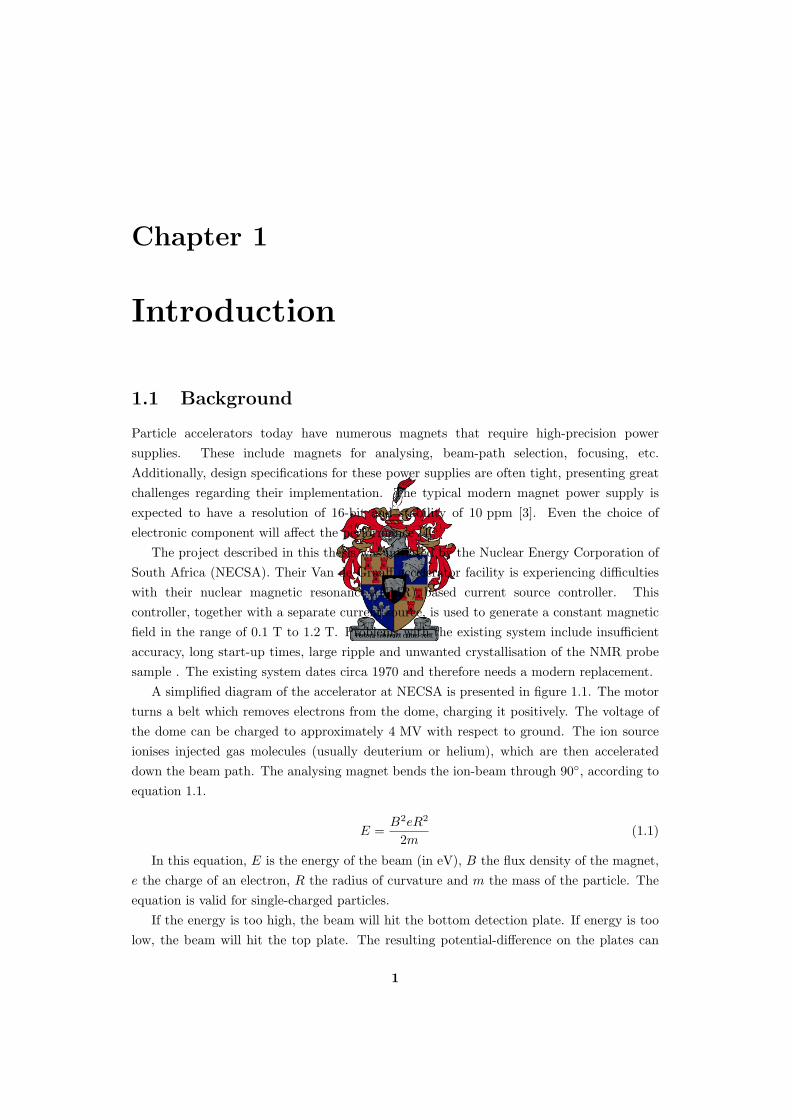
A simplified diagram of the accelerator at NECSA is presented in figure 1.1. The motorturns a belt which removes electrons from the dome, charging it positively. The voltage ofthe dome can be charged to approximately 4 MV with respect to ground. The ion sourceionises injected gas molecules (usually deuterium or helium), which are then accelerateddown the beam path. The analysing magnet bends the ion-beam through 90, according toequation 1.1.
E =B2eR2
2m(1.1)
In this equation, E is the energy of the beam (in eV), B the flux density of the magnet,e the charge of an electron, R the radius of curvature and m the mass of the particle. Theequation is valid for single-charged particles.
If the energy is too high, the beam will hit the bottom detection plate. If energy is toolow, the beam will hit the top plate. The resulting potential-difference on the plates can
1
CHAPTER 1. INTRODUCTION 21.2. RESEARCH OBJECTIVES
Chapter 1 – Introduction : Background 1
Chapter 1 – Introduction
1.0 Background Particle accelerators today have numerous magnets that require high-precision power supplies.
These include magnets for analysing, beam-path selection, focusing, etc. Additionally, design
specifications for these power supplies are often tight, presenting great challenges regarding their
implementation. The typical modern magnet power supply is expected to have a resolution of 16-bit
and stability of 10ppm [9]. Even the choice of electronic component will affect the performance [13].
The project described by this thesis was initiated by the Nuclear Energy Corporation of South
Africa (NECSA). Their Van de Graaff accelerator facility is experiencing difficulties with their nuclear
magnetic resonance (NMR) based current source controller. This controller, together with a separate
current source, is used to generate a constant magnetic field in the range of 0.1T to 1.2T. Problems
with the existing system include insufficient accuracy, long start-up times, large ripple and unwanted
crystallisation of the NMR probe sample . The existing system dates circa 1970 and therefore needs a
modern replacement.
A simplified diagram of the accelerator at NECSA is presented in figure 1.1.
Ion Source
Presurised ChamberBelt
Charged Dome
Corona Discharge Needle
Beam Path
Analysing Magnet
Target
Motor
Detection Plates
Figure 1.1 – Van de Graaff accelerator
The motor turns a belt which removes electrons from the dome, charging it positively. The
voltage of the dome can be charged to approximately 4MV with respect to ground. The ion source
ionises injected gas molecules (usually deuterium or helium), which are then accelerated down the
beam path. The analysing magnet bends the ion-beam through 90°, according to equation 1.1.
Figure 1.1: Van de Graaff accelerator
thus be measured in order to determine whether the beam energy is too high or low. Acontrol system is in place to adjust the depth of the corona discharge needle, which in turnadjusts the voltage of the dome. The result is the ability to control the energy of the beam.
This project focuses on the power supply for the analysing magnet. By adjusting themagnetic field strength, a specific beam energy is obtained.
1.2 Research Objectives
The original research objective was to develop and implement an nuclear magnetic resonance(NMR) magnetometer and control system for the existing power supply and magnet atNECSA. It was thought that this is too small a project for a masters thesis. As a result,the objectives was extended to include the design of a highly accurate power supply.
This thesis aims to target various aspects of high-performance accelerator magnet powersupplies. First the validity of implementing a truly digital controller for a high-performancepower supply is investigated. The study encompasses the control system itself as wellas digitally generated pulse width modulation (PWM). Two high-resolution digital PWMgeneration techniques are investigated. The entire digital design is implemented in a singlefield-programmable gate array (FPGA).
Second, it is intended that the final product will incorporate magnetic field-strengthfeedback as opposed to using the output current. The field strength is measured by meansof NMR. The validity of this approach is examined to discover whether NMR measurementscan be done fast and accurately enough to replace traditional current feedback. A thoroughtheoretical analysis is performed.
Third, the output range of the power supply is relatively large (over a decade) andtherefore requires special attention paid to both the NMR probe and the power supplyitself. There is much room for research in this area.

CHAPTER 1. INTRODUCTION 31.3. THESIS OVERVIEW
1.3 Thesis Overview
An examination of the existing system is performed first, along with a discussion of theexisting technology available on the market and in literature. Next, an overall design isoffered, including general block diagrams, signal definitions, component choices, etc.
The subsequent chapters deal with a detailed design of a stand-alone power supply andits control system. Output current feedback control is implemented so that experimentationmay be performed in the absence of the NMR probe. Simulation results are provided.
A new NMR measurement technique is proposed which promises excellent results withrelatively simple circuitry. Practical problems, as well as recommendations for furtherresearch into this topic, are discussed. Although very few practical results are availablefor the probe, extensive simulation results are included. A discussion of NMR theory isincluded in appendix C, together with a thorough investigation into the physics of an NMRprobe.
Next, the various systems within the controller are briefly described. The discussioncovers the design and implementation of a central processing unit (CPU) and variousperipheral drivers. Finally, practical results are provided, along with a conclusion andrecommendations.

Chapter 2
Existing Technology
2.1 Introduction
The project has been developed using the existing system at NECSA as a starting point.A thorough study of this system will follow, including an electrical model of the analysingmagnet and a brief explanation as to the operation of the NMR probe and controller.
This chapter then continues with a study of relevant existing technology. Systemsavailable on the market are mentioned and available literature is perused.
2.2 Existing System
Figure 2.1 shows the block diagram of the existing system as it is implemented at NECSA.Each block is a free-standing module.
Chapter 2 – Existing Technology : Introduction 4
Chapter 2 – Existing Technology
2.0 Introduction The project has been developed using the existing system at NECSA as a starting point. A
thorough study of this system will follow, including an electrical model of the analysing magnet and a
brief explanation as to the operation of the NMR probe and controller.
This chapter then continues with a study of relevant existing technology. Systems available on
the market are mentioned and available literature is perused.
2.1 Existing System Figure 2.1 shows the block diagram of the existing system as it is implemented at NECSA. Each
block is a free-standing module.
FrequencyCounter
AController Probe
PowerSupply
Magnet
BC
D
E
F
Figure 2.1 – Existing system block diagram
The ‘frequency counter’ is an HP model 5244L high-precision frequency counter. It provides a
precision frequency reference to the controller. It also measures the actual frequency of the NMR
probe oscillator. Table 2.I provides a list and short description of the signal groups A through F.
Figure 2.1: Existing system block diagram
The ‘frequency counter’ is an HP model 5244L high-precision frequency counter. Itprovides a precision frequency reference to the controller. It also measures the actualfrequency of the NMR probe oscillator. Table 2-I provides a list and short descriptionof the signal groups A through F.
4

CHAPTER 2. EXISTING TECHNOLOGY 52.2. EXISTING SYSTEM
Table 2-I: Existing system signals
Group Signal Description
A Frequency Reference An 1 MHz reference signal is sent to the controller
B Frequency Out The radio-frequency (RF) signal from the probe isamplified and sent to the frequency counter formeasurement
C Reference Voltage A 5.6 A·V-1 reference used to set the output of the powersupply.
D Power The probe requires ±15 V
RF Level Set A signal in the range 0 V to 2 V used to set the amplitudeof the RF signal
Modulation Signal A 50 Hz, ±110 mA sinusoidal signal that passes throughthe modulation coil in order to generate a small field-strength deviation in the vicinity of the NMR probe
Frequency Set A signal in the range 3 V to 15 V used to set the frequencyof the VCO in the probe. The actual frequency dependson the probe used.
E NMR Pulses Pulses of approximately 136 mV in amplitude which occurat the point of resonance
RF Level A voltage representing the peak-to-peak amplitude of theRF signal
RF Signal The actual RF signal
F Magnet Current The actual current through the magnet coils
2.2.1 Analysing Magnet
Figure 2.2 shows a photo of the analysing magnet at NECSA. For this project an electricalmodel of the magnet is required. Its characteristics, as revealed by the datasheet, are listedin table 2-II.
Figure 2.2: Analysing magnet at NECSA
Unfortunately, the inductance of the magnet is not given. Also, no accurate measurementof inductance could be performed on site. The inductance can, however, be mathematically

CHAPTER 2. EXISTING TECHNOLOGY 62.2. EXISTING SYSTEM
Table 2-II: Analysing magnet characteristics
Property Value In SI units
Core Solid iron
Air-gap 0.812 inches 20.6 mm
Number of turns (two coils) 1 250 1 250
Coil resistance 14.4 Ω 14.4 Ω
Rated current 15 A 15 A
Rated flux density 12 000 gauss 1.2 T
Radius of curvature 18 inches 457 mm
Field homogeneity (0.9 T) 1 part in 500 over beam path 2000 ppm
Height 94 inches 2 388 mm
Width 34.75 inches 883 mm
Length 72 inches 1 829 mm
Weight 5 000 pounds 2 268 kg
Beam-to-floor height 42 inches 1 067 mm
estimated. The formula for inductance (adapted from [5; 6] and derived in section B.2 onpage 167) is given by equations 2.1 and 2.2.
L = n2
(Aairµair
lair//
Acoreµcore
lcore
)(2.1)
B =ni
Aair
(Aairµair
lair//
Acoreµcore
lcore
)(2.2)
Where:
x//y =x · yx + y
(2.3)
Approximate dimensions of the core cross-section at the air-gap are given in figure 2.3.
Chapter 2 – Existing Technology : Existing System 6
Table 2-II – Analysing magnet characteristics
Property Value In SI units
Core Solid iron
Air-gap 0.812 inches 20.6mm
Number of turns (two coils) 1 250 1 250
Coil resistance 14.4Ω 14.4Ω
Rated current 15A 15A
Rated flux density 12 000 gauss 1.2T
Radius of curvature 18 inches 457mm
Field homogeneity (0.9T) 1 part in 500 over beam path 2000ppm
Height 94 inches 2 388mm
Width 34.75 inches 883mm
Length 72 inches 1 829mm
Weight 5 000 pounds 2 268kg
Beam-to-floor height 42 inches 1 067mm
Unfortunately, the inductance of the magnet is not given. Also, no accurate measurement could
be performed on site. The inductance can, however, be mathematically estimated. The formula for
inductance (adapted from [10] and [17]) is given by equations 2.1 and 2.2.
=
core
corecore
air
airair
lA
lAnL µµ //2 (2.1)
=
core
corecore
air
airair
air lA
lA
AniB µµ // (2.2)
Where: yxyxyx
+⋅
=// (2.3)
Approximate dimensions of the core cross-section at the air-gap are given in figure 2.3.
186mm
457mm
Figure 2.3 – Existing magnet dimensions Figure 2.3: Existing magnet dimensions
The area can then be calculated using equation 2.4 where r is the radius of curvatureand w the core width.

CHAPTER 2. EXISTING TECHNOLOGY 72.2. EXISTING SYSTEM
A =π
4
[(r +
w
2
)2
−(r − w
2
)2]
(2.4)
The magnetic field-lines fringe at the air-gap, effectively increasing the area. Accordingto [6], the equivalent air-gap can be approximated by increasing the dimensions by half theair-gap length along all the edges. Estimates of the constants are listed in table 2-III.
Table 2-III: Estimated magnet constants
Constant Value
n 1 250
Aair 0.158 m2
µair 1·µ0
lair 20.6 mm
Acore 0.139 m2
µcore 10 000·µ0
lcore 2 m
These estimates result in an inductance of 15 H. As a test for validity, the rated currentshould result in the rated flux density. This can be calculated by equation 2.2, yielding1.13 T at 15 A. In the core the flux density is 1.29 T at 15 A. Within the beam-path theflux density is somewhere between these two extremes and therefore consistent with thedatasheet value of 1.2 T.
The effect of capacitive coupling between windings and the eddy-currents in the solid-iron core is negligible at low frequencies (<10 Hz). Also, high-frequency voltage ripple wouldmanifest itself as an increase in eddy-currents in the core, rather than as an increase in themagnetic flux ripple. The power supply load is thus modelled as a 14.4 Ω resistor in serieswith a 15 H inductor.
2.2.2 Current Source
The existing power supply is a physically large, free-standing power supply. It operates byusing a servo motor to adjust a variac so that the output current follows a given voltagereference. It has a transfer constant of 5.6 A·V-1. A much-simplified schematic is given infigure 2.4.
Its bandwidth and settling time was not measured.

CHAPTER 2. EXISTING TECHNOLOGY 82.2. EXISTING SYSTEM
Chapter 2 – Existing Technology : Existing System 8
2.1.2 Current Source The existing power supply is a physically large, free-standing power supply. It operates by using
a servo motor to adjust a variac so that the output current follows a given voltage reference. It has a
transfer constant of 5.6A·V-1. A much-simplified schematic is given in figure 2.4.
M
R
3-phase in
RefLoad
Figure 2.4 – Existing power supply schematic
Its bandwidth and settling-time was not measured.
2.1.3 Probe The existing system uses an NMR technique known as continuous wave NMR (explained in
chapter 8) to probe the field strength. This technique is not as accurate as pulsed NMR, but requires
less complex electronics. Figure 2.5 shows the block-diagram of the probe [28].
OscillatorFrequency Set
EnvelopeDetector
RF Level Set
RF Signal
RF Level
NMR Pulses
Modulation Signal
Figure 2.5 – Existing probe block diagram
The change in Q-factor of the NMR coil (at resonance) is relatively small. Due to this fact, a
marginal oscillator has been implemented. This type of oscillator is very sensitive to changes in
inductor characteristics (such as Q-factor). In this system, NMR resonance will lead to amplitude
changes in the RF signal.
This change in amplitude is still very small. Also, amplitude drift may occur due to
environmental factors (especially temperature), making DC measurement impractical. To solve these
problems, the magnetic field in the vicinity of the NMR coil is modulated by a superimposed 50Hz
sinusoidal field. This field is nominally 0.4% of the main field. The effect of this technique is to take
the coil in and out of resonance repetitively, thus producing pulses. These pulses are easily amplified
by AC-coupled amplifiers and completely compensate for any environmental factors.
Figure 2.4: Existing power supply schematic
2.2.3 Probe
The existing system uses an NMR technique known as continuous wave NMR (explained insection C.5 on page 177) to probe the field strength. This technique is not as accurate aspulsed NMR, but requires less complex electronics. Figure 2.5 shows the block diagram ofthe probe [7].
Chapter 2 – Existing Technology : Existing System 8
2.1.2 Current Source The existing power supply is a physically large, free-standing power supply. It operates by using
a servo motor to adjust a variac so that the output current follows a given voltage reference. It has a
transfer constant of 5.6A·V-1. A much-simplified schematic is given in figure 2.4.
M
R
3-phase in
RefLoad
Figure 2.4 – Existing power supply schematic
Its bandwidth and settling-time was not measured.
2.1.3 Probe The existing system uses an NMR technique known as continuous wave NMR (explained in
chapter 8) to probe the field strength. This technique is not as accurate as pulsed NMR, but requires
less complex electronics. Figure 2.5 shows the block-diagram of the probe [28].
OscillatorFrequency Set
EnvelopeDetector
RF Level Set
RF Signal
RF Level
NMR Pulses
Modulation Signal
Figure 2.5 – Existing probe block diagram
The change in Q-factor of the NMR coil (at resonance) is relatively small. Due to this fact, a
marginal oscillator has been implemented. This type of oscillator is very sensitive to changes in
inductor characteristics (such as Q-factor). In this system, NMR resonance will lead to amplitude
changes in the RF signal.
This change in amplitude is still very small. Also, amplitude drift may occur due to
environmental factors (especially temperature), making DC measurement impractical. To solve these
problems, the magnetic field in the vicinity of the NMR coil is modulated by a superimposed 50Hz
sinusoidal field. This field is nominally 0.4% of the main field. The effect of this technique is to take
the coil in and out of resonance repetitively, thus producing pulses. These pulses are easily amplified
by AC-coupled amplifiers and completely compensate for any environmental factors.
Figure 2.5: Existing probe block diagram
The change in Q-factor of the NMR coil (at resonance) is relatively small. Due to thisfact, a marginal oscillator has been implemented. This type of oscillator is very sensitive tochanges in inductor characteristics (such as Q-factor). In this system, NMR resonance willlead to amplitude changes in the RF signal.
The change in amplitude is still very small. Also, amplitude drift may occur due toenvironmental factors (especially temperature), making DC measurement impractical. Tosolve these problems, the magnetic field in the vicinity of the NMR coil is modulated by asuperimposed 50 Hz sinusoidal field. This field is nominally 0.4% of the main field. The effectof this technique is to take the coil in and out of resonance repetitively, thus producing pulses.These pulses are easily amplified by AC-coupled amplifiers and completely compensate forany environmental factors.
The addition of Fe(NO3)3 decreases the time it takes for resonance to be established orceased. The concentration of the solution is 0.01 M. This enables the sample to be taken in
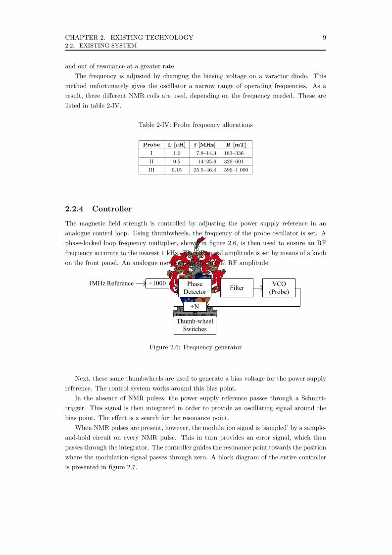
CHAPTER 2. EXISTING TECHNOLOGY 92.2. EXISTING SYSTEM
and out of resonance at a greater rate.The frequency is adjusted by changing the biasing voltage on a varactor diode. This
method unfortunately gives the oscillator a narrow range of operating frequencies. As aresult, three different NMR coils are used, depending on the frequency needed. These arelisted in table 2-IV.
Table 2-IV: Probe frequency allocations
Probe L [µH] f [MHz] B [mT]
I 1.6 7.8–14.3 183–336
II 0.5 14–25.6 329–601
III 0.15 25.5–46.4 599–1 090
2.2.4 Controller
The magnetic field strength is controlled by adjusting the power supply reference in ananalogue control loop. Using thumbwheels, the frequency of the probe oscillator is set. Aphase-locked loop frequency multiplier, shown in figure 2.6, is then used to ensure an RFfrequency accurate to the nearest 1 kHz. The RF signal amplitude is set by means of a knobon the front panel. An analogue meter shows the actual RF amplitude.
Chapter 2 – Existing Technology : Existing System 9
The addition of Fe(NO3)3 decreases the time it takes for resonance to be established or ceased.
The concentration of the solution is 0.01M. This enables the sample to be taken in and out of resonance
at a greater rate.
The frequency is adjusted by changing the biasing voltage on a varactor diode. This method
unfortunately gives the oscillator a narrow range of operating frequencies. As a result, three different
NMR coils are used, depending on the frequency needed. These are listed in table 2-IV.
Table 2-IV – Probe frequency allocations
Probe Inductance [µH] Lower f [MHz] Upper f [MHz] Lower B [mT] Upper B [mT]
I 1.6 7.8 14.3 183 336
II 0.5 14 25.6 329 601
III 0.15 25.5 46.4 599 1 090
2.1.4 Controller The magnetic field strength is controlled by adjusting the power supply reference in an analogue
control loop. Using thumbwheels, the frequency of the probe oscillator is set. A phase-locked loop
frequency multiplier, shown in figure 2.6, is then used to ensure an RF frequency accurate to the nearest
1kHz. The RF signal amplitude is set by means of a knob on the front panel. An analogue meter shows
the actual RF amplitude.
÷1000 PhaseDetector
1MHz Reference
÷N
Filter
Thumb-wheelSwitches
VCO(Probe)
Figure 2.6 – Frequency generator
Next, these same thumbwheels are used to generate a bias voltage for the power supply reference.
The control system works around this bias point.
In the absence of NMR pulses, the power supply reference passes through a Schmitt-trigger. This
signal is then integrated in order to provide an oscillating signal around the bias point. The effect is a
search for the resonance point.
When NMR pulses are present, however, the modulation signal is ‘sampled’ by a sample-and-
hold circuit on every NMR pulse. This in turn provides an error signal, which then passes through the
integrator. The controller guides the resonance point towards the position where the modulation signal
Figure 2.6: Frequency generator
Next, these same thumbwheels are used to generate a bias voltage for the power supplyreference. The control system works around this bias point.
In the absence of NMR pulses, the power supply reference passes through a Schmitt-trigger. This signal is then integrated in order to provide an oscillating signal around thebias point. The effect is a search for the resonance point.
When NMR pulses are present, however, the modulation signal is ‘sampled’ by a sample-and-hold circuit on every NMR pulse. This in turn provides an error signal, which thenpasses through the integrator. The controller guides the resonance point towards the positionwhere the modulation signal passes through zero. A block diagram of the entire controlleris presented in figure 2.7.
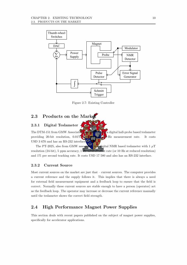
CHAPTER 2. EXISTING TECHNOLOGY 102.3. PRODUCTS ON THE MARKET
Chapter 2 – Existing Technology : Products on the Market 10
passes through zero. A block diagram of the entire controller is presented in figure 2.7.
Thumb-wheelSwitches
DAC
∑ PowerSupply Probe
Magnet
NMRDetector
Modulator
SchmittTrigger
PulseDetector
∫
Error SignalGenerator
Figure 2.7 – Existing Controller
2.2 Products on the Market 2.2.1 Digital Teslameter
The DTM-151 from GMW Associates (www.gmw.com) is a digital hall-probe based teslameter
providing 20-bit resolution, 0.01% accuracy and 10 Hz measurement rate. It costs USD3 670 and has
an RS-232 interface.
The PT-2025, also from GMW associates, is a digital NMR based teslameter with 1µT resolution
(24-bit), 5ppm accuracy, 1 Hz measurement rate (or 10 Hz at reduced resolution) and 1% per second
tracking rate. It costs USD17 580 and also has an RS-232 interface.
2.2.2 Current Source Most current sources on the market are just that – current sources. The computer provides a
current reference and the supply follows it. This implies that there is always a need for external field
measurement equipment and a feedback loop to ensure that the field is correct. Normally these current
sources are stable enough to have a person (operator) act as the feedback loop. The operator may
increase or decrease the current reference manually until the teslameter shows the correct field strength.
2.3 High Performance Magnet Power Supplies This section deals with recent papers published on the subject of magnet power supplies,
specifically for accelerator applications.
Figure 2.7: Existing Controller
2.3 Products on the Market
2.3.1 Digital Teslameter
The DTM-151 from GMW Associates (www.gmw.com) is a digital hall-probe based teslameterproviding 20-bit resolution, 0.01% accuracy and 10 Hz measurement rate. It costsUSD 3 670 and has an RS-232 interface.
The PT-2025, also from GMW associates, is a digital NMR based teslameter with 1 µTresolution (24-bit), 5 ppm accuracy, 1 Hz measurement rate (or 10 Hz at reduced resolution)and 1% per second tracking rate. It costs USD 17 580 and also has an RS-232 interface.
2.3.2 Current Source
Most current sources on the market are just that – current sources. The computer providesa current reference and the supply follows it. This implies that there is always a needfor external field measurement equipment and a feedback loop to ensure that the field iscorrect. Normally these current sources are stable enough to have a person (operator) actas the feedback loop. The operator may increase or decrease the current reference manuallyuntil the teslameter shows the correct field strength.
2.4 High Performance Magnet Power Supplies
This section deals with recent papers published on the subject of magnet power supplies,specifically for accelerator applications.

CHAPTER 2. EXISTING TECHNOLOGY 112.4. HIGH PERFORMANCE MAGNET POWER SUPPLIES
2.4.1 Topologies
High-current power supplies can often not be implemented using fast-switching converters.They resort to using phase-controlled rectifiers [8], which produce large low-frequencyharmonics. The solution is to use a switch-mode ripple regulator (SMRR) [8–10]. An SMRRis a fast-switching MOSFET or IGBT-based converter (normally in full-bridge configuration)that is either in series or in parallel with the load. These topologies are presented in figures2.8 and 2.9.
Chapter 2 – Existing Technology : High Performance Magnet Power Supplies 11
2.3.1 Topologies High-current power supplies can often not be implemented using fast-switching converters. They
resort to using phase-controlled rectifiers [14], which produce large low-frequency harmonics. The
solution is to use a switch-mode ripple regulator (SMRR) [14], [15], [25]. An SMRR is a fast-
switching MOSFET of IGBT-based converter (normally in full-bridge configuration) that is either in
series or in parallel with the load. These topologies are presented in figures 2.8 and 2.9.
SMRRMains
Load
Figure 2.8 – Series SMRR
SMRRMains
Load
Figure 2.9 – Parallel SMRR
The advantage of this topology is immediately evident. A medium-power, fast-reacting converter
supports a high-power, slow-reacting converter – both of which are easy to design and build. The
result: a high-power, fast-reacting converter, two qualities very difficult to combine otherwise.
Since the load is inductive, it is sensitive to current ripple and non-sensitive to voltage ripple.
The series SMRR minimises voltage ripple while the parallel SMRR minimises current ripple. Series
SMRR is thus more popular.
Figure 2.8: Series SMRR
Chapter 2 – Existing Technology : High Performance Magnet Power Supplies 11
2.3.1 Topologies High-current power supplies can often not be implemented using fast-switching converters. They
resort to using phase-controlled rectifiers [14], which produce large low-frequency harmonics. The
solution is to use a switch-mode ripple regulator (SMRR) [14], [15], [25]. An SMRR is a fast-
switching MOSFET of IGBT-based converter (normally in full-bridge configuration) that is either in
series or in parallel with the load. These topologies are presented in figures 2.8 and 2.9.
SMRRMains
Load
Figure 2.8 – Series SMRR
SMRRMains
Load
Figure 2.9 – Parallel SMRR
The advantage of this topology is immediately evident. A medium-power, fast-reacting converter
supports a high-power, slow-reacting converter – both of which are easy to design and build. The
result: a high-power, fast-reacting converter, two qualities very difficult to combine otherwise.
Since the load is inductive, it is sensitive to current ripple and non-sensitive to voltage ripple.
The series SMRR minimises voltage ripple while the parallel SMRR minimises current ripple. Series
SMRR is thus more popular.
Figure 2.9: Parallel SMRR
The advantage of this topology is immediately evident. A phase-controlled rectifier is ahigh-power, slow-reacting converter. The SMRR is a medium-power, fast-reacting converter.The combination of these two in the above topology yields a high-power, fast-reactingconverter – two qualities very difficult to combine otherwise.
Since the load is inductive, it is sensitive to current ripple and non-sensitive to voltageripple. The series SMRR minimises voltage ripple while the parallel SMRR minimisescurrent ripple. Series SMRR is thus more popular.
A useful method used in medium-power supplies is to follow a phase-controlled rectifierwith a buck converter [10]. The phase-controlled rectifier can then be used to soft-charge thebus capacitors at start-up, after which the buck converter takes over. This buck converteris then followed by a full-bridge. The topology is depicted in figure 2.10.
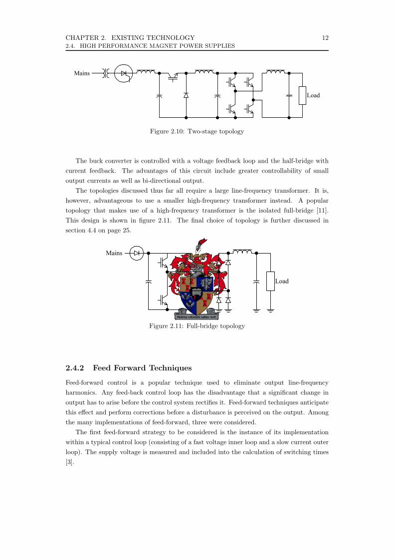
CHAPTER 2. EXISTING TECHNOLOGY 122.4. HIGH PERFORMANCE MAGNET POWER SUPPLIES
Chapter 2 – Existing Technology : High Performance Magnet Power Supplies 12
A useful method used in medium-power supplies is to follow a phase-controlled rectifier with a
buck converter [25]. The phase-controlled rectifier can then be used to soft-charge the bus capacitors at
start-up, after which the buck converter takes over. This buck converter is then followed by a full-
bridge. The topology is depicted in figure 2.10.
Mains
Load
Figure 2.10 – Two-stage topology
The buck converter is controlled with a voltage feedback loop and the half-bridge with current
feedback. The advantages of this circuit include greater controllability of small output currents as well
as bi-directional output.
The topologies discussed thus far all require a large line-frequency transformer. It is, however,
advantageous to use a smaller high-frequency transformer instead. A popular topology that makes use
of a high-frequency transformer is the isolated full-bridge [1]. This design is shown in figure 2.11.
Mains
Load
Figure 2.11 – Full-bridge topology
The final choice of topology is further discussed in chapter 4.
2.3.2 Feed Forward Techniques Feed-forward control is a popular technique used to eliminate output line-frequency harmonics.
Any feed-back control loop has the disadvantage that a significant change in output has to arise before
the control-system rectifies it. Feed-forward techniques anticipate the effect and perform corrections
before a disturbance is perceived on the output. Among the many implementations of feed-forward,
three were considered.
The first feed-forward strategy to be considered is the instance of its implementation within a
typical control loop (consisting of a fast voltage inner loop and a slow current outer loop). The supply
voltage is measured and included into the calculation of switching-times [9].
Figure 2.10: Two-stage topology
The buck converter is controlled with a voltage feedback loop and the half-bridge withcurrent feedback. The advantages of this circuit include greater controllability of smalloutput currents as well as bi-directional output.
The topologies discussed thus far all require a large line-frequency transformer. It is,however, advantageous to use a smaller high-frequency transformer instead. A populartopology that makes use of a high-frequency transformer is the isolated full-bridge [11].This design is shown in figure 2.11. The final choice of topology is further discussed insection 4.4 on page 25.
Chapter 2 – Existing Technology : High Performance Magnet Power Supplies 12
A useful method used in medium-power supplies is to follow a phase-controlled rectifier with a
buck converter [25]. The phase-controlled rectifier can then be used to soft-charge the bus capacitors at
start-up, after which the buck converter takes over. This buck converter is then followed by a full-
bridge. The topology is depicted in figure 2.10.
Mains
Load
Figure 2.10 – Two-stage topology
The buck converter is controlled with a voltage feedback loop and the half-bridge with current
feedback. The advantages of this circuit include greater controllability of small output currents as well
as bi-directional output.
The topologies discussed thus far all require a large line-frequency transformer. It is, however,
advantageous to use a smaller high-frequency transformer instead. A popular topology that makes use
of a high-frequency transformer is the isolated full-bridge [1]. This design is shown in figure 2.11.
Mains
Load
Figure 2.11 – Full-bridge topology
The final choice of topology is further discussed in chapter 4.
2.3.2 Feed Forward Techniques Feed-forward control is a popular technique used to eliminate output line-frequency harmonics.
Any feed-back control loop has the disadvantage that a significant change in output has to arise before
the control-system rectifies it. Feed-forward techniques anticipate the effect and perform corrections
before a disturbance is perceived on the output. Among the many implementations of feed-forward,
three were considered.
The first feed-forward strategy to be considered is the instance of its implementation within a
typical control loop (consisting of a fast voltage inner loop and a slow current outer loop). The supply
voltage is measured and included into the calculation of switching-times [9].
Figure 2.11: Full-bridge topology
2.4.2 Feed Forward Techniques
Feed-forward control is a popular technique used to eliminate output line-frequencyharmonics. Any feed-back control loop has the disadvantage that a significant change inoutput has to arise before the control system rectifies it. Feed-forward techniques anticipatethis effect and perform corrections before a disturbance is perceived on the output. Amongthe many implementations of feed-forward, three were considered.
The first feed-forward strategy to be considered is the instance of its implementationwithin a typical control loop (consisting of a fast voltage inner loop and a slow current outerloop). The supply voltage is measured and included into the calculation of switching times[3].

CHAPTER 2. EXISTING TECHNOLOGY 132.5. FIELD MEASUREMENT TECHNIQUES
The second feed-forward scheme is to make the saw-tooth (the signal used to generatePWM) amplitude proportional to the bus voltage. This ensures a higher duty-cycle for lowerbus-voltages and vice versa [12].
The third method uses an SMRR [9] (figure 2.8). The line voltage and output of thephase-controlled rectifier are both considered in the calculation of the SMRR duty-cycle.The output of the line-frequency filter is predicted and then compensated for. The fastdynamic response of an SMRR makes this an attractive option for large power supplies.
2.4.3 Digital Control
Digital control has numerous advantages – superior noise immunity, predictability, highaccuracy and ease of modification, to name a few. A digital interface means that manypower supplies can be connected to a single digital network. Also, measurement noise canbe filtered out. One great disadvantage, however, is digitisation error. It is for this reasonthat the PWM is usually generated with analogue circuitry [11].
Analogue PWM is generated by comparing a reference signal to a saw-tooth. This saw-tooth is often noisy and results in PWM jitter. With new technology (explained further inchapter 5) it is possible to digitally create PWM with high enough resolution (>18-bit) fordigitisation errors to become negligible. The two techniques considered in this thesis are thedelay-line and the noise-shaper [13].
Many digital control schemes exist, of which the most powerful is full state feedback[3; 14]. Full state feedback may be implemented with analogue circuitry, but this is verycomplicated. It is much simpler to use a digital implementation. An estimator [3] may beused in order to obtain the value of states that are not directly measurable.
2.5 Field Measurement Techniques
2.5.1 Calibrated Current Measurement
The measurement most often used in controlling magnet power supplies is the output current.This current may be measured using a current-sensing resistor or with a so called direct-current current-transformer (DCCT). A DCCT is a hall-probe based current transducer,such as a LEM module.
Calculating the magnetic field strength using this current measurement is always slightlyinaccurate and therefore needs calibration. The true magnetic field is measured using anNMR technique and the current measurement is then adjusted to match the actual field-strength. This calibration has to be performed quite often, as current measurement driftswith time, temperature and other environmental factors. The measurement itself is alsonoisy. Advantages of this method include high-bandwidth measurements (>10 kHz) andlow cost.

CHAPTER 2. EXISTING TECHNOLOGY 142.5. FIELD MEASUREMENT TECHNIQUES
2.5.2 Calibrated Hall Effect Probe
A better alternative to current measurement is using a hall-effect probe [15], which measuresthe field-strength directly. For larger flux densities (>300 mT), however, the hall-probemeasurement is non-linear. It drifts with temperature (600 ppm per C) and is prone tobeing noisy. Regular calibration is once again required [16]. As with calibrated currentmeasurement, this method provides high bandwidth.
2.5.3 Continuous Wave NMR
Frequency measurement and creation by means of a crystal oscillator is highly immune tonoise and environmental factors. Since NMR flux density measurement techniques are basedupon the frequency of resonance, it provides a highly accurate measurement. Continuouswave NMR [17] works on the principle that a coil undergoing resonance experiences a changein impedance. The energy absorbed by the NMR sample (usually water) manifests itself asa series resistance added to the inductance of the NMR coil.
A small radio-frequency (RF) signal is applied over the NMR coil. The frequency atwhich resonance occurs is then determined, but the response is too small to distinguish itcontinuously. To solve this problem, the sample is taken in and out of resonance repeatedly.This is performed be sweeping either the local field-strength or the frequency. The field-strength is then determined by using the highly linear relationship between the resonancefrequency and flux density. The constant involved (the gyromagnetic ratio γ) has a valueof 2.675 221 280·108 s-1·T-1 for a hydrogen nucleus. An accuracy of 100 ppm and 50 Hzbandwidth is easily obtainable.
Higher bandwidth measurements are possible by adding specific impurities to the water[18]. The effect is to decrease the time-constant of relaxation (explained in chapter 8). Abandwidth of 1 kHz is obtainable using this technique.
2.5.4 Pulsed NMR
Pulsed NMR is a very popular alternative to continuous-wave NMR [16; 18–20]. PulsedNMR uses a large RF pulse to induce an oscillation. This oscillation is then detected by theNMR coil. The frequency is determined either by means of frequency-counting the detectedsignal or by calculation of the fast Fourier transform (FFT).
An initial accurate measure of field-strength must be attained in order to calculate thefrequency of the pulse. A pulse of the wrong frequency will not induce an oscillation. Thismeasurement may be found by continuous wave NMR, calibrated hall-probe or calibratedcurrent measurements. A phase-locked loop can then be used to keep track of the resonantfrequency needed for the next pulse [20; 21].
As with continuous-wave NMR, faster update times (≈1 kHz) are made possible byadding impurities to the water sample [18]. The effect of these additions unfortunatelyresult in decreased signal strength. Therefore the detection amplifier must have a smallerbandwidth in order to detect the signal.

CHAPTER 2. EXISTING TECHNOLOGY 152.6. SUMMARY
The L-C filter used within the amplifier may be tuned by means of tuning diodes [19].The result is an amplifier that has a narrow bandwidth, but an adjustable centre frequency.The centre frequency can therefore be set to coincide with the Lamour frequency (see sectionC.2.2 on page 173) of the sample.
Pulsed NMR has superior accuracy (one part in 108 are possible [18; 22]). Drift andnoise do not pose much of a problem.
2.6 Summary
Investigation into the existing system provided insight into the solution to the problem. Thesame basic principles will be used. These include using NMR as a field-strength measurementstrategy, an output range of 1 A to 15 A, a resolution better than 20 µT, etc. The load forthe power supply may be modelled as a 14.4 Ω resistor in series with a 15 H inductor.
Various topologies are available. The most popular in the power range similar to thisproject are the buck and full-bridge converters. The isolation transformer is more often aline-frequency transformer, although some examples do use a high-frequency one.
A dual-stage topology is also popular. An example is a phase-controlled rectifier followedby full-bridge or SMRR. The advantage of dual-stage topologies is there large dynamic rangeand superior ripple rejection properties.
Digital control is prevalent, although the PWM generator is usually analogue. There aretechniques to improve the digital PWM to an acceptable resolution – for instance, using adelay-line or noise-shaper to improve digital PWM.
The field-strength can be determined in many ways. Power-supplies on the marketcommonly make use of a calibrated current measurement. This may be supported by anexternal hall-effect probe or NMR magnetometer. The existing system uses NMR to measurethe field and includes a current-controlled power supply in the control loop.
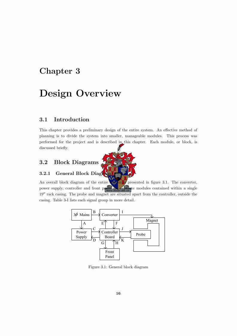
Chapter 3
Design Overview
3.1 Introduction
This chapter provides a preliminary design of the entire system. An effective method ofplanning is to divide the system into smaller, manageable modules. This process wasperformed for the project and is described in this chapter. Each module, or block, isdiscussed briefly.
3.2 Block Diagrams
3.2.1 General Block Diagram
An overall block diagram of the entire system is presented in figure 3.1. The converter,power supply, controller and front panel are separate modules contained within a single19′′ rack casing. The probe and magnet are situated apart from the controller, outside thecasing. Table 3-I lists each signal group in more detail.
Chapter 3 – Design Overview : Introduction 16
Chapter 3 – Design Overview
3.0 Introduction This chapter provides a preliminary design of the entire system. An effective method of planning
is to divide the system into smaller, manageable modules. This process was performed for the project
and described in this chapter. Each module, or block, is discussed briefly.
3.1 Block Diagrams 3.1.1 General Block Diagram
An overall block diagram of the entire system is presented in figure 3.1. The converter, power
supply, controller and front panel are separate modules contained within a single 19" rack casing. The
probe and magnet are situated apart from the controller, outside the casing. Table 3-I describes each
signal group in more detail.
Converter
ControllerBoard Probe
Magnet
PowerSupply
FrontPanel
3 Mainsφ B
AC
DG H
E F
I
J
K
Figure 3.1 – General block diagram Figure 3.1: General block diagram
16

CHAPTER 3. DESIGN OVERVIEW 173.2. BLOCK DIAGRAMS
Table 3-I: General signals
Group Signal Description
A Mains Single phase – Live and Neutral
B Mains 3-phase
C Power -12 V; -5 V; Ground; 3.3 V; 5 V; 12 V
Power Good 5 V implies that the power voltages are within acceptablerange
0 V implies that one or more power voltages are out of range
D Power Supply On 0 V switches the power supply on
5 V switches the power supply off
E Power On 5 V switches the 3-phase mains on by means of triacs,
0 V switches the 3-phase mains off
Switching Signals The output from the PWM signal generators – 4x single-endedLVPECL signals that drive the MOSFETS
F Measurements 4x analogue measurements in the range 0 V to 5 V
G LED 5x LEDs: Power; Field High; Field Low; Field Locked; Error
LCD LCD Signals: 3x Power; 2x Control; 8x Data
RS-232 To the DB-9 RS-232 port
Keypad Probe 4x Keypad probe signals (Y)
H Keypad 4x Keypad return signals (X)
Power On The power on button
Power Off The power off button
Reset The reset button
I Magnet Current The actual magnet current
J Power The probe requires 12 V
Excite An RF signal sent to the probe to drive the excitation coil –superimposed on the Power signal
K Detect An RF signal returning from the probe
3.2.2 Mains and Power Supply
A 400 V (line-line), 13 kVA, 4-wire 3-phase connection is available for use in this project.Triacs are used as a mains switch due to their small size and lack of moving parts.
One of the phases is used to power the small-signal electronics. On the primary sideof the magnet power supply, a small 2 VA, 50 Hz, 230:12 transformer is used to drive theMOSFET-driver circuitry. For the secondary side and the control board, an ATX computerpower supply is used. This has the advantage of providing various voltages (-12 V; -5 V;ground; 3.3 V; 5 V; 12 V) as well as ‘power-on’ remote control and a ‘power-good’ signal. Italso has an automatic shut-down feature when the output voltages or currents fall outsidespecifications, thus providing protection for sensitive components.
The only disadvantage is the large quiescent currents needed for the power supplyto remain regulated and ‘on’. Table 3-II shows the minimum currents required for theWIN 250PS-SPC power supply from Wintech. The resulting total minimum power is99.54 W. The total power drawn from a typical FPGA controller board is is the orderof 10 W.

CHAPTER 3. DESIGN OVERVIEW 183.2. BLOCK DIAGRAMS
Table 3-II: Power supply minimum load specification
Output voltage Minimum current
-12 V 120 mA
-5 V 120 mA
3.3 V 3 A
5 V (Standby) 400 mA
5 V 8 A
12 V 3.8 A
The total loss is therefore approximately 90 W. This is less than 3% of the converterrating and thus ignored. The minimum currents are obtained by using resistors.
3.2.3 Power Converter
A full description of the power converter design is presented in chapter 4. The need for twostages is clear. The first stage provides isolation and a variable bus-voltage for the secondstage. The topologies in mind for the first stage include the half-bridge and full-bridge.The second stage provides a means of implementing feed-forward control. Provision hasbeen made for a synchronous buck converter. This implies a total of four gate signals. Theconverter is presented in figure 3.2.
Chapter 3 – Design Overview : Block Diagrams 18
the output voltages or currents fall outside specifications, thus providing protection for sensitive
components.
The only disadvantage is the large quiescent currents needed for the power-supply to remain
regulated and ‘on’. The wasted power may be as large as 100W. This is less than 3% of the converter
rating and thus ignored.
3.1.3 Power Converter A full description of the power converter design is presented in chapter 4. At this stage in
development, the need for two stages is clear. The first stage provides a variable bus-voltage for the
second stage, as well as isolation. The topologies in mind for the first stage include the half-bridge and
full-bridge. The second stage provides a means of implementing feed-forward control. Provision has
been made for a synchronous buck converter. That implies a total of four gate signals. The converter is
presented in figure 3.2.
Stage 1Switches
Stage 1Filter Stage 2
Rectifierand
Soft-StartLoad3-Phase Mains
Gate SignalsControl Signal
Figure 3.2 – Converter block diagram
3.1.4 Probe The probe is as NMR-based probe. The controller generates an RF signal of a specific frequency
and sends it to the probe over 50Ω co-axial line. The probe then amplifies this signal and drives the
excitation coil with it. Also included in the probe is a detection circuit. It consists of a detection coil
and amplifier. The detected signal is sent back to the controller over a separate 50Ω co-axial line. A
block diagram is presented in figure 3.3.
FilterExcitation signaland Power Buffer Excitation
Coil
DetectionCoilAmplifier
Power to circuit
Detection signal
Figure 3.3 – Probe block diagram
Power is delivered to the circuit as a 12V bias voltage on the excitation signal. This reduces the
number of cables needed. BNC connectors are used.
Figure 3.2: Converter block diagram
3.2.4 Probe
The probe is an NMR-based probe. The controller generates an RF signal of a specificfrequency and sends it to the probe over 50 Ω co-axial line. The probe then amplifies thissignal and drives the excitation coil with it. Also included in the probe is a detection circuit.It consists of a detection coil and amplifier. The detected signal is sent back to the controllerover a separate 50Ω co-axial line. A block diagram is presented in figure 3.3.
Power is delivered to the circuit as a 12 V bias voltage on the excitation signal. Thisreduces the number of cables needed. BNC connectors are used.

CHAPTER 3. DESIGN OVERVIEW 193.2. BLOCK DIAGRAMS
Chapter 3 – Design Overview : Block Diagrams 18
the output voltages or currents fall outside specifications, thus providing protection for sensitive
components.
The only disadvantage is the large quiescent currents needed for the power-supply to remain
regulated and ‘on’. The wasted power may be as large as 100W. This is less than 3% of the converter
rating and thus ignored.
3.1.3 Power Converter A full description of the power converter design is presented in chapter 4. At this stage in
development, the need for two stages is clear. The first stage provides a variable bus-voltage for the
second stage, as well as isolation. The topologies in mind for the first stage include the half-bridge and
full-bridge. The second stage provides a means of implementing feed-forward control. Provision has
been made for a synchronous buck converter. That implies a total of four gate signals. The converter is
presented in figure 3.2.
Stage 1Switches
Stage 1Filter Stage 2
Rectifierand
Soft-StartLoad3-Phase Mains
Gate SignalsControl Signal
Figure 3.2 – Converter block diagram
3.1.4 Probe The probe is as NMR-based probe. The controller generates an RF signal of a specific frequency
and sends it to the probe over 50Ω co-axial line. The probe then amplifies this signal and drives the
excitation coil with it. Also included in the probe is a detection circuit. It consists of a detection coil
and amplifier. The detected signal is sent back to the controller over a separate 50Ω co-axial line. A
block diagram is presented in figure 3.3.
FilterExcitation signaland Power Buffer Excitation
Coil
DetectionCoilAmplifier
Power to circuit
Detection signal
Figure 3.3 – Probe block diagram
Power is delivered to the circuit as a 12V bias voltage on the excitation signal. This reduces the
number of cables needed. BNC connectors are used.
Figure 3.3: Probe block diagram
3.2.5 Controller
The controller consists of many components, most of which are implemented digitally. Ablock diagram is given in figure 3.4.
Chapter 3 – Design Overview : Block Diagrams 19
3.1.5 Controller The controller consists of many components, most of which are implemented digitally. A block
diagram is given in figure 3.4.
4 x ADCFrom Converter Switching SignalsControlSystem
PWMGenerator
Interface
ProbeControllerDetection Signal Excitation Signal
Figure 3.4 – Controller block diagram
The probe controller includes both an excitation pulse generator and detection circuitry. It also
includes the components required to measure the field-strength. This measured field-strength is
presented to the control system for further processing.
The control system is implemented digitally, and therefore requires analogue to digital converters.
ADCs typically have an analogue input in the range of 0 to 5V. All analogue measurements (both
voltage and current) are thus scaled to fit within that range prior to sending it to the control board.
Provision is made for four signals, although it is not clear at this stage which measurements to take.
Ribbon-cable is used for this connection with every second wire connected to ground.
The control system sends the desired duty-cycles to the PWM generator, which then generates the
switching signals.
The interface hardware is discussed in section 3.2.1. The unit may be fully computer-controlled
or free-standing. It is intended to implement a menu-driven interface.
Figure 3.4: Controller block diagram
The probe controller includes both an excitation pulse generator and detection circuitry.It also includes the components required to measure the field-strength. This measuredfield-strength is presented to the control system for further processing.
The four signals to be converted are discussed in section 5.6.3 on page 71. They arethe first filter inductor current, the load current, the first stage output voltage and the loadvoltage.
The control system is implemented digitally, and therefore requires analogue to digitalconverters. ADCs typically have an analogue input in the range of 0 to 5 V. All analoguemeasurements (both voltage and current) are thus scaled to fit within that range prior tobeing sent to the control board. Provision is made for four signals, although it is not clearat this stage which measurements to take. Ribbon-cable is used for this connection withevery second wire connected to ground.
The control system sends the desired duty-cycles to the PWM generator, which thengenerates the switching signals.
The interface hardware is discussed in section 3.3.1. The unit may be fully computer-controlled or free-standing. It is intended to implement a menu-driven interface.

CHAPTER 3. DESIGN OVERVIEW 203.3. OVERALL LAYOUT
3.3 Overall Layout
3.3.1 Front Panel
Figure 3.5 shows the design for the front panel of this project. First, there should be apower button. In this case, separate ‘on’ and ‘off’ buttons are used. There is also a ‘reset’button.
Chapter 3 – Design Overview : Overall Layout 20
3.2 Overall Layout 3.2.1 Front Panel
Figure 3.5 shows the design of the front panel of this project.
Keypad
Analysing Magnet Power Supply
LCD
Reset
Off
On
RS232
Meter 2Meter 1Field: (Low) (Locked) (High)PowerError
Figure 3.5 – Front panel layout
First, there should be a power button. In this case, separate ‘on’ and ‘off’ buttons are used. There
is also a ‘reset’ button.
Any system has indicator LEDs. There should be an indication that the power is on. A green
LED is allocated for this property. Next, there should be an indication of whether the magnet power
supply is occupied in tracking or settled on the desired value. Three LEDs are used for this task: two
red (field low and field high) and one green (field locked). The two red LEDs are ‘on’ simultaneously
when an NMR field-strength measurement is not yet available. Finally, a red error LED is included for
situations of abnormality.
A computer interface is required. A standard RS-232 serial connection has been chosen for
simplicity, which can later easily be upgraded to a USB or blue-tooth interface. A DB-9 connector is
thus included on the front-panel.
The unit should have the option of being free-standing, thus requiring a keypad (standard 4x4)
and LCD. A 4x16 LCD display was chosen. A simple menu-driven interface would be perfect for
setting the desired field-strength, re-calibrating the probe, acquiring measurements etc.
Finally, many scientists enjoy an analogue meter, since it can be read at a glance rather than
requiring interpretation of numbers. Two of these meters are included on the design of the front panel.
They are driven by a dual DAC and may be configured to show any combination of measurements.
Figure 3.5: Front panel layout
Any system has indicator LEDs. There should be an indication that the power is on. Agreen LED is allocated for this property. Next, there should be an indication of whether themagnet power supply is occupied in tracking or settled on the desired value. Three LEDsare used for this task: two red (field low and field high) and one green (field locked). Thetwo red LEDs are ‘on’ simultaneously when an NMR field-strength measurement is not yetavailable. Finally, a red LED is included for situations of abnormality.
A computer interface is required. A standard RS-232 serial connection has been chosenfor simplicity, which can later easily be upgraded to a USB or Bluetooth interface. A DB-9connector is thus included on the front-panel. USB is not included at this stage of the designbecause a USB development is not part of the research objectives.
The unit should have the option of being free-standing, thus requiring a keypad(standard 4x4) and LCD. A 4x16 LCD display was chosen. A simple menu-driven interfacewould be perfect for setting the desired field-strength, re-calibrating the probe, acquiringmeasurements and other functions.
Finally, many scientists enjoy an analogue meter, since it can be read at a glance ratherthan requiring interpretation of numbers. This idea was suggested by scientists at iThembaLabs. Two of these meters are included on the design of the front panel. They are drivenby a dual DAC and may be configured to show any combination of measurements.
3.3.2 Layout
A 19′′ rack module is convenient for installation in the NECSA accelerator facility. The insidelayout of the casing designed for this project is shown in figure 3.6. The aluminium heat sink

CHAPTER 3. DESIGN OVERVIEW 213.4. SUMMARY
also acts as an EMI shield between the noisy converter and the sensitive controller-board.The converter is considered noisy because of the high currents being switched at relativelyhigh frequencies. The controller board is considered sensitive because of the high resolution(20 µV) ADCs.
Chapter 3 – Design Overview : Summary 21
3.2.2 Layout A 19" rack module is always convenient for installation in an accelerator facility. The inside
layout of the casing designed for this project is shown in figure 3.6. The aluminium heat-sink also acts
as an EMI shield between the noisy converter and the sensitive controller-board.
Buttons
Hea
t-Sin
k an
d Sh
ield
LCDMeter 1 / RS232 Meter 2 Keypad
Computer Power Supply
Converter
Controller
Mains Probe
Figure 3.6 – General layout
3.3 Summary This chapter successfully split the design into four major components. These are the converter,
control system, probe and controller. The chapters that follow provide detail on these parts.
A brief discussion of the interface and intended layout concluded this chapter.
Figure 3.6: General layout
3.4 Summary
This chapter successfully split the design into four major components. These are theconverter, control system, probe and controller. The chapters that follow provide detailon each of these parts.
The converter was subdivided into a rectifier, first stage, high frequency transformerand a second stage. The dual stage topology offers many advantages regarding range and

CHAPTER 3. DESIGN OVERVIEW 223.4. SUMMARY
controllability.It was decided to use an NMR-based probe. The block diagram of the probe was
presented. A brief overview of the controller board was also presented.A discussion of the physical interface and intended layout concluded this chapter.

Chapter 4
Converter
4.1 Introduction
The full design for the converter hardware is presented in this chapter. The requirementsare listed and different converter topologies are considered. The passive components arecarefully designed for optimum performance. The non-ideal properties of the converter arediscussed. Waveforms are presented and analysed. The physical layout of the converter isalso discussed.
4.2 Definitions
For purposes of this thesis, some definitions are required. For clarity, some of thesedefinitions are different to the traditional ones.
Accuracy — The deviation of the output value from the absolute reference
Duty-cycle — The ratio between pulse width and switching period
Half time — The time taken for a decaying property (such as the voltage across aninductor) to decrease by half
Pulse width — The time from rising edge to falling edge of the voltage waveform at theinput of the L-C filter
Switching frequency — The reciprocal of the switching period
Switching period — The time between rising edges of the voltage waveform at the inputof the L-C filter
23
CHAPTER 4. CONVERTER 244.3. SPECIFICATION
4.3 Specification
4.3.1 Source of Power
The converter is supplied with a 4-wire 3-phase, 400 V (line-line), 13 kVA connection to theSouth African power grid (ESKOM). The voltage waveform is seldom perfectly sinusoidal,balanced or constant. A maximum variation of 10% should be incorporated into the design.
4.3.2 Power Rating and Load
It is required to drive the magnet with a DC current I of no more than 15 A. The resistanceR of the coil is 14.4 Ω. This results in a power rating P of 3.24 kW (equation 4.1), readingcloser to 3.5 kW when losses are considered.
P =I2
R(4.1)
Although inductance of the load is 15 H, the specification requires that the ripple be lessthan 10 ppm for any inductive load larger than 1 H. The inductance value that providesthe worst-case calculation is used.
4.3.3 Isolation
It is required that one side of the magnet coil be grounded, which implies an isolated powersupply. This has many implications. First, the power rating is small enough to use a high-frequency transformer. Higher power converters would require a line-frequency transformer,physically much larger than its high-frequency counterpart.
Second, a high-frequency transformer necessitates a more meticulous design, which isdiscussed in section 4.7.
4.3.4 Range
The current output range of the converter is specified as 1 A to 15 A. This translates to avoltage output range of 0 V to 216 V for a 14.4 Ω load.
A larger output voltage is required to charge the load inductor from minimum tomaximum output current within the acceptable 5 s. The same constraint lies with theopposite situation of discharging the load inductor. According to equation 4.2 [23], thegiven load will discharge from 15 A to 1 A in 2.82 s when the output voltage v is 0 V. Anoutput voltage of zero is used in this calculation because the converter is designed to beunidirectional, which means that the output cannot be negative. This leaves 2.18 s in whichthe controller must settle to 10 ppm. For a single-order system with a bandwidth of 1 Hz,the 10 ppm settling time is less than 1.83 s (see section 5.2.2 on page 55).
t =L
Rln
(v − istartR
v − iendR
)(4.2)

CHAPTER 4. CONVERTER 254.4. TOPOLOGY
Similarly, to charge the inductor from 1 A to 15 A within 2.82s requires a voltage of230.4 V. Providing for losses and other non-ideal properties, a range of 0 V to 250 V waschosen.
4.3.5 Stability
According to the specification in appendix A.3 on page 165, the system must have a stabilityof 10 ppm.
4.3.6 Audible Noise
The finished product will be installed close to the accelerator operator. It is thus requiredthat the switching noise be outside the human audible range of 20 Hz to 20 kHz [24].
4.4 Topology
4.4.1 Overall
In section 3.2.3 on page 18, the overall topology was derived to have a rectifier, two stagesand a transformer. The block diagram is repeated in figure 4.1.
Chapter 3 – Design Overview : Block Diagrams 18
the output voltages or currents fall outside specifications, thus providing protection for sensitive
components.
The only disadvantage is the large quiescent currents needed for the power-supply to remain
regulated and ‘on’. The wasted power may be as large as 100W. This is less than 3% of the converter
rating and thus ignored.
3.1.3 Power Converter A full description of the power converter design is presented in chapter 4. At this stage in
development, the need for two stages is clear. The first stage provides a variable bus-voltage for the
second stage, as well as isolation. The topologies in mind for the first stage include the half-bridge and
full-bridge. The second stage provides a means of implementing feed-forward control. Provision has
been made for a synchronous buck converter. That implies a total of four gate signals. The converter is
presented in figure 3.2.
Stage 1Switches
Stage 1Filter Stage 2
Rectifierand
Soft-StartLoad3-Phase Mains
Gate SignalsControl Signal
Figure 3.2 – Converter block diagram
3.1.4 Probe The probe is as NMR-based probe. The controller generates an RF signal of a specific frequency
and sends it to the probe over 50Ω co-axial line. The probe then amplifies this signal and drives the
excitation coil with it. Also included in the probe is a detection circuit. It consists of a detection coil
and amplifier. The detected signal is sent back to the controller over a separate 50Ω co-axial line. A
block diagram is presented in figure 3.3.
FilterExcitation signaland Power Buffer Excitation
Coil
DetectionCoilAmplifier
Power to circuit
Detection signal
Figure 3.3 – Probe block diagram
Power is delivered to the circuit as a 12V bias voltage on the excitation signal. This reduces the
number of cables needed. BNC connectors are used.
Figure 4.1: Overall topology block diagram
The reasons for a dual stage topology is more clear at this point. For a single stagesystem, the pulse height is fixed. This means that a very small duty cycle will be requiredfor a small output current. This small duty cycle is difficult to generate accurately. Byadding a second stage, the pulse hight is adjustable. This means that the duty cycle for theoutput stage may be high (80%). It is therefore more practical to generate the duty cycleaccurately.
Another problem is the non-ideal properties of the transformer. The duty-cycle of thegate signals and that of the voltage waveform at the input to the L-C filter is slightlydifferent due to the leakage inductance of the transformer (see section 4.7.3 on page 44).This difference is not constant as it depends on the inductor current at that time. It is thusdifficult to compensate for this error fully.

CHAPTER 4. CONVERTER 264.4. TOPOLOGY
The second stage has a much more predictable duty-cycle and is therefore more accuratelycontrollable. The errors caused by the effect described in the previous paragraph can beremoved by means of a feed-forward control scheme.
4.4.2 Rectifier
The DC bus is generated by rectifying the 3-phase mains. This may be achieved, in orderof complexity, by means of a matrix converter [25], an active rectifier [6], phase-controlledrectifier [8] or passive rectifier (diode-bridge) [6]. A comparison of these options is presentedin table 4-I.
Table 4-I: Rectifier comparison
Property Simplified Active Phase- Passive
matrix rectifier controlled rectifier
converter rectifier
Power flow Bidirectional Bidirectional Unidirectional Unidirectional
Output voltage 0 to 540 V 540 V to 800 V 0 to 540 V 566 V
range from (using 800 V
400 V 3-phase MOSFETs)
External No Yes No Yes
converter?
Synchronised Yes Yes Yes No
to mains?
Switches 12x MOSFET / 6x MOSFET / 6x Thyristor 6x Diode
IGBT IGBT
Filter inductor 3-phase HF 3-phase HF Single LF None
External No Yes No Yes
soft-start?
Supply current Sinusoidal Sinusoidal Square Pulsed
waveform
If budget and development times were of no consideration, a matrix converter wouldhave been the option of choice. A matrix converter requires complex support circuitry,especially in an isolated converter. Apart from the 12 gate-signals, the gate driversthemselves are complex. It also requires the measurement of supply voltages and currents.These measurements are on the primary side and therefore need an isolated communicationstandard to bring them to the secondary side for processing.
The same problems exist for an active rectifier, with an added disadvantage being thatit requires a separate converter to adjust the bus-voltage. The reason for this is the factthat the resulting bus voltage is higher than the peak line-to-line voltage.
This leaves only the phase-controlled rectifier and passive rectifier, which can becontrolled with a relatively simple analogue circuit. The large low-frequency filter inductor
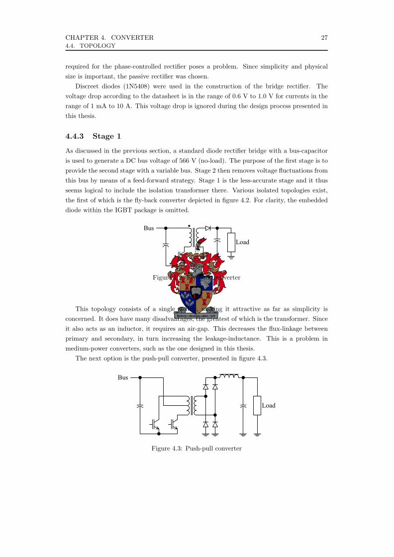
CHAPTER 4. CONVERTER 274.4. TOPOLOGY
required for the phase-controlled rectifier poses a problem. Since simplicity and physicalsize is important, the passive rectifier was chosen.
Discreet diodes (1N5408) were used in the construction of the bridge rectifier. Thevoltage drop according to the datasheet is in the range of 0.6 V to 1.0 V for currents in therange of 1 mA to 10 A. This voltage drop is ignored during the design process presented inthis thesis.
4.4.3 Stage 1
As discussed in the previous section, a standard diode rectifier bridge with a bus-capacitoris used to generate a DC bus voltage of 566 V (no-load). The purpose of the first stage is toprovide the second stage with a variable bus. Stage 2 then removes voltage fluctuations fromthis bus by means of a feed-forward strategy. Stage 1 is the less-accurate stage and it thusseems logical to include the isolation transformer there. Various isolated topologies exist,the first of which is the fly-back converter depicted in figure 4.2. For clarity, the embeddeddiode within the IGBT package is omitted.
Chapter 4 – Converter : Topology 26
If budget and development times were of no consideration, a matrix converter would have been
the perfect option. A matrix converter does, however, require complex support circuitry, especially in
an isolated converter. Apart from the 18 gate-signals – the gate drivers themselves are complex – it
requires the measurement of supply voltage and current. These measurements are both on the primary
side and therefore need some isolated communication standard to bring them to the secondary side for
processing.
The same problems exist for an active rectifier, with an added disadvantage being that it requires
a separate converter to adjust the bus-voltage. The reason for this is the fact that the resulting bus
voltage is higher than the peak line-to-line voltage of mains.
This leaves only the phase-controlled rectifier and passive rectifier, which can be controlled with
a relatively simple analogue circuit. The large low-frequency filter inductor required for the phase-
controlled rectifier poses a problem. Since simplicity and physical size is important, the passive
rectifier has been chosen. This is a low-power converter, therefore the harmonic content of the supply
current is easily reduced to accepted limits by means of a standard EMI filter.
4.2.2 Stage 1 As discussed in the previous section, a standard diode rectifier bridge with a bus-capacitor is used
to generate a DC bus voltage of 535V (average at full-load). The purpose of the first stage is to provide
the second stage with a variable bus. Stage 2 then cleans this bus-voltage by means of a feed-forward
strategy. Stage 1 is the less-accurate stage and it thus seems logical to include the isolation transformer
here. Various isolated topologies exist, the first of which is the fly-back converter depicted in figure
4.1.
Bus
Load
Figure 4.1 – Fly-back converter
This topology consists of a single switch, making it attractive as far as simplicity is concerned. It
does unfortunately have many disadvantages, the greatest of which is the transformer. Since it also
acts as an inductor, it requires an air-gap. This decreases the flux-linkage between primary and
secondary, in turn increasing the spray-inductance. This is a problem in medium-power converters,
such as the one designed in this thesis.
Figure 4.2: Fly-back converter
This topology consists of a single switch, making it attractive as far as simplicity isconcerned. It does have many disadvantages, the greatest of which is the transformer. Sinceit also acts as an inductor, it requires an air-gap. This decreases the flux-linkage betweenprimary and secondary, in turn increasing the leakage-inductance. This is a problem inmedium-power converters, such as the one designed in this thesis.
The next option is the push-pull converter, presented in figure 4.3.
Chapter 4 – Converter : Topology 27
The next option is the push-pull converter, presented in figure 4.2.
Bus
Load
Figure 4.2 – Push-pull converter
Both of the switches are driven with respect to ground, thereby making it an attractive option. It
also uses the entire B-H curve of the transformer core, thus allowing a smaller transformer to be used.
The catch comes in the bus-voltage. When the one switch is on, the other has to withstand double the
bus-voltage (1120V in this case). This is not possible for practical MOSFETs. Also, the topology has
problems with core saturation and requires extra circuitry to prevent a DC current from flowing.
The two topologies to be considered in more depth are thus the half-bridge and full-bridge.
Simplified schematics are shown in figures 4.3 and 4.4 and a comparison is given in table 4-II.
Bus
Load
Figure 4.3 – Isolated half-bridge converter
Bus
Load
Figure 4.4 – Isolated full-bridge converter
Figure 4.3: Push-pull converter

CHAPTER 4. CONVERTER 284.4. TOPOLOGY
Both of the switches are driven with respect to ground, thereby making it an attractiveoption. It also uses the entire B-H curve of the transformer core, thus allowing a smallertransformer to be used.
The high bus-voltage poses a problem. When the one switch is on, the other has towithstand double the bus-voltage (1 132 V in this case). This is not possible for practicalMOSFETs. Also, the topology has problems with core saturation and requires extra circuitryto prevent a DC current from flowing.
The two topologies to be considered in more depth are thus the half-bridge and full-bridge. Simplified schematics are shown in figures 4.4 and 4.5 and a comparison is given intable 4-II.
Chapter 4 – Converter : Topology 27
The next option is the push-pull converter, presented in figure 4.2.
Bus
Load
Figure 4.2 – Push-pull converter
Both of the switches are driven with respect to ground, thereby making it an attractive option. It
also uses the entire B-H curve of the transformer core, thus allowing a smaller transformer to be used.
The catch comes in the bus-voltage. When the one switch is on, the other has to withstand double the
bus-voltage (1120V in this case). This is not possible for practical MOSFETs. Also, the topology has
problems with core saturation and requires extra circuitry to prevent a DC current from flowing.
The two topologies to be considered in more depth are thus the half-bridge and full-bridge.
Simplified schematics are shown in figures 4.3 and 4.4 and a comparison is given in table 4-II.
Bus
Load
Figure 4.3 – Isolated half-bridge converter
Bus
Load
Figure 4.4 – Isolated full-bridge converter
Figure 4.4: Isolated half-bridge converter
Chapter 4 – Converter : Topology 27
The next option is the push-pull converter, presented in figure 4.2.
Bus
Load
Figure 4.2 – Push-pull converter
Both of the switches are driven with respect to ground, thereby making it an attractive option. It
also uses the entire B-H curve of the transformer core, thus allowing a smaller transformer to be used.
The catch comes in the bus-voltage. When the one switch is on, the other has to withstand double the
bus-voltage (1120V in this case). This is not possible for practical MOSFETs. Also, the topology has
problems with core saturation and requires extra circuitry to prevent a DC current from flowing.
The two topologies to be considered in more depth are thus the half-bridge and full-bridge.
Simplified schematics are shown in figures 4.3 and 4.4 and a comparison is given in table 4-II.
Bus
Load
Figure 4.3 – Isolated half-bridge converter
Bus
Load
Figure 4.4 – Isolated full-bridge converter Figure 4.5: Isolated full-bridge converter
Table 4-II: Half-bridge vs full-bridge
Property Half-bridge Full-bridge
Number of switches 2 4
Capacitor Bus capacitor with centre-tap Low-voltage bipolar
Leakage-inductance problem Oscillations Inaccurate duty-cycle
Switched current Twice that of full-bridge Half that of half-bridge
Transformer primary voltages 283 V 566 V
CHAPTER 4. CONVERTER 294.4. TOPOLOGY
The full-bridge has many advantages over the half-bridge and was chosen. The greatestadvantages of the full-bridge are the ability to enforce a zero state as well as the fact thatit switches half the current (compared to the half-bridge). This means fewer problems withleakage inductance and EMI.
The transformer must have double the turns, implying up to four times the leakageinductance for the same configuration. This does not pose a problem, as the voltage isdoubled and the current halved, which cancels out the effect of the higher inductance – thedischarge time is the same.
Since the switching times of the two switches are never exactly the same, it is possiblefor a DC voltage component to exist across the transformer. The effect is that a DC currentgrows in the primary of the transformer, which eventually saturates the core. A capacitorin series with the transformer solves this problem. It is easy to show that the peak-to-peakvoltage ripple across this capacitor is given by equation 4.3, where D is the duty-cycle, f
the switching frequency, C the capacitance and i the current through the capacitor whilethe switches are cross-conducting.
∆v =Di
Cf(4.3)
For a capacitance of 100 µF, maximum current of 12 A and a switching frequency of47.684 kHz, the voltage ripple is 2.5 V. This is for a duty-cycle of unity, which is the worstcase scenario. It is assumed that the maximum DC voltage is given by the uncertainty ofswitching times, i.e. ±250 ps due to the gate-resistances and 200 ns due to the MOSFETdriver. The 200 ns translates to a duty-cycle uncertainty of 1%, which implies a DC offsetof 5.66 V for a 566 V bus. A 16 V capacitor would thus be sufficient. Ten 16 V, 10 µFceramic capacitors (1206 package) were connected in parallel to form the required 100 µFseries capacitor. The transient voltage fluctuations are kept at a minimum by means of asoft start mechanism and low closed-loop bandwidth.
4.4.4 Stage 2
There are various topologies available that offer a directly proportional relationship betweencycle-average voltage and duty-cycle. This proportional relationship is very convenient forthe implementation of feed-forward. Two topologies which satisfy this requirement are thebuck-converter and the full-bridge. Since a unidirectional output current (and voltage) isrequired, the buck-converter topology was chosen.
One detail to be considered is the presence or absence of a bottom switch. In otherwords: is a normal buck converter or a synchronous buck (half-bridge) converter used?The bottom switch offers numerous advantages. These include a guarantee of continuousinductor current, bi-directional power flow and lower conduction-losses.
The bottom switch may be replaced, however, by a diode. Silicon-carbide diodes havethe advantage of zero reverse-recovery and therefore less switching losses. It is possible thatthe filter inductor carries negative or zero current during transients. If that be the case, the
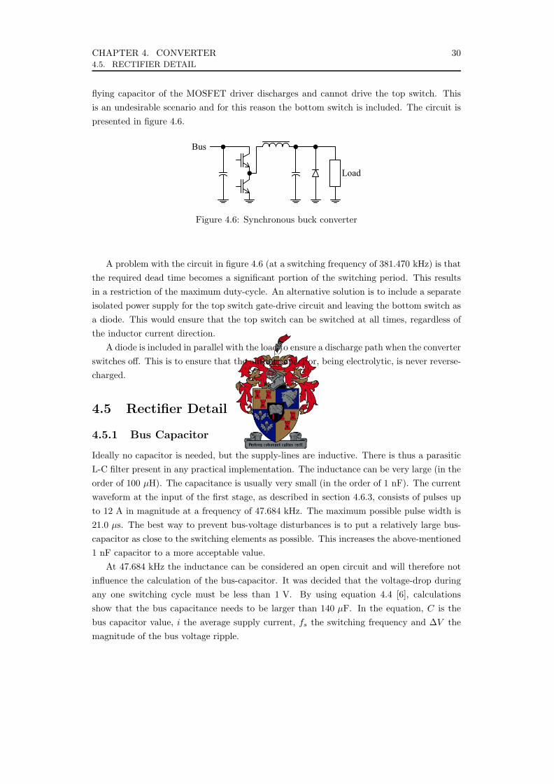
CHAPTER 4. CONVERTER 304.5. RECTIFIER DETAIL
flying capacitor of the MOSFET driver discharges and cannot drive the top switch. Thisis an undesirable scenario and for this reason the bottom switch is included. The circuit ispresented in figure 4.6.
Chapter 1 – Converter : Soft-Start 8
1.2.3 Stage 2 There are few topologies available that offer a directly proportional relationship between cycle-
average voltage and duty-cycle. This proportional relationship is very convenient for the
implementation of feed-forward. The two topologies which satisfy this requirement are the buck-
converter and the full-bridge. Since a unidirectional output current is required, the buck-converter has
been chosen.
One added detail to be considered is the presence or absence of a bottom switch. In other words:
is a normal buck converter or a synchronous buck (half-bridge) converter used? The bottom switch
does offer numerous advantages. These include a guarantee of continuous inductor current, bi-
directional power flow, lower conduction-losses, etc.
The bottom switch may be replaced, however, by a silicon-carbide diode. This has the advantage
of zero reverse-recovery and therefore less switching losses. Since the converter drives a large
inductor, the current would always be positive. The current-ripple is designed to be very small. For
these reasons it is assumed that the inductor will never carry discontinuous current and power always
flows towards the load. The circuit is presented in figure 4.5.
Load
Bus
Figure 1.5 – Buck converter
A diode is included in parallel with the load to ensure a discharge path when the converter rapidly
switches off and remains off. This is to ensure that the output capacitor, being electrolytic, is never
reverse-charged.
1.3 Soft-Start 1.3.1 DC-Bus
Rectified 400V 3-phase is never smaller than 490V. For this reason, and considering the
relatively large bus-capacitor, the system cannot simply be switched on without causing damage. The
capacitor must be charged slowly before it can be connected directly to the mains. This can be done in
many ways.
Figure 4.6: Synchronous buck converter
A problem with the circuit in figure 4.6 (at a switching frequency of 381.470 kHz) is thatthe required dead time becomes a significant portion of the switching period. This resultsin a restriction of the maximum duty-cycle. An alternative solution is to include a separateisolated power supply for the top switch gate-drive circuit and leaving the bottom switch asa diode. This would ensure that the top switch can be switched at all times, regardless ofthe inductor current direction.
A diode is included in parallel with the load to ensure a discharge path when the converterswitches off. This is to ensure that the output capacitor, being electrolytic, is never reverse-charged.
4.5 Rectifier Detail
4.5.1 Bus Capacitor
Ideally no capacitor is needed, but the supply-lines are inductive. There is thus a parasiticL-C filter present in any practical implementation. The inductance can be very large (in theorder of 100 µH). The capacitance is usually very small (in the order of 1 nF). The currentwaveform at the input of the first stage, as described in section 4.6.3, consists of pulses upto 12 A in magnitude at a frequency of 47.684 kHz. The maximum possible pulse width is21.0 µs. The best way to prevent bus-voltage disturbances is to put a relatively large bus-capacitor as close to the switching elements as possible. This increases the above-mentioned1 nF capacitor to a more acceptable value.
At 47.684 kHz the inductance can be considered an open circuit and will therefore notinfluence the calculation of the bus-capacitor. It was decided that the voltage-drop duringany one switching cycle must be less than 1 V. By using equation 4.4 [6], calculationsshow that the bus capacitance needs to be larger than 140 µF. In the equation, C is thebus capacitor value, i the average supply current, fs the switching frequency and ∆V themagnitude of the bus voltage ripple.

CHAPTER 4. CONVERTER 314.5. RECTIFIER DETAIL
C ≈ i
fs∆V(4.4)
The capacitor must be able to withstand a maximum of 622 V (see section 4.5.3 onpage 32). Two 400 V, 470 µF capacitors in series would thus be sufficient. Large parallelresistances (390 kΩ) are included to ensure even voltage-distribution. Since the dioderectifier does not allow current to flow back into mains, no damping is required.
4.5.2 Waveforms
Figures 4.7a and 4.8 show the P-SPICE simulated bus voltage under different conditions.The 400 V 3-phase mains was rectified using 1N5408 diodes and filtered by a 235 µFcapacitor. A current source was used to emulate the load. The current was calculatedby dividing the power by 566 V.
In figure 4.7a the capacitor is being charged through a 500 Ω resistor under no load. Fromthe resulting curve it is clear that the soft-start process requires 1.5 s before the resistor canbe shorted out. More about this in section 5.8.1 on page 82.
Figure 4.7b shows the waveform under the minimum load of 14.4 W. The average currentthat is drawn from the DC bus is 25.4 mA. The voltage drop may be approximated usingequation 4.5 [23], where fR is the rectified waveform frequency of 300 Hz. Using equation4.5, the expected voltage drop is 361 mv, which is confirmed by figure 4.7b
∆V ≈ i
CfR(4.5)
(a) Soft-start (b) Minimum load: 14.4 W
Figure 4.7: DC bus waveforms
Figure 4.8 shows the results when repeating the process for a medium load (500 W) andthe maximum load (3.5 kW). The average currents are 883 mA and 6.18 A respectively.The expected voltage drops are 12.53 V and 87.71 V respectively. These calculated valuesdiffer from the simulated waveforms because equation 4.5 does not take the crest of therectified sinusoidal wave into account, but rather assumes an immediate drop upon reaching
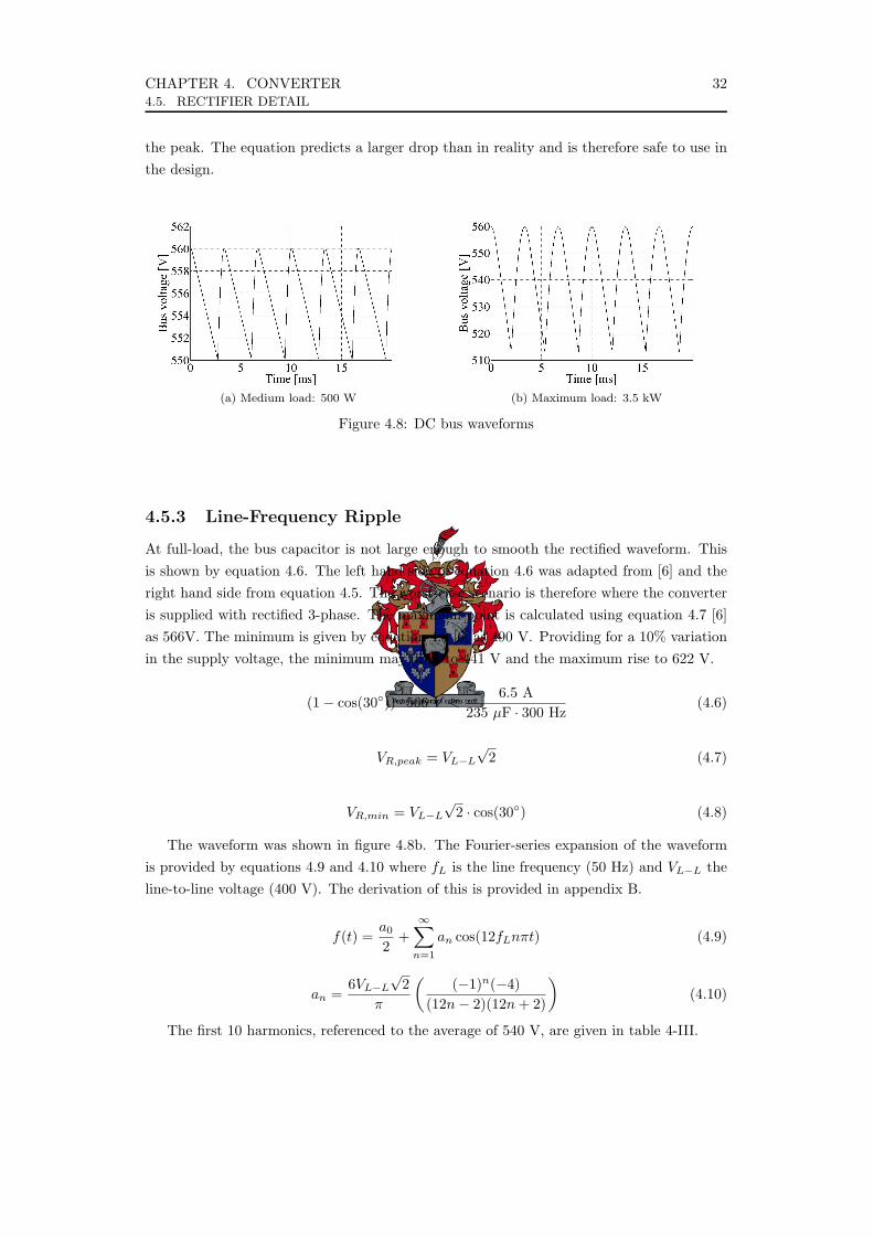
CHAPTER 4. CONVERTER 324.5. RECTIFIER DETAIL
the peak. The equation predicts a larger drop than in reality and is therefore safe to use inthe design.
(a) Medium load: 500 W (b) Maximum load: 3.5 kW
Figure 4.8: DC bus waveforms
4.5.3 Line-Frequency Ripple
At full-load, the bus capacitor is not large enough to smooth the rectified waveform. Thisis shown by equation 4.6. The left hand side of equation 4.6 was adapted from [6] and theright hand side from equation 4.5. The worst-case scenario is therefore where the converteris supplied with rectified 3-phase. The maximum point is calculated using equation 4.7 [6]as 566V. The minimum is given by equation 4.8 [6] as 490 V. Providing for a 10% variationin the supply voltage, the minimum may drop to 441 V and the maximum rise to 622 V.
(1− cos(30)) · 566 V <6.5 A
235 µF · 300 Hz(4.6)
VR,peak = VL−L
√2 (4.7)
VR,min = VL−L
√2 · cos(30) (4.8)
The waveform was shown in figure 4.8b. The Fourier-series expansion of the waveformis provided by equations 4.9 and 4.10 where fL is the line frequency (50 Hz) and VL−L theline-to-line voltage (400 V). The derivation of this is provided in appendix B.
f(t) =a0
2+
∞∑n=1
an cos(12fLnπt) (4.9)
an =6VL−L
√2
π
((−1)n(−4)
(12n− 2)(12n + 2)
)(4.10)
The first 10 harmonics, referenced to the average of 540 V, are given in table 4-III.
CHAPTER 4. CONVERTER 334.5. RECTIFIER DETAIL
Table 4-III: Bus harmonic content
Harmonic Frequency [Hz] Amplitude [dB]
1 300 -25
2 600 -37
3 900 -44
4 1200 -49
5 1500 -53
6 1800 -56
7 2100 -59
8 2400 -61
9 2700 -63
10 3000 -65
4.5.4 Ripple Current Through Bus Capacitor
According to the datasheet of the 470 µF, 400 V capacitors, the maximum rms currentripple is 8 A at 120 Hz and 80 C. The equivalent series resistance is 100 Ω at 120 Hz.According to PSpice simulation, the rms current ripple at full load (3 500 W) is 7.2 A. Thesame conditions as in section 4.5.2 were used. It can therefore be concluded that the abovearrangement is practically viable.
4.5.5 Losses
There is very little loss in the rectifier circuit. The larger power loss is through the soft-startresistor bypass MOSFET. Its RMS current is 6 A and passes through a 99 mΩ resistor. Thisimplies a loss of 3.5 W.
It can be assumed that the average current through each of the diodes in the rectifier is2 A. The voltage drop at that current across a 1N5408 (the chosen diode for constructingthe rectifier) is less than 1 V. This means a loss of 2 W through each diode. Accordingto the datasheet, the ambient temperature must be below 75 C for an average current of2.5 A per diode.
4.5.6 Supply Current
The supply current resulting from a passive rectifier is very far from sinusoidal. Figure4.9 shows the PSpice simulation of the line current at full load, together with a frequencyspectrum calculated using an FFT algorithm. The simulation uses a 1N5408 diode bridgerectifier, 235 µF bus capacitor and a 90 Ω load resistor.
A line-frequency filter, such as a standard EMI filter, must be inserted before the rectifierin order to lower the total harmonic distortion of the line current. Alternatively, futureimplementations of the power supply may use an active rectifier, which has sinusoidalcurrent. The prototype has no filter.
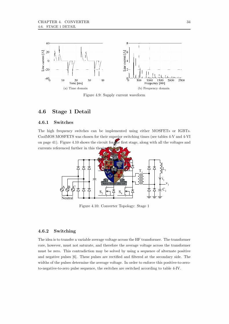
CHAPTER 4. CONVERTER 344.6. STAGE 1 DETAIL
(a) Time domain (b) Frequency domain
Figure 4.9: Supply current waveform
4.6 Stage 1 Detail
4.6.1 Switches
The high frequency switches can be implemented using either MOSFETs or IGBTs.CoolMOS MOSFETS was chosen for their superior switching times (see tables 4-V and 4-VIon page 41). Figure 4.10 shows the circuit for the first stage, along with all the voltages andcurrents referenced further in this thesis.
Chapter 4 – Converter : Summary 50
The copper thickness on the power PCB is 70µm. This means that a conductor carrying 15A
must be 8mm wide. Similarly, a 6A track must be 2mm and a 12A track 6mm. These widths have been
calculated using the “Track Amp Calculator” from North Tech Services (http://www.ntspcb.co.za). A
temperature difference of 10°C has been assumed.
4.13 Summary After considering the requirements, a two-stage topology has been chosen. The two stages are
implemented as an isolated full-bridge (figure 4.28) and a buck converter (figure 4.29) respectively.
A B C
Neutral
S1
S2
T1
S3
S4
L1
C1
i1v1
566V
Figure 4.28 – Converter Topology: Stage 1
RLoad
LLoad
L2S5
v2 i2
v1
v3i3
C2
Figure 4.29 – Converter Topology: Stage 2
The bus capacitor was designed as two 470µF, 400V capacitors in series. Both filter capacitors
are the same 400V, 470µF capacitors. The filter inductors L1 and L2 were calculated to be 3mH and
200µH respectively. Their physical construction was provided.
The transformer has been designed with a 1:1 winding ration and twisted-pair windings. The
leakage inductance was measured as 4µH and the effect has been studied. The dead-time of 500ns was
found to remove the effect of leakage inductance.
Furthermore, the soft-start sequence has been chosen. The two duty-cycles, D1 and D2, are to be
ramped to 13% and 80%, respectively, in 2s. After this the control system may take over.
The total losses of the components to be bolted to the heat-sink were calculated as 70W. A fan
would thus need to be included as part of the casing.
Figure 4.10: Converter Topology: Stage 1
4.6.2 Switching
The idea is to transfer a variable average voltage across the HF transformer. The transformercore, however, must not saturate, and therefore the average voltage across the transformermust be zero. This contradiction may be solved by using a sequence of alternate positiveand negative pulses [6]. These pulses are rectified and filtered at the secondary side. Thewidths of the pulses determine the average voltage. In order to enforce this positive-to-zero-to-negative-to-zero pulse sequence, the switches are switched according to table 4-IV.
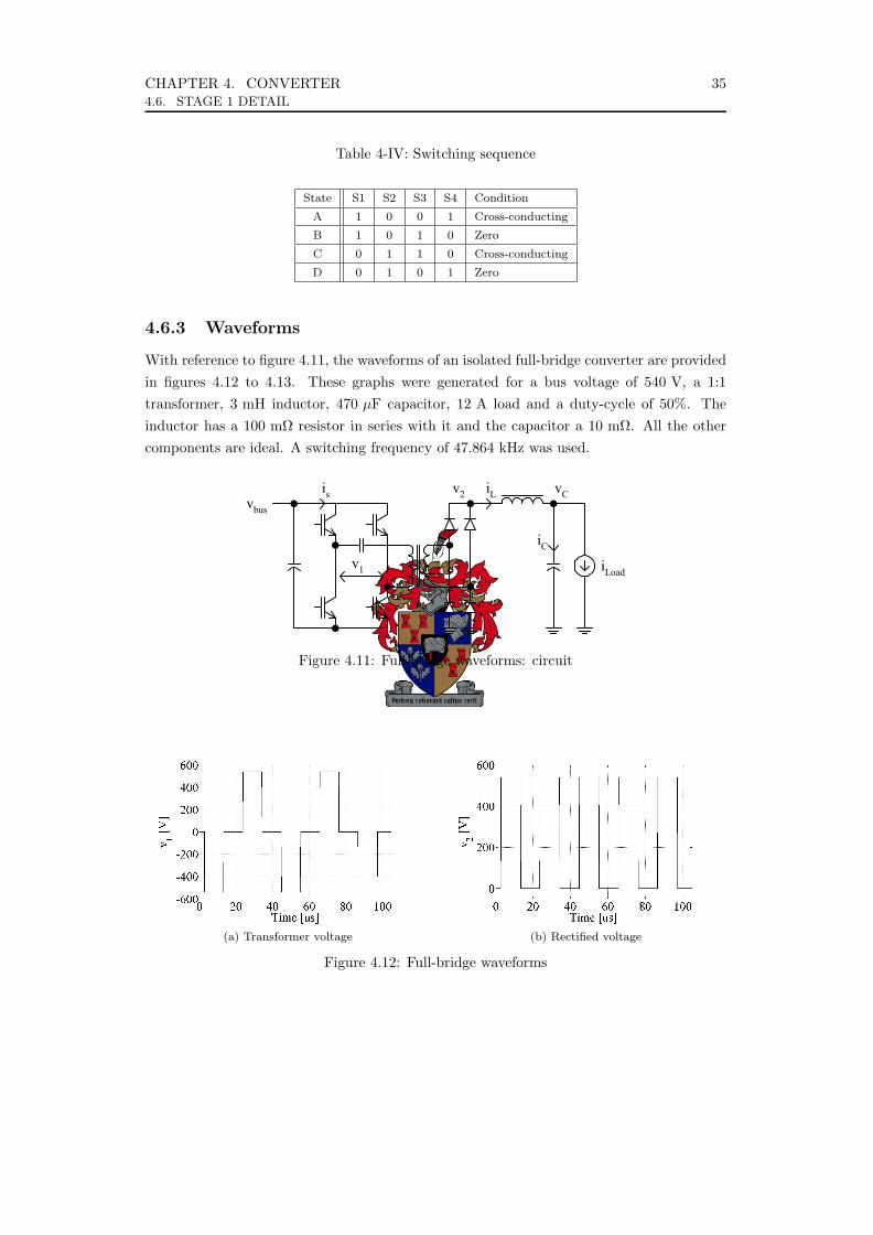
CHAPTER 4. CONVERTER 354.6. STAGE 1 DETAIL
Table 4-IV: Switching sequence
State S1 S2 S3 S4 Condition
A 1 0 0 1 Cross-conducting
B 1 0 1 0 Zero
C 0 1 1 0 Cross-conducting
D 0 1 0 1 Zero
4.6.3 Waveforms
With reference to figure 4.11, the waveforms of an isolated full-bridge converter are providedin figures 4.12 to 4.13. These graphs were generated for a bus voltage of 540 V, a 1:1transformer, 3 mH inductor, 470 µF capacitor, 12 A load and a duty-cycle of 50%. Theinductor has a 100 mΩ resistor in series with it and the capacitor a 10 mΩ. All the othercomponents are ideal. A switching frequency of 47.864 kHz was used.
Chapter 4 – Converter : Wave-Forms 34
Figure 4.11 – DC-bus wave-forms: medium load (500W)
Figure 4.12 – DC-bus wave-forms: maximum load (3.5kW)
4.6.2 Stage 1 With reference to figure 4.13, the wave-forms of an isolated full-bridge converter are provided in
figures 4.13 to 4.18.
vbus
v1
iLv2 vC
iC
iLoad
is
Figure 4.13 – Full-bridge wave-forms: circuit
Figure 4.14 – Full-bridge wave-forms: v1
Figure 4.11: Full-bridge waveforms: circuit
(a) Transformer voltage (b) Rectified voltage
Figure 4.12: Full-bridge waveforms

CHAPTER 4. CONVERTER 364.6. STAGE 1 DETAIL
(a) Capacitor current (b) Output voltage
Figure 4.13: Full-bridge waveforms
(a) Inductor current (b) Supply current
Figure 4.14: Full-bridge waveforms
Figure 4.12a shows the voltage across the transformer (v1). The first pulse is negative,which corresponds to S2 and S3 being closed. Then S3 opens. The current stored in theleakage inductance of the transformer finds a path through the diode of S4, making v1 zero.The current in now ‘stored’ in the leakage inductance because of this zero voltage drop.In a practical system the on voltage of the diode in combination with the on resistance ofthe MOSFET will generate a voltage over the transformer, but this is small enough to beignored at this point. Switch S4 therefore switches on when the voltage across it is alreadyzero, resulting in no switching loss.
The next part of the cycle is where S2 opens, letting the current find a path throughthe diode in S1. This corresponds to the second pulse. The leakage inductance now rapidlydischarges, but before it can fully discharge, S1 closes. This is also a zero voltage switchingcondition and therefore results in no switching loss. The secondary of the transformer isstill zero at this point. This is because the current is in the ‘wrong’ direction. The diodebridge on the secondary side prevents the voltage from rising until the current has turnedaround. This is a very short and has little effect.
The process continues with S4 closing, letting the current go through the diode in S3,

CHAPTER 4. CONVERTER 374.6. STAGE 1 DETAIL
zeroing the voltage again. The current is once again trapped and S3 closes while there iszero voltage across it. Finally S1 opens, S2 closes and the process repeats itself.
Besides from the little delay in rising-edge, the secondary waveform of the transformeris identical to the primary. This is then rectified, producing figure 4.12b.
It may be assumed that the output voltage vC is constant for all practical purposes, ascan be seen in figure 4.13b. During a ‘high’ pulse or a ‘low’ pulse the voltage across theinductor is also constant. This means that the current in the inductor must rise and falllinearly, as can be seen in figure 4.14a. The average current must be the same as the outputcurrent (11.95 A in this case) in order for the system to be in steady state.
Figure 4.14b shows the supply current. This is the same as the rising sections of theinductor current. By tracing the path taken by the current through the switches this caneasily be explained. While in a zero state, the current simply circulates through either thetop two or bottom two switches. While in a non-zero state, the current flows from the bus,through the transformer and back through the bus capacitor. These are the pulses observedin figure 4.14b
Since the current though the load is nearly constant, the ripple component of the inductormust flow though the capacitor. This can be seen in figure 4.13a. The capacitor integratesthis waveform to generate the voltage waveform observed in figure 4.13b.
4.6.4 Transformer Winding Ratio
In section 4.5.3, the bus voltage was calculated to be in the range of 441 V to 622 V. Therange was specified in section 4.3.4 as 250 V.
The second stage is designed to have a duty-cycle of 80% (see chapter 5), making themaximum voltage after the filter of stage 1 equal to 312.5 V. The practical maximumduty-cycle of stage 1 is only about 80% due to the leakage inductance of the transformer.This implies that the minimum voltage at the secondary of the transformer must be largerthan 391 V. Using the minimum bus voltage of 441 V as a design criterion, the windingratio should be 441:391. Symplifying yields a winding ratio of 45:40. This means thatthe primary-side range of 441 V to 622 V transforms to a secondary-side range of 392 Vto 553 V. This is high enough to meet the requirement of 391 V and low enough to beacceptable for the diodes’ breakdown voltage of 600 V.
4.6.5 High Frequency Rectifier
Ultra-fast diodes are required to rectify the 23.842 kHz signal from the transformer. Newtechnology Silicon-Carbide Schottky diodes were chosen for this purpose. The voltage dropduring conduction is larger than conventional Schottky diodes, but they offer zero reverse-recovery. This is an advantage with fast switching frequencies, as the switching loss becomeszero. Also, they have a negative temperature coefficient. This means that the hotter thediode, the smaller the current for any given voltage-drop. It is thus easy to put these devicesin parallel – no external resistances are required.

CHAPTER 4. CONVERTER 384.6. STAGE 1 DETAIL
There are two configurations to choose from: half-bridge and full-bridge. These arepresented in figures 4.15 and 4.16.
Chapter 4 – Converter : High Frequency Rectifier 32
Table 4-III – Switching sequence
State S1 S2 S3 S4
A 1 0 0 1
B 1 0 1 0
C 0 1 1 0
D 0 1 0 1
4.4.2 Stage 2 The second stage is very simple – the only switch present is driven directly by the PWM signal.
The MOSFET driver requires that the output voltage of the converter is grounded regularly (to charge
its flying capacitor), implying a maximum duty-cycle. This maximum duty-cycle has been chosen as
95%.
4.5 High Frequency Rectifier Ultra-fast diodes are required to rectify the 24kHz signal from the transformer. New technology
Silicon-Carbide Schottky diodes were chosen for this purpose. The voltage drop during conduction is
larger than conventional Schottky diodes, but they do offer zero reverse-recovery. This is a great
advantage with fast switching-frequencies. Also, they have a negative temperature coefficient. This
means that the hotter the diode, the smaller the current for any given voltage-drop. It is thus easy to put
these devices in parallel – no external resistances are required.
There are two configurations to choose from: half-bridge and full-bridge. These are presented in
figures 4.7 and 4.8.
Vout
Figure 4.7 – Half-bridge rectifier
Vout
Figure 4.8 – Full-bridge rectifier Figure 4.15: Half-bridge rectifier
Chapter 4 – Converter : High Frequency Rectifier 32
Table 4-III – Switching sequence
State S1 S2 S3 S4
A 1 0 0 1
B 1 0 1 0
C 0 1 1 0
D 0 1 0 1
4.4.2 Stage 2 The second stage is very simple – the only switch present is driven directly by the PWM signal.
The MOSFET driver requires that the output voltage of the converter is grounded regularly (to charge
its flying capacitor), implying a maximum duty-cycle. This maximum duty-cycle has been chosen as
95%.
4.5 High Frequency Rectifier Ultra-fast diodes are required to rectify the 24kHz signal from the transformer. New technology
Silicon-Carbide Schottky diodes were chosen for this purpose. The voltage drop during conduction is
larger than conventional Schottky diodes, but they do offer zero reverse-recovery. This is a great
advantage with fast switching-frequencies. Also, they have a negative temperature coefficient. This
means that the hotter the diode, the smaller the current for any given voltage-drop. It is thus easy to put
these devices in parallel – no external resistances are required.
There are two configurations to choose from: half-bridge and full-bridge. These are presented in
figures 4.7 and 4.8.
Vout
Figure 4.7 – Half-bridge rectifier
Vout
Figure 4.8 – Full-bridge rectifier
Figure 4.16: Full-bridge rectifier
The half-bridge has half the number of diodes, but requires double the number ofwindings on the transformer. It also requires that the diodes can withstand double thereverse-voltage. The chosen diodes can only withstand 600 V, therefore a full-bridge wasused.
4.6.6 Switching Frequency
For the switching noise to be outside human audible range, the frequency through thetransformer must be higher than 20 kHz [24]. The first stage must therefore have a switchingfrequency higher than 40 kHz. A switching frequency of 47.684 kHz was chosen. The reasonfor this specific value is the 10 ps resolution of the delay-lines (see section 6.2.3 on page 92).
4.6.7 Filter
A standard L-C filter is used to remove the switching-frequency component and leave onlythe intended output voltage. First it is assumed that the capacitor is infinitely large andthat the output voltage is perfectly constant. This is a valid assumption, as the system isdesigned to have a negligible voltage ripple. The current-ripple can thus be calculated usingequation 4.11.
∆iL =(Vbus − vout) D
fsL(4.11)

CHAPTER 4. CONVERTER 394.6. STAGE 1 DETAIL
It is also known that, at steady state, D and vout are given by equations 4.12 and 4.13respectively.
D =vout
Vbus(4.12)
vout = 22.5iout (4.13)
Substituting and solving for L yields equation 4.14.
L =22.5iout (Vbus − 22.5iout)
Vbusfs∆iL(4.14)
The current ripple is required to be smaller than twice the output current in orderto ensure continuous inductor current. It is also required, as a design criterion, to besmaller than 1 A. According to equation 4.14, an inductor of 113 µH would satisfy the firstconstraint. For the second criterion, the maximum inductance value would be at an outputcurrent given by equation 4.15. This implies an inductance of 3 mH.
iout =Vbus
2 · 22.5(4.15)
Due to the space restriction as well as a maximum DC current of 12 A, a laminated-steelcore was chosen. This type of core is still strongly magnetic at a flux density of 1 T. Ferritecores can only be designed up to a flux density of 200 mT before they saturate. The onlydisadvantage is larger core-losses, but since the current-ripple is small, this is not a problem.
Using the equations derived in appendix B.2 on page 167, the inductor was designedwith an E-core of cross-sectional area 1848 mm2, an air-gap of 1.5 mm (3 mm total) and 61turns.
The next item is the capacitor. Two aspects must be considered. First the current ripplethrough the inductor and second the current pulses drawn by the second stage converter.For ripple calculations, the load will be considered to be an inductor of 1 H (worst-case)in series with a 14.4 Ω resistor. This implies a -110 dB transfer from voltage to current at47.684 kHz. The 80% duty-cycle of stage 2 subtracts another 2 dB. A ripple rejection ratioof 106 dB is required (5 ppm) at the switching frequency, therefore the ripple must not belarger than the output voltage, which is always true.
In keeping the validity of the assumption that the voltage remains constant, however,a 1% voltage ripple would be considered acceptable. Using equation 4.16, the capacitancemust be larger than 1 µF to sufficiently absorb the current-ripple. Using equation 4.17, thecapacitor must be larger than 12 µF in order to smooth the current pulses of the secondstage (f2 is 381.470 kHz).
C =∆i
8fs∆v(4.16)

CHAPTER 4. CONVERTER 404.6. STAGE 1 DETAIL
C =0.8iout
f2∆v(4.17)
The control system and over-voltage protection will ensure that the maximum voltageacross the capacitor is 375 V. The same capacitors used for the bus (400 V, 470 µF) will belarge enough, although a 400 V, 22 µF will also be sufficient. As later discussed in chapter 5,a larger capacitor better rejects the bus disturbance. For this reason the choice of a 470 µFcapacitor is retained.
4.6.8 Losses
There are two types of losses to be considered in the switching elements. These are switchinglosses and conduction losses.
During the switching off transient of any of the four full-bridge MOSFETs, the diodecan only take over the current once it becomes forward-biased. The MOSFET voltage mustthus increase to full bus-voltage while carrying the full current at the same time. During theswitching on transient, the diode of the MOSFET to be switched on carries the current. Thevoltage over the switch is therefore already zero. Negligible switching losses occur duringswitching on transients.
CoolMOS MOSFETs have very fast switching times. Those used for stage 1 areSPW17N80C3 from Infineon. Their rise- and fall times are 15 ns and 6 ns respectively.The waveform can be approximated as triangular [6], and a half-base-times-height equationmay be used. The switching losses are given by equation 4.18 where Is is the switchedcurrent.
Ps =14
(trise + tfall) VbusIsfs (4.18)
The maximum bus voltage may be taken as 566 V and the maximum switched currentas 10.67 A. This current was calculated using equation 4.19. The duty-cycle D2 is 80%, themaximum load current ILoad is 15 A and the transformer winding ratio N is 40/45. Theswitching frequency is 47.684 kHz. The switching losses are therefore no more than 1.5 Wper transistor.
Isw = ILoadD2N (4.19)
As for conduction losses, the mean-square value of the current through each switch isconsidered for each of the four switching states. The MOSFETs in question have an ‘on’resistance of 0.29 Ω.
Due to the leakage inductance of the transformer, the current waveform through eachswitch may be very closely approximated as a square wave with 50% duty-cycle. Themagnitude of this square wave is equal to the switched current (10.67 A). The maximumrms current through each of the four transistors is therefore 5.33 A, resulting in conductionlosses of 8.249 W per MOSFET.
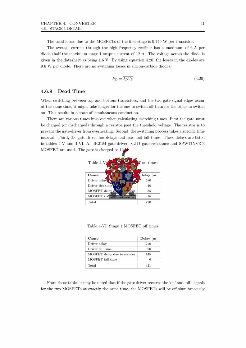
CHAPTER 4. CONVERTER 414.6. STAGE 1 DETAIL
The total losses due to the MOSFETs of the first stage is 9.749 W per transistor.The average current through the high frequency rectifier has a maximum of 6 A per
diode (half the maximum stage 1 output current of 12 A. The voltage across the diode isgiven in the datasheet as being 1.6 V. By using equation 4.20, the losses in the diodes are9.6 W per diode. There are no switching losses in silicon-carbide diodes.
PD = IDVD (4.20)
4.6.9 Dead Time
When switching between top and bottom transistors, and the two gate-signal edges occurat the same time, it might take longer for the one to switch off than for the other to switchon. This results in a state of simultaneous conduction.
There are various times involved when calculating switching times. First the gate mustbe charged (or discharged) through a resistor past the threshold voltage. The resistor is toprevent the gate-driver from overheating. Second, the switching process takes a specific timeinterval. Third, the gate-driver has delays and rise- and fall times. These delays are listedin tables 4-V and 4-VI. An IR2184 gate-driver, 8.2 Ω gate resistance and SPW17N80C3MOSFET are used. The gate is charged to 12 V.
Table 4-V: Stage 1 MOSFET on times
Cause Delay [ns]
Driver delay 680
Driver rise time 40
MOSFET delay due to resistor 35
MOSFET rise time 15
Total 770
Table 4-VI: Stage 1 MOSFET off times
Cause Delay [ns]
Driver delay 270
Driver fall time 20
MOSFET delay due to resistor 145
MOSFET fall time 6
Total 441
From these tables it may be noted that if the gate driver receives the ‘on’ and ‘off’ signalsfor the two MOSFETs at exactly the same time, the MOSFETs will be off simultaneously
CHAPTER 4. CONVERTER 424.7. TRANSFORMER DETAIL
for 329 ns. This driver-MOSFET combination therefore provides an intrinsic dead time of329 ns.
This means that the output is floating for a short period of time. This has various effects,depending on the topology and application. For the full-bridge topology designed, the effectis negligible. The reason for this is that the current stored in the leakage inductance ensuresthat the next ‘switching state’ is reached the moment the relevant switch opens (441 nsafter the gate signal edge). The voltage over the closing switch is already zero by the timeit closes.
This above argument is valid when the discharge time of the leakage inductance is largerthan the dead time. When the discharge time is smaller than the dead time (this is true whenswitching a small current from a zero state to a cross-conducting state) the reverse-recoverytime of the internal diode in the MOSFET is sufficient to recharge the leakage inductancein the opposite direction. Since the switch has not yet closed, the newly stored currentfinds a path through the original MOSFET diode, making the voltage over the transformerzero once more. The situation therefore changes from zero-voltage switching to low-currentswitching. The pulse width increases by the dead time as opposed to the leakage inductancedischarge time.
4.7 Transformer Detail
4.7.1 Configuration
Configuration of the transformer can play a major role in its performance. There are variousoptions, compared in table 4-VII.
A major concern is the leakage-inductance, due to the high frequency. Another is thephysical size of the transformer, which must fit into a 19′′ rack together with all the inductors,heat sinks, printed circuit boards and other components.
A twisted-pair transformer can be used only for a winding ratio of 1:1. The desiredwinding ratio is 45:40, which is very close to 1:1. If the diodes were to be replaced withones that has a breakdown voltage of 800V, a twisted-pair transformer would be the idealoption. This would be done in the final product. The prototype used a co-axial transformer.A twisted-pair transformer was built for comparison. The design presented further in thischapter is for a twisted-pair transformer.
Ferrite is used so that core losses are minimised at the high frequency concerned.Maximum flux density is designed as 200 mT. Using equation 4.21, the minimum numberof turns that would guarantee that the core will not saturate was calculated as 21. Thisis for a switching frequency (fs) of 47.684 kHz, a core area (Acore) of 1320 mm2 and a busvoltage (Vbus) of 566 V.
N =Vbus
2BmaxAcorefs(4.21)
It is also required that the magnetising current be limited. A magnetising current of
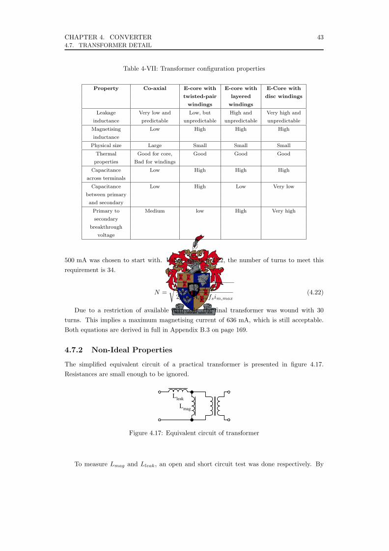
CHAPTER 4. CONVERTER 434.7. TRANSFORMER DETAIL
Table 4-VII: Transformer configuration properties
Property Co-axial E-core with E-core with E-Core with
twisted-pair layered disc windings
windings windings
Leakage Very low and Low, but High and Very high and
inductance predictable unpredictable unpredictable unpredictable
Magnetising Low High High High
inductance
Physical size Large Small Small Small
Thermal Good for core, Good Good Good
properties Bad for windings
Capacitance Low High High High
across terminals
Capacitance Low High Low Very low
between primary
and secondary
Primary to Medium low High Very high
secondary
breakthrough
voltage
500 mA was chosen to start with. Using equation 4.22, the number of turns to meet thisrequirement is 34.
N =
√Vbuslcore
2µrµ0Acorefsim,max(4.22)
Due to a restriction of available materials, the final transformer was wound with 30turns. This implies a maximum magnetising current of 636 mA, which is still acceptable.Both equations are derived in full in Appendix B.3 on page 169.
4.7.2 Non-Ideal Properties
The simplified equivalent circuit of a practical transformer is presented in figure 4.17.Resistances are small enough to be ignored.
Chapter 4 – Converter : Transformer 41
The final transformer was wound onto a ferrite E-core with a twisted-pair configuration. Ferrite
is used so that core losses are minimised at the high frequency concerned. Maximum flux-density is
designed as 200mT. Using formula 4.16, the number of turns was calculated as 21. This is for a
switching frequency (fs) of 48kHz, a core area (Acore) of 1320mm2 and a bus voltage (Vbus) of 560V.
score
bus
fABVN
max2= (4.16)
It is also required that the magnetising current be limited. A magnetising current of 500mA was
chosen. Using formula 4.17, the number of turns to meet this requirement is 34.
max,02 mscorer
corebus
ifAlVN
µµ= (4.17)
For convenience (available wire thickness, etc.), the final transformer was wound with 30 turns.
This implies a maximum magnetising current of 636mA, which is still acceptable. Both formulae are
derived in full in Appendix B.
4.8.3 Non-Ideal Properties The simplified equivalent circuit of a practical transformer is presented in figure 4.26.
Resistances are small enough to be ignored.
Lleak
Lmag
Figure 4.26 – Practical transformer
To measure Lmag and Lleak, an open- and short-circuit test was done respectively. By leaving the
secondary as an open-circuit, the ideal transformer becomes an open-circuit itself. The measurement
thus provides the combination of the two inductances. Since Lmag is much larger than Lleak, the
measurement represents Lmag. Next, by short-circuiting the secondary, the ideal transformer forms a
short-circuit over Lmag, leaving only Lleak in the measurement.
In order to perform the measurement, the transformer is driven with a square-wave using a 50Ω
signal generator. By substituting the measured half-time (t½) into equation 4.18, Lmag and Lleak were
calculated to be 2.8mH and 4µH respectively. Half-time may be defined as the time taken for the
voltage over the inductor to decrease by half the peak value. In the equation, ‘R’ is 50Ω. A co-axial
transformer, mentioned earlier, has a leakage inductance of 38µH.
)2ln(2
1 RtL = (4.18)
Figure 4.17: Equivalent circuit of transformer
To measure Lmag and Lleak, an open and short circuit test was done respectively. By

CHAPTER 4. CONVERTER 444.7. TRANSFORMER DETAIL
leaving the secondary as an open circuit, the ideal transformer becomes an open circuit.The measurement thus provides the combination of the two inductances. Since Lmag ismuch larger than Lleak, the measurement represents Lmag. Next, by short circuiting thesecondary, the ideal transformer forms a short circuit across Lmag, leaving only Lleak in themeasurement.
In order to perform the measurement, the transformer is driven with a square wave usinga 50 Ω signal generator. By substituting the measured half time (t1/2) into equation 4.23,Lmag and Lleak were calculated to be 2.8 mH and 4 µH respectively. In the equation, R is50 Ω. The co-axial transformer has a leakage inductance of 38 µH.
L =t1/2R
ln(2)(4.23)
Another high-frequency consideration is the effect of skin-depth, given by equation 4.24.At the switching frequency of 47.684 kHz, the skin-depth of copper is 0.3 mm. If the 10th
harmonic of the square wave is still considered, the skin-depth is 0.1 mm.
δ =√
2ρ
ωµ(4.24)
The ideal would thus be to wind the transformer with strands of 100 µm diameter in orderto minimise the effective resistance and thus increase efficiency. The prototype transformerwas wound with two strands of 1.2 mm diameter copper wire in order to save time.
4.7.3 Leakage Inductance
When using a full-bridge topology, as in stage 1, the duty-cycle error is only dependant onthe output current (a slow-changing property) and not on the specific timing. Equation4.25 provides the discharge time as a function of switched current (equal to the first stageinductor current). This is the time it takes the transformer secondary to rise after theopening switch has switched off.
t =2iLleak
Vbus(4.25)
The maximum switched current is 12 A and the bus voltage is 566 V. The twistedpair transformer and the co-axial transformer has maximum discharge times of 170 ns and1.611 µs respectively. The associated duty-cycle errors are 0.81% and 7.7% respectively.These are quoted as absolute errors, not relative errors.
4.7.4 Isolation
Isolation across the transformer is an important consideration. Standard resin-coatedtransformer wire has an electrical breakdown voltage of approximately 1 kV and must notbe exceeded. Figure 4.18a shows the line voltages relative to neutral (or ground, assumingthat neutral and ground are at the same potential). Figure 4.18b shown the output of the
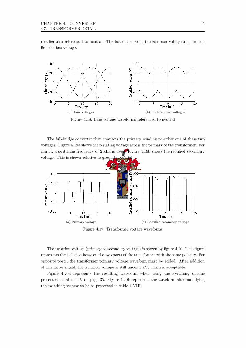
CHAPTER 4. CONVERTER 454.7. TRANSFORMER DETAIL
rectifier also referenced to neutral. The bottom curve is the common voltage and the topline the bus voltage.
(a) Line voltages (b) Rectified line voltages
Figure 4.18: Line voltage waveforms referenced to neutral
The full-bridge converter then connects the primary winding to either one of these twovoltages. Figure 4.19a shows the resulting voltage across the primary of the transformer. Forclarity, a switching frequency of 2 kHz is used. Figure 4.19b shows the rectified secondaryvoltage. This is shown relative to ground potential.
(a) Primary voltage (b) Rectified secondary voltage
Figure 4.19: Transformer voltage waveforms
The isolation voltage (primary to secondary voltage) is shown by figure 4.20. This figurerepresents the isolation between the two ports of the transformer with the same polarity. Foropposite ports, the transformer primary voltage waveform must be added. After additionof this latter signal, the isolation voltage is still under 1 kV, which is acceptable.
Figure 4.20a represents the resulting waveform when using the switching schemepresented in table 4-IV on page 35. Figure 4.20b represents the waveform after modifyingthe switching scheme to be as presented in table 4-VIII.

CHAPTER 4. CONVERTER 464.7. TRANSFORMER DETAIL
(a) Standard switching cycle (b) Modified switching cycle
Figure 4.20: Isolation voltage waveforms
Table 4-VIII: Switching sequence
State S1 S2 S3 S4 Condition
A 1 0 0 1 Cross-conducting
B 0 1 0 1 Zero
C 0 1 1 0 Cross-conducting
D 0 1 0 1 Zero
There are many advantages to this scheme. One advantage is the elimination of a high-frequency component over the transformer isolation boundary. Another is that standardhalf-bridge switching signals may be used, which allows for an easy upgrade from half-bridgeto full-bridge by simply changing the MOSFET Drivers. The operation of the circuit is notaffected. The only consideration is the fact that the two bottom switches carry currentfor longer periods than the top switches, as opposed to the balanced situation observedpreviously.
4.7.5 Thermal Analysis
Both the primary and the secondary used 4.8 m of 2.26 mm2 copper wire. The resistanceof each winding is given by equation 4.26, where R is the resistance, ρ the resistivity, l thelength and A the cross-sectional area. The resulting resistance of each winding is 35.64 mΩ.
R =ρl
A(4.26)
At an rms current of 6 A, the total loss in both windings is 2.566 W. This is very smallconsidering the relatively large surface area of the transformer. This calculation does nottake skin-effect into account.
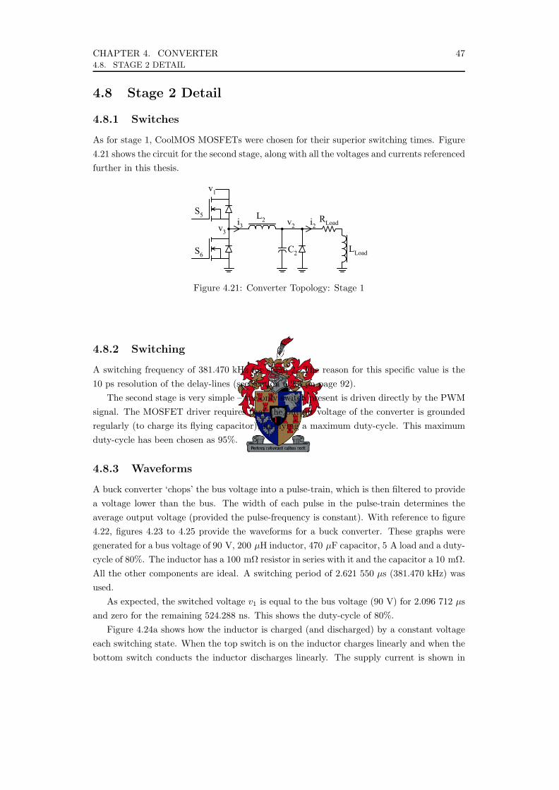
CHAPTER 4. CONVERTER 474.8. STAGE 2 DETAIL
4.8 Stage 2 Detail
4.8.1 Switches
As for stage 1, CoolMOS MOSFETs were chosen for their superior switching times. Figure4.21 shows the circuit for the second stage, along with all the voltages and currents referencedfurther in this thesis.
Chapter 1 – Converter : Summary 29
The copper thickness on the power PCB is 70µm. This means that a conductor carrying 15A
must be 8mm wide. Similarly, a 6A track must be 2mm and a 12A track 6mm. These widths have been
calculated using the “Track Amp Calculator” from North Tech Services (http://www.ntspcb.co.za). A
temperature difference of 10°C has been assumed.
1.13 Summary After considering the requirements, a two-stage topology has been chosen. The two stages are
implemented as an isolated full-bridge (figure 4.28) and a buck converter (figure 4.29) respectively.
A B C
Neutral
S1
S2
T1
S3
S4
L1
C1
i1v1
560V
Figure 1.28 – Converter Topology: Stage 1
RLoad
LLoad
L2S5
v2 i2
v1
v3i3
C2S6
Figure 1.29 – Converter Topology: Stage 2
The bus capacitor was designed as two 470µF, 400V capacitors in series. Both filter capacitors
are the same 400V, 470µF capacitors. The filter inductors L1 and L2 were calculated to be 3mH and
200µH respectively. Their physical construction was provided.
The transformer has been designed with a 1:1 winding ration and twisted-pair windings. The
leakage inductance was measured as 4µH and the effect has been studied. The dead-time of 500ns was
found to remove the effect of leakage inductance.
Furthermore, the soft-start sequence has been chosen. The two duty-cycles, D1 and D2, are to be
ramped to 13% and 80%, respectively, in 2s. After this the control system may take over.
The total losses of the components to be bolted to the heat-sink were calculated as 70W. A fan
would thus need to be included as part of the casing.
Figure 4.21: Converter Topology: Stage 1
4.8.2 Switching
A switching frequency of 381.470 kHz for stage 2. The reason for this specific value is the10 ps resolution of the delay-lines (see section 6.2.3 on page 92).
The second stage is very simple – the only switch present is driven directly by the PWMsignal. The MOSFET driver requires that the output voltage of the converter is groundedregularly (to charge its flying capacitor), implying a maximum duty-cycle. This maximumduty-cycle has been chosen as 95%.
4.8.3 Waveforms
A buck converter ‘chops’ the bus voltage into a pulse-train, which is then filtered to providea voltage lower than the bus. The width of each pulse in the pulse-train determines theaverage output voltage (provided the pulse-frequency is constant). With reference to figure4.22, figures 4.23 to 4.25 provide the waveforms for a buck converter. These graphs weregenerated for a bus voltage of 90 V, 200 µH inductor, 470 µF capacitor, 5 A load and a duty-cycle of 80%. The inductor has a 100 mΩ resistor in series with it and the capacitor a 10 mΩ.All the other components are ideal. A switching period of 2.621 550 µs (381.470 kHz) wasused.
As expected, the switched voltage v1 is equal to the bus voltage (90 V) for 2.096 712 µsand zero for the remaining 524.288 ns. This shows the duty-cycle of 80%.
Figure 4.24a shows how the inductor is charged (and discharged) by a constant voltageeach switching state. When the top switch is on the inductor charges linearly and when thebottom switch conducts the inductor discharges linearly. The supply current is shown in

CHAPTER 4. CONVERTER 484.8. STAGE 2 DETAIL
Chapter 1 – Converter : Wave-Forms 15
1.6.3 Stage 2 A buck converter ‘chops’ the bus voltage into a pulse-train, which is then filtered to provide a
voltage lower than the bus. The width of each pulse in the pulse-train determines the average output
voltage (provided the pulse-frequency is constant). With reference to figure 4.19, figures 4.20 to 4.24
provide the wave-forms for a buck converter.
vbus
is
v1
vC
iCiLoad
iL
Figure 1.19 – Buck converter wave-forms: circuit
Figure 1.20 – Buck converter wave-forms: is
Figure 1.21 – Buck converter wave-forms: v1
Figure 4.22: Buck converter waveforms: circuit
Figure 4.23: Buck converter waveforms: Switched voltage
(a) Inductor current (b) Supply current
Figure 4.24: Buck converter waveforms
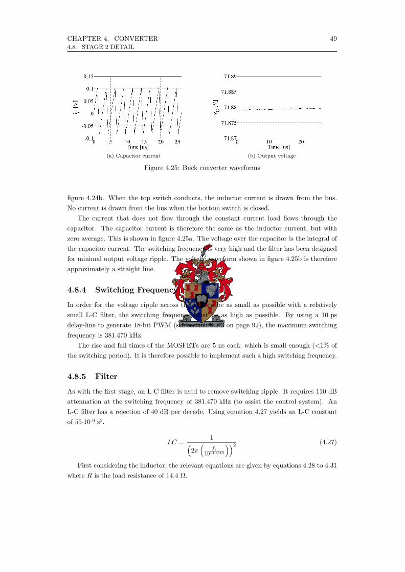
CHAPTER 4. CONVERTER 494.8. STAGE 2 DETAIL
(a) Capacitor current (b) Output voltage
Figure 4.25: Buck converter waveforms
figure 4.24b. When the top switch conducts, the inductor current is drawn from the bus.No current is drawn from the bus when the bottom switch is closed.
The current that does not flow through the constant current load flows through thecapacitor. The capacitor current is therefore the same as the inductor current, but withzero average. This is shown in figure 4.25a. The voltage over the capacitor is the integral ofthe capacitor current. The switching frequency is very high and the filter has been designedfor minimal output voltage ripple. The voltage waveform shown in figure 4.25b is thereforeapproximately a straight line.
4.8.4 Switching Frequency
In order for the voltage ripple across the load to be as small as possible with a relativelysmall L-C filter, the switching frequency must be as high as possible. By using a 10 psdelay-line to generate 18-bit PWM (see section 6.2.3 on page 92), the maximum switchingfrequency is 381.470 kHz.
The rise and fall times of the MOSFETs are 5 ns each, which is small enough (<1% ofthe switching period). It is therefore possible to implement such a high switching frequency.
4.8.5 Filter
As with the first stage, an L-C filter is used to remove switching ripple. It requires 110 dBattenuation at the switching frequency of 381.470 kHz (to assist the control system). AnL-C filter has a rejection of 40 dB per decade. Using equation 4.27 yields an L-C constantof 55·10-9 s2.
LC =1(
2π(
fs
10110/40
))2 (4.27)
First considering the inductor, the relevant equations are given by equations 4.28 to 4.31where R is the load resistance of 14.4 Ω.
CHAPTER 4. CONVERTER 504.8. STAGE 2 DETAIL
L =(vbus − vout)D
∆ifs(4.28)
vbus =vout
D(4.29)
D = 0.8 (4.30)
L =0.2Riout
∆ifs(4.31)
The inductor must thus be 113 µH for a ripple current of smaller than 1 A. Furthermore,with a 470 µF capacitor, the inductor needs to be 117 µH to adequately remove the switchingvoltage ripple. A 200 µH inductor was chosen.
Using the same design-procedure as in stage 1 (section 4.6.7), 21 turns were wound rounda 1056 mm2 laminated-steel E-core. The air-gap was chosen to be 1.5 mm (3 mm total).
4.8.6 Losses
During steady state conditions, the inductor current is always positive. This implies that thetop MOSFET operates under hard-switching conditions for both the ‘on’ and ‘off’ transients.This also means that the bottom MOSFET operates under zero-voltage switching for bothtransients. The switching loss for the bottom MOSFET is thus zero, but for the top one isgiven by equation 4.32.
Ps = (trise + tfall) v1i3fs (4.32)
In equation 4.32, Ps is the switching losses and trise and tfall the rise and fall times of theMOSFET respectively. The switching frequency fs is 381.470 kHz. The inductor current i3
has a maximum value of 15 A. The input voltage v1 has a maximum steady-state value of270 V (14.4 Ω · 15 A · 1.25).
Different MOSFETs (IPW60R099CP, Infineon) are utilised for stage 2. These MOSFETshave an ‘on’ resistance of 99 mΩ and rise and fall times of 5 ns each. The resulting switchingloss for the top MOSFET is therefore 15.45 W.
Conduction losses are taken at a duty-cycle of 80%. The maximum rms current throughthe top MOSFET can thus be approximated as 12 A. Similarly the maximum rms currentthrough the bottom MOSFET can be approximated as 3 A. This is valid for a very smallinductor current ripple. The conduction losses are thus 14.256 W for the top transistor and891 mW for the bottom one. Total losses are 29.706 W for the top transistor and 891 mWfor the bottom one.

CHAPTER 4. CONVERTER 514.9. HEATSINK
4.8.7 Dead Time
As discussed in section 4.6.9, there has to be a time between switching the one transistoroff and the other one on. This time is called the dead time.
The MOSFETs used in the second stage converter are faster than those used in the firststage. A similar calculation can be performed as in tables 4-V and 4-VI on page 41. Thedelays applicable for stage 2 are listed in tables 4-IX and 4-X. An IR2181 gate-driver, 8.2 Ωgate resistance and IPW60R099CP MOSFET are used. The gate is charged to 12 V.
Table 4-IX: Stage 2 MOSFET on times
Cause Delay [ns]
Driver delay 180
Driver rise time 40
MOSFET delay due to resistor 20
MOSFET rise time 5
Total 245
Table 4-X: Stage 2 MOSFET off times
Cause Delay [ns]
Driver delay 220
Driver fall time 20
MOSFET delay due to resistor 172
MOSFET fall time 5
Total 417
The externally applied dead time must therefore be more than 172 ns, which correspondsto a duty-cycle of 6.56% at a switching frequency of 381.470 kHz. The signal for the topswitch remains unadjusted. The signal for the bottom switch rises late and falls early. Thisis so that the top switch duty cycle is exactly as it would have been for a standard buckconverter (with a diode in the place of the bottom switch).
4.9 Heatsink
4.9.1 Contribution of Stage 1 MOSFETS
In section 4.6.8 the total losses have been calculated as 9.749 W per transistor. The total istherefore 39 W for the four MOSFETS.

CHAPTER 4. CONVERTER 524.9. HEATSINK
According to the datasheet, the junction to case thermal resistance θJC of the MOSFETsis given as 0.6 K·W-1. By using eqation 4.33 [6], the maximum case temperature TC can becalculated.
TC = TJ − PθJC (4.33)
The maximum junction temperature TJ is given by the datasheet as 150 C. This impliesa maximum case temperature of 140 C.
The thermal resistance of the pads used to isolate the heatsink from the MOSFETs havea thermal resistance of 0.4 K·W-1. The temperature of the heatsink at the MOSFET TH
must therefore be lower than 136 C.
4.9.2 Contribution of Stage 1 Diodes
In section 4.6.8 the total losses have been calculated as 9.6 W per diode. The total istherefore 38.4 W for the four diodes.
According to the datasheet, the junction to case thermal resistance of the diodes is givenas 2.6 K·W-1. The maximum junction temperature is given by the datasheet as 175 C.This implies a maximum case temperature of 150 C.
The thermal resistance of the pads used to isolate the heatsink from the MOSFETshave a thermal resistance of 0.4 K·W-1. The temperature of the heatsink at the diode musttherefore be lower than 146 C.
4.9.3 Contribution of Stage 2 MOSFETS
In section 4.8.6 the losses for the top and bottom MOSFET has been calculated as 29.706 Wand 891 mW respectively.
According to the datasheet, the junction to case thermal resistance θJC of the MOSFETsis given as 0.5 K·W-1. The maximum junction temperature is given by the datasheet as150 C. This implies a maximum case temperature for the top and bottom MOSFET of135 C and 149.55 C respectively.
The thermal resistance of the pads used to isolate the heatsink from the MOSFETs havea thermal resistance of 0.4 K·W-1. The temperature of the heatsink at the MOSFET musttherefore be lower than 123 C for the top MOSFET and 149.2 C for the bottom one.
4.9.4 The Required Heatsink
All the above components are to be mounted onto the same heatsink. The temperature ofthat heatsink must be kept lower than 123 C. The total power dissipation is 117.742 W.Assuming a maximum ambient of 45 C, the thermal resistance of the heatsink must besmaller than 0.6625 K·W-1
According to the datasheet, a natural-convection SK109 heatsink from Fischer Elektronikthat is 200 mm long has a thermal resistance of 0.6 K·W-1. When mounted horizontally and
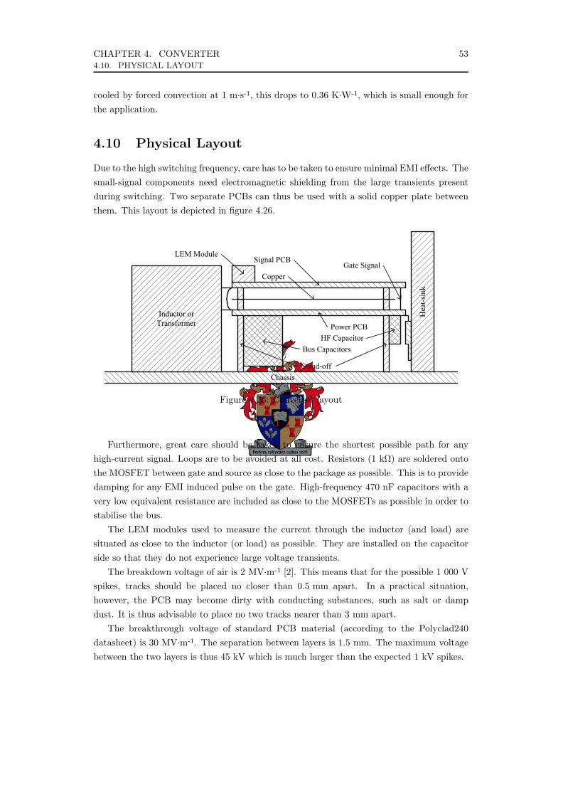
CHAPTER 4. CONVERTER 534.10. PHYSICAL LAYOUT
cooled by forced convection at 1 m·s-1, this drops to 0.36 K·W-1, which is small enough forthe application.
4.10 Physical Layout
Due to the high switching frequency, care has to be taken to ensure minimal EMI effects. Thesmall-signal components need electromagnetic shielding from the large transients presentduring switching. Two separate PCBs can thus be used with a solid copper plate betweenthem. This layout is depicted in figure 4.26.
Chapter 4 – Converter : Physical Layout 49
4.12 Physical Layout Due to the high switching frequency, care has to be taken to ensure minimal EMI effects. The
small-signal components need electro-magnetic shielding from the large transients present during
switching. Two separate PCBs can thus be used with a solid copper plate between them. This layout is
depicted in figure 4.27.
Chassis
Hea
t-sin
k
Inductor orTransformer
Stand-off
Power PCB
Signal PCB
CopperGate Signal
HF CapacitorBus Capacitors
LEM Module
Figure 4.27 – Converter layout
Furthermore, great care should be taken to ensure the shortest possible path for any high-current
signal. Loops are to be avoided at all cost. Resistors (1kΩ) are soldered onto the MOSFET between
gate and source as close to the package as possible. This is to provide damping for any EMI induced
pulse on the gate. High-frequency 470nF capacitors with a very low equivalent resistance are included
as close to the MOSFETs as possible in order to stabilise the bus.
The LEM modules used to measure the current through the inductor (and load) are situated as
close to the inductor (or load) as possible. They are installed on the capacitor side so that they do not
experience large voltage transients.
The breakdown voltage of air is 2MV·m-1. This means that for the possible 1000V spikes, tracks
should be placed no nearer than 0.5mm apart. In a practical situation, however, the PCB may become
dirty with conducting substances, such as salt or damp dust. It is thus advisable to place no two tracks
nearer than 3mm apart.
The breakthrough voltage of standard PCB material is 30MV·m-1. The separation between layers
is 1.5mm. The maximum voltage between the two layers is thus 45kV, which is much larger than the
expected 1kV spikes.
Figure 4.26: Converter layout
Furthermore, great care should be taken to ensure the shortest possible path for anyhigh-current signal. Loops are to be avoided at all cost. Resistors (1 kΩ) are soldered ontothe MOSFET between gate and source as close to the package as possible. This is to providedamping for any EMI induced pulse on the gate. High-frequency 470 nF capacitors with avery low equivalent resistance are included as close to the MOSFETs as possible in order tostabilise the bus.
The LEM modules used to measure the current through the inductor (and load) aresituated as close to the inductor (or load) as possible. They are installed on the capacitorside so that they do not experience large voltage transients.
The breakdown voltage of air is 2 MV·m-1 [2]. This means that for the possible 1 000 Vspikes, tracks should be placed no closer than 0.5 mm apart. In a practical situation,however, the PCB may become dirty with conducting substances, such as salt or dampdust. It is thus advisable to place no two tracks nearer than 3 mm apart.
The breakthrough voltage of standard PCB material (according to the Polyclad240datasheet) is 30 MV·m-1. The separation between layers is 1.5 mm. The maximum voltagebetween the two layers is thus 45 kV which is much larger than the expected 1 kV spikes.

CHAPTER 4. CONVERTER 544.11. SUMMARY
The copper thickness on the power PCB is 70 µm. This means that a conductor carrying15 A must be 8 mm wide. Similarly, a 6 A track must be 2 mm and a 12 A track 6 mm.These widths have been calculated using the “Track Amp Calculator” from North TechServices (http://www.ntspcb.co.za). A temperature difference of 10 C was assumed.
4.11 Summary
After considering the requirements, a two-stage topology was chosen. The two stages areimplemented as an isolated full-bridge (figure 4.10) and a synchronous buck converter (figure4.21) respectively.
The bus capacitor was designed as two 470 µF, 400 V capacitors in series. Both filtercapacitors are the same 400 V, 470 µF capacitors. The filter inductors L1 and L2 werecalculated to be 3 mH and 200 µH respectively. Their physical construction was provided.
The transformer was designed with a 1:1 winding ratio and twisted-pair windings. Theuse of this transformer is valid if the high frequency rectifier diodes are replaced with diodesthat can withstand 800 V.
The leakage inductance was measured as 4 µH and the effect was studied.The total losses of the components to be bolted to the heat sink were calculated as
118 W. A fan would thus need to be included as part of the casing.
Chapter 5
Control System
5.1 Introduction
In chapter 4 the converter was designed. The next component on the list is the controlsystem. This chapter includes all aspects of the control system implemented for theconverter. It starts with a discussion and mathematical model of the system to be controlled.
Next, different control strategies are presented, along with block diagrams. The finalcontrol system is designed using continuous time design methods. The measurements taken,along with their respective accuracy and precision, are then considered. Simulation resultsare presented. The implementation of the control system in firmware is presented anddiscussed.
Throughout this chapter, reference is made to signals and components of the converter.Figures 4.10 on page 34 and 4.21 on page 47 show the circuit diagrams of both stages, alongwith all the signals referenced in this chapter. The duty-cycle of the first stage is D1 andthat of the second stage D2.
5.2 Specification
5.2.1 Range
The converter output voltage range was specified in section 4.3.4 on page 24 as 0 V to 250 V.The converter output current range is 0 A to 15 A.
Similarly, the stage 1 output voltage range is 0 V to 312.5 V. The stage 1 output currentrange is 0 A to 12 A.
5.2.2 Bandwidth
The load is characterised by an inductance of 15 H and a series resistance of 14.4 Ω. Thetime-constant τ of this load is thus 1.11 s (equation 5.1). This corresponds to a bandwidthβ of 153 mHz (equation 5.2).
55

CHAPTER 5. CONTROL SYSTEM 565.2. SPECIFICATION
The settling time of the output current i2 is specified as 5 s upon any step input.Equation 5.3 shows a simple 1st order response to a unity step where τ is the systemtime-constant and y the output.
τ =L
R(5.1)
β =1
2πτ(5.2)
y = 1− e−t/τ (5.3)
By finding the error between y and unity, the desired 10 ppm level is reached after11.5·τ . As this calculation assumes that the load is uncharged at time zero, it represents theworst case scenario. The closed-loop time constant must thus be smaller than 435 ms. Thiscorresponds to a bandwidth of 366 mHz. Compensating for effects due to the high order ofthe system and practical shortcomings, a closed-loop bandwidth of 1 Hz was chosen.
5.2.3 Accuracy
The accuracy of the current source is dependant on, among others, the accuracy ofmeasurement. Say, for example, the control system is given a 1 A reference. It measuresthe output as being 1 A. There would therefore seem to be no error. The reality is that themeasurement of the output current is 5% in error with respect to the absolute value. Sucha system would then have an accuracy of 5%.
The specified accuracy of the system is 10 ppm.
5.2.4 Stability
The stability of the system is specified as 10 ppm. This means that the output current ofthe converter may not drift more than 10 ppm. It also means that the output current ripplemay not be larger than 10 ppm.
5.2.5 Resolution
The stability of the system has been specified as 10 ppm. At minimum load (1 A), this is10 µA, corresponding to a magnetic flux density resolution of 800 nT The specification inappendix A requires a resolution of 1 µT, which would imply that it is possible to implement- given that the stability of 10 ppm was reached.
A resolution on 1 µT with a range of 1.2 T would imply a reference word 24 bits wide.

CHAPTER 5. CONTROL SYSTEM 575.3. BLOCK DIAGRAMS
5.3 Block Diagrams
5.3.1 System Diagram
The initial aspect to consider is whether to control the system as a whole, or to link the twoseparate control systems by using stage 2 to drive stage 1’s reference. By making stage 1react at least ten times faster than stage 2 it is possible to control them separately.
This is convenient for the implementation of feed-forward. Feed-forward is the methodof choice in many existing implementations [3; 9; 12]. The control system for stage 2 canspecify the voltage it requires at the input of its filter (v3). The control system for stage1 can then ensure that the required stage 2 duty-cycle is approximately 80%. The exactduty-cycle is then calculated by the feed-forward implementation. Figure 5.1 shows the fullcontrol system block diagram, containing all the aspects discussed earlier. More detail abouteach block is presented in the following sub-sections.
Chapter 5 – Control System : Block Diagrams 52
5.1 Block Diagrams 5.1.1 System Diagram
The initial aspect to consider is whether to control the system as a whole, or to link the two
separate control systems by using stage 2 to drive stage 1’s reference. By making stage 1 react at least
ten times faster than stage 2 it is possible to control them separately.
This is convenient for the implementation of feed-forward. The control system for stage 2 can
specify the voltage it requires at the input of its filter (v3). The control system for stage 1 can then
ensure that the required stage 2 duty-cycle is approximately 80%. The exact duty-cycle is then
calculated by the feed-forward implementation. Figure 5.3 shows the full control system block
diagram, containing all the aspects discussed earlier. More detail about each block is presented in the
following sub-sections.
Estimator Stage 2Stage 1
1.25i2,ref
i2
i1i3
v1v2 v3
i2
v2
v1 D2
D1
refref
x1
Figure 5.3 – Control system block diagram
5.1.2 Stage 1 Many different control strategies exist for an isolated full-bridge topology, the simplest of which
is when voltage is fed back to the PWM generator with a lead-lag network for stability [17]. This is
depicted in figure 5.4. The lead-lag network may also be replaced with a proportional-integral (PI)
controller [1], [31].
L-C FilterPWMLead-lagnetworkvref vout
Figure 5.4 – Voltage control
Figure 5.1: Control system block diagram
5.3.2 Stage 1
Many different control strategies exist for an isolated full-bridge topology, the simplestof which is when voltage is fed back to the PWM generator with a lead-lag network forstability [6]. This is depicted in figure 5.2. The lead-lag network may also be replaced witha proportional-integral (PI) controller [11; 12].
Chapter 5 – Control System : Block Diagrams 52
5.1 Block Diagrams 5.1.1 System Diagram
The initial aspect to consider is whether to control the system as a whole, or to link the two
separate control systems by using stage 2 to drive stage 1’s reference. By making stage 1 react at least
ten times faster than stage 2 it is possible to control them separately.
This is convenient for the implementation of feed-forward. The control system for stage 2 can
specify the voltage it requires at the input of its filter (v3). The control system for stage 1 can then
ensure that the required stage 2 duty-cycle is approximately 80%. The exact duty-cycle is then
calculated by the feed-forward implementation. Figure 5.3 shows the full control system block
diagram, containing all the aspects discussed earlier. More detail about each block is presented in the
following sub-sections.
Estimator Stage 2Stage 1
1.25i2,ref
i2
i1i3
v1v2 v3
i2
v2
v1 D2
D1
refref
x1
Figure 5.3 – Control system block diagram
5.1.2 Stage 1 Many different control strategies exist for an isolated full-bridge topology, the simplest of which
is when voltage is fed back to the PWM generator with a lead-lag network for stability [17]. This is
depicted in figure 5.4. The lead-lag network may also be replaced with a proportional-integral (PI)
controller [1], [31].
L-C FilterPWMLead-lagnetworkvref vout
Figure 5.4 – Voltage control Figure 5.2: Voltage control
More commonly used is a fast current-feedback inner-loop (usually hysteresis control)with a slower voltage-feedback outer-loop [3]. This is presented in figure 5.3. The greatest
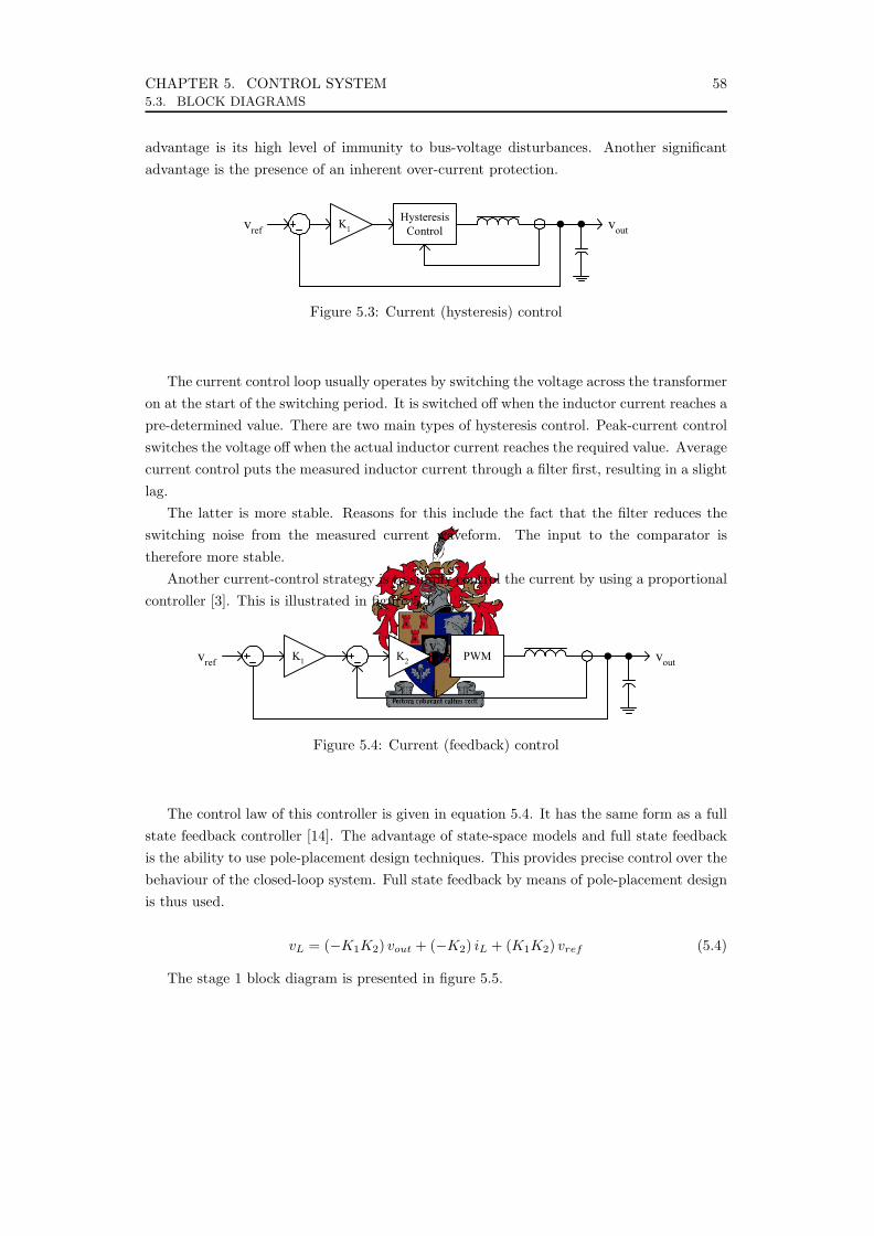
CHAPTER 5. CONTROL SYSTEM 585.3. BLOCK DIAGRAMS
advantage is its high level of immunity to bus-voltage disturbances. Another significantadvantage is the presence of an inherent over-current protection.
Chapter 5 – Control System : Block Diagrams 53
More commonly used, however, is a fast current-feedback inner-loop (usually hysteresis control)
with a slower voltage-feedback outer-loop [9]. This is presented in figure 5.5. The greatest advantage
is its high level of immunity to bus-voltage disturbances. Another significant advantage is the presence
of an inherent over-current protection.
HysteresisControlvref voutK1
Figure 5.5 – Current (hysteresis) control
The current control loop usually operates by switching the voltage over the transformer on at the
start of the switching period. It is switched off when the inductor current reaches a pre-determined
value. There are two main types of hysteresis control. Peak-current control switches the voltage off
when the actual inductor current reaches the required value. Average current control puts the measured
inductor current through a filter first, resulting in a slight lag. The latter is more stable.
Another current-control strategy is to simply control the current by using a proportional controller
[9]. This is illustrated in figure 5.6.
vref voutK1 K2
iL
vL PWM
Figure 5.6 – Current (feedback) control
The control law of this controller is given in equation 5.1. It has the same form as a full-state
feedback controller [6]. The advantage of state-space models and full-state feedback is the ability to
use pole-placement design techniques. This provides precise control over the behaviour of the closed-
loop system. Full-state feedback by means of pole-placement is thus used.
( ) ( ) ( ) refLoutL vKKiKvKKv 21221 +−+−= (5.1)
Figure 5.3: Current (hysteresis) control
The current control loop usually operates by switching the voltage across the transformeron at the start of the switching period. It is switched off when the inductor current reaches apre-determined value. There are two main types of hysteresis control. Peak-current controlswitches the voltage off when the actual inductor current reaches the required value. Averagecurrent control puts the measured inductor current through a filter first, resulting in a slightlag.
The latter is more stable. Reasons for this include the fact that the filter reduces theswitching noise from the measured current waveform. The input to the comparator istherefore more stable.
Another current-control strategy is to simply control the current by using a proportionalcontroller [3]. This is illustrated in figure 5.4.
Chapter 5 – Control System : Block Diagrams 53
More commonly used, however, is a fast current-feedback inner-loop (usually hysteresis control)
with a slower voltage-feedback outer-loop [9]. This is presented in figure 5.5. The greatest advantage
is its high level of immunity to bus-voltage disturbances. Another significant advantage is the presence
of an inherent over-current protection.
HysteresisControlvref voutK1
Figure 5.5 – Current (hysteresis) control
The current control loop usually operates by switching the voltage over the transformer on at the
start of the switching period. It is switched off when the inductor current reaches a pre-determined
value. There are two main types of hysteresis control. Peak-current control switches the voltage off
when the actual inductor current reaches the required value. Average current control puts the measured
inductor current through a filter first, resulting in a slight lag. The latter is more stable.
Another current-control strategy is to simply control the current by using a proportional controller
[9]. This is illustrated in figure 5.6.
vref voutK1 K2
iL
vL PWM
Figure 5.6 – Current (feedback) control
The control law of this controller is given in equation 5.1. It has the same form as a full-state
feedback controller [6]. The advantage of state-space models and full-state feedback is the ability to
use pole-placement design techniques. This provides precise control over the behaviour of the closed-
loop system. Full-state feedback by means of pole-placement is thus used.
( ) ( ) ( ) refLoutL vKKiKvKKv 21221 +−+−= (5.1)
Figure 5.4: Current (feedback) control
The control law of this controller is given in equation 5.4. It has the same form as a fullstate feedback controller [14]. The advantage of state-space models and full state feedbackis the ability to use pole-placement design techniques. This provides precise control over thebehaviour of the closed-loop system. Full state feedback by means of pole-placement designis thus used.
vL = (−K1K2) vout + (−K2) iL + (K1K2) vref (5.4)
The stage 1 block diagram is presented in figure 5.5.
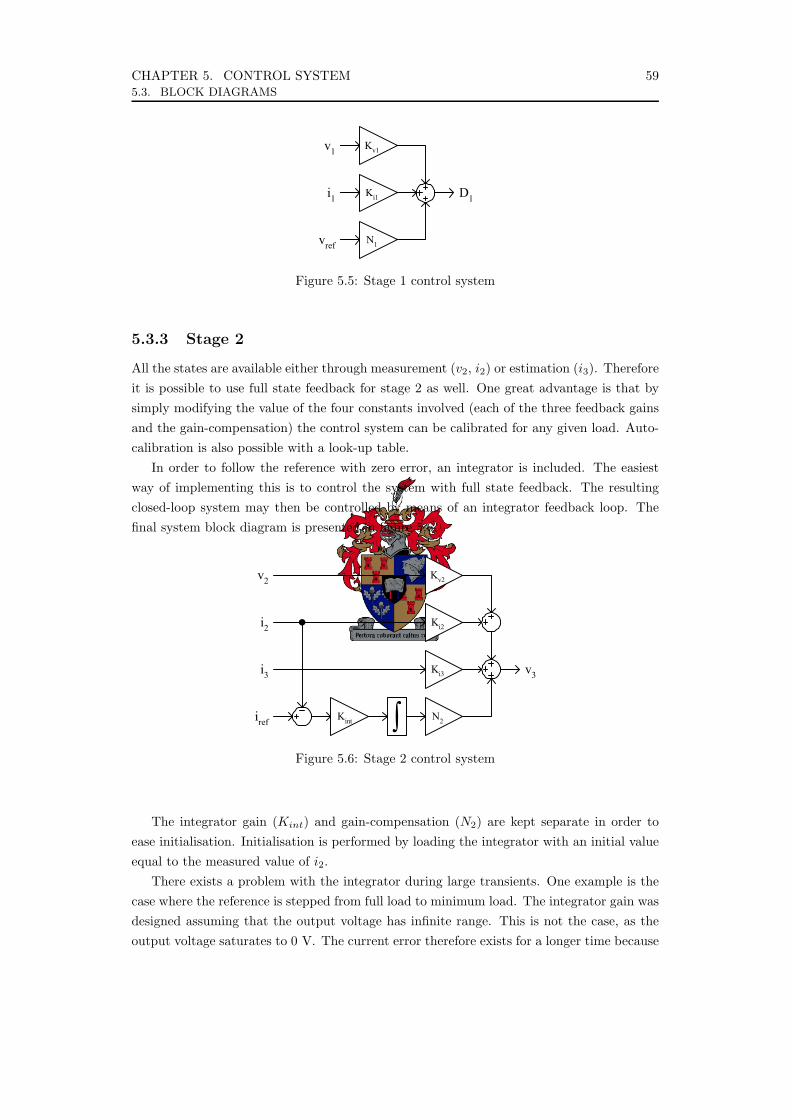
CHAPTER 5. CONTROL SYSTEM 595.3. BLOCK DIAGRAMS
Chapter 1 – Control System : Block Diagrams 4
As a final consideration, a step voltage reference results in a large current-spike through the
inductor. In the real system this would not be a problem, since the voltage reference would always be
slow (maximum 500V·s-1 according to simulation). As a precaution, however, the voltage reference is
ramp-limited to 1kV·s-1. The stage 1 block diagram is presented in figure 5.7.
Ki1
v1 Kv1
N1
i1
vref
D1
Figure 1.7 – Stage 1 control system
1.1.3 Stage 2 All the states are available either through measurement (v2, i2) or estimation (i3). Therefore it is
possible to use full-state feedback for stage 2 as well. One great advantage is that by simply modifying
the value of the four constants involved (each of the three feedback gains and the gain-compensation)
the control system can be calibrated for any given load. Auto-calibration is also possible with a look-
up table.
In order to follow the reference with zero error, an integrator is included. The easiest way of
implementing this is to control the system with full-state feedback. The resulting closed-loop system
may then be controlled by means of an integrator feedback loop.
In order to limit the voltage spike needed to charge the load inductor, another ramp-limiter is
included. It takes 1.83s for a 1Hz, single order system to settle to 10ppm (as shown earlier). The entire
system must settle in less than 5s, which leaves a remainder of just over 3s. The largest step reference
is 15A, therefore a 5A·s-1 limiter would be satisfactory. The maximum voltage is then 279.54V (as
calculated in chapter 4). The final system block diagram is presented in figure 5.8.
Ki3
i2
N2
i3
iref
v3
Ki2
Kv2
RampLimiter Kint
v2
∫
Figure 1.8 – Stage 2 control system
Figure 5.5: Stage 1 control system
5.3.3 Stage 2
All the states are available either through measurement (v2, i2) or estimation (i3). Thereforeit is possible to use full state feedback for stage 2 as well. One great advantage is that bysimply modifying the value of the four constants involved (each of the three feedback gainsand the gain-compensation) the control system can be calibrated for any given load. Auto-calibration is also possible with a look-up table.
In order to follow the reference with zero error, an integrator is included. The easiestway of implementing this is to control the system with full state feedback. The resultingclosed-loop system may then be controlled by means of an integrator feedback loop. Thefinal system block diagram is presented in figure 5.6.
Chapter 1 – Control System : Block Diagrams 4
As a final consideration, a step voltage reference results in a large current-spike through the
inductor. In the real system this would not be a problem, since the voltage reference would always be
slow (maximum 500V·s-1 according to simulation). As a precaution, however, the voltage reference is
ramp-limited to 1kV·s-1. The stage 1 block diagram is presented in figure 5.7.
Ki1
v1 Kv1
N1
i1
vref
D1
Figure 1.7 – Stage 1 control system
1.1.3 Stage 2 All the states are available either through measurement (v2, i2) or estimation (i3). Therefore it is
possible to use full-state feedback for stage 2 as well. One great advantage is that by simply modifying
the value of the four constants involved (each of the three feedback gains and the gain-compensation)
the control system can be calibrated for any given load. Auto-calibration is also possible with a look-
up table.
In order to follow the reference with zero error, an integrator is included. The easiest way of
implementing this is to control the system with full-state feedback. The resulting closed-loop system
may then be controlled by means of an integrator feedback loop.
In order to limit the voltage spike needed to charge the load inductor, another ramp-limiter is
included. It takes 1.83s for a 1Hz, single order system to settle to 10ppm (as shown earlier). The entire
system must settle in less than 5s, which leaves a remainder of just over 3s. The largest step reference
is 15A, therefore a 5A·s-1 limiter would be satisfactory. The maximum voltage is then 279.54V (as
calculated in chapter 4). The final system block diagram is presented in figure 5.8.
Ki3
i2
N2
i3
iref
v3
Ki2
Kv2
Kint
v2
∫
Figure 1.8 – Stage 2 control system Figure 5.6: Stage 2 control system
The integrator gain (Kint) and gain-compensation (N2) are kept separate in order toease initialisation. Initialisation is performed by loading the integrator with an initial valueequal to the measured value of i2.
There exists a problem with the integrator during large transients. One example is thecase where the reference is stepped from full load to minimum load. The integrator gain wasdesigned assuming that the output voltage has infinite range. This is not the case, as theoutput voltage saturates to 0 V. The current error therefore exists for a longer time because
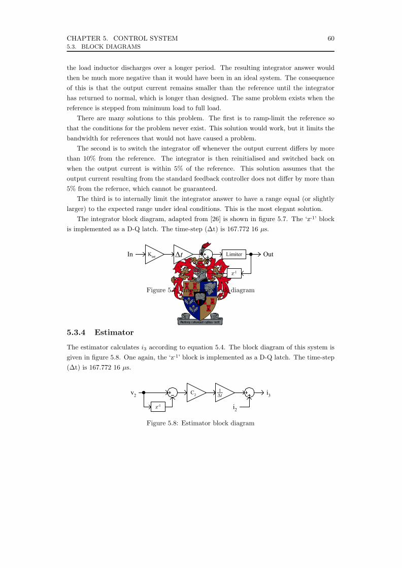
CHAPTER 5. CONTROL SYSTEM 605.3. BLOCK DIAGRAMS
the load inductor discharges over a longer period. The resulting integrator answer wouldthen be much more negative than it would have been in an ideal system. The consequenceof this is that the output current remains smaller than the reference until the integratorhas returned to normal, which is longer than designed. The same problem exists when thereference is stepped from minimum load to full load.
There are many solutions to this problem. The first is to ramp-limit the reference sothat the conditions for the problem never exist. This solution would work, but it limits thebandwidth for references that would not have caused a problem.
The second is to switch the integrator off whenever the output current differs by morethan 10% from the reference. The integrator is then reinitialised and switched back onwhen the output current is within 5% of the reference. This solution assumes that theoutput current resulting from the standard feedback controller does not differ by more than5% from the refernce, which cannot be guaranteed.
The third is to internally limit the integrator answer to have a range equal (or slightlylarger) to the expected range under ideal conditions. This is the most elegant solution.
The integrator block diagram, adapted from [26] is shown in figure 5.7. The ‘z-1’ blockis implemented as a D-Q latch. The time-step (∆t) is 167.772 16 µs.
Chapter 5 – Control System : Block Diagrams 55
The integrator gain (Kint) and gain-compensation (N2) are kept separate in order to ease
initialisation. Initialisation is performed by loading the integrator with an initial value equal to the
measured value of i2.
The integrator is also internally limited. This is due to the fact that the load voltage cannot be
negative. The load may thus discharge slower than anticipated. If the integrator was not limited, it
would continue to give a far-negative reference to the controller and take much longer to return it to the
correct value once the load has discharged. The integrator block diagram, adapted from [21] is shown
in figure 5.9. The ‘z-1’ block is implemented as a D-Q latch. The time-step (∆t) is 167.77216µs.
In Limiter
z-1
Kint Outt∆
Figure 5.9 – Integrator block diagram
5.1.4 Estimator The estimator calculates i3 according to equation 5.1. The block-diagram of this system is given
in figure 5.10. One again, the ‘z-1’ block is implemented as a D-Q latch. The time-step (∆t) is
167.77216µs.
v2 i3
z-1
C2
i2
t∆1
Figure 5.10 – Estimator block diagram
5.1.5 Feed-Forward First, the reference to stage 1 is such that the duty-cycle of stage 2 is approximately 80%, as
explained earlier. This is 1.25 times the required input voltage (v3). Next, the actual duty-cycle is
calculated with equation 5.2.
1
32 v
vD = (5.2)
It is advantageous to calculate the reciprocal of v1 first and multiply it by v3 instead of calculating
the quotient directly. There are two main reasons. The first is to increase the resolution of the quotient.
The output of the implemented divider is 18 bits wide while the output of a multiplier is 36 bits wide.
The full-scale value of the quotient is 32, which is then limited to 1 for the duty-cycle. Five bits of
resolution are lost during limiting. Limiting the output of the multiplier results in a 31-bit answer,
which is then truncated to 18-bits. Limiting the output of the divider yields a 10-bit answer. There is
Figure 5.7: Integrator block diagram
5.3.4 Estimator
The estimator calculates i3 according to equation 5.4. The block diagram of this system isgiven in figure 5.8. One again, the ‘z-1’ block is implemented as a D-Q latch. The time-step(∆t) is 167.772 16 µs.
Chapter 5 – Control System : Block Diagrams 55
The integrator gain (Kint) and gain-compensation (N2) are kept separate in order to ease
initialisation. Initialisation is performed by loading the integrator with an initial value equal to the
measured value of i2.
The integrator is also internally limited. This is due to the fact that the load voltage cannot be
negative. The load may thus discharge slower than anticipated. If the integrator was not limited, it
would continue to give a far-negative reference to the controller and take much longer to return it to the
correct value once the load has discharged. The integrator block diagram, adapted from [21] is shown
in figure 5.9. The ‘z-1’ block is implemented as a D-Q latch. The time-step (∆t) is 167.77216µs.
In Limiter
z-1
Kint Outt∆
Figure 5.9 – Integrator block diagram
5.1.4 Estimator The estimator calculates i3 according to equation 5.1. The block-diagram of this system is given
in figure 5.10. One again, the ‘z-1’ block is implemented as a D-Q latch. The time-step (∆t) is
167.77216µs.
v2 i3
z-1
C2
i2
t∆1
Figure 5.10 – Estimator block diagram
5.1.5 Feed-Forward First, the reference to stage 1 is such that the duty-cycle of stage 2 is approximately 80%, as
explained earlier. This is 1.25 times the required input voltage (v3). Next, the actual duty-cycle is
calculated with equation 5.2.
1
32 v
vD = (5.2)
It is advantageous to calculate the reciprocal of v1 first and multiply it by v3 instead of calculating
the quotient directly. There are two main reasons. The first is to increase the resolution of the quotient.
The output of the implemented divider is 18 bits wide while the output of a multiplier is 36 bits wide.
The full-scale value of the quotient is 32, which is then limited to 1 for the duty-cycle. Five bits of
resolution are lost during limiting. Limiting the output of the multiplier results in a 31-bit answer,
which is then truncated to 18-bits. Limiting the output of the divider yields a 10-bit answer. There is
Figure 5.8: Estimator block diagram

CHAPTER 5. CONTROL SYSTEM 615.4. SYSTEM MODELS
5.3.5 Feed-Forward
There are many options for controlling the second stage. A full state feedback control systemthat controls the duty-cycle directly is very plausible, but does not provide the same ripplerejection properties as feed-forward does. Current-mode control is also possible and doesprovide superior ripple rejection, but is difficult to implement at the switching frequencyinvolved, especially digitally.
In order to implement feed-forward, the reference to stage 1 is set such that the duty-cycle of stage 2 is approximately 80%, as explained in section 5.3.1. This is 1.25 times therequired input voltage (v3). Next, the actual duty-cycle is calculated with equation 5.5.
D2 =v3
v1(5.5)
It is advantageous to calculate the reciprocal of v1 first and multiply it by v3 instead ofcalculating the quotient directly. There are two main reasons. The first is to increase theresolution of the quotient. The output of the implemented divider is 18 bits wide while theoutput of a multiplier is 36 bits wide. The full-scale value of the quotient is 32, which isthen limited to 1 for the duty-cycle. Five bits of resolution are lost during limiting. Limitingthe output of the multiplier results in a 31-bit answer, which is then truncated to 18-bit.Limiting the output of the divider yields a 10-bit answer. There is thus no loss of bits whena multiplier output is used, but 5 bits are lost when using the divider output.
The second is to ease the implementation regarding timing issues. The divider needs tolatch both numerator and denominator before it can start the conversion. The only delay onthe denominator (v1) is the limiter, whereas the numerator (v3) requires the entire controllerto settle before it can be latched, causing a significant delay.
The reciprocal is determined by performing a binary search for the correct quotient.Another technique is polynomial approximation (such as least-squares or Taylor series [27]),a faster method, but less accurate when used for practical order polynomials.
5.4 System Models
5.4.1 Stage 1
The L-C filter reacts only on the average of the pulse-train at the output of the rectifier. Thisaverage is equal to the bus voltage multiplied by the duty-cycle. Also, the series resistancesof both the L and the C components must be considered.
The second stage converter follows on the other end of the filter. That converter ensures,by means of feed-forward, that v3 remains constant (in steady state). The current i3 is alsoconstant, which implies that stage 1 has a constant power load.
This constant power load is non-linear. It can be linearised, however, about the steadystate condition. The relationship between voltage and current at steady state is given inequation 5.6. The power is given by equation 5.7. Linearising at the bias point implies
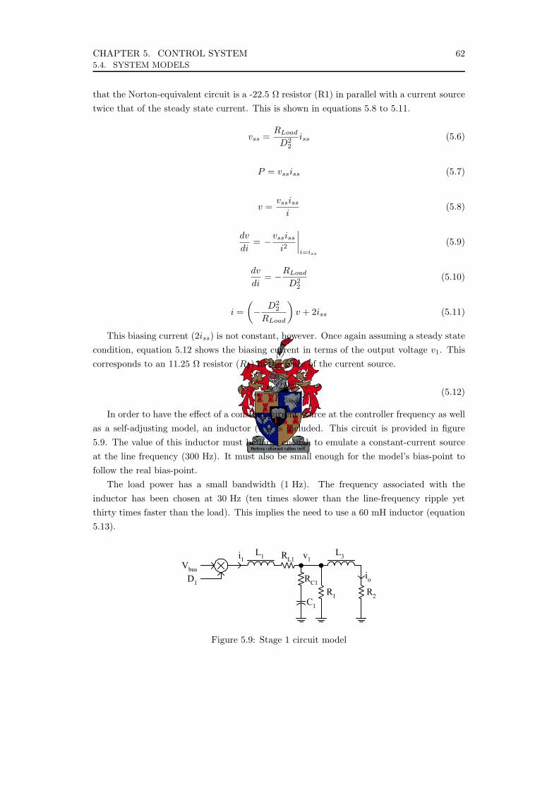
CHAPTER 5. CONTROL SYSTEM 625.4. SYSTEM MODELS
that the Norton-equivalent circuit is a -22.5 Ω resistor (R1) in parallel with a current sourcetwice that of the steady state current. This is shown in equations 5.8 to 5.11.
vss =RLoad
D22
iss (5.6)
P = vssiss (5.7)
v =vssiss
i(5.8)
dv
di= −vssiss
i2
∣∣∣∣i=iss
(5.9)
dv
di= −RLoad
D22
(5.10)
i =(− D2
2
RLoad
)v + 2iss (5.11)
This biasing current (2iss) is not constant, however. Once again assuming a steady statecondition, equation 5.12 shows the biasing current in terms of the output voltage v1. Thiscorresponds to an 11.25 Ω resistor (R2) in the place of the current source.
iss =2D2
2
RLoadv1 (5.12)
In order to have the effect of a constant current source at the controller frequency as wellas a self-adjusting model, an inductor (L3) is included. This circuit is provided in figure5.9. The value of this inductor must be large enough to emulate a constant-current sourceat the line frequency (300 Hz). It must also be small enough for the model’s bias-point tofollow the real bias-point.
The load power has a small bandwidth (1 Hz). The frequency associated with theinductor has been chosen at 30 Hz (ten times slower than the line-frequency ripple yetthirty times faster than the load). This implies the need to use a 60 mH inductor (equation5.13).
Chapter 5 – Control System : System Models 57
This biasing current (2iss) is not constant, however. Once again assuming a steady-state
condition, equation 5.9 shows the biasing current in terms of the output voltage v1. This corresponds to
an 11.25Ω resistor (R2) in the place of the current-source.
1
222 v
RDiLoad
ss = (5.9)
In order to have the effect of a constant current source at the controller frequency as well as a
self-adjusting model, an inductor (L3) is included. This circuit is provided in figure 5.11. The value of
this inductor must be large enough to emulate a constant-current source at the line frequency (300Hz).
It must also be small enough for the model’s bias-point to follow the real bias-point.
The load power has a small bandwidth (1Hz). The frequency associated with the inductor has
been chosen at 30Hz (ten times slower than the line-frequency ripple yet thirty times faster than the
load). This implies the need to use a 60mH inductor.
io
L3RL1
R2C1
R1
L1Vbus
D1
i1 v1
RC1
Figure 5.11 – Stage 1 circuit model
This model is valid only at the steady-state condition. It has been shown by simulation, however,
that the control system arising from this model performs well. Results of this simulation are provided
in section 5.5.
As full-state feedback and pole-placement techniques are used, a state-space model of this system
is required [6]. By using equations 5.10 to 5.12 [19], the model may be derived through algebraic
manipulation of the node-voltage equations [19]. The result is given by equations 5.13 through 5.15.
By allocating a vector x1, as in equation 5.16, the system model can be written in the form given by
equations 5.17 and 5.18, where ‘A1’, ‘B1’ and ‘C1’ are matrices given by equations 5.19 to 5.21.
iRv = (5.10)
dtdiLv = (5.11)
dtdvCi = (5.12)
Figure 5.9: Stage 1 circuit model

CHAPTER 5. CONTROL SYSTEM 635.4. SYSTEM MODELS
L =R
2πf(5.13)
This model is valid only at the steady state condition. It has been shown by simulation,however, that the control system arising from this model performs well. Results of thissimulation are provided in section 5.7. As full state feedback and pole-placement techniquesare used, a state-space model of this system is required [14]. By using equations 5.14 to5.16 [23], the model may be derived through algebraic manipulation of the node-voltageequations [23]. The result is given by equations 5.17 through 5.19. By allocating a vectorx1, as in equation 5.20, the system model can be written in the form given by equations5.21 and 5.22, where A1, B1 and C1 are matrices given by equations 5.23 to 5.25.
v = iR (5.14)
v = Ldi
dt(5.15)
i = Cdv
dt(5.16)
dv1
dt=
(−R1RC1L3C1−R1RC1L1C1−L1L3
L1L3C1(R1+RC1)
)v1+(
R1L1−R1RC1RL1C1L1C1(R1+RC1)
)i1+(
R1R2RC1C1−R1L3L3C1(R1+RC1)
)i0+(
R1RC1Vbus
L1(R1+RC1)
)D1
(5.17)
di1dt
=(− 1
L1
)v1 +
(−RL1
L1
)i1 + (0) i0 +
(Vbus
L1
)D1 (5.18)
di0dt
=(
1L3
)v1 + (0) i1 +
(−R2
L3
)i0 + (0)D1 (5.19)
x1 =
v1
i1
i0
(5.20)
x1 = A1x1 + B1D1Vbus (5.21)
v1 = C1x1 (5.22)
A1 =
−R1RC1L3C1−R1RC1L1C1−L1L3
L1L3C1(R1+RC1)R1L1−R1RC1RL1C1
L1C1(R1+RC1)R1R2RC1C1−R1L3
L3C1(R1+RC1)
− 1L1
−RL1L1
01
L30 −R2
L3
(5.23)
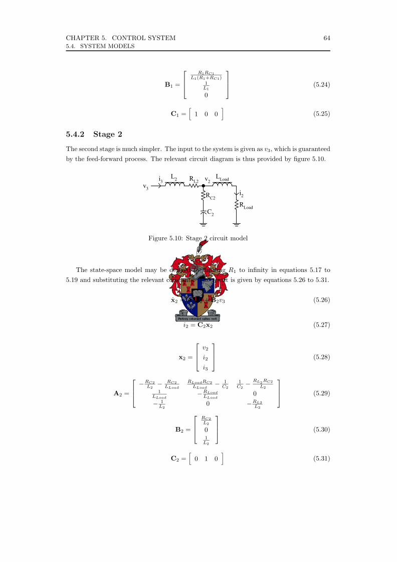
CHAPTER 5. CONTROL SYSTEM 645.4. SYSTEM MODELS
B1 =
R1RC1
L1(R1+RC1)1
L1
0
(5.24)
C1 =[
1 0 0]
(5.25)
5.4.2 Stage 2
The second stage is much simpler. The input to the system is given as v3, which is guaranteedby the feed-forward process. The relevant circuit diagram is thus provided by figure 5.10.
Chapter 5 – Control System : System Models 59
5.2.2 Stage 2 The second stage is much simpler. The input to the system is given as v3, which is guaranteed by
the feed-forward process. The relevant circuit diagram is thus provided by figure 5.12.
i2
LLoadRL2
RLoadC2
L2v3
i3 v2
RC2
Figure 5.12 – Stage 2 circuit model
The state-space model may be derived by limiting R1 to infinity in equations 5.13 and 5.15 and
substituting the relevant constants. The result is given by equations 5.22 to 5.27.
32222 vBxAx +=& (5.22)
222 xC=i (5.23)
=
3
2
2
2
iiv
x (5.24)
−−
−
−−−−
=
2
2
2
2
22
22
22
2
2
2
01
01
11
LR
L
LR
L
LRR
CCLRR
LR
LR
L
Load
Load
Load
CL
Load
CLoad
Load
CC
A (5.25)
=
2
2
2
210
L
LRC
B (5.26)
[ ]0102 =C (5.27)
Figure 5.10: Stage 2 circuit model
The state-space model may be derived by limiting R1 to infinity in equations 5.17 to5.19 and substituting the relevant constants. The result is given by equations 5.26 to 5.31.
x2 = A2x2 + B2v3 (5.26)
i2 = C2x2 (5.27)
x2 =
v2
i2
i3
(5.28)
A2 =
−RC2L2
− RC2LLoad
RLoadRC2LLoad
− 1C2
1C2
− RL2RC2
L21
LLoad−RLoad
LLoad0
− 1L2
0 −RL2L2
(5.29)
B2 =
RC2L2
01
L2
(5.30)
C2 =[
0 1 0]
(5.31)

CHAPTER 5. CONTROL SYSTEM 655.5. POLE PLACEMENT
5.4.3 Integrator
Figure 5.11 shows a closed loop system with an integrator for removing the steady stateerror.
Chapter 5 – Control System : Pole Placement 60
5.2.3 Integrator Figure 5.13 shows a closed loop system with an integrator for removing the steady-state error.
r ys
K inte u )(sH
Figure 5.13 – Integrator control
System H(s) is modelled as a state-space system implementing full-state feedback, as in equations
5.28 and 5.29. The state-space representation of the integrator is given by equation 5.30. The closed-
loop system can thus be modelled using equations 5.31 and 5.32.
[ ] NuBxBKAx ++=& (5.28)
Cx=y (5.29)
eKu int=& (5.30)
rKuK
Nu
+
−+
=
•
intint 00x
CBBKAx
(5.31)
[ ]
=
uy
xC 0 (5.32)
5.3 Pole Placement 5.3.1 Stage 1
The combination of L2 and R2 results in a zero at s = -R2/L3. In order for L3 and R2 to have no
effect, the first pole is placed exactly on this zero. Since the current through L3 is a fictional current
used only in simulation, the feedback gain associated with it is made zero. This moves the pole
slightly, but not enough to cause significant change in the ramp-response.
The maximum bandwidth of the closed-loop system is partly determined by the bandwidth of the
measurements (5kHz). Making the system bandwidth ten times lower than this (500Hz) causes the
system to become insensitive to measurement phase-error.
Also, the system must be able to follow the voltage reference fast enough so that the second stage
does not perceive the transient effect. As described earlier, a 1kV·s-1 ramp reference is the worst-case
scenario. Equation 5.33 shows the error (e) on a single-order system following a ramp-reference with
gradient ‘m’. It is derived in appendix B. A system that follows a 1kV·s-1 ramp with less than 1V error
must thus have a bandwidth of greater than 160Hz.
τme = (5.33)
Figure 5.11: Integrator control
System H(s) is modelled as a state-space system implementing full state feedback, asin equations 5.32 and 5.33. The state-space representation of the integrator is given byequation 5.34. The closed-loop system can thus be modelled using equations 5.35 and 5.36.
x = [A + BK]x + BNu (5.32)
y = Cx (5.33)
u = Kinte (5.34)
•[x
u
]=
[A + BK BN
−KintC 0
] [x
u
]+
[0
Kint
]r (5.35)
y =[
C 0] [
x
u
](5.36)
5.5 Pole Placement
5.5.1 Stage 1
The combination of L3 and R2 results in a zero at s = −R2/L3. In order for L3 and R2 tohave negligible effect, the first pole is placed as near as possible to this zero. Since the currentthrough L3 is a fictional current used only in simulation, the feedback gain associated withit is made zero. This moves the pole slightly, but not enough to cause significant change inthe step-response.
The maximum bandwidth of the closed-loop system is partly determined by thebandwidth of the measurements (5 kHz). Making the system bandwidth ten times lowerthan this ((500 Hz) causes the system to become insensitive to measurement phase-error.

CHAPTER 5. CONTROL SYSTEM 665.5. POLE PLACEMENT
The control law is given by equation 5.37. By writing the resulting state-spacerepresentation (equation 5.38), it is clear that a disturbance in bus voltage results in aslight movement of the poles and a shift in reference voltage. This in turn results in a shiftin steady state voltage, an effect that must be minimised. The steady state voltage is givenby equation 5.39. Conveniently, a smaller reference implies that bus voltage disturbanceshave a smaller effect.
D1 = K1x1 + N1vref (5.37)
x1 = [A1 + B1K1Vbus]x1 + B1N1vrefVbus (5.38)
v1,ss = C1 · [A1 + B1K1Vbus]−1 · [−B1N1vrefVbus] (5.39)
Various options for placing the poles are available. The first option is to use a 3rd
order Butterworth filter prototype [23]. This means that poles are placed as in equation5.40. Table 5-I shows the rejection obtained for a 75 V (peak to peak), 300 Hz sinusoidaldisturbance. The values provided are in relation to the output voltage. From this table itis clear that the higher the bandwidth, the better the rejection. As a result, the bandwidthof 500 Hz calculated above was retained.
s =
−ω
−ω±jω√
32
(5.40)
Table 5-I: Ripple rejection using a Butterworth prototype
Bandwidth Change in steady- Rejection due to Total rejection
[Hz] state voltage [dB] dynamics [dB] [dB]
100 2 16 14
200 -8 6 14
300 -15 2 17
400 -19 0 19
500 -23 0 23
600 -26 0 26
700 -29 0 29
800 -31 0 31
900 -33 0 33
1 000 -35 0 35
There is another option for pole-placement. This is to consider the often-used fast currentinner loop and slow voltage outer loop control, as described in section 5.3.2. This relates toplacing the one pole at 500 Hz and the other much further away from the origin. The faster

CHAPTER 5. CONTROL SYSTEM 675.5. POLE PLACEMENT
pole is then related to the current through the inductor. A higher bandwidth measurementis required. The LEM modules used to measure the current have a 0.5 dB bandwidth of100 kHz. A good cut-off frequency for the ADC filer is thus 100 kHz (1 nF capacitor in theplace of the 22 nF). Unfortunately the voltage measurement must be as noiseless as possiblefor feed-forward purposes and thus the 5 kHz bandwidth is retained for v1. Table 5-II showsthe effect of placing the slow pole at 500 Hz and the faster one at other frequencies. Thesame 75 Vp-p, 300 Hz disturbance is used.
Table 5-II: Ripple rejection using faster current feedback
Fast pole Change in steady- Rejection due to Total rejection
placement [Hz] state voltage [dB] dynamics [dB] [dB]
500 -23 2 25
700 -26 1 27
1 000 -29 1 30
1 400 -32 1 33
2 000 -35 1 36
2 600 -37 1 38
3 700 -40 1 41
5 000 -43 1 44
7 000 -46 1 47
10 000 -49 1 50
By using this technique and placing both poles ten times slower than their respectivemeasurement filters a, 50 dB rejection is possible. This is an improvement on the 23 dBachieved when using a Butterworth prototype.
As a final consideration, the switching frequency is 47.684 kHz. 10 kHz is 5 times slowerthan this, an acceptable condition, although 10 times slower would be advised. The polesare thus placed at 500 Hz and 5 kHz.
The desired characteristic equation for arbitrary pole placement is given by equation5.41. The order of the system is given by n. By using Ackermann’s formula [14] (describedby equations 5.42 to 5.44) the poles can be placed directly. Matrix C is the controllabilitymatrix – for the system to be controllable, this matrix has to be invertible. The α termsin these equations represent the coefficients of the characteristic equation of the desiredclosed-loop system.
αc(s) = sn + α1sn−1 + α2s
n−2 + · · ·+ αn = 0 (5.41)
αc(A) = An + α1An−1 + α2An−2 + · · ·+ αnI (5.42)
C =[
B AB A2B · · · An−1B]
(5.43)
CHAPTER 5. CONTROL SYSTEM 685.5. POLE PLACEMENT
K =[
0 · · · 0 1]C−1αc(A) (5.44)
After implementation of such a full state feedback controller, the system will be stable.It is guaranteed stable because the position of the closed-loop poles have been placed on theleft-hand side of the complex plane.
The steady state of the output is not guaranteed to equal the reference. This steadystate error requires removal. Equations 5.45 and 5.46 describe how to calculate the referencegain (N) that will result in a total removal of this error. These equations are repeated from[14]. The calculated gains are listed in table 5-III.[
Nx
Nu
]=
[A B
C 0
]−1 [0
1
](5.45)
N = Nu −KNx (5.46)
Table 5-III: Stage 1 gains
Gain Value
V1 -0.2666
I1 -0.1915
N1 0.2769
5.5.2 Stage 2
The second stage essentially consists of three parts. First the control system designed bypole-placement (H(s)). Second the steady state error is removed by means of scaling thereference. Third the integrator is designed, where the gain must be determined by alternativemethods.
By placing the poles of H(s) using a Butterworth prototype ten times faster than theclosed-loop bandwidth (10 Hz), the calculation of the integrator gain is straightforward.This also enables the closed-loop system to have a single-order response, with the advantageof no overshoot.
By inserting a pole at the origin (representing the integrator) and drawing the root-locus, the effect of the integrator gain may be noted. The two real poles move towards eachother at an equal rate. The two complex poles do the same, but to a lesser extent. This isshown in figure 5.12. The crosses represent the original poles and the squares the resultingclosed-loop poles.
The poles for H(s) are thus placed using an 11 Hz Butterworth prototype. These polesare listed in equation 5.47. In the closed-loop system, the real pole is moved to 10 Hz and
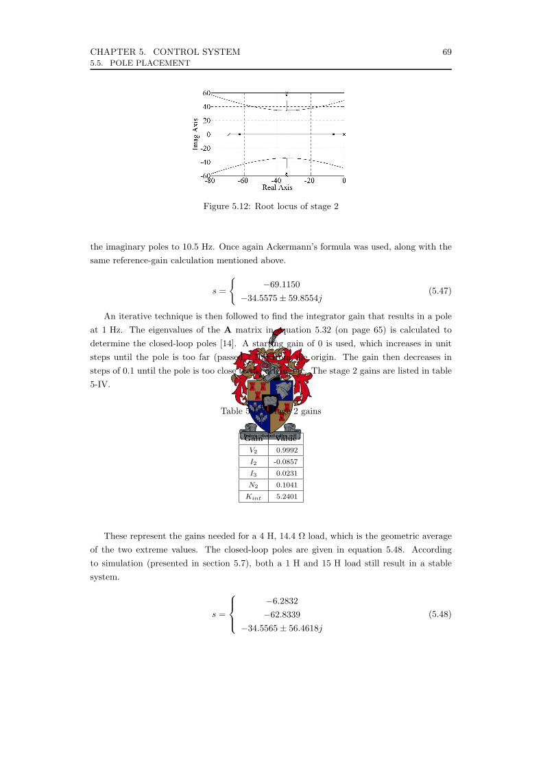
CHAPTER 5. CONTROL SYSTEM 695.5. POLE PLACEMENT
Figure 5.12: Root locus of stage 2
the imaginary poles to 10.5 Hz. Once again Ackermann’s formula was used, along with thesame reference-gain calculation mentioned above.
s =
−69.1150
−34.5575± 59.8554j(5.47)
An iterative technique is then followed to find the integrator gain that results in a poleat 1 Hz. The eigenvalues of the A matrix in equation 5.32 (on page 65) is calculated todetermine the closed-loop poles [14]. A starting gain of 0 is used, which increases in unitsteps until the pole is too far (passed 1 Hz) from the origin. The gain then decreases insteps of 0.1 until the pole is too close to the origin, etc. The stage 2 gains are listed in table5-IV.
Table 5-IV: Stage 2 gains
Gain Value
V2 0.9992
I2 -0.0857
I3 0.0231
N2 0.1041
Kint 5.2401
These represent the gains needed for a 4 H, 14.4 Ω load, which is the geometric averageof the two extreme values. The closed-loop poles are given in equation 5.48. Accordingto simulation (presented in section 5.7), both a 1 H and 15 H load still result in a stablesystem.
s =
−6.2832−62.8339
−34.5565± 56.4618j
(5.48)
CHAPTER 5. CONTROL SYSTEM 705.6. MEASUREMENTS
5.6 Measurements
5.6.1 Analogue vs Digital
There are obvious advantages to use a digital control system for stage 2. These include theease of feed-forward implementation, adaptability of the control system, etc.
There are many analogue control ICs available on the market for an isolated full-bridgetopology. They implement many high-performance control techniques and are inexpensive.It is possible to provide one of these ICs with a reference signal from a 12-bit DAC, resultingin the correct output voltage needed for the input to stage 2.
This 12-bit DAC costs about the same as the 12-bit ADC needed to measure i1, solvingthe cost issue. Also, a high-precision measurement of v1 is taken for feed-forward purposes,which can be used for the stage 1 control system. The FPGA is already present, and socan be used to control the first stage as well as the second stage. A digital control systemalso offers ease of adjustment to different control specifications. The entire control systemis thus implemented digitally.
This choice of digital control also has other implications. There is no possibility of peakcurrent control, for instance. This is because the ADCs sample too slowly. Faster ADCshave lower resolution, which is not acceptable in this high-precision application.
5.6.2 Resolution
The resolution of the measurements is mainly dictated by the available technology. Thehighest resolution, >400 ksps, single-sample latency ADC that was found is the AD7674from Analog Devices. It samples at 800 ksps with a resolution of 18-bit. This is coincidentlya convenient resolution, since the FPGA has on-board 18-bit multipliers.
Upon closer inspection, a resolution of 18-bit does not seem precise enough. Use v1
as an example: it has a full-scale value of 400 V, with a resolution of 1.526 mV. This issatisfactory for the control of stage 1, but not for the feed-forward of stage 2. At minimum-load, the first stage output voltage is 18 V and 10 ppm of that is 180 µV – 8.5 times smallerthan the available resolution. An extra 4 bits resolution is thus required for proper control.
There is a random component to the signal due to Gaussian noise, switching transientsand switching ripple. If the past 16 samples are averaged, a 22-bit signal is obtained. These16 samples correspond exactly to one switching cycle of stage 1 – i.e. all four switchingstates. The result will thus always be approximately that of the cycle-average. The standarddeviation of the noise is reduced by a factor four (
√16) [28].
In [11] output current measurement noise is reduced by taking the measurement at threedifferent points on the circuit and using two different techniques. These measurements arethen averaged. This is shown in figure 5.13.
Another technique that may be used to improve analogue to digital conversion is to utilisetwo separate ADCs of different specifications – one with high-resolution, but a low samplerate and the other with a high sample rate, but low-resolution. The inputs to the fast- andslow ADCs pass through complementary high- and low-pass filters respectively. When the

CHAPTER 5. CONTROL SYSTEM 715.6. MEASUREMENTS
Chapter 1 – Control System : Measurements 16
factor four (√16).
In [1] output current measurement noise is reduced by taking the measurement at three different
points on the circuit and using two different techniques. These measurements are then averaged. This
is shown in figure 5.15.
22-bitADC
OutputVoltage
Controller
Reference
Current measurement2
Load inductance
Load resistance
Current sence resistorCurrent measurement3
Current measurement1
Figure 1.15 – Multiple measurements
Another technique that may be used to improve analogue to digital conversion is to utilise two
separate ADCs of different specifications – one with high-resolution, but a low sample-rate and the
other with a high sample-rate, but low-resolution. The inputs to the fast- and slow ADCs pass through
complimentary high- and low-pass filters respectively. When the two measurements are then added, a
high sample-rate is obtained at high frequencies and a high resolution at low frequencies. This
technique works well when the closed-loop system is required to have a fast settling-time, but is not
needed to follow a high-bandwidth signal with great accuracy.
This project requires that the line-frequency ripple on v1 be removed accurately, and therefore
requires the high-frequency measurement to have as small as possible latency. Very high resolution
ADCs have large latencies and therefore would not be the correct choice for use in this project.
1.4.3 Actual Measurements High-resolution ADCs are expensive and careful consideration must be taken as to which
measurements are necessary. The mathematical models of the circuit are well known and it is therefore
possible to take as few measurements as possible. In order for protection circuitry to function properly,
however, more measurements are required.
There are two high-precision measurements which are absolutely necessary. These are the output
current i2 (for using current feedback when the NMR measurement is unavailable) and the feed-forward
voltage v1.
Figure 5.13: Multiple measurements
two measurements are then added, a high sample rate is obtained at high frequencies and ahigh resolution at low frequencies. This technique works well when the closed-loop systemis required to have a fast settling time, but is not needed to follow a high-bandwidth signalwith great accuracy.
This project requires that the line-frequency ripple on v1 be removed accurately, andtherefore requires the high-frequency measurement to have as small as possible latency.Very high resolution ADCs have large latencies and therefore would not be the correctchoice for use in this project.
A third option exists. A multiplying DAC (such as the DAC7800 from TexasInstruments) can be used to scale the input signal. A small input signal can then be scaled1:1, whereas larger signals can be scaled 2:1, 4:1, etc. This means that the sampled signalhas better resolution for smaller signals, which would then satisfy the 10 ppm requirement.
5.6.3 Actual Measurements
High-resolution ADCs are expensive and careful consideration must be taken as to whichmeasurements are necessary. The mathematical models of the circuit are well known andit is therefore possible to take as few measurements as possible. In order for protectioncircuitry to function properly, however, more measurements are required.
There are two high-precision measurements which are absolutely necessary. These are theoutput current i2 (for using current feedback when the NMR measurement is unavailable)and the feed-forward voltage v1.
There are also two less important measurements necessary. These are the output voltagev2 (for determining the load characteristics) and the stage 1 inductor current i1 (for controland protection purposes). These may be calculated using the mathematical model of thecircuit (described in the following section) and therefore do not need to have high precision.
Since the ADCs were obtained on sample, however, the same AD7674 ADCs were used.It is also convenient for prototyping purposes, since a lower resolution ADC can very easilybe simulated using measurements from one with a high resolution, but not vice versa.
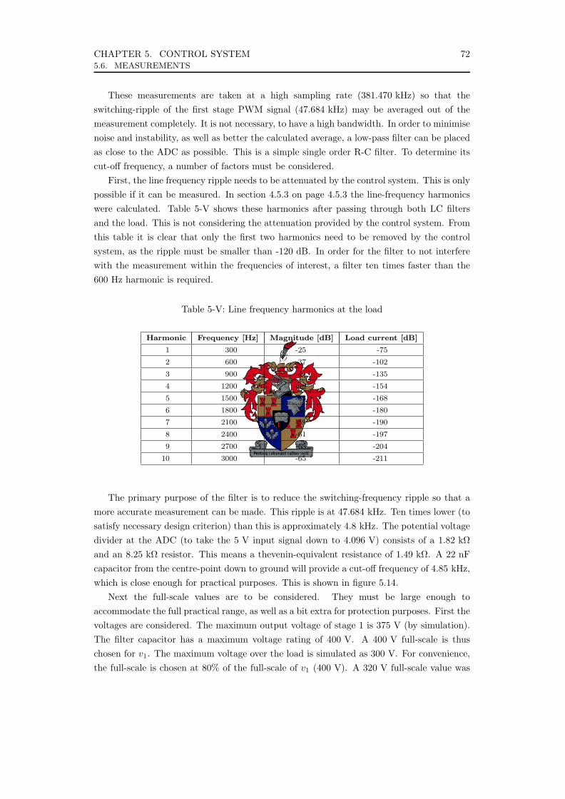
CHAPTER 5. CONTROL SYSTEM 725.6. MEASUREMENTS
These measurements are taken at a high sampling rate (381.470 kHz) so that theswitching-ripple of the first stage PWM signal (47.684 kHz) may be averaged out of themeasurement completely. It is not necessary, to have a high bandwidth. In order to minimisenoise and instability, as well as better the calculated average, a low-pass filter can be placedas close to the ADC as possible. This is a simple single order R-C filter. To determine itscut-off frequency, a number of factors must be considered.
First, the line frequency ripple needs to be attenuated by the control system. This is onlypossible if it can be measured. In section 4.5.3 on page 4.5.3 the line-frequency harmonicswere calculated. Table 5-V shows these harmonics after passing through both LC filtersand the load. This is not considering the attenuation provided by the control system. Fromthis table it is clear that only the first two harmonics need to be removed by the controlsystem, as the ripple must be smaller than -120 dB. In order for the filter to not interferewith the measurement within the frequencies of interest, a filter ten times faster than the600 Hz harmonic is required.
Table 5-V: Line frequency harmonics at the load
Harmonic Frequency [Hz] Magnitude [dB] Load current [dB]
1 300 -25 -75
2 600 -37 -102
3 900 -44 -135
4 1200 -49 -154
5 1500 -53 -168
6 1800 -56 -180
7 2100 -59 -190
8 2400 -61 -197
9 2700 -63 -204
10 3000 -65 -211
The primary purpose of the filter is to reduce the switching-frequency ripple so that amore accurate measurement can be made. This ripple is at 47.684 kHz. Ten times lower (tosatisfy necessary design criterion) than this is approximately 4.8 kHz. The potential voltagedivider at the ADC (to take the 5 V input signal down to 4.096 V) consists of a 1.82 kΩand an 8.25 kΩ resistor. This means a thevenin-equivalent resistance of 1.49 kΩ. A 22 nFcapacitor from the centre-point down to ground will provide a cut-off frequency of 4.85 kHz,which is close enough for practical purposes. This is shown in figure 5.14.
Next the full-scale values are to be considered. They must be large enough toaccommodate the full practical range, as well as a bit extra for protection purposes. First thevoltages are considered. The maximum output voltage of stage 1 is 375 V (by simulation).The filter capacitor has a maximum voltage rating of 400 V. A 400 V full-scale is thuschosen for v1. The maximum voltage over the load is simulated as 300 V. For convenience,the full-scale is chosen at 80% of the full-scale of v1 (400 V). A 320 V full-scale value was

CHAPTER 5. CONTROL SYSTEM 735.6. MEASUREMENTS
Chapter 5 – Control System : Measurements 68
The primary purpose of the filter is to remove the switching-frequency ripple to some extent.
This ripple is at 47.684kHz. Ten times lower (to satisfy necessary design criterion) than this is
approximately 4.8kHz. The potential voltage divider at the ADC (to take the 5V input signal down to
4.096V) consists of a 1.82kΩ and an 8.25kΩ resistor. This means a thevenin-equivalent resistance of
1.49kΩ. A 22nF capacitor from the centre-point down to ground will provide a cut-off frequency of
4.85kHz, which is near enough for practical purposes. This is shown in figure 5.16.
5V Input1.82kΩ
8.25kΩ 22nF
To ADC
Figure 5.16 – ADC pre-filter circuit diagram
Next the full-scale values are to be considered. They must be large enough to accommodate the
full practical range, as well as a bit extra for protection purposes. First the voltages are considered.
The maximum output voltage of stage 1 is 375V (by simulation). The filter capacitor has a maximum
voltage rating of 400V. A 400V full-scale is thus chosen for v1. The maximum voltage over the load is
simulated as 300V. For convenience, the full-scale is chosen at 80% of the full-scale of v1 (400V). A
320V full-scale value was thus chosen. The maximum currents through the stage 1 filter inductor (i1)
and load (i2) are 12A and 15A respectively. Full-scale values of 15A and 20A were thus chosen.
The exact time at which to take the measurements is also an important issue. It is required that
switching transients do not affect the measurement. The only time that the transistors are guaranteed to
not switch is just before the rising-edge of the PWM signal. The AD7674 has an aperture delay of 2ns
(0.08% of the 2.62144µs sampling period). The maximum duty-cycle of the second stage PWM signal
is 95% (2.49µs). The time delay for the MOSFET to switch on or off is in the order of 200ns. Taking
the measurement at the same time as the PWM signal’s rising-edge is thus optimal.
5.4.4 Estimated The only measurement that is not taken directly is the current through the filter inductor of stage 2
(i3). It can be calculated, however, by using equation 5.44.
22
23 idt
dvCi += (5.44)
Figure 5.14: ADC pre-filter circuit diagram
thus chosen. The maximum currents through the stage 1 filter inductor (i1) and load (i2)are 12 A and 15 A respectively. Full-scale values of 15 A and 20 A were thus chosen.
The exact time at which to take the measurements is also an important issue. It isrequired that switching transients do not affect the measurement. The only time that thetransistors are guaranteed to not switch is just before the rising-edge of the PWM signal.The AD7674 has an aperture delay of 2 ns (0.08% of the 2.621 44 µs sampling period). Themaximum duty-cycle of the second stage PWM signal is 95% (2.49 µs). The time delay forthe MOSFET to switch on or off is in the order of 200 ns. Taking the measurement at thesame time as the PWM signal’s rising-edge is thus optimal.
5.6.4 Estimated
The only measurement that is not taken directly is the current through the filter inductorof stage 2 (i3). It can be calculated, however, by using equation 5.49.
i3 = C2dv2
dt+ i2 (5.49)
As mentioned in the previous section, i1 and v2 can be calculated using the propertiesof the system. These are presented by equations 5.50 and 5.51.
i1 = C1dv1
dt+ i3D2 (5.50)
v2 = LLoaddi2dt
+ RLoadi2 (5.51)
The load characteristics needed to calculate v2 can be calibrated by the system. It isthus possible to have v1 and i2 as the only measurements. For the prototype, however, i3 isthe only estimated value – the rest are measured.
5.6.5 Noise
Any high-resolution measurement contains noise. In the case of this project, switching noiseis minimised by taking the measurement just before the rising switching edge. The noiseto be considered is thus thermal Gaussian noise and switching ripple. Using a 5 kHz filterbefore each ADC minimises the noise power and so also the measurement error.
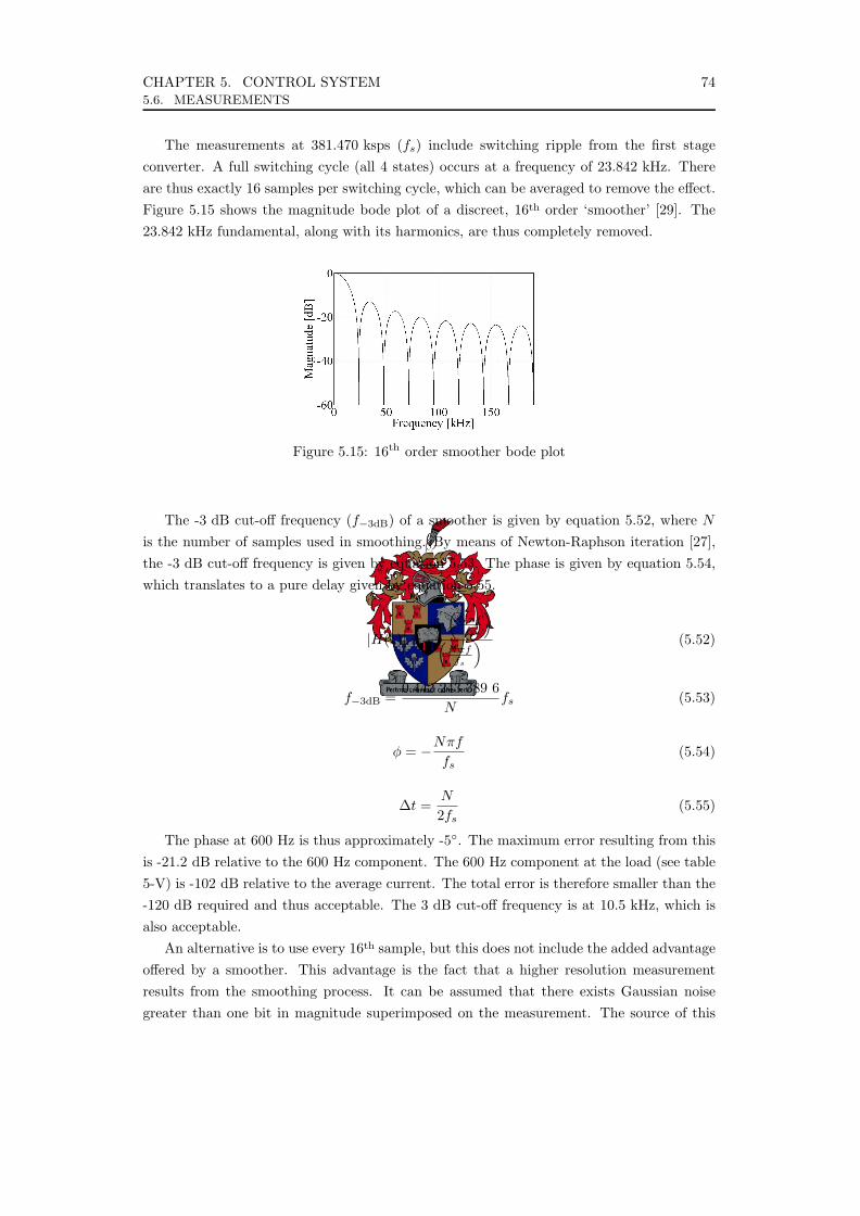
CHAPTER 5. CONTROL SYSTEM 745.6. MEASUREMENTS
The measurements at 381.470 ksps (fs) include switching ripple from the first stageconverter. A full switching cycle (all 4 states) occurs at a frequency of 23.842 kHz. Thereare thus exactly 16 samples per switching cycle, which can be averaged to remove the effect.Figure 5.15 shows the magnitude bode plot of a discreet, 16th order ‘smoother’ [29]. The23.842 kHz fundamental, along with its harmonics, are thus completely removed.
Figure 5.15: 16th order smoother bode plot
The -3 dB cut-off frequency (f−3dB) of a smoother is given by equation 5.52, where N
is the number of samples used in smoothing. By means of Newton-Raphson iteration [27],the -3 dB cut-off frequency is given by equation 5.53. The phase is given by equation 5.54,which translates to a pure delay given by equation 5.55.
|H(z)| =sin
(Nπffs
)(
Nπffs
) (5.52)
f−3dB =0.442 243 389 6
Nfs (5.53)
φ = −Nπf
fs(5.54)
∆t =N
2fs(5.55)
The phase at 600 Hz is thus approximately -5. The maximum error resulting from thisis -21.2 dB relative to the 600 Hz component. The 600 Hz component at the load (see table5-V) is -102 dB relative to the average current. The total error is therefore smaller than the-120 dB required and thus acceptable. The 3 dB cut-off frequency is at 10.5 kHz, which isalso acceptable.
An alternative is to use every 16th sample, but this does not include the added advantageoffered by a smoother. This advantage is the fact that a higher resolution measurementresults from the smoothing process. It can be assumed that there exists Gaussian noisegreater than one bit in magnitude superimposed on the measurement. The source of this

CHAPTER 5. CONTROL SYSTEM 755.7. SIMULATION
noise is partly thermal and partly quantisation effects. The standard deviation of the averageof 16 random samples taken from a Gaussian distribution is one quarter of the standarddeviation of that distribution. That implies that an extra 2 bits of resolution are obtained.
Similarly, by using a 256-sample smoother (using one M4K memory block in the cycloneII FPGA) another 4 bits are gained. An M4K block is a block of embedded memory4 096 bits large. With this type of smoother, the output current i2 can be measured witha resolution of 22-bit. The bandwidth of the measurement drops to 659 Hz, which is stillmuch higher than the 1 Hz bandwidth of the controller.
5.6.6 Other
With an ultra-stable clock (<1 ppm·C-1) frequency can be measured to better than 10 ppm(provided the temperature remains within 10 C of the average). The remaining error isremoved by calibration. This accuracy is not practically possible when measuring current orvoltage, however. It is thus imperative to provide the control system with the field-strength,which is dependant on a frequency measurement when using NMR techniques.
5.7 Simulation
5.7.1 Stage 1
MATLAB simulations were run to validate the designed control system using a simpleforward Euler integration technique [27]. The circuit in figure 5.9 was implemented. Table5-VI lists the circuit parameters. Figure 5.16 shows the response of the system to a rampedreference of 1 kV·s-1 from 0 to 375 V.
Table 5-VI: Stage 1 simulation circuit parameters
Parameter Value
Vbus 535 V
L1 3 mH
RL1 50 mΩ
C1 470 µF
RC1 10 mΩ
R1 -22.5 Ω
L3 60 mH
R2 11.25 Ω
The voltage reference is followed with negligible error, even at the transient point at 0 msand 375 ms. The current waveform shows small transients at these points, but of negligiblemagnitude.

CHAPTER 5. CONTROL SYSTEM 765.7. SIMULATION
(a) Stage 1 output voltage (b) Stage 1 output current
Figure 5.16: Stage 1 ramp response
Figure 5.17 shows the response of the system to a constant 270 V reference, but withthe bus voltage stepped from 560 V to 485 V and back.
(a) Stage 1 output voltage (b) Stage 1 output current
Figure 5.17: Stage 1 step disturbance
As predicted by equation 5.39 on page 66, the step disturbance causes a output voltagedisturbance similar in shape as the system step-response. The output current disturbanceis derivative of the voltage waveform around the 12 A bias point. A rejection ratio of47.64 dB is obtained
5.7.2 Stage 2
MATLAB was also used to simulate the second stage. The system is simulated using thesame control gains, but with different load inductances. The control gains are calculated fora 4 H load inductor, as mentioned in section 5.5.2. The rest of the circuit parameters arelisted in table 5-VII.
Figure 5.18a shows the step response of H(s) (see figure 5.11), which is the closed-loopsystem without the integrator loop. Figure 5.18b shows the closed-loop system including

CHAPTER 5. CONTROL SYSTEM 775.7. SIMULATION
Table 5-VII: Stage 1 simulation circuit parameters
Parameter Value
L2 200 µH
RL2 50 mΩ
C2 470 µF
RC2 10 mΩ
RLoad 14.4 Ω
the integrator loop. The results are exactly as expected – a fast, critically damped systemwithout the integrator and a single-order response with the integrator loop present.
(a) Pure H(s) (b) With integrator loop
Figure 5.18: Stage 2 simulation: 4 H
As designed in section 5.5.2, the pure H(s) step response shown in figure 5.18a is a 3rd
order Butterworth response with a bandwidth of 11 Hz. When the integrator is included,the response changes to the single order step response with a bandwidth of 1 Hz seen infigure 5.18b.
Figure 5.19 shows the result of a 1 to 15 A ramp-limited step response of the completesystem. The response of a 15 A to 1 A ramp-limited step is also included on the samegraphs.
Figures 5.20 and 5.21 show the results from repeating the above simulation with a 15 Hload inductor. Due to the larger inductance, the pure H(s) response is slower, as can beseen in figure 5.20a. It is interesting to note that the closed loop system with the integratorincluded still settles within 1 s.
The voltage overshoot required to charge the load is much larger, as can be seen in figure5.21a, but the resulting output current response remains the same.
Figures 5.22 and 5.23 show the results from using a 1 H load inductor. The resultingresponse is under damped, as can be seen in figure 5.22a. The reason for this is that theload responds quicker to an output voltage change than the control system anticipates. The
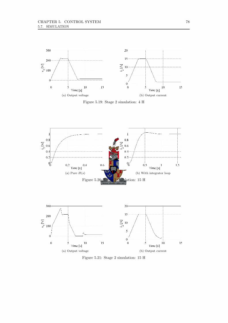
CHAPTER 5. CONTROL SYSTEM 785.7. SIMULATION
(a) Output voltage (b) Output current
Figure 5.19: Stage 2 simulation: 4 H
(a) Pure H(s) (b) With integrator loop
Figure 5.20: Stage 2 simulation: 15 H
(a) Output voltage (b) Output current
Figure 5.21: Stage 2 simulation: 15 H
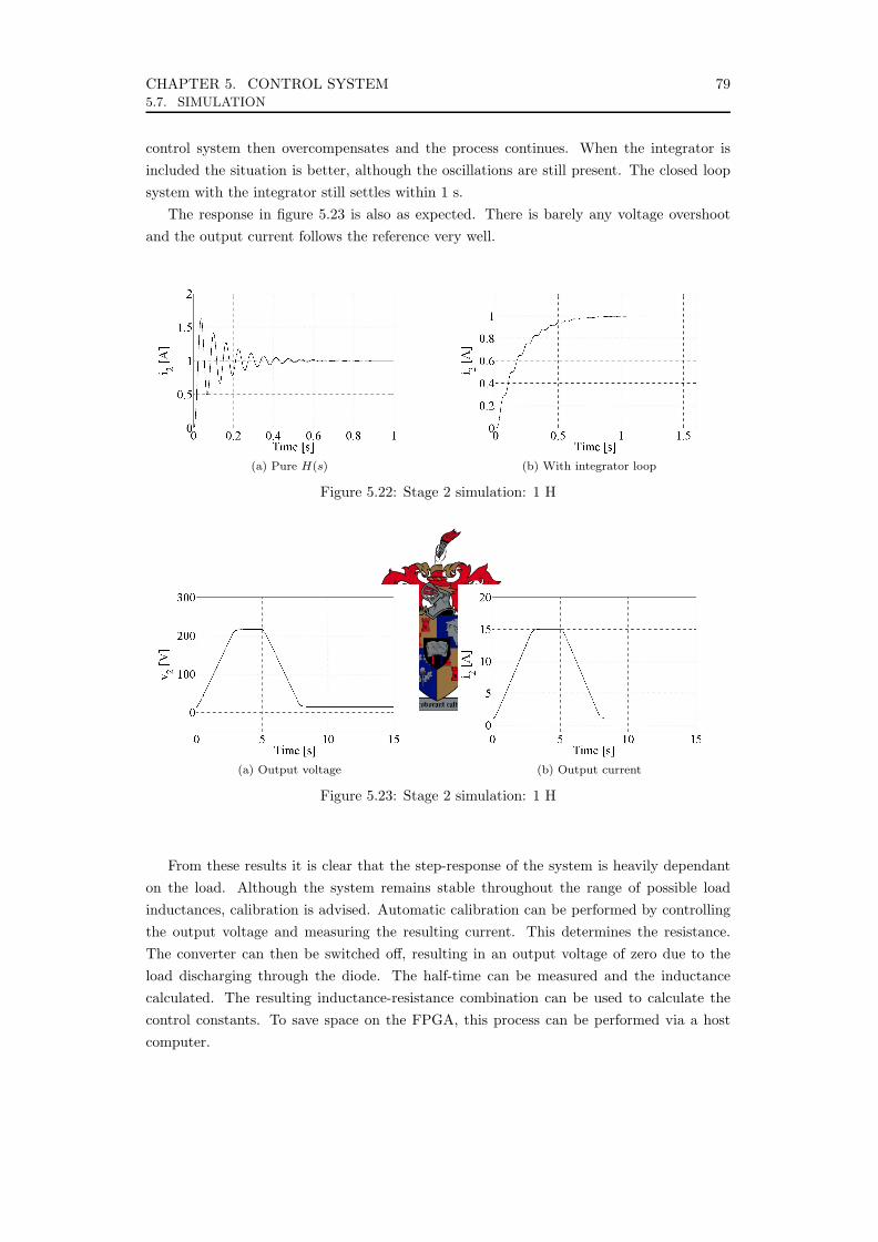
CHAPTER 5. CONTROL SYSTEM 795.7. SIMULATION
control system then overcompensates and the process continues. When the integrator isincluded the situation is better, although the oscillations are still present. The closed loopsystem with the integrator still settles within 1 s.
The response in figure 5.23 is also as expected. There is barely any voltage overshootand the output current follows the reference very well.
(a) Pure H(s) (b) With integrator loop
Figure 5.22: Stage 2 simulation: 1 H
(a) Output voltage (b) Output current
Figure 5.23: Stage 2 simulation: 1 H
From these results it is clear that the step-response of the system is heavily dependanton the load. Although the system remains stable throughout the range of possible loadinductances, calibration is advised. Automatic calibration can be performed by controllingthe output voltage and measuring the resulting current. This determines the resistance.The converter can then be switched off, resulting in an output voltage of zero due to theload discharging through the diode. The half-time can be measured and the inductancecalculated. The resulting inductance-resistance combination can be used to calculate thecontrol constants. To save space on the FPGA, this process can be performed via a hostcomputer.
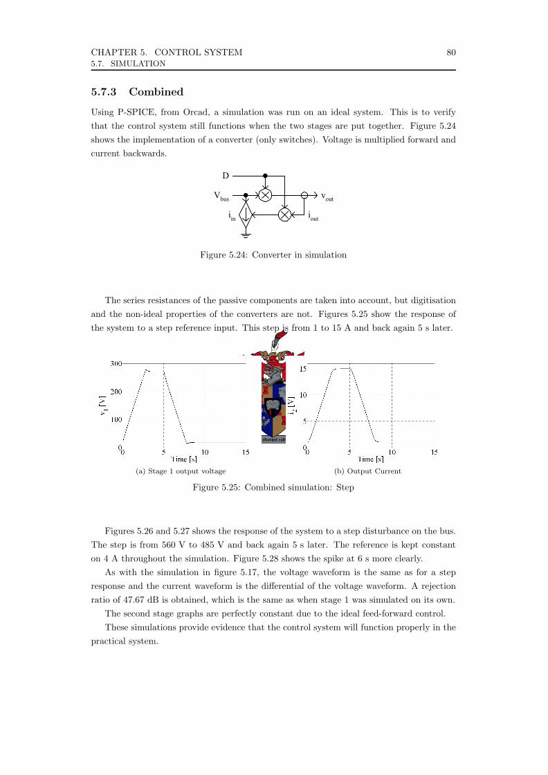
CHAPTER 5. CONTROL SYSTEM 805.7. SIMULATION
5.7.3 Combined
Using P-SPICE, from Orcad, a simulation was run on an ideal system. This is to verifythat the control system still functions when the two stages are put together. Figure 5.24shows the implementation of a converter (only switches). Voltage is multiplied forward andcurrent backwards.
Chapter 5 – Control System : Simulation 74
Figure 5.25 – Stage 2 simulation: 1H
From these results it is clear that the step-response of the system is heavily dependant on the load.
The step response after the ramp-limiter is inserted, however is much less sensitive to the load. No
calibration is necessary.
5.5.3 Combined Using P-SPICE, from Orcad, a simulation was run on an ideal system. This is to verify that the
control system still functions when the two stages are put together. Figure 5.26 shows the
implementation of a converter (only switches). Voltage is multiplied forward and current backwards.
Vbus vout
D
ioutiin
Figure 5.26 – Converter in simulation
The series resistances of the passive components are taken into account, but digitisation and the
non-ideal properties of the converters are not. Figures 5.27 show the response of the system to a step
reference input. This step is from 1 to 15 A and back again 5s later.
Figure 5.27 – Combined simulation: Step
Figure 5.24: Converter in simulation
The series resistances of the passive components are taken into account, but digitisationand the non-ideal properties of the converters are not. Figures 5.25 show the response ofthe system to a step reference input. This step is from 1 to 15 A and back again 5 s later.
(a) Stage 1 output voltage (b) Output Current
Figure 5.25: Combined simulation: Step
Figures 5.26 and 5.27 shows the response of the system to a step disturbance on the bus.The step is from 560 V to 485 V and back again 5 s later. The reference is kept constanton 4 A throughout the simulation. Figure 5.28 shows the spike at 6 s more clearly.
As with the simulation in figure 5.17, the voltage waveform is the same as for a stepresponse and the current waveform is the differential of the voltage waveform. A rejectionratio of 47.67 dB is obtained, which is the same as when stage 1 was simulated on its own.
The second stage graphs are perfectly constant due to the ideal feed-forward control.These simulations provide evidence that the control system will function properly in the
practical system.
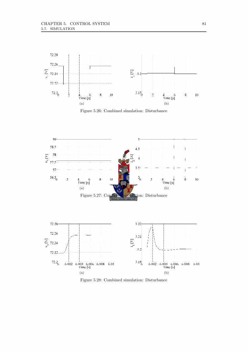
CHAPTER 5. CONTROL SYSTEM 815.7. SIMULATION
(a) (b)
Figure 5.26: Combined simulation: Disturbance
(a) (b)
Figure 5.27: Combined simulation: Disturbance
(a) (b)
Figure 5.28: Combined simulation: Disturbance
CHAPTER 5. CONTROL SYSTEM 825.8. SOFT-START
5.8 Soft-Start
5.8.1 Rectifier
Rectified 400 V 3-phase is never smaller than 490 V. For this reason, and considering therelatively large bus-capacitor, the system cannot simply be switched on without causingdamage. The capacitor must be charged slowly before it can be connected directly to themains. This can be done in many ways.
Three triacs are used to switch the mains on and off. It is possible to detect the zero-crossing between two of the three phases and switch them on at that point. The third isswitched on later to complete the circuit. It is easy to show that the inrush current (ignoringline-inductance) is given by equation 5.56 where C is the capacitance of the bus-capacitor,VL−L the peak line to line voltage and f the line-frequency (50 Hz). Problems with thiscircuit include the necessity to detect the zero-crossing as well as a very large peak inrushcurrent.
i =
CVL−L(2πfL) · cos(2πfLt) , t < 1
4fL
0 , otherwise(5.56)
A more attractive technique is to charge the capacitor through a resistor (R). This resistorhas a switch in parallel with it, which closes after the bus is fully charged. A relay may beused for this purpose, as can a MOSFET. The MOSFET has no moving parts, making itthe more attractive option as far as robustness and lifetime is concerned. A relay, however,does have near-zero losses and would be the preferred option for high-power converters. It isalso possible to use a thyristor, but a MOSFET or relay is more controllable. The chargingcurrent and voltage are given by equations 5.57 and 5.58 respectively.
i =VL−L
Re−t/RC (5.57)
v = VL−L
(1− e−t/RC
)(5.58)
This resistor-switch combination can be inserted either above or below the bus capacitor.It is advisable, however, to use the most negative node as a stable reference voltage. It isthus better to put this charging circuit above the bus-capacitor. This circuit is presented infigure 5.29.
First, a ‘power-good’ signal is received from the control board (which receives it directlyfrom the ATX power supply). This signal triggers the triacs to switch on, after which thebus capacitors charge through the resistor. A timer is used to close the switch, connectedin parallel to this resistor, after the capacitors are fully charged (after 3 s). When the‘power-good’ signal is low, the triacs are switched off.

CHAPTER 5. CONTROL SYSTEM 835.9. FIRMWARE IMPLEMENTATION
Chapter 4 – Converter : Soft-Start 30
Three triacs are used to switch the mains on and off. It is possible to detect the zero-crossing
between two of the three phases and switch them on at that point. The third is switched on later to
complete the circuit. It is easy to show that the inrush current (ignoring line-inductance) is given by
equation 4.4 where ‘C’ is the capacitance of the bus-capacitor, ‘VL-L’ the peak line to line voltage and
‘f’ the line-frequency (50Hz). Problems with this circuit include the necessity to detect the zero-
crossing as well as a very large peak inrush current.
<⋅
= −
otherwisef
ttffCViL
LLLL
,041,)2cos()2( ππ (4.4)
A more attractive technique is to charge the capacitor through a resistor (R). This resistor has a
switch in parallel with it, which closes after the bus is fully charged. A relay may be used for this
purpose, as can a MOSFET. The MOSFET has no moving parts, making it the more attractive option
as far as robustness and lifetime is concerned. A relay, however, does have near-zero losses and would
be the preferred option for high-power converters. It is also possible to use a thyristor, but a MOSFET
or relay is more controllable. The charging current and voltage are given by equations 4.5 and 4.6
respectively.
RCt
LL eR
Vi−
−= (4.5)
)1( RCt
LL eVv−
− −= (4.6)
This resistor-switch combination can be inserted either above or below the bus capacitor. It is
advisable, however, to use the most negative node as a stable reference voltage. It is thus better to put
this charging circuit above the bus-capacitor. This circuit is presented in figure 4.6.
Fuse3-phase in
Delay(2s)
Charge-pumpPower Good
To bus capacitors
500Ω
Figure 4.6 – Bus charging circuit
First, a ‘power-good’ signal is received from the control board (which receives it directly from
the ATX power-supply). This signal triggers the triacs to switch on, after which the bus capacitors
charge through the resistor. A timer is used to close the switch, connected in parallel to this resistor,
after the capacitors are fully charged. When the ‘power-good’ signal is low, the triacs are switched off.
Figure 5.29: Bus charging circuit
5.8.2 Converter
Both the output filters and the transformer need to be started slowly. At start-up, the outputfilter of stage 2 can be assumed discharged (due to the large load). It is possible, however,to have a charged stage 1 filter. The energy stored in a 470 µF capacitor is very small.Stepping the second stage duty-cycle directly to 80% would only discharge this capacitorinto the second-stage filter, where the energy would be rapidly absorbed by both the loadand the inductor series resistance. A brief oscillation may be observed, but voltages remainpositive (due to the load clamping-diode) and the oscillation dies away very rapidly. It ispreferred, however, to slowly ramp this duty-cycle to 80%.
The first stage duty-cycle can also be slowly ramped to 13%, where the control systemcan then take over. This is equivalent to an output current of 4 A. The specification requiresa settling time of 10 s after ‘switch-on’. The DC bus soft-start takes 2 s. Once the controllertakes over, the output will settle on 4 A within 1 s. The NMR probe will lock on the field-strength in less than 5 s. This leaves 2 s for the soft-start ramp, which is long enough toprevent oscillations. It is equivalent to a voltage ramp of 35 V·s-1.
A second option does exist. On completion of the soft-start stage, the control system isinitialised with the state of the system. It is possible, however, that the control system makesthe first stage duty-cycle high too rapidly for the transformer to properly demagnetise. Itshould also be noted that for a short period of time the second stage filter inductor mightoperate in discontinuous inductor current, a state that is not included in the design of thecontrol system. The first option is thus safer to use, even though it takes longer.
5.9 Firmware Implementation
5.9.1 Digital Representation
An obvious decision to be made is whether to use a floating point or fixed-point numbersystem. Floating point has the advantage of high accuracy whereas fixed-point has theadvantages of easy implementation and fast computation times. A fixed-point representationis implemented because of these latter two advantages.
The full-scale values of all the different nodes of the control system are carefullyconsidered to ensure the highest possible accuracy as well as ease of implementation. The
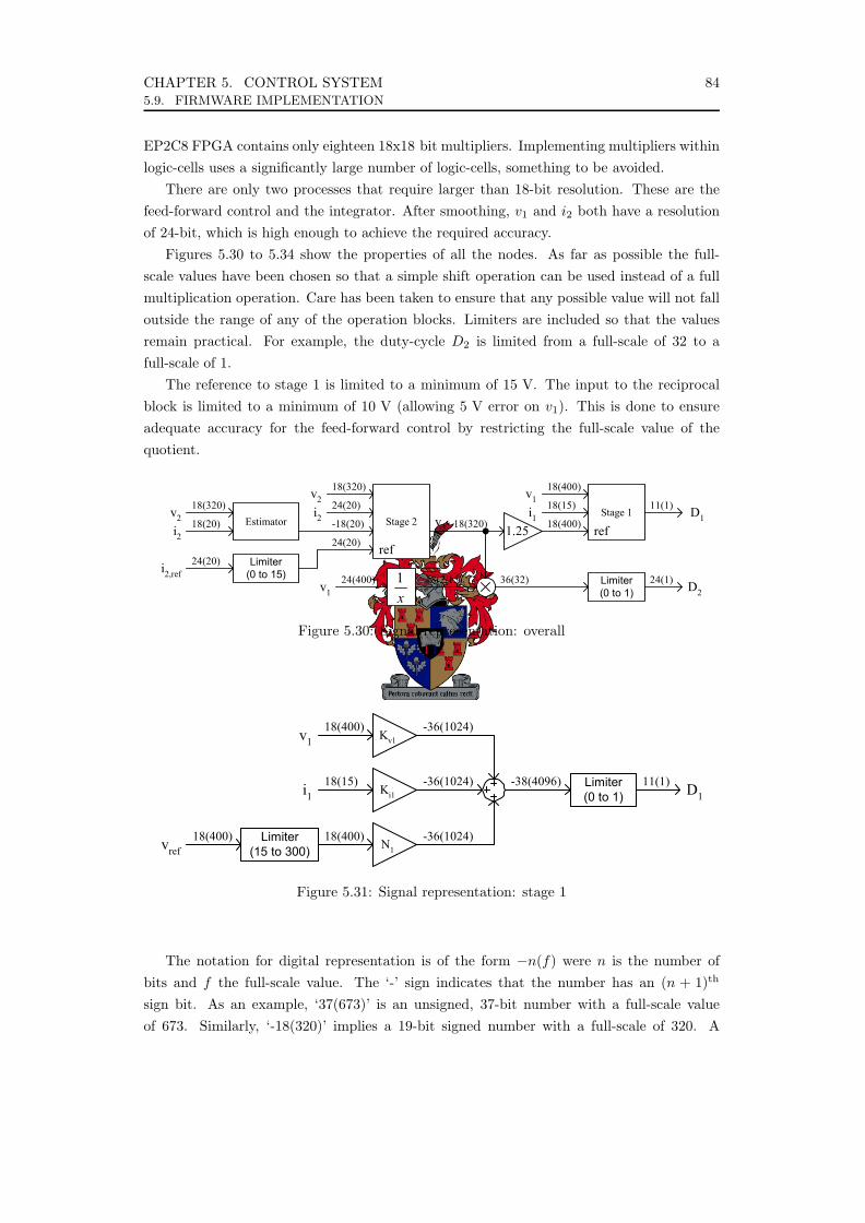
CHAPTER 5. CONTROL SYSTEM 845.9. FIRMWARE IMPLEMENTATION
EP2C8 FPGA contains only eighteen 18x18 bit multipliers. Implementing multipliers withinlogic-cells uses a significantly large number of logic-cells, something to be avoided.
There are only two processes that require larger than 18-bit resolution. These are thefeed-forward control and the integrator. After smoothing, v1 and i2 both have a resolutionof 24-bit, which is high enough to achieve the required accuracy.
Figures 5.30 to 5.34 show the properties of all the nodes. As far as possible the full-scale values have been chosen so that a simple shift operation can be used instead of a fullmultiplication operation. Care has been taken to ensure that any possible value will not falloutside the range of any of the operation blocks. Limiters are included so that the valuesremain practical. For example, the duty-cycle D2 is limited from a full-scale of 32 to afull-scale of 1.
The reference to stage 1 is limited to a minimum of 15 V. The input to the reciprocalblock is limited to a minimum of 10 V (allowing 5 V error on v1). This is done to ensureadequate accuracy for the feed-forward control by restricting the full-scale value of thequotient.
Chapter 5 – Control System : Firmware Implementation 76
large number of logic-cells, something to be avoided.
There are only two processes that require larger than 18-bit resolution. These are the feed-
forward control and the integrator. After smoothing, v1 and i2 both have a resolution of 24-bit, which is
high enough to achieve the required accuracy.
Figures 5.30 to 5.35 show the properties of all the nodes. As far as possible the full-scale values
have been chosen so that a simple shift operation can be used instead of a full multiplication operation.
Care has been taken to ensure that any possible value will not fall outside the range of any of the
operation blocks. Limiters are included so that the values remain practical. For example, the duty-
cycle D2 is limited from a full-scale of 32 to a full-scale of 1.
The reference to stage 1 is limited to a minimum of 15V. Also, the input to the reciprocal block is
limited to a minimum of 10V (allowing 5V error on v1). This is done to ensure adequate accuracy for
the feed-forward control by restricting the full-scale value of the quotient.
Limiter(0 to 1)
Estimator Stage 2Stage 1
1.25
i2,ref
i2
i1
v1v2 v3
i2
v2
v1 D2
D1
refref
x1
18(320)
18(20)
18(320)
24(20)
-18(20)
24(400)
11(1)
24(1)
18(320)
18(2/15)
18(400)
18(15)
18(400)
36(32)
Limiter(0 to 15)
24(20)
24(20)
Figure 5.30 – Signal sizes: overall
Ki1
RampLimiter
v1 Kv1
N1
i1
vref
D1
-36(1024)
-36(1024)
-36(1024)
-38(4096)
18(400)
18(15)
18(400)
18(400)
Limiter(0 to 1)
11(1)
Limiter(15 to 300)
18(400)
Figure 5.31 – Signal sizes: stage 1
Ki3
i2
N2
i3
iref
v3
Ki2
Kv2
RampLimiter ∫
Kint
v2
18(320)Limiter(0 to 300)
-38(1280)
-36(320)
-36(320)
-36(320)
-36(320)18(20)
-18(20)
18(20)
18(320)
-24(20)24(20)
24(20)
24(20)
24(20)
Figure 5.30: Signal representation: overall
Chapter 1 – Control System : Firmware Implementation 26
large number of logic-cells, something to be avoided.
There are only two processes that require larger than 18-bit resolution. These are the feed-
forward control and the integrator. After smoothing, v1 and i2 both have a resolution of 24-bit, which is
high enough to achieve the required accuracy.
Figures 5.30 to 5.35 show the properties of all the nodes. As far as possible the full-scale values
have been chosen so that a simple shift operation can be used instead of a full multiplication operation.
Care has been taken to ensure that any possible value will not fall outside the range of any of the
operation blocks. Limiters are included so that the values remain practical. For example, the duty-
cycle D2 is limited from a full-scale of 32 to a full-scale of 1.
The reference to stage 1 is limited to a minimum of 15V. Also, the input to the reciprocal block is
limited to a minimum of 10V (allowing 5V error on v1). This is done to ensure adequate accuracy for
the feed-forward control by restricting the full-scale value of the quotient.
Limiter(0 to 1)
Estimator Stage 2Stage 1
1.25
i2,ref
i2
i1
v1v2 v3
i2
v2
v1 D2
D1
refref
x1
18(320)
18(20)
18(320)
24(20)
-18(20)
24(400)
11(1)
24(1)
18(320)
18(2/15)
18(400)
18(15)
18(400)
36(32)
Limiter(0 to 15)
24(20)
24(20)
Figure 1.30 – Signal sizes: overall
Ki1
v1 Kv1
N1
i1
vref
D1
-36(1024)
-36(1024)
-36(1024)
-38(4096)
18(400)
18(15)
18(400)
Limiter(0 to 1)
11(1)
Limiter(15 to 300)
18(400)
Figure 1.31 – Signal sizes: stage 1
Ki3
i2
N2
i3
iref
v3
Ki2
Kv2
∫Kint
v2
18(320)Limiter(0 to 300)
-38(1280)
-36(320)
-36(320)
-36(320)
-36(320)18(20)
-18(20)
18(20)
18(320)
-24(20)24(20)
24(20)
24(20)
Figure 5.31: Signal representation: stage 1
The notation for digital representation is of the form −n(f) were n is the number ofbits and f the full-scale value. The ‘-’ sign indicates that the number has an (n + 1)th
sign bit. As an example, ‘37(673)’ is an unsigned, 37-bit number with a full-scale valueof 673. Similarly, ‘-18(320)’ implies a 19-bit signed number with a full-scale of 320. A

CHAPTER 5. CONTROL SYSTEM 855.9. FIRMWARE IMPLEMENTATION
Chapter 1 – Control System : Firmware Implementation 26
large number of logic-cells, something to be avoided.
There are only two processes that require larger than 18-bit resolution. These are the feed-
forward control and the integrator. After smoothing, v1 and i2 both have a resolution of 24-bit, which is
high enough to achieve the required accuracy.
Figures 5.30 to 5.35 show the properties of all the nodes. As far as possible the full-scale values
have been chosen so that a simple shift operation can be used instead of a full multiplication operation.
Care has been taken to ensure that any possible value will not fall outside the range of any of the
operation blocks. Limiters are included so that the values remain practical. For example, the duty-
cycle D2 is limited from a full-scale of 32 to a full-scale of 1.
The reference to stage 1 is limited to a minimum of 15V. Also, the input to the reciprocal block is
limited to a minimum of 10V (allowing 5V error on v1). This is done to ensure adequate accuracy for
the feed-forward control by restricting the full-scale value of the quotient.
Limiter(0 to 1)
Estimator Stage 2Stage 1
1.25
i2,ref
i2
i1
v1v2 v3
i2
v2
v1 D2
D1
refref
x1
18(320)
18(20)
18(320)
24(20)
-18(20)
24(400)
11(1)
24(1)
18(320)
18(2/15)
18(400)
18(15)
18(400)
36(32)
Limiter(0 to 15)
24(20)
24(20)
Figure 1.30 – Signal sizes: overall
Ki1
v1 Kv1
N1
i1
vref
D1
-36(1024)
-36(1024)
-36(1024)
-38(4096)
18(400)
18(15)
18(400)
Limiter(0 to 1)
11(1)
Limiter(15 to 300)
18(400)
Figure 1.31 – Signal sizes: stage 1
Ki3
i2
N2
i3
iref
v3
Ki2
Kv2
∫Kint
v2
18(320)Limiter(0 to 300)
-38(1280)
-36(320)
-36(320)
-36(320)
-36(320)18(20)
-18(20)
18(20)
18(320)
-24(20)24(20)
24(20)
24(20)
Figure 5.32: Signal representation: stage 2
Chapter 5 – Control System : Firmware Implementation 77
Figure 5.32 – Signal sizes: stage 2
Clock
Gint Out43(40) Limiter(0 to 18)
LatchDQ
42(20)
42(20)
24(20) 42(20) 18(20)
42(20)
In
tKG ∆= intint
Figure 5.33 – Signal sizes: integrator
v2 i3
i2
tC∆
2
18(400)
Limiter(-20 to 20)
LatchD Q
18(400) -18(400) -36(1280) -36(1280) -18(20)
18(20)
Clock
Figure 5.34 – Signal sizes: estimator
Out18(f)
LatchDQ
Limiter(-R to R)In 18(f)
18(f)
Clock
18(f)18(f)
Figure 5.35 – Signal sizes: ramp limiter
The notation for digital representation is of the form ‘-n(f)’ were ‘n’ is the number of bits and ‘f’
the full-scale value. The sign indicates that the number has an (n+1)th sign bit. As an example,
‘37(673)’ is an unsigned, 37-bit number with a full-scale value of 673. Similarly, ‘-18(320)’ implies a
19-bit signed number with a full-scale of 320. A signed number is in two’s compliment form when it is
an input to an adder. Inputs to a multiplier are represented differently – the most significant bit is the
sign and the remaining bits represent the magnitude. Conversions are performed between adder and
multiplier blocks.
The duty-cycle of stage 2 (D2) has been implemented as having a resolution of 24-bit. When
using the delay-line, the effective duty-cycle is still only 18-bit. Using the 24-bit resolution is only
possible with the noise-shaper (chapter 6).
Figure 5.33: Signal representation: integrator
Chapter 5 – Control System : Firmware Implementation 77
Figure 5.32 – Signal sizes: stage 2
Clock
Gint Out43(40) Limiter(0 to 18)
LatchDQ
42(20)
42(20)
24(20) 42(20) 18(20)
42(20)
In
tKG ∆= intint
Figure 5.33 – Signal sizes: integrator
v2 i3
i2
tC∆
2
18(400)
Limiter(-20 to 20)
LatchD Q
18(400) -18(400) -36(1280) -36(1280) -18(20)
18(20)
Clock
Figure 5.34 – Signal sizes: estimator
Out18(f)
LatchDQ
Limiter(-R to R)In 18(f)
18(f)
Clock
18(f)18(f)
Figure 5.35 – Signal sizes: ramp limiter
The notation for digital representation is of the form ‘-n(f)’ were ‘n’ is the number of bits and ‘f’
the full-scale value. The sign indicates that the number has an (n+1)th sign bit. As an example,
‘37(673)’ is an unsigned, 37-bit number with a full-scale value of 673. Similarly, ‘-18(320)’ implies a
19-bit signed number with a full-scale of 320. A signed number is in two’s compliment form when it is
an input to an adder. Inputs to a multiplier are represented differently – the most significant bit is the
sign and the remaining bits represent the magnitude. Conversions are performed between adder and
multiplier blocks.
The duty-cycle of stage 2 (D2) has been implemented as having a resolution of 24-bit. When
using the delay-line, the effective duty-cycle is still only 18-bit. Using the 24-bit resolution is only
possible with the noise-shaper (chapter 6).
Figure 5.34: Signal representation: estimator
signed number is in two’s complement form when it is an input to an adder. Inputs to amultiplier are represented differently – the most significant bit is the sign and the remainingbits represent the magnitude. Conversion between the two forms are performed betweenadder and multiplier blocks.
The duty-cycle of stage 2 (D2) has been implemented as having a resolution of 24-bit.When using the delay-line, the effective duty-cycle is still only 18-bit. Using the 24-bitresolution is only possible with the noise-shaper (chapter 6).
The digital representation (d) of a real number (r) is provided by equation 5.59.
d =r · 2n
f(5.59)
From this it is easy to deduce the digital representation of the constants. Figure 5.35shows a gain block. The gain of 2 thus has a digital representation that is 4 bits wide and
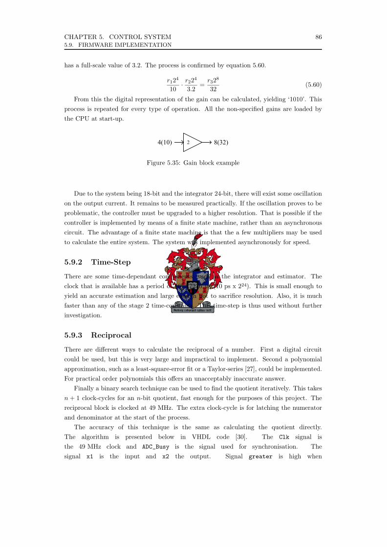
CHAPTER 5. CONTROL SYSTEM 865.9. FIRMWARE IMPLEMENTATION
has a full-scale value of 3.2. The process is confirmed by equation 5.60.
r124
10· r224
3.2=
r328
32(5.60)
From this the digital representation of the gain can be calculated, yielding ‘1010’. Thisprocess is repeated for every type of operation. All the non-specified gains are loaded bythe CPU at start-up.
Chapter 5 – Control System : Firmware Implementation 78
The digital representation (d) of a real number (r) is provided by formula 5.51.
frd
n2⋅= (5.51)
From this it is easy to deduce the digital representation of the constants. Figure 5.36 shows a gain
block. The gain of 2 thus has a digital representation that is 4 bits wide and has a full-scale value of
3.2. From this the digital representation of the gain can be calculated, yielding ‘1010’. This process is
repeated for every type of operation.
8(32)24(10)
Figure 5.36 – Gain block example
All the non-specified gains and ramp limiters are loaded by the CPU at start-up.
Due to the system being 18-bit and the integrator 24-bit, there will exist some oscillation on the
output current. It remains to be measured practically. If the oscillation proves to be problematic, the
controller must be upgraded to a higher resolution. That is possible if the controller is implemented by
means of a finite-state machine, rather than an asynchronous circuit. The advantage of a finite state
machine is that the same few multipliers may be used to calculate the entire system. The system was
implemented asynchronously for speed.
5.6.2 Time-Step There are some time-dependant components, such as the integrator, estimator and ramp-limiters.
The clock that is available has a period of 167.77216µs (10ps x 224). This is small enough to yield an
accurate estimation and large enough not to sacrifice resolution. Also, it is much faster than any of the
stage 2 time-constants. This time-step is thus used without further investigation.
5.6.3 Reciprocal There are different ways to calculate the reciprocal of a number. First a digital circuit could be
used, but this is very large and impractical to implement. Second a polynomial approximation, such as
a least-square-error fit or a Taylor-series [27], could be implemented. For practical order polynomials
this offers an unacceptably inaccurate answer.
Finally a binary search technique can be used to find the quotient iteratively. This takes n+1
clock-cycles for an n-bit quotient, fast enough for the purposes of this project. The reciprocal block is
clocked at 49kHz. The extra clock-cycle is for latching the numerator and denominator at the start of
the process.
Figure 5.35: Gain block example
Due to the system being 18-bit and the integrator 24-bit, there will exist some oscillationon the output current. It remains to be measured practically. If the oscillation proves to beproblematic, the controller must be upgraded to a higher resolution. That is possible if thecontroller is implemented by means of a finite state machine, rather than an asynchronouscircuit. The advantage of a finite state machine is that the a few multipliers may be usedto calculate the entire system. The system was implemented asynchronously for speed.
5.9.2 Time-Step
There are some time-dependant components, such as the integrator and estimator. Theclock that is available has a period of 167.77216 µs (10 ps x 224). This is small enough toyield an accurate estimation and large enough not to sacrifice resolution. Also, it is muchfaster than any of the stage 2 time-constants. This time-step is thus used without furtherinvestigation.
5.9.3 Reciprocal
There are different ways to calculate the reciprocal of a number. First a digital circuitcould be used, but this is very large and impractical to implement. Second a polynomialapproximation, such as a least-square-error fit or a Taylor-series [27], could be implemented.For practical order polynomials this offers an unacceptably inaccurate answer.
Finally a binary search technique can be used to find the quotient iteratively. This takesn + 1 clock-cycles for an n-bit quotient, fast enough for the purposes of this project. Thereciprocal block is clocked at 49 MHz. The extra clock-cycle is for latching the numeratorand denominator at the start of the process.
The accuracy of this technique is the same as calculating the quotient directly.The algorithm is presented below in VHDL code [30]. The Clk signal isthe 49 MHz clock and ADC_Busy is the signal used for synchronisation. Thesignal x1 is the input and x2 the output. Signal greater is high when
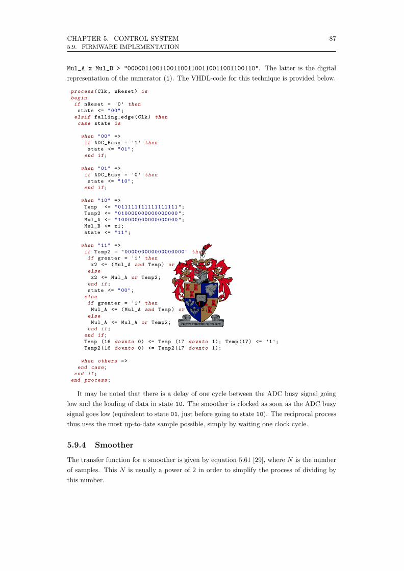
CHAPTER 5. CONTROL SYSTEM 875.9. FIRMWARE IMPLEMENTATION
Mul_A x Mul_B > "000001100110011001100110011001100110". The latter is the digitalrepresentation of the numerator (1). The VHDL-code for this technique is provided below.
process(Clk, nReset) is
begin
if nReset = '0' then
state <= "00";
elsif falling_edge(Clk) then
case state is
when "00" =>
if ADC_Busy = '1' then
state <= "01";
end if;
when "01" =>
if ADC_Busy = '0' then
state <= "10";
end if;
when "10" =>
Temp <= "011111111111111111";
Temp2 <= "010000000000000000";
Mul_A <= "100000000000000000";
Mul_B <= x1;
state <= "11";
when "11" =>
if Temp2 = "000000000000000000" then
if greater = '1' then
x2 <= (Mul_A and Temp) or Temp2;
else
x2 <= Mul_A or Temp2;
end if;
state <= "00";
else
if greater = '1' then
Mul_A <= (Mul_A and Temp) or Temp2;
else
Mul_A <= Mul_A or Temp2;
end if;
end if;
Temp (16 downto 0) <= Temp (17 downto 1); Temp(17) <= '1';Temp2(16 downto 0) <= Temp2(17 downto 1);
when others =>
end case;
end if;
end process;
It may be noted that there is a delay of one cycle between the ADC busy signal goinglow and the loading of data in state 10. The smoother is clocked as soon as the ADC busysignal goes low (equivalent to state 01, just before going to state 10). The reciprocal processthus uses the most up-to-date sample possible, simply by waiting one clock cycle.
5.9.4 Smoother
The transfer function for a smoother is given by equation 5.61 [29], where N is the numberof samples. This N is usually a power of 2 in order to simplify the process of dividing bythis number.
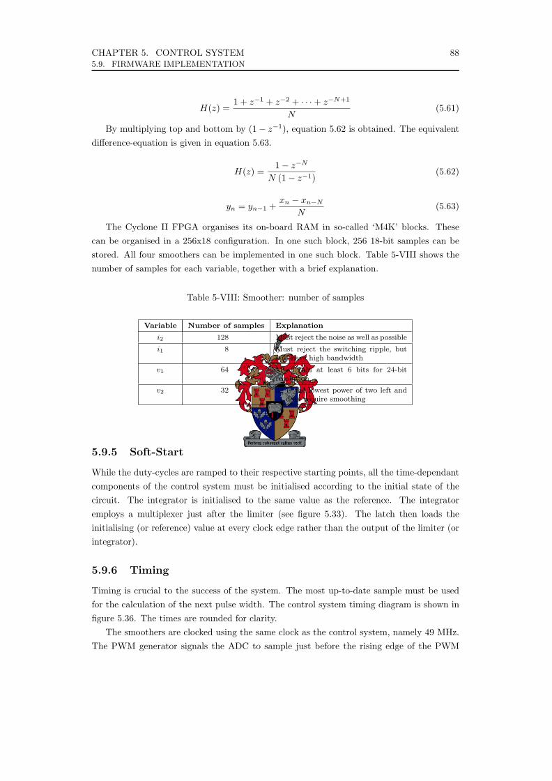
CHAPTER 5. CONTROL SYSTEM 885.9. FIRMWARE IMPLEMENTATION
H(z) =1 + z−1 + z−2 + · · ·+ z−N+1
N(5.61)
By multiplying top and bottom by (1− z−1), equation 5.62 is obtained. The equivalentdifference-equation is given in equation 5.63.
H(z) =1− z−N
N (1− z−1)(5.62)
yn = yn−1 +xn − xn−N
N(5.63)
The Cyclone II FPGA organises its on-board RAM in so-called ‘M4K’ blocks. Thesecan be organised in a 256x18 configuration. In one such block, 256 18-bit samples can bestored. All four smoothers can be implemented in one such block. Table 5-VIII shows thenumber of samples for each variable, together with a brief explanation.
Table 5-VIII: Smoother: number of samples
Variable Number of samples Explanation
i2 128 Must reject the noise as well as possible
i1 8 Must reject the switching ripple, butstill have high bandwidth
v1 64 Must gain at least 6 bits for 24-bitresolution
v2 32 32 is the lowest power of two left andv2 does require smoothing
5.9.5 Soft-Start
While the duty-cycles are ramped to their respective starting points, all the time-dependantcomponents of the control system must be initialised according to the initial state of thecircuit. The integrator is initialised to the same value as the reference. The integratoremploys a multiplexer just after the limiter (see figure 5.33). The latch then loads theinitialising (or reference) value at every clock edge rather than the output of the limiter (orintegrator).
5.9.6 Timing
Timing is crucial to the success of the system. The most up-to-date sample must be usedfor the calculation of the next pulse width. The control system timing diagram is shown infigure 5.36. The times are rounded for clarity.
The smoothers are clocked using the same clock as the control system, namely 49 MHz.The PWM generator signals the ADC to sample just before the rising edge of the PWM
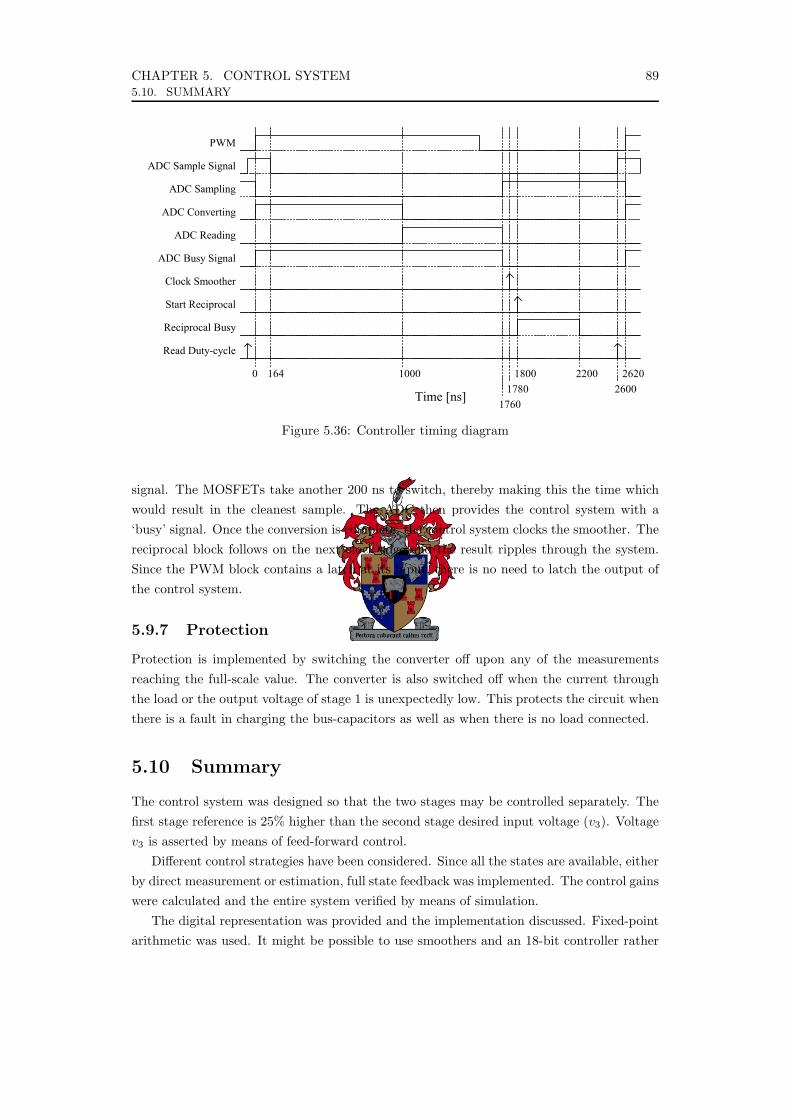
CHAPTER 5. CONTROL SYSTEM 895.10. SUMMARY
Chapter 5 – Control System : Firmware Implementation 81
initialised to the same value as the reference. This is performed by inserting multiplexers. The
integrator, for example, employs a multiplexer just after the limiter.
5.6.6 Timing Timing is crucial to the success of the system. The most up-to-date sample must be used for the
calculation of the next pulse width. The control system timing diagram is shown in figure 5.37. The
times are rounded for clarity.
PWM
ADC Sample Signal
ADC Sampling
ADC Converting
ADC Reading
ADC Busy Signal
Clock Smoother
Start Reciprocal
Read Duty-cycle
Reciprocal Busy
0
Time [ns]
1000164
17601780
1800 22002600
2620
Figure 5.37 – Controller timing diagram
The smoothers are clocked using the same clock as the control system, namely 49MHz. The
PWM generator signals the ADC to sample just before the rising edge of the PMW signal. The
MOSFETs take another 200ns to switch, thereby making this the time which would result in the
cleanest sample. The ADC then provides the control system with a ‘busy’ signal. Once the conversion
is complete, the control system clocks the smoother. The reciprocal block follows on the next clock
edge and the result ripples through the system. Since the PWM block contains a latch at its input, there
is no need to latch the output of the control system.
5.6.7 Protection Protection is implemented by switching the converter off upon any of the measurements reaching
the full-scale value. The converter is also switched off when the current through the load or the output
voltage of stage 1 is unexpectedly low. This protects the circuit when there is a fault in charging the
bus-capacitors as well as when there is no load connected.
Figure 5.36: Controller timing diagram
signal. The MOSFETs take another 200 ns to switch, thereby making this the time whichwould result in the cleanest sample. The ADC then provides the control system with a‘busy’ signal. Once the conversion is complete, the control system clocks the smoother. Thereciprocal block follows on the next clock edge and the result ripples through the system.Since the PWM block contains a latch at its input, there is no need to latch the output ofthe control system.
5.9.7 Protection
Protection is implemented by switching the converter off upon any of the measurementsreaching the full-scale value. The converter is also switched off when the current throughthe load or the output voltage of stage 1 is unexpectedly low. This protects the circuit whenthere is a fault in charging the bus-capacitors as well as when there is no load connected.
5.10 Summary
The control system was designed so that the two stages may be controlled separately. Thefirst stage reference is 25% higher than the second stage desired input voltage (v3). Voltagev3 is asserted by means of feed-forward control.
Different control strategies have been considered. Since all the states are available, eitherby direct measurement or estimation, full state feedback was implemented. The control gainswere calculated and the entire system verified by means of simulation.
The digital representation was provided and the implementation discussed. Fixed-pointarithmetic was used. It might be possible to use smoothers and an 18-bit controller rather

CHAPTER 5. CONTROL SYSTEM 905.10. SUMMARY
than the proposed 24-bit controller and higher resolution ADCs. This remains to be verifiedexperimentally.

Chapter 6
Digital PWM
6.1 Introduction
In chapter 5 the control system was designed. The PWM resolution necessary to producesatisfactory results is impractical to implement directly. Two techniques for solving thisproblem are discussed in this chapter; they are the use of a delay-line and the implementationof a noise-shaper. The firmware implementation of both alternatives is presented.
6.2 Resolution
6.2.1 Required Resolution
The output of the converter needs to be controllable to at least 5 ppm in order to realise10 ppm stability. The equation for calculating the resolution (R) as a fraction of the outputvoltage, knowing the average duty-cycle (D) and bit-resolution (Rb), is given by equation6.1. The second stage average duty-cycle is 80%, which implies that a bit-resolution of 18-bitwould be required.
R =2−Rb
D(6.1)
The first stage does not need to be as accurate. The only requirement is that it attenuatesthe line-frequency ripple to some extent. Table 6-I gives the controllability with variousdifferent resolutions, assuming a bus voltage of 560 V.
The full-scale value of the ADC used to convert v1 is 400 V, as explained in chapter5. Its resolution is 18-bit, which translates to 1.526 mV. The leakage-inductance of thetransformer, however, results in an uncertainty in duty-cycle. From chapter 4 it wascalculated that the maximum uncertainty in duty-cycle at minimum load is 0.027% (notconsidering the effect of dead time). This is an uncertainty in output voltage of 153 mV,which corresponds to a PWM resolution of 12-bit. To make the system more deterministic,11-bit PWM was implemented.
91

CHAPTER 6. DIGITAL PWM 926.2. RESOLUTION
Table 6-I: Stage 1 PWM resolution
Resolution [bits] Controllability [mV]
8 2 187.50
9 1 093.75
10 546.88
11 273.44
12 136.72
13 68.36
14 34.18
15 17.09
16 8.55
17 4.27
18 2.14
19 1.07
20 0.53
21 0.27
6.2.2 Practical Digital PWM
When a PWM waveform is generated purely by comparing a reference to a counter, thesmallest step in pulse width is equal to the period of the clock that drives that counter. Thefastest clock that can drive a 16-bit counter in an Altera Cyclone II FPGA is (according tothe datasheet) 401.6 MHz. This drops to 157.15 MHz for a 64-bit counter.
As a rough estimate using linear interpolation (equation 6.2), an 18-bit counter wouldrequire a clock of 391.4 MHz. This would mean that 18-bit PWM can only be generated fora switching frequency of 1.493 kHz, which is unacceptably slow. Another method must befound.
f =(
(401.6− 157.15)(16− 64)
(Rb − 16) + 401.6)
MHz (6.2)
6.2.3 Delay-Line
By using a delay-line IC such as the MC10EP195 from ON Semiconductor, one can generatemuch higher resolution pulses. This IC can set the delay on a pulse from 2.20 ns to 12.23 ns in10 ps steps by means of a 10-bit ‘delay word’. This means that 18-bit PWM can be generatedat a switching frequency of 381.470 kHz by using a counter clock of only 97.656 MHz. Fromthis same counter, an 11-bit 47.684 kHz PWM signal can be generated for the first stage.
Another advantage of using a delay-line is that the effect of changing the duty-cycle isimmediate. A noise-shaper (described in the following section) has a bandwidth limitation.
The 10 ps delay is not exact though, and does give some small error on the pulse-width.According to the datasheet, resolution is typically between 9.78 ps and 10.7 ps, dependingon the temperature. The FPGA clock is only accurate to 50 ppm. The actual duty-cycle can

CHAPTER 6. DIGITAL PWM 936.2. RESOLUTION
be plotted against the required duty-cycle. The resulting worst-case graphs are presentedin figure 6.1.
(a) Slow delay-line (b) Fast delay-line
Figure 6.1: Duty-cycle error
There are three obvious solutions. The first is to ignore the error and let the controlsystem correct the it. The duty-cycle is adjustable in small steps, even though these steps donot follow exactly as planned. They are still close enough to 10 ps for all practical purposes.It is also only 0.1% of the duty-cycle that falls on a ‘glitch’.
Another more elegant solution is to utilise the fact that the FPGA uses a PLL togenerate its 195.3125 MHz clock. The possible PLL configurations (using a 125 MHzexternal oscillator) that result in a clock frequency within 10% are given in table 6-II.
Table 6-II: FPGA PLL configurations
Divide Multiply Frequency [MHz]
12 17 177.083
16 23 179.688
9 13 180.556
20 29 181.250
15 22 183.333
2 3 187.500
15 23 191.667
20 31 193.750
9 14 194.444
16 25 195.312
12 19 197.917
5 8 200.000
8 13 203.125
6 10 208.333
16 27 210.938
CHAPTER 6. DIGITAL PWM 946.3. NOISE-SHAPER
The final, most accurate solution is to use an external PLL with the divide andfeedback counters implemented inside the FPGA. This will give as much clock-adjustmentas is required. By using a far more stable 4 MHz crystal oscillator, a 10-bit dividecounter and a 16-bit feedback counter, the 195 MHz clock can be adjusted to the nearest3.906 kHz (102 fs).
The latter two options require calibration to match the delay-line at the normal operatingtemperature. This is a relatively complex process and thus the first option was chosen.
6.3 Noise-Shaper
6.3.1 Quantisation as a Noise Source
Rounding an n-bit signal to the nearest m-bit value adds a random error signal. The rangeof this error signal is given by equation 6.3, assuming unity full-scale [13].
e ∈(−2−(m+1); 2−(m+1)
](6.3)
It is possible to reconstruct the original signal by changing the quantisation method. Say,for example, a constant signal of 5.2 is quantised. Rounding the signal to 5 is equivalent toadding a constant error of -0.2. If, however, the signal is rounded to 6 for 20% of the timeand to 5 the other 80%, the average of the resulting signal is 5.2, equalling the original.
The duty-cycle is a signal that is constantly changing. The error signal is thusuncorrelated to both the PWM signal and the duty-cycle. According to the central limittheorem [28], the error signal is Gaussian in nature and has a flat frequency spectrum. Anoise-shaper is a signal processing technique by which the error signal, or noise, is frequency-shaped. Lower frequency noise power is moved to higher frequencies.
This approach is of course provided that the duty-cycle signal is significantly larger thanthe quantisation increment. In the presence of line-frequency ripple, this would be thecase, but at medium or minimum load the effect is not clear. Practical experimentation isrequired.
6.3.2 Block Diagram
Figure 6.2 shows the block diagram of a noise-shaper [13].As described in the previous section, quantisation can be modelled as an error signal
(e) being added to the input signal. Figure 6.3 shows the model, along with relevant signalnames [13].
The respective z-transforms of x, e and eo are X, E and Eo. Equations 6.4 and 6.5show the relationship between H(z) and the so-called “noise transfer function” or NTF(z).It can be shown that the optimal implementation of the noise transfer function is given byequation 6.6 where N is the order of the noise-shaper [13].
X + E0 = X − EH(z) + E (6.4)

CHAPTER 6. DIGITAL PWM 956.3. NOISE-SHAPER
Chapter 6 – Digital PWM : Noise-Shaper 87
It is possible to reconstruct the original signal by changing the quantisation method. Say, for
example, a constant signal of 5.2 is quantised. Rounding the signal to 5 is equivalent to adding a
constant error of -0.2. If, however, the signal is rounded to 6 for 20% of the time and to 5 the other
80%, the average of the resulting signal is 5.2, equalling the original.
The duty-cycle is a signal that is constantly changing. The error signal is thus uncorrelated to
both the PWM signal and the duty-cycle. According to the central limit theorem [20], the error signal is
Gaussian in nature and has a flat frequency spectrum. A noise-shaper is a signal processing technique
by which the error signal, or noise, is frequency-shaped. Lower frequency noise power is moved to
higher frequencies.
This approach is of course provided that the duty-cycle signal is significantly larger than the
quantisation increment. In the presence of line-frequency ripple, this would be the case, but at medium
or minimum load the effect is not clear. Practical experimentation is required.
6.2.2 Block Diagram Figure 6.2 shows the block-diagram of a noise-shaper.
Quantisation Out
H(z)
n n m
n-m
In
Figure 6.2 – Noise-shaper block diagram
As described in the previous section, quantisation can be modelled as an error signal (e) being
added to the input signal. Figure 6.3 shows the model, along with relevant signal names.
x+eo
H(z)
x
e
Figure 6.3 – Noise-shaper block diagram
The respective z-transforms of ‘x’, ‘e’ and ‘eo’ are ‘X’, ‘E’ and ‘Eo’. Equations 6.4 and 6.5 show
the relationship between H(z) and the so-called “noise transfer function” or NTF(z). It can be shown
that the optimal implementation of the noise transfer function is given by equation 6.6 where ‘N’ is the
order of the noise-shaper.
EzEHXEX o +−=+ )( (6.4)
Figure 6.2: Noise-shaper block diagram
Chapter 6 – Digital PWM : Noise-Shaper 87
It is possible to reconstruct the original signal by changing the quantisation method. Say, for
example, a constant signal of 5.2 is quantised. Rounding the signal to 5 is equivalent to adding a
constant error of -0.2. If, however, the signal is rounded to 6 for 20% of the time and to 5 the other
80%, the average of the resulting signal is 5.2, equalling the original.
The duty-cycle is a signal that is constantly changing. The error signal is thus uncorrelated to
both the PWM signal and the duty-cycle. According to the central limit theorem [20], the error signal is
Gaussian in nature and has a flat frequency spectrum. A noise-shaper is a signal processing technique
by which the error signal, or noise, is frequency-shaped. Lower frequency noise power is moved to
higher frequencies.
This approach is of course provided that the duty-cycle signal is significantly larger than the
quantisation increment. In the presence of line-frequency ripple, this would be the case, but at medium
or minimum load the effect is not clear. Practical experimentation is required.
6.2.2 Block Diagram Figure 6.2 shows the block-diagram of a noise-shaper.
Quantisation Out
H(z)
n n m
n-m
In
Figure 6.2 – Noise-shaper block diagram
As described in the previous section, quantisation can be modelled as an error signal (e) being
added to the input signal. Figure 6.3 shows the model, along with relevant signal names.
x+eo
H(z)
x
e
Figure 6.3 – Noise-shaper block diagram
The respective z-transforms of ‘x’, ‘e’ and ‘eo’ are ‘X’, ‘E’ and ‘Eo’. Equations 6.4 and 6.5 show
the relationship between H(z) and the so-called “noise transfer function” or NTF(z). It can be shown
that the optimal implementation of the noise transfer function is given by equation 6.6 where ‘N’ is the
order of the noise-shaper.
EzEHXEX o +−=+ )( (6.4)
Figure 6.3: Noise-shaper block diagram
NTF (z) =E0
E= 1−H(z) (6.5)
NTF (z) =(
z − 1z
)N
(6.6)
The effect is thus that the noise added by quantisation is shaped by the noise transferfunction before being added to the ideal output.
6.3.3 Theory of Operation
From the previous section it can seen that the signal passes through directly, but withadded noise. By substituting equation 6.7 into equation 6.6, the frequency response of thenoise transfer function is obtained [13]. This is shown in equation 6.8. The noise is thusshaped according to equation 6.9 where f is the frequency in question and fs the switchingfrequency. The phase is given by equation 6.10.
z = ej2π ffs (6.7)
NTF (f) =[1− cos
(2πf
fs
)+ j sin
(2πf
fs
)]N
(6.8)
|NTF (f)| =[2 sin
(πf
fs
)]N
(6.9)
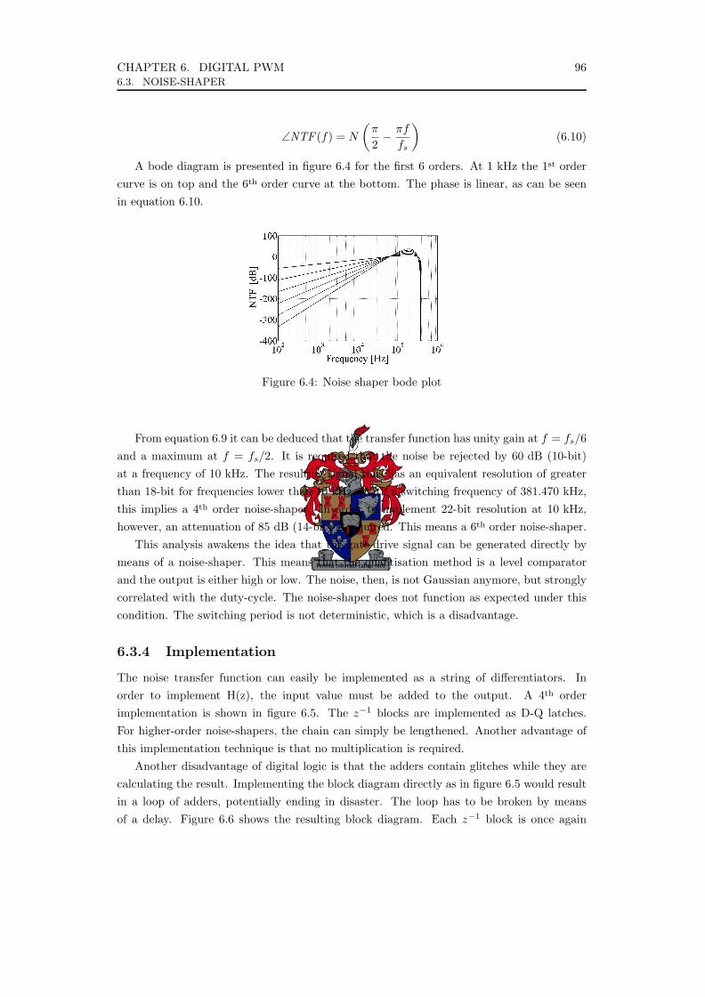
CHAPTER 6. DIGITAL PWM 966.3. NOISE-SHAPER
∠NTF (f) = N
(π
2− πf
fs
)(6.10)
A bode diagram is presented in figure 6.4 for the first 6 orders. At 1 kHz the 1st ordercurve is on top and the 6th order curve at the bottom. The phase is linear, as can be seenin equation 6.10.
Figure 6.4: Noise shaper bode plot
From equation 6.9 it can be deduced that the transfer function has unity gain at f = fs/6and a maximum at f = fs/2. It is required that the noise be rejected by 60 dB (10-bit)at a frequency of 10 kHz. The resulting signal thus has an equivalent resolution of greaterthan 18-bit for frequencies lower than 10 kHz. With a switching frequency of 381.470 kHz,this implies a 4th order noise-shaper. In order to implement 22-bit resolution at 10 kHz,however, an attenuation of 85 dB (14-bit) is required. This means a 6th order noise-shaper.
This analysis awakens the idea that the gate-drive signal can be generated directly bymeans of a noise-shaper. This means that the quantisation method is a level comparatorand the output is either high or low. The noise, then, is not Gaussian anymore, but stronglycorrelated with the duty-cycle. The noise-shaper does not function as expected under thiscondition. The switching period is not deterministic, which is a disadvantage.
6.3.4 Implementation
The noise transfer function can easily be implemented as a string of differentiators. Inorder to implement H(z), the input value must be added to the output. A 4th orderimplementation is shown in figure 6.5. The z−1 blocks are implemented as D-Q latches.For higher-order noise-shapers, the chain can simply be lengthened. Another advantage ofthis implementation technique is that no multiplication is required.
Another disadvantage of digital logic is that the adders contain glitches while they arecalculating the result. Implementing the block diagram directly as in figure 6.5 would resultin a loop of adders, potentially ending in disaster. The loop has to be broken by meansof a delay. Figure 6.6 shows the resulting block diagram. Each z−1 block is once again

CHAPTER 6. DIGITAL PWM 976.3. NOISE-SHAPER
Chapter 6 – Digital PWM : Noise-Shaper 89
6.2.4 Implementation The noise transfer function can easily be implemented as a string of differentiators. In order to
implement H(z), the input value must be added to the output. A 4th order implementation is shown in
figure 6.4. The ‘z-1’ blocks are implemented as D-Q latches. For higher-order noise-shapers, the chain
can simply be lengthened. Another advantage of this implementation technique is that no
multiplication is required.
OutIn
z-1z-1 z-1z-1
Figure 6.4 – Noise-shaper H(z) implementation
Another disadvantage of digital logic is that the adders contain glitches while they are calculating
the result. Implementing the block diagram directly as in figure 6.3 would result in a loop of adders,
potentially ending in disaster. The loop has to be broken by means of a delay. Figure 6.5 shows the
resulting block diagram. Each ‘z-1’ block is once again implemented as a D-Q latch. Rounding is
performed by adding bit 9 to the 8-bit word obtained from bits 10 to 17 (bit 0 is the least significant and
bit 17 the most).
8-bit out18-bit in
z-1z-1z-1z-1
Round to nearest8-bit value
z-1
Figure 6.5 – Noise-shaper implementation
From the noise transfer function it may be noted that the DC component of the noise is removed
completely. It is easier to floor digitally than to round digitally. Also, the error is available
immediately, i.e. the least significant bits. The ‘round to nearest 8-bit value’ block may thus be
replaced with a ‘truncate’ block without a decrease in performance.
Figure 6.5: Noise-shaper H(z) implementation
implemented as a D-Q latch. Rounding is performed by adding bit 9 to the 8-bit wordobtained from bits 10 to 17 (bit 0 is the least significant and bit 17 the most).
Chapter 6 – Digital PWM : Noise-Shaper 89
6.2.4 Implementation The noise transfer function can easily be implemented as a string of differentiators. In order to
implement H(z), the input value must be added to the output. A 4th order implementation is shown in
figure 6.4. The ‘z-1’ blocks are implemented as D-Q latches. For higher-order noise-shapers, the chain
can simply be lengthened. Another advantage of this implementation technique is that no
multiplication is required.
OutIn
z-1z-1 z-1z-1
Figure 6.4 – Noise-shaper H(z) implementation
Another disadvantage of digital logic is that the adders contain glitches while they are calculating
the result. Implementing the block diagram directly as in figure 6.3 would result in a loop of adders,
potentially ending in disaster. The loop has to be broken by means of a delay. Figure 6.5 shows the
resulting block diagram. Each ‘z-1’ block is once again implemented as a D-Q latch. Rounding is
performed by adding bit 9 to the 8-bit word obtained from bits 10 to 17 (bit 0 is the least significant and
bit 17 the most).
8-bit out18-bit in
z-1z-1z-1z-1
Round to nearest8-bit value
z-1
Figure 6.5 – Noise-shaper implementation
From the noise transfer function it may be noted that the DC component of the noise is removed
completely. It is easier to floor digitally than to round digitally. Also, the error is available
immediately, i.e. the least significant bits. The ‘round to nearest 8-bit value’ block may thus be
replaced with a ‘truncate’ block without a decrease in performance.
Figure 6.6: Noise-shaper implementation
From the noise transfer function it may be noted that the DC component of the noiseis removed completely. It is easier to floor digitally than to round digitally. Also, the erroris available immediately, i.e. the least significant bits. The ‘round to nearest 8-bit value’block may thus be replaced with a ‘truncate’ block without a decrease in performance.
6.3.5 Performance
The system in figure 6.6 was implemented in MATLAB [31] (with flooring as apposed torounding) and simulated with a 5 kHz, 1 Vp-p sinusoidal input signal. Figure 6.7 shows theresults.
It seems as though the noise-shaper worsens the signal. It must be remembered, though,that the noise-shaper attenuates the low-frequency noise by increasing the high-frequencynoise. Figure 6.8 shows the same peak after passing all three signals through the samelow-pass filter. This filter is equivalent to the second-order LC filter designed for stage 2 inthe previous chapter.
From these graphs it is clear that the noise-shaper performs well. The error evident inthe 8-bit signal is completely removed. It is also interesting to note that it adds negligibledelay to the input signal.
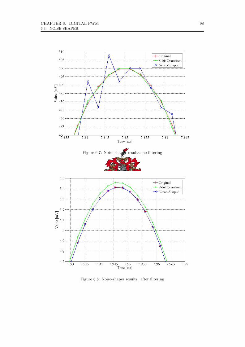
CHAPTER 6. DIGITAL PWM 986.3. NOISE-SHAPER
Figure 6.7: Noise-shaper results: no filtering
Figure 6.8: Noise-shaper results: after filtering
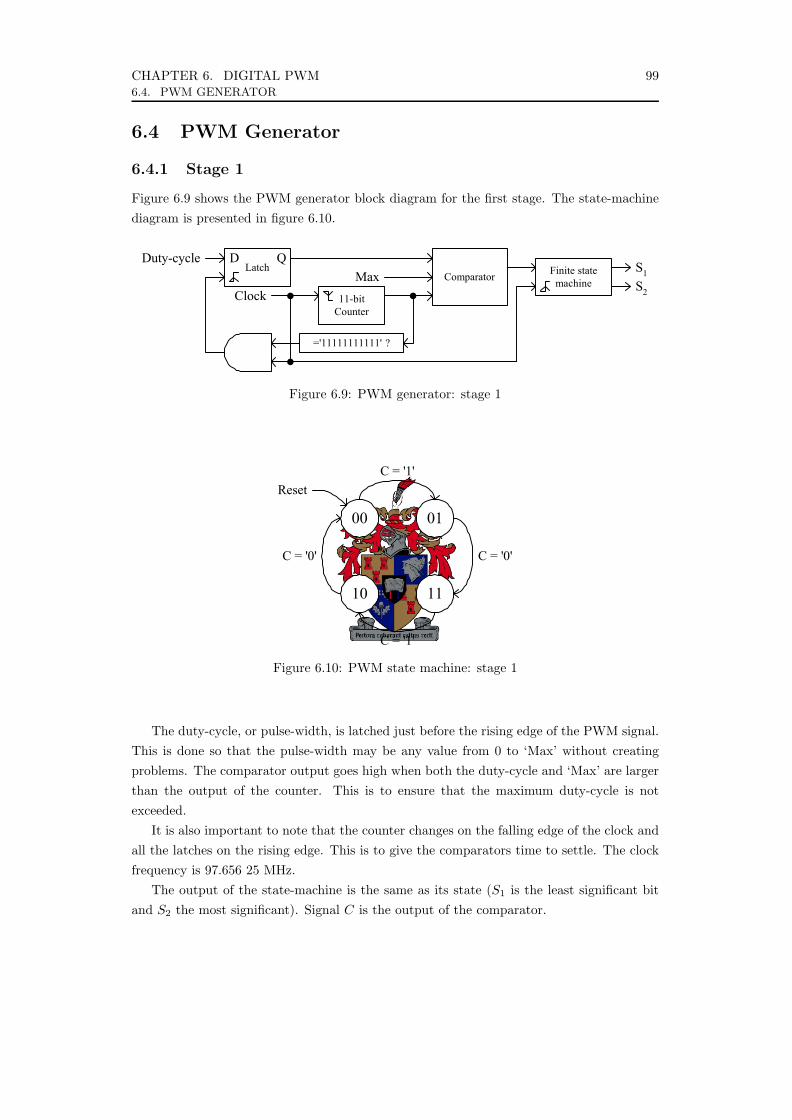
CHAPTER 6. DIGITAL PWM 996.4. PWM GENERATOR
6.4 PWM Generator
6.4.1 Stage 1
Figure 6.9 shows the PWM generator block diagram for the first stage. The state-machinediagram is presented in figure 6.10.
Chapter 6 – Digital PWM : PWM Generator 91
Figure 6.7 – Noise-shaper results: after filtering
From these graphs it is clear that the noise-shaper performs well. It is also interesting to note that
it adds negligible delay to the input signal.
6.3 PWM Generator 6.3.1 Stage 1
Figure 6.8 shows the PWM generator block diagram for the first stage. The state-machine
diagram is presented in figure 6.9.
S1Duty-cycle
11-bitCounter
ComparatorMax
='11111111111' ?
LatchD Q
Clock
Finite statemachine S2
Figure 6.8 – PWM generator: stage 1
Figure 6.9: PWM generator: stage 1
Chapter 6 – Digital PWM : PWM Generator 92
00 01
1110
ResetC = '1'
C = '1'
C = '0'C = '0'
Figure 6.9 – PWM state machine: stage 1
The duty-cycle, or pulse-width, is latched just before the rising edge of the PWM signal. This is
done so that the pulse-width may be any value from 0 to ‘Max’ without creating problems. The
comparator output goes high when both the duty-cycle and ‘Max’ are larger than the output of the
counter. This is to ensure that the maximum duty-cycle is not exceeded.
It is also important to note that the counter changes on the falling edge of the clock and all the
latches on the rising edge. This is to give the comparators time to settle. The clock frequency is
97.65625MHz.
The output of the state-machine is the same as its state (S1 is the least significant bit and S2 the
most significant). Signal ‘C’ is the output of the comparator.
6.3.2 Stage 2 Figure 6.10 shows the block-diagram of the second stage PWM generator, including a delay-line.
For the case where a noise-shaper is used instead, the control system incorporates the noise-shaper and
the implementation below excludes the splitter and delay circuit.
Splitter PWMDuty-cycle
8-bitCounter
DelayD
Qdt
LatchD Q
ComparatorMax
AB
='11111111' ?
LatchD Q
Clock
0
1
Noise shaper on
1
0
Noise-ShaperH(z)
Figure 6.10 – PWM generator: stage 2
Signal ‘A’ is the least significant ten bits of the duty-cycle and signal ‘B’ the most significant
eight. The comparator is similar as in stage 1 – the only difference is that this one is 8-bit.
Figure 6.10: PWM state machine: stage 1
The duty-cycle, or pulse-width, is latched just before the rising edge of the PWM signal.This is done so that the pulse-width may be any value from 0 to ‘Max’ without creatingproblems. The comparator output goes high when both the duty-cycle and ‘Max’ are largerthan the output of the counter. This is to ensure that the maximum duty-cycle is notexceeded.
It is also important to note that the counter changes on the falling edge of the clock andall the latches on the rising edge. This is to give the comparators time to settle. The clockfrequency is 97.656 25 MHz.
The output of the state-machine is the same as its state (S1 is the least significant bitand S2 the most significant). Signal C is the output of the comparator.

CHAPTER 6. DIGITAL PWM 1006.5. SUMMARY
6.4.2 Stage 2
Figure 6.11 shows the block diagram of the second stage PWM generator, including a delay-line. For the case where a noise-shaper is used instead, the control system incorporates thenoise-shaper and the implementation below excludes the splitter and delay circuit.
Chapter 6 – Digital PWM : PWM Generator 92
00 01
1110
ResetC = '1'
C = '1'
C = '0'C = '0'
Figure 6.9 – PWM state machine: stage 1
The duty-cycle, or pulse-width, is latched just before the rising edge of the PWM signal. This is
done so that the pulse-width may be any value from 0 to ‘Max’ without creating problems. The
comparator output goes high when both the duty-cycle and ‘Max’ are larger than the output of the
counter. This is to ensure that the maximum duty-cycle is not exceeded.
It is also important to note that the counter changes on the falling edge of the clock and all the
latches on the rising edge. This is to give the comparators time to settle. The clock frequency is
97.65625MHz.
The output of the state-machine is the same as its state (S1 is the least significant bit and S2 the
most significant). Signal ‘C’ is the output of the comparator.
6.3.2 Stage 2 Figure 6.10 shows the block-diagram of the second stage PWM generator, including a delay-line.
For the case where a noise-shaper is used instead, the control system incorporates the noise-shaper and
the implementation below excludes the splitter and delay circuit.
Splitter PWMDuty-cycle
8-bitCounter
DelayD
Qdt
LatchD Q
ComparatorMax
AB
='11111111' ?
LatchD Q
Clock
0
1
Noise shaper on
1
0
Noise-ShaperH(z)
Figure 6.10 – PWM generator: stage 2
Signal ‘A’ is the least significant ten bits of the duty-cycle and signal ‘B’ the most significant
eight. The comparator is similar as in stage 1 – the only difference is that this one is 8-bit.
Figure 6.11: PWM generator: stage 2
Signal A is the least significant ten bits of the duty-cycle and signal B the most significanteight. The comparator is similar as in stage 1 – the only difference is that this one is 8-bit.
Also similar to the first stage, the counter changes on the falling edge of the clock andall the latches on the rising edge. The clock frequency is also 97.656 25 MHz.
The delay-line’s delay word is zero when the PWM signal is low and equal to the leastsignificant ten bits of the duty-cycle when the PWM signal is high. This is to delay onlythe falling edge, thus producing the correct pulse-width. The delay-line circuit is disabledwhen the noise shaper is active.
6.5 Summary
Although high-resolution PWM is difficult to implement digitally, at least two techniquesexist which solve the problem. These are the delay-line and the noise-shaper. Uncertaintiesregarding the performance of both techniques may be clarified through experimentation. Thedelay-line does not provide the predicted duty-cycle exactly and the noise-shaper may notfunction properly with small signals. Both of the above techniques have been implementedwith a signal allocated to switch between them.
Chapter 7
Probe
7.1 Introduction
In appendix C the physics behind NMR are described. It is strongly suggested that this beperused prior to reading this chapter in order to gain a better understanding of the processesinvolved.
This chapter proposes a new NMR magnetometer concept and confirms it throughsimulation. Much research remains to be done in this area.
Practical aspects are discussed and recommendations made, although a workingprototype is not available. Measurements are included regarding the performance of thehardware. No NMR effects were tested practically.
7.2 Phase-Locked Loop NMR
7.2.1 Principle of Operation
As mentioned in appendix C, the steady state My is given by equation 7.1. The maximumvalue for My occurs when the denominator is equal to 2. At that point the excitation signalBx is approximately 910 pT and My is 0.57·M0.
My =M0γBxT2
1 + γ2B2xT1T2
(7.1)
When the detection- and excitation coil is wound at right-angles with each other, thecoupling between them is small. It is then possible to have a continuous excitation signaland still detect the magnetisation vector.
A small error in excitation frequency will result in a rapid shift in phase between theexcitation and detected signals. This phase can then be used to correct the frequency ofexcitation. The short-term immediate phase at time t1 can be calculated using equation7.2. Here φ0 is the phase at time zero. A phase-locked loop may then be used to force thephase to zero. The resulting frequency of the oscillator resembles the field-strength.
101
CHAPTER 7. PROBE 1027.2. PHASE-LOCKED LOOP NMR
φ = φ0 +∫ t1
0
(ωrf − ω0) dt (7.2)
If a direct digital synthesis IC is used to generate the excitation signal, the frequencyis available immediately. This means that no frequency counter or FFT is required. Themeasurement repetition rate can thus be very large (in the order of 100 kHz).
The phase measurement is not absolutely accurate and a small phase error may arise.The steady state phase is given by equation 7.3. An error in phase of 5 would imply anerror in frequency of 3 mHz (<1 part in 109). A phase error is thus no problem.
φ = arctan(
1T2 (ωrf − ω0)
)− π
2(7.3)
7.2.2 Phase-Locked Loop
Figure 7.1 shows a potential control system block diagram derived from equation 7.2. Thisresembles a phase-locked loop.
Chapter 7 – Probe : Phase-Locked Loop NMR 95
The phase measurement is not absolutely accurate and a small phase error might arise. The
steady-state phase is given by equation 7.3. An error in phase of 5° would imply an error in frequency
of 3mHz (<1 parts in 109). A phase error is thus no problem.
2)(1arctan
02
πωω
φ −
−=
rfT (7.3)
7.1.2 Phase-Locked Loop Figure 7.1 shows a potential control system block diagram derived from equation 7.2. This of
course resembles a phase-locked loop.
∫φ D(s)0ω rfω
Figure 7.1 – Probe phase-locked loop
In the practical system the phase will be calculated digitally. Subtraction and integration is
inherent in the system. The only concern is thus the control block ‘D(s)’. By inserting another pole at
the origin ensures that the steady-state phase is always zero. It also results in a controller that follows a
ramped ω0 with zero error.
It is possible for the phase to be measured at a rate of 100ksps (see section 7.2.5). This implies
that no dynamics in the system should be faster than 10kHz. After inserting a zero at 10kHz, a root-
locus design technique was used to derive equation 7.4. The bandwidth of the closed-loop controller
was also chosen as 10kHz. The resulting damping factor of the closed-loop system is 0.5, which is
acceptable.
( )s
ssD 832 62025 63)( += (7.4)
By using a time-step of 10µs (∆t), the z-transform equivalent is obtained. This is given by
equation 7.5 and simplified to obtain equation 7.6. The extra ‘z-1’ in the numerator ensures causality.
( )[ ]1
11
1832 621025 63)( −
−−
−∆+−
=z
tzzzD (7.5)
( )1
11
1628.1025 63)( −
−−
−−
=z
zzzD (7.6)
The closed-loop step responses of both discrete and continuous time implementations are shown
in figure 7.2.
Figure 7.1: Probe phase-locked loop
The frequency ωrf is generated by means of direct digital synthesis (DDS). The advantageof this is that the frequency is immediately available. No time-consuming strategy needs tobe undertaken in order to determine the frequency.
In the practical system the phase will be calculated digitally. Subtraction and integrationis inherent in the system. The only concern is thus the control block D(s). By insertinganother pole at the origin ensures that the steady state phase is always zero. It also resultsin a controller that follows a ramped ω0 with zero error.
It is possible for the phase to be measured at a rate of 100 ksps (see section 7.3.5). Thisimplies that no dynamics in the system should be faster than 10 kHz. After inserting a zeroat 10 kHz, a root-locus design technique was used to derive equation 7.4. The bandwidth ofthe closed-loop controller was also chosen as 10 kHz. The resulting damping factor of theclosed-loop system is 0.5, which is acceptable.
D(s) =63 025(s + 62 832)
s(7.4)
By using a time-step of 10 µs (∆t), the z-transform equivalent is obtained. This is givenby equation 7.5 and simplified to obtain equation 7.6. The extra z−1 in the numeratorensures causality.

CHAPTER 7. PROBE 1037.2. PHASE-LOCKED LOOP NMR
D(z) =63 025z−1
[(1− z−1
)+ 62 832∆t
]1− z−1
(7.5)
D(z) =63 025z−1
(1.628− z−1
)1− z−1
(7.6)
The closed-loop step responses of both discrete and continuous time implementationsare shown in figure 7.2.
Figure 7.2: Probe PLL step-response
7.2.3 Sustaining Resonance
Using continuous-wave NMR to sustain resonance (as described in section 7.2.1) only workswell in theory. Practically the exact flux density is difficult to predict and maintain. A betteroption is to use repetitive pulses. Using a pulsed excitation signal has many advantages.First, a cleaner detection signal is possible while the pulse is off. Also, resonance can beobtained quicker.
Providing a constant pulse-width every time the y-component of the magnetisationvector (My) drops below a specified limit ensures that a large enough NMR signal is alwaysavailable. Figure 7.3 shows the locus of the magnetisation vector in the y-z plane. In thiscase resonance is attained and sustained by providing a π/40 pulse (29 ms) whenever My isless than half M0. The pulses are 10 nT in magnitude and the simulation is run for 100 s.The external field is 1 T. The expected steady state condition is maintained successfully.
As the system starts with the M vector in the z-direction, the pulses are applied in rapidsuccession until My is above 0.5M0. The pulse then switches off until relaxation cases My
to fall below 0.5M0. The pulse is then applied once, which is enough to push My over the0.5M0 mark. This process then continues.
In this arrangement, it is advantageous to have larger T1 and T2. Larger time-constantsimplies that the M vector takes longer to relax across the threshold. This in turn impliesthat fewer pulses are necessary in order to sustain resonance. This is a great advantage
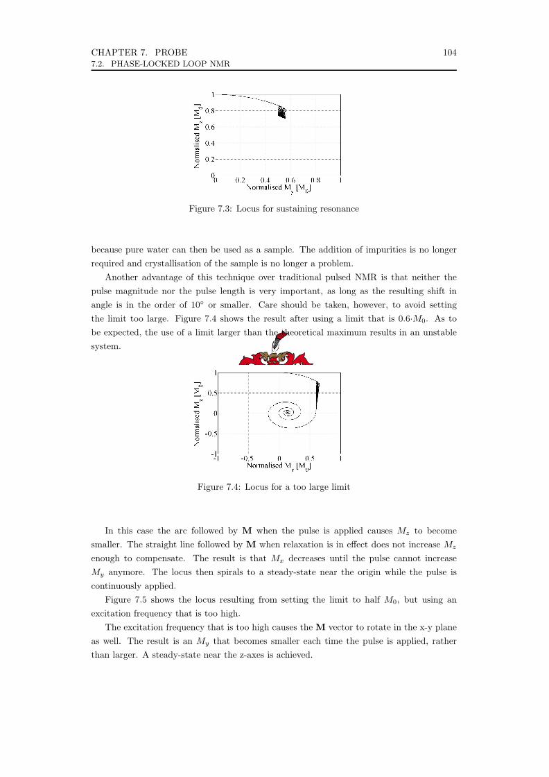
CHAPTER 7. PROBE 1047.2. PHASE-LOCKED LOOP NMR
Figure 7.3: Locus for sustaining resonance
because pure water can then be used as a sample. The addition of impurities is no longerrequired and crystallisation of the sample is no longer a problem.
Another advantage of this technique over traditional pulsed NMR is that neither thepulse magnitude nor the pulse length is very important, as long as the resulting shift inangle is in the order of 10 or smaller. Care should be taken, however, to avoid settingthe limit too large. Figure 7.4 shows the result after using a limit that is 0.6·M0. As tobe expected, the use of a limit larger than the theoretical maximum results in an unstablesystem.
Figure 7.4: Locus for a too large limit
In this case the arc followed by M when the pulse is applied causes Mz to becomesmaller. The straight line followed by M when relaxation is in effect does not increase Mz
enough to compensate. The result is that Mx decreases until the pulse cannot increaseMy anymore. The locus then spirals to a steady-state near the origin while the pulse iscontinuously applied.
Figure 7.5 shows the locus resulting from setting the limit to half M0, but using anexcitation frequency that is too high.
The excitation frequency that is too high causes the M vector to rotate in the x-y planeas well. The result is an My that becomes smaller each time the pulse is applied, ratherthan larger. A steady-state near the z-axes is achieved.
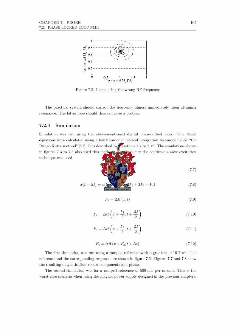
CHAPTER 7. PROBE 1057.2. PHASE-LOCKED LOOP NMR
Figure 7.5: Locus using the wrong RF frequency
The practical system should correct the frequency almost immediately upon attainingresonance. The latter case should thus not pose a problem.
7.2.4 Simulation
Simulation was run using the above-mentioned digital phase-locked loop. The Blochequations were calculated using a fourth-order numerical integration technique called “theRunge-Kutta method” [27]. It is described by equations 7.7 to 7.12. The simulations shownin figures 7.3 to 7.5 also used this method. For simplicity the continuous-wave excitationtechnique was used.
dx
dt= f(x, t) (7.7)
x(t + ∆t) = x(t) +16(F1 + 2F2 + 2F3 + F4) (7.8)
F1 = ∆tf (x, t) (7.9)
F2 = ∆tf(
x +F1
2, t +
∆t
2
)(7.10)
F3 = ∆tf(
x +F2
2, t +
∆t
2
)(7.11)
F4 = ∆tf (x + F3, t + ∆t) (7.12)
The first simulation was run using a ramped reference with a gradient of 10 T·s-1. Thereference and the corresponding response are shown in figure 7.6. Figures 7.7 and 7.8 showthe resulting magnetisation vector components and phase.
The second simulation was for a ramped reference of 500 mT per second. This is theworst-case scenario when using the magnet power supply designed in the previous chapters.

CHAPTER 7. PROBE 1067.2. PHASE-LOCKED LOOP NMR
(a) Reference (b) Response
Figure 7.6: Probe ramp response
(a) x component (b) y component
Figure 7.7: Probe ramp response
(a) z component (b) Phase
Figure 7.8: Probe ramp response
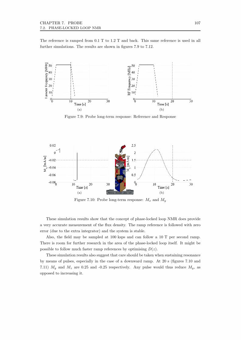
CHAPTER 7. PROBE 1077.2. PHASE-LOCKED LOOP NMR
The reference is ramped from 0.1 T to 1.2 T and back. This same reference is used in allfurther simulations. The results are shown in figures 7.9 to 7.12.
(a) (b)
Figure 7.9: Probe long-term response: Reference and Response
(a) (b)
Figure 7.10: Probe long-term response: Mx and My
These simulation results show that the concept of phase-locked loop NMR does providea very accurate measurement of the flux density. The ramp reference is followed with zeroerror (due to the extra integrator) and the system is stable.
Also, the field may be sampled at 100 ksps and can follow a 10 T per second ramp.There is room for further research in the area of the phase-locked loop itself. It might bepossible to follow much faster ramp references by optimising D(z).
These simulation results also suggest that care should be taken when sustaining resonanceby means of pulses, especially in the case of a downward ramp. At 20 s (figures 7.10 and7.11) My and Mz are 0.25 and -0.25 respectively. Any pulse would thus reduce My, asopposed to increasing it.
CHAPTER 7. PROBE 1087.2. PHASE-LOCKED LOOP NMR
(a) (b)
Figure 7.11: Probe long-term response: Mz and Phase
Figure 7.12: Probe long-term response: Continuous-wave locus
The same simulation was run using 10 µs, 10 µT pulses whenever My is below164 µA·m-1. Each pulse rotates the magnetisation vector through 1.5. The resulting My−z
locus is shown in figure 7.13. The problem is thus solved by using this pulsed technique.
Figure 7.13: Probe long-term response: Pulsed locus
As the frequency increases, so does M0. The result is that the locus rises upwards. Thepulse length is kept constant, resulting in the same angle of rotation of M for each pulse,

CHAPTER 7. PROBE 1097.3. HARDWARE DETAIL
resulting in the larger ‘head’ observed in figure 7.13. As the frequency decreases, the reversepath is followed.
It is also possible to sustain resonance by providing a pulse every time the induced voltage(equation 7.18) drops below some threshold (as apposed to measuring the magnitude of My).The advantage of this is that the receiver circuit can be designed for a very narrow range ofvoltages. Also, analogue comparators can be used instead of ADCs, since the only importantinformation is the zero-crossing (explained in section 7.3.5). Resonance can be maintained bymeans of an analogue circuit, i.e. an envelope detector, comparator, one-shot and analogueswitch. The signal for the analogue switch must also be sent to the FPGA, since no phasemeasurement should be taken while the excitation pulse is present. The fast and expensiveADC is then not necessary. The pin-count of the FPGA also drops. Figure 7.14 shows theresulting locus.
Figure 7.14: Probe long-term response: Modified pulsed locus
The long loop rising to the upper left is due to M0 increasing and therefore also the M
vector. There are no pulses because the frequency rises faster (and therefore the referencefor My drops faster) than My. The same is not true for the return path. It this case, thereference for My rises, causing more frequent pulses in order to keep up. The seemingly flatreference observed in locus to the right is due to a constant frequency. The Mz componentis on its way to a steady state at the bottom right.
During this simulation the fact that Bx is smaller at larger frequencies has been takeninto account, resulting in the smaller changes in the top left-hand region.
7.3 Hardware Detail
7.3.1 Modified Bloch Equations
The flux density within the coil is caused partly by the magnetisation vector and partly bythe magnetic field induced by the coil. By substituting equation 7.13 [5] into the Blochequations (equation C.16 on page 176), equation 7.14 is obtained. It is now possible

CHAPTER 7. PROBE 1107.3. HARDWARE DETAIL
to distinguish between the flux density caused by the excitation signal (µ0H) and themagnetisation vector (µ0M).
B = µ0(H + M) (7.13)
M = γµ0(M×H)−
Mx
T2My
T2Mz−M0
T1
(7.14)
7.3.2 Excitation Coil
It is required that the excitation signal be as large as possible. The buffer that drives thecoil has a maximum voltage of 2Vp−p. The maximum peak voltage over the coil is thus 1 V.The required flux density is in the range of 10 µT (Bx at 5 MHz). Equation 7.17 providesthe number of turns. The factor of two arises from the fact that only half of the actualinduced flux density has an effect on the sample.
N =V
2jωABx(7.15)
The number of turns multiplied by the cross-sectional area must thus be smaller than1.6·10-3 m2. Another consideration is the current in the coil. This is given by equation 7.16.Substituting equation 7.15 yields equation 7.17.
I =V I
jωN2Aµ0(7.16)
lA =V Iµ0
4ωB2x
(7.17)
The AD8062 operational amplifier from Analog Devices provides a bandwidth of300 MHz and a linear output-current of ±25 mA. The volume of the coil must thus beless than 2500 mm3.
7.3.3 Detection Coil
The detected signal voltage is given by equation 7.18. This requires that the NA constantshould be maximised. It is thus chosen to be 1 600 mm2. As seen in figure 7.13, My isalways larger than 164 µA·m-1. The resulting voltage is in the range of 10 µV to 100 µV,depending on the frequency.
V = jωNAµ0Mx−y (7.18)
For good mixing, a signal-strength of between 1 mV and 10 mV is required. This impliesthat a constant gain of 40 dB would be sufficient. RF buffers readily provide a gain of 20 dB.Two of those would thus be enough, one on either side of the cable.

CHAPTER 7. PROBE 1117.3. HARDWARE DETAIL
7.3.4 Using a Single Coil
The two previous sections suggest that the use of a single coil is possible. This has manyadvantages. The first of which is that both the excitation signal and detection signal istaken from the same point. A far more accurate calibration is then possible in order tocompensate for cable-length and circuit delays.
To make the winding of the coil easier, the length must be maximized and the numberof turns minimised. The constants calculated in the previous two sections imply that thereis 1.5 mm per turn, whichever dimensions are chosen. The equations used to calculate theseconstants are only valid for a long coil, however. Inside the probe casing there is space for a30 mm long coil, which is the length chosen. The resulting area is 80 mm2 (10 mm diameter)and the coil must have 20 turns. It is turned using 0.7 mm diameter copper wire, resultingin a series resistance of 30 mΩ, which is acceptable. The capacitance between windings areminimised by evenly spacing each winding 0.7 mm apart. The resulting total capacitance isabout 20 fF. The inductance of the coil is 1.3 µH.
During the detection stage, however, the coil must be seen as an open circuit. Theexcitation signal is large (1 V peak). The AD8062 operational amplifier has an outputswing of 0.3 V to 4.75 V. This implies a peak signal voltage of 2.2 V.
The voltage drop over a diode is typically 0.8 V at 25 mA. Also, the current througha diode is typically 10 pA for the expected 100 µV signal. The equivalent resistances are30 Ω and 10 MΩ respectively. When inserting a diode in series between the driver and thecoil, there is effectively a short circuit from the driver to the coil, but an open circuit fromthe coil to the driver.
7.3.5 Measurement Technique
Different methods are available to measure the magnitude and phase of the NMR signal.The first is to sample the signals directly at the RF frequency. This does not allow for avery accurate phase-measurement. Also, high-speed ADCs are expensive.
The next option would be to mix the detection signal with the excitation signal. Theresult is given by equations 7.19 [1] and 7.20 [27], where y is the result.
y = Arf cos (ωrf t) ·A0 cos (ω0t + φ) (7.19)
y =ArfA0
2cos(φ) +
ArfA0
2cos
((ωrf + ω0)t + φ
)(7.20)
The high-frequency component can be filtered out and the only thing remaining isthe cosine of the phase. The amplitude of the NMR signal can be determined from itsenvelope. One problem is that the phase cannot be measured over the full 360. This isimportant because of the phase shift in the cables and buffers. Although phase at the probeis approximately zero, the phase at the mixers can be any value.
In order to solve this problem, a quadrature mixer may be implemented. The resulting

CHAPTER 7. PROBE 1127.3. HARDWARE DETAIL
equations are 7.21 [1] and 7.22 [27].
y =
Arf cos(ωrf t) ·A0 cos(ω0t + φ)Arf sin(ωrf t) ·A0 sin(ω0t + φ)
(7.21)
y =
Arf A0
2 cos(φ) + Arf A02 cos
((ωrf + ω0)t + φ
)Arf A0
2 sin(−φ) + Arf A02 sin
((ωrf + ω0)t + φ
) (7.22)
The signal that is 90 out of phase can easily be generated using a phase-lockedloop. Also, many ICs are available that offer quadrature demodulation. The two mixedsignals are sampled separately and the phase can be determined over the full 360. Theamplitude measurement is very noisy, however. The calculation of the phase is complicatedto implement within an FPGA.
The final option is to mix both the excitation signal and the detection signal with athird, slightly slower, ‘mixing’ signal [32]. The resulting equations are 7.23 [1] and 7.24 [27].
y =
Amix cos(ωmixt) ·A0 cos(ω0t + φ0)Amix cos(ωmixt) ·Arf cos(ωrf t + φrf )
(7.23)
y =
AmixA0
2 cos((ω0 − ωmix)t + φ0
)+ AmixA0
2 cos((ω0 + ωmix)t + φ0
)AmixArf
2 cos((ωrf − ωmix)t + φrf
)+ AmixArf
2 cos((ωrf + ωmix)t + φrf
) (7.24)
When ωmix is 100 kHz below ωrf , the result is two 100 kHz signals with the same phaserelationship as the original excitation and detection signals. The only disadvantage is thata second DDS is required, but that is outweighed by the accuracy of measurement nowpossible. The probe circuit diagram is presented in figure 7.15.
Chapter 1 – Probe : Hardware Detail 11
The signal that is 90° out of phase can easily be generated using a phase-locked loop. Also, many
ICs are available that offer quadrature demodulation. The two mixed signals are sampled separately
and the phase can be determined over the full 360°. The amplitude measurement is very noisy,
however. The calculation of the phase is also quite complicated to implement within an FPGA.
The final option is to mix both the excitation signal and the detection signal with a third, slightly
slower, ‘mixing’ signal. The resulting equations are 7.23 and 7.24.
( ) ( )( ) ( )
+⋅+⋅
=rfrfrfmixmix
mixmix
tAtAtAtA
φωωφωω
coscoscoscos 000y (1.23)
( )( ) ( )( )
( )( ) ( )( )
++++−
++++−=
rfmixrfrfmix
rfmixrfrfmix
mixmix
mixmix
tAA
tAA
tAAtAA
φωωφωω
φωωφωω
cos2
cos2
cos2
cos2 00
000
0
y (1.24)
When ωmix is 100kHz below ωrf, the result is two 100kHz signals with the same phase relationship
as the original excitation and detection signals. The only disadvantage is that a second DDS is
required, but that is outweighed by the accuracy of measurement now possible. The probe circuit
diagram is presented in figure 7.15.
Probe
DDS1
DDS2
ADC Identical filters
Ω50
Ω50 Ω50
Ω50
Ω50
Ω50Ω50
Figure 1.15 – Probe circuit diagram
The two mixers are implemented with identical Gilbert cell mixers [22] (MC1496). The two
filters are identical 2nd order Butterworth active filters with a cut-off frequency at 150kHz.
The phase is determined from counting the distance between zero-crossings. Care must be taken,
however, in order to ensure that the noise does not cause glitches. A Schmidt-trigger would solve the
problem, but for accurate phase measurement the amplitude of the two signals must then be identical.
This may be achieved by means of a digital normalising algorithm, which would imply that the ADC is
required.
The amplitude of the signal is determined digitally by determining the peak and holding that
value for the duration of the 10µs period. Since the peak is exactly 2.5µs from the positive zero-
Figure 7.15: Probe circuit diagram
The two mixers are implemented with identical Gilbert cell mixers [1] (MC1496). This isa balanced mixer designed for relatively low frequency (<300 MHz) applications. The two
CHAPTER 7. PROBE 1137.3. HARDWARE DETAIL
filters are identical 2nd order Butterworth active filters with a cut-off frequency at 150 kHz.The phase is determined from counting the distance between zero-crossings. Care must
be taken, however, in order to ensure that the noise does not cause glitches. A Schmidt-trigger would solve the problem, but for accurate phase measurement the amplitude of thetwo signals must then be identical. This may be achieved by means of a digital normalisingalgorithm, which would imply that the ADC is required.
The amplitude of the signal is determined digitally by determining the peak and holdingthat value for the duration of the 10 µs period. Since the peak is exactly 2.5 µs fromthe positive zero-crossing, this is easily implemented. When using the comparator option,however, the magnitude must be determined with an analogue circuit. The envelope of theRF-frequency is detected by means of a circuit similar to that in figure 7.16. The operationalamplifier is optional, but does provide a rectifier with zero voltage-drop as well as high inputimpedance.
Chapter 7 – Probe : Hardware Detail 105
crossing, this is easily implemented. When using the comparator option, however, the magnitude must
be determined with an analogue circuit. The envelope of the RF-frequency is detected by means of a
circuit similar to that in figure 7.16. The operational amplifier is optional, but does provide a rectifier
with zero voltage-drop as well as high input impedance.
InOut
Figure 7.16 – Envelope detector
7.2.6 Parasitic Components The only potentially problematic parasitic component is the capacitance of the diodes and
detection buffer. The combined capacitance is in the order of 10pF. The effect is that a current flows
in the coil, which re-induces a magnetic field in the sample. The magnitude of this field is derived in
equations 7.25 to 7.30.
( )yy MHB += 0µ (7.25)
( )yy MHNAv && += 0µ (7.26)
vCi &= (7.27)
( )yy MHNCAi &&&& += 0µ (7.28)
NlH
i y= (7.29)
022
022
µωµω
CANlCANMH yy +
−= (7.30)
The effect is that the magnetisation vector will try to precess about this induced Hy, causing a
phase-shift. In the stationary frame of reference, the induced H follows Mx-y so that they are always
directly opposite each other. The net effect is thus an increase in precessional frequency. The phase-
locked loop will compensate by adjusting the excitation frequency until the equivalent magnetic field
vector (Hz,eq) is exactly opposite the magnetisation vector. This Hz,eq is given by equations 7.31 and
7.32. The resulting error in frequency is thus given by equation 7.33.
0
0, γµ
ωω −= rf
eqzH (7.31)
y
yzeqz M
HMH =, (7.32)
Figure 7.16: Envelope detector
7.3.6 Parasitic Components
The only potentially problematic parasitic component is the capacitance of the diodes anddetection buffer. The combined capacitance is in the order of 10 pF. The effect is that acurrent flows in the coil, which re-induces a magnetic field in the sample. The magnitude ofthis field is derived in equations 7.25 to 7.30.
B = µ0 (Hy + My) (7.25)
v = NAµ0
(Hy + My
)(7.26)
i = Cv (7.27)
i = NCAµ0
(Hy + My
)(7.28)
i =Hyl
N(7.29)
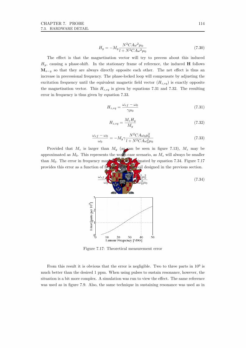
CHAPTER 7. PROBE 1147.3. HARDWARE DETAIL
Hy = −MyN2CAω2µ0
l + N2CAω2µ0(7.30)
The effect is that the magnetisation vector will try to precess about this inducedHy, causing a phase-shift. In the stationary frame of reference, the induced H followsMx−y so that they are always directly opposite each other. The net effect is thus anincrease in precessional frequency. The phase-locked loop will compensate by adjusting theexcitation frequency until the equivalent magnetic field vector (Hz,eq) is exactly oppositethe magnetisation vector. This Hz,eq is given by equations 7.31 and 7.32. The resultingerror in frequency is thus given by equation 7.33.
Hz,eq =ωrf − ω0
γµ0(7.31)
Hz,eq =MzHy
My(7.32)
ωrf − ω0
ω0= −Myγ
N2CAω0µ20
l + N2CAω20µ0
(7.33)
Provided that Mz is larger than My (as can be seen in figure 7.13), Mz may beapproximated as M0. This represents the worst-case scenario, as Mz will always be smallerthan M0. The error in frequency may then be approximated by equation 7.34. Figure 7.17provides this error as a function of frequency for the coil designed in the previous section.
ωrf − ω0
ω0=
a0N2CAω2
0µ20
l + N2CAω20µ0
(7.34)
Figure 7.17: Theoretical measurement error
From this result it is obvious that the error is negligible. Two to three parts in 109 ismuch better than the desired 1 ppm. When using pulses to sustain resonance, however, thesituation is a bit more complex. A simulation was run to view the effect. The same referencewas used as in figure 7.9. Also, the same technique in sustaining resonance was used as in
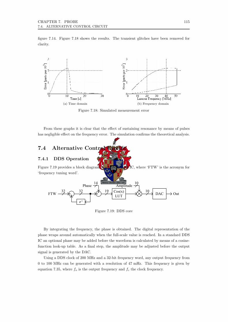
CHAPTER 7. PROBE 1157.4. ALTERNATIVE CONTROL CIRCUIT
figure 7.14. Figure 7.18 shows the results. The transient glitches have been removed forclarity.
(a) Time domain (b) Frequency domain
Figure 7.18: Simulated measurement error
From these graphs it is clear that the effect of sustaining resonance by means of pulseshas negligible effect on the frequency error. The simulation confirms the theoretical analysis.
7.4 Alternative Control Circuit
7.4.1 DDS Operation
Figure 7.19 provides a block diagram of a typical DDS IC, where ‘FTW’ is the acronym for‘frequency tuning word’.
Chapter 7 – Probe : Alternative Control Circuit 107
7.3 Alternative Control Circuit 7.3.1 DDS Operation
Figure 7.19 provides a block diagram of a typical DDS IC, where ‘FTW’ is the acronym for
‘frequency tuning word’.
z-1
Phase Amplitude
OutFTW DACCos(x)LUT
32
14
19
10
1032
Figure 7.19 – DDS core
By integrating the frequency, the phase is obtained. The digital representation of the phase wraps
around automatically when the full-scale value is reached. In a standard DDS IC an optional phase may
be added before the wave-form is calculated by means of a cosine-function look-up table. As a final
step, the amplitude may be adjusted before the output signal is generated by the DAC.
Using a DDS clock of 200MHz and a 32-bit frequency word, any output frequency from 0 to
100MHz can be generated with a resolution of 47mHz. This frequency is given by equation 7.35,
where ‘fo’ is the output frequency and ‘fc’ the clock frequency.
[ ]
( )
−∈
−
∈
=12,2,
21
2,0,2
323132
3132
FTWFTWf
FTWFTWff
c
c
o (7.35)
In the application of the probe, however, the phase and amplitude is not important. Also, the
signal does not need to be sinusoidal. The output may simply be the most significant bit of the phase
accumulator (i.e. digital integrator). Implementation within an FPGA is thus straightforward.
7.3.2 Frequency Content The effect of generating a signal using DDS is to sample the output wave-form at the clock
frequency. This is no problem when generating sinusoidal signals, but the high-frequency harmonics of
the square-wave folds over into the base-band. The frequencies present within the output signal are
given by equation 7.36.
Z∈+= mnmfnff oc , (7.36)
The intended output frequency results when ‘n’ is zero and ‘m’ unity. The largest output
frequency required is 50MHz. Problem areas are where ‘n’ is unity and ‘m’ smaller than 10 and odd.
The ideal situation would thus be to have a clock frequency larger than 500MHz, which is not possible.
The largest practical clock frequency is 320MHz (360MHz for a 24-bit FTW). This would imply that
Figure 7.19: DDS core
By integrating the frequency, the phase is obtained. The digital representation of thephase wraps around automatically when the full-scale value is reached. In a standard DDSIC an optional phase may be added before the waveform is calculated by means of a cosine-function look-up table. As a final step, the amplitude may be adjusted before the outputsignal is generated by the DAC.
Using a DDS clock of 200 MHz and a 32-bit frequency word, any output frequency from0 to 100 MHz can be generated with a resolution of 47 mHz. This frequency is given byequation 7.35, where fo is the output frequency and fc the clock frequency.

CHAPTER 7. PROBE 1167.4. ALTERNATIVE CONTROL CIRCUIT
f0 =
fc
(FTW232
),FTW ∈
[0, 231
]fc
(1− FTW
232
),FTW ∈
(231, 232 − 1
) (7.35)
In the application of the probe, however, the phase and amplitude is not important. Also,the signal does not need to be sinusoidal. The output may simply be the most significantbit of the phase accumulator (i.e. digital integrator). Implementation within an FPGA isthus straightforward.
7.4.2 Frequency Content
The effect of generating a signal using DDS is to sample the output waveform at the clockfrequency. This is no problem when generating sinusoidal signals, but the high-frequencyharmonics of the square wave folds over into the base-band. The frequencies present withinthe output signal are given by equation 7.36.
f = nfc + mf0 |n, m ∈ Z (7.36)
The intended output frequency results when n is zero and m unity. The largest outputfrequency required is 50 MHz. Problem areas are where n is unity and m smaller than 10and odd. The ideal situation would thus be to have a clock frequency larger than 500 MHz,which is not possible. The largest practical clock frequency is 320 MHz (360 MHz for a24-bit FTW). This would imply that there are problem frequencies near 32 MHz, 40 MHzand 53 MHz.
NMR has a very narrow bandwidth and the fundamental signal should have the greatesteffect. A more serious problem arises when mixing all these different frequencies. Thisproblem requires further practical investigation. Possible solutions include sharper filtersand analogue mixers.
When using a square wave to excite the sample, only the first harmonic has any effect.This is due to the very narrow bandwidth of NMR. The magnitude of this first harmonicis 4/π of the magnitude of the square wave. The effective Bx is thus slightly larger using asquare wave than when using a sinusoid of the same amplitude.
7.4.3 Block Diagram
In order to produce a signal that has a zero-average using logic-gates, a differential signal isused. This is then buffered by a differential amplifier before being sent to the probe.
The returning NMR signal is buffered, amplified and conditioned before being sent tothe FPGA. Within the FPGA, XOR gates are used to multiply the mixing signal with theNMR signal. This result is filtered and conditioned outside the FPGA before being fed tothe phase-counter and control circuitry. The resulting block diagram is shown in figure 7.20.
The envelope detector was given in figure 7.16. The differential amplifier circuit diagramis presented in figure 7.21. All resistances are 100 Ω and an AD8062 operational amplifieris used. The output has a peak-to-peak amplitude of 3.3 V and a 2.5 V bias.

CHAPTER 7. PROBE 1177.5. SUMMARY
Chapter 7 – Probe : Alternative Control Circuit 108
there are problem frequencies near 32MHz, 40MHz and 53MHz.
NMR has a very narrow bandwidth and the fundamental signal should have the greatest effect. A
more serious problem arises when mixing all these different frequencies. This problem requires further
practical investigation. Possible solutions include sharper filters and analogue mixers.
When using a square-wave to excite the sample, only the first harmonic has any effect. This is
due to the very narrow bandwidth of NMR. The magnitude of this first harmonic is 4/π of the
magnitude of the square-wave. The effective Bx is thus slightly larger using a square-wave than when
using a sinusoid of the same amplitude.
7.3.3 Block Diagram In order to produce a signal that has a zero-average using logic-gates, a differential signal is used.
This is then buffered by a differential amplifier before sent to the probe.
The returning NMR signal is buffered, amplified and conditioned before being sent to the FPGA.
Within the FPGA, XOR gates are used to multiply the mixing signal with the NMR signal. This result
is filtered and conditioned outside the FPGA before being fed to the phase-counter and control
circuitry. The resulting block diagram is shown in figure 7.20.
Clock EnvelopeDetector
PhaseCounterPLL
DDS1
DDS2
GatingCircuit
FromProbe
ToProbe
Figure 7.20 – Alternative probe control circuit
The envelope detector was given in figure 7.16. The differential amplifier circuit diagram is
presented in figure 7.21. All resistances are 100Ω and an AD8062 operational amplifier is used. The
output has a peak-to-peak amplitude of 3.3V and a 2.5V bias.
Figure 7.20: Alternative probe control circuitChapter 7 – Probe : Summary 109
5V
5V
In Out
Figure 7.21 – Difference amplifier circuit diagram
7.4 Summary This chapter describes the theoretical analysis of a new NMR magnetometer based on a
combination of pulsed and continuous-wave NMR. Resonance is obtained and sustained by providing
short pulses at the Lamour frequency. Each pulse is large enough to keep the system in resonance, but
much smaller than a π/2 pulse. Advantages include smaller pulse-amplifiers and drive circuits.
It is also possible to attain and sustain resonance by means of a very simple analogue circuit.
This circuit comprises of an envelope detector, comparator and one-shot.
The Lamour frequency is tracked by means of a phase-locked loop. Simulation indicated the
validity of this solution. Measurement rate can be increased to 100ksps, which is much faster than
conventional pulsed and continuous-wave NMR magnetometers.
The excitation and detection coil may be the same coil. It has been designed as having a
cylindrical shape. The diameter is 10mm, length 30mm and the coil has 20 turns.
The NMR signal magnitude and phase is measured by mixing both detection and excitation
signals with the same mixing signal. The frequency of the mixing signal is 100kHz below that of the
excitation signal. The amplitude and phase is measured digitally.
The hardware may be simplified by implementing both DDS and mixer circuits within the FPGA.
Numerous advantages have been mentioned, but it does have potential disadvantages as well. These
ideas were not implemented practically but left to future research.
Figure 7.21: Difference amplifier circuit diagram
7.5 Summary
This chapter describes the theoretical analysis of a new NMR magnetometer based on acombination of pulsed and continuous-wave NMR. Resonance is obtained and sustainedby providing short pulses at the Lamour frequency. Each pulse is large enough to keepthe system in resonance, but much smaller than a π/2 pulse. Advantages include smallerpulse-amplifiers and drive circuits.
It is also possible to attain and sustain resonance by means of a very simple analoguecircuit. This circuit comprises of an envelope detector, comparator and one-shot.
The Lamour frequency is tracked by means of a digital phase-locked loop. Simulationindicated the validity of this solution. Measurement rate can be increased to 100 ksps, whichis much faster than conventional pulsed and continuous-wave NMR magnetometers. Also,it is best to use pure water as a sample so that the time-constants T1 and T2 are as large aspossible. This solves the problem of crystallisation.
The excitation and detection coil may be the same coil. It has been designed as having

CHAPTER 7. PROBE 1187.5. SUMMARY
a cylindrical shape. The diameter is 10 mm, length 30 mm and the coil has 20 turns.The NMR signal magnitude and phase is measured by mixing both detection and
excitation signals with the same mixing signal. The frequency of the mixing signal is 100 kHzbelow that of the excitation signal. The amplitude and phase is measured digitally.
The hardware may be simplified by implementing both DDS and mixer circuits within theFPGA. Numerous advantages have been mentioned, but it does have potential disadvantagesas well. These ideas were not implemented practically but left to future research.

Chapter 8
Controller
8.1 Introduction
The previous chapters provided detail on the design of the converter, control system anddigital PWM generator. This chapter describes the design of the controller. The controlleris the central unit from which all other components are controlled.
The hardware is discussed first, followed by the digital circuits within the FPGA. Thedesign and implementation of an embedded processor (a processor implemented within theFPGA) is described in more detail. An FPGA usage summary is also included. For the fulldesign, please refer to appendix D for circuit diagrams and appendix E for VHDL code.
8.2 Hardware
8.2.1 Block Diagram
A detailed block diagram of the controller hardware is presented in figure 8.1.
119

CHAPTER 8. CONTROLLER 1208.2. HARDWARE
Chapter 8 – Controller : Introduction 110
Chapter 8 – Controller
8.0 Introduction The previous chapters provided detail on the design of the converter, control system and digital
PWM generator. This chapter describes the design of the controller. The controller is the central unit
from which all other components are controlled.
The hardware is discussed first, followed by the digital circuits within the FPGA. The design and
implementation of an imbedded processor is described in more detail. An FPGA usage summary is also
included. For the full design, please refer to appendix D for circuit diagrams and appendix E for VHDL
code.
8.1 Hardware 8.1.1 Block Diagram
A detailed block diagram of the controller hardware is presented in figure 8.1.
Voltage RegulatorsExcite
DDS
Mixers ADC1Detect
DAC
ADC2
Line-Driver
Line-Driver
LCDHeader
KeypadHeader
ButtonsHeader
LEDHeader
Central Processor
ProgramHeader
Delay-LinesICs
EEPROM
Programmer
Start-UpCircuit
Power-SupplyHeader
Analogue Meter1-2
Measurement1-4
Switches1-4
RS-232 LCD Keypad Buttons LEDs
Figure 8.1 – Control board block diagram Figure 8.1: Control board block diagram
8.2.2 Central Processor
Any digital circuit requires some form of central processing unit. The main options are touse either a processor (such as a DSP) or programmable logic (such as an FPGA).
A processor has the advantage of containing various useful embedded modules, such asa serial port, timers, etc., implemented and ready to use. One disadvantage, however, isthe difficulty of implementing a fast real time system. Since the program code is evaluatedsequentially, events cannot occur in parallel.
This is where programmable logic takes the lead. Massive parallelisation is possiblewhere, for example, the power supply controller can execute freely from the CPU.Implementing fast real time systems thus becomes possible.
It would also follow logically to use a single processing chip for all the digital tasks. Itis for this reason an FPGA was chosen as the processor of choice. This makes it possibleto implement the interface, peripheral drivers, controller, probe, PWM generator, etc., allwithin the same FPGA. An ALTERA Cyclone II FPGA is used (EP2C8Q208C7).
8.2.3 Power Supply
An ATX power supply switches on when its ‘power-on’ signal is grounded. This is achievedby pressing the ‘on’ button. The power supply responds by bringing all voltages to aregulated state and the asserting the ‘power-good’ signal to 5 V. This latter signal is thenused to drive the gate of a small-signal MOSFET (through a resistor), which then keeps the‘power-on’ signal low. By shorting the gate to ground (i.e. pressing the ‘off’ button), thepower supply is switched off. This circuit is presented in figure 8.2.
When the voltages drift outside the specified range of 5%, the ‘power-good’ signalbecomes low, switching off the MOSFET and thus also switching off the power supply.
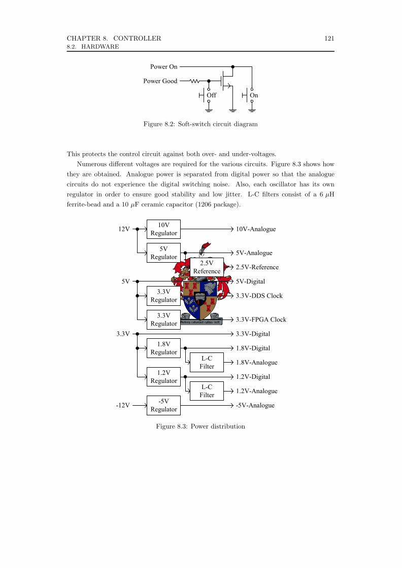
CHAPTER 8. CONTROLLER 1218.2. HARDWARE
Chapter 8 – Controller : Hardware 111
8.1.2 Central Processor Any digital circuit requires some form of central processing unit. The main options are to use
either a processor (such as a DSP) or programmable logic (such as an FPGA).
A processor has the advantage of containing various useful embedded modules, such as a serial
port, timers, etc., implemented and ready to use. One disadvantage, however, is the difficulty of
implementing a fast real-time system. Since the program code is evaluated sequentially, events cannot
occur in parallel.
This is where programmable logic takes the lead. Massive parallelisation is possible where, for
example, the power supply controller can execute quite freely from the CPU. Implementing fast real-
time systems thus becomes possible.
It would also follow logically to use a single processing chip for all the digital tasks. It is for this
reason an FPGA was chosen as the processor of choice. This makes it possible to implement the
interface, peripheral drivers, controller, probe, PWM generator, etc., all within the same FPGA. An
ALTERA Cyclone II FPGA is used (EP2C8Q208C7).
8.1.3 Power Supply An ATX power supply switches on when its ‘power-on’ signal is grounded. This is achieved by
pressing the ‘on’ button. The power-supply responds by bringing all voltages to a regulated state and
the asserting the ‘power-good’ signal high. This latter signal is then used to drive the gate of a small-
signal MOSFET (through a resistor), which then keeps the ‘power-on’ signal low. By shorting the gate
to ground (i.e. pressing the ‘off’ button), the power supply is switched off. This circuit is presented in
figure 8.2.
Power Good
Off On
Power On
Figure 8.2 – Soft-switch circuit diagram
When the voltages drift outside the specified range of 5%, the ‘power-good’ signal becomes low,
switching off the MOSFET and thus also switching off the power supply. This protects the control
circuit against both over- and under-voltages.
Figure 8.2: Soft-switch circuit diagram
This protects the control circuit against both over- and under-voltages.Numerous different voltages are required for the various circuits. Figure 8.3 shows how
they are obtained. Analogue power is separated from digital power so that the analoguecircuits do not experience the digital switching noise. Also, each oscillator has its ownregulator in order to ensure good stability and low jitter. L-C filters consist of a 6 µHferrite-bead and a 10 µF ceramic capacitor (1206 package).
Chapter 8 – Controller : Hardware 112
Numerous different voltages are required for the various circuits. Figure 8.3 shows how they are
obtained. Analogue power is separated from digital power so that the analogue circuits do not
experience the digital switching-noise. Also, each oscillator has its own regulator in order to ensure
good stability and low jitter. L-C filters consist of a 6µH ferrite-bead and a 10µF ceramic capacitor
(1206 package).
10VRegulator12V
5V
3.3V
-12V
5VRegulator
3.3VRegulator
5VRegulator
2.5VReference
3.3VRegulator
1.8VRegulator
L-CFilter
1.2VRegulator
L-CFilter
-5VRegulator
10V-Analogue
5V-Analogue
2.5V-Reference
5V-Digital
3.3V-DDS Clock
3.3V-FPGA Clock
3.3V-Digital
1.8V-Digital
1.8V-Analogue
1.2V-Digital
1.2V-Analogue
-5V-Analogue
Figure 8.3 – Power distribution
8.1.4 Start-Up Sequence FPGA configuration is started by pulsing its ‘n_config’ pin low. This signal is held low for
100ms after the ‘power good’ signal is received from the power supply. Once configuration has
completed successfully, the FPGA asserts the ‘init-done’ pin high.
While this ‘init-done’ is low, the ‘reset’ signal is kept low (as in the case of holding the reset
button down). The reset is released 100ms after the rising edge of the ‘init-done’ signal. This ensures
that all the components within the FPGA are properly reset. A push-button is also provided for system
reset. Figure 8.4 provides a simplified block diagram of the process. Delays are implemented using an
R-C circuit and open-collector comparator.
Figure 8.3: Power distribution
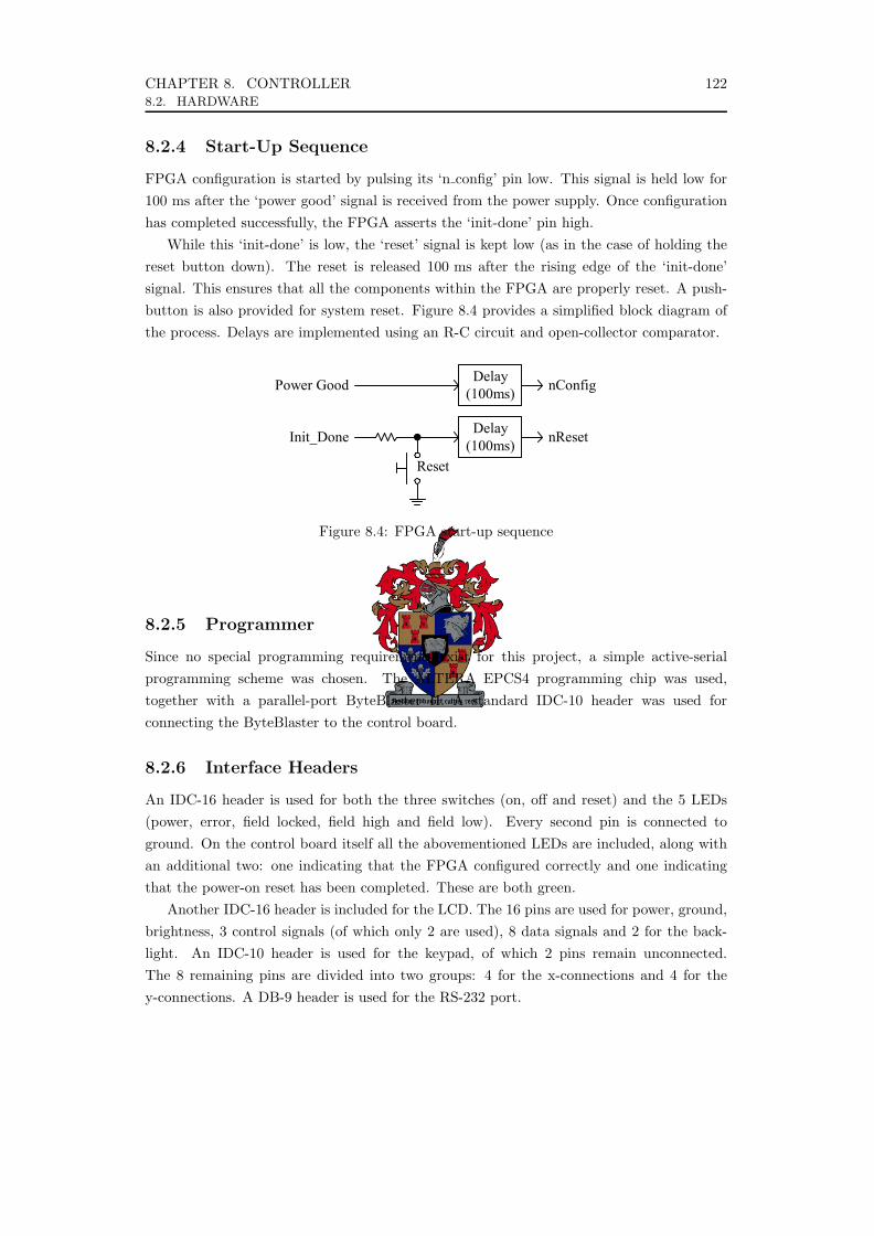
CHAPTER 8. CONTROLLER 1228.2. HARDWARE
8.2.4 Start-Up Sequence
FPGA configuration is started by pulsing its ‘n config’ pin low. This signal is held low for100 ms after the ‘power good’ signal is received from the power supply. Once configurationhas completed successfully, the FPGA asserts the ‘init-done’ pin high.
While this ‘init-done’ is low, the ‘reset’ signal is kept low (as in the case of holding thereset button down). The reset is released 100 ms after the rising edge of the ‘init-done’signal. This ensures that all the components within the FPGA are properly reset. A push-button is also provided for system reset. Figure 8.4 provides a simplified block diagram ofthe process. Delays are implemented using an R-C circuit and open-collector comparator.
Chapter 8 – Controller : Hardware 113
Power Good
Init_Done
Delay(100ms)
Reset
nConfig
Delay(100ms) nReset
Figure 8.4 – FPGA start-up sequence
8.1.5 Programmer Since no special programming requirements exist for this project, a simple active-serial
programming scheme was chosen. The ALTERA EPCS4 programming chip was used, together with a
parallel-port ByteBlaster II. A standard IDC-10 header was used for connecting the ByteBlaster to the
control board.
8.1.6 Interface Headers An IDC-16 header is used for both the three switches (on, off and reset) and the 5 LED’s (power,
error, field locked, field high and field low). Every second pin is connected to ground. On the control
board itself all the abovementioned LED’s are included, along with an additional two: one indicating
that the FPGA configured correctly and one indicating that the power-on reset has been completed.
These are both green.
Another IDC-16 header is included for the LCD. The 16 pins are used for power, ground,
brightness, 3 control signals (of which only 2 are used), 8 data signals and 2 for the back-light. An
IDC-10 header is used for the keypad, of which 2 pins remain unconnected. The 8 remaining pins are
divided into two groups: 4 for the x-connections and 4 for the y-connections. A DB-9 header is used
for the RS-232 port.
8.1.7 ADC Provision is made for four 18-bit measurements from the current source. These are all single-
ended signals in the range of 0 to 5V. The ADC’s, however, require a differential input (each end 0 to
4.096V). First, the incoming signal is scaled down to 0 to 4.096V using a resistor voltage-divider. A
capacitor is included to form a 100kHz, first-order low-pass filter. The scaled signal is then buffered to
produce the positive end of the differential signal. Next, an inverting op-amp amplifier is used to
generate the negative end.
The required sampling frequency is at least once every PWM period, which is 2.620µs. There
must also be enough time left for the control system to work out the next duty-cycle, which is 655ns
(discussed in chapter 5). This leaves 1.965µs for the sampling process to complete. In order for the
Figure 8.4: FPGA start-up sequence
8.2.5 Programmer
Since no special programming requirements exist for this project, a simple active-serialprogramming scheme was chosen. The ALTERA EPCS4 programming chip was used,together with a parallel-port ByteBlaster II. A standard IDC-10 header was used forconnecting the ByteBlaster to the control board.
8.2.6 Interface Headers
An IDC-16 header is used for both the three switches (on, off and reset) and the 5 LEDs(power, error, field locked, field high and field low). Every second pin is connected toground. On the control board itself all the abovementioned LEDs are included, along withan additional two: one indicating that the FPGA configured correctly and one indicatingthat the power-on reset has been completed. These are both green.
Another IDC-16 header is included for the LCD. The 16 pins are used for power, ground,brightness, 3 control signals (of which only 2 are used), 8 data signals and 2 for the back-light. An IDC-10 header is used for the keypad, of which 2 pins remain unconnected.The 8 remaining pins are divided into two groups: 4 for the x-connections and 4 for they-connections. A DB-9 header is used for the RS-232 port.

CHAPTER 8. CONTROLLER 1238.2. HARDWARE
8.2.7 ADC
Provision is made for four 18-bit measurements from the current source. These are all single-ended signals in the range of 0 to 5 V. The ADCs, however, require a differential input (eachend 0 to 4.096 V). First, the incoming signal is scaled down to 0 to 4.096 V using a resistorvoltage-divider. A capacitor is included to form a 100 kHz, first-order low-pass filter. Thescaled signal is then buffered to produce the positive end of the differential signal. Next, aninverting operational amplifier is used to generate the negative end.
The required sampling frequency is at least once every PWM period, which is 2.620 µs.There must also be enough time left for the control system to work out the next duty-cycle,which is 655 ns (discussed in section 5.9.6 on page 88). This leaves 1.965 µs for the samplingprocess to complete. In order for the digital signals to not corrupt the analogue sample,the digital data is read after the conversion is complete. In order to minimise FPGA pinusage, serial-interface ADCs have been chosen. Using a 24 MHz clock to read the 18-bitsample through the serial interface takes 750 ns. This implies a conversion time of at most1.215 µs. The AD7674 from Analog Devices has a conversion time of 1 µs (in ‘warp-mode’)and is thus sufficient.
8.2.8 DAC
An 18-bit, 750 ksps dual DAC (AD1868) is included for the purpose of testing. It is alsoused to drive the analogue meters on the front panel. Its output is in the range of 1.5 Vto 3.5 V. The AD1868 conveniently provides a 2.5 V bias voltage, around which the signalis amplified to have a range 0 V to 5 V. The amplifier is then followed by a second-orderButterworth filter with a cut-off frequency of 325 kHz. This frequency was chosen so thatit is less than half the sample-frequency (Nyquist criterion [29]), and practical componentvalues also played a role. Both amplifiers and filters are implemented using a single quadoperational amplifier (TLE2084).
8.2.9 Gate Signals
It is important to keep the MOSFET gate signals as jitter-free and noise-free as possible. Ahigh-speed logic standard (LVPECL) [33] is thus used for transferring the PWM pulses tothe current source. Single-ended LVPECL has the advantage of using fewer cables, as wellas easier routing. SMA connectors are used with 50 Ω co-axial cable.
To make the LVPECL signals single-ended, the negative signal is terminated on thecontrol board. The driver thus perceives no difference in load. The LVPECL receiver has adifferential-amplifier input. The negative input is connected to the midpoint of the single-ended voltage-swing. The incoming signal is connected to the positive input. This enablesthe receiver to function normally. Figure 8.5 shows the circuit diagram for single-endedLVPECL.
The FPGA has pull-up resistors on its output pins during its configuration stage. In thecase of a half-bridge or synchronous buck converter, this would mean that both MOSFETs

CHAPTER 8. CONTROLLER 1248.2. HARDWARE
Chapter 8 – Controller : Hardware 114
digital signals to not corrupt the analogue sample, the digital data is read after the conversion is
complete. In order to minimise FPGA pin usage, serial-interface ADCs have been chosen. Using a
24MHz clock to read the 18-bit sample through the serial interface takes 750ns. This implies a
conversion-time of at most 1.215us. The AD7674 from Analog Devices has a conversion-time of 1µs
(in ‘warp-mode’) and is thus sufficient.
8.1.8 DAC An 18-bit, 750ksps dual ADC (AD1868) is included for the purpose of testing. It is also used to
drive the analogue meters on the front panel. Its output is in the range of 1.5V to 3.5V. The AD1868
conveniently provides a 2.5V bias voltage, around which the signal is amplified to have a range 0V to
5V. The amplifier is then followed by a second-order Butterworth filter with a cut-off frequency of
325kHz. This frequency has been chosen so that it is less than half the sample-frequency (Nyquist
criterion [24]), and practical component values also played a role. Both amplifiers and filters are
implemented using a single quad op-amp (TLE2084).
8.1.9 Gate Signals It is important to keep the MOSFET gate signals as clean and jitter-free as possible. A high-
speed logic standard (LVPECL) is thus used for transferring the PWM pulses to the current source.
Single-ended LVPECL has the advantage of using fewer cables, as well as easier routing. SMA
connectors are used with 50Ω co-axial cable.
To make the LVPECL signals single-ended, the negative signal is terminated on the control
board. The driver thus perceives no difference in load. The LVPECL receiver has a differential-
amplifier input. The negative input is connected to the midpoint of the single-ended voltage-swing.
The incoming signal is connected to the positive input. This enables the receiver to function normally.
Figure 8.5 shows the circuit diagram for single-ended LVPECL.
82
120
82
120
120
82
3.3V 3.3V 3.3V
Ω50CMOS CMOSLVPECL
Figure 8.5 – Single-ended LVPECL
The FPGA makes its output pins high during its configuration stage. In the case of a half-bridge
or synchronous buck converter, this would mean that both MOSFETs are on, shorting out the bus. A
simple external logic circuit using the four NOR gates in a 74LVC02 IC solves this problem. The
Figure 8.5: Single-ended LVPECL
are on during initialisation, shorting out the bus. A simple external logic circuit using thefour NOR gates in a 74LVC02 IC solves this problem. The schematic is presented in figure8.6. The idea is to let the switching signals through as long as they are not both high atthe same time. When they are high simultaneously, both outputs are low. In the case of astandard buck converter and a full-bridge, this circuit is not required.
Chapter 8 – Controller : Hardware 115
schematic is presented in figure 8.6. The idea is to let the switching signals through as long as they are
not both high at the same time. When they are high simultaneously, both outputs are low. In the case
of a standard buck converter and a full-bridge, this circuit is not required.
S1
S2M2
M1
Figure 8.6 – Failsafe gate signals
8.1.10 Delay Lines In chapter 6 the need for delay lines was discussed. Two delay-lines are included for
experimentation purposes, one for each converter stage.
Since the delay-line functions with LVPECL, the circuit includes a dual CMOS to LVPECL
converter, the two delay-line ICs and a dual LVPECL to CMOS converter.
8.1.11 EEPROM Often the need arises to store data in non-volatile memory. This would include the control-
system parameters, settings prior to power-down, CPU execution code, etc. 64kB of EEPROM is
provided in eight serial-interface 64kb IC’s.
The AT25640 from Atmel has a read cycle as fast as the serial-interface can handle (6.4µs).
Unfortunately, it has a write-cycle of 5ms. Data are usually written sequentially though. Since there
are eight IC’s, the chip address can either be the most-significant three bits of the full 16-bit address, or
the least-significant three. Choosing the least significant three has the advantage that the next byte can
be written while the previous one’s IC is still busy. This means that instead of writing data at a
maximum of 200Bps, data may be written at 1.6kBps. This is advantageous when programming the
CPU.
8.1.12 DDS The DDS IC used for this project (AD9859 from Analog Devices) has a differential current
output. This output needs to be biased externally to 1.8V. Ferrite beads (6µH) are used for this
purpose. Also, a 50Ω output impedance is required in order to match the transmission-line used to send
the signal to the probe. The output current range of each side of the differential output is 0 to 10mA.
The maximum voltage range is 1.8 ± 0.5V. Loading the circuit with a 50Ω resistor would thus meet the
requirements. The circuit is shown in figure 8.7. Capacitances are 100nF.
Figure 8.6: Failsafe gate signals
8.2.10 Delay Lines
In chapter 6 the need for delay lines was discussed. Two delay-lines are included forexperimentation purposes, one for each converter stage.
Since the delay-line functions with LVPECL, the circuit includes a dual CMOS toLVPECL converter, the two delay-line ICs and a dual LVPECL to CMOS converter.
8.2.11 EEPROM
Often the need arises to store data in non-volatile memory. This would include the controlsystem parameters, settings prior to power-down, CPU execution code, etc. 64 kB ofEEPROM is provided in eight serial-interface 64 kb ICs.
The AT25640 from Atmel has a read cycle as fast as the serial-interface can handle(6.4 µs). Unfortunately, it has a write-cycle of 5 ms. Data are usually written sequentially.Since there are eight ICs, the chip address can either be the most-significant three bits ofthe full 16-bit address, or the least-significant three. Choosing the least significant three has

CHAPTER 8. CONTROLLER 1258.2. HARDWARE
the advantage that the next byte can be written while the previous one’s IC is still busy.This means that instead of writing data at a maximum of 200 Bps, data may be written at1.6 kBps. This is advantageous when programming the CPU.
8.2.12 DDS
The DDS IC used for this project (AD9859 from Analog Devices) has a differential currentoutput. This output needs to be biased externally to 1.8 V. Ferrite beads (6 µH) are used forthis purpose. Also, a 50 Ω output impedance is required in order to match the transmissionline used to send the signal to the probe. The output current range of each side of thedifferential output is 0 to 10 mA. The maximum voltage range is 1.8 ± 0.5 V. Loadingthe circuit with a 50 Ω resistor would thus meet the requirements. The circuit is shown infigure 8.7. Capacitances are 100 nF.
Chapter 8 – Controller : Hardware 116
1.8V 1.8V
OutΩ50
Figure 8.7 – DDS biasing circuit
This circuit may be simplified to the circuit in figure 8.8, which removes the need for ferrite-
beads. The output of the DDS IC is then at its limit, which is not a good situation. The circuit above
was used instead. Another advantage of the above circuit is that the ferrite beads isolate the analogue
output from any digital transient voltage disturbances that might be present on the 1.8V supply.
1.8V OutΩ50
Figure 8.8 – Simplified DDS biasing circuit
Figure 8.7: DDS biasing circuit
This circuit may be simplified to the circuit in figure 8.8, which removes the need forferrite-beads. The output of the DDS IC is then at its limit, which is not a good situation.The circuit above was used instead. Another advantage of the above circuit is that theferrite beads isolate the analogue output from any digital transient voltage disturbancesthat might be present on the 1.8 V supply.
Chapter 8 – Controller : Hardware 116
1.8V 1.8V
OutΩ50
Figure 8.7 – DDS biasing circuit
This circuit may be simplified to the circuit in figure 8.8, which removes the need for ferrite-
beads. The output of the DDS IC is then at its limit, which is not a good situation. The circuit above
was used instead. Another advantage of the above circuit is that the ferrite beads isolate the analogue
output from any digital transient voltage disturbances that might be present on the 1.8V supply.
1.8V OutΩ50
Figure 8.8 – Simplified DDS biasing circuit Figure 8.8: Simplified DDS biasing circuit

CHAPTER 8. CONTROLLER 1268.2. HARDWARE
8.2.13 Mixer
A Gilbert cell mixer [1] is shown in figure 8.9, along with the biasing used in the probecircuit. The MC1496 from ON Semiconductor was used.
Chapter 8 – Controller : Hardware 117
8.1.13 Mixer A Gilbert cell mixer [22] is shown in figure 8.9, along with the biasing used in the probe circuit.
The MC1496 from ON Semiconductor was used.
100n
10V
10V10V 10V
100Ω 100n
100Ω
1kΩ
22kΩ
500Ω500Ω
22kΩ5.6kΩ 5.6kΩ
500Ω
10kΩ
10kΩMixing signal
Input
Output
Figure 8.9 – Gilbert cell mixer
The basic operation is based on the fact that the gain of a common-emitter transistor amplifier is
directly proportional to its biasing current [18]. The bottom pair alters the biasing currents of the top
two pairs, thus altering their gain. The result is the product of the two input signals.
8.1.14 Transmission-Lines Both switching signals and probe signals are high-frequency signals that need to travel over
extended distances. Transmission lines are thus needed on the PCB so that the connections to the co-
axial lines are impedance-matched. Figure 8.10 shows the cross-section of a strip-line transmission
line.
Copper
PCB Materiald
tw
Signal
Ground Figure 8.10 – Strip-line transmission line
Figure 8.9: Gilbert cell mixer [1]
The basic operation is based on the fact that the gain of a common-emitter transistoramplifier is directly proportional to its biasing current [34]. The bottom pair alters thebiasing currents of the top two pairs, thus altering their gain. The result is the product ofthe two input signals.
8.2.14 Transmission Lines
Both switching signals and probe signals are high-frequency signals that need to travel overextended distances. Transmission lines are thus needed on the PCB so that the connectionsto the co-axial lines are impedance-matched. Figure 8.10 shows the cross-section of a strip-line transmission line.
The equation for the characteristic impedance of this line is giving by equation 8.1 [35],where εr is the relative permittivity of the PCB material.
Z0 =87√
εr + 1.41ln
(5.98d
0.8w + t
)Ω (8.1)
For a standard 1.55 mm 4-layer or 6-layer PCB, t is 15 µm, d 238 µm and εr 4.6. Thisimplies a width of 416 µm. Similarly, for a 1.55 mm double-layer PCB, d is 1.5 mm and therequired width is 2.72 mm.

CHAPTER 8. CONTROLLER 1278.2. HARDWARE
Chapter 8 – Controller : Hardware 117
8.1.13 Mixer A Gilbert cell mixer [22] is shown in figure 8.9, along with the biasing used in the probe circuit.
The MC1496 from ON Semiconductor was used.
100n
10V
10V10V 10V
100Ω 100n
100Ω
1kΩ
22kΩ
500Ω500Ω
22kΩ5.6kΩ 5.6kΩ
500Ω
10kΩ
10kΩMixing signal
Input
Output
Figure 8.9 – Gilbert cell mixer
The basic operation is based on the fact that the gain of a common-emitter transistor amplifier is
directly proportional to its biasing current [18]. The bottom pair alters the biasing currents of the top
two pairs, thus altering their gain. The result is the product of the two input signals.
8.1.14 Transmission-Lines Both switching signals and probe signals are high-frequency signals that need to travel over
extended distances. Transmission lines are thus needed on the PCB so that the connections to the co-
axial lines are impedance-matched. Figure 8.10 shows the cross-section of a strip-line transmission
line.
Copper
PCB Materiald
tw
Signal
Ground Figure 8.10 – Strip-line transmission line Figure 8.10: Strip-line transmission line
8.2.15 FPGA I/O Pin-Count
Conveniently, many components share the same signal, thus decreasing the FPGA I/O pin-count. These signals include data lines, clocks, etc. The full I/O pin-count is presented intable 8-I.
Table 8-I: FPGA I/O pin-count
Peripheral Component Pins
Power and start-up Power-good signal 1
Interface Reset switch 1
LEDs 6
LCD 11
Keypad 8
RS-232 2
Probe DDS (x2) 5
ADC 9
ADC ADC (x4) 11
DAC DAC 4
Switches Switches 4
Delay lines Delay lines (x2) 24
EEPROM EEPROM (x8) 11
Clock 125 MHz oscillator 1
Total 98
Many components listed in this table are for experimentation purposes only. The pin-count of the final product will be much lower and a smaller FPGA may thus be used.
8.2.16 Physical Layout
The control board PCB consists of four layers. These are, from top to bottom:
• Top signal and transmission lines
• Ground (single solid plane)
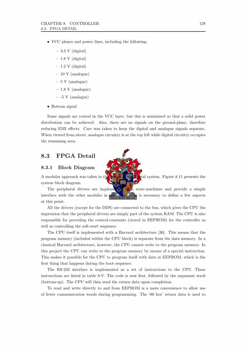
CHAPTER 8. CONTROLLER 1288.3. FPGA DETAIL
• VCC planes and power lines, including the following:
– 3.3 V (digital)
– 1.8 V (digital)
– 1.2 V (digital)
– 10 V (analogue)
– 5 V (analogue)
– 1.8 V (analogue)
– -5 V (analogue)
• Bottom signal
Some signals are routed in the VCC layer, but this is minimised so that a solid powerdistribution can be achieved. Also, there are no signals on the ground-plane, thereforereducing EMI effects. Care was taken to keep the digital and analogue signals separate.When viewed from above, analogue circuitry is at the top left while digital circuitry occupiesthe remaining area.
8.3 FPGA Detail
8.3.1 Block Diagram
A modular approach was taken in the design of the digital system. Figure 8.11 presents thesystem block diagram.
The peripheral drivers are implemented with state-machines and provide a simpleinterface with the other modules in the system. It is necessary to define a few aspectsat this point.
All the drivers (except for the DDS) are connected to the bus, which gives the CPU theimpression that the peripheral drivers are simply part of the system RAM. The CPU is alsoresponsible for providing the control-constants (stored in EEPROM) for the controller aswell as controlling the soft-start sequence.
The CPU itself is implemented with a Harvard architecture [36]. This means that theprogram memory (included within the CPU block) is separate from the data memory. In aclassical Harvard architecture, however, the CPU cannot write to the program memory. Inthis project the CPU can write to the program memory by means of a special instruction.This makes it possible for the CPU to program itself with data in EEPROM, which is thefirst thing that happens during the boot sequence.
The RS-232 interface is implemented as a set of instructions to the CPU. Theseinstructions are listed in table 8-V. The code is sent first, followed by the argument stack(bottom-up). The CPU will then send the return data upon completion.
To read and write directly to and from EEPROM is a mere convenience to allow useof fewer communication words during programming. The ‘00 hex’ return data is used to

CHAPTER 8. CONTROLLER 1298.3. FPGA DETAIL
Chapter 8 – Controller : FPGA Detail 120
8.2 FPGA Detail 8.2.1 Block Diagram
A modular approach was taken in the design of the digital system. Figure 8.11 presents the
system block-diagram.
DDS
ADC1
DDSDriver
ADC1Driver
Probe
Power Good
ADC2Driver
Reset Global
PLL
ClockGenerator
Controller
ADC2
Clock
195.3125MHz98MHz49MHz24MHz6MHz1.5MHz5.960kHz Global
GlobalGlobalGlobalGlobalGlobal
CPUBus
RAM
EEPROMRS-232Keypad
LCDLED
DACEEPROMRS-232KeypadLCDLED
AddressData
(125MHz)
DAC
PWM1Delay-Line1Switches1-2
PWM2Delay-Line2Switches3-4
Figure 8.11 – FPGA block diagram
The peripheral drivers are implemented with state-machines and provide a simple interface with
the other modules in the system. Although these interfaces and detail of operation are fully included in
chapter 11, it is necessary to define a few aspects at this point.
All the drivers (except for the DDS) are connected to the bus, which gives the CPU the
impression that the peripheral drivers are simply part of the system RAM. The CPU is also responsible
for providing the control-constants (stored in EEPROM) for the controller as well as controlling the
soft-start sequence.
The CPU itself is implemented with a Harvard architecture [33]. This means that the program
memory (included within the CPU block) is separate from the data memory. In a classical Harvard
architecture, however, the CPU cannot write to the program memory. In this project the CPU can write
to the program memory by means of a special instruction. This makes it possible for the CPU to
program itself with data in EEPROM, which is the first thing that happens during the boot sequence.
The RS-232 interface is implemented as a set of instructions to the CPU. These instructions are
listed in table 8-II. The code is sent first, followed by the argument stack (bottom-up). The CPU will
Figure 8.11: FPGA block diagram
signal that the next EEPROM ‘write’ instruction may be given. This is included becausethe EEPROM write-cycle is much slower than the time it takes for the instruction to besent via 115200 baud RS-232.
As the CPU perceives all the peripherals as RAM, reading and writing to and from RAMenables the computer to fully control the system if desired.
8.3.2 Clock Requirements and Generation
Table 8-II shows the components implemented within the FPGA, along with their clockrequirements. These are calculated using timing requirements of the components, such asmaximum SPI clock frequency. Since the component clock is generated using state-machines,the required frequency is doubled.
The only component that needs an exact clock is the PWM, since its period needs tobe an exact integer multiple of the delay-line resolution (10 ps). A 125 MHz oscillator IC isused as a master clock for the FPGA. The internal phase-locked loop is then used to dividethis frequency by 16 and multiply the result by 25. This provides a clock of 195.3125 MHz,which is exactly double the desired PWM clock frequency.
This 195 MHz signal is used to clock a 15-bit synchronous up-counter in order to generatethe various in-phase harmonic clocks needed by the system. Also included in table 8-II isthe counter tap (equivalent to the power of 2 by which the 195 MHz signal is divided) andthe actual clock used in the design.

CHAPTER 8. CONTROLLER 1308.4. PERIPHERAL SOFTWARE
Table 8-II: FPGA clock requirements
Component Clock requirement Counter tap Actual Clk
[Hz] [Hz]
ADC (Probe) < 60 000 000 2 48 828 125.000
ADC (Controller) < 80 000 000 2 48 828 125.000
COMM >> 115 200 5 6 103 515.625
Controller ≈ 50 000 000 2 48 828 125.000
Controller : ∆t ≈ 4 000 15 5 960.464
CPU ≈ 1 000 000 7 1 525 878.906
DAC < 27 000 000 3 24 414 062.500
DDS < 50 000 000 2 48 828 125.000
EEPROM < 10 000 000 5 6 103 515.625
Keypad ≈ 4 000 15 5 960.464
LCD < 4 000 000 7 1 525 878.906
PWM = 97 656 250 1 97 656 250.000
8.4 Peripheral Software
8.4.1 EEPROM
Each EEPROM IC has four control lines. These are ‘data in’, ‘data out’, ‘data clock’ and‘chip-select’. The data lines are shared between the eight ICs, implying a total of 11 lines.
After reset, each IC is initialised. This is performed by reading the status register of eachand determining whether or not it is set up correctly. If not, the problem is corrected. Thestatus register is non-volatile, so a write operation will only occur upon the first power-upof the controller.
Before each interaction with a particular IC, the ‘Busy’ bit in the status register is read.The controller waits for that particular IC to finish before sending the relevant instruction.
In order to speed up the writing process, the least significant 3 bits of the 16-bit addressare used to decode the chip-select signal. The result is that the next byte in the stream maybe written while the previous seven ICs are still busy.
On the CPU side, the data and address are set up before an instruction is provided. Oncethe instruction is given, the I/O registers become read-only until the operation is complete.Figure 8.12 provides a flow-diagram.
The address allocation table is presented in table 8-III.Much space remains available between addresses ‘4000’ and ‘8000’ to store data needed
for future developments. Such developments might include data redundancy so that no dataloss occurs during a power-failure.

CHAPTER 8. CONTROLLER 1318.4. PERIPHERAL SOFTWARE
Chapter 8 – Controller : Peripheral Software 123
Status = "10"?(Read)
Initialise
Reset
Status = "01"?(Write)
Select IC andMake registers read-only
Select IC andMake registers read-only
IC Busy?
IC Busy?
Read Data
Write Data
Set Status = "00" andMake registers writable
N
Y
YN
Y
Y
N
N
Figure 8.12 – EEPROM driver flow diagram Figure 8.12: EEPROM driver flow diagram
Table 8-III: EEPROM address allocations
Group Data Start address End address
Program Execution code 0000 1FFF
Menus Menu text 8000 FFFF
Stage 1 controller V1 gain 2000 2002
I1 gain 2004 2006
Reference gain 2008 200A
Reference ramp limiter 200C 200E
Stage 2 controller V2 gain 2010 2012
I2 gain 2014 2016
I3 gain 2018 201A
Integrator gain 201C 201E
Reference gain 2020 2022
Reference ramp limiter 2024 2026
Controller Status 2027 2027
Reference 2028 202B
Probe Field constant 2FFC 2FFF
Phase compensation LUT 3000 3FFF

CHAPTER 8. CONTROLLER 1328.4. PERIPHERAL SOFTWARE
8.4.2 LCD
The LCD driver is very simple. Once the LCD has been initialised after reset, the LCDbuffer (RAM) is continuously copied to the LCD. It takes 4.2 ms to copy the 80 charactersand as such the LCD is updated at a frequency of 238 Hz. This is much faster than can beperceived by the human eye.
All the CPU sees is a RAM block of 128 bytes. It can read and write to this block. Themost significant 2 bits of the 7-bit address represents the line and the least significant 5 bitsthe character within that line.
8.4.3 Keypad
The keypad driver consists of two parts: a keypad reader and a FIFO queue. Figure8.13 shows the connections within a keypad. By pressing a button the two lines crossingunderneath are connected.
Chapter 8 – Controller : Peripheral Software 125
y11 2 3 A
4 5 6 B
7 8 9 C
* 0 # D
y2
y3
y4
x1 x2 x3 x4 Figure 8.13 – Keypad connections
The keypad reader alternately drives each of the four y-connections high while keeping the other
three at high-impedance. The x-connections are then read at each point to map the status of the 16
buttons. When the button is not pushed, its corresponding x-connection is pulled low by means of a
10kΩ resistor. In order to lower sensitivity to glitches, the past 5 samples must be the same before the
status changes.
When a button has been pushed and the status updated, the event is stored in a circular FIFO
queue of length eight. When two buttons are pressed at once, the event is ignored. The button must be
released before another event can be registered.
The CPU reads the data from the keypad driver to determine whether a key has been pressed.
The least significant 4 bits represent the key code (table 8-V). The most significant (8th) bit is high
when the queue is empty. By writing to the keypad driver the data output is updated with the next item
in the queue.
Figure 8.13: Keypad connections
The keypad reader alternately drives each of the four y-connections high while keepingthe other three at high-impedance. The x-connections are then read at each point to mapthe status of the 16 buttons. When the button is not pushed, its corresponding x-connectionis pulled low by means of a 10 kΩ resistor. In order to lower sensitivity to glitches, the past5 samples must be the same before the status changes.
When a button has been pushed and the status updated, the event is stored in a circularFIFO queue of length eight. When two buttons are pressed at once, the event is ignored.The button must be released before another event can be registered.
The CPU reads the data from the keypad driver to determine whether a key has beenpressed. The least significant 4 bits represent the key code (table 8-IV). The most significant(8th) bit is high when the queue is empty. By writing to the keypad driver the data outputis updated with the next item in the queue.

CHAPTER 8. CONTROLLER 1338.4. PERIPHERAL SOFTWARE
Table 8-IV: Key codes
Code Key
0000 0
0001 1
0010 2
0011 3
0100 4
0101 5
0110 6
0111 7
1000 8
1001 9
1010 A
1011 B
1100 C
1101 D
1110 *
1111 #
8.4.4 ADC
The ADC conversion cycle is started by pulsing the ‘conversion-start’ signal low. The ADCthen responds by making its ‘busy’ signal high.
In order to synchronise the four ADCs, their ‘conversion start’ signals are all connectedtogether. Their ‘data’ and ‘busy’ signals are kept separate in order to allow all four to beread at the same time. The read cycle is started once all four ‘busy’ signals become low.
8.4.5 DAC
The DAC driver works similarly to that of the LCD. The CPU can read and write to theDAC buffer. The DAC driver continuously updates the DAC IC at a rate of 650 ksps.
The driver also automatically converts the absolute value given by the CPU to a two’scomplement representation accepted by the DAC. The most significant bit of the data isinverted while all the others are not.
Each channel of the dual DAC is followed by a 2nd order Butterworth low-pass activefilter with a cut-off frequency at 325 kHz.
8.4.6 RS-232
The fastest reliable RS-232 connection was found to be 115200 baud. A 6 MHz clock is usedto calculate the necessary delays.
The RS-232 driver has three modules. These are a sender, receiver and controller. Thesender retains a high output until it is required to send, or for a minimum of 8.68 µs. This

CHAPTER 8. CONTROLLER 1348.4. PERIPHERAL SOFTWARE
represents the ‘stop bit’. The data is preceded by a ‘start bit’ (output low) before beingsent. It is sent, least significant bit first, at one bit every 8.68 µs.
The receiver waits for a falling edge (‘start bit’), after which it pauses for 13.0 µs (oneand a half bits). It then loads the data (least significant bit first) once every 8.68 µs. Thisensures that the data is sampled in the middle of the bit, rather than near an edge.
The controller provides an interface to the CPU. The transmit data register can be readand written. The received data register is read-only. The status register has two bits, a‘send’ bit and ‘received’ bit. The CPU can set the ‘send’ bit, but not clear it. Similarly,the ‘received bit’ can be cleared, but not set. Thus writing ‘11’ to the status register startstransmitting data without influencing the status of the receiver. Similarly, writing ‘00’ tothe status register acknowledges that the received data has been read without influencingthe status of the transmitter. The controller resets the ‘send’ bit upon completion and setsthe ‘received’ bit upon receiving data.
Although not yet implemented, it is intended for the RS-232 to have a FIFO queue [37](for received data) 512 bytes long (1 M4K block). There is no ‘send’ buffer and the CPUmust wait for the one byte to finish sending before it can send the next. No RS-232 commandrequires more than one byte return data, so this is not a problem. Table 8-V presents thecommands.
Table 8-V: RS-232 Instructions
Operation Code Argument stack Return data
No operation 0x00 Empty None
Write EEPROM 0x01 Data 0x00
Address1
Address0
Read EEPROM 0x02 Address1 Data
Address0
Reboot 0x03 Empty None
Write RAM 0x04 Data None
Address1
Address0
Read RAM 0x05 Address1 Data
Address0
Any of the CPU functions can be controlled by manipulating the RAM. It is for thisreason there are so few instructions. The ability to manipulate the EEPROM directly issimply to decrease the time it takes to read or write large amounts of data via the relativelyslow serial connection.

CHAPTER 8. CONTROLLER 1358.4. PERIPHERAL SOFTWARE
8.4.7 Bus
The purpose of the bus module is to map all the different components to a RAM addressspace. It achieves this by decoding the address and then connecting the correct data portand latch to the CPU data port and latch. The assigned addresses are presented in table8-VI.
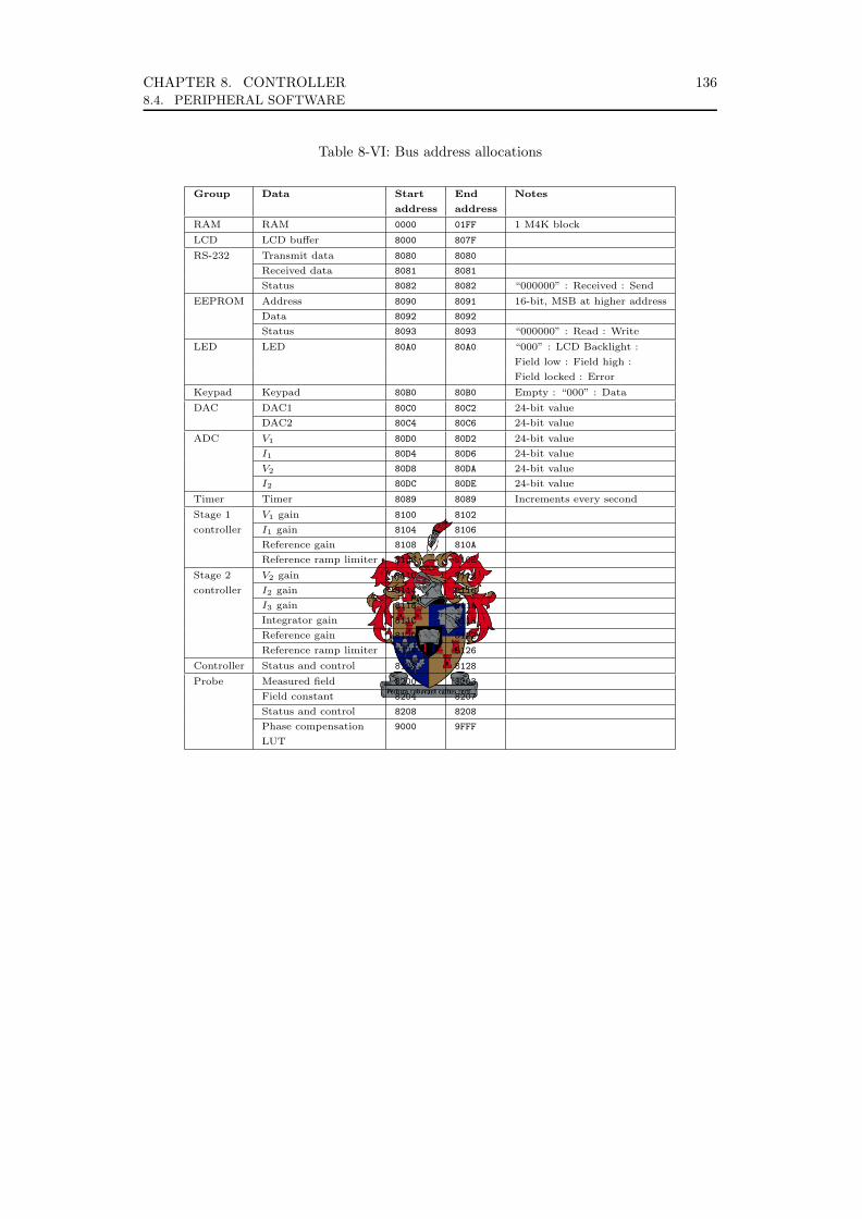
CHAPTER 8. CONTROLLER 1368.4. PERIPHERAL SOFTWARE
Table 8-VI: Bus address allocations
Group Data Start End Notes
address address
RAM RAM 0000 01FF 1 M4K block
LCD LCD buffer 8000 807F
RS-232 Transmit data 8080 8080
Received data 8081 8081
Status 8082 8082 “000000” : Received : Send
EEPROM Address 8090 8091 16-bit, MSB at higher address
Data 8092 8092
Status 8093 8093 “000000” : Read : Write
LED LED 80A0 80A0 “000” : LCD Backlight :
Field low : Field high :
Field locked : Error
Keypad Keypad 80B0 80B0 Empty : “000” : Data
DAC DAC1 80C0 80C2 24-bit value
DAC2 80C4 80C6 24-bit value
ADC V1 80D0 80D2 24-bit value
I1 80D4 80D6 24-bit value
V2 80D8 80DA 24-bit value
I2 80DC 80DE 24-bit value
Timer Timer 8089 8089 Increments every second
Stage 1 V1 gain 8100 8102
controller I1 gain 8104 8106
Reference gain 8108 810A
Reference ramp limiter 810C 810E
Stage 2 V2 gain 8110 8112
controller I2 gain 8114 8116
I3 gain 8118 811A
Integrator gain 811C 811E
Reference gain 8120 8122
Reference ramp limiter 8124 8126
Controller Status and control 8128 8128
Probe Measured field 8200 8203
Field constant 8204 8207
Status and control 8208 8208
Phase compensation 9000 9FFF
LUT

CHAPTER 8. CONTROLLER 1378.5. CPU
8.5 CPU
8.5.1 Justification
There are three options available when implementing a large interface. The first is to usea very large state-machine, which occupies much valuable space within the FPGA. Thesecond is to use an embedded processor, which is basically a much smaller, but generalpurpose state-machine. The third option is to use an external processor, such as a ‘PIC’from Microchip.
Altera offers an embedded processor called ‘Nios’, which can be customised to the specificapplication and programmed using the C programming language. This saves developmenttime on a complex processor, but is very expensive intellectual property. The externalprocessor is a very attractive option, since it has a built-in RS-232 and USB interface.
The 16 lines needed for the bus can easily be implemented with a standard 4-port PIC. Italso provides more program memory than is available on the FPGA. A minor disadvantageis the fact that it uses space on the controller PCB and valuable I/O pins. The next iterationof the design must consider this option.
The controller board that was built, however, does not include an external processor.Since this project requires a very simple processor with little functionality, a new embeddedprocessor was developed. The total development time was two weeks, including writing anassembler, programmer and boot loader.
8.5.2 Block Diagram
A Harvard architecture is used, where the program memory is separate from data memory.This is to simplify the instruction fetch stage. Both program memory and data memorymay be manipulated. A 16-bit address space is used for both. Also, the essence of operationis a simple stack machine. The block diagram of the processor is presented in figure 8.14.A description of each signal path follows in table 8-VII.

CHAPTER 8. CONTROLLER 1388.5. CPU
Chapter 8 – Controller : CPU 131
Core
Multiplier
ProgramStack
Bus
ProgramMemory
ArithmeticStack
ArithmeticUnit
A B C
D
E
FGHI
J
K
L
Figure 8.14 – CPU block diagram Figure 8.14: CPU block diagram
It must be noted that both the arithmetic stack and the program stack do not provideany indication of when they are full. Both are implemented as circular lists and will neveroverflow. The program and arithmetic stacks have lengths of 256 and 8 respectively. It isleft to the programmer to ensure that the data stored within is not overwritten withoutintention.
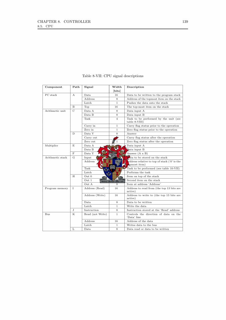
CHAPTER 8. CONTROLLER 1398.5. CPU
Table 8-VII: CPU signal descriptions
Component Path Signal Width Description
[bits]
PC stack A Data 16 Data to be written to the program stack
Address 8 Address of the topmost item on the stack
Latch 1 Pushes the data onto the stack
B Top 16 The top-most item on the stack
Arithmetic unit C Data A 8 Data input A
Data B 8 Data input B
Task 4 Task to be performed by the unit (seetable 8-VIII)
Carry in 1 Carry flag status prior to the operation
Zero in 1 Zero flag status prior to the operation
D Data Y 8 Answer
Carry out 1 Carry flag status after the operation
Zero out 1 Zero flag status after the operation
Multiplier E Data A 8 Data input A
Data B 8 Data input B
F Data Y 16 Answer (A x B)
Arithmetic stack G Input 8 Data to be stored on the stack
Address 3 Address relative to top of stack (‘0’ is thetopmost item)
Task 2 Task to be performed (see table 10-VII)
Latch 1 Performs the task
H Out 0 8 Item on top of the stack
Out 1 8 Second item on the stack
Out A 8 Item at address ‘Address’
Program memory I Address (Read) 16 Address to read from (the top 13 bits areactive)
Address (Write) 16 Address to write to (the top 13 bits areactive)
Data 8 Data to be written
Latch 1 Write the data
J Instruction 8 Instruction stored at the ‘Read’ address
Bus K Read (not Write) 1 Controls the direction of data on the‘Data’ line
Address 16 Address of the data
Latch 1 Writes data to the bus
L Data 8 Data read or data to be written
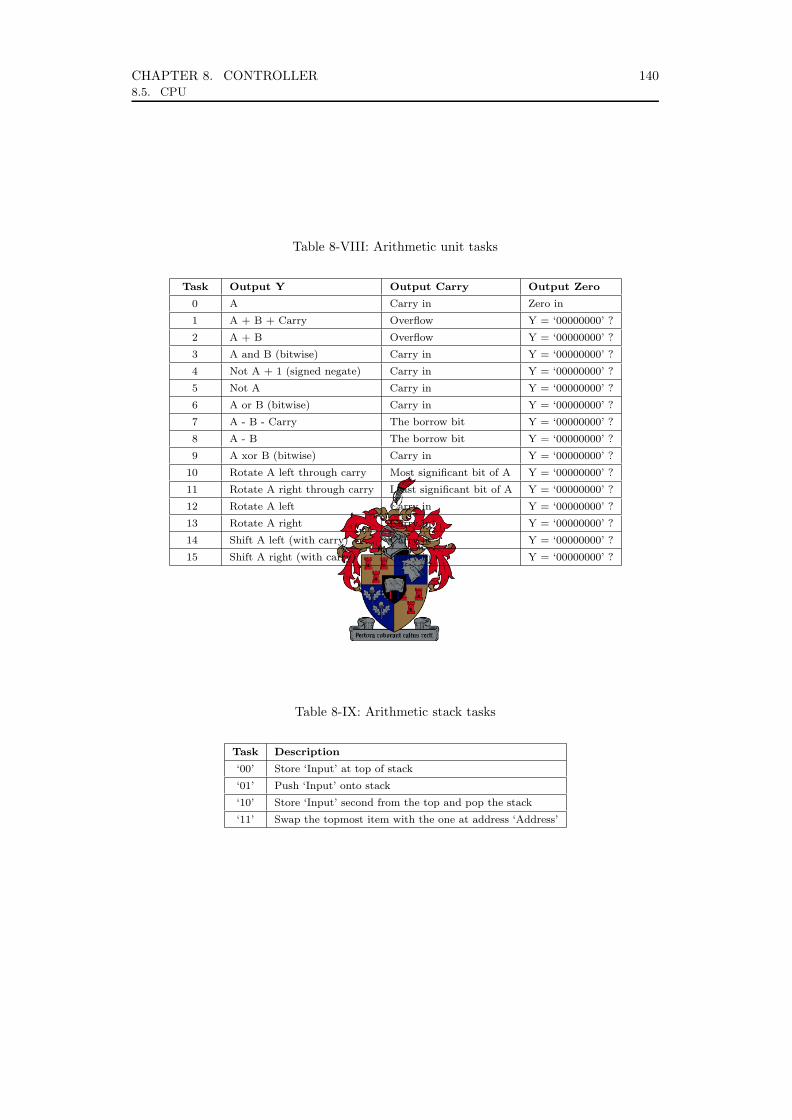
CHAPTER 8. CONTROLLER 1408.5. CPU
Table 8-VIII: Arithmetic unit tasks
Task Output Y Output Carry Output Zero
0 A Carry in Zero in
1 A + B + Carry Overflow Y = ‘00000000’ ?
2 A + B Overflow Y = ‘00000000’ ?
3 A and B (bitwise) Carry in Y = ‘00000000’ ?
4 Not A + 1 (signed negate) Carry in Y = ‘00000000’ ?
5 Not A Carry in Y = ‘00000000’ ?
6 A or B (bitwise) Carry in Y = ‘00000000’ ?
7 A - B - Carry The borrow bit Y = ‘00000000’ ?
8 A - B The borrow bit Y = ‘00000000’ ?
9 A xor B (bitwise) Carry in Y = ‘00000000’ ?
10 Rotate A left through carry Most significant bit of A Y = ‘00000000’ ?
11 Rotate A right through carry Least significant bit of A Y = ‘00000000’ ?
12 Rotate A left Carry in Y = ‘00000000’ ?
13 Rotate A right Carry in Y = ‘00000000’ ?
14 Shift A left (with carry) Carry in Y = ‘00000000’ ?
15 Shift A right (with carry) Carry in Y = ‘00000000’ ?
Table 8-IX: Arithmetic stack tasks
Task Description
‘00’ Store ‘Input’ at top of stack
‘01’ Push ‘Input’ onto stack
‘10’ Store ‘Input’ second from the top and pop the stack
‘11’ Swap the topmost item with the one at address ‘Address’
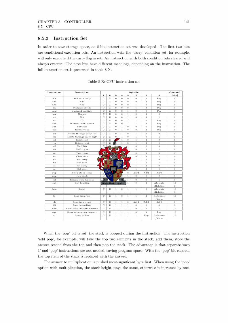
CHAPTER 8. CONTROLLER 1418.5. CPU
8.5.3 Instruction Set
In order to save storage space, an 8-bit instruction set was developed. The first two bitsare conditional execution bits. An instruction with the ‘carry’ condition set, for example,will only execute if the carry flag is set. An instruction with both condition bits cleared willalways execute. The next bits have different meanings, depending on the instruction. Thefull instruction set is presented in table 8-X.
Table 8-X: CPU instruction set
Instruction Description Opcode Operand
7 6 5 4 3 2 1 0 [bits]
adc Add with carry C Z 0 0 0 0 0 Pop 0
add Add C Z 0 0 0 0 1 Pop 0
and And C Z 0 0 0 1 0 Pop 0
div Unsigned divide C Z 0 0 0 1 1 Pop 0
mul Unsigned multiply C Z 0 0 1 0 0 Pop 0
neg Negate C Z 0 0 1 0 1 0 0
not Not C Z 0 0 1 0 1 1 0
or Or C Z 0 0 1 1 0 Pop 0
sbb Subtract with borrow C Z 0 0 1 1 1 Pop 0
sub Subtract C Z 0 1 0 0 0 Pop 0
xor Exclusive or C Z 0 1 0 0 1 Pop 0
rcl Rotate through carry left C Z 0 1 0 1 0 0 0
rcr Rotate through carry right C Z 0 1 0 1 0 1 0
rol Rotate left C Z 0 1 0 1 1 0 0
ror Rotate right C Z 0 1 0 1 1 1 0
shl Shift left C Z 0 1 1 0 0 0 0
shr Shift right C Z 0 1 1 0 0 1 0
cc Clear carry C Z 0 1 1 0 1 0 0
cz Clear zero C Z 0 1 1 0 1 1 0
nc Not carry C Z 0 1 1 1 0 0 0
nz Not zero C Z 0 1 1 1 0 1 0
sc Set carry C Z 0 1 1 1 1 0 0
sz Set zero C Z 0 1 1 1 1 1 0
swp Swop stack items C Z 1 0 0 Adr2 Adr1 Adr0 0
pop Pop stack C Z 1 0 1 0 0 0 0
ret Return from function C Z 1 0 1 0 0 1 0
call Call function C Z 1 0 1 0 1 Absolute 16
/Relative 8
jmp Jump C Z 1 0 1 1 0 Absolute 16
/Relative 8
ld Load from bus C Z 1 0 1 1 1 Reference 16
/Value
lds Load from stack C Z 1 1 0 Adr2 Adr1 Adr0 0
ldi Load immediate C Z 1 1 1 0 0 0 8
ldpr Load from program memory C Z 1 1 1 0 0 1 16
stpr Store to program memory C Z 1 1 1 0 1 Pop 16
st Store to bus C Z 1 1 1 1 Pop Reference 16
/Value
When the ‘pop’ bit is set, the stack is popped during the instruction. The instruction‘add pop’, for example, will take the top two elements in the stack, add them, store theanswer second from the top and then pop the stack. The advantage is that separate ‘swp1’ and ‘pop’ instructions are not needed, saving program space. With the ‘pop’ bit cleared,the top item of the stack is replaced with the answer.
The answer to multiplication is pushed most-significant byte first. When using the ‘pop’option with multiplication, the stack height stays the same, otherwise it increases by one.
CHAPTER 8. CONTROLLER 1428.6. PROGRAM LAYOUT
Using the ‘div’ instruction is similar. The denominator must be pushed first, followed bythe numerator (most significant byte first). The answer is stored in place of the two-bytenumerator, decreasing the stack height by one. Using the ‘pop’ option decreases the stackheight by two.
The program flow instructions have two addressing options. These are an 8-bit relativeaddress and a 16-bit absolute address. The relative address is relative to the address at whichthe jump or call opcode is stored. The address is given after the opcode (least significantbyte first).
Bus memory access also has two addressing modes, both 16-bit. The ‘value’ mode meansthat the value at the address is manipulated. The ‘reference’ mode loads the value at thegiven address and then uses that value as the address for manipulation.
8.5.4 Boot Loader
At power-up, the program memory is initialised with the boot-loader. When the CPU starts,the boot-loader code thus runs first. The task of the boot-loader is to copy the programfrom EEPROM to the program memory.
The first few instructions are to check whether the same first few instructions storedin EEPROM are the same as those in the boot-loader. These must remain constant, forthe program is busy running while the memory it is running from is being manipulated. Ifit is not the same, it means that either the EEPROM is un-initialised (or corrupt) or theprogram loaded into EEPROM does not have the boot-loader as its first instructions. If thatbe the case, no copying takes place and the CPU carries on running only the initialisationcode.
After the boot-loader, the initialisation code also includes an RS-232 command handler.This enables RAM and EEPROM manipulation without having the full interface loaded.
8.5.5 Tests
All the instructions were thoroughly tested and everything is fully operational. Arithmeticand shift instructions were tested using the RS-232 port. The computer sent the twooperands and the CPU returned an answer. All possibilities were compared with the answercalculated by the computer for the same inputs. Program flow and conditional instructionexecution was tested by writing loops and if statements. The boot loader, assembler andprogrammer are all fully operational.
8.6 Program Layout
8.6.1 Core
The program is not designed in full, but a few ideas are in place. The first code to be executedis the boot loader, which loads the program from EEPROM into the program ROM. Therest of it will be similar to an event-driven program, such as a Windows application.

CHAPTER 8. CONTROLLER 1438.7. SUMMARY
At the heart of the program core is a series of case statements within a continuous loop.In the case of an event, the respective handler function is called. Once the handler is done,the next series of events is checked for. The RS-232 is checked first in order to see if anycommands have been sent. The keypad is checked next for key-presses, etc.
At the end of the loop are functions that must be called during every iteration. Theseinclude functions for writing the new DAC value, updating the LEDs, updating the LCDoutput (if required by the current menu position), etc.
As mentioned above, the RS-232 receive buffer is intended to be 512 bytes long. It is theresponsibility of the computer to insert an instruction that requires return data once every500 bytes of sent data. This makes sure that the buffer is empty before sending the next500 bytes.
Also, to prevent a stall in the program, the RS-232 event handler does not wait for therequired data of a command before returning control to the core loop. It simply stores itsstate (similar to the menus) and continues when new data arrives.
8.6.2 Interface
The interface has not been designed, although a menu-driven interface is held in mind.The text to be displayed at each point is stored in EEPROM, rather than hard-coding it.This saves program memory space. It also provides the extra functionality of changing thelanguage. There is enough EEPROM space available to store over 1000 20-character strings.Many languages can thus be stored. The CPU simply adds a constant to the base addressin order to retrieve the correct string and copy it to the LCD buffer.
The position in the menu tree is stored in RAM. A large case statement then determineswhich piece of code must be executed upon entering the event-handler.
8.7 Summary
The controller hardware has been discussed and is fully operational. The componentsimplemented within the FPGA were also discussed briefly. Some recommendations havebeen made. These include a FIFO queue for the RS-232 receiver, an external processor, etc.
An imbedded processor has been designed and is fully operational. It can be programmedusing the RS-232 port. It is intended for implementation of a menu-driven interface.

Chapter 9
Measurements and Results
9.1 Introduction
In order to verify the theoretical design of the previous chapters, practical experimentationwas performed. This chapter describes the conditions under which each experiment wasperformed and provides the results. A brief interpretation of each result is included.
The design in the previous chapters are for the final product, which differs in some waysto the prototype tested in this chapter. The objectives of the prototype were to verify theconcept, rather than provide a very accurate product. It contains less complex hardwareand software than the final implementation would.
9.2 Practical Test Setup
9.2.1 Test Magnet
In order to test the design without disassembling the existing setup, an equivalent testmagnet was designed and built. Using the relevant technique as described in chapter 4,an inductor was designed. A laminated steel C-core with cross-sectional area 5 472 mm2
was available. It has two air-gaps, the first is 20.6 mm (the same as the real magnet) andthe other 10 mm. The inductor has 1 948 turns with 2.5 mm diameter wire. An externalvariable resistor was used to achieve the desired 14.4 Ω.
The resulting magnet has a theoretical inductance and field-to-current relationship of1.27 H and 118 mT·A-1 respectively. The inductance was measured as 3.42 H. The magneticfield-to-current relationship was not measured practically.
144

CHAPTER 9. MEASUREMENTS AND RESULTS 1459.2. PRACTICAL TEST SETUP
Figure 9.1: Test magnet
9.2.2 Data Logger
In order to log the performance of the converter, the RS-232 port was used to send acontinuous stream of data to the computer. The computer stores these data-points to hard-drive. One frame of data consists of 13 bytes. The first byte is the hexadecimal number ‘AB’and is used for synchronisation. The three that follow represent the 24-bit representation ofV1. The most significant byte is sent first. The 9 that follow are the 24-bit representationsof I1, V2 and I2 respectively. The 24-bit representations are obtained by implementing a64-bit smoother for all four data-streams.
A connection speed of 115 200 baud was used. Each byte is 10 bits long (start, stop anddata). This implies that the maximum data rate is 886 frames per second. A data rate of800 frames per second was chosen. Since this is constant, no time-stamp is needed. Thecomputer calculates the time from the known sample rate.
By means of the keypad, another option was made available. Samples are taken at thesame sampling rate as the controller and stored in a buffer. When the buffer is full (1024samples), it is sent to the computer and emptied. Each set of data is preceded by a full-scaleframe (‘AB’ followed by 12 ‘FF’ bytes). This is used to signal the start of a new set to thecomputer.
9.2.3 Test Conditions
At the time of prototyping, the exact layout of the power PCBs were still unclear. Theprototype thus differs from the design in chapter 4. It was found that EMI poses a verylarge problem. For this reason, a 100 V (line to line) input voltage was used instead of thefull 400 V. This implies a much lower power rating and further experimentation should beperformed in future work. The full-scale voltages were decreased to 300 V and 240 V for V1

CHAPTER 9. MEASUREMENTS AND RESULTS 1469.2. PRACTICAL TEST SETUP
and V2 respectively.A co-axial transformer was used in these measurements instead of the twisted-pair
transformer as described in section 4.7 on page 42. This was so that the effect of leakageinductance could be observed to a greater extent. The two transformers are shown in figure9.2.
(a) Twisted pair transformer (b) Co-axial transformer
Figure 9.2: Transformers
The smoothing algorithms were implemented in the data logger, but not used in thecontrol system. Inductances L1 and L2 are 6mH and 2 mH respectively. The control systemconstants were adjusted accordingly. The capacitance values are the same as designed.
All graphs are taken when using the delay-line option. No visible difference was observedwhen using the noise-shaper instead.
9.2.4 Photos
Figure 9.3 shows the practical setup.No heat sink is required at the power rating of the tests. The EEPROM and probe
circuit has not been implemented on the second iteration PCB yet. The first iteration isshown in figure 9.4.

CHAPTER 9. MEASUREMENTS AND RESULTS 1479.2. PRACTICAL TEST SETUP
Figure 9.3: Practical setup

CHAPTER 9. MEASUREMENTS AND RESULTS 1489.2. PRACTICAL TEST SETUP
Figure 9.4: First iteration PCB

CHAPTER 9. MEASUREMENTS AND RESULTS 1499.3. CONVERTER RESULTS
9.3 Converter Results
9.3.1 Switching Transients
Figure 9.5 shows the measured transformer primary voltage and current. The output currentwas set on 1 A and and bus voltage on 70 V. A lower bus voltage was used so that the duty-cycle can be larger while keeping the output current at 1 A. When a heatsink is included infuture iterations of the project, the full bus voltage can be used with a larger output currentinstead.
Figure 9.5: Transformer primary voltage and current
Top – Voltage , 50 V/divBottom – Current , 1 A/div
Time scale, 10 µs/div
The voltage waveform is as expected and predicted in figure 4.12a on page 35. Thecurrent waveform is more interesting. At the start of a voltage pulse, the leakage inductancestart to charge. When fully charged, the current is equal to the filter inductor current forthe duration of the pulse. At the end of the voltage pulse the leakage inductance chargesthe parasitic capacitance in the circuit, resulting in the small dip in current magnitude atthat point. The remainder of the time spent in a zero voltage state the current circulatesthrough the on-resistances of the MOSFETs. The resulting voltage drop discharges theleakage inductance, as can be seen by the slope during this state. The process repeats itselfwhen the next pulse starts.
The bandwidth of the current probe used is 1 MHz. The charging slope observed atthe start of a voltage pulse should be in the order of 1 µs long due the leakage inductance,
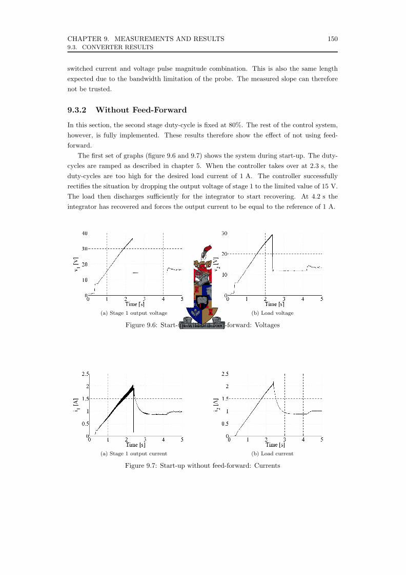
CHAPTER 9. MEASUREMENTS AND RESULTS 1509.3. CONVERTER RESULTS
switched current and voltage pulse magnitude combination. This is also the same lengthexpected due to the bandwidth limitation of the probe. The measured slope can thereforenot be trusted.
9.3.2 Without Feed-Forward
In this section, the second stage duty-cycle is fixed at 80%. The rest of the control system,however, is fully implemented. These results therefore show the effect of not using feed-forward.
The first set of graphs (figure 9.6 and 9.7) shows the system during start-up. The duty-cycles are ramped as described in chapter 5. When the controller takes over at 2.3 s, theduty-cycles are too high for the desired load current of 1 A. The controller successfullyrectifies the situation by dropping the output voltage of stage 1 to the limited value of 15 V.The load then discharges sufficiently for the integrator to start recovering. At 4.2 s theintegrator has recovered and forces the output current to be equal to the reference of 1 A.
(a) Stage 1 output voltage (b) Load voltage
Figure 9.6: Start-up without feed-forward: Voltages
(a) Stage 1 output current (b) Load current
Figure 9.7: Start-up without feed-forward: Currents

CHAPTER 9. MEASUREMENTS AND RESULTS 1519.3. CONVERTER RESULTS
The second set (figures 9.8 and 9.9) show the ripple on the measurements. No smoothingwas performed on these measurements.
The voltage spikes occur at a frequency of 190.735 kHz, which is half the second stageswitching frequency. It is also four times the switching frequency of stage 1. The cause isEMI and can be eliminated by using a more carefully laid out PCB design.
The current ripple on both the stage 1 output current and the load current is 47.684 kHz.This indicates that the very fast second stage switching frequency is filtered out by the L-Cfilter, whereas the lower stage 1 frequency is not. The final feed-forward implementationshould solve this problem.
The noise is due to the amplification of the small LEM module output signal. A betterquality amplifier positioned physically closer to the module will reduce this noise.
(a) Stage 1 output voltage (b) Load voltage
Figure 9.8: Ripple without feed-forward: Voltages
(a) Stage 1 output current (b) Load current
Figure 9.9: Ripple without feed-forward: Currents
The response to a 1 A to 2 A to 1 A step reference is provided by figures 9.10 and 9.11.The result is as predicted by simulation in figure 5.19 on page 78. The current shows a first-
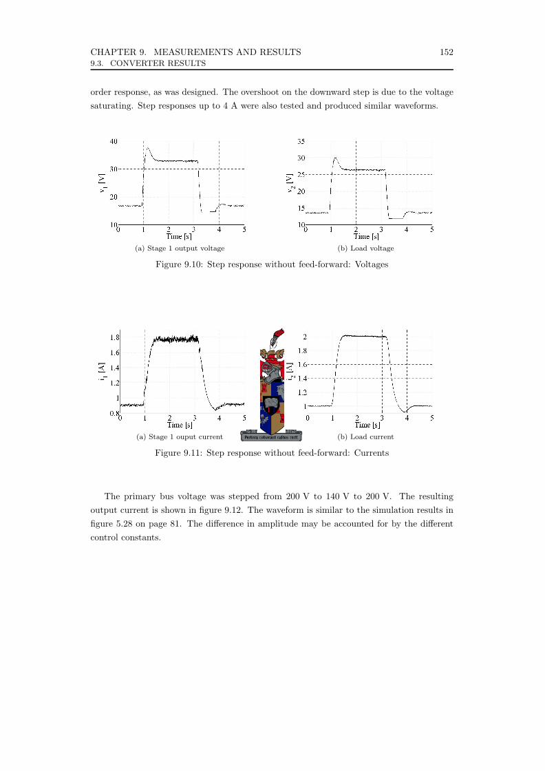
CHAPTER 9. MEASUREMENTS AND RESULTS 1529.3. CONVERTER RESULTS
order response, as was designed. The overshoot on the downward step is due to the voltagesaturating. Step responses up to 4 A were also tested and produced similar waveforms.
(a) Stage 1 output voltage (b) Load voltage
Figure 9.10: Step response without feed-forward: Voltages
(a) Stage 1 ouput current (b) Load current
Figure 9.11: Step response without feed-forward: Currents
The primary bus voltage was stepped from 200 V to 140 V to 200 V. The resultingoutput current is shown in figure 9.12. The waveform is similar to the simulation results infigure 5.28 on page 81. The difference in amplitude may be accounted for by the differentcontrol constants.

CHAPTER 9. MEASUREMENTS AND RESULTS 1539.3. CONVERTER RESULTS
Figure 9.12: Step disturbance without feed-forward
9.3.3 With Feed-Forward
The feed-forward strategy was tested first by providing a fixed v3 reference of 20 V. Theresulting voltages are shown in figure 9.13. As expected, the first stage output voltage settledon some value close to 25 V. It is lower than expected due to the line voltage being lower.The second stage provided the 20 V by means of feed-forward, cancelling out the effect ofthe lower line voltage. It is not exactly 20 V due to non-linear properties in the converter.
(a) Stage 1 output voltage (b) Stage 2 output voltage
Figure 9.13: Feed-forward voltage reference
The system was then started, as before, with ramped duty-cycles. The large overshootis not present because the duty-cycles do not ramp as high is in the previous section. Theresulting graphs are shown in figures 9.14 and 9.15.
It this case, the stage 1 filter capacitor was charged to 6 V at the start of the sequence.The second stage duty-cycle switched on at 0.3 s, discharging the capacitor into the secondstage inductor. The current spike is clearly visible at 0.3 s. The effect of the ramping stage1 duty-cycle is observed late due to the large stage 1 L-C filter.
The control system takes over at 1.35 s, where a small glitch is noticeable. The integratortakes effect at 1.8 s. The load current is settled on 1 A after 2.4 s.
The response to a 1 A to 2 A to 1 A to 3 A reference is shown by figures 9.16 and 9.17.

CHAPTER 9. MEASUREMENTS AND RESULTS 1549.3. CONVERTER RESULTS
(a) Stage 1 output voltage (b) Load voltage
Figure 9.14: Start-up with feed-forward: Voltages
(a) Stage 1 output current (b) Load current
Figure 9.15: Start-up with feed-forward: Currents
The 2 A step response is as expected, but the feed-forward seems to fail on the downwardstep. Both the first and second stage voltages show a flat area from 1.8 s to 2.4 s. Only thefirst stage voltage should be flat. The second stage voltage should be able to go down allthe way to zero. This indicates a mistake in the VHDL code.
While trying to respond to the 3 A step reference, the output current levels off too early.It seems to not be able to reach the required 3 A. This once again indicates an error in theVHDL code, since the converter could reach 4 A without a problem when feed-forward wasdisabled. The error will be investigated in future work.

CHAPTER 9. MEASUREMENTS AND RESULTS 1559.4. PROBE MEASUREMENTS
(a) Stage 1 output voltage (b) Load voltage
Figure 9.16: Step response with feed-forward: Voltages
(a) Stage 1 output current (b) Load current
Figure 9.17: Step response with feed-forward: Currents
9.4 Probe Measurements
9.4.1 Functionality
At the time of building the probe circuit, the analogue switch was excluded. Apart fromthis, the circuit is fully functional. The gain from DDS1 (the excitation signal) to the outputof the excitation mixer is 9 dB. The gain from the detection signal to the detection mixeroutput is 32 dB. Both of these are taken when the output of DDS2 (the mixing signal) isat full-scale.
9.4.2 Circuit Delays
A 4.125 m cable was used from the controller PCB to the probe and a 1.5 m cable returningto the controller. The total delay in the cable thus 28.125 ns, assuming that the speed ofthe signal is 2·108 m·s-1. Table 9-I shows the results of connecting the two cables togetherdirectly. Table 9-II shows the results of including the probe in the path.
These phase delays can easily be stored within a look-up table and simply subtracted

CHAPTER 9. MEASUREMENTS AND RESULTS 1569.5. SUMMARY
Table 9-I: Circuit delay (controller side)
Frequency Phase (lagging) Delay Circuit delay Circuit phase shift
[MHz] [deg] [ns] [ns] [deg]
5 55.7 30.94 2.815 5.067
10 111.0 30.83 2.705 9.738
20 218.0 30.28 2.155 15.516
Table 9-II: Circuit delay (Probe side)
Frequency Phase (lagging) Delay Probe delay Probe phase shift
[MHz] [deg] [ns] [ns] [deg]
5 57.1 31.72 0.78 1.404
10 124.0 34.44 3.61 12.996
20 274.7 38.15 7.87 56.664
from the measured phase in order to obtain the actual phase.
9.4.3 Glitches
One interesting observation to be noted is that every time the DDS is updated with newfrequency, phase and amplitude requirements, it produces a small glitch on the outputwaveform. This glitch has negligible effect if it occurs only once every 10 µs.
9.5 Summary
The converter was tested, but at a lower line-voltage. The control system is stable andperforms well when feed-forward control is disengaged. When feed-forward is used, thesystem becomes unstable for large output currents. An error within the VHDL code issuspected, but the exact cause is unclear and left to future investigation.
The probe circuit hardware was tested successfully, but no NMR effects were measured.

Chapter 10
Conclusions and Future Work
10.1 Introduction
This final chapter provides a summary of research findings, possible improvements for thenext iteration and future research topics.
10.2 Research Findings
10.2.1 Integration
All the digital control components of a typical modern magnet power supply were successfullyintegrated within a single FPGA. These include the control system, probe and interface.
Massive parallelisation within an FPGA enables the different digital componentsto execute at speeds. The implementation of very fast control schemes is possible.Implementing a system with 100 kHz bandwidth and a 100 ns time-step is no problem,provided the ADC is fast enough. This eases the migration process from a continuous- timedesign to a digital implementation.
10.2.2 Converter
In order to realise the precision required over the full output range, a dual stage convertertopology has been designed and implemented. The first stage successfully adjusts the inputto the second stage to 125% of the desired output voltage. From there the second stageeasily achieves the desired 10 ppm precision and stibility.
10.2.3 Digital Control
The only problem with digital control for high-precision systems is the resolution of theADCs. Resolution may be increased, but this is left to future research. The desired 10 ppmstability was not obtained using 18-bit ADCs, although the principle is verified.
157

CHAPTER 10. CONCLUSIONS AND FUTURE WORK 15810.3. IMPROVEMENTS AND FUTURE WORK
Feed-forward control provides an elegant way of increasing the rejection bandwidth of alow-bandwidth control system. The input disturbance is neutralised before it causes an effecton the output. Feedback control, in contrast, waits for the effect on the output to be presentbefore it can remove it. A feed-forward control strategy was successfully implemented.
10.2.4 Digital PWM
Two methods of increasing the resolution of digitally generated PWM was investigated. Itwas found that the noise shaper reigns superior over the delay-line. Some of the advantagesof the noise shaper are included in the following list:
• The ability to use any clock-frequency (as apposed to one dependant on the delay-lineinterval)
• Superior resolution (>18-bit) at a high switching frequency (>350 kHz)
• No external components are required
• Ease of implementation (a simple digital differentiator chain is required with unitygain)
• The high resolution required from the digital PWM (>18-bit) is easily reached witha 4th order noise shaper and 8-bit PWM generator. This is true provided that theswitching frequency is at least 36 times higher than the frequency at which theresolution is required.
10.2.5 Probe
A new NMR probe scheme was proposed, designed and simulated. The Lamour frequencyis followed by means of a phase-locked loop while the sample is kept in a continuouslyresonant state. The excitation signal is generated digitally and therefore the frequency ofresonance is immediately available. Also, it is best to use pure water as a sample so that thetime-constants T1 and T2 are as large as possible. This solves the problem of crystallisation.
Measurement rate may be increased to 100 ksps. A magnetic field-strength ramp of10 T·s-1 can be followed with negligible error. Direct NMR-measured field-strength feedbackis thus practical. Much research and development remains, however.
10.3 Improvements and Future Work
10.3.1 Converter
The soft-start may be implemented differently. The three triacs and diode-bridge may bereplaced with the circuit in figure 10.1. This prevents unnecessary use of three components.The soft-charge resistor bypass MOSFET may also be replaced with a triac. The drivingcircuit is then much simpler.

CHAPTER 10. CONCLUSIONS AND FUTURE WORK 15910.3. IMPROVEMENTS AND FUTURE WORK
Chapter 10 – Conclusions and Future Work : Improvements and Future Work 151
10.1.4 Digital PWM Two methods of increasing the resolution of digitally generated PWM has been investigated. It
was found that the noise shaper reigns superior over the delay-line. Some of the advantages of the
noise shaper are included in the following list:
• The ability to use any clock-frequency (as apposed to one dependant on the delay-line interval)
• Superior resolution (>18-bit) at a high switching frequency (>350kHz)
• No external components are required
• Ease of implementation (a simple digital differentiator chain is required with unity gain)
• The high resolution required from the digital PWM (>18-bit) is easily reached with a 4th order
noise shaper and 8-bit PWM generator. This is true provided that the switching frequency is at
least 143 times higher than the frequency at which the resolution is required.
10.1.5 Probe A new NMR probe scheme has been proposed, designed and simulated. The Lamour frequency
is followed by means of a phase-locked loop while the sample is kept in a continuously resonant state.
The excitation signal is generated digitally and therefore the frequency of resonance is immediately
available.
Measurement rate may be increased to 100ksps. A magnetic field-strength ramp of 10T·s-1 can be
followed with negligible error. Direct NMR-measured field-strength feedback is thus practical. Much
research and development remains, however.
10.2 Improvements and Future Work 10.2.1 Converter
The soft-start may be implemented differently. The three triacs and diode-bridge may be replaced
with the circuit in figure 10.1. This prevents unnecessary use of three components. The soft-charge
resistor bypass MOSFET may also be replaced with a triac. The driving circuit is then much simpler.
3-phase Mains
Figure 10.1 – New soft-start circuit
Another improvement would be to implement the second stage with a full-bridge converter. The
project would then be more versatile by providing bi-directional output current.
Figure 10.1: Proposed soft-start circuit
Another improvement would be to implement the second stage with a full-bridgeconverter. The project would then be more versatile by providing bi-directional outputcurrent.
10.3.2 Control System
With greater insight into the requirements of analogue to digital conversion it is possible tooptimise the choice of IC. Current i2 must have a higher resolution, but does not require ahigh sample rate. Current i1 and voltage v2 require a high sample rate, but not necessarilya good resolution. Voltage v1 requires superior resolution and sample rate, and might beimproved by the addition of a digital potentiometer. The input to the ADC can then beenlarged for smaller signals, improving their resolution while still using a practical ADC.
The control system implementation can be improved by using a finite state machineinstead of an asynchronous implementation. The same few multipliers may then be used toimplement many gain blocks. Higher resolution is then possible, through the availability ofmore multipliers.
An estimator (Kalman filter [26]) can be implemented to improve the quality ofmeasurement. This means that the only two high-resolution measurements are v1 and theflux density. A low-resolution measurement of v2 may be used to characterise the load.
10.3.3 PWM Generator
Future research in the area of PWM generation could include the optimisation of the noise-shaper. A lower-order noise-shaper may provide satisfactory results.
10.3.4 Probe
Much research is outstanding regarding the probe. The phase-locked loop must be optimised(by modifying D(z)) in order to follow a faster-changing flux density.
Resonance may be maintained by means of an analogue circuit (as explained in chapter7). This simplifies the task of the FPGA, but remains to be verified practically.
Also, the probe circuit may be considerably simplified (as explained in section 7.4), byimplementing the DDS within the FPGA. Problems associated by using a square waveform,such as harmonic content and sampling effects, remains to be investigated experimentally.

CHAPTER 10. CONCLUSIONS AND FUTURE WORK 16010.4. LEARNING EXPERIENCE
10.3.5 Controller
The most obvious improvement is the use of a power supply that requires less quiescentcurrent. This would decrease overall losses.
The analogue signals can be sent to the controller board using differential signals.Advantages include the absence of ground-loops, greater noise immunity and the ability touse a standard RJ-45 connector with CAT-5 network cable. ADCs generally have differentialinputs, so no further conversion would be required. The use of an external processor hasnumerous advantages and must be considered strongly for the next iteration, as mentionedin section 8.5.1.
10.4 Learning Experience
Much has been learned outside the scope of this project. Many mistakes were made duringthe planning phase and skills in this area have improved greatly. The overall scope of theproject was found to be too great for a single inexperienced person to complete fully intwo years. The experience gained, however, would without doubt prove invaluable in futureprojects.
10.5 Summary
The research objectives set out in chapter 1 were met theoretically. Practical verification,however, is not complete.
The implementation of the control system have been verified successfully. Problemsassociated with EMI effects have not been solved.
A new NMR measurement strategy has been designed and verified successfully throughsimulation. No practical results are available.
As a final conclusion, the project was greatly enjoyed and much valuable experience hasbeen gained.

Bibliography
[1] Pozar, D.M.: Microwave and RF design of Wireless Systems. John Wiley & Sons, 2001.
[2] Serway, R.A. and Beichner, R.J.: Physics for Scientists and Engineers with ModernPhysics. 5th edn. Prentice Hall, 2000.
[3] Hassanzadegan, H.: Digital Regulation of Accelerator Power Supplies. Availableat: http://www.epn-online.com/popup.php?content=page&page=11401&print=1,[25 February 2005].
[4] Liu, K. and Fann, C.: Reducing Output Current Ripple of Power Supply withComponent Replacement. In: Proceedings of EPAC. Lucerne, Switzerland, 2004.
[5] Haus, H.A. and Melcher, J.R.: Electromagnetic Fields and Energy. Prentice Hall, 1989.
[6] Mohan, N., Undeland, T.M. and Robbins, W.P.: Power Electronics. John Wiley &Sons, 2003.
[7] Starkey, J.R. and Irving, C.F.: NMR Analysing Magnet Controller MK II. NECSA,1978. Van der Graaff Accelerator Document Archive: EL 455 I/TN/35/78.
[8] Liang, R. and Dewan, S.B.: A Low Ripple Power Supply for High-Current MagnetLoad. IEEE Transactions on Industry Applications, vol. 30, no. 4, pp. 1006–1015,July/August 1994.
[9] Liang, R. and Dewan, S.B.: Modeling and Control of Magnet Power Supply Systemwith Switch-Mode Ripple Regulator. IEEE Transactions on Industry Applications,vol. 31, no. 2, pp. 264–272, March/April 1995.
[10] Qi, X. and Xu, Z.: Resonant Magnet Power Supply System for the Rapid CycleSynchrotron of Chinese Spallation Neutron Source. In: Proceedings of APAC. Gyeongiu,Korea, 2004.
[11] Bellomo, P., Berndt, M., de Lira, A., Leyh, G., Lipari, J.J., Rafael, F. and Widmeyer,M.: Spear 3 DC Magnet Power Supplies – an Overview. In: Proceedings of APAC.Gyeongiu, Korea, 2004. SLAC-PUB-10383.
[12] Wang, J.: A New Current Regulator for the APS Storage Ring Correction MagnetBipolar Switching Mode Converters. In: Proceedings of EPAC. Lucerne, Switzerland,2004.
[13] Jacobs, D.: Digital Pulse Width Modulation for Class-D Audio Amplifiers. Master’sthesis, Electronic Engineering, University of Stellenbosch, Stellenbosch, South Africa,2006.
[14] Franklin, G.F., Powell, J.D. and Emami-Naeini, A.: Feedback Control of DynamicSystems. 3rd edn. Addison-Wesley Publishing, 1994.
161
BIBLIOGRAPHY 162
[15] The Hall Effect. Available at: http://www.tf.unikiel.de/matwis/amat/mw2_ge/kap_2/backbone/r2_1_3.html, [17 August 2005].
[16] Beltran, D., Bordas, J., Campmany, J., Molins, A., Perlas, J.A. and Traveria, M.:An Instrument for Precision Magnetic Measurements of Large Magnetic Structures.Nuclear Instruments and Methods in Physics Research, Section A 459, pp. 285–294,2001.
[17] Cowan, B.: Nuclear Magnetic Resonance and Relaxation. Cambridge University Press,1997.
[18] Fei, X., Hughes, V.W. and Prigl, R.: Precision Measurement of the Magnetic Fieldin Terms of the Free-Proton NMR Frequency. Nuclear Instruments and Methods inPhysics Research, Section A 394, pp. 349–356, 1997.
[19] Meller, R.E. and Hartill, D.L.: Pulsed NMR magnetometers for CESR. Proceedings ofthe Particle Accelerator Conference, vol. 4, pp. 2339 – 2341, 2003.
[20] Prigl, R., Haeberlenb, U., Jungmann, K., Putlitz, G.Z. and von Walter, P.: A HighPrecision Magnetometer Based on Pulsed NMR. Nuclear Instruments and Methods inPhysics Research, Section A 374, pp. 118–126, 1996.
[21] Taylor, J., Mouton, H. du T. and Jones, T.: NMR-Controlled Analysing Magnet PowerSupply. In: Proceedings of SAUPEC. Durban, South Africa, 2006.
[22] Flowers, J.L., Franks, P.W. and Petley, B.W.: Correcting High Precision Pulsed NMRFlux Density Measurements for Asymmetries in the Lineshape. IEEE Transactions onInstrumentation and Measurement, vol. 44, no. 2, pp. 488–490.
[23] Nilsson, J.W. and Riedel, S.A.: Electric Circuits. 6th edn. Prentice-Hall, 2000.
[24] Sensitivity of Human Ear. Available at: http://hyperphysics.phy-astr.gsu.edu/hbase/sound/earsens.html, [13 February 2008].
[25] Wei, L., Lipo, T.A. and Chan, H.: Matrix Converter Topologies With Reduced Numberof Switches. In: Conference Record of the 20th WEMPEC Anniversary Meeting. 2001.
[26] Phillips, C.L. and Nagle, H.T.: Digital Contol System Analysis and Design. 3rd edn.Prentice Hall, 1995.
[27] Spiegel, M.R. and Liu, J.: Mathematical Handbook of Formulas and Tables. 2nd edn.McGraw-Hill, 1999.
[28] Peebles Jr, P.Z.: Probability, Random Variables and Random Signal Principles. 4thedn. McGraw-Hill, 2001.
[29] Proakis, J.G. and Manolakis, D.G.: Digital Signal Processing. 3rd edn. Prentice-Hall,1996.
[30] Zwolinski, M.: Digital System Design with VHDL. 2nd edn. Prentice Hall, 2004.
[31] Hanselman, D. and Littlefield, B.: The Student Edition of MATLAB Version 5 User’sGuide. PWS Publishing Company, 1997.
[32] Reader, H.C.: Vector network analyser circuit. Personal conversation, October 2006.
[33] On Semiconductor: 3.3 V ECL Programmable Delay Chip. Available at: http://www.onsemi.com/pub/Collateral/MC10EP195-D.PDF, [21 February 2005].

BIBLIOGRAPHY 163
[34] Neamen, D.A.: Electronic Circuit Analysis and Design. 2nd edn. McGraw-Hill, 2001.
[35] Microstrip Trace Impedance Calculator. Available at: http://www.emclab.umr.edu/pcbtlc/microstrip.html, [15 October 2005].
[36] Wolf, W.: Computers as Components. Morgan Kaufman Publishers, 2001.
[37] Goodrich, M.T. and Tamassia, R.: Data Structures and Algorithms in JAVAtm. 2ndedn. Wiley Publishers, 2001.
[38] Levitt, M.H.: Spin Dynamics. John Wiley & Sons, 2001.

Appendix A
Specification
A.1 Introduction
The specification listed in this appendix was presented to NECSA and approved by DrFranklyn.
A.2 Input From User
A.2.1 Analogue
• No analogue input is required from the user
A.2.2 Digital
• Source of digital input
– 4 x 4 Keypad
– RS232 (Standard DB-9 connector, 115200 baud)
– USB (Standard square USB connector) - Optional
– RS485 (Standard RJ-45 connector) - Optional
• Required flux density
– 0.1 T to 1.2 T, 1 µT steps
• Manual current override
– 1 A to 15 A, 10 µA steps
164

APPENDIX A. SPECIFICATION 165A.3. ACTIONS
A.3 Actions
• The system must ensure that the current through the magnet is such that the resultingfield has the desired flux density.
• The flux density must then be kept stable with fluctuations less than 10 ppm.
• In the case of manual current override, the current must be kept stable withfluctuations less than 500 ppm.
• The system must settle in less than 10 s upon switching on.
• The system must settle in less than 5 s upon any step change in required flux density.
A.4 Output to User
A.4.1 Analogue
• Clock used for calibration (Standard 50 Ω BNC connector)
• Magnet current (Analogue meter)
• Magnet voltage (Analogue meter)
A.4.2 Digital
• Source of digital output
– 16 x 4 LCD display
– RS232 (Standard DB-9 connector)
– USB (Standard square USB connector) - Optional
– RS485 (Standard DB-45 connector) - Optional
• Measured flux density
– <10 ppm error
• Measured current and voltage
– <1% error
• Field measurement unit status
– Is the probe reading within 10 ppm of the real value?
• Field control unit status
– Is the field locked within 10 ppm?

APPENDIX A. SPECIFICATION 166A.5. POWER
A.5 Power
• A 400 V, 13 kVA, 4-wire 3-phase connection is available for use by the current source.It is required to comply with ESKOM regulations.
A.6 Dimensions
A.6.1 Probe
• The probe must be 20 x 62 x 270 mm
• The field is perpendicular to the 62 x 270 mm face
A.6.2 Power Supply and Controller
• The power supply must be a standard 19′′ rack module, 4 units (7′′) high
A.7 Other
• All settings must me non-volatile.
• The NMR controller interfaces with the probe via a single 50 Ω co-axial line, connectedvia BNC on both ends. This cable is <30 m.
• The 20 A cable from the current source to the magnet is <30 m.
• High frequency (>100 kHz) ripple:
• The voltage ripple over the magnet must be less than 100 ppm
– The current ripple through the magnet must be less than 10 ppm
– The magnetic flux ripple of the magnet must not exceed 1 ppm.
– This is provided that the magnet has an inductance larger that 1 H throughoutthe frequency range of the ripple.
• The maximum current through the magnet must not exceed 15 A.
• The minimum current required through the magnet when active will not be less than1 A.
• The operating temperature range must be from 0 C to 40 C.

Appendix B
Formula Derivations
B.1 Introduction
This appendix provides the derivation of some of the equations mentioned in the chapters.
B.2 Inductor Design
Consider the inductor core shown in figure B.1a. It is assumed that the core has uniformwidth w and depth d throughout. Figure B.1b shows how the inductor is physicallyconstructed.
Error! No text of specified style in document. Error! No text of specified style in document. : Error! No
text of specified style in document. 1
w
d
2h
2al
N
i
w
Core
Effective area
d2ald +
2alw+
(a) Half an inductor core
Error! No text of specified style in document. Error! No text of specified style in document. : Error! No
text of specified style in document. 1
w
d
2h
2al
N
i
w
Core
Effective area
d2ald +
2alw+
(b) An inductor
Figure B.1: Inductor dimensions
The magnetic flux lines at the air-gap fringe, increasing the effective cross-sectionalarea Aa. According to [6], the effecting air-gap cross-sectional area dimensions may beapproximated as in figure B.2. The area Aa is therefore given by equation B.1.
Aa = (w +la2
)(d +la2
) (B.1)
167
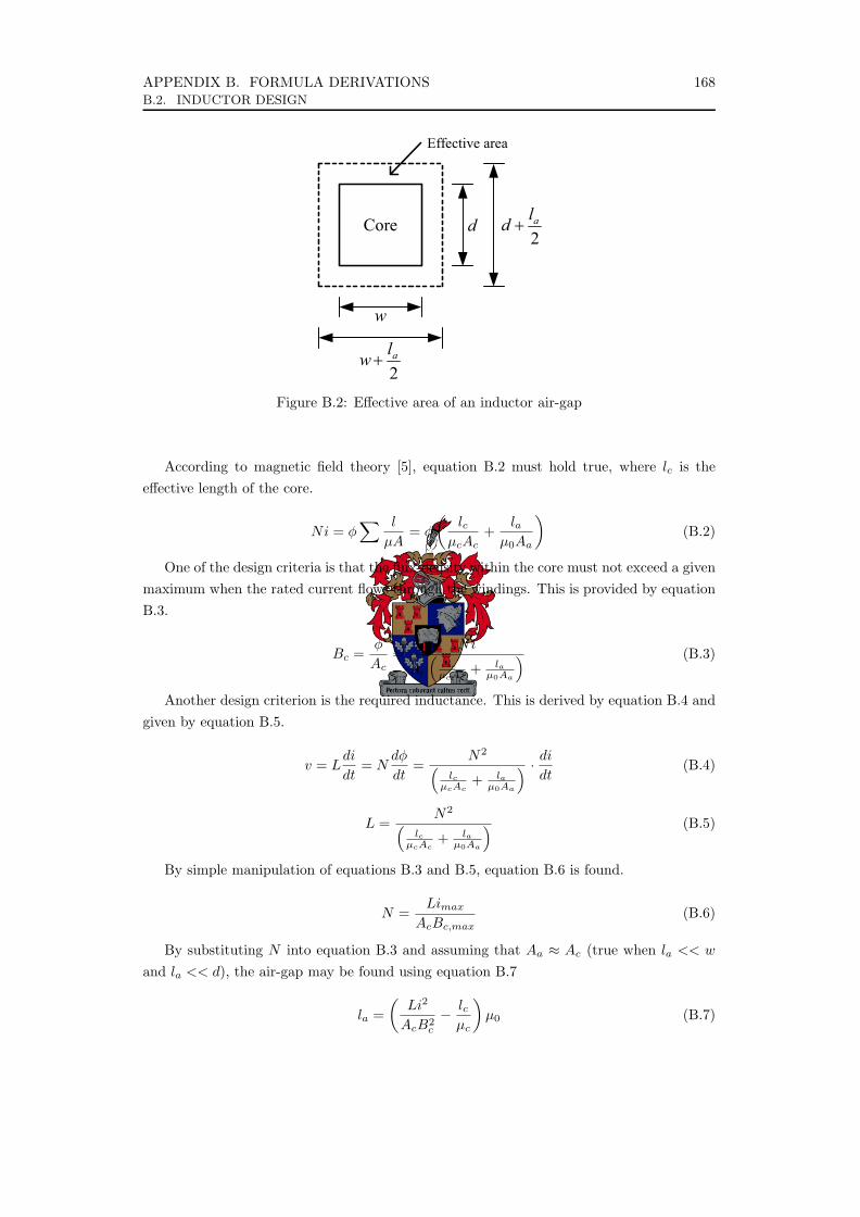
APPENDIX B. FORMULA DERIVATIONS 168B.2. INDUCTOR DESIGN
Error! No text of specified style in document. Error! No text of specified style in document. : Error! No
text of specified style in document. 1
w
d
2h
2al
N
i
w
Core
Effective area
d2ald +
2alw+
Figure B.2: Effective area of an inductor air-gap
According to magnetic field theory [5], equation B.2 must hold true, where lc is theeffective length of the core.
Ni = φ∑ l
µA= φ
(lc
µcAc+
laµ0Aa
)(B.2)
One of the design criteria is that the flux-density within the core must not exceed a givenmaximum when the rated current flows through the windings. This is provided by equationB.3.
Bc =φ
Ac=
Ni
Ac
(lc
µcAc+ la
µ0Aa
) (B.3)
Another design criterion is the required inductance. This is derived by equation B.4 andgiven by equation B.5.
v = Ldi
dt= N
dφ
dt=
N2(lc
µcAc+ la
µ0Aa
) · di
dt(B.4)
L =N2(
lcµcAc
+ laµ0Aa
) (B.5)
By simple manipulation of equations B.3 and B.5, equation B.6 is found.
N =Limax
AcBc,max(B.6)
By substituting N into equation B.3 and assuming that Aa ≈ Ac (true when la << w
and la << d), the air-gap may be found using equation B.7
la =(
Li2
AcB2c
− lcµc
)µ0 (B.7)

APPENDIX B. FORMULA DERIVATIONS 169B.3. TRANSFORMER DESIGN
The next step is to substitute the closest practical values for la and N into equationsB.3 and B.5 and finding the best solution iteratively. The same process can be followed inthe case of an E-core.
B.3 Transformer Design
The first consideration is to ensure that the core never saturates. A certain maximumflux density Bmax must not be exceeded. The voltage over the transformer primary is thesame as the bus voltage Vbus. This voltage may also be given by equation B.8 [6]. Aftermanipulation, the design equation B.9 results. The bus voltage is assumed constant.
Vbus = NAcoredB
dt(B.8)
N =Vbus
2BmaxAcorefs(B.9)
The next consideration is the maximum magnetising current im. This is given byequation B.10 [5]. By substituting equation B.9, equation B.11 results.
im =Bl
Nµ(B.10)
N =
√Vbuslcore
2µrµ0Acorefsim,max(B.11)
B.4 First Order Ramp Response
Figure B.3 shows an R-L system with feed-back control. It may be described by equationsB.12 and B.13.
Appendix B – Formula Derivations : Introduction 159
Appendix B – Formula Derivations
B.1 Introduction This appendix provides the derivation of some of the formulae mentioned in the chapters.
B.2 First Order Ramp Response Figure B.1 shows an R-L system with feed-back control. It may be described by equations B.1
and B.2.
irefN
∑
KLsR +
1iout
v
Figure B.1 – Single order R-L system with feedback
Lvi
LR
dtdi
outout +
−= (B.1)
refout NiKiv += (B.2)
By designing the system to have a zero steady-state error as well as a time-constant τ, equations
B.3 and B.4 are obtained.
RLK +−=τ
(B.3)
KRN −= (B.4)
A general ramp reference is given by equation B.5 where ‘m’ is the gradient of the ramp and ‘c’
the initial value. For a ramp reference ‘I0’ equals ‘c’. For a step reference, however, ‘c’ is the final
value of the step, ‘I0’ the initial value and ‘m’ is zero. Equations B.6 result from this reference.
cmtiref += (B.5)
)( cmtLNi
LKR
dtdi
outout ++
−−= (B.6)
Substituting equation B.4 and taking the Laplace transform of equation B.6 yields equation B.7.
KRNLscN
LsmNI
LNIIs −=++
−=− ,20 (B.7)
Figure B.3: Single order R-L system with feedback
diout
dt=
(−R
L
)iout +
v
L(B.12)
v = Kiout + Niref (B.13)
APPENDIX B. FORMULA DERIVATIONS 170B.5. FOURIER EXPANSIONS
By designing the system to have a zero steady state error as well as a time-constant τ ,equations B.14 and B.15 are obtained.
K = −L
τ+ R (B.14)
N = R −K (B.15)
A general ramp reference is given by equation B.16 where m is the gradient of the rampand c the initial value. For a ramp reference I0 equals c. For a step reference, however, c isthe final value of the step, I0 the initial value and m is zero. Equation B.17 result from thisreference.
iref = mt + c (B.16)
diout
dt=
(−R −K
L
)iout +
N
L(mt + c) (B.17)
Substituting equation B.15 and taking the Laplace transform of equation B.17 yieldsequation B.18.
Is− I0 =(−N
L
)I +
mN
Ls2+
cN
Ls,N = R −K (B.18)
Solving for I gives equation B.19. By using a partial fraction expansion (equation B.20)and taking the inverse Laplace transform yields equation B.21.
I =I0s
2 + cNL s + mN
L
s2(s + N
L
) (B.19)
I =m
s2+
(c− mL
N
)s +
(I0 − c +
mL
N
)1(
s + NL
) (B.20)
iout = mt +(
c− mL
N
)+
(I0 − c +
mL
N
)e−
NL t (B.21)
By substituting equations B.14 and B.15 into equation B.21, the general expression forthe ramp-response for any first-order system is obtained. This is given in equation B.22.
i = mt + c−mτ + (I0 − c + mτ)e−t/τ (B.22)
Also, the error signal can be obtained by using equation B.13.
B.5 Fourier Expansions
Equation B.23 shows the equation for rectified 400 V, 50 Hz 3-phase over a single period ofrectified waveform.

APPENDIX B. FORMULA DERIVATIONS 171B.5. FOURIER EXPANSIONS
f(t) = 565 cos(100πt) , t ∈(− 1
600,
1600
](B.23)
The Fourier expansion of the expression is given by equations B.24 to B.26 [27].
f(t) =a0
2+
∞∑n=1
(an cos(600nπt) + bn sin(600nπt)
)(B.24)
an = 600∫ 1
600
− 1600
f(t) cos(600nπt)dt (B.25)
bn = 600∫ 1
600
− 1600
f(t) sin(600nπt)dt (B.26)
By noting that f(t) is symmetrical about the y-axis, bn is zero for all n. Equation B.25can easily be solved to obtain equations B.27 and B.28 [27].
f(t) =a0
2+
∞∑n=1
an cos(12fLnπt) (B.27)
an =2400
√2
π
((−1)n(−4)
(12n− 2)(12n + 2)
)(B.28)

Appendix C
Theory of NMR
C.1 Introduction
In order to design an NMR probe, a deeper understanding of the physical processes must beachieved. This appendix delves into the physics of NMR. It also provides a brief explanationregarding popular measurement techniques. Unless otherwise noted, all equations andexplanations included in this appendix have been adapted from Nuclear Magnetic Resonanceand Relaxation [17] and Spin Dynamics [38].
On an atomic level, NMR is a quantum process. This detail is not important for thepurposes of this thesis, and therefore will not be discussed in much depth. The macroscopiceffect and mathematical models, on the other hand, are thoroughly perused.
C.2 Basic Principle
C.2.1 Proton Properties
Protons, like all atomic particles, spin. They also have a significant mass (1.673·10-27 kg) andcharge (160.218·10-21 C). There are numerous implications that result. First, any massiveobject that spins has angular momentum. It thus resists changing its axis of rotation.Also, because it is positively charged, there is a circular current flowing around the axis ofrotation. This current induces a magnetic moment (µ), given by equation C.1. The constantγ is termed the “gyromagnetic constant” of the particle in question and ~ the normalisedPlanck’s constant. A graphical representation is presented in figure C.1.
µ =γ~2
(C.1)
172
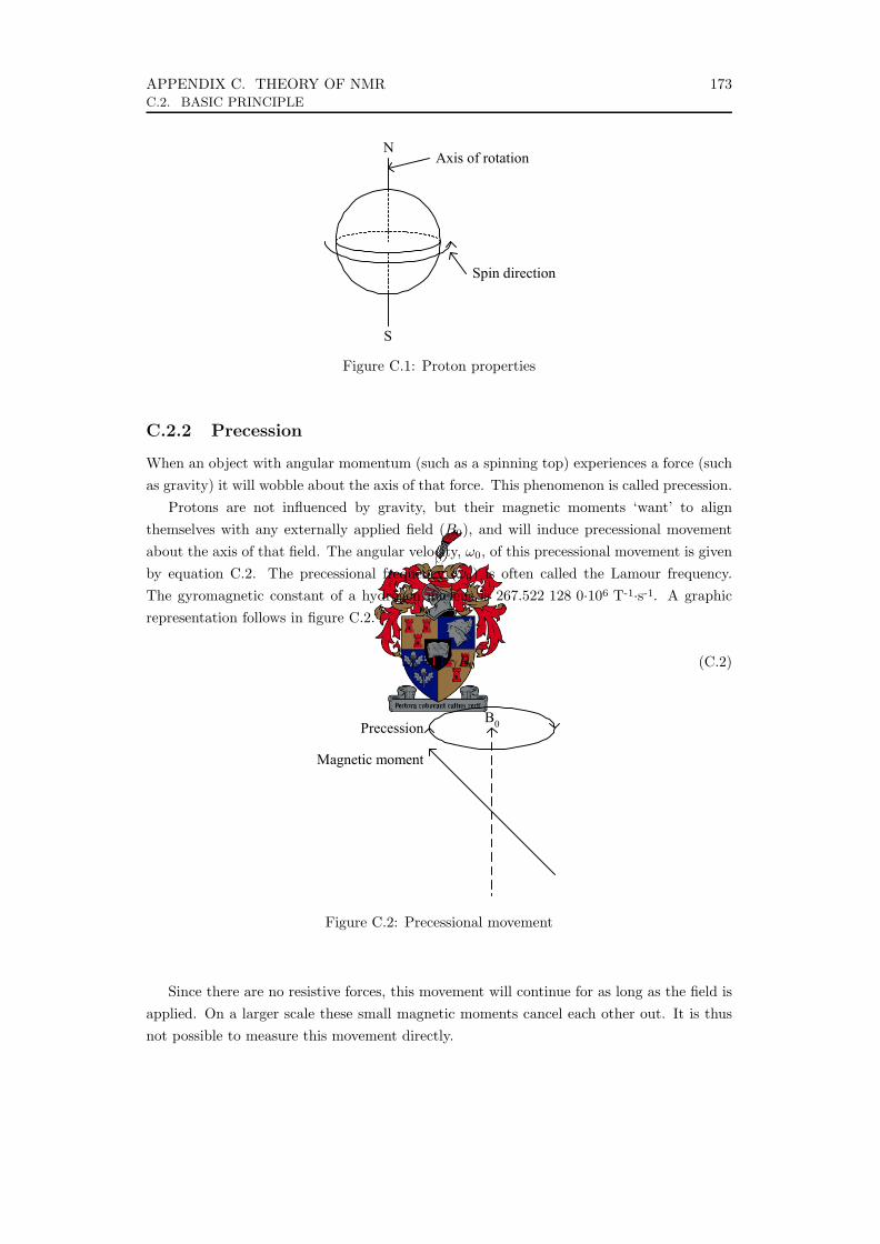
APPENDIX C. THEORY OF NMR 173C.2. BASIC PRINCIPLE
Appendix C – Theory of NMR : Introduction 162
Appendix C – Theory of NMR
C.1 Introduction In order to design an NMR probe, a deeper understanding of the physical processes must be
achieved. This appendix delves into the physics of NMR. It also provides a brief explanation
regarding popular measurement techniques. Unless otherwise noted, all formulae and explanations
included in this chapter have been adapted from Nuclear Magnetic Resonance and Relaxation [3] and
Spin Dynamics [12].
On an atomic level, NMR is a quantum process. This detail is not important for the purposes of
this thesis, and therefore will not be discussed in much depth. The macroscopic effect and
mathematical models, on the other hand, are thoroughly perused.
C.2 Basic Principle C.2.1 Proton Properties
Protons, like all atomic particles, spin. They also have a significant mass (1.673·10-27 kg) and
charge (160.218·10-21 C). There are numerous implications that result. First, any massive object that
spins has angular momentum. It thus resists changing its axis of rotation. Also, because it is positively
charged, there is a circular current flowing around the axis of rotation. This current induces a magnetic
moment (µ), given by equation C.1. The constant ‘γ’ is termed the “gyromagnetic constant” of the
particle in question and ‘ħ’ the normalised Planck’s constant. A graphical representation is presented in
figure C.1.
2hγµ =
(C.1)
Axis of rotation
Spin direction
N
S Figure C.1 – Proton properties Figure C.1: Proton properties
C.2.2 Precession
When an object with angular momentum (such as a spinning top) experiences a force (suchas gravity) it will wobble about the axis of that force. This phenomenon is called precession.
Protons are not influenced by gravity, but their magnetic moments ‘want’ to alignthemselves with any externally applied field (B0), and will induce precessional movementabout the axis of that field. The angular velocity, ω0, of this precessional movement is givenby equation C.2. The precessional frequency (ω0) is often called the Lamour frequency.The gyromagnetic constant of a hydrogen nucleus is 267.522 128 0·106 T-1·s-1. A graphicrepresentation follows in figure C.2.
ω0 = −γB0 (C.2)
Appendix C – Theory of NMR : Relaxation 163
C.2.2 Precession When an object with angular momentum (such as a spinning top) experiences a force (such as
gravity) it will wobble about the axis of that force. This phenomenon is called precession.
Protons are not influenced by gravity, but their magnetic moments ‘want’ to align themselves
with any externally applied field (B0), and will induce precessional movement about the axis of that
field. The angular velocity, ω0, of this precessional movement is given by equation C.2. The
precessional frequency (ω0) is often called the Lamour frequency. The gyromagnetic constant of a
hydrogen nucleus is 267.5221280·106 s-1·T-1. A graphic representation follows in figure C.2.
00 Bγω −= (C.2)
Magnetic moment
PrecessionB0
Figure C.2 – Precessional movement
Since there are no resistive forces, this movement will continue for as long as the field is applied.
On a larger scale these small magnetic moments cancel each other out. It is thus not possible to
measure this movement directly.
C.3 Relaxation C.3.1 Principle
Due to the temperature of the sample along with the presence of so many other particles, the
magnetic field experienced by each particle has a random component. This has the effect of biasing the
movement of each particle slightly in the direction of the external field. After a certain time, dictated
by T1 (the longitudinal time constant), a magnetization will develop. Magnetisation is defined as the
net magnetic moment per unit volume. This magnetization, M0, is given by equation C.3 where ‘Nv’ is
the number of protons per unit volume, ‘k’ Boltzmann’s constant and ‘T’ the temperature of the sample.
For small values of B0 (<300kT), equation C.3 is closely approximated by equation C.4. Substituting
equation C.1 yields equation C.5. This may be re-written by equation C.6 where ‘a0’ is the
proportionality constant.
Figure C.2: Precessional movement
Since there are no resistive forces, this movement will continue for as long as the field isapplied. On a larger scale these small magnetic moments cancel each other out. It is thusnot possible to measure this movement directly.

APPENDIX C. THEORY OF NMR 174C.3. RELAXATION
C.3 Relaxation
C.3.1 Principle
Due to the temperature of the sample along with the presence of so many other particles,the magnetic field experienced by each particle has a random component. This has theeffect of biasing the movement of each particle slightly in the direction of the external field.After a certain time, dictated by T1 (the longitudinal time constant), a magnetisation willdevelop. Magnetisation is defined as the net magnetic moment per unit volume. Thismagnetisation, M0, is given by equation C.3 where Nv is the number of protons per unitvolume, k Boltzmann’s constant and T the temperature of the sample. For small values of B0
(<300 kT), equation C.3 is closely approximated by equation C.4. Substituting equation C.1yields equation C.5. This may be re-written by equation C.6 where a0 is the proportionalityconstant.
M0 = Nvµ tanh(
~γB0
2kT
)(C.3)
M0 =Nvµ~γ
2kTB0 (C.4)
M0 =Nv~2γ2
4kTB0 (C.5)
M0 = a0B0 (C.6)
C.3.2 Time Constants
The longitudinal time constant T1 is given by equation C.7. The various constants are givenby equation C.8 to C.10. The constant a is the molecular radius of water and η the viscosity.
T−11 = γ2〈B2
x〉J(ω0) (C.7)
J(ω) =τc
1 + (ωτc)2(C.8)
τc =a2
6D(C.9)
D =kT
8πaη(C.10)
In equation C.7, 〈B2x〉 is the mean square amplitude of the random field Bx (typically
1.3·10-6 T2 for water at 20 C). T1 is approximately 3.6 s for pure water at 20 C. Bythe addition of paramagnetic ions the time constant T1 can be lowered to the order ofmilliseconds.
APPENDIX C. THEORY OF NMR 175C.4. PRECESSION IN AN RF FIELD
T2 is a similar time constant, approximately 4.7 s for pure water. It is called thetransverse relaxation time constant and is given by equation C.11. This time constantdictates the time it takes for a magnetisation vector in precession to decay to have acomponent only in the direction of the applied field. One can think of each of the particlesas a clock, started at the same time, with the second hand representing the direction ofthe magnetic moment in the x-y plane (the applied field is in the z-direction). After a longtime, due to random differences in period, the clocks will differ so much that the averagedirection of the hands will be zero.
T−12 =
320
b2 3J(0) + 5J(ω0) + 2J(2ω0) (C.11)
The constant b is the dipole-dipole coupling constant and is given by equation C.12. Thedistance between spins r may be greatly increased by the addition of impurities. The timeconstant T2 can thus also be reduced to be in the order of milliseconds.
b =−µ0~γ2
4πr3(C.12)
The other effect of increasing the distance between water molecules is that the hydrogendensity decreases. This means a decrease in M0 and thus a much smaller signal. Thedetection coil must then be more carefully designed and is often impedance-matched at thepoint of resonance. Large frequency range is implemented using varactor tuning diodes.
C.4 Precession in an RF Field
C.4.1 Principle
Say the applied magnetic field is still in the z-direction. This would mean that precessioncan be modelled by a magnetisation component rotating in the x-y plane. The magneticfield about which the magnetisation vector precesses can be altered by the addition of amagnetic field in the x-y plane. When this extra external field rotates about the z-axis,interesting things start to happen - especially when that field rotates at the same speed asthe precessional movement.
C.4.2 Bloch Equations
The Bloch equations describe in full the behaviour of the magnetisation vector under anapplied magnetic field. They are given by equations C.13 to C.15 and in matrix formin equation C.16. Mx, My and Mz are the magnetisation vector (M) in the x-, y- andz-directions respectively. Similarly, Bx, By and Bz are the components of the appliedmagnetic field (B).
dMx
dt= γ(MyBz −MzBy)− Mx
T2(C.13)
APPENDIX C. THEORY OF NMR 176C.4. PRECESSION IN AN RF FIELD
dMy
dt= γ(MzBx −MxBz)−
My
T2(C.14)
dMz
dt= γ(MxBy −MyBx)− Mz −M0
T1(C.15)
M = γ(M×B)−
Mx
T2My
T2Mz−M0
T1
(C.16)
The cross-product of M and B indicates that the movement progresses in a circularmotion around the axis of B. This corresponds to precession. The proportions of M thatare subtracted indicate movement towards a position in line with B and with magnitudeM0. This corresponds to relaxation.
C.4.3 Rotating Frame
In order to analyse the effect of an applied RF field, an axes-transformation may be made.The viewpoint in transformed in such a way as to rotate at the same speed about the z-axisas the applied RF field. This RF field is then seen as a constant field in the x-direction ofthe new ‘rotating frame’.
If the rotating frame rotates at the same rate as the precessional movement, theprecessional movement seems non-existent. The same effect can be achieved by loweringthe applied magnetic field in the z-direction. The equivalent magnetic field (Bz,eq) is thusgiven by equation C.17 where ω0 is the precession frequency and ωrf the frequency of therotating frame.
Bz,eq =ωrf − ω0
γ(C.17)
This new Bz,eq may then be substituted into the above Bloch equations in order to makethem valid within the rotating frame. The magnetisation vector now behaves under theinfluence of the equivalent applied magnetic field (Beq). It now rotates (or precesses) aboutBeq with angular velocity given by equation C.18.
ω = −γ |Beq| (C.18)
C.4.4 Applying the RF Field
From the explanations in the previous sections it may be assumed that a purely rotating RFfield is required. Such a field can be generated by using two coils to generate the separatex and y components. The two coils are then driven 90 out of phase in order to create arotating field in the x-y plane.
There is an easier way though. The effect of an RF field that rotates with the precessionalmovement lowers Bz,eq, whereas one rotating in the opposite direction increases Bz,eq. The
APPENDIX C. THEORY OF NMR 177C.5. CONTINUOUS WAVE NMR
RF field is typically smaller than 100 µT, whereas the applied constant field is typicallylarger than 1 T. This means that an RF field rotating opposite to the precessional movementhas negligible effect.
A pulsing RF field along the x-axis has two rotating components in the x-y plane. Thesetwo components rotate in opposite directions. The one rotating in the positive directionmay be ignored due to reasons explained in the previous paragraph. The rotating RF fieldto be considered thus has half the magnitude of the applied pulsed magnetic field.
From this point forward, Bx is the applied RF magnetic field rotating in the negativedirection within the x-y plane. Within the rotating frame it is stationary and pointing inthe positive x-direction. It has half the magnitude of the applied pulsed magnetic field.
C.4.5 Excitation Bandwidth
When the RF frequency is very close to the Lamour frequency, the magnetisation vectorprecesses about the x-axis. The idea is thus to deflect the magnetisation vector as much aspossible from the z-axis in order to be able to measure it.
The bandwidth of the excitation signal may be defined as the frequency range for whichthe maximum deflection is within 3 dB of the peak. The peak deflection is when the RFfrequency is exactly the same as the Lamour frequency.
One way to approach this problem mathematically is to note that the maximumdeflection starts to decrease at the point where Beq is 45 elevated from the x-y plane.This is when Bz,eq is the same as the applied Bx. The bandwidth in that case is given byequation C.19.
β = 2γBx (C.19)
Outside this narrow band the maximum deviation is given by equation C.20. It caneasily be derived by considering the path taken by the magnetisation vector graphically.
∆Mxy = M0 sin(
2 arctan(
γBx
ωrf + γB0
))(C.20)
The -3 db bandwidth is thus given by equation C.21, which may be approximated as4.82γBx.
β =2γBx
tan(
arcsin(10−3/20)2
) (C.21)
C.5 Continuous Wave NMR
C.5.1 Basic Principle
By exciting the sample using a very small signal (in the order of 1 nT) it is possible toinduce a steady state condition where the magnetisation vector remains at an angle withthe z-axis. This steady state condition is given by equations C.22 and C.23.
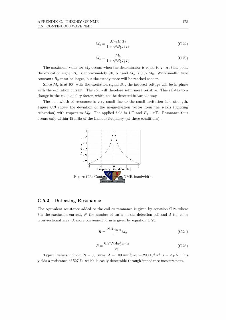
APPENDIX C. THEORY OF NMR 178C.5. CONTINUOUS WAVE NMR
My =M0γBxT2
1 + γ2B2xT1T2
(C.22)
Mz =M0
1 + γ2B2xT1T2
(C.23)
The maximum value for My occurs when the denominator is equal to 2. At that pointthe excitation signal Bx is approximately 910 pT and My is 0.57·M0. With smaller timeconstants Bx mast be larger, but the steady state will be reached sooner.
Since My is at 90 with the excitation signal Bx, the induced voltage will be in phasewith the excitation current. The coil will therefore seem more resistive. This relates to achange in the coil’s quality-factor, which can be detected in various ways.
The bandwidth of resonance is very small due to the small excitation field strength.Figure C.3 shows the deviation of the magnetisation vector from the z-axis (ignoringrelaxation) with respect to M0. The applied field is 1 T and Bx 1 nT. Resonance thusoccurs only within 45 mHz of the Lamour frequency (at these conditions).
Figure C.3: Continuous wave NMR bandwidth
C.5.2 Detecting Resonance
The equivalent resistance added to the coil at resonance is given by equation C.24 wherei is the excitation current, N the number of turns on the detection coil and A the coil’scross-sectional area. A more convenient form is given by equation C.25.
R =NAω0µ0
iMy (C.24)
R =0.57NAω2
0µ0a0
iγ(C.25)
Typical values include: N = 30 turns; A = 100 mm2; ω0 = 200·106 s-1; i = 2 µA. Thisyields a resistance of 527 Ω, which is easily detectable through impedance measurement.

APPENDIX C. THEORY OF NMR 179C.6. PULSED NMR
The problem with this setup is that the time constants are still in the order of seconds.This would not be a problem if the measurement could be made continuously. Themeasurement cannot be made continuously as the NMR signal is much smaller than inducedvoltage due to the coil inductance.
The solution is to sweep either the frequency (ωrf ) or B0 back and forth about theresonance point. This brings the coil in and out of resonance repetitively. The advantageof this is that AC-coupled amplifiers may be used to amplify the NMR signal and discardthe induced voltage due to inductance. The disadvantage is that the time constants mustbe decreased. This, as explained earlier, makes the NMR signal even smaller and thus moredifficult to detect. The detection coil must be carefully tuned using adjustable capacitorsor tuning diodes.
C.5.3 Field Measurement
The field strength is measured by determining the frequency of resonance. When the fieldstrength is swept and the frequency adjusted so that resonance occurs at the mid-pointof the field sweeping waveform, the frequency can be determined by means of a frequencycounter. Another alternative is to use a phase-locked loop in generating the RF signal. Theprogrammable counter value is then used to calculate the frequency.
C.6 Pulsed NMR
C.6.1 Basic Principle
The idea of pulsed NMR is to apply the RF field only long enough for the magnetisationvector to rotate through 90. In the stationary frame, the magnetisation vector then rotatesin the x-y plane and induces a current in the detection coil at exactly the Lamour frequency.By determining this frequency the field may be measured.
The time for which the RF field must be applied is given by equation C.26. An RF pulseof this length is called a π/2 pulse.
∆t =π
2γBx(C.26)
C.6.2 Determining the Frequency
Figure C.4 shows the maximum deviation of the magnetisation vector from the z-axis withrespect to M0. The applied magnetic field is 1 T and Bx is 100 µT. In order for the π/2pulse to result in a 90 rotation, the RF frequency must be within 4.26 kHz of the centrefrequency (in this case).
Determining the frequency at which to excite the sample is easy once the field-strengthis known, but the whole point is to measure the field strength using that frequency. Usinga calibrated current measurement to determine the field strength is only accurate to within0.1%. The resonance point must thus be found by trail-and-error.
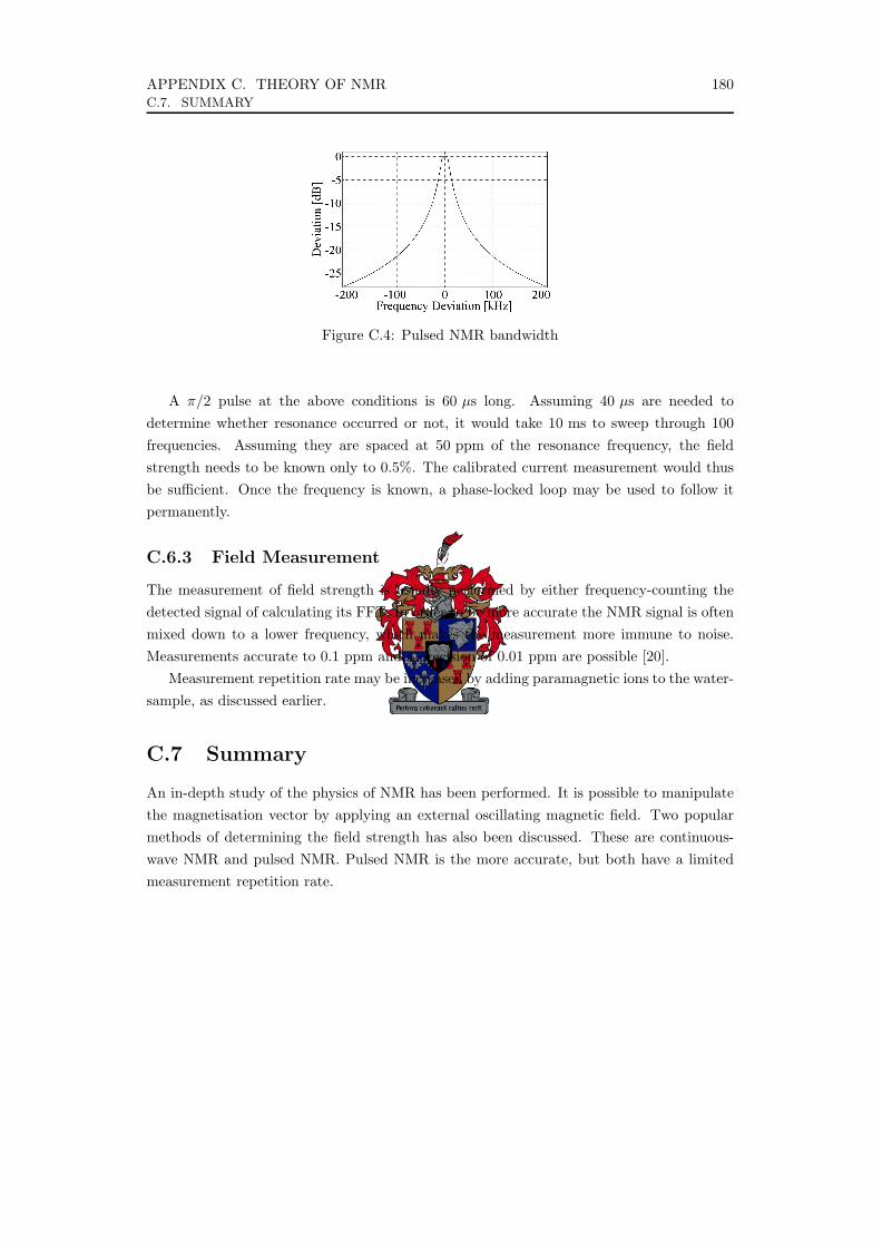
APPENDIX C. THEORY OF NMR 180C.7. SUMMARY
Figure C.4: Pulsed NMR bandwidth
A π/2 pulse at the above conditions is 60 µs long. Assuming 40 µs are needed todetermine whether resonance occurred or not, it would take 10 ms to sweep through 100frequencies. Assuming they are spaced at 50 ppm of the resonance frequency, the fieldstrength needs to be known only to 0.5%. The calibrated current measurement would thusbe sufficient. Once the frequency is known, a phase-locked loop may be used to follow itpermanently.
C.6.3 Field Measurement
The measurement of field strength is usually performed by either frequency-counting thedetected signal of calculating its FFT. In order to be more accurate the NMR signal is oftenmixed down to a lower frequency, which makes the measurement more immune to noise.Measurements accurate to 0.1 ppm and a precision of 0.01 ppm are possible [20].
Measurement repetition rate may be increased by adding paramagnetic ions to the water-sample, as discussed earlier.
C.7 Summary
An in-depth study of the physics of NMR has been performed. It is possible to manipulatethe magnetisation vector by applying an external oscillating magnetic field. Two popularmethods of determining the field strength has also been discussed. These are continuous-wave NMR and pulsed NMR. Pulsed NMR is the more accurate, but both have a limitedmeasurement repetition rate.

Appendix D
Circuit Diagrams
D.1 Introduction
This appendix presents the circuit diagrams designed for the prototype. The controller wasbuilt and tested as it is presented herein. A simplified version of the converter was built.
D.2 Controller
Figure D.1 shows the DDS circuitry, figure D.2 the analogue components, figure D.3 theFPGA and figure D.4 the other components.
D.3 Converter
The converter primary is presented in figure D.5 and the secondary in figure D.6.
D.4 Probe
The probe circuit is presented by figure D.7.
181
APPENDIX D. CIRCUIT DIAGRAMS 182
Figure D.1: DDS circuit diagram
APPENDIX D. CIRCUIT DIAGRAMS 183
Figure D.2: Analogue circuit diagram

APPENDIX D. CIRCUIT DIAGRAMS 184
Figure D.3: FPGA circuit diagram

APPENDIX D. CIRCUIT DIAGRAMS 185
Figure D.4: Other controller components circuit diagram
APPENDIX D. CIRCUIT DIAGRAMS 186
Figure D.5: Converter primary circuit diagram
APPENDIX D. CIRCUIT DIAGRAMS 187
Figure D.6: Converter secondary circuit diagram
APPENDIX D. CIRCUIT DIAGRAMS 188
Figure D.7: Probe circuit diagram

Appendix E
FPGA Source Code
E.1 Introduction
This appendix presents the FPGA code used for practical measurements. The first set(‘Interface’) is for the CPU and probe circuit. A PWM generator is included to test theprincipal. This set was implemented on the first iteration.
The second set (‘Controller’) is for the converter and was implemented on the seconditeration. The integration between these two is not complete. In both cases the top entityin the hierarchy is given first.
E.2 Interface
E.2.1 All Test
library ieee;
use ieee.std_logic_1164.all;
entity All_Test is
port(
Clk_125M : in std_logic; -- 125 MHz
nReset : in std_logic;
DDS_Reset : out std_logic;
DDS_IO_Update : out std_logic;
DDS_SCLK : out std_logic;
DDS_nCS1 : out std_logic;
DDS_nCS2 : out std_logic;
DDS_SDIO1 : out std_logic;
DDS_SDIO2 : out std_logic;
Delay0_D : out std_logic_vector(9 downto 0);
Delay0_In : out std_logic;
Delay0_Out : in std_logic;
Delay1_D : out std_logic_vector(9 downto 0);
Delay1_In : out std_logic;
Delay1_Out : in std_logic;
189
APPENDIX E. FPGA SOURCE CODE 190E.2. INTERFACE
DAC_DR : out std_logic;
DAC_DL : out std_logic;
DAC_Latch : out std_logic;
DAC_Clk : out std_logic;
ADC_Reset : out std_logic;
ADC_SClk : out std_logic;
ADC_nCS : out std_logic;
ADC_nCNVST : out std_logic;
ADC1_Busy : in std_logic;
ADC1_SDOUT : in std_logic;
ADC2_Busy : in std_logic;
ADC2_SDOUT : in std_logic;
ADC3_Busy : in std_logic;
ADC3_SDOUT : in std_logic;
ADC4_Busy : in std_logic;
ADC4_SDOUT : in std_logic;
S1 : out std_logic;
S2 : out std_logic;
S3 : out std_logic;
S4 : out std_logic;
LCD_RS : out std_logic;
LCD_E : out std_logic;
LCD_D : out std_logic_vector(7 downto 0);
LCD_BL : out std_logic;
Keypad_X : in std_logic_vector( 4 downto 1);
Keypad_Y : out std_logic_vector( 4 downto 1);
EEPROM_NCS : out std_logic_vector( 7 downto 0);
EEPROM_SCK : out std_logic;
EEPROM_SI : out std_logic;
EEPROM_SO : in std_logic;
RS232_Tx : out std_logic;
RS232_Rx : in std_logic;
LED_Error : out std_logic;
LED_Locked : out std_logic;
LED_F_High : out std_logic;
LED_F_Low : out std_logic;
LED_Reset : out std_logic; --Reset done
LED_Config : out std_logic --Config Done
);
end entity All_Test;
architecture a1 of All_Test is
component PLL is
port(
inclk0 : in std_logic;
c0 : out std_logic; --97 656 250.000 Hz
c1 : out std_logic; --78 125 000.000 Hz
locked : out std_logic
);
end component PLL;
component Global is
port(
a_in : in std_logic;
a_out: out std_logic
);
end component Global;

APPENDIX E. FPGA SOURCE CODE 191E.2. INTERFACE
component Counter5 is
port(
nReset: in std_logic;
Clk : in std_logic;
Q : out std_logic_vector(4 downto 0)
);
end component Counter5;
component Counter14 is
port(
nReset: in std_logic;
Clk : in std_logic;
Q : out std_logic_vector(13 downto 0)
);
end component Counter14;
component RealTime is
port(
nReset: in std_logic;
Clk : in std_logic; --9 765 625 Hz
Q : out std_logic_vector(7 downto 0)
);
end component RealTime;
component DAC is
port(
nReset : in std_logic;
Clock : in std_logic;
Data0 : in std_logic_vector(17 downto 0);
Data1 : in std_logic_vector(17 downto 0);
DR : out std_logic;
DL : out std_logic;
Latch : out std_logic;
Clk : out std_logic
);
end component DAC;
component ADC18 is
port(
nReset : in std_logic;
Clock : in std_logic;
Data1 : out std_logic_vector(17 downto 0);
Data2 : out std_logic_vector(17 downto 0);
Data3 : out std_logic_vector(17 downto 0);
Data4 : out std_logic_vector(17 downto 0);
Reset : out std_logic;
SClk : out std_logic;
nCS : out std_logic;
nCNVST : out std_logic;
Busy1 : in std_logic;
SDOUT1 : in std_logic;
Busy2 : in std_logic;
SDOUT2 : in std_logic;
Busy3 : in std_logic;
SDOUT3 : in std_logic;
Busy4 : in std_logic;
SDOUT4 : in std_logic
);
end component ADC18;
component Probe is
port(
nReset: in std_logic;

APPENDIX E. FPGA SOURCE CODE 192E.2. INTERFACE
Clk : in std_logic;
DDS_Reset : out std_logic;
DDS_IO_Update : out std_logic;
DDS_SCLK : out std_logic;
DDS_nCS1 : out std_logic;
DDS_nCS2 : out std_logic;
DDS_SDIO1 : out std_logic;
DDS_SDIO2 : out std_logic
);
end component Probe;
component PWM1 is
port(
nReset : in std_logic;
Clk : in std_logic; --97 656 250 Hz
Duty : in std_logic_vector(20 downto 0);
Delay_Out : out std_logic;
Delay_In : in std_logic;
Delay : out std_logic_vector(9 downto 0);
S1 : out std_logic;
S2 : out std_logic
);
end component PWM1;
component PWM2 is
port(
nReset : in std_logic;
Clk : in std_logic; --97 656 250 Hz
Duty : in std_logic_vector(17 downto 0);
Delay_Out : out std_logic;
Delay_In : in std_logic;
Delay : out std_logic_vector(9 downto 0);
S1 : out std_logic;
S2 : out std_logic
);
end component PWM2;
component LCD is
port(
nReset : in std_logic;
Clk : in std_logic;
Line : in std_logic_vector(1 downto 0);
Address : in std_logic_vector(4 downto 0);
Data : in std_logic_vector(7 downto 0);
Latch : in std_logic;
RS : out std_logic;
E : out std_logic;
D : out std_logic_vector(7 downto 0)
);
end component LCD;
component Keypad_Driver is
port(
nReset : in std_logic;
Clk : in std_logic;
Data : out std_logic_vector(7 downto 0); --Data(7) = Empty;
--Data(3 downto 0) = Key

APPENDIX E. FPGA SOURCE CODE 193E.2. INTERFACE
Ack : in std_logic;
X : in std_logic_vector( 4 downto 1);
Y : out std_logic_vector( 4 downto 1)
);
end component Keypad_Driver;
component Interface is
port(
nReset : in std_logic;
Clk : in std_logic;
Bus_R_nW : out std_logic;
Bus_Data : inout std_logic_vector(7 downto 0);
Bus_Address : out std_logic_vector(15 downto 0);
Bus_Latch : out std_logic
);
end component Interface;
component EEPROM is
port(
nReset : in std_logic;
Clk : in std_logic;
R_nW : in std_logic;
Data : inout std_logic_vector( 7 downto 0);
Address : inout std_logic_vector(15 downto 0);
Status : inout std_logic_vector( 1 downto 0); --read : write
DLatch : in std_logic;
A0Latch : in std_logic;
A1Latch : in std_logic;
SLatch : in std_logic;
NCS : out std_logic_vector( 7 downto 0);
SCK : out std_logic;
SI : out std_logic;
SO : in std_logic
);
end component EEPROM;
component COMM is
port(
nReset : in std_logic;
Clk : in std_logic; --9 765 625 Hz
R_nW : in std_logic;
Tx : inout std_logic_vector(7 downto 0);
Rx : out std_logic_vector(7 downto 0);
Status : inout std_logic_vector(7 downto 0);
TxLatch : in std_logic;
SLatch : in std_logic;
RS232_Tx : out std_logic;
RS232_Rx : in std_logic
);
end component COMM;
component InterfaceBus is
port(
nReset : in std_logic;
Clk : in std_logic; --The CPU clock
R_nW : in std_logic;
Data : inout std_logic_vector(7 downto 0);
Address : in std_logic_vector(15 downto 0);
APPENDIX E. FPGA SOURCE CODE 194E.2. INTERFACE
Latch : in std_logic;
LCD_Line : out std_logic_vector( 1 downto 0);
LCD_Address : out std_logic_vector( 4 downto 0);
LCD_Data : out std_logic_vector( 7 downto 0);
LCD_Latch : out std_logic;
LCD_BL : out std_logic;
EEPROM_R_nW : out std_logic;
EEPROM_Data : inout std_logic_vector( 7 downto 0);
EEPROM_Address : inout std_logic_vector(15 downto 0);
EEPROM_Status : inout std_logic_vector( 1 downto 0); --read:write
EEPROM_DLatch : out std_logic;
EEPROM_A0Latch : out std_logic;
EEPROM_A1Latch : out std_logic;
EEPROM_SLatch : out std_logic;
LED_Error : out std_logic;
LED_Locked : out std_logic;
LED_F_High : out std_logic;
LED_F_Low : out std_logic;
COMM_R_nW : out std_logic;
COMM_Tx : inout std_logic_vector(7 downto 0);
COMM_Rx : in std_logic_vector(7 downto 0);
COMM_Status : inout std_logic_vector(7 downto 0);
COMM_TxLatch : out std_logic;
COMM_SLatch : out std_logic;
Keypad : in std_logic_vector(7 downto 0);
Keypad_Ack : out std_logic;
RealTime : in std_logic_vector(7 downto 0)
);
end component InterfaceBus;
component Controller is
port(
nReset : in std_logic;
Clk : in std_logic;
--/**/ Controll registers to be put here
--/**/ Probe lines to be put here
PWM0 : out std_logic_vector(20 downto 0);
PWM1 : out std_logic_vector(17 downto 0);
DAC0 : out std_logic_vector(17 downto 0);
DAC1 : out std_logic_vector(17 downto 0);
ADC0 : in std_logic_vector(17 downto 0);
ADC1 : in std_logic_vector(17 downto 0);
ADC2 : in std_logic_vector(17 downto 0);
ADC3 : in std_logic_vector(17 downto 0)
);
end component Controller;
--Signals
signal tClk_97_656_250 : std_logic;
signal tClk_78_125_000 : std_logic;
signal Clk_97_656_250 : std_logic;
signal Clk_78_125_000 : std_logic;
signal Clk_48_828_125 : std_logic;

APPENDIX E. FPGA SOURCE CODE 195E.2. INTERFACE
signal Clk_24_414_063 : std_logic;
signal Clk_9_765_625 : std_logic;
signal Clk_3_051_758 : std_logic;
signal Clk_1_220_703 : std_logic;
signal Clk_4_768 : std_logic;
signal tnReset : std_logic;
signal Clk0_Temp : std_logic_vector( 5 downto 1);
signal Clk1_Temp : std_logic_vector(14 downto 1);
signal PLL_Locked : std_logic;
signal tPWM0 : std_logic_vector(20 downto 0);
signal tPWM1 : std_logic_vector(17 downto 0);
signal tDAC0 : std_logic_vector(17 downto 0);
signal tDAC1 : std_logic_vector(17 downto 0);
signal tADC0 : std_logic_vector(17 downto 0);
signal tADC1 : std_logic_vector(17 downto 0);
signal tADC2 : std_logic_vector(17 downto 0);
signal tADC3 : std_logic_vector(17 downto 0);
signal LCD_Line : std_logic_vector( 1 downto 0);
signal LCD_Address : std_logic_vector( 4 downto 0);
signal LCD_Data : std_logic_vector( 7 downto 0);
signal LCD_Latch : std_logic;
signal Keypad_Data : std_logic_vector(7 downto 0);
signal Keypad_Ack : std_logic;
signal EEPROM_R_nW : std_logic;
signal EEPROM_Data : std_logic_vector( 7 downto 0);
signal EEPROM_Address : std_logic_vector(15 downto 0);
signal EEPROM_Status : std_logic_vector( 1 downto 0);
signal EEPROM_DLatch : std_logic;
signal EEPROM_A0Latch : std_logic;
signal EEPROM_A1Latch : std_logic;
signal EEPROM_SLatch : std_logic;
signal COMM_R_nW : std_logic;
signal COMM_Tx : std_logic_vector(7 downto 0);
signal COMM_Rx : std_logic_vector(7 downto 0);
signal COMM_Status : std_logic_vector(7 downto 0);
signal COMM_TxLatch : std_logic;
signal COMM_SLatch : std_logic;
signal Bus_R_nW : std_logic;
signal Bus_Data : std_logic_vector(7 downto 0);
signal Bus_Address : std_logic_vector(15 downto 0);
signal Bus_Latch : std_logic;
signal RealTimeQ : std_logic_vector(7 downto 0);
begin
PLL1 : PLL port map(Clk_125M , tClk_97_656_250 , tClk_78_125_000 ,
PLL_Locked);
Count1 : Counter5 port map(tnReset , tClk_97_656_250 , Clk0_Temp);
Count2 : Counter14 port map(tnReset , tClk_78_125_000 , Clk1_Temp);
Global1 : Global port map(tClk_97_656_250 , Clk_97_656_250);
Global2 : Global port map(tClk_78_125_000 , Clk_78_125_000);
Global3 : Global port map(Clk0_Temp( 1) , Clk_48_828_125);
Global4 : Global port map(Clk0_Temp( 2) , Clk_24_414_063);
Global5 : Global port map(Clk1_Temp( 3) , Clk_9_765_625 );
Global6 : Global port map(Clk0_Temp( 5) , Clk_3_051_758 );
Global7 : Global port map(Clk1_Temp( 6) , Clk_1_220_703 );

APPENDIX E. FPGA SOURCE CODE 196E.2. INTERFACE
Global8 : Global port map(Clk1_Temp(14) , Clk_4_768 );
tnReset <= nReset;
RealTime1 : RealTime port map(tnReset , Clk_9_765_625 , RealTimeQ);
DAC1 : DAC port map(tnReset , Clk_24_414_063 , tDAC0 , tDAC1 ,
DAC_DR , DAC_DL , DAC_Latch , DAC_Clk);
ADC1 : ADC18 port map(tnReset , Clk_48_828_125 , tADC0 , tADC1 , tADC2 , tADC3 ,
ADC_Reset , ADC_SClk , ADC_nCS , ADC_nCNVST ,
ADC1_Busy , ADC1_SDOUT ,
ADC2_Busy , ADC2_SDOUT ,
ADC3_Busy , ADC3_SDOUT ,
ADC4_Busy , ADC4_SDOUT);
Probe1 : Probe port map(tnReset , Clk_3_051_758 ,
DDS_Reset , DDS_IO_Update , DDS_SCLK ,
DDS_nCS1 , DDS_nCS2 ,
DDS_SDIO1 , DDS_SDIO2);
PWM1_1 : PWM1 port map(tnReset , Clk_97_656_250 , tPWM0 ,
Delay0_In , Delay0_Out , Delay0_D , S1, S2);
PWM2_1 : PWM2 port map(tnReset , Clk_97_656_250 , tPWM1 ,
Delay1_In , Delay1_Out , Delay1_D , S3, S4);
LCD1 : LCD port map(tnReset , Clk_3_051_758 ,
LCD_Line , LCD_Address , LCD_Data , LCD_Latch ,
LCD_RS , LCD_E , LCD_D);
Keypad1 : Keypad_Driver port map(tnReset , Clk_4_768 ,
Keypad_Data , Keypad_Ack ,
Keypad_X , Keypad_Y);
Interface1 : Interface port map(tnReset , Clk_1_220_703 ,
Bus_R_nW , Bus_Data , Bus_Address , Bus_Latch);
EEPROM1 : EEPROM port map(tnReset , Clk_9_765_625 ,
EEPROM_R_nW , EEPROM_Data , EEPROM_Address ,
EEPROM_Status , EEPROM_DLatch ,
EEPROM_A0Latch , EEPROM_A1Latch , EEPROM_SLatch ,
EEPROM_NCS , EEPROM_SCK , EEPROM_SI , EEPROM_SO);
COMM1 : COMM port map(tnReset , Clk_9_765_625 ,
COMM_R_nW , COMM_Tx , COMM_Rx , COMM_Status ,
COMM_TxLatch , COMM_SLatch ,
RS232_Tx , RS232_Rx);
Bus1 : InterfaceBus port map(tnReset , Clk_1_220_703 ,
Bus_R_nW , Bus_Data , Bus_Address , Bus_Latch ,
LCD_Line , LCD_Address ,
LCD_Data , LCD_Latch , LCD_BL ,
EEPROM_R_nW , EEPROM_Data , EEPROM_Address ,
EEPROM_Status , EEPROM_DLatch ,
EEPROM_A0Latch , EEPROM_A1Latch , EEPROM_SLatch ,
LED_Error , LED_Locked , LED_F_High , LED_F_Low ,
COMM_R_nW , COMM_Tx , COMM_Rx , COMM_Status ,
COMM_TxLatch , COMM_SLatch ,
Keypad_Data , Keypad_Ack ,
RealTimeQ);
Controller1 : Controller port map(tnReset , Clk_1_220_703 ,
tPWM0 , tPWM1 ,
tDAC0 , tDAC1 ,
tADC0 , tADC1 , tADC2 , tADC3);
APPENDIX E. FPGA SOURCE CODE 197E.2. INTERFACE
LED_Reset <= tnReset;
LED_Config <= PLL_Locked;
end architecture a1;
E.2.2 ADC18
library ieee;
use ieee.std_logic_1164.all;
use ieee.std_logic_unsigned.all;
entity ADC18 is
port(
nReset : in std_logic;
Clock : in std_logic;
Data1 : out std_logic_vector(17 downto 0);
Data2 : out std_logic_vector(17 downto 0);
Data3 : out std_logic_vector(17 downto 0);
Data4 : out std_logic_vector(17 downto 0);
Reset : out std_logic;
SClk : out std_logic;
nCS : out std_logic;
nCNVST : out std_logic;
Busy1 : in std_logic;
SDOUT1 : in std_logic;
Busy2 : in std_logic;
SDOUT2 : in std_logic;
Busy3 : in std_logic;
SDOUT3 : in std_logic;
Busy4 : in std_logic;
SDOUT4 : in std_logic
);
end entity ADC18;
architecture a1 of ADC18 is
signal state : std_logic_vector( 2 downto 0);
signal count : std_logic_vector( 4 downto 0);
signal Busy : std_logic;
signal Temp1 : std_logic_vector(17 downto 0);
signal Temp2 : std_logic_vector(17 downto 0);
signal Temp3 : std_logic_vector(17 downto 0);
signal Temp4 : std_logic_vector(17 downto 0);
signal Cp1 : std_logic_vector( 4 downto 0);
begin
Reset <= not nReset;
-- Busy <= Busy1 or Busy2 or Busy3 or Busy4;
Busy <= Busy1 or Busy4; --only these two are installed
nCS <= '0';Cp1 <= Count + '1';
process(Clock , nReset) is
begin
if nReset = '0' then
state <= "000";
count <= "00000";
SClk <= '0';nCNVST <= '1';Temp1 <= "000000000000000000";
Temp2 <= "000000000000000000";
Temp3 <= "000000000000000000";
Temp4 <= "000000000000000000";
elsif rising_edge(Clock) then
case state is
when "000" =>

APPENDIX E. FPGA SOURCE CODE 198E.2. INTERFACE
if count = "11111" then
state <= "001";
end if;
count <= Cp1;
when "001" =>
count <= "00000";
if Busy = '0' then
nCNVST <= '0';state <= "010";
end if;
when "010" =>
nCNVST <= '1';SClk <= '1';Temp1(17 downto 1) <= Temp1(16 downto 0);
Temp2(17 downto 1) <= Temp2(16 downto 0);
Temp3(17 downto 1) <= Temp3(16 downto 0);
Temp4(17 downto 1) <= Temp4(16 downto 0);
Count <= Cp1;
state <= "011";
when "011" =>
SClk <= '0';Temp1(0) <= SDOUT1;
Temp2(0) <= SDOUT2;
Temp3(0) <= SDOUT3;
Temp4(0) <= SDOUT4;
if count = "10010" then --18
state <= "100";
else
state <= "010";
end if;
when "100" =>
Data1 <= Temp1;
Data2 <= Temp2;
Data3 <= Temp3;
Data4 <= Temp4;
state <= "001";
when others =>
end case;
end if;
end process;
end architecture a1;
E.2.3 Adder
library ieee;
use ieee.std_logic_1164.all;
use ieee.std_logic_unsigned.all;
entity Adder is
port(
A : in std_logic_vector(7 downto 0);
B : in std_logic_vector(8 downto 0);
Carry_In : in std_logic;
Y : out std_logic_vector(7 downto 0);
Carry : out std_logic
);
end entity Adder;
architecture a1 of Adder is
signal tY : std_logic_vector(8 downto 0);
begin
tY <= A + B + Carry_In;
Y <= tY(7 downto 0);
Carry <= tY(8);

APPENDIX E. FPGA SOURCE CODE 199E.2. INTERFACE
end architecture a1;
E.2.4 Alternator
library ieee;
use ieee.std_logic_1164.all;
entity Alternator is
port(
nReset: in std_logic;
PWM : in std_logic;
S1 : out std_logic;
S2 : out std_logic
);
end entity Alternator;
architecture a1 of Alternator is
signal Q: std_logic_vector(1 downto 0);
begin
process(PWM, nReset) is
begin
if nReset = '0' then
Q <= "01";
elsif falling_edge(PWM) then
case Q is
when "01" =>
Q <= "10";
when "10" =>
Q <= "01";
when others =>
end case;
end if;
end process;
S1 <= Q(0) and PWM and nReset;
S2 <= Q(1) and PWM and nReset;
end architecture a1;
E.2.5 Arith
library ieee;
use ieee.std_logic_1164.all;
use ieee.std_logic_unsigned.all;
entity Arith is
port(
A : in std_logic_vector(7 downto 0);
B : in std_logic_vector(7 downto 0);
Task : in std_logic_vector(3 downto 0);
Carry_In : in std_logic;
Zero_In : in std_logic;
Y : out std_logic_vector(7 downto 0);
Carry : out std_logic;
Zero : out std_logic
);
end entity Arith;
architecture a1 of Arith is
component Adder is
port(
A : in std_logic_vector(7 downto 0);
B : in std_logic_vector(8 downto 0);
Carry_In : in std_logic;
Y : out std_logic_vector(7 downto 0);
APPENDIX E. FPGA SOURCE CODE 200E.2. INTERFACE
Carry : out std_logic
);
end component Adder;
signal A_B : std_logic_vector(8 downto 0);
signal A_C_In : std_logic;
signal A_Y : std_logic_vector(7 downto 0);
signal A_C : std_logic;
signal tY : std_logic_vector(7 downto 0);
signal Y3 : std_logic_vector(7 downto 0);
signal Y4 : std_logic_vector(7 downto 0);
signal Y5 : std_logic_vector(7 downto 0);
signal Y6 : std_logic_vector(7 downto 0);
signal Y9 : std_logic_vector(7 downto 0);
signal Y10 : std_logic_vector(7 downto 0);
signal Y11 : std_logic_vector(7 downto 0);
signal Y12 : std_logic_vector(7 downto 0);
signal Y13 : std_logic_vector(7 downto 0);
signal Y14 : std_logic_vector(7 downto 0);
signal Y15 : std_logic_vector(7 downto 0);
signal tC : std_logic;
signal tZ : std_logic;
signal C10 : std_logic;
signal C11 : std_logic;
begin
Addd1 : Adder port map(A, A_B, A_C_In , A_Y, A_C);
with Task select
A_B(8) <= '1' when "0111" | "1000",
'0' when others;
A_B(7 downto 0) <= (not B) when A_B(8) = '1' else B;
with Task select
tC <= Carry_In when "0001" | "0111",
'0' when others;
A_C_In <= (not tC) when A_B(8) = '1' else tC;
Y3 <= A and B;
Y4 <= Y5 + '1';Y5 <= not A;
Y6 <= A or B;
Y9 <= A xor B;
C10 <= A(7); Y10(7 downto 1) <= A(6 downto 0); Y10(0) <= Carry_In;
C11 <= A(0); Y11(6 downto 0) <= A(7 downto 1); Y11(7) <= Carry_In;
Y12(7 downto 1) <= A(6 downto 0); Y12(0) <= A(7);
Y13(6 downto 0) <= A(7 downto 1); Y13(7) <= A(0);
Y14(7 downto 1) <= A(6 downto 0); Y14(0) <= Carry_In;
Y15(6 downto 0) <= A(7 downto 1); Y15(7) <= Carry_In;
with Task select
tY <= A_Y when "0001" | "0010" | "0111" | "1000",
Y3 when "0011",
Y4 when "0100",
Y5 when "0101",
Y6 when "0110",
Y9 when "1001",
Y10 when "1010",
Y11 when "1011",
Y12 when "1100",
Y13 when "1101",
Y14 when "1110",
APPENDIX E. FPGA SOURCE CODE 201E.2. INTERFACE
Y15 when "1111",
A when others;
Y <= tY;
tZ <= '1' when tY = "00000000" else '0';Zero <= Zero_In when Task = "0000" else tZ ;
with Task select
Carry <= A_C when "0001" | "0010" | "0111" | "1000",
C10 when "1010",
C11 when "1011",
Carry_In when others;
end architecture a1;
E.2.6 COMM
library ieee;
use ieee.std_logic_1164.all;
use ieee.std_logic_unsigned.all;
--/**/Give a FIFO queue - received remains low when queue is empty -
-- 512 bytes long in M4K block
entity COMM is
port(
nReset : in std_logic;
Clk : in std_logic; --9 765 625 Hz
R_nW : in std_logic;
Tx : inout std_logic_vector(7 downto 0);
Rx : out std_logic_vector(7 downto 0);
Status : inout std_logic_vector(7 downto 0); --Received : Send
TxLatch : in std_logic;
SLatch : in std_logic;
RS232_Tx : out std_logic;
RS232_Rx : in std_logic
);
end entity COMM;
architecture a1 of COMM is
component Latch8 is
port(
nReset : in std_logic;
Latch : in std_logic;
Data : in std_logic_vector(7 downto 0);
lData : out std_logic_vector(7 downto 0)
);
end component Latch8;
component Latch1 is
port(
nReset : in std_logic;
Latch : in std_logic;
Data : in std_logic;
lData : out std_logic
);
end component Latch1;
component RS232Rx is
port(
nReset : in std_logic;

APPENDIX E. FPGA SOURCE CODE 202E.2. INTERFACE
Clk : in std_logic; --9 765 625 Hz
Rx : in std_logic;
Data : out std_logic_vector(7 downto 0);
Received : in std_logic; --Must be low for received data to be latched
SR : out std_logic --Pulsed high at end of reception
);
end component RS232Rx;
component RS232Tx is
port(
nReset : in std_logic;
Clk : in std_logic; --9 765 625 Hz
Tx : out std_logic;
Data : in std_logic_vector(7 downto 0);
Send : in std_logic; --Pulsed high to start transmission
CS : out std_logic --Pulsed high at end of transmission
);
end component RS232Tx;
signal lTx : std_logic_vector(7 downto 0);
signal lStatus : std_logic_vector(7 downto 0);
signal CS : std_logic;
signal SR : std_logic;
signal tRS232_Rx : std_logic_vector(7 downto 0);
signal tTx : std_logic;
signal L1_Latch : std_logic;
signal L4_Latch : std_logic;
begin
L1_Latch <= SLatch when lStatus(1) = '1' else (not SR);
L1 : Latch1 port map(nReset , L1_Latch , lStatus(1) nand (not Status(1)),
lStatus(1));
L2 : Latch8 port map(nReset , not SR, tRS232_Rx , Rx);
RS232Rx1 : RS232Rx port map(nReset , Clk, RS232_Rx , tRS232_Rx ,
lStatus(1), SR);
L4_Latch <= sLatch when lStatus(0) = '0' else (not CS);
L3 : Latch8 port map(nReset , TxLatch and (not lStatus(0)), Tx, lTx);
L4 : Latch1 port map(nReset , L4_Latch , Status(0) and (not lStatus(0)),
lStatus(0));
RS232Tx1 : RS232Tx port map(nReset , Clk, tTx, lTx, lStatus(0), CS);
RS232_Tx <= tTx;
lStatus(7 downto 2) <= "000000";
Tx <= lTx when R_nW = '1' else "ZZZZZZZZ";
Status <= lStatus when R_nW = '1' else "ZZZZZZZZ";
end architecture a1;
E.2.7 Controller
library ieee;
use ieee.std_logic_1164.all;
entity Controller is
port(
nReset : in std_logic;
Clk : in std_logic;
--/**/ Controll registers to be put here
--/**/ Probe lines to be put here

APPENDIX E. FPGA SOURCE CODE 203E.2. INTERFACE
PWM0 : out std_logic_vector(20 downto 0);
PWM1 : out std_logic_vector(17 downto 0);
DAC0 : out std_logic_vector(17 downto 0);
DAC1 : out std_logic_vector(17 downto 0);
ADC0 : in std_logic_vector(17 downto 0);
ADC1 : in std_logic_vector(17 downto 0);
ADC2 : in std_logic_vector(17 downto 0);
ADC3 : in std_logic_vector(17 downto 0)
);
end entity Controller;
architecture a1 of Controller is
component Counter21 is
port(
nReset: in std_logic;
Clk : in std_logic;
Q : out std_logic_vector(20 downto 0)
);
end component Counter21;
signal Count : std_logic_vector(20 downto 0);
begin
Counter : Counter21 port map(nReset , Clk, Count);
-- PWM0 <= "000011001100110011010"; - -5%
PWM0 <= "000110011001100110011";--10%
-- PWM0 <= "010000000000000000000"; - -25%
-- PWM0 <= "100000000000000000000"; - -50%
-- PWM0 <= "101100110011001100110"; - -70%
-- PWM0 <= "110011001100110011010"; - -80%
PWM1 <= "110011001100110011"; --80%
DAC0 <= ADC3;
DAC1 <= ADC0;
end architecture a1;
E.2.8 Counter11
library ieee;
use ieee.std_logic_1164.all;
entity Counter11 is
port(
nReset: in std_logic;
Clk : in std_logic;
Q : out std_logic_vector(10 downto 0)
);
end entity Counter11;
architecture a1 of Counter11 is
signal count: std_logic_vector(10 downto 0);
signal D : std_logic_vector(10 downto 0);
signal ands : std_logic_vector(10 downto 1);
begin
ands( 1) <= count(0);
ands(10 downto 2) <= ands(9 downto 1) and count(9 downto 1);
D( 0) <= not count(0);
D(10 downto 1) <= count(10 downto 1) xor ands(10 downto 1);
process(Clk, nReset) is
begin
if nReset = '0' then
APPENDIX E. FPGA SOURCE CODE 204E.2. INTERFACE
count <= "00000000000";
elsif falling_edge(Clk) then
count <= D;
end if;
end process;
Q <= count;
end architecture a1;
E.2.9 Counter12
library ieee;
use ieee.std_logic_1164.all;
entity Counter12 is
port(
nReset: in std_logic;
Clk : in std_logic;
Q : out std_logic_vector(11 downto 0)
);
end entity Counter12;
architecture a1 of Counter12 is
signal count: std_logic_vector(11 downto 0);
signal D : std_logic_vector(11 downto 0);
signal ands : std_logic_vector(11 downto 1);
begin
ands( 1) <= count(0);
ands(11 downto 2) <= ands(10 downto 1) and count(10 downto 1);
D( 0) <= not count(0);
D(11 downto 1) <= count(11 downto 1) xor ands(11 downto 1);
process(Clk, nReset) is
begin
if nReset = '0' then
count <= "000000000000";
elsif falling_edge(Clk) then
count <= D;
end if;
end process;
Q <= count;
end architecture a1;
E.2.10 Counter14
library ieee;
use ieee.std_logic_1164.all;
entity Counter14 is
port(
nReset: in std_logic;
Clk : in std_logic;
Q : out std_logic_vector(13 downto 0)
);
end entity Counter14;
architecture a1 of Counter14 is
signal count: std_logic_vector(13 downto 0);
signal D : std_logic_vector(13 downto 0);
signal ands : std_logic_vector(13 downto 1);
begin
APPENDIX E. FPGA SOURCE CODE 205E.2. INTERFACE
ands( 1) <= count(0);
ands(13 downto 2) <= ands(12 downto 1) and count(12 downto 1);
D( 0) <= not count(0);
D(13 downto 1) <= count(13 downto 1) xor ands(13 downto 1);
process(Clk, nReset) is
begin
if nReset = '0' then
count <= "00000000000000";
elsif falling_edge(Clk) then
count <= D;
end if;
end process;
Q <= count;
end architecture a1;
E.2.11 Counter21
library ieee;
use ieee.std_logic_1164.all;
entity Counter21 is
port(
nReset: in std_logic;
Clk : in std_logic;
Q : out std_logic_vector(20 downto 0)
);
end entity Counter21;
architecture a1 of Counter21 is
signal count: std_logic_vector(20 downto 0);
signal D : std_logic_vector(20 downto 0);
signal ands : std_logic_vector(20 downto 1);
begin
ands( 1) <= count(0);
ands(20 downto 2) <= ands(19 downto 1) and count(19 downto 1);
D( 0) <= not count(0);
D(20 downto 1) <= count(20 downto 1) xor ands(20 downto 1);
process(Clk, nReset) is
begin
if nReset = '0' then
count <= "000000000000000000000";
elsif falling_edge(Clk) then
count <= D;
end if;
end process;
Q <= count;
end architecture a1;
E.2.12 Counter22
library ieee;
use ieee.std_logic_1164.all;
entity Counter22 is
port(
nReset: in std_logic;
Clk : in std_logic;
APPENDIX E. FPGA SOURCE CODE 206E.2. INTERFACE
Q : out std_logic_vector(21 downto 0)
);
end entity Counter22;
architecture a1 of Counter22 is
signal count: std_logic_vector(21 downto 0);
signal D : std_logic_vector(21 downto 0);
signal ands : std_logic_vector(21 downto 1);
begin
ands( 1) <= count(0);
ands(21 downto 2) <= ands(20 downto 1) and count(20 downto 1);
D( 0) <= not count(0);
D(21 downto 1) <= count(21 downto 1) xor ands(21 downto 1);
process(Clk, nReset) is
begin
if nReset = '0' then
count <= "0000000000000000000000";
elsif falling_edge(Clk) then
count <= D;
end if;
end process;
Q <= count;
end architecture a1;
E.2.13 Counter5
library ieee;
use ieee.std_logic_1164.all;
entity Counter5 is
port(
nReset: in std_logic;
Clk : in std_logic;
Q : out std_logic_vector(4 downto 0)
);
end entity Counter5;
architecture a1 of Counter5 is
signal count: std_logic_vector(4 downto 0);
signal D : std_logic_vector(4 downto 0);
signal ands : std_logic_vector(4 downto 1);
begin
ands( 1) <= count(0);
ands(4 downto 2) <= ands(3 downto 1) and count(3 downto 1);
D( 0) <= not count(0);
D(4 downto 1) <= count(4 downto 1) xor ands(4 downto 1);
process(Clk, nReset) is
begin
if nReset = '0' then
count <= "00000";
elsif falling_edge(Clk) then
count <= D;
end if;
end process;
Q <= count;
end architecture a1;

APPENDIX E. FPGA SOURCE CODE 207E.2. INTERFACE
E.2.14 Counter8
library ieee;
use ieee.std_logic_1164.all;
entity Counter8 is
port(
nReset: in std_logic;
Clk : in std_logic;
Q : out std_logic_vector(7 downto 0)
);
end entity Counter8;
architecture a1 of Counter8 is
signal count: std_logic_vector(7 downto 0);
signal D : std_logic_vector(7 downto 0);
signal ands : std_logic_vector(7 downto 1);
begin
ands( 1) <= count(0);
ands(7 downto 2) <= ands(6 downto 1) and count(6 downto 1);
D( 0) <= not count(0);
D(7 downto 1) <= count(7 downto 1) xor ands(7 downto 1);
process(Clk, nReset) is
begin
if nReset = '0' then
count <= "00000000";
elsif falling_edge(Clk) then
count <= D;
end if;
end process;
Q <= count;
end architecture a1;
E.2.15 DAC
library ieee;
use ieee.std_logic_1164.all;
use ieee.std_logic_unsigned.all;
entity DAC is
port(
nReset : in std_logic;
Clock : in std_logic;
Data0 : in std_logic_vector(17 downto 0);
Data1 : in std_logic_vector(17 downto 0);
DR : out std_logic;
DL : out std_logic;
Latch : out std_logic;
Clk : out std_logic
);
end entity DAC;
architecture a1 of DAC is
signal D0 : std_logic_vector(17 downto 0);
signal D1 : std_logic_vector(17 downto 0);
signal state: std_logic_vector( 1 downto 0);
signal count: std_logic_vector( 4 downto 0);
begin
process(Clock , nReset) is
begin

APPENDIX E. FPGA SOURCE CODE 208E.2. INTERFACE
if nReset = '0' then
state <= "00";
count <= "00001";
Clk <= '0';Latch <= '1';
elsif rising_edge(Clock) then
case state is
when "00" =>
count <= "00001";
Clk <= '0';Latch <= '1';D0(17) <= Data0(17);
D1(17) <= Data1(17);
D0(16 downto 0) <= not Data0(16 downto 0);
D1(16 downto 0) <= not Data1(16 downto 0);
state <= "01";
when "01" =>
Clk <= '1';state <= "10";
when "10" =>
Clk <= '0';D0(17 downto 1) <= D0(16 downto 0);
D1(17 downto 1) <= D1(16 downto 0);
if count = "10010" then --18
state <= "11";
else
state <= "01";
end if;
count <= count + 1;
when "11" =>
latch <= '0';state <= "00";
when others =>
end case;
end if;
end process;
DR <= D0(17);
DL <= D1(17);
end architecture a1;
E.2.16 DeadTime
library ieee;
use ieee.std_logic_1164.all;
use ieee.std_logic_unsigned.all;
entity DeadTime is
port(
nReset: in std_logic;
Clk : in std_logic;
Count : in std_logic_vector(7 downto 0);
PWM : in std_logic;
Dead : in std_logic_vector(7 downto 0);
S1 : out std_logic;
S2 : out std_logic
);
end entity DeadTime;
architecture a1 of DeadTime is
signal dClk : std_logic_vector(7 downto 0);
signal greater : std_logic;
signal zero : std_logic;
begin
greater <= '1' when (not Dead) > Count else '0';
APPENDIX E. FPGA SOURCE CODE 209E.2. INTERFACE
zero <= '1' when dClk = "00000000" else '0';
process(Clk, nReset , Dead) is
begin
if nReset = '0' then
dClk <= Dead;
elsif rising_edge(Clk) then
if greater = '0' then
dClk <= Dead;
elsif (zero = '0') and (PWM = '0') then
dClk <= dClk - 1;
end if;
end if;
end process;
S1 <= PWM and nReset;
S2 <= (not PWM) and zero and greater and nReset;
end architecture a1;
E.2.17 EEPROM
library ieee;
use ieee.std_logic_1164.all;
use ieee.std_logic_unsigned.all;
--To use this: set up data , address and the required status:
-- read ("10") or write ("01").
--Status will return to "00" when done.
entity EEPROM is
port(
nReset : in std_logic;
Clk : in std_logic; --10MHz max
R_nW : in std_logic;
Data : inout std_logic_vector( 7 downto 0); --Read -only when busy
Address : inout std_logic_vector(15 downto 0); --Read -only when busy
Status : inout std_logic_vector( 1 downto 0); --Read -only when busy
DLatch : in std_logic;
A0Latch : in std_logic;
A1Latch : in std_logic;
SLatch : in std_logic;
NCS : out std_logic_vector( 7 downto 0);
SCK : out std_logic;
SI : out std_logic;
SO : in std_logic
);
end entity EEPROM;
architecture a1 of EEPROM is
component Latch8 is
port(
nReset : in std_logic;
Latch : in std_logic;
Data : in std_logic_vector(7 downto 0);
lData : out std_logic_vector(7 downto 0)
);
end component Latch8;
component Latch1 is
port(
nReset : in std_logic;
APPENDIX E. FPGA SOURCE CODE 210E.2. INTERFACE
Latch : in std_logic;
Data : in std_logic;
lData : out std_logic
);
end component Latch1;
component EEPROM_LatchS is
port(
nReset : in std_logic;
ClearStatus: in std_logic;
Latch : in std_logic;
Status : in std_logic_vector(1 downto 0);
lStatus : out std_logic_vector(1 downto 0)
);
end component EEPROM_LatchS;
signal state : std_logic_vector( 4 downto 0);
signal t1state : std_logic_vector( 4 downto 0);
signal t2state : std_logic_vector( 4 downto 0);
signal t3state : std_logic_vector( 4 downto 0);
signal tNCS : std_logic_vector( 7 downto 0);
signal rData : std_logic_vector( 7 downto 0);
signal rAddress : std_logic_vector( 2 downto 0);
signal lData : std_logic_vector( 7 downto 0);
signal lAddress : std_logic_vector(15 downto 0);
signal lStatus : std_logic_vector( 1 downto 0);
signal tData : std_logic_vector( 7 downto 0);
signal Count : std_logic_vector( 2 downto 0);
signal ClearStatus : std_logic;
signal tsLatch : std_logic;
signal StatusNull : std_logic;
constant Read_SR : std_logic_vector(4 downto 0) := "00111";
constant Wait_for_ready : std_logic_vector(4 downto 0) := "00100";
constant Write_enable : std_logic_vector(4 downto 0) := "01100";
constant Read : std_logic_vector(4 downto 0) := "01111";
constant Write : std_logic_vector(4 downto 0) := "01000";
constant Read_tData : std_logic_vector(4 downto 0) := "11111";
constant Write_tData : std_logic_vector(4 downto 0) := "11100";
begin
StatusNull <= lStatus(0) nor lStatus(1);
L1 : Latch8 port map(nReset , DLatch and StatusNull , Data , lData);
L2 : Latch8 port map(nReset , A0Latch and StatusNull ,
Address(7 downto 0), lAddress(7 downto 0));
L3 : Latch8 port map(nReset , A1Latch and StatusNull ,
Address(15 downto 8), lAddress(15 downto 8));
tsLatch <= sLatch when StatusNull = '1' else ClearStatus;
L4 : Latch1 port map(nReset , tsLatch , Status(0) and StatusNull , lStatus(0));
L5 : Latch1 port map(nReset , tsLatch , Status(1) and StatusNull , lStatus(1));
with rAddress select
tNCS <= "11111110" when "000",
"11111101" when "001",
"11111011" when "010",
"11110111" when "011",
"11101111" when "100",
"11011111" when "101",
"10111111" when "110",
"01111111" when "111",
"XXXXXXXX" when others;
process(Clk, nReset) is
APPENDIX E. FPGA SOURCE CODE 211E.2. INTERFACE
begin
if nReset = '0' then
state <= "00000";
t1state <= "00000";
Count <= "000";
NCS <= "11111111";
rData <= "00000000";
rAddress <= "000";
SCK <= '0';tData <= "00000001";
elsif rising_edge(Clk) then
case state is
--INIT
--Check status register and fix if necessary
when "00000" =>
NCS <= "11111111";
if tData(0) = '1' then
t2state <= "00000";
state <= Read_SR;
elsif tData(7) = '1' or tData(3) = '1' or tData(2) = '1' then
t2state <= "00001";
state <= Write_enable;
else
state <= "00010";
end if;
when "00001" =>
NCS <= tNCS;
tData <= "00000001";
t3state <= "00011";
state <= Write_tData;
when "00011" =>
tData <= "00000010";
t3state <= "00010";
state <= Write_tData;
when "00010" =>
if rAddress = "111" then
ClearStatus <= '1';state <= "00110";
else
tData <= "00000001";
state <= "00000";
end if;
rAddress <= rAddress + 1;
--MAIN
--Wait for operation
when "00110" =>
ClearStatus <= '0';if lStatus(1) = '1' then --Read
rAddress <= lAddress(2 downto 0);
t1state <= Read;
tData <= "00000001";
state <= Wait_for_ready;
elsif lStatus(0) = '1' then --Write
rAddress <= lAddress(2 downto 0);
rData <= lData;
t1state <= Write;
tData <= "00000001";
state <= Wait_for_ready;
end if;
--Read SR
when "00111" =>
NCS <= tNCS;
tData <= "00000101";
t3state <= "00101";
state <= Write_tData;

APPENDIX E. FPGA SOURCE CODE 212E.2. INTERFACE
when "00101" =>
t3state <= t2state;
state <= Read_tData;
--Wait for ready
when "00100" =>
NCS <= "11111111";
if tData(0) = '1' then
t2state <= "00100";
state <= Read_SR;
else
state <= t1state;
end if;
--Write enable
when "01100" =>
NCS <= tNCS;
tData <= "00000110";
t3state <= "01101";
state <= Write_tData;
when "01101" =>
NCS <= "11111111";
state <= t2state;
--Read
when "01111" =>
NCS <= tNCS;
tData <= "00000011";
t3state <= "01110";
state <= Write_tData;
when "01110" =>
tData(7 downto 5) <= "000";
tData(4 downto 0) <= lAddress(15 downto 11);
t3state <= "01010";
state <= Write_tData;
when "01010" =>
tData <= lAddress(10 downto 3);
t3state <= "01011";
state <= Write_tData;
when "01011" =>
t3state <= "01001";
state <= Read_tData;
when "01001" =>
NCS <= "11111111";
rData <= tData;
ClearStatus <= '1';state <= "00110";
--Write
when "01000" =>
t2state <= "11000";
state <= Write_enable;
when "11000" =>
NCS <= tNCS;
tData <= "00000010";
t3state <= "11001";
state <= Write_tData;
when "11001" =>
tData(7 downto 5) <= "000";
tData(4 downto 0) <= lAddress(15 downto 11);
t3state <= "11011";
state <= Write_tData;
when "11011" =>
tData <= lAddress(10 downto 3);
t3state <= "11010";
state <= Write_tData;
when "11010" =>
tData <= rData;
t3state <= "11110";

APPENDIX E. FPGA SOURCE CODE 213E.2. INTERFACE
state <= Write_tData;
when "11110" =>
NCS <= "11111111";
ClearStatus <= '1';state <= "00110";
--Read tData
when "11111" =>
SCK <= '1';tData(7 downto 1) <= tData(6 downto 0);
tData(0) <= SO ;
state <= "11101";
when "11101" =>
SCK <= '0';if Count = "111" then
state <= t3state;
else
state <= Read_tData;
end if;
Count <= Count + 1;
--Write tData
when "11100" =>
SCK <= '1';state <= "10100";
when "10100" =>
SCK <= '0';tData(7 downto 1) <= tData(6 downto 0);
if Count = "111" then
state <= t3state;
else
state <= Write_tData;
end if;
Count <= Count + 1;
when others =>
end case;
end if;
end process;
SI <= tData(7);
Data <= rData when (lStatus = "00") and (R_nW = '1') else
lData when R_nW = '1' else
"ZZZZZZZZ";
Address <= lAddress when R_nW = '1' else
"ZZZZZZZZZZZZZZZZ";
Status <= lStatus when R_nW = '1' else "ZZ";
end architecture a1;
E.2.18 Interface
library ieee;
use ieee.std_logic_1164.all;
use ieee.std_logic_unsigned.all;
entity Interface is
port(
nReset : in std_logic;
Clk : in std_logic;
Bus_R_nW : out std_logic;
Bus_Data : inout std_logic_vector( 7 downto 0);
Bus_Address : out std_logic_vector(15 downto 0);
Bus_Latch : out std_logic
);
end entity Interface;
architecture a1 of Interface is
APPENDIX E. FPGA SOURCE CODE 214E.2. INTERFACE
component ROM_Interface is
port(
data : in std_logic_vector( 7 downto 0);
wraddress : in std_logic_vector(13 downto 0);
rdaddress : in std_logic_vector(13 downto 0);
wrclock : in std_logic;
rdclock : in std_logic;
q : out std_logic_vector( 7 downto 0)
);
end component ROM_Interface;
component ProgStack is
port(
data : in std_logic_vector(15 downto 0);
wraddress : in std_logic_vector( 7 downto 0);
rdaddress : in std_logic_vector( 7 downto 0);
wrclock : in std_logic;
rdclock : in std_logic;
q : out std_logic_vector(15 downto 0)
);
end component ProgStack;
component InterfaceStack is
port(
nReset : in std_logic;
Address : in std_logic_vector(2 downto 0);
Input : in std_logic_vector(7 downto 0);
Out0 : out std_logic_vector(7 downto 0);
Out1 : out std_logic_vector(7 downto 0);
OutA : out std_logic_vector(7 downto 0);
Latch : in std_logic;
Task : in std_logic_vector(1 downto 0) --"00" = Store in s0
--"01" = Push onto stack
--"10" = Store in s1,
-- then Pop Stack
--"11" = Swop s0 and sA
);
end component InterfaceStack;
component Arith is
port(
A : in std_logic_vector(7 downto 0);
B : in std_logic_vector(7 downto 0);
Task : in std_logic_vector(3 downto 0);
Carry_In : in std_logic;
Zero_In : in std_logic;
Y : out std_logic_vector(7 downto 0);
Carry : out std_logic;
Zero : out std_logic
);
end component Arith;
component Mul8 is
port(
A : in std_logic_vector( 7 downto 0);
B : in std_logic_vector( 7 downto 0);
Y : out std_logic_vector(15 downto 0)
);
end component Mul8;
signal state : std_logic_vector( 4 downto 0);
signal ret_state : std_logic_vector( 4 downto 0);
APPENDIX E. FPGA SOURCE CODE 215E.2. INTERFACE
signal PC : std_logic_vector(15 downto 0); --Program counter
signal PC_W : std_logic_vector(15 downto 0); --Address to write
--to program ROM;
signal Prog : std_logic_vector( 7 downto 0); --Program ROM
signal Prog_Data : std_logic_vector( 7 downto 0); --Data to be written
--to program ROM;
signal Prog_Latch : std_logic;
signal Bus_tR_nW : std_logic;
signal Bus_tData : std_logic_vector( 7 downto 0);
signal Bus_tAddress : std_logic_vector(15 downto 0);
signal S_Address : std_logic_vector(2 downto 0);
signal S_Input : std_logic_vector(7 downto 0);
signal S_Out0 : std_logic_vector(7 downto 0);
signal S_Out1 : std_logic_vector(7 downto 0);
signal S_OutA : std_logic_vector(7 downto 0);
signal S_Latch : std_logic;
signal S_Task : std_logic_vector(1 downto 0);
signal PS_Top : std_logic_vector(15 downto 0);
signal PS_Latch : std_logic;
signal PS_Address : std_logic_vector( 7 downto 0);
signal PS_Data : std_logic_vector(15 downto 0);
signal Mul_A : std_logic_vector( 7 downto 0);
signal Mul_B : std_logic_vector( 7 downto 0);
signal Mul_Y : std_logic_vector(15 downto 0);
signal Arith_A : std_logic_vector(7 downto 0);
signal Arith_B : std_logic_vector(7 downto 0);
signal Arith_Task : std_logic_vector(3 downto 0);
signal Arith_Carry : std_logic;
signal Arith_Zero : std_logic;
signal Opcode : std_logic_vector( 7 downto 0);
signal Temp : std_logic_vector( 7 downto 0);
signal Temp2 : std_logic_vector( 7 downto 0);
signal Div_Num : std_logic_vector(15 downto 0);
signal Carry : std_logic;
signal Zero : std_logic;
signal Skip : std_logic;
signal PCp1 : std_logic_vector(15 downto 0); --PC + 1
signal PCpS : std_logic_vector(15 downto 0); --PC + Skip count
begin
ROM1 : ROM_Interface port map(Prog_Data , PC_W(13 downto 0),
PC(13 downto 0), Prog_Latch ,
not Clk, Prog);
PC_Stack : ProgStack port map(PS_Data , PS_Address , PS_Address ,
PS_Latch , not Clk, PS_Top);
Stack1 : InterfaceStack port map(nReset , S_Address , S_Input , S_Out0 ,
S_Out1 , S_OutA ,
S_Latch , S_Task);
Arith1 : Arith port map(Arith_A , Arith_B , Arith_Task ,
Carry , Zero , S_Input ,
Arith_Carry , Arith_Zero);
MUL : Mul8 port map(Mul_A , Mul_B , Mul_Y);
Skip <= ((not Carry) and Prog(7)) or ((not Zero) and Prog(6));
PCp1 <= PC + '1';with Prog(5 downto 0) select
PCpS <= PC + "10" when "101010" |
APPENDIX E. FPGA SOURCE CODE 216E.2. INTERFACE
"101100" |
"111000" ,
PC + "11" when "101011" |
"101101" |
"101110" |
"101111" |
"111001" |
"111010" |
"111011" |
"111100" |
"111101" |
"111110" |
"111111" ,
PCp1 when others;
process(Clk, nReset) is
begin
if nReset = '0' then
state <= "11101";
ret_state <= "00000";
PC <= "0000000000000000";
Prog_Data <= "00000000";
Prog_Latch <= '0';Opcode <= "00000000";
S_Address <= "000";
S_Latch <= '0';S_Task <= "00";
PS_Address <= "11111111";
PS_Data <= "0000000000000000";
PS_Latch <= '0';
Bus_tR_nW <= '1';Bus_tData <= "00000000";
Bus_tAddress <= "0000000000000000";
Bus_Latch <= '0';
Arith_A <= "00000000";
Arith_B <= "00000000";
Arith_Task <= "0000";
Mul_A <= "00000000";
Mul_B <= "00000000";
Temp <= "00001010"; --Startup wait for 10 cycles
Temp2 <= "00000000";
Div_Num <= "0000000000000000";
Carry <= '0';Zero <= '0';
elsif rising_edge(Clk) then
case state is
--Decode instruction and do first part
when "00000" =>
S_Latch <= '0';PS_Latch <= '0';Prog_Latch <= '0';Bus_Latch <= '0';if Skip = '1' then -- Instruction prefix = c; z; c&z
PC <= PCpS;
state <= "00000";
else
case Prog(5 downto 0) is

APPENDIX E. FPGA SOURCE CODE 217E.2. INTERFACE
when "000000" | -- adc
"000001" => -- adc pop
Arith_A <= S_Out1;
Arith_B <= S_Out0;
Arith_Task <= "0001";
S_Task(0) <= '0';S_Task(1) <= Prog(0);
PC <= PCp1;
state <= "00001";
when "000010" | -- add
"000011" => -- add pop
Arith_A <= S_Out1;
Arith_B <= S_Out0;
Arith_Task <= "0010";
S_Task(0) <= '0';S_Task(1) <= Prog(0);
PC <= PCp1;
state <= "00001";
when "000100" | -- and
"000101" => -- and pop
Arith_A <= S_Out1;
Arith_B <= S_Out0;
Arith_Task <= "0011";
S_Task(0) <= '0';S_Task(1) <= Prog(0);
PC <= PCp1;
state <= "00001";
when "000110" | -- div
"000111" => -- div pop
Arith_Task <= "0000";
S_Address <= "010";
state <= "00101";
when "001000" | -- mul
"001001" => -- mul pop
Arith_Task <= "0000";
Mul_A <= S_Out1;
Mul_B <= S_Out0;
S_Task(0) <= '0';S_Task(1) <= Prog(0);
state <= "00010";
when "001010" => -- neg
Arith_A <= S_Out0;
Arith_Task <= "0100";
S_Task <= "00";
PC <= PCp1;
state <= "00001";
when "001011" => -- not
Arith_A <= S_Out0;
Arith_Task <= "0101";
S_Task <= "00";
PC <= PCp1;
state <= "00001";
when "001100" | -- or
"001101" => -- or pop
Arith_A <= S_Out1;
Arith_B <= S_Out0;
Arith_Task <= "0110";
S_Task(0) <= '0';S_Task(1) <= Prog(0);
PC <= PCp1;
state <= "00001";
when "001110" | -- sbb
"001111" => -- sbb pop
Arith_A <= S_Out1;
Arith_B <= S_Out0;
APPENDIX E. FPGA SOURCE CODE 218E.2. INTERFACE
Arith_Task <= "0111";
S_Task(0) <= '0';S_Task(1) <= Prog(0);
PC <= PCp1;
state <= "00001";
when "010000" | -- sub
"010001" => -- sub pop
Arith_A <= S_Out1;
Arith_B <= S_Out0;
Arith_Task <= "1000";
S_Task(0) <= '0';S_Task(1) <= Prog(0);
PC <= PCp1;
state <= "00001";
when "010010" | -- xor
"010011" => -- xor pop
Arith_A <= S_Out1;
Arith_B <= S_Out0;
Arith_Task <= "1001";
S_Task(0) <= '0';S_Task(1) <= Prog(0);
PC <= PCp1;
state <= "00001";
when "010100" => -- rcl
Arith_A <= S_Out0;
Arith_Task <= "1010";
S_Task <= "00";
PC <= PCp1;
state <= "00001";
when "010101" => -- rcr
Arith_A <= S_Out0;
Arith_Task <= "1011";
S_Task <= "00";
PC <= PCp1;
state <= "00001";
when "010110" => -- rol
Arith_A <= S_Out0;
Arith_Task <= "1100";
S_Task <= "00";
PC <= PCp1;
state <= "00001";
when "010111" => -- ror
Arith_A <= S_Out0;
Arith_Task <= "1101";
S_Task <= "00";
PC <= PCp1;
state <= "00001";
when "011000" => -- shl
Arith_A <= S_Out0;
Arith_Task <= "1110";
S_Task <= "00";
PC <= PCp1;
state <= "00001";
when "011001" => -- shr
Arith_A <= S_Out0;
Arith_Task <= "1111";
S_Task <= "00";
PC <= PCp1;
state <= "00001";
when "011010" => -- cc
Carry <= '0';PC <= PCp1;
state <= "00000";
when "011011" => -- cz
Zero <= '0';
APPENDIX E. FPGA SOURCE CODE 219E.2. INTERFACE
PC <= PCp1;
state <= "00000";
when "011100" => -- nc
Carry <= not Carry;
PC <= PCp1;
state <= "00000";
when "011101" => -- nz
Zero <= not Zero;
PC <= PCp1;
state <= "00000";
when "011110" => -- sc
Carry <= '1';PC <= PCp1;
state <= "00000";
when "011111" => -- sz
Zero <= '1';PC <= PCp1;
state <= "00000";
when "100000" | -- swp 0
"100001" | -- swp 1
"100010" | -- swp 2
"100011" | -- swp 3
"100100" | -- swp 4
"100101" | -- swp 5
"100110" | -- swp 6
"100111" => -- swp 7
Arith_Task <= "0000";
S_Address <= Prog(2 downto 0);
S_Task <= "11";
PC <= PCp1;
state <= "00001";
when "101000" => -- pop
Arith_Task <= "0000";
Arith_A <= S_Out1;
S_Task <= "10";
PC <= PCp1;
state <= "00001";
when "101001" => -- ret
PC <= PS_Top;
PS_Address <= PS_Address - '1';state <= "01001";
when "101010" | -- call rel ??? | call ???
"101011" => -- call abs ???
PS_Data <= PCpS;
PS_Address <= PS_Address + '1';state <= "01011";
when "101100" | -- jmp rel ??? | jmp ???
"101101" => -- jmp abs ???
Opcode <= Prog;
PC <= PCp1;
state <= "01100";
when "101110" | -- ld ???
"101111" => -- ld ref ???
Arith_Task <= "0000";
Opcode <= Prog;
PC <= PCp1;
Bus_tR_nW <= '1';ret_state <= "10010";
state <= "01110";
when "110000" | -- lds 0
"110001" | -- lds 1
"110010" | -- lds 2
"110011" | -- lds 3
"110100" | -- lds 4
"110101" | -- lds 5

APPENDIX E. FPGA SOURCE CODE 220E.2. INTERFACE
"110110" | -- lds 6
"110111" => -- lds 7
Arith_Task <= "0000";
S_Address <= Prog(2 downto 0);
S_Task <= "01";
PC <= PCp1;
state <= "10011";
when "111000" => -- ldi ???
Arith_Task <= "0000";
S_Task <= "01";
PC <= PCp1;
state <= "10100";
when "111001" => -- ldpr ???
Arith_Task <= "0000";
PC <= PCp1;
Opcode <= "00000001"; --Reference
Bus_tR_nW <= '1';ret_state <= "10101";
state <= "01110";
when "111010" | -- stpr
"111011" => -- stpr pop
Arith_Task <= "0000";
PC <= PCp1;
Opcode(1) <= Prog(0); --Pop
Opcode(0) <= '1'; --Reference
Bus_tR_nW <= '1';ret_state <= "11000";
state <= "01110";
when "111100" | -- st ???
"111101" | -- st [???]
"111110" | -- st pop ???
"111111" => -- st pop [???]
Arith_Task <= "0000";
Opcode <= Prog;
PC <= PCp1;
Bus_tR_nW <= '1';ret_state <= "11011";
state <= "01110";
when others =>
end case;
end if;
--Latch arithmetic stack and set flags
when "00001" =>
S_Latch <= '1';Carry <= Arith_Carry;
Zero <= Arith_Zero;
state <= "00000";
--Mul
when "00010" =>
Arith_A <= Mul_Y(15 downto 8);
state <= "00011";
when "00011" =>
S_Latch <= '1';state <= "00100";
when "00100" =>
S_Latch <= '0';Arith_A <= Mul_Y(7 downto 0);
if Mul_Y = "0000000000000000" then
Zero <= '1';else
Zero <= '0';end if;
S_Task <= "01";
PC <= PCp1;
state <= "00001";
APPENDIX E. FPGA SOURCE CODE 221E.2. INTERFACE
--Div
when "00101" =>
Div_Num(15 downto 8) <= S_OutA;
Div_Num( 7 downto 0) <= S_Out1;
Temp <= "01111111";
Temp2 <= "01000000";
Mul_A <= "10000000";
Mul_B <= S_Out0;
state <= "00110";
when "00110" =>
if Mul_Y > Div_Num then
Mul_A <= (Mul_A and Temp) or Temp2;
else
Mul_A <= Mul_A or Temp2;
end if;
if Temp2 = "00000000" then
if Mul_A = "00000000" then
Zero <= '1';else
Zero <= '0';end if;
S_Task(0) <= '0';S_Task(1) <= Prog(0);
PC <= PCp1;
state <= "00111";
else
state <= "00110";
end if;
Temp (6 downto 0) <= Temp (7 downto 1); Temp(7) <= '1';Temp2(6 downto 0) <= Temp2(7 downto 1);
--Pop or store twice - to get the LSb and stack correct
when "00111" =>
S_Latch <= '1';state <= "01000";
when "01000" =>
S_Latch <= '0';Arith_A <= Mul_A;
state <= "00001";
--Latch new program stack address
when "01001" =>
PS_Data <= PS_Top;
state <= "01010";
when "01010" =>
PS_Latch <= '1';state <= "00000";
--Latch PC onto stack;
when "01011" =>
PS_Latch <= '1';Opcode <= Prog;
PC <= PCp1;
state <= "01100";
--Jump
when "01100" =>
Temp <= Prog;
if Opcode(0) = '1' then
PC <= PCp1;
state <= "01101";
else
if Prog(7) = '1' then --negative jump
PC <= (PC + "1111111011111111") + Prog; --PC - 1 + sign extend + offset
else
PC <= (PC + "1111111111111111") + Prog; --PC - 1 + offset
end if;
state <= "00000";
end if;
APPENDIX E. FPGA SOURCE CODE 222E.2. INTERFACE
when "01101" =>
PC( 7 downto 0) <= Temp;
PC(15 downto 8) <= Prog;
state <= "00000";
--ld
when "01110" =>
Temp <= Prog;
PC <= PCp1;
state <= "01111";
when "01111" =>
Bus_tAddress(15 downto 8) <= Prog;
Bus_tAddress( 7 downto 0) <= Temp;
state <= "10000";
when "10000" =>
if Opcode(0) = '1' then
Temp <= Bus_Data;
Bus_tAddress <= Bus_tAddress + '1';state <= "10001";
else
state <= ret_state;
end if;
when "10001" =>
Bus_tAddress(15 downto 8) <= Bus_Data;
Bus_tAddress( 7 downto 0) <= Temp;
state <= ret_state;
when "10010" =>
Arith_A <= Bus_Data;
S_Task <= "01";
PC <= PCp1;
state <= "00001";
--Push S_OutA onto stack;
when "10011" =>
Arith_A <= S_OutA;
state <= "00001";
--Push Prog onto stack;
when "10100" =>
Arith_A <= Prog;
PC <= PCp1;
state <= "00001";
--ldpr
when "10101" =>
PC_W <= PCp1;
PC <= Bus_tAddress;
state <= "10111";
when "10111" =>
Arith_A <= Prog;
S_Task <= "01";
PC <= PC_W;
state <= "00001";
--stpr
when "11000" =>
PC_W <= Bus_tAddress;
Prog_Data <= S_Out0;
PC <= PCp1;
state <= "11010";
when "11010" =>
Prog_Latch <= '1';if Opcode(1) = '1' then
Arith_A <= S_Out1;
S_Task <= "10";
state <= "00001";
else
state <= "00000";
end if;
--st
APPENDIX E. FPGA SOURCE CODE 223E.2. INTERFACE
when "11011" =>
Bus_tR_nW <= '0';Bus_tData <= S_Out0;
PC <= PCp1;
state <= "11100";
when "11100" =>
Bus_Latch <= '1';if Opcode(1) = '1' then
Arith_A <= S_Out1;
S_Task <= "10";
state <= "00001";
else
state <= "00000";
end if;
--Startup wait
when "11101" =>
if Temp = "00000000" then
state <= "00000";
else
Temp <= Temp - '1';end if;
when others =>
end case;
end if;
end process;
Bus_R_nW <= Bus_tR_nW;
Bus_Data <= Bus_tData when Bus_tR_nW = '0' else "ZZZZZZZZ";
Bus_Address <= Bus_tAddress;
end architecture a1;
E.2.19 InterfaceBus
library ieee;
use ieee.std_logic_1164.all;
entity InterfaceBus is
port(
nReset : in std_logic;
Clk : in std_logic; --The CPU clock
R_nW : in std_logic;
Data : inout std_logic_vector(7 downto 0);
Address : in std_logic_vector(15 downto 0);
Latch : in std_logic;
LCD_Line : out std_logic_vector( 1 downto 0);
LCD_Address : out std_logic_vector( 4 downto 0);
LCD_Data : out std_logic_vector( 7 downto 0);
LCD_Latch : out std_logic;
LCD_BL : out std_logic;
EEPROM_R_nW : out std_logic;
EEPROM_Data : inout std_logic_vector( 7 downto 0);
EEPROM_Address : inout std_logic_vector(15 downto 0);
EEPROM_Status : inout std_logic_vector( 1 downto 0); --read:write
EEPROM_DLatch : out std_logic;
EEPROM_A0Latch : out std_logic;
EEPROM_A1Latch : out std_logic;
EEPROM_SLatch : out std_logic;
LED_Error : out std_logic;
LED_Locked : out std_logic;
LED_F_High : out std_logic;
APPENDIX E. FPGA SOURCE CODE 224E.2. INTERFACE
LED_F_Low : out std_logic;
COMM_R_nW : out std_logic;
COMM_Tx : inout std_logic_vector(7 downto 0);
COMM_Rx : in std_logic_vector(7 downto 0);
COMM_Status : inout std_logic_vector(7 downto 0);
COMM_TxLatch : out std_logic;
COMM_SLatch : out std_logic;
Keypad : in std_logic_vector(7 downto 0);
Keypad_Ack : out std_logic;
RealTime : in std_logic_vector(7 downto 0)
);
end entity InterfaceBus;
architecture a1 of InterfaceBus is
component RAM_M4K is
port(
data : in std_logic_vector(7 downto 0);
wraddress : in std_logic_vector(8 downto 0);
rdaddress : in std_logic_vector(8 downto 0);
wrclock : in std_logic;
rdclock : in std_logic;
q : out std_logic_vector(7 downto 0)
);
end component RAM_M4K;
component RAM_LCD is
port(
data : in std_logic_vector(7 downto 0);
wraddress : in std_logic_vector(6 downto 0);
rdaddress : in std_logic_vector(6 downto 0);
wrclock : in std_logic;
rdclock : in std_logic;
q : out std_logic_vector(7 downto 0)
);
end component RAM_LCD;
signal RAM_Clk : std_logic;
signal tData : std_logic_vector( 7 downto 0);
signal tLED : std_logic_vector( 7 downto 0);
signal tEEPROM_Status : std_logic_vector( 7 downto 0);
signal tCOMM_Tx : std_logic_vector( 7 downto 0);
signal tCOMM_Status : std_logic_vector( 7 downto 0);
signal RAM0_Latch : std_logic;
signal RAM0_Data : std_logic_Vector( 7 downto 0);
-- signal RAM1_Latch : std_logic;
-- signal RAM1_Data : std_logic_Vector( 7 downto 0);
-- signal RAM2_Latch : std_logic;
-- signal RAM2_Data : std_logic_Vector( 7 downto 0);
-- signal RAM3_Latch : std_logic;
-- signal RAM3_Data : std_logic_Vector( 7 downto 0);
-- signal RAM4_Latch : std_logic;
-- signal RAM4_Data : std_logic_Vector( 7 downto 0);
-- signal RAM5_Latch : std_logic;
-- signal RAM5_Data : std_logic_Vector( 7 downto 0);
-- signal RAM6_Latch : std_logic;
-- signal RAM6_Data : std_logic_Vector( 7 downto 0);
-- signal RAM7_Latch : std_logic;
-- signal RAM7_Data : std_logic_Vector( 7 downto 0);
signal tLCD_Latch : std_logic;
signal tLCD_Data : std_logic_vector( 7 downto 0);
begin
RAM_Clk <= not Clk;
APPENDIX E. FPGA SOURCE CODE 225E.2. INTERFACE
M4K0 : RAM_M4K port map(Data , Address(8 downto 0), Address(8 downto 0),
RAM0_Latch , RAM_Clk , RAM0_Data);
-- M4K1 : RAM_M4K port map(Data , Address(8 downto 0), Address(8 downto 0),
-- RAM1_Latch , RAM_Clk , RAM1_Data);
-- M4K2 : RAM_M4K port map(Data , Address(8 downto 0), Address(8 downto 0),
-- RAM2_Latch , RAM_Clk , RAM2_Data);
-- M4K3 : RAM_M4K port map(Data , Address(8 downto 0), Address(8 downto 0),
-- RAM3_Latch , RAM_Clk , RAM3_Data);
-- M4K4 : RAM_M4K port map(Data , Address(8 downto 0), Address(8 downto 0),
-- RAM4_Latch , RAM_Clk , RAM4_Data);
-- M4K5 : RAM_M4K port map(Data , Address(8 downto 0), Address(8 downto 0),
-- RAM5_Latch , RAM_Clk , RAM5_Data);
-- M4K6 : RAM_M4K port map(Data , Address(8 downto 0), Address(8 downto 0),
-- RAM6_Latch , RAM_Clk , RAM6_Data);
-- M4K7 : RAM_M4K port map(Data , Address(8 downto 0), Address(8 downto 0),
-- RAM7_Latch , RAM_Clk , RAM7_Data);
LCD_RAM : RAM_LCD port map(Data , Address(6 downto 0), Address(6 downto 0),
tLCD_Latch , RAM_Clk , tLCD_Data);
RAM0_Latch <= Latch when Address(15 downto 9) = "0000000" else '0';-- RAM1_Latch <= Latch when Address(15 downto 9) = "0000001" else '0';-- RAM2_Latch <= Latch when Address(15 downto 9) = "0000010" else '0';-- RAM3_Latch <= Latch when Address(15 downto 9) = "0000011" else '0';-- RAM4_Latch <= Latch when Address(15 downto 9) = "0000100" else '0';-- RAM5_Latch <= Latch when Address(15 downto 9) = "0000101" else '0';-- RAM6_Latch <= Latch when Address(15 downto 9) = "0000110" else '0';-- RAM7_Latch <= Latch when Address(15 downto 9) = "0000111" else '0';
LCD_Line <= Address(6 downto 5);
LCD_Address <= Address(4 downto 0);
LCD_Data <= Data;
tLCD_Latch <= Latch when Address(15 downto 7) = "100000000" else '0';--8000 -> 807F
LCD_Latch <= tLCD_Latch;
EEPROM_R_nW <= R_nW;
EEPROM_Data <= Data when R_nW = '0' else "ZZZZZZZZ";
EEPROM_Address( 7 downto 0) <= Data when R_nW = '0' else "ZZZZZZZZ";
EEPROM_Address(15 downto 8) <= Data when R_nW = '0' else "ZZZZZZZZ";
EEPROM_Status <= Data(1 downto 0) when R_nW = '0' else "ZZ";
EEPROM_DLatch <= Latch when Address = "1000000010001011" else '0'; --808B
EEPROM_A0Latch <= Latch when Address = "1000000010001001" else '0'; --8089
EEPROM_A1Latch <= Latch when Address = "1000000010001010" else '0'; --808A
EEPROM_SLatch <= Latch when Address = "1000000010001100" else '0'; --808C
tEEPROM_Status(7 downto 2) <= "000000";
tEEPROM_Status(1 downto 0) <= EEPROM_Status;
COMM_R_nW <= R_nW;
COMM_Tx <= Data when R_nW = '0' else "ZZZZZZZZ";
COMM_Status <= Data when R_nW = '0' else "ZZZZZZZZ";
COMM_TxLatch <= Latch when Address = "1000000010000000" else '0'; --8080
COMM_SLatch <= Latch when Address = "1000000010000010" else '0'; --8082
Keypad_Ack <= Latch when Address = "1000000010001110" else '0'; --808E
process(Latch , nReset) is
begin
if nReset = '0' then
tLED <= "00000000";
elsif rising_edge(Latch) then
case Address is
when "1000000010001101" => --808D
tLED <= Data;
when others =>
end case;
APPENDIX E. FPGA SOURCE CODE 226E.2. INTERFACE
end if;
end process;
tData <= RAM0_Data when Address(15 downto 9) = "0000000" else
-- RAM1_Data when Address(15 downto 9) = "0000001" else
-- RAM2_Data when Address(15 downto 9) = "0000010" else
-- RAM3_Data when Address(15 downto 9) = "0000011" else
-- RAM4_Data when Address(15 downto 9) = "0000100" else
-- RAM5_Data when Address(15 downto 9) = "0000101" else
-- RAM6_Data when Address(15 downto 9) = "0000110" else
-- RAM7_Data when Address(15 downto 9) = "0000111" else
tLCD_Data when Address(15 downto 7) = "100000000" else
EEPROM_Data when Address = "1000000010001011" else
EEPROM_Address( 7 downto 0) when Address = "1000000010001001" else
EEPROM_Address(15 downto 8) when Address = "1000000010001010" else
tEEPROM_Status when Address = "1000000010001100" else
tLED when Address = "1000000010001101" else
COMM_Tx when Address = "1000000010000000" else
COMM_Rx when Address = "1000000010000001" else
COMM_Status when Address = "1000000010000010" else
Keypad when Address = "1000000010001110" else
RealTime when Address = "1000000010010101" else
"00000000";
Data <= tData when R_nW = '1' else "ZZZZZZZZ";
LCD_BL <= tLED(4);
LED_F_Low <= tLED(3);
LED_F_High <= tLED(2);
LED_Locked <= tLED(1);
LED_Error <= tLED(0);
end architecture a1;
E.2.20 InterfaceStack
library ieee;
use ieee.std_logic_1164.all;
use ieee.std_logic_unsigned.all;
entity InterfaceStack is
port(
nReset : in std_logic;
Address : in std_logic_vector(2 downto 0);
Input : in std_logic_vector(7 downto 0);
Out0 : out std_logic_vector(7 downto 0);
Out1 : out std_logic_vector(7 downto 0);
OutA : out std_logic_vector(7 downto 0);
Latch : in std_logic;
Task : in std_logic_vector(1 downto 0) --"00" = Store in s0
--"01" = Push onto stack
--"10" = Store is s1,
-- then Pop Stack
--"11" = Swop s0 and sA
);
end entity InterfaceStack;
APPENDIX E. FPGA SOURCE CODE 227E.2. INTERFACE
architecture a1 of InterfaceStack is
signal s0 : std_logic_vector(7 downto 0);
signal s1 : std_logic_vector(7 downto 0);
signal s2 : std_logic_vector(7 downto 0);
signal s3 : std_logic_vector(7 downto 0);
signal s4 : std_logic_vector(7 downto 0);
signal s5 : std_logic_vector(7 downto 0);
signal s6 : std_logic_vector(7 downto 0);
signal s7 : std_logic_vector(7 downto 0);
signal sA : std_logic_vector(7 downto 0);
begin
Out0 <= s0;
Out1 <= s1;
with Address select
sA <= s0 when "000",
s1 when "001",
s2 when "010",
s3 when "011",
s4 when "100",
s5 when "101",
s6 when "110",
s7 when "111",
"XXXXXXXX" when others;
OutA <= sA;
process(nReset , Latch) is
begin
if nReset = '0' then
s0 <= "00000000";
s1 <= "00000000";
s2 <= "00000000";
s3 <= "00000000";
s4 <= "00000000";
s5 <= "00000000";
s6 <= "00000000";
s7 <= "00000000";
elsif rising_edge(Latch) then
case Task is
when "00" =>
s0 <= Input;
when "01" =>
s1 <= s0;
s2 <= s1;
s3 <= s2;
s4 <= s3;
s5 <= s4;
s6 <= s5;
s7 <= s6;
s0 <= Input;
when "10" =>
s0 <= Input;
s1 <= s2;
s2 <= s3;
s3 <= s4;
s4 <= s5;
s5 <= s6;
s6 <= s7;
when "11" =>
case Address is
when "001" =>
s1 <= s0;
when "010" =>
s2 <= s0;
when "011" =>
s3 <= s0;
APPENDIX E. FPGA SOURCE CODE 228E.2. INTERFACE
when "100" =>
s4 <= s0;
when "101" =>
s5 <= s0;
when "110" =>
s6 <= s0;
when "111" =>
s7 <= s0;
when others =>
end case;
s0 <= sA;
when others =>
end case;
end if;
end process;
end architecture a1;
E.2.21 Keypad
library ieee;
use ieee.std_logic_1164.all;
entity Keypad is
port(
nReset : in std_logic;
Clk : in std_logic;
Status : out std_logic_vector(15 downto 0);
X : in std_logic_vector( 4 downto 1);
Y : out std_logic_vector( 4 downto 1)
);
end entity Keypad;
architecture a1 of Keypad is
signal state : std_logic_vector(3 downto 0);
begin
process(Clk, nReset) is
begin
if nReset = '0' then
state <= "0001";
elsif rising_edge(Clk) then
state(3 downto 1) <= state(2 downto 0);
state( 0) <= state( 3);
elsif falling_edge(Clk) then
case state is
when "0001" =>
Status( 3 downto 0) <= X;
when "0010" =>
Status( 7 downto 4) <= X;
when "0100" =>
Status(11 downto 8) <= X;
when "1000" =>
Status(15 downto 12) <= X;
when others =>
end case;
end if;
end process;
Y(1) <= '1' when state(0) = '1' else 'Z';Y(2) <= '1' when state(1) = '1' else 'Z';Y(3) <= '1' when state(2) = '1' else 'Z';Y(4) <= '1' when state(3) = '1' else 'Z';
end architecture a1;

APPENDIX E. FPGA SOURCE CODE 229E.2. INTERFACE
E.2.22 Keypad Driver
library ieee;
use ieee.std_logic_1164.all;
use ieee.std_logic_unsigned.all;
entity Keypad_Driver is
port(
nReset : in std_logic;
Clk : in std_logic;
Data : out std_logic_vector(7 downto 0); --Data(7) = Empty;
--Data(3 downto 0) = Key
Ack : in std_logic;
X : in std_logic_vector(4 downto 1);
Y : out std_logic_vector(4 downto 1)
);
end entity Keypad_Driver;
architecture a1 of Keypad_Driver is
component Keypad is
port(
nReset : in std_logic;
Clk : in std_logic;
Status : out std_logic_vector(15 downto 0);
X : in std_logic_vector( 4 downto 1);
Y : out std_logic_vector( 4 downto 1)
);
end component Keypad;
signal Keys : std_logic_vector(15 downto 0);
signal state : std_logic;
signal KeyDown : std_logic;
signal Key : std_logic_vector( 3 downto 0);
signal FIFO0 : std_logic_vector(3 downto 0);
signal FIFO1 : std_logic_vector(3 downto 0);
signal FIFO2 : std_logic_vector(3 downto 0);
signal FIFO3 : std_logic_vector(3 downto 0);
signal FIFO4 : std_logic_vector(3 downto 0);
signal FIFO5 : std_logic_vector(3 downto 0);
signal FIFO6 : std_logic_vector(3 downto 0);
signal FIFO7 : std_logic_vector(3 downto 0);
signal W : std_logic_vector(2 downto 0);
signal Wp1 : std_logic_vector(2 downto 0);
signal R : std_logic_vector(2 downto 0);
signal Empty : std_logic;
begin
Keypad1 : Keypad port map(nReset , Clk, Keys , X, Y);
KeyDown <= '0' when Keys = "0000000000000000" else '1';
Wp1 <= W + '1';Empty <= '1' when W = R else '0';
with Keys select
Key <= "0000" when "0010000000000000",
"0001" when "0000000000000001",
"0010" when "0000000000000010",
"0011" when "0000000000000100",
"0100" when "0000000000010000",
"0101" when "0000000000100000",

APPENDIX E. FPGA SOURCE CODE 230E.2. INTERFACE
"0110" when "0000000001000000",
"0111" when "0000000100000000",
"1000" when "0000001000000000",
"1001" when "0000010000000000",
"1010" when "0000000000001000",
"1011" when "0000000010000000",
"1100" when "0000100000000000",
"1101" when "1000000000000000",
"1110" when "0001000000000000",
"1111" when "0100000000000000",
"0000" when others;
process(Clk, nReset) is
begin
if nReset = '0' then
state <= '0';FIFO0 <= "0000";
FIFO1 <= "0000";
FIFO2 <= "0000";
FIFO3 <= "0000";
FIFO4 <= "0000";
FIFO5 <= "0000";
FIFO6 <= "0000";
FIFO7 <= "0000";
W <= "000";
elsif rising_edge(Clk) then
case state is
when '0' =>
if (KeyDown = '1') and (Wp1 /= R) then
case W is
when "000" =>
FIFO0 <= Key;
when "001" =>
FIFO1 <= Key;
when "010" =>
FIFO2 <= Key;
when "011" =>
FIFO3 <= Key;
when "100" =>
FIFO4 <= Key;
when "101" =>
FIFO5 <= Key;
when "110" =>
FIFO6 <= Key;
when "111" =>
FIFO7 <= Key;
when others =>
end case;
W <= Wp1;
state <= '1';end if;
when '1' =>
if KeyDown = '0' then
state <= '0';end if;
when others =>
end case;
end if;
end process;
process(Ack, nReset) is
begin
if nReset = '0' then
R <= "000";
elsif rising_edge(Ack) then
APPENDIX E. FPGA SOURCE CODE 231E.2. INTERFACE
if Empty = '0' then
R <= R + 1;
end if;
end if;
end process;
Data( 7) <= Empty;
Data(6 downto 4) <= "000";
with R select
Data(3 downto 0) <= FIFO0 when "000",
FIFO1 when "001",
FIFO2 when "010",
FIFO3 when "011",
FIFO4 when "100",
FIFO5 when "101",
FIFO6 when "110",
FIFO7 when "111",
"0000" when others;
end architecture a1;
E.2.23 Latch1
library ieee;
use ieee.std_logic_1164.all;
entity Latch1 is
port(
nReset : in std_logic;
Latch : in std_logic;
Data : in std_logic;
lData : out std_logic
);
end entity Latch1;
architecture a1 of Latch1 is
begin
process(Latch , nReset) is
begin
if nReset = '0' then
lData <= '0';elsif rising_edge(Latch) then
lData <= Data;
end if;
end process;
end architecture a1;
E.2.24 Latch8
library ieee;
use ieee.std_logic_1164.all;
entity Latch8 is
port(
nReset : in std_logic;
Latch : in std_logic;
Data : in std_logic_vector(7 downto 0);
lData : out std_logic_vector(7 downto 0)
);
end entity Latch8;
architecture a1 of Latch8 is

APPENDIX E. FPGA SOURCE CODE 232E.2. INTERFACE
begin
process(Latch , nReset) is
begin
if nReset = '0' then
lData <= "00000000";
elsif rising_edge(Latch) then
lData <= Data;
end if;
end process;
end architecture a1;
E.2.25 LCD
library ieee;
use ieee.std_logic_1164.all;
use ieee.std_logic_unsigned.all;
entity LCD is
port(
nReset : in std_logic;
Clk : in std_logic;
Line : in std_logic_vector(1 downto 0);
Address : in std_logic_vector(4 downto 0);
Data : in std_logic_vector(7 downto 0);
Latch : in std_logic;
RS : out std_logic;
E : out std_logic;
D : out std_logic_vector(7 downto 0)
);
end entity LCD;
architecture a1 of LCD is
component RAM_LCD is
port(
data : in std_logic_vector(7 downto 0);
wraddress : in std_logic_vector(6 downto 0);
rdaddress : in std_logic_vector(6 downto 0);
wrclock : in std_logic;
rdclock : in std_logic;
q : out std_logic_vector(7 downto 0)
);
end component RAM_LCD;
signal state : std_logic_vector( 4 downto 0);
signal retstate : std_logic_vector( 4 downto 0);
signal count : std_logic_vector(18 downto 0);
signal WrAddress1 : std_logic_vector(6 downto 0);
signal RdAddress1 : std_logic_vector(6 downto 0);
signal RdLine : std_logic_vector(1 downto 0);
signal RdAddress : std_logic_vector(4 downto 0);
signal RdLatch : std_logic;
signal RdData : std_logic_vector(7 downto 0);
begin
WrAddress1(6 downto 5) <= Line;
WrAddress1(4 downto 0) <= Address;
RdAddress1(6 downto 5) <= RdLine;
RdAddress1(4 downto 0) <= RdAddress;
RAM : RAM_LCD port map(Data , WrAddress1 , RdAddress1 , Latch , RdLatch , RdData);
process(Clk, nReset) is

APPENDIX E. FPGA SOURCE CODE 233E.2. INTERFACE
begin
if nReset = '0' then
state <= "00000";
RS <= '0';E <= '1';D <= "00000000";
count <= "0000000000000000000";
RdLine <= "00";
RdAddress <= "00000";
RdLatch <= '0';elsif rising_edge(Clk) then
case state is
--INIT:
when "00000" =>
count <= "1001010100000011000"; --305176 (100ms)
retstate <= "00010";
state <= "00001";
when "00001" =>
if count = "0000000000000000000" then
state <= retstate;
end if;
count <= count - '1';--8-bit , 2-line , 5x10
when "00010" =>
E <= '1';state <= "00110";
when "00110" =>
D <= "00111111"; --5x10
state <= "00111";
when "00111" =>
E <= '0';count <= "0000000000010011001"; --153 (50us)
retstate <= "00101";
state <= "00001";
--Display on, cursor off , blinking off
when "00101" =>
E <= '1';state <= "00100";
when "00100" =>
D <= "00001100";
state <= "01100";
when "01100" =>
E <= '0';count <= "0000000000010011001"; --153 (50us)
retstate <= "01101";
state <= "00001";
--Display clear
when "01101" =>
E <= '1';state <= "01111";
when "01111" =>
D <= "00000001";
state <= "01110";
when "01110" =>
E <= '0';count <= "0000001011111011000"; --6104 (2ms)
retstate <= "01011";
state <= "00001";
--UPDATE
--Set cursor to start of line
when "01011" =>
E <= '1';RS <= '0';RdAddress <= "00000";
APPENDIX E. FPGA SOURCE CODE 234E.2. INTERFACE
state <= "01001";
when "01001" =>
case RdLine is
when "00" =>
D <= "10000000";
when "01" =>
D <= "11000000";
when "10" =>
D <= "10010100";
when "11" =>
D <= "11010100";
when others =>
end case;
state <= "01000";
when "01000" =>
E <= '0';count <= "0000000000010011001"; --153 (50us)
retstate <= "11000";
state <= "00001";
--Write line to LCD
when "11000" =>
if RdAddress /= "10100" then --Equivalent to "RdAddress < 20"
RdLatch <= '1';state <= "11001";
else
RdLine <= RdLine + 1;
state <= "01011";
end if;
when "11001" =>
RdLatch <= '0';RdAddress <= RdAddress + 1;
state <= "11011";
when "11011" =>
E <= '1';RS <= '1';state <= "11010";
when "11010" =>
D <= RdData;
state <= "11110";
when "11110" =>
E <= '0';count <= "0000000000010011001"; --153 (50us)
retstate <= "11000";
state <= "00001";
when others =>
end case;
end if;
end process;
end architecture a1;
E.2.26 Probe
library ieee;
use ieee.std_logic_1164.all;
use ieee.std_logic_unsigned.all;
entity Probe is
port(
nReset: in std_logic;
Clk : in std_logic;
DDS_Reset : out std_logic;
DDS_IO_Update : out std_logic;
DDS_SCLK : out std_logic;

APPENDIX E. FPGA SOURCE CODE 235E.2. INTERFACE
DDS_nCS1 : out std_logic;
DDS_nCS2 : out std_logic;
DDS_SDIO1 : out std_logic;
DDS_SDIO2 : out std_logic
);
end entity Probe;
architecture a1 of Probe is
signal state : std_logic_vector(2 downto 0);
signal ret : std_logic_vector(2 downto 0);
signal Freq1 : std_logic_vector(31 downto 0);
signal Freq2 : std_logic_vector(31 downto 0);
signal Ampl1 : std_logic_vector(13 downto 0);
signal Ampl2 : std_logic_vector(13 downto 0);
signal Temp1 : std_logic_vector(39 downto 0);
signal Temp2 : std_logic_vector(39 downto 0);
signal Len : std_logic_vector( 5 downto 0);
begin
DDS_nCS1 <= '0';DDS_nCS2 <= '0';DDS_Reset <= not nReset;
-- Freq1 <= "00000011001100110011001100110011"; -- 5 000kHz (1.47A)
-- Freq2 <= "00000011001000101101000011100101"; -- 4 900kHz
-- Freq1 <= "00000110011001100110011001100110"; --10 000kHz (2.94A)
-- Freq2 <= "00000110010101100000010000011001"; -- 9 900kHz
Freq1 <= "00001100110011001100110011001101"; --20 000kHz (5.87A)
Freq2 <= "00001100101111000110101001111111"; --19 900kHz
-- Freq1 <= "00100000000000000000000000000000"; --50 000kHz (5.87A)
-- Freq2 <= "00011111111011111001110110110010"; --49 900kHz
Ampl1 <= "00000010100100"; --10uA (peak -peak)
-- Ampl1 <= "00110011001101"; --200uA (peak -peak)
-- Ampl1 <= "11111111111111"; --1mA (peak -peak)
Ampl2 <= "11111111111111"; --200mV
process(Clk, nReset) is
begin
if nReset = '0' then
state <= "000";
DDS_SCLK <= '0';DDS_IO_Update <= '0';
elsif rising_edge(Clk) then
case state is
when "000" =>
Temp1(39 downto 32) <= "00000000"; --CFR1
Temp2(39 downto 32) <= "00000000"; --CFR1
Len <= "101000"; --40
Temp1(31 downto 0) <= "00000010000000000001000000000000";
Temp2(31 downto 0) <= "00000010100000000001000000000010";
ret <= "001";
state <= "110";
when "001" =>
Temp1(39 downto 32) <= "00000001"; --CFR2
Temp2(39 downto 32) <= "00000001"; --CFR2
Len <= "100000"; --32
Temp1(31 downto 8) <= "000000000000100010000100";
--for 25MHz chrystal , 400MHz clock
Temp2(31 downto 8) <= "000000000000100010000100";
--for 25MHz chrystal , 400MHz clock
ret <= "010";
state <= "110";
when "010" =>
APPENDIX E. FPGA SOURCE CODE 236E.2. INTERFACE
DDS_IO_Update <= '0';Temp1(39 downto 32) <= "00000010"; --Amplitude
Temp2(39 downto 32) <= "00000010"; --Amplitude
Len <= "011000"; --24
Temp1(31 downto 30) <= "00";
Temp2(31 downto 30) <= "00";
Temp1(29 downto 16) <= Ampl1;
Temp2(29 downto 16) <= Ampl2;
ret <= "011";
state <= "110";
when "011" =>
Temp1(39 downto 32) <= "00000100"; --Frequency
Temp2(39 downto 32) <= "00000100"; --Frequency
Len <= "101000"; --40
Temp1(31 downto 0) <= Freq1;
Temp2(31 downto 0) <= Freq2;
ret <= "100";
state <= "110";
when "100" =>
DDS_IO_Update <= '0';state <= "101";
when "101" =>
DDS_IO_Update <= '1';state <= "101";
when "110" =>
DDS_SCLK <= '0';Len <= Len - '1';DDS_SDIO1 <= Temp1(39);
DDS_SDIO2 <= Temp2(39);
Temp1(39 downto 1) <= Temp1(38 downto 0);
Temp2(39 downto 1) <= Temp2(38 downto 0);
state <= "111";
when "111" =>
DDS_SCLK <= '1';if Len = "000000" then
state <= ret;
else
state <= "110";
end if;
when others =>
end case;
end if;
end process;
end architecture a1;
E.2.27 PWM1
library ieee;
use ieee.std_logic_1164.all;
use ieee.std_logic_unsigned.all;
entity PWM1 is
port(
nReset : in std_logic;
Clk : in std_logic; --97 656 250 Hz
Duty : in std_logic_vector(20 downto 0);
Delay_Out : out std_logic;
Delay_In : in std_logic;
Delay : out std_logic_vector(9 downto 0);
S1 : out std_logic;
S2 : out std_logic
);
APPENDIX E. FPGA SOURCE CODE 237E.2. INTERFACE
end entity PWM1;
architecture a1 of PWM1 is
constant Max : std_logic_vector(10 downto 0) := "11110011010"; --95%
-- constant Max : std_logic_vector (10 downto 0) := "11001100110"; --80%
component Counter11 is
port(
nReset: in std_logic;
Clk : in std_logic;
Q : out std_logic_vector(10 downto 0)
);
end component Counter11;
component Alternator is
port(
nReset: in std_logic;
PWM : in std_logic;
S1 : out std_logic;
S2 : out std_logic
);
end component Alternator;
signal Count : std_logic_vector(10 downto 0);
signal greater : std_logic;
begin
Counter : Counter11 port map(nReset , Clk, Count);
greater <= '1' when (Duty(20 downto 10) > Count) and
(Max > Count) else '0';
process(Clk) is
begin
if rising_edge(Clk) then
Delay_Out <= greater;
end if;
end process;
Delay(0) <= Duty(0) and Delay_In;
Delay(1) <= Duty(1) and Delay_In;
Delay(2) <= Duty(2) and Delay_In;
Delay(3) <= Duty(3) and Delay_In;
Delay(4) <= Duty(4) and Delay_In;
Delay(5) <= Duty(5) and Delay_In;
Delay(6) <= Duty(6) and Delay_In;
Delay(7) <= Duty(7) and Delay_In;
Delay(8) <= Duty(8) and Delay_In;
Delay(9) <= Duty(9) and Delay_In;
Altenator1 : Alternator port map(nReset , Delay_In , S1, S2);
end architecture a1;
E.2.28 PWM2
library ieee;
use ieee.std_logic_1164.all;
use ieee.std_logic_unsigned.all;
entity PWM2 is
port(
nReset : in std_logic;
Clk : in std_logic; --97 656 250 Hz
Duty : in std_logic_vector(17 downto 0);
Delay_Out : out std_logic;

APPENDIX E. FPGA SOURCE CODE 238E.2. INTERFACE
Delay_In : in std_logic;
Delay : out std_logic_vector(9 downto 0);
S1 : out std_logic;
S2 : out std_logic
);
end entity PWM2;
architecture a1 of PWM2 is
constant Dead : std_logic_vector(7 downto 0) := "00001101"; --133ns (5%)
-- constant Dead : std_logic_vector(7 downto 0) := "00110011"; --522ns (20%)
component Counter8 is
port(
nReset: in std_logic;
Clk : in std_logic;
Q : out std_logic_vector(7 downto 0)
);
end component Counter8;
component DeadTime is
port(
nReset: in std_logic;
Clk : in std_logic;
Count : in std_logic_vector( 7 downto 0);
PWM : in std_logic;
Dead : in std_logic_vector( 7 downto 0);
S1 : out std_logic;
S2 : out std_logic
);
end component DeadTime;
signal Count : std_logic_vector( 7 downto 0);
signal greater : std_logic;
begin
Counter : Counter8 port map(nReset , Clk, Count);
greater <= '1' when Duty(17 downto 10) > Count else '0';
process(Clk) is
begin
if rising_edge(Clk) then
Delay_Out <= greater;
end if;
end process;
Delay(0) <= Duty(0) and Delay_In;
Delay(1) <= Duty(1) and Delay_In;
Delay(2) <= Duty(2) and Delay_In;
Delay(3) <= Duty(3) and Delay_In;
Delay(4) <= Duty(4) and Delay_In;
Delay(5) <= Duty(5) and Delay_In;
Delay(6) <= Duty(6) and Delay_In;
Delay(7) <= Duty(7) and Delay_In;
Delay(8) <= Duty(8) and Delay_In;
Delay(9) <= Duty(9) and Delay_In;
DeadTime1 : DeadTime port map(nReset , Clk, Count , Delay_In , Dead , S1, S2);
end architecture a1;
E.2.29 RealTime
library ieee;
use ieee.std_logic_1164.all;
use ieee.std_logic_unsigned.all;
APPENDIX E. FPGA SOURCE CODE 239E.2. INTERFACE
entity RealTime is
port(
nReset: in std_logic;
Clk : in std_logic; --9 765 625 Hz
Q : out std_logic_vector(7 downto 0)
);
end entity RealTime;
architecture a1 of RealTime is
signal count: std_logic_vector(23 downto 0);
signal D : std_logic_vector(23 downto 0);
signal ands : std_logic_vector(23 downto 1);
signal tQ : std_logic_vector( 7 downto 0);
begin
ands( 1) <= count(0);
ands(23 downto 2) <= ands(22 downto 1) and count(22 downto 1);
D( 0) <= not count(0);
D(23 downto 1) <= count(23 downto 1) xor ands(23 downto 1);
process(Clk, nReset) is
begin
if nReset = '0' then
count <= "000000000000000000000000";
tQ <= "00000000";
elsif falling_edge(Clk) then
if D = "100101010000001011111001" then
count <= "000000000000000000000000";
tQ <= tQ + '1';else
count <= D;
end if;
end if;
end process;
Q <= tQ;
end architecture a1;
E.2.30 RS232Rx
library ieee;
use ieee.std_logic_1164.all;
use ieee.std_logic_unsigned.all;
entity RS232Rx is
port(
nReset : in std_logic;
Clk : in std_logic; --9 765 625 Hz
Rx : in std_logic;
Data : out std_logic_vector(7 downto 0);
Received : in std_logic; --Must be low for received data to be latched
SR : out std_logic --Pulsed high at end of reception
);
end entity RS232Rx;
architecture a1 of RS232Rx is
signal state : std_logic_vector(1 downto 0);
signal retstate : std_logic_vector(1 downto 0);
signal count : std_logic_vector(6 downto 0); --115200 baud
signal tdata : std_logic_vector(7 downto 0);
signal count2 : std_logic_vector(2 downto 0);
begin
process(Clk, nReset) is

APPENDIX E. FPGA SOURCE CODE 240E.2. INTERFACE
begin
if nReset = '0' then
state <= "00";
count <= "0000000";
count2 <= "111";
Data <= "00000000";
tdata <= "00000000";
SR <= '0';elsif rising_edge(Clk) then
case state is
when "00" =>
SR <= '0';if Rx = '0' then
count <= "1111111"; --127
retstate <= "10";
state <= "01";
end if;
when "01" =>
if count = "0000000" then
state <= retstate;
end if;
count <= count - '1';when "10" =>
count2 <= count2 - '1';count <= "1010100"; --84
state <= "01";
if count2 = "000" then
if Received = '0' then
SR <= '1';Data(7) <= Rx;
Data(6 downto 0) <= tdata(7 downto 1);
end if;
retstate <= "00";
else
tdata(7) <= Rx;
tdata(6 downto 0) <= tdata(7 downto 1);
retstate <= "10";
end if;
when others =>
end case;
end if;
end process;
end architecture a1;
E.2.31 RS232Tx
library ieee;
use ieee.std_logic_1164.all;
use ieee.std_logic_unsigned.all;
entity RS232Tx is
port(
nReset : in std_logic;
Clk : in std_logic; --9 765 625 Hz
Tx : out std_logic;
Data : in std_logic_vector(7 downto 0);
Send : in std_logic; --Pulsed high to start transmission
CS : out std_logic --Pulsed high at end of transmission
);
end entity RS232Tx;
architecture a1 of RS232Tx is
signal state : std_logic_vector(1 downto 0);
signal retstate : std_logic_vector(1 downto 0);

APPENDIX E. FPGA SOURCE CODE 241E.2. INTERFACE
signal count : std_logic_vector(6 downto 0); --115200 baud
signal tdata : std_logic_vector(7 downto 0);
signal count2 : std_logic_vector(2 downto 0);
begin
process(Clk, nReset) is
begin
if nReset = '0' then
state <= "00";
count <= "0000000";
count2 <= "111";
tdata <= "00000000";
Tx <= '1';CS <= '0';
elsif rising_edge(Clk) then
case state is
when "00" =>
if Send = '1' then
Tx <= '0';tData <= Data;
count <= "1010100"; --84
retstate <= "10";
state <= "01";
end if;
when "01" =>
if count = "0000000" then
state <= retstate;
end if;
count <= count - '1';when "10" =>
Tx <= tdata(0);
tdata(6 downto 0) <= tdata(7 downto 1);
count2 <= count2 - '1';count <= "1010100"; --84
state <= "01";
if count2 = "000" then
CS <= '1';retstate <= "11";
else
retstate <= "10";
end if;
when "11" =>
Tx <= '1';CS <= '0';count <= "1010100"; --84
retstate <= "00";
state <= "01";
when others =>
end case;
end if;
end process;
end architecture a1;
APPENDIX E. FPGA SOURCE CODE 242E.3. CONTROLLER
E.3 Controller
E.3.1 Controller
library ieee;
use ieee.std_logic_1164.all;
use ieee.std_logic_unsigned.all;
entity Controller is
port(
Clk_125M : in std_logic; -- 125 MHz
nReset : in std_logic;
PW_OK : in std_logic;
LED_Error : out std_logic;
LED_Locked : out std_logic;
LED_F_High : out std_logic;
LED_F_Low : out std_logic;
LED_Reset : out std_logic; --Reset done
LED_Config : out std_logic; --Config Done
S1 : out std_logic;
S2 : out std_logic;
S3 : out std_logic;
S4 : out std_logic;
Delay0_D : out std_logic_vector(9 downto 0);
Delay0_In : out std_logic;
Delay0_Out : in std_logic;
Delay1_D : out std_logic_vector(9 downto 0);
Delay1_In : out std_logic;
Delay1_Out : in std_logic;
ADC_Reset : out std_logic;
ADC_SClk : out std_logic;
ADC_nCNVST : out std_logic;
ADC1_Busy : in std_logic;
ADC1_SDOUT : in std_logic;
ADC2_Busy : in std_logic;
ADC2_SDOUT : in std_logic;
ADC3_Busy : in std_logic;
ADC3_SDOUT : in std_logic;
ADC4_Busy : in std_logic;
ADC4_SDOUT : in std_logic;
DAC_Clk : out std_logic;
DAC_Update : out std_logic;
DAC_Data : out std_logic;
Keypad_X : in std_logic_vector( 4 downto 1);
Keypad_Y : out std_logic_vector( 4 downto 1);
RS232_Tx : out std_logic;
RS232_Rx : in std_logic
);
end entity Controller;
architecture a1 of Controller is
component PLL is
port(
inclk0 : in std_logic;
c0 : out std_logic; --195 312 500.000 Hz
locked : out std_logic

APPENDIX E. FPGA SOURCE CODE 243E.3. CONTROLLER
);
end component PLL;
component Global is
port(
a_in : in std_logic;
a_out: out std_logic
);
end component Global;
component Counter15 is
port(
nReset: in std_logic;
Clk : in std_logic;
Q : out std_logic_vector(14 downto 0)
);
end component Counter15;
component RealTime is
port(
nReset: in std_logic;
Clk : in std_logic; --9 765 625 Hz
Q : out std_logic_vector(7 downto 0)
);
end component RealTime;
component PWM1 is
port(
nReset : in std_logic;
Clk : in std_logic; --97 656 250 Hz
Duty : in std_logic_vector(20 downto 0);
Delay_Out : out std_logic;
Delay_In : in std_logic;
Delay : out std_logic_vector(9 downto 0);
S1 : out std_logic;
S2 : out std_logic
);
end component PWM1;
component PWM2 is
port(
nReset : in std_logic;
Clk : in std_logic; --97 656 250 Hz
Duty : in std_logic_vector(17 downto 0);
Sample : out std_logic; --ADC can sample when this high
NS : in std_logic; --noise -shaper on when '1', delay -line when '0'
Delay_Out : out std_logic;
Delay_In : in std_logic;
Delay : out std_logic_vector(9 downto 0);
S1 : out std_logic;
S2 : out std_logic
);
end component PWM2;
component ADC18 is
port(
nReset : in std_logic;
Clock : in std_logic;
Sample : in std_logic;
Data1 : out std_logic_vector(17 downto 0);
Data2 : out std_logic_vector(17 downto 0);

APPENDIX E. FPGA SOURCE CODE 244E.3. CONTROLLER
Data3 : out std_logic_vector(17 downto 0);
Data4 : out std_logic_vector(17 downto 0);
Busy : out std_logic;
Reset : out std_logic;
SClk : out std_logic;
nCNVST : out std_logic;
Busy1 : in std_logic;
SDOUT1 : in std_logic;
Busy2 : in std_logic;
SDOUT2 : in std_logic;
Busy3 : in std_logic;
SDOUT3 : in std_logic;
Busy4 : in std_logic;
SDOUT4 : in std_logic
);
end component ADC18;
component Control is
port(
nReset : in std_logic;
Clk : in std_logic; --48 828 125 Hz, 20.48 ns
dtClk : in std_logic; --5 960 Hz, 167.772 16 us
PW_OK : in std_logic;
ADC_Busy : in std_logic;
Ref : in std_logic_vector(17 downto 0);
Integrate : in std_logic;
KV1 : in std_logic_vector(18 downto 0); --sign:abs(x)
KI1 : in std_logic_vector(18 downto 0); --sign:abs(x)
N1 : in std_logic_vector(17 downto 0);
R1 : in std_logic_vector(17 downto 0);
KV2 : in std_logic_vector(18 downto 0); --sign:abs(x)
KI2 : in std_logic_vector(18 downto 0); --sign:abs(x)
KI3 : in std_logic_vector(18 downto 0); --sign:abs(x)
N2 : in std_logic_vector(17 downto 0);
R2 : in std_logic_vector(17 downto 0);
KInt : in std_logic_vector(17 downto 0);
Err : out std_logic;
High : out std_logic;
Low : out std_logic;
Locked : out std_logic;
PWM0 : out std_logic_vector(20 downto 0);
PWM1 : out std_logic_vector(17 downto 0);
I3 : out std_logic_vector(17 downto 0);
V3 : out std_logic_vector(17 downto 0);
ADC0 : in std_logic_vector(17 downto 0);
ADC1 : in std_logic_vector(17 downto 0);
ADC2 : in std_logic_vector(17 downto 0);
ADC3 : in std_logic_vector(17 downto 0)
);
end component Control;
component Keypad_Driver is
port(
nReset : in std_logic;
Clk : in std_logic;
Data : out std_logic_vector(7 downto 0); --Data(7) = Empty;
--Data(3 downto 0) = Key
APPENDIX E. FPGA SOURCE CODE 245E.3. CONTROLLER
Ack : in std_logic;
X : in std_logic_vector( 4 downto 1);
Y : out std_logic_vector( 4 downto 1)
);
end component Keypad_Driver;
component Comm is
port(
nReset : in std_logic;
Clk : in std_logic; --6 103 516 Hz
Live : in std_logic;
ADC0 : in std_logic_vector(17 downto 0);
ADC1 : in std_logic_vector(17 downto 0);
ADC2 : in std_logic_vector(17 downto 0);
ADC3 : in std_logic_vector(17 downto 0);
ADC_Busy : in std_logic;
Tx : out std_logic;
Rx : in std_logic
);
end component Comm;
component DAC is
port(
nReset : in std_logic;
Clock : in std_logic; -- Smaller than 25MHz
DAC0 : in std_logic_vector(17 downto 0);
DAC1 : in std_logic_vector(17 downto 0);
Latch : in std_logic;
Clk : out std_logic;
Update : out std_logic;
Data : out std_logic
);
end component DAC;
--Signals
signal tnReset : std_logic;
signal tClk_195_312_500 : std_logic;
signal Clk_195_312_500 : std_logic;
signal Clk_97_656_250 : std_logic;
signal Clk_48_828_125 : std_logic;
signal Clk_24_414_063 : std_logic;
signal Clk_6_103_516 : std_logic;
signal Clk_1_525_879 : std_logic;
signal Clk_5_960 : std_logic;
signal Clk_Temp : std_logic_vector(15 downto 1);
signal PLL_Locked : std_logic;
signal tPWM0 : std_logic_vector(20 downto 0);
signal tPWM1 : std_logic_vector(17 downto 0);
signal tSample : std_logic;
signal RealTimeQ : std_logic_vector(7 downto 0);
signal tADC0 : std_logic_vector(17 downto 0);
signal tADC1 : std_logic_vector(17 downto 0);
signal tADC2 : std_logic_vector(17 downto 0);
signal tADC3 : std_logic_vector(17 downto 0);

APPENDIX E. FPGA SOURCE CODE 246E.3. CONTROLLER
signal tADC_Busy : std_logic;
signal Keypad_Data : std_logic_vector(7 downto 0);
signal Keypad_Ack : std_logic;
signal Ref : std_logic_vector(17 downto 0);
signal KV1 : std_logic_vector(18 downto 0);
signal KI1 : std_logic_vector(18 downto 0);
signal N1 : std_logic_vector(17 downto 0);
signal R1 : std_logic_vector(17 downto 0);
signal KV2 : std_logic_vector(18 downto 0);
signal KI2 : std_logic_vector(18 downto 0);
signal KI3 : std_logic_vector(18 downto 0);
signal N2 : std_logic_vector(17 downto 0);
signal R2 : std_logic_vector(17 downto 0);
signal KInt : std_logic_vector(17 downto 0); --Integral * dt
signal tI3 : std_logic_vector(17 downto 0);
signal tV3 : std_logic_vector(17 downto 0);
signal DAC0 : std_logic_vector(17 downto 0);
signal DAC1 : std_logic_vector(17 downto 0);
signal DAC_L : std_logic;
--Temp
signal state : std_logic;
signal Integrate : std_logic;
signal LiveScope : std_logic;
signal NS : std_logic;
signal Mux0 : std_logic_vector(2 downto 0);
signal Mux1 : std_logic_vector(2 downto 0);
begin
Global1 : Global port map(nReset , tnReset );
PLL1 : PLL port map(Clk_125M , tClk_195_312_500 , PLL_Locked);
Global2 : Global port map(tClk_195_312_500 , Clk_195_312_500);
Count1 : Counter15 port map(tnReset , Clk_195_312_500 , Clk_Temp);
Global3 : Global port map(Clk_Temp( 1), Clk_97_656_250);
Global4 : Global port map(Clk_Temp( 2), Clk_48_828_125);
Global5 : Global port map(Clk_Temp( 3), Clk_24_414_063);
Global6 : Global port map(Clk_Temp( 5), Clk_6_103_516 );
Global7 : Global port map(Clk_Temp( 7), Clk_1_525_879 );
Global8 : Global port map(Clk_Temp(15), Clk_5_960 );
RealTime1 : RealTime port map(tnReset , Clk_48_828_125 , RealTimeQ);
PWM1_1 : PWM1 port map(tnReset , Clk_97_656_250 , tPWM0 ,
Delay0_In , Delay0_Out , Delay0_D , S1, S2);
PWM2_1 : PWM2 port map(tnReset , Clk_97_656_250 , tPWM1 , tSample , NS,
Delay1_In , Delay1_Out , Delay1_D , S3, S4);
ADC1 : ADC18 port map(tnReset , Clk_48_828_125 , tSample ,
tADC0 , tADC1 , tADC2 , tADC3 , tADC_Busy ,
ADC_Reset , ADC_SClk , ADC_nCNVST ,
ADC1_Busy , ADC1_SDOUT ,
ADC2_Busy , ADC2_SDOUT ,
ADC3_Busy , ADC3_SDOUT ,
ADC4_Busy , ADC4_SDOUT);
Control1 : Control port map(tnReset , Clk_48_828_125 , Clk_5_960 ,
PW_OK , tADC_Busy ,
Ref, Integrate ,
KV1, KI1, N1, R1,

APPENDIX E. FPGA SOURCE CODE 247E.3. CONTROLLER
KV2, KI2, KI3, N2, R2, KInt ,
LED_Error , LED_F_High , LED_F_Low , LED_Locked ,
tPWM0 , tPWM1 , tI3, tV3,
tADC0 , tADC1 , tADC2 , tADC3);
Keypad1 : Keypad_Driver port map(tnReset , Clk_5_960 ,
Keypad_Data , Keypad_Ack ,
Keypad_X , Keypad_Y);
Comm1 : Comm port map(tnReset , Clk_6_103_516 , LiveScope ,
tADC0 , tADC1 , tADC2 , tADC3 , tADC_Busy ,
RS232_Tx , RS232_Rx);
DAC2 : DAC port map(tnReset , Clk_24_414_063 ,
DAC0 , DAC1 , DAC_L ,
DAC_Clk , DAC_Update , DAC_Data);
LED_Reset <= tnReset;
LED_Config <= PLL_Locked;
with Mux0 select DAC0 <= tPWM0(20 downto 3) when "000",
tPWM1 when "001",
tADC0 when "010",
tADC1 when "011",
tADC2 when "100",
tADC3 when "101",
tI3 when "110",
tV3 when "111",
"000000000000000000" when others;
with Mux1 select DAC1 <= tPWM0(20 downto 3) when "000",
tPWM1 when "001",
tADC0 when "010",
tADC1 when "011",
tADC2 when "100",
tADC3 when "101",
tI3 when "110",
tV3 when "111",
"000000000000000000" when others;
DAC_L <= not tADC_Busy;
-- KV1 <= "1011010110101010001"; --Full = 3.413, sign:abs(x)
-- KI1 <= "1000000111101100000"; --Full = 68.27, sign:abs(x)
-- N1 <= "011011110001111101"; --Full = 3.413
-- R1 <= "000000000010010011"; --Full = 1.788 MV/s
-- KV2 <= "0111111011001000110"; --Full = 1 , sign:abs(x)
-- KI2 <= "1000101011010001110"; --Full = 12, sign:abs(x)
-- KI3 <= "1000000101000100001"; --Full = 12, sign:abs(x)
-- N2 <= "000111110101101100"; --Full = 12
-- R2 <= "000000000000001011"; --Full = 119.2 kA/s
-- KInt <= "000000000111001101"; --Full = 2980 (0.5/dt); dt=10e-12 x 2^24
KV1 <= "1001111101110011001"; --Full = 3.413, sign:abs(x)
KI1 <= "1000000001011100001"; --Full = 68.27, sign:abs(x)
N1 <= "001111100110011001"; --Full = 3.413
R1 <= "000000000010010011"; --Full = 1.788 MV/s
KV2 <= "0111111100000110000"; --Full = 1 , sign:abs(x)
KI2 <= "1000011011000011111"; --Full = 12, sign:abs(x)
KI3 <= "1000000011110001011"; --Full = 12, sign:abs(x)
N2 <= "000101100000011011"; --Full = 12
R2 <= "000000000001000010"; --Full = 119.2 kA/s
KInt <= "000000001000010000"; --Full = 2980 (0.5/dt); dt=10e-12 x 2^24

APPENDIX E. FPGA SOURCE CODE 248E.3. CONTROLLER
process(Clk_1_525_879 , tnReset) is
begin
if tnReset = '0' then
state <= '0';Integrate <= '1';NS <= '0';LiveScope <= '1';Keypad_Ack <= '0';Ref <= "000100010001000100"; --1A
Mux0 <= "100";
Mux1 <= "101";
elsif rising_edge(Clk_1_525_879) then
case state is
when '0' =>
if Keypad_Data(7) = '0' then
case Keypad_Data(3 downto 0) is
when "0000" => --0
Ref <= "000000000000000000"; --0.00A
Mux0 <= "000";
Mux1 <= "000";
when "0001" => --1
Ref <= "000100010001000100"; --1A
when "0010" => --2
Ref <= "001000100010001001"; --2A
when "0011" => --3
Ref <= "001100110011001101"; --3A
when "0100" => --4
Ref <= "010001000100010001"; --4A
when "0101" => --5
Ref <= "010101010101010101"; --5A
when "0110" => --6
Ref <= "011001100110011010"; --6A
when "0111" => --7
Ref <= "011101110111011110"; --7A
when "1000" => --8
Ref <= "100010001000100010"; --8A
when "1001" => --9
Ref <= "100110011001100110"; --9A
when "1010" => --A
NS <= '1';when "1011" => --B
NS <= '0';when "1100" => --C
LiveScope <= '1';when "1101" => --D
LiveScope <= '0';when "1110" => --*
Mux0 <= Mux0 + '1';when "1111" => --#
Mux1 <= Mux1 + '1';when others =>
end case;
Keypad_Ack <= '1';state <= '1';
end if;
when '1' =>
Keypad_Ack <= '0';state <= '0';
when others =>
end case;
end if;
end process;
end architecture a1;

APPENDIX E. FPGA SOURCE CODE 249E.3. CONTROLLER
E.3.2 ADC18
library ieee;
use ieee.std_logic_1164.all;
use ieee.std_logic_unsigned.all;
entity ADC18 is
port(
nReset : in std_logic;
Clock : in std_logic;
Sample : in std_logic;
Data1 : out std_logic_vector(17 downto 0);
Data2 : out std_logic_vector(17 downto 0);
Data3 : out std_logic_vector(17 downto 0);
Data4 : out std_logic_vector(17 downto 0);
Busy : out std_logic;
Reset : out std_logic;
SClk : out std_logic;
nCNVST : out std_logic;
Busy1 : in std_logic;
SDOUT1 : in std_logic;
Busy2 : in std_logic;
SDOUT2 : in std_logic;
Busy3 : in std_logic;
SDOUT3 : in std_logic;
Busy4 : in std_logic;
SDOUT4 : in std_logic
);
end entity ADC18;
architecture a1 of ADC18 is
signal state : std_logic_vector( 2 downto 0);
signal count : std_logic_vector( 4 downto 0);
signal tBusy : std_logic;
signal Temp1 : std_logic_vector(17 downto 0);
signal Temp2 : std_logic_vector(17 downto 0);
signal Temp3 : std_logic_vector(17 downto 0);
signal Temp4 : std_logic_vector(17 downto 0);
signal Cp1 : std_logic_vector( 4 downto 0);
begin
Reset <= not nReset;
tBusy <= Busy1 or Busy2 or Busy3 or Busy4;
Cp1 <= Count + '1';
process(Clock , nReset) is
begin
if nReset = '0' then
state <= "000";
count <= "00000";
SClk <= '0';nCNVST <= '1';Temp1 <= "000000000000000000";
Temp2 <= "000000000000000000";
Temp3 <= "000000000000000000";
Temp4 <= "000000000000000000";
Busy <= '1';elsif rising_edge(Clock) then
case state is
when "000" =>
if count = "11111" then
state <= "001";
end if;
count <= Cp1;
when "001" =>
APPENDIX E. FPGA SOURCE CODE 250E.3. CONTROLLER
count <= "00000";
if tBusy = '0' then
state <= "010";
end if;
when "010" =>
SClk <= '1';Temp1(17 downto 1) <= Temp1(16 downto 0);
Temp2(17 downto 1) <= Temp2(16 downto 0);
Temp3(17 downto 1) <= Temp3(16 downto 0);
Temp4(17 downto 1) <= Temp4(16 downto 0);
Count <= Cp1;
state <= "011";
when "011" =>
SClk <= '0';Temp1(0) <= SDOUT1;
Temp2(0) <= SDOUT2;
Temp3(0) <= SDOUT3;
Temp4(0) <= SDOUT4;
if count = "10010" then --18
state <= "100";
else
state <= "010";
end if;
when "100" =>
Data1 <= Temp1;
Data2 <= Temp2;
Data3 <= Temp3;
Data4 <= Temp4;
state <= "101";
when "101" =>
Busy <= '0';if Sample = '0' then
state <= "110";
end if;
when "110" =>
if Sample = '1' then
Busy <= '1';nCNVST <= '0';state <= "111";
end if;
when "111" =>
nCNVST <= '1';state <= "001";
when others =>
end case;
end if;
end process;
end architecture a1;
E.3.3 Averager
library ieee;
use ieee.std_logic_1164.all;
use ieee.std_logic_unsigned.all;
entity Averager is
port(
nReset : in std_logic;
Clk : in std_logic; --6 103 516 Hz
ADC_Busy : in std_logic;
Input : in std_logic_vector(17 downto 0);
Output : out std_logic_vector(23 downto 0)
APPENDIX E. FPGA SOURCE CODE 251E.3. CONTROLLER
);
end entity Averager;
architecture a1 of Averager is
component RAM_512x18 is
port(
clock : in std_logic;
data : in std_logic_vector(17 downto 0);
rdaddress : in std_logic_vector( 8 downto 0);
wraddress : in std_logic_vector( 8 downto 0);
wren : in std_logic := '1';q : out std_logic_vector(17 downto 0)
);
end component RAM_512x18;
signal Data : std_logic_vector(17 downto 0);
signal Address : std_logic_vector( 8 downto 0);
signal AddressP1 : std_logic_vector( 8 downto 0);
signal RAM : std_logic_vector(17 downto 0);
signal at : std_logic_vector(26 downto 0);
signal state : std_logic_vector( 1 downto 0);
begin
AddressP1 <= Address + '1';FIFO : RAM_512x18 port map(not Clk, Data , AddressP1 , Address , '1', RAM);
process(Clk, nReset) is
begin
if nReset = '0' then
Data <= "000000000000000000";
Address <= "000000000";
at <= "000000000000000000000000000";
state <= "00";
elsif rising_edge(Clk) then
case state is
when "00" =>
Address <= AddressP1;
if Address = "111111111" then
state <= "01";
end if;
when "01" =>
if ADC_Busy = '0' then
state <= "10";
end if;
when "10" =>
if ADC_Busy = '1' then
Data <= Input;
Address <= AddressP1;
at <= at - RAM + Input;
state <= "01";
end if;
when others =>
end case;
end if;
end process;
Output <= at(26 downto 3);
end architecture a1;
E.3.4 Comm
library ieee;
use ieee.std_logic_1164.all;
use ieee.std_logic_unsigned.all;

APPENDIX E. FPGA SOURCE CODE 252E.3. CONTROLLER
--/**/once the tests are done ,
-- Implement the sender and receiver and put the interfaced RS232 in here
--Remember to add the 512 byte FIFO receive buffer
entity Comm is
port(
nReset : in std_logic;
Clk : in std_logic; --6 103 516 Hz
Live : in std_logic;
ADC0 : in std_logic_vector(17 downto 0);
ADC1 : in std_logic_vector(17 downto 0);
ADC2 : in std_logic_vector(17 downto 0);
ADC3 : in std_logic_vector(17 downto 0);
ADC_Busy : in std_logic;
Tx : out std_logic;
Rx : in std_logic
);
end entity Comm;
architecture a1 of Comm is
component Averager is
port(
nReset : in std_logic;
Clk : in std_logic; --6 103 516 Hz
ADC_Busy : in std_logic;
Input : in std_logic_vector(17 downto 0);
Output : out std_logic_vector(23 downto 0)
);
end component Averager;
component RS232Tx is
port(
nReset : in std_logic;
Clk : in std_logic; --6 103 516 Hz
Tx : out std_logic;
Data : in std_logic_vector(7 downto 0);
Send : in std_logic; --Pulsed high to start transmission
CS : out std_logic --Pulsed high at end of transmission
);
end component RS232Tx;
component RAM_1024x18 is
port(
clock : in std_logic;
data : in std_logic_vector(17 downto 0);
rdaddress : in std_logic_vector( 9 downto 0);
wraddress : in std_logic_vector( 9 downto 0);
wren : in std_logic := '1';q : out std_logic_vector(17 downto 0)
);
end component RAM_1024x18;
signal Buf_Clk : std_logic;
signal Buf_Data0 : std_logic_vector(17 downto 0);
signal Buf_Data1 : std_logic_vector(17 downto 0);
signal Buf_Data2 : std_logic_vector(17 downto 0);
signal Buf_Data3 : std_logic_vector(17 downto 0);
signal Buf_rdAddress : std_logic_vector( 9 downto 0);
signal Buf_wrAddress : std_logic_vector( 9 downto 0);
signal Buf_Out0 : std_logic_vector(17 downto 0);
APPENDIX E. FPGA SOURCE CODE 253E.3. CONTROLLER
signal Buf_Out1 : std_logic_vector(17 downto 0);
signal Buf_Out2 : std_logic_vector(17 downto 0);
signal Buf_Out3 : std_logic_vector(17 downto 0);
signal Data : std_logic_vector(7 downto 0);
signal Send : std_logic;
signal CS : std_logic;
signal count : std_logic_vector(12 downto 0);
signal clear : std_logic;
signal tADC0 : std_logic_vector(23 downto 0);
signal tADC1 : std_logic_vector(23 downto 0);
signal tADC2 : std_logic_vector(23 downto 0);
signal tADC3 : std_logic_vector(23 downto 0);
signal lADC0 : std_logic_vector(23 downto 0);
signal lADC1 : std_logic_vector(23 downto 0);
signal lADC2 : std_logic_vector(23 downto 0);
signal lADC3 : std_logic_vector(23 downto 0);
signal state : std_logic_vector(5 downto 0);
signal retstate : std_logic_vector(5 downto 0);
begin
Tx1 : RS232Tx port map(nReset , Clk, Tx, Data , Send , CS);
Avg1 : Averager port map(nReset , Clk, ADC_Busy , ADC0 , tADC0);
Avg2 : Averager port map(nReset , Clk, ADC_Busy , ADC1 , tADC1);
Avg3 : Averager port map(nReset , Clk, ADC_Busy , ADC2 , tADC2);
Avg4 : Averager port map(nReset , Clk, ADC_Busy , ADC3 , tADC3);
Buf0 : RAM_1024x18 port map(Buf_Clk ,
Buf_Data0 ,
Buf_rdAddress , Buf_wrAddress , '1',Buf_Out0);
Buf1 : RAM_1024x18 port map(Buf_Clk ,
Buf_Data1 ,
Buf_rdAddress , Buf_wrAddress , '1',Buf_Out1);
Buf2 : RAM_1024x18 port map(Buf_Clk ,
Buf_Data2 ,
Buf_rdAddress , Buf_wrAddress , '1',Buf_Out2);
Buf3 : RAM_1024x18 port map(Buf_Clk ,
Buf_Data3 ,
Buf_rdAddress , Buf_wrAddress , '1',Buf_Out3);
process(Clk, nReset) is
begin
if nReset = '0' then
Data <= "00000000";
Send <= '1';count <= "0000000000000";
clear <= '0';lADC0 <= "000000000000000000000000";
lADC1 <= "000000000000000000000000";
lADC2 <= "000000000000000000000000";
lADC3 <= "000000000000000000000000";
Buf_Clk <= '0';Buf_Data0 <= "000000000000000000";
Buf_Data1 <= "000000000000000000";
Buf_Data2 <= "000000000000000000";
Buf_Data3 <= "000000000000000000";

APPENDIX E. FPGA SOURCE CODE 254E.3. CONTROLLER
Buf_rdAddress <= "0000000000";
Buf_wrAddress <= "0000000000";
state <= "000000";
retstate <= "000000";
elsif falling_edge(Clk) then
if clear = '1' then
count <= "0000000000000";
else
count <= count + '1';end if;
elsif rising_edge(Clk) then
case state is
--Live
when "000000" =>
if count = "1110111001101" then --7629 => 800 Hz
clear <= '1';lADC0 <= tADC0;
lADC1 <= tADC1;
lADC2 <= tADC2;
lADC3 <= tADC3;
if Live = '1' then
state <= "000001";
else
state <= "010000";
end if;
end if;
when "000001" =>
clear <= '0';Data <= "10101011"; --0xAB
retstate <= "000010";
state <= "001110";
when "000010" =>
Data <= lADC0(23 downto 16);
retstate <= "000011";
state <= "001110";
when "000011" =>
Data <= lADC0(15 downto 8);
retstate <= "000100";
state <= "001110";
when "000100" =>
Data <= lADC0(7 downto 0);
retstate <= "000101";
state <= "001110";
when "000101" =>
Data <= lADC1(23 downto 16);
retstate <= "000110";
state <= "001110";
when "000110" =>
Data <= lADC1(15 downto 8);
retstate <= "000111";
state <= "001110";
when "000111" =>
Data <= lADC1(7 downto 0);
retstate <= "001000";
state <= "001110";
when "001000" =>
Data <= lADC2(23 downto 16);
retstate <= "001001";
state <= "001110";
when "001001" =>
Data <= lADC2(15 downto 8);
retstate <= "001010";
state <= "001110";
when "001010" =>
APPENDIX E. FPGA SOURCE CODE 255E.3. CONTROLLER
Data <= lADC2(7 downto 0);
retstate <= "001011";
state <= "001110";
when "001011" =>
Data <= lADC3(23 downto 16);
retstate <= "001100";
state <= "001110";
when "001100" =>
Data <= lADC3(15 downto 8);
retstate <= "001101";
state <= "001110";
when "001101" =>
Data <= lADC3(7 downto 0);
retstate <= "000000";
state <= "001110";
--Send
when "001110" =>
if CS = '0' then
Send <= '1';state <= "001111";
end if;
when "001111" =>
if CS = '1' then
Send <= '0';state <= retstate;
end if;
--Buffer
when "010000" =>
if ADC_Busy = '1' then
state <= "100010";
end if;
when "100010" =>
if ADC_Busy = '0' then
Buf_Data0 <= ADC0;
Buf_Data1 <= ADC1;
Buf_Data2 <= ADC2;
Buf_Data3 <= ADC3;
if Live = '0' then
state <= "010001";
else
clear <= '0';state <= "000000";
end if;
end if;
when "010001" =>
Buf_rdAddress(1 downto 0) <= Buf_rdAddress(1 downto 0) + '1';Buf_Clk <= '1';state <= "010010";
when "010010" =>
Buf_Clk <= '0';if Buf_wrAddress = "1111111111" then
Buf_rdAddress <= "0000000000";
state <= "010011";
else
Buf_rdAddress(1 downto 0) <= Buf_rdAddress(1 downto 0) + '1';Buf_wrAddress <= Buf_wrAddress + '1';state <= "010000";
end if;
when "010011" =>
Data <= "10101011"; --0xAB
retstate <= "010100";
state <= "001110";
when "010100" =>
Data <= "11111111"; --0xFF
state <= "001110";

APPENDIX E. FPGA SOURCE CODE 256E.3. CONTROLLER
if Buf_rdAddress(3 downto 0) = "1011" then
retstate <= "010101";
Buf_rdAddress(3 downto 0) <= "0000";
else
retstate <= "010100";
Buf_rdAddress(3 downto 0) <= Buf_rdAddress(3 downto 0) + '1';end if;
when "010101" =>
Buf_Clk <= '1';Data <= "10101011"; --0xAB
retstate <= "010110";
state <= "001110";
when "010110" =>
Buf_Clk <= '0';Data <= Buf_Out0(17 downto 10);
retstate <= "010111";
state <= "001110";
when "010111" =>
Data <= Buf_Out0(9 downto 2);
retstate <= "011000";
state <= "001110";
when "011000" =>
Data(7 downto 6) <= Buf_Out0(1 downto 0);
Data(5 downto 0) <= "000000";
retstate <= "011001";
state <= "001110";
when "011001" =>
Data <= Buf_Out1(17 downto 10);
retstate <= "011010";
state <= "001110";
when "011010" =>
Data <= Buf_Out1(9 downto 2);
retstate <= "011011";
state <= "001110";
when "011011" =>
Data(7 downto 6) <= Buf_Out1(1 downto 0);
Data(5 downto 0) <= "000000";
retstate <= "011100";
state <= "001110";
when "011100" =>
Data <= Buf_Out2(17 downto 10);
retstate <= "011101";
state <= "001110";
when "011101" =>
Data <= Buf_Out2(9 downto 2);
retstate <= "011110";
state <= "001110";
when "011110" =>
Data(7 downto 6) <= Buf_Out2(1 downto 0);
Data(5 downto 0) <= "000000";
retstate <= "011111";
state <= "001110";
when "011111" =>
Data <= Buf_Out3(17 downto 10);
retstate <= "100000";
state <= "001110";
when "100000" =>
Data <= Buf_Out3(9 downto 2);
retstate <= "100001";
state <= "001110";
when "100001" =>
Data(7 downto 6) <= Buf_Out3(1 downto 0);
Data(5 downto 0) <= "000000";
state <= "001110";
if Buf_rdAddress = "1111111111" then
APPENDIX E. FPGA SOURCE CODE 257E.3. CONTROLLER
Buf_wrAddress <= "0000000000";
retstate <= "010000";
else
retstate <= "010101";
end if;
Buf_rdAddress <= Buf_rdAddress + '1';when others =>
end case;
end if;
end process;
end architecture a1;
E.3.5 Comp Avg
library ieee;
use ieee.std_logic_1164.all;
use ieee.std_logic_unsigned.all;
entity Comp_Avg is
port(
nReset : in std_logic;
Clk : in std_logic;
Hi : in std_logic;
Lo : in std_logic;
Locked : out std_logic;
High : out std_logic;
Low : out std_logic
);
end entity Comp_Avg;
architecture a1 of Comp_Avg is
signal L : std_logic_vector(31 downto 0);
signal Lt : std_logic_vector( 5 downto 0);
signal H : std_logic_vector(31 downto 0);
signal Ht : std_logic_vector( 5 downto 0);
signal state : std_logic_vector(1 downto 0);
begin
process(Clk, nReset) is
begin
if nReset = '0' then
state <= "00";
L <= "00000000000000000000000000000000";
Lt <= "000000";
H <= "00000000000000000000000000000000";
Ht <= "000000";
elsif falling_edge(Clk) then
L(0) <= Lo;
L(31 downto 1) <= L(30 downto 0);
H(0) <= Hi;
H(31 downto 1) <= H(30 downto 0);
Lt <= Lt - L(31) + Lo;
Ht <= Ht - H(31) + Hi;
case state is
when "00" => --Locked
if Ht(5) = '1' then --P(High) = 100%
state <= "01";
elsif Lt(5) = '1' then --P(Low) = 100%
state <= "10";
end if;

APPENDIX E. FPGA SOURCE CODE 258E.3. CONTROLLER
when "01" => --High
if Ht < "010000" then --P(High) < 50%
state <= "00";
end if;
when "10" => --Low
if Lt < "010000" then --P(Low) < 50%
state <= "00";
end if;
when others =>
end case;
end if;
end process;
Locked <= state(0) nor state(1);
High <= state(0);
Low <= state(1);
end architecture a1;
E.3.6 Control
library ieee;
use ieee.std_logic_1164.all;
use ieee.std_logic_unsigned.all;
entity Control is
port(
nReset : in std_logic;
Clk : in std_logic; --48 828 125 Hz, 20.48 ns
dtClk : in std_logic; --5 960 Hz, 167.772 16 us
PW_OK : in std_logic;
ADC_Busy : in std_logic;
Ref : in std_logic_vector(17 downto 0);
Integrate : in std_logic;
KV1 : in std_logic_vector(18 downto 0); --sign:abs(x)
KI1 : in std_logic_vector(18 downto 0); --sign:abs(x)
N1 : in std_logic_vector(17 downto 0);
R1 : in std_logic_vector(17 downto 0);
KV2 : in std_logic_vector(18 downto 0); --sign:abs(x)
KI2 : in std_logic_vector(18 downto 0); --sign:abs(x)
KI3 : in std_logic_vector(18 downto 0); --sign:abs(x)
N2 : in std_logic_vector(17 downto 0);
R2 : in std_logic_vector(17 downto 0);
KInt : in std_logic_vector(17 downto 0);
Err : out std_logic;
High : out std_logic;
Low : out std_logic;
Locked : out std_logic;
--/**/ Probe lines to be put here
PWM0 : out std_logic_vector(20 downto 0);
PWM1 : out std_logic_vector(17 downto 0);
I3 : out std_logic_vector(17 downto 0);
V3 : out std_logic_vector(17 downto 0);
--/**/DAC to be put here
ADC0 : in std_logic_vector(17 downto 0);
ADC1 : in std_logic_vector(17 downto 0);
ADC2 : in std_logic_vector(17 downto 0);

APPENDIX E. FPGA SOURCE CODE 259E.3. CONTROLLER
ADC3 : in std_logic_vector(17 downto 0)
);
end entity Control;
architecture a1 of Control is
component Stage1 is
port(
Enable : in std_logic;
dtClk : in std_logic; --5 960 Hz, 167.772 16 us
Ref : in std_logic_vector(17 downto 0);
V1 : in std_logic_vector(17 downto 0);
I1 : in std_logic_vector(17 downto 0);
KV1 : in std_logic_vector(18 downto 0); --sign:abs(x)
KI1 : in std_logic_vector(18 downto 0); --sign:abs(x)
N1 : in std_logic_vector(17 downto 0);
R1 : in std_logic_vector(17 downto 0);
D1 : out std_logic_vector(20 downto 0)
);
end component Stage1;
component Stage2 is
port(
nReset : in std_logic;
Enable : in std_logic;
Clk : in std_logic; --48 828 125 Hz, 20.48 ns
dtClk : in std_logic; --5 960 Hz, 167.772 16 us
ADC_Busy : in std_logic;
Ref : in std_logic_vector(17 downto 0);
Int : in std_logic;
KV2 : in std_logic_vector(18 downto 0); --sign:abs(x)
KI2 : in std_logic_vector(18 downto 0); --sign:abs(x)
KI3 : in std_logic_vector(18 downto 0); --sign:abs(x)
N2 : in std_logic_vector(17 downto 0);
R2 : in std_logic_vector(17 downto 0);
KInt : in std_logic_vector(17 downto 0);
V1 : in std_logic_vector(17 downto 0);
V2 : in std_logic_vector(17 downto 0);
I2 : in std_logic_vector(17 downto 0);
Locked : out std_logic;
High : out std_logic;
Low : out std_logic;
V3 : out std_logic_vector(17 downto 0);
I3 : out std_logic_vector(17 downto 0);
D2 : out std_logic_vector(17 downto 0)
);
end component Stage2;
--Soft -start
signal count : std_logic_vector(13 downto 0);
signal state : std_logic_vector( 1 downto 0);
signal enable : std_logic;
signal x1 : std_logic_vector(13 downto 0); --soft -start PWM0
signal x2 : std_logic_vector(17 downto 0); --soft -start PWM1
--Main timing
signal Mstate : std_logic_vector(1 downto 0);
--Stage1
signal V1 : std_logic_vector(17 downto 0);
signal I1 : std_logic_vector(17 downto 0);
APPENDIX E. FPGA SOURCE CODE 260E.3. CONTROLLER
signal D1 : std_logic_vector(20 downto 0);
--Stage2
signal V2 : std_logic_vector(17 downto 0);
signal I2 : std_logic_vector(17 downto 0);
signal tV3 : std_logic_vector(17 downto 0);
signal tI3 : std_logic_vector(17 downto 0);
signal D2 : std_logic_vector(17 downto 0);
signal Lock : std_logic;
signal Hi : std_logic;
signal Lo : std_logic;
begin
process(dtClk , nReset) is
begin
if nReset = '0' then
count <= "11111111111111"; --2.749 sek
enable <= '0';x1 <= "00000000000000";
x2 <= "000000000000000000";
Err <= '0';Locked <= '0';High <= '0';Low <= '0';state <= "00";
elsif falling_edge(dtClk) then
case state is
when "00" =>
if PW_OK = '1' then
state <= "01";
end if;
when "01" =>
if count = "00000000000000" then
state <= "10";
else
count <= count - '1';end if;
when "10" =>
x1 <= count;
count <= count + '1';x2 <= "110011001100110011"; --80%
if count = "01011100001010" then --9%, 0.9893 sek
enable <= '1';state <= "11";
end if;
when "11" =>
x1 <= "00000000000000";
x2 <= "000000000000000000";
if PW_OK = '0' then
enable <= '0';Err <= '1';Locked <= '0';High <= '0'; --Error 1
Low <= '1';elsif I1 > "111101011100001010" then --14.4A
enable <= '0';Err <= '1';Locked <= '0';High <= '1'; --Error 2
Low <= '0';elsif V1 > "111110111011101111" then --295V
enable <= '0';Err <= '1';Locked <= '0';High <= '1'; --Error 3
Low <= '1';elsif I2 > "111001100110011010" then --18A
APPENDIX E. FPGA SOURCE CODE 261E.3. CONTROLLER
enable <= '0';Err <= '1';Locked <= '1';High <= '0'; --Error 4
Low <= '0';elsif V2 > "111110101010101011" then --235V
enable <= '0';Err <= '1';Locked <= '1';High <= '0'; --Error 5
Low <= '1';elsif V1 < "000010001000100010" then --10V
enable <= '0';Err <= '1';Locked <= '1';High <= '1'; --Error 6
Low <= '0';elsif I2 < "000001100110011010" then --500mA
enable <= '0';Err <= '1';Locked <= '1';High <= '1'; --Error 7
Low <= '1';elsif enable = '1' then
Locked <= Lock;
High <= Hi;
Low <= Lo;
end if;
when others =>
end case;
end if;
end process;
process(Clk, nReset) is
begin
if nReset = '0' then
Mstate <= "00";
elsif falling_edge(Clk) then
case Mstate is
when "00" =>
if enable = '0' then
PWM0(20 downto 19) <= "00";
PWM0(18 downto 5) <= x1;
PWM0( 4 downto 0) <= "00000";
PWM1 <= x2;
else
Mstate <= "01";
end if;
when "01" =>
if ADC_Busy = '1' then
Mstate <= "10";
end if;
when "10" =>
if ADC_Busy = '0' then
V1 <= ADC1;
I1 <= ADC0;
V2 <= ADC3;
I2 <= ADC2;
Mstate <= "11";
end if;
when "11" =>
if enable = '0' then
Mstate <= "00";
else
PWM0 <= D1;

APPENDIX E. FPGA SOURCE CODE 262E.3. CONTROLLER
-- PWM0 <= "000101110000101001000"; --9%
-- PWM1 <= D2;
PWM1 <= "110011001100110011"; --80%
if ADC_Busy = '1' then
Mstate <= "10";
end if;
end if;
when others =>
end case;
end if;
end process;
Stage1_1 : Stage1 port map(enable , dtClk ,
tV3, V1, I1,
KV1, KI1, N1, R1,
D1);
Stage2_1 : Stage2 port map(nReset , enable , Clk, dtClk , ADC_Busy ,
Ref, Integrate ,
KV2, KI2, KI3, N2, R2, KInt ,
V1, V2, I2,
Lock , Hi, Lo,
tV3, tI3, D2);
V3 <= tV3;
I3 <= tI3;
end architecture a1;
E.3.7 Counter11
library ieee;
use ieee.std_logic_1164.all;
entity Counter11 is
port(
nReset: in std_logic;
Clk : in std_logic;
Q : out std_logic_vector(10 downto 0)
);
end entity Counter11;
architecture a1 of Counter11 is
signal count: std_logic_vector(10 downto 0);
signal D : std_logic_vector(10 downto 0);
signal ands : std_logic_vector(10 downto 1);
begin
ands( 1) <= count(0);
ands(10 downto 2) <= ands(9 downto 1) and count(9 downto 1);
D( 0) <= not count(0);
D(10 downto 1) <= count(10 downto 1) xor ands(10 downto 1);
process(Clk, nReset) is
begin
if nReset = '0' then
count <= "00000000000";
elsif falling_edge(Clk) then
count <= D;
end if;
end process;
Q <= count;
end architecture a1;

APPENDIX E. FPGA SOURCE CODE 263E.3. CONTROLLER
E.3.8 Counter15
library ieee;
use ieee.std_logic_1164.all;
entity Counter15 is
port(
nReset: in std_logic;
Clk : in std_logic;
Q : out std_logic_vector(14 downto 0)
);
end entity Counter15;
architecture a1 of Counter15 is
signal count: std_logic_vector(14 downto 0);
signal D : std_logic_vector(14 downto 0);
signal ands : std_logic_vector(14 downto 1);
begin
ands( 1) <= count(0);
ands(14 downto 2) <= ands(13 downto 1) and count(13 downto 1);
D( 0) <= not count(0);
D(14 downto 1) <= count(14 downto 1) xor ands(14 downto 1);
process(Clk, nReset) is
begin
if nReset = '0' then
count <= "000000000000000";
elsif falling_edge(Clk) then
count <= D;
end if;
end process;
Q <= count;
end architecture a1;
E.3.9 Counter8
library ieee;
use ieee.std_logic_1164.all;
entity Counter8 is
port(
nReset: in std_logic;
Clk : in std_logic;
Q : out std_logic_vector(7 downto 0)
);
end entity Counter8;
architecture a1 of Counter8 is
signal count: std_logic_vector(7 downto 0);
signal D : std_logic_vector(7 downto 0);
signal ands : std_logic_vector(7 downto 1);
begin
ands( 1) <= count(0);
ands(7 downto 2) <= ands(6 downto 1) and count(6 downto 1);
D( 0) <= not count(0);
D(7 downto 1) <= count(7 downto 1) xor ands(7 downto 1);
process(Clk, nReset) is
begin
if nReset = '0' then
count <= "00000000";

APPENDIX E. FPGA SOURCE CODE 264E.3. CONTROLLER
elsif falling_edge(Clk) then
count <= D;
end if;
end process;
Q <= count;
end architecture a1;
E.3.10 DAC
library ieee;
use ieee.std_logic_1164.all;
use ieee.std_logic_unsigned.all;
entity DAC is
port(
nReset : in std_logic;
Clock : in std_logic; -- Smaller than 25MHz
DAC0 : in std_logic_vector(17 downto 0);
DAC1 : in std_logic_vector(17 downto 0);
Latch : in std_logic;
Clk : out std_logic;
Update : out std_logic;
Data : out std_logic
);
end entity DAC;
architecture a1 of DAC is
signal state : std_logic_vector( 1 downto 0);
signal count : std_logic_vector( 4 downto 0);
signal Temp : std_logic_vector(23 downto 0);
begin
process(Clock , nReset) is
begin
if nReset = '0' then
Clk <= '1';Update <= '1';state <= "00";
count <= "00000";
Temp <= "000000000000000000000000";
elsif rising_edge(Clock) then
case state is
when "00" =>
Update <= '1';if Latch = '1' then
Temp(23 downto 12) <= DAC0(17 downto 6);
Temp(11 downto 0) <= DAC1(17 downto 6);
count <= "10111"; --23
state <= "01";
end if;
when "01" =>
Clk <= '0';state <= "10";
when "10" =>
Clk <= '1';if count = "00000" then
state <= "11";
else
Temp(23 downto 1) <= Temp(22 downto 0);
count <= count - '1';state <= "01";
end if;

APPENDIX E. FPGA SOURCE CODE 265E.3. CONTROLLER
when "11" =>
Update <= '0';state <= "00";
when others =>
end case;
end if;
end process;
Data <= Temp(23);
end architecture a1;
E.3.11 DeadTime
library ieee;
use ieee.std_logic_1164.all;
use ieee.std_logic_unsigned.all;
entity DeadTime is
port(
nReset: in std_logic;
Clk : in std_logic;
Count : in std_logic_vector(7 downto 0);
PWM : in std_logic;
Dead : in std_logic_vector(7 downto 0);
S1 : out std_logic;
S2 : out std_logic
);
end entity DeadTime;
architecture a1 of DeadTime is
signal dClk : std_logic_vector(7 downto 0);
signal greater : std_logic;
signal zero : std_logic;
begin
greater <= '1' when (not Dead) > Count else '0';zero <= '1' when dClk = "00000000" else '0';
process(Clk, nReset , Dead) is
begin
if nReset = '0' then
dClk <= Dead;
elsif rising_edge(Clk) then
if greater = '0' then
dClk <= Dead;
elsif (zero = '0') and (PWM = '0') then
dClk <= dClk - '1';end if;
end if;
end process;
S1 <= PWM and nReset;
S2 <= (not PWM) and zero and greater and nReset;
end architecture a1;
E.3.12 Estimator
library ieee;
use ieee.std_logic_1164.all;
use ieee.std_logic_unsigned.all;
entity Estimator is
port(
nReset : in std_logic;
APPENDIX E. FPGA SOURCE CODE 266E.3. CONTROLLER
Clk : in std_logic; --48 828 125 Hz, 20.48 ns
dtClk : in std_logic; --5 960 Hz, 167.772 16 us
ADC_Busy : in std_logic;
V2 : in std_logic_vector(17 downto 0);
I2 : in std_logic_vector(17 downto 0);
I3 : out std_logic_vector(18 downto 0)
);
end entity Estimator;
architecture a1 of Estimator is
component Mul18 is
port(
X1 : in std_logic_vector(17 downto 0);
X2 : in std_logic_vector(17 downto 0);
Sign : in std_logic;
Y : out std_logic_vector(36 downto 0)
);
end component Mul18;
component RAM_64x18 is
port(
clock : in std_logic;
data : in std_logic_vector(17 downto 0);
rdaddress : in std_logic_vector( 5 downto 0);
wraddress : in std_logic_vector( 5 downto 0);
wren : in std_logic := '1';q : out std_logic_vector(17 downto 0)
);
end component RAM_64x18;
signal x1 : std_logic_vector(17 downto 0);
signal x2 : std_logic_vector(18 downto 0);
signal x3 : std_logic_vector(18 downto 0);
signal x4 : std_logic_vector(18 downto 0);
signal x4a : std_logic_vector(18 downto 0);
signal x5 : std_logic_vector(36 downto 0);
signal x6 : std_logic_vector(35 downto 0);
signal x7 : std_logic_vector(36 downto 0);
signal x7a : std_logic_vector(36 downto 0);
signal I3a : std_logic_vector(18 downto 0);
signal Data : std_logic_vector(17 downto 0);
signal Address : std_logic_vector( 5 downto 0);
signal AddressP1 : std_logic_vector( 5 downto 0);
signal RAM : std_logic_vector(17 downto 0);
signal at : std_logic_vector(23 downto 0);
signal state : std_logic_vector(1 downto 0);
begin
AddressP1 <= Address + '1';FIFO : RAM_64x18 port map(not Clk, Data , AddressP1 , Address , '1', RAM);
process(Clk, nReset) is
begin
if nReset = '0' then
Data <= "000000000000000000";
Address <= "000000";
at <= "000000000000000000000000";
state <= "00";
elsif rising_edge(Clk) then
case state is
when "00" =>

APPENDIX E. FPGA SOURCE CODE 267E.3. CONTROLLER
Address <= AddressP1;
if Address = "111111" then
state <= "01";
end if;
when "01" =>
if ADC_Busy = '0' then
state <= "10";
end if;
when "10" =>
if ADC_Busy = '1' then
Data <= V2;
Address <= AddressP1;
at <= at - RAM + V2;
state <= "01";
end if;
when others =>
end case;
end if;
end process;
process(dtClk) is
begin
if falling_edge(dtClk) then
x2(17 downto 0) <= x1;
x1 <= at(22 downto 5);
end if;
end process;
x2(18) <= '0';x3 <= (not x2) + '1';x4 <= x1 + x3;
x4a <= (not x4) + '1' when x4(18) = '1' else x4;
Mul1 : Mul18 port map(x4a(17 downto 0), "100001100111011111", x4(18), x5);
x6(35 downto 30) <= "000000";
x6(29 downto 12) <= I2;
x6(11 downto 0) <= "000000000000";
x7 <= x5 + x6;
x7a <= (not x7) + '1' when x7(36) = '1' else x7;
I3a <= "0111111111111111111" when
x7a(36 downto 30) /= "0000000" else x7a(30 downto 12);
I3 <= (not I3a) + '1' when x7(36) = '1' else I3a;
end architecture a1;
E.3.13 Invert
library ieee;
use ieee.std_logic_1164.all;
use ieee.std_logic_unsigned.all;
entity Invert is
port(
Clk : in std_logic;
ADC_Busy : in std_logic;
nReset : in std_logic;
x1 : in std_logic_vector(17 downto 0); --300 full -scale
x2 : out std_logic_vector(17 downto 0) --2/15 full -scale
);
end entity Invert;
architecture a1 of Invert is
constant Div_Num : std_logic_vector(35 downto 0) :=
"000001100110011001100110011001100110";
signal Temp : std_logic_vector(17 downto 0);
signal Temp2 : std_logic_vector(17 downto 0);
signal Mul_A : std_logic_vector(17 downto 0);

APPENDIX E. FPGA SOURCE CODE 268E.3. CONTROLLER
signal Mul_B : std_logic_vector(17 downto 0);
signal Mul_Y : std_logic_vector(35 downto 0);
signal greater : std_logic;
signal state : std_logic_vector( 1 downto 0);
begin
Mul_Y <= Mul_A * Mul_B;
greater <= '1' when Mul_Y > Div_Num else '0';
process(Clk, nReset) is
begin
if nReset = '0' then
state <= "00";
elsif falling_edge(Clk) then
case state is
when "00" =>
if ADC_Busy = '1' then
state <= "01";
end if;
when "01" =>
if ADC_Busy = '0' then
state <= "10";
end if;
when "10" =>
Temp <= "011111111111111111";
Temp2 <= "010000000000000000";
Mul_A <= "100000000000000000";
Mul_B <= x1;
state <= "11";
when "11" =>
if Temp2 = "000000000000000000" then
if greater = '1' then
x2 <= (Mul_A and Temp) or Temp2;
else
x2 <= Mul_A or Temp2;
end if;
state <= "00";
else
if greater = '1' then
Mul_A <= (Mul_A and Temp) or Temp2;
else
Mul_A <= Mul_A or Temp2;
end if;
end if;
Temp (16 downto 0) <= Temp (17 downto 1); Temp(17) <= '1';Temp2(16 downto 0) <= Temp2(17 downto 1);
when others =>
end case;
end if;
end process;
end architecture a1;
E.3.14 Keypad
library ieee;
use ieee.std_logic_1164.all;
entity Keypad is
port(
nReset : in std_logic;
Clk : in std_logic;
Status : out std_logic_vector(15 downto 0);
X : in std_logic_vector( 4 downto 1);
APPENDIX E. FPGA SOURCE CODE 269E.3. CONTROLLER
Y : out std_logic_vector( 4 downto 1)
);
end entity Keypad;
architecture a1 of Keypad is
signal state : std_logic_vector( 3 downto 0);
signal s0 : std_logic_vector(15 downto 0);
signal s1 : std_logic_vector(15 downto 0);
signal s2 : std_logic_vector(15 downto 0);
signal s3 : std_logic_vector(15 downto 0);
signal s4 : std_logic_vector(15 downto 0);
signal s5 : std_logic_vector(15 downto 0);
signal s6 : std_logic_vector(15 downto 0);
signal H : std_logic_vector(15 downto 0);
signal L : std_logic_vector(15 downto 0);
begin
H <= s1 and s2 and s3 and s4 and s5;
L <= s1 or s2 or s3 or s4 or s5;
process(Clk, nReset) is
begin
if nReset = '0' then
state <= "0001";
elsif rising_edge(Clk) then
state(3 downto 1) <= state(2 downto 0);
state( 0) <= state( 3);
elsif falling_edge(Clk) then
case state is
when "0001" =>
s5 <= s4;
s4 <= s3;
s3 <= s2;
s2 <= s1;
s1 <= s0;
s0( 3 downto 0) <= X;
when "0010" =>
s6 <= (s1 and s2 and s3 and s4 and s5) or
(s6 and (s1 or s2 or s3 or s4 or s5));
s0( 7 downto 4) <= X;
when "0100" =>
s0(11 downto 8) <= X;
when "1000" =>
s0(15 downto 12) <= X;
when others =>
end case;
end if;
end process;
Status <= s6;
Y(1) <= '1' when state(0) = '1' else 'Z';Y(2) <= '1' when state(1) = '1' else 'Z';Y(3) <= '1' when state(2) = '1' else 'Z';Y(4) <= '1' when state(3) = '1' else 'Z';
end architecture a1;
E.3.15 Keypad Driver
library ieee;
use ieee.std_logic_1164.all;
use ieee.std_logic_unsigned.all;
entity Keypad_Driver is
port(

APPENDIX E. FPGA SOURCE CODE 270E.3. CONTROLLER
nReset : in std_logic;
Clk : in std_logic;
Data : out std_logic_vector(7 downto 0); --Data(7) = Empty;
--Data(3 downto 0) = Key
Ack : in std_logic;
X : in std_logic_vector(4 downto 1);
Y : out std_logic_vector(4 downto 1)
);
end entity Keypad_Driver;
architecture a1 of Keypad_Driver is
component Keypad is
port(
nReset : in std_logic;
Clk : in std_logic;
Status : out std_logic_vector(15 downto 0);
X : in std_logic_vector( 4 downto 1);
Y : out std_logic_vector( 4 downto 1)
);
end component Keypad;
signal Keys : std_logic_vector(15 downto 0);
signal state : std_logic;
signal KeyDown : std_logic;
signal Key : std_logic_vector( 4 downto 0);
signal FIFO0 : std_logic_vector(3 downto 0);
signal FIFO1 : std_logic_vector(3 downto 0);
signal FIFO2 : std_logic_vector(3 downto 0);
signal FIFO3 : std_logic_vector(3 downto 0);
signal FIFO4 : std_logic_vector(3 downto 0);
signal FIFO5 : std_logic_vector(3 downto 0);
signal FIFO6 : std_logic_vector(3 downto 0);
signal FIFO7 : std_logic_vector(3 downto 0);
signal W : std_logic_vector(2 downto 0);
signal Wp1 : std_logic_vector(2 downto 0);
signal R : std_logic_vector(2 downto 0);
signal Empty : std_logic;
begin
Keypad1 : Keypad port map(nReset , Clk, Keys , X, Y);
KeyDown <= '0' when Keys = "0000000000000000" else '1';
Wp1 <= W + '1';Empty <= '1' when W = R else '0';
with Keys select
Key <= "10000" when "0010000000000000", --0
"10001" when "0000000000000001", --1
"10010" when "0000000000000010", --2
"10011" when "0000000000000100", --3
"10100" when "0000000000010000", --4
"10101" when "0000000000100000", --5
"10110" when "0000000001000000", --6
"10111" when "0000000100000000", --7
"11000" when "0000001000000000", --8
"11001" when "0000010000000000", --9
"11010" when "0000000000001000", --A
"11011" when "0000000010000000", --B
"11100" when "0000100000000000", --C
"11101" when "1000000000000000", --D
APPENDIX E. FPGA SOURCE CODE 271E.3. CONTROLLER
"11110" when "0001000000000000", --*
"11111" when "0100000000000000", --#
"00000" when others;
process(Clk, nReset) is
begin
if nReset = '0' then
state <= '0';FIFO0 <= "0000";
FIFO1 <= "0000";
FIFO2 <= "0000";
FIFO3 <= "0000";
FIFO4 <= "0000";
FIFO5 <= "0000";
FIFO6 <= "0000";
FIFO7 <= "0000";
W <= "000";
elsif rising_edge(Clk) then
case state is
when '0' =>
if (KeyDown = '1') and (Wp1 /= R) and (Key(4) = '1') then
case W is
when "000" =>
FIFO0 <= Key(3 downto 0);
when "001" =>
FIFO1 <= Key(3 downto 0);
when "010" =>
FIFO2 <= Key(3 downto 0);
when "011" =>
FIFO3 <= Key(3 downto 0);
when "100" =>
FIFO4 <= Key(3 downto 0);
when "101" =>
FIFO5 <= Key(3 downto 0);
when "110" =>
FIFO6 <= Key(3 downto 0);
when "111" =>
FIFO7 <= Key(3 downto 0);
when others =>
end case;
W <= Wp1;
state <= '1';end if;
when '1' =>
if KeyDown = '0' then
state <= '0';end if;
when others =>
end case;
end if;
end process;
process(Ack, nReset) is
begin
if nReset = '0' then
R <= "000";
elsif rising_edge(Ack) then
if Empty = '0' then
R <= R + 1;
end if;
end if;
end process;
Data( 7) <= Empty;
Data(6 downto 4) <= "000";

APPENDIX E. FPGA SOURCE CODE 272E.3. CONTROLLER
with R select
Data(3 downto 0) <= FIFO0 when "000",
FIFO1 when "001",
FIFO2 when "010",
FIFO3 when "011",
FIFO4 when "100",
FIFO5 when "101",
FIFO6 when "110",
FIFO7 when "111",
"0000" when others;
end architecture a1;
E.3.16 Mul18
library ieee;
use ieee.std_logic_1164.all;
use ieee.std_logic_unsigned.all;
entity Mul18 is
port(
X1 : in std_logic_vector(17 downto 0);
X2 : in std_logic_vector(17 downto 0);
Sign : in std_logic;
Y : out std_logic_vector(36 downto 0)
);
end entity Mul18;
architecture a1 of Mul18 is
signal x3 : std_logic_vector(36 downto 0);
begin
x3(36) <= '0';x3(35 downto 0) <= X1 * X2;
Y <= (not x3) + '1' when Sign = '1' else x3;
end architecture a1;
E.3.17 PWM1
library ieee;
use ieee.std_logic_1164.all;
use ieee.std_logic_unsigned.all;
entity PWM1 is
port(
nReset : in std_logic;
Clk : in std_logic; --97 656 250 Hz
Duty : in std_logic_vector(20 downto 0);
Delay_Out : out std_logic;
Delay_In : in std_logic;
Delay : out std_logic_vector(9 downto 0);
S1 : out std_logic;
S2 : out std_logic
);
end entity PWM1;
architecture a1 of PWM1 is
constant Max : std_logic_vector(10 downto 0) := "11110011010"; --95%
component Counter11 is
port(
nReset: in std_logic;

APPENDIX E. FPGA SOURCE CODE 273E.3. CONTROLLER
Clk : in std_logic;
Q : out std_logic_vector(10 downto 0)
);
end component Counter11;
signal D : std_logic_vector(20 downto 0);
signal Count : std_logic_vector(10 downto 0);
signal greater : std_logic;
signal state : std_logic_vector(1 downto 0);
begin
Counter : Counter11 port map(nReset , Clk, Count);
greater <= '1' when (D(20 downto 10) > Count) and
(Max > Count) else '0';
process(Clk, nReset) is
begin
if nReset = '0' then
state <= "00";
elsif rising_edge(Clk) then
case state is
when "00" =>
if greater = '1' then
state <= "01";
end if;
when "01" =>
if greater = '0' then
state <= "11";
end if;
when "11" =>
if greater = '1' then
state <= "10";
end if;
when "10" =>
if greater = '0' then
state <= "00";
end if;
when others =>
end case;
if Count = "11111111111" then
D <= Duty;
end if;
end if;
end process;
S1 <= state(0);
S2 <= state(1);
Delay_Out <= '0';Delay <= "0000000000";
end architecture a1;
E.3.18 PWM2
library ieee;
use ieee.std_logic_1164.all;
use ieee.std_logic_unsigned.all;
entity PWM2 is
port(
nReset : in std_logic;
Clk : in std_logic; --97 656 250 Hz
Duty : in std_logic_vector(17 downto 0);
Sample : out std_logic; --ADC can sample when this high
APPENDIX E. FPGA SOURCE CODE 274E.3. CONTROLLER
NS : in std_logic; --noise -shaper on when '1', delay -line when '0'
Delay_Out : out std_logic;
Delay_In : in std_logic;
Delay : out std_logic_vector(9 downto 0);
S1 : out std_logic;
S2 : out std_logic
);
end entity PWM2;
architecture a1 of PWM2 is
constant Max : std_logic_vector(7 downto 0) := "11110011"; --95%
component Counter8 is
port(
nReset: in std_logic;
Clk : in std_logic;
Q : out std_logic_vector(7 downto 0)
);
end component Counter8;
component DeadTime is
port(
nReset: in std_logic;
Clk : in std_logic;
Count : in std_logic_vector(7 downto 0);
PWM : in std_logic;
Dead : in std_logic_vector(7 downto 0);
S1 : out std_logic;
S2 : out std_logic
);
end component DeadTime;
signal D : std_logic_vector(17 downto 0);
signal Count : std_logic_vector( 7 downto 0);
signal greater : std_logic;
signal PWM : std_logic;
signal S0 : std_logic;
--Noise shaper signals:
signal De : std_logic_vector(10 downto 0);
signal x1 : std_logic_vector(10 downto 0);
signal x2 : std_logic_vector(11 downto 0);
signal x3 : std_logic_vector(11 downto 0);
signal x4 : std_logic_vector(12 downto 0);
signal x5 : std_logic_vector(12 downto 0);
signal x6 : std_logic_vector(13 downto 0);
signal x7 : std_logic_vector(13 downto 0);
signal x8 : std_logic_vector(14 downto 0);
signal x8n : std_logic_vector(14 downto 0);
signal x9 : std_logic_vector(19 downto 0);
signal x10 : std_logic_vector(19 downto 0);
constant Dead : std_logic_vector(7 downto 0) := "00001101"; --133ns (5%)
-- constant Dead : std_logic_vector(7 downto 0) := "00110011"; --522ns (20%)
begin
Counter : Counter8 port map(nReset , Clk, Count);
greater <= '1' when (D(17 downto 10) > Count) and
(Max > Count) else '0';
process(Clk, nReset) is
begin
if nReset = '0' then

APPENDIX E. FPGA SOURCE CODE 275E.3. CONTROLLER
Sample <= '0';PWM <= '0';
elsif rising_edge(Clk) then
PWM <= greater;
if Count = "11111111" then
if NS = '1' then
if x10(19) = '1' then
D <= "000000000000000000";
elsif x10(18) = '1' then
D <= "111111111111111111";
else
D <= x10(17 downto 0);
end if;
else
D <= Duty;
end if;
Sample <= '1';x1 <= (not De) + '1';x3 <= (not x2) + '1';x5 <= (not x4) + '1';x7 <= (not x6) + '1';
elsif Count(4) = '1' then
Sample <= '0';end if;
end if;
end process;
De( 9 downto 0) <= D(9 downto 0);
De( 10) <= '0';x2(10 downto 0) <= De + x1;
x2( 11) <= x2(10);
x4(11 downto 0) <= x2 + x3;
x4( 12) <= x4(11);
x6(12 downto 0) <= x4 + x5;
x6( 13) <= x6(12);
x8(13 downto 0) <= x6 + x7;
x8( 14) <= x8(13);
x8n <= (not x8) + '1';x9(14 downto 0) <= x8 + De;
x9(19 downto 15) <= "11111" when x9(14) = '1' else "00000";
x10 <= x9 + Duty;
Delay(0) <= D( 6) and Delay_In;
Delay(1) <= D( 7) and Delay_In;
Delay(2) <= D( 8) and Delay_In;
Delay(3) <= D( 9) and Delay_In;
Delay(4) <= D(10) and Delay_In;
Delay(5) <= D(11) and Delay_In;
Delay(6) <= D(12) and Delay_In;
Delay(7) <= D(13) and Delay_In;
Delay(8) <= D(14) and Delay_In;
Delay(9) <= D(15) and Delay_In;
Delay_Out <= PWM;
S0 <= Delay_In when NS = '0' else PWM;
DeadTime1 : DeadTime port map(nReset , Clk,
Count , S0, Dead ,
S1, S2);
end architecture a1;
E.3.19 Ramp
library ieee;
use ieee.std_logic_1164.all;

APPENDIX E. FPGA SOURCE CODE 276E.3. CONTROLLER
use ieee.std_logic_unsigned.all;
entity Ramp is
port(
dtClk : in std_logic; --4 768 kHz , 209.715 200 us
x1 : in std_logic_vector(17 downto 0);
Limit : in std_logic_vector(17 downto 0);
x2 : out std_logic_vector(17 downto 0)
);
end entity Ramp;
architecture a1 of Ramp is
signal tx2 : std_logic_vector(18 downto 0);
signal x3 : std_logic_vector(18 downto 0);
signal x4 : std_logic_vector(18 downto 0);
signal x5 : std_logic_vector(18 downto 0);
signal x6 : std_logic_vector(18 downto 0);
signal x7 : std_logic_vector(18 downto 0);
signal x8 : std_logic_vector(18 downto 0);
begin
process(dtClk) is
begin
if falling_edge(dtClk) then
x3(17 downto 0) <= tx2(17 downto 0);
end if;
end process;
x3(18) <= '0';x4 <= (not x3) + '1';x5 <= x1 + x4;
x6 <= (not x5) + '1' when x5(18) = '1' else x5;
x7(18) <= '0';x7(17 downto 0) <= Limit when x6 > Limit else x6(17 downto 0);
x8 <= (not x7) + '1' when x5(18) = '1' else x7;
tx2 <= x8 + x3;
x2 <= tx2(17 downto 0);
end architecture a1;
E.3.20 RealTime
library ieee;
use ieee.std_logic_1164.all;
use ieee.std_logic_unsigned.all;
entity RealTime is
port(
nReset: in std_logic;
Clk : in std_logic; --48 828 125 Hz
Q : out std_logic_vector(7 downto 0)
);
end entity RealTime;
architecture a1 of RealTime is
signal count: std_logic_vector(25 downto 0);
signal D : std_logic_vector(25 downto 0);
signal ands : std_logic_vector(25 downto 1);
signal tQ : std_logic_vector( 7 downto 0);
begin
ands( 1) <= count(0);
ands(25 downto 2) <= ands(24 downto 1) and count(24 downto 1);
D( 0) <= not count(0);
D(25 downto 1) <= count(25 downto 1) xor ands(25 downto 1);
process(Clk, nReset) is

APPENDIX E. FPGA SOURCE CODE 277E.3. CONTROLLER
begin
if nReset = '0' then
count <= "00000000000000000000000000";
tQ <= "00000000";
elsif falling_edge(Clk) then
if D = "10111010010000111011011101" then
count <= "00000000000000000000000000";
tQ <= tQ + '1';else
count <= D;
end if;
end if;
end process;
Q <= tQ;
end architecture a1;
E.3.21 RS232Tx
library ieee;
use ieee.std_logic_1164.all;
use ieee.std_logic_unsigned.all;
entity RS232Tx is
port(
nReset : in std_logic;
Clk : in std_logic; --6 103 516 Hz
Tx : out std_logic;
Data : in std_logic_vector(7 downto 0);
Send : in std_logic; --Pulsed high to start transmission
CS : out std_logic --Pulsed high at end of transmission
);
end entity RS232Tx;
architecture a1 of RS232Tx is
signal state : std_logic_vector(1 downto 0);
signal retstate : std_logic_vector(1 downto 0);
signal count : std_logic_vector(5 downto 0); --115200 baud
signal tdata : std_logic_vector(7 downto 0);
signal count2 : std_logic_vector(2 downto 0);
begin
process(Clk, nReset) is
begin
if nReset = '0' then
state <= "00";
count <= "000000";
count2 <= "111";
tdata <= "00000000";
Tx <= '1';CS <= '0';
elsif rising_edge(Clk) then
case state is
when "00" =>
if Send = '1' then
Tx <= '0';tData <= Data;
count <= "110100"; --52
retstate <= "10";
state <= "01";
end if;
when "01" =>
if count = "000000" then
state <= retstate;
end if;

APPENDIX E. FPGA SOURCE CODE 278E.3. CONTROLLER
count <= count - '1';when "10" =>
Tx <= tdata(0);
tdata(6 downto 0) <= tdata(7 downto 1);
count2 <= count2 - '1';count <= "110100"; --52
state <= "01";
if count2 = "000" then
CS <= '1';retstate <= "11";
else
retstate <= "10";
end if;
when "11" =>
Tx <= '1';CS <= '0';count <= "110100"; --52
retstate <= "00";
state <= "01";
when others =>
end case;
end if;
end process;
end architecture a1;
E.3.22 Stage1
library ieee;
use ieee.std_logic_1164.all;
use ieee.std_logic_unsigned.all;
entity Stage1 is
port(
Enable : in std_logic;
dtClk : in std_logic; --5 960 Hz, 167.772 16 us
Ref : in std_logic_vector(17 downto 0);
V1 : in std_logic_vector(17 downto 0);
I1 : in std_logic_vector(17 downto 0);
KV1 : in std_logic_vector(18 downto 0); --sign:abs(x)
KI1 : in std_logic_vector(18 downto 0); --sign:abs(x)
N1 : in std_logic_vector(17 downto 0);
R1 : in std_logic_vector(17 downto 0);
D1 : out std_logic_vector(20 downto 0)
);
end entity Stage1;
architecture a1 of Stage1 is
component Ramp is
port(
dtClk : in std_logic; --5 960 Hz, 167.772 16 us
x1 : in std_logic_vector(17 downto 0);
Limit : in std_logic_vector(17 downto 0);
x2 : out std_logic_vector(17 downto 0)
);
end component Ramp;
component Mul18 is
port(
X1 : in std_logic_vector(17 downto 0);
X2 : in std_logic_vector(17 downto 0);
Sign : in std_logic;

APPENDIX E. FPGA SOURCE CODE 279E.3. CONTROLLER
Y : out std_logic_vector(36 downto 0)
);
end component Mul18;
signal x1 : std_logic_vector(17 downto 0);
signal x2 : std_logic_vector(17 downto 0);
signal x3 : std_logic_vector(17 downto 0);
signal x4 : std_logic_vector(38 downto 0);
signal x5 : std_logic_vector(38 downto 0);
signal x6 : std_logic_vector(38 downto 0);
signal x7 : std_logic_vector(38 downto 0);
signal x7a : std_logic_vector(37 downto 0);
begin
x1 <= V1 when Enable = '0' else Ref;
x2 <= "000011001100110011" when x1 < "000011001100110011" else x1;
Ramp1 : Ramp port map(dtClk , x2, R1, x3);
Mul1 : Mul18 port map(I1, KI1(17 downto 0), KI1(18), x4(36 downto 0));
Mul2 : Mul18 port map(V1, KV1(17 downto 0), KV1(18), x5(36 downto 0));
Mul3 : Mul18 port map(x3, N1 , '0' , x6(36 downto 0));
x4(38) <= x4(36);
x4(37) <= x4(36);
x5(38) <= x5(36);
x5(37) <= x5(36);
x6(38) <= x6(36);
x6(37) <= x6(36);
x7 <= x4 + x5 + x6;
x7a <= "00000000000000000000000000000000000000" when x7(38) = '1' else
x7(37 downto 0);
D1 <= "111111111111111111111" when x7a(37 downto 26) /= "000000000000" else
x7a(25 downto 5);
end architecture a1;
E.3.23 Stage2
library ieee;
use ieee.std_logic_1164.all;
use ieee.std_logic_unsigned.all;
entity Stage2 is
port(
nReset : in std_logic;
Enable : in std_logic;
Clk : in std_logic; --48 828 125 Hz, 20.48 ns
dtClk : in std_logic; --5 960 Hz, 167.772 16 us
ADC_Busy : in std_logic;
Ref : in std_logic_vector(17 downto 0);
Int : in std_logic;
KV2 : in std_logic_vector(18 downto 0); --sign:abs(x)
KI2 : in std_logic_vector(18 downto 0); --sign:abs(x)
KI3 : in std_logic_vector(18 downto 0); --sign:abs(x)
N2 : in std_logic_vector(17 downto 0);
R2 : in std_logic_vector(17 downto 0);
KInt : in std_logic_vector(17 downto 0);
V1 : in std_logic_vector(17 downto 0);
V2 : in std_logic_vector(17 downto 0);
I2 : in std_logic_vector(17 downto 0);
Locked : out std_logic;
High : out std_logic;
Low : out std_logic;
APPENDIX E. FPGA SOURCE CODE 280E.3. CONTROLLER
V3 : out std_logic_vector(17 downto 0);
I3 : out std_logic_vector(17 downto 0);
D2 : out std_logic_vector(17 downto 0)
);
end entity Stage2;
architecture a1 of Stage2 is
component Ramp is
port(
dtClk : in std_logic; --5 960 Hz, 167.772 16 us
x1 : in std_logic_vector(17 downto 0);
Limit : in std_logic_vector(17 downto 0);
x2 : out std_logic_vector(17 downto 0)
);
end component Ramp;
component Invert is
port(
Clk : in std_logic;
ADC_Busy : in std_logic;
nReset : in std_logic;
x1 : in std_logic_vector(17 downto 0); --300 full -scale
x2 : out std_logic_vector(17 downto 0) --2/15 full -scale
);
end component Invert;
component Estimator is
port(
nReset : in std_logic;
Clk : in std_logic; --48 828 125 Hz, 20.48 ns
dtClk : in std_logic; --5 960 Hz, 167.772 16 us
ADC_Busy : in std_logic;
V2 : in std_logic_vector(17 downto 0);
I2 : in std_logic_vector(17 downto 0);
I3 : out std_logic_vector(18 downto 0)
);
end component Estimator;
component Comp_Avg is
port(
nReset : in std_logic;
Clk : in std_logic;
Hi : in std_logic;
Lo : in std_logic;
Locked : out std_logic;
High : out std_logic;
Low : out std_logic
);
end component Comp_Avg;
component Mul18 is
port(
X1 : in std_logic_vector(17 downto 0);
X2 : in std_logic_vector(17 downto 0);
Sign : in std_logic;
Y : out std_logic_vector(36 downto 0)
);
end component Mul18;

APPENDIX E. FPGA SOURCE CODE 281E.3. CONTROLLER
signal x1 : std_logic_vector(35 downto 0);
signal x2 : std_logic_vector(17 downto 0);
signal x3 : std_logic_vector(17 downto 0);
signal x3a : std_logic_vector(17 downto 0);
signal x4 : std_logic_vector(18 downto 0);
signal x5 : std_logic_vector(18 downto 0);
signal x5a : std_logic_vector(18 downto 0);
signal x6 : std_logic_vector(36 downto 0);
signal x7 : std_logic_vector(35 downto 0);
signal x8 : std_logic_vector(36 downto 0);
signal x8a : std_logic_vector(35 downto 0);
signal x9 : std_logic_vector(35 downto 0);
signal x10 : std_logic_vector(35 downto 0);
signal x11 : std_logic_vector(38 downto 0);
signal x12 : std_logic_vector(38 downto 0);
signal x13 : std_logic_vector(38 downto 0);
signal x14 : std_logic_vector(38 downto 0);
signal x15 : std_logic_vector(38 downto 0);
signal x15a : std_logic_vector(37 downto 0);
signal x16 : std_logic_vector(17 downto 0);
signal x17 : std_logic_vector(17 downto 0);
signal x18 : std_logic_vector(35 downto 0);
signal tV3 : std_logic_vector(17 downto 0);
signal tI3 : std_logic_vector(18 downto 0);
signal I3a : std_logic_vector(18 downto 0);
signal Lock : std_logic;
signal Hi : std_logic;
signal Lo : std_logic;
begin
Estimator1 : Estimator port map(nReset , Clk, dtClk , ADC_Busy , V2, I2, tI3);
x1 <= Ref * "110000000000000000";
x2 <= I2 when Enable = '0' else x1(35 downto 18);
Ramp1 : Ramp port map(dtClk , x2, R2, x3);
x3a(17) <= '0';x3a(16 downto 0) <= x3(17 downto 1);
x4(18 downto 17) <= "00";
x4(16 downto 0) <= I2(17 downto 1);
x5 <= x3a + ((not x4) + '1');x5a <= (not x5) + '1' when x5(18) = '1' else x5;
MulInt : Mul18 port map(x5a(17 downto 0), KInt , x5(18), x6);
process(dtClk) is
begin
if falling_edge(dtClk) then
x7 <= x10;
end if;
end process;
x8 <= x6 + x7;
x8a <= "000000000000000000000000000000000000" when x8(36) = '1' else
x8(35 downto 0);
x9 <= "111001100110011001100110011001100110" when
x8a > "111001100110011001100110011001100110" else x8a;
x10(35 downto 18) <= x3 when (Enable and Int) = '0' else
x9(35 downto 18);
x10(17 downto 0) <= "000000000000000000" when (Enable and Int) = '0' else
x9(17 downto 0);
I3a <= (not tI3) + '1' when tI3(18) = '1' else tI3;
I3 <= tI3(17 downto 0) when tI3(18) = '0' else "000000000000000000";
Mul1 : Mul18 port map(I3a(17 downto 0), KI3(17 downto 0),
KI3(18) xor tI3(18), x11(36 downto 0));
Mul2 : Mul18 port map(V2 , KV2(17 downto 0), KV2(18), x12(36 downto 0));
Mul3 : Mul18 port map(I2 , KI2(17 downto 0), KI2(18), x13(36 downto 0));
Mul4 : Mul18 port map(x10(35 downto 18), N2, '0', x14(36 downto 0));
x11(38) <= x11(36);

APPENDIX E. FPGA SOURCE CODE 282E.3. CONTROLLER
x11(37) <= x11(36);
x12(38) <= x12(36);
x12(37) <= x12(36);
x13(38) <= x13(36);
x13(37) <= x13(36);
x14(38) <= x14(36);
x14(37) <= x14(36);
x15 <= X11 + x12 + x13 + x14;
x15a <= "00000000000000000000000000000000000000" when x15(38) = '1' else
x15(37 downto 0);
tV3 <= "111111111111111111" when x15a(37 downto 36) /= "00" else
x15a(35 downto 18);
V3 <= tV3;
x16 <= "000010001000100010" when V1 < "000010001000100010" else V1;
Invert1 : Invert port map(Clk, ADC_Busy , nReset , x16, x17);
x18 <= x17 * tV3;
D2 <= "111111111111111111" when x18(35 downto 31) /= "00000" else
x18(30 downto 13);
Hi <= x5(18);
Lo <= '1' when (x5(18) = '0') and (x5(17 downto 0) /=
"000000000000000000") else '0';Comp_Avg1 : Comp_Avg port map(nReset , dtClk , Hi, Lo, Locked , High , Low);
end architecture a1;

Appendix F
CPU Source Code
F.1 Introduction
The source code in this appendix in the source that has been loaded onto the CPU in orderto test it. The allocated address of the bus differs from those listed in section 8.4.7 on page135. The boot-loader is not complete (it does not validate the contents of the EEPROM),but it is functional.
The interface is a simple test program. When a key is pressed, it prints it to the LCDand switches the back-light on. After three seconds of no key-press, the backlight is switchedoff.
F.2 Bootloader
Bootloader:
ldi 0x00
st 0x0000
ldi 0x00
st 0x0001
Start:
call EEPROM_Read
stpr pop 0x0000
ld 0x0001
ld 0x0000
ldi 0x01
add pop
swp 1
ldi 0x00
adc pop
swp 1
st 0x0000
swp 1
st 0x0001
ldi 0xC0
and
pop
z jmp Start
pop
pop
283

APPENDIX F. CPU SOURCE CODE 284F.2. BOOTLOADER
jmp Boot
;------------------------------------------------------------------------
EEPROM_Wait:
ld 0x808C
rol
pop
z ret
jmp EEPROM_Wait
;------------------------------------------------------------------------
EEPROM_Read: ;Push as Address0 , Address1
call EEPROM_Wait
st pop 0x808A
st pop 0x8089
ldi 0x02
st pop 0x808C
call EEPROM_Wait
ld 0x808B
ret
;------------------------------------------------------------------------
EEPROM_Write: ;Push as Address0 , Address1 , Data
call EEPROM_Wait
st pop 0x808B
st pop 0x808A
st pop 0x8089
ldi 0x01
st pop 0x808C
ret
;------------------------------------------------------------------------
COMM_Read:
ldi 0x02
ld 0x8082
and pop
pop
z jmp COMM_Read
ld 0x8081
ldi 0x00
st pop 0x8082
ret
;------------------------------------------------------------------------
COMM_Write:
ldi 0x01
ld 0x8082
and pop
pop
nz
z jmp COMM_Write
st pop 0x8080
ldi 0x11
st pop 0x8082
ret
;------------------------------------------------------------------------
Boot:
jmp Main
;------------------------------------------------------------------------
ProgrammerCheck:
ldi 0x02
ld 0x8082
and pop

APPENDIX F. CPU SOURCE CODE 285F.3. INTERFACE
pop
z ret
call COMM_Read
case1: ;Write eeprom
ldi 0x01;
sub
pop
nz
z jmp case2
pop
call COMM_Read
call COMM_Read
call COMM_Read
call EEPROM_Write
ldi 0x00
call COMM_Write
ret
case2: ;Read eeprom
ldi 0x02;
sub
pop
nz
z jmp case3
pop
call COMM_Read
call COMM_Read
call EEPROM_Read
call COMM_Write
ret
case3: ;Reboot
ldi 0x03;
sub
pop
nz
z jmp default
pop
ldi 0x00
st pop 0x808D ;Switch off LCD backlight
jmp Bootloader
default:
pop
ret
;------------------------------------------------------------------------
;--END OF BOOTLOADER , MAY EDIT FROM HERE ONWARDS -------------------------
Main:
Loop:
call ProgrammerCheck
jmp Loop
;------------------------------------------------------------------------
F.3 Interface
;Temporary 0000 -> 0001
;LCD_Address 0002 -> 0003
;Timer 0004 -> 0004
Bootloader:
ldi 0x00
st 0x0000
ldi 0x00
st 0x0001
Start:

APPENDIX F. CPU SOURCE CODE 286F.3. INTERFACE
call EEPROM_Read
stpr pop 0x0000
ld 0x0001
ld 0x0000
ldi 0x01
add pop
swp 1
ldi 0x00
adc pop
swp 1
st 0x0000
swp 1
st 0x0001
ldi 0xC0
and
pop
z jmp Start
pop
pop
jmp Boot
;------------------------------------------------------------------------
EEPROM_Wait:
ld 0x808C
rol
pop
z ret
jmp EEPROM_Wait
;------------------------------------------------------------------------
EEPROM_Read: ;Push as Address0 , Address1
call EEPROM_Wait
st pop 0x808A
st pop 0x8089
ldi 0x02
st pop 0x808C
call EEPROM_Wait
ld 0x808B
ret
;------------------------------------------------------------------------
EEPROM_Write: ;Push as Address0 , Address1 , Data
call EEPROM_Wait
st pop 0x808B
st pop 0x808A
st pop 0x8089
ldi 0x01
st pop 0x808C
ret
;------------------------------------------------------------------------
COMM_Read:
ldi 0x02
ld 0x8082
and pop
pop
z jmp COMM_Read
ld 0x8081
ldi 0x00
st pop 0x8082
ret
;------------------------------------------------------------------------
COMM_Write:
ldi 0x01
APPENDIX F. CPU SOURCE CODE 287F.3. INTERFACE
ld 0x8082
and pop
pop
nz
z jmp COMM_Write
st pop 0x8080
ldi 0x11
st pop 0x8082
ret
;------------------------------------------------------------------------
Boot:
jmp Main
;------------------------------------------------------------------------
ProgrammerCheck:
ldi 0x02
ld 0x8082
and pop
pop
z ret
call COMM_Read
case1: ;Write eeprom
ldi 0x01;
sub
pop
nz
z jmp case2
pop
call COMM_Read
call COMM_Read
call COMM_Read
call EEPROM_Write
ldi 0x00
call COMM_Write
ret
case2: ;Read eeprom
ldi 0x02;
sub
pop
nz
z jmp case3
pop
call COMM_Read
call COMM_Read
call EEPROM_Read
call COMM_Write
ret
case3: ;Reboot
ldi 0x03;
sub
pop
nz
z jmp CommCheck
pop
ldi 0x00
st pop 0x808D ;Switch off LCD backlight
jmp Bootloader
;------------------------------------------------------------------------
;--END OF BOOTLOADER , MAY EDIT FROM HERE ONWARDS -------------------------
Keypad:
ld 0x808E
rcl
pop

APPENDIX F. CPU SOURCE CODE 288F.3. INTERFACE
c jmp Keypad
ld 0x808E
st 0x808E
ret
;------------------------------------------------------------------------
LCD_Clear:
ldi 0x00
st 0x0002
ldi 0x80
st pop 0x0003
S1:
ldi 0x20
st pop ref 0x0002
ldi 0x01
add pop
st 0x0002
rcl
shr
nc
c jmp S1
pop
ldi 0x00
st pop 0x0002
ret
;------------------------------------------------------------------------
Main:
ldi 0x02
st pop 0x808D
call LCD_Clear ;Clear LCD
Loop:
call ProgrammerCheck
call KeypadCheck
call TimerCheck
jmp Loop
;------------------------------------------------------------------------
CommCheck:
case4: ;Write RAM
ldi 0x04;
sub
pop
nz
z jmp case5
pop
call COMM_Read
st pop 0x0000
call COMM_Read
st pop 0x0001
call COMM_Read
st pop ref 0x0000
ret
case5: ;Read RAM
ldi 0x05;
sub
pop
nz
z jmp default2
pop
call COMM_Read
st pop 0x0000
call COMM_Read
st pop 0x0001
ld ref 0x0000
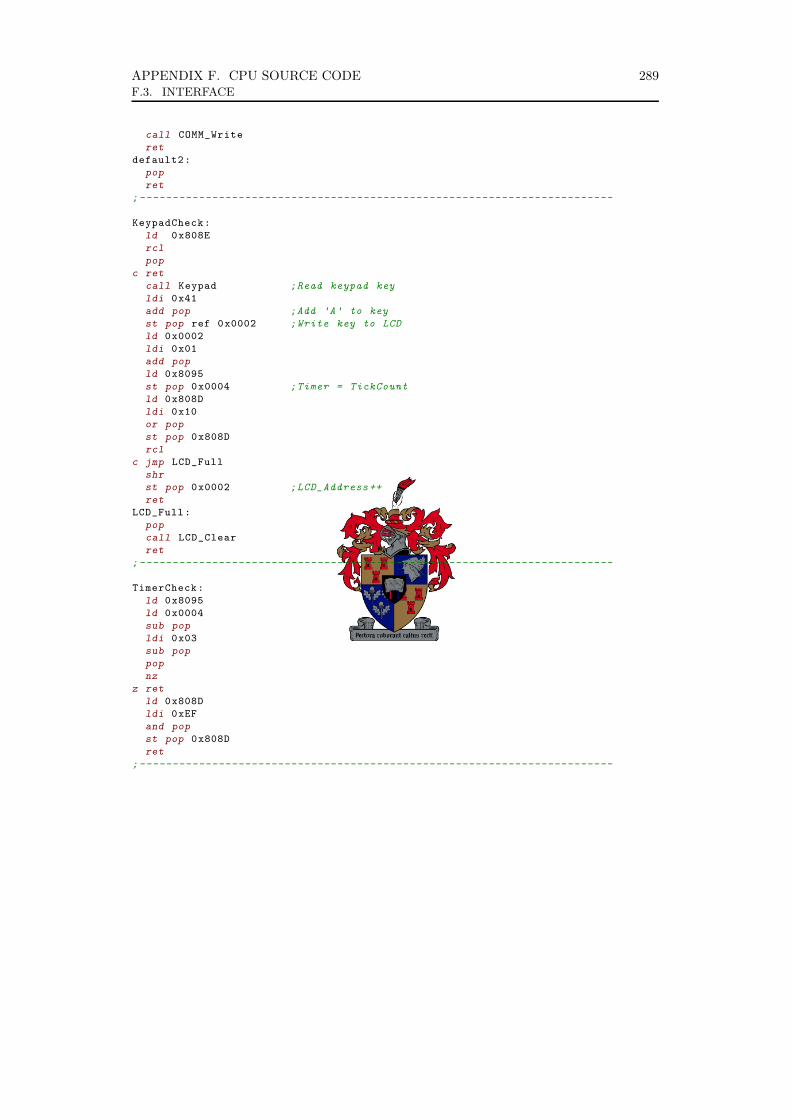
APPENDIX F. CPU SOURCE CODE 289F.3. INTERFACE
call COMM_Write
ret
default2:
pop
ret
;------------------------------------------------------------------------
KeypadCheck:
ld 0x808E
rcl
pop
c ret
call Keypad ;Read keypad key
ldi 0x41
add pop ;Add 'A' to key
st pop ref 0x0002 ;Write key to LCD
ld 0x0002
ldi 0x01
add pop
ld 0x8095
st pop 0x0004 ;Timer = TickCount
ld 0x808D
ldi 0x10
or pop
st pop 0x808D
rcl
c jmp LCD_Full
shr
st pop 0x0002 ;LCD_Address++
ret
LCD_Full:
pop
call LCD_Clear
ret
;------------------------------------------------------------------------
TimerCheck:
ld 0x8095
ld 0x0004
sub pop
ldi 0x03
sub pop
pop
nz
z ret
ld 0x808D
ldi 0xEF
and pop
st pop 0x808D
ret
;------------------------------------------------------------------------

Appendix G
Programmer Source Code
G.1 Introduction
The CPU programmer was programmed in Borland C++ Builder 4 and is fully-functional.This appendix presents the program code.
G.2 Graphical Interface
The programmer window is shown in figure G.1. The menus are shown in figure G.2.
290
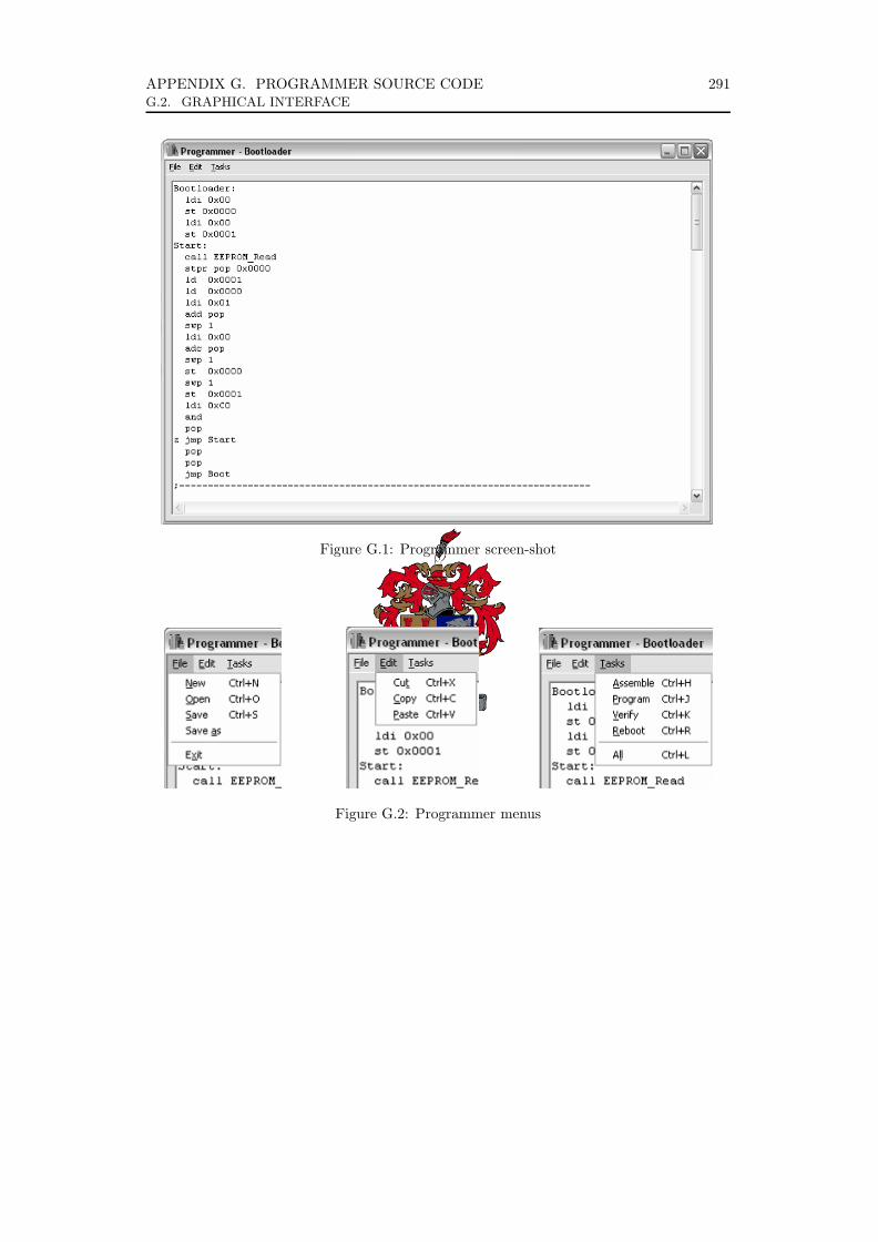
APPENDIX G. PROGRAMMER SOURCE CODE 291G.2. GRAPHICAL INTERFACE
Appendix G – Programmer Source Code : Introduction 262
Appendix G – Programmer Source Code
G.1 Introduction The CPU programmer was programmed in Borland C++ Builder 4 and is fully-functional. This
appendix presents the program code.
G.2 Graphical Interface The programmer window is shown in figure G.1. The menus are shown in figure G.2.
Figure G.1 – Programmer screen-shot
Figure G.2 – Programmer menus
Figure G.1: Programmer screen-shot
Appendix G – Programmer Source Code : Introduction 262
Appendix G – Programmer Source Code
G.1 Introduction The CPU programmer was programmed in Borland C++ Builder 4 and is fully-functional. This
appendix presents the program code.
G.2 Graphical Interface The programmer window is shown in figure G.1. The menus are shown in figure G.2.
Figure G.1 – Programmer screen-shot
Figure G.2 – Programmer menus Figure G.2: Programmer menus

APPENDIX G. PROGRAMMER SOURCE CODE 292G.3. PROGRAMMER
G.3 Programmer
G.3.1 Body
// ---------------------------------------------------------------------------
#include <vcl.h>
#pragma hdrstop
USERES("Programmer.res");
USEFORM("FrmProgrammer.cpp", Prog);
USEUNIT("..\..\..\..\ Shared\Cpp\File\JFile.cpp");
USEUNIT("..\..\..\..\ Shared\Cpp\Comm\JComm.cpp");
USEUNIT("Assembler.cpp");
// ---------------------------------------------------------------------------
WINAPI WinMain(HINSTANCE , HINSTANCE , LPSTR , int)
try
Application ->Initialize();
Application ->CreateForm(__classid(TProg), &Prog);
Application ->Run();
catch (Exception &exception)
Application ->ShowException(&exception);
return 0;
// ---------------------------------------------------------------------------
G.4 Programmer Form
G.4.1 Header
// ---------------------------------------------------------------------------
#ifndef FrmProgrammerH
#define FrmProgrammerH
// ---------------------------------------------------------------------------
#include <Classes.hpp>
#include <Controls.hpp>
#include <StdCtrls.hpp>
#include <Forms.hpp>
#include <clipbrd.hpp>
#include <Menus.hpp>
#include <Dialogs.hpp>
// ---------------------------------------------------------------------------
#include "JFile.h"
#include "JComm.h"
#include "Assembler.h"
// ---------------------------------------------------------------------------
class TProg : public TForm
__published: // IDE -managed Components
TMemo *Asm;
TMainMenu *MainMenu1;
TMenuItem *File1;
TMenuItem *Edit1;
TMenuItem *Tasks1;
TMenuItem *New1;
TMenuItem *Open1;
TMenuItem *Save1;
TMenuItem *Saveas1;

APPENDIX G. PROGRAMMER SOURCE CODE 293G.4. PROGRAMMER FORM
TMenuItem *N1;
TMenuItem *Exit1;
TMenuItem *Cut1;
TMenuItem *Copy1;
TMenuItem *Paste1;
TMenuItem *Assemble1;
TMenuItem *Program1;
TMenuItem *Verify1;
TMenuItem *N2;
TMenuItem *All1;
TOpenDialog *OpenDialog;
TSaveDialog *SaveDialog;
TMenuItem *Reboot1;
void __fastcall FormResize(TObject *Sender);
void __fastcall New1Click(TObject *Sender);
void __fastcall Open1Click(TObject *Sender);
void __fastcall Save1Click(TObject *Sender);
void __fastcall Saveas1Click(TObject *Sender);
void __fastcall Exit1Click(TObject *Sender);
void __fastcall Cut1Click(TObject *Sender);
void __fastcall Copy1Click(TObject *Sender);
void __fastcall Paste1Click(TObject *Sender);
void __fastcall Assemble1Click(TObject *Sender);
void __fastcall Program1Click(TObject *Sender);
void __fastcall Verify1Click(TObject *Sender);
void __fastcall All1Click(TObject *Sender);
void __fastcall AsmChange(TObject *Sender);
void __fastcall FormClose(TObject *Sender , TCloseAction &Action);
void __fastcall Reboot1Click(TObject *Sender);
private: // User declarations
JFile File;
JComm Comm;
JAssembler Assembler;
bool Saved;
bool Success;
bool Messages;
AnsiString Path ; //Including the ending "/"
AnsiString Filename; //Only the name , not the extension
public: // User declarations
__fastcall TProg(TComponent* Owner);
;
// ---------------------------------------------------------------------------
extern PACKAGE TProg *Prog;
// ---------------------------------------------------------------------------
#endif
G.4.2 Body
// ---------------------------------------------------------------------------
#include <vcl.h>
#pragma hdrstop
#include "FrmProgrammer.h"
// ---------------------------------------------------------------------------
#pragma package(smart_init)
#pragma resource "*.dfm"
TProg *Prog;
// ---------------------------------------------------------------------------
__fastcall TProg::TProg(TComponent* Owner)
: TForm(Owner)
Saved = true;

APPENDIX G. PROGRAMMER SOURCE CODE 294G.4. PROGRAMMER FORM
Path = "";
Filename = "";
Caption = "Programmer - [Untitled]";
Messages = true;
// ---------------------------------------------------------------------------
void __fastcall TProg::FormResize(TObject *Sender)
Asm->Width = ClientWidth - 16;
Asm->Height = ClientHeight - 16;
// ---------------------------------------------------------------------------
void __fastcall TProg::New1Click(TObject *Sender)
if(!Saved)
switch(Application ->MessageBox("Would you like to save first",
"Not saved",
MB_ICONQUESTION | MB_YESNOCANCEL))
case IDYES:
Save1Click(this);
case IDNO:
break;
default:
return;
Saved = true;
Path = "";
Filename = "";
Asm->Lines ->Clear();
Caption = "Programmer - [Untitled]";
// ---------------------------------------------------------------------------
void __fastcall TProg::Open1Click(TObject *Sender)
if(!Saved)
switch(Application ->MessageBox("Would you like to save first",
"Not saved",
MB_ICONQUESTION | MB_YESNOCANCEL))
case IDYES:
Save1Click(this);
case IDNO:
break;
default:
return;
if(!OpenDialog ->Execute()) return;
int j;
Filename = OpenDialog ->FileName;
for(j = Filename.Length(); Filename[j] != '\\'; j--);
Path = Filename.SubString(1, j);
Filename = Filename.SubString(j+1, Filename.Length()-j);
if(Filename.SubString(Filename.Length()-3, 4).UpperCase() == ".ASM")
Filename = Filename.SubString(1, Filename.Length()-4);
else
if(!CopyFile((Path + Filename).c_str(),
(Path + Filename + ".asm").c_str(), true))
Application ->MessageBox("Could not copy file to have a \".asm\" extention",
"Error",
MB_ICONERROR);
return;

APPENDIX G. PROGRAMMER SOURCE CODE 295G.4. PROGRAMMER FORM
File.FileName = Path + Filename + ".asm";
if(!File.Open(JFile::Read))
File.ShowLastError();
return;
if(File.Size)
char* c = new char[File.Size+1];
c[File.Size] = 0;
bool b;
if(!File.ReadBuffer(c, File.Size , b))
File.ShowLastError();
File.Close();
delete[] c;
return;
Asm->Lines ->Text = c;
delete[] c;
else
Asm->Lines ->Clear();
File.Close();
Saved = true;
Caption = "Programmer - " + Filename;
// ---------------------------------------------------------------------------
void __fastcall TProg::Save1Click(TObject *Sender)
if(!Path.Length() || !Filename.Length())
Saveas1Click(this);
return;
if(Saved) return;
File.FileName = Path + Filename + ".asm";
if(!File.Open(JFile::Create))
File.ShowLastError();
return;
if(Asm->Lines ->Text.Length())
bool b;
if(!File.WriteBuffer(Asm->Lines ->Text.c_str(),
Asm->Lines ->Text.Length(), b))
File.ShowLastError();
File.Close();
return;
File.Close();
Saved = true;
Caption = "Programmer - " + Filename;
// ---------------------------------------------------------------------------
void __fastcall TProg::Saveas1Click(TObject *Sender)
if(!SaveDialog ->Execute()) return;
int j;
Filename = SaveDialog ->FileName;
for(j = Filename.Length(); Filename[j] != '\\'; j--);
Path = Filename.SubString(1, j);
Filename = Filename.SubString(j+1, Filename.Length()-j);
if(Filename.SubString(Filename.Length()-3, 4).UpperCase() == ".ASM")
Filename = Filename.SubString(1, Filename.Length()-4);

APPENDIX G. PROGRAMMER SOURCE CODE 296G.4. PROGRAMMER FORM
Saved = false;
Save1Click(this);
// ---------------------------------------------------------------------------
void __fastcall TProg::Exit1Click(TObject *Sender)
if(!Saved)
switch(Application ->MessageBox("Would you like to save first",
"Not saved",
MB_ICONQUESTION | MB_YESNOCANCEL))
case IDYES:
Save1Click(this);
case IDNO:
break;
default:
return;
Application ->Terminate();
// ---------------------------------------------------------------------------
void __fastcall TProg::Cut1Click(TObject *Sender)
Clipboard()->AsText = Asm->SelText;
Asm->SelText = "";
// ---------------------------------------------------------------------------
void __fastcall TProg::Copy1Click(TObject *Sender)
Clipboard()->AsText = Asm->SelText;
// ---------------------------------------------------------------------------
void __fastcall TProg::Paste1Click(TObject *Sender)
Asm->SelText = Clipboard()->AsText;
// ---------------------------------------------------------------------------
void __fastcall TProg::Assemble1Click(TObject *Sender)
Success = false;
Save1Click(this);
union
struct
unsigned __int8 lsb;
unsigned __int8 msb;
;
unsigned __int16 i;
;
int Size;
bool b;
AnsiString s;
int j;
char* Code = Assembler.Assemble(Asm->Lines ->Text.c_str(), Size);
if(!Code)
Asm->SelStart = Size;
Asm->SelLength = 0;
return;
File.FileName = Path + Filename + ".bin";

APPENDIX G. PROGRAMMER SOURCE CODE 297G.4. PROGRAMMER FORM
if(!File.Open(JFile::Create))
File.ShowLastError();
delete[] Code;
return;
if(!File.WriteBuffer(Code , Size , b))
File.ShowLastError();
delete[] Code;
File.Close();
return;
File.Close();
File.FileName = Path + Filename + ".hex";
if(!File.Open(JFile::Create))
File.ShowLastError();
delete[] Code;
return;
for(j = 0; j < Size; j++)
s = ":01"; //One byte in data
s += IntToHex(j, 4); //Starting address of data
s += "00"; //Data type
s += IntToHex((unsigned __int8)Code[j] , 2); //The actual data
i = j;
s += IntToHex((unsigned __int8)(~(lsb+msb+1+Code[j])+1), 2); //Checksum
s += "\r\n";
if(!File.WriteBuffer(s.c_str(), 15, b))
File.ShowLastError();
delete[] Code;
File.Close();
return;
if(!File.WriteBuffer(":00000001FF", 11, b))
File.ShowLastError();
delete[] Code;
File.Close();
return;
File.Close();
delete[] Code;
if(Messages)
Application ->MessageBox("Assembly complete",
"Complete",
MB_ICONINFORMATION);
Success = true;
// ---------------------------------------------------------------------------
void __fastcall TProg::Program1Click(TObject *Sender)
Success = false;
Save1Click(this);
union
struct
unsigned __int8 lsb;
unsigned __int8 msb;
;
unsigned __int16 i;
;
char* Data;
char Ack;
bool b;
int j;
APPENDIX G. PROGRAMMER SOURCE CODE 298G.4. PROGRAMMER FORM
int l;
if(!Comm.Open("COM1", CBR_115200 , 1000))
File.ShowLastError();
return;
File.FileName = Path + Filename + ".bin";
if(!File.Open(JFile::Read))
File.ShowLastError();
Comm.Close();
return;
l = File.Size;
if(l > 0x4000)
Application ->MessageBox("File too large",
"Error",
MB_ICONERROR);
File.Close();
Comm.Close();
return;
Data = new char[l];
if(!File.ReadBuffer(Data , l, b))
File.ShowLastError();
delete[] Data;
File.Close();
Comm.Close();
return;
File.Close();
for(j = 0; j < l; j++)
i = j;
if(!Comm.Write(0x01)) //Command for Write EEPROM
delete[] Data;
Comm.Close();
return;
if(!Comm.Write(lsb)) //lsb of Address
delete[] Data;
Comm.Close();
return;
if(!Comm.Write(msb)) //msb of Address
delete[] Data;
Comm.Close();
return;
if(!Comm.Write(Data[j])) //Data to be written
delete[] Data;
Comm.Close();
return;
if(!Comm.Read(Ack))
delete[] Data;
Comm.Close();
return;
delete[] Data;
Comm.Close();
if(Messages)
Application ->MessageBox("Programming complete",
"Complete",
MB_ICONINFORMATION);
Success = true;
APPENDIX G. PROGRAMMER SOURCE CODE 299G.4. PROGRAMMER FORM
// ---------------------------------------------------------------------------
void __fastcall TProg::Verify1Click(TObject *Sender)
Success = false;
Save1Click(this);
union
struct
unsigned __int8 lsb;
unsigned __int8 msb;
;
unsigned __int16 i;
;
char* Data;
char Ack;
bool b;
int j;
int l;
if(!Comm.Open("COM1", CBR_115200 , 1000))
File.ShowLastError();
return;
File.FileName = Path + Filename + ".bin";
if(!File.Open(JFile::Read))
File.ShowLastError();
Comm.Close();
return;
l = File.Size;
Data = new char[l];
if(!File.ReadBuffer(Data , l, b))
File.ShowLastError();
delete[] Data;
File.Close();
Comm.Close();
return;
File.Close();
for(j = 0; j < l; j++)
i = j;
if(!Comm.Write(0x02)) //Command for Read EEPROM
delete[] Data;
Comm.Close();
return;
if(!Comm.Write(lsb)) //lsb of Address
delete[] Data;
Comm.Close();
return;
if(!Comm.Write(msb)) //msb of Address
delete[] Data;
Comm.Close();
return;
if(!Comm.Read(Ack))
delete[] Data;
Comm.Close();
return;
if(Ack != Data[j])
Application ->MessageBox("Veryfication failed",
"Error",
MB_ICONERROR);

APPENDIX G. PROGRAMMER SOURCE CODE 300G.4. PROGRAMMER FORM
delete[] Data;
Comm.Close();
return;
delete[] Data;
Comm.Close();
if(Messages)
Application ->MessageBox("Veryfication complete",
"Complete",
MB_ICONINFORMATION);
Success = true;
// ---------------------------------------------------------------------------
void __fastcall TProg::Reboot1Click(TObject *Sender)
Success = false;
if(!Comm.Open("COM1", CBR_115200 , 1000))
File.ShowLastError();
return;
if(!Comm.Write(0x03)) //Command for reboot
Comm.Close();
return;
Comm.Close();
if(Messages)
Application ->MessageBox("Reboot complete",
"Complete",
MB_ICONINFORMATION);
Success = true;
// ---------------------------------------------------------------------------
void __fastcall TProg::All1Click(TObject *Sender)
Messages = false;
Assemble1Click(this);
if(!Success)
Messages = true;
return;
Program1Click(this);
if(!Success)
Messages = true;
return;
Verify1Click(this);
if(!Success)
Messages = true;
return;
Reboot1Click(this);
Messages = true;
Application ->MessageBox("All operations complete",
"Complete",
MB_ICONINFORMATION);
// ---------------------------------------------------------------------------
void __fastcall TProg::AsmChange(TObject *Sender)

APPENDIX G. PROGRAMMER SOURCE CODE 301G.5. ASSEMBLER
Saved = false;
// ---------------------------------------------------------------------------
void __fastcall TProg::FormClose(TObject *Sender , TCloseAction &Action)
Action = caNone;
Exit1Click(this);
// ---------------------------------------------------------------------------
G.5 Assembler
G.5.1 Header
// ---------------------------------------------------------------------------
#ifndef AssemblerH
#define AssemblerH
// ---------------------------------------------------------------------------
#include <Forms.hpp>
#include <system.hpp>
// ---------------------------------------------------------------------------
class JAssembler
private:
enum
Label = 0x81,
LabelRef = 0x82,
Number = 0x83,
Sref = 0x84,
Sval = 0x85,
Sline = 0x86,
Send = 0x87,
Sc = 0x80,
Sz = 0x40,
Sc_z = 0xC0, //"c&z"
Sadc = 0x00,
Sadd = 0x02,
Sand = 0x04,
Sdiv = 0x06,
Smul = 0x08,
Sneg = 0x0A,
Snot = 0x0B,
Sor = 0x0C,
Ssbb = 0x0E,
Ssub = 0x10,
Sxor = 0x12,
Srcl = 0x14,
Srcr = 0x15,
Srol = 0x16,
Sror = 0x17,
Sshl = 0x18,
Sshr = 0x19,
Scc = 0x1A,
Scz = 0x1B,
Snc = 0x1C,
Snz = 0x1D,
Ssc = 0x1E,
Ssz = 0x1F,
Sswp = 0x20,
Spop = 0x28,
Sret = 0x29,

APPENDIX G. PROGRAMMER SOURCE CODE 302G.5. ASSEMBLER
Scall = 0x2A,
Sjmp = 0x2C,
Sld = 0x2E,
Slds = 0x30,
Sldi = 0x38,
Sldpr = 0x39,
Sstpr = 0x3A,
Sst = 0x3C
Sym;
struct JUMP
int Address;
int Character;
AnsiString Label;
JUMP* Next;
;
JUMP* Labels;
JUMP* Jumps;
char* Data;
unsigned __int8* Code;
int DataCount;
int CodeCount;
int CodeSize;
unsigned __int16 I;
AnsiString S;
bool ErrorSet;
void Error(char* s);
void Larger(void);
void Put(unsigned __int8 c);
void Get(void);
unsigned __int16 Val(char* s);
unsigned __int16 ValHex(char* s);
void Line(void);
void Opcode(unsigned __int8 c);
void SolveJumps(void);
void Cleanup(void);
public:
JAssembler(void);
char* Assemble(char* Asm, int& Size); //Size = 0 => Error
;
// ---------------------------------------------------------------------------
#endif
G.5.2 Body
/*Do error handling - quit on error*/
#include "Assembler.h"
#include <stdlib.h>
// ---------------------------------------------------------------------------
JAssembler::JAssembler(void)
Jumps = 0;
Labels = 0;
// ---------------------------------------------------------------------------
void JAssembler::Larger(void)
unsigned __int8* c = new unsigned __int8[CodeSize << 1];
for(int j = 0; j < CodeSize; j++)
c[j] = Code[j];
CodeSize <<= 1;
delete[] Code;
Code = c;

APPENDIX G. PROGRAMMER SOURCE CODE 303G.5. ASSEMBLER
// ---------------------------------------------------------------------------
void JAssembler::Put(unsigned __int8 c)
if(ErrorSet) return;
if(CodeCount == CodeSize) Larger();
Code[CodeCount++] = c;
// ---------------------------------------------------------------------------
void JAssembler::Error(char* s)
if(ErrorSet) return;
ErrorSet = true;
Application ->MessageBox(s, "Error", MB_ICONERROR);
// ---------------------------------------------------------------------------
char* JAssembler::Assemble(char* Asm, int& Size)
ErrorSet = false;
Data = Asm;
DataCount = 0;
CodeCount = 0;
Code = new unsigned __int8[2];
CodeSize = 2;
Get();
Line();
Size = CodeCount;
if(ErrorSet)
Size = DataCount;
Cleanup();
delete[] Code;
Code = 0;
return (char*)Code;
// ---------------------------------------------------------------------------
unsigned __int16 JAssembler::Val(char* s)
if(ErrorSet) return 0;
unsigned __int16 i = 0;
int j = 0;
while(s[j])
if(s[j] >= '0' && s[j] <= '9')i *= (unsigned __int16)10;
i += (unsigned __int16)s[j] - (unsigned __int16)'0';else
Error("Illigal character in number");
return 0;
j++;
return i;
// ---------------------------------------------------------------------------
unsigned __int16 JAssembler::ValHex(char* s)
if(ErrorSet) return 0;
unsigned __int16 i = 0;
int j = 0;
while(s[j])
i *= (unsigned __int16)16;
if(s[j] >= '0' && s[j] <= '9')i += (unsigned __int16)s[j] - (unsigned __int16)'0';
else if(s[j] >= 'A' && s[j] <= 'F')i += (unsigned __int16)s[j] - (unsigned __int16)'A';
APPENDIX G. PROGRAMMER SOURCE CODE 304G.5. ASSEMBLER
i += (unsigned __int16)10;
else if(s[j] >= 'a' && s[j] <= 'f')i += (unsigned __int16)s[j] - (unsigned __int16)'a';i += (unsigned __int16)10;
else
Error("Illigal character in number");
return 0;
j++;
return i;
// ---------------------------------------------------------------------------
void JAssembler::Get(void)
if(ErrorSet) return;
while(Data[DataCount] == ' ') DataCount++;
AnsiString s = "";
while(Data[DataCount] != ' ' &&
Data[DataCount] != ';' &&
Data[DataCount] != '\n' &&
Data[DataCount] != '\r' &&
Data[DataCount] != 0 )
s += Data[DataCount++];
if(s == "")
if(Data[DataCount] == ';')while(Data[DataCount] != '\n' &&
Data[DataCount] != '\r' &&
Data[DataCount] != 0 )
DataCount++;
if(Data[DataCount] == 0)
Sym = Send;
else
Sym = Sline;
while(Data[DataCount] == '\n' ||
Data[DataCount] == '\r' )
DataCount++;
else if(s == "adc")
Sym = Sadc;
else if(s == "add")
Sym = Sadd;
else if(s == "and")
Sym = Sand;
else if(s == "div")
Sym = Sdiv;
else if(s == "mul")
Sym = Smul;
else if(s == "neg")
Sym = Sneg;
else if(s == "not")
Sym = Snot;
else if(s == "or")
Sym = Sor;
else if(s == "sbb")
Sym = Ssbb;
else if(s == "sub")
Sym = Ssub;
else if(s == "xor")
Sym = Sxor;
else if(s == "rcl")

APPENDIX G. PROGRAMMER SOURCE CODE 305G.5. ASSEMBLER
Sym = Srcl;
else if(s == "rcr")
Sym = Srcr;
else if(s == "rol")
Sym = Srol;
else if(s == "ror")
Sym = Sror;
else if(s == "shl")
Sym = Sshl;
else if(s == "shr")
Sym = Sshr;
else if(s == "cc")
Sym = Scc;
else if(s == "cz")
Sym = Scz;
else if(s == "nc")
Sym = Snc;
else if(s == "nz")
Sym = Snz;
else if(s == "sc")
Sym = Ssc;
else if(s == "sz")
Sym = Ssz;
else if(s == "swp")
Sym = Sswp;
else if(s == "pop")
Sym = Spop;
else if(s == "ret")
Sym = Sret;
else if(s == "call")
Sym = Scall;
else if(s == "jmp")
Sym = Sjmp;
else if(s == "ld")
Sym = Sld;
else if(s == "lds")
Sym = Slds;
else if(s == "ldi")
Sym = Sldi;
else if(s == "ldpr")
Sym = Sldpr;
else if(s == "stpr")
Sym = Sstpr;
else if(s == "st")
Sym = Sst;
else if(s == "c")
Sym = Sc;
else if(s == "z")
Sym = Sz;
else if(s == "z&c")
Sym = Sc_z;
else if(s == "c&z")
Sym = Sc_z;
else if(s == "ref")
Sym = Sref;
else if(s == "val")
Sym = Sval;
else if(s[s.Length()] == ':') //Label
Sym = Label;
S = s.SubString(1, s.Length()-1);
else if(s.SubString(1, 2).UpperCase() == "0X") //Hexadecimal
Sym = Number;
I = ValHex(s.SubString(3, s.Length()-2).c_str());
else if(s[1] >= '0' && s[1] <= '9') //Decimal
Sym = Number;
APPENDIX G. PROGRAMMER SOURCE CODE 306G.5. ASSEMBLER
I = Val(s.c_str());
else //Label reference
Sym = LabelRef;
S = s;
// ---------------------------------------------------------------------------
void JAssembler::SolveJumps(void)
if(ErrorSet) return;
union
struct
unsigned __int8 lsb;
unsigned __int8 msb;
;
unsigned __int16 i;
;
JUMP* Label;
JUMP* Jump;
JUMP* Temp;
int j;
Jump = Jumps;
while(Jump)
Label = Labels;
while(Label && Label ->Label != Jump ->Label) Label = Label ->Next;
if(!Label)
DataCount = Jump ->Character;
Error("Label not found");
return;
if(abs(Label ->Address - Jump ->Address) <= 0x7F)
Temp = Labels;
while(Temp ->Address > Jump ->Address)
Temp ->Address --;
Temp = Temp ->Next;
Temp = Jumps;
while(Temp ->Address > Jump ->Address)
Temp ->Address --;
Temp = Temp ->Next;
j = Jump ->Address+2;
while(j < CodeCount -1)
Code[j] = Code[j+1];
j++;
CodeCount --;
else
Code[Jump ->Address]++;
Jump = Jump ->Next;
while(Jumps)
Label = Labels;
while(Label && Label ->Label != Jumps ->Label) Label = Label ->Next;
if(Code[Jumps ->Address] & 0x01)
i = Label ->Address;
Code[Jumps ->Address+1] = lsb;
Code[Jumps ->Address+2] = msb;
else
Code[Jumps ->Address+1] = Label ->Address - Jumps ->Address;
Temp = Jumps;
Jumps = Jumps ->Next;
delete Temp;

APPENDIX G. PROGRAMMER SOURCE CODE 307G.5. ASSEMBLER
while(Labels)
Temp = Labels;
Labels = Labels ->Next;
delete Temp;
// ---------------------------------------------------------------------------
void JAssembler::Line(void)
JUMP* Temp;
unsigned __int8 c;
while(!ErrorSet && Sym != Send)
c = 0x00;
while(Sym == Sline) Get();
if(Sym == Label)
Temp = Labels;
while(Temp)
if(Temp ->Label == S)
Error("Duplicate lable");
return;
Temp = Temp ->Next;
Temp = new JUMP;
Temp ->Address = CodeCount;
Temp ->Label = S;
Temp ->Next = Labels;
Labels = Temp;
Get();
while(Sym == Sline) Get();
if(Sym == Sc ||
Sym == Sz ||
Sym == Sc_z)
c = Sym;
Get();
Opcode(c);
SolveJumps();
// ---------------------------------------------------------------------------
void JAssembler::Opcode(unsigned __int8 c)
if(ErrorSet) return;
union
struct
unsigned __int8 lsb;
unsigned __int8 msb;
;
unsigned __int16 i;
;
JUMP* Temp;
switch(Sym)
case Sadc:
case Sadd:
case Sand:
case Sdiv:
case Smul:
case Sor:
case Ssbb:
case Ssub:
case Sxor:
c += Sym;

APPENDIX G. PROGRAMMER SOURCE CODE 308G.5. ASSEMBLER
Get();
if(Sym == Spop)
Put(c+(unsigned __int8)1);
Get();
else
Put(c);
break;
case Sneg:
case Snot:
case Srcl:
case Srcr:
case Srol:
case Sror:
case Sshl:
case Sshr:
case Scc:
case Scz:
case Snc:
case Snz:
case Ssc:
case Ssz:
case Spop:
case Sret:
Put(c+(unsigned __int8)Sym);
Get();
break;
case Sswp:
case Slds:
c += Sym;
Get();
if(Sym == Number && I <= 7)
Put(c+(unsigned __int8)I);
else
Error("Expected number");
return;
Get();
break;
case Scall:
case Sjmp:
Put(c+(unsigned __int8)Sym);
Get();
if(Sym == LabelRef)
Temp = new JUMP;
Temp ->Address = CodeCount -1;
Temp ->Label = S;
Temp ->Character = DataCount;
Temp ->Next = Jumps;
Jumps = Temp;
Put(0x00);
Put(0x00);
else
Error("Expected label");
return;
Get();
break;
case Sld:
c += Sym;
Get();
if(Sym == Sref)
c++;
Get();
else if(Sym == Sval)
APPENDIX G. PROGRAMMER SOURCE CODE 309G.5. ASSEMBLER
Get();
Put(c);
if(Sym == Number)
i = I;
Put(lsb);
Put(msb);
else
Error("Expected number");
return;
Get();
break;
case Sldi:
Put(c+(unsigned __int8)Sym);
Get();
if(Sym == Number)
Put(I);
else
Error("Expected number");
return;
Get();
break;
case Sldpr:
Put(c+(unsigned __int8)Sym);
Get();
if(Sym == Number)
i = I;
Put(lsb);
Put(msb);
else
Error("Expected number");
return;
Get();
break;
case Sstpr:
c += Sym;
Get();
if(Sym == Spop)
Put(c+(unsigned __int8)1);
Get();
else
Put(c);
if(Sym == Number)
i = I;
Put(lsb);
Put(msb);
else
Error("Expected number");
return;
Get();
break;
case Sst:
c += Sym;
Get();
if(Sym == Spop)
c += (unsigned __int8)2;
Get();
if(Sym == Sref)
c++;

APPENDIX G. PROGRAMMER SOURCE CODE 310G.6. JCOMM
Get();
else if(Sym == Sval)
Get();
Put(c);
if(Sym == Number)
i = I;
Put(lsb);
Put(msb);
else
Error("Expected number");
return;
Get();
break;
case Label:
case Sline:
case Send:
break;
default:
Error("Expected opcode");
break;
// ---------------------------------------------------------------------------
void JAssembler::Cleanup(void)
JUMP* Temp;
while(Jumps)
Temp = Jumps;
Jumps = Jumps ->Next;
delete Temp;
while(Labels)
Temp = Labels;
Labels = Labels ->Next;
delete Temp;
// ---------------------------------------------------------------------------
G.6 JComm
Components ‘JComm’ and ‘JFile’ were developed for prior projects and is not included inthe development time.
G.6.1 Header
// ---------------------------------------------------------------------------
#ifndef JCommH
#define JCommH
// ---------------------------------------------------------------------------
#include <system.hpp>
// ---------------------------------------------------------------------------
class JComm
private:
HANDLE Handle;
public:
JComm(void);
~JComm(void);

APPENDIX G. PROGRAMMER SOURCE CODE 311G.6. JCOMM
bool Open(char* Port , int Baud , int TimeOut);
bool Read(char& c);
bool Write(char c);
void Close(void);
;
// ---------------------------------------------------------------------------
#endif
G.6.2 Body
// ---------------------------------------------------------------------------
#include <vcl.h>
#pragma hdrstop
#include "JComm.h"
// ---------------------------------------------------------------------------
#pragma package(smart_init)
JComm::JComm(void)
Handle = 0;
// ---------------------------------------------------------------------------
JComm::~JComm(void)
Close();
// ---------------------------------------------------------------------------
bool JComm::Open(char* Port , int Baud , int TimeOut)
DCB dcb;
COMMTIMEOUTS cto;
Handle = CreateFile(Port ,
GENERIC_READ | GENERIC_WRITE ,
0, /* comm devices must be opened w/exclusive -access */
NULL , /* no security attrs */
OPEN_EXISTING , /* comm devices must use OPEN_EXISTING */
0, /* not overlapped I/O */
NULL); /* hTemplate must be NULL for comm devices */
if(Handle == INVALID_HANDLE_VALUE) return false;
if(!GetCommState(Handle , &dcb))
CloseHandle(Handle);
return false;
dcb.BaudRate = Baud;
dcb.ByteSize = 8;
dcb.Parity = NOPARITY;
dcb.StopBits = ONESTOPBIT;
if(!SetCommState(Handle , &dcb))
CloseHandle(Handle);
return false;
cto.ReadIntervalTimeout = TimeOut;
cto.ReadTotalTimeoutMultiplier = TimeOut;
cto.ReadTotalTimeoutConstant = 0;
cto.WriteTotalTimeoutMultiplier = TimeOut;
cto.WriteTotalTimeoutConstant = 0;
if(!SetCommTimeouts(Handle , &cto))
CloseHandle(Handle);
return false;
return true;
// ---------------------------------------------------------------------------
APPENDIX G. PROGRAMMER SOURCE CODE 312G.7. JFILE
bool JComm::Read(char& c)
unsigned long l;
ReadFile(Handle , &c, 1, &l, 0);
if(l == 0)
return false;
return true;
// ---------------------------------------------------------------------------
bool JComm::Write(char c)
unsigned long l;
WriteFile(Handle , &c, 1, &l, 0);
if(l == 0)
return false;
return true;
// ---------------------------------------------------------------------------
void JComm::Close(void)
if(Handle) CloseHandle(Handle);
Handle = 0;
// ---------------------------------------------------------------------------
G.7 JFile
Components ‘JComm’ and ‘JFile’ were developed for prior projects and is not included inthe development time.
G.7.1 Header
// ---------------------------------------------------------------------------
#ifndef JFileH
#define JFileH
// ---------------------------------------------------------------------------
class JFile
public:
enum ACCESS
Read = 0,
Write = 1,
Create = 2
;
private:
#include "winbase.h"
// ---------------------------------------------------------------------------
ACCESS CurrentAccess;
void* Handle;
char* Filename;
_OFSTRUCT* OpenBuffer;
// ---------------------------------------------------------------------------
bool LInput(AnsiString& s);
bool LPrint(AnsiString s);
void Copy(char* to, char* from);
// ---------------------------------------------------------------------------
AnsiString GetFileName(void);
void SetFileName(AnsiString Value);
unsigned long GetSize(void);
unsigned long GetPosition(void);

APPENDIX G. PROGRAMMER SOURCE CODE 313G.7. JFILE
void SetPosition(unsigned long Value);
bool GetBusy(void);
public:
struct ERRErr;
JFile (void);
~JFile (void);
void ShowLastError(void);
bool Open (ACCESS Access);
AnsiString ReadLine (bool& Value);
bool WriteLine (AnsiString Value);
unsigned long ReadBuffer (char* Buffer , unsigned long MustRead ,
bool& Value);
unsigned long WriteBuffer (char* Buffer , unsigned long MustWrite ,
bool& Value);
void Close (void);
// ---------------------------------------------------------------------------
__property AnsiString FileName = read=GetFileName ,
write=SetFileName;
__property unsigned long Size = read=GetSize;
__property unsigned long Position = read=GetPosition ,
write=SetPosition;
__property bool Busy = read=GetBusy;
__fastcall JFile(TComponent* Owner);
;
// ---------------------------------------------------------------------------
#endif
G.7.2 Body
// ---------------------------------------------------------------------------
#include <vcl.h>
#pragma hdrstop
#include "JFile.h"
#pragma package(smart_init)
// ---------------------------------------------------------------------------
JFile::JFile()
try
Filename = new char[0xFFFF];
catch(...)
Application ->MessageBox ("Out of memory.", "Error", MB_ICONERROR);
Application ->Terminate();
Filename[0] = (char)0;
Handle = 0;
OpenBuffer = new _OFSTRUCT;
CurrentAccess = Read;
// ---------------------------------------------------------------------------
bool JFile::LInput(AnsiString& s)
unsigned long X;
char x[2];
s = "";
if (!ReadFile(Handle , x, 1, &X, 0)) return false;
if (X <= 0) return false;
x[1] = x[0];
while(true)
if (!ReadFile(Handle , x, 1, &X, 0)) return true;
if (X <= 0)
s += x[1];
return true;

APPENDIX G. PROGRAMMER SOURCE CODE 314G.7. JFILE
if (((int)x[1] == 13 && (int)x[0] == 10) || // return + line feed
(int)x[1] == 10 || // line feed
(int)x[1] == 26) return true; // end of file
s += x[1];
x[1] = x[0];
// ---------------------------------------------------------------------------
bool JFile::LPrint(AnsiString s)
unsigned long X;
AnsiString x;
x = s + "\r\n";
return WriteFile(Handle , x.c_str(), x.Length(), &X, 0);
// ---------------------------------------------------------------------------
JFile::~JFile(void)
Close();
delete[] Filename;
// ---------------------------------------------------------------------------
void JFile::Close(void)
if (Handle)
CloseHandle(Handle);
Handle = 0;
// ---------------------------------------------------------------------------
bool JFile::Open(ACCESS Access)
Close();
switch (Access)
case Read: Handle = (void*)OpenFile(Filename , OpenBuffer ,
OF_READ);
if ((int)Handle < 1)
Handle = 0;
return false;
CurrentAccess = Read;
break;
case Write: Handle = (void*)OpenFile(Filename , OpenBuffer ,
OF_WRITE);
if ((int)Handle < 1)
Handle = 0;
return false;
unsigned long x;
SetFilePointer(Handle , GetFileSize(Handle , &x), 0,
FILE_BEGIN);
CurrentAccess = Write;
break;
case Create: Handle = (void*)OpenFile(Filename , OpenBuffer ,
OF_WRITE + OF_CREATE);
if ((int)Handle < 1)
Handle = 0;
return false;
CurrentAccess = Create;
break;
return true;
// ---------------------------------------------------------------------------
APPENDIX G. PROGRAMMER SOURCE CODE 315G.7. JFILE
void JFile::ShowLastError(void)
AnsiString A;
char Buffer[50];
FormatMessage((unsigned long)FORMAT_MESSAGE_FROM_SYSTEM ,
(const void*)FORMAT_MESSAGE_FROM_HMODULE ,
(unsigned long)GetLastError(),
(unsigned long)0,
(char*)Buffer ,
(unsigned long)50,
(const void*)"");
A = IntToStr(GetLastError()) + ": " + Buffer;
if (Application ->MessageBox(A.c_str(), "Error",
MB_ICONERROR + MB_OKCANCEL) == IDCANCEL)
Application ->Terminate();
// ---------------------------------------------------------------------------
void JFile::Copy(char* to, char* from)
for (int j = 0; (from[j-1] != (char)0 || j == 0); j++)
to[j] = from[j];
// ---------------------------------------------------------------------------
AnsiString JFile::GetFileName(void)
AnsiString t;
t = (AnsiString)Filename;
return t;
// ---------------------------------------------------------------------------
void JFile::SetFileName(AnsiString Value)
Close();
if(Value.Length() < 3)
Filename[0] = (char)0;
return;
if (Value[2] != ':' || Value[3] != '\\')AnsiString t;
t = "Invalid path and filename: ";
t += Value;
t += ".";
Application ->MessageBox (t.c_str(), "Error", MB_ICONERROR);
Filename[0] = (char)0;
return;
Copy(Filename , Value.c_str());
// ---------------------------------------------------------------------------
AnsiString JFile::ReadLine(bool& Value)
if (!CurrentAccess)
AnsiString Val;
Value = LInput(Val);
return Val;
else
Value = false;
return "";
// ---------------------------------------------------------------------------
bool JFile::WriteLine(AnsiString Value)

APPENDIX G. PROGRAMMER SOURCE CODE 316G.7. JFILE
if (CurrentAccess)
if (!LPrint(Value)) return false;
return true;
// ---------------------------------------------------------------------------
unsigned long JFile::ReadBuffer(char* Buffer , unsigned long MustRead ,
bool& Value)
unsigned long X = 0;
if (!CurrentAccess)
Value = ReadFile(Handle , Buffer , MustRead , &X, 0);
else
Value = false;
return X;
// ---------------------------------------------------------------------------
unsigned long JFile::WriteBuffer(char* Buffer , unsigned long MustWrite ,
bool& Value)
unsigned long X = 0;
if (CurrentAccess)
Value = WriteFile(Handle , Buffer , MustWrite , &X, 0);
else
Value = false;
return X;
// ---------------------------------------------------------------------------
unsigned long JFile::GetSize(void)
unsigned long x;
if(Handle) return GetFileSize(Handle , &x);
return 0;
// ---------------------------------------------------------------------------
unsigned long JFile::GetPosition(void)
if(Handle) return SetFilePointer(Handle , 0, 0, FILE_CURRENT);
return 0;
// ---------------------------------------------------------------------------
void JFile::SetPosition(unsigned long Value)
if(Handle) SetFilePointer(Handle , Value , 0, FILE_BEGIN);
// ---------------------------------------------------------------------------
bool JFile::GetBusy(void)
return (bool)Handle;
// ---------------------------------------------------------------------------
Appendix H
Simulation Source
H.1 Introduction
This appendix presents the simulation code used for the converter (MATLAB) and probe(C++) simulations.
H.2 Converter
H.2.1 Stage 1
%LC low -pass with R // R-L load , driven by switching between Vbus and Gnd
close all;
clear all;
format compact;
format short;
clc;
L1 = 3e-3;
RL = 50e-3;
C1 = 470e-6;
RC = 10e-3;
R1 = -22.5;
L2 = 60e-3;
R2 = 11.25;
Vbus = 535;
freq1 = 500;
freq2 = 5e3;
A = [(-L1-R1*RC*C1)/(L1*C1*(R1+RC)) (R1*L1-R1*RC*RL*C1)/(L1*C1*(R1+RC));
-1/L1 -RL/L1 ];
B = [Vbus*R1*RC/(L1*(R1+RC));
Vbus/L1 ];
C = [1 0];
D = 0;
e = 1/sqrt(2);
w = 2*pi*freq1;
P = [-e*w+sqrt((e^2-1)*w^2) -e*w-sqrt((e^2-1)*w^2)];
P = [-2*pi*freq1 -2*pi*freq2]; %more immune to bus -disturbance
317

APPENDIX H. SIMULATION SOURCE 318H.2. CONVERTER
K = -acker(A, B, P) %Included as a comparrison only
A = [(-R1*RC*L2*C1-R1*RC*L1*C1-L1*L2)/(L1*L2*C1*(R1+RC))
(R1*L1-R1*RC*RL*C1)/(L1*C1*(R1+RC))
(R1*R2*RC*C1-R1*L2)/(L2*C1*(R1+RC));
-1/L1 -RL/L1 0 ;
1/L2 0 -R2/L2 ];
B = [R1*RC*Vbus/(L1*(R1+RC));
Vbus/L1 ;
0 ];
C = [1 0 0];
Ci= [0 1 0];
D = 0;
P = [P -R2/L2];
K = acker(A, B, P);
K = -K
K = -K;
K(3) = 0;
N=[A B; C D]^ -1*[0;0;0;1];
N=N(4)+K*N(1:3);
sys=ss(A-B*K, B*N, C, D);
K1 = -K
KV1 = [' ' Binary(round (2^18/1024*300*K1(1)))]
KI1 = [' ' Binary(round (2^18/1024*15 *K1(2)))]
N1 = N
N1 = [' ' Binary(round (2^18/1024*300*N1))]
sys=ss(A-B*K, B*N, Ci, D);
sys=ss(A-B*K, B*N, C, D);
dt = 10e-12*2^21;
t = 0:dt:400e-3;
Q = length(t);
Vref = 1000*t.*(t < 375e-3) + 375*(t >= 375e-3);
x = [0; 0; 0];
y = C*x;
for j = 1:Q-1
dx = (A*x(:,j)+B*(-K*x(:,j) + N*Vref(j+1)))*dt;
x(:,j+1) = x(:,j) + dx;
y(j+1) = C*x(:,j+1);
end
figure; plot(t/1e-3, y);
figure; plot(t/1e-3, x(2,:));
Vref = 270;
x = ((A-B*K/Vbus*560)^-1)*(-B*N*Vref/Vbus*560);
y = C*x;
Q = 5000;
t = linspace(0, 4e-3, Q);
Vb = 485*(t < 2e-3) + 560*(t >= 2e-3);
dt = t(2) - t(1);
for j = 1:Q-1
dx = (A*x(:,j)+B*(-K*x(:,j) + N*Vref)/Vbus*Vb(j+1))*dt;
x(:,j+1) = x(:,j) + dx;
y(j+1) = C*x(:,j+1);
end
figure; plot(t/1e-3, y);
figure; plot(t/1e-3, x(2,:));
APPENDIX H. SIMULATION SOURCE 319H.2. CONVERTER
H.2.2 Stage 2
%LC low -pass with RL load , driven by input voltage
close all;
clear all;
format compact;
format short;
clc;
L1=200e-6;
RL1=50e-3;
C=470e-6;
RC=10e-3;
RL2=14.4;
L2=4;
A=[(-RC/L1-RC/L2) (RL2*RC/L2-1/C) (1/C-RL1*RC/L1);
1/L2 -RL2/L2 0 ;
-1/L1 0 -RL1/L1 ];
B=[RC/L1;
0 ;
1/L1 ];
C=[0 1 0 ];
D=0;
fast=11; % This is the 3 fast poles frequency
slow=1 ; % This is the closed loop frequency
e=1/2;
w=2*pi*fast;
P=[(-e+sqrt(e^2-1))*w; (-e-sqrt(e^2-1))*w; -w];
P_orig = eig(A)
P_moved = P
K=acker(A, B, P);
N=[A B; C D]^ -1*[0;0;0;1];
N=N(4)+K*N(1:3);
sys=ss(A-B*K, B*N, C, D);return;
K2 = -K
KV2 = [' ' Binary(round (2^18/240*240*K2(1)))]
KI2 = [' ' Binary(round (2^18/240*20 *K2(2)))]
KI3 = [' ' Binary(round (2^18/240*20 *K2(3)))]
N2 = N
N2 = [' ' Binary(round (2^18/240*20*N))]
ki = 0;
dk = 1;
Ci = [0 1 0 0];
busy = 1;
while busy == 1
ki = ki + dk;
Ai = [A-B*K B*N;
0 -ki 0 0];
Bi = [0;
0;
0;
ki];
sys = ss(Ai, Bi, Ci, 0);
p = eig(Ai);
p = p(4);
APPENDIX H. SIMULATION SOURCE 320H.2. CONVERTER
if dk == 1
if p < -2*pi*slow
dk = -0.1;
end;
elseif dk == -0.1
if p > -2*pi*slow
dk = 0.01;
end;
elseif dk == 0.01
if p < -2*pi*slow
dk = -0.001;
end;
elseif dk == -0.001
if p > -2*pi*slow
dk = 0.0001;
end;
elseif dk == 0.0001
if p <= -2*pi*slow
busy = 0;
end;
end;
end;
ki = ki
poles_int=eig(Ai)
L1=200e-6;
RL1=50e-3;
C=470e-6;
RC=10e-3;
RL2=14.4;
L2=15;
A=[(-RC/L1-RC/L2) (RL2*RC/L2-1/C) (1/C-RL1*RC/L1);
1/L2 -RL2/L2 0 ;
-1/L1 0 -RL1/L1 ];
B=[RC/L1;
0 ;
1/L1 ];
C=[0 1 0 ];
D=0;
Ai = [A-B*K B*N;
0 -ki 0 0];
Bi = [0;
0;
0;
ki];
Q = 2000;
% t = linspace(0, 0.25, Q); %For 4H
t = linspace(0, 0.6, Q); %For 15H
% t = linspace(0, 1, Q); %For 1H
ref = 1*(t >= 0);
x = [0; 0; 0];
dt = t(2) - t(1);
for j = 1:Q-1
dx = (A*x(:,j)+B*(-K*x(:,j) + N*ref(j+1)))*dt;
x(:,j+1) = x(:,j) + dx;
end
Fig(t, C*x, 'Time [s]', 'i_2 [A]', 40, [0 0.6 0 1.2]);
Q = 2000;
t = linspace(0, 1.6, Q);
ref = 1*(t >= 0);
x = [0; 0; 0; 0];
dt = t(2) - t(1);

APPENDIX H. SIMULATION SOURCE 321H.3. PROBE
for j = 1:Q-1
dx = (Ai*x(:,j)+Bi*ref(j+1))*dt;
x(:,j+1) = x(:,j) + dx;
end
Fig(t, Ci*x, 'Time [s]', 'i_2 [A]', 40, [0 1.6 0 1.2]);
P = 10000;
t = linspace(0, 15, P);
r = (5*t+1).*(t<=2.8) + 15.*(t>2.8 & t<=5) +
(-5*t + 40).*(t>5 & t<=7.8) + 1.*(t>7.8);
dt = t(2)-t(1);
I2 = 1;
V2 = I2*RL2;
I2 = I2;
I3 = I2;
u = I2;
x = [V2; I2; I3];
V3 = N*u - K*x;
e = r(1) - C*x;
for j = 2:P
x = [V2(j-1); I2(j-1); I3(j-1)];
e(j) = r(j)-C*x;
u(j) = u(j-1) + ki*e(j)*dt;
if u(j) < 0; u(j) = 0; end; %Integrator internal limit
V3(j) = N*u(j) - K*x;
if V3(j) < -1; V3(j) = -1; end; %Buck converter property (diode)
dx = (A*x + B*V3(j));
dx = dx*dt;
V2 (j) = V2 (j-1) + dx(1);
if V2(j) < -1; V2(j) = -1; end; %Clamping diode (load)
I2 (j) = I2 (j-1) + dx(2);
I3 (j) = I3 (j-1) + dx(3);
if I3(j) < 0; I3(j) = 0; end; %Buck converter (not synchronous buck)
end;
V1 = 1.25*V3;
V1 = V1.*(V1 >10) + 10*(V1 <=10);
D2 = V3./V1;
Fig(t, V2, 'Time [s]', 'v_2 [V]', 40, [0 15 -50 300]);
Fig(t, I2, 'Time [s]', 'i_2 [A]', 40, [0 15 -1 20]);
H.3 Probe
H.3.1 Header
// ---------------------------------------------------------------------------
#ifndef FrmBlockH
#define FrmBlockH
// ---------------------------------------------------------------------------
#include <Classes.hpp>
#include <Controls.hpp>
#include <StdCtrls.hpp>
#include <Forms.hpp>
#include "JFile.h"
// ---------------------------------------------------------------------------
class TBlockEq : public TForm
__published: // IDE -managed Components
void __fastcall FormClick(TObject *Sender);
private: // User declarations
JFile File;
class VECTOR

APPENDIX H. SIMULATION SOURCE 322H.3. PROBE
public:
double x;
double y;
double z;
VECTOR operator+ (VECTOR v);
VECTOR operator+ (double d);
VECTOR operator - (VECTOR v);
VECTOR operator - (double d);
VECTOR operator* (VECTOR v);
VECTOR operator* (double d);
VECTOR operator/ (double d);
void operator= (VECTOR v);
;
public: // User declarations
__fastcall TBlockEq(TComponent* Owner);
;
// ---------------------------------------------------------------------------
extern PACKAGE TBlockEq *BlockEq;
// ---------------------------------------------------------------------------
#endif
H.3.2 Body
#pragma inline
// ---------------------------------------------------------------------------
#include <vcl.h>
#pragma hdrstop
#include "FrmBlock.h"
#include "math.h"
#include "stdlib.h"
#include "dos.h"
// ---------------------------------------------------------------------------
#pragma package(smart_init)
#pragma resource "*.dfm"
TBlockEq *BlockEq;
// ---------------------------------------------------------------------------
__fastcall TBlockEq::TBlockEq(TComponent* Owner)
: TForm(Owner)
// ---------------------------------------------------------------------------
TBlockEq::VECTOR TBlockEq::VECTOR::operator+ (VECTOR v)
VECTOR ans;
ans.x = x + v.x;
ans.y = y + v.y;
ans.z = z + v.z;
return ans;
// ---------------------------------------------------------------------------
TBlockEq::VECTOR TBlockEq::VECTOR::operator+ (double d)
VECTOR ans;
ans.x = x + d;
ans.y = y + d;
ans.z = z + d;
return ans;
// ---------------------------------------------------------------------------
APPENDIX H. SIMULATION SOURCE 323H.3. PROBE
TBlockEq::VECTOR TBlockEq::VECTOR::operator - (VECTOR v)
VECTOR ans;
ans.x = x - v.x;
ans.y = y - v.y;
ans.z = z - v.z;
return ans;
// ---------------------------------------------------------------------------
TBlockEq::VECTOR TBlockEq::VECTOR::operator - (double d)
VECTOR ans;
ans.x = x - d;
ans.y = y - d;
ans.z = z - d;
return ans;
// ---------------------------------------------------------------------------
TBlockEq::VECTOR TBlockEq::VECTOR::operator* (VECTOR v)
VECTOR ans;
ans.x = (y * v.z) - (z * v.y);
ans.y = (z * v.x) - (x * v.z);
ans.z = (x * v.y) - (y * v.x);
return ans;
// ---------------------------------------------------------------------------
TBlockEq::VECTOR TBlockEq::VECTOR::operator* (double d)
VECTOR ans;
ans.x = x * d;
ans.y = y * d;
ans.z = z * d;
return ans;
// ---------------------------------------------------------------------------
TBlockEq::VECTOR TBlockEq::VECTOR::operator/ (double d)
VECTOR ans;
ans.x = x / d;
ans.y = y / d;
ans.z = z / d;
return ans;
// ---------------------------------------------------------------------------
void TBlockEq::VECTOR::operator= (VECTOR v)
x = v.x;
y = v.y;
z = v.z;
// ---------------------------------------------------------------------------
void __fastcall TBlockEq::FormClick(TObject *Sender)
Screen ->Cursor = crHourGlass;
//Constants
double pi = 3.14159265358979;
double a = 2*pi*10e3;
double G = 63025;
double g = 267.522128e6;
double Bx = 10e-6;//910e-12;
APPENDIX H. SIMULATION SOURCE 324H.3. PROBE
double T1 = 3.6;
double T2 = 4.7;
double a0 = 3.281003e-3;
double Limit = 0.05*a0; //The threshhold for pulses.
double tmax = 30;
int N = tmax*100e3;
double dt = 1./100e3;
//Variables
VECTOR B;
VECTOR f1;
VECTOR f2;
VECTOR f3;
VECTOR f4;
VECTOR temp;
VECTOR temp2;
int j;
//Vectors
double* t = new double[N];
double* B0 = new double[N];
double* w0 = new double[N];
double* M0 = new double[N];
VECTOR* M = new VECTOR[N];
double* wrf = new double[N];
double* phi = new double[N];
for(j = 0; j < N; j++)
t[j] = dt*j;
if(t[j] < 2.2)
B0[j] = 0.5*t[j] + 0.1;
else if(t[j] < 10)
B0[j] = 1.2;
else if(t[j] < 12.2)
B0[j] = -0.5*(t[j] - 10) + 1.2;
else
B0[j] = 0.1;
///*Temp*/B0[j] = 2*pi*50e6/g;/*Temp*/
w0[j] = -g*B0[j];
M0[j] = a0*B0[j];
M[0].x = 0.;
M[0].y = 164e-6;
M[0].z = M0[0];
wrf[0] = w0[0];
phi[0] = atan2(M[0].y, M[0].x) - pi/2;
a = G*(1+a*dt);
for(j = 0; j < N-1; j++)
phi[j+1] = atan2(M[j].y, M[j].x) - pi/2;
wrf[j+1] = wrf[j] + a*phi[j+1] - G*phi[j];
if(M[j].y < Limit*g*0.1/(-w0[j+1]))
B.x = Bx*g*0.1/(-w0[j+1]);
else
B.x = 0.;
B.y = -M[j].y*(496.1004265e-27 * w0[j+1]* w0[j+1])/(30e-3 +
(394.7841759e-21 * w0[j+1]* w0[j+1]));
APPENDIX H. SIMULATION SOURCE 325H.3. PROBE
B.z = (wrf[j+1]-w0[j+1])/g;
temp.x = M[j].x/T2;
temp.y = M[j].y/T2;
temp.z = (M[j].z - M0[j])/T1;
f1 = ((M[j]*B)*g - temp)*dt;
temp2 = M[j]+(f1/2.);
temp.x = temp2.x/T2;
temp.y = temp2.y/T2;
temp.z = (temp2.z - M0[j])/T1;
f2 = ((temp2*B)*g - temp)*dt;
temp2 = M[j]+(f2/2.);
temp.x = temp2.x/T2;
temp.y = temp2.y/T2;
temp.z = (temp2.z - M0[j])/T1;
f3 = ((temp2*B)*g - temp)*dt;
temp2 = M[j]+f3;
temp.x = temp2.x/T2;
temp.y = temp2.y/T2;
temp.z = (temp2.z - M0[j])/T1;
f4 = ((temp2*B)*g - temp)*dt;
M[j+1] = M[j] + (f1 + (f2*2.) + (f3*2.) + f4)/6.;
AnsiString s;
bool b;
File.FileName = "E:\\Buffer\\Data.txt";
if(File.Open(JFile::Create))
File.WriteLine("t w0 Mx My Mz phi wrf");
for(j = 0; j < N; j += N/1000)
s = FloatToStr(t[j]) + " ";
File.WriteBuffer(s.c_str(), s.Length(), b);
s = FloatToStr(w0[j]) + " ";
File.WriteBuffer(s.c_str(), s.Length(), b);
s = FloatToStr(M[j].x) + " ";
File.WriteBuffer(s.c_str(), s.Length(), b);
s = FloatToStr(M[j].y) + " ";
File.WriteBuffer(s.c_str(), s.Length(), b);
s = FloatToStr(M[j].z) + " ";
File.WriteBuffer(s.c_str(), s.Length(), b);
s = FloatToStr(phi[j]) + " ";
File.WriteBuffer(s.c_str(), s.Length(), b);
s = FloatToStr(wrf[j]) + " ";
File.WriteBuffer(s.c_str(), s.Length(), b);
File.WriteBuffer("\r\n", 2, b);
else
File.ShowLastError();
delete[] t ;
delete[] B0 ;
delete[] w0 ;
delete[] M0 ;
delete[] M ;
delete[] wrf;
delete[] phi;
Screen ->Cursor = crDefault;
// ---------------------------------------------------------------------------
Copyright © 2022 FDOKUMEN