Measuring Shadows: FPGA-based image sensor control ...
84
Rochester Institute of Technology Rochester Institute of Technology RIT Scholar Works RIT Scholar Works Theses 12-2021 Measuring Shadows: FPGA-based image sensor control systems Measuring Shadows: FPGA-based image sensor control systems for next-generation NASA missions for next-generation NASA missions Irfan Rafi Punekar [email protected] Follow this and additional works at: https://scholarworks.rit.edu/theses Recommended Citation Recommended Citation Punekar, Irfan Rafi, "Measuring Shadows: FPGA-based image sensor control systems for next-generation NASA missions" (2021). Thesis. Rochester Institute of Technology. Accessed from This Thesis is brought to you for free and open access by RIT Scholar Works. It has been accepted for inclusion in Theses by an authorized administrator of RIT Scholar Works. For more information, please contact [email protected].
-
Upload
khangminh22 -
Category
Documents
-
view
4 -
download
0
Transcript of Measuring Shadows: FPGA-based image sensor control ...
Rochester Institute of Technology Rochester Institute of Technology
RIT Scholar Works RIT Scholar Works
Theses
12-2021
Measuring Shadows: FPGA-based image sensor control systems Measuring Shadows: FPGA-based image sensor control systems
for next-generation NASA missions for next-generation NASA missions
Irfan Rafi Punekar [email protected]
Follow this and additional works at: https://scholarworks.rit.edu/theses
Recommended Citation Recommended Citation Punekar, Irfan Rafi, "Measuring Shadows: FPGA-based image sensor control systems for next-generation NASA missions" (2021). Thesis. Rochester Institute of Technology. Accessed from
This Thesis is brought to you for free and open access by RIT Scholar Works. It has been accepted for inclusion in Theses by an authorized administrator of RIT Scholar Works. For more information, please contact [email protected].
Measuring Shadows: FPGA-based image sensorcontrol systems for next-generation NASA
missions
Irfan Rafi Punekar
Measuring Shadows: FPGA-based image sensorcontrol systems for next-generation NASA
missionsIrfan Rafi Punekar
December 2021
A Thesis Submittedin Partial Fulfillment
of the Requirements for the Degree ofMaster of Science
inComputer Engineering
COE_hor_k https://www.rit.edu/engineering/DrupalFiles/images/site-lockup.svg
1 of 1 1/9/2020, 10:42 AM
Department of Computer Engineering
Measuring Shadows: FPGA-based image sensorcontrol systems for next-generation NASA
missionsIrfan Rafi Punekar
Committee Approval:
Don Figer Advisor DateCenter for Detectors
Amlan Ganguly DateDepartment of Computer Engineering
Andreas Savakis DateDepartment of Computer Engineering
i

ii
Acknowledgments
All praise is due to Allah, Lord of the worlds, the Entirely Merciful, the Especially
Merciful, Sovereign of the Day of Recompense.
I thank my mother Aliya and my late father Rafi, without whose support my
journey through higher education would not have been possible, much less this thesis.
My older brothers, Imran and Salman, also supported me along the way in the form
of encouragement, advice, and a fair bit of inspiration.
I thank my faculty advisor, Dr. Don Figer, for providing the laboratory space,
equipment, and support necessary to complete this research. Having worked with Dr.
Figer for the majority of my university career, I can confidently say that his expertise
and advisement played a critical role in my professional development. The rest of the
staff at the Center for Detectors, particularly Robyn Rosechandler, Justin Gallagher,
and Lazar Buntic, also helped tremendously along the way. Special thanks to the
folks at Xillybus, especially Eli Billauer, for all of their excellent work and guidance.
Additional thanks go to the RIT faculty who have guided me throughout my
academic career, especially including but certainly not limited to Bob Shea, Dr.
Julie Johannes, Joel Helfrich, Rick Tolleson, Richard Cliver, Dr. Amlan Ganguly, Dr.
Aaron McGowan, Dr. Roy Melton, Dr. Jason Hoople, Meghan Haines, Luis Beato, Dr.
Muhammad Shaaban, Dr. Andres Kwasinski, Art North, and Dr. Andreas Savakis.
Special thanks to Dr. Savakis and Dr. Ganguly for joining my thesis committee
and sharing their experience and knowledge with me towards the culmination of my
academic career.
Finally, thank you to all of the friends, rivals, and classmates who have travelled
this path with me. Whether you supported from New York, Pennsylvania, California,
or beyond, I’m quite certain you know who you are.
iii
Abstract
Astronomy and astrophysics are fields of constant growth and exploration, and
discoveries are being made every day. Behind each discovery, however, is the equip-
ment and engineering that makes that science possible. The science and engineering
go hand in hand in two ways: advances in engineering make new scientific discoveries
possible, and new scientific questions create the need for more advanced engineering.
The work that led to this thesis is an example of the latter statement. The big-picture
goal is to support the development of next-generation detectors such as the Quanta
Image Sensor (QIS), a gigapixel-scaleble Complementary Metal-Oxide Semiconductor
(CMOS) photon-number resolving image sensor.
This thesis focuses on one crucial part of the development process: the character-
isation of the QIS. In order to advance the NASA Technology Readiness Level (TRL)
from three to four, the detector needs to undergo extensive laboratory and telescope
environment testing. The testing framework is being run by an FPGA hardware de-
sign that includes a processor, and this set of hardware and software is responsible
for operating the detector, managing experiment parameters, running experiments,
and collecting resultant data and passing it to a host PC. The majority of the work
of this portion of the project revolved around creating, improving, and testing the
framework to allow for fully functional and automated detector characterisation.
Test systems already exist for the QIS in a room temperature environment, as well
as for current-generation image sensors in cryogenic vacuum environments. However,
there is no existing test system that allows the QIS to be tested in a cryo-vac envi-
ronment. This thesis details a functional system that fills that niche. The system is
built to be modular and extensible so that it can be expanded upon to characterise
other types of detectors in the future as well. For now, however, the system shines
as the only one that allows the QIS to be tested in an environment that simulates its
behaviour in outer space.
iv
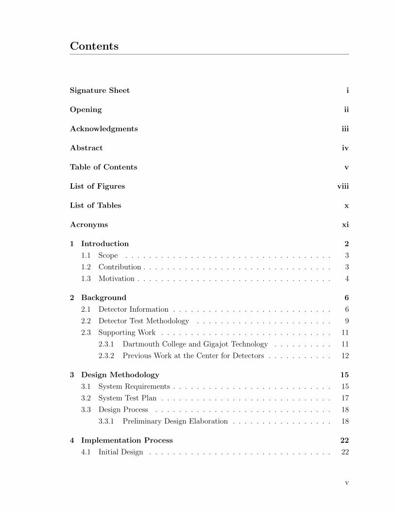
Contents
Signature Sheet i
Opening ii
Acknowledgments iii
Abstract iv
Table of Contents v
List of Figures viii
List of Tables x
Acronyms xi
1 Introduction 2
1.1 Scope . . . . . . . . . . . . . . . . . . . . . . . . . . . . . . . . . . . 3
1.2 Contribution . . . . . . . . . . . . . . . . . . . . . . . . . . . . . . . . 3
1.3 Motivation . . . . . . . . . . . . . . . . . . . . . . . . . . . . . . . . . 4
2 Background 6
2.1 Detector Information . . . . . . . . . . . . . . . . . . . . . . . . . . . 6
2.2 Detector Test Methodology . . . . . . . . . . . . . . . . . . . . . . . 9
2.3 Supporting Work . . . . . . . . . . . . . . . . . . . . . . . . . . . . . 11
2.3.1 Dartmouth College and Gigajot Technology . . . . . . . . . . 11
2.3.2 Previous Work at the Center for Detectors . . . . . . . . . . . 12
3 Design Methodology 15
3.1 System Requirements . . . . . . . . . . . . . . . . . . . . . . . . . . . 15
3.2 System Test Plan . . . . . . . . . . . . . . . . . . . . . . . . . . . . . 17
3.3 Design Process . . . . . . . . . . . . . . . . . . . . . . . . . . . . . . 18
3.3.1 Preliminary Design Elaboration . . . . . . . . . . . . . . . . . 18
4 Implementation Process 22
4.1 Initial Design . . . . . . . . . . . . . . . . . . . . . . . . . . . . . . . 22
v
CONTENTS
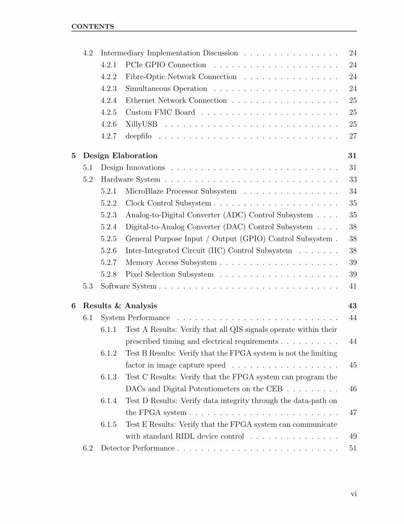
4.2 Intermediary Implementation Discussion . . . . . . . . . . . . . . . . 24
4.2.1 PCIe GPIO Connection . . . . . . . . . . . . . . . . . . . . . 24
4.2.2 Fibre-Optic Network Connection . . . . . . . . . . . . . . . . 24
4.2.3 Simultaneous Operation . . . . . . . . . . . . . . . . . . . . . 24
4.2.4 Ethernet Network Connection . . . . . . . . . . . . . . . . . . 25
4.2.5 Custom FMC Board . . . . . . . . . . . . . . . . . . . . . . . 25
4.2.6 XillyUSB . . . . . . . . . . . . . . . . . . . . . . . . . . . . . 25
4.2.7 deepfifo . . . . . . . . . . . . . . . . . . . . . . . . . . . . . . 27
5 Design Elaboration 31
5.1 Design Innovations . . . . . . . . . . . . . . . . . . . . . . . . . . . . 31
5.2 Hardware System . . . . . . . . . . . . . . . . . . . . . . . . . . . . . 33
5.2.1 MicroBlaze Processor Subsystem . . . . . . . . . . . . . . . . 34
5.2.2 Clock Control Subsystem . . . . . . . . . . . . . . . . . . . . . 35
5.2.3 Analog-to-Digital Converter (ADC) Control Subsystem . . . . 35
5.2.4 Digital-to-Analog Converter (DAC) Control Subsystem . . . . 38
5.2.5 General Purpose Input / Output (GPIO) Control Subsystem . 38
5.2.6 Inter-Integrated Circuit (IIC) Control Subsystem . . . . . . . 38
5.2.7 Memory Access Subsystem . . . . . . . . . . . . . . . . . . . . 39
5.2.8 Pixel Selection Subsystem . . . . . . . . . . . . . . . . . . . . 39
5.3 Software System . . . . . . . . . . . . . . . . . . . . . . . . . . . . . . 41
6 Results & Analysis 43
6.1 System Performance . . . . . . . . . . . . . . . . . . . . . . . . . . . 44
6.1.1 Test A Results: Verify that all QIS signals operate within their
prescribed timing and electrical requirements . . . . . . . . . . 44
6.1.2 Test B Results: Verify that the FPGA system is not the limiting
factor in image capture speed . . . . . . . . . . . . . . . . . . 45
6.1.3 Test C Results: Verify that the FPGA system can program the
DACs and Digital Potentiometers on the CEB . . . . . . . . . 46
6.1.4 Test D Results: Verify data integrity through the data-path on
the FPGA system . . . . . . . . . . . . . . . . . . . . . . . . . 47
6.1.5 Test E Results: Verify that the FPGA system can communicate
with standard RIDL device control . . . . . . . . . . . . . . . 49
6.2 Detector Performance . . . . . . . . . . . . . . . . . . . . . . . . . . . 51
vi
CONTENTS
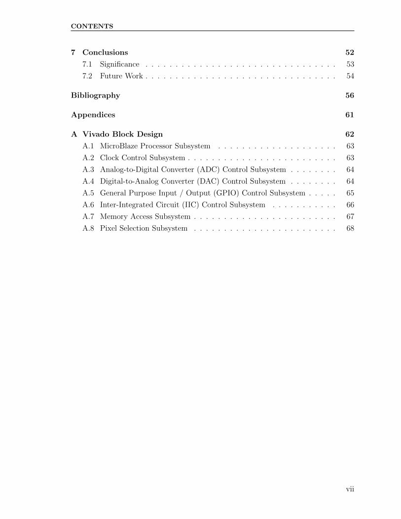
7 Conclusions 52
7.1 Significance . . . . . . . . . . . . . . . . . . . . . . . . . . . . . . . . 53
7.2 Future Work . . . . . . . . . . . . . . . . . . . . . . . . . . . . . . . . 54
Bibliography 56
Appendices 61
A Vivado Block Design 62
A.1 MicroBlaze Processor Subsystem . . . . . . . . . . . . . . . . . . . . 63
A.2 Clock Control Subsystem . . . . . . . . . . . . . . . . . . . . . . . . . 63
A.3 Analog-to-Digital Converter (ADC) Control Subsystem . . . . . . . . 64
A.4 Digital-to-Analog Converter (DAC) Control Subsystem . . . . . . . . 64
A.5 General Purpose Input / Output (GPIO) Control Subsystem . . . . . 65
A.6 Inter-Integrated Circuit (IIC) Control Subsystem . . . . . . . . . . . 66
A.7 Memory Access Subsystem . . . . . . . . . . . . . . . . . . . . . . . . 67
A.8 Pixel Selection Subsystem . . . . . . . . . . . . . . . . . . . . . . . . 68
vii
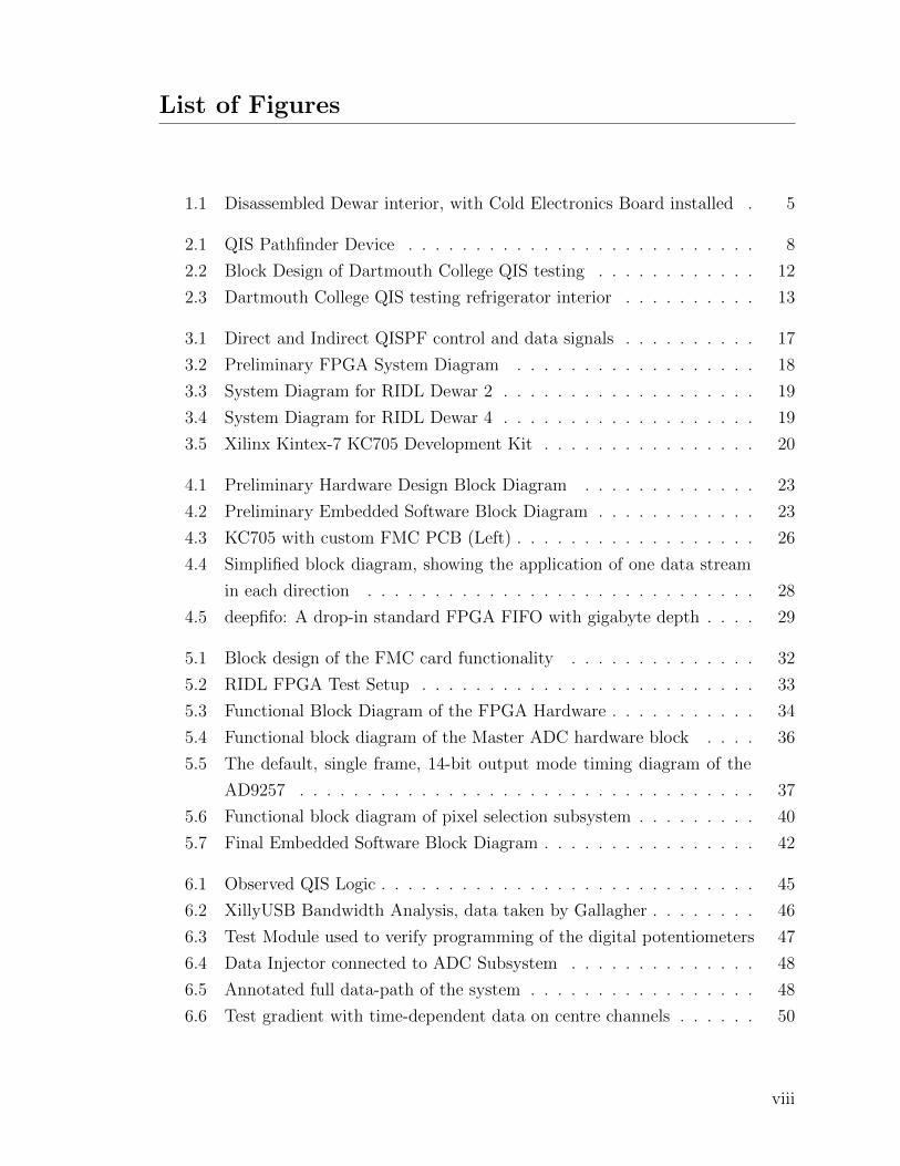
List of Figures
1.1 Disassembled Dewar interior, with Cold Electronics Board installed . 5
2.1 QIS Pathfinder Device . . . . . . . . . . . . . . . . . . . . . . . . . . 8
2.2 Block Design of Dartmouth College QIS testing . . . . . . . . . . . . 12
2.3 Dartmouth College QIS testing refrigerator interior . . . . . . . . . . 13
3.1 Direct and Indirect QISPF control and data signals . . . . . . . . . . 17
3.2 Preliminary FPGA System Diagram . . . . . . . . . . . . . . . . . . 18
3.3 System Diagram for RIDL Dewar 2 . . . . . . . . . . . . . . . . . . . 19
3.4 System Diagram for RIDL Dewar 4 . . . . . . . . . . . . . . . . . . . 19
3.5 Xilinx Kintex-7 KC705 Development Kit . . . . . . . . . . . . . . . . 20
4.1 Preliminary Hardware Design Block Diagram . . . . . . . . . . . . . 23
4.2 Preliminary Embedded Software Block Diagram . . . . . . . . . . . . 23
4.3 KC705 with custom FMC PCB (Left) . . . . . . . . . . . . . . . . . . 26
4.4 Simplified block diagram, showing the application of one data stream
in each direction . . . . . . . . . . . . . . . . . . . . . . . . . . . . . 28
4.5 deepfifo: A drop-in standard FPGA FIFO with gigabyte depth . . . . 29
5.1 Block design of the FMC card functionality . . . . . . . . . . . . . . 32
5.2 RIDL FPGA Test Setup . . . . . . . . . . . . . . . . . . . . . . . . . 33
5.3 Functional Block Diagram of the FPGA Hardware . . . . . . . . . . . 34
5.4 Functional block diagram of the Master ADC hardware block . . . . 36
5.5 The default, single frame, 14-bit output mode timing diagram of the
AD9257 . . . . . . . . . . . . . . . . . . . . . . . . . . . . . . . . . . 37
5.6 Functional block diagram of pixel selection subsystem . . . . . . . . . 40
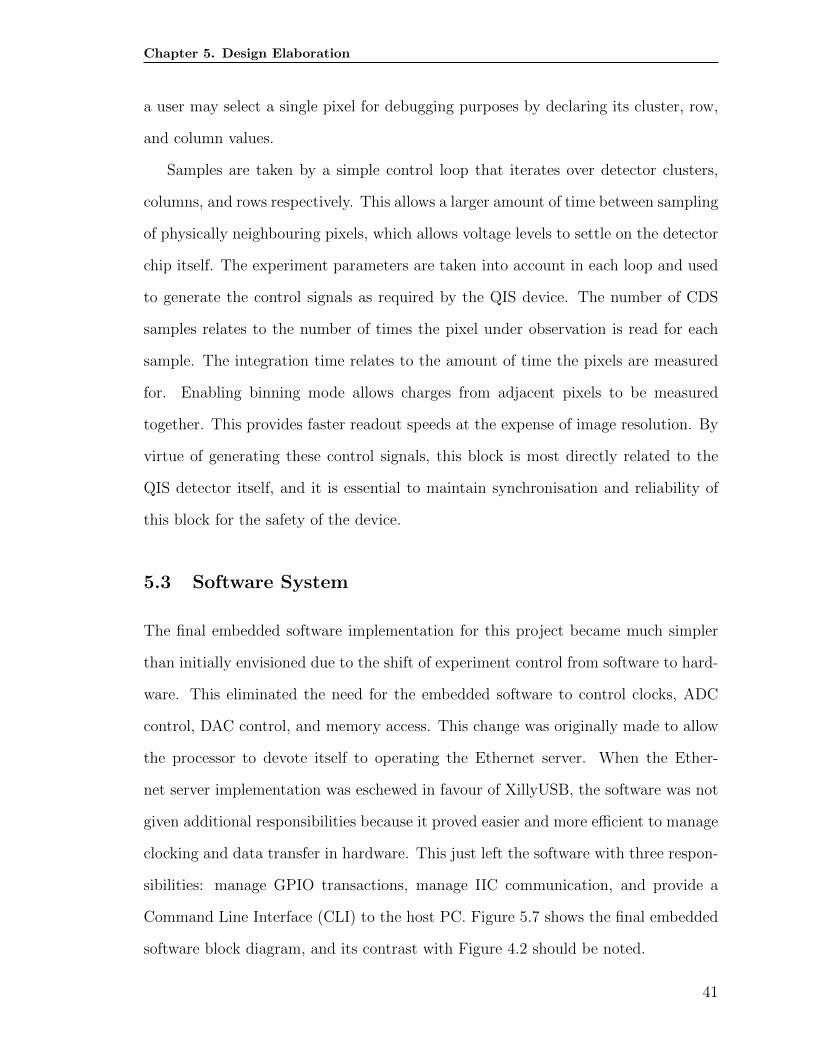
5.7 Final Embedded Software Block Diagram . . . . . . . . . . . . . . . . 42
6.1 Observed QIS Logic . . . . . . . . . . . . . . . . . . . . . . . . . . . . 45
6.2 XillyUSB Bandwidth Analysis, data taken by Gallagher . . . . . . . . 46
6.3 Test Module used to verify programming of the digital potentiometers 47
6.4 Data Injector connected to ADC Subsystem . . . . . . . . . . . . . . 48
6.5 Annotated full data-path of the system . . . . . . . . . . . . . . . . . 48
6.6 Test gradient with time-dependent data on centre channels . . . . . . 50
viii
LIST OF FIGURES
7.1 The QIS Pathfinder device installed into the RIT CfD test setup . . . 53
A.1 Final Vivado Block Design . . . . . . . . . . . . . . . . . . . . . . . . 62
A.2 MicroBlaze processor and peripherals . . . . . . . . . . . . . . . . . . 63
A.3 The “clock block”, responsible for generating clock and synchronisation
signals . . . . . . . . . . . . . . . . . . . . . . . . . . . . . . . . . . . 63
A.4 The ADC block with dual clock functionality . . . . . . . . . . . . . . 64
A.5 The DAC block with included internal GPIO . . . . . . . . . . . . . . 64
A.6 The GPIO interface connected to the FMC ports . . . . . . . . . . . 65
A.7 The IIC block used for digital potentiometers on the CEB . . . . . . 66
A.8 The memory access subsystem, including deepfifo, two internal FIFOs,
and the MIG . . . . . . . . . . . . . . . . . . . . . . . . . . . . . . . 67
A.9 The pixel selection subsystem . . . . . . . . . . . . . . . . . . . . . . 68
ix
List of Tables
2.1 Sensor Specifications . . . . . . . . . . . . . . . . . . . . . . . . . . . 9
3.1 Testing Plan vs. Requirements . . . . . . . . . . . . . . . . . . . . . . 17
3.2 FPGA-generated clocks and patterns for QIS exposures . . . . . . . . 21
5.1 Clock signals and frequencies . . . . . . . . . . . . . . . . . . . . . . 35
6.1 Status of Tests Performed . . . . . . . . . . . . . . . . . . . . . . . . 44
x
Acronyms
ADC
Analog-to-Digital Converter
ATLAST
Advanced Technology Large Aperture Space Telescope
CCD
Charge Coupled Device
CDS
Correlated Double Sampling
CEB
Cold Electronics Board
CfD
Center for Detectors
CIS
CMOS Image Sensor
CMOS
Complementary Metal-Oxide-Semiconductor
COR
Cosmic Origins
DAC
Digital-to-Analog Converter
xi
Acronyms
DDR
Double Data Rate
FIFO
First In First Out
FMC
FPGA Mezzanine Card
FPGA
Field Programmable Gate Array
HabEx
Habitable Exoplanet Observatory
HDI
High Definition Imager
IIC
Inter-Integrated Circuit
JFET
Junction Field Effect Transistor
LUVOIR
Large Ultra Violet / Optical / Infra Red
LVDS
Low-Voltage Differential Signalling
xii
Acronyms
MB
Megabyte
MBps
Megabytes Per Second
MOSFET
Metal Oxide Semiconductor Field Effect Transistor
NASA
National Aeronautics and Space Administration (USA)
PCIe
Peripheral Component Interconnect Express
QIS
Quanta Image Sensor
QISPF
Quanta Image Sensor Path Finder
RAM
Random Access Memory
RIDL
Rochester Imaging Detector Laboratory
RIT
Rochester Institute of Technology
xiii
Acronyms
SAT
Strategic Astrophysics Technology
SFP
Small Form-factor Pluggable
SPI
Serial Peripheral Interface
TRL
Technology Readiness Level
WEB
Warm Electronics Box
1
Chapter 1
Introduction
“Eventually, we reach the dim boundary—the utmost limits of our telescopes. There,
we measure shadows, and we search among ghostly errors of measurement for land-
marks that are scarcely more substantial.” - Dr. Edwin P. Hubble [1]
The NASA Astrophysics Visionary Roadmap describes next-generation missions
that require new technology to be successful [2]. It describes plans for a telescope
known as the Large Ultra-Violet / Optical / Infra-Red (LUVOIR) Surveyor which
requires improved image detection [3]. The Quanta Image Sensor, being a gigapixel-
scalable [4] CMOS photon-number resolving image sensor, would be a strong candi-
date for this application. Additionally, the next-decade flagship mission Habitable
Exoplanet Observatory (HabEx), intended to perform spectroscopy of exoplanet at-
mospheres, would also require a detector with photon-number resolution, radiation
resistance, low power draw, and high dynamic range [5]. The Decadal Survey on As-
tronomy and Astrophysics 2020 mentions these projects as well, and emphasises the
importance of projects such as this one towards strategic flagship missions [6]. Next-
generation detectors such as the QIS are a good match for this application because
of their significant improvements over current optical-wavelength detectors.
2
Chapter 1. Introduction
1.1 Scope
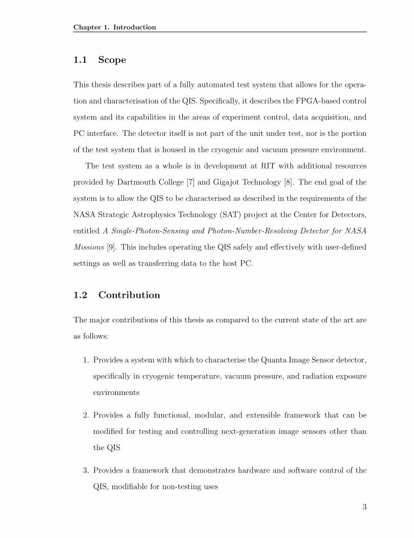
This thesis describes part of a fully automated test system that allows for the opera-
tion and characterisation of the QIS. Specifically, it describes the FPGA-based control
system and its capabilities in the areas of experiment control, data acquisition, and
PC interface. The detector itself is not part of the unit under test, nor is the portion
of the test system that is housed in the cryogenic and vacuum pressure environment.
The test system as a whole is in development at RIT with additional resources
provided by Dartmouth College [7] and Gigajot Technology [8]. The end goal of the
system is to allow the QIS to be characterised as described in the requirements of the
NASA Strategic Astrophysics Technology (SAT) project at the Center for Detectors,
entitled A Single-Photon-Sensing and Photon-Number-Resolving Detector for NASA
Missions [9]. This includes operating the QIS safely and effectively with user-defined
settings as well as transferring data to the host PC.
1.2 Contribution
The major contributions of this thesis as compared to the current state of the art are
as follows:
1. Provides a system with which to characterise the Quanta Image Sensor detector,
specifically in cryogenic temperature, vacuum pressure, and radiation exposure
environments
2. Provides a fully functional, modular, and extensible framework that can be
modified for testing and controlling next-generation image sensors other than
the QIS
3. Provides a framework that demonstrates hardware and software control of the
QIS, modifiable for non-testing uses
3
Chapter 1. Introduction
1.3 Motivation
Currently, there is no existing system for the cryogenic and vacuum-pressure testing of
a Quanta Image Sensor. There exist systems for standard temperature and pressure
testing at Dartmouth College and Gigajot Technology [8]. Additionally, there exists
at the RIT Center for Detectors a robust cryogenic and vacuum-pressure testing
system for detectors other than the QIS. The testing procedure at RIT involves the
following subsystems.
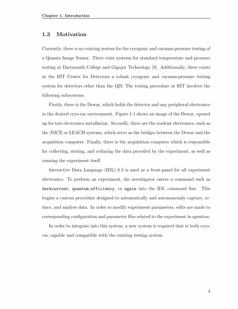
Firstly, there is the Dewar, which holds the detector and any peripheral electronics
in the desired cryo-vac environment. Figure 1.1 shows an image of the Dewar, opened
up for test electronics installation. Secondly, there are the readout electronics, such as
the JMCE or LEACH systems, which serve as the bridges between the Dewar and the
acquisition computer. Finally, there is the acquisition computer which is responsible
for collecting, storing, and reducing the data provided by the experiment, as well as
running the experiment itself.
Interactive Data Language (IDL) 6.3 is used as a front-panel for all experiment
electronics. To perform an experiment, the investigator enters a command such as
darkcurrent, quantum efficiency, or egain into the IDL command line. This
begins a custom procedure designed to automatically and autonomously capture, re-
duce, and analyse data. In order to modify experiment parameters, edits are made to
corresponding configuration and parameter files related to the experiment in question.
In order to integrate into this system, a new system is required that is both cryo-
vac capable and compatible with the existing testing system.
4
Chapter 1. Introduction
Figure 1.1: Disassembled Dewar interior, with Cold Electronics Board installed
5
Chapter 2
Background
2.1 Detector Information
An image sensor is a device that turns electromagnetic radiation into electronic signals
[10]. The two main types of digital image sensor used today are the Charge-Coupled
Device (CCD) and the CMOS active-pixel sensor (APS). For now, CMOS image
sensors (CIS) are used in lower cost and lower power draw environments. CCDs are
generally used when image fidelity is the highest priority, such as in broadcast video
cameras or, in this case, astrophotography [11]. However, this may change due to
next-generation CMOS sensors achieving comparable or favourable results to CCDs.
One such next-generation sensor is the Quanta Image Sensor, or QIS. The QIS,
developed by Dr. Eric Fossum and his team at Dartmouth College, is a concept for
a CMOS image sensor that operates similarly to a photographic plate and that can
be scaled to gigapixel resolutions [4]. Similarly to a photographic plate, each photon
that enters the detector will change the state of a resolution element. For each pixel
on the QIS, a zero reports no photons detected and a one reports one or more photons
detected. As Equation (2.1) shows, the charge generated by the arrival of a photon
is directly related to the voltage output. The primary innovation of the QIS is the
pixel design, as it allows for a capacitance as low as 0.4 fF [12]. The voltage response
to a single photo-generated electron event with a small capacitance is large and is
6
Chapter 2. Background
known as conversion gain, measured in µV per electron. As seen in Equation (2.2)
the calculated conversion gain at a capacitance of 0.4 fF is 400µV per electron. Dr.
Fossum and his team report a gain of up to 420µV per electron [13].
V =q
C(2.1)
0.0004V =1.602 176 62× 10−19C
4× 10⁻¹⁶ F(2.2)
The readout architecture maintains low noise during operation through the use of
design and correlated double sampling. The combination of low-capacitance and low
noise allows the QIS to achieve single photon sensing and photon number resolution
at room temperature [14]. Because of the limited full-well depth of the detector,
the values from the QIS must be read out in real time to prevent loss of data [15].
Future QIS versions include modifications such as on-chip multi-bit ADCs as well as
significantly larger full-well depth [16] [17].
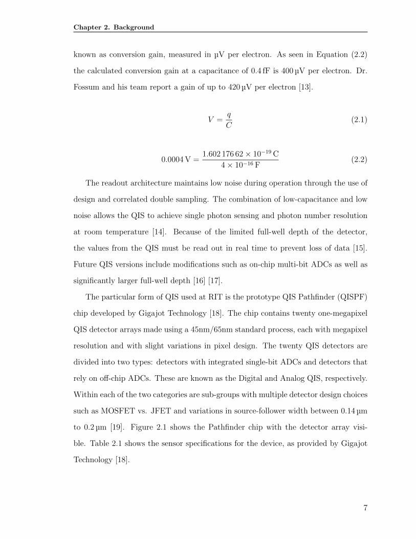
The particular form of QIS used at RIT is the prototype QIS Pathfinder (QISPF)
chip developed by Gigajot Technology [18]. The chip contains twenty one-megapixel
QIS detector arrays made using a 45nm/65nm standard process, each with megapixel
resolution and with slight variations in pixel design. The twenty QIS detectors are
divided into two types: detectors with integrated single-bit ADCs and detectors that
rely on off-chip ADCs. These are known as the Digital and Analog QIS, respectively.
Within each of the two categories are sub-groups with multiple detector design choices
such as MOSFET vs. JFET and variations in source-follower width between 0.14 µm
to 0.2 µm [19]. Figure 2.1 shows the Pathfinder chip with the detector array visi-
ble. Table 2.1 shows the sensor specifications for the device, as provided by Gigajot
Technology [18].
7
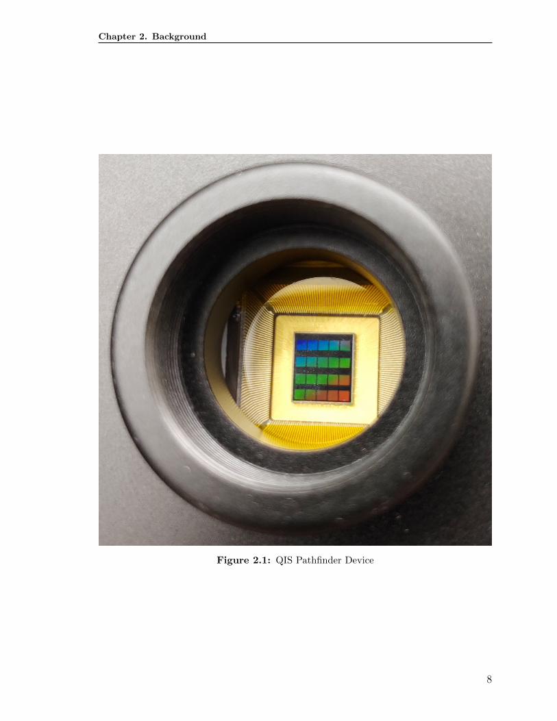
Chapter 2. Background
Figure 2.1: QIS Pathfinder Device
8
Chapter 2. Background
Table 2.1: Sensor Specifications
Type of Sensor 1st Generation Quanta Image SensorResolution 1020 X 1020 Active PixelsPixel Size 1.1 µm X 1.1 µmSensor Format 1.1mm X 1.1mmShutter Mode Cluster-Parallel Rolling ShutterRead Noise (Typ.) As Low As 0.24e- RMS @ 20CDark Current (Typ.) 0.068e-/Sec/Pixel @ 20CQuantum Efficiency (Typ.) Up To 87%Full-Well Capacity 200e-
2.2 Detector Test Methodology
Detectors can be characterised to illustrate their performance at research organisa-
tions such as the Center for Detectors. The performance of detectors varies strongly
with respect to temperature. The method of cooling detectors reduces dark current
and read noise. It has long been used to improve efficiency of detectors, although
room-temperature functionality is generally preferred [20].
Detectors are characterised based on commonly used performance metrics, which
correlate with the list of experiments run at the Center for Detectors. These metrics
are as follows:
1. Output Efficiency: Measures the device’s overall ratio of incoming to detected
photons.
2. Conversion Gain: Measures the average ratio of electrons per single Analog-to-
Digital Unit.
3. Read Noise: Measures the variance in detector output based on environmental
noise at the input, averaged over all pixels of the device.
4. Dark Current: Measures the detector output current over long exposures with
9
Chapter 2. Background
no external radiation at different temperatures. It is caused by the electrons
naturally freed from the valence band and collected within the potential well of
a pixel.
5. Quantum Efficiency (QE): Measures the detector’s light sensitivity by count-
ing the number of charge carriers and comparing with the number of photons
the detector is exposed to. This is measured with varying wavelengths to mea-
sure efficiency at varied photon energy levels and represents the percentage of
incoming photons that the device can successfully detect.
6. Linearity: Measures the relationship between photons detected and Analog-to-
Digital Units. A linear relationship is ideal.
7. Full Well Depth: Measures the maximum number of electrons that can be stored
in a pixel’s potential well before the electrons can no longer be confined.
8. Persistence: Measures the lifetime and quantity of electrons that remain in
the substrate after a bright source causes overexposure. This can be seen as
after-images or, in extreme cases, dead pixels or pixel areas.
9. Cross-talk: Measures the amount of charge diffused between an active and
inactive pixel.
10. Inter-pixel Capacitance (IPC): Measures the voltage change on neighbouring
pixels based on the amount of charge built up on a target pixel.
These tests are run by taking large amounts of controlled data through the detector
readout system, reducing the data to its important parts, and then analysing results.
At the Center for Detectors, the data reduction and analysis are done outside of the
detector readout chain on dedicated machines so as to provide a centralised data
manipulation centre [21]. This means that various readout electronics may provide
data in different ways, but the data is manipulated in the same way in all cases. This
10
Chapter 2. Background
also means that the readout electronics themselves do not modify or analyse the data
themselves, but rather provide all of the data, in the proper format, to the reduction
and analysis machines. This list of tests comprises the end goal of this system as
a whole. The FPGA system described in this thesis presents the link between the
data computers and the hardware related to the detector itself, and is crucial to the
completion of the system as a whole.
2.3 Supporting Work
2.3.1 Dartmouth College and Gigajot Technology
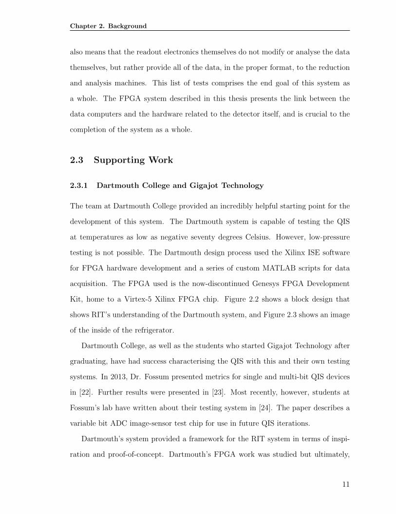
The team at Dartmouth College provided an incredibly helpful starting point for the
development of this system. The Dartmouth system is capable of testing the QIS
at temperatures as low as negative seventy degrees Celsius. However, low-pressure
testing is not possible. The Dartmouth design process used the Xilinx ISE software
for FPGA hardware development and a series of custom MATLAB scripts for data
acquisition. The FPGA used is the now-discontinued Genesys FPGA Development
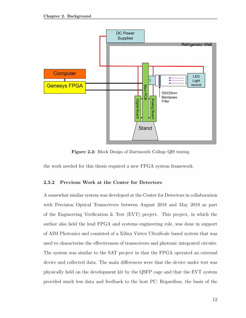
Kit, home to a Virtex-5 Xilinx FPGA chip. Figure 2.2 shows a block design that
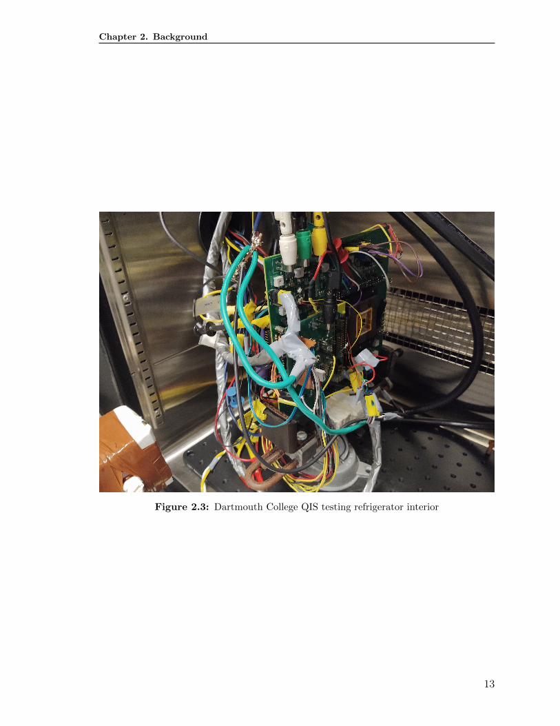
shows RIT’s understanding of the Dartmouth system, and Figure 2.3 shows an image
of the inside of the refrigerator.
Dartmouth College, as well as the students who started Gigajot Technology after
graduating, have had success characterising the QIS with this and their own testing
systems. In 2013, Dr. Fossum presented metrics for single and multi-bit QIS devices
in [22]. Further results were presented in [23]. Most recently, however, students at
Fossum’s lab have written about their testing system in [24]. The paper describes a
variable bit ADC image-sensor test chip for use in future QIS iterations.
Dartmouth’s system provided a framework for the RIT system in terms of inspi-
ration and proof-of-concept. Dartmouth’s FPGA work was studied but ultimately,
11
Chapter 2. Background
Figure 2.2: Block Design of Dartmouth College QIS testing
the work needed for this thesis required a new FPGA system framework.
2.3.2 Previous Work at the Center for Detectors
A somewhat similar system was developed at the Center for Detectors in collaboration
with Precision Optical Transceivers between August 2018 and May 2019 as part
of the Engineering Verification & Test (EVT) project. This project, in which the
author also held the lead FPGA and systems engineering role, was done in support
of AIM Photonics and consisted of a Xilinx Virtex UltraScale based system that was
used to characterise the effectiveness of transceivers and photonic integrated circuits.
The system was similar to the SAT project in that the FPGA operated an external
device and collected data. The main differences were that the device under test was
physically held on the development kit by the QSFP cage and that the EVT system
provided much less data and feedback to the host PC. Regardless, the basis of the
12
Chapter 2. Background
Figure 2.3: Dartmouth College QIS testing refrigerator interior
13

Chapter 2. Background
EVT project was used as a rough guideline for the framework of the SAT project.
Despite the hardware, software, and environmental differences, the conceptual design
blocks were maintained between the two projects.
14
Chapter 3
Design Methodology
3.1 System Requirements
Much of the time and effort invested into this thesis involved the research and planning
required to create a functional system. Of course, as with any project, requirements
and considerations were updated throughout the design and implementation cycle,
but the first major task in creating the system was to determine the exact system
requirements.
The initial system requirements review for the FPGA subsystem was held in July
2020. The reason why an FPGA was chosen for this project was because of their
suitability to high-speed data transmission as well as their previous use at the CfD.
The The main goals of the system were to use the PC as a front panel to operate the
cold electronics board (CEB) and the QIS, transfer commands and data between the
PC and the CEB, and provide clocking and synchronisation signals for the CEB and
the QIS [25]. The formal list of system requirements is as follows:
1. The FPGA system will be able to clock the QIS in accordance with Dartmouth
College’s specifications.
2. The FPGA system will be able to perform at the rate of one full image per
second.
15
Chapter 3. Design Methodology
3. The FPGA system will be able to process input from the PC and use it to
control experiment variations and to program components on the CEB.
4. The FPGA system will be able to capture the sixteen stream outputs from the
CEB and present them to the PC in a reasonable data format.
5. The FPGA system will deliver all raw data (i.e. without reduction) to the PC
for reduction and analysis.
6. The FPGA system will utilise an off-the-shelf FPGA development kit.
7. The FPGA system will allow bidirectional communication between the PC and
the CEB.
8. The FPGA system will use an IDL / C / C++ DLL to enable IDL support.
9. The FPGA system will be powered by its included DC power supply.
These requirements were chosen as a team during the preliminary planning phase
of this work. They were agreed upon based on the necessary functionality as well as
on the availability of developmental and financial resources.
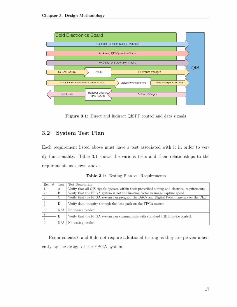
Several of these requirements involve controlling the CEB and the QIS. The signals
needed to satisfy that requirement are signals that either directly or indirectly control
the QIS. Figure 3.1 shows a diagram of the signals sent to and received from the
QISPF through the CEB.
The direct control signals are passed through the CEB and sent to the QIS as-is,
while the indirect control signals are used to control peripherals on the CEB which
then output their own signals to the QIS. The three arrows that illustrate the direct
control signals correspond to the clock signals shown in Table 3.2.
16
Chapter 3. Design Methodology
Figure 3.1: Direct and Indirect QISPF control and data signals
3.2 System Test Plan
Each requirement listed above must have a test associated with it in order to ver-
ify functionality. Table 3.1 shows the various tests and their relationships to the
requirements as shown above.
Table 3.1: Testing Plan vs. Requirements
Req. # Test Test Description1 A Verify that all QIS signals operate within their prescribed timing and electrical requirements.2 B Verify that the FPGA system is not the limiting factor in image capture speed.3 C Verify that the FPGA system can program the DACs and Digital Potentiometers on the CEB.4
D Verify data integrity through the data-path on the FPGA system.56 N/A No testing needed.7
E Verify that the FPGA system can communicate with standard RIDL device control.89 N/A No testing needed.
Requirements 6 and 9 do not require additional testing as they are proven inher-
ently by the design of the FPGA system.
17
Chapter 3. Design Methodology
3.3 Design Process
The nature of FPGA design work in general as well as the specific nature of this
project provides a strong basis for an iterative design process. The process consisted
of a proposed design being presented and checked against the pre-determined set of
system requirements. If a proposed design met the requirements, the most complex
or unknown facets of it were quickly prototyped as a basic proof of concept. Once the
prototype system was complete, it was then evaluated for functionality and perfor-
mance. Any shortcomings were then noted to be improved in subsequent iterations.
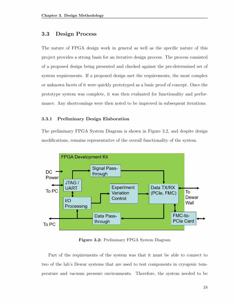
3.3.1 Preliminary Design Elaboration
The preliminary FPGA System Diagram is shown in Figure 3.2, and despite design
modifications, remains representative of the overall functionality of the system.
Figure 3.2: Preliminary FPGA System Diagram
Part of the requirements of the system was that it must be able to connect to
two of the lab’s Dewar systems that are used to test components in cryogenic tem-
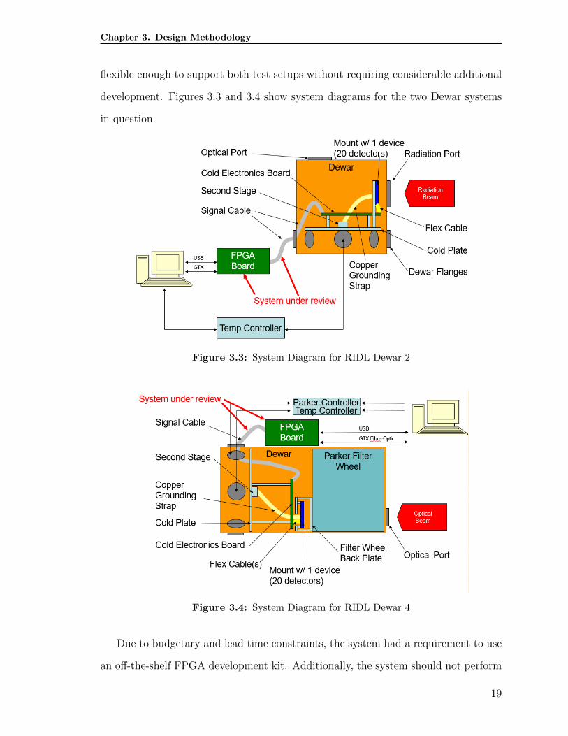
perature and vacuum pressure environments. Therefore, the system needed to be
18
Chapter 3. Design Methodology
flexible enough to support both test setups without requiring considerable additional
development. Figures 3.3 and 3.4 show system diagrams for the two Dewar systems
in question.
Figure 3.3: System Diagram for RIDL Dewar 2
Figure 3.4: System Diagram for RIDL Dewar 4
Due to budgetary and lead time constraints, the system had a requirement to use
an off-the-shelf FPGA development kit. Additionally, the system should not perform
19
Chapter 3. Design Methodology
any data reduction or analysis on its own and should provide every piece of data to
the host PC.
The primary function of the system, however, is to operate the QIS itself with
settings provided by a user at the host PC. The user must be able to make variations
to each experiment chosen. These variations included integration time, sequential vs
simultaneous pixel mode, the number of Correlated Double Samples (CDS), and the
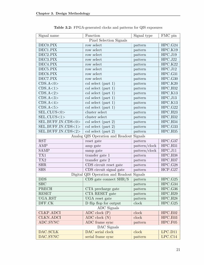
state of certain QIS binary control signals. Table 3.2 shows all signals that the FPGA
is responsible for controlling [26].
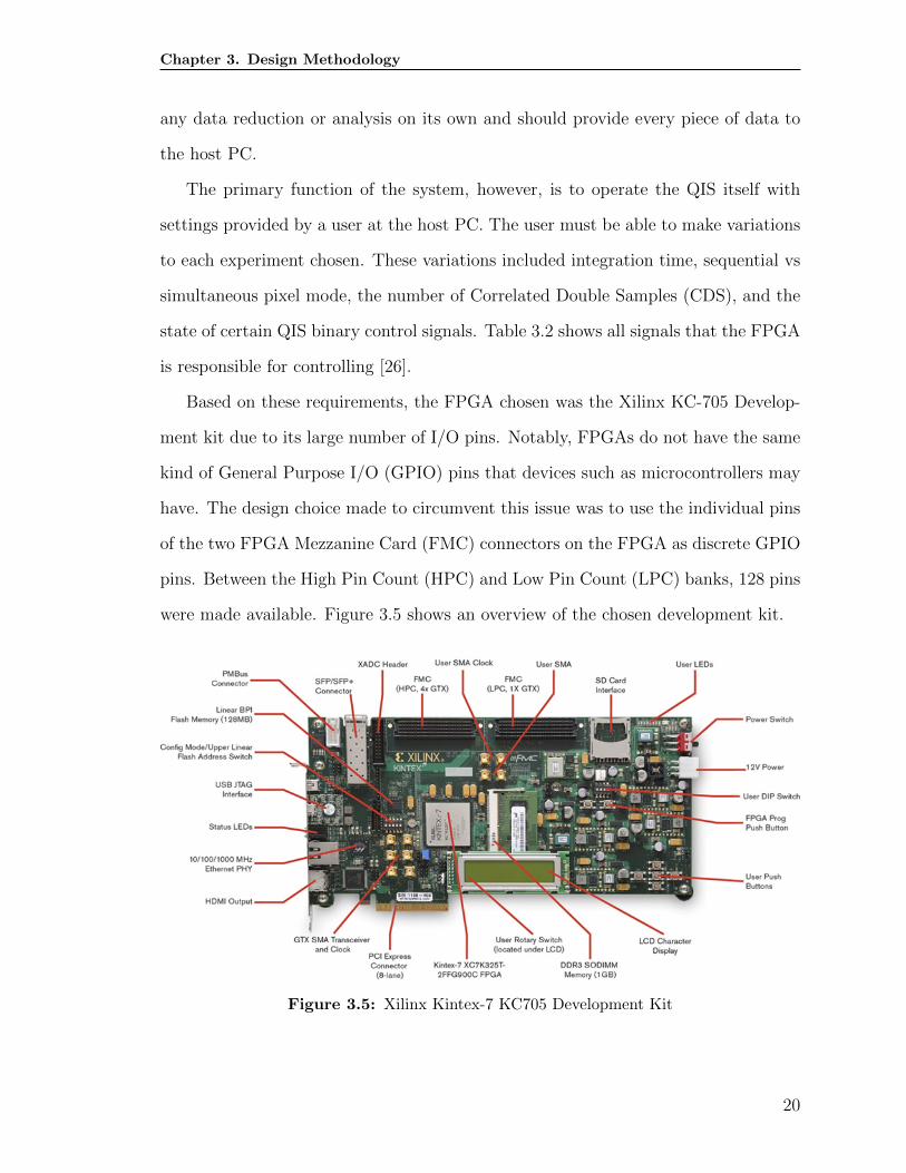
Based on these requirements, the FPGA chosen was the Xilinx KC-705 Develop-
ment kit due to its large number of I/O pins. Notably, FPGAs do not have the same
kind of General Purpose I/O (GPIO) pins that devices such as microcontrollers may
have. The design choice made to circumvent this issue was to use the individual pins
of the two FPGA Mezzanine Card (FMC) connectors on the FPGA as discrete GPIO
pins. Between the High Pin Count (HPC) and Low Pin Count (LPC) banks, 128 pins
were made available. Figure 3.5 shows an overview of the chosen development kit.
Figure 3.5: Xilinx Kintex-7 KC705 Development Kit
20
Chapter 3. Design Methodology
Table 3.2: FPGA-generated clocks and patterns for QIS exposures
Signal name Function Signal type FMC pinPixel Selection Signals
DEC0 PIX row select pattern HPC G24DEC1 PIX row select pattern HPC K19DEC2 PIX row select pattern HPC J19DEC3 PIX row select pattern HPC J22DEC4 PIX row select pattern HPC K22DEC5 PIX row select pattern HPC J12DEC6 PIX row select pattern HPC G31DEC7 PIX row select pattern HPC G30CDS A<0> col select (part 1) pattern HPC K20CDS A<1> col select (part 1) pattern HPC H32CDS A<2> col select (part 1) pattern HPC K13CDS A<3> col select (part 1) pattern HPC J13CDS A<4> col select (part 1) pattern HPC K13CDS A<5> col select (part 1) pattern HPC G22SEL CLUS<0> cluster select pattern HPC H23SEL CLUS<1> cluster select pattern HPC H32SEL BUFF IN CDS<0> col select (part 2) pattern HPC H34SEL BUFF IN CDS<1> col select (part 2) pattern HPC G33SEL BUFF IN CDS<2> col select (part 2) pattern HPC H35
Analog QIS Operation and Readout SignalsRST reset gate pattern HPC G37AMP amp gate pattern/clock HPC H31SAMP samp gate pattern/clock HPC J11TX1 transfer gate 1 pattern HPC H38TX2 transfer gate 2 pattern HPC H37SHR CDS circuit reset gate pattern HPC G28SHS CDS circuit signal gate pattern HCP G27
Digital QIS Operation and Readout SignalsDDS CDS gate connect SHR/S pattern HPC G25SHC pattern HPC G34PRECH CTA precharge gate pattern HPC G36RESET CTA RESET gate pattern HPC H29UGA RST UGA reset gate pattern HPC H28DFF CK D flip flop for output clock HPC G25
ADC SignalsCLKP ADCI ADC clock (P) clock HPC E02CLKN ADCI ADC clock (N) clock HPC E03ADC SYNC ADC frame sync pattern HPC F05
DAC SignalsDAC SCLK DAC serial clock clock LPC D11DAC SYNC serial frame sync pattern LPC C14
21
Chapter 4
Implementation Process
An iterative design process was used to complete the design and implementation of
this FPGA hardware and software suite. As such, parts of the initial design were
implemented until errors or roadblocks were found. Each difficulty was then investi-
gated and researched until either a solution or an alternative design choice was found.
These intermediary implementation cycles are discussed here for future reference and
for reader edification.
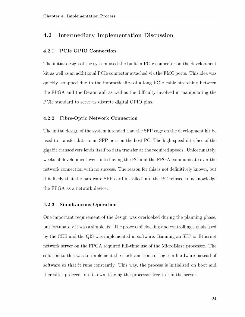
4.1 Initial Design
The very first proposed design consisted of three main connections. The first was
the UART over serial connection between the development kit and the host PC used
to provide a terminal interface for either a user or the automated testing system.
The second was the FPGA-to-PC data pipeline, implemented via GTX transceivers
over fibre-optic cables. Finally, there was the connection between the Dewar and the
FPGA which used two PCIe cables, one of which would be attached to the FMC-to-
PCIe adapter connected to the KC705.
The computational power of the FPGA development kit would be provided by a
MicroBlaze processor, a Xilinx soft microprocessor core. The core would be provided
with an embedded software program. Figure 4.1 shows the initial block design of the
FPGA hardware and Figure 4.2 shows the design of the embedded software.
22
Chapter 4. Implementation Process
Figure 4.1: Preliminary Hardware Design Block Diagram
Figure 4.2: Preliminary Embedded Software Block Diagram
23
Chapter 4. Implementation Process
4.2 Intermediary Implementation Discussion
4.2.1 PCIe GPIO Connection
The initial design of the system used the built-in PCIe connector on the development
kit as well as an additional PCIe connector attached via the FMC ports. This idea was
quickly scrapped due to the impracticality of a long PCIe cable stretching between
the FPGA and the Dewar wall as well as the difficulty involved in manipulating the
PCIe standard to serve as discrete digital GPIO pins.
4.2.2 Fibre-Optic Network Connection
The initial design of the system intended that the SFP cage on the development kit be
used to transfer data to an SFP port on the host PC. The high-speed interface of the
gigabit transceivers lends itself to data transfer at the required speeds. Unfortunately,
weeks of development went into having the PC and the FPGA communicate over the
network connection with no success. The reason for this is not definitively known, but
it is likely that the hardware SFP card installed into the PC refused to acknowledge
the FPGA as a network device.
4.2.3 Simultaneous Operation
One important requirement of the design was overlooked during the planning phase,
but fortunately it was a simple fix. The process of clocking and controlling signals used
by the CEB and the QIS was implemented in software. Running an SFP or Ethernet
network server on the FPGA required full-time use of the MicroBlaze processor. The
solution to this was to implement the clock and control logic in hardware instead of
software so that it runs constantly. This way, the process is initialised on boot and
thereafter proceeds on its own, leaving the processor free to run the server.
24
Chapter 4. Implementation Process
4.2.4 Ethernet Network Connection
One of the steps taken in the debugging process was to haphazardly replace the SFP
cable with a standard Ethernet cable and modify the design accordingly. After doing
this, the PC was able to recognise and communicate with the FPGA via basic tests
such as an echo server. This method of data transfer was pursued nearly to the point
of success. The FPGA was able to send data packets to the PC and have them
retain integrity. While investigating memory access and custom buffering solutions
for the Ethernet subsystem, however, the team discovered deepfifo [27] and thereby
XillyUSB [28]. The development path was moved to the XillyUSB ecosystem due to
the fact that the Ethernet subsystem required a license of $650 and the license to use
the XillyUSB ecosystem was provided free of charge for academic use.
4.2.5 Custom FMC Board
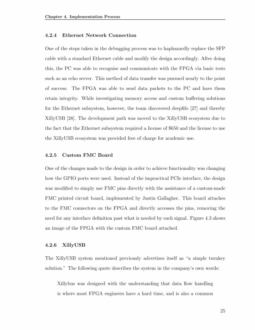
One of the changes made to the design in order to achieve functionality was changing
how the GPIO ports were used. Instead of the impractical PCIe interface, the design
was modified to simply use FMC pins directly with the assistance of a custom-made
FMC printed circuit board, implemented by Justin Gallagher. This board attaches
to the FMC connectors on the FPGA and directly accesses the pins, removing the
need for any interface definition past what is needed by each signal. Figure 4.3 shows
an image of the FPGA with the custom FMC board attached.
4.2.6 XillyUSB
The XillyUSB system mentioned previously advertises itself as “a simple turnkey
solution.” The following quote describes the system in the company’s own words:
Xillybus was designed with the understanding that data flow handling
is where most FPGA engineers have a hard time, and is also a common
25
Chapter 4. Implementation Process
Figure 4.3: KC705 with custom FMC PCB (Left)
26
Chapter 4. Implementation Process
reason for bugs. Fluctuations in application data supply and demand tend
to generate rarely reached states in the logic, often revealing hidden bugs
which are extremely difficult to tackle.
Accordingly, Xillybus doesn’t just supply a wrapper for the underlying
transport (e.g. a PCIe DMA engine), but offers several end-to-end stream
pipes for application data transport. This is a “once-and-for-all” solution,
which has undergone heavy stress testing on numerous FPGA platforms
and IP core configurations. Robustness and dependability can’t be speci-
fied on a datasheet, but are easily told while testing. Luckily, integrating
Xillybus with a target application for real-life stress testing is a relatively
simple task, so evaluating its worthiness is an immediate and low-risk
assignment. [28]
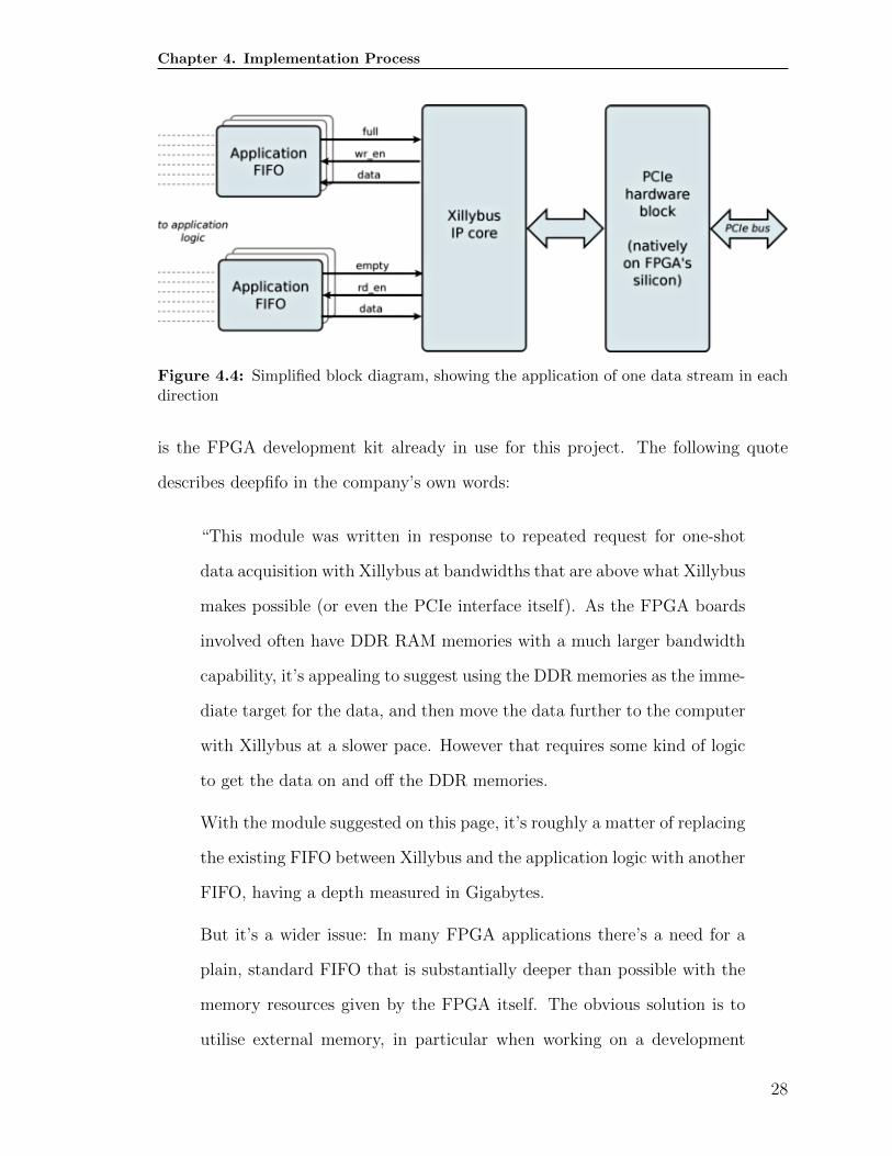
Figure 4.4 shows the company’s provided block diagram for the system. The
system was used in place of Ethernet or fibre-optic communication between the FPGA
and PC due to its meeting the requirements for data rate and stability and being a
pre-tested solution. This solution was not available when the planning for this project
was completed, and this is why it was only discovered as part of the iterative design
process.
In practice, Xillybus proved to be very useful and relatively simple to implement
into this design. It proved to be simpler and more reliable than the TCP/IP imple-
mentation in testing.
4.2.7 deepfifo
The solution to memory access and buffering on the FPGA was also provided by the
Xillybus company. It is called deepfifo and is described as “a drop-in standard FPGA
FIFO with gigabyte depth.” It also happens to be most tested on the KC705, which
27
Chapter 4. Implementation Process
Figure 4.4: Simplified block diagram, showing the application of one data stream in eachdirection
is the FPGA development kit already in use for this project. The following quote
describes deepfifo in the company’s own words:
“This module was written in response to repeated request for one-shot
data acquisition with Xillybus at bandwidths that are above what Xillybus
makes possible (or even the PCIe interface itself). As the FPGA boards
involved often have DDR RAM memories with a much larger bandwidth
capability, it’s appealing to suggest using the DDR memories as the imme-
diate target for the data, and then move the data further to the computer
with Xillybus at a slower pace. However that requires some kind of logic
to get the data on and off the DDR memories.
With the module suggested on this page, it’s roughly a matter of replacing
the existing FIFO between Xillybus and the application logic with another
FIFO, having a depth measured in Gigabytes.
But it’s a wider issue: In many FPGA applications there’s a need for a
plain, standard FIFO that is substantially deeper than possible with the
memory resources given by the FPGA itself. The obvious solution is to
utilise external memory, in particular when working on a development
28
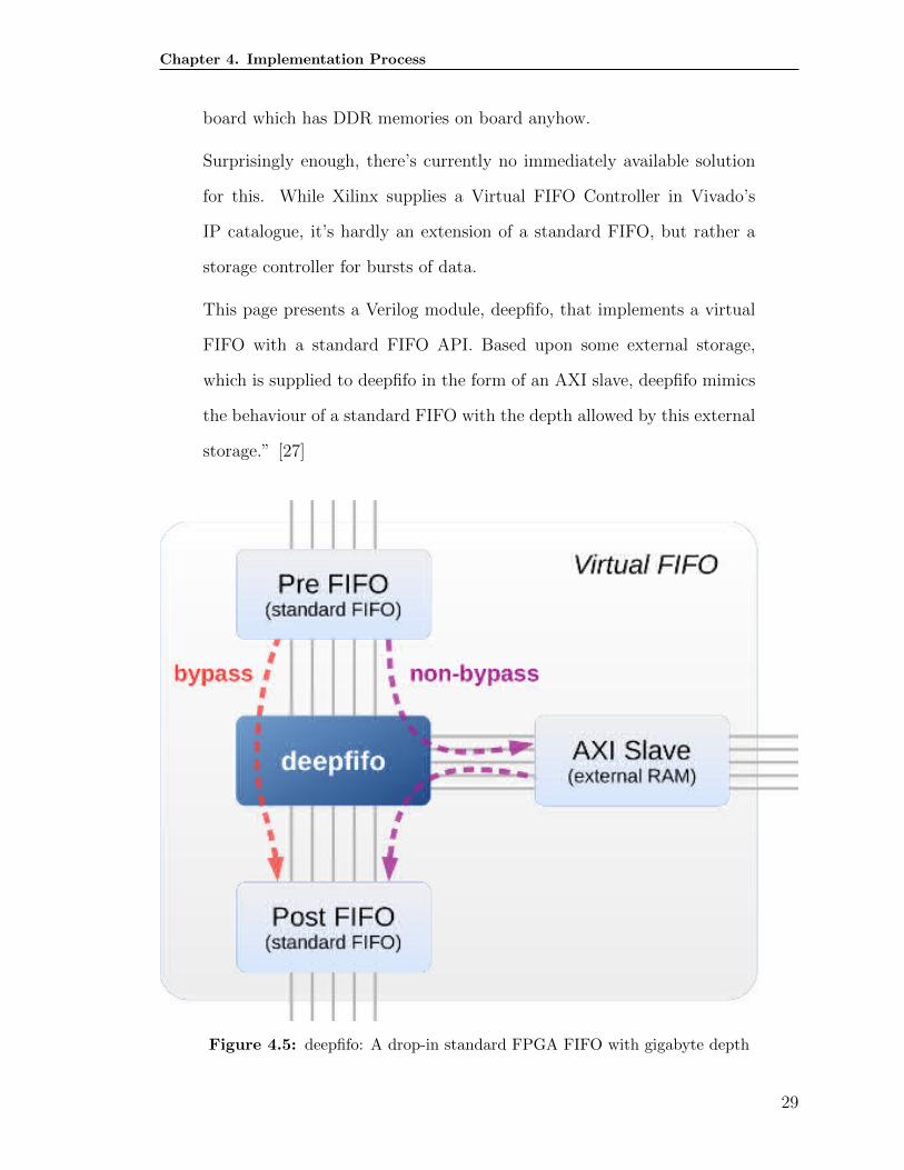
Chapter 4. Implementation Process
board which has DDR memories on board anyhow.
Surprisingly enough, there’s currently no immediately available solution
for this. While Xilinx supplies a Virtual FIFO Controller in Vivado’s
IP catalogue, it’s hardly an extension of a standard FIFO, but rather a
storage controller for bursts of data.
This page presents a Verilog module, deepfifo, that implements a virtual
FIFO with a standard FIFO API. Based upon some external storage,
which is supplied to deepfifo in the form of an AXI slave, deepfifo mimics
the behaviour of a standard FIFO with the depth allowed by this external
storage.” [27]
Figure 4.5: deepfifo: A drop-in standard FPGA FIFO with gigabyte depth
29
Chapter 4. Implementation Process
In this hardware design, this module serves as a stand-in for the direct memory
access system in place to support the Ethernet subsystem. The design was modified
to use this module instead due to it being pre-tested, which allowed the team to
save development time and reassign resources to other tasks. Figure 4.5 shows the
company’s provided block diagram. The described implementation instructions were
followed and proved to be an adequate guide to using the hardware.
30
Chapter 5
Design Elaboration
5.1 Design Innovations
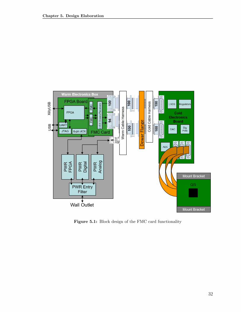
The most important distinction of this system from the others that are in use in-
volves the use of the Dewar. By splitting QIS control and data acquisition between
the FPGA system and the cold electronics board, it presents the ability to test the
detector in a cryo-vac environment. This is a significant innovation to Dartmouth
College’s design, as their readout detector PCB and digital / analog readout elec-
tronics are all attached to each other. This prohibits installation into a Dewar. By
separating the system into a detector head, cold electronics, and warm electronics,
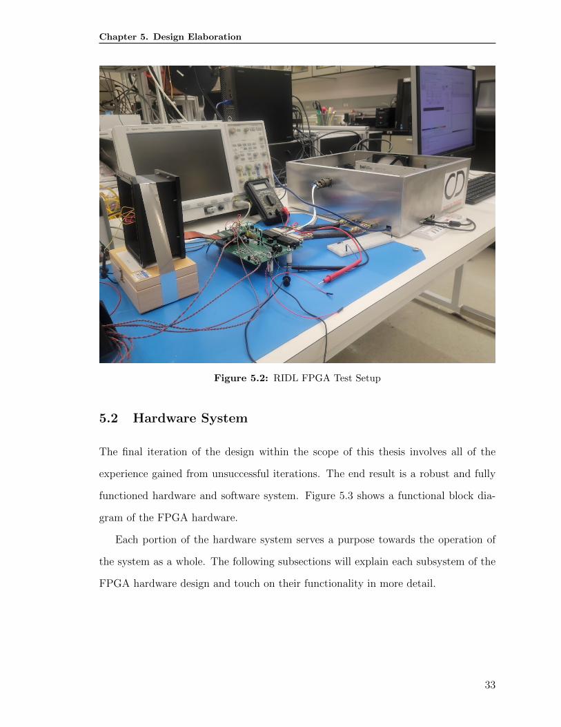
RIT will be able to perform space-environment testing. Figure 5.1 shows a block
diagram of the RIT testing system with included Dewar wall. Figure 5.2 shows the
physical testing setup used at RIT, with the three distinct parts of the system visible.
The detector head and cold electronics subsystems were designed specifically for
use in a Dewar, and as such have very specific limitations on size and shape of
electronics. This affects the rest of the design in terms of part selection, cable length,
and overall design topology. Because of the custom peripherals as well as the need
to transport data through the Dewar wall, Dartmouth’s FPGA system could not be
used for this application. Therefore, a new hardware and software system was needed.
31
Chapter 5. Design Elaboration
Figure 5.1: Block design of the FMC card functionality
32
Chapter 5. Design Elaboration
Figure 5.2: RIDL FPGA Test Setup
5.2 Hardware System
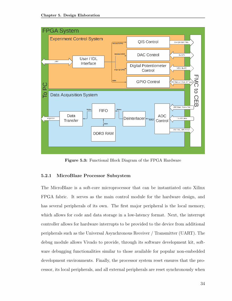
The final iteration of the design within the scope of this thesis involves all of the
experience gained from unsuccessful iterations. The end result is a robust and fully
functioned hardware and software system. Figure 5.3 shows a functional block dia-
gram of the FPGA hardware.
Each portion of the hardware system serves a purpose towards the operation of
the system as a whole. The following subsections will explain each subsystem of the
FPGA hardware design and touch on their functionality in more detail.
33
Chapter 5. Design Elaboration
Figure 5.3: Functional Block Diagram of the FPGA Hardware
5.2.1 MicroBlaze Processor Subsystem
The MicroBlaze is a soft-core microprocessor that can be instantiated onto Xilinx
FPGA fabric. It serves as the main control module for the hardware design, and
has several peripherals of its own. The first major peripheral is the local memory,
which allows for code and data storage in a low-latency format. Next, the interrupt
controller allows for hardware interrupts to be provided to the device from additional
peripherals such as the Universal Asynchronous Receiver / Transmitter (UART). The
debug module allows Vivado to provide, through its software development kit, soft-
ware debugging functionalities similar to those available for popular non-embedded
development environments. Finally, the processor system reset ensures that the pro-
cessor, its local peripherals, and all external peripherals are reset synchronously when
34
Chapter 5. Design Elaboration
a reset command is received or when the physical reset button on the board is pressed.
The software itself that is running on the processor is detailed in Section 5.3.
5.2.2 Clock Control Subsystem
Timing for this system was provided by a series of Xilinx Clocking Wizards. The
Clocking Wizards were noted to provide insufficiently precise period and frequency
values when they were asked for more than three high-speed clock outputs, so the
need for clock outputs was split across three such Clocking Wizards. Table 5.1 shows
all of the system’s clock signals. The ui clk signal is not visible in this subsystem,
but it will be shown in the memory access subsystem.
Table 5.1: Clock signals and frequencies
Clock Name Frequency (MHz) Usageclk 200 main 200 Provides a single-ended clock to subsequent clocking wizardsclk 350 350 Operates Integrated Logic Analysersclk 200 mb 200 Operates the MicroBlaze processor and its local peripheralsclk 140 140 Operates the pixel select and ADC hardware subsystemsclk 8 8 Operates the DAC hardware subsystemclk 280 280 Allows the ADC hardware block to retrieve data at the proper timeui clk 200 Generated by the MIG, operates deepfifo and RAM peripherals
5.2.3 Analog-to-Digital Converter (ADC) Control Subsystem
An important distinction must be made regarding the ADC Control Subsystem: the
subsystem does not perform the Analog-to-digital conversion itself, but rather controls
the 14-bit ADC devices present on the Cold Electronics Board. Due to the high-speed
nature of the data acquisition related to this project, the ADC controller serves a
number of purposes. They are as follows:
1. Create a differential clock for the ADC chips.
2. Create a synchronisation signal for the ADC chips.
3. Read and buffer data output by the ADC chips.
35
Chapter 5. Design Elaboration
4. Provide data to the Memory Access Subsystem.
5. Report to the Memory Access Subsystem when it is safe to read provided data.
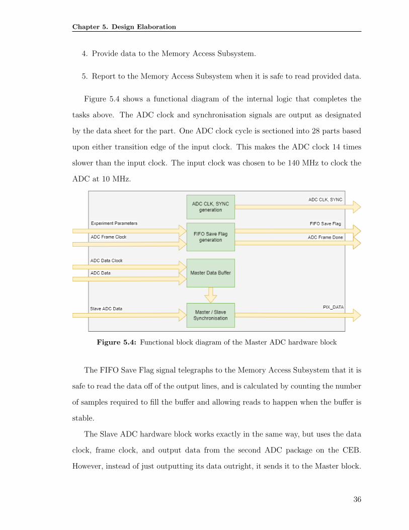
Figure 5.4 shows a functional diagram of the internal logic that completes the
tasks above. The ADC clock and synchronisation signals are output as designated
by the data sheet for the part. One ADC clock cycle is sectioned into 28 parts based
upon either transition edge of the input clock. This makes the ADC clock 14 times
slower than the input clock. The input clock was chosen to be 140 MHz to clock the
ADC at 10 MHz.
Figure 5.4: Functional block diagram of the Master ADC hardware block
The FIFO Save Flag signal telegraphs to the Memory Access Subsystem that it is
safe to read the data off of the output lines, and is calculated by counting the number
of samples required to fill the buffer and allowing reads to happen when the buffer is
stable.
The Slave ADC hardware block works exactly in the same way, but uses the data
clock, frame clock, and output data from the second ADC package on the CEB.
However, instead of just outputting its data outright, it sends it to the Master block.
36
Chapter 5. Design Elaboration
The Master block then synchronises both sets of data lines to the data clock of the
first ADC package to avoid issues when reading.
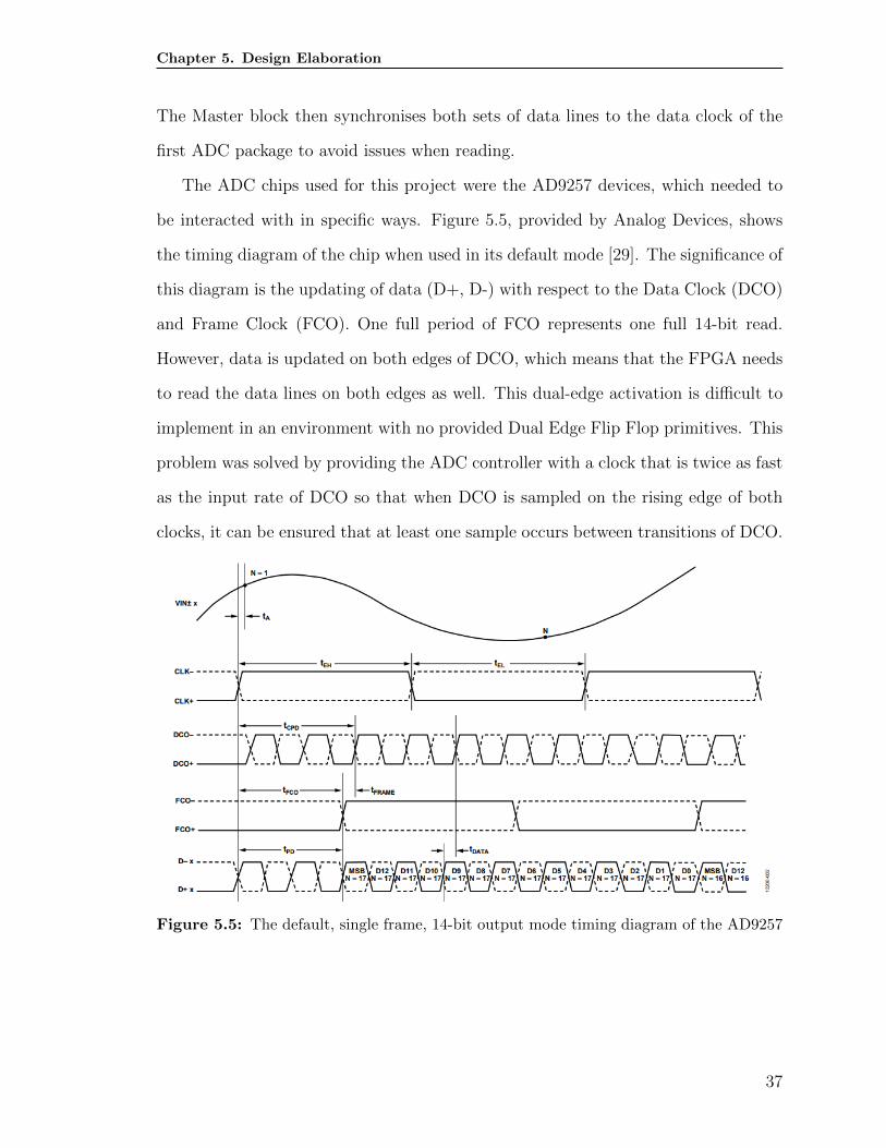
The ADC chips used for this project were the AD9257 devices, which needed to
be interacted with in specific ways. Figure 5.5, provided by Analog Devices, shows
the timing diagram of the chip when used in its default mode [29]. The significance of
this diagram is the updating of data (D+, D-) with respect to the Data Clock (DCO)
and Frame Clock (FCO). One full period of FCO represents one full 14-bit read.
However, data is updated on both edges of DCO, which means that the FPGA needs
to read the data lines on both edges as well. This dual-edge activation is difficult to
implement in an environment with no provided Dual Edge Flip Flop primitives. This
problem was solved by providing the ADC controller with a clock that is twice as fast
as the input rate of DCO so that when DCO is sampled on the rising edge of both
clocks, it can be ensured that at least one sample occurs between transitions of DCO.
Figure 5.5: The default, single frame, 14-bit output mode timing diagram of the AD9257
37
Chapter 5. Design Elaboration
5.2.4 Digital-to-Analog Converter (DAC) Control Subsystem
The DAC Control Subsystem operates similarly to the ADC controller, albeit with
fewer specific considerations. The chip used for this project is the AD5372 32-channel
DAC, and the CEB uses this device to control voltage levels without breaking vac-
uum. On the FPGA, the controller is operated by a simple internal GPIO interface.
Instead of exposing the GPIO pins to off-chip peripherals as is typical, they are sim-
ply connected to the hardware block on the FPGA fabric. This allows for simple and
user-friendly control from the MicroBlaze embedded software. The DAC chips them-
selves are responsible for providing reference voltages to the QIS. The data format
for DAC control is standard Serial Peripheral Interface (SPI) and does not need any
specific programming past what is mentioned in the part’s documentation.
5.2.5 General Purpose Input / Output (GPIO) Control Subsystem
The GPIO subsystem on the FPGA is very simple. It connects external pins on
the FMC connector array to the MicroBlaze so that their state can be modified in
software. This is used for signals such as amplifier bypass, specific peripheral resets,
and 3.3 volt power connections. Because the majority of the GPIO connections
required are taken care of by other subsystems, e.g. the ADC Control Subsystem,
most of the additional connections available through this subsystem are unused, but
are provided for the sake of future updates or extensions.
5.2.6 Inter-Integrated Circuit (IIC) Control Subsystem
The IIC peripherals used on this FPGA are reserved solely for the programming of
four groups of digital potentiometer devices on the cold electronics board. These
digital potentiometers are used to fine-tune bias current and voltage levels so as to
meet the operational requirements of the QIS.
38
Chapter 5. Design Elaboration
5.2.7 Memory Access Subsystem
The final implementation of the Memory Access Subsystem consists of a Xilinx Mem-
ory Interface Generator (MIG) used to communicate directly with the 1-gigabyte
DDR3 Random Access Memory (RAM) module on the FPGA development kit. The
RAM unit is used as a data buffer in case the FPGA is able to generate data more
quickly than the host PC can read it out. This buffering is enabled by the Xillybus
deepfifo module[27]. As requested in the implementation directions for deepfifo, the
FPGA provides it with two small FIFO primitives. Due to the high rate of speed
achieved by the readout software on the host PC, deepfifo is always empty. Future
projects may be simplified by removing it and replacing it with a larger on-chip FPGA
FIFO, but there is no reason seen to remove it from this project at this time. It does
not introduce any notable latency to the data chain and serves as a fall-back to be
used if the PC cannot perform data read commands for any reason. Figure 4.5 serves
as a reference for the intended operation of deepfifo.
The FPGA FIFOs, as well as deepfifo, are run off of the ui clk generated by the
MIG. This is to ensure that all time-sensitive events occurring within the Memory
Access Subsystem are synchronised to the hardware of the RAM controller itself.
This minimises the possibility of data collisions that can be caused by the use of two
separate clocks in one data pipeline.
5.2.8 Pixel Selection Subsystem
The final hardware subsystem used is the Pixel Selection Subsystem. This system,
like the DAC Control Subsystem, is operated by an internal GPIO interface. This
interface provides crucial information from the MicroBlaze subsystem, such as the
number of Correlated Double Sampling (CDS) samples or the desired integration
time for the exposure. The Pixel Select Subsystem is responsible for a large number
of necessary control signals, as follows:
39
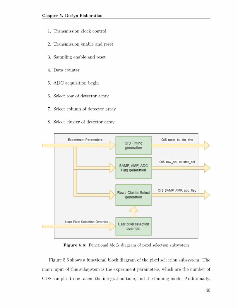
Chapter 5. Design Elaboration
1. Transmission clock control
2. Transmission enable and reset
3. Sampling enable and reset
4. Data counter
5. ADC acquisition begin
6. Select row of detector array
7. Select column of detector array
8. Select cluster of detector array
Figure 5.6: Functional block diagram of pixel selection subsystem
Figure 5.6 shows a functional block diagram of the pixel selection subsystem. The
main input of this subsystem is the experiment parameters, which are the number of
CDS samples to be taken, the integration time, and the binning mode. Additionally,
40
Chapter 5. Design Elaboration
a user may select a single pixel for debugging purposes by declaring its cluster, row,
and column values.
Samples are taken by a simple control loop that iterates over detector clusters,
columns, and rows respectively. This allows a larger amount of time between sampling
of physically neighbouring pixels, which allows voltage levels to settle on the detector
chip itself. The experiment parameters are taken into account in each loop and used
to generate the control signals as required by the QIS device. The number of CDS
samples relates to the number of times the pixel under observation is read for each
sample. The integration time relates to the amount of time the pixels are measured
for. Enabling binning mode allows charges from adjacent pixels to be measured
together. This provides faster readout speeds at the expense of image resolution. By
virtue of generating these control signals, this block is most directly related to the
QIS detector itself, and it is essential to maintain synchronisation and reliability of
this block for the safety of the device.
5.3 Software System
The final embedded software implementation for this project became much simpler
than initially envisioned due to the shift of experiment control from software to hard-
ware. This eliminated the need for the embedded software to control clocks, ADC
control, DAC control, and memory access. This change was originally made to allow
the processor to devote itself to operating the Ethernet server. When the Ether-
net server implementation was eschewed in favour of XillyUSB, the software was not
given additional responsibilities because it proved easier and more efficient to manage
clocking and data transfer in hardware. This just left the software with three respon-
sibilities: manage GPIO transactions, manage IIC communication, and provide a
Command Line Interface (CLI) to the host PC. Figure 5.7 shows the final embedded
software block diagram, and its contrast with Figure 4.2 should be noted.
41
Chapter 5. Design Elaboration
Figure 5.7: Final Embedded Software Block Diagram
42
Chapter 6
Results & Analysis
Although the project as a whole is still underway, a great amount of progress was made
over the course of the work for this thesis. The requirements mentioned in Section
3.1 have all been met. Those requirements are reproduced here for convenience:
1. The FPGA system will be able to clock the QIS in accordance with Dartmouth
College’s specifications.
2. The FPGA system will be able to perform at the rate of one full image per
second.
3. The FPGA system will be able to process input from the PC and use it to
control experiment variations and to program components on the CEB.
4. The FPGA system will be able to capture the sixteen stream outputs from the
CEB and present them to the PC in a reasonable data format.
5. The FPGA system will deliver all raw data (i.e. without reduction) to the PC
for reduction and analysis.
6. The FPGA system will utilise an off-the-shelf FPGA development kit.
7. The FPGA system will allow bidirectional communication between the PC and
the CEB.
43
Chapter 6. Results & Analysis
8. The FPGA system will use an IDL / C / C++ Digitally Linked Library (DLL)
to enable IDL support.
9. The FPGA system will be powered by its included DC power supply.
6.1 System Performance
Table 6.1 is a copy of Table 3.1 but with the addition of the results of each test
performed.
Table 6.1: Status of Tests Performed
Req. # Test Test Description Test Status1 A Verify that all QIS signals operate within their prescribed timing and electrical requirements. PASS2 B Verify that the FPGA system is not the limiting factor in image capture speed. PASS3 C Verify that the FPGA system can program the DACs and Digital Potentiometers on the CEB. PASS4
D Verify data integrity through the data-path on the FPGA system. PASS56 N/A No testing needed. N/A7
E Verify that the FPGA system can communicate with standard RIDL device control. PASS89 N/A No testing needed. N/A
6.1.1 Test A Results: Verify that all QIS signals operate within their
prescribed timing and electrical requirements
Because of the cost and scarcity of the QIS device itself, it is incredibly important to
ensure that all signals and clocks are operating within acceptable parameters before
the device is installed. To this end, an external digital logic analyser was used to
record all data that would have gone to the QIS device and confirm its compatibility
with the requirements given by Dartmouth College [7]. The purpose of this test is to
ensure there are no unexpected or unintended signal changes or pulses occurring that
may damage the QIS.
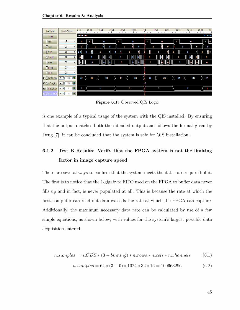
Figure 6.1 shows the output of a digital logic analyser that samples at the QIS chip
carrier as one part of a series of tests. It was generated with the system in standard
experiment operation mode, with a CDS value of 4 and binning mode disabled. This
44
Chapter 6. Results & Analysis
Figure 6.1: Observed QIS Logic
is one example of a typical usage of the system with the QIS installed. By ensuring
that the output matches both the intended output and follows the format given by
Deng [7], it can be concluded that the system is safe for QIS installation.
6.1.2 Test B Results: Verify that the FPGA system is not the limiting
factor in image capture speed
There are several ways to confirm that the system meets the data-rate required of it.
The first is to notice that the 1-gigabyte FIFO used on the FPGA to buffer data never
fills up and in fact, is never populated at all. This is because the rate at which the
host computer can read out data exceeds the rate at which the FPGA can capture.
Additionally, the maximum necessary data rate can be calculated by use of a few
simple equations, as shown below, with values for the system’s largest possible data
acquisition entered.
n samples = n CDS ∗ (3− binning) ∗ n rows ∗ n cols ∗ n channels (6.1)
n samples = 64 ∗ (3− 0) ∗ 1024 ∗ 32 ∗ 16 = 100663296 (6.2)
45
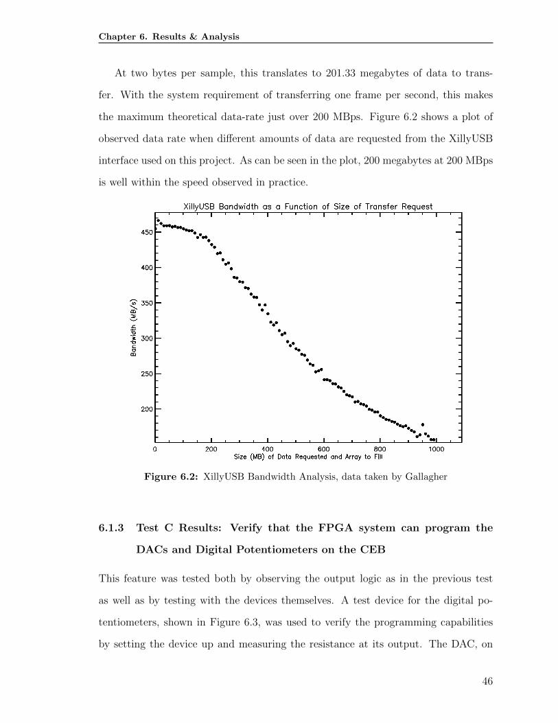
Chapter 6. Results & Analysis
At two bytes per sample, this translates to 201.33 megabytes of data to trans-
fer. With the system requirement of transferring one frame per second, this makes
the maximum theoretical data-rate just over 200 MBps. Figure 6.2 shows a plot of
observed data rate when different amounts of data are requested from the XillyUSB
interface used on this project. As can be seen in the plot, 200 megabytes at 200 MBps
is well within the speed observed in practice.
Figure 6.2: XillyUSB Bandwidth Analysis, data taken by Gallagher
6.1.3 Test C Results: Verify that the FPGA system can program the
DACs and Digital Potentiometers on the CEB
This feature was tested both by observing the output logic as in the previous test
as well as by testing with the devices themselves. A test device for the digital po-
tentiometers, shown in Figure 6.3, was used to verify the programming capabilities
by setting the device up and measuring the resistance at its output. The DAC, on
46
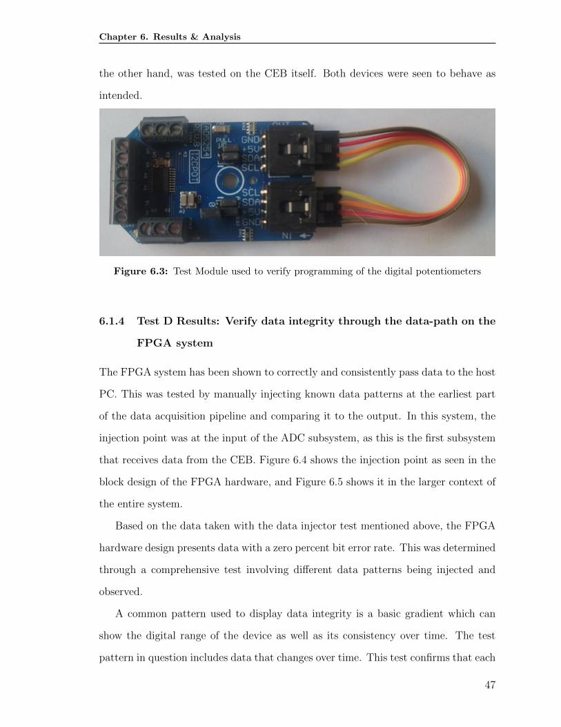
Chapter 6. Results & Analysis
the other hand, was tested on the CEB itself. Both devices were seen to behave as
intended.
Figure 6.3: Test Module used to verify programming of the digital potentiometers
6.1.4 Test D Results: Verify data integrity through the data-path on the
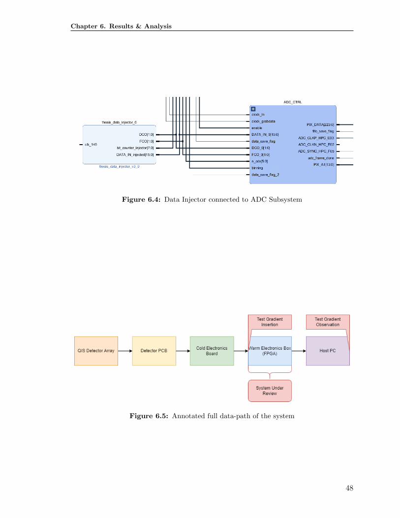
FPGA system
The FPGA system has been shown to correctly and consistently pass data to the host
PC. This was tested by manually injecting known data patterns at the earliest part
of the data acquisition pipeline and comparing it to the output. In this system, the
injection point was at the input of the ADC subsystem, as this is the first subsystem
that receives data from the CEB. Figure 6.4 shows the injection point as seen in the
block design of the FPGA hardware, and Figure 6.5 shows it in the larger context of
the entire system.
Based on the data taken with the data injector test mentioned above, the FPGA
hardware design presents data with a zero percent bit error rate. This was determined
through a comprehensive test involving different data patterns being injected and
observed.
A common pattern used to display data integrity is a basic gradient which can
show the digital range of the device as well as its consistency over time. The test
pattern in question includes data that changes over time. This test confirms that each
47
Chapter 6. Results & Analysis
Figure 6.4: Data Injector connected to ADC Subsystem
Figure 6.5: Annotated full data-path of the system
48
Chapter 6. Results & Analysis
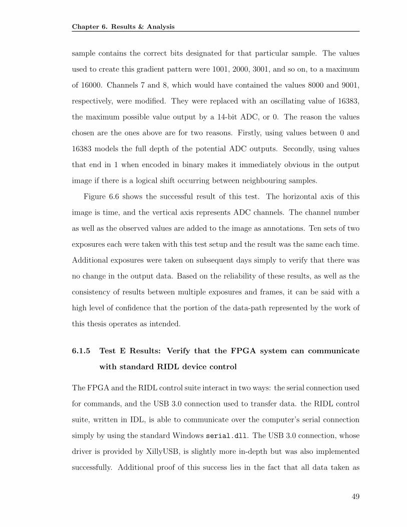
sample contains the correct bits designated for that particular sample. The values
used to create this gradient pattern were 1001, 2000, 3001, and so on, to a maximum
of 16000. Channels 7 and 8, which would have contained the values 8000 and 9001,
respectively, were modified. They were replaced with an oscillating value of 16383,
the maximum possible value output by a 14-bit ADC, or 0. The reason the values
chosen are the ones above are for two reasons. Firstly, using values between 0 and
16383 models the full depth of the potential ADC outputs. Secondly, using values
that end in 1 when encoded in binary makes it immediately obvious in the output
image if there is a logical shift occurring between neighbouring samples.
Figure 6.6 shows the successful result of this test. The horizontal axis of this
image is time, and the vertical axis represents ADC channels. The channel number
as well as the observed values are added to the image as annotations. Ten sets of two
exposures each were taken with this test setup and the result was the same each time.
Additional exposures were taken on subsequent days simply to verify that there was
no change in the output data. Based on the reliability of these results, as well as the
consistency of results between multiple exposures and frames, it can be said with a
high level of confidence that the portion of the data-path represented by the work of
this thesis operates as intended.
6.1.5 Test E Results: Verify that the FPGA system can communicate
with standard RIDL device control
The FPGA and the RIDL control suite interact in two ways: the serial connection used
for commands, and the USB 3.0 connection used to transfer data. the RIDL control
suite, written in IDL, is able to communicate over the computer’s serial connection
simply by using the standard Windows serial.dll. The USB 3.0 connection, whose
driver is provided by XillyUSB, is slightly more in-depth but was also implemented
successfully. Additional proof of this success lies in the fact that all data taken as
49
Chapter 6. Results & Analysis
Figure 6.6: Test gradient with time-dependent data on centre channels
50
Chapter 6. Results & Analysis
part of Section 6.1.4 was taken through the XillyUSB connection.
6.2 Detector Performance
Unfortunately, the detector itself has not yet been characterised due to the remainder
of the data path remaining in development. Even though the scope of this thesis does
not include the full testing system, the work done here does represent a baseline from
which the detector can be properly characterised and tested without concern about
data integrity on the FPGA itself. It also provides a safe control system for the QIS
that has been tested to minimise the possibility of damage tot he device. The next
steps in order to complete the detector characterisation include optimising the system
for the specific detector chip by slightly modifying bias currents and voltages as well
as verifying the functionality of the detector head and cold electronics board.
51
Chapter 7
Conclusions
Advancements in detector technology require custom readout, control, and testing
systems in order to create practical applications. This thesis details one such system.
The result of this thesis was not only a successful FPGA-based data pipeline system
for the QIS, but also a framework for future implementations. All things considered,
the FPGA system functioned as expected and intended, despite issues encountered
in the design and implementation process. Although the project as a whole remains
in development, the system described in this thesis provides a functional and safe
foundation that can be used through the end of this project and a baseline for future
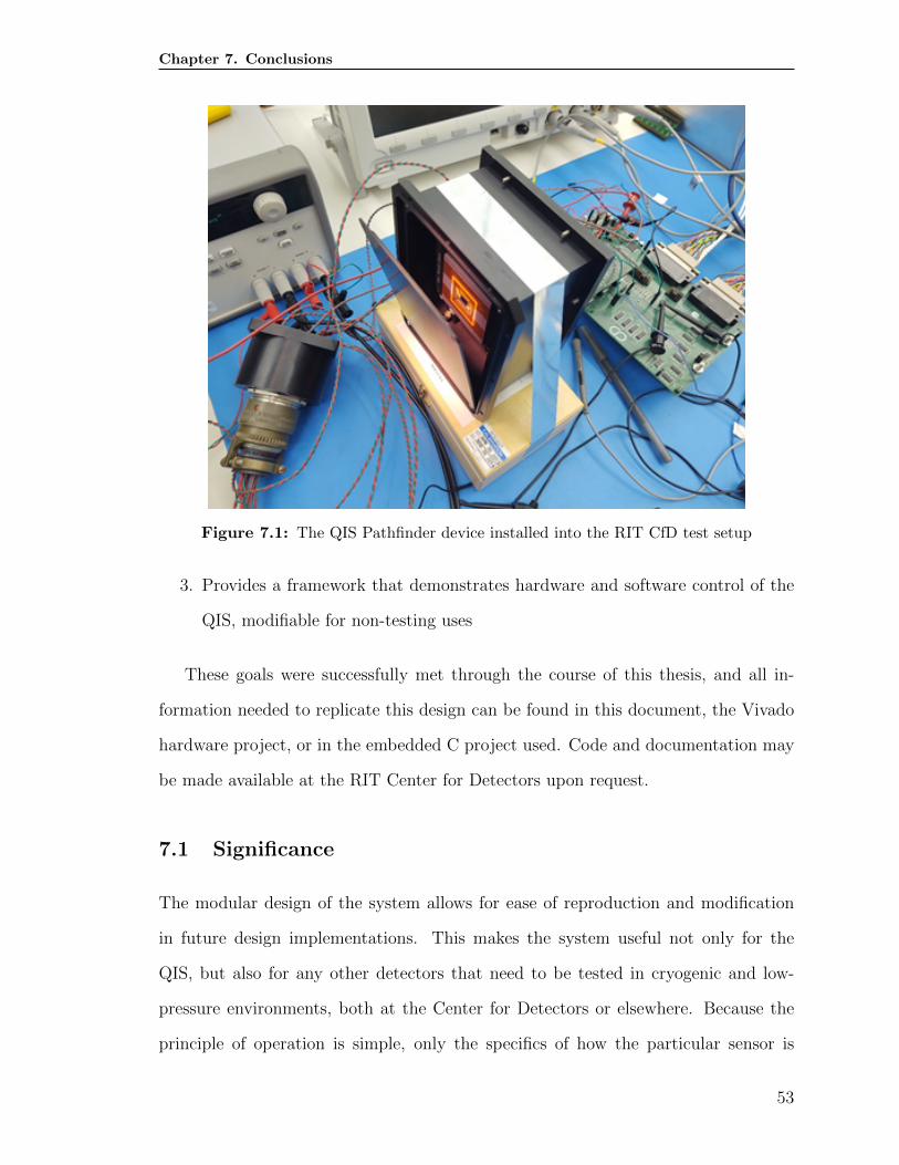
projects. Figure 7.1 shows an image of the QIS device installed into the test electronics
at the RIT Center for Detectors.
As mentioned in Section 1.2, the major contributions of this thesis as compared
to the current state of the art are as follows:
1. Provides a system with which to characterise the Quanta Image Sensor detector,
specifically in cryogenic temperature, vacuum pressure, and radiation exposure
environments
2. Provides a fully functional, modular, and extensible framework that can be
modified for testing and controlling next-generation image sensors other than
the QIS
52
Chapter 7. Conclusions
Figure 7.1: The QIS Pathfinder device installed into the RIT CfD test setup
3. Provides a framework that demonstrates hardware and software control of the
QIS, modifiable for non-testing uses
These goals were successfully met through the course of this thesis, and all in-
formation needed to replicate this design can be found in this document, the Vivado
hardware project, or in the embedded C project used. Code and documentation may
be made available at the RIT Center for Detectors upon request.
7.1 Significance
The modular design of the system allows for ease of reproduction and modification
in future design implementations. This makes the system useful not only for the
QIS, but also for any other detectors that need to be tested in cryogenic and low-
pressure environments, both at the Center for Detectors or elsewhere. Because the
principle of operation is simple, only the specifics of how the particular sensor is
53
Chapter 7. Conclusions
operated must be changed. Additionally, this provides a baseline design for alternative
uses that may also require high-speed or real-time data acquisition. Furthermore, it
provides a functional interface that can be modified to fit any application that requires
communication to an FPGA from an IDL or serial port connection. Despite the fact
that IDL is not as commonly used as it once was, the same FPGA software can be
used to interact with a C programming-based driver, as it simply relies on native
Windows serial port functionality.
7.2 Future Work
The system as it stands can be used to evaluate the QIS detector array towards the
end of advancing its Technology Readiness Level, but it also holds the potential for
upgrades and extensions in the future. As Gigajot Technology continues to iterate on
the QIS device, this system can be modified slightly in order to test each iteration of
the device and provide feedback on how it may be improved. Additionally, the system
can be expanded to provide additional functionality that is not currently implemented,
such as the ability to use the QIS device as a real-time camera for testing purposes.
Furthermore, the cryo-vac capabilities of this test system allows for the possibility of
other non-astronomy devices to be tested in similar ways. As technology advances
around the world, the need for creative solutions to technical problems as well as for
creative technology to solve specific problems only increases. By bridging the gap
between different fields of science and engineering, multidisciplinary projects such
as this one help advance the technical prowess of all involved, and demonstrate the
ever-reaching ambition of human curiosity. Where there is light, there is darkness,
and where there is darkness, there is the unknown. As long as there are shadows to
measure, there will always be those who measure them, as well as those who search
for the next interesting darkness to investigate. And of course, there will always be
more shadows.
54

Chapter 7. Conclusions
“The search will continue. Not until the empirical resources are exhausted, need
we pass on to the dreamy realms of speculation.” - Dr. Edwin P. Hubble [1]
55
Bibliography
[1] E. P. Hubble, The realm of the nebulae. Yale University Press, 1936.
[2] C. Kouveliotou, E. Agol, N. Batalha, J. Bean, M. Bentz, N. Cornish,A. Dressler, E. Figueroa-Feliciano, S. Gaudi, O. Guyon, D. Hartmann, J. Kalirai,M. Niemack, F. Ozel, C. Reynolds, A. Roberge, K. S. A. Straughn, D. Wein-berg, and J. Zmuidzinas, “Enduring Quests-Daring Visions (NASA Astrophysicsin the Next Three Decades),” National Aeronautics and Space Administration,Tech. Rep., 2014.
[3] The LUVOIR Team, “The LUVOIR Mission Concept Study Final Report,” 2019.
[4] E. Fossum, “Gigapixel Digital Film Sensor (DFS) Proposal,” in Nanospace Ma-nipulation of Photons and Electrons for Nanovision Systems, The 7th TakayanagiKenjiro Memorial Symposium and the 2nd International Symposium on Nanovi-sion Science. University of Shizuoka, Hamamatsu, Japan, 2005, pp. 1 – 4.
[5] B. S. Gaudi, S. Seager, B. Mennesson, A. Kiessling, K. Warfield et al., “The Hab-itable Exoplanet Observatory (HabEx) Mission Concept Study Final Report,”2020.
[6] Committee for a Decadal Survey on Astronomy and Astrophysics 2020, “Path-ways to Discovery in Astronomy and Astrophysics for the 2020s,” The NationalAcademies Press, 2021. [Online]. Available: https://www.nap.edu/catalog/26141/pathways-to-discovery-in-astronomy-and-astrophysics-for-the-2020s
[7] W. Deng, D. Starkey, S. Masoodian, J. Ma, and E. Fossum, “Quanta imagesensors: photon-number-resolving megapixel image sensors at room temperaturewithout avalanche gain,” in Advanced Photon Counting Techniques XII, vol.10659, International Society for Optics and Photonics. SPIE, 2018, pp. 1 – 8.[Online]. Available: https://doi.org/10.1117/12.2309631
[8] J. Ma, D. Starkey, A. Rao, K. Odame, and E. R. Fossum, “Characterization ofQuanta Image Sensor Pump-Gate Jots With Deep Sub-Electron Read Noise,”IEEE Journal of the Electron Devices Society, vol. 3, no. 6, pp. 472–480, Nov.2015.
[9] D. Figer, “A Single Photon Sensing and Photon Number Resolving Detector forNASA Missions,” 2018, Internal Document.
[10] D. Durini and D. Arutinov, “2 - Operational Principles of Silicon Image Sen-sors,” in High Performance Silicon Imaging (Second Edition), ser. WoodheadPublishing Series in Electronic and Optical Materials. Woodhead Publishing,2020, pp. 25–73.
56
BIBLIOGRAPHY
[11] J. Janesick, T. Elliott, J. Andrews, and J. Tower, “Fundamental performancedifferences of CMOS and CCD imagers: part VI,” in Target Diagnostics Physicsand Engineering for Inertial Confinement Fusion IV, vol. 9591, InternationalSociety for Optics and Photonics. SPIE, 2015, pp. 1 – 17.
[12] J. Ma, S. Masoodian, T.-J. Wang, and E. Fossum, “Experimental Comparisonof MOSFET and JFET 1.1 um Pitch Jots in 1Mjot Stacked BSI Quanta Im-age Sensors,” in Proceedings of the 2017 International Image Sensor Workshop(IISW), Hiroshima, Japan, 2017, pp. 226–229.
[13] E. Fossum, J. Ma, S. Masoodian, L. Anzagira, and R. Zizza, “The QuantaImage Sensor: Every Photon Counts,” Sensors, vol. 16, no. 8, p. 1260, Aug.2016. [Online]. Available: https://doi.org/10.3390/s16081260
[14] J. Ma, S. Masoodian, D. A. Starkey, and E. R. Fossum, “Photon-number-resolving megapixel image sensor at room temperature without avalanchegain,” Optica, vol. 4, no. 12, p. 1474, Nov. 2017. [Online]. Available:https://doi.org/10.1364/optica.4.001474
[15] E. Fossum, “The Quanta Image Sensor (QIS): Concepts and Challenges,” inWhat Would You Do With Precision in Optics If You Had It?, 07 2011.
[16] J. Ma, D. Zhang, O. A. Elgendy, and S. Masoodian, “A 0.19e- rms Read Noise16.7Mpixel Stacked Quanta Image Sensor With 1.1 um-Pitch Backside Illumi-nated Pixels,” IEEE Electron Device Letters, vol. 42, no. 6, pp. 891–894, 2021.
[17] J. Ma, D. Zhang, O. Elgendy, and S. Masoodian, “A Photon-Counting 4MpixelStacked BSI Quanta Image Sensor with 0.3e- Read Noise and 100dB Single-Exposure Dynamic Range,” in 2021 Symposium on VLSI Circuits, 2021, pp.1–2.
[18] Gigajot Technology, Pathfinder Quanta Image Sensor Datasheet. Gigajot Tech-nology, 2020.
[19] J. Gallagher, “Characterization Of A Single Photon Sensing And Photon NumberResolving Cmos Detector For Astrophysics,” Master’s thesis, Rochester Instituteof Technology, 2020.
[20] B. Wiecek, “Cooling and shielding systems for infrared detectors - requirementsand limits,” in 2005 IEEE Engineering in Medicine and Biology 27th AnnualConference, 2005, pp. 619–622.
[21] B. Glod, “Characterization Of A Digital Data Acquisition And Control Sys-tem For Photon-counting Imaging Detector Arrays,” Master’s thesis, RochesterInstitute of Technology, 2012.
[22] E. Fossum, “Modeling the Performance of Single-Bit and Multi-Bit Quanta Im-age Sensors,” IEEE Journal of the Electron Devices Society, vol. 1, no. 9, pp.166–174, 2013.
57
BIBLIOGRAPHY
[23] ——, “Photon Counting Error Rates in Single-Bit and Multi-Bit Quanta ImageSensors,” IEEE Journal of the Electron Devices Society, vol. 4, no. 3, pp. 136–143, 2016.
[24] Z. Yin, Y. M. Wang, and E. R. Fossum, “Low Bit-Depth ADCs for Multi-bitQuanta Image Sensors,” IEEE Journal of Solid-State Circuits, vol. 56, no. 3, pp.950–960, 2021.
[25] J. Gallagher, QIS Cold Electronics Board Critical Design Review. RochesterInstitute of Technology Center for Detectors, 2020, Internal Document.
[26] I. Punekar, J. Gallagher, and E. Kuhlman, Quanta Image Sensor (QIS) InterfaceControl Document. Rochester Institute of Technology Center for Detectors,2020, Internal Document.
[27] Xillybus Ltd., “deepfifo: A drop-in standard FPGA FIFO with Gigabytedepth,” xillybus.com, Tech. Rep., 2019. [Online]. Available: http://xillybus.com/tutorials/deep-virtual-fifo-download-source
[28] ——, “XillyUSB: Xillybus over USB 3.0 (SuperSpeed),” xillybus.com, Tech.Rep., 2020. [Online]. Available: http://xillybus.com/xillyusb/
[29] Analog Devices, Inc, “AD9257 Datasheet and Product Info,” Analog Devices,Tech. Rep., 2013. [Online]. Available: https://www.analog.com/en/products/ad9257.html
[30] M. Lowry and J. Blatt, “New Report Charts Path for Next Decade of Astronomyand Astrophysics; Recommends Future Ground and Space Telescopes, ScientificPriorities, Investments in Scientific Community,” Nov 2021. [Online]. Available:https://www.nationalacademies.org/news/2021/11/new-report-charts-path-for-next-decade-of-astronomy-and-astrophysics-recommends-future-ground-and-space-telescopes-scientific-priorities-investments-in-scientific-community
[31] J. Ma, D. Hondongwa, and E. Fossum, “Jot devices and the Quanta ImageSensor,” in 2014 IEEE International Electron Devices Meeting, 2014.
[32] L. Mortara and A. Fowler, “Evaluations of Charge-Coupled Device / CCD /Performance for Astronomical Use,” in Society of Photo-Optical InstrumentationEngineers (SPIE) Conference Series, ser. Society of Photo-Optical Instrumenta-tion Engineers (SPIE) Conference Series, vol. 290, Jan. 1981, p. 28.
[33] B. Rauscher, M. Bolcar, M. Clampin, S. Domagal-Goldman, M. McElwain,S. Moseley, C. Stahle, C. Stark, and H. Thronson, “ATLAST detector needs forDirect Spectroscopic Biosignature Characterization in the Visible and Near-IR,”in UV/Optical/IR Space Telescopes and Instruments: Innovative Technologiesand Concepts VII, H. MacEwen and B. B. J, Eds., vol. 9602, InternationalSociety for Optics and Photonics. SPIE, 2015, pp. 136 – 143. [Online].Available: https://doi.org/10.1117/12.2186554
58
BIBLIOGRAPHY
[34] B. J. Rauscher, M. R. Bolcar, M. Clampin, S. Domagal-Goldman, M. W. McEl-wain et al., “Life Finder Detectors; Detector Needs and Status for SpectroscopicBiosignature Characterization,” in American Astronomical Society Meeting Ab-stracts #227, ser. American Astronomical Society Meeting Abstracts, vol. 227,Jan. 2016, p. 147.24.
[35] S. Chen and E. Fossum, “High conversion-gain pixels in a standard CMOS imagesensor process,” in 2017 IEEE Photonics Conference (IPC), 2017, pp. 485–486.
[36] D. Starkey and E. Fossum, “Determining Conversion Gain and Read Noise Usinga Photon-Counting Histogram Method for Deep Sub-Electron Read Noise ImageSensors,” IEEE Journal of the Electron Devices Society, vol. 4, no. 3, pp. 129–135, 2016.
[37] E. Fossum, D.-K. Cha, Y.-G. Jin, Y.-D. Park, and S.-J. Hwang, “High sensitivityimage sensors including a single electron field effect transistor and methods ofoperating the same,” US Patent No. 8,546,901 and 8,803,273.
[38] E. Fossum, D. Starkey, W. Deng, J. Ma, and S. Masoodian, “Quanta imagingsensors: achieving single-photon counting without avalanche gain,” in Micro-and Nanotechnology Sensors, Systems, and Applications X. SPIE, May 2018.[Online]. Available: https://doi.org/10.1117/12.2309630
[39] E. Fossum and D. Hondongwa, “A Review of the Pinned Photodiodefor CCD and CMOS Image Sensors,” IEEE Journal of the ElectronDevices Society, vol. 2, no. 3, pp. 33–43, May 2014. [Online]. Available:https://doi.org/10.1109/jeds.2014.2306412
[40] E. Fossum and K. Anagnost, “The Quanta Image Sensor (QIS): MakingEvery Photon Count,” Laser Focus World, vol. 54, no. 1, pp. 39–42, Dec2018. [Online]. Available: https://ericfossum.com/Publications/Papers/2018%20Laser%20Focus%20World%20December.pdf
[41] E. Fossum and R. Nixon, “CMOS Active Pixel Sensor Type ImagingSystem on a Chip,” 1998, US Patent 5,841,126. [Online]. Available:https://patents.google.com/patent/US5841126A/en
[42] E. Fossum, S. Mendis, and S. Kemeny, “Active Pixel Sensor with Intra-Pixel Charge Transfer,” 1995, US Patent 5,471,515. [Online]. Available:https://patents.google.com/patent/US5471515A/en
[43] E. Fossum, “Image Sensor using Single Photon Jots and Processor toCreate Pixels,” 2006, US Patent 8,648,287. [Online]. Available: https://patents.google.com/patent/US8648287B1/en
[44] ——, “What to do with sub-diffraction-limit (SDL) pixels?–A proposal for a gi-gapixel digital film sensor (DFS),” Proc. Of the 2005 IEEE Workshop on Charge-Coupled Devices and Advanced Image Sensors, 01 2005.
59
BIBLIOGRAPHY
[45] J. Gallagher, QIS Detector PCB Critical Design Review. Rochester Institute ofTechnology Center for Detectors, 2020, Internal Document.
[46] H. Thronson, M. Clampin, M. Postman, D. Redding, and H. Stahl, “Continuingthe Legacy of the Hubble Space Telescope A Large-Aperture UVOIR SpaceTelescope,” May 2015. [Online]. Available: https://cor.gsfc.nasa.gov/copag/rfi/ATLAST%5FPAG%5Fwhite%5Fpaper%5FFINAL.pdf
[47] J. Ma and E. Fossum, “Analytical Modeling and TCAD Simulation of a QuantaImage Sensor Jot Device With a JFET Source-Follower for Deep Sub-ElectronRead Noise,” IEEE Journal of the Electron Devices Society, vol. 5, no. 1, pp.69–78, 2017.
[48] J. Ma, L. Anzagira, and E. Fossum, “A 1 um-Pitch Quanta Image Sensor JotDevice With Shared Readout,” IEEE Journal of the Electron Devices Society,vol. 4, no. 2, pp. 83–89, 2016.
[49] J. Ma and E. Fossum, “A Pump-Gate Jot Device With High ConversionGain for a Quanta Image Sensor,” IEEE Journal of the Electron DevicesSociety, vol. 3, no. 2, pp. 73–77, Mar. 2015. [Online]. Available:https://doi.org/10.1109/jeds.2015.2390491
[50] ——, “Quanta Image Sensor Jot With Sub 0.3e- r.m.s. Read Noise and PhotonCounting Capability,” IEEE Electron Device Letters, vol. 36, no. 9, pp. 926–928,2015.
[51] D. A. Starkey and E. Fossum, “Determining Conversion Gain and Read NoiseUsing a Photon-Counting Histogram Method for Deep Sub-Electron Read NoiseImage Sensors,” IEEE Journal of the Electron Devices Society, vol. 4, no. 3, pp.129–135, 2016.
[52] W. Deng, D. Starkey, J. Ma, and E. R. Fossum, “Modelling Measured 1/f Noisein Quanta Image Sensors (QIS),” Sensors, June 2019.
[53] Y. Chi, A. Gnanasambandam, V. Koltun, and S. Chan, “Dynamic Low-lightImaging with Quanta Image Sensors,” 2020.
60

Appendices
61
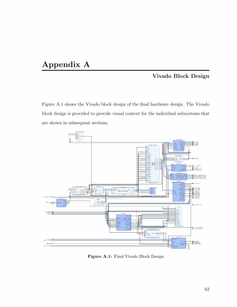
Appendix A
Vivado Block Design
Figure A.1 shows the Vivado block design of the final hardware design. The Vivado
block design is provided to provide visual context for the individual subsystems that
are shown in subsequent sections.
Figure A.1: Final Vivado Block Design
62
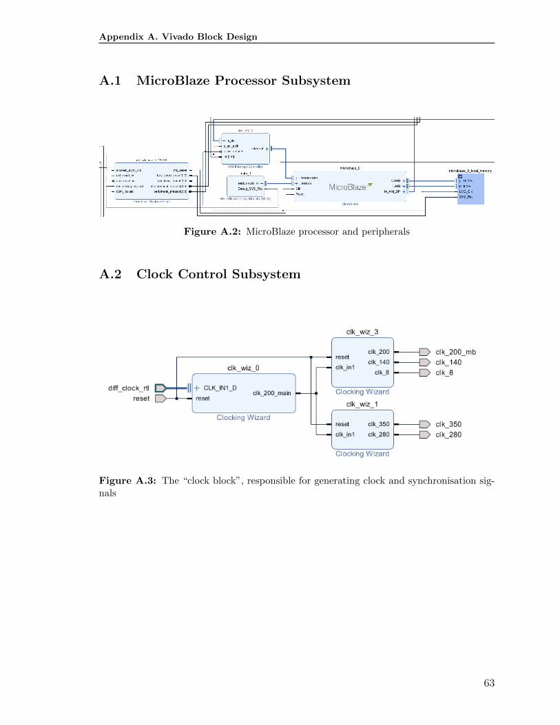
Appendix A. Vivado Block Design
A.1 MicroBlaze Processor Subsystem
Figure A.2: MicroBlaze processor and peripherals
A.2 Clock Control Subsystem
Figure A.3: The “clock block”, responsible for generating clock and synchronisation sig-nals
63
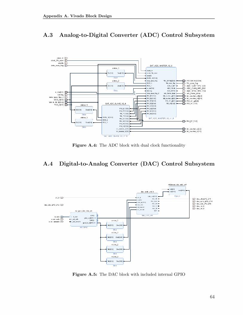
Appendix A. Vivado Block Design
A.3 Analog-to-Digital Converter (ADC) Control Subsystem
Figure A.4: The ADC block with dual clock functionality
A.4 Digital-to-Analog Converter (DAC) Control Subsystem
Figure A.5: The DAC block with included internal GPIO
64
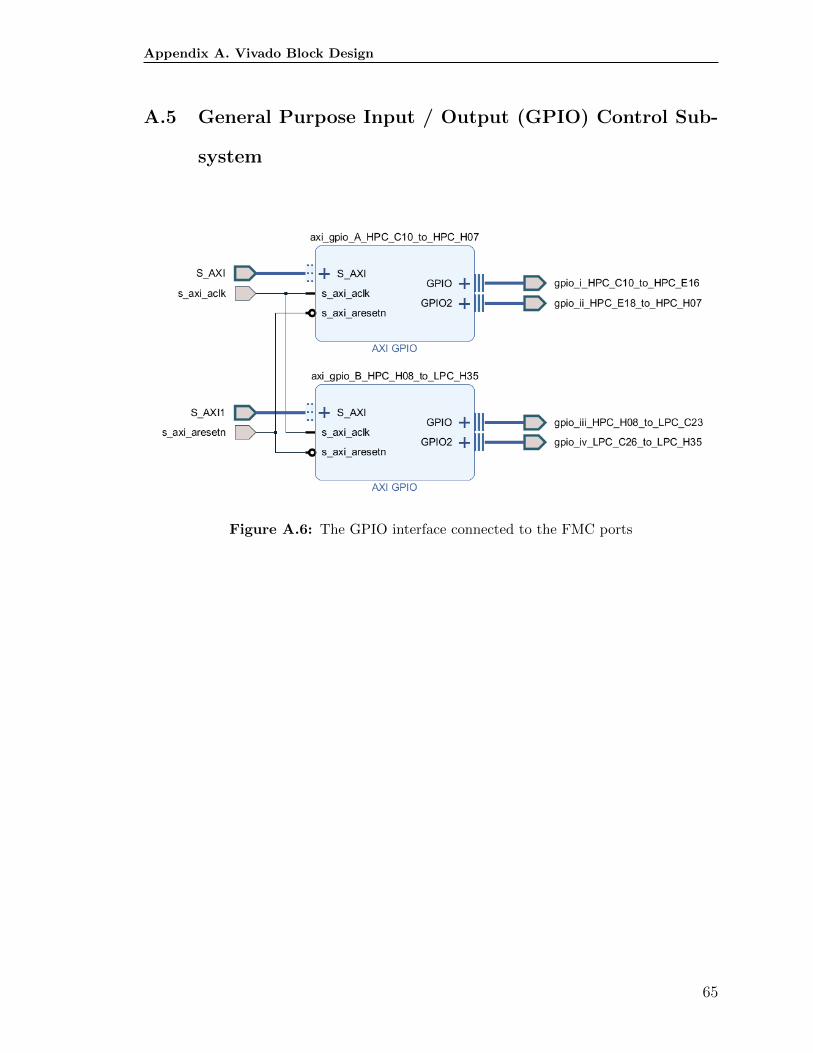
Appendix A. Vivado Block Design
A.5 General Purpose Input / Output (GPIO) Control Sub-
system
Figure A.6: The GPIO interface connected to the FMC ports
65
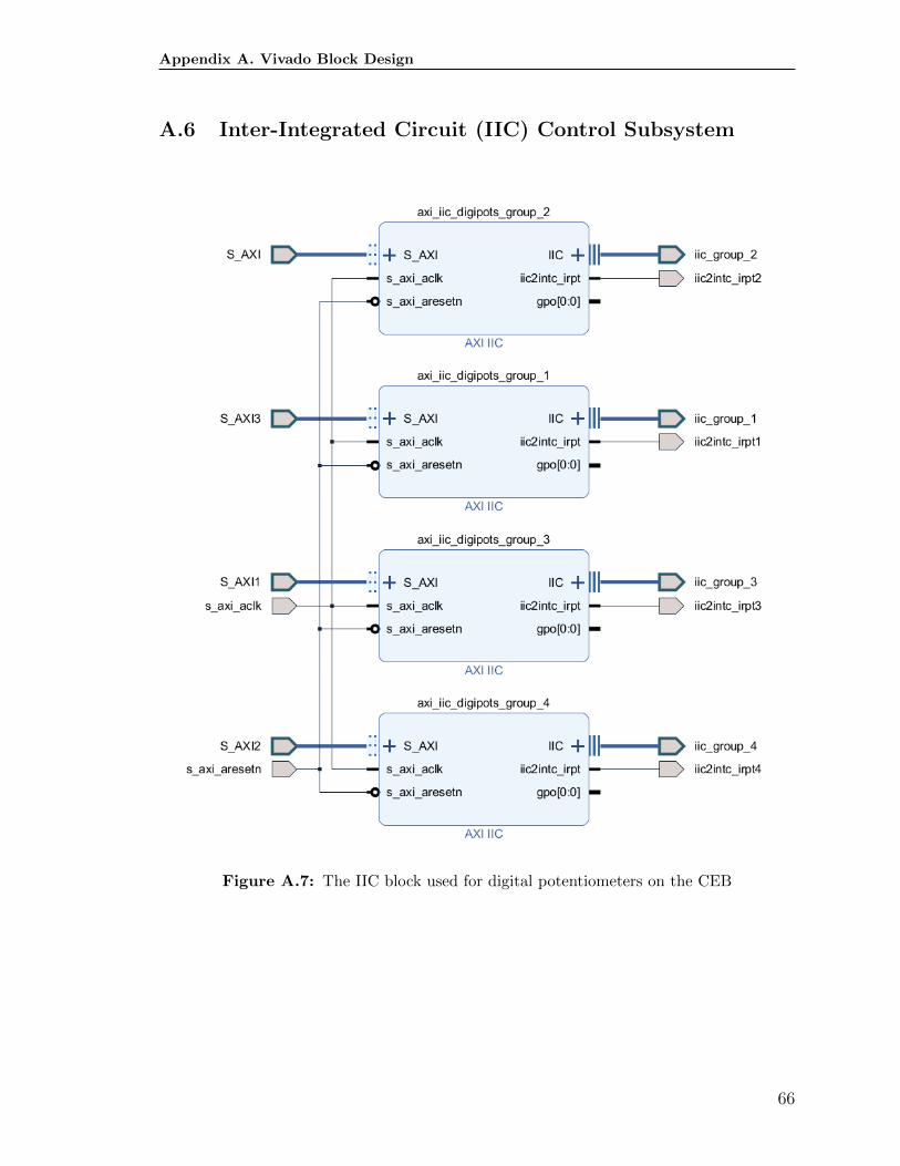
Appendix A. Vivado Block Design
A.6 Inter-Integrated Circuit (IIC) Control Subsystem
Figure A.7: The IIC block used for digital potentiometers on the CEB
66
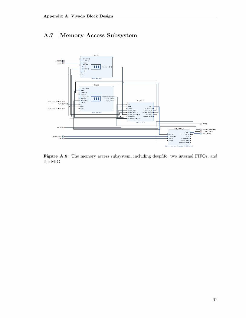
Appendix A. Vivado Block Design
A.7 Memory Access Subsystem
Figure A.8: The memory access subsystem, including deepfifo, two internal FIFOs, andthe MIG
67
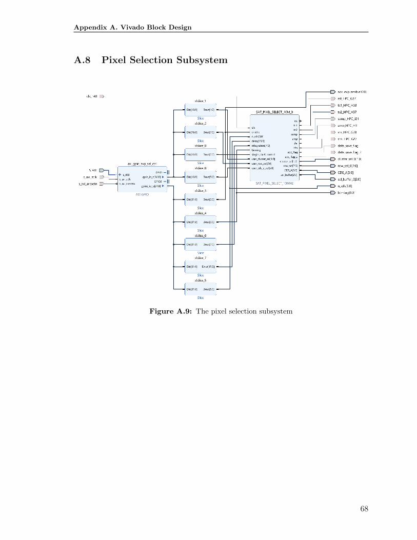
Appendix A. Vivado Block Design
A.8 Pixel Selection Subsystem
Figure A.9: The pixel selection subsystem
68