Magnetic Phase Diagram of Weakly Pinned Type-II Superconductors
Upload
independentCategory
view
0download
0
arX
iv:c
ond-
mat
/990
7310
v1 [
cond
-mat
.mtr
l-sc
i] 2
0 Ju
l 199
9
Instrumentation for Millimeter-wave Magnetoelectrodynamic Investigations of
Low-Dimensional Conductors and Superconductors
Monty Mola and Stephen Hill†
Department of Physics, Montana State University, Bozeman, MT 59717
Philippe Goy‡
AB Millimetre, 52 Rue Lhomond, 75005 Paris, France
Michel Gross§
Laboratoire KASTLER-BROSSEL, C.N.R.S. UMR 8552, and Universite Pierre-et-Marie Curie, Departement de Physique de
l’Ecole normale superieure, 24 Rue Lhomond, 75231 Paris, Cedex 05, France
(February 1, 2008)
We describe instrumentation for conducting high sensitivity millimeter-wave cavity perturbationmeasurements over a broad frequency range (40 − 200 GHz) and in the presence of strong magneticfields (up to 33 tesla). A Millimeter-wave Vector Network Analyzer (MVNA) acts as a continu-ously tunable microwave source and phase sensitive detector (8 − 350 GHz), enabling simultaneousmeasurements of the complex cavity parameters (resonance frequency and Q−value) at a rapid rep-etition rate (∼ 10 kHz). We discuss the principal of operation of the MVNA and the constructionof a probe for coupling the MVNA to various cylindrical resonator configurations which can easilybe inserted into a high field magnet cryostat. We also present several experimental results whichdemonstrate the potential of the instrument for studies of low-dimensional conducting systems.
I. Introduction
Anisotropy, or low-dimensionality, plays a fundamen-tal role in many areas of contemporary condensed matterphysics, both pure and applied. For example, much of thetechnology which has revolutionized the microelectronicsindustry in recent years has resulted from the develop-ment of low-dimensional semiconductor devices. Morerecently, research into bulk layered materials such asthe transition metal oxides,1 organic conductors,2 semi-conductor superlattices,3 magnetic nanostructures,4 etc.,has resulted in the discovery of a range of new physicalphenomena, e.g. high temperature superconductivity,5
colossal magnetoresistance,6 and a novel form of thequantum Hall effect.7 Many of these discoveries challengeour basic understanding of condensed matter physicswhile, at the same time, they hold the key to future tech-nologies.
The use of microwave techniques to probe the electro-dynamic properties of metals is not new. However, dueto recent interest in a range of novel conducting systemsin which the characteristic energy scales (e.g. electronicbandwidths, or energy gaps) coincide with the millimeterand sub-millimeter-wave spectral ranges, this field is un-dergoing a renaissance. Frequency dependent transportmeasurements in the presence of (strong) magnetic fields− the topic we call magnetoelectrodynamics, in analogyof magnetooptics − are expected to yield significant newinsights into the physics of low-dimensional conductors,just as conventional magnetooptics and magnetotrans-port measurements were essential decades ago in leadingto our present understanding of simple metals.
To date, few experiments on highly conducting mate-rials have combined high magnetic fields and millimeter-
wave spectroscopy.8 The reasons for this can be at-tributed to a range of factors. First, there are few com-mercially available sources and detectors working in thisfrequency range and those that can be used tend behighly priced, cumbersome to use, and possess either lowpower or an unstable output. Second, spectroscopy inthis frequency range is complex, particularly in the caseof metals: high sample reflectivity requires extreme sen-sitivity in order to detect small changes in conductivity;and the radiation wavelengths are typically larger thanavailable samples, thus rendering conventional reflectionspectroscopy useless. The inclusion of a magnetic fieldcomplicates these techniques considerably, since good op-tical coupling between the spectrometer (source and de-tector) and the sample under investigation is essential,and this is obviously difficult to achieve through the smallbore (comparable to λ) of a large magnet.
In this paper we describe instrumentation which hasbeen developed at Montana State University (MSU) forcarrying out sensitive spectroscopy of low-dimensionalconductors in the frequency range between 40 and 200GHz, and in magnetic fields up to 33 tesla which areavailable at the National High Magnetic Field Labora-tory (NHMFL) in Tallahassee, FL. In order to a) maxi-mize sensitivity, and b) achieve the required control overthe electromagnetic field distribution in the vicinity ofthe sample, we utilize an enclosed cavity perturbationtechnique (section II-B).8,9 The wide frequency cover-age and outstanding dynamic range (signal-to-noise) areachieved using a Millimeter-wave Vector Network Ana-lyzer (MVNA)10,11,12 as a source and detector (see sec-tion II-A). The resulting instrumentation offers uniqueexperimental possibilities in the area of metals physics in
1
high magnetic fields.The paper is organized as follows: section II contains
a detailed technical description of the system; in sectionIII, we discuss the performance of the instrument; andwe conclude with a summary of the paper in section IV.
II. TECHNICAL DESCRIPTION
A. The MVNA
As a source and detector, we employ a Millimeter-wave Vector Network Analyzer (MVNA)10,11,12 to mon-itor the phase and amplitude of millimeter-wave radi-ation transmitted through a resonant cavity containingthe sample under investigation. The MVNA 8-350, whichemploys purely solid-state electronics, allows measure-ments over an extended frequency range (8 - 350 GHz)13
through harmonic multiplication of a sweepable centime-ter source, S1, which provides a nominally flat outputpower in the range F1 = 8 - 18 GHz. The mm-wave sig-nal used in our experiments is extracted from a Shottkydiode (harmonic generator − HG) which has been opti-mized to produce the desired harmonic N of the sweep-able cm source, i.e. Fmm = N × F1. Detection is thenachieved by mixing the mm-wave signal (Fmm) with thesignal from a second cm source, S2, at a second Schot-tky diode (harmonic mixer − HM). The beat frequency,Fbeat, which preserves the phase and amplitude informa-tion of the mm-wave signal relative to the local oscillatorS2, is then sent to a heterodyne vector receiver (VR).
The low noise floor of the MVNA is achieved by defin-ing the frequency difference between the two cm sources,S1 and S2, using a main oscillator. If one then uses thesame harmonic rank on the source side (HG), and on thedetection side (HM), the phase noise associated with thecm sources cancels in the beat signal (Fbeat) which is sentto the VR. Thus, the phase reference of the VR can betaken directly from the main oscillator.14
With the noise characteristics of the analyzer opti-mized, its dynamic range is limited only by the harmonicconversion efficiency of the Schottky diodes. At MSU,three pairs of Schottky diodes are used, operating in theV (∼ 45 − 70 GHz, N = 3 and 4), W (70 − 110 GHz,N = 5 and 6) and D-bands (110− > 200 GHz, N = 7 to12). The V-band diodes are nominally flat broadband,while the W and D band diodes are mechanically tunableand require optimization each time the source frequency(F1) is changed. Operating in this mode, it is possibleto perform bench-top tests up to 350 GHz. Table I liststhe optimum dynamic ranges achieved at MSU (MVNA8 − 350 − 1 − 2)15 in each frequency band, and for eachharmonic, up to 200 GHz (N = 12). Similar analyzers arein use at several high magnetic field laboratories aroundthe world;16 in particular, the national magnet labs inthe US and The Netherlands have MVNA 8-350 analyz-ers (with ESA options)13 which are available to externalusers. The MVNA at the NHMFL, which has been usedfor some of the studies discussed in this paper, addition-ally operates in the Q (30− 50 GHz, N = 3), K (16− 32
GHz, N = 2) and X (8 − 18 GHz, N = 1) bands.Although the cm sources (S1 and S2) are phase (fre-
quency) locked to each other, their absolute frequen-cies must be stabilized also. The frequency precisionand stability provided by the MVNA 8-350 is not ade-quate for narrow-band cavity perturbation measurementswhen the bandwidth of the cavity is less than about 100MHz. For this reason, it is common to phase-lock oneof the sources (i.e. both) to a quartz standard. At MSUand at the NHMFL, EIP 575 source-locking frequencycounters17 are used, which provide both the stability andprecision necessary for the measurements described inthis paper. One other mode of operation involves phaselocking the source (S1) directly to the high−Q cavity res-onator used for the experiment. The counter is also usefulin this case for recording changes in frequency resultingfrom any changes in dispersion within the cavity. Com-parisons between the two frequency locking techniquesare discussed in section III-B.
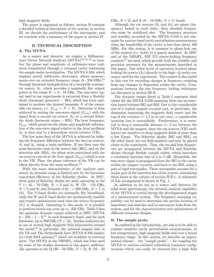
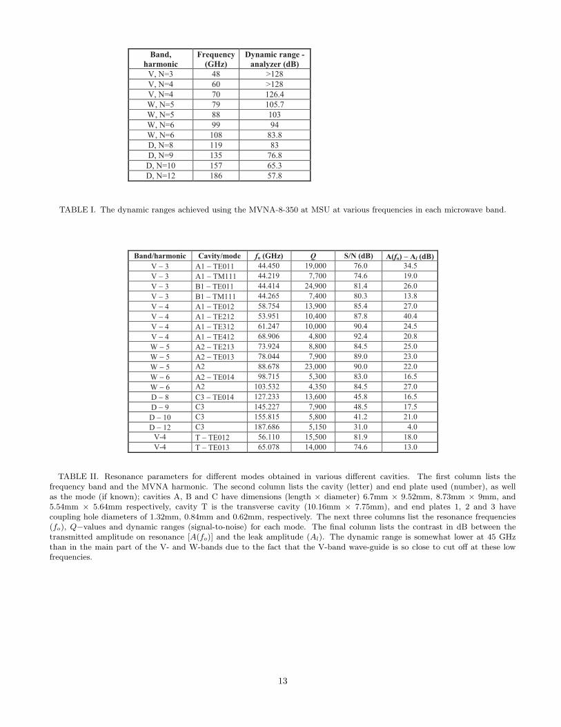
The dynamic ranges listed in Table I represent idealvalues for the MVNA 8-350 assuming there are no inser-tion losses between HG and HM. Due to the considerablesize of a typical magnet cryostat and, in particular, thedimension separating the magnetic field center and thetop of the cryostat (∼ 1.5 m in our case), a considerableinsertion loss is unavoidable. Furthermore, it is essen-tial to keep a reasonable distance (∼ 2 m) between theMVNA and the magnet, since the cm sources (YIG oscil-lators) are sensitive to stray magnetic fields of more thana few Gauss. The Schottky diodes (HG and HM), onthe other hand, are not field sensitive and may be placedcloser to the experiment. Thus, the cm and beat frequen-cies are propagated between the MVNA and Schottkydiodes through flexible coaxial cables, which introducea combined insertion loss of 4 to 5 dB. Meanwhile, themm-wave signal is propagated from the HG to the cavitywithin the magnet cryostat, and back to the HM, using apair of rigid waveguides. These waveguides account for amajor part of the insertion loss of the system; minimizingthese losses is the subject of section II-B.1. A schematicof this arrangement is shown in Fig. 1.
In addition to its use as a source and detector forsolid state spectroscopy, the network analysis capabilityof the MVNA is crucial during the developmental stagesof a measurement system. The frequency sweeping ca-pability can be used to determine the precise location ofimpedance mis-matches and/or microwave leaks from thesystem, and for the characterization and optimization ofdifferent resonator designs.
B. The sample probe
As outlined in the introduction, our aim is to be able toconduct sensitive cavity perturbation measurements, atlow temperatures, high magnetic fields and over a broadfrequency range. In this section, we describe an experi-mental scheme − the ”sample probe” − for coupling theMVNA to various enclosed cylindrical resonator config-urations which can easily be inserted into a high field
2
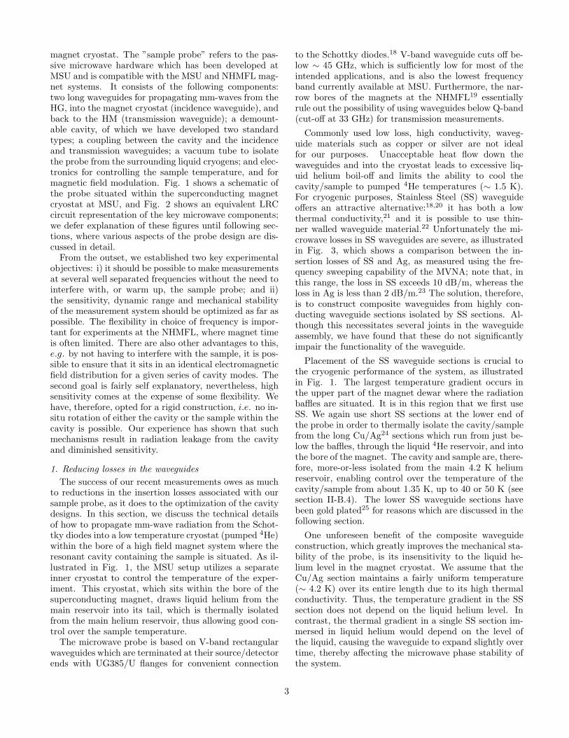
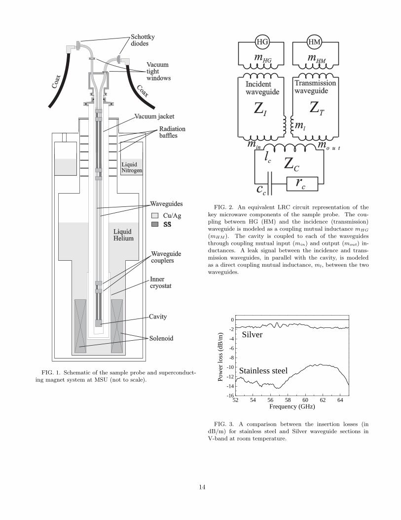
magnet cryostat. The ”sample probe” refers to the pas-sive microwave hardware which has been developed atMSU and is compatible with the MSU and NHMFL mag-net systems. It consists of the following components:two long waveguides for propagating mm-waves from theHG, into the magnet cryostat (incidence waveguide), andback to the HM (transmission waveguide); a demount-able cavity, of which we have developed two standardtypes; a coupling between the cavity and the incidenceand transmission waveguides; a vacuum tube to isolatethe probe from the surrounding liquid cryogens; and elec-tronics for controlling the sample temperature, and formagnetic field modulation. Fig. 1 shows a schematic ofthe probe situated within the superconducting magnetcryostat at MSU, and Fig. 2 shows an equivalent LRCcircuit representation of the key microwave components;we defer explanation of these figures until following sec-tions, where various aspects of the probe design are dis-cussed in detail.
From the outset, we established two key experimentalobjectives: i) it should be possible to make measurementsat several well separated frequencies without the need tointerfere with, or warm up, the sample probe; and ii)the sensitivity, dynamic range and mechanical stabilityof the measurement system should be optimized as far aspossible. The flexibility in choice of frequency is impor-tant for experiments at the NHMFL, where magnet timeis often limited. There are also other advantages to this,e.g. by not having to interfere with the sample, it is pos-sible to ensure that it sits in an identical electromagneticfield distribution for a given series of cavity modes. Thesecond goal is fairly self explanatory, nevertheless, highsensitivity comes at the expense of some flexibility. Wehave, therefore, opted for a rigid construction, i.e. no in-situ rotation of either the cavity or the sample within thecavity is possible. Our experience has shown that suchmechanisms result in radiation leakage from the cavityand diminished sensitivity.
1. Reducing losses in the waveguides
The success of our recent measurements owes as muchto reductions in the insertion losses associated with oursample probe, as it does to the optimization of the cavitydesigns. In this section, we discuss the technical detailsof how to propagate mm-wave radiation from the Schot-tky diodes into a low temperature cryostat (pumped 4He)within the bore of a high field magnet system where theresonant cavity containing the sample is situated. As il-lustrated in Fig. 1, the MSU setup utilizes a separateinner cryostat to control the temperature of the exper-iment. This cryostat, which sits within the bore of thesuperconducting magnet, draws liquid helium from themain reservoir into its tail, which is thermally isolatedfrom the main helium reservoir, thus allowing good con-trol over the sample temperature.
The microwave probe is based on V-band rectangularwaveguides which are terminated at their source/detectorends with UG385/U flanges for convenient connection
to the Schottky diodes.18 V-band waveguide cuts off be-low ∼ 45 GHz, which is sufficiently low for most of theintended applications, and is also the lowest frequencyband currently available at MSU. Furthermore, the nar-row bores of the magnets at the NHMFL19 essentiallyrule out the possibility of using waveguides below Q-band(cut-off at 33 GHz) for transmission measurements.
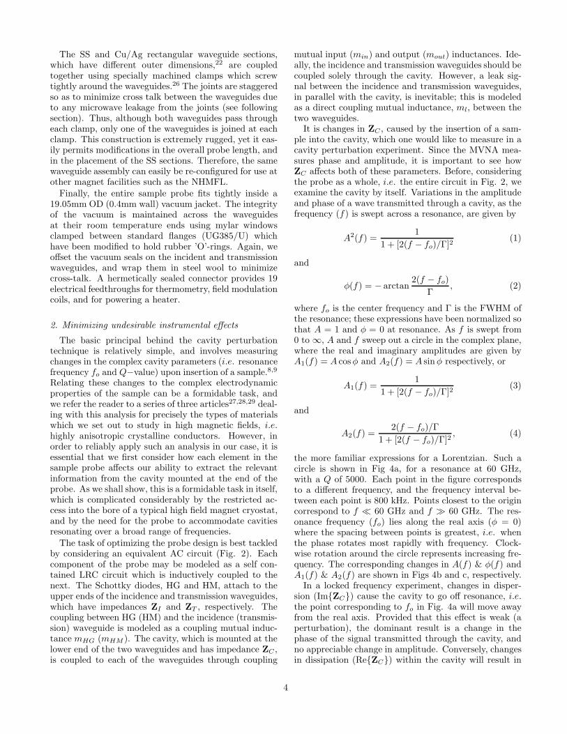
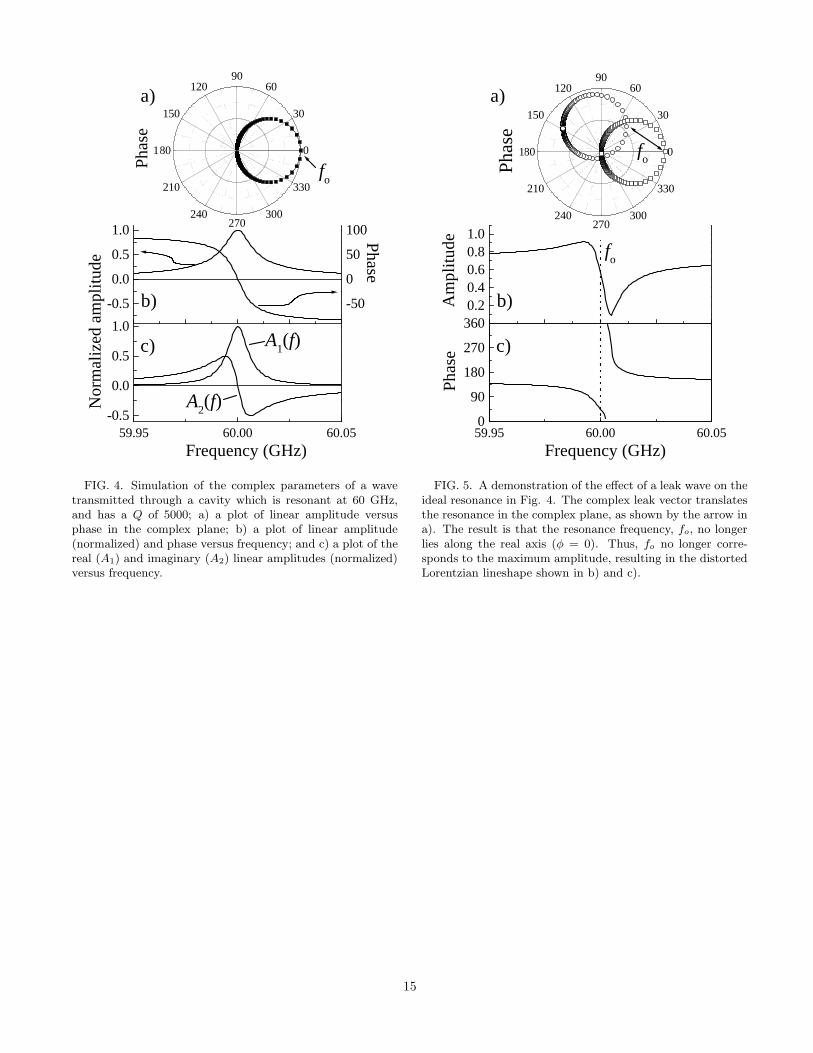
Commonly used low loss, high conductivity, waveg-uide materials such as copper or silver are not idealfor our purposes. Unacceptable heat flow down thewaveguides and into the cryostat leads to excessive liq-uid helium boil-off and limits the ability to cool thecavity/sample to pumped 4He temperatures (∼ 1.5 K).For cryogenic purposes, Stainless Steel (SS) waveguideoffers an attractive alternative:18,20 it has both a lowthermal conductivity,21 and it is possible to use thin-ner walled waveguide material.22 Unfortunately the mi-crowave losses in SS waveguides are severe, as illustratedin Fig. 3, which shows a comparison between the in-sertion losses of SS and Ag, as measured using the fre-quency sweeping capability of the MVNA; note that, inthis range, the loss in SS exceeds 10 dB/m, whereas theloss in Ag is less than 2 dB/m.23 The solution, therefore,is to construct composite waveguides from highly con-ducting waveguide sections isolated by SS sections. Al-though this necessitates several joints in the waveguideassembly, we have found that these do not significantlyimpair the functionality of the waveguide.
Placement of the SS waveguide sections is crucial tothe cryogenic performance of the system, as illustratedin Fig. 1. The largest temperature gradient occurs inthe upper part of the magnet dewar where the radiationbaffles are situated. It is in this region that we first useSS. We again use short SS sections at the lower end ofthe probe in order to thermally isolate the cavity/samplefrom the long Cu/Ag24 sections which run from just be-low the baffles, through the liquid 4He reservoir, and intothe bore of the magnet. The cavity and sample are, there-fore, more-or-less isolated from the main 4.2 K heliumreservoir, enabling control over the temperature of thecavity/sample from about 1.35 K, up to 40 or 50 K (seesection II-B.4). The lower SS waveguide sections havebeen gold plated25 for reasons which are discussed in thefollowing section.
One unforeseen benefit of the composite waveguideconstruction, which greatly improves the mechanical sta-bility of the probe, is its insensitivity to the liquid he-lium level in the magnet cryostat. We assume that theCu/Ag section maintains a fairly uniform temperature(∼ 4.2 K) over its entire length due to its high thermalconductivity. Thus, the temperature gradient in the SSsection does not depend on the liquid helium level. Incontrast, the thermal gradient in a single SS section im-mersed in liquid helium would depend on the level ofthe liquid, causing the waveguide to expand slightly overtime, thereby affecting the microwave phase stability ofthe system.
3
The SS and Cu/Ag rectangular waveguide sections,which have different outer dimensions,22 are coupledtogether using specially machined clamps which screwtightly around the waveguides.26 The joints are staggeredso as to minimize cross talk between the waveguides dueto any microwave leakage from the joints (see followingsection). Thus, although both waveguides pass througheach clamp, only one of the waveguides is joined at eachclamp. This construction is extremely rugged, yet it eas-ily permits modifications in the overall probe length, andin the placement of the SS sections. Therefore, the samewaveguide assembly can easily be re-configured for use atother magnet facilities such as the NHMFL.
Finally, the entire sample probe fits tightly inside a19.05mm OD (0.4mm wall) vacuum jacket. The integrityof the vacuum is maintained across the waveguidesat their room temperature ends using mylar windowsclamped between standard flanges (UG385/U) whichhave been modified to hold rubber ’O’-rings. Again, weoffset the vacuum seals on the incident and transmissionwaveguides, and wrap them in steel wool to minimizecross-talk. A hermetically sealed connector provides 19electrical feedthroughs for thermometry, field modulationcoils, and for powering a heater.
2. Minimizing undesirable instrumental effects
The basic principal behind the cavity perturbationtechnique is relatively simple, and involves measuringchanges in the complex cavity parameters (i.e. resonancefrequency fo and Q−value) upon insertion of a sample.8,9
Relating these changes to the complex electrodynamicproperties of the sample can be a formidable task, andwe refer the reader to a series of three articles27,28,29 deal-ing with this analysis for precisely the types of materialswhich we set out to study in high magnetic fields, i.e.highly anisotropic crystalline conductors. However, inorder to reliably apply such an analysis in our case, it isessential that we first consider how each element in thesample probe affects our ability to extract the relevantinformation from the cavity mounted at the end of theprobe. As we shall show, this is a formidable task in itself,which is complicated considerably by the restricted ac-cess into the bore of a typical high field magnet cryostat,and by the need for the probe to accommodate cavitiesresonating over a broad range of frequencies.
The task of optimizing the probe design is best tackledby considering an equivalent AC circuit (Fig. 2). Eachcomponent of the probe may be modeled as a self con-tained LRC circuit which is inductively coupled to thenext. The Schottky diodes, HG and HM, attach to theupper ends of the incidence and transmission waveguides,which have impedances ZI and ZT , respectively. Thecoupling between HG (HM) and the incidence (transmis-sion) waveguide is modeled as a coupling mutual induc-tance mHG (mHM ). The cavity, which is mounted at thelower end of the two waveguides and has impedance ZC ,is coupled to each of the waveguides through coupling
mutual input (min) and output (mout) inductances. Ide-ally, the incidence and transmission waveguides should becoupled solely through the cavity. However, a leak sig-nal between the incidence and transmission waveguides,in parallel with the cavity, is inevitable; this is modeledas a direct coupling mutual inductance, ml, between thetwo waveguides.
It is changes in ZC , caused by the insertion of a sam-ple into the cavity, which one would like to measure in acavity perturbation experiment. Since the MVNA mea-sures phase and amplitude, it is important to see howZC affects both of these parameters. Before, consideringthe probe as a whole, i.e. the entire circuit in Fig. 2, weexamine the cavity by itself. Variations in the amplitudeand phase of a wave transmitted through a cavity, as thefrequency (f) is swept across a resonance, are given by
A2(f) =1
1 + [2(f − fo)/Γ]2(1)
and
φ(f) = − arctan2(f − fo)
Γ, (2)
where fo is the center frequency and Γ is the FWHM ofthe resonance; these expressions have been normalized sothat A = 1 and φ = 0 at resonance. As f is swept from0 to ∞, A and f sweep out a circle in the complex plane,where the real and imaginary amplitudes are given byA1(f) = A cosφ and A2(f) = A sin φ respectively, or
A1(f) =1
1 + [2(f − fo)/Γ]2(3)
and
A2(f) =2(f − fo)/Γ
1 + [2(f − fo)/Γ]2, (4)
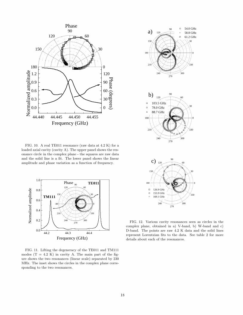
the more familiar expressions for a Lorentzian. Such acircle is shown in Fig 4a, for a resonance at 60 GHz,with a Q of 5000. Each point in the figure correspondsto a different frequency, and the frequency interval be-tween each point is 800 kHz. Points closest to the origincorrespond to f ≪ 60 GHz and f ≫ 60 GHz. The res-onance frequency (fo) lies along the real axis (φ = 0)where the spacing between points is greatest, i.e. whenthe phase rotates most rapidly with frequency. Clock-wise rotation around the circle represents increasing fre-quency. The corresponding changes in A(f) & φ(f) andA1(f) & A2(f) are shown in Figs 4b and c, respectively.
In a locked frequency experiment, changes in disper-sion (ImZC) cause the cavity to go off resonance, i.e.the point corresponding to fo in Fig. 4a will move awayfrom the real axis. Provided that this effect is weak (aperturbation), the dominant result is a change in thephase of the signal transmitted through the cavity, andno appreciable change in amplitude. Conversely, changesin dissipation (ReZC) within the cavity will result in
4

a reduction in the amplitude of the signal transmittedthrough the cavity and, hence, a reduction in the diam-eter of the circle in Fig. 4a. Dissipation alone does notmove fo away from the real axis and, therefore, does notaffect the phase of the wave. However, dispersion canaffect both the amplitude and the phase of the wave iffo moves appreciably off the real axis. For this reason, itis often desirable to conduct a locked phase experiment,which completely decouples these two effects. With aphase lock, the cavity stays on resonance (on the realaxis in Fig. 4a), and dispersion affects the resonancefrequency only, which we can measure with a frequencycounter. Meanwhile, changes in dissipation again affectthe amplitude of the transmitted signal only.
Unfortunately, each of the additional circuit elementsrequired to link the MVNA to the cavity, and/or im-proper coupling between these components, has the po-tential to seriously distort the simple relationships be-tween dissipation, dispersion, amplitude and phase dis-cussed above. Ideally, the sample probe should be pas-sive, low loss, insensitive to temperature and magneticfield and, with the exception of the cavity, should have aflat broad-band frequency response. In practice, this isnever actually possible to achieve. Nevertheless, by con-ducting a thorough characterization and optimization ofeach element in the microwave circuit (Fig. 2), it is pos-sible to minimize these instrumental effects to negligiblelevels. The MVNA performs a pivotal role in this hard-ware developmental process. The following paragraphsdiscuss various undesirable instrumental characteristics,their potential effect on a measurement, and the steps wehave taken to eliminate these sources of error.
A leak wave bypassing the cavity directly throughto the transmission waveguide has two adverse effects.First, it diminishes the useful dynamic range − ideally100% of the signal reaching the detector should passthrough the cavity. Second, if the leak amplitude is com-parable to the amplitude of the signal passing throughthe cavity, the resonance may become severely distorted,making it extremely difficult to distinguish between dis-sipative and dispersive effects within the cavity. As il-lustrated in Fig. 5, a leak wave adds a complex vectorto the signal transmitted through the cavity. By mini-mizing the leak, one can control its amplitude. However,it is not possible to control the phase of the leak wave.Consequently, big leaks lead to an arbitrary vector trans-lation of the circle in Fig. 4a; this is a pure translation,i.e. each point on the circle is translated by the samevector. Hence, the line joining the resonance frequency,fo, and the f = 0 & ∞ points, remains parallel to thereal axis. As a result, the transmitted amplitude on reso-nance is not necessarily the maximum amplitude; indeed,it can take on any value from zero to one plus the leakamplitude. This is illustrated in Fig. 5 for an arbitrarytranslation of the circle in Fig. 4a, together with thecorresponding variations in phase and amplitude, plot-ted versus frequency. It is apparent from this figure that
the phase of the leak signal is entirely responsible for theway in which dissipation and dispersion affect the phaseand amplitude of the signal transmitted through the cav-ity. Thus, an appreciable leak signal is intolerable, andwe have taken every step to reduce the leak in our probeto at least 20 dB below the typical signal transmittedthrough the cavity on resonance, as discussed above.
Standing waves in the waveguides are unavoidableand, without proper attention, can cause considerableproblems, especially when operating in the phase-lockedmode in which the incident mm-wave frequency is lockedto the cavity resonance frequency. Changes in this fre-quency will result in changes in the phase and amplitudeof the mm-wave signal incident upon the cavity. Thus, itbecomes impossible to distinguish between the intrinsiccavity response and spurious effects due to the standingwaves. Furthermore, the phase is no longer truly lockedto the cavity resonance under these circumstances, butrather to the coupled response of the entire circuit in Fig.2. Standing waves should not be ignored altogether inthe frequency locked mode either, particularly when thecavity is well coupled to the waveguides. Under thesecircumstances, changes in ZC influence the impedancematching between the cavity and the waveguides (i.e.min and mout) and, therefore, affect the standing waves.
There is little to be gained from trying to eliminatethe standing waves completely. This would require pre-cise impedance matching of each component in Fig. 2,which is only possible to achieve over a narrow frequencyrange and would, therefore, defeat the purpose of theprobe, which is intended to work over a fairly broad fre-quency range. Instead, we concentrate on minimizing theinfluence of the standing waves on a measurement at anygiven frequency. This is achieved by reducing the fre-quency bandwidth of the measurement to well below theperiodicity of the standing wave pattern, i.e. so that theresponse of the waveguides is essentially flat over the rel-evant frequency interval. In this way, a range of cavitiesor cavity modes may be utilized, covering an extremelybroad frequency range in comparison to the standingwave periodicity. Meanwhile, each cavity mode samplesonly a minute portion of the waveguide spectrum, overwhich its response is essentially flat.
The fastest standing wave period is governed by thelongest dimension of the sample probe, which is 3m inour case (HG to HM, via the cavity). This gives rise toa standing wave periodicity of about 100 MHz which, inturn, requires cavity filling factors of less than 10−4, sothat the frequency shift in any given measurement neverexceeds about 10−4 of the measurement frequency, i.e.∆fo < 10 MHz for f < 100 GHz. Cavity filling fac-tors of between 10−5 and 10−4 are typical for the typesof samples we study, so standing wave problems do notforce this restriction upon us. Nevertheless, to compen-sate for the small filling factors, it is essential to havecavity Q−factors on the order of 104. In order to at-tain such high Q−values, the cavity must necessarily be
5
coupled weakly to the waveguides, which further reducesproblems associated with standing waves.
Phase instability, and/or a strong frequency depen-dence of the phase reaching the VR, can lead to a va-riety of problems. Although the internal sources withinthe MVNA are phase locked, additional phase jitter canarise in the mm-wave signal due to mechanical and/orthermal instabilities in the sample probe. Mechanical vi-brations do not pose any problems, either at MSU or atthe NHMFL. However, thermal stability is essential forachieving the best results. Due to extremely high cavityQ−values, minor temperature fluctuations can lead tosignificant phase instabilities, particularly when study-ing samples with a strongly temperature dependent elec-trodynamic response. For this reason, active tempera-ture control is necessary (see section II-B.4). Long termthermal stability of the entire probe, including the 1.5mwaveguide sections, is also desirable and is best achievedusing the composite waveguides described in the previoussection.
A strong frequency dependence of the phase reachingthe VR occurs when the distances between the sources S1
and S2 and the HM are very different. The signal origi-nating at S1 has to travel the extra 2 × 1.5 m into, andout of, the magnet cryostat. For this reason, it can bebeneficial to compensate for the extra distance betweenS1 and the HM by adding 3 m of coaxial cable30 betweenS2 and the HM, especially when performing phase-lockedor frequency swept measurements, even though this in-troduces an extra 2 − 3 dB insertion loss.
Spurious magnetic resonances caused by paramag-netic contamination of either the cavity, or the waveg-uides close to the magnetic field center, will give riseto both sharp and broad instrumental features (Elec-tron Paramagnetic Resonances - EPR) in the transmis-sion versus magnetic field response of the system. Thesespurious resonances can be hard to distinguish from thegenuine response of the sample within the cavity, andshould be eliminated so that the magnetic field responseof the unloaded probe (i.e. with no sample) is as flatas possible. The SS waveguide sections cause the mostsevere problems, which we suspect is due to the presenceof small traces of Fe3+ (rust) at the surface of the metal.For this reason, we have gold plated the SS sections whichcouple directly to the cavity. This not only reduces theinsertion loss due to these sections, but also completelyeliminates a broad instrumental resonance, leaving an ex-tremely flat response (∆A < 0.05 dB), as shown in Fig.6. A number of other measures have been taken to avoidcontaminating the lower end of the probe (i.e. close tothe field center) with paramagnetic impurities. These in-clude clamping all components together rather than us-ing adhesives or solders, and avoiding the use of cuttingoils when machining the resonators. We have also goldplated some of the cavities to prevent tarnishing. Nev-ertheless, electrolytic OFHC Cu cavities work extremelywell without plating (see Fig. 6).
3. The cavities
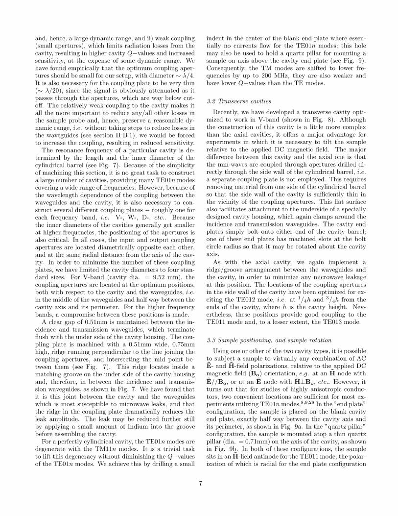
To date, our efforts have focussed on the use of en-closed cylindrical resonators for cavity perturbation mea-surements. There are several compelling reasons to doso. To begin with, the simple design concept we havedeveloped, in which the cavities are assembled from rel-atively few easily machinable components (see Figs. 7and 8), enables us to fabricate a range of cavities and,therefore, switch frequency range/coverage with relativeease.31 More importantly, relative to rectangular cavities,it is straightforward to achieve extremely high Q−values(> 104) for the TE01n (n = 1, 2, 3...) modes of cylindricalresonators. The reason for this has to do with the factthat no AC currents flow between the end and side wallsof a cylindrical cavity excited in its TE01n mode. Conse-quently, joints at these ideal locations (see Figs 7 and 8)do not diminish the cavity Q−factor. These modes alsopossess electromagnetic field geometries which are highlydesirable for the measurements described in this paper.
3.1. Axial cavities
For the most part, we use axial cavities of the typeshown in Fig. 7, i.e. ones in which the cavity axis iscoincident with the axis of the superconducting solenoid.This is by far the most versatile design, though it doeshave some limitations, especially when it is necessary totilt the sample with respect to the applied DC magneticfield. The cavity is constructed from OFHC electrolyticcopper in three pieces - a blank end plate, a couplingplate and a cylindrical barrel. This assembly bolts ontothe under side of a copper housing which clamps aroundthe incidence and transmission waveguides. These boltsalso provide the pressure for reproducibly clamping thecavity assembly tightly together; no adhesives or sol-ders are used. The cavity may be disconnected from thewaveguides in a matter of seconds for easy sample in-sertion/removal. The housing which clamps around thewaveguides is also easily interchanged with a separatehousing for a transverse cylindrical cavity (see below).
Coupling between the waveguides and the cavity isachieved by means of small circular apertures in the thincoupling plates. Since these plates terminate the waveg-uides and the cavity, there are no transverse microwaveelectric (E-) fields at the locations of the apertures. Thus,
it is the microwave magnetic (H-) fields in the waveguidesand the cavity which should be matched. For the TE01nmodes, the H-fields flow radially at the cavity ends and,therefore, the H-fields in the waveguides should do soalso. For this reason, the incoming waveguides are ori-ented with their shortest edges closest together (see Figs1, 7 and 8).32
We can control the degree of coupling between thewaveguides and the cavity (min and mout) by meansof the dimensions of the coupling apertures (diameterand thickness). There is an important trade off here be-tween i) strong coupling (large apertures), which ensuresgood power throughput from the source to the detector
6
and, hence, a large dynamic range, and ii) weak coupling(small apertures), which limits radiation losses from thecavity, resulting in higher cavity Q−values and increasedsensitivity, at the expense of some dynamic range. Wehave found empirically that the optimum coupling aper-tures should be small for our setup, with diameter ∼ λ/4.It is also necessary for the coupling plate to be very thin(∼ λ/20), since the signal is obviously attenuated as itpasses through the apertures, which are way below cut-off. The relatively weak coupling to the cavity makes itall the more important to reduce any/all other losses inthe sample probe and, hence, preserve a reasonable dy-namic range, i.e. without taking steps to reduce losses inthe waveguides (see section II-B.1), we would be forcedto increase the coupling, resulting in reduced sensitivity.
The resonance frequency of a particular cavity is de-termined by the length and the inner diameter of thecylindrical barrel (see Fig. 7). Because of the simplicityof machining this section, it is no great task to constructa large number of cavities, providing many TE01n modescovering a wide range of frequencies. However, because ofthe wavelength dependence of the coupling between thewaveguides and the cavity, it is also necessary to con-struct several different coupling plates − roughly one foreach frequency band, i.e. V-, W-, D-, etc.. Becausethe inner diameters of the cavities generally get smallerat higher frequencies, the positioning of the apertures isalso critical. In all cases, the input and output couplingapertures are located diametrically opposite each other,and at the same radial distance from the axis of the cav-ity. In order to minimize the number of these couplingplates, we have limited the cavity diameters to four stan-dard sizes. For V-band (cavity dia. = 9.52 mm), thecoupling apertures are located at the optimum positions,both with respect to the cavity and the waveguides, i.e.in the middle of the waveguides and half way between thecavity axis and its perimeter. For the higher frequencybands, a compromise between these positions is made.
A clear gap of 0.51mm is maintained between the in-cidence and transmission waveguides, which terminateflush with the under side of the cavity housing. The cou-pling plate is machined with a 0.51mm wide, 0.75mmhigh, ridge running perpendicular to the line joining thecoupling apertures, and intersecting the mid point be-tween them (see Fig. 7). This ridge locates inside amatching groove on the under side of the cavity housingand, therefore, in between the incidence and transmis-sion waveguides, as shown in Fig. 7. We have found thatit is this joint between the cavity and the waveguideswhich is most susceptible to microwave leaks, and thatthe ridge in the coupling plate dramatically reduces theleak amplitude. The leak may be reduced further stillby applying a small amount of Indium into the groovebefore assembling the cavity.
For a perfectly cylindrical cavity, the TE01n modes aredegenerate with the TM11n modes. It is a trivial taskto lift this degeneracy without diminishing the Q−valuesof the TE01n modes. We achieve this by drilling a small
indent in the center of the blank end plate where essen-tially no currents flow for the TE01n modes; this holemay also be used to hold a quartz pillar for mounting asample on axis above the cavity end plate (see Fig. 9).Consequently, the TM modes are shifted to lower fre-quencies by up to 200 MHz, they are also weaker andhave lower Q−values than the TE modes.
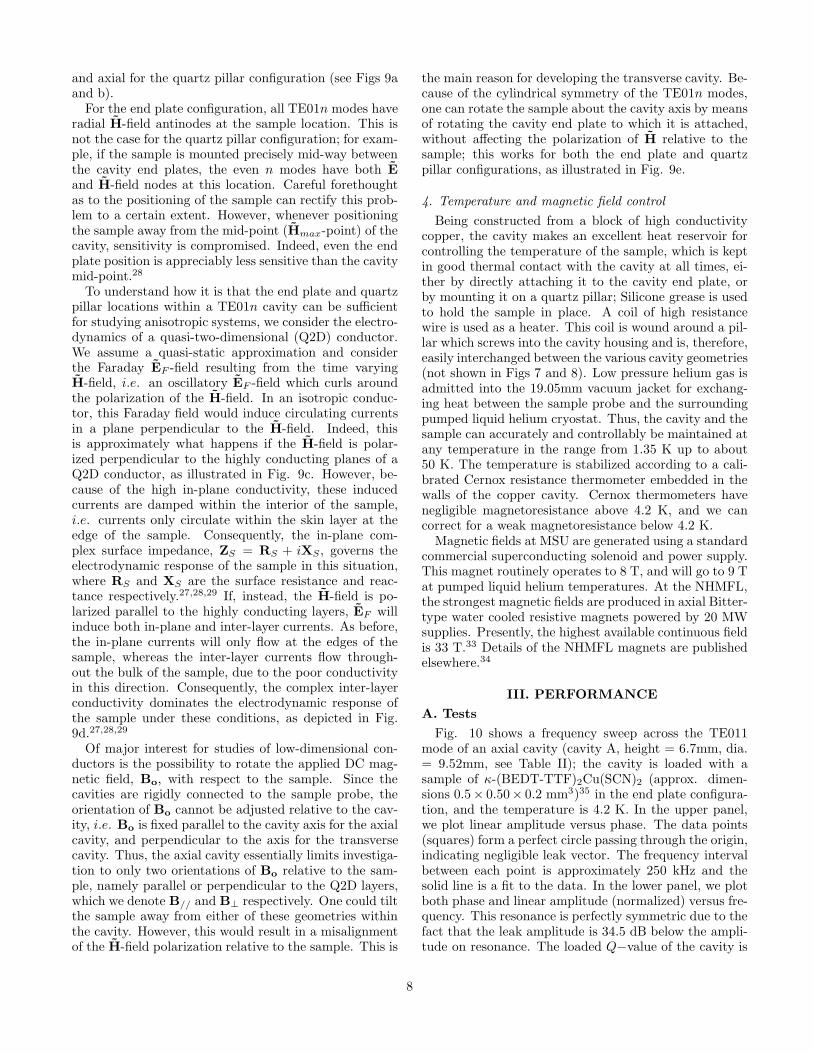
3.2 Transverse cavities
Recently, we have developed a transverse cavity opti-mized to work in V-band (shown in Fig. 8). Althoughthe construction of this cavity is a little more complexthan the axial cavities, it offers a major advantage forexperiments in which it is necessary to tilt the samplerelative to the applied DC magnetic field. The majordifference between this cavity and the axial one is thatthe mm-waves are coupled through apertures drilled di-rectly through the side wall of the cylindrical barrel, i.e.a separate coupling plate is not employed. This requiresremoving material from one side of the cylindrical barrelso that the side wall of the cavity is sufficiently thin inthe vicinity of the coupling apertures. This flat surfacealso facilitates attachment to the underside of a speciallydesigned cavity housing, which again clamps around theincidence and transmission waveguides. The cavity endplates simply bolt onto either end of the cavity barrel;one of these end plates has machined slots at the boltcircle radius so that it may be rotated about the cavityaxis.
As with the axial cavity, we again implement aridge/groove arrangement between the waveguides andthe cavity, in order to minimize any microwave leakageat this position. The locations of the coupling aperturesin the side wall of the cavity have been optimized for ex-citing the TE012 mode, i.e. at 1/4h and 3/4h from theends of the cavity, where h is the cavity height. Nev-ertheless, these positions provide good coupling to theTE011 mode and, to a lesser extent, the TE013 mode.
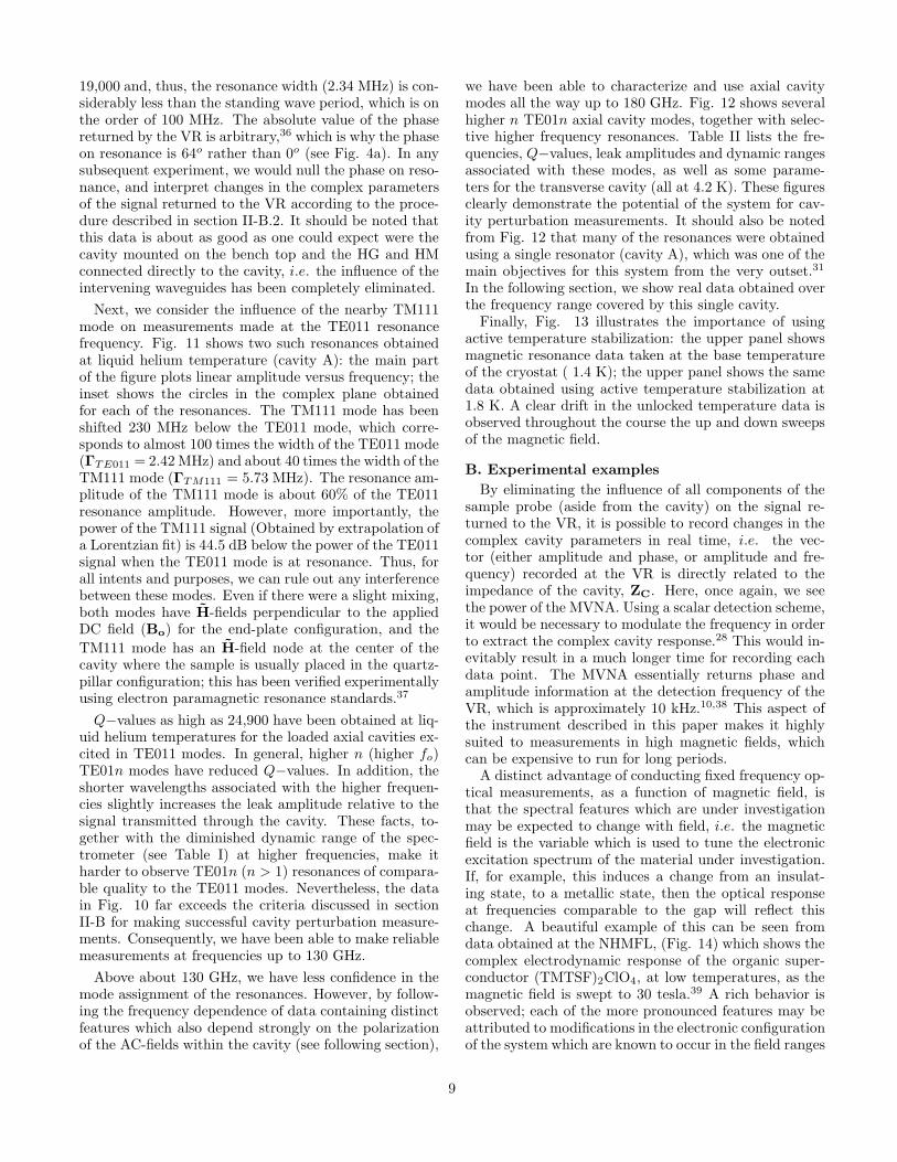
3.3 Sample positioning, and sample rotation
Using one or other of the two cavity types, it is possibleto subject a sample to virtually any combination of ACE- and H-field polarizations, relative to the applied DCmagnetic field (Bo) orientation, e.g. at an H node with
E//Bo, or at an E node with H⊥Bo, etc.. However, itturns out that for studies of highly anisotropic conduc-tors, two convenient locations are sufficient for most ex-periments utilizing TE01n modes.8,9,28 In the ”end plate”configuration, the sample is placed on the blank cavityend plate, exactly half way between the cavity axis andits perimeter, as shown in Fig. 9a. In the ”quartz pillar”configuration, the sample is mounted atop a thin quartzpillar (dia. = 0.71mm) on the axis of the cavity, as shownin Fig. 9b. In both of these configurations, the samplesits in an H-field antinode for the TE011 mode, the polar-ization of which is radial for the end plate configuration
7
and axial for the quartz pillar configuration (see Figs 9aand b).
For the end plate configuration, all TE01n modes haveradial H-field antinodes at the sample location. This isnot the case for the quartz pillar configuration; for exam-ple, if the sample is mounted precisely mid-way betweenthe cavity end plates, the even n modes have both E
and H-field nodes at this location. Careful forethoughtas to the positioning of the sample can rectify this prob-lem to a certain extent. However, whenever positioningthe sample away from the mid-point (Hmax-point) of thecavity, sensitivity is compromised. Indeed, even the endplate position is appreciably less sensitive than the cavitymid-point.28
To understand how it is that the end plate and quartzpillar locations within a TE01n cavity can be sufficientfor studying anisotropic systems, we consider the electro-dynamics of a quasi-two-dimensional (Q2D) conductor.We assume a quasi-static approximation and considerthe Faraday EF -field resulting from the time varyingH-field, i.e. an oscillatory EF -field which curls aroundthe polarization of the H-field. In an isotropic conduc-tor, this Faraday field would induce circulating currentsin a plane perpendicular to the H-field. Indeed, thisis approximately what happens if the H-field is polar-ized perpendicular to the highly conducting planes of aQ2D conductor, as illustrated in Fig. 9c. However, be-cause of the high in-plane conductivity, these inducedcurrents are damped within the interior of the sample,i.e. currents only circulate within the skin layer at theedge of the sample. Consequently, the in-plane com-plex surface impedance, ZS = RS + iXS, governs theelectrodynamic response of the sample in this situation,where RS and XS are the surface resistance and reac-tance respectively.27,28,29 If, instead, the H-field is po-larized parallel to the highly conducting layers, EF willinduce both in-plane and inter-layer currents. As before,the in-plane currents will only flow at the edges of thesample, whereas the inter-layer currents flow through-out the bulk of the sample, due to the poor conductivityin this direction. Consequently, the complex inter-layerconductivity dominates the electrodynamic response ofthe sample under these conditions, as depicted in Fig.9d.27,28,29
Of major interest for studies of low-dimensional con-ductors is the possibility to rotate the applied DC mag-netic field, Bo, with respect to the sample. Since thecavities are rigidly connected to the sample probe, theorientation of Bo cannot be adjusted relative to the cav-ity, i.e. Bo is fixed parallel to the cavity axis for the axialcavity, and perpendicular to the axis for the transversecavity. Thus, the axial cavity essentially limits investiga-tion to only two orientations of Bo relative to the sam-ple, namely parallel or perpendicular to the Q2D layers,which we denote B// and B⊥ respectively. One could tiltthe sample away from either of these geometries withinthe cavity. However, this would result in a misalignmentof the H-field polarization relative to the sample. This is
the main reason for developing the transverse cavity. Be-cause of the cylindrical symmetry of the TE01n modes,one can rotate the sample about the cavity axis by meansof rotating the cavity end plate to which it is attached,without affecting the polarization of H relative to thesample; this works for both the end plate and quartzpillar configurations, as illustrated in Fig. 9e.
4. Temperature and magnetic field control
Being constructed from a block of high conductivitycopper, the cavity makes an excellent heat reservoir forcontrolling the temperature of the sample, which is keptin good thermal contact with the cavity at all times, ei-ther by directly attaching it to the cavity end plate, orby mounting it on a quartz pillar; Silicone grease is usedto hold the sample in place. A coil of high resistancewire is used as a heater. This coil is wound around a pil-lar which screws into the cavity housing and is, therefore,easily interchanged between the various cavity geometries(not shown in Figs 7 and 8). Low pressure helium gas isadmitted into the 19.05mm vacuum jacket for exchang-ing heat between the sample probe and the surroundingpumped liquid helium cryostat. Thus, the cavity and thesample can accurately and controllably be maintained atany temperature in the range from 1.35 K up to about50 K. The temperature is stabilized according to a cali-brated Cernox resistance thermometer embedded in thewalls of the copper cavity. Cernox thermometers havenegligible magnetoresistance above 4.2 K, and we cancorrect for a weak magnetoresistance below 4.2 K.
Magnetic fields at MSU are generated using a standardcommercial superconducting solenoid and power supply.This magnet routinely operates to 8 T, and will go to 9 Tat pumped liquid helium temperatures. At the NHMFL,the strongest magnetic fields are produced in axial Bitter-type water cooled resistive magnets powered by 20 MWsupplies. Presently, the highest available continuous fieldis 33 T.33 Details of the NHMFL magnets are publishedelsewhere.34
III. PERFORMANCE
A. Tests
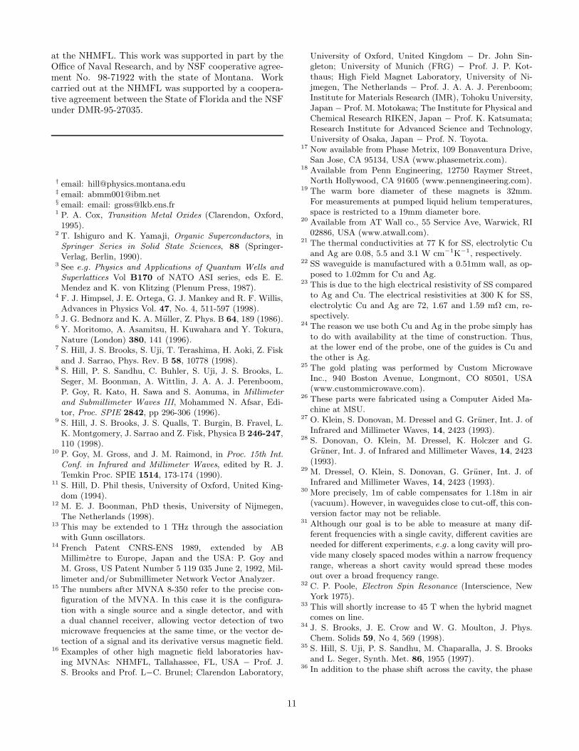
Fig. 10 shows a frequency sweep across the TE011mode of an axial cavity (cavity A, height = 6.7mm, dia.= 9.52mm, see Table II); the cavity is loaded with asample of κ-(BEDT-TTF)2Cu(SCN)2 (approx. dimen-sions 0.5× 0.50× 0.2 mm3)35 in the end plate configura-tion, and the temperature is 4.2 K. In the upper panel,we plot linear amplitude versus phase. The data points(squares) form a perfect circle passing through the origin,indicating negligible leak vector. The frequency intervalbetween each point is approximately 250 kHz and thesolid line is a fit to the data. In the lower panel, we plotboth phase and linear amplitude (normalized) versus fre-quency. This resonance is perfectly symmetric due to thefact that the leak amplitude is 34.5 dB below the ampli-tude on resonance. The loaded Q−value of the cavity is
8
19,000 and, thus, the resonance width (2.34 MHz) is con-siderably less than the standing wave period, which is onthe order of 100 MHz. The absolute value of the phasereturned by the VR is arbitrary,36 which is why the phaseon resonance is 64o rather than 0o (see Fig. 4a). In anysubsequent experiment, we would null the phase on reso-nance, and interpret changes in the complex parametersof the signal returned to the VR according to the proce-dure described in section II-B.2. It should be noted thatthis data is about as good as one could expect were thecavity mounted on the bench top and the HG and HMconnected directly to the cavity, i.e. the influence of theintervening waveguides has been completely eliminated.
Next, we consider the influence of the nearby TM111mode on measurements made at the TE011 resonancefrequency. Fig. 11 shows two such resonances obtainedat liquid helium temperature (cavity A): the main partof the figure plots linear amplitude versus frequency; theinset shows the circles in the complex plane obtainedfor each of the resonances. The TM111 mode has beenshifted 230 MHz below the TE011 mode, which corre-sponds to almost 100 times the width of the TE011 mode(ΓTE011 = 2.42 MHz) and about 40 times the width of theTM111 mode (ΓTM111 = 5.73 MHz). The resonance am-plitude of the TM111 mode is about 60% of the TE011resonance amplitude. However, more importantly, thepower of the TM111 signal (Obtained by extrapolation ofa Lorentzian fit) is 44.5 dB below the power of the TE011signal when the TE011 mode is at resonance. Thus, forall intents and purposes, we can rule out any interferencebetween these modes. Even if there were a slight mixing,both modes have H-fields perpendicular to the appliedDC field (Bo) for the end-plate configuration, and the
TM111 mode has an H-field node at the center of thecavity where the sample is usually placed in the quartz-pillar configuration; this has been verified experimentallyusing electron paramagnetic resonance standards.37
Q−values as high as 24,900 have been obtained at liq-uid helium temperatures for the loaded axial cavities ex-cited in TE011 modes. In general, higher n (higher fo)TE01n modes have reduced Q−values. In addition, theshorter wavelengths associated with the higher frequen-cies slightly increases the leak amplitude relative to thesignal transmitted through the cavity. These facts, to-gether with the diminished dynamic range of the spec-trometer (see Table I) at higher frequencies, make itharder to observe TE01n (n > 1) resonances of compara-ble quality to the TE011 modes. Nevertheless, the datain Fig. 10 far exceeds the criteria discussed in sectionII-B for making successful cavity perturbation measure-ments. Consequently, we have been able to make reliablemeasurements at frequencies up to 130 GHz.
Above about 130 GHz, we have less confidence in themode assignment of the resonances. However, by follow-ing the frequency dependence of data containing distinctfeatures which also depend strongly on the polarizationof the AC-fields within the cavity (see following section),
we have been able to characterize and use axial cavitymodes all the way up to 180 GHz. Fig. 12 shows severalhigher n TE01n axial cavity modes, together with selec-tive higher frequency resonances. Table II lists the fre-quencies, Q−values, leak amplitudes and dynamic rangesassociated with these modes, as well as some parame-ters for the transverse cavity (all at 4.2 K). These figuresclearly demonstrate the potential of the system for cav-ity perturbation measurements. It should also be notedfrom Fig. 12 that many of the resonances were obtainedusing a single resonator (cavity A), which was one of themain objectives for this system from the very outset.31
In the following section, we show real data obtained overthe frequency range covered by this single cavity.
Finally, Fig. 13 illustrates the importance of usingactive temperature stabilization: the upper panel showsmagnetic resonance data taken at the base temperatureof the cryostat ( 1.4 K); the upper panel shows the samedata obtained using active temperature stabilization at1.8 K. A clear drift in the unlocked temperature data isobserved throughout the course the up and down sweepsof the magnetic field.
B. Experimental examples
By eliminating the influence of all components of thesample probe (aside from the cavity) on the signal re-turned to the VR, it is possible to record changes in thecomplex cavity parameters in real time, i.e. the vec-tor (either amplitude and phase, or amplitude and fre-quency) recorded at the VR is directly related to theimpedance of the cavity, ZC. Here, once again, we seethe power of the MVNA. Using a scalar detection scheme,it would be necessary to modulate the frequency in orderto extract the complex cavity response.28 This would in-evitably result in a much longer time for recording eachdata point. The MVNA essentially returns phase andamplitude information at the detection frequency of theVR, which is approximately 10 kHz.10,38 This aspect ofthe instrument described in this paper makes it highlysuited to measurements in high magnetic fields, whichcan be expensive to run for long periods.
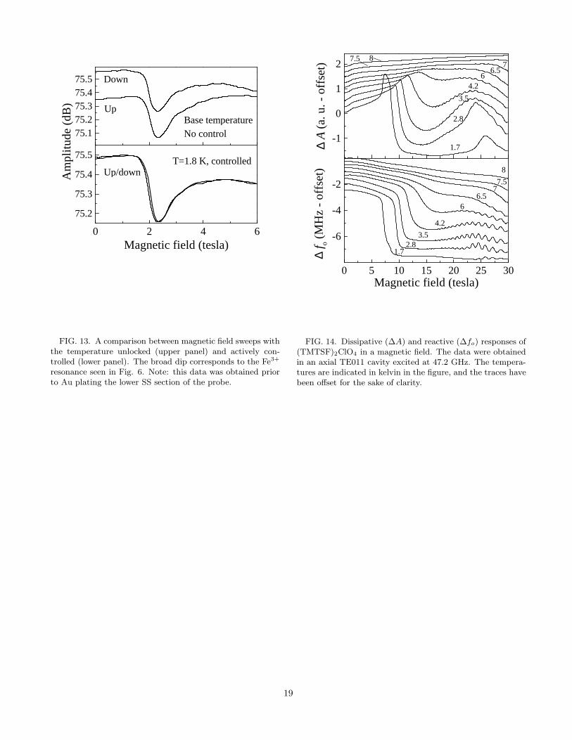
A distinct advantage of conducting fixed frequency op-tical measurements, as a function of magnetic field, isthat the spectral features which are under investigationmay be expected to change with field, i.e. the magneticfield is the variable which is used to tune the electronicexcitation spectrum of the material under investigation.If, for example, this induces a change from an insulat-ing state, to a metallic state, then the optical responseat frequencies comparable to the gap will reflect thischange. A beautiful example of this can be seen fromdata obtained at the NHMFL, (Fig. 14) which shows thecomplex electrodynamic response of the organic super-conductor (TMTSF)2ClO4, at low temperatures, as themagnetic field is swept to 30 tesla.39 A rich behavior isobserved; each of the more pronounced features may beattributed to modifications in the electronic configurationof the system which are known to occur in the field ranges
9

from 5 to 10 tesla (Field-Induced-Spin-Density-Waves -FISDW), and from 20 to 30 tesla (a phase line within thefinal FISDW phase).40 Magneto-quantum-oscillations arealso observed at high fields.
The data displayed in Fig. 14 were obtained using aphase lock while recording changes in amplitude (A) andthe resonance frequency (fo) of an axial cavity excitedat 47.2 GHz. The sample was oriented with its c* axisparallel to the applied DC magnetic field, Bo, and cur-rents were excited in the ab plane of the sample. Eachfield sweep took less than 10 minutes. The quality of thisdata is, at worst, comparable to an equivalent DC mea-surement. From the combined information obtained fromchanges in dissipation (∆A) and dispersion (∆fo) withinthe cavity, we can obtain valuable information about theelectrodynamics of the bound and free carrier systems inthis fascinating material.39,40
The above example is quite different from a zero-fieldmeasurement where data are usually taken at many fre-quencies in order to investigate a particular spectral fea-ture. Such experiments are generally plagued by poor dy-namic range (signal-to-noise), especially in the millime-ter and sub-millimeter spectral ranges. This is becauseidentical coupling between the sample and the spectrom-eter cannot be guaranteed at each frequency, resultingin a large scatter of the data. This is unfortunate, sincethe cavity perturbation technique is inherently sensitiveand, through the use of a suitable spectrometer (e.g. theMVNA), provides plenty of dynamic range at any givenfrequency. The instrument described in this paper is,instead, optimized at each frequency in order to detectminute changes in the optical conductivity of a sample asa function of magnetic field. These changes may subse-quently be normalized to the zero-field conductivity usingan appropriate instrument.
Whether to choose a phase lock or a frequency lockdepends on the experiment. A frequency lock generallyprovides better stability because of the higher Q−value ofthe quartz frequency reference, as compared to the cav-ity. Fig. 15 shows an example of separate measurementsusing both techniques. The sample under investigationis the purple bronze η−Mo4O11.
9,41 Fig. 15a shows vari-ations in amplitude for both up and down sweeps of themagnetic field. There is a slight hysteresis, which is welldocumented for this material. However, the transmittedamplitude is considerably lower at high magnetic fieldsfor the frequency locked measurement. This can be at-tributed to the cavity going well off resonance, as evi-denced by a phase change of 25o in the first 7 or 8 tesla(Fig 15b). Inspection of Fig. 4 clearly illustrates that a25o phase shift will lead to such a reduction in amplitude,even if there is no change in the dissipation within thecavity. Indeed, the ratio of the amplitudes obtained byeach technique scales nicely with the cosine of the phaseshift, as shown in the inset to Fig. 15b. Consequently,the frequency lock is inappropriate in this case, becauseof considerable mixing of the dissipative and dispersiveresponses of the sample in the phase and amplitude re-
turned to the VR. Fig. 15c shows the frequency shiftobserved using the phase lock.
Fig. 16 shows Periodic Orbit Resonances (PORs− related to cyclotron resonance)42 observed throughthe inter-layer conductivity of the quasi-two-dimensionalorganic conductor α−(BEDT-TTF)2TlHg(NCS)4.
43,44
The frequencies, which are indicated above each trace inthe figure, were obtained using a single axial cavity, andrange all the way from 44 GHz to 182 GHz. The samplewas mounted in the end-plate configuration. Not all ofthe frequencies correspond to TE01n modes. However,from the shapes of the resonances (∼Lorentzian peaks),we can be certain that the sample sits in the same electro-magnetic environment for all of the modes, i.e. with thepolarization of the oscillatory H-field parallel to the con-ducting layers, resulting in the excitation of inter-layercurrents (see Fig. 9d). This can be confirmed by study-ing the same sample in the TE011 quartz pillar config-uration, as shown in Fig. 17, which is the conventionalgeometry for observing cyclotron resonance. Because ofa high in-plane conductivity, it is the in-plane surface re-sistance of the sample that governs the dissipation in thecavity (see Fig. 9c).27,45 This is the reason for the ratherunconventional lineshape, i.e. an inflection rather thana symmetric dip or peak.
The data in Figs 16 and 17 are exceptional in theirquality when compared to earlier attempts to measure cy-clotron resonance in organic conductors.46 Furthermore,the resonance line shapes agree precisely with theory,thereby providing absolute confidence in the ability ofthe technique to discriminate between in-plane and inter-layer transport phenomena in quasi-two-dimensional con-ductors. This has traditionally been problematic usingconventional DC resistivity probes, because of uncertain-ties in the current paths within the samples. This opensup a huge range of possibilities for tackling issues con-cerning the role of electronic dimensionality in the phys-ical properties of low-dimensional systems.
IV. SUMMARY
We have described an instrument for conductingmillimeter-wave cavity perturbation measurements overa continuously tunable frequency range (40 − 200 GHz).The system is compatible with magnets both at Mon-tana State University (up to 9 tesla) and at the NationalHigh Magnetic Field Laboratory (up to 33 tesla) in Tal-lahassee, FL. The utilization of a Millimeter-wave VectorNetwork Analyzer enables simultaneous measurements ofthe complex cavity parameters (resonance frequency andQ−value) at a rapid repetition rate (∼ 10 kHz). Severalexperimental examples are presented which demonstratethe potential of this system for studying the magneto-electrodynamics of low-dimensional conducting systems.
ACKNOWLEDGEMENTS
We are indebted to Norm Williams for technical assis-tance and to Prof. J. S. Brooks for the use of the MVNA
10
at the NHMFL. This work was supported in part by theOffice of Naval Research, and by NSF cooperative agree-ment No. 98-71922 with the state of Montana. Workcarried out at the NHMFL was supported by a coopera-tive agreement between the State of Florida and the NSFunder DMR-95-27035.
† email: [email protected]‡ email: [email protected]§ email: email: [email protected] P. A. Cox, Transition Metal Oxides (Clarendon, Oxford,1995).
2 T. Ishiguro and K. Yamaji, Organic Superconductors, inSpringer Series in Solid State Sciences, 88 (Springer-Verlag, Berlin, 1990).
3 See e.g. Physics and Applications of Quantum Wells and
Superlattices Vol B170 of NATO ASI series, eds E. E.Mendez and K. von Klitzing (Plenum Press, 1987).
4 F. J. Himpsel, J. E. Ortega, G. J. Mankey and R. F. Willis,Advances in Physics Vol. 47, No. 4, 511-597 (1998).
5 J. G. Bednorz and K. A. Muller, Z. Phys. B 64, 189 (1986).6 Y. Moritomo, A. Asamitsu, H. Kuwahara and Y. Tokura,Nature (London) 380, 141 (1996).
7 S. Hill, J. S. Brooks, S. Uji, T. Terashima, H. Aoki, Z. Fiskand J. Sarrao, Phys. Rev. B 58, 10778 (1998).
8 S. Hill, P. S. Sandhu, C. Buhler, S. Uji, J. S. Brooks, L.Seger, M. Boonman, A. Wittlin, J. A. A. J. Perenboom,P. Goy, R. Kato, H. Sawa and S. Aonuma, in Millimeter
and Submillimeter Waves III, Mohammed N. Afsar, Edi-tor, Proc. SPIE 2842, pp 296-306 (1996).
9 S. Hill, J. S. Brooks, J. S. Qualls, T. Burgin, B. Fravel, L.K. Montgomery, J. Sarrao and Z. Fisk, Physica B 246-247,110 (1998).
10 P. Goy, M. Gross, and J. M. Raimond, in Proc. 15th Int.
Conf. in Infrared and Millimeter Waves, edited by R. J.Temkin Proc. SPIE 1514, 173-174 (1990).
11 S. Hill, D. Phil thesis, University of Oxford, United King-dom (1994).
12 M. E. J. Boonman, PhD thesis, University of Nijmegen,The Netherlands (1998).
13 This may be extended to 1 THz through the associationwith Gunn oscillators.
14 French Patent CNRS-ENS 1989, extended by ABMillimetre to Europe, Japan and the USA: P. Goy andM. Gross, US Patent Number 5 119 035 June 2, 1992, Mil-limeter and/or Submillimeter Network Vector Analyzer.
15 The numbers after MVNA 8-350 refer to the precise con-figuration of the MVNA. In this case it is the configura-tion with a single source and a single detector, and witha dual channel receiver, allowing vector detection of twomicrowave frequencies at the same time, or the vector de-tection of a signal and its derivative versus magnetic field.
16 Examples of other high magnetic field laboratories hav-ing MVNAs: NHMFL, Tallahassee, FL, USA − Prof. J.S. Brooks and Prof. L−C. Brunel; Clarendon Laboratory,
University of Oxford, United Kingdom − Dr. John Sin-gleton; University of Munich (FRG) − Prof. J. P. Kot-thaus; High Field Magnet Laboratory, University of Ni-jmegen, The Netherlands − Prof. J. A. A. J. Perenboom;Institute for Materials Research (IMR), Tohoku University,Japan − Prof. M. Motokawa; The Institute for Physical andChemical Research RIKEN, Japan − Prof. K. Katsumata;Research Institute for Advanced Science and Technology,University of Osaka, Japan − Prof. N. Toyota.
17 Now available from Phase Metrix, 109 Bonaventura Drive,San Jose, CA 95134, USA (www.phasemetrix.com).
18 Available from Penn Engineering, 12750 Raymer Street,North Hollywood, CA 91605 (www.pennengineering.com).
19 The warm bore diameter of these magnets is 32mm.For measurements at pumped liquid helium temperatures,space is restricted to a 19mm diameter bore.
20 Available from AT Wall co., 55 Service Ave, Warwick, RI02886, USA (www.atwall.com).
21 The thermal conductivities at 77 K for SS, electrolytic Cuand Ag are 0.08, 5.5 and 3.1 W cm−1K−1, respectively.
22 SS waveguide is manufactured with a 0.51mm wall, as op-posed to 1.02mm for Cu and Ag.
23 This is due to the high electrical resistivity of SS comparedto Ag and Cu. The electrical resistivities at 300 K for SS,electrolytic Cu and Ag are 72, 1.67 and 1.59 mΩ cm, re-spectively.
24 The reason we use both Cu and Ag in the probe simply hasto do with availability at the time of construction. Thus,at the lower end of the probe, one of the guides is Cu andthe other is Ag.
25 The gold plating was performed by Custom MicrowaveInc., 940 Boston Avenue, Longmont, CO 80501, USA(www.custommicrowave.com).
26 These parts were fabricated using a Computer Aided Ma-chine at MSU.
27 O. Klein, S. Donovan, M. Dressel and G. Gruner, Int. J. ofInfrared and Millimeter Waves, 14, 2423 (1993).
28 S. Donovan, O. Klein, M. Dressel, K. Holczer and G.Gruner, Int. J. of Infrared and Millimeter Waves, 14, 2423(1993).
29 M. Dressel, O. Klein, S. Donovan, G. Gruner, Int. J. ofInfrared and Millimeter Waves, 14, 2423 (1993).
30 More precisely, 1m of cable compensates for 1.18m in air(vacuum). However, in waveguides close to cut-off, this con-version factor may not be reliable.
31 Although our goal is to be able to measure at many dif-ferent frequencies with a single cavity, different cavities areneeded for different experiments, e.g. a long cavity will pro-vide many closely spaced modes within a narrow frequencyrange, whereas a short cavity would spread these modesout over a broad frequency range.
32 C. P. Poole, Electron Spin Resonance (Interscience, NewYork 1975).
33 This will shortly increase to 45 T when the hybrid magnetcomes on line.
34 J. S. Brooks, J. E. Crow and W. G. Moulton, J. Phys.Chem. Solids 59, No 4, 569 (1998).
35 S. Hill, S. Uji, P. S. Sandhu, M. Chaparalla, J. S. Brooksand L. Seger, Synth. Met. 86, 1955 (1997).
36 In addition to the phase shift across the cavity, the phase
11

returned to the VR includes an additional phase shift dueto the path difference between the signals reaching the HMfrom S1 and S2.
37 S. Hill et al., to be published elsewhere.38 Although the VR detects at 10 kHz, it is common to aver-
age this signal over about 50 cycles, resulting in a detectionfrequency of about 200 Hz.
39 S. Hill; J.S. Brooks; J.S. Qualls; B.W. Fravel; L.K. Mont-gomery, accepted for publication in Synth. Met. (1998).
40 S. K. McKernan, S. T. Hannahs, U. M. Scheven, G. M.Danner and P. M. Chaikin, Phys. Rev. Lett. 75, 1630(1995).
41 S. Hill, S. Valfells, S. Uji, J. S. Brooks, G. J. Athas, P.S. Sandhu, J. Sarrao, Z. Fisk, J. Goettee, H. Aoki and T.Terashima, Phys. Rev. B 55, 2018 (1997).
42 Stephen Hill, Phys. Rev. B 55, 4931 (1997).43 Stephen Hill, M. Mola, J. S. Brooks, M. Tokumoto, N. Ki-
noshita, T. Kinoshita and Y. Tanaka, to be published inProc. ”Physical Phenomena in High Magnetic Fields III”
(PPHMF-III), eds Z. Fisk, L. P. Gor’kov and J. R. Schri-
effer (World Scientific, Singapore 1999).44 S. Hill et al., in preparation.45 S. Hill, P. S. Sandhu, M. Boonman, J. A. A. J. Perenboom,
A. Wittlin, S. Uji, J. S. Brooks, R. Kato, H. Sawa and S.Aonuma, Phys. Rev. B 54, 13536 (1996).
46 See e.g: J. Singleton, F. L. Pratt, M. Doporto, T. J. B.M. Janssen, M. Kurmoo, J. A. A. J. Perenboom, W. Hayesand P. Day, Phys. Rev. Lett. 68, 2500 (1992); S. Hill, A.Wittlin, J. van-Bentum, J. Singleton, W. Hayes, J. A. A. J.Perenboom, M. Kurmoo and P. Day, Synth. Met. 70, 821(1995); S. V. Demishev, A. V. Semeno, N. E. Sluchanko, N.A. Samarin, I. B. Voskoboinikov, V. V. Glushkov, J. Single-ton, S. J. Blundell, S. O. Hill, W. Hayes, M. V. Kartsovnik,A. E. Kovalev, M. Kurmoo, P. Day and N. D. Kushch,Phys. Rev. B 53, 12794 (1996); A. Polisskii, J. Singleton,P. Goy, W. Hayes, M. Kurmoo and P. Day, J. Phys.: Cond.Mat. 8, L195 (1996); and A. Ardavan, J. M. Schrama, S.J. Blundell, J. Singleton, W. Hayes, M. Kurmoo, P. Dayand P. Goy, Phys. Rev. Lett. 81, 713 (1998).
12
Band,
harmonic
Frequency
(GHz)
Dynamic range -
analyzer (dB)
V, N=3 48 >128
V, N=4 60 >128
V, N=4 70 126.4
W, N=5 79 105.7
W, N=5 88 103
W, N=6 99 94
W, N=6 108 83.8
D, N=8 119 83
D, N=9 135 76.8
D, N=10 157 65.3
D, N=12 186 57.8
TABLE I. The dynamic ranges achieved using the MVNA-8-350 at MSU at various frequencies in each microwave band.
Band/harmonic Cavity/mode fo (GHz) Q S/N (dB) A(fo) - Al (dB)
V - 3 A1 - TE011 44.450 19,000 76.0 34.5
V - 3 A1 - TM111 44.219 7,700 74.6 19.0
V - 3 B1 - TE011 44.414 24,900 81.4 26.0
V - 3 B1 - TM111 44.265 7,400 80.3 13.8
V - 4 A1 - TE012 58.754 13,900 85.4 27.0
V - 4 A1 - TE212 53.951 10,400 87.8 40.4
V - 4 A1 - TE312 61.247 10,000 90.4 24.5
V - 4 A1 - TE412 68.906 4,800 92.4 20.8
W - 5 A2 - TE213 73.924 8,800 84.5 25.0
W - 5 A2 - TE013 78.044 7,900 89.0 23.0
W - 5 A2 88.678 23,000 90.0 22.0
W - 6 A2 - TE014 98.715 5,300 83.0 16.5
W - 6 A2 103.532 4,350 84.5 27.0
D - 8 C3 - TE014 127.233 13,600 45.8 16.5
D - 9 C3 145.227 7,900 48.5 17.5
D - 10 C3 155.815 5,800 41.2 21.0
D - 12 C3 187.686 5,150 31.0 4.0
V-4 T - TE012 56.110 15,500 81.9 18.0
V-4 T - TE013 65.078 14,000 74.6 13.0
TABLE II. Resonance parameters for different modes obtained in various different cavities. The first column lists thefrequency band and the MVNA harmonic. The second column lists the cavity (letter) and end plate used (number), as wellas the mode (if known); cavities A, B and C have dimensions (length × diameter) 6.7mm × 9.52mm, 8.73mm × 9mm, and5.54mm × 5.64mm respectively, cavity T is the transverse cavity (10.16mm × 7.75mm), and end plates 1, 2 and 3 havecoupling hole diameters of 1.32mm, 0.84mm and 0.62mm, respectively. The next three columns list the resonance frequencies(fo), Q−values and dynamic ranges (signal-to-noise) for each mode. The final column lists the contrast in dB between thetransmitted amplitude on resonance [A(fo)] and the leak amplitude (Al). The dynamic range is somewhat lower at 45 GHzthan in the main part of the V- and W-bands due to the fact that the V-band wave-guide is so close to cut off at these lowfrequencies.
13
Coax
Schottkydiodes
Vacuumtightwindows
Coax
Vacuum jacket
Radiationbaffles
LiquidNitrogen
LiquidHelium
Cavity
Waveguides
Innercryostat
Waveguidecouplers
Solenoid
Cu/Ag
SS
FIG. 1. Schematic of the sample probe and superconduct-ing magnet system at MSU (not to scale).
lc
cc
Transmissionwaveguide
ZT
mHG
mo u t
mHM
ml
min
ZC
ZI
rc
HG HM
Incidentwaveguide
FIG. 2. An equivalent LRC circuit representation of thekey microwave components of the sample probe. The cou-pling between HG (HM) and the incidence (transmission)waveguide is modeled as a coupling mutual inductance mHG
(mHM). The cavity is coupled to each of the waveguidesthrough coupling mutual input (min) and output (mout) in-ductances. A leak signal between the incidence and trans-mission waveguides, in parallel with the cavity, is modeledas a direct coupling mutual inductance, ml, between the twowaveguides.
52 54 56 58 60 62 64-16
-14
-12
-10
-8
-6
-4
-2
0
Stainless steel
Silver
Pow
er lo
ss (
dB/m
)
Frequency (GHz)
FIG. 3. A comparison between the insertion losses (indB/m) for stainless steel and Silver waveguide sections inV-band at room temperature.
14
0
30
6090
120
150
180
210
240270
300
330
0.0
0.5
1.0
59.95 60.00 60.05-0.5
0.0
0.5
1.0
1P
hase
fo
A2(f)
A1(f)c)
a)
Frequency (GHz)
-0.5
0.0
0.5
1.0
-50
0
50
100Phase
b)
Nor
mal
ized
am
plit
ude
FIG. 4. Simulation of the complex parameters of a wavetransmitted through a cavity which is resonant at 60 GHz,and has a Q of 5000; a) a plot of linear amplitude versusphase in the complex plane; b) a plot of linear amplitude(normalized) and phase versus frequency; and c) a plot of thereal (A1) and imaginary (A2) linear amplitudes (normalized)versus frequency.
0
30
6090
120
150
180
210
240270
300
330
0.0
0.5
1.0
59.95 60.00 60.050
90
180
270
360
1
Pha
se
fo
c)
a)
Pha
se
Frequency (GHz)
0.20.40.60.81.0
fo
b)Am
plit
ude
FIG. 5. A demonstration of the effect of a leak wave on theideal resonance in Fig. 4. The complex leak vector translatesthe resonance in the complex plane, as shown by the arrow ina). The result is that the resonance frequency, fo, no longerlies along the real axis (φ = 0). Thus, fo no longer corre-sponds to the maximum amplitude, resulting in the distortedLorentzian lineshape shown in b) and c).
15

0 1 2 3 4 5 6 7
-0.3
-0.2
-0.1
0.0
0.1
0.2
Au plated [CMI]25
Au plated (MSU) Unplated
Cha
nge
in A
mpl
itud
e (d
B -
off
set)
Magnetic field (tesla)
FIG. 6. A comparison between the background (empty Cucavity) response of the sample probe using Gold plated andunplated stainless steel sections at the lower end of the probe;these data were obtained at 76.7 GHz and 4.2 K. The broaddip is attributed to an EPR absorption due to small quantitiesof Fe3+ (rust) at the surface of the SS. Professional gold plat-ing (solid line) clearly eliminates this contamination, which isevident both in the unplated data (short dash) and the dataobtained after our efforts to plate the SS at MSU (long dash).
FIG. 7. Schematic of the axial cavity construction. Seetext for detailed description.
16

FIG. 8. Schematic of the transverse cavity construction.See text for detailed description. Bo
H
e)
H
d)
Hc)
a) b)
FIG. 9. a) The end plate cavity perturbation configuration,showing the position of the sample within a TE011 cavityand the radial H-field at the position of the sample. b) Thequartz pillar configuration, showing the sample at the heart ofa TE011 cavity atop a quartz pillar, and the axial H-field atthe position of the sample. c) Excitation of in-plane currentsat the edges of a Q2D conductor. d) Excitation of inter-layercurrents within the bulk of a Q2D conductor. In both c) andd), the low conductivity direction is parallel to the normal tothe disc shaped sample. e) Sample rotation for the quartzpillar configuration in the transverse cavity − note that theorientation of the axial AC H-field does not change relativeto the sample upon rotation.
17
0
30
6090
120
150
180
0.2
0.4
0.6
0.8
Phase
44.440 44.445 44.450 44.455
0.0
0.3
0.6
0.9
1.2
0
30
60
90
120
Nor
mal
ized
am
plit
ude
Phase (degrees)
Frequency (GHz)
FIG. 10. A real TE011 resonance (raw data at 4.2 K) for aloaded axial cavity (cavity A). The upper panel shows the res-onance circle in the complex plane - the squares are raw dataand the solid line is a fit. The lower panel shows the linearamplitude and phase variation as a function of frequency.
0
30
6090
120
150
180
210
240270
300
330
0.0
0.2
0.4
0.6
0.8
1.0
44.2 44.3 44.40.0
0.2
0.4
0.6
0.8
1.0Phase TE011
TM111
Nor
mal
ized
am
plit
ude
Frequency (GHz)
FIG. 11. Lifting the degeneracy of the TE011 and TM111modes (T = 4.2 K) in cavity A. The main part of the fig-ure shows the two resonances (linear scale) separated by 230MHz. The inset shows the circles in the complex plane corre-sponding to the two resonances.
0
1000
2000
3000
4000
5000
6000
0
30
6090
120
150
180
210
240270
300
330
0
1000
2000
3000
4000
5000
6000
a)
180
54.0 GHz 58.8 GHz 61.2 GHz
0
500
1000
1500
0
30
6090
120
150
180
210
240270
300
330
0
500
1000
1500
b)
180
103.5 GHz 78.0 GHz 88.7 GHz
0
200
400
600
0
30
6090
120
150
180
210
240270
300
330
0
200
400
600
c)
126.9 GHz 155.9 GHz 169.1 GHz
180
FIG. 12. Various cavity resonances seen as circles in thecomplex plane, obtained in a) V-band, b) W-band and c)D-band. The points are raw 4.2 K data and the solid linesrepresent Lorentzian fits to the data. See table 2 for moredetails about each of the resonances.
18
0 2 4 6
75.2
75.3
75.4
75.5
Up/downT=1.8 K, controlled
Am
plit
ude
(dB
)
Magnetic field (tesla)
75.175.275.375.475.5 Down
UpBase temperatureNo control
FIG. 13. A comparison between magnetic field sweeps withthe temperature unlocked (upper panel) and actively con-trolled (lower panel). The broad dip corresponds to the Fe3+
resonance seen in Fig. 6. Note: this data was obtained priorto Au plating the lower SS section of the probe.
-1
0
1
287.5
76.5
64.2
3.5
2.8
1.7∆ A
(a.
u. -
off
set)
0 5 10 15 20 25 30
-6
-4
-2
Magnetic field (tesla)
8
7.57
6.56
4.2
3.52.8
1.7∆ f o (
MH
z -
offs
et)
FIG. 14. Dissipative (∆A) and reactive (∆fo) responses of(TMTSF)2ClO4 in a magnetic field. The data were obtainedin an axial TE011 cavity excited at 47.2 GHz. The tempera-tures are indicated in kelvin in the figure, and the traces havebeen offset for the sake of clarity.
19

0.7
0.8
0.9
1.0
a) Phase lock Frequency lockA
mpl
itud
e
135140145150155160
b) Frequency lockPha
se (
degr
ees)
0 5 10 15 20 25 30
-1.0-0.8-0.6-0.4-0.20.0
c)
Phase lock
∆ fo (
MH
z)
Magnetic field (tesla)
0 5 10 15 20 25 30
0.90
0.95
1.00 cos(∆φ)
ratio
FIG. 15. a) A comparison between the amplitude vari-ation versus magnetic field obtained using frequency andphase locking techniques. The sample is the purple bronzeη−Mo4O11, and the observed changes are due to the excita-tion of inter-layer currents in this quasi-two-dimensional con-ductor. b) Shows the phase variation during the frequencylocked measurement (absolute microwave frequency fixed at44.272 GHz), while c) shows the frequency variation dur-ing the phase locked measurement (absolute microwave phaseacross the sample probe locked). The inset to b) comparesthe ratio of the amplitudes obtained for the two techniques ina), with the cosine of the phase change in the main part of b).The good correspondence between these quantities confirmsthat the difference between the traces in a) can be attributedto the large phase shift during the frequency locked measure-ment. Thus, a phase lock should be applied in this situation.
0 1 2 3 4 5 6 7-400
-300
-200
-100
0
100
200
300
400
182
162
146123
116
90
83
7664
44
∆σzz (
arb.
uni
ts -
off
set)
Magnetic field (tesla)
FIG. 16. Frequency dependence of the Periodic Orbit Res-onances observed through the inter-layer conductivity (σzz)in α−(BEDT-TTF)2TlHg(NCS)4, when mounted in a TE011axial cavity in the end plate configuration; the temperatureis 1.8 K. The data appear noisier at higher frequencies dueto the reduced dynamic range of the spectrometer and dueto the reduced sensitivity (lower Q−values) of the higher or-der cavity modes. The resonances have been scaled so as toappear the same strength, and have been offset for the sakeof clarity. The sharp spikes observed slightly above the mainpeak positions are Electron Paramagnetic Resonance signalsdue to a DPPH sample placed in the cavity.
0 1 2 3 4 5 63.0
3.5
4.0
4.5
5.0
Cyclotronresonance
ν = 44.27 GHz
Currents in-plane
2 K 3 K 4 K 5 K 6 K 7 K
Sur
face
res
ista
nce
(arb
. uni
ts)
Magnetic field (tesla)
FIG. 17. Conventional cyclotron resonances seen throughthe in-plane surface resistance for the same sample as in Fig.16, this time mounted in a TE011 axial cavity in the quartzpillar configuration; the frequency is 44.27 GHz and the tem-peratures are indicated in the figure. The resonances are ob-served as sharp inflections which weaken as the temperatureincreases.
20
Copyright © 2022 FDOKUMEN