Influence of single and double deposition temperatures on the interface quality of atomic layer...
8
Influence of single and double deposition temperatures on the interface quality of atomic layer deposited Al 2 O 3 dielectric thin films on silicon S. Dueñas, a H. Castán, H. García, A. de Castro, and L. Bailón Departamento de Electricidad y Electrónica, ETSI Telecomunicación, Universidad de Valladolid, Campus “Miguel Delibes,” 47011 Valladolid, Spain K. Kukli b Institute of Experimental Physics and Technology, University of Tartu, Tähe 4, 51010 Tartu, Estonia A. Aidla, J. Aarik, H. Mändar, and T. Uustare Institute of Physics, University of Tartu, Riia 142, 51014 Tartu, Estonia J. Lu Ångström Microstructure Laboratory, Department of Engineering Sciences, Uppsala University, P.O. Box 534, SE-751 21 Uppsala, Sweden A. Hårsta The Ångström Laboratory, Department of Materials Chemistry, Uppsala University, P.O. Box 538, SE-751 21 Uppsala, Sweden Received 31 May 2005; accepted 19 January 2006; published online 3 March 2006 An electrical characterization of Al 2 O 3 based metal-insulator-semiconductor structures has been carried out by using capacitance-voltage, deep level transient spectroscopy, and conductance-transient G-t techniques. Dielectric films were atomic layer deposited ALD at temperatures ranging from 300 to 800 °C directly on silicon substrates and on an Al 2 O 3 buffer layer that was grown in the same process by using 15 ALD cycles at 300 °C. As for single growth temperatures, 300 °C leads to the lowest density of states distributed away from the interface to the insulator disorder-induced gap states DIGS, but to the highest interfacial state density D it . However, by using 300/ 500 ° C double growth temperatures it is possible to maintain low DIGS values and to improve the interface quality in terms of D it . The very first ALD cycles define the dielectric properties very near to the dielectric-semiconductor interface, and growing an upper layer at higher ALD temperature produces some annealing of interfacial states, thus improving the interface quality. Also, samples in which the only layer or the upper one was grown at the highest temperature 800 °C show the poorest results both in terms of D it and DIGS, so using very high temperatures yield defective dielectric films. © 2006 American Institute of Physics. DOI: 10.1063/1.2177383 I. INTRODUCTION A key element in the fabrication of smaller and faster transistors for future ultralarge scale integrated circuits is the development of alternative materials, labeled high-k dielec- trics, which can replace silicon dioxide as the gate dielectric. So, a gate over a thick material having a larger dielectric constant can control the channel just as effectively as one over thinner lower-k dielectric. The thicker the dielectric layer, the less current is leaked between the gate and the substrate. The identification of alternative high-k gate dielec- tric materials system to replace SiO 2 requires the consider- ation of fundamental properties permittivity, barrier height, stability in direct contact with silicon, and film morphology and device processing and integration, as well as perfor- mance issues interface quality, gate compatibility, process compatibility, and reliability. Any successful gate dielectric solution requires both of these categories to be addressed simultaneously. While the materials properties can be used as initial selection criteria for suitable high-k dielectric candi- date, device issues can be used for further evaluation. In order to limit the leakage current, barrier height must also be considered together with permittivity of the high-k gate dielectrics. Indeed, the barrier height for electrons trav- eling from the silicon substrate to the gate is the conduction band offset E C . For electron direct tunneling transport, leakage current increases exponentially with decreasing bar- rier height, so it is desirable to find a gate dielectric that has a large E C value to silicon. However, many of the metal oxide and complex oxide materials, such as Ta 2 O 5 and SrTiO 3 , have E C 0.5 eV on Si. 1 If we assume reasonable symmetry of the band edges, a large band gap would corre- spond to a large conduction band offset. However, care must be taken because the band structure for some materials also has a large valence band offset E V , which consumes most of the band gap. So, metal oxides with high band gap such as Al 2 O 3 have been widely considered as possible candidates to a FAX: 34983423675; electronic mail: [email protected] b Also at Department of Chemistry, University of Helsinki, P.O. Box 55, FIN-00014 University of Helsinki, Finland JOURNAL OF APPLIED PHYSICS 99, 054902 2006 0021-8979/2006/995/054902/8/$23.00 © 2006 American Institute of Physics 99, 054902-1 Downloaded 06 Mar 2006 to 157.88.111.70. Redistribution subject to AIP license or copyright, see http://jap.aip.org/jap/copyright.jsp
-
Upload
independent -
Category
Documents
-
view
5 -
download
0
Transcript of Influence of single and double deposition temperatures on the interface quality of atomic layer...

JOURNAL OF APPLIED PHYSICS 99, 054902 �2006�
Influence of single and double deposition temperatures on the interfacequality of atomic layer deposited Al2O3 dielectric thin filmson silicon
S. Dueñas,a� H. Castán, H. García, A. de Castro, and L. BailónDepartamento de Electricidad y Electrónica, ETSI Telecomunicación, Universidad de Valladolid,Campus “Miguel Delibes,” 47011 Valladolid, Spain
K. Kuklib�
Institute of Experimental Physics and Technology, University of Tartu, Tähe 4, 51010 Tartu, Estonia
A. Aidla, J. Aarik, H. Mändar, and T. UustareInstitute of Physics, University of Tartu, Riia 142, 51014 Tartu, Estonia
J. LuÅngström Microstructure Laboratory, Department of Engineering Sciences, Uppsala University,P.O. Box 534, SE-751 21 Uppsala, Sweden
A. HårstaThe Ångström Laboratory, Department of Materials Chemistry, Uppsala University, P.O. Box 538,SE-751 21 Uppsala, Sweden
�Received 31 May 2005; accepted 19 January 2006; published online 3 March 2006�
An electrical characterization of Al2O3 based metal-insulator-semiconductor structures has beencarried out by using capacitance-voltage, deep level transient spectroscopy, andconductance-transient �G-t� techniques. Dielectric films were atomic layer deposited �ALD� attemperatures ranging from 300 to 800 °C directly on silicon substrates and on an Al2O3 buffer layerthat was grown in the same process by using 15 ALD cycles at 300 °C. As for single growthtemperatures, 300 °C leads to the lowest density of states distributed away from the interface to theinsulator �disorder-induced gap states �DIGS��, but to the highest interfacial state density �Dit�.However, by using 300/500 °C double growth temperatures it is possible to maintain low DIGSvalues and to improve the interface quality in terms of Dit. The very first ALD cycles define thedielectric properties very near to the dielectric-semiconductor interface, and growing an upper layerat higher ALD temperature produces some annealing of interfacial states, thus improving theinterface quality. Also, samples in which the only layer or the upper one was grown at the highesttemperature �800 °C� show the poorest results both in terms of Dit and DIGS, so using very hightemperatures yield defective dielectric films. © 2006 American Institute of Physics.�DOI: 10.1063/1.2177383�
I. INTRODUCTION
A key element in the fabrication of smaller and fastertransistors for future ultralarge scale integrated circuits is thedevelopment of alternative materials, labeled high-k dielec-trics, which can replace silicon dioxide as the gate dielectric.So, a gate over a thick material having a larger dielectricconstant can control the channel just as effectively as oneover thinner lower-k dielectric. The thicker the dielectriclayer, the less current is leaked between the gate and thesubstrate. The identification of alternative high-k gate dielec-tric materials system to replace SiO2 requires the consider-ation of fundamental properties �permittivity, barrier height,stability in direct contact with silicon, and film morphology�and device processing and integration, as well as perfor-mance issues �interface quality, gate compatibility, processcompatibility, and reliability�. Any successful gate dielectric
a�FAX: �34983423675; electronic mail: [email protected]�Also at Department of Chemistry, University of Helsinki, P.O. Box 55,
FIN-00014 University of Helsinki, Finland
0021-8979/2006/99�5�/054902/8/$23.00 99, 05490
Downloaded 06 Mar 2006 to 157.88.111.70. Redistribution subject to
solution requires both of these categories to be addressedsimultaneously. While the materials properties can be used asinitial selection criteria for suitable high-k dielectric candi-date, device issues can be used for further evaluation.
In order to limit the leakage current, barrier height mustalso be considered together with permittivity of the high-kgate dielectrics. Indeed, the barrier height for electrons trav-eling from the silicon substrate to the gate is the conductionband offset �EC. For electron direct tunneling transport,leakage current increases exponentially with decreasing bar-rier height, so it is desirable to find a gate dielectric that hasa large �EC value to silicon. However, many of the metaloxide and complex oxide materials, such as Ta2O5 andSrTiO3, have �EC�0.5 eV on Si.1 If we assume reasonablesymmetry of the band edges, a large band gap would corre-spond to a large conduction band offset. However, care mustbe taken because the band structure for some materials alsohas a large valence band offset �EV, which consumes mostof the band gap. So, metal oxides with high band gap such as
Al2O3 have been widely considered as possible candidates to© 2006 American Institute of Physics2-1
AIP license or copyright, see http://jap.aip.org/jap/copyright.jsp
054902-2 Dueñas et al. J. Appl. Phys. 99, 054902 �2006�
replace silicon dioxide.2,3 Indeed, Al2O3 exhibits the largestband gap �8.8 eV� next to SiO2 with a conduction band offsetof 2.8 eV with respect to silicon, 4.9 eV valence band offset,and thermodynamic stability against Si. Moreover, Al2O3 isknown to act as an oxygen diffusion barrier and also as agood glass former. However, it has relatively low k �8–10� incomparison to other candidates such as TiO2, with k�50 buthigh leakage current.
Besides these fundamental material issues, the deposi-tion process of the high-k gate dielectrics is also a crucialfactor in determining the final film quality and properties.The deposition technique of the choice must be compatiblewith current or expected complementary metal oxide semi-conductor �CMOS� process flow, and also it must offer goodconformality and thickness control, high wafer throughputs,and compatibility with emerging wafer processing guide-lines. Also, some process-induced issues such as residual im-purities from precursors and damage induced by reactive andenergetic particles must be minimized. Atomic layer deposi-tion �ALD� is very suitable for obtaining uniform thicknessfilms.4,5 Indeed, ALD is a stepwise film growth process onmonolayer scale that exploits the binding energy differencebetween chemisorption and physisorption at the substratesurface. In this process one reactant at a time is injected intothe growth area, and following surface reaction, excess spe-cies and by-products are purged with an inert gas. As a re-sult, films are grown by sequential surface reactions. Thismethod enables precise control of film composition andthickness as the growth proceeds one monolayer at a time onan atomic scale. One of the major difficulties to high-k di-electric integration into silicon technology is the presence ofelectrically active defects in this kind of materials. Thesedefects can play an important role in the final device opera-tion. However, so far very little is known about the nature ofdefects or about possible techniques to eliminate them. So, agreat effort must be developed in order to increase the gen-eral knowledge in this field before high-k materials will beready for high volume production in the gate stack.
As a contribution to this subject, this work presents anelectrical characterization of metal-insulator-semiconductor�MIS� structures fabricated by atomic layer depositing Al2O3
thin films on silicon substrates by using AlCl3 and H2O asprecursors. Basically all the ALD Al2O3 studies on gate ox-
6
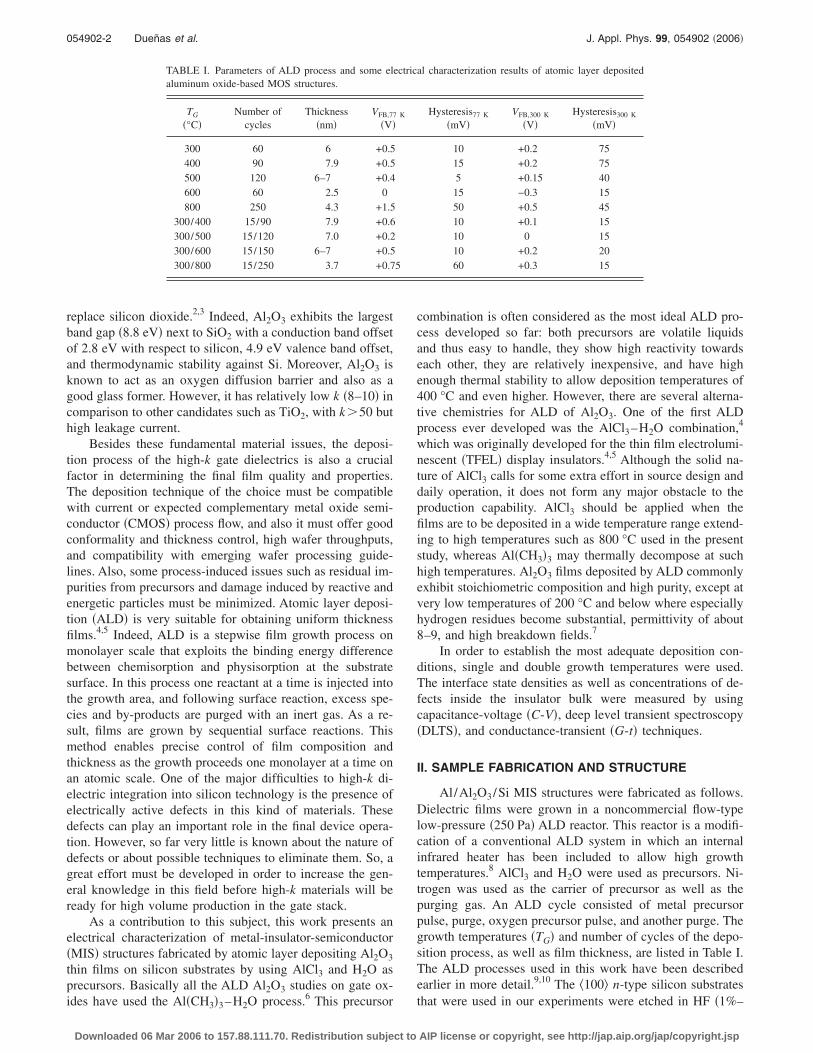
TABLE I. Parameters of ALD process and some elealuminum oxide-based MOS structures.
TG
�°C�Number of
cyclesThickness
�nm�VFB,77
�V�
300 60 6 +0.5400 90 7.9 +0.5500 120 6–7 +0.4600 60 2.5 0800 250 4.3 +1.5
300/400 15/90 7.9 +0.6300/500 15/120 7.0 +0.2300/600 15/150 6–7 +0.5300/800 15/250 3.7 +0.7
ides have used the Al�CH3�3–H2O process. This precursor
Downloaded 06 Mar 2006 to 157.88.111.70. Redistribution subject to
combination is often considered as the most ideal ALD pro-cess developed so far: both precursors are volatile liquidsand thus easy to handle, they show high reactivity towardseach other, they are relatively inexpensive, and have highenough thermal stability to allow deposition temperatures of400 °C and even higher. However, there are several alterna-tive chemistries for ALD of Al2O3. One of the first ALDprocess ever developed was the AlCl3–H2O combination,4
which was originally developed for the thin film electrolumi-nescent �TFEL� display insulators.4,5 Although the solid na-ture of AlCl3 calls for some extra effort in source design anddaily operation, it does not form any major obstacle to theproduction capability. AlCl3 should be applied when thefilms are to be deposited in a wide temperature range extend-ing to high temperatures such as 800 °C used in the presentstudy, whereas Al�CH3�3 may thermally decompose at suchhigh temperatures. Al2O3 films deposited by ALD commonlyexhibit stoichiometric composition and high purity, except atvery low temperatures of 200 °C and below where especiallyhydrogen residues become substantial, permittivity of about8–9, and high breakdown fields.7
In order to establish the most adequate deposition con-ditions, single and double growth temperatures were used.The interface state densities as well as concentrations of de-fects inside the insulator bulk were measured by usingcapacitance-voltage �C-V�, deep level transient spectroscopy�DLTS�, and conductance-transient �G-t� techniques.
II. SAMPLE FABRICATION AND STRUCTURE
Al/Al2O3/Si MIS structures were fabricated as follows.Dielectric films were grown in a noncommercial flow-typelow-pressure �250 Pa� ALD reactor. This reactor is a modifi-cation of a conventional ALD system in which an internalinfrared heater has been included to allow high growthtemperatures.8 AlCl3 and H2O were used as precursors. Ni-trogen was used as the carrier of precursor as well as thepurging gas. An ALD cycle consisted of metal precursorpulse, purge, oxygen precursor pulse, and another purge. Thegrowth temperatures �TG� and number of cycles of the depo-sition process, as well as film thickness, are listed in Table I.The ALD processes used in this work have been describedearlier in more detail.9,10 The �100� n-type silicon substrates
al characterization results of atomic layer deposited
Hysteresis77 K
�mV�VFB,300 K
�V�Hysteresis300 K
�mV�
10 +0.2 7515 +0.2 755 +0.15 40
15 −0.3 1550 +0.5 4510 +0.1 1510 0 1510 +0.2 2060 +0.3 15
ctric
K
5
that were used in our experiments were etched in HF �1%–
AIP license or copyright, see http://jap.aip.org/jap/copyright.jsp
054902-3 Dueñas et al. J. Appl. Phys. 99, 054902 �2006�
2%� during ca. 30 s and then rinsed in de-ionized waterimmediately before loading them into the reactor. SomeAl2O3 films were deposited on a buffer layer that was grownin the same process by using 15 ALD cycles at 300 °C. Thefilms were grown on buffer layer at higher temperatures cho-sen between 400 and 800 °C. For these samples two growthtemperatures are shown in Table I. Potential advantages ofusing two growing temperatures consist of the fact that thevery first ALD cycles define the bulk dielectric propertiesvery near to the dielectric-semiconductor interface especiallyif the dielectric properties are affected by the nucleation andearly growth stages of the very first metal oxide layers. In thecase of HfO2 growth in chloride ALD process from HfCl4and H2O, it was observed11 that the nucleation and growthduring the very first cycles were markedly higher at 300 °C,compared to higher temperatures, e.g., 600 °C, and after us-ing first cycles deposited at lower temperature, the growthrate was noticeably higher when continued at higher tem-perature. A similar effect may well be expected in the case ofchloride ALD of Al2O3. The first 15 cycles at 300 °C werechosen rather arbitrarily, in order to provide as thin as pos-sible, but still continuous, starting layer with thickness ofabout 1 nm. An upper layer is grown at higher ALD tempera-ture in order to achieve higher material density and lowerconcentration of chlorine and hydrogen residues. It is knownthat the residual hydrogen and chlorine concentration inAl2O3 grown from chlorine- and hydrogen-containing pre-cursors increase towards lower substrate temperatures12 andthus the interfacial layer formed may become more defectivein terms of residues and related states. However, we alsoexpected that higher growth temperature of upper layer al-lowed annealing to some interfacial states, thus improvingthe interface quality. No postgrowth thermal annealing wasused in this work.
The thickness values of the films deposited for electricalmeasurements ranged from 2.5 to 7.9 nm. These films weretoo thin for reliable composition analysis. However, electronprobe microanalysis �EPMA� measurements performed forthicker films grown under similar conditions demonstratedthat the concentrations of residual chlorine were 2, 1, and 0.5at. % in the Al2O3 films grown at 270, 365, and 470 °C,respectively, and thus, monotonically decreased with increas-ing growth temperature.10
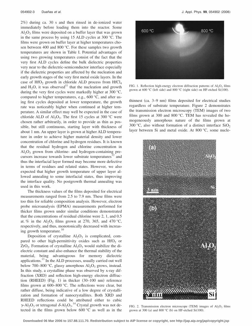
Deposition of crystalline Al2O3 is complicated, com-pared to other high-permittivity oxides such as HfO2 orZrO2. Formation of crystalline Al2O3 would stabilize the di-electric constant and also enhance the thermal stability of thematerial, being advantageous for memory dielectricapplications.13 In the ALD processes, usually carried out wellbelow 700–800 °C, glassy amorphous Al2O3 grows, instead.In this study, a crystalline phase was observed by x-ray dif-fraction �XRD� and reflection high-energy electron diffrac-tion �RHEED� �Fig. 1� in thicker �30–100 nm� referencefilms grown at 600–800 °C. The reflections were clear, butrather diffuse, being indicative of a low degree of crystalli-zation and formation of nanocrystallites. Both XRD andRHEED reflections could be attributed either to cubic�-Al2O3 or tetragonal �-Al2O3.14 Crystal growth was not de-
tected in the films grown below 600 °C as well as in theDownloaded 06 Mar 2006 to 157.88.111.70. Redistribution subject to
thinnest �ca. 3–9 nm� films deposited for electrical studiesregardless of substrate temperature. Figure 2 demonstratesthe transmission electron microscopy �TEM� images of twofilms grown at 300 and 800 °C. TEM has revealed the ho-mogeneously amorphous nature of the films grown at300 °C, also without formation of a distinct interface SiO2
layer between Si and metal oxide. At 800 °C, some nucle-
FIG. 1. Reflection high-energy electron diffraction patterns of Al2O3 filmsgrown at 600 °C �left side� and 800 °C �right side� on HF-etched Si�100�.
FIG. 2. Transmission electron microscope �TEM� images of Al2O3 films
grown at 300 �a� and 800 °C �b� on HF-etched Si�100�.AIP license or copyright, see http://jap.aip.org/jap/copyright.jsp

054902-4 Dueñas et al. J. Appl. Phys. 99, 054902 �2006�
ation and structural ordering become visible. The crystalliteformation becomes obvious after exceeding some criticalthickness, which is not lower than that of the films grown forMOS structures and relevant for the electrical measurements.Some ordering, weak, but still noticeable when compared tofilms grown at 300 °C, may still be considered to occurcloser to the interface. Additionally, according to the x-rayreflection data,14 the films grown at TG�600 °C possessedmarkedly higher densities than those grown at lower tem-peratures. It is noteworthy that the films grown on Si at800 °C showed a more pronounced interface layer �Fig. 2�,although its composition remains unknown at this stage. Itcan be expected that a more defective interface probablyformed at higher temperatures destructively compensates thehigher degree of ordering and otherwise more stable struc-ture. These structural and compositional differences wouldbe reflected by the dielectric performance.
The area of Al dots deposited on Al2O3 films was0.204 mm2. The backsides of the silicon substrates wereetched in HF and metallized by evaporating the Al electrodesto provide nearly ohmic contact to silicon. The thickness ofthe Al electrodes was 120–150 nm on Al2O3 as well as onthe backside of the substrates and the electrodes were depos-ited using electron-beam evaporation in an oil-free vacuum.
III. RESULTS AND DISCUSSION
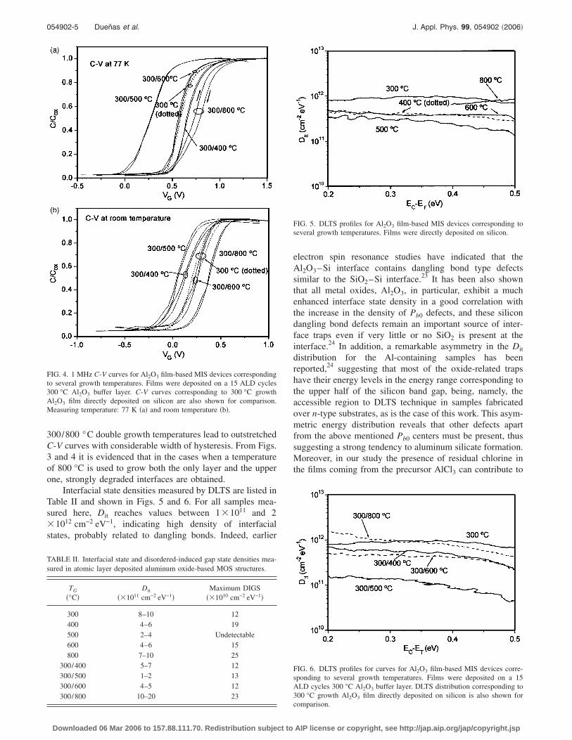
Figure 3 shows the 1 MHz C-V curves for Al2O3 film-based MIS devices corresponding to 300, 400, 500, 600, and800 °C growth temperatures measured at 77 K �a� and atroom temperature �b�. Curves measured at 77 K are shiftedtowards the positive voltage values in relation to those mea-sured at room temperature, suggesting that some thermallyactivated positive charge capture or negative charge releaseprocess has taken place. Afanas’ev et al.15,16 have calculatedthe metal/silicon work function difference �ms for both n-and p-type MOS structures with Al2O3 dielectric as a func-tion of gate metal electronegativity. For Al/Al2O3/n-Sistructures, they obtain �ms= +0.5 V. Flatband voltage valuesobtained for similar structures from our C-V measurementsare listed in Table I. We can see that at 77 K the lowestflatband voltage shift corresponds to 300, 400, and 500 °Cgrowth films. These films also have the lowest hysteresis.Sample grown at intermediate temperature �600 °C� exhibitssome negative flatband voltage shift, referring to the slightpresence of positive charge in the insulator bulk. Hydrogenin the charge state H+ could justify this positive charge.17
Hydrogen may serve as both deep donors in Al2O3 �Ref. 18�or a proton able to drift as ionic current.19 In the presentstudy, we observe relatively little hysteresis in the samplegrown at 600 °C, probably being indicative of only moderateeffect of residues.
In contrast, sample grown at 800 °C exhibits high posi-tive flatband voltage shift and great hysteresis behavior, in-dicating the presence of negative charge in the dielectriclayer and a poor interface quality. Negative charges possiblyare due to residual OH− ions.20 Indeed, using water as oxi-dant in the ALD process leaves residual hydrogen species in
10
the film, which could be tied up as OH groups. However,Downloaded 06 Mar 2006 to 157.88.111.70. Redistribution subject to
the density of surface OH groups as both active adsorptionsites and a source of residual hydrogen decreases withgrowth rate and hydrogen content with increasing tempera-ture in ALD process.12 The tetrahedrally coordinated Al3+ isbelieved to be another source of the negative charge.21 Theamorphous Al2O3 is quite defective, and crystallization inthin films is accompanied with densification due to the re-duction of free volume, i.e., vacancy type of defects in oxy-gen sublattice.22 In the present study, the results indicate thatthe partial crystallization observed in the films grown at el-evated temperature is not sufficient to entirely densify thematerial and improve its dielectric performance. On the con-trary, it can be thought that the chloride process applied atthat high temperature �800 °C� and without sufficiently thickbuffer layer may affect and deteriorate the quality of Si sur-face. This may be, for instance, a harmful side effect of sur-face reaction product HCl, or diffusion of chlorine throughthe underlayer and reaction with residual hydrogen, againforming HCl.
In Fig. 4, 1 MHz C-V curves measured at 77 K �a� and atroom temperature �b� corresponding to films deposited atseveral temperatures on the Al2O3 buffer layer �15 ALDcycles at 300 °C� are compared with samples grown only at300 °C. Flatband voltage and hysteresis values are listed inTable I. The growth of a second layer at 400, 500, or 600 °Cdoes not increase the stretch-out or hysteresis of C-V curves
FIG. 3. 1 MHz C-V curves for Al2O3 film-based MIS devices correspondingto several growth temperatures. Films were directly deposited on silicon.Measuring temperature: 77 K �a� and room temperature �b�.
considerably. However, in Fig. 4�a� we can see that
AIP license or copyright, see http://jap.aip.org/jap/copyright.jsp
054902-5 Dueñas et al. J. Appl. Phys. 99, 054902 �2006�
300/800 °C double growth temperatures lead to outstretchedC-V curves with considerable width of hysteresis. From Figs.3 and 4 it is evidenced that in the cases when a temperatureof 800 °C is used to grow both the only layer and the upperone, strongly degraded interfaces are obtained.
Interfacial state densities measured by DLTS are listed inTable II and shown in Figs. 5 and 6. For all samples mea-sured here, Dit reaches values between 1�1011 and 2�1012 cm−2 eV−1, indicating high density of interfacialstates, probably related to dangling bonds. Indeed, earlier
FIG. 4. 1 MHz C-V curves for Al2O3 film-based MIS devices correspondingto several growth temperatures. Films were deposited on a 15 ALD cycles300 °C Al2O3 buffer layer. C-V curves corresponding to 300 °C growthAl2O3 film directly deposited on silicon are also shown for comparison.Measuring temperature: 77 K �a� and room temperature �b�.
TABLE II. Interfacial state and disordered-induced gap state densities mea-sured in atomic layer deposited aluminum oxide-based MOS structures.
TG
�°C�Dit
��1011 cm−2 eV−1�Maximum DIGS
��1010 cm−2 eV−1�
300 8–10 12400 4–6 19500 2–4 Undetectable600 4–6 15800 7–10 25
300/400 5–7 12300/500 1–2 13300/600 4–5 12300/800 10–20 23
Downloaded 06 Mar 2006 to 157.88.111.70. Redistribution subject to
electron spin resonance studies have indicated that theAl2O3–Si interface contains dangling bond type defectssimilar to the SiO2–Si interface.23 It has been also shownthat all metal oxides, Al2O3, in particular, exhibit a muchenhanced interface state density in a good correlation withthe increase in the density of Pb0 defects, and these silicondangling bond defects remain an important source of inter-face traps even if very little or no SiO2 is present at theinterface.24 In addition, a remarkable asymmetry in the Dit
distribution for the Al-containing samples has beenreported,24 suggesting that most of the oxide-related trapshave their energy levels in the energy range corresponding tothe upper half of the silicon band gap, being, namely, theaccessible region to DLTS technique in samples fabricatedover n-type substrates, as is the case of this work. This asym-metric energy distribution reveals that other defects apartfrom the above mentioned Pb0 centers must be present, thussuggesting a strong tendency to aluminum silicate formation.Moreover, in our study the presence of residual chlorine inthe films coming from the precursor AlCl3 can contribute to
FIG. 5. DLTS profiles for Al2O3 film-based MIS devices corresponding toseveral growth temperatures. Films were directly deposited on silicon.
FIG. 6. DLTS profiles for curves for Al2O3 film-based MIS devices corre-sponding to several growth temperatures. Films were deposited on a 15ALD cycles 300 °C Al2O3 buffer layer. DLTS distribution corresponding to300 °C growth Al2O3 film directly deposited on silicon is also shown for
comparison.AIP license or copyright, see http://jap.aip.org/jap/copyright.jsp

054902-6 Dueñas et al. J. Appl. Phys. 99, 054902 �2006�
the interface electrical characteristics, inducing extra bandgap levels and so creating interfacial states.25
As for the influence of growth temperature on the inter-facial state density, Fig. 5 shows that 300 and 800 °Cgrowth temperatures provide Dit values of about 1�1012 cm−2 eV−1. In contrast, intermediate temperature val-ues �400, 500, and 600 °C� provide lower values of Dit
�about �3–5��1011 cm−2 eV−1�. In Fig. 6 films deposited atseveral temperatures on a 15 ALD cycles 300 °C Al2O3
buffer layer are compared with samples grown at 300 °C.Clearly, combining the growth temperatures 300/800 °Cdoes not diminish the interfacial state density, whereas tem-peratures 300/400 and 300/600 °C improve interface qual-ity in terms of Dit �Dit goes down to about �4–7��1011 cm−2 eV−1�. The best combination has been300/500 °C, providing Dit values as low as �1–2��1011 cm−2 eV−1. These results are in good agreement withthe C-V results described above.
In order to evaluate the interface quality, another impor-tant concern is the distribution of disorder-induced gap states�DIGS�, i.e., the density of states distributed at some distancefrom the interface to the insulator.26 As it has been described
FIG. 7. Three-dimensional DIGS profiles corresponding to 300 �a�, 400 �b�, 6deposited on silicon.
elsewhere, it is possible to obtain three-dimensional plots of
Downloaded 06 Mar 2006 to 157.88.111.70. Redistribution subject to
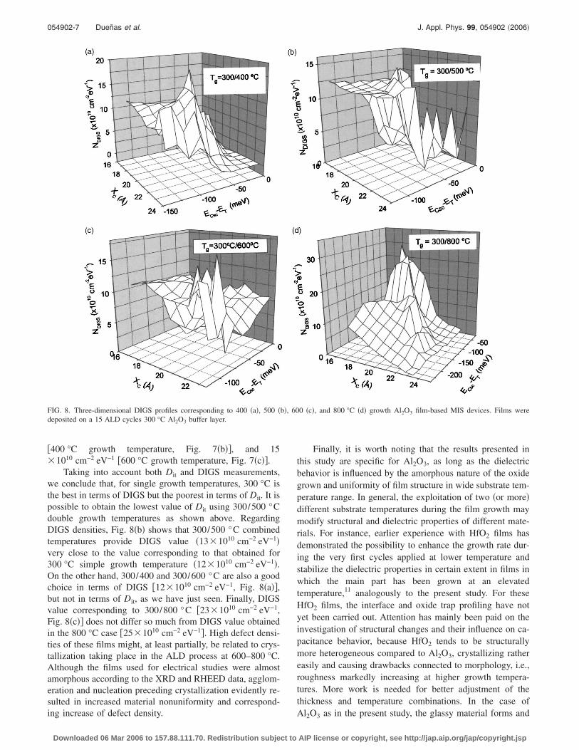
DIGS density as a function of the energy position and of thespatial distance to the interface from conductance-transientmeasurements.27,28 Figures 7 and 8 show these plots forsingle and double growth temperatures, respectively. Themaxima of the DIGS profiles from Figs. 7 and 8 are indi-cated in the third column of Table II. Among samples grownat single temperatures, 300 °C provides the lowest DIGSvalue recorded �12�1010 cm−2 eV−1, Fig. 7�a��, whereas to800 °C corresponds so high value as 25�1010 cm−2 eV−1
�Fig. 5�. Sample deposited at 500 °C occurred unmeasurablein terms of DIGS. The reason for this remains somewhatunclear at this moment. It is quite possible that this wide-gapmaterial, Al2O3, grown at this temperature is despite theamorphicity already very pure and free of residual defects, inaddition to the highest structural homogeneity achieved andtherefore the defect densities may be low enough not tocause well measurable conductivity signal. However, somecare must be taken before concluding the perfection of thematerial, because very high defect concentrations sometimesallowed in other materials, such as Nb oxides, might causequick discharging of the defect states and technically unmea-surable DIGS. Intermediate growth temperatures generally
10 −2 −1
�, and 800 °C �d� growth Al2O3 film-based MIS devices. Films were directly
00 �clead to intermediate DIGS values: 19�10 cm eV
AIP license or copyright, see http://jap.aip.org/jap/copyright.jsp
054902-7 Dueñas et al. J. Appl. Phys. 99, 054902 �2006�
�400 °C growth temperature, Fig. 7�b��, and 15�1010 cm−2 eV−1 �600 °C growth temperature, Fig. 7�c��.
Taking into account both Dit and DIGS measurements,we conclude that, for single growth temperatures, 300 °C isthe best in terms of DIGS but the poorest in terms of Dit. It ispossible to obtain the lowest value of Dit using 300/500 °Cdouble growth temperatures as shown above. RegardingDIGS densities, Fig. 8�b� shows that 300/500 °C combinedtemperatures provide DIGS value �13�1010 cm−2 eV−1�very close to the value corresponding to that obtained for300 °C simple growth temperature �12�1010 cm−2 eV−1�.On the other hand, 300/400 and 300/600 °C are also a goodchoice in terms of DIGS �12�1010 cm−2 eV−1, Fig. 8�a��,but not in terms of Dit, as we have just seen. Finally, DIGSvalue corresponding to 300/800 °C �23�1010 cm−2 eV−1,Fig. 8�c�� does not differ so much from DIGS value obtainedin the 800 °C case �25�1010 cm−2 eV−1�. High defect densi-ties of these films might, at least partially, be related to crys-tallization taking place in the ALD process at 600–800 °C.Although the films used for electrical studies were almostamorphous according to the XRD and RHEED data, agglom-eration and nucleation preceding crystallization evidently re-sulted in increased material nonuniformity and correspond-
FIG. 8. Three-dimensional DIGS profiles corresponding to 400 �a�, 500 �deposited on a 15 ALD cycles 300 °C Al2O3 buffer layer.
ing increase of defect density.
Downloaded 06 Mar 2006 to 157.88.111.70. Redistribution subject to
Finally, it is worth noting that the results presented inthis study are specific for Al2O3, as long as the dielectricbehavior is influenced by the amorphous nature of the oxidegrown and uniformity of film structure in wide substrate tem-perature range. In general, the exploitation of two �or more�different substrate temperatures during the film growth maymodify structural and dielectric properties of different mate-rials. For instance, earlier experience with HfO2 films hasdemonstrated the possibility to enhance the growth rate dur-ing the very first cycles applied at lower temperature andstabilize the dielectric properties in certain extent in films inwhich the main part has been grown at an elevatedtemperature,11 analogously to the present study. For theseHfO2 films, the interface and oxide trap profiling have notyet been carried out. Attention has mainly been paid on theinvestigation of structural changes and their influence on ca-pacitance behavior, because HfO2 tends to be structurallymore heterogeneous compared to Al2O3, crystallizing rathereasily and causing drawbacks connected to morphology, i.e.,roughness markedly increasing at higher growth tempera-tures. More work is needed for better adjustment of thethickness and temperature combinations. In the case of
0 �c�, and 800 °C �d� growth Al2O3 film-based MIS devices. Films were
b�, 60Al2O3 as in the present study, the glassy material forms and
AIP license or copyright, see http://jap.aip.org/jap/copyright.jsp
054902-8 Dueñas et al. J. Appl. Phys. 99, 054902 �2006�
better allows the investigation of the electric properties inwider substrate temperature range compared to HfO2.
IV. CONCLUSIONS
Electrical characterization of Al2O3 based MIS struc-tures has been carried out. Dielectric films were atomic layerdeposited at temperatures ranging from 300 to 800 °C eitherdirectly on silicon substrates or on an Al2O3 buffer layergrown in the same process by using 15 ALD cycles at300 °C. As the very first ALD cycles influence the bulk di-electric properties very near to the dielectric-semiconductorinterface, an upper layer grown at higher ALD temperatureprobably anneals some interfacial states, thus improving theinterface quality.
Our experimental data indicate that the sample formedafter 15 cycles deposited at 300 °C followed by 120 cyclesdeposited at 500 °C showed the lowest interface state��1–2��1011 cm−2 eV−1� and quite low DIGS �13�1010 cm−2 eV−1� densities. Exploitation of double tempera-tures 300/400 and 300/600 °C also provided low values ofDIGS density, although interfacial state density was close tothe value measured when using a simple growth temperatureof 300 °C. So, 300/500 °C has been a better choice than300/400 and 300/600 °C double temperature depositions. Incontrast, samples in which either the entire dielectric film orone upper layer was grown at the highest temperature�800 °C� have shown the poorest result in terms of flatbandvoltage shift and amount of hysteresis, also in terms of inter-face state density ��1–2��1012 cm−2 eV−1� and DIGS��23–25��1010 cm−2 eV−1�. That suggests to us that usingvery high growth temperature such as 800 °C yield defectivedielectric films.
ACKNOWLEDGMENTS
The study was partially supported by the Spanish DGE-SIC under Grant No. BFM 2001-2250, Estonian ScienceFoundation �Grant No. 5861�, and European CommissionHuman Potential Programme Access to Research Infrastruc-
tures.Downloaded 06 Mar 2006 to 157.88.111.70. Redistribution subject to
1J. Robertson, MRS Bull. 27, 217 �2002�.2G. D. Wilk, R. M. Wallace, and J. M. Anthony, J. Appl. Phys. 89, 5243�2001�.
3J. Robertson, Eur. Phys. J.: Appl. Phys. 28, 265 �2004�.4T. Suntola, Mater. Sci. Rep. 4, 261 �1989�.5M. Ritala and M. Leskelä, in Handbook of Thin Film Materials, Deposi-tion and Processing of Thin Film Materials Vol. 1, edited by H. S. Nalwa�Academic, San Diego, 2002�, p. 104.
6G. S. Higashi and C. G. Flemming, Appl. Phys. Lett. 55, 1963 �1989�.7M. Ritala, in High-k Gate Dielectrics, Materials Science and EngineeringSeries, edited by M. Houssa �IOP, London, 2004�, p. 17.
8J. Aarik, A. Aidla, H. Mändar, V. Sammelselg, and T. Uustare, J. Cryst.Growth 220, 105 �2000�.
9J. Aarik, A. Aidla, A. Jaek, A.-A. Kiisler, and A.-A. Tammik, Acta Poly-tech. Scand. 195, 201 �1990�.
10J. Aarik, A. Aidla, and K. Kukli, Appl. Surf. Sci. 75, 180 �1994�.11K. Kukli et al., Thin Solid Films 479, 1 �2005�.12K. Kukli, M. Ritala, M. Leskelä, and J. Jokinen, J. Vac. Sci. Technol. A
15, 2214 �1997�.13S. Jakschik, U. Schroeder, T. Hecht, G. Dollinger, A. Bergmaier, and J. W.
Bartha, Mater. Sci. Eng., B B107, 251 �2004�.14J. Aarik, A. Kasikov, M. Kirm, S. Lange, T. Uustare, and H. Mändar,
Proc. SPIE 5946, 594601-1 �2005�.15V. V. Afanas’ev, M. Houssa, A. Stesmans, and M. M. Heyns, J. Appl.
Phys. 91, 3079 �2002�.16V. V. Afanas’ev, M. Houssa, A. Stesmans, G. J. Adriaenssens, and M. M.
Heyns, J. Non-Cryst. Solids 303, 69 �2002�.17P. W. Peacock and J. Robertson, Appl. Phys. Lett. 83, 2025 �2003�.18J. Robertson and P. W. Peacock, Microelectron. Eng. 72, 112 �2004�.19J. F. Zhang, C. Z. Zhao, G. Groeseneken, R. Degraeve, J. N. Ellis, and C.
D. Beech, J. Appl. Phys. 90, 1911 �2001�.20I. S. Jeon, J. Park, and D. Eom, Jpn. J. Appl. Phys., Part 1 42, 1222
�2003�.21V. Mikhelashvili, B. Meyler, J. Shneider, O. Kreinin, and G. Eisenstein,
Microelectron. Reliab. 45, 933 �2005�.22P. C. Snijders, L. P. H. Jeurgens, and W. G. Sloof, Surf. Sci. 589, 98
�2005�.23A. Stesmans and V. V. Afanas’ev, Appl. Phys. Lett. 80, 1957 �2002�.24L. Truong, Y. G. Fedorenko, V. V. Afanas’ev, and A. Stesmans, Micro-
electron. Reliab. 45, 823 �2005�.25S. Ferrari, G. Scarel, C. Wiemer, and M. Fanciulli, J. Appl. Phys. 92, 7675
�2002�.26L. He, H. Hasegawa, T. Sawada, and H. Ohno, J. Appl. Phys. 63, 2120
�1988�.27S. Dueñas, R. Peláez, H. Castán, R. Pinacho, L. Quintanilla, J. Barbolla, I.
Mártil, and G. González-Díaz, Appl. Phys. Lett. 71, 826 �1997�.28H. Castán, S. Dueñas, J. Barbolla, E. Redondo, N. Blanco, I. Mártil, and
G. González-Díaz, Microelectron. Reliab. 40, 845 �2000�.
AIP license or copyright, see http://jap.aip.org/jap/copyright.jsp