Influence of Cu as a catalyst on the properties of silicon nanowires synthesized by the...
8
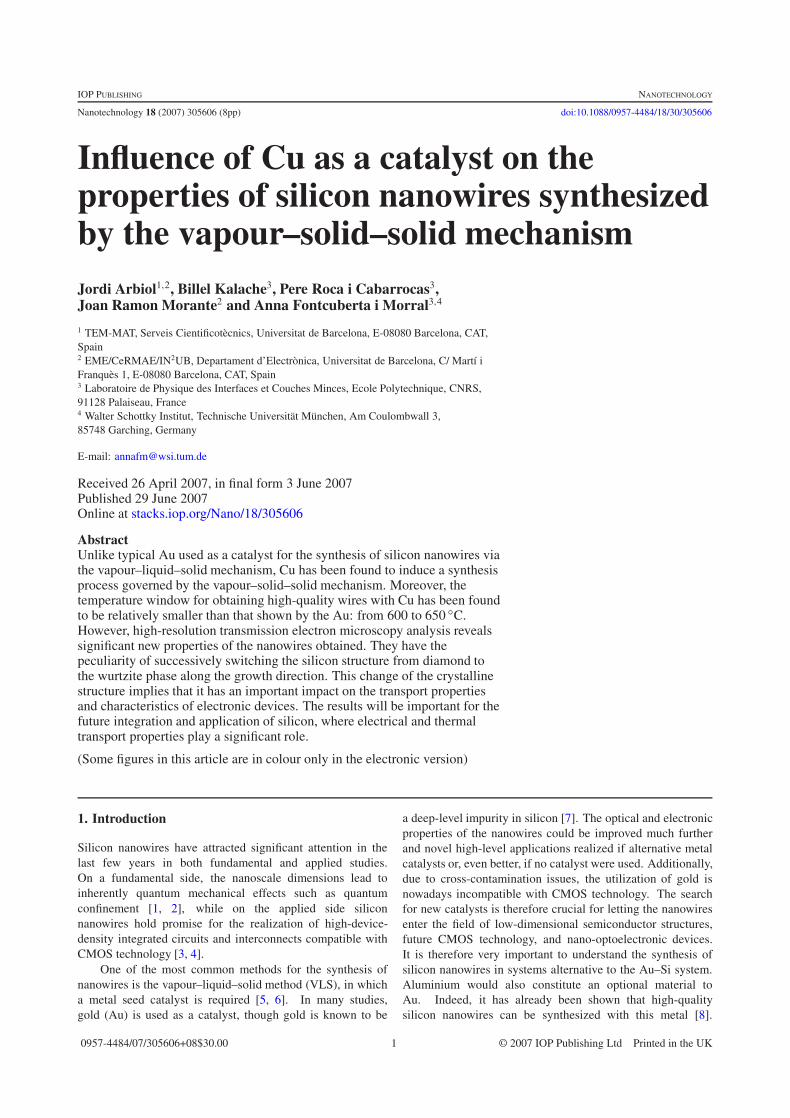
IOP PUBLISHING NANOTECHNOLOGY Nanotechnology 18 (2007) 305606 (8pp) doi:10.1088/0957-4484/18/30/305606 Influence of Cu as a catalyst on the properties of silicon nanowires synthesized by the vapour–solid–solid mechanism Jordi Arbiol 1,2 , Billel Kalache 3 , Pere Roca i Cabarrocas 3 , Joan Ramon Morante 2 and Anna Fontcuberta i Morral 3,4 1 TEM-MAT, Serveis Cientificot` ecnics, Universitat de Barcelona, E-08080 Barcelona, CAT, Spain 2 EME/CeRMAE/IN 2 UB, Departament d’Electr` onica, Universitat de Barcelona, C/ Mart´ ıi Franqu` es 1, E-08080 Barcelona, CAT, Spain 3 Laboratoire de Physique des Interfaces et Couches Minces, Ecole Polytechnique, CNRS, 91128 Palaiseau, France 4 Walter Schottky Institut, Technische Universit¨ at M¨ unchen, Am Coulombwall 3, 85748 Garching, Germany E-mail: [email protected] Received 26 April 2007, in final form 3 June 2007 Published 29 June 2007 Online at stacks.iop.org/Nano/18/305606 Abstract Unlike typical Au used as a catalyst for the synthesis of silicon nanowires via the vapour–liquid–solid mechanism, Cu has been found to induce a synthesis process governed by the vapour–solid–solid mechanism. Moreover, the temperature window for obtaining high-quality wires with Cu has been found to be relatively smaller than that shown by the Au: from 600 to 650 ◦ C. However, high-resolution transmission electron microscopy analysis reveals significant new properties of the nanowires obtained. They have the peculiarity of successively switching the silicon structure from diamond to the wurtzite phase along the growth direction. This change of the crystalline structure implies that it has an important impact on the transport properties and characteristics of electronic devices. The results will be important for the future integration and application of silicon, where electrical and thermal transport properties play a significant role. (Some figures in this article are in colour only in the electronic version) 1. Introduction Silicon nanowires have attracted significant attention in the last few years in both fundamental and applied studies. On a fundamental side, the nanoscale dimensions lead to inherently quantum mechanical effects such as quantum confinement [1, 2], while on the applied side silicon nanowires hold promise for the realization of high-device- density integrated circuits and interconnects compatible with CMOS technology [3, 4]. One of the most common methods for the synthesis of nanowires is the vapour–liquid–solid method (VLS), in which a metal seed catalyst is required [5, 6]. In many studies, gold (Au) is used as a catalyst, though gold is known to be a deep-level impurity in silicon [7]. The optical and electronic properties of the nanowires could be improved much further and novel high-level applications realized if alternative metal catalysts or, even better, if no catalyst were used. Additionally, due to cross-contamination issues, the utilization of gold is nowadays incompatible with CMOS technology. The search for new catalysts is therefore crucial for letting the nanowires enter the field of low-dimensional semiconductor structures, future CMOS technology, and nano-optoelectronic devices. It is therefore very important to understand the synthesis of silicon nanowires in systems alternative to the Au–Si system. Aluminium would also constitute an optional material to Au. Indeed, it has already been shown that high-quality silicon nanowires can be synthesized with this metal [8]. 0957-4484/07/305606+08$30.00 1 © 2007 IOP Publishing Ltd Printed in the UK
-
Upload
polytechnique -
Category
Documents
-
view
4 -
download
0
Transcript of Influence of Cu as a catalyst on the properties of silicon nanowires synthesized by the...
IOP PUBLISHING NANOTECHNOLOGY
Nanotechnology 18 (2007) 305606 (8pp) doi:10.1088/0957-4484/18/30/305606
Influence of Cu as a catalyst on theproperties of silicon nanowires synthesizedby the vapour–solid–solid mechanismJordi Arbiol1,2, Billel Kalache3, Pere Roca i Cabarrocas3,Joan Ramon Morante2 and Anna Fontcuberta i Morral3,4
1 TEM-MAT, Serveis Cientificotecnics, Universitat de Barcelona, E-08080 Barcelona, CAT,Spain2 EME/CeRMAE/IN2UB, Departament d’Electronica, Universitat de Barcelona, C/ Martı iFranques 1, E-08080 Barcelona, CAT, Spain3 Laboratoire de Physique des Interfaces et Couches Minces, Ecole Polytechnique, CNRS,91128 Palaiseau, France4 Walter Schottky Institut, Technische Universitat Munchen, Am Coulombwall 3,85748 Garching, Germany
E-mail: [email protected]
Received 26 April 2007, in final form 3 June 2007Published 29 June 2007Online at stacks.iop.org/Nano/18/305606
AbstractUnlike typical Au used as a catalyst for the synthesis of silicon nanowires viathe vapour–liquid–solid mechanism, Cu has been found to induce a synthesisprocess governed by the vapour–solid–solid mechanism. Moreover, thetemperature window for obtaining high-quality wires with Cu has been foundto be relatively smaller than that shown by the Au: from 600 to 650 ◦C.However, high-resolution transmission electron microscopy analysis revealssignificant new properties of the nanowires obtained. They have thepeculiarity of successively switching the silicon structure from diamond tothe wurtzite phase along the growth direction. This change of the crystallinestructure implies that it has an important impact on the transport propertiesand characteristics of electronic devices. The results will be important for thefuture integration and application of silicon, where electrical and thermaltransport properties play a significant role.
(Some figures in this article are in colour only in the electronic version)
1. Introduction
Silicon nanowires have attracted significant attention in thelast few years in both fundamental and applied studies.On a fundamental side, the nanoscale dimensions lead toinherently quantum mechanical effects such as quantumconfinement [1, 2], while on the applied side siliconnanowires hold promise for the realization of high-device-density integrated circuits and interconnects compatible withCMOS technology [3, 4].
One of the most common methods for the synthesis ofnanowires is the vapour–liquid–solid method (VLS), in whicha metal seed catalyst is required [5, 6]. In many studies,gold (Au) is used as a catalyst, though gold is known to be
a deep-level impurity in silicon [7]. The optical and electronicproperties of the nanowires could be improved much furtherand novel high-level applications realized if alternative metalcatalysts or, even better, if no catalyst were used. Additionally,due to cross-contamination issues, the utilization of gold isnowadays incompatible with CMOS technology. The searchfor new catalysts is therefore crucial for letting the nanowiresenter the field of low-dimensional semiconductor structures,future CMOS technology, and nano-optoelectronic devices.It is therefore very important to understand the synthesis ofsilicon nanowires in systems alternative to the Au–Si system.Aluminium would also constitute an optional material toAu. Indeed, it has already been shown that high-qualitysilicon nanowires can be synthesized with this metal [8].
0957-4484/07/305606+08$30.00 1 © 2007 IOP Publishing Ltd Printed in the UK
Nanotechnology 18 (2007) 305606 J Arbiol et al
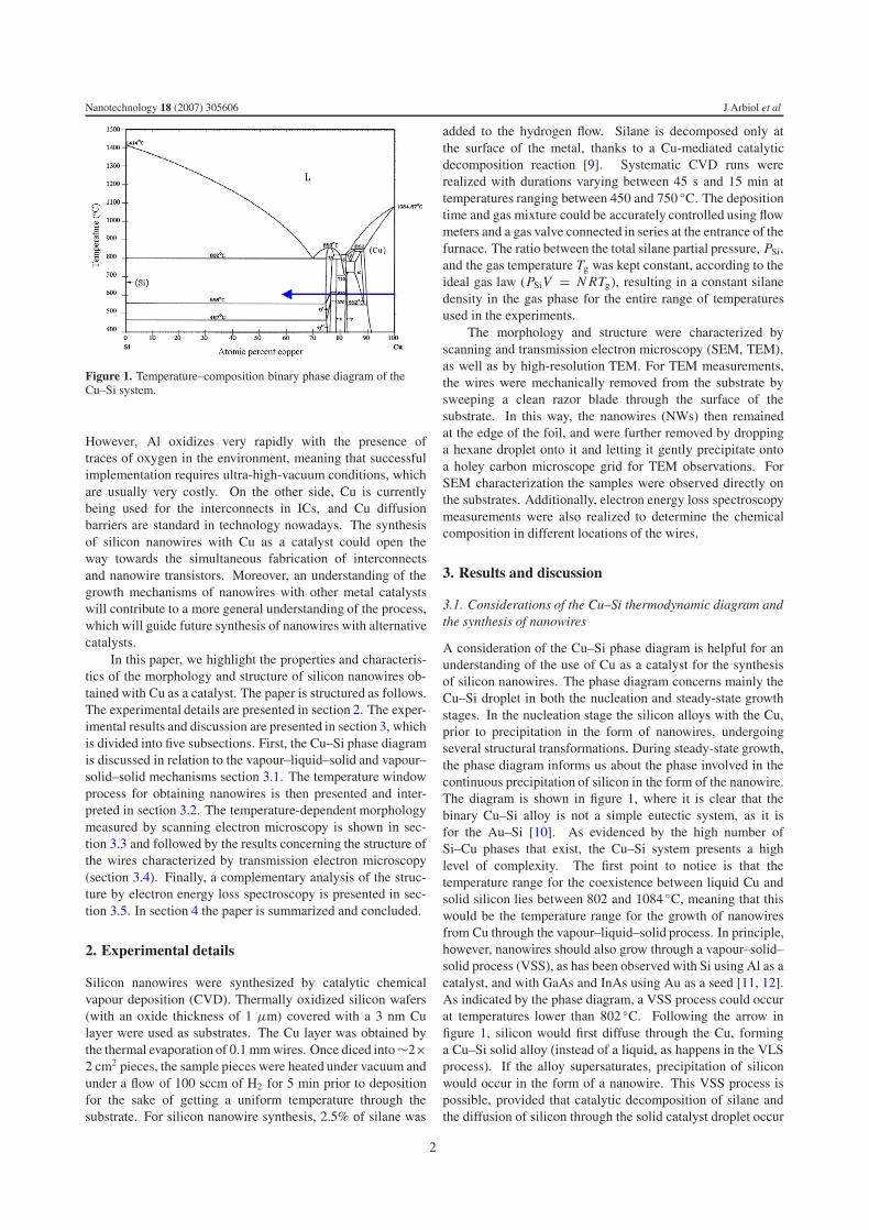
Figure 1. Temperature–composition binary phase diagram of theCu–Si system.
However, Al oxidizes very rapidly with the presence oftraces of oxygen in the environment, meaning that successfulimplementation requires ultra-high-vacuum conditions, whichare usually very costly. On the other side, Cu is currentlybeing used for the interconnects in ICs, and Cu diffusionbarriers are standard in technology nowadays. The synthesisof silicon nanowires with Cu as a catalyst could open theway towards the simultaneous fabrication of interconnectsand nanowire transistors. Moreover, an understanding of thegrowth mechanisms of nanowires with other metal catalystswill contribute to a more general understanding of the process,which will guide future synthesis of nanowires with alternativecatalysts.
In this paper, we highlight the properties and characteris-tics of the morphology and structure of silicon nanowires ob-tained with Cu as a catalyst. The paper is structured as follows.The experimental details are presented in section 2. The exper-imental results and discussion are presented in section 3, whichis divided into five subsections. First, the Cu–Si phase diagramis discussed in relation to the vapour–liquid–solid and vapour–solid–solid mechanisms section 3.1. The temperature windowprocess for obtaining nanowires is then presented and inter-preted in section 3.2. The temperature-dependent morphologymeasured by scanning electron microscopy is shown in sec-tion 3.3 and followed by the results concerning the structure ofthe wires characterized by transmission electron microscopy(section 3.4). Finally, a complementary analysis of the struc-ture by electron energy loss spectroscopy is presented in sec-tion 3.5. In section 4 the paper is summarized and concluded.
2. Experimental details
Silicon nanowires were synthesized by catalytic chemicalvapour deposition (CVD). Thermally oxidized silicon wafers(with an oxide thickness of 1 μm) covered with a 3 nm Culayer were used as substrates. The Cu layer was obtained bythe thermal evaporation of 0.1 mm wires. Once diced into ∼2×2 cm2 pieces, the sample pieces were heated under vacuum andunder a flow of 100 sccm of H2 for 5 min prior to depositionfor the sake of getting a uniform temperature through thesubstrate. For silicon nanowire synthesis, 2.5% of silane was
added to the hydrogen flow. Silane is decomposed only atthe surface of the metal, thanks to a Cu-mediated catalyticdecomposition reaction [9]. Systematic CVD runs wererealized with durations varying between 45 s and 15 min attemperatures ranging between 450 and 750 ◦C. The depositiontime and gas mixture could be accurately controlled using flowmeters and a gas valve connected in series at the entrance of thefurnace. The ratio between the total silane partial pressure, PSi,and the gas temperature Tg was kept constant, according to theideal gas law (PSiV = N RTg), resulting in a constant silanedensity in the gas phase for the entire range of temperaturesused in the experiments.
The morphology and structure were characterized byscanning and transmission electron microscopy (SEM, TEM),as well as by high-resolution TEM. For TEM measurements,the wires were mechanically removed from the substrate bysweeping a clean razor blade through the surface of thesubstrate. In this way, the nanowires (NWs) then remainedat the edge of the foil, and were further removed by droppinga hexane droplet onto it and letting it gently precipitate ontoa holey carbon microscope grid for TEM observations. ForSEM characterization the samples were observed directly onthe substrates. Additionally, electron energy loss spectroscopymeasurements were also realized to determine the chemicalcomposition in different locations of the wires.
3. Results and discussion
3.1. Considerations of the Cu–Si thermodynamic diagram andthe synthesis of nanowires
A consideration of the Cu–Si phase diagram is helpful for anunderstanding of the use of Cu as a catalyst for the synthesisof silicon nanowires. The phase diagram concerns mainly theCu–Si droplet in both the nucleation and steady-state growthstages. In the nucleation stage the silicon alloys with the Cu,prior to precipitation in the form of nanowires, undergoingseveral structural transformations. During steady-state growth,the phase diagram informs us about the phase involved in thecontinuous precipitation of silicon in the form of the nanowire.The diagram is shown in figure 1, where it is clear that thebinary Cu–Si alloy is not a simple eutectic system, as it isfor the Au–Si [10]. As evidenced by the high number ofSi–Cu phases that exist, the Cu–Si system presents a highlevel of complexity. The first point to notice is that thetemperature range for the coexistence between liquid Cu andsolid silicon lies between 802 and 1084 ◦C, meaning that thiswould be the temperature range for the growth of nanowiresfrom Cu through the vapour–liquid–solid process. In principle,however, nanowires should also grow through a vapour–solid–solid process (VSS), as has been observed with Si using Al as acatalyst, and with GaAs and InAs using Au as a seed [11, 12].As indicated by the phase diagram, a VSS process could occurat temperatures lower than 802 ◦C. Following the arrow infigure 1, silicon would first diffuse through the Cu, forminga Cu–Si solid alloy (instead of a liquid, as happens in the VLSprocess). If the alloy supersaturates, precipitation of siliconwould occur in the form of a nanowire. This VSS process ispossible, provided that catalytic decomposition of silane andthe diffusion of silicon through the solid catalyst droplet occur
2

Nanotechnology 18 (2007) 305606 J Arbiol et al
at a similar rate. In figure 1, an arrow has been drawn to followthe composition of a Cu droplet exposed to silicon diffusion.This arrow indicates the phase transformations of the Cu–Sialloy as the silicon content increases, which would be theprocess that the Cu droplet would follow during the nucleationof nanowires. As silicon diffuses through the Cu droplet, firstCu5Si (phases ε and γ ) is formed. Then, as more silicondiffuses in and its content increases, Cu3Si starts to form. Byfurther increasing the silicon content of the seed, silicon finallyprecipitates from Cu3Si. Depending on the temperature, thefinal phase from which the nanowires would precipitate wouldbe one of the three different forms of Cu3Si: η′′, η′ or η. Adetailed study on the phase transformations occurring in thecatalyst droplet prior to nanowire nucleation would give furtherinsight into the dynamic aspects of the phase transformationspresented. It is important to note that the three different Cu3Sisolid phases have a distinct crystalline structure, which mighthave an influence on the final structure and morphology of theprecipitates. It should also be noted that the phase diagramapplies to bulk Cu–Si alloys in thermodynamic equilibrium,and that certain deviations should be expected for reduced alloyvolumes and under dynamic conditions (growth).
3.2. Temperature process window for nanowire synthesis
For determining the temperature dependence, Cu nanodropletswere exposed to silane at temperatures between 450 and750 ◦C. Nanowires were obtained at temperatures between 500and 650 ◦C. According to the phase diagram presented above,the synthesis of nanowires from Cu in this temperature rangeis consistent only through the VSS mechanism.
The low-temperature limit of 500 ◦C could be attributedto the absence of silane decomposition. However, it has beenreported that silane decomposes catalytically at the surface ofcopper through the VSS process at temperatures as low as230 ◦C, invalidating this first hypothesis [13]. We believe thatthe low-temperature limit should rather be attributed to thelow value of the diffusion coefficient of silicon through Cu3Si,in comparison to the decomposition rate of silane on the Cusurface. Indeed, it has recently been shown that the incubationtime, defined as the time necessary for the catalyst to reachsuper-saturation leading to the growth of nanowires, followsthe form [14]:
τ ≈ h2
〈DSO〉 exp (−Ea/K T )(1)
where h is the height of the catalyst nanoparticle, DSO is relatedto the pre-factor of the diffusion coefficient of silicon throughCu3Si, and Ea corresponds to its activation energy. Theactivation energy for the Cu–Si system is 0.98 eV, which meansthat, for 10 nm catalyst droplets, the incubation times wouldincrease, for example, from 100 to 400 s when decreasing thesynthesis temperature from 500 to 450 ◦C. We propose that thefollowing happens at lower temperatures. As a consequence ofthe low values of the coefficient of diffusion of silicon throughCu, there is early silicon super-saturation at the surface of theCu seed prior to reaching the equilibrium in the whole catalyst.A silicon shell is formed, stopping the further decompositionof silane at the surface of the nanoparticle and therefore thenanowire nucleation.
On the other hand, the growth of silicon nanowires attemperatures higher than 650 ◦C is limited by a differentreason. Our SEM measurements indicate that the surfaceof the substrate is flat after the CVD run and no dropletsare formed. We believe that this is due to the diffusion ofcopper through the SiO2. Indeed, diffusion of copper throughSiO2 has an activation energy of 1.82 eV, which is muchhigher than the activation energy for diffusion of Si throughCu3Si (0.98 eV) [15]. This means that, in a certain range oftemperatures, the diffusion coefficient of silicon through Cu3Sican be higher than the coefficient of diffusion of Cu throughSiO2, allowing the nucleation of silicon nanowires. However,the large value of the activation energy also means that theremust be a temperature above which the diffusion of Cu throughSiO2 occurs at a higher rate than the diffusion of Si throughCu3Si. This temperature is situated slightly above 650 ◦C,and this is the reason for the lack of nanowire synthesis. Forthe synthesis of nanowires in higher-temperature regimes, Cudiffusion barriers should be used.
3.3. Temperature dependence of the morphology
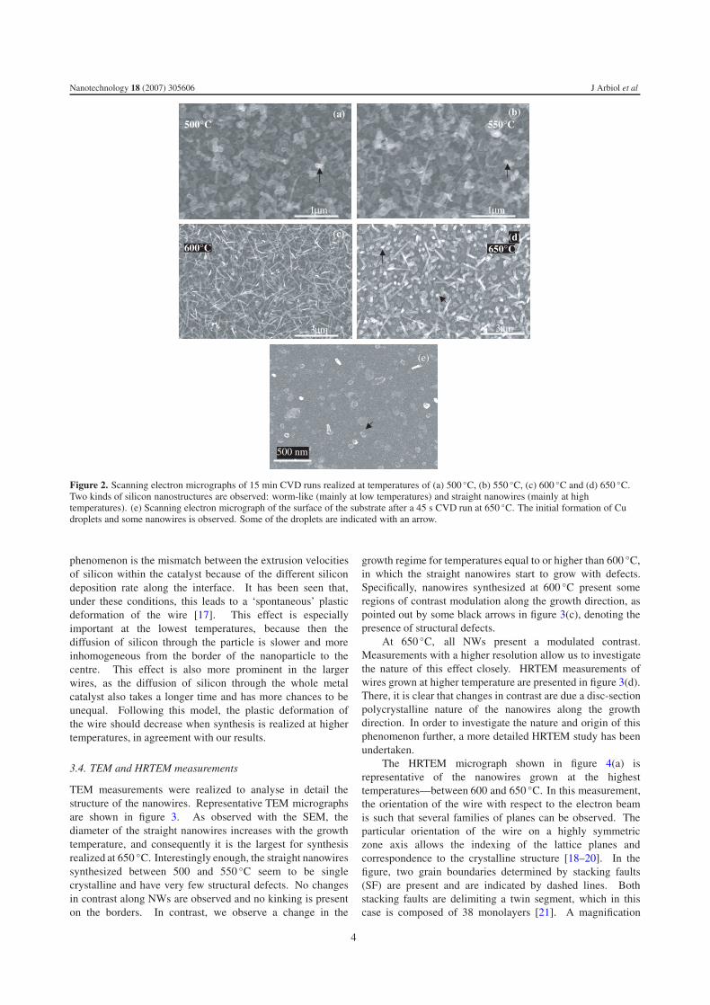
CVD runs were realized from 450 to 750 ◦C on Cu-coatedsilicon oxidized substrates. After the CVD runs, thesamples were first observed using SEM. Representative SEMmicrographs of the synthesis realized between 500 and 650 ◦Care presented in figure 2. Figures 2(a)–(d) correspond to a15 min synthesis (steady-state growth). Figure 2(e) showsthe morphology of the substrate at the initial stage of Cudroplet formation and nanowire nucleation, corresponding toa 45 s process at 650 ◦C. As it appears in the micrographs,the morphology is dramatically dependent on the temperatureof synthesis. In general, two features co-exist: worm-like nanostructures and straight nanowires. The worm-likestructures are nanowires with a diameter of about 100 nmthat seem to have been growing with a continuous kinking.The other nanowires show a completely different morphology.They are thinner and grow straight with very little kinking.Two-dimensional film growth on the substrate has not beenobserved at any of the temperatures. At 500 ◦C, the worm-like structures are predominant and very few straight nanowiresexist. As the synthesis temperature is increased, the ratioof worm-like nanostructures to nanowires decreases to theextent that at 600 ◦C they have nearly disappeared. At650 ◦C, no worm-like wires were observed. The diameterof the straight nanowires also changes with temperature. At500 ◦C and 650 ◦C, the diameters are respectively about 10 nmand 100 nm. At 650 ◦C, nanowires exhibit another specificcharacteristic, which is that they appear significantly tapered.As the decomposition of silane at 650 ◦C occurs only at thesurface of the metal catalyst, the tapering indicates that thecopper is being ‘consumed’ during growth, by dissolving intothe wires. Tapering could imply dissolution of the Cu intothe wires during growth and therefore we have detrimentalconsequences on the properties of the wires, but, as has alreadybeen shown for Au, this could also imply migration of the Cuto neighbouring wire tips [16].
The origin of the worm-like nanowires can be understoodin terms of the spatial-velocity hodograph concept, whichwas first observed in carbon nanotubes. The origin of this
3
Nanotechnology 18 (2007) 305606 J Arbiol et al
(a) (b)500°C 550°
C
1µm 1µm
(c) (d) 650°C
3µm 3µm
(e)
500 nm
600°C
Figure 2. Scanning electron micrographs of 15 min CVD runs realized at temperatures of (a) 500 ◦C, (b) 550 ◦C, (c) 600 ◦C and (d) 650 ◦C.Two kinds of silicon nanostructures are observed: worm-like (mainly at low temperatures) and straight nanowires (mainly at hightemperatures). (e) Scanning electron micrograph of the surface of the substrate after a 45 s CVD run at 650 ◦C. The initial formation of Cudroplets and some nanowires is observed. Some of the droplets are indicated with an arrow.
phenomenon is the mismatch between the extrusion velocitiesof silicon within the catalyst because of the different silicondeposition rate along the interface. It has been seen that,under these conditions, this leads to a ‘spontaneous’ plasticdeformation of the wire [17]. This effect is especiallyimportant at the lowest temperatures, because then thediffusion of silicon through the particle is slower and moreinhomogeneous from the border of the nanoparticle to thecentre. This effect is also more prominent in the largerwires, as the diffusion of silicon through the whole metalcatalyst also takes a longer time and has more chances to beunequal. Following this model, the plastic deformation ofthe wire should decrease when synthesis is realized at highertemperatures, in agreement with our results.
3.4. TEM and HRTEM measurements
TEM measurements were realized to analyse in detail thestructure of the nanowires. Representative TEM micrographsare shown in figure 3. As observed with the SEM, thediameter of the straight nanowires increases with the growthtemperature, and consequently it is the largest for synthesisrealized at 650 ◦C. Interestingly enough, the straight nanowiressynthesized between 500 and 550 ◦C seem to be singlecrystalline and have very few structural defects. No changesin contrast along NWs are observed and no kinking is presenton the borders. In contrast, we observe a change in the
growth regime for temperatures equal to or higher than 600 ◦C,in which the straight nanowires start to grow with defects.Specifically, nanowires synthesized at 600 ◦C present someregions of contrast modulation along the growth direction, aspointed out by some black arrows in figure 3(c), denoting thepresence of structural defects.
At 650 ◦C, all NWs present a modulated contrast.Measurements with a higher resolution allow us to investigatethe nature of this effect closely. HRTEM measurements ofwires grown at higher temperature are presented in figure 3(d).There, it is clear that changes in contrast are due a disc-sectionpolycrystalline nature of the nanowires along the growthdirection. In order to investigate the nature and origin of thisphenomenon further, a more detailed HRTEM study has beenundertaken.
The HRTEM micrograph shown in figure 4(a) isrepresentative of the nanowires grown at the highesttemperatures—between 600 and 650 ◦C. In this measurement,the orientation of the wire with respect to the electron beamis such that several families of planes can be observed. Theparticular orientation of the wire on a highly symmetriczone axis allows the indexing of the lattice planes andcorrespondence to the crystalline structure [18–20]. In thefigure, two grain boundaries determined by stacking faults(SF) are present and are indicated by dashed lines. Bothstacking faults are delimiting a twin segment, which in thiscase is composed of 38 monolayers [21]. A magnification
4

Nanotechnology 18 (2007) 305606 J Arbiol et al
(a) ( b) 500°C 550°C
(d)
600°C 650°C
(c)
Figure 3. TEM micrographs showing the characteristic morphology of the synthesized Si nanowires at different temperatures. (a) and(b) Micrographs corresponding to the lowest growth temperatures (500 and 550 ◦C) where silicon nanowires do not present structural defects.(c) TEM micrograph corresponding to the NWs grown at 600 ◦C. At this temperature some of the wires start showing structural defects (NWspointed with black arrows). (d) Typical structural morphology of a NW grown at 650 ◦C. Grain boundaries are present all along the NW.
of the interface is shown in figure 4(b). The crystallographicanalysis shows that the regions separated by the stackingfaults have a different crystallographic structure. Figure 4(c)corresponds to the power spectrum (fast Fourier transform) ofthe squared region in figure 4(b). After indexing the powerspectra for both regions, we realize that above the boundarythe wire crystallizes in the Si IV wurtzite structure, whilethe structure found below the boundary is the diamond Si I.Si IV and Si I structures have indeed already been observedpreviously in silicon nanowires synthesized by CVD usinggold as a catalyst, but the coexistence of phases within aSi wire is a new phenomenon intrinsic to the use of Cu asa catalyst [22]. The alternation of wurtzite and diamond(zinc-blende in the case of binary compounds) is a novelobservation in the case of Si nanowires, but it has beenreported recently in the case of GaAs nanowires [20, 23].As a conclusion, the dark and bright contrast regions inlow-resolution TEM can be attributed to different diffractioncontrast. The structure of the wires appears stressed, showingcell parameters that differ slightly from the Si IV theoreticalstructure, as indicated in table 1 [24]. The indexingparameters for the diamond structure corresponding to thepower spectrum in figure 4(d) are shown in table 2. Wehave consistently observed that the cross-sections of Si Iand Si IV nanowires alternate along the growth directionwith the following epitaxial relationship: (111)[110]Si I ‖(0002)[1210]Si IV, where (111)Si I and (0002)Si IV are thegrowth planes for every phase, both with an inter-planar
distance of 0.313 nm. Interesting enough is that the epitaxialrelationship that is found coincided with the one found onthe GaAs wurtzite/zinc-blende alternating heterostructures inGaAs NWs [20]. The epitaxial relationship between Si I andSi IV occurs by a double twinning mechanism, which wasalso reported by Pirouz et al on bulk silicon samples whichwere submitted to high pressures [25–27]. The origin of theswitching of structure is not yet understood, and should beinvestigated further in the future. One hypothesis would be themismatch between the wire and the catalyst, which consistsby a solid alloy of Si and Cu. This mismatch would be moreimportant for the case of thick wires, as the stress energy islarger and thus more difficult to accommodate [28].
3.5. EELS profiles in scanning TEM (STEM) mode
In order to confirm further that the contrast in the TEMmeasurements is not due to changes in the chemicalcomposition, electron energy loss spectroscopy (EELS) wasrealized at different points along the growth direction of thewires. In figure 5(a), a bright-field scanning TEM (BF STEM)micrograph of a wire presenting several of these strong contrastmodulations is presented. The regions indicated by letters onthe wire correspond to different regions analysed using EELSwith nanometre resolution. The corresponding energy lossnear edge spectra (ELNES) obtained at the L-edge of silicon(99 eV) are shown in figure 5(b). The spectra obtained in thedifferent regions are similar with no changes, indicating thatthere is no appreciable change in silicon atomic bonds at the
5

Nanotechnology 18 (2007) 305606 J Arbiol et al
Z
Z
Y1
X1
(e)(d)
1 x2 x 3
Y3
2
Y1
z
[1-210] Si IV [101] Si I
X1
Z
Y1
Y2
Y3
X2
X3
(c)
(b)
Si IV
Si I
Si I
(a)
Z
x
Y
Figure 4. (a) High-resolution transmission electron micrograph of a straight nanowire synthesized at 600 ◦C. The dashed lines indicate thestacking fault (SF) position delimiting the silicon wurtzite/diamond heterostructure. (b) A close-up of the squared region in (a). (c) Indexedpower spectrum of the same region showed in (b). Notice that the spectrum has been taken on the phase boundary. (d) Mask applied to thespots corresponding to the upper region (A), which corresponds to wurtzite silicon (Si IV). (e) Mask applied to the spots corresponding to thebottom region (B), which corresponds to diamond silicon (Si I).
Table 1. Indexing results obtained from the power spectra presented in figure 4(d).
Figure 4(d)spot #
d (nm)experimental
(◦) versus spot Zexperimental
Indexationproposed
d (nm)theoretical
(◦) versus spot Ztheoretical
Z 0.313 — (0002) 0.313 —X1 0.294 65 (1011) 0.291 62X2 0.327 86 (1010) 0.329 90X3 0.242 48 (1012) 0.227 44
Zone axis: [1210] Si IV
Table 2. Indexing results obtained from the power spectra presented in figure 4(e).
Figure 4(e)spot #
d (nm)experimental
(◦) versus spot Zexperimental
Indexationproposed
d (nm)theoretical
(◦) versus spot Ztheoretical
Z 0.313 — (111) 0.313 —Y1 0.320 71 (111) 0.313 71Y2 0.191 35 (220) 0.192 35Y3 0.274 56 (002) 0.271 55
Zone axis: [110] Si I
different wire positions. These results are in good agreementwith those shown by Pirouz et al, as no noticeable differencebetween Si I and Si IV spectra is found since, in both cases,the silicon atoms are bound in a tetrahedral configuration.Indeed, the only difference between the structures lies in theorder of the tetrahedra, and this leads to equivalent EELS andELNES responses. Additionally, we would like to point out
that no signal of Cu was found in EELS spectra measuredat the same points. We therefore conclude that the contrastmodulation along the wires in the TEM measurements is dueto a change in the silicon crystal structure during growth,as HRTEM micrographs certify. The structural modulationalong the growth direction will have a strong impact on theelectronic transport properties of the wires. The mechanisms
6

Nanotechnology 18 (2007) 305606 J Arbiol et al
(a)
BF STEM
XY
ZV
Z-STEM
SiNW
850 900 950 1000 1050 1100 1150 12000
20
40
60
80
100
(d)
(c)
Cu L1 Cu
L2
Cu L3
Inte
nsity
(a.
u.)
Electron Energy Loss (eV)
100 125 150 175 200 225 2500
50
100
150
200
250
300
V
YZ
X
Inte
nsit
y (a
.u.)
Electron Energy Loss (eV)
(b)
Figure 5. (a) Bright-field scanning TEM micrograph of a nanowire presenting numerous contrast zones. (b) Electron energy loss spectra ofzones of the wire with different contrast. The spectra have been shifted vertically for better clarity. (c) Z contrast scanning transmissionelectron micrograph of the tip of a nanowire. The tip of the nanowire is indicated by a cross for chemical analysis. (d) Electron energy lossspectra of the region at the tip of the nanowire, indicated in (c).
involved in such structural modulation need to be investigatedfurther in the future. In figure 5(c), a TEM measurement ofthe tip of a silicon nanowire synthesized at 650 ◦C is shown.The Cu nanoparticle appears smaller than the diameter, inagreement with the tapering observed in the SEM micrographs.The composition of the nanoparticle has been analysed. Thecorresponding EELS spectrum is shown in figure 5(d). The L2and L3 edges of the Cu have been measured at 936 and 958 eV,respectively, indicating the presence of Cu, as expected.
4. Summary and conclusions
Summarizing, we have shown that the synthesis of siliconnanowires with Cu as a catalyst occurs via the vapour–solid–solid process. The morphology of the wires depends stronglyon temperature, with the window between 600 and 650 ◦Cbeing optimal with regard to the structural properties of thewires. Additionally, we have shown that the structure of thewires changes continuously along the growth direction fromdiamond to wurtzite (both being semiconductor Si phases),which should have an important impact on the electricaland thermal transport properties of the wires and thereforeaffect their future implementation in electronic applications.These results will be important for the integration of siliconnanowires and Cu interconnects.
Acknowledgment
The authors kindly thank the financial support of the MarieCurie Excellence Grant (project MEXT-CT-2006-042721,‘SENFED’).
References
[1] Zhong Z, Fang Y, Lu W and Lieber C M 2005 Nano Lett.5 1143–6
[2] Sanders G D, Stanton C J and Chang Y C 1993 Phys. Rev. B48 11067–76
[3] Graham A P, Duesberg G S, Seidel R V, Liebau M, Unger E,Pamler W, Kreupl F and Hoenlein W 2005 Small 1 382–90
[4] Gudiksen M S, Lauhon L J, Wang J, Smith D C and Lieber C M2002 Nature 415 617–20
[5] Givargizov E I 1973 J. Cryst. Growth 20 217–26[6] Wagner R S and Ellis W C 1964 Appl. Phys. Lett. 4 89–91[7] Morante J R, Carceller J E, Herms A, Cartujo P and
Barbolla J 1982 Appl. Phys. Lett. 41 656–8[8] Wang Y W, Schmidt V, Senz S and Gosele U 2006 Nat.
Nanotechnol. 1 186–9[9] Hymes S, Murarka S P, Shepard C and Lanford W A 1992
J. Appl. Phys. 71 4623–5[10] Massalki T B 1990 Binary Alloy Phase Diagrams 2nd edn
(Materials Park, OH: ASM International) pp 1477–8[11] Wang Y W, Schmidt V, Senz S and Gosele U 2006 Nat.
Nanotechnol. 1 186–9
7

Nanotechnology 18 (2007) 305606 J Arbiol et al
[12] Dick K A, Deppert K, Karlsson L S, Wallenberg L R,Samuelson L and Seifert W 2005 Adv. Funct. Mater.15 1603–10
[13] Hymes S, Kumar K S, Muraka S P, Ding P J, Wang W andLanford W A 1998 J. Appl. Phys. 83 4507–12
[14] Kalache B, Roca i Cabarrocas P andFontcuberta i Morral A 2006 Japan. J. Appl. Phys.45 L190–6
[15] McBrayer J F, Swanson R M and Sigmon T W 1986J. Electrochem. Soc. 133 1242–6
[16] Hannon J B, Kodambaka S, Ross F M and Tramp R M 2006Nature 440 69–71
[17] Amelinckx S, Zhang X B, Bernaerts D, Zhang X F,Ivanov V and Nagy J B 1994 Science 265 635–9
[18] Arbiol J, Cirera A, Peiro F, Cornet A, Morante J R,Delgado J J and Calvino J J 2002 Appl. Phys. Lett. 80 329
[19] Hernandez-Ramırez F, Tarancon A, Casals O, Arbiol J,Romano-Rodrıguez A and Morante J R 2007 SensorsActuators B 121 3–17
[20] Ihn S G, Song J I, Kim T W, Leem D S, Lee T, Lee S G,Koh E K and Song K 2007 Nano Lett. 7 39
[21] Mikkelsen A, Skold N, Ouattara L, Borgstrom M,Andersen J N, Samuelson L, Seifert W andLundgren E 2004 Nat. Mater. 3 519
[22] Fontcuberta i Morral A, Arbiol J, Prades J D, Cirera A andMorante J R 2007 Adv. Mater. 19 1347–51
[23] Ihn S G, Song J I, Kim Y H and Lee J Y 2006 Appl. Phys. Lett.89 053106
[24] Yeh C, Lu Z W, Froyen S and Zunger A 1992 Phys. Rev. B46 10086–97
[25] Pirouz P, Chaim R, Dahmen U and Westmacott K H 1990 ActaMetall. Mater. 38 313–22
[26] Dahmen U, Westmacott K H, Pirouz P and Chaim R 1990 ActaMetall. Mater. 38 323–8
[27] Pirouz P, Dahmen U, Westmacott K H and Chaim R 1990 ActaMetall. Mater. 38 329–36
[28] Glas F 2006 Phys. Rev. B 74 121–302
8