In situ laser processing in a scanning electron microscope
7
In situ laser processing in a scanning electron microscope Nicholas A. Roberts, Gregory A. Magel, Cheryl D. Hartfield, Thomas M. Moore, Jason D. Fowlkes, and Philip D. Rack Citation: Journal of Vacuum Science & Technology A 30, 041404 (2012); doi: 10.1116/1.4731254 View online: http://dx.doi.org/10.1116/1.4731254 View Table of Contents: http://scitation.aip.org/content/avs/journal/jvsta/30/4?ver=pdfcov Published by the AVS: Science & Technology of Materials, Interfaces, and Processing Redistribution subject to AVS license or copyright; see http://scitation.aip.org/termsconditions. Download to IP: 129.123.121.225 On: Mon, 13 Jan 2014 14:42:37
-
Upload
independent -
Category
Documents
-
view
0 -
download
0
Transcript of In situ laser processing in a scanning electron microscope

In situ laser processing in a scanning electron microscopeNicholas A. Roberts, Gregory A. Magel, Cheryl D. Hartfield, Thomas M. Moore, Jason D. Fowlkes, and Philip D.
Rack Citation: Journal of Vacuum Science & Technology A 30, 041404 (2012); doi: 10.1116/1.4731254 View online: http://dx.doi.org/10.1116/1.4731254 View Table of Contents: http://scitation.aip.org/content/avs/journal/jvsta/30/4?ver=pdfcov Published by the AVS: Science & Technology of Materials, Interfaces, and Processing
Redistribution subject to AVS license or copyright; see http://scitation.aip.org/termsconditions. Download to IP: 129.123.121.225 On: Mon, 13 Jan 2014 14:42:37

In situ laser processing in a scanning electron microscope
Nicholas A. RobertsDepartment of Materials Science and Engineering, University of Tennessee, Knoxville, Tennessee 37996 andOmniprobe, Inc., an Oxford Instruments Company, 10410 Miller Rd., Dallas, Texas 75238
Gregory A. Magel, Cheryl D. Hartfield, and Thomas M. MooreOmniprobe, Inc., an Oxford Instruments Company, 10410 Miller Rd., Dallas, Texas 75238
Jason D. FowlkesCenter for Nanophase Materials Sciences, Oak Ridge National Laboratory, Oak Ridge, Tennessee 37831
Philip D. Racka)
Department of Materials Science and Engineering, University of Tennessee, Knoxville, Tennessee 37996 andCenter for Nanophase Materials Sciences, Oak Ridge National Laboratory, Oak Ridge, Tennessee 37831
(Received 10 March 2012; accepted 8 June 2012; published 29 June 2012)
Laser delivery probes using multimode fiber optic delivery and bulk focusing optics have been
constructed and used for performing materials processing experiments within scanning electron
microscope/focused ion beam instruments. Controlling the current driving a 915-nm semiconductor
diode laser module enables continuous or pulsed operation down to sub-microsecond durations,
and with spot sizes on the order of 50 lm diameter, achieving irradiances at a sample surface
exceeding 1 MW/cm2. Localized laser heating has been used to demonstrate laser chemical
vapor deposition of Pt, surface melting of silicon, enhanced purity, and resistivity via laser
annealing of Au deposits formed by electron beam induced deposition, and in situ secondary
electron imaging of laser induced dewetting of Au metal films on SiOx. VC 2012 American VacuumSociety. [http://dx.doi.org/10.1116/1.4731254]
I. INTRODUCTION
In situ laser processing in a scanning electron microscope
(SEM) and a focused ion beam (FIB) have been demon-
strated previously by Funatsu et al.1 and Hwang et al.2 where
sample heating and enhanced ion beam induced deposition,
as well as laser assisted chemical vapor deposition (LCVD),
were demonstrated, respectively. This capability, still rela-
tively limited, can offer tremendous utility for direct-write
micro- and nano-scale synthesis that is routinely performed
in a SEM and FIB system. LCVD in the SEM and FIB can
be a valuable complementary technique to focused ion and
focused electron beam induced processing. In addition, the
focused laser can be used for localized thermal treatments
(e.g., annealing), which can enable in situ observation of
phase transformations, can be coupled with energy disper-
sive x ray analysis for in situ chemical analysis for thermo-
dynamic and kinetic information, and can be used with
electron backscatter diffraction for in situ structural informa-
tion. Finally, the confluence of thermal processing and stand-
ard focused electron and ion beam induced processing could
be of significant interest as room temperature deposition typ-
ically yields high carbon containing deposits due to the mo-
lecular composition of the organometallic precursor gases
used.3–5 Some organometallic precursor gases have been
shown to form deposits that can be annealed ex situ to
achieve high purity metals.6 The goal of this work is to dem-
onstrate the capabilities and results using a laser delivery
system for localized irradiation and heating of samples in a
SEM.
In the work described here, we briefly introduce a system
used to locally deliver a sub-millimeter focused high-power
(multiple watts) laser spot to a sample inside a conventional
SEM or dual scanning electron/ion beam system. Transient
and steady state surface temperatures from room temperature
to over 2000 �C have been achieved using near-infrared light
from a semiconductor diode laser module. The delivered
laser power can be continuous, or pulsed down to sub-
microsecond durations at repetition rates of up to 100 kHz or
more by using current modulation. While previous systems
have used micromachined optical fibers that were manipu-
lated in very close proximity to the substrate,2 this lensed
probe is less invasive since the optics can be configured to
allow multiple-millimeter working distances. Thus collateral
damage to the optical system from micro/nanoscale process-
ing is minimized. Subsequently, we demonstrate some pre-
liminary functionality realized with the laser delivery probe
including laser-induced chemical vapor deposition, localized
thermal annealing of silicon (sufficient to melt the silicon),
laser post-annealing of electron-beam induced deposition of
gold nanostructures, and in situ real-time scanning electron
imaging of pulsed laser-induced dewetting of thin metal
films.
II. EXPERIMENTAL SETUP
A schematic diagram of the experimental setup used in
this work is shown in Fig. 1(a). SEM/FIBs used for the cur-
rent work included a Zeiss XB1540 CrossBeamTM
and an
FEI Nova 600 NanoLab DualBeamTM
. The laser delivery
probe was mounted on one of the ports on the SEM/FIB
chamber. Alignment of the laser delivery probe with the
electron and ion beams is achieved with six alignment
a)Author to whom correspondence should be addressed; electronic mail:
041404-1 J. Vac. Sci. Technol. A 30(4), Jul/Aug 2012 0734-2101/2012/30(4)/041404/6/$30.00 VC 2012 American Vacuum Society 041404-1
Redistribution subject to AVS license or copyright; see http://scitation.aip.org/termsconditions. Download to IP: 129.123.121.225 On: Mon, 13 Jan 2014 14:42:37

screws located on the exterior of the port of the SEM/FIB
chamber by using the SEM image and an IR camera. The IR
camera is used for a coarse alignment with features seen in
the SEM image and the camera, and the SEM image is used
for a fine alignment by depositing a thin metal film with a
low melting point and relatively high absorption at the laser
wavelength (�10 nm Ni film in this case). In some experi-
ments, a gas injection system (GIS) from Omniprobe
(OmniGISVR
) or FEI was used, mounted on another port. The
laser delivery probe is translated along its axis under com-
puter control to focus the laser spot on the sample. The sam-
ple surface was tilted toward the laser delivery probe for
some experiments reported below, and for others was normal
to the electron beam.
Several different versions of a vacuum-sealed laser deliv-
ery probe were designed and built by Omniprobe, Inc., all
having multimode fiber delivery and miniature optics to
image the fiber end face onto the sample, with varying
(de)magnifications to control the optical spot size at the sam-
ple. This configuration combines the convenience of power
delivery using fiber optics with the versatility of bulk optics
to tailor working distance and spot size. Some versions were
capable of simultaneous microscopic sample imaging using
a digital video camera. Depending on the focal length of the
final lens, laser spots of approximately 50 and 100 lm diam-
eter on the sample were obtained at normal incidence and at
optical working distances of 3–8 mm. Additionally, the laser
spot diameter is adjustable by varying the focus position
along the probe axis. The distal end of an in vacuo laser
delivery probe containing miniature optics and having an
outside diameter near the tip of less than 3.5 mm is shown in
the photograph [Fig. 1(b)]. The main shaft of the probe is
6.35 mm in diameter.
A fiber-pigtailed 915 nm 25 W multichip diode laser mod-
ule (Oclaro, BMU25B-915-01) on a temperature-controlled
mount was driven by a 10 A quasi-cw pulsed diode laser
driver (IXYS Colorado/Directed Energy, PCX-7410) in
order to control the laser power, pulse width, and duty cycle.
The optical transmission of two versions of the laser delivery
system enabled total incident laser powers at the sample of
up to 21.4 and 18.4 W for 50 and 100 lm diameter laser
spots, respectively. As will be demonstrated, this apparatus
can achieve high irradiance at the surface of the substrate.
To avoid damage to any components within the chamber
(detectors, etc.) the laser is only operated when focused onto
the substrate and positioning of the probe was such that the
reflected (although diverging) beam is not in the path of the
detectors. The PCX-7410 driver allows for continuous wave
operation of the laser up to 12 W output and pulsed mode up
to 23 W (at up to 95% duty cycle). The programmable pulse
width range of the driver is nominally 100 ns to 475 ms;
however, the optical pulse width was measured to exactly
match the nominal setting only to just below 10 ls, and 1 ls
pulse widths resulted in ringing oscillations for a significant
portion of the pulse length (several hundred nanoseconds)
due to the internal inductance of the laser module and the
fast rise time of the current waveform. However, the rise and
fall times of the laser and drive combination were measured
to be between 20 and 30 ns, and sub-microsecond optical
pulses at full amplitude were obtainable.
III. RESULTS AND DISCUSSION
LCVD was performed using the trimethyl-(methylcyclo-
pentadienyl) platinum(IV) ((MeCp)Pt(Me3)) precursor gas,
which was locally injected using an Omniprobe OmniGIS
gas injection system. The laser assist in this case is assumed
to be pyrolytic, based on the relatively long wavelength of
the laser, which has a photon energy (<1.4 eV) insufficient
to photolytically dissociate the precursor.2,7–9 Figure 2
shows Pt deposition on a silicon substrate via an LCVD pro-
cess which was accomplished using �5.9 W (�300 kW/cm2
with a 50 lm diameter laser spot), 100 ms pulse width, and
50% duty cycle over a 100 s total exposure time. The Pt de-
posit shows a concave depression suggestive of the nonuni-
form radial temperature distribution and signs of reacting
(and possibly melting via a Pt-Si eutectic) with the underly-
ing Si substrate across the laser spot forming a platinum sili-
cide. The area of the deposit can also be varied by using
different focusing optics, or increased by defocusing the
laser spot on the sample.
Another useful capability enabled by the laser delivery
probe is in situ thermal treatment. Thermal treatments, such
as annealing and hardening, are routinely performed with
high power laser diodes.10,11 Adding this capability to a
FIG. 1. (Color online) (a) Schematic diagram of experimental setup. (b)
Close up of in vacuo laser delivery probe tip using miniature optics.
FIG. 2. Laser-assisted chemical vapor deposition of Pt on Si. EDS measure-
ments show up to 50 at. % Pt in laser-assisted chemical vapor deposition.
041404-2 Roberts et al.: In situ laser processing in a scanning electron microscope 041404-2
J. Vac. Sci. Technol. A, Vol. 30, No. 4, Jul/Aug 2012
Redistribution subject to AVS license or copyright; see http://scitation.aip.org/termsconditions. Download to IP: 129.123.121.225 On: Mon, 13 Jan 2014 14:42:37
SEM or SEM/FIB system allows for imaging at the nano-
scale during the thermal treatment process. In Fig. 3 we
show examples of the heating capabilities of the laser deliv-
ery system on a Si substrate. Figure 3(a) shows SEM images
of the heat-affected zone of a Si substrate exposed to differ-
ent irradiance (top row) and pulse widths (bottom row). Fig-
ure 3(b) shows the simulated temperature evolution of the
surface of the Si substrate for different pulse widths at a
fixed laser power at the substrate surface of approximately
3.8 W (194 kW/cm2 with a 50 lm diameter laser spot). The
peak surface temperature of the substrate is a function of the
spot size, pulse width, and laser power as well as the thermal
and optical properties of the substrate (heat capacity, thermal
conductivity, and emissivity, reflectivity, absorption coeffi-
cient). Figures 3(c) and 3(d) are three-dimensional plots of
the temperature within the substrate for two different combi-
nations of pulse width and laser power. Figure 3(c) is the
three-dimensional plot at 3.8 W for a 100 ms pulse and Fig.
3(d) is a 20 W pulse for 1 ms. The peak temperatures in Figs.
3(c) and 3(d) are similar, while there is a clear difference in
the temperatures reached within the substrate which demon-
strates that the thermal penetration depth is dependent on the
pulse width. One major issue with SEM imaging during ther-
mal processing is thermal drift (motion) of the substrate,
which can cause poor image quality.1 Reducing the thermal
penetration depth and therefore the effective heating depth
and time results in less thermal drift. Ideally surface heating
of the substrate can be achieved without significant heating
of the entire substrate. Short pulse widths and high powers
produce the best results for minimized bulk substrate heating
and reduced thermal drift. As described by Kennedy et al.,10
Li,11 and Doubenskaia and Smurov,12 all of the relevant
laser processing regimes (annealing, melting, and ablation)
of pulsed and continuous wave solid state laser processing
can be achieved, as power density can easily be controlled
via a combination of laser power and focus, and the tempera-
ture can be controlled via the power density (up to
�1.2 MW/cm2 and �300 kW/cm2 for the 50- and 100-lm
diameter laser spots, respectively) and the pulse width
which, depending on the choice of laser source, can range
from tens of nanoseconds to continuous wave.
One specific area of thermal treatment of recent interest is
for the purification of EBID structures via annealing.
Annealing of EBID structures is typically performed ex situvia standard heating methods.13 Recent work by Mulders
et al. showed an improvement in EBID purity with the use
of a heated stage during the EBID process. Increasing the
substrate temperature showed an increase in purity, but with
further increases in temperature a reduced growth rate and
even thermally stimulated deposition occurred.14 An impor-
tant application for EBID in which deposit purity is of signif-
icant importance includes integrated circuit repair and
editing.4 In this case, bulk-heating methods can be detrimen-
tal to other chip components. The use of localized pulsed
laser heating could mitigate damage to thermally sensitive
areas while resulting in the same, if not better, post anneal-
ing properties. The surface temperature and heat affected
zone can be controlled by varying the laser power and pulse
width. Additionally, application specific laser spot sizes can
be used when necessary. Figure 4 shows the gold-to-carbon
ratios of these gold EBID structures on a titanium substrate
after undergoing different laser annealing treatments. The
EBID structures are 500 nm� 500 nm squares that are
approximately 250 nm thick. The structures were deposited
FIG. 3. (Color online) Demonstration of laser heating of a Si substrate. (a) Spots from laser heating of the Si substrate under different conditions—longer heat-
ing time and higher power show larger heat affected zones as well as the distinct morphology change. (b) Simulated temperature evolution of a Si substrate
surface for different pulse widths at 3.8 W of laser power. (c) Simulated temperature-depth profile of a 100 ms pulse width at 3.8 W of laser power. (d) Simu-
lated temperature-depth profile of a 1 ms pulse width at 20 W of laser power.
041404-3 Roberts et al.: In situ laser processing in a scanning electron microscope 041404-3
JVST A - Vacuum, Surfaces, and Films
Redistribution subject to AVS license or copyright; see http://scitation.aip.org/termsconditions. Download to IP: 129.123.121.225 On: Mon, 13 Jan 2014 14:42:37

from dimethyl (acetylacetonate) gold(III) (Me2Au(acac))
precursor gas using an FEI GIS. The depositions were per-
formed with a 5 keV and 400 pA beam with a 10 ls dwell
time for a total of 5 min. The base chamber pressure was
below 1 � 10�6 Torr prior to depositions. In each of these
cases the laser power was adjusted from 0 (as-deposited
samples) to 234 kW/cm2, while using a constant pulse width
of �500 ns at a frequency of 100 kHz, yielding a 5%
duty cycle. The annealing process was performed for 5 min
in each case. As mentioned, these optical pulses likely
exhibited ringing associated with the system inductance as
was observed for pulse widths of less than 1 ls. The gold-to-
carbon ratios were obtained by energy dispersive x ray
spectroscopy (EDS) measurements of the deposits and the
composition estimated using the system sensitivity factors.
Also plotted in Fig. 4 are the expected gold to carbon
ratios of the precursor molecule (dimethyl-(acetylacetonate)
gold(III)) and the expected ratio when individual carbon
atoms are progressively removed from the molecule. The
gold-to-carbon ratios of the as-deposited structures agree
well with recent results by Wnuk et al.,15 who showed
through x ray photoelectron spectroscopy that one carbon
atom was removed from the molecule during the electron
beam induced dissociation. Our EDS measurements show
that an average of two additional carbon atoms are removed
from the molecule throughout the deposit with the laser
annealing process at 234 kW/cm2. The SEM images appear
to show that the surface of the structure is composed of
higher purity gold while the underlying deposit likely
remains stoichiometrically similar to the as-deposited
material.
A limitation of a laser anneal of a deposit, as with other
anneals, is that the laser can only remove carbon at or near
the surface, leaving a large concentration of carbon remain-
ing in the bulk,13 depending on the surface-to-volume ratio
of the deposit. Insets (a) and (b) of Fig. 4 show SEM images
of as-deposited and annealed gold EBID structures, respec-
tively. A morphological change, as well as a change in
contrast, is obvious between these two images. The surface
of the annealed deposit shows a collection of gold particles
where carbon atoms have been removed, leaving voids.
Based on the EDS measurements the bulk/matrix of the
deposit still contains some carbon. Longer annealing times
could potentially allow for additional carbon to diffuse out
of the deposit leaving only pure gold. Botman et al.6 also
showed a comparable reduction of carbon concentration
from approximately 85 to 25 at. % in deposits from the
dimethyl-(acetylacetonate) gold(III) precursor gas by anneal-
ing at 500 �C in oxygen. The deposits made by Botman et al.in Ref. 6 were approximately 1.8 lm� 1.8 lm and 200 nm
thick.
Gold EBID structures were also deposited onto four-point
probe structures to obtain resistivity measurements of the
deposits as an additional comparison of the purity of the de-
posit. Figure 5(a) shows the measured resistivity of laser
annealed and as-deposited gold lines across four-point probe
devices. Figures 5(b) and 5(c) show SEM images of the as-
deposited and laser annealed gold lines on the four-point
probe devices, respectively. One as-deposited structure is
compared to three differently annealed structures. The
annealed structures were exposed to the same laser condi-
tions and for the same total time. Table I describes the
annealing process for each sample measured in Fig. 5. Laser
annealing and EBID was performed for the same total time
in each of the laser annealed samples, but was performed in
a layer-by-layer fashion as noted by the number of layers. In
the layered approach, a fraction of the total gold EBID stack
was deposited and then laser annealed for the same fraction
of the total laser annealing time. The resistivity measure-
ments show a 2 orders of magnitude reduction in the resistiv-
ity of the deposit by laser annealing. These results exhibit a
greater improvement than that previously reported via stand-
ard post-annealing in various ambients.6 Additionally, the
FIG. 4. (Color online) (a) Gold to carbon ratios for annealed and as-
deposited gold EBID structures with estimated gold to carbon ratios of the
precursor molecule and incremental loss of carbon atoms. (b) SEM image of
as-deposited gold EBID structure. (c) SEM image of annealed gold EBID
structure.
FIG. 5. (Color online) (a) Resistivity and gold to carbon ratios of annealed
and as-deposited Au EBID on four-point probe structures. (b) SEM image of
the as-deposited structure on a four-point probe device. (c) SEM image of
an annealed gold EBID structure on a four-point probe device.
041404-4 Roberts et al.: In situ laser processing in a scanning electron microscope 041404-4
J. Vac. Sci. Technol. A, Vol. 30, No. 4, Jul/Aug 2012
Redistribution subject to AVS license or copyright; see http://scitation.aip.org/termsconditions. Download to IP: 129.123.121.225 On: Mon, 13 Jan 2014 14:42:37
same morphological change was observed in each of the
annealed structures on the four-point probe devices as was
seen with the pads in Fig. 4.
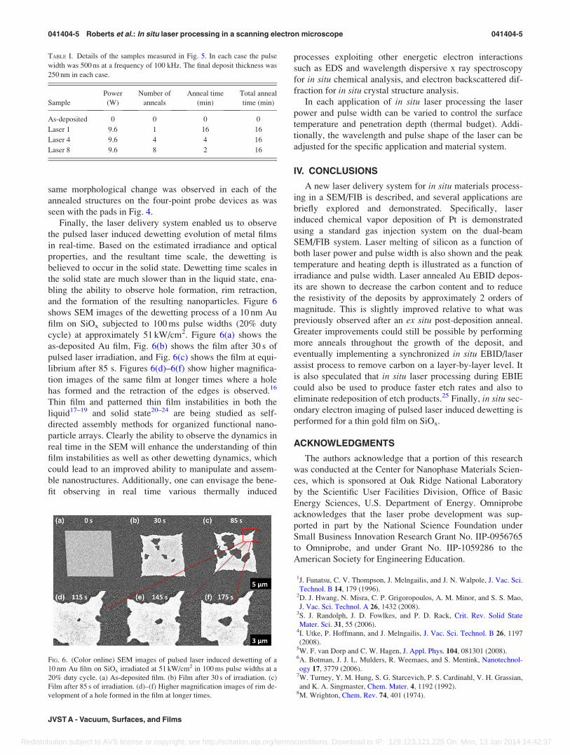
Finally, the laser delivery system enabled us to observe
the pulsed laser induced dewetting evolution of metal films
in real-time. Based on the estimated irradiance and optical
properties, and the resultant time scale, the dewetting is
believed to occur in the solid state. Dewetting time scales in
the solid state are much slower than in the liquid state, ena-
bling the ability to observe hole formation, rim retraction,
and the formation of the resulting nanoparticles. Figure 6
shows SEM images of the dewetting process of a 10 nm Au
film on SiOx subjected to 100 ms pulse widths (20% duty
cycle) at approximately 51 kW/cm2. Figure 6(a) shows the
as-deposited Au film, Fig. 6(b) shows the film after 30 s of
pulsed laser irradiation, and Fig. 6(c) shows the film at equi-
librium after 85 s. Figures 6(d)–6(f) show higher magnifica-
tion images of the same film at longer times where a hole
has formed and the retraction of the edges is observed.16
Thin film and patterned thin film instabilities in both the
liquid17–19 and solid state20–24 are being studied as self-
directed assembly methods for organized functional nano-
particle arrays. Clearly the ability to observe the dynamics in
real time in the SEM will enhance the understanding of thin
film instabilities as well as other dewetting dynamics, which
could lead to an improved ability to manipulate and assem-
ble nanostructures. Additionally, one can envisage the bene-
fit observing in real time various thermally induced
processes exploiting other energetic electron interactions
such as EDS and wavelength dispersive x ray spectroscopy
for in situ chemical analysis, and electron backscattered dif-
fraction for in situ crystal structure analysis.
In each application of in situ laser processing the laser
power and pulse width can be varied to control the surface
temperature and penetration depth (thermal budget). Addi-
tionally, the wavelength and pulse shape of the laser can be
adjusted for the specific application and material system.
IV. CONCLUSIONS
A new laser delivery system for in situ materials process-
ing in a SEM/FIB is described, and several applications are
briefly explored and demonstrated. Specifically, laser
induced chemical vapor deposition of Pt is demonstrated
using a standard gas injection system on the dual-beam
SEM/FIB system. Laser melting of silicon as a function of
both laser power and pulse width is also shown and the peak
temperature and heating depth is illustrated as a function of
irradiance and pulse width. Laser annealed Au EBID depos-
its are shown to decrease the carbon content and to reduce
the resistivity of the deposits by approximately 2 orders of
magnitude. This is slightly improved relative to what was
previously observed after an ex situ post-deposition anneal.
Greater improvements could still be possible by performing
more anneals throughout the growth of the deposit, and
eventually implementing a synchronized in situ EBID/laser
assist process to remove carbon on a layer-by-layer level. It
is also speculated that in situ laser processing during EBIE
could also be used to produce faster etch rates and also to
eliminate redeposition of etch products.25 Finally, in situ sec-
ondary electron imaging of pulsed laser induced dewetting is
performed for a thin gold film on SiOx.
ACKNOWLEDGMENTS
The authors acknowledge that a portion of this research
was conducted at the Center for Nanophase Materials Scien-
ces, which is sponsored at Oak Ridge National Laboratory
by the Scientific User Facilities Division, Office of Basic
Energy Sciences, U.S. Department of Energy. Omniprobe
acknowledges that the laser probe development was sup-
ported in part by the National Science Foundation under
Small Business Innovation Research Grant No. IIP-0956765
to Omniprobe, and under Grant No. IIP-1059286 to the
American Society for Engineering Education.
1J. Funatsu, C. V. Thompson, J. Melngailis, and J. N. Walpole, J. Vac. Sci.
Technol. B 14, 179 (1996).2D. J. Hwang, N. Misra, C. P. Grigoropoulos, A. M. Minor, and S. S. Mao,
J. Vac. Sci. Technol. A 26, 1432 (2008).3S. J. Randolph, J. D. Fowlkes, and P. D. Rack, Crit. Rev. Solid State
Mater. Sci. 31, 55 (2006).4I. Utke, P. Hoffmann, and J. Melngailis, J. Vac. Sci. Technol. B 26, 1197
(2008).5W. F. van Dorp and C. W. Hagen, J. Appl. Phys. 104, 081301 (2008).6A. Botman, J. J. L. Mulders, R. Weemaes, and S. Mentink, Nanotechnol-
ogy 17, 3779 (2006).7W. Turney, Y. M. Hung, S. G. Starcevich, P. S. Cardinahl, V. H. Grassian,
and K. A. Singmaster, Chem. Mater. 4, 1192 (1992).8M. Wrighton, Chem. Rev. 74, 401 (1974).
TABLE I. Details of the samples measured in Fig. 5. In each case the pulse
width was 500 ns at a frequency of 100 kHz. The final deposit thickness was
250 nm in each case.
Sample
Power
(W)
Number of
anneals
Anneal time
(min)
Total anneal
time (min)
As-deposited 0 0 0 0
Laser 1 9.6 1 16 16
Laser 4 9.6 4 4 16
Laser 8 9.6 8 2 16
FIG. 6. (Color online) SEM images of pulsed laser induced dewetting of a
10 nm Au film on SiOx irradiated at 51 kW/cm2 in 100 ms pulse widths at a
20% duty cycle. (a) As-deposited film. (b) Film after 30 s of irradiation. (c)
Film after 85 s of irradiation. (d)–(f) Higher magnification images of rim de-
velopment of a hole formed in the film at longer times.
041404-5 Roberts et al.: In situ laser processing in a scanning electron microscope 041404-5
JVST A - Vacuum, Surfaces, and Films
Redistribution subject to AVS license or copyright; see http://scitation.aip.org/termsconditions. Download to IP: 129.123.121.225 On: Mon, 13 Jan 2014 14:42:37

9I. P. Herman, Chem. Rev. 89, 1323 (1989).10E. Kennedy, G. Byrne, and D. N. Collins, J. Mater. Process. Technol.
155–156, 1855 (2004).11L. Li, Opt. Lasers Eng. 34, 231 (2000).12M. Doubenskaia and I. Smurov, Appl. Surf. Sci. 252, 4472 (2006).13A. Botman, J. J. L. Mulders, and C. W. Hagen, Nanotechnology 20,
372001 (2009).14J. J. L. Mulders, L. M. Belova, and A. Riazanova, Nanotechnology 22,
055302 (2011).15J. D. Wnuk, J. M. Gorham, S. G. Rosenberg, W. F. van Dorp, T. E. Madey,
C. W. Hagen, and D. H. Fairbrother, J. Appl. Phys. 107, 054301 (2010).16See Supplementary Material Document No. http://dx.doi.org/10.1116/
1.4731254 for an in situ scanning electron movie of the dewetting process.17J. Bischof, D. Scherer, S. Herminghaus, and P. Leiderer, Phys. Rev. Lett.
77, 1536 (1996).
18S. Herminghaus, K. Jacobs, K. Mecke, J. Bischof, A. Fery, M. Ibn-Elhaj,
and S. Schlagowski, Science 282, 916 (1998).19Y. Wu, J. D. Fowlkes, N. A. Roberts, J. A. Diez, L. Kondic, A. G. Gonza-
lez, and P. D. Rack, Langmuir 27, 13314 (2011).20A. L. Giermann and C. V. Thompson, J. Appl. Phys. 109, 083520 (2011).21D. Kim, A. L. Giermann, and C. V. Thompson, Appl. Phys. Lett. 95, 1903
(2009).22J. Ye and C. V. Thompson, Phys. Rev. B 82, 3408 (2010).23Y.-J. Oh, C. A. Ross, Y. S. Jung, Y. Wang, and C. V. Thompson, Small 5,
860 (2009).24R. Clearfield, J. G. Railsback, R. C. Pearce, D. K. Hensley, J. D. Fowlkes,
M. Fuentes-Cabrera, M. L. Simpson, P. D. Rack, and A. V. Melechko,
Appl. Phys. Lett. 97, 3101 (2010).25D. Burgess, P. C. Stair, and E. Weitz, J. Vac. Sci. Technol. A 4, 1362
(1985).
041404-6 Roberts et al.: In situ laser processing in a scanning electron microscope 041404-6
J. Vac. Sci. Technol. A, Vol. 30, No. 4, Jul/Aug 2012
Redistribution subject to AVS license or copyright; see http://scitation.aip.org/termsconditions. Download to IP: 129.123.121.225 On: Mon, 13 Jan 2014 14:42:37