
Improved Design and Analysis of Self-Powered Synchronized Switch Interface Circuit for Piezoelectric...
11
1950 IEEE TRANSACTIONS ON INDUSTRIAL ELECTRONICS, VOL. 59, NO. 4, APRIL 2012 Improved Design and Analysis of Self-Powered Synchronized Switch Interface Circuit for Piezoelectric Energy Harvesting Systems Junrui Liang, Member, IEEE, and Wei-Hsin Liao, Senior Member, IEEE Abstract—In piezoelectric energy harvesting (PEH), with the use of the technique named synchronized switch harvesting on inductor (SSHI), the harvesting efficiency can be greatly enhanced. Furthermore, the introduction of its self-powered feature makes this technique more applicable for stand-alone systems. In this paper, a modified circuit and an improved analysis for the self- powered SSHI (SP-SSHI) are proposed. With the modified circuit, direct peak detection and better isolation among different units within the circuit are achieved, both of which result in the further removal on the dissipative components. In the improved analysis, details in the open circuit voltage, switching phase lag, and in- termediate voltages among different phases are discussed, all of which lead to a better understanding on the working principle of SP-SSHI. The total power dissipation from the piezoelectric source is also investigated. It is of concern but has not been considered in the previous literatures. Both analyses and experiments show that, in terms of the harvested power, the higher the excitation level, the closer between SP-SSHI and ideal (externally powered) SSHI; at the same time, the more beneficial the adoption of SP-SSHI treatment in PEH, compared to the standard energy harvesting (SEH) technique. Under the four excitation levels investigated, the SP-SSHI can harvest up to 200% more power than the SEH interface circuit. Index Terms—Energy flow, energy harvesting, interface circuit, piezoelectric, self-powered. I. I NTRODUCTION S TRUCTURED by a certain number of spatially distributed autonomous sensor devices, the wireless sensor networks (WSNs) can be used in military, industrial, and civil appli- cations for monitoring different physical and environmental conditions [1]. Many concerns on energy consumption were addressed due to their nature on wireless connections [2]. Different energy harvesting techniques have been investigated for the purpose to broaden the energy sources, alleviate the dependence on batteries, and hopefully someday make all WSN devices self-powered [3]–[6]. Manuscript received January 29, 2011; revised June 24, 2011; accepted August 15, 2011. Date of publication September 6, 2011; date of current version November 1, 2011. This work was supported by the Research Grants Council of the Hong Kong Special Administrative Region, China under Project CUHK 414809. The authors are with the Department of Mechanical and Automation Engi- neering, The Chinese University of Hong Kong, Shatin, Hong Kong (e-mail: [email protected]; [email protected]). Color versions of one or more of the figures in this paper are available online at http://ieeexplore.ieee.org. Digital Object Identifier 10.1109/TIE.2011.2167116 Piezoelectric energy harvesting (PEH) is one of the promis- ing techniques that can scavenge energy from the ambient vibration sources [4], [7]. With its electromechanical coupling characteristic, a piezoelectric element can generate electricity when strain is produced. Since the deformation in a vibrating structure is alternating, the generated electricity is also alter- nating. On the other hand, the most potential applications for the PEH techniques are WSNs and portable electronics [3]. In these electronic devices, dc power supply is required. Moreover, the storage of electrical energy also requires electrical energy in dc form. Therefore, an interface circuit is needed for ac- dc conversion. The standard energy harvesting (SEH) interface circuit involves only a bridge rectifier for the ac-dc conversion [8]–[10]. The energy harvesting capability can be enhanced by adopting different kinds of switch interface circuits [11]–[13]. In particular, Guyomar et al. proposed a nonlinear technique named synchronized switch harvesting on inductor (SSHI) [14]. It was claimed that, under the same displacement excitation, SSHI can increase the harvested power by several hundred percent, compared to SEH [11], [14]–[16]. The improvement would be more significant for weakly coupled PEH systems [17], [18]. To implement SSHI, a displacement sensor and a controller were usually needed for synchronization and gen- eration of the switching commands [11], [14], [19], [20]. The power consumption of these auxiliary devices could be even higher than the harvestable power [21]. Two solutions can be adopted for implementing SSHI in practical PEH systems. The first is to cut down the power consumption of the auxiliary units (usually integrating them into an integrated circuit), until it could be covered by the harvested power [22]. The second is to build a self-powered SSHI (SP-SSHI) interface circuit, which can automatically switch at voltage peaks without regulated power supply [21], [23]–[25]. In SP-SSHI, the synchronization is carried out based on the information from the peak detectors; at the same time, the switches, which are in fact powered by the piezoelectric source, automatically take actions to invert the piezoelectric voltage once the maxima or minima are attained. Lallart and Guyomar [21] implemented the SP-SSHI inter- face circuit with some discrete electrical components. Based on the experiment, they claimed that their SP-SSHI interface circuit can harvest 1.6 times more power than the SEH one. They have also considered the influence of the voltage drops, which are produced by diodes and transistors in the circuit, over the harvested power. Yet, the influences of other compo- nents, such as the capacitors in the envelope detectors, have 0278-0046/$26.00 © 2011 IEEE
-
Upload
shanghaitech -
Category
Documents
-
view
0 -
download
0
Transcript of Improved Design and Analysis of Self-Powered Synchronized Switch Interface Circuit for Piezoelectric...

1950 IEEE TRANSACTIONS ON INDUSTRIAL ELECTRONICS, VOL. 59, NO. 4, APRIL 2012
Improved Design and Analysis of Self-PoweredSynchronized Switch Interface Circuit forPiezoelectric Energy Harvesting Systems
Junrui Liang, Member, IEEE, and Wei-Hsin Liao, Senior Member, IEEE
Abstract—In piezoelectric energy harvesting (PEH), with theuse of the technique named synchronized switch harvesting oninductor (SSHI), the harvesting efficiency can be greatly enhanced.Furthermore, the introduction of its self-powered feature makesthis technique more applicable for stand-alone systems. In thispaper, a modified circuit and an improved analysis for the self-powered SSHI (SP-SSHI) are proposed. With the modified circuit,direct peak detection and better isolation among different unitswithin the circuit are achieved, both of which result in the furtherremoval on the dissipative components. In the improved analysis,details in the open circuit voltage, switching phase lag, and in-termediate voltages among different phases are discussed, all ofwhich lead to a better understanding on the working principle ofSP-SSHI. The total power dissipation from the piezoelectric sourceis also investigated. It is of concern but has not been considered inthe previous literatures. Both analyses and experiments show that,in terms of the harvested power, the higher the excitation level,the closer between SP-SSHI and ideal (externally powered) SSHI;at the same time, the more beneficial the adoption of SP-SSHItreatment in PEH, compared to the standard energy harvesting(SEH) technique. Under the four excitation levels investigated,the SP-SSHI can harvest up to 200% more power than the SEHinterface circuit.
Index Terms—Energy flow, energy harvesting, interface circuit,piezoelectric, self-powered.
I. INTRODUCTION
S TRUCTURED by a certain number of spatially distributedautonomous sensor devices, the wireless sensor networks
(WSNs) can be used in military, industrial, and civil appli-cations for monitoring different physical and environmentalconditions [1]. Many concerns on energy consumption wereaddressed due to their nature on wireless connections [2].Different energy harvesting techniques have been investigatedfor the purpose to broaden the energy sources, alleviate thedependence on batteries, and hopefully someday make all WSNdevices self-powered [3]–[6].
Manuscript received January 29, 2011; revised June 24, 2011; acceptedAugust 15, 2011. Date of publication September 6, 2011; date of current versionNovember 1, 2011. This work was supported by the Research Grants Councilof the Hong Kong Special Administrative Region, China under Project CUHK414809.
The authors are with the Department of Mechanical and Automation Engi-neering, The Chinese University of Hong Kong, Shatin, Hong Kong (e-mail:[email protected]; [email protected]).
Color versions of one or more of the figures in this paper are available onlineat http://ieeexplore.ieee.org.
Digital Object Identifier 10.1109/TIE.2011.2167116
Piezoelectric energy harvesting (PEH) is one of the promis-ing techniques that can scavenge energy from the ambientvibration sources [4], [7]. With its electromechanical couplingcharacteristic, a piezoelectric element can generate electricitywhen strain is produced. Since the deformation in a vibratingstructure is alternating, the generated electricity is also alter-nating. On the other hand, the most potential applications forthe PEH techniques are WSNs and portable electronics [3]. Inthese electronic devices, dc power supply is required. Moreover,the storage of electrical energy also requires electrical energyin dc form. Therefore, an interface circuit is needed for ac-dc conversion. The standard energy harvesting (SEH) interfacecircuit involves only a bridge rectifier for the ac-dc conversion[8]–[10]. The energy harvesting capability can be enhanced byadopting different kinds of switch interface circuits [11]–[13].In particular, Guyomar et al. proposed a nonlinear techniquenamed synchronized switch harvesting on inductor (SSHI) [14].It was claimed that, under the same displacement excitation,SSHI can increase the harvested power by several hundredpercent, compared to SEH [11], [14]–[16]. The improvementwould be more significant for weakly coupled PEH systems[17], [18]. To implement SSHI, a displacement sensor and acontroller were usually needed for synchronization and gen-eration of the switching commands [11], [14], [19], [20]. Thepower consumption of these auxiliary devices could be evenhigher than the harvestable power [21]. Two solutions can beadopted for implementing SSHI in practical PEH systems. Thefirst is to cut down the power consumption of the auxiliaryunits (usually integrating them into an integrated circuit), untilit could be covered by the harvested power [22]. The second isto build a self-powered SSHI (SP-SSHI) interface circuit, whichcan automatically switch at voltage peaks without regulatedpower supply [21], [23]–[25]. In SP-SSHI, the synchronizationis carried out based on the information from the peak detectors;at the same time, the switches, which are in fact powered bythe piezoelectric source, automatically take actions to invert thepiezoelectric voltage once the maxima or minima are attained.
Lallart and Guyomar [21] implemented the SP-SSHI inter-face circuit with some discrete electrical components. Basedon the experiment, they claimed that their SP-SSHI interfacecircuit can harvest 1.6 times more power than the SEH one.They have also considered the influence of the voltage drops,which are produced by diodes and transistors in the circuit,over the harvested power. Yet, the influences of other compo-nents, such as the capacitors in the envelope detectors, have
0278-0046/$26.00 © 2011 IEEE

LIANG AND LIAO: IMPROVED DESIGN AND ANALYSIS OF SELF-POWERED SYNCHRONIZED SWITCH INTERFACE CIRCUIT 1951
Fig. 1. Equivalent circuit of a PEH device.
not been pointed out. In addition, two important parameters,i.e., the switching delay phase ϕ and inversion factor γ, wereregarded as constants. However, in fact, these two parametersare constants only when the open circuit voltage VOC (relatedto displacement magnitude) and storage voltage VDC (voltageacross the storage device) are constants. A more completeanalysis should take these into account, for comparing theenergy harvesting efficiencies under different VOC and VDC .Instead of using transistors to switch the inductor shunt, Qiuet al. [24] used two silicon controlled rectifiers to constructtheir SP-SSHI interface circuit; yet, analysis on the principleand performance details about the proposed circuit was lacked.
In the aforementioned literatures, the energy dissipation inthe SP-SSHI circuit and the performance difference betweenthe SP-SSHI and ideal (externally powered) SSHI interfacecircuits were not shown. Without considering these issues,the cost for implementing the self-powered switching actionscannot be specified. Moreover, in either literature, only theperformance of the SP-SSHI device under a specified vibrationmagnitude was investigated. Given that, in SP-SSHI, a partof the harvested power must be consumed to carry out theswitching actions, it would be too strong to conclude thatSP-SSHI always outperforms SEH.
In this paper, a modified circuit topology for SP-SSHI is pro-posed. The circuit is built with discrete electrical components.With the adoption of a complementary topology, the peak detec-tion units can be separated from the switching inductive shunt;therefore, better isolation can be achieved. An improved analy-sis is also provided considering the aforementioned concernsabout SP-SSHI. Section II introduces the working principles ofPEH as well as the SSHI interface circuit. Section III proposesthe modified circuit topology for SP-SSHI. Section IV providesan improved analysis on SP-SSHI. Section V compares anddiscusses the experimental and analytical results. Section VIconcludes the paper.
II. PRINCIPLES
A. Piezoelectric Energy Harvesting
Given a typical PEH device, e.g., a piezoelectric cantileverwith harvesting interface circuit and energy storage, the piezo-electric structure can be modeled as an equivalent currentsource ieq in parallel with the piezoelectric clamped capaci-tance Cp and the internal leakage resistance Rp, as shown inFig. 1. The current source ieq is proportional to the vibrationvelocity x with the relation of
ieq(t) = αex(t) (1)
whereαe is the force-voltage factor of the piezoelectric structure.
Fig. 2. Equivalent circuits of two SSHI treatments. (a) P-SSHI. (b) S-SSHI.
Different interface circuits could be designed for differentobjectives; yet, in terms of energy flow, they all extract energyfrom the vibrating mechanical structure. For the purpose of vi-bration suppression, usually the extracted energy is dissipated,while for energy harvesting, a portion of the extracted energyis reclaimed and stored in electrical form for the subsequentusage. As shown in Fig. 1, for a PEH device, the interface cir-cuit provides power conditioning, and then the energy storagedevice stores the harvested energy, while a part of the harvestedenergy is used to power the dc load.
B. SSHI Interface Circuit
In a vibrating piezoelectric device, since the induced voltageacross the piezoelectric capacitance is alternating, the mostconventional way to turn an ac voltage into dc is to use a bridgerectifier for rectification and then a capacitor for filtering. Thecombination of bridge rectifier and filter capacitor forms thestandard interface circuit that can be used for energy harvesting,i.e., SEH. Ottman et al. [8], [9] discussed the optimization of theSEH technique. Yet, using SEH cannot ensure that the energy isalways flowing from the mechanical part to the electrical part.During a certain interval in each cycle, energy returns from theelectrical part to the mechanical part. It was called the energyreturn phenomenon [16].
The SSHI treatment overcomes this problem by adding aninductive switch path, which is composed of a switching com-ponent sw and an inductor Li to the SEH circuit. This path canbe connected in parallel to the bridge rectifier to form a parallelSSHI (P-SSHI) circuit [Fig. 2(a)], or in series to form a seriesSSHI (S-SSHI) circuit [Fig. 2(b)] [11]. Regardless of P-SSHI orS-SSHI, the switch switches on to form the series loop once thedisplacement x reaches its extreme values, and then switchesoff after half of an resistance inductance capacitance (RLC)cycle, as shown in Fig. 3(c), so as to allow a natural inversionto vp, the voltage across the piezoelectric element. Since theperiod of the RLC circuit 2π
√LiCp is usually selected to be
much smaller than the vibration period that equals to 2π/ω, thevoltage inversion is regarded to be finished in an instant. Onthe other hand, the vibration period is much smaller than thetime constant RpCp, the influence of Rp during the switching-on interval is negligible.

1952 IEEE TRANSACTIONS ON INDUSTRIAL ELECTRONICS, VOL. 59, NO. 4, APRIL 2012
Fig. 3. Typical waveforms of two SSHI treatments. (a) P-SSHI. (b) S-SSHI.(c) Inversion of vp at the instant of extreme displacements.
The voltage relation before and after the switching action inSSHI is described by the following equation:
Voff − Vref = γ(Von − Vref ) (2)
where Von and Voff are the voltages before and after theinversion, respectively; Vref is the reference voltage; γ is theinversion factor that is defined as1
γ = −e−π/(2Q). (3)
Q is the quality factor of the sw − Li − Cp loop. In P-SSHI,Vref equals to zero; in S-SSHI, Vref equals to the rectifiedvoltage Vrect, which is the sum of the voltage drop of a practicalrectifier and the storage voltage VDC , i.e., the voltage acrossthe filter capacitance Crect.2 Typical waveforms in P-SSHI andS-SSHI as well as the zoom-in view of one of their switchingintervals are shown in Fig. 3. Since ieq is proportional tothe velocity x, these switching actions make sure that vp andieq have the same sign; therefore, their product, the powerinput from the mechanical part to the electrical part, is alwayspositive.
To implement SSHI, additional units for displacement peakdetection and switch control are required. In most of theresearches, these functions were realized with displacementsensors and digital controllers [11], [14], [19], all of which needexternal power to run. In [21], all these units were replacedby an SP-SSHI circuit.3 It makes use of the piezoelectricelement itself as a displacement sensor and generates switchingcommands with transistors accordingly. The introduction ofthis SP-SSHI allows the SSHI technique to be more compactand independent of the external power and therefore opensa more promising future to the SSHI technique. Yet, someconcerns about the SP-SSHI were still not addressed in [21].For example, is there any constraint or applicable range forthis treatment? Does the SP-SSHI always outperform SEH? Inthe following sections, the SP-SSHI treatment will be furtherinvestigated concerning these issues.
1The definition on voltage inversion factor in this paper is different from thatin [21]. The sign information is also included in this definition.
2Since Crect is usually selected to be much larger than Cp, VDC is regardedconstant during each vibration cycle.
3More exactly, it is a self-powered S-SSHI device in [21].
III. CIRCUIT
The essence of the SP-SSHI technique proposed in [21],[23], [24] is the electronic breaker. Without providing externalpower, it can automatically perform switching actions oncethe voltage across the switch reaches its maxima. Since onebreaker can only allow the current flow in one direction, re-placing the switch in either Fig. 2(a) and (b) with two of suchbreakers (one as maximum breaker and the other, which wasinversely connected, as minimum breaker), the SP-SSHI can beachieved. The breaker consists of three parts: envelope detector,comparator, and switch. In the design presented by Lallart andGuyomar [21], the envelope detectors were in series with theclamped capacitance Cp and inductor Li. The detected voltagein fact was not vp, but the voltage sum of vp and the voltageacross Li. Even Li is connected to Cp for a very short intervalin every cycle, the hard switching-off action introduces highfrequency components to Li. The local maxima or minimaproduced by these high frequency components may inducemisjudgment to the other breaker. Therefore, both the envelopedetector and comparator parts should be carefully isolated fromthe switching path. For the breaker introduced in [21], [24],several resistors were connected for the isolation purpose. Yet,the principle and design guideline were not clearly provided.
Taking these envelope detection and isolation issues into con-sideration, in our self-powered design, we use complementarytransistors topology to achieve both direct envelope detectionfor vp and reduction on the interference among different partsin the breakers. With this reformation, all the isolating resistors,which are bound to consume some energy, can be removed.The modified SP-SSHI circuit for S-SSHI is shown in Fig. 4.4
We obtain its waveforms (Fig. 5), as well as the zoom-in viewaround one of the processes of switching on maxima (Fig. 6)with the PSpice simulation. The component values and modelsused in simulation are listed in Table I. vC1 and vC2 in Fig. 5denote the voltages across C1 and C2; iD5, iD6, iC1, and iC2 inFig. 6 denote the currents flowing through D5, D6, C1, and C2,respectively.
Accompanying with the vibration, switching actions takeplace when vp reaches its maximum or minimum in each cycle.Different from the ordinary SSHI interface, which has onlyone voltage inversion in each switching action, in the SP-SSHIcircuit, two voltage inversions and one charge neutralization areexperienced accompanying with each switching action, whichcan be figured out from the voltage and current waveformswithin the switching intervals, as shown in Fig. 6. Combiningwith the natural charging phase toward maximum or minimum,we can divide half of a vibration cycle into four phases.
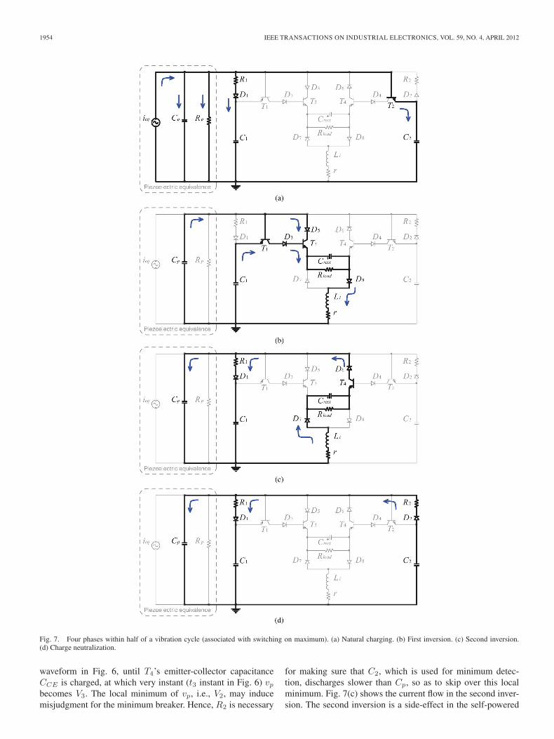
Take the half vibration cycle associated with switching onmaximum for discussion. Fig. 7 shows the detailed workingprinciple of the four phases. For the switching on maximum,R1, D1, and C1 form an envelope detector. T1 acts as acomparator while T3 acts as the electronic switch.
4The self-powered interface circuit for P-SSHI can be modified from that forS-SSHI. In this paper, the analysis and experiment focus on the S-SSHI case forshowing the principle and insights about the self-powered switching interfacecircuit.

LIANG AND LIAO: IMPROVED DESIGN AND ANALYSIS OF SELF-POWERED SYNCHRONIZED SWITCH INTERFACE CIRCUIT 1953
Fig. 4. Modified SP-SSHI interface circuit.
Fig. 5. Simulation waveforms in the modified SP-SSHI.
Fig. 6. Voltage and current waveforms in the process of switching on maximum.
Natural Charging: The current flow in the phase of naturalcharging toward the maximum value of vp is shown in Fig. 7(a).In this phase, only the paths of the two envelop detectors in
TABLE ICOMPONENT MODELS OR VALUES
the interface circuit conduct; all transistors are cut off. Positiveequivalent current ieq charges Cp, C1, and C2, so that vp, vC1,and vC2 increase simultaneously, as shown in Fig. 5.
First Inversion: When vp reaches its maximum Vmax, thevoltage across C1 is Vmax − VD, where VD denotes the for-ward voltage drop of a diode. Then, vp begins to drop. Whenthe decrease reaches VD + VBE ,5 i.e., vp = V1 (t1 instant inFig. 6), the transistor T1 conducts. C1 begins to dischargethrough T1(ec), D3, T3(be), Crect, D8, Li, and r (as observedfrom the iC1 waveform in Fig. 6), consequently makes T3
conduct.6 The conduction of T3 switches on the inductive paththat consists of D5, T3(ce), Crect, D8, Li, and r, producing ashortcut to the charge in Cp. Cp starts a quick discharge fromthe voltage V1 through the inductive path (as observed from theiD5 waveform in Fig. 6), until vp reaches its local minimum (t2instant in Fig. 6). The current flow in the first inversion is shownin Fig. 7(b).
Second Inversion: The current through Li now tends toreverse its flowing direction, but the T3(ce) path is immediatelyblocked by the reverse D5. As observed from Fig. 6, iD5
maintains at zero after the t2 instant. Yet, the path consistingof D7, Crect, T4(ce), and D6 is still available. Because evenT4 is cut off, there is a small parasitic capacitance across itsemitter and collector, which is uncharged. The reverse currentflows through this path, as it can be observed from the iD6
5VBE denotes the transistor base-emitter threshold voltage.6The component r in Fig. 4 represents the total equivalent series resistance
of the non-ideal switching path. It is composed of the parasitic resistances ofthe inductor, diodes, and transistors.
1954 IEEE TRANSACTIONS ON INDUSTRIAL ELECTRONICS, VOL. 59, NO. 4, APRIL 2012
Fig. 7. Four phases within half of a vibration cycle (associated with switching on maximum). (a) Natural charging. (b) First inversion. (c) Second inversion.(d) Charge neutralization.
waveform in Fig. 6, until T4’s emitter-collector capacitanceCCE is charged, at which very instant (t3 instant in Fig. 6) vp
becomes V3. The local minimum of vp, i.e., V2, may inducemisjudgment for the minimum breaker. Hence, R2 is necessary
for making sure that C2, which is used for minimum detec-tion, discharges slower than Cp, so as to skip over this localminimum. Fig. 7(c) shows the current flow in the second inver-sion. The second inversion is a side-effect in the self-powered

LIANG AND LIAO: IMPROVED DESIGN AND ANALYSIS OF SELF-POWERED SYNCHRONIZED SWITCH INTERFACE CIRCUIT 1955
interface to counteract the energy conversion enhancement.This side-effect can be limited by selecting transistors withsmall emitter-collector capacitor capacitance CCE as theswitches. However, it cannot be completely got rid of, sincethe parasitic capacitance CCE cannot be totally removed froma practical transistor.
Charge Neutralization: After t3, both T3 and T4 are cut off;however, C2 still has not finished its discharging, the rest of thecharge in C2 will flow into Cp and C1 until they are the same involtage. The discharge of C2 is reflected by the iC2 waveformshown in Fig. 6. It stops when iC2 approaches zero (t4 instantin Fig. 6). This charge neutralization again increases vp a littlebit to V4 before vp enters the following half cycle of minimumdetection. The actual discharge of C2 starts from t1, as observedfrom the iC2 waveform in Fig. 6; yet, to simplify the analysis,the charge neutralization is assumed to be an independent phaseother than the other three phases. The current flow in this chargeneutralization phase is shown in Fig. 7(d).
Switching on minimum makes use of the counterparts inthe circuit, and its principle is similar to that of switchingon maximum. Because of the complementary topology, forthe switching on minimum, the four intermediate voltages are−V1, −V2, −V3, and −V4, respectively. The analysis on thefour phases within half of a vibration cycle helps understandthe working principle of the SP-SSHI interface circuit andalso provides guidance for the component selection. From thevoltage waveforms of vp, vC1, and vC2 shown in Fig. 5, C1
and C2 in the envelop detectors are approximately connectedin parallel to Cp. They affect the original system and decreasethe magnitude of the open circuit voltage. This influence can bereduced by selecting small C1 and C2; yet, they cannot be toosmall, because the stored charge in these two capacitors shouldbe enough to drive the corresponding transistors for carryingout switching actions. To determine the values of these two ca-pacitors, some trial-and-error experiments should be involved,and the value might be different according to the selectedtransistors. On the other hand, the values of C1 and R1 (or C2
and R2, respectively) should satisfy the following criterion:
2π√
LiCp < RedCed π
ω(4)
where ω is the frequency of the mechanical vibration. Becausethe capacitors C1 and C2 in the envelope detectors are selectedto be the same value, they are denoted as Ced in (4); similarly,R1 and R2 are denoted as Red. The first inequality ensuresthat the charge neutralization finishes later than the twovoltage inversions, so as to avoid the misjudgment on localminima or maxima. The second inequality implies that thecharge neutralization should use much less time than half ofa vibration cycle, so that the influence induced by insertingenvelop detectors can be minimized.
IV. ANALYSIS
In Section III, the working principle of the modifiedSP-SSHI circuit has been introduced. Based on this, detailedand quantitative analysis is provided in this section.
A. Open Circuit Voltage
The effect of the two capacitors C1 and C2 in the envelopdetectors was not taken into account in [21]. Within one vibra-tion cycle, the energy that is flowed into these two capacitorswill return to the mechanical part rather than being stored inthemselves nor used to power the dc load. Therefore, C1 andC2 can be equivalently regarded as two capacitors connectedin parallel to Cp. This approximation is validated from Fig. 5,since both vC1 and vC2 are very close to vp. Given the harmonicdisplacement excitation as
x(t) = X sin(ωt) (5)
where X is the magnitude of the vibration displacement. With(1), the equivalent current source should be
ieq(t) = αeXω cos(ωt). (6)
With the parallel connections of Cp, Rp, C1, and C2, at opencircuit condition, vp becomes
vp,oc(t) = VOC sin(ωt + θ) (7)
where
VOC =αeXωRp√
1 + ω2R2p(Cp + 2Ced)2
(8)
θ = tan−1
[1
ωRp(Cp + 2Ced)
]. (9)
VOC is the open circuit voltage, representing the magnitudeof vp; θ is the phase difference between the maximum vp,oc
and the zero crossing point (from positive to negative) ofieq, as shown in Fig. 5. Without shunt circuit connected,the original open circuit voltage of the piezoelectric struc-ture is
VOC,org =αeXωRp√1 + ω2R2
pC2p
. (10)
Therefore, (8) implies that the open circuit voltage inSP-SSHI will be slightly reduced from VOC,org under the sameexcitation.
In addition, to effectively drive the switches, there is aconstraint for VOC , which is set by the forward voltage drops ofdiodes and transistors in the circuit. To figure out the constraint,suppose no switching action is performed before the connectionof the circuit. Once it is connected, the first switching actionmay start after vp attains, for example, its maximum, i.e., VOC ,and then drops to VOC − VD − VBE . At this time, T1 willconduct only when vC1 is larger than the voltage drop producedby T1(ec), D3, T3(be), Crect, and D8 in series, and T3 willconduct only when vp is larger than the voltage drop produced

1956 IEEE TRANSACTIONS ON INDUSTRIAL ELECTRONICS, VOL. 59, NO. 4, APRIL 2012
by D5, T3(ce), Crect, and D8 in series. Both yield the sameconstraint for VOC as
VOC > VCE(sat) + 3VD + VBE + VDC (11)
where VCE(sat) is the collector-emitter saturation voltage of thecorresponding transistors.
On the other hand, given a VDC satisfying (11), we can obtainthe maximum attainable VDC in energy harvesting from (11), asfollows:
VDC,max = VOC − VCE(sat) − 3VD − VBE . (12)
B. Switching Phase Lag
From the principle of SSHI [11], the switching actions shouldbe taken at the right instants when vp attains its extremevalues, i.e., Vmax or Vmin in Fig. 5. In SP-SSHI, however, toswitch at the very instants would be impossible; due to thevoltage drops of diodes and transistors in the envelope detectorsand comparators, there is a phase lag between the instants ofswitching action start and the maximum (or minimum) vp. Thisphase lag is shown as ψ in Fig. 5 and calculated with thefollowing relation:
ψ = cos−1
(1 − VD + VBE
VOC
). (13)
Combining (9) and (13), the phase difference between theinstants of maximum vp and maximum displacement (alsoieq = 0) can be obtained as
ϕ = ψ − θ. (14)
This phase difference ϕ was regarded as constant in [21].Nevertheless, given the above relations, ϕ in fact changes withVOC . Considering the constraint on VOC given in (12), therange of ϕ can be obtained as
− θ<ϕ<cos−1
[VCE(sat)+2VD+VDC
VCE(sat)+3VD+VBE +VDC
]−θ. (15)
The lower limit corresponds to infinite VOC ; the upper onecorresponds to the minimum harvestable VOC .
C. Intermediate Voltages among Four Phases
In the externally powered SSHI, there are only two phasesin a half vibration cycle, i.e., natural charging and voltageinversion. The two intermediate voltages can be calculated ac-cording to the charging and discharging processes in these twophases. In SP-SSHI, owing to the interactions among differentparts in the self-powered switching circuit, more phases aredistinguished for better analysis about the circuit behavior. Fourworking phases were introduced in Section III. As shown inFig. 6, the four phases are linked by four intermediate voltagesfrom V1 to V4.
In the switching on maximum, if V1 > Vref1, where
Vref1 = VCE(sat) + 2VD + VDC (16)
is the first reference voltage, vp will experience the first in-version. For the first inversion, i.e., from V1 to V2, Cp + C1,Li, and r form an RLC loop for discharging, with the qualityfactor of
Q1 =1r
√Li
Cp + Ced. (17)
The relation between V2 and V1 can be obtained as
V2 − Vref1 = γ1(V1 − Vref1) (18)
where
γ1 =−e−π/(2Q1), V1 > Vref1;1, others
(19)
is the inversion factor of the corresponding RLC loop, whosequality factor is Q1.
After the first inversion, if V2 < Vref2, where
Vref2 = −2VD − VDC (20)
is the second reference voltage, vp will experience one moreinversion. For the second inversion, i.e., from V2 to V3, Cp
in series with CCE , Li, and r form another RLC loop fordischarging, with the quality factor of
Q2 =1r
√Li(Cp + CCE)
CpCCE. (21)
The relation between V3 and V2 can be obtained as
V3 −Cp
CCE(V2 − V3) − Vref2 = γ2(V2 − Vref2) (22)
where
γ2 =−e−π/(2Q2), V2 < Vref2;1, others
(23)
is the inversion factor of the corresponding RLC loop, whosequality factor is Q2.
Assuming that the discharge of C2 starts after the twoinversion of vp, the charge neutralization is regarded as anindependent phase. In the charge neutralization, the total chargein Cp, C1, and C2 is unchanged. Considering their originalvoltages, V4 is related to V1, V2, and V3 with the followingequation:
(Cp + 2Ced)V4 = Ced(V1 + V2) + CpV3. (24)
After the charge neutralization, the natural charging starts.It lasts for half of a vibration cycle, until vp reaches −V1, the

LIANG AND LIAO: IMPROVED DESIGN AND ANALYSIS OF SELF-POWERED SYNCHRONIZED SWITCH INTERFACE CIRCUIT 1957
start voltage of the switching on minimum. The voltage relationcorresponding to this phase can be obtained as follows:
−V1 = V4 +1
Cp + 2Ced
3π/2+ϕω∫
π/2+ϕω
[ieq(t) −
vp(t)Rp
]dt. (25)
Since the durations of the two inversions and the charge neu-tralization are much shorter than a half vibration cycle, the vp
waveform can be approximated by splitting the vp,oc one at theswitching instants and then moving the adjacent parts againsteach other to some extent, i.e.,
vp(t) =
vp,oc(t) + V1−V42 ,
(n − 1
2
)π + ϕ < ωt
≤(n + 1
2
)π + ϕ,
vp,oc(t) − V1−V42 ,
(n + 1
2
)π + ϕ < ωt
≤(n + 3
2
)π + ϕ,
n ∈Z. (26)
Substituting the approximated vp in (26) into (25), and givenω(Cp + 2Ced)Rp 1, we can have
−V1 = V4 − 2VOC cos ϕ +4VOC sinψ + π(V1 − V4)
2ω(Cp + 2Ced)Rp. (27)
Equation (27) provides the relations between V1 and V4. Com-bining the linear equations of (18), (22), (24), and (27), the fourintermediate voltages from V1 to V4 can be solved out, in termsof VOC and VDC .
D. Harvested and Dissipated Powers
The energy flow within the PEH system is of concern for theoverall evaluation on the performance of the harvesting systems[20]. Based on the above analyses about the influences of self-powered implementation on the open circuit voltage, switchingphase lag, and intermediate voltages, the harvested power aswell as the power dissipated during the harvesting process inSP-SSHI can be calculated as follows:
Ph,SP−SSHI
= 2f0VDC [Cp(V1 + V3 − 2V2) + Ced(V1 − V2)] , (28)Pd,SP−SSHI
= f0
(Cp + 2Ced)
[(V1 − Vref1)2 − (V4 − Vref1)2
]+ 2(VCE(sat) + 2VD)
[Cp(V1 + V3 − 2V2)
+ Ced(V1 − V2)]
+1
ωRp
[πV 2
OC − 4VOC(V1 − V4) sin ψ
+π(V1 − V4)2
2
](29)
where f0 = ω/(2π) is the vibration frequency in Hz. The threeitems in (29) estimate the power dissipations produced by thenon-ideal voltage inversions, components’ voltage drops, and
Fig. 8. Experimental setup.
the internal loss within the piezoelectric element. It should benoted that the harvested power here is the net harvested power.The sensing, comparing, and switching units in the circuitin fact are powered by the piezoelectric source. The powerconsumed in these units has already been included in the totaldissipated power given in (29).
Moreover, the SEH and externally powered SSHI arealso employed for the evaluation on the performance of theSP-SSHI. The harvested and dissipated powers in SEH are
Ph,SEH = 4f0CpVDC(VOC,org − VDC − 2VD) (30)
Pd,SEH = 8f0CpVD(VOC,org − VDC − 2VD). (31)
Considering the influence of the internal loss within the piezo-electric element, the expressions on the harvested and dissi-pated powers in externally powered S-SSHI were provided in[26].7
V. RESULTS
Experiments are carried out to evaluate the performance ofpractical SP-SSHI. The experimental setup is shown in Fig. 8.It is built up with a piezoelectric cantilever and the modifiedSP-SSHI interface circuit.
The main mechanical structure is an aluminum cantileverwhose fixed end is fixed on the vibration-free table while thefree end is driven by an electromagnetic driver. A piezoceramicpatch of 49 mm × 24 mm × 0.508 mm (T120-A4E-602, PiezoSystem, Inc.) is bonded near the fixed end where the largeststrain happens along the cantilever. A permanent magnet isattached at the free end of the cantilever, so as to achieve thecoupling with the electromagnetic driver, and it also acts as aproof mass to lower the vibration frequency and increase thedisplacement of the free end. A function generator (33120A,Agilent Co.), following by a power amplifier (2706, B & KCo.), provides a 30 Hz sinusoidal excitation to the electro-magnetic coil. To provide constant displacement excitation, aninductive displacement sensor (JCW-24SR, CNHF Co.), whichis not shown in Fig. 8, is used to measure the displacement
7In the externally powered SSHI, the sensing and switching con-trol units do not affect VOC , and there is no switching phase delay;however, the voltage drop of bridge rectifier was considered nonzeroin [26].

1958 IEEE TRANSACTIONS ON INDUSTRIAL ELECTRONICS, VOL. 59, NO. 4, APRIL 2012
TABLE IIOTHER CIRCUIT PARAMETERS
Fig. 9. Sensitivities of the harvested power. (a) Over the capacitance inthe envelop detectors, i.e., Ced (Red = 200 kΩ, VOC,org = 25 V, VDC =10 V). (b) over the resistance in the envelop detectors, i.e., Red (Ced = 2 nF,VOC,org = 25 V, VDC = 10 V).
of the cantilever for adjustment under different situations. Thecircuit component models and values in the experiment arelisted in Table I. Other circuit parameters are given in Table II.
As for the selection of components in the self-poweredswitching interface circuit, the models of the diodes and tran-sistors are not specific; other than these two components, thevalues of the resistors and capacitors in the envelop detectors,i.e., Ced and Red, need to be determined according to theinequality given in (4). Fig. 9 shows the sensitivities of the har-vested power over the variations of Ced and Red, respectively.The simulation results for the Ced case match the theory well,except when the Ced is too small to provide enough currentfor driving the transistors. The effect of Red is not involved inthe theoretical estimation. However, given Ced is fixed at 2 nF,based on the relation provided in (4), the range of Red isobtained from 125 kΩ to 493 kΩ. The simulation results shownin Fig. 9(b) agree with the theory within this range. Belowthe lower bound, improper switching actions are observed atlocal maxima or minima; above the upper bound, the largerRed, the larger the discrepancy on estimation. In general, withthe premise that the SP-SSHI circuit can properly function, thevalues of Ced should be selected as small as possible, so that theinfluence caused by the envelop detectors can be minimized;at the same time, the value of Red should be determinedbased on (4).
The harvested and dissipated powers under four differentexcitation levels are investigated. Without the self-poweredcircuit connected, the four excitation levels induce 5, 8, 12, and25 volt open circuit voltages VOC,org across the piezoelectricelement, respectively. Under those four excitation levels, theharvested power is measured as a function of the storage voltageVDC . Resistors with different resistance values are connected asloads one by one. With the corresponding measured dc voltageacross each resistor, the harvested power under different VDC
can be obtained. The experimental results of Ph,SP−SSHI ,Pd,SP−SSHI , and Ph,SEH under the four excitation levels, to-gether with the analytical results on the harvested and dissipatedpowers in the three interface circuits of SP-SSHI, SEH, andideal SSHI, are shown in Fig. 10 for comparison. From the foursubfigures in Fig. 10, both of the analytical and experimentalresults show good agreement with each other.
Comparing SP-SSHI to ideal SSHI, the higher the exci-tation level, the closer between the corresponding curves,i.e., Ph,SP−SSHI versus Ph,SSHI and Pd,SP−SSHI versusPd,SSHI , which means that the SP-SSHI approaches the idealSSHI, in terms of both harvested and dissipated powers. Sincethe total electrical extracted power is composed of harvestedand dissipated portions [20], the harvested percentages withinthe extracted power under different conditions are shown inFig. 11, where VDC is the nondimensional storage voltagenormalized to VOC,org. From these figures, the maximum har-vested percentage in the SP-SSHI gets higher as the excitationlevel increases. In addition, under the same excitation level, theharvested percentage in the SP-SSHI might be higher than thatin the ideal SSHI case when VDC is small, but in terms of themaximum value, the harvested percentage in the SP-SSHI isless than that in the ideal SSHI.
Comparing the SP-SSHI to SEH, the largest increase in themaximum harvested power is about 200%, as observed fromFig. 10(d). However, meanwhile it should be noted that, unlikethe ideal SSHI, whose harvested power has a constant magni-fication toward that in SEH, the superiority of SP-SSHI overSEH varies. The improvement is more significant under highexcitation level; under low excitation, it may lose its benefit.For example, as shown in Fig. 10(a), when VOC,org = 5 V,the maximum harvested power in the SP-SSHI is smaller thanthat in the SEH. On the other hand, for the SP-SSHI underthis excitation, the experimental result is even smaller than thetheoretical prediction. This is because the transistor in the realcircuit cannot be fully turned on and off in time under thislow level excitation. Fig. 12 shows the theoretical maximumharvested power as functions of the original open circuit voltagein the SP-SSHI and SEH, respectively. The critical open circuitvoltage is 5.84 V for the experimental setup used in this paper.Only when the excitation level is above this critical point, theSP-SSHI can harvest more power than the SEH. On the otherhand, as observed from Fig. 11, the harvested percentage inthe SEH is always larger than those in the SP-SSHI and theideal SSHI regardless of the excitation level VOC,org and thestorage voltage VDC . In general, rather than claiming thatthe SP-SSHI always outperforms the SEH, it should be carefulto examine the broader range of operation when implementingthis SP-SSHI interface circuit.
VI. CONCLUSION
The introduction of the self-powered version of the SSHIdid open a promising treatment for PEH with switching tech-nique. Nevertheless, issues still lie in further improvements onboth circuit and accurate modeling. We proposed a modifiedcircuit for the SP-SSHI. Compared to the circuitry proposed in[21], the modified circuit not only minimizes the interference

LIANG AND LIAO: IMPROVED DESIGN AND ANALYSIS OF SELF-POWERED SYNCHRONIZED SWITCH INTERFACE CIRCUIT 1959
Fig. 10. Harvested and dissipated powers under different excitation levels. (a) VOC,org = 5.0 V. (b) 8.0 V. (c) 12.0 V. (d) 25.0 V.
Fig. 11. Harvested percentage within the extracted power. (a) VOC,org = 5.0 V. (b) 8.0 V. (c) 12.0 V. (d) 25.0 V.
Fig. 12. Maximum harvested power in SP-SSHI and SEH under differentexcitation levels.
among different units in the circuit, so as can enhance theswitching performance, but also results in the removal of someresistive components, so as to further diminish the energydissipation within the switching processes. Improved analysiswas performed considering three aspects, including the opencircuit voltage, switching phase lag, and intermediate voltagesamong different phases. The internal loss with the piezoelectricelement was also taken into consideration. Unlike the idealSSHI, which always has better harvesting capability than SEH,it was found from both analyses and experiments that, forthe SP-SSHI, only when the excitation level is high enough,it can outperform the SEH, in terms of the harvested power.Moreover, the higher the excitation level, the more significantthe enhancement on harvested power; therefore, the more bene-ficial to replace the standard interface with such a self-poweredswitch interface for PEH systems.
REFERENCES
[1] W. H. Liao, D. H. Wang, and S. L. Huang, “Wireless monitoring of cabletension of cable-stayed bridges using PVDF piezoelectric films,” J. Intell.Mater. Syst. Struct., vol. 12, no. 5, pp. 331–339, May 2001.
[2] A. Ephremides, “Energy concerns in wireless networks,” IEEE WirelessCommun., vol. 9, no. 4, pp. 48–59, Aug. 2002.
[3] J. A. Paradiso and T. Starner, “Energy scavenging for mobile and wire-less electronics,” IEEE Pervasive Comput., vol. 4, no. 1, pp. 18–27,Jan.–Mar. 2005.
[4] S. R. Anton and H. A. Sodano, “A review of power harvesting usingpiezoelectric materials (2003–2006),” Smart Mater. Struct., vol. 16, no. 3,pp. R1–R21, Jun. 2007.
[5] A. Khaligh, P. Zeng, and C. Zheng, “Kinetic energy harvesting usingpiezoelectric and electromagnetic technologies—State of the art,” IEEETrans. Ind. Electron., vol. 57, no. 3, pp. 850–860, Mar. 2010.
[6] Y. K. Tan and S. Panda, “Optimized wind energy harvesting system usingresistance emulator and active rectifier for wireless sensor nodes,” IEEETrans. Power Electron., vol. 26, no. 1, pp. 38–50, Jan. 2011.
[7] W. Li, S. He, and S. Yu, “Improving power density of a cantilever piezo-electric power harvester through a curved L-shaped proof mass,” IEEETrans. Ind. Electron., vol. 57, no. 3, pp. 868–876, Mar. 2010.
[8] G. K. Ottman, H. F. Hofmann, A. C. Bhatt, and G. A. Lesieutre, “Adaptivepiezoelectric energy harvesting circuit for wireless remote power supply,”IEEE Trans. Power Electron., vol. 17, no. 5, pp. 669–676, Sep. 2002.
[9] G. K. Ottman, H. F. Hofmann, and G. A. Lesieutre, “Optimized piezoelec-tric energy harvesting circuit using step-down converter in discontinuousconduction mode,” IEEE Trans. Power Electron., vol. 18, no. 2, pp. 696–703, Mar. 2003.
[10] J. Rocha, L. Goncalves, P. Rocha, M. Silva, and S. Lanceros-Mendez,“Energy harvesting from piezoelectric materials fully integrated infootwear,” IEEE Trans. Ind. Electron., vol. 57, no. 3, pp. 813–819,Mar. 2010.
[11] E. Lefeuvre, A. Badel, C. Richard, L. Petit, and D. Guyomar, “A com-parison between several vibration-powered piezoelectric generators forstandalone systems,” Sens. Actuators A, vol. 126, no. 2, pp. 405–416,Feb. 2006.

1960 IEEE TRANSACTIONS ON INDUSTRIAL ELECTRONICS, VOL. 59, NO. 4, APRIL 2012
[12] A. Tabesh and L. Frechette, “A low-power stand-alone adaptive circuitfor harvesting energy from a piezoelectric micropower generator,” IEEETrans. Ind. Electron., vol. 57, no. 3, pp. 840–849, Mar. 2010.
[13] S. Mehraeen, S. Jagannathan, and K. Corzine, “Energy harvesting from vi-bration with alternate scavenging circuitry and tapered cantilever beam,”IEEE Trans. Ind. Electron., vol. 57, no. 3, pp. 820–830, Mar. 2010.
[14] D. Guyomar, A. Badel, E. Lefeuvre, and C. Richard, “Toward energy har-vesting using active materials and conversion improvement by nonlinearprocessing,” IEEE Trans. Ultrason., Ferroelect.,Freq. Control, vol. 52,no. 4, pp. 584–595, Apr. 2005.
[15] L. Garbuio, M. Lallart, D. Guyomar, C. Richard, and D. Audigier, “Me-chanical energy harvester with ultralow threshold rectification based onSSHI nonlinear technique,” IEEE Trans. Ind. Electron., vol. 56, no. 4,pp. 1048–1056, Apr. 2009.
[16] J. R. Liang and W. H. Liao, “Piezoelectric energy harvesting and dissipa-tion on structural damping,” J. Intell. Mater. Syst. Struct., vol. 20, no. 5,pp. 515–527, Mar. 2009.
[17] Y. C. Shu, I. C. Lien, and W. J. Wu, “An improved analysis of the SSHIinterface in piezoelectric energy harvesting,” Smart Mater. Struct., vol. 16,no. 6, pp. 2253–2264, Dec. 2007.
[18] I. C. Lien, Y. C. Shu, W. J. Wu, S. M. Shiu, and H. C. Lin, “Revisit ofseries-SSHI with comparisons to other interfacing circuits in piezoelectricenergy harvesting,” Smart Mater. Struct., vol. 19, no. 12, p. 125009,Dec. 2010.
[19] K. Makihara, J. Onoda, and T. Miyakawa, “Low energy dissipation elec-tric circuit for energy harvesting,” Smart Mater. Struct., vol. 15, no. 5,pp. 1493–1498, Oct. 2006.
[20] J. R. Liang and W. H. Liao, “Energy flow in piezoelectric energy harvest-ing systems,” Smart Mater. Struct., vol. 20, no. 1, p. 015005, Jan. 2011.
[21] M. Lallart and D. Guyomar, “An optimized self-powered switching circuitfor non-linear energy harvesting with low voltage output,” Smart Mater.Struct., vol. 17, no. 3, p. 035 030, Jun. 2008.
[22] Y. Ramadass and A. Chandrakasan, “An efficient piezoelectric energyharvesting interface circuit using a bias-flip rectifier and shared inductor,”IEEE J. Solid-State Circuits, vol. 45, no. 1, pp. 189–204, Jan. 2010.
[23] C. Richard, D. Guyomar, and E. Lefeuvre, “Self-powered elec-tronic breaker with automatic switching by detecting maxima or min-ima of potential difference between its power electrodes,” PatentPCT/FR2005/003000, Jul. 6, 2007.
[24] J. Qiu, H. Jiang, H. Ji, and K. Zhu, “Comparison between four piezoelec-tric energy harvesting circuits,” Front. Mech. Eng. Chin., vol. 4, no. 2,pp. 153–159, Jun. 2009.
[25] N. Krihely and S. Ben-Yaakov, “Self-contained resonant rectifier forpiezoelectric sources under variable mechanical excitation,” IEEE Trans.Power Electron., vol. 26, no. 2, pp. 612–621, Feb. 2011.
[26] J. R. Liang and W. H. Liao, “On the influence of transducer internal lossin piezoelectric energy harvesting with SSHI interface,” J. Intell. Mater.Syst. Struct., vol. 22, no. 5, pp. 503–512, Mar. 2011.
[27] “TIP31C, TIP32C Datasheet,” ON Semiconductor, Phoenix, AZ, Tech.Rep., Dec. 2008.
Junrui Liang (S’09–M’10) was born inGuangdong, China, in 1982. He received the B.E.and M.E. degrees in instrumentation engineeringfrom Shanghai Jiao Tong University, Shanghai,China, in 2004 and 2007, respectively, and the Ph.D.degree in mechanical and automation engineeringfrom The Chinese University of Hong Kong, Shatin,Hong Kong, in 2010.
He is currently a Postdoctoral Fellow in TheChinese University of Hong Kong. His research in-terests include piezoelectric devices, energy harvest-
ing, and Class-E power amplifiers.Dr. Liang is a recipient of two Best Paper Awards in the IEEE International
Conference on Information and Automation (2009 and 2010). He also receivedthe Best Student Contributions Award in the 19th International Conference onAdaptive Structures and Technologies (2008).
Wei-Hsin Liao (M’01–SM’07) received the Ph.D.degree from The Pennsylvania State University, Uni-versity Park, in 1997.
He is a Professor at the Department of Mechanicaland Automation Engineering, The Chinese Univer-sity of Hong Kong, Shatin, Hong Kong. His researchinterests include smart structures, vibration control,energy harvesting, mechatronics, and medical de-vices. His research has led to publications of over130 technical papers in international journals andconference proceedings, three US patents, and four
other US patent applications.Dr. Liao was the Program Chair for the International Symposium on Smart
Structures and Microsystems in 2000, as well as the 2005 IEEE InternationalConference on Information Acquisition. He was also the Conference Chair forthe 20th International Conference on Adaptive Structures and Technologies(ICAST 2009). He currently serves as an Associate Editor for ASME Jour-nal of Vibration and Acoustics, Journal of Intelligent Material Systems andStructures, as well as Smart Materials and Structures. He is a recipient of theT. A. Stewart-Dyer/F. H. Trevithick Prize awarded by the Institution of Mechan-ical Engineers (2006), the Best Paper Award in Structures from the AmericanSociety of Mechanical Engineers (2008), the Best Paper Awards in the IEEEInternational Conference on Information and Automation (2009 and 2010),and the Best Conference Paper Award in the IEEE International Conference onMechatronics and Automation (2011). He is a Fellow of the American Societyof Mechanical Engineers and Institute of Physics.