tackling mesh imprinting and numerical wetting - Archives ...
Surface Science 573 (2004) L363–L368
www.elsevier.com/locate/susc
Surface Science Letters
Imprinting Br-atoms at Si(1 1 1) from a SAMof CH3Br(ad), with pattern retention
Sergey Dobrin, Xuekun Lu, Fedor Y. Naumkin,John C. Polanyi *, Jody (S.Y.) Yang
Department of Chemistry, University of Toronto, 80 St. George Street, Toronto, Ontario, Canada M5S 3H6
Received 26 August 2004; accepted for publication 21 September 2004
Available online 4 November 2004
Abstract
The formation of molecular-scale patterns at surfaces as a self-assembled monolayer (SAM) demands adsorbate
mobility, whereas devices require stability. We describe a method of photo- or electron-imprinting a SAM of
CH3Br(ad) as covalently-bound Br–Si(s) at Si(1 1 1)7 · 7, with pattern-retention. This imprinting process, it is pro-
posed, involves charge-transfer to the adsorbate, followed by downward recoil of Br� to give chemical attachment
of Br at the reactive Si-atom beneath the parent physisorbed methyl bromide. The electron may subsequently be
returned to the substrate along with the excess energy, accounting for the localised Br-imprint.
� 2004 Elsevier B.V. All rights reserved.
Keywords: Scanning tunneling microscopy; Self-assembly; Bromine; Surface chemical reaction; Photochemistry; Silicon; Chemisorp-
tion; Physical adsorption
The present study lies at the juncture betweenthe fundamental science of molecular reaction
dynamics, studied by scanning tunneling micros-
copy (STM) [1–4], and the applied science of
nano-scale engineering [5–7]. The basic question
is the extent of localisation of a photoinduced or
0039-6028/$ - see front matter � 2004 Elsevier B.V. All rights reserv
doi:10.1016/j.susc.2004.09.048
* Corresponding author. Tel.: +1 416 9783580; fax: +1 416
9787580.
E-mail address: [email protected] (J.C. Polanyi).
electron-induced atom-transfer reaction at the sur-face. The reagent is a loosely-bound physisorbed
molecule at 50K, CH3Br(ad)/Si(1 1 1)7 · 7, and
the product a strongly covalently-bound Br–Si(s)
stable at 200 �C, with the methyl radical presumed
to escape into the gas. The application is to the ro-
bust photo- or electron-imprinting of previously la-
bile patterned self-assembled monolayers (SAM�s).Nanofabrication, to be practical, must be per-
formed by large-scale molecular self-assembly
ed.
L364 S. Dobrin et al. / Surface Science 573 (2004) L363–L368SU
RFACE
SCIENCE
LETTERS
(SA) [8]. Self-assembly requires molecular mobil-
ity. But a device fabricated by SA must be stable,
preferably strongly covalently-bound to the sur-
face [9]. The transition from a labile SA pattern
to a stable one can be induced through chemicalattachment. The problem is to retain the SA pat-
tern as a chemically-attached pattern.
This dictates the choice of molecule for SA. In
the language of reaction dynamics, what is re-
quired is a physisorbed molecule that undergoes
localised reaction to form a covalent bond with
the surface. This should be a reaction that can be
induced at a selected time following SA, which isoften slow [8].
We report an experimental study of the SA of
CH3Br(ad) physisorbed on Si(1 1 1)7 · 7 at 50K,
and its subsequent photoreaction or electron-in-
duced reaction. The SA pattern is revealed by
STM to be a limitless array of CH3Br(ad) circles,
with twelve molecules per circle. Following SA,
reaction is induced by pulsed ultraviolet laser radi-ation (193nm) to yield a similar pattern of cova-
lently-bound bromine atoms. Since physisorption
differs from chemisorption, some shift in configu-
ration must occur.
With the polarizable Br-end of the �parent�CH3Br(ad) initially pointing down (see below),
the �daughter� Br formed by reaction will be direc-
ted toward a Si-atom beneath. STM confirms thatdirect covalent attachment occurs. A noteworthy
finding is the lack of degradation of the pattern
in going from SA to chemical attachment, despite
the energy available to the recoiling Br. We present
a model in which reaction is triggered by charge-
transfer of an electron [10–13] to the physisorbed
CH3Br(ad) SAM, resulting thereafter in collision
between recoiling Br� and the underlying surfacewith transfer of the e� to the silicon, and capture
of Br as Br–Si(s) to give localised reaction-
product.
Low-temperature STM was performed in an
ultrahigh vacuum chamber. The experiments were
performed with an Omicron Variable Temperature
STM system with base pressure <1 · 10�10mbar.
The STM was operated in constant current(0.2nA) mode with the tunneling biases from 1.5
to 2.5V at the sample. Clean Si(1 1 1)7 · 7 sur-
faces (B-doped, 0.0493 � 0.0533 ohms Æ cm) were
prepared by heating the sample to �1500K for
100s, at which the chamber pressure was kept un-
der 2 · 10�10mbar. Sample cooling was achieved
by pumping liquid He through a continuous-flow
cryostat. The Si(1 1 1) sample was cooled to�50K and CH3Br (Sigma Aldrich) was dosed by
backfilling the STM chamber to a pressure of
2.5 · 10�9mbar. The chamber was evacuated after
CH3Br adsorption, to ensure photochemistry only
at the surface-adsorbate interface. Ultraviolet light
from an excimer laser (Lambda physik) operated
at 193nm (ArF), at a pulse repetition rate of
10Hz gave photoreaction. The incident angle ofthe laser was approximately 45� from the surface
normal. The fluence at the sample was varied from
40 down to 1.5 mJ/(cm2 pulse) by wire mesh.
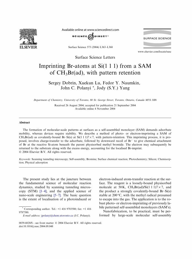
In Fig. 1(A) a typical atomically-resolved image
of the Si(1 1 1)7 · 7 surface is shown, with a unit
cell. Each unit cell has 12 Si-adatoms; 6 middle
and 6 corner [14]. At 50K adsorbed methyl bro-
mide molecules appear as bright protrusions cen-tered over the middle adatoms.
Middle adatoms in six adjacent half-unit-cells
form circles of twelve adatoms. Since these com-
prise half the adatoms, we deposited just under
50% coverage of methyl bromide to obtain the
ring-pattern of Fig. 1(B). These bright rings ex-
tended without limit. Each ring consisted of 12
CH3Br(ad) (close-up, Fig. 1(C)).Similar patterns of physisorbed molecules have
been reported for benzene (not previously for
CH3Br) on Si(1 1 1) at 78K [15]. In both cases
the bright features were observed only at low tem-
perature. The preference for physisorption on mid-
dle adatoms may be attributed to the fact that
these are more electrophilic [16,17].
In the case of CH3Br, studied here, irradiationwas found to cause reaction. Irradiation using a
photon flux of 4.0 · 1018cm�2 of 193nm excimer
radiation caused 70% of the adsorbate at 50K to
alter from the bright STM image characteristic
of physisorption to darker features at the same
site, indicative of reaction. The cross-section for
photoreaction (fractional conversion, 0.70, di-
vided by the photon flux) is �1 · 10�19cm2. Sin-gle-photon photoreaction was confirmed by the
linear intensity-dependence of rate for a 27·change in intensity. The calculated temperature in-

Fig. 1. (A) STM image of the clean Si(1 1 1)7 · 7 surface at
50K. A 7 · 7 unit cell is indicated. Vsurface = 1.5V, curren-
t = 0.2nA, �20nm · 20nm. (B) STM image of physisorbed
CH3Br(ad) on the 50K Si(1 1 1)7 · 7 surface at a coverage of
0.41 monolayer. Physisorbed molecules appear as protrusions
over the middle adatoms. Vsurface = 1.5V, current = 0.2nA,
�20nm · 20nm. (C) Zoomed-in STM image of a single ring of
physisorbed CH3Br on Si(1 1 1) surface (indicated by the dotted
circle), as in (B) but �30 A · 30A. (D) Chemisorbed Br on
Si(1 1 1) surface after photolysis of (three successive applica-
tions of) physisorbed CH3Br(ad) at 50K. Br (beneath dotted
circle) appears as depressions on the middle adatoms.
Vsurface = 1.5V current = 0.2nA, �30 A · 30A. (E) STM image
of chemisorbed Br imprints on the middle adatoms (indicated
by a dotted circle) as in (D) but with Vsurface = 2.5V. (F) STM
image of chemisorbed Br on the middle adatoms (dotted-in)
obtained by scanning (a single application of) physisorbed
CH3Br(ad) at 2.5V (scans from lower left to upper right);
Vsurface = 2.5V, current = 0.2nA, �30 A · 30A.
S. Dobrin et al. / Surface Science 573 (2004) L363–L368 L365
SURFA
CESCIEN
CE
LETTERS
crease of 5K for a total time of 10�4 s per full irra-
diation cycle of 600 laser pulses (illumination for600 · 10ns/pulse = 10�5 s, implies heating for
�10�4 s) would not result in significant thermal
reaction. Photo-desorption of the physisorbed
molecule was also observed, with a cross-section
of �3 · 10�20cm2.
On average a single exposure yielded eight Br–
Si per circle of twelve adatoms. Fig. 1(D) and
(E) were obtained from three successive adsorp-
tions, followed in each case by a total of one min-
ute of photolysis at 10Hz (i.e. �three cycles�). Whenthe bias voltage was increased from 1.5V to 2.5V
the dark ring-pattern of reaction-product in Fig.
1(D) became the bright ring-pattern of Fig. 1(E);
this �lighting-up� of atomic features with increased
surface bias-voltage is characteristic of atomic bro-
mine covalently bound to silicon at �40K [18].
Further proof that the physisorbed adsorbate
had photoreacted to produce strongly-bound Br–Si(s) was obtained by heating the pattern shown
in Fig. 1(D) and (E) to approximately 200 �C for
70s. There was no observable change, as expected
for covalent binding.
Intact CH3Br molecules would not covalently
bind to silicon. However there is extensive evi-
dence that CH3Br(ad) undergoes photoreaction
to brominate a reactive substrate [10–12,19,20].All evidence points, therefore, to Br–Si(s) as the
product of photoreaction. Since the reaction prod-
uct forms at the Si-atom beneath the parent
CH3Br(ad), we have localised photoreaction.
The localised nature of the bromination was
also demonstrated for electron-induced reaction
in which the adsorbate-covered surface was
scanned at 2.5V and the CH3Br(ad) was foundto react to form a ring pattern as for photoreaction
(Fig. 1(F)); the ring was partial since this pattern
was obtained from single scan. Scanning at in-
creased voltage resulted in some migration of
physisorbed CH3Br(ad), giving rise to the ob-
served streaks.
Facile electron-induced reaction is to be ex-
pected on the basis of the charge-transfer mecha-nism proposed for photoreaction of organic
halides at reactive surfaces [10–12,19,20]. The large
cross-section for photoinduced reaction (here, as
in earlier work) suggests UV absorption by the
substrate, rather than by the adsorbate. The nov-
elty, in the present STM study, is the localised nat-
ure of the induced surface reaction.
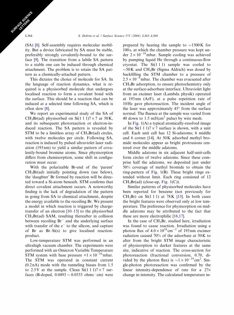
In Fig. 2 we give the results of an ab inito calcu-lation using Gaussian 98 in the MP2/3-21G*
approximation [21] for the attachment energy of
CH3Br(ad) physisorbed at a Si cluster. With the
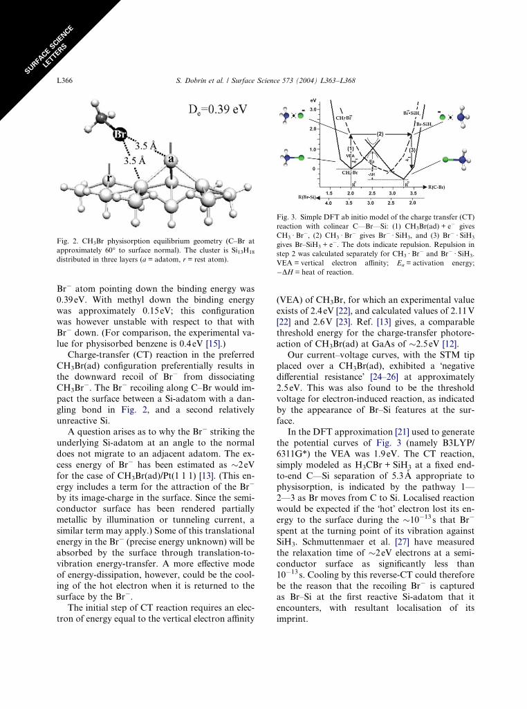
Fig. 2. CH3Br physisorption equilibrium geometry (C–Br at
approximately 60� to surface normal). The cluster is Si13H18
distributed in three layers (a = adatom, r = rest atom).
Fig. 3. Simple DFT ab initio model of the charge transfer (CT)
reaction with colinear C—Br—Si: (1) CH3Br(ad) + e� gives
CH3 Æ Br�, (2) CH3 Æ Br
� gives Br� Æ SiH3, and (3) Br� Æ SiH3
gives Br–SiH3 + e�. The dots indicate repulsion. Repulsion in
step 2 was calculated separately for CH3 Æ Br� and Br� Æ SiH3.
VEA = vertical electron affinity; Ea = activation energy;
�DH = heat of reaction.
L366 S. Dobrin et al. / Surface Science 573 (2004) L363–L368SU
RFACE
SCIENCE
LETTERS
Br� atom pointing down the binding energy was
0.39eV. With methyl down the binding energy
was approximately 0.15eV; this configurationwas however unstable with respect to that with
Br� down. (For comparison, the experimental va-
lue for physisorbed benzene is 0.4eV [15].)
Charge-transfer (CT) reaction in the preferred
CH3Br(ad) configuration preferentially results in
the downward recoil of Br� from dissociating
CH3Br�. The Br� recoiling along C–Br would im-
pact the surface between a Si-adatom with a dan-gling bond in Fig. 2, and a second relatively
unreactive Si.
A question arises as to why the Br� striking the
underlying Si-adatom at an angle to the normal
does not migrate to an adjacent adatom. The ex-
cess energy of Br� has been estimated as �2eV
for the case of CH3Br(ad)/Pt(1 1 1) [13]. (This en-
ergy includes a term for the attraction of the Br�
by its image-charge in the surface. Since the semi-
conductor surface has been rendered partially
metallic by illumination or tunneling current, a
similar term may apply.) Some of this translational
energy in the Br� (precise energy unknown) will be
absorbed by the surface through translation-to-
vibration energy-transfer. A more effective mode
of energy-dissipation, however, could be the cool-ing of the hot electron when it is returned to the
surface by the Br�.
The initial step of CT reaction requires an elec-
tron of energy equal to the vertical electron affinity
(VEA) of CH3Br, for which an experimental value
exists of 2.4eV [22], and calculated values of 2.11V
[22] and 2.6V [23]. Ref. [13] gives, a comparable
threshold energy for the charge-transfer photore-
action of CH3Br(ad) at GaAs of �2.5eV [12].
Our current–voltage curves, with the STM tipplaced over a CH3Br(ad), exhibited a �negativedifferential resistance� [24–26] at approximately
2.5eV. This was also found to be the threshold
voltage for electron-induced reaction, as indicated
by the appearance of Br–Si features at the sur-
face.
In the DFT approximation [21] used to generate
the potential curves of Fig. 3 (namely B3LYP/6311G*) the VEA was 1.9eV. The CT reaction,
simply modeled as H3CBr + SiH3 at a fixed end-
to-end C—Si separation of 5.3 A appropriate to
physisorption, is indicated by the pathway 1—
2—3 as Br moves from C to Si. Localised reaction
would be expected if the �hot� electron lost its en-
ergy to the surface during the �10�13 s that Br�
spent at the turning point of its vibration againstSiH3. Schmuttenmaer et al. [27] have measured
the relaxation time of �2eV electrons at a semi-
conductor surface as significantly less than
10�13 s. Cooling by this reverse-CT could therefore
be the reason that the recoiling Br� is captured
as Br–Si at the first reactive Si-adatom that it
encounters, with resultant localisation of its
imprint.
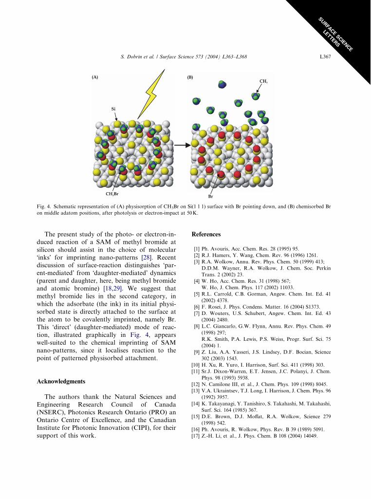
Fig. 4. Schematic representation of (A) physisorption of CH3Br on Si(1 1 1) surface with Br pointing down, and (B) chemisorbed Br
on middle adatom positions, after photolysis or electron-impact at 50K.
S. Dobrin et al. / Surface Science 573 (2004) L363–L368 L367
SURFA
CESCIEN
CE
LETTERS
The present study of the photo- or electron-in-
duced reaction of a SAM of methyl bromide at
silicon should assist in the choice of molecular
�inks� for imprinting nano-patterns [28]. Recentdiscussion of surface-reaction distinguishes �par-ent-mediated� from �daughter-mediated� dynamics
(parent and daughter, here, being methyl bromide
and atomic bromine) [18,29]. We suggest that
methyl bromide lies in the second category, in
which the adsorbate (the ink) in its initial physi-
sorbed state is directly attached to the surface at
the atom to be covalently imprinted, namely Br.This �direct� (daughter-mediated) mode of reac-
tion, illustrated graphically in Fig. 4, appears
well-suited to the chemical imprinting of SAM
nano-patterns, since it localises reaction to the
point of patterned physisorbed attachment.
Acknowledgments
The authors thank the Natural Sciences and
Engineering Research Council of Canada
(NSERC), Photonics Research Ontario (PRO) an
Ontario Centre of Excellence, and the Canadian
Institute for Photonic Innovation (CIPI), for their
support of this work.
References
[1] Ph. Avouris, Acc. Chem. Res. 28 (1995) 95.
[2] R.J. Hamers, Y. Wang, Chem. Rev. 96 (1996) 1261.
[3] R.A. Wolkow, Annu. Rev. Phys. Chem. 50 (1999) 413;
D.D.M. Wayner, R.A. Wolkow, J. Chem. Soc. Perkin
Trans. 2 (2002) 23.
[4] W. Ho, Acc. Chem. Res. 31 (1998) 567;
W. Ho, J. Chem. Phys. 117 (2002) 11033.
[5] R.L. Carrold, C.B. Gorman, Angew. Chem. Int. Ed. 41
(2002) 4378.
[6] F. Rosei, J. Phys. Condens. Matter. 16 (2004) S1373.
[7] D. Wouters, U.S. Schubert, Angew. Chem. Int. Ed. 43
(2004) 2480.
[8] L.C. Giancarlo, G.W. Flynn, Annu. Rev. Phys. Chem. 49
(1998) 297;
R.K. Smith, P.A. Lewis, P.S. Weiss, Progr. Surf. Sci. 75
(2004) 1.
[9] Z. Liu, A.A. Yasseri, J.S. Lindsey, D.F. Bocian, Science
302 (2003) 1543.
[10] H. Xu, R. Yuro, I. Harrison, Surf. Sci. 411 (1998) 303.
[11] Sr.J. Dixon-Warren, E.T. Jensen, J.C. Polanyi, J. Chem.
Phys. 98 (1993) 5938.
[12] N. Camilone III, et al., J. Chem. Phys. 109 (1998) 8045.
[13] V.A. Ukraintsev, T.J. Long, I. Harrison, J. Chem. Phys. 96
(1992) 3957.
[14] K. Takayanagi, Y. Tanishiro, S. Takahashi, M. Takahashi,
Surf. Sci. 164 (1985) 367.
[15] D.E. Brown, D.J. Moffat, R.A. Wolkow, Science 279
(1998) 542.
[16] Ph. Avouris, R. Wolkow, Phys. Rev. B 39 (1989) 5091.
[17] Z.-H. Li, et al., J. Phys. Chem. B 108 (2004) 14049.

L368 S. Dobrin et al. / Surface Science 573 (2004) L363–L368SU
RFACE
SCIENCE
LETTERS
[18] S. Dobrin, K.R. Harikumar, J.C. Polanyi, Surf. Sci. 561
(2004) 11.
[19] C.L.A. Lamont, H. Conrad, A.M. Bradshaw, Surf. Sci.
280 (1993) 79.
[20] X.L. Zhou, J.M. White, Surf. Sci. 241 (1991) 259.
[21] M.J. Frisch, et al., Gaussian 98, Gaussian, Inc., Pittsburgh
PA, 1998.
[22] A. Modelli, et al., J. Chem. Phys. 96 (1992) 2061.
[23] Z.Y. Jhou, Y.M. Xing, H. Gao, J.Mol. Struc. 542 (2001) 79.
[24] I. Lyo, P. Avouris, Science 245 (1989) 1369.
[25] J. Chen, M.A. Reed, A.M. Rawlett, J.M. Tour, Science
286 (1999) 1550.
[26] N.P. Guisinger, et al., Nano Lett. 4 (2004) 55.
[27] C.A. Schmuttenmaer, et al., Chem. Phys. 205 (1996) 91.
[28] M. Jacoby, Chem. Eng. News 78 (2000) 42.
[29] H. Rajamma et al., in preparation.
Copyright © 2022 FDOKUMEN