
Formation of discrete space-variant subwavelength dielectric gratings for polarimetric measurements
Impact of Filling Ratio on Subwavelength Optical Imaging UsingMetallic Nanolens of different Geometries
Md Ibrahim Khalil,1, 2, ∗ Md Saad-Bin-Alam,1 Atiqur Rahman,1 and Pavel A. Belov3, †
1Department of Electrical Engineering and Computer Science, North South University, Dhaka, Bangladesh2School of Electrical & Computer Engineering, Georgia Institute of Technology, Atlanta, GA-30309, USA
3Department of Photonics and Optoinformatics, St. Petersburg National Research University of Information Technologies,
Mechanics and Optics, Kronverkskiy pr., 49, 197101 St. Petersburg, Russia
compiled: August 5, 2014
Nanolens based on metallic nanorod has been considered as a prospective candidate for transporting subwave-length information. Such a lens is tuned to a particular frequency by tailoring the length of the nanorod. Inthis paper, we have investigated the impact of filling ratio on the subwavelength imaging capabilities of sucha lens. Through full-wave electromagnetic simulation, we have demonstrated that the imaging performance ofsilver (Ag) nanorod array does not only depend on the length and periodicity but also on the filling ratio orthe radius of the nanorod. We have studied this impact for nanorod having different cross-sectional shapessuch as cylindrical and triangular and examined their performances for various filling ratios.
OCIS codes: (050.6624) Subwavelength structures; (050.6628) Subwavelength nanostructures;(160.3918) Metamaterials; (180.4243) Near-field microscopy; (240.6680) Surface plasmons.
http://dx.doi.org/10.1364/XX.99.099999
1. IntroductionConventional lenses which are capable of handling onlythe far-field of a source cannot offer resolution betterthan half the operating wavelength due to diffractionlimit [1]. Imaging below the half wavelength resolu-tion (≤ λ/2) or in the order of subwavelength scale re-quires capturing near-field which decays exponentiallyas it travels away from the source to free space or anynaturally available media. In order to achieve that ob-jective, several imaging techniques have been proposedin the last decade those include perfect lens, silver super-lens, hyper-lens, stimulated emission depletion (STED)fluorescence microscope etc. [2–8]. Besides these, metal-lic wire array as subwavelength imaging system has alsobeen proposed in [9, 10] that allows simulteneous imag-ing of the whole area of interest in contrast to the time-consuming point-by-point scanning by a single probe ofa near-field scanning optical microscope (NSOM) [2–4].A complete procedure to model such a metallic nanowirebased lens for near-field imaging in the visible range isdiscussed in [11–13]. Such a lens functions due to theexcitation of surface plasmon polaritons (SPP) at themetal-dielectric interface that actually transport sub-wavelength information of a source from one side of the
∗ Corresponding author: [email protected] or,[email protected]; First two authors contributedequally towards this work† Corresponding author: [email protected]
lens to the other side.
c)b)a)
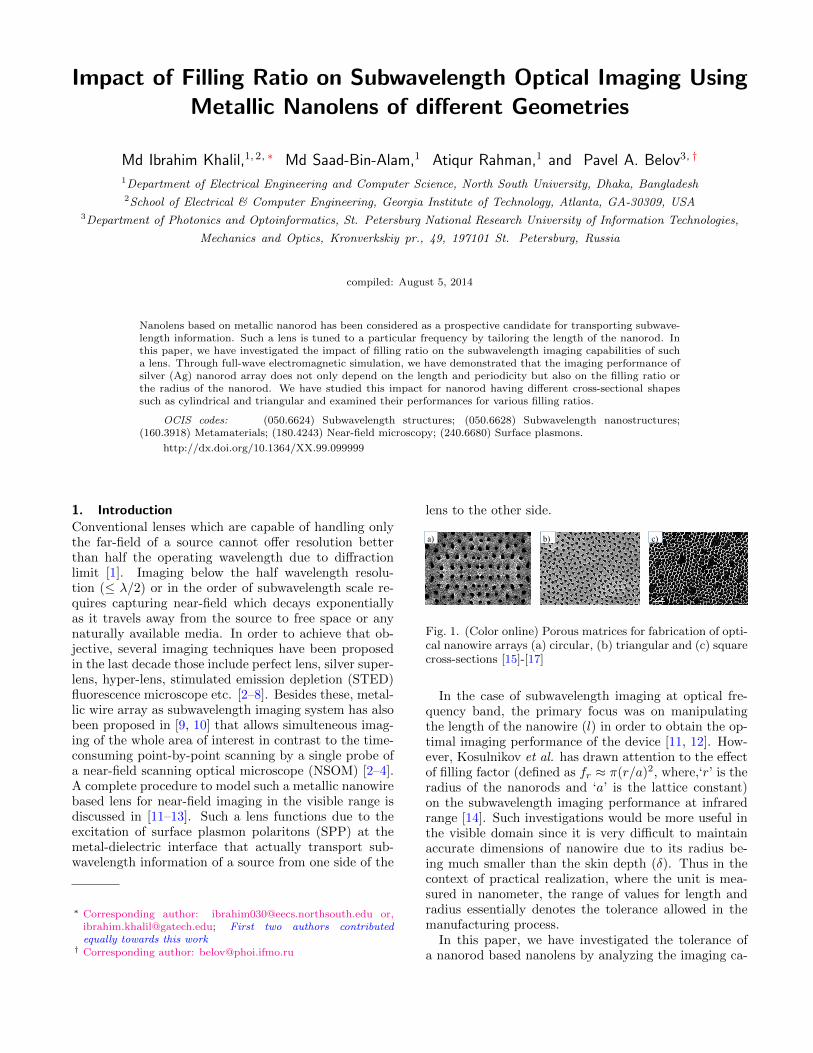
Fig. 1. (Color online) Porous matrices for fabrication of opti-cal nanowire arrays (a) circular, (b) triangular and (c) squarecross-sections [15]-[17]
In the case of subwavelength imaging at optical fre-quency band, the primary focus was on manipulatingthe length of the nanowire (l) in order to obtain the op-timal imaging performance of the device [11, 12]. How-ever, Kosulnikov et al. has drawn attention to the effectof filling factor (defined as fr ≈ π(r/a)2, where,‘r’ is theradius of the nanorods and ‘a’ is the lattice constant)on the subwavelength imaging performance at infraredrange [14]. Such investigations would be more useful inthe visible domain since it is very difficult to maintainaccurate dimensions of nanowire due to its radius be-ing much smaller than the skin depth (δ). Thus in thecontext of practical realization, where the unit is mea-sured in nanometer, the range of values for length andradius essentially denotes the tolerance allowed in themanufacturing process.
In this paper, we have investigated the tolerance ofa nanorod based nanolens by analyzing the imaging ca-
2
3𝑎𝑎
𝑎𝑎
yz
2r
𝑎𝑎
3𝑎𝑎
𝑎𝑎
yz
𝑎𝑎
x
y
z
(c) (d) (e)
r
x
yz
x
y
z
2r
inpu
toutputPBC
PBC
PMC
PMC
Discrete point sources
(a)(b)
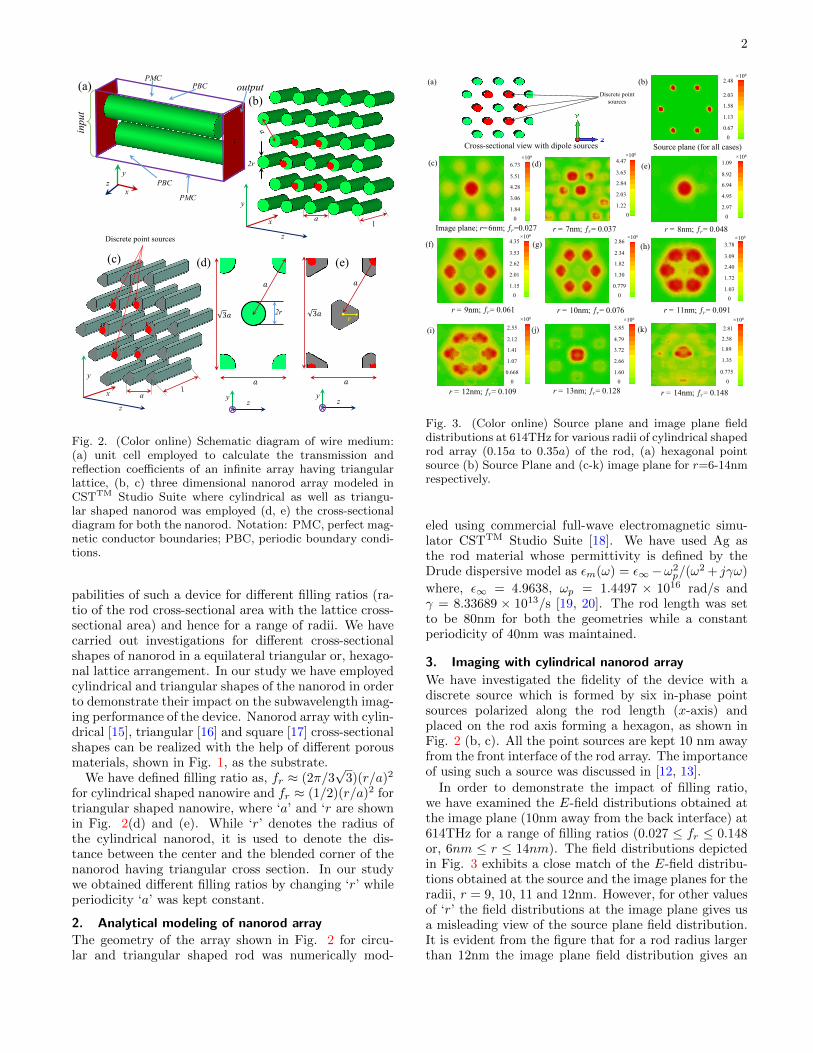
Fig. 2. (Color online) Schematic diagram of wire medium:(a) unit cell employed to calculate the transmission andreflection coefficients of an infinite array having triangularlattice, (b, c) three dimensional nanorod array modeled inCSTTM Studio Suite where cylindrical as well as triangu-lar shaped nanorod was employed (d, e) the cross-sectionaldiagram for both the nanorod. Notation: PMC, perfect mag-netic conductor boundaries; PBC, periodic boundary condi-tions.
pabilities of such a device for different filling ratios (ra-tio of the rod cross-sectional area with the lattice cross-sectional area) and hence for a range of radii. We havecarried out investigations for different cross-sectionalshapes of nanorod in a equilateral triangular or, hexago-nal lattice arrangement. In our study we have employedcylindrical and triangular shapes of the nanorod in orderto demonstrate their impact on the subwavelength imag-ing performance of the device. Nanorod array with cylin-drical [15], triangular [16] and square [17] cross-sectionalshapes can be realized with the help of different porousmaterials, shown in Fig. 1, as the substrate.
We have defined filling ratio as, fr ≈ (2π/3√
3)(r/a)2
for cylindrical shaped nanowire and fr ≈ (1/2)(r/a)2 fortriangular shaped nanowire, where ‘a’ and ‘r are shownin Fig. 2(d) and (e). While ‘r’ denotes the radius ofthe cylindrical nanorod, it is used to denote the dis-tance between the center and the blended corner of thenanorod having triangular cross section. In our studywe obtained different filling ratios by changing ‘r’ whileperiodicity ‘a’ was kept constant.
2. Analytical modeling of nanorod arrayThe geometry of the array shown in Fig. 2 for circu-lar and triangular shaped rod was numerically mod-
1.84
0
(a)
Cross-sectional view with dipole sources Source plane (for all cases)
Image plane; r=6nm; 𝑓𝑓𝑟𝑟=0.027
(b)
(c) (d)
r = 7nm; 𝑓𝑓𝑟𝑟= 0.037
r = 14nm; 𝑓𝑓𝑟𝑟= 0.148r = 13nm; 𝑓𝑓𝑟𝑟= 0.128r = 12nm; 𝑓𝑓𝑟𝑟= 0.109
(i) (j) (k)
Discrete point sources
2.48
2.03
1.58
1.13
0.670
6.73
5.51
4.28
3.06
0
4.47
3.65
2.84
2.03
1.220
2.81
2.38
1.89
1.35
0.775
0
5.85
4.79
3.72
2.66
1.600
2.55
2.12
1.41
1.07
0.6680
r = 8nm; 𝑓𝑓𝑟𝑟= 0.048
(e) 1.09
8.92
6.94
4.95
2.970
r = 9nm; 𝑓𝑓𝑟𝑟= 0.061 r = 10nm; 𝑓𝑓𝑟𝑟= 0.076
(f) (g)4.35
3.53
2.62
2.01
1.15
2.86
2.34
1.82
1.30
0.7790
r = 11nm; 𝑓𝑓𝑟𝑟= 0.091
(h) 3.78
3.09
2.40
1.72
1.030
×106
×106
×106
×106×106×106
×106 ×106
×106 ×106
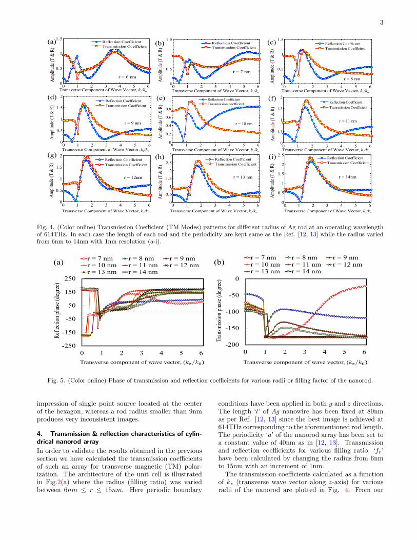
Fig. 3. (Color online) Source plane and image plane fielddistributions at 614THz for various radii of cylindrical shapedrod array (0.15a to 0.35a) of the rod, (a) hexagonal pointsource (b) Source Plane and (c-k) image plane for r=6-14nmrespectively.
eled using commercial full-wave electromagnetic simu-lator CSTTM Studio Suite [18]. We have used Ag asthe rod material whose permittivity is defined by theDrude dispersive model as εm(ω) = ε∞−ω2
p/(ω2 + jγω)
where, ε∞ = 4.9638, ωp = 1.4497 × 10¹⁶ rad/s andγ = 8.33689 × 10¹³/s [19, 20]. The rod length was setto be 80nm for both the geometries while a constantperiodicity of 40nm was maintained.
3. Imaging with cylindrical nanorod array
We have investigated the fidelity of the device with adiscrete source which is formed by six in-phase pointsources polarized along the rod length (x-axis) andplaced on the rod axis forming a hexagon, as shown inFig. 2 (b, c). All the point sources are kept 10 nm awayfrom the front interface of the rod array. The importanceof using such a source was discussed in [12, 13].
In order to demonstrate the impact of filling ratio,we have examined the E-field distributions obtained atthe image plane (10nm away from the back interface) at614THz for a range of filling ratios (0.027 ≤ fr ≤ 0.148or, 6nm ≤ r ≤ 14nm). The field distributions depictedin Fig. 3 exhibits a close match of the E-field distribu-tions obtained at the source and the image planes for theradii, r = 9, 10, 11 and 12nm. However, for other valuesof ‘r’ the field distributions at the image plane gives usa misleading view of the source plane field distribution.It is evident from the figure that for a rod radius largerthan 12nm the image plane field distribution gives an
3
(a) (c)(b)
(h)(g)
(e) (f)(d)
(i)
Transverse Component of Wave Vector, kz/ko Transverse Component of Wave Vector, kz/ko Transverse Component of Wave Vector, kz/ko
Transverse Component of Wave Vector, kz/ko Transverse Component of Wave Vector, kz/ko Transverse Component of Wave Vector, kz/ko
Transverse Component of Wave Vector, kz/koTransverse Component of Wave Vector, kz/koTransverse Component of Wave Vector, kz/ko
Ampli
tude (
T &
R)
Ampli
tude (
T &
R)
Ampli
tude (
T &
R)
Ampli
tude (
T &
R)
Ampli
tude (
T &
R)
Ampli
tude (
T &
R)Am
plitud
e (T
& R)
Ampli
tude (
T &
R)
Ampli
tude (
T &
R)
0 1 2 3 4 5 60
0.5
1
1.5
Reflection CoefficientTransmission Coefficient
r = 6 nm
0 1 2 3 4 5 60
0.5
1
1.5
Reflection CoefficientTransmission Coefficient
r = 7 nm
0 1 2 3 4 5 60
0.5
1
1.5
2
Reflection CoefficientTransmission Coefficient
r = 12nm
0 1 2 3 4 5 60
0.5
1
1.5
2
2.5
3
Reflection CoefficientTransmission Coefficient
r = 13 nm
0 1 2 3 4 5 60
0.5
1
1.5
2
2.5
Reflection CoefficientTransmission Coefficient
r = 14nm
0 1 2 3 4 5 60
0.5
1
1.5
Reflection CoefficientTransmission Coefficient
r = 8 nm
0 1 2 3 4 5 60
0.5
1
1.5
2
Reflection CoefficientTransmission Coefficient
r = 9 nm
0 1 2 3 4 5 60
0.2
0.4
0.6
0.8
1
Reflection CoefficientTransmission coefficient
r = 10 nm
0 1 2 3 4 5 60
0.5
1
1.5
2
Reflection CoefficientTransmission Coefficient
r = 11 nm
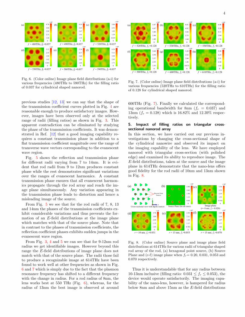
Fig. 4. (Color online) Transmission Coefficient (TM Modes) patterns for different radius of Ag rod at an operating wavelengthof 614THz. In each case the length of each rod and the periodicity are kept same as the Ref. [12, 13] while the radius variedfrom 6nm to 14nm with 1nm resolution (a-i).
-250
-150
-50
50
150
250
0 1 2 3 4 5 6
r = 7 nm r = 8 nm r = 9 nmr = 10 nm r = 11 nm r = 12 nmr = 13 nm r = 14 nm
-200
-150
-100
-50
0
0 1 2 3 4 5 6
r = 7 nm r = 8 nm r = 9 nmr = 10 nm r = 11 nm r = 12 nmr = 13 nm r = 14 nm
Transverse component of wave vector, (𝑘𝑘𝑧𝑧/𝑘𝑘0)
Tran
smiss
ion ph
ase (
degr
ee)
Transverse component of wave vector, (𝑘𝑘𝑧𝑧/𝑘𝑘0)
Refle
ction
phas
e (de
gree
)
(a) (b)
Fig. 5. (Color online) Phase of transmission and reflection coefficients for various radii or filling factor of the nanorod.
impression of single point source located at the centerof the hexagon, whereas a rod radius smaller than 9nmproduces very inconsistent images.
4. Transmission & reflection characteristics of cylin-drical nanorod array
In order to validate the results obtained in the previoussection we have calculated the transmission coefficientsof such an array for transverse magnetic (TM) polar-ization. The architecture of the unit cell is illustratedin Fig.2(a) where the radius (filling ratio) was variedbetween 6nm ≤ r ≤ 15nm. Here periodic boundary
conditions have been applied in both y and z directions.The length ‘l’ of Ag nanowire has been fixed at 80nmas per Ref. [12, 13] since the best image is achieved at614THz corresponding to the aforementioned rod length.The periodicity ‘a’ of the nanorod array has been set toa constant value of 40nm as in [12, 13]. Transmissionand reflection coefficients for various filling ratio, ‘fr’have been calculated by changing the radius from 6nmto 15nm with an increment of 1nm.
The transmission coefficients calculated as a functionof kz (transverse wave vector along z-axis) for variousradii of the nanorod are plotted in Fig. 4. From our
4
f = 520THz, 𝑓𝑓𝑟𝑟=0.037
(c)
(f)
f = 490THz, 𝑓𝑓𝑟𝑟=0.037
(a) (b)
(d) (e)
f = 580THz, 𝑓𝑓𝑟𝑟=0.037f = 550THz, 𝑓𝑓𝑟𝑟=0.037
f = 480THz, 𝑓𝑓𝑟𝑟=0.037
f = 590THz, 𝑓𝑓𝑟𝑟=0.037
4.19
3.43
2.67
1.91
1.140
5.34
4.37
3.40
2.43
1.460
6.26
5.13
3.99
2.85
1.710
3.06
2.51
1.95
1.39
0.8350
4.70
3.84
2.99
2.13
1.280
3.12
2.55
1.99
1.42
0.8510
×106 ×106 ×106
×106×106×106
Fig. 6. (Color online) Image plane field distributions (a-i) forvarious frequencies (480THz to 590THz) for the filling ratioof 0.037 for cylindrical shaped nanorod.
previous studies [12, 13] we can say that the shape ofthe transmission coefficient curves plotted in Fig. 4 arereasonable enough to produce satisfactory images. How-ever, images have been observed only at the selectedrange of radii (filling ratios) as shown in Fig. 3. Thisapparent contradiction can be eliminated by studyingthe phase of the transmission coefficients. It was demon-strated in Ref. [12] that a good imaging capability re-quires a constant transmission phase in addition to aflat transmission coefficient magnitude over the range oftransverse wave vectors corresponding to the evanescentwave region.
Fig. 5 shows the reflection and transmission phasefor different radii varying from 7 to 14nm. It is evi-dent that rod radii from 9 to 12nm produces constantphase while the rest demonstrates significant variationsover the ranges of evanescent harmonics. A constanttransmission phase ensures that all evanescent harmon-ics propagate through the rod array and reach the im-age plane simultaneously. Any variation appearing inthe transmission phase leads to distortion and hence amisleading image of the source.
From Fig. 5 we see that for the rod radii of 7, 8, 13and 14nm the phases of the transmission coefficients ex-hibit considerable variations and thus prevents the for-mation of an E-field distributions at the image planewhich matches with that of the source plane. Note thatin contrast to the phases of transmission coefficients, thereflection coefficient phases exhibits sudden jumps in theevanescent wave region.
From Fig. 3, 4 and 5 we can see that for 9-12nm rodradius we get identifiable images. However beyond thisrange the E-field distributions of image plane does notmatch with that of the source plane. The radii those failto produce a recognizable image at 614THz have beenfound to work well at other frequencies as shown in Fig.6 and 7 which is simply due to the fact that the plasmonresonance frequency has shifted to a different frequencywith the change in radius. For a rod radius of 8nm, thelens works best at 550 THz (Fig. 6), whereas, for theradius of 13nm the best image is observed at around
f = 550THz, 𝑓𝑓𝑟𝑟=0.128
f = 580THz, 𝑓𝑓𝑟𝑟=0.128 f = 600THz, 𝑓𝑓𝑟𝑟=0.128
(c)
(h)
f = 530THz, 𝑓𝑓𝑟𝑟=0.128
(a) (b)
(g)(f)
f = 520THz, 𝑓𝑓𝑟𝑟=0.128
f = 610THz, 𝑓𝑓𝑟𝑟=0.128
6.01
4.92
3.82
2.73
1.640
3.20
2.62
2.04
1.46
0.8730
5.20
4.25
3.31
2.36
1.420
5.60
4.58
3.57
2.55
1.530
6.46
5.29
4.11
2.94
1.760
5.47
4.47
3.48
2.48
1.490
×106 ×106 ×106
×106×106×106
Fig. 7. (Color online) Image plane field distributions (a-i) forvarious frequencies (520THz to 610THz) for the filling ratioof 0.128 for cylindrical shaped nanorod.
600THz (Fig. 7). Finally we calculated the correspond-ing operational bandwidth for 8nm (fr = 0.037) and13nm (fr = 0.128) which is 16.82% and 12.39% respec-tively.
5. Impact of filling ratios on triangular cross-sectional nanorod arrayIn this section, we have carried out our previous in-vestigations by changing the cross-sectional shape ofthe cylindrical nanowire and observed its impact onthe imaging capability of the lens. We have employednanorod with triangular cross-section (with polishededge) and examined its ability to reproduce image. TheE-field distributions, taken at the source and the imageplane in 614THz demonstrate that the nano-lens offersgood fidelity for the rod radii of 10nm and 13nm shownin Fig. 8.
Image plane (r= 8 nm; 𝑓𝑓𝑟𝑟= 0.020)
r = 10 nm; 𝑓𝑓𝑟𝑟=0.031 r = 13 nm; 𝑓𝑓𝑟𝑟=0.053 r = 15 nm; 𝑓𝑓𝑟𝑟=0.070
(c)
(f)
Source Plane (for all cases)
Discrete Point Sources
(a) (b)
(d) (e)
Cross-sectional view with dipole sources
3.36
2.75
2.14
1.53
0.9160
3.89
3.18
2.47
1.77
1.060
2.48
2.03
1.58
1.13
0.680
2.58
2.11
1.64
1.17
0.7030
3.78
3.09
2.40
1.72
1.030
×106 ×106
×106 ×106 ×106
Fig. 8. (Color online) Source plane and image plane fielddistributions at 614THz for various radii of triangular shapedrod array of the rod, (a) hexagonal point source, (b) SourcePlane and (c-f) image plane when fr= 0.20, 0.031, 0.053 and0.070 respectively.
Thus it is understandable that for any radius between10-13nm inclusive (filling ratio: 0.031 ≤ fr ≤ 0.053), thedevice would operate satisfactorily. The imaging capa-bility of the nano-lens, however, is hampered for radiusbelow 8nm and above 15nm as the E-field distributions
5
Transverse Component of Wave Vector, kz/ko
Transverse Component of Wave Vector, kz/ko
Transverse Component of Wave Vector, kz/ko
Transverse Component of Wave Vector, kz/ko
Am
plitu
de (T
& R
)
Am
plitu
de (T
& R
)
Am
plitu
de (T
& R
)
Am
plitu
de (T
& R
)
(a) (b)
(c) (d)
0 1 2 3 4 5 60
0.2
0.4
0.6
0.8
1
1.2
Transmission CoefficientsReflection Coefficients
0 1 2 3 4 5 60
0.20.40.60.8
11.2
Transmission CoefficientsReflection Coefficients
0 1 2 3 4 5 60
0.5
1
1.5
2
Transmission CoefficientsReflection Coefficients
0 1 2 3 4 5 60
0.20.40.60.8
11.21.4
Transmission CoeffecientsReflection Coeffecients
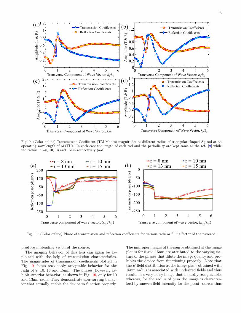
Fig. 9. (Color online) Transmission Coefficient (TM Modes) magnitudes at different radius of triangular shaped Ag rod at anoperating wavelength of 614THz. In each case the length of each rod and the periodicity are kept same as the ref. [9] whilethe radius, r =8, 10, 13 and 15nm respectively (a-d)
-250
-200
-150
-100
-50
0
0 1 2 3 4 5 6
r = 8 nm r = 10 nmr = 13 nm r = 15 nm
-250
-150
-50
50
150
250
0 1 2 3 4 5 6
r = 8 nm r = 10 nmr = 13 nm r = 15 nm
Transverse component of wave vector, (𝑘𝑘𝑧𝑧/𝑘𝑘0)
Tran
smiss
ion
phas
e (de
gree
)
Transverse component of wave vector, (𝑘𝑘𝑧𝑧/𝑘𝑘0)
Refle
ctio
n ph
ase (
degr
ee)
(a) (b)
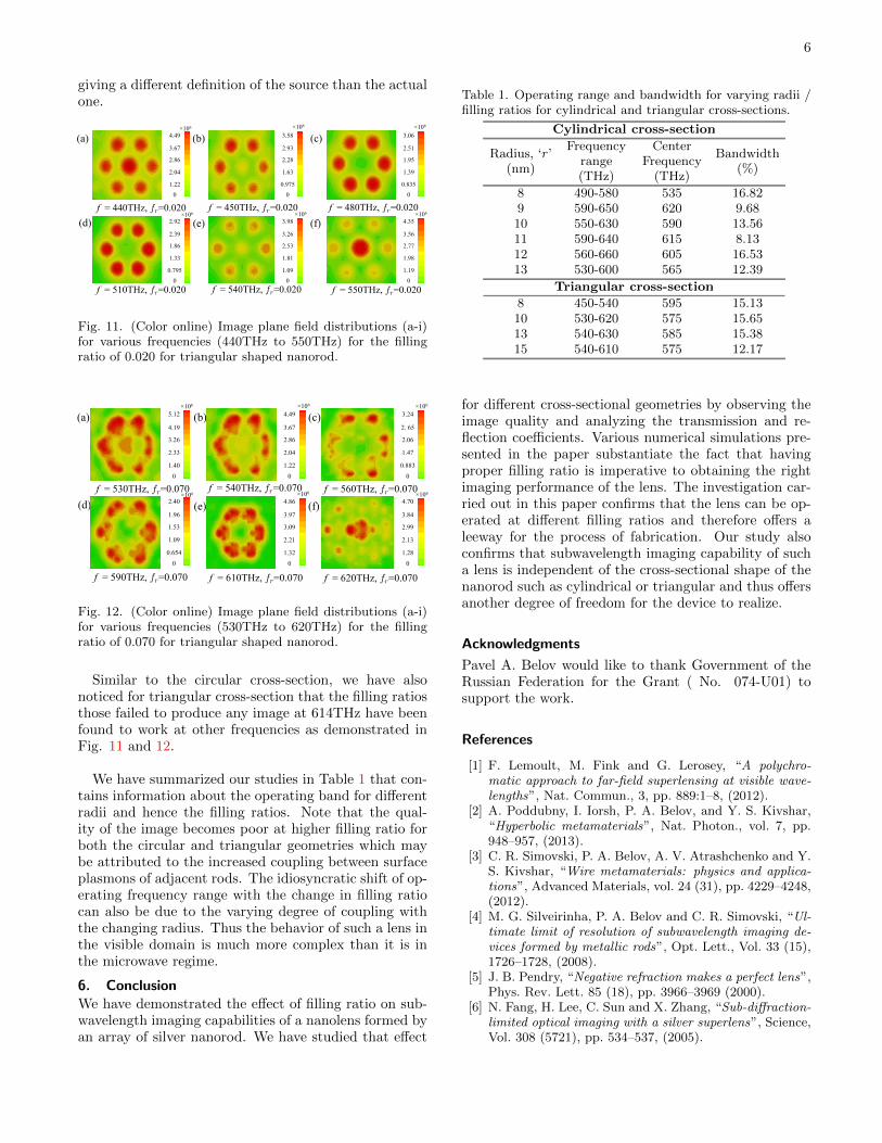
Fig. 10. (Color online) Phase of transmission and reflection coefficients for various radii or filling factor of the nanorod.
produce misleading vision of the source.The imaging behavior of this lens can again be ex-
plained with the help of transmission characteristics.The magnitudes of transmission coefficients plotted inFig. 9 shows reasonably acceptable behavior for theradii of 8, 10, 13 and 15nm. The phases, however, ex-hibit superior behavior, as shown in Fig. 10, only for 10and 13nm radii. They demonstrate non-varying behav-ior that actually enable the device to function properly.
The improper images of the source obtained at the imageplanes for 8 and 15nm are attributed to the varying na-ture of the phases that dilute the image quality and pro-hibits the device from functioning properly. Note thatthe E-field distribution at the image plane obtained with15nm radius is associated with undesired fields and thusresults in a very noisy image that is hardly recognizable,whereas, for the radius of 8nm the image is character-ized by uneven field intensity for the point sources thus
6
giving a different definition of the source than the actualone.
(c)
(f)
(a) (b)
(d) (e)f = 440THz, 𝑓𝑓𝑟𝑟=0.020 f = 450THz, 𝑓𝑓𝑟𝑟=0.020 f = 480THz, 𝑓𝑓𝑟𝑟=0.020
f = 510THz, 𝑓𝑓𝑟𝑟=0.020 f = 540THz, 𝑓𝑓𝑟𝑟=0.020 f = 550THz, 𝑓𝑓𝑟𝑟=0.020
3.58
2.93
2.28
1.63
0.9750
3.98
3.26
2.53
1.81
1.090
3.06
2.51
1.95
1.39
0.8350
4.49
3.67
2.86
2.04
1.220
4.35
3.56
2.77
1.98
1.190
2.92
2.39
1.86
1.33
0.7950
×106 ×106 ×106
×106×106×106
Fig. 11. (Color online) Image plane field distributions (a-i)for various frequencies (440THz to 550THz) for the fillingratio of 0.020 for triangular shaped nanorod.
(c)
(f)
(a) (b)
(d) (e)f = 530THz, 𝑓𝑓𝑟𝑟=0.070 f = 540THz, 𝑓𝑓𝑟𝑟=0.070 f = 560THz, 𝑓𝑓𝑟𝑟=0.070
f = 590THz, 𝑓𝑓𝑟𝑟=0.070 f = 610THz, 𝑓𝑓𝑟𝑟=0.070 f = 620THz, 𝑓𝑓𝑟𝑟=0.070
4.70
3.84
2.99
2.13
1.280
3.24
2. 65
2.06
1.47
0.8830
4.86
3.97
3.09
2.21
1.320
4.49
3.67
2.86
2.04
1.220
2.40
1.96
1.53
1.09
0.6540
5.12
4.19
3.26
2.33
1.400
×106 ×106 ×106
×106×106×106
Fig. 12. (Color online) Image plane field distributions (a-i)for various frequencies (530THz to 620THz) for the fillingratio of 0.070 for triangular shaped nanorod.
Similar to the circular cross-section, we have alsonoticed for triangular cross-section that the filling ratiosthose failed to produce any image at 614THz have beenfound to work at other frequencies as demonstrated inFig. 11 and 12.
We have summarized our studies in Table 1 that con-tains information about the operating band for differentradii and hence the filling ratios. Note that the qual-ity of the image becomes poor at higher filling ratio forboth the circular and triangular geometries which maybe attributed to the increased coupling between surfaceplasmons of adjacent rods. The idiosyncratic shift of op-erating frequency range with the change in filling ratiocan also be due to the varying degree of coupling withthe changing radius. Thus the behavior of such a lens inthe visible domain is much more complex than it is inthe microwave regime.
6. ConclusionWe have demonstrated the effect of filling ratio on sub-wavelength imaging capabilities of a nanolens formed byan array of silver nanorod. We have studied that effect
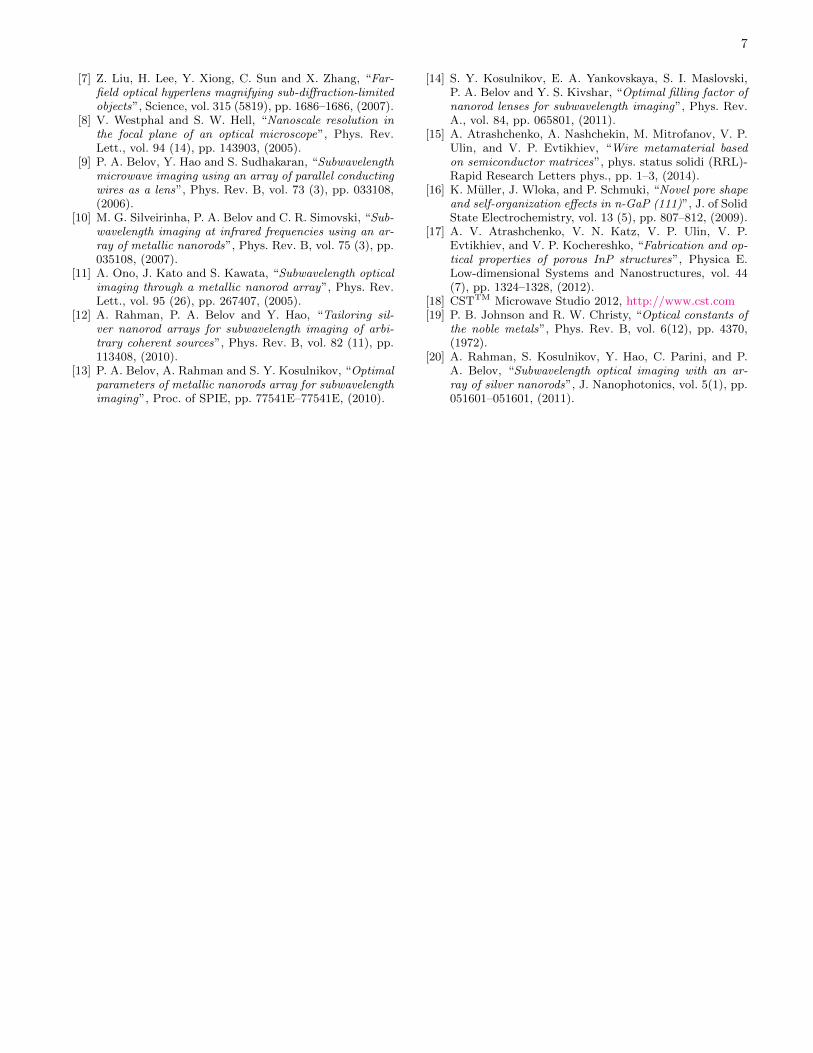
Table 1. Operating range and bandwidth for varying radii /filling ratios for cylindrical and triangular cross-sections.
Cylindrical cross-section
Radius, ‘r’(nm)
Frequencyrange(THz)
CenterFrequency
(THz)
Bandwidth(%)
8 490-580 535 16.829 590-650 620 9.6810 550-630 590 13.5611 590-640 615 8.1312 560-660 605 16.5313 530-600 565 12.39
Triangular cross-section
8 450-540 595 15.1310 530-620 575 15.6513 540-630 585 15.3815 540-610 575 12.17
for different cross-sectional geometries by observing theimage quality and analyzing the transmission and re-flection coefficients. Various numerical simulations pre-sented in the paper substantiate the fact that havingproper filling ratio is imperative to obtaining the rightimaging performance of the lens. The investigation car-ried out in this paper confirms that the lens can be op-erated at different filling ratios and therefore offers aleeway for the process of fabrication. Our study alsoconfirms that subwavelength imaging capability of sucha lens is independent of the cross-sectional shape of thenanorod such as cylindrical or triangular and thus offersanother degree of freedom for the device to realize.
Acknowledgments
Pavel A. Belov would like to thank Government of theRussian Federation for the Grant ( No. 074-U01) tosupport the work.
References
[1] F. Lemoult, M. Fink and G. Lerosey, “A polychro-matic approach to far-field superlensing at visible wave-lengths”, Nat. Commun., 3, pp. 889:1–8, (2012).
[2] A. Poddubny, I. Iorsh, P. A. Belov, and Y. S. Kivshar,“Hyperbolic metamaterials”, Nat. Photon., vol. 7, pp.948–957, (2013).
[3] C. R. Simovski, P. A. Belov, A. V. Atrashchenko and Y.S. Kivshar, “Wire metamaterials: physics and applica-tions”, Advanced Materials, vol. 24 (31), pp. 4229–4248,(2012).
[4] M. G. Silveirinha, P. A. Belov and C. R. Simovski, “Ul-timate limit of resolution of subwavelength imaging de-vices formed by metallic rods”, Opt. Lett., Vol. 33 (15),1726–1728, (2008).
[5] J. B. Pendry, “Negative refraction makes a perfect lens”,Phys. Rev. Lett. 85 (18), pp. 3966–3969 (2000).
[6] N. Fang, H. Lee, C. Sun and X. Zhang, “Sub-diffraction-limited optical imaging with a silver superlens”, Science,Vol. 308 (5721), pp. 534–537, (2005).
7
[7] Z. Liu, H. Lee, Y. Xiong, C. Sun and X. Zhang, “Far-field optical hyperlens magnifying sub-diffraction-limitedobjects”, Science, vol. 315 (5819), pp. 1686–1686, (2007).
[8] V. Westphal and S. W. Hell, “Nanoscale resolution inthe focal plane of an optical microscope”, Phys. Rev.Lett., vol. 94 (14), pp. 143903, (2005).
[9] P. A. Belov, Y. Hao and S. Sudhakaran, “Subwavelengthmicrowave imaging using an array of parallel conductingwires as a lens”, Phys. Rev. B, vol. 73 (3), pp. 033108,(2006).
[10] M. G. Silveirinha, P. A. Belov and C. R. Simovski, “Sub-wavelength imaging at infrared frequencies using an ar-ray of metallic nanorods”, Phys. Rev. B, vol. 75 (3), pp.035108, (2007).
[11] A. Ono, J. Kato and S. Kawata, “Subwavelength opticalimaging through a metallic nanorod array”, Phys. Rev.Lett., vol. 95 (26), pp. 267407, (2005).
[12] A. Rahman, P. A. Belov and Y. Hao, “Tailoring sil-ver nanorod arrays for subwavelength imaging of arbi-trary coherent sources”, Phys. Rev. B, vol. 82 (11), pp.113408, (2010).
[13] P. A. Belov, A. Rahman and S. Y. Kosulnikov, “Optimalparameters of metallic nanorods array for subwavelengthimaging”, Proc. of SPIE, pp. 77541E–77541E, (2010).
[14] S. Y. Kosulnikov, E. A. Yankovskaya, S. I. Maslovski,P. A. Belov and Y. S. Kivshar, “Optimal filling factor ofnanorod lenses for subwavelength imaging”, Phys. Rev.A., vol. 84, pp. 065801, (2011).
[15] A. Atrashchenko, A. Nashchekin, M. Mitrofanov, V. P.Ulin, and V. P. Evtikhiev, “Wire metamaterial basedon semiconductor matrices”, phys. status solidi (RRL)-Rapid Research Letters phys., pp. 1–3, (2014).
[16] K. Muller, J. Wloka, and P. Schmuki, “Novel pore shapeand self-organization effects in n-GaP (111)”, J. of SolidState Electrochemistry, vol. 13 (5), pp. 807–812, (2009).
[17] A. V. Atrashchenko, V. N. Katz, V. P. Ulin, V. P.Evtikhiev, and V. P. Kochereshko, “Fabrication and op-tical properties of porous InP structures”, Physica E.Low-dimensional Systems and Nanostructures, vol. 44(7), pp. 1324–1328, (2012).
[18] CSTTM Microwave Studio 2012, http://www.cst.com[19] P. B. Johnson and R. W. Christy, “Optical constants of
the noble metals”, Phys. Rev. B, vol. 6(12), pp. 4370,(1972).
[20] A. Rahman, S. Kosulnikov, Y. Hao, C. Parini, and P.A. Belov, “Subwavelength optical imaging with an ar-ray of silver nanorods”, J. Nanophotonics, vol. 5(1), pp.051601–051601, (2011).
Copyright © 2022 FDOKUMEN