Hynix PowerPoint template
41
-
Upload
khangminh22 -
Category
Documents
-
view
0 -
download
0
Transcript of Hynix PowerPoint template

Contents
1.Introduction
2. Flash Cell Structure & Array
3. Flash Cell Vt Distribution
4. Reliability

1.Introduction

WL
BL
Capacitor
WL
BL
FG
WL
BL
F-Cap.
BL BL
Load
Vss
Vcc
WL
Volatile Memories Non-volatile Memories
DRAM SRAM FeRAM FG
1T + 1C 6Tr or 4Tr + 2Load 1T + 1C 1T
Refresh Non-refresh Non-refresh Non-refresh
Fast, Low-cost Very Fast, High-cost Fast, Very High-cost Slow, Low-cost
SDRAM/EDO
DDR/QDR, RAMBUS
SRAM , Pseudo SRAM Mask ROM, EPROM, EEPROM , Flash
Various non-volatile memories (PRAM, RRAM,MRAM…) nowadays!
Flash Memory is one among FG (Floating Gate) non-volatile memories.
Semiconductor Memory
Introduction
Page 4

Floating Gate NVM
Flash ? ; Erase by Bit Erase by sector/block
EPROM EEPROM Flash
Chip Erase Erasing using FN Sector/Block Erase using FN
Mask ROM
PR
n+
Implant
n+ n+
Mask ROM
EPROM EEPROM Flash
W/L
B/L
W/L
B/L
Sector/Block
W/L
B/L
Chip
- PGM by Mask
- Non-Erasable
- 1 Tr. Cell
- PGM Electrically ( CHEI)
- UV Chip Erasable
- 2 Tr. Cell
- PGM Electrically ( FN)
- Byte Erasable ( FN)
- 1 Tr. Cell
- PGM Electrically ( CHEI/ FN)
- Sector/Block Erasable (FN)
1984 Toshiba 1979 Intel 1971 Intel
Introduction
Page 5

Flash Memory Classification
FLASH MEMORY
NOR NAND
Virtual GND Common GND AND ARRAY
Organization
ACT Virtual GND
Contactless
AMG
Split
Gate
(SST)
Source
Injection
Standard
(NOR) DINOR EEPROM HiCR
AND
CELL
Poly-Poly Erase Merged
1. Cell Array Category
Page 6
Introduction

NOR Flash NAND Flash
NOR Flash
PDA Modem
PC Bios
Mobile Phone
HDD Driver
DVD Player
NAND Flash
Memory Card
Digital Camera MP3
Voice Recoder
Introduction
Page 7

MultiMediaCard
SD Card
MemoryStick
Compact Flash
Memory Cards Applications
License ; Free
One I/O Port
Low Speed
One Chip PKG
License ; Not Free
Four I/O Port
Medium Speed
Support Security
One chip PKG
Sony compatible only
M/S ( ~ 64Mb)
M/S Pro ( 128Mb ~)
License ; Not Free
Eight I/O Port
Highest Speed
High density ( 4 Chip PKG)
High performance Disk
Page 8
Introduction

State-of-the-art 0.7mm PKG provides high reliability and low-cost
64 UELP Controller 0.7mm WSOP
MMC Thickness 1.4mm
Flash Die Flash Die 0.7mm
Normal MMC Vertical Structure
24mm
Controller
Flash
32mm
Normal MMC RS MMC
3 Chip Stack
Flash Die Flash Die Controll
er
24mm
18mm Controller
Die Flash Die
SIP (System In Package) Technology
Introduction
Page 9

Introduction
Multi-Chip Package
SDP DDP QDP
Density 1Gb 2Gb 4Gb
Cell String 32
Page Size (2048 + 64)Bytes
# of Block 2048 4096 8192
Flash Die
Flash Die
Flash Die Flash Die
Flash Die
Flash Die Flash Die SDP
DDP
QDP
•One CE# Multi-Chip Package
SDP, DDP, QDP
•Multi CE# Multi-Chip
SDP, DDP
1st chip 2nd chip 3rd chip
4th chip
1CE# 2CE#
Two CE# DDP
1st CE# 2nd CE#
SDP DDP SDP QDP
Density 1Gb 2Gb 2Gb 4Gb
Cell String 32
Page Size (2048 + 64)Bytes
# of Block 2048 4096 2048 4096
Two CE# Multi-Chip Package
One CE# Multi-Chip Package
Page 10

2. Flash Cell Structure & Array

Source Drain TOX FG
CG GOX
NWELL
PWELL
P-SUB
Material Charactor
FG Type 도체
(PolySilicon)
*Less Compatible with CMOS Tech.
*Thickness of Tunnel Oxide > 7nm
*Large Distribution of Vth
*Shrink Limitation
*Cell-to-Cell Interference
SONOSType 부도체
(SiN, …)
*More Compatible with CMOS Tech.
*More scaling capability
*Higher Speed
*Reliability Issue ( Cycling, … )
Triple Well
1. CG (Control Gate) ; Word Line
2. FG (Floating Gate) ; Charge Storage layer
3. GOX (Gate Oxide) ; Isolation
4. TOX (Tunnel oxide) ; Charge Transfer
5. Triple W ell ; Cell Substrate
Unit Flash Cell Structure
Flash Cell Structure
Page 12

Floating Gate Coupling
1. Without no charge in FG.
0
FG G GS D DS S S BS BS
S BS
DFG G GS DS
G
V V V V V
V V V
V V fV where f
( .)
FGFG G GS DS
T
T FC S B D
QV V fV
C
C Total Cap C C C C
Drain Source
VBS
FG
VGS
CG
Vs VDS
CFC
CS CB CD
QFG
2. With charge QFG in FG.
3. Vth Shift due to QFG in FG.
0FG
th th th
T
QV V V
C
Flash Cell Structure
Page 13

Flash Cell Array
Page 14

Flash Cell Array
Page 15

What is string ?
String Layout
What is string ?
Page 16

The Concept of Page/Block
Page : Program/Read의 기본 단위
Block : Erase의 기본 단위
What is Page & Block ?
Page 17

The Concept of Page/Block What is Block ?
Page 18

The Concept of Plane What is Plane ?
Page 19

3. Flash Cell Vt Distribution

What’s Cell Vth?
NMOS Transistor Flash Cell
0 1 2 3 4 5 6 7 8 9 10
0.00
25.00?
50.00?
75.00?
100.00?
125.00?
150.00?
175.00?
200.00?
225.00?
250.00?
NMOS Transistor (0.45/0.25) 의 Vg - Id 특 성 curve
Dra
in C
urre
nt (
amp)
Gate Bias (volt)
0 1 2 3 4 5 6 7 8 9 10
0.00
25.00?
50.00?
75.00?
100.00?
125.00?
150.00?
175.00?
200.00?
225.00?
250.00?Flash Cell (0.45/0.25) 의 Vg - Id 특 성 curve
Dra
in C
urre
nt (
amp)
Gate Bias (volt)
Cell Vth
Gate
Drain Source
GND
GND Vg Vd
Drain Source
GND
GND Vd
FG
Vg
CG
Flash Cell Structure
Page 21

-1 0 1 2 3 4 5 6 7 8 9 10 11 12
-20.0?
0.0
20.0?
40.0?
60.0?
80.0?
100.0?
120.0?
140.0?
Flash Cell I-V curve
Cel
l Cur
rent
(am
p)
Gate Bias (volt)
Erased Cell
Reference Cell
Programmed Cell
Vg
“1” (Erase) Cell Intrinsic (UV) Cell “0”(PGM) Cell
“1” Cell Vth
“0” Cell Vth
Drain Source
Vs Vd Vg
Drain Source
Vs Vd Vg
Drain Source
Vs Vd
Flash Cell Structure
Page 22

Erase Cells
A
D C
Process Variation ; Within Die, within Wafer,
Water-to-Wafer, Lot-to-Lot
Operation Variation
; Bias, Stress and time
Temperature Variation
; Cold, Room and Hot
B
# of Cells
Cell Vth
PGM Cells
Distribution Width
Separation Gap
Flash Cell Array Distribution
Page 23

Cell VTH
# of Bits
“1” “0”
Read
program
erase
1V 3V 7V 9V
Erase Cell PGM Cell
NOR
Cell VTH
# of Bits
“1” “0”
0V
program
erase
-1V 1V 3V
Erase Cell PGM Cell
NAND
0V
Why do NAND and NOR have different level distributions?
Flash Cell Array NOR/NAND Cell Vth Distribution
Page 24
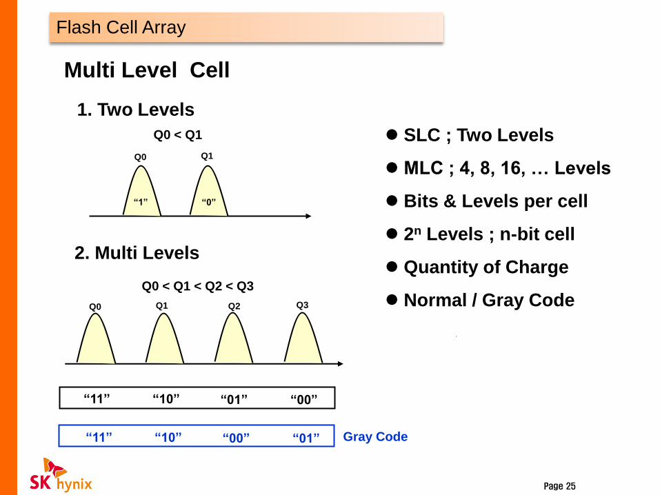
Multi Level Cell
SLC ; Two Levels
MLC ; 4, 8, 16, … Levels
Bits & Levels per cell
2n Levels ; n-bit cell
Quantity of Charge
Normal / Gray Code
“1” “0”
Q0 Q1
Q0 < Q1
“11” “10” “01” “00”
Q0 Q1 Q2 Q3
Q0 < Q1 < Q2 < Q3
1. Two Levels
2. Multi Levels
“11” “10” “00” “01” Gray Code
Flash Cell Array
Page 25

NOR/NAND MLC Cell Vth Distribution
Cell VTH
# of Bits
“11” “10” “01” “00”
Read0 Read1 Read2
program
erase
Erase Cell
PGM Cell
NOR
Cell VTH
“11” “10” “00” “01”
Read0 Read1 Read2
erase
Erase Cell
PGM Cell
NAND
0V
0V
program
Flash Cell Array
Page 26

Read Operation
NOR NAND
Selected
B/L=0.8V
Sel. W/L
(5V)
Unsel.W/L
(0V)
on off
Unselected
B/L=0V
S/A S/A
3V 7V 9V
“1” Cell “0” Cell
1V
5V
Current
“0” Cell
“1” Cell
~ 0uA
~ 40uA
-1V 1V 3V
“1” Cell “0” Cell
Current
“0” Cell
“1” Cell
~ 0uA
~ 1.2uA
B/L 0V
DSL
(4.5V)
Unsel. W/L
(4.5V)
Sel. W/L(0V)
Unsel. W/L
(4.5V)
SSL
(4.5V)
B/L 1V
“0” Cell “1” Cell
Page 27
Flash Cell Structure

Program Operation
NOR NAND
CHEI (Channel Hot Electron Injection) FN Tunneling
Selected
B/L=5V
Sel. W/L
(9V)
Unsel.W/L
(0V)
on off
Unselected
B/L=0V
S/A S/A 3V 6V 8V
“1” Cell “0” Cell
1V
4.5V
CG ONO
n+ n+
5V
9V
e
0V
p-well
0V
n-well
p-sub
B/L = 0V
DSL
(Vcc)
Unsel. W/L
(10V)
Sel. W/L
(18V)
Unsel. W/L
(10V)
SSL(0V)
B/L= Vcc
-1V 1V 3V
“1” Cell “0” Cell
CG ONO
n+ n+
18V
e e
p-well
0V
n-well
p-sub
SL=Vcc
“0” data “1” data
Page 28
Flash Cell Structure

Erase Operation
NOR NAND
FN Tunneling FN Tunneling
3V 6V 8V
“1” Cell “0” Cell
1V
4.5V
Source
(Float)
B/L = Float
W/L
(-8V)
Sector(64Kbytes) Erase CG ONO
n+ n+
float
-7,5V
e float e
8V
p-well
n-well
p-sub(0v)
-1V 1V 3V
“1” Cell “0” Cell
CG ONO
n+ n+
0V
e e
20V
p-well
n-well
p-sub(0v)
Block(16Kbytes) Erase
B/L = Float
W/L(0V)
DSL=Float
SSL=Float
W/L(0V)
W/L(0V)
SL=Float
float float
Page 29
Flash Cell Structure

4. Reliability

in 20123E/W Cycling
Write/Erase Cycle Endurance
- Flash memory cell이 허용할수 있는 Program/Erase횟수
Number of bits
Vth (Threshold Voltage)
Number of bits
Vth (Threshold Voltage)
Erase/Write
cycling
Erase cell Program cell Program cell Erase cell Control Gate
Floating Gate
Tunnel
Oxide
Interface trapping
Tox trapping
.Tunnel oxide에 electron이 trap되는 현상으로 인하여
E/W cycling의 횟수 제한이 생김
. Vt가 증가하는 현상으로 나타남
E/W Cycling
Page 31

in 20123Data Retention
Control Gate
Floating Gate
Tunnel
Oxide
Electron
Detrapping
Stress Induce
Leakage Current
Data retention
- Cell내에 저장된 Data가 일정시간 유지되는 특성
-3 -1 1 3
ON OFF
0
. Nand에서는 Vth 저하로 나타남.
. Cycling을 하여 발생한 Ox Trap or
Interface Trap이 감소하면 나타나는 것이 Major임
After Aging(Bake)
Data Retention
Page 32

Widening factor of Distribution
Page 33
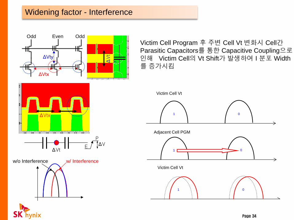
Widening factor - Interference
Page 34
w/o Interference w/ Interference
ΔVt
y ΔVtx
ΔVtx
ΔVty
Even Odd Odd
ΔV E
P
ΔVt
Victim Cell Program 후 주변 Cell Vt 변화시 Cell간
Parasitic Capacitors를 통한 Capacitive Coupling으로
인해 Victim Cell의 Vt Shift가 발생하여 I 분포 Width
를 증가시킴
1 0
Victim Cell Vt
1 0
Victim Cell Vt
1
Adjacent Cell PGM
0
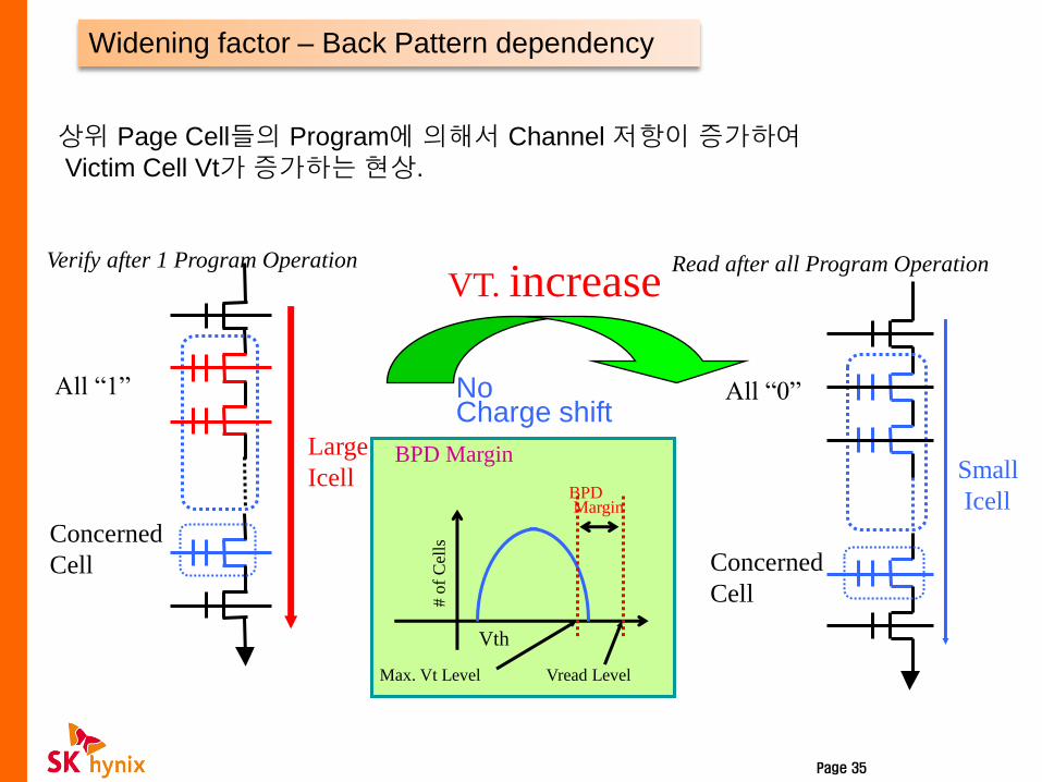
Widening factor – Back Pattern dependency
Page 35
상위 Page Cell들의 Program에 의해서 Channel 저항이 증가하여
Victim Cell Vt가 증가하는 현상.
Large
Icell
All “1”
Concerned
Cell
Verify after 1 Program Operation
Concerned
Cell
Small
Icell
All “0”
Read after all Program Operation VT. increase
No Charge shift
# o
f C
ells
Max. Vt Level
Vth
Vread Level
BPD Margin
BPD Margin

Reliability – Worsening factor
R2 R3 R1 Vread
Tech Shrink에 따른 Worsening factor들의 증가로
, Distribution Width가 증가해서 Read선에 대한 Margin이 없어짐.
=> Reliability 특성을 악화시킴
After cycling Fresh After Aging
Reliability – Worsening factor
Page 36

Reliability – Worsening factor
Tech Shrink에 따라 기하급수적으로 증가함
60 50 40 30 20200
400
600
800
1000
1200
1400
Inte
rfere
nce V
t sh
ift
(V)
Tech. node (nm)
shrink factor
Algo. + EFH
C.R + ER VT
Low-K or HVP
60 50 40 30 20
100
1000
AP
C (
mV
)Tech. node (nm)
shrink factor
D - Pgm
Poly Grain
P1 interface treat
Reliability – Worsening factor
Page 37

Flash Controller
Nand Flash
Co
ntro
ller
Host
Flash Card
Data
Data
Data
D
ata
Host Interface
File management
Wear leveling
Error Correction
Flash Card
Controller가 하는 일
Flash memory final Reliability
= Flash cell Reliability + Error Correction (Controller에서)
Flash Controller
Page 38

ECC (Error Correction Code)
Nand
Flash
Co
ntro
ller
Host
Flash Card
Da
ta
ECC En coded Data
Data
De
co
de
d D
ata
Flash memory의 입출력 Data를 Controller에서
ECC처리를 함으로써, Flash cell의 쓰기/읽기 오류
보정한다.
3xn
m 2xn
m
1xn
m
24bits 40bits
60bits
# o
f EC
C b
it( bits
/1K
B)
39
ECC(Error correction code)
Page 39

Wear leveling
Search Erase Count↓Block
Change 2 Blocks
Wear-Level End
Free Log Block Erase
Count↑
N
Y
Wear-Level Start
54
Plane 1
54
Plane 0
Chip
102 102
63 63
34 34
88 88
72 72
각 Block의 Program/Erase Count 관리를 통한 특정 Block의 집중적인 사용 회피
Erase Count를 통해 전 Block이 균일한 Program/Erase Count를 갖도록 관리.
“Erase Count가 높다?” 의 판단 기준
모든 Data Block의 Erase Count의 평균값(AVG) + Wear-Level Threshold 보다 큰 Block
AVG
Threshold
각 Block Erase count Wear leveling flow
Wear leveling
Page 40