
Hybrid CMOS/magnetic process design kit and application to the design of high-performances...
6
Hybrid CMOS/Magnetic Process Design Kit and application to the design of high-performances non-volatile logic circuits Invited Paper Guillaume PRENAT, Bernard DIENY and Jean-Pierre NOZIERES Spintec, CEA/INAC 17, rue des Martyrs 38054, Grenoble, France Email: [email protected] Gregory DiPendina and Kholdoun TORKI CMP, CNRS 46, avenue Felix Viallet 38031, Grenoble, France Email: [email protected] Abstract—Spintronics (or spin-electronics) is a continuously expending area of research and development at the merge between magnetism and electronics. It aims at taking advantage of the quantum characteristic of the electrons, i.e. its spin, to create new functionalities and new devices. Spintronic devices comprise magnetic layers which serve as spin polarizers or ana- lyzers separated by non-magnetic layers through which the spin- polarized electrons are transmitted. Typically, they rely on the Magneto Resistive (MR) effects, which consists in a dependence of the electrical resistance upon the magnetic configuration. These devices can be used to conceive innovative non-volatile memories, high-perfomances logic circuits, RF oscillators or field/current sensors. This paper describes a full Magnetic Process Design Kit (MPDK) allowing to efficiently design such CMOS/magnetic hybrid circuits. The latter can help circumventing some of the limits of CMOS-only microelectronics. I. I NTRODUCTION Magnetic Tunnel Junctions (MTJs) are well known as the basic elements of Magnetic Random Access Memories (MRAM) ([1]), a new kind of non-volatile memory which combines high writing/reading speed, low-power consump- tion, density, hardness to radiations and endurance. Due to this unique set of performances, MTJs can also be used in logic circuits. Although their intrinsic non-volatility naturally encourage to use them in memories, they can also be used to intrinsically mix memory and logic parts of the circuits to push forward the limits of CMOS microelectronics and allow new functionalities. To evaluate the performances of such hybrid circuits, it is necessary to be able to integrate these new devices in classical design suites. At transistor level, the design of a logic circuit requires a model of the electrical behavior of the components and a set of tools to draw and check the layout of the circuit before manufacturing. At higher level, standard cells are required to allow automatic design of a circuit from a Hardware Description Langage (HDL) description. In the first part of this article, we will present the hybrid Magnetic CMOS/Technology. Then, we will describe how mixing CMOS and magnetic devices can result in innovative and high-performances non-volatile logic circuits. At the end, we will present a full Process Design Kit for the CMOS/magnetic technology to design such circuits. II. DEVICE AND TECHNOLOGY A. Magnetic Tunnel Junctions MTJs (Fig.1) are nanostructures composed of two Ferro- Magnetic (FM) layers separated by an insulating layer. The magnetization of one layer, called Reference Layer (RL) is pinned in a fixed direction and acts as a reference, while the magnetization of the second one, called Storage Layer (SL) can typically be switched between two stable directions, Par- allel (P) or AntiParallel (AP) to the magnetization of the RL. According to the relative orientations of the magnetizations of the SL and the RL, the electric resistance of the MTJ changes, with an hysteretic behavior: the resistance in the AP state is larger than in the P state. Today, most MRAM technologies are based on 1 MTJ-1 transistor cell arrays (1 MTJ to store information and 1 selection transistor, ([2],[3]). To read the stored data, a current flows through the MTJ and is typically compared to a reference current to determine the resistance of the MTJ and thereby the logical stored data. Writing the MTJ can be performed in different manners, using either an external magnetic field or a spin-polarized current. The first writing technique, called FIMS for Field Induced Magnetic Switching, consists in using external magnetic fields to control the magnetization of the SL. Two perpendicular current lines are used to generate the write field: the word and bit lines (Fig.2(a)). Only the MTJ at the crossing of the two lines can be written. This approach suffers from selectivity problems because, due to process variations, the field gener- ated by a single line can sometimes write a MTJ (half selected instability). In order to circumvent the selectivity problems in this writing scheme, another approach was proposed by
-
Upload
independent -
Category
Documents
-
view
1 -
download
0
Transcript of Hybrid CMOS/magnetic process design kit and application to the design of high-performances...

Hybrid CMOS/Magnetic Process Design Kit andapplication to the design of high-performances
non-volatile logic circuitsInvited Paper
Guillaume PRENAT,Bernard DIENY
and Jean-Pierre NOZIERESSpintec, CEA/INAC17, rue des Martyrs
38054, Grenoble, FranceEmail: [email protected]
Gregory DiPendinaand Kholdoun TORKI
CMP, CNRS46, avenue Felix Viallet38031, Grenoble, France
Email: [email protected]
Abstract—Spintronics (or spin-electronics) is a continuouslyexpending area of research and development at the mergebetween magnetism and electronics. It aims at taking advantageof the quantum characteristic of the electrons, i.e. its spin, tocreate new functionalities and new devices. Spintronic devicescomprise magnetic layers which serve as spin polarizers or ana-lyzers separated by non-magnetic layers through which the spin-polarized electrons are transmitted. Typically, they rely on theMagneto Resistive (MR) effects, which consists in a dependence ofthe electrical resistance upon the magnetic configuration. Thesedevices can be used to conceive innovative non-volatile memories,high-perfomances logic circuits, RF oscillators or field/currentsensors. This paper describes a full Magnetic Process DesignKit (MPDK) allowing to efficiently design such CMOS/magnetichybrid circuits. The latter can help circumventing some of thelimits of CMOS-only microelectronics.
I. INTRODUCTION
Magnetic Tunnel Junctions (MTJs) are well known asthe basic elements of Magnetic Random Access Memories(MRAM) ([1]), a new kind of non-volatile memory whichcombines high writing/reading speed, low-power consump-tion, density, hardness to radiations and endurance. Due tothis unique set of performances, MTJs can also be used inlogic circuits. Although their intrinsic non-volatility naturallyencourage to use them in memories, they can also be usedto intrinsically mix memory and logic parts of the circuitsto push forward the limits of CMOS microelectronics andallow new functionalities. To evaluate the performances ofsuch hybrid circuits, it is necessary to be able to integratethese new devices in classical design suites. At transistorlevel, the design of a logic circuit requires a model of theelectrical behavior of the components and a set of tools to drawand check the layout of the circuit before manufacturing. Athigher level, standard cells are required to allow automaticdesign of a circuit from a Hardware Description Langage(HDL) description. In the first part of this article, we willpresent the hybrid Magnetic CMOS/Technology. Then, we
will describe how mixing CMOS and magnetic devices canresult in innovative and high-performances non-volatile logiccircuits. At the end, we will present a full Process Design Kitfor the CMOS/magnetic technology to design such circuits.
II. DEVICE AND TECHNOLOGY
A. Magnetic Tunnel Junctions
MTJs (Fig.1) are nanostructures composed of two Ferro-Magnetic (FM) layers separated by an insulating layer. Themagnetization of one layer, called Reference Layer (RL) ispinned in a fixed direction and acts as a reference, while themagnetization of the second one, called Storage Layer (SL)can typically be switched between two stable directions, Par-allel (P) or AntiParallel (AP) to the magnetization of the RL.According to the relative orientations of the magnetizations ofthe SL and the RL, the electric resistance of the MTJ changes,with an hysteretic behavior: the resistance in the AP state islarger than in the P state. Today, most MRAM technologiesare based on 1 MTJ-1 transistor cell arrays (1 MTJ to storeinformation and 1 selection transistor, ([2],[3]). To read thestored data, a current flows through the MTJ and is typicallycompared to a reference current to determine the resistanceof the MTJ and thereby the logical stored data. Writing theMTJ can be performed in different manners, using either anexternal magnetic field or a spin-polarized current.
The first writing technique, called FIMS for Field InducedMagnetic Switching, consists in using external magnetic fieldsto control the magnetization of the SL. Two perpendicularcurrent lines are used to generate the write field: the word andbit lines (Fig.2(a)). Only the MTJ at the crossing of the twolines can be written. This approach suffers from selectivityproblems because, due to process variations, the field gener-ated by a single line can sometimes write a MTJ (half selectedinstability). In order to circumvent the selectivity problemsin this writing scheme, another approach was proposed by
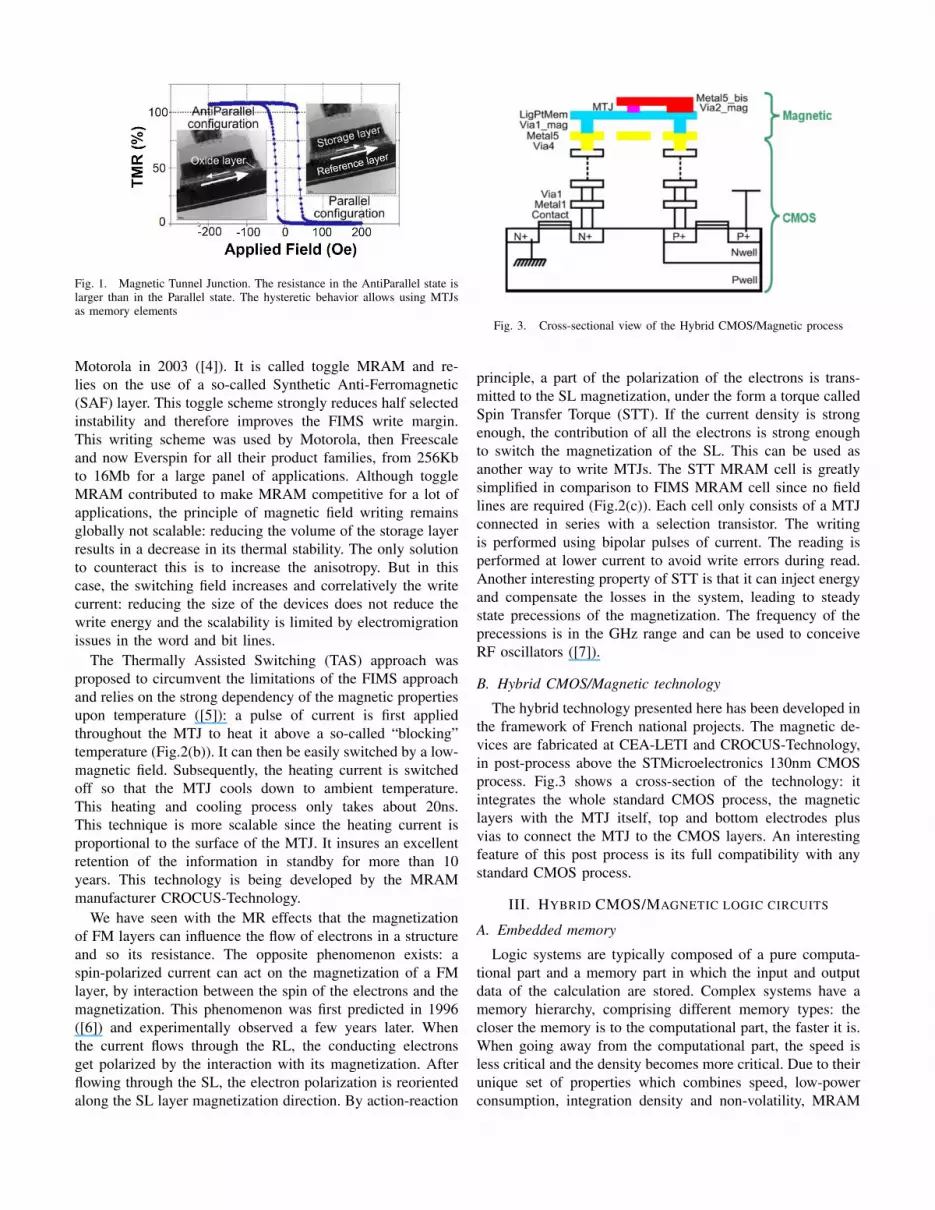
Fig. 1. Magnetic Tunnel Junction. The resistance in the AntiParallel state islarger than in the Parallel state. The hysteretic behavior allows using MTJsas memory elements
Motorola in 2003 ([4]). It is called toggle MRAM and re-lies on the use of a so-called Synthetic Anti-Ferromagnetic(SAF) layer. This toggle scheme strongly reduces half selectedinstability and therefore improves the FIMS write margin.This writing scheme was used by Motorola, then Freescaleand now Everspin for all their product families, from 256Kbto 16Mb for a large panel of applications. Although toggleMRAM contributed to make MRAM competitive for a lot ofapplications, the principle of magnetic field writing remainsglobally not scalable: reducing the volume of the storage layerresults in a decrease in its thermal stability. The only solutionto counteract this is to increase the anisotropy. But in thiscase, the switching field increases and correlatively the writecurrent: reducing the size of the devices does not reduce thewrite energy and the scalability is limited by electromigrationissues in the word and bit lines.
The Thermally Assisted Switching (TAS) approach wasproposed to circumvent the limitations of the FIMS approachand relies on the strong dependency of the magnetic propertiesupon temperature ([5]): a pulse of current is first appliedthroughout the MTJ to heat it above a so-called “blocking”temperature (Fig.2(b)). It can then be easily switched by a low-magnetic field. Subsequently, the heating current is switchedoff so that the MTJ cools down to ambient temperature.This heating and cooling process only takes about 20ns.This technique is more scalable since the heating current isproportional to the surface of the MTJ. It insures an excellentretention of the information in standby for more than 10years. This technology is being developed by the MRAMmanufacturer CROCUS-Technology.
We have seen with the MR effects that the magnetizationof FM layers can influence the flow of electrons in a structureand so its resistance. The opposite phenomenon exists: aspin-polarized current can act on the magnetization of a FMlayer, by interaction between the spin of the electrons and themagnetization. This phenomenon was first predicted in 1996([6]) and experimentally observed a few years later. Whenthe current flows through the RL, the conducting electronsget polarized by the interaction with its magnetization. Afterflowing through the SL, the electron polarization is reorientedalong the SL layer magnetization direction. By action-reaction
Fig. 3. Cross-sectional view of the Hybrid CMOS/Magnetic process
principle, a part of the polarization of the electrons is trans-mitted to the SL magnetization, under the form a torque calledSpin Transfer Torque (STT). If the current density is strongenough, the contribution of all the electrons is strong enoughto switch the magnetization of the SL. This can be used asanother way to write MTJs. The STT MRAM cell is greatlysimplified in comparison to FIMS MRAM cell since no fieldlines are required (Fig.2(c)). Each cell only consists of a MTJconnected in series with a selection transistor. The writingis performed using bipolar pulses of current. The reading isperformed at lower current to avoid write errors during read.Another interesting property of STT is that it can inject energyand compensate the losses in the system, leading to steadystate precessions of the magnetization. The frequency of theprecessions is in the GHz range and can be used to conceiveRF oscillators ([7]).
B. Hybrid CMOS/Magnetic technology
The hybrid technology presented here has been developed inthe framework of French national projects. The magnetic de-vices are fabricated at CEA-LETI and CROCUS-Technology,in post-process above the STMicroelectronics 130nm CMOSprocess. Fig.3 shows a cross-section of the technology: itintegrates the whole standard CMOS process, the magneticlayers with the MTJ itself, top and bottom electrodes plusvias to connect the MTJ to the CMOS layers. An interestingfeature of this post process is its full compatibility with anystandard CMOS process.
III. HYBRID CMOS/MAGNETIC LOGIC CIRCUITS
A. Embedded memory
Logic systems are typically composed of a pure computa-tional part and a memory part in which the input and outputdata of the calculation are stored. Complex systems have amemory hierarchy, comprising different memory types: thecloser the memory is to the computational part, the faster it is.When going away from the computational part, the speed isless critical and the density becomes more critical. Due to theirunique set of properties which combines speed, low-powerconsumption, integration density and non-volatility, MRAM

Fig. 2. (a) FIMS-based MRAM cell, (b) TAS-based MRAM cell and (c) STT-based MRAM cell)
could replace parts of the memory hierarchy. As a result,the architecture of processors could be redesigned to takeadvantage of MTJs to improve performances, in particular interms of power consumption and related heating issues.
B. Non-volatile SRAM
The operating frequency of Flip-Flops or low-level cacheis larger than 1GHz. Classical MRAM cannot reach suchspeeds. However, beside classical 1T-1MTJ structure, non-volatile SRAM was proposed, called Black and Das cell ([8],Fig.4). This structure looks like a classical SRAM latch, withan additional pair of MTJs, a set of transistors to write theMTJs (for example transistors to produce the heating currentin TAS technology) and an AutoZero (AZ) transistor. Twologic values are stored in this latch: an information in thelatch itself (Q and Q bar), which is the information availableand an information stored in a differential way in the MTJs(one MTJ is Parallel while the other is AntiParallel). Whilethe AZ transistor is open, the MTJs have no influence andthe cell works as a standard SRAM, with the same speed.When the AZ transistor is closed, the latch is shortened, andthe difference of resistance in the magnetic branch unbalancesit. When the AZ signal is removed, the latch switches to astate corresponding to the value stored in the MTJs. In theAZ operation, the latch operates as a sense amplifier to readthe MTJs state. This cell can be used for example to backupthe active data in the magnetic part and to restore it at anytime within a few hundreds of picoseconds. Combined with aclassical SRAM latch, this cell can be used to create a Non-Volatile Flip-Flop (NVFF, [9], [10]).
C. Field Programmable Gate Array
Field Programmable Gate Arrays (FPGA) are essentiallycomposed of memory. They are currently based on SRAMand/or Flash memory. SRAM-based FPGA are fast to program,but less dense and require an additional non-volatile memory(typically Flash) to permanently store information when pow-ered off. Fully Flash-based FPGA are denser, but the writ-ing time and energy consumption prevents them from beingused for reconfigurable computing for example. MRAM-basedFPGA could combine the advantages of the two approaches toobtain a really fast non-volatile FPGA. In such a FPGA, a shiftregister based on the non-volatile SRAM Flip-Flop presentedpreviously could be used for example to load the configuration
Fig. 4. Non-volatile SRAM cell
once in serial, then to back it up in the magnetic part, so thatit can be loaded in less than 1ns at startup (or reloaded at anytime) in case of failure ([10]). The use of the non-volatility alsoallows new functionalities. Shadowed reconfiguration consistsin changing the functionality of a circuit without affecting itsongoing operation. This is eased by the use of non-volatileSRAM cells since writing the magnetic configuration does notaffect the value stored in the latch. In addition, by using severalpairs of MTJs instead of one and a tree of selection transistorsseveral configurations could be chosen (multicontext, [10]).
D. Low-power non-volatile logic circuits
In advanced CMOS technologies, the drastic reduction inthe size of devices results in a strong increase of the powerconsumption, especially of the standby power consumptiondue to leakage. This also results in heating and reliabilityissues. Several techniques are being used to limit the powerconsumption at the technology level (SOI, HiK gates [11]),at the design level (using Multi or Variable Threshold MOStransistors [12]) or at the system level (clock gating, powergating, Dynamic Voltage and Frequency Scaling). Powergating consists in cutting off the power supply of unusedblocks to avoid leakage and thereby limit the standby powerconsumption. To avoid loosing the active data, it is possible tostore them in distant very low-leakage or non-volatile register(resulting in delays an dynamic power consumption). It is alsopossible to only reduce the supply voltage in the retentionphase (but in this case a small leakage remains). Using non-
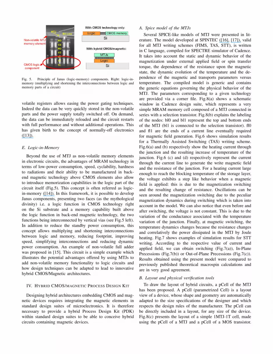
Fig. 5. Principle of Janus (logic-memory) components. Right: logic-in-memory (multiplying and shortening the interconnections between logic andmemory parts of a circuit)
volatile registers allows easing the power gating techniques.Indeed the data can be very quickly stored in the non-volatileparts and the power supply totally switched off. On demand,the data can be immediately reloaded and the circuit restartswith full performance and without additional operations. Thishas given birth to the concept of normally-off electronics([13]).
E. Logic-in-Memory
Beyond the use of MTJ as non-volatile memory elementsin electronic circuits, the advantages of MRAM technology interms of low-power consumption, speed, cyclability, hardnessto radiations and their ability to be manufactured in back-end magnetic technology above CMOS elements also allowto introduce memorization capabilities in the logic part of thecircuit itself (Fig.5). This concept is often referred as logic-in-memory ([14]). In this framework, it is possible to developJanus components, presenting two faces (as the mythologicaldivinity) i.e. a logic function in CMOS technology righton the Si substrate and a memory capability built abovethe logic function in back-end magnetic technology, the twofunctions being interconnected by vertical vias (see Fig.5 left).In addition to reduce the standby power consumption, thisconcept allows multiplying and shortening interconnectionsbetween logic and memory, reducing footprint, improvingspeed, simplifying interconnections and reducing dynamicpower consumption. An example of non-volatile full adderwas proposed in [15]. This circuit is a simple example whichillustrates the potential advantages offered by using MTJs toadd non-volatile memory functionality to logic circuits andhow design techniques can be adapted to lead to innovativehybrid CMOS/Magnetic architectures.
IV. HYBRID CMOS/MAGNETIC PROCESS DESIGN KIT
Designing hybrid architectures embedding CMOS and mag-netic devices requires integrating the magnetic elements instandard design suites of microelectronics. It is thereforenecessary to provide a hybrid Process Design Kit (PDK)within standard design suites to be able to conceive hybridcircuits containing magnetic devices.
A. Spice model of the MTJs
Several SPICE-like models of MTJ were presented in lit-erature. The model developed at SPINTEC ([16], [17]), validfor all MTJ writing schemes (FIMS, TAS, STT), is writtenin C language, compiled for SPECTRE simulator of Cadence.It takes into account the static and dynamic behavior of themagnetization under external applied field or spin transfertorque, the dependence of the resistance upon the magneticstate, the dynamic evolution of the temperature and the de-pendence of the magnetic and transports parameters versustemperature. The compiled model is generic and containsthe generic equations governing the physical behavior of theMTJ. The parameters corresponding to a given technologyare provided via a corner file. Fig.8(a) shows a schematicwindow in Cadence design suite, which represents a verysimple MRAM memory cell composed of a MTJ connected inseries with a selection transistor. Fig.8(b) explains the labelingof the nodes: bl0 and bl1 represent the top and bottom endsof the MTJ (bl1 is connected to the selection transistor). fl0and fl1 are the ends of a current line eventually requiredfor magnetic field generation. Fig.6 shows simulation resultsfor a Thermally Assisted Switching (TAS) writing scheme.Fig.6(a) and (b) respectively show the heating current throughthe junction and the resulting increase of temperature of thejunction. Fig.6 (c) and (d) respectively represent the currentthrough the current line to generate the write magnetic fieldand the resistance of the junction. For a heating current largeenough to reach the blocking temperature of the storage layer,the voltage exhibits a step like behavior when a magneticfield is applied: this is due to the magnetization switchingand the resulting change of resistance. Oscillations can beseen around the magnetization switching due to the peculiarmagnetization dynamics during switching which is taken intoaccount in the model. We can also notice that even before andafter switching, the voltage is not constant. This is due to thevariation of the conductance associated with the temperaturevariation of the junction. Finally, at magnetic switching, thetemperature dynamics changes because the resistance changesand correlatively the power dissipated in the MTJ by Jouleheating. Fig.7 shows examples of simulation results for STTwriting. According to the respective value of current andapplied field, we can obtain switching (Fig.7(a)), In-PlanePrecessions (Fig.7(b)) or Out-of-Plane Precessions (Fig.7(c)).Results obtained using the present model were compared topreviously published theoretical macrospin calculations andare in very good agreement.
B. Layout and physical verification tools
To draw the layout of hybrid circuits, a pCell of the MTJhas been proposed. A pCell (parametrized Cell) is a layoutview of a device, whose shape and geometry are automaticallyadapted to the size specifications of the designer and whichrespects the design rules of the manufacturer. The pCell canbe directly included in a layout, for any size of the device.Fig.8(c) presents the layout of a simple 1MTJ-1T cell, madeusing the pCell of a MTJ and a pCell of a MOS transistor.

(a) (b) (c)
Fig. 8. (a) schematic under CADENCE of a simple MRAM memory cell composed of a MTJ realized in back-end magnetic process above a selectiontransistor, (b)explanation of the labeling of the nodes and (c) corresponding layout with the pCell of the MTJ and the pCell of the transistor)
Fig. 6. Simulation results for a TAS memory cell. Heating current (a),resulting increase of temperature (b), current used to generate the writingmagnetic field (c) and resistance of the MTJ (d)
Fig. 7. Precessionnal modes of the magnetization for a MTJ submittedto the combined influence of the spin transfer torque generated by the spinpolarized current flowing through the MTJ with that of an external magneticfield. Depending of the values of current and field, various regimes can beobserved: Switching of the magnetization (a), In Plane Precessions (b) andOut of Plane Precessions (c)
The technology parameters corresponding to the magneticback-end have been integrated to the technology files toallow physical verifications: verification of the design rules(Design Rules Checking, DRC), identification of the devices,interconnections and parasitics from the layout (extraction)and verification of the correspondence between the simulatedschematic and the layout (Layout Versus Schematic, LVS).
C. Standard cells, digital design tools
A complex digital architecture is generally synthesizedautomatically from elementary logic functions called stan-dard cells. Several standard cells of Non-Volatile Flip-Flops(NVFF) based on the Black and Das principle have beendesigned, characterized and included in a standard digitaldesign flow in the framework of a collaboration between CMPand Spintec. In order to be able to run digital simulationsfor advanced and complex designs, a full Verilog descriptionof the NVFF has been developed. It takes into account thebehavior and also the timing checks for the MTJs heatingduration, writing and reading. To design non volatile blocksusing the innovative flip-flop standard cell described above,the synthesis uses a specific library containing only registersmade of CMOS and MTJs. The connections between all themagnetic signals are defined in the HDL description whereall these signals need to be declared and interconnected tomanage the MTJ writing and reading. As a consequence, thenetlist extracted from the synthesis includes the NVFF andboth connections of CMOS and magnetic signals. The abstractview of the NVFF is given in order to place and route a fullblock composed of standard cells, using standard tools. Tocomplete final simulations, an Standard Delay Format (SDF)file including the NVFF internal timings can be extracted fromthe placed and routed layout to back annotate the netlist to runmore accurate simulations.
V. CONCLUSIONS
Hybrid CMOS/Magnetic circuits appear to be good candi-dates to circumvent the limits of classical CMOS electronics.The hybrid CMOS/magnetic technology is new and there-fore is not as mature as CMOS technology. However steadyprogress are observed in terms of MTJ performances andprocess variations thanks to all the ongoing R&D effort onMRAM. Since the technology is very similar for MRAM andhybrid CMOS/MTJ non-volatile logic, these progresses willdirectly benefit to this field. When this hybrid technology isstabilized, characterization results with good statistics will beprovided to improve the accuracy of the models and to stan-dardize the tools. Nevertheless, several circuits have already

been fabricated yielding very encouraging results. Moreover,the writing schemes based on Spin Transfer Torque or Ther-mal Assistance are very scalable, since the switching of themagnetic state is driven by the current density. The advantagesof mixing MTJs with CMOS devices should become more andmore obvious with advanced technologies. Of course, this newtechnology can be used together with other design techniquesto improve the performance of electronic circuits, especially interms of power consumption. Some research has to be carriedout to see how these different techniques can be combined.In particular, some of these techniques are efficient at the fullsystem level. It is then necessary to evaluate the opportunitiesprovided by this technology for complete systems and incomparison or combination with existing techniques and foradvanced technologies.
REFERENCES
[1] S.Tehrani, “Magnetoresistive random access memory using magnetictunnel junctions,” proceedings of IEEE, vol. 91, no. 5, pp. 3703–3714,May 2003.
[2] S. Tehrani, B.Engel, J. Slaughter, E. Chen, M. DeHerrera, M. Durlam,P. Naji, R. Whig, J. Janesky, and J. Calder, “Recent developmentsin magnetic tunnel junction mram,,” IEEE Transactions on magnetics,vol. 36, no. 5, p. 2752, 2000.
[3] R.Scheuerlein, W. Gallagher, S. Parkin, A. Lee, S. Ray, R. Robertazzi,and W. Reohr, “a 10ns read and write non-volatile mmeory array using amagnetic tunnel junction and fet switch in each cell,” Digest of technicalpapers, IEEE International Solid State Circuits Conference, vol. 128,2000.
[4] L. Savtchenko, B. Engel, N. Rizzo, M. Deherrera, and J. Janesky,“Method of writing to scalable magnetoresistance random access mem-ory element,” US6545906.
[5] I.L.Prejbeanu, W. Kula, K. Ounadjela, R. Sousa, O. Redon, B. Dieny, andJ. Nozieres, “Thermally assisted switching in exchange-biased storagelayer magnetic tunnel junctions,” IEEE Transactions on Magnetics,vol. 40, no. 4, 2004.
[6] J. Slonczewski, “Currents and torques in metallic magnetic multilayers,”J.Magn.Magn.Mater., vol. 159, no. 1, 1996.
[7] S.I.Kiselev, J. andI.N.Krivorotov, N.C.Emley, R.J.Schoelkopf,R.A.Buhrman, and D.C.Ralph, “Microwave oscillations of a nanomagnetdriven by a spin-polarized current,” Nature, vol. 425, 2003.
[8] W. Black and B. Das, “Programmable logic using giant-magneto-resistance and spindependent tunneling devices,” J. Appl. Phys., vol. 87,no. 9, pp. 6674–6679, 2000.
[9] W.Zhao, E. Belhaire, V. Javerliac, C.Chappert, and B. Dieny, “A non-volatile flip-flop in magnetic fpga chip,” in IEEE International Designand Test of Integrated Systems conference, Tunisia, 2006.
[10] Y.Guillemenet, L. Torres, G.Sassatelli, and N. Bruchon, “On the useof magnetic rams in field-programmable gate arrays,” Int. Journ. ofReconfigurable Computing, vol. 2008, 2008.
[11] M.Caymax, S. Gendt, W.Vandervorst, M.Heyns, H.Bender, R.Carter,T.Conard, R.Degraeve, G.Groeseneken, S.Kubicek, G.Lujan,L.Pantisano, J.Petry, E.Rohr, S. elshocht, C.Zhao, E.Cartier, J.Chen,V.Cosnier, S. annd V.Kaushik, A.Kerber, J.Kluth, S.Lin, W.Tsai,E.Young, and Y.Manabe, “Issues, achievements and challenges towardsintegration of high-k dielectrics,” Int. Journ. of High Speed Electronicsand Systems, vol. 12, no. 2, pp. 295–304, 2008.
[12] S.Mutoh, T.Douseki, Y.Matsuya, T. Aoki, S. Shigematsu, andJ.Yamada, “1-v power supply high-speed digital circuit technology withmultithreshold-voltage cmos,” IEEE Journal of Solid State Circuits,vol. 30, no. 8, pp. 847–854, 1995.
[13] T.Kawahara, “Scalable spin-transfer torque ram technology fornormally-off computing,” Design and Test of Computers, vol. 28, no. 1,2010.
[14] A.Mochizuki, H. Kimura, M. Ibuki, and T.Hanyu, “Tmr-based logic-in-memory circuit for low-power vlsi,” IEICE Transactions on Funda-mentals of Electronics, Communications and Computer Sciences, vol.E88-A, no. 6, pp. 1408–1415, 2005.
[15] S.Matsunaga, J.Hayakawa, S.Ikeda, K.Miura, H. Hasegawa, T. Endoh,H. Ohno, T., and Hanyu, “Fabrication of a non-volatile full adderbased on logic-in-memory architecture using magnetic tunnel junctions,”Applied Physics Express, vol. 1, 2008.
[16] M.ElBaraji, V. Javerliac, W.Guo, G.Prenat, and B. Dieny, “Dynamiccompact model of thermally assisted switching magnetic tunnel junc-tions,” Journal of Applied Physics, vol. 106, no. 12, p. 123906, 2009.
[17] W.Guo, G.Prenat, V. Javerliac, M.ElBaraji, N. DeMestier, C. Baraduc,and B. Dieny, “Spice modeling of magnetic tunnel junctions written byspin-transfer torque,” Journal of Physics D: Applied Physics, vol. 43,no. 21, p. 215001, 2010.