LAYOUT DESIGN OF 32-BIT BRENT KUNG ADDER (CMOS ...
52
LAYOUT DESIGN OF 32-BIT BRENT KUNG ADDER (CMOS LOGIC) By VINISH KALVA BACHELOR OF TECHNOLOGY in ELECTRONICS AND COMMUNICATION ENGINEERING Acharya Nagarjuna University Vijayawada, A.P, India Submitted to the faculty of the Graduate College of the Oklahoma State University in partial fulfillment of the requirements for the Degree of MASTER OF SCIENCE, May, 2015
-
Upload
khangminh22 -
Category
Documents
-
view
0 -
download
0
Transcript of LAYOUT DESIGN OF 32-BIT BRENT KUNG ADDER (CMOS ...

LAYOUT DESIGN OF 32-BIT BRENT KUNG
ADDER (CMOS LOGIC)
By
VINISH KALVA
BACHELOR OF TECHNOLOGY in ELECTRONICS
AND COMMUNICATION ENGINEERING
Acharya Nagarjuna University
Vijayawada, A.P, India
Submitted to the faculty of the
Graduate College of the Oklahoma State University in
partial fulfillment of the requirements for the Degree of
MASTER OF SCIENCE,
May, 2015

ii
LAYOUT DESIGN OF 32-BIT BRENT KUNG ADDER
(CMOS LOGIC)
Thesis Approved:
Johnson, Louis G., Ph.D.
Thesis Adviser
Ramakumar, R. G., Ph.D
Sheng, Weihua, Ph.D

iii
ACKNOWLEDGEMENTS
This thesis work reflects the contributions of people without whom, it would not
have been possible.
I first express my sincere thanks to our institute Oklahoma State University for
providing a wonderful platform for implementing the idea and extending the required
software. I express my whole-hearted gratitude to my guide Dr. L.G. Johnson, who with
his valuable suggestions and moral support and by providing all the resources needed,
made the job look easy and helped me in completing the project in time.
I thank my committee members Dr. R.G. Ramakumar, and Dr. Weihua Sheng
for encouraging me to do this project.
VINISH KALVA (11603851)
"Acknowledgements reflect the views of the author and are not endorsed by committee
members or Oklahoma State University."
iv
Name: VINISH KALVA
Date of Degree: May, 2015
Title of Study: LAYOUT DESIGN OF 32-BIT BRENT KUNG ADDER (CMOS
LOGIC)
Major Field: Electrical and Computer Engineering.
Abstract: Adders play a key role in the arithmetic circuits. These arithmetic circuits
perform operations like addition, subtraction, multiplication, division, parity calculation
etc. The performance of the microprocessors mainly depends upon the speed of the
response of these arithmetic operations. Apart from the arithmetic operations the adders
are also used for calculating the addresses, tables and similar operations. It is also used in
digital signal processor (DSP). As adder is the main circuit, the performance depends on
its functioning or speed. Improving its performance is the main area of research in VLSI
system design.
The conventional adders may work well for small number of bits but when the
length increases (say 32-bit, 64-bit, 128-bit and so on) the performance of the
conventional adders degrades. Thus in industries tree adders or parallel prefix adders are
used for arithmetic operations.
There are 6 types of tree adders. Here in this work the layout of 32-bit Brent Kung adder
is designed and its delay is calculated. The layouts of 16-bit Brent Kung, Sklansky,
Kogge Stone adders are also designed and their delays are compared. The critical path for
all these tree adders is computed. For designing these layouts the software used is ‘magic
layout tool’ and outputs are verified using ‘IRSIM’. Minimum transistor width (5lambda)
is used in these designs.

v
CONTENTS:
NAME PAGE NO
1. BACKGROUND 1
1.1. HALF ADDER 2
1.2. FULL ADDER 3
1.3. CARRY RIPPLE ADDER 5
1.4. CARRY SKIP ADDER 9
1.5. CARRY LOOK AHEAD ADDER 12
1.6. CARRY SELECT ADDER 12
1.7. TREE ADDERS OR PARALLEL PREFIX ADDERS 17
2. DESIGN AND IMPLEMENTATION 20
3. SOFTWARE USED 28
3.1. MAGIC 31
3.2. IRSIM 27
4. RESULT ANALYSIS 36
5. CONCLUSION AND FUTURE WORK 41
6. REFERENCES 43

vi
LIST OF FIGURES
NAME PAGE NO
Fig.1.0: Half adder 2
Fig 1.1: Full adder 3
Fig.1.3: Layout design of full adder 4
Fig.1.4: Carry ripple adder (4-bit) 5
Fig.1.5: Addition with generate and propagate logic 6
Fig.1.6: Carry ripple adder with group PG logic 8
Fig.1.7: Group PG cells 9
Fig.1.8: Carry skip adder 9
Fig.1.9: Carry skip adder group PG network 10
Fig 1.10: Carry skip adder with variable sizes of blocks 11
Fig 1.11: Carry look ahead adder 12
Fig 1.12: Carry select adder 12
Fig 1.13: Carry increment adder PG network 13
Fig 1.14: Variable length carry increment adder 14
Fig 1.15: Carry increment adder with buffers 14
Fig 1.16: 16-bit conditional sum adder 15
Fig 1.17: 16-bit Brent Kung adder 17
Fig 1.18: 16-bit Kogge Stone adder 18
Fig 1.19: 16-bit Sklansky adder 19
Fig 2.1: Block diagram of bit-wise PG logic 20
Fig 2.2: Block diagram of Grey cell 20
Fig 2.3: Block diagram of black cell 21
Fig 2.4: Layout of Inverter 22
Fig 2.5: Layout of NAND 23

vii
Fig 2.6: Layout of NOR 23
Fig 2.7: Layout of AND logic gate 24
Fig 2.8: Layout of OR logic gate 24
Fig 2.9: Layout of XOR gate 25
Fig 2.10: Layout of PG logic 25
Fig 2.11: Layout of AOI (grey cell) 26
Fig 2.12: Layout of AOI (black cell) 26
Fig 2.13: 32-bit Brent Kung adder block diagram with critical path 27
Fig 3.1: Colors of metals and layers used in magic layout tool 29
Fig 3.2: Commands used for the layers 31
Fig 4.1: IRSIM output for 16-bit Brent Kung adder 36
Fig 4.2: The critical path delay for 16-bit Brent Kung adder 37
Fig 4.3: IRSIM output of 16-bit Kogge Stone adder 37
Fig 4.4: The critical path delay for 16-bit Kogge Stone adder 38
Fig 4.5. IRSIM output of 16-bit Sklansky adder 38
Fig 4.6. The critical path delay for 16-bit Sklansky adder 39
Fig 4.7: IRSIM output for 32-bit Brent Kung adder 39
Fig 4.8: Critical path delay for 32-bit Brent Kung adder 40
Fig 5.1: Graph indicating the delays of the adders designed 42
1
CHAPTER I
BACKGROUND
In every arithmetic circuits we have arithmetic operations like addition,
subtraction, multiplication, division, parity calculation etc. But of all those an adder or a
summer is the key component in any processor or computer. Mostly these adders are not
only used in arithmetic operations but also in calculating addresses, lookup tables etc.
Addition circuits are also used in cryptography applications. Thus the speed of the
response of any DSP (digital signal processor) or a microprocessor depends on the binary
adders used in it.
Designing of an improvised adder with very good performance is the main area of
research in VLSI system design. As the conventional adders (ripple carry adders) produce
more delay, the carry look ahead adders are preferred to them. In RCA the delay is
caused due to the generation of carry. But, in CLA the carry bits are calculated before the
sum bit for one or more bits.
Parallel prefix adders are the advanced CLAs. There are different ways to generate the
carriers in these prefix adders depending on the application or requirement. Here a tree
like structure is used to increase the speed of the response. The advantage of these prefix

2
adders is the flexibility in implementing the tree structures based upon the throughput
requirements. Here the addition is represented in prefix computation form. Using these prefix
computations provides various intermediate structures within the adder. Therefore a parallel
prefix adder is designed with different set of speed, area and power depending upon the
requirement.
A binary adder is a digital circuit used to calculate the addition of numbers in electronics.
It is not only used for arithmetic operations but also used for calculation of table indices,
addresses, binary coded decimal, excess-3 etc.
Binary adders are also used for subtraction or operating on signed bit numbers by making
few changes to it. The two’s compliment or one’s compliment is used to represent the negative
sign in the subtraction and signed bit addition.
1.1. Half adder: Two single bits are added in half adder (A and B). So, the result is 0
or 1 or 2. To represent 2, two bits are required and they are called sum and carry.
The block diagram and truth table of half adder is given below.
Figure1.0 - Half adder

3
1.2. Full adder: The carry out in half adder is equivalent to a carry in to the next
stage in a multi bit adder. That is in multiple bit addition the adders are cascaded
and the carry is propagated to the next stage. So an adder receives a carry-in as
input. This is called full adder, its truth table and logic level diagram are given
below.
In full adders sometimes generate(G), propagate(P), kill(K) signals are
also used. Where G = A.B i.e. a carry out is generated irrespective of Cin. K=
~A.~B i.e. an adder kills a carry when Cout is zero irrespective of Cin. The
propagate signal P = is similar to the sum output of a full adder. The
truth table is given below with propagate, generate, kill signals.
Figure 1.1 – Full adder

4
The sum output can be represented as below
Thus the full adder is constructed as shown in the gate level diagram. Its layout
design will be as follows (CMOS technology).
Figure 1.3. Layout design of full adder.

5
1.3. Carry ripple adder: For an N-bit adder, N full adders are used. The carry-in for
a full adder is carry-out from the previous stage. Thus all the N full adders are
connected together to make it a carry ripple adder. The design of this ripple adder
is very easy and takes very less time to design. But the delay is more and the
response is relatively slow compared to other adders since at each stage the adder
should wait for the carry from the previous stage.
The speed of the propagation of the carry can be increased by using the
AND-OR-invert gates. There are faster ways to reduce the response time by
using carry-look ahead adders.
Carry-look ahead adders: This adder improves the speed of the response.
Each stage doesn’t need to wait for the carry from the previous stage. Here the
adder calculates one or more carry bits before the sum which reduces the delay in
response.
Here we group the adders and this group propagates the carry to the next
group. Let’s say there is a group with bits from i to j. It propagates carry to the
next stage if it generates carry irrespective of the carry-in to this group. It
Figure 1.4. Carry ripple adder (4-bit)

6
generates a carry if there is a carry-in to this group. As discussed earlier this
method uses the signals ‘propagate’ and ‘generate’ signals.
A carry is generated from the group if the upper portion or the lower
portion generates or the upper portion propagates a carry. The initial carry-in
should be defined i.e. Cin.
Thus we can find out the carry-out of a certain stage as Ci-1 =Gi1:0. The
addition is calculated by three stages.
a) We take the signals ‘propagate’ and ‘generate’ into
consideration.
b) By combining the P and G signals we calculate Gi-1:0 using the
above mentioned equation.
c) Then sum is calculated using the below equation.
As shown in the diagram first we calculate the ‘P’ and ‘G’ signals in
every stage. A different logic is applied in group PG logic depending on the
Figure 1.5. Addition with generate and propagate logic.
7
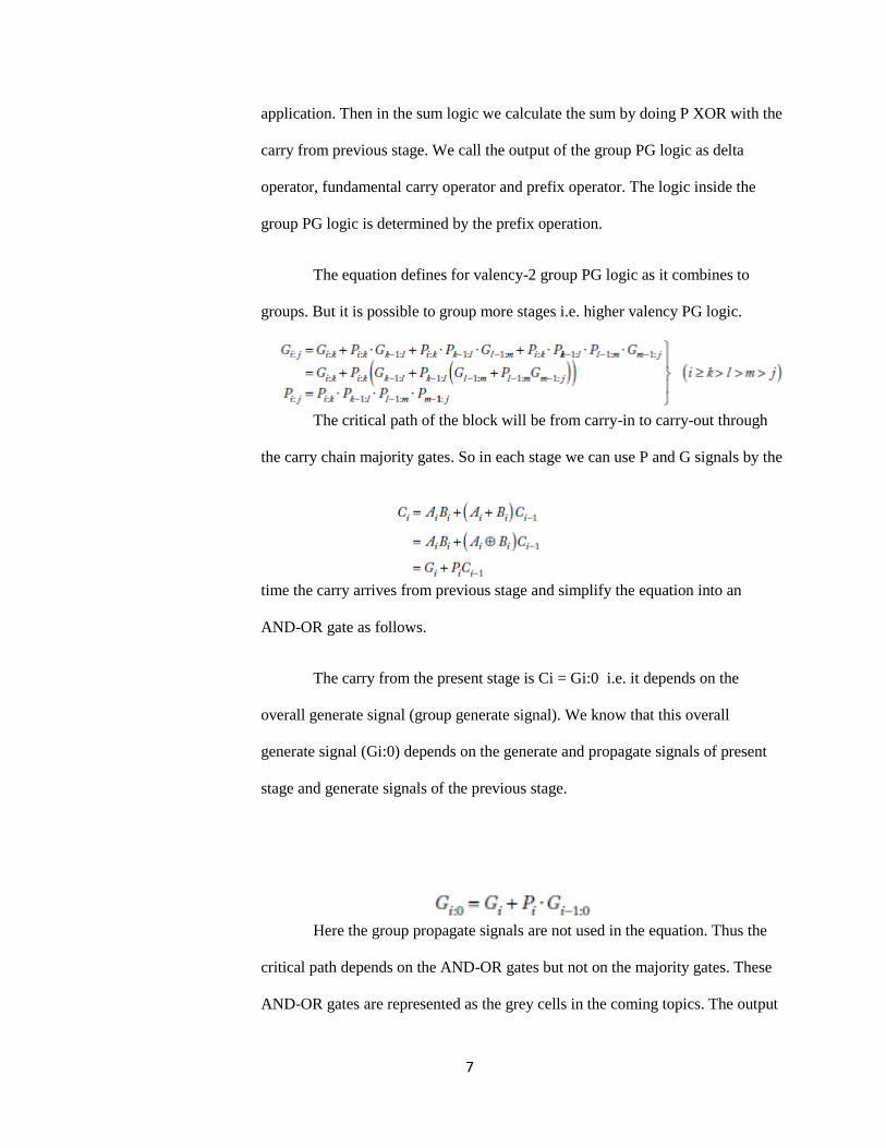
application. Then in the sum logic we calculate the sum by doing P XOR with the
carry from previous stage. We call the output of the group PG logic as delta
operator, fundamental carry operator and prefix operator. The logic inside the
group PG logic is determined by the prefix operation.
The equation defines for valency-2 group PG logic as it combines to
groups. But it is possible to group more stages i.e. higher valency PG logic.
The critical path of the block will be from carry-in to carry-out through
the carry chain majority gates. So in each stage we can use P and G signals by the
time the carry arrives from previous stage and simplify the equation into an
AND-OR gate as follows.
The carry from the present stage is Ci = Gi:0 i.e. it depends on the
overall generate signal (group generate signal). We know that this overall
generate signal (Gi:0) depends on the generate and propagate signals of present
stage and generate signals of the previous stage.
Here the group propagate signals are not used in the equation. Thus the
critical path depends on the AND-OR gates but not on the majority gates. These
AND-OR gates are represented as the grey cells in the coming topics. The output

8
of the grey cell is the group generate signal which is used to calculate the carry of
that stage.
The figure describes about the 16-bit adder with P, G signals (bitwise
PG) and grey cells (AND-OR gates). In the coming topics, different adder
architectures are discussed where we use grey cells. Along with grey cells we
also use black cells (an AND-OR gate and AND gate) and buffers. Buffers are
used to reduce the load on critical path. The grey cells are arranged on the
vertical axis at different positions to tell the time of its operation. Here the carry
is rippled through the stages and the delay caused due to it is given below.
Figure 1.6. Carry ripple adder with group PG network.

9
Where tpg is delay caused due to the propagate/generate signals tAO is due
to the grey cell and tXOR is due to the final XOR gate.
If we use all non-inverting gates there will be more gates or more stages
of logic. To reduce those we use inverting gates as shown in the diagram below.
In this way we can eliminate extra inverters that are to be used.
1.4. Carry skip adder: The delay in the above adder is caused to the ripple of the
carry through the critical path. To reduce this delay Charles Babbage proposed an
Figure 1.7. Group PG cells
Figure 1.8. Carry skip adder.
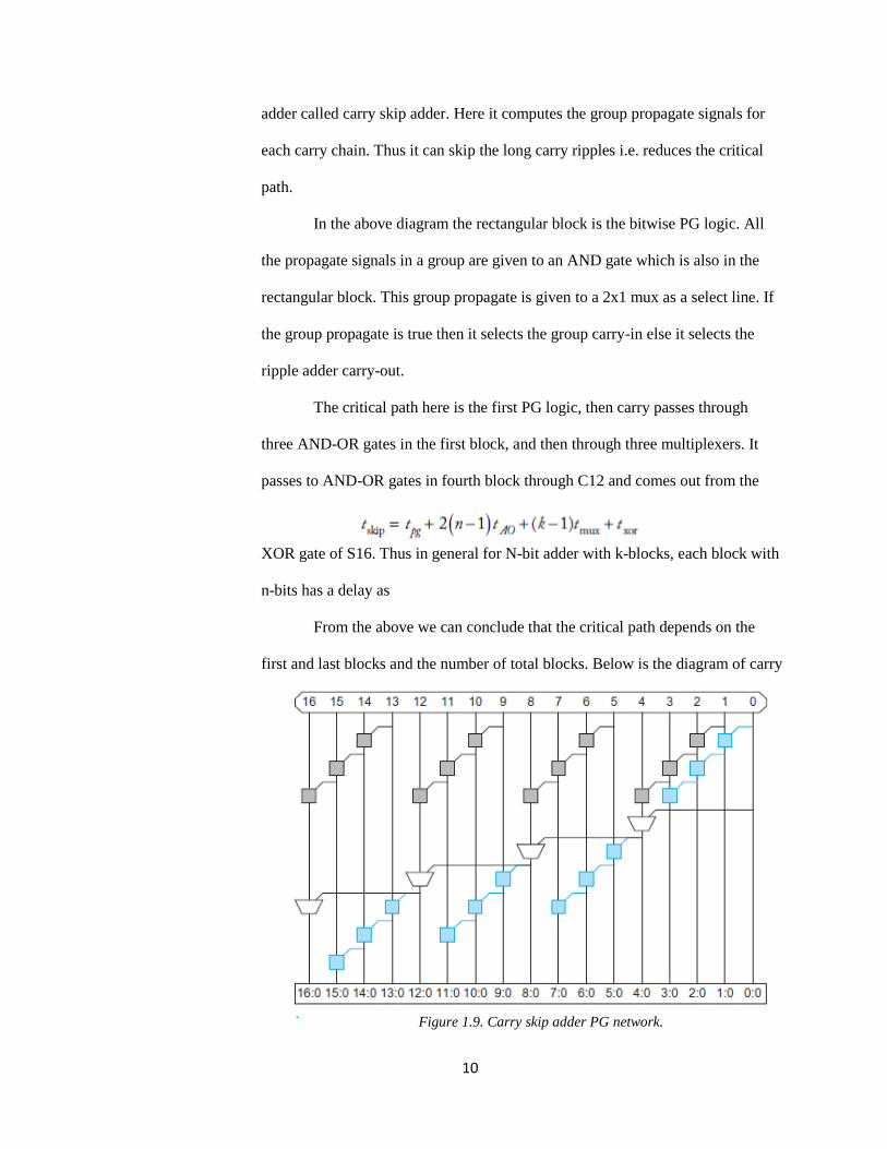
10
adder called carry skip adder. Here it computes the group propagate signals for
each carry chain. Thus it can skip the long carry ripples i.e. reduces the critical
path.
In the above diagram the rectangular block is the bitwise PG logic. All
the propagate signals in a group are given to an AND gate which is also in the
rectangular block. This group propagate is given to a 2x1 mux as a select line. If
the group propagate is true then it selects the group carry-in else it selects the
ripple adder carry-out.
The critical path here is the first PG logic, then carry passes through
three AND-OR gates in the first block, and then through three multiplexers. It
passes to AND-OR gates in fourth block through C12 and comes out from the
XOR gate of S16. Thus in general for N-bit adder with k-blocks, each block with
n-bits has a delay as
From the above we can conclude that the critical path depends on the
first and last blocks and the number of total blocks. Below is the diagram of carry
Figure 1.9. Carry skip adder PG network.

11
skip adder with 4 blocks and each block has 4-bits grouped together. I.e. they are
grouped as [4, 4, 4, 4].
The critical path can be reduced by reducing the number of bits in first
and last blocks and using larger blocks in the middle. Instead of grouping them as
[4,4,4,4] the critical path can be reduced by grouping the bits as [2,3,4,4,3]. This
is shown in the diagram below.
The cost of this carry skip adder is almost equal to the carry ripple adder.
For long adders if ripple carry adders are used then there will be more delay.
Instead carry skip adders can be used to reduce the delay and keeping the cost
low. However for long adders usually parallel prefix adders are used.
Figure 1.10. Carry skip adder with variable sizes of the blocks.

12
1.5. Carry look ahead adders (CLA): In carry skip adders multiplexers are used to
ripple the carry from previous block i.e. in critical path it has to wait for the carry
from the previous blocks. But in CLA each block generates a group propagate
and group generate signals as shown the figure.
The delay of this CLA with k blocks and each block has n-bits is
Where tpg(n) is the delay due to the AND-OR gates in the block used to compute
the group generate signal.
1.6. Carry select adder: In order to increase the speed of the response than the carry
look ahead adder or carry skip adder, this is designed. Here in each group it has 2
pairs of n-bit adders. One calculates the sum assuming the carry-in is zero and
Figure 1.11. Carry look-ahead adder
Figure 1.12. Carry select adder.

13
the other calculates assuming the carry-in is 1. Then a multiplexer is used where
the real carry-in is given to the select line. Thus depending upon the carry-in the
sum is selected. The delay caused due to this adder is given below.
In the carry select adder the n-bit adders which contain the PG logic and sum
XOR reduces the size by factoring out the common logic. If the multiplexer is
reduced to gray cell as shown in the figure then it becomes a carry increment
adder.
Figure 1.13. Carry increment adder PG network.
Here in carry increment adder there are black cells in each group which
determine the PG signals of the bits. The carry is generated from the gray cell
which is at the end of each column. The carry increment adder has more number

14
of cells than the regular ripple carry adder. As discussed in the carry select adders
the groups can be of variable length in order to reduce the delay of the critical
path.
Figure 1.14. Variable length carry increment adder.
Here the fan outs will be increased in between the groups. So, buffers are
to be used to drive these fan outs as shown below. Also buffers are used to
minimize the branching effort.
Figure 1.15. Carry increment adder with buffers.

15
In wide adders the carry select or the carry increment adders are used
multiple times. Like for a 64-bit adder four 16-bit carry select adders can be used.
Thus each block of 16-bit carry select adder propagates the carry to the next
block. From this a conditional sum adder can be derived. In this adder the carry
selection is performed on a single bit first and then for 2 bit, 4 bits recursively
doubling to N/2 bits. As shown in the figure below the top two rows has full
adders which compute sum and carry of bits considering the carry-in as 0 and 1
respectively.
Figure 1.16. 16-bit conditional sum adder.
The following rows have multiplexers which selects the sum and carry-
out for a carry-in of both 0 and 1 for each block of two. The next rows also
consists of multiplexers which give the sum and carry-out for a carry-in of

16
both 0 and 1 for each block of four and so on. Consider an example for
knowing how this conditional sum adder works.
Consider two N=16 bit variables a, b added using the conditional sum adder
with initial carry Cin = 0. In the first row the two pairs of full adders compute sum
and carry for carry-in 0 and 1. In the second row the adder selects the sum for the
upper half of the block based on the carry-out of the lower half (The block size =
2). This is done two times for both carry-in 0 and 1. In the next row the adder
again selects the sum for the upper half based on the carry-out of the lower half
(The block size here is 4). This process is repeated until the sum for 16-bit and
final carry are selected.

17
1.7. Tree adders or Parallel prefix adders: Usually for bigger adders the delay will
be more even if we use carry look ahead adders (or carry skip or carry select).
This delay can be reduced by looking ahead across the look ahead blocks i.e. a
tree of look ahead block structures.
These type of adders are often known as logarithmic adders, multilevel-
look ahead adders, and parallel prefix adders. This tree structure of look ahead
blocks can be constructed in different ways depending upon the application or on
various parameters like number of logic gates used, stages of logic, maximum
number of fan outs, amount of wiring etc.
There are mainly three types of parallel prefix adders
a) Brent kung adder
b) Kogge stone adder
c) Sklansky adder
a. Brent Kung adder: In the first row the prefixes are computed for 2-bit groups.
These in turn are used to find the prefixes for 4-bit groups, and then these are used to
compute prefixes for 8-bit groups and so forth. And these prefixes are fan back down
Figure 1.17. 16-bit Brent Kung adder.

18
to calculate the carry in of each bit. Brent Kung adder requires 2log2N stages. The
below figure of 16-bit Brent Kung adder shows that the fan-out is 2 at each stage and
where the buffers are used.
b. Kogge Stone adder: It is the widely used parallel prefix adder for 32-bit and 64-bit.
It has very less delay compared to the other adders. But the power consumption is
more and there are long wires to be connected between the cells. Also the number of
grey cells and black cells used are more compared to other tree structures.
c. Sklansky adder: In Sklansky intermediate prefixes are also computed along with the
long group prefixes. Because of which the fan outs will be increased. This results in
poor performance in case of wide adders. The performance can be increased with
Figure 1.18. 16-bit Kogge Stone adder.

19
Suitable buffering and transistor sizing. The delay can be reduced to log2N stages. It
is also similar to the conditional sum adder and also known as divide and conquer
tree adder. On the whole the critical path in these three tree structures is reduced to –
Figure 1.19. 16-bit Sklansky adder.

20
CHAPTER II
DESIGN AND IMPLEMENTATION
The layout of 32-bit Brent Kung adder is designed. At the beginning the layout of basic logic
gates like inverter, NAND, NOR, XOR are designed. Then the basic cells like gray cell, black
cell, PG logic, buffers are designed using the logic gates.
The inputs A and B are given to PG logic as shown in the block diagram. 32 PG
logic blocks are needed for a 32-bit adder. The outputs of this block are propagate (P)
and generate (G) signals. These signals are given to the tree structure of Brent Kung
adder. This structure contains grey cells and black cells arranged as discussed in
Figure 2.1. Block diagram of bit wise PG
logic. Figure2.2. Block diagram of Grey cell.

21
Brent Kung adder section. A grey cell has three inputs and one output as shown in the
figure. Generate and propagate signals from present stage and generate signal from
previous stage are inputs. Group generate signals is the output. Each stage ends with a
grey cell in any tree structure and the output of this grey cell is the group generate
signal which is considered as the carry of that stage.
Black cell has 4 inputs and 2 outputs. The inputs for a black cell are P and G
signals of present stage and P, G signals of previous stage.
Figure 2.3. Block diagram of Black cell

22
Below figures are the layouts of basic cells which are used to construct the 32-bit Brent
Kung adder.
Figure 2.4. Layout of Inverter

23
Figure 2.5. Layout of NAND Figure 2.6. Layout of NOR

24
Figure 2.7. Layout of AND logic gate.
Figure 2.8. Layout of OR logic gate.

25
Figure 2.9. Layout of XOR gate.
Figure 2.10. Layout of PG logic.
26
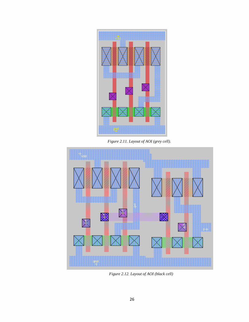
Figure 2.11. Layout of AOI (grey cell).
Figure 2.12. Layout of AOI (black cell)

27
A PG logic has an AND gate and XOR gate where AND gate is used to generate
G signal and XOR gate gives P signal. As discussed earlier to remove unnecessary
inverters two types of grey cells and black cells are used. These are inverting gates i.e. in
one row we use AOI (AND-OR-Inverter) for gray cell and black cell, in the next row we
use OAI (OR-AND-Inverter). So, layouts of two types of grey cell and black cell are
designed as shown in the above figures. The AOI cell takes the normal inputs and gives
inverted outputs and OAI takes inverted inputs and gives normal outputs.
The above figure is the 32-bit Brent Kung adder where AOI and OAI are used
alternatively for gray and black cells. The black and grey blocks represent black cells and
grey cells respectively. The circles represent buffers (inverters).
Figure 2.13. 32-bit Brent Kung adder block diagram

28
CHAPTER III
SOFTWARE USED
3.1. Magic: Magic is a software platform for designing VLSI circuit layouts. In Magic,
color graphics display can be used and a mouse or graphics tablet to design basic cells
and to combine them hierarchically into large structures. The most important difference
between magic and other layout design software is that it understands quite a bit about
the nature of circuits and uses this information to provide us with additional operations.
For example, Magic has built-in knowledge of layout rules; while editing, it continuously
checks for rule violations. Magic also knows about connectivity and transistors, and
contains a built-in hierarchical circuit extractor. Magic also has a plow operation that can
be used to stretch or compact cells. Lastly, Magic has routing tools that can be used to
make the global interconnections in circuits. Magic is based on the Mead-Conway style
of design. This means that it uses simplified design rules and circuit structures. The
simplifications make it easier for you to design circuits and permit Magic to provide
powerful assistance that would not be possible otherwise. However, they result in slightly
less dense circuits than you could get with more complex rules and structures. For
example, Magic permits only Manhattan designs (those whose edges are vertical or

29
horizontal). We think that the density sacrifice is compensated for by reduced design
time.
In Magic, a circuit layout is a hierarchical collection of cells. Each cell contains
three things: colored shapes, called paint, that define the circuit's structure; textual labels
attached to the paint; and sub cells, which are instances of other cells.
The two basic layout operations are painting and erasing. They can be invoked
using the :paint and :erase
commands, or using the mouse buttons.
:paint layers (paints rectangular regions, specified by the box)
:erase layers (deletes the specified layers from the region under the box)
In each of these commands layers is one or more names separated by commas. In Magic
there is one paint layer for each kind of conducting material (polysilicon, ndiffusion, metal1,
etc.), plus one additional paint layer for each kind of transistor (n-transistor, p-transistor, etc.),
and, finally, one further paint layer for each kind of contact (pcontact, ndcontact, m2contact, etc.).
Figure 3.1. Colors of metals and layers used in magic layout tool

30
The easiest way to paint and erase is with mouse buttons. To paint, position the box over
the area you'd like to paint, then move the cursor over an existing color and click the middle
mouse button (i.e. click both the left and the right mouse button at the same time on a two-button
mouse). To erase everything in an area, place the box over the area, move the cursor over a blank
spot, and click the middle mouse button. While you are painting, white dots may occasionally
appear and disappear. These are design rule violations and will be explained in Design Rule
Checking.
To make the layout readable or for layout extraction and simulation labeling is necessary.
The inputs, outputs and required nodes should be labeled. Labeling can be done by the following
command.
:label labelname
Another feature of magic is its design rule checking (DRC). There are certain predefined
rules while designing the layout that should be satisfied so that the IC is fabricated without errors.
In general, design rules specify how far apart various layers must be, or how large various aspects
of the layout must be for successful fabrication, given the tolerances and other limitations of the
fabrication process. If there is any mistake made magic will show them in the form of white dots.

31
We can even know the reason why the error occurred by using the following command and can
make changes in our layout.
:drc why or macro y.
In the above figure the notations of the layers are given which are used in the commands while
designing the layout.
3.2. IRSIM: IRSIM, is a fast switch-level simulator designed to work with an extracted Magic
layout. Simulating an extracted layout allows you to check the functionality of a MOS layout at a
detailed level as well as providing first-order performance measurements.
IRSIM files are text files with the extension .sim that contain the description of an entire circuit.
IRSIM files can be created by hand or extracted from Magic. To functionally verify the magic
layout the IRSIM file must be extracted from the .mag file. Power nodes must be labeled as
“Vdd” and “Gnd” for IRSIM to recognize them correctly. Each node can be referred in IRSIM by
their Magic label name. The first step is to extract the simulation data from your Magic layout is
extracting the magic layout or creating an .ext file
magic> extract all
Figure 3.2. Commands used for the layers

32
#The basic idea of IRSIM is you tell it which nodes to pull high, low, and tri state. Then you tell
IRSIM to run the simulation for a certain period of time. This period of time is the step size. The
'step size' command tells IRSIM what the step size should be, the default is 10ns.
irsim> stepsize 50
# The 'w' command tells IRSIM to watch the nodes change. The command below tells it to watch
the nodes A, B and Z. IRSIM displays the nodes in the opposite order of that set by the command,
therefore the output order will be A B Z. This is just a matter of personal preference though. Enter
the nodes in any order you like.
irsim> w Z B A
# 'd' displays all the nodes that are being watched. You can also enter in something like’d A'
which tells IRSIM to only display the node A.
irsim> d
| A=X B=X Z=X
| time = 0.00ns
# At time zero, the values for the nodes are all undefined. The 'l' command forces the nodes to a
logic value of 0.
irsim> l A B
# 's' simulates for the period of time previously defined by the 'step size' command. IRSIM
displays the value of each node being watched after each step.
irsim> s
| A=0 B=0 Z=1

33
| time = 50.00ns
#the 'h' command sets the following nodes to a logic value of 1.
irsim> h A B
irsim> s
| A=1 B=1 Z=0
| time = 100.00ns
# the 'path' command shows the critical path for the last node transition. The output shows that an
input node A changed to logic 1 at time = 50.00 ns. Then node Z changed to 0 at time = 50.01 ns.
Therefore it took 0.01 ns to go from high to low for the given input change.
irsim> path Z
| critical path for last transition of Z:
| A -> 1 @ 50.00ns , node was an input
| Z -> 0 @ 50.01ns (0.01ns)
# if there is a long list of nodes, it can be tiresome to keep using the l and h commands to set their
logic values. The 'vector' command lets you group nodes together so you can set them all quickly.
The command below tells IRSIM to group the nodes A and B into a vector In. The first node will
be the MSB.
irsim> vector In B A
#the 'setvector' command tells IRSIM to set the value of a vector. The first command below sets
the vector In to 00, therefore A=0 and B=0. The following commands demonstrate how you can
create a truth table using the vector In
irsim> setvector In 00
34
irsim> s
| A=0 B=0 Z=1
| time = 150.00ns
irsim> setvector In 01
irsim> s
| A=1 B=0 Z=1
| time = 200.00ns
irsim> setvector In 10
irsim> s
| A=0 B=1 Z=1
| time = 250.00ns
irsim> setvector In 11
irsim> s
| A=1 B=1 Z=0
| time = 300.00ns
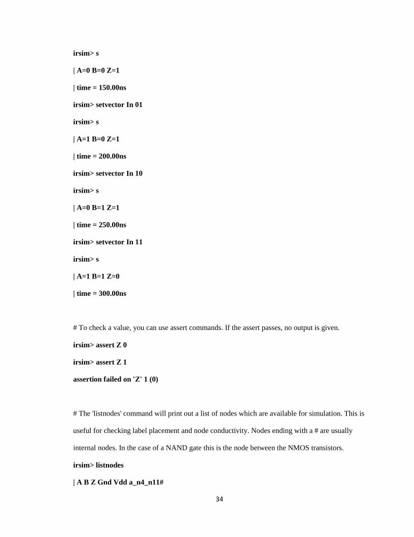
# To check a value, you can use assert commands. If the assert passes, no output is given.
irsim> assert Z 0
irsim> assert Z 1
assertion failed on 'Z' 1 (0)
# The 'listnodes' command will print out a list of nodes which are available for simulation. This is
useful for checking label placement and node conductivity. Nodes ending with a # are usually
internal nodes. In the case of a NAND gate this is the node between the NMOS transistors.
irsim> listnodes
| A B Z Gnd Vdd a_n4_n11#

35
The analyzer window is a useful graphical logic analyzer used to debug the operation of a design.
Signals can take on the values {0, 1, X}. Once the simulation is started the value of any signal
change can be seen in the analyzer window. You can view the analyzer window using the
command ‘analyzer’ or 'ana'. The analyzer can also be started by following the command with
the names of available nodes. If the window is already visible this will append the nodes to the
list.
irsim> analyzer A B Z
or
irsim> ana A B Z
36
CHAPTER IV
RESULT ANALYSIS
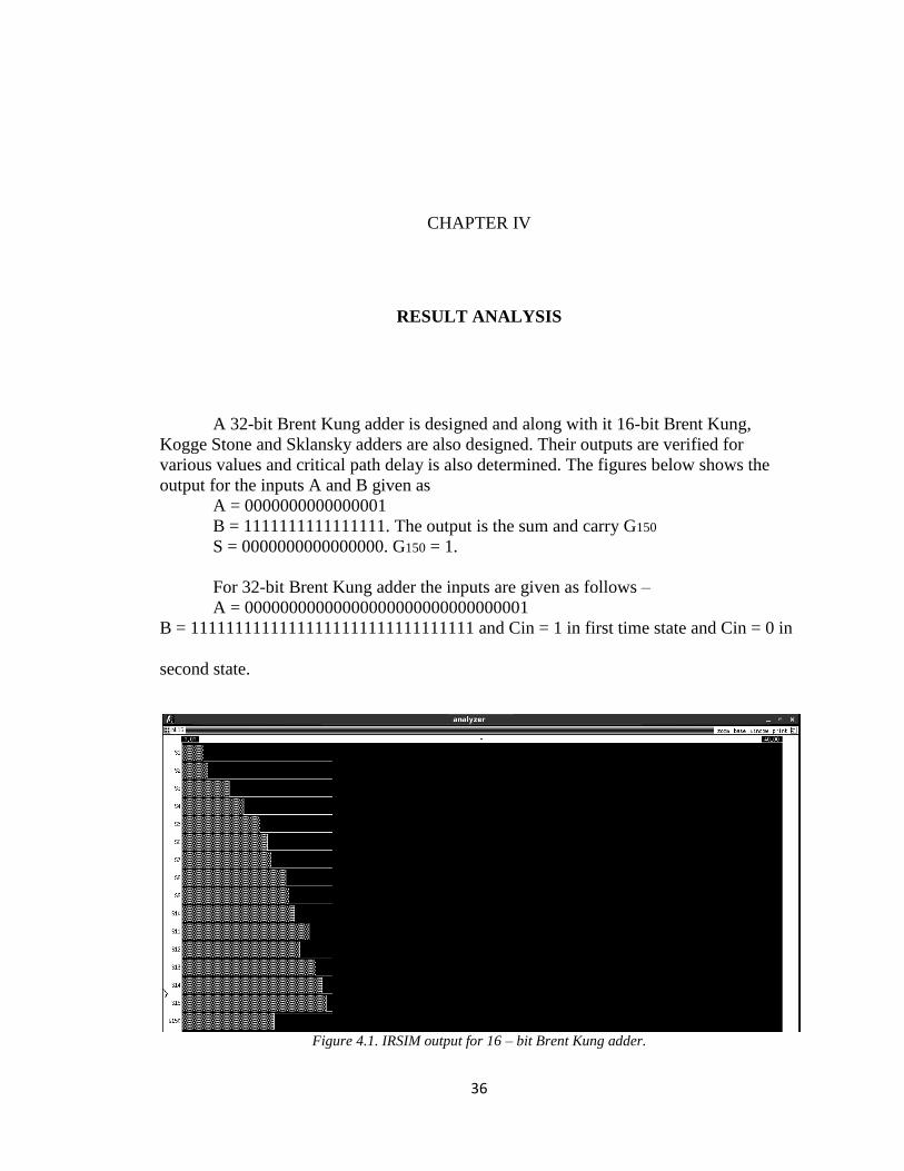
A 32-bit Brent Kung adder is designed and along with it 16-bit Brent Kung,
Kogge Stone and Sklansky adders are also designed. Their outputs are verified for
various values and critical path delay is also determined. The figures below shows the
output for the inputs A and B given as
A = 0000000000000001
B = 1111111111111111. The output is the sum and carry G150
S = 0000000000000000. G150 = 1.
For 32-bit Brent Kung adder the inputs are given as follows –
A = 00000000000000000000000000000001
B = 11111111111111111111111111111111 and Cin = 1 in first time state and Cin = 0 in
second state.
Figure 4.1. IRSIM output for 16 – bit Brent Kung adder.

37
Figure 4.2. The critical path delay for 16-bit Brent Kung adder.
Figure 4.3. IRSIM output of 16-bit Kogge Stone adder.

38
Figure 4.4. The critical path delay for 16-bit Kogge Stone adder
Figure 4.5. IRSIM output for 16-bit sklansky adder

39
Figure 4.6. Critical path delay for 16-bit Sklansky adder
Figure 4.7. IRSIM output for 32-bit Brent Kung adder.

40
Figure 4.8. The critical path delay for 32-bit Brent Kung adder.

41
CHAPTER V
CONCLUSION AND FUTURE WORK
Initially the layouts of 16-bit Brent Kung, Sklansky, Kogge Stone adders are designed. The delay
or the critical path is computed for these adders using the simulator IRSIM. Then 32-bit Brent
Kung adder layout is designed with minimum width (width = 5λͅ) and its delay is calculated. The
below graph shows the delays of the 16-bit adders and 32-bit Brent Kung adder respectively.
Apart from the critical path the delays for various sets of inputs are observed and compared
among all the layouts.
From the outputs we got, it can be concluded that Kogge Stone adder has minimum delay
compared to the other two adders but the amount of wiring is more in it. The Sklansky adder has
more delay than the other two and also has more fan-outs. Brent Kung adder is the simple
structure with minimum fan-outs and wiring.
These layouts are designed using CMOS logic and can be compared with other technologies like
CPL (complementary pass transistor logic). The widths of the transistors can be changed as per
the RC delay model proposed by Sunil Kumar Lakkakula (PhD Student under Dr. L.G. Johnson)
so that the delay can be reduced to much lower value.

42
Figure 5.1. Graph indicating the delays of the adders designed.

43
CHAPTER VI
REFERENCES
1. P. Chaitanya kumara, R. Nagendra “Design of 32 bit parallel prefix adders” IOSR journal
of electronics and communication engineering (IOSR-JECE) - (may. - jun. 2013), pp 01-06
2. R. P. Brent and H. T. Kung, “A Regular Layout For Parallel Adders”, IEEE trans,
computers, vol.c-31, pp. 260-264, .March 1982.
3. CMOS VLSI design: A circuits and systems perspective (4th edition) [Neil Weste, David
Harris]
4. Vikramkumar Pudi and K. Sridharan, “Low complexity design of ripple carry and Brent–
Kung adders in QCA” IEEE transactions on nanotechnology, vol. 11, no. 1, January 2012.
5. Anas Zainal Abidin et al: “4-bit Brent Kung parallel prefix adder simulation study using
silvaco EDA tools”
6. Ireneusz Brzozowski, Damian Pałys, Andrzej kos1 “An analysis of full adder cells for
low-power data oriented adders design” 20th international conference "Mixed design of
integrated circuits and systems", June 20-22, 2013, Gdynia, Poland.
7. Padma Devi, Ashima Girdher, Balwinder Singh “Improved carry select adder with
reduced area and low power consumption” International journal of computer applications (0975
– 8887) volume 3 – no.4, June 2010
8. Adilakshmi Siliveru, M.Bharathi “Design of Kogge-Stone and Brent-kung adders using
degenerate pass transistor logic” International journal of emerging science and engineering
(IJESE)ISSN: 2319–6378, volume-1, issue-4, February 2013
9. http://www.ece.iit.edu/~eoruklu/courses/ece429/tutorial/magic.html

44
10. http://fp.okstate.edu/lgjohn/cadtools/magic/index.html
11. http://www.ece.ucdavis.edu/~bbaas/116/docs/irsim_tut_2010.01.27.doc

VITA
Vinish Kalva
Candidate for the Degree of
Master of Science
Thesis: LAYOUT DESIGN OF 32-BIT BRENT KUNG ADDER (CMOS LOGIC)
Major Field: Electrical and Computer Engineering.
Biographical:
Education:
Completed the requirements for the Master of Science in Electrical and
Computer Engineering at Oklahoma State University, Stillwater, Oklahoma in
May, 2015.
Completed the requirements for the Bachelor of Technology in Electronics and
Communication Engineering at Acharya Nagarjuna University, Vijayawada,
A.P, India in 2013.