
Valuation of Assets and “Other Liabilities” - EIOPA Registers
Upload
khangminh22Category
view
1download
0
2
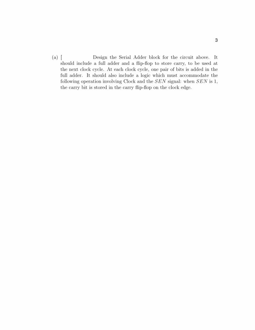
Consider the serial adder below. Two shift registers SREG1 andSREG2 are used to hold the four bit numbers to be added. Each register hasa Shift Enable signal SEN, serial input SI, Clock and Reset. When SEN = 1and the Clock is pulsed, SI is entered into the Most significant bit, MSB, ofthe register, as the contents of the register are shifted right one position. Theconnections needed for initial loading of the registers are not shown. The upperregister serves as accumulator, and after four shifts its contents is replaced withthe sum of the initial numbers. The lower register is connected as a cyclicshift registers, so after four shifts it is back to its original state and the secondnumber is not lost.
SREG1 SI SEN LSB RST CLK
SREG2 SI SEN LSB RST CLK
Serial Adder Sum
CarryOut
Controller
Clock
Reset
TOPIC: Digital System Design (ENEL453)
Q.1 (parts a-c on following pages)
3
(a) [ Design the Serial Adder block for the circuit above. Itshould include a full adder and a flip-flop to store carry, to be used atthe next clock cycle. At each clock cycle, one pair of bits is added in thefull adder. It should also include a logic which must accommodate thefollowing operation involving Clock and the SEN signal: when SEN is 1,the carry bit is stored in the carry flip-flop on the clock edge.

4
(b) Design the Controller (based on a Mealy FSM) so that afterreceiving a start signal, N , it will output SEN = 1 for four clocks andthen stop. SEN = 1 shifts the sum bit into the upper register and causesthe lower register to rotate right. Draw the state graph and the statetable. Assume that the start signal N is terminated before the networkreturns to the first state, so no further action occurs until another startsignal is received. Once the second state is reached, the network operationcontinues regardless of the value of N .
(c) Provide an alternative high-level FSM for the FSM in part(b).

5
Consider the VHDL code that defines a debounce circuit, whichcan be used to qualify the input of a push-button switch.
library ieee;
use ieee.std logic 1164.all;
use ieee.std logic arith.all;
entity DEBOUNCE is
port(INP, RST, CLK: in std logic;
OUTP: out std logic;
end entity DEBOUNCE;
architecture BEHAV of DEBOUNCE is
signal D1, D2, D3: std logic;
begin
process (CLK, RST)
begin
if (RST = ’1’) then
D1 <= ’0’;
D2 <= ’0’;
D3 <= ’0’;
elsif (CLK’event and CLK = ’1’) then
D1 <= INP;
D2 <= D1;
D3 <= D2;);
end if;
end process;
OUTP <= D1 and D2 and (not D3);
end architecture BEHAV;
(a) Draw the circuit and its timing diagram (see the templatebelow) to answer the question: why this circuit is called a debounce circuit?
Q.2 (parts a-d on this and following pages)

6
CLK
RST
INP
D1
D2
D3
OUTP
(b) In addition, the circuit ensures that the output indicating thebutton press is of fixed duration regardless of how long the actual buttonis pressed. How long is this fixed duration?

7
(c) Propose an alternative debounce circuit solution, based on acounter (draw the design schematics). Specify the counter size.
(d) Provide the VHDL fragment corresponding to the debouncerbased on the counter from part (c) in the space provided below.
library ieee;
use ieee.std logic 1164.all;
use ieee.std logic arith.all;
entity DEBOUNCE1 is
port
end entity DEBOUNCE1;
architecture BEHAV of DEBOUNCE1 is
end architecture BEHAV;

TOPIC: Digital Ciruits (ENCM467)
Q.1

Q.2
Q.3

TOPIC: Embedded system interfacing (ENCM511)
1) A developer has a microprocessor that transmits to 4 external peripherals over 3 SPI lines, a common industrial situation.
(i) Draw a labelled diagram of this configuration.
(ii) Using this diagram, explain the basics of the SPI interface, and detail how it is possible for a microprocessor to control 4
peripherals over 3 SPI lines
(iii) Actual there are 5 spi-lines needed if you take into account the transmission of information from the peripherals to the
processor – MISO and GND (ground). Explain why the performance of the SPI interface will / may be unreliable if there is a
missing ground wire
2) Using brief examples, explain the relationship between and / or differences off these terms associated with editing a
program: compiling, linking and downloading the code to a microprocessor evaluation board.
Source file, Object files, Executable, library file, linker error, JTAG- interface, boot-code
3) Discuss and calculate the execution time difference of C++ algorithm running on a 300 MHz processor designed with and
without a 4 instruction pipeline (Fetch, decode, execute, writeback). Assume that the machine code generated from the
C++ algorithm requires 1 jump / call / return instruction for every 20 lines of code.
4) Discuss and calculate the execution time difference of C++ algorithm running on a 300 MHz processor designed with and
without a 4 instruction pipeline (Fetch, decode, execute, writeback) when an external device is generating a 1 MHz
interrupt signal which are serviced by a short ISR routine (100 instructions). Assume that the machine code generated from
the C++ algorithm requires 1 jump / call / return instruction for every 20 lines of code.
TOPIC: Advanced processor architectures (ENCM515)
1) Draw labelled diagrams that illustrate the basic characteristics of Harvard and von-Neumann processors. Explain how these
architectural differences impacts the execution times of the following 2 functions.
2) Explain and contrast the execution speed advantages of the following concepts found on many modern processor:
a. SISD, SIMD, super-scalar instructions
b. Large data blocks (256 WORDS OR MORE) being send to peripherals controlled with, or without, the use of DMA
activity
3) A key advantage of many modern microprocessors is their ability to handle real-time audio operation, e.g. digital filtering.
a. Explain what is meant by “real-time” or “non-real” time audio operations
b. Draw the block diagram of a microprocessor system with A/D and D/A capable of sampling at 8 kHz, which has
been coded with a low-pass digital filter with 400 Hz bandwidth.
c. For your system, what will be the output from the processor if it is receiving an audio signal with components at
65Hz, 2065Hz and 4065Hz? Explain your answer.
float DoSum(int number) { float sum = 0.0; for (int count = 0; count < number) {
sum = 2 * count; } return sum; }
float DoSumWithMemory(int number, float *pt ){ float sum = 0.0; for (int count = 0; count < number) {
sum = 2 * count + *pt++; } return sum; }

TOPIC: Computer Arithmetic & Computational Complexity (ENCM517)
Q1. Convert integers (say, 1009) from binary to Booth encoding and explain why it is beneficial for implementing a constant multiplication operation
Q2. Show the work of RSA encryption algorithm for a specified key parameters.
Q3. Compute the connectivity matrix of a given graph
Q4. Show the relationship between given algorithmic problems (say, solving system of linear equations for a) symmetric and b) non-symmetric matrices).

Field of Study Examination, Feb 24 2017
Subject area: Computer Engineering
This question paper has 4 pages (not including this cover page).
This question paper has 4 questions.
Answer a minimum of one question and at most three questions from this subjectarea.
Use a separate booklet (i.e., blue booklet) for the answers to questions in thissubject area.

1. This question has two parts (a)-(b).
(a) Draw labelled diagrams that illustrate the basic bus characteristics of Harvard and von-
Neumann processors. Show where data arrays, C++ code and ASM code will be stored.
(b) Explain how these architectural differences impacts the execution time of the following FIR
filter and calculate the ratio of execution speeds.
volatile float FIFO[256] = {0.0};
volatile float coeffs[256] = {.....}
// Assume correctly populated with FIR filter values to perform
// 200 Hz low pass filter at 40 kHz sampling rate
float FIR(float newValue, int numFIRtaps){
if (numFIRtaps > 256) exit(1);
// Adjust FIFO buffer
for (int count = 1; count < numFIRtaps; count++){
FIFO[count - 1] = FIFO[count];
}
FIFO(numFIRtaps - 1) = newValue; // Insert new value
sum = 0.0;
for (int count = 0; count < numFIRtaps; count++){
sum = sum + FIFO[numFIRtaps - 1 - count] * coeffs[count];
}
return sum;
}
1/4

2. This question has 3 parts (a)-(c). Note that this question also appears in the Circuits
and Electronics exam. If you attempt this question, it will only count once, towards
whichever exam you attempt it in.
(a) Consider the circuit below.
Consider implementing the circuit on an FPGA. Create a sketch of such implementation using
the two CLBs shown below.
LUT D Q
CLK
LUT D Q
CLK
CLB
LUT D Q
CLK
LUT D Q
CLK
CLB
(b) Show the content (the function truth tables) of the used LUTs.
(c) Create an FSM based on the circuit in (a). Assume that reset resets to the first state. Derive
the excitation and output equations.
2/4

3. This question has 3 parts (a)-(c).
(a) Explain how the circuit shown below works when the CLK is on and off. What type of circuit
is this?
(b) Explain how the astable circuit shown below works. If the propagation delay of each inverter
is 1 ns, what is the frequency of the oscillation of the circuit?
(c) Design a 4 bit pre-charged NAND ROM that will store the words below. Mark your Bit Line
(BL) and your word lines and indicate for what value the Word Line (WL) will be enabled.WL [0]
WL [1]
WL [2]
WL [3]
=
1 0 0 1
0 1 1 0
0 0 1 0
1 1 1 1
3/4

4. This question has 3 parts (a)-(c).
(a) Describe what is an NP-hard problem. And give an example of an NP-hard problem.
(b) For the circuit given below draw the hyper-graph and graph representations and its connectivity
matrix. Assume that the weights of all wires in the graph representation are equal to one.
A
B
C
n1
n2
n7D
n3
F
E
n4
n5
G
n6H
(c) The following algorithm is given. Each operation in the algorithm except for the multiplication
takes 1 unit of time and multiplication takes 10 units of time. Calculate the total time for the
execution of the algorithm as a function of N .
Algorithm Find the product of integers from 1 to N
1. fact ← 1;
2. x ← 2;
3. while x ≤ N do
4. fact ← fact × x ;
5. x ← x+ 1;
6. end while
4/4
Copyright © 2022 FDOKUMEN