Sleepy Keeper Approach for Common Source CMOS Amplifier for Low-Leakage Power VLSI Design.
7
[Hafeez et al., 3(4): April, 2014] ISSN: 2277-9655 Impact Factor: 1.852 http: // www.ijesrt.com(C)International Journal of Engineering Sciences & Research Technology [4096-5002] IJESRT INTERNATIONAL JOURNAL OF ENGINEERING SCIENCES & RESEARCH TECHNOLOGY Sleepy Keeper Approach for Common Source CMOS Amplifier for Low-Leakage Power VLSI Design Mohamed Azeem Hafeez *1 , Anuj Shaw 2 *1 Assistant professor, Department of ECE, SirMVIT Bangalore, India 2 Research scholar New Delhi, India [email protected] Abstract As the scaling goes deep into nano-meter range the leakage power dissipation has overtaken the dynamic power dissipation in VLSI circuits. The demand for low power consumer electronic gadgets which are portable reliable and with a long battery life has necessitated the circuits which have low power dissipation in their standby and active mode of operation. Sleepy keeper is one such technique which aims to reduce the leakage power. This paper attempts to implement the sleepy keeper (SK) approach for the common source (CS) amplifier since amplifiers are one of the important circuits in analogue and digital integrated circuit design. The leakage and dynamic power dissipation, Area and the logical states are analysed over different technologies. It is observers that there is reduction in leakage power dissipation of sleepy keeper common source amplifier (SKCSA) as compared to normal CS CMOS amplifier in different technology Keywords: Sleepy Keeper, Leakage Power, Zigzag, Stack, Common source amplifier. Introduction The demand for portable electronic gadgets which are small reliable and with a long battery life has led to rampant scaling which has led to the reduction in feature size of the device and the ill effect of this process has led to an increase in leakage power dissipation even when the device is non operational. Various techniques have been evolved over the years to counter the increase in leakage power. Each technique has its own advantage and disadvantage for its application. A new approach called as sleepy keeper was proposed for low leakage which has been applied in the design of common source amplifier circuits in this paper. A comparative study is carried out with the base common source amplifier circuit and its sleepy keeper counterpart. Previous Work Sleep approach: We will review some of the subthreshold leakage technique at circuit level. The known solution is the sleep approach method. In the sleep approach, both an additional "sleep" PMOS transistor is placed between VDD and the pull-up network of a circuit and an additional "sleep" NMOS transistor is placed between the pull-down network and GND. The sleep transistors are turned on when the circuit is operational and turned off when the circuit is in idle state. These sleep transistors turn off the circuit by cutting off the power rails. By isolating the power source, this technique can reduce leakage power effectively. However, output will be undetermined after sleep mode, so the technique results in loss of idle state and a floating output voltage. Figure 1 shows its structure. Fig.1 Sleep approach
Transcript of Sleepy Keeper Approach for Common Source CMOS Amplifier for Low-Leakage Power VLSI Design.

[Hafeez et al., 3(4): April, 2014] ISSN: 2277-9655
Impact Factor: 1.852
http: // www.ijesrt.com(C)International Journal of Engineering Sciences & Research Technology
[4096-5002]
IJESRT INTERNATIONAL JOURNAL OF ENGINEERING SCIENCES & RESEARCH
TECHNOLOGY
Sleepy Keeper Approach for Common Source CMOS Amplifier for Low-Leakage
Power VLSI Design Mohamed Azeem Hafeez*1, Anuj Shaw2
*1 Assistant professor, Department of ECE, SirMVIT Bangalore, India 2 Research scholar New Delhi, India
Abstract As the scaling goes deep into nano-meter range the leakage power dissipation has overtaken the dynamic
power dissipation in VLSI circuits. The demand for low power consumer electronic gadgets which are portable reliable
and with a long battery life has necessitated the circuits which have low power dissipation in their standby and active
mode of operation. Sleepy keeper is one such technique which aims to reduce the leakage power. This paper attempts
to implement the sleepy keeper (SK) approach for the common source (CS) amplifier since amplifiers are one of the
important circuits in analogue and digital integrated circuit design. The leakage and dynamic power dissipation, Area
and the logical states are analysed over different technologies. It is observers that there is reduction in leakage power
dissipation of sleepy keeper common source amplifier (SKCSA) as compared to normal CS CMOS amplifier in
different technology
Keywords: Sleepy Keeper, Leakage Power, Zigzag, Stack, Common source amplifier.
Introduction The demand for portable electronic gadgets
which are small reliable and with a long battery life
has led to rampant scaling which has led to the
reduction in feature size of the device and the ill effect
of this process has led to an increase in leakage power
dissipation even when the device is non operational.
Various techniques have been evolved over the years
to counter the increase in leakage power. Each
technique has its own advantage and disadvantage for
its application. A new approach called as sleepy
keeper was proposed for low leakage which has been
applied in the design of common source amplifier
circuits in this paper. A comparative study is carried
out with the base common source amplifier circuit and
its sleepy keeper counterpart.
Previous Work Sleep approach:
We will review some of the subthreshold
leakage technique at circuit level. The known solution
is the sleep approach method. In the sleep approach,
both an additional "sleep" PMOS transistor is placed
between VDD and the pull-up network of a circuit and
an additional "sleep" NMOS transistor is placed
between the pull-down network and GND.
The sleep transistors are turned on when the circuit is
operational and turned off when the circuit is in idle
state. These sleep transistors turn off the circuit by
cutting off the power rails. By isolating the power
source, this technique can reduce leakage power
effectively. However, output will be undetermined
after sleep mode, so the technique results in loss of idle
state and a floating output voltage. Figure 1 shows its
structure.
Fig.1 Sleep approach

[Hafeez et al., 3(4): April, 2014] ISSN: 2277-9655
Impact Factor: 1.852
http: // www.ijesrt.com(C)International Journal of Engineering Sciences & Research Technology
[4096-5002]
Zigzag Approach
A modification of the sleep approach, results
in the zigzag technique, which helps to reduce
overhead caused by sleep transistors by placing the
transistors in alternate fashion with a particular pre-
selected input vector. The structure is shown in Figure
2. we assume that, in sleep mode, the input of the logic
is ‘0’ and each logic stage reverses its input signal, i.e.,
the output is ‘1’ if the input is ‘0,’ and the output is ‘0’
is the input is ‘1.’ If the output is ‘1,’ then a sleep
transistor is added to the pulldown network; if the
output is ‘0’, then a sleep transistor is added to the pull-
up network. Thus, the zigzag approach uses fewer
sleep transistors than the original sleep approach.
Furthermore, this approach still results in destruction
of state (i.e., state is set to the particular pre-selected
input vector), although the problem of floating output
voltage is eliminated.
Fig.2 Zigzag approach
Stack Approach
The stack approach creates a stack effect the
size of one transistor into two half sized transistors.
When the two transistors are turned off it causes a
reverse bias across them there by reducing the
subthreshold leakage conduction. But the
disadvantage is that it leads to increase in propagation
delay. The structure of stack approach is shown in
figure 3.
Fig 3 Stack approach
Sleepy Stack Approach
Combination of sleep and stack approach
gives us sleepy stack approach. This technique divides
existing transistors into two half size transistors like
the stack approach. Then sleep transistors are added in
parallel to one of the divided transistors. Figure 4
shows its structure. During sleep mode, sleep
transistors are turned off and stacked transistors
oppose leakage current while maintaining the state.
Each sleep transistor, placed in parallel to the one of
the stacked transistors, reduces resistance of the path;
as a result delay is decreased during active mode.
There is increase in area for this techniques since each
transistor is replaced by three transistors and
additional wires are added for pull-up (S) and pull-
down (S’), which are sleep signals.
Fig.4 Sleepy stack approach
For the sleep, zigzag, sleepy stack dual Vth
technology can be applied to obtain leakage power
reduction. Since high-Vth results in less leakage but
lowers performance, high-Vth is applied only to
leakage reduction transistors, which are sleep

[Hafeez et al., 3(4): April, 2014] ISSN: 2277-9655
Impact Factor: 1.852
http: // www.ijesrt.com(C)International Journal of Engineering Sciences & Research Technology
[4096-5002]
transistors, and any transistors in parallel to the sleep
transistors; on the other hand, low-Vth is applied to the
remaining transistors to maintain logic performance
Sleepy Keeper Approach The structure and operation of sleepy keeper
is discussed in this section. In addition, we discuss
some layout issues for the sleepy keeper approach
Fig 5 Sleepy keeper approach
The typical CMOS technique uses PMOS
and NMOS transistor to connect to power supply VDD
and ground respectively. Since NMOS transistor pass
weak logical ‘1’, to maintain a value of ‘1’ in sleep
mode, given that the ‘1’ value has already been
calculated, the sleepy keeper approach uses this output
value of ‘1’ and an NMOS transistor connected to
VDD to maintain output value equal to ‘1’ when in
sleep mode. As shown in Figure 5, an additional single
NMOS transistor placed in parallel to the pull-up sleep
transistor connects VDD to the pull-up network. When
in sleep mode, this NMOS transistor is the only source
of VDD to the pull-up network since the sleep
transistor is off.
We know that PMOS transistor pass weak
logical ‘0’, to maintain a value of ‘0’ in sleep mode,
given that the ‘0’ value has already been calculated,
the sleepy keeper approach uses this output value of
‘0’ and a PMOS transistor connected to GND to
maintain output value equal to ‘0’ when in sleep mode.
As shown in Figure 6 which is the inverter in sleepy
keeper approach, an additional single PMOS transistor
placed in parallel to the pull-down sleep transistor is
the only source of GND to the pull-down network
which is the dual case of the output ‘1’ case explained
above.
In order to maintain a proper logical state we
need the NMOS connected to VDD and the PMOS
connected to GND. The researchers have show that we
can use relatively less VDD in order to maintain the
proper logical states during and sleep mode of
operation.
Common Source Amplifier
Fig 6 CS amplifier
Common source (CS) amplifier is one of the
basic configurations in MOSFET. It is commonly used
as voltage or transconductance amplifier. The input
voltage modulates the amount of current flowing
through the load and hence the voltage across it. It is
called as common source because the source terminal
is common for input and output signal. The structure
of CS amplifier is shown in figure 6.
Fig 7 SKCSA
For the sleepy keeper approach, a PMOS
must be connected to GND and an NMOS must be
connected to VDD as explained in the previous
section. The schematic for CS amplifier with sleepy
keeper is shown in figure 7
Experimental Results The schematics were simulated using the
DSCH and Microwind software. The CS amplifier, CS
amplifier with sleepy keeper, basic inverter and the

[Hafeez et al., 3(4): April, 2014] ISSN: 2277-9655
Impact Factor: 1.852
http: // www.ijesrt.com(C)International Journal of Engineering Sciences & Research Technology
[4096-5002]
sleepy keeper version of the inverter were simulated
for 90nm, 65nm and 45nm technologies. The
simulated waveforms are shown in the figure (8-9)
below .The dynamic, static power dissipation and area
of the above circuits for various technologies is
tabulated in figure (20-23)
The supply voltages used by the technologies are
tabulated in Table 1.
Tech. 90nm 65nm 45nm
Vdd 1.2v 0.7v 0.35v
Table 1 Supply voltages for different technologies.
Fig 8 Waveform of CS amplifier in 90nm
Fig 9 Waveform of CS amplifier in 65nm
Fig 10 Waveform of CS amplifier in 45nm
Fig 11 Waveform of SKCSA in 90nm
Fig 12 Waveform of SKCSA in 65nm
[Hafeez et al., 3(4): April, 2014] ISSN: 2277-9655
Impact Factor: 1.852
http: // www.ijesrt.com(C)International Journal of Engineering Sciences & Research Technology
[4096-5002]
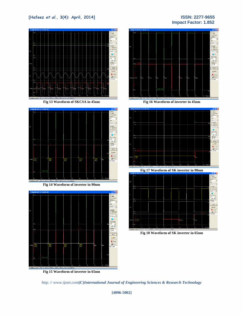
Fig 13 Waveform of SKCSA in 45nm
Fig 14 Waveform of inverter in 90nm
Fig 15 Waveform of inverter in 65nm
Fig 16 Waveform of inverter in 45nm
Fig 17 Waveform of SK inverter in 90nm
Fig 18 Waveform of SK inverter in 65nm

[Hafeez et al., 3(4): April, 2014] ISSN: 2277-9655
Impact Factor: 1.852
http: // www.ijesrt.com(C)International Journal of Engineering Sciences & Research Technology
[4096-5002]
Fig 19 Waveform of SK inverter in 45nm
Fig 20 comparison chart for CS amplifier
Fig 21 comparison chart for SKCSA
Fig 22 comparison chart for inverter
Fig 23 comparison chart for SK inverter
Conclusion Scaling down of the CMOS technology
feature size and threshold voltage for achieving high
performance has resulted in increase of leakage power
dissipation. We have presented an efficient
methodology for reducing leakage power in VLSI
design. The sleepy keeper technique results in ultra
low static power consumption with state saving.
Furthermore, the sleepy keeper approach is applicable
to single and multiple threshold voltages. With
application of dual Vth, sleepy keeper is the most
efficient approach to reduce leakage current with the
smallest delay and area increases while
simultaneously preserving precise logic state in sleep
mode. In terms of area, the sleepy keeper approach is
expected to be more attractive for complex logic
circuits, because the portion of increased area for the
required additional transistors will be smaller for
complex logic circuits than for simple logic circuits
(e.g., for an inverter).
References [1] International Technology Roadmap for
Semiconductors by Semiconductor Industry
Association, http://public.itrs.net, 2005.
[2] S. Mutoh et al., “1-V Power Supply High-
speed Digital Circuit Technology with
Multithreshold-Voltage CMOS,” IEEE
Journal of Solis-State Circuits, Vol. 30, No.
8, pp. 847-854, August 1995.
[3] M. Powell, S.-H. Yang, B. Falsafi, K. Roy and
T. N. Vijaykumar, “Gated-Vdd: A Circuit
Technique to Reduce Leakage in
Deepsubmicron Cache Memories,”
International Symposium on Low Power
Electronics and Design, pp. 90-95, July
2000.
[4] K.-S. Min, H. Kawaguchi and T. Sakurai,
“Zigzag Super Cut-off CMOS (ZSCCMOS)
90nm
65nm
45nm
90nm
65nm
45nm
90nm
65nm
45nm
90nm
65nm
45nm

[Hafeez et al., 3(4): April, 2014] ISSN: 2277-9655
Impact Factor: 1.852
http: // www.ijesrt.com(C)International Journal of Engineering Sciences & Research Technology
[4096-5002]
Block Activation with Self-Adaptive Voltage
Level Controller: An Alternative to Clock-
gating Scheme in Leakage Dominant Era,”
IEEE International Solid-State Circuits
Conference, pp. 400-401, February 2003.
[5] Z. Chen, M. Johnson, L. Wei and K. Roy,
“Estimation of Standby Leakage Power in
CMOS Circuits Considering Accurate
Modeling of Transistor Stacks,”
International Symposium on Low Power
Electronics and Design, pp. 239-244, August
1998.
[6] J.C. Park, V. J. Mooney III and P.
Pfeiffenberger, “Sleepy Stack Reduction of
Leakage Power,” Proceeding of the
International Workshop on Power and
Timing Modeling, Optimization and
Simulation, pp. 148-158, September 2004.