
Explain the steps to perform the following in Windows - Vande ...
Upload
khangminh22Category
view
0download
0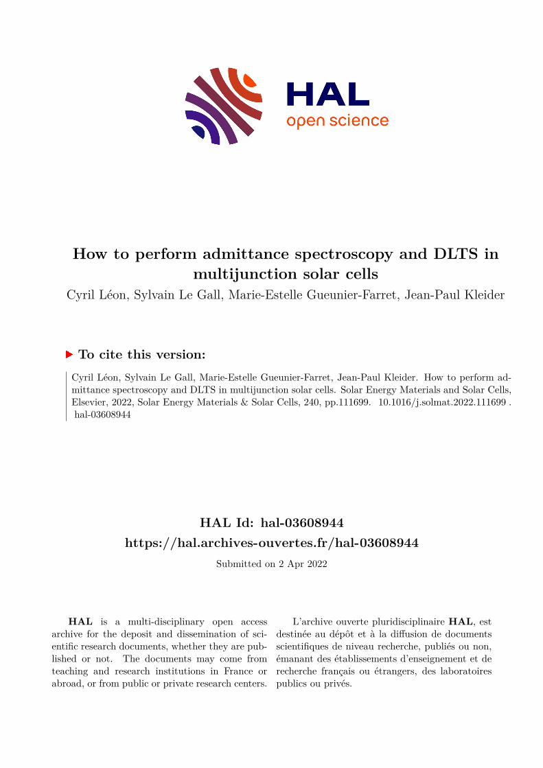
HAL Id: hal-03608944https://hal.archives-ouvertes.fr/hal-03608944
Submitted on 2 Apr 2022
HAL is a multi-disciplinary open accessarchive for the deposit and dissemination of sci-entific research documents, whether they are pub-lished or not. The documents may come fromteaching and research institutions in France orabroad, or from public or private research centers.
L’archive ouverte pluridisciplinaire HAL, estdestinée au dépôt et à la diffusion de documentsscientifiques de niveau recherche, publiés ou non,émanant des établissements d’enseignement et derecherche français ou étrangers, des laboratoirespublics ou privés.
How to perform admittance spectroscopy and DLTS inmultijunction solar cells
Cyril Léon, Sylvain Le Gall, Marie-Estelle Gueunier-Farret, Jean-Paul Kleider
To cite this version:Cyril Léon, Sylvain Le Gall, Marie-Estelle Gueunier-Farret, Jean-Paul Kleider. How to perform ad-mittance spectroscopy and DLTS in multijunction solar cells. Solar Energy Materials and Solar Cells,Elsevier, 2022, Solar Energy Materials & Solar Cells, 240, pp.111699. �10.1016/j.solmat.2022.111699�.�hal-03608944�

1
How to Perform Admittance Spectroscopy and DLTS in Multijunction Solar
Cells
Cyril Leon,1,2,3 Sylvain Le Gall,1,2,3 Marie-Estelle Gueunier-Farret,1,2,3 Jean-Paul Kleider1,2,3
1Université Paris-Saclay, CentraleSupélec, CNRS, Laboratoire de Génie Electrique et Electronique de
Paris, 91192, Gif-sur-Yvette, France. 2Sorbonne Université, CNRS, Laboratoire de Génie Electrique et Electronique de Paris, 75252, Paris,
France
3IPVF, Institut Photovoltaïque d’Ile-de-France, 91120, Palaiseau France
We propose a simple and non-destructive method to access the properties of
the defects within the subcells of multijunction solar cells (MJSC) based on
the extension of two well-known techniques, namely Admittance
Spectroscopy (AS) and Deep-Level Transient Spectroscopy (DLTS). Due to
the electrical coupling between the subcells of an MJSC, the AS and DLTS
signatures of the defects present in the subcells are difficult to identify and to
properly analyse, and other independent phenomena could be misinterpreted
as such. From numerical simulations and theoretical developments, it is
shown how the use of dedicated experimental conditions, in particular
specific light biases, on MJSCs can reveal the signatures of the defects present
in each subcell and allow one to analyse them without misinterpretation.
Keywords: Tandem Solar Cells, Multijunction Solar Cells, Admittance
Spectroscopy, Deep-Level Transient Spectroscopy, Electrical Coupling,
Modelling.
1. Introduction
Multijunction solar cells (MJSCs) offer the possibility to overcome the Shockley-Queisser
limit for a single junction solar cell and can reach efficiencies above 30% [1]. Among the best
MJSCs, performance records are achieved when several III-V materials subcells are combined:
39.2% for a six junction-solar cell, 38.8 % for a five-junction solar cell, 37.9 % for a triple-
junction solar cell and 32.8 % for a tandem solar cell (TSC) under 1-sun illumination [2-5].
Regarding the triple junctions and the tandem solar cells, technologies combining III-V and Si

2
materials also offer interesting efficiencies: 35.9 % et 32.8 % for cells associating three subcells
(GaInP/GaAs/Si) and two subcells (GaAs/Si), respectively [6]. In most cases, in a MJSC the
subcells are monolithically stacked and electrically coupled. This coupling results in difficulties
to characterize the MJSC at the subcell level which is important to optimize the fabrication
processes or understand the mechanism causing the degradation of the solar cells [7].
Admittance Spectroscopy (AS) and Deep-Level Transient Spectroscopy (DLTS) are two
well-known characterisation techniques that provide information on the defects causing
intermediate states in the bandgap energy of the materials [8-10]. Admittance spectroscopy
refers to the measurement as a function of frequency and temperature of the current in a device
submitted to a small alternative bias change, from which one can derive the equivalent parallel
junction capacitance, 𝐶𝐶, and parallel conductance 𝐺𝐺. DLTS uses the transient response of the
device following a voltage pulse and exploits the temperature dependence of the transient of
the current or of the junction capacitance. They have been widely used for solar cells
applications [11-31]. However, in MJSCs, the junctions and admittances of each subcell are
electrically (and optically) coupled, so that the response of the MJSC to a change in electrical
bias (either modulated or transient) has to be properly analysed in order to separate the
contribution of each subcell. Interestingly, while MJSCs have become one of the main target in
photovoltaics, only very few studies can be found in the literature that aim at developing
methods to separate the admittance (and thus the capacitance) of each subcell from the
measurement performed on the MJSC [32-35].
In a previous study, a method was proposed to separate the capacitance contributions of each
subcell within a TSC for the analysis of the capacitance-voltage technique, in order to access
the doping densities in the bases and the diffusion potential of each subcell independently [35].
In this article, on account of numerical modelling we demonstrate that this method can be
extended to the AS and DLTS characterisation techniques. As an example, we take a III-V/Si
TSC in which defects are introduced. First, the AS and DLTS results of the isolated subcells
are described and modelled. Then, we discuss the AS and DLTS results modelled from the
entire TSC in the dark in order to understand how the electrical coupling complicates the
analysis of the results. Next, the proposed method for separating the contributions of each
subcell is presented in more detail. Finally, information about the defects present in each subcell
of the modelled TSC is extracted by combining the proposed method with the AS and the DLTS
characterisation techniques.
2. Background

3
In this part, we give some theoretical reminders of the main capacitive effects in
semiconductor devices as well as some details on the principles of DLTS and AS techniques
before presenting the modeled structure.
2.1. Contributions to the admittance in a PN junction
When applying a small AC voltage bias signal at a given angular frequency, 𝜔𝜔, one can
measure the AC current and deduce the complex admittance, 𝑌𝑌 = 𝐺𝐺 + 𝑗𝑗𝐶𝐶𝜔𝜔, the real part
being the conductance 𝐺𝐺 and the imaginary part the susceptance 𝑗𝑗𝐶𝐶𝜔𝜔, 𝑗𝑗 being the complex
number such that 𝑗𝑗2 = −1 and 𝐶𝐶 the parallel capacitance. There are several contributions to
the admittance of a PN junction.
First, the presence of a depletion zone at the junction between the N and P regions causes a
so-called depletion-layer capacitance, 𝐶𝐶𝑤𝑤 [36]:
𝐶𝐶𝑤𝑤 = 𝜀𝜀𝑤𝑤
, (1)
𝑤𝑤 being to the width of the depletion layer and 𝜀𝜀 the dielectric permittivity of the material. In
the absence of deep-level defects, the width of the depletion layer only depends on the built-in
potential and on the doping densities in both N and P regions. However, in the presence of deep-
level defects in the bandgap of the material, 𝑤𝑤 will also depend on the defect concentrations. In
addition, the capture and emission of carriers by the defects can also contribute to the
capacitance of the PN junction. When applying a small AC voltage bias signal to measure the
admittance of a junction, two charge disturbances occur and contribute to the measured
admittance: one due to the modulation of the depletion width and another due to the variation
of the occupation of the defects. This latter disturbance depends on the response time of the
defect related to emission and capture of free carriers, 𝜏𝜏𝑇𝑇, and on the pulsation, 𝜔𝜔, of the small
AC bias signal. It has been shown that the junction conductance, 𝐺𝐺𝐽𝐽, and the junction
capacitance, 𝐶𝐶𝐽𝐽, in the presence of defects can then be written [37-39]:
𝐺𝐺𝐽𝐽𝜔𝜔
= Δ𝐶𝐶𝜔𝜔𝜏𝜏𝑇𝑇
1+𝜔𝜔2𝜏𝜏𝑇𝑇2 , (2)
and
𝐶𝐶𝐽𝐽 = 𝜀𝜀𝑤𝑤
+ Δ𝐶𝐶
1+𝜔𝜔2𝜏𝜏𝑇𝑇2 . (3)

4
with Δ𝐶𝐶 the contribution of the defects due to the variation of their occupation under quasi-
static conditions (𝜔𝜔𝜏𝜏𝑇𝑇 ≪ 1).
Second, the diffusion of free charge carriers across the junction causes a so-called diffusion
admittance of which the real part is the diffusion conductance, 𝐺𝐺𝐷𝐷, and the imaginary part is the
diffusion susceptance, 𝑗𝑗𝜔𝜔𝐶𝐶𝐷𝐷, 𝐶𝐶𝐷𝐷 being the diffusion capacitance. Sze calculated 𝐺𝐺𝐷𝐷 and 𝐶𝐶𝐷𝐷 for
a PN junction with semi-infinite materials, and he showed that both are related to the dark
current density, 𝐽𝐽𝑑𝑑𝑑𝑑𝑑𝑑𝑑𝑑 [36]. This can be extended in the case of solar cells based on an
asymmetric junction where the doping concentration of the emitter is much larger than that of
the base, introducing an effective lifetime of minority carriers in the base, 𝜏𝜏𝑒𝑒𝑒𝑒𝑒𝑒, with the
approximate expressions:
𝐺𝐺𝐷𝐷 = 𝑑𝑑𝐽𝐽𝑑𝑑𝑑𝑑𝑑𝑑𝑑𝑑𝑑𝑑𝑑𝑑 �1 + 𝜔𝜔𝜏𝜏𝑒𝑒𝑒𝑒𝑒𝑒 , (4)
and
𝐶𝐶𝐷𝐷 = 𝑑𝑑𝐽𝐽𝑑𝑑𝑑𝑑𝑑𝑑𝑑𝑑𝑑𝑑𝑑𝑑
× 𝜏𝜏𝑒𝑒𝑒𝑒𝑒𝑒�1+𝜔𝜔𝜏𝜏𝑒𝑒𝑒𝑒𝑒𝑒
, (5)
with V the applied DC voltage. Note that when 𝜔𝜔𝜏𝜏𝑒𝑒𝑒𝑒𝑒𝑒 ≪ 1, one can rewrite Eq. (4) and Eq. (5)
as the low-frequency diffusion conductance (𝐺𝐺𝐷𝐷,𝐿𝐿𝐿𝐿) and the low-frequency diffusion
capacitance (𝐶𝐶𝐷𝐷,𝐿𝐿𝐿𝐿):
𝐺𝐺𝐷𝐷,𝐿𝐿𝐿𝐿 = 𝑑𝑑𝐽𝐽𝑑𝑑𝑑𝑑𝑑𝑑𝑑𝑑𝑑𝑑𝑑𝑑
, (6)
and
𝐶𝐶𝐷𝐷,𝐿𝐿𝐿𝐿 = 𝑑𝑑𝐽𝐽𝑑𝑑𝑑𝑑𝑑𝑑𝑑𝑑𝑑𝑑𝑑𝑑
× 𝜏𝜏𝑒𝑒𝑒𝑒𝑒𝑒 . (7)
Usually, the diffusion capacitance is considered in forward bias where it becomes important
due to the exponential increase with DC bias, However, it exists whatever the bias and,
depending on material parameters, it cannot always be neglected even at zero or reverse bias.
The overall capacitance of the PN junction can be written:
𝐶𝐶 = 𝐶𝐶𝐽𝐽 + 𝐶𝐶𝐷𝐷 . (8)
Finally, the presence of a strong inversion layer at the interface of a PN junction can create
a so-called inversion-layer capacitance. Under certain conditions, this phenomenon can impact

5
the junction admittance especially for heterojunctions, and care has to be taken when analyzing
the admittance measurements of such devices [42]. However, this phenomenon has little impact
on the electrical coupling between the subcells of the MJSC. Therefore, to simplify this study
which aims at developing a method to overcome this coupling, the inversion-layer capacitance
will not be considered in the following.
2.2. Admittance Spectroscopy (AS)
The AS characterisation technique consists in measuring the admittance of the junction while
varying the frequency of the small AC bias excitation and the sample temperature. As shown
in the previous section, defects can contribute to the junction admittance and one can thus
exploit the temperature and/or the frequency dependence of either the conductance, 𝐺𝐺(𝑓𝑓,𝑇𝑇), or
the capacitance, 𝐶𝐶(𝑓𝑓,𝑇𝑇), to deduce the position of defect energy levels in the bandgap of the
base material. In practice however, the contribution of defects to the conductance is often
masked by the diffusion conductance and by a parasitic parallel conductance (related to shunts)
not taken into account in our analysis and which does not affect the capacitance. Therefore, we
will focus in the following on the capacitance only. From Eq. (3) one can deduce that the 𝐶𝐶(𝑓𝑓)
curve will follow an inflexion point at a frequency, 𝑓𝑓𝑖𝑖:
𝑓𝑓𝑖𝑖 = 12𝜋𝜋𝜏𝜏𝑇𝑇
. (9)
If we consider for example an electron trap (basically a trap located above midgap), it has
been shown that the change of occupancy of such defect is significant when its energy crosses
or is close to the electron quasi-Fermi level. At this point, the time response of the defect can
be written [8-10,38]:
𝜏𝜏𝑇𝑇 = 12𝑒𝑒𝑛𝑛
, (10)
with 𝑒𝑒𝑛𝑛 the emission frequency of the defect to the conduction band, which depends on the
difference between the energy position of the defect, 𝐸𝐸𝑇𝑇, and the energy of the receiving band,
𝐸𝐸𝐶𝐶, defined as the activation energy, 𝐸𝐸𝑑𝑑(𝐸𝐸𝑇𝑇) = 𝐸𝐸𝐶𝐶 − 𝐸𝐸𝑇𝑇 [8-10,37-41]:
𝑒𝑒𝑛𝑛(𝐸𝐸𝑇𝑇) = 𝜎𝜎𝑛𝑛𝑣𝑣𝑡𝑡ℎ,𝑛𝑛𝑁𝑁𝐶𝐶𝑒𝑒−𝐸𝐸𝑑𝑑(𝐸𝐸𝑇𝑇)𝑑𝑑𝐵𝐵𝑇𝑇 , (11)
with 𝜎𝜎𝑛𝑛 the capture cross section of electrons, 𝑣𝑣𝑡𝑡ℎ,𝑛𝑛 the thermal velocity of electrons, 𝑁𝑁𝐶𝐶 R the
effective density of states in the conduction band. For a hole trap, there are similar relations

6
with hole parameters instead of electron ones, and 𝐸𝐸𝑑𝑑(𝐸𝐸𝑇𝑇) = 𝐸𝐸𝑇𝑇 − 𝐸𝐸𝑑𝑑 and 𝐸𝐸𝑉𝑉 the top of the
valence band. By increasing the temperature of the sample, the emission rate of the electrons is
modified, and the inflexion point of the 𝐶𝐶(𝑓𝑓) curve occurs at a higher frequency. By
representing the frequencies of the inflexion points for several temperatures in an Arrhenius
plot, one can deduce the activation energy of the defect.
2.3. Deep-Level Transient Spectroscopy (DLTS)
There is a large number of modified techniques to perform Deep-Level Transient
Spectroscopy [41]. The classical DLTS characterisation technique proposed by D.V. Lang and
considered in this study consists in observing the transient evolution of the capacitance of a
junction for several temperatures, after having applied a positive voltage pulse (called filling
pulse) to deduce the energy level of the defect in the bandgap of the material, the defect
concentration and its capture cross section [8].
Generally, the sample is initially set under zero or reverse bias. The pulse amplitude is
chosen so that the junction is momentarily put under more positive bias to inject carriers into
the depletion zone. Thus, the probability of occupation changes: the electron traps in the
depletion zone are filled with electrons while the hole traps are filled with holes. After the pulse,
when the junction is again set under the initial bias, the captured charges are emitted and thus
the capacitance exhibits a transient and reaches its steady state value after a certain time related
to 𝜏𝜏𝑇𝑇. The variation of the capacitance after the pulse can be written [8,41]:
∆𝐶𝐶 = ∆𝐶𝐶0 × 𝑒𝑒−𝑡𝑡 𝜏𝜏𝑇𝑇⁄ , (12)
with ∆𝐶𝐶0 the variation of the capacitance just after the pulse. In the so-called and widely used boxcar technique, one measures the capacitance at two distinct
times in the transient, 𝑡𝑡1 and 𝑡𝑡2, at various temperatures. A DLTS spectrum, 𝑆𝑆(𝑇𝑇) is then defined
as 𝑆𝑆(𝑇𝑇) = 𝐶𝐶(𝑡𝑡1,𝑇𝑇) − 𝐶𝐶(𝑡𝑡2,𝑇𝑇). By varying the temperature of the sample, 𝜏𝜏𝑇𝑇 is modified. One
can show that 𝑆𝑆(𝑇𝑇) is maximum at the temperature 𝑇𝑇𝑖𝑖 where the emission frequency of the trap
level coincides with 𝑟𝑟 [8]:
𝑟𝑟 = ln(𝑡𝑡1/𝑡𝑡2)𝑡𝑡1−𝑡𝑡2
= 𝑒𝑒𝑛𝑛(𝑇𝑇 = 𝑇𝑇𝑖𝑖) , (13)
where 𝑟𝑟 is often called the window rate defined by 𝑡𝑡1 and 𝑡𝑡2. By repeating the measurements
for different window rates and tracking the maximum of 𝑆𝑆(𝑇𝑇) one can use an Arrhenius plot to
deduce the activation energy of the defect in a similar way as in admittance spectroscopy.

7
2.4. Presentation of the modelled structure
In this study, we take as an example a III-V/Si TSC. We modelled the subcells independently
using a TCAD software (Atlas from Silvaco©). This simulator solves the physical equations
governing the electrostatics (Poisson, electro-neutrality) and the transport of electrons and holes
(drift-diffusion) self-consistently on a 2D mesh [43]. The Top single cell is an AlGaAs NP
junction and the Bottom single cell is a c-Si NP junction as represented in Figs. 1(a) and (d),
respectively. Some information about the electrical input parameters of the various materials
can be found in the supplementary material. We then implement one single deep-defect state in
each cell, the properties of the defects are summarized in Table 1. To form the TSC, the two
subcells are electrically connected to each other. In practice, the intermediate layer allowing the
transport of charges between the Top and Bottom subcells of a 2T Tandem cell often consists
in a tunnel junction. Due to the high doping densities in the layers of the tunnel junction, its
capacitance can be neglected when considering the capacitance behavior of a 2T tandem device.
In order to greatly simplify the calculations, the tunnel junction is therefore replaced in our
models by a perfectly conductive intermediate layer, perfectly transparent and presenting no
potential barrier in contact with the Top and Bottom cells. In a previous study, the validity of
this simulated structure was experimentally verified by comparing the simulations with
admittance measurements performed on a device whose intermediate layer consists in a
classical tunnel junction [35].
Table 1. Properties of the deep defects implemented in the modelling of the Top and Bottom subcells. Defect properties Top cell
defect
Bottom cell
defect
𝐸𝐸𝑑𝑑 = 𝐸𝐸𝑇𝑇 − 𝐸𝐸𝑑𝑑 (eV) 0.5 0.4
𝑁𝑁𝑇𝑇 (cm-3) 1017 1015
𝜎𝜎𝑛𝑛 (cm2) 10−16 10−16
𝜎𝜎𝑝𝑝 (cm2) 10−16 10−16

8
3. Results and discussions
3.1. Modelling in the dark
In this part, we will start by presenting all the results of the AS and DLTS techniques modelled
on the subcells alone and on the TSC in the dark, highlighting the difficulty of extracting defect
parameters of the subcells from measurements performed in the dark on the TSC.
3.1.1. AS and DLTS results of the modelled cells
Figs. 1(b) and (e) show the 𝐶𝐶(𝑓𝑓,𝑇𝑇) curves of the modelled Top and Bottom single cells,
respectively, at 0 V DC when a small AC signal of 20 mV is applied. Figs. 1(c) and (f) represent
their respective DLTS spectra deduced from the modelled 𝐶𝐶(𝑡𝑡,𝑇𝑇) curves after a filling pulse
(from -1 V to 0 V then back to -1 V DC) is applied on the subcells alone. The window rates
taken to obtain the DLTS spectra are summarized in Table 2. By extracting the activation
energies from the AS and DLTS results of each subcell modelled alone, we successfully find
the activation energies of the defects implemented in our simulations.
Table 2. Window rates used to obtain the DLTS spectra from the 𝐶𝐶(𝑡𝑡,𝑇𝑇) curves. r1 (s-1) 2.6
r2 (s-1) 22.1
r3 (s-1) 117.1
r4 (s-1) 1761.2
Then we modelled the TSC by associating the Top and Bottom single cells in series. The
band diagram of the TSC is represented in Fig. 1(g). The energy levels of the defects are also
represented in Fig. 1(g) (𝐸𝐸𝑇𝑇1 R stands for the energy level of the defect in the Top while 𝐸𝐸𝑇𝑇2 R
stands for the one in the Bottom). The modelled 𝐶𝐶(𝑓𝑓,𝑇𝑇) curves at 0 V DC are represented in
Fig. 1(h) while the DLTS spectra are shown in Fig. 1(i). The AS and DLTS results of the
modelled TSC in the dark show two behaviours that could be related to the presence of defects:
Fig. 1(h) shows two different regions of inflexions of the 𝐶𝐶(𝑓𝑓,𝑇𝑇) curves while we can observe
two different regions of peaks in the DLTS spectra (Fig. 1(g)). From the first region, labelled
“A”, we find an activation energy that is either close (0.32 eV in the AS results) or equal (0.4
eV in the DLTS results) to the signature of the defect in the bottom cell. From the second region

9
of peaks and inflexions, labelled “B”, we extract an activation energy of 1 eV which does not
correspond to either of the two defects. In the next part, we explain the phenomena responsible
for the inflexion points in the AS results and peaks in the DLTS results in the A and B regions.
Fig. 1. Modelling results of the Top, Bottom and TSC cells. The top row corresponds to the Top cell: (a) sketch; (b) 𝐶𝐶(𝑓𝑓,𝑇𝑇) curves at 0 V DC, and (c) DLTS spectra. The middle row is dedicated to the Bottom cell: (d) sketch; (e) 𝐶𝐶(𝑓𝑓,𝑇𝑇) curves at 0 V DC, and (f) DLTS spectra. The bottom row is dedicated to the TSC: (g) energy band diagram; (h) 𝐶𝐶(𝑓𝑓,𝑇𝑇) curves at 0 V DC, and (i) DLTS spectra. The regions labelled by the “A” and “B” capital letter are discussed in the text.
3.1.2. Capacitance coupling and filling pulse distribution
Since the two subcells are connected in series, if we call 𝐶𝐶1 R the capacitance of the Top subcell
and 𝐶𝐶2 R the capacitance of the Bottom subcell, then the capacitance of the TSC, 𝐶𝐶𝑇𝑇𝑇𝑇𝐶𝐶, should be
equal to:
𝐶𝐶𝑇𝑇𝑇𝑇𝐶𝐶 = � 1𝐶𝐶1
+ 1𝐶𝐶2�−1
. (14)

10
In our case, where there is a large difference in doping between the bases of the subcells, one
can deduce that the capacitance behavior of the TSC will be close to the behavior of the subcell
whose base is the lowest doped. This justifies that the 𝐶𝐶(𝑓𝑓,𝑇𝑇) curves in region A in Fig. 1(h)
(TSC results) show a similar behavior as in Fig. 1(e) (Bottom cell results). However, because
of the capacitance coupling, the two results do not match, and it is not possible to extract with
precision the activation energy of the Bottom cell defects from TSC results. More details can
be found in the supplementary material section A.
For the DLTS characterisation technique, in addition to the capacitance coupling, one also
must consider the distribution of the filling pulse. The two capacitances of the subcells being
connected in series, the distribution of the voltage when applying a filling pulse, ∆𝑉𝑉𝑇𝑇𝑇𝑇𝐶𝐶, is:
�∆𝑉𝑉1 = ∆𝑉𝑉𝑇𝑇𝑇𝑇𝐶𝐶 × 𝐶𝐶2
𝐶𝐶1+𝐶𝐶2
∆𝑉𝑉2 = ∆𝑉𝑉𝑇𝑇𝑇𝑇𝐶𝐶 × 𝐶𝐶1𝐶𝐶1+𝐶𝐶2
, (15)
with ∆𝑉𝑉𝑇𝑇𝑇𝑇𝐶𝐶 the amplitude of the voltage pulse applied on the TSC, ∆𝑉𝑉1 the voltage change in
the Top subcell due to the applied pulse, and ∆𝑉𝑉2 the corresponding voltage change in the
Bottom subcell. If one makes the assumption that 𝐶𝐶1 and 𝐶𝐶2 are constant and simply by
considering the capacitance ranges (𝐶𝐶1 ~ 10−7 F. cm−2 and 𝐶𝐶2 ~ 10−8 F. cm−2), one can
deduce that almost 90 % of ∆𝑉𝑉𝑇𝑇𝑇𝑇𝐶𝐶 is actually applied on the Bottom subcell which is confirmed
by our modelling (see Fig. S3 from supplementary material section A).
In our case, one can deduce that almost only the defect in the Bottom subcell is probed when
performing DLTS on this TSC in the dark. This explains why the activation energy extracted
from the A region in Fig. 1(i) is equal to the activation energy of the defect in the Bottom
subcell. But this only stands for our particular case. In general, the filling pulse will mostly
apply on the subcell with the lowest capacitance, so in the dark, mostly this subcell can
eventually be probed by DLTS. But if the two capacitances are in the same range, results will
be more difficult to analyse. Moreover, in the following we show that diffusion also plays a
role and leads to artefacts regarding defects identification.
3.1.3. Diffusion phenomena
Capacitance coupling and voltage distribution explain well the behavior of the AS and DLTS
results in the A region of Figs. 1(h) and (i). Now, to understand the behavior in the B region,
we modelled the AS and DLTS curves of the TSC without defect (Figs. 2(a) and (b)). Here, we
can see that the defect signatures disappeared. However, the inflexion points in AS and the

11
unusual DLTS peaks observable in the B regions remain but occur at higher temperatures. This
means that the inflexions and peaks in the B regions of Figs. 1(h) and (i) are not related to the
presence of defects in the structure.
Fig. 2. (a) AS and (b) DLTS results of the TSC modelled in the dark without defect.
In fact, the increase of the temperature increases the saturation current density in the subcells.
This means, based on Eqs. (4) and (5), that the diffusion capacitance and the diffusion
conductance also increase with the temperature. In the case of subcell with high effective
lifetime material such as our c-Si Bottom subcell, diffusion capacitance and diffusion
conductance cannot be neglected at high temperature. This is verified indeed in the Bottom c-
Si subcell as shown in Fig. 3 where the real part of the admittance surpasses its imaginary part
above 375 K.
Fig. 3. Temperature dependence of the low-frequency capacitance and the low-frequency conductance divided by the pulsation of the small AC signal (at 20 Hz) in the modelled c-Si Bottom subcell without defect.

12
Consequently, we must consider the diffusion conductance and the diffusion capacitance of
the Bottom subcell to explain our results at high temperature. We note 𝐶𝐶𝑤𝑤,1 the depletion-layer
capacitance of the Top subcell, 𝐶𝐶𝑤𝑤,2, 𝐶𝐶𝐷𝐷,2 and 𝐺𝐺𝐷𝐷,2, the depletion-layer capacitance, diffusion
capacitance and diffusion conductance of the Bottom subcell, respectively. The equivalent
circuit of the TSC is now represented in Fig. 4.
Fig. 4. Simplified AC circuit of the TSC if we consider the contribution of diffusion phenomena in the bottom subcell. 𝐶𝐶𝑤𝑤,1 is the depletion-layer capacitance of the Top subcell, 𝐶𝐶𝑤𝑤,2, 𝐶𝐶𝐷𝐷,2 and 𝐺𝐺𝐷𝐷,2 are the depletion-layer capacitance, diffusion capacitance and diffusion conductance of the Bottom subcell, respectively.
The total capacitance of the Top subcell, 𝐶𝐶1 is equal to 𝐶𝐶𝑤𝑤,1; the total capacitance of the
Bottom subcell, 𝐶𝐶2 is equal to 𝐶𝐶𝑤𝑤,2 + 𝐶𝐶𝐷𝐷,2; the total conductance of the Bottom subcell, 𝐺𝐺2 is
equal to 𝐺𝐺𝐷𝐷,2. Therefore, the equivalent capacitance of the TSC is now:
𝐶𝐶𝑇𝑇𝑇𝑇𝐶𝐶 = 𝐶𝐶1 × 𝐶𝐶2𝐶𝐶1+𝐶𝐶2
×𝜔𝜔2+�𝐺𝐺2𝐶𝐶2
�2
× 𝐶𝐶2𝐶𝐶1+𝐶𝐶2
𝜔𝜔2+�𝐺𝐺2𝐶𝐶2�2
×� 𝐶𝐶2𝐶𝐶1+𝐶𝐶2
�2 . (16)
Based on this equation, one can deduce that the evolution of 𝐶𝐶𝑇𝑇𝑇𝑇𝐶𝐶 with frequency will follow a
first inflexion at a point where 𝜔𝜔 = 𝜔𝜔𝑇𝑇ℎ = 𝐺𝐺2√3(𝐶𝐶1+𝐶𝐶2)
. For lower frequencies, 𝐶𝐶𝑇𝑇𝑇𝑇𝐶𝐶 tends toward
𝐶𝐶1 (the bottom subcell is shunted) and for higher frequencies, 𝐶𝐶𝑇𝑇𝑇𝑇𝐶𝐶 tends toward
(1/𝐶𝐶1 + 1/𝐶𝐶2)−1 as it can be seen in Fig. 5(a). A second decrease occurs when the diffusion
capacitance in the Bottom subcell decreases with increasing frequency (see Eq. (5)) and the
position of this inflexion is noted 𝜔𝜔𝐻𝐻𝐿𝐿.
Considering the diffusion phenomena in the Bottom subcell, the distribution of the voltage
in the structure is modified:
⎩⎪⎨
⎪⎧∆𝑉𝑉1 = ∆𝑉𝑉𝑇𝑇𝑇𝑇𝐶𝐶 ×
1𝑗𝑗𝑗𝑗𝐶𝐶1
1𝑗𝑗𝑗𝑗𝐶𝐶2+𝐺𝐺2
+ 1𝑗𝑗𝑗𝑗𝐶𝐶1
∆𝑉𝑉2 = ∆𝑉𝑉𝑇𝑇𝑇𝑇𝐶𝐶 ×1
𝑗𝑗𝑗𝑗𝐶𝐶2+𝐺𝐺21
𝑗𝑗𝑗𝑗𝐶𝐶2+𝐺𝐺2+ 1𝑗𝑗𝑗𝑗𝐶𝐶1
. (17)

13
By assuming constant values of 𝐶𝐶1, 𝐶𝐶2 and 𝐺𝐺2 we can obtain the expression of the voltage
distribution in the subcells versus time after the filling pulse by writing Eq. (17) in the Laplace
domain, then by applying inverse Laplace transform:
�∆𝑉𝑉1 = ∆𝑉𝑉𝑇𝑇𝑇𝑇𝐶𝐶 × �1− 𝐶𝐶1
𝐶𝐶1+𝐶𝐶2𝑒𝑒−𝑡𝑡
𝐺𝐺2𝐶𝐶1+𝐶𝐶2�
∆𝑉𝑉2 = ∆𝑉𝑉𝑇𝑇𝑇𝑇𝐶𝐶 × 𝐶𝐶1𝐶𝐶1+𝐶𝐶2
𝑒𝑒−𝑡𝑡𝐺𝐺2
𝐶𝐶1+𝐶𝐶2 . (18)
This equation well describes the voltage distribution in our modelling (Fig. 5 (c)). Just before
the end of the pulse, 𝑉𝑉1 and 𝑉𝑉2 are equal to zero. At 𝑡𝑡 = 0, when ∆𝑉𝑉𝑇𝑇𝑇𝑇𝐶𝐶 = −1 V, simply by
considering the capacitance ranges and Eq. (18), one can deduce that almost 90 % of ∆𝑉𝑉𝑇𝑇𝑇𝑇𝐶𝐶 is
actually applied on the Bottom subcell. But as 𝑡𝑡 increases, 𝑉𝑉2 tends to reach back its initial value
(∆𝑉𝑉2 → 0) while all the pulse amplitude is applied on 𝑉𝑉1 (∆𝑉𝑉1 → ∆𝑉𝑉𝑇𝑇𝑇𝑇𝐶𝐶). However, in our
modelling, we can see that the evolution of the voltage distribution is indeed exponential when
the filling pulse is applied but not after it ended. This could be explained by resistive effects or
because we assumed 𝐶𝐶1, 𝐶𝐶2 and 𝐺𝐺2 as constant while they are actually voltage dependent and
thus evolve with time as can be seen on Fig. 5(b) [44]. This also induces a variation of 𝐶𝐶𝑇𝑇𝑇𝑇𝐶𝐶
after the pulse (Fig. 5(b)) which could be misinterpreted as the consequence of a defect. From
Eq. (18), we can notice that the characteristic time of the evolution of the voltage is 𝐶𝐶1+𝐶𝐶2𝐺𝐺2
, and
will be noted 𝑡𝑡𝑇𝑇ℎ to refer to 𝜔𝜔𝑇𝑇ℎ.
When increasing the temperature of the sample, the diffusion phenomena are more important
and thus change the values of 𝜔𝜔𝑇𝑇ℎ and 𝑡𝑡𝑇𝑇ℎ. 𝜔𝜔𝑇𝑇ℎ increases while 𝑡𝑡𝑇𝑇ℎ decreases with increasing
temperature which lead to the inflexions and peaks that can be seen in the B region of Fig. 1(h)
and (i). In fact, we can assume that the dependence of 𝜔𝜔𝑇𝑇ℎ and 𝑡𝑡𝑇𝑇ℎ on temperature follows the
dependence of 𝐺𝐺2 which is proportional to the dark current density of the silicon subcell. In first
approximation this is proportional to 𝑛𝑛𝑖𝑖2, 𝑛𝑛𝑖𝑖 being the intrinsic carrier concentration given by:
𝑛𝑛𝑖𝑖 = �𝑁𝑁𝐶𝐶𝑁𝑁𝑑𝑑 × 𝑒𝑒−𝐸𝐸𝑔𝑔
2𝑑𝑑𝐵𝐵𝑇𝑇� , (19)
with 𝐸𝐸𝑔𝑔 the gap of the material, 𝑁𝑁𝑑𝑑 and 𝑁𝑁𝐶𝐶 the effective density of states in the valence and
conduction bands, respectively.
This can explain the activation energy of ≈1 eV extracted from the Arrhenius plot of the
inflexions and peaks in the B region of Fig. 1(h) and (i) that reflect the bandgap energy of the
silicon material.

14
Fig. 5. (a) 𝐶𝐶(𝑓𝑓) curve modelled at 0 V DC and 440 K of the TSC, the Top and the Bottom subcells without defect, compared with the (1/𝐶𝐶1 + 1/𝐶𝐶2)−1 values; (b) 𝐶𝐶(𝑡𝑡) curve modelled at 390 K of the TSC, the Top and the Bottom subcells without defect, compared with the (1/𝐶𝐶1 + 1/𝐶𝐶2)−1 value after the filling pulse; (c) The evolution of the voltage distribution between the subcells of the TSC without defect.
To conclude this part, utilizing AS and DLTS characterisation techniques on the TSC in the
dark can lead to misinterpretation of the results. First, due to the electrical coupling, the defects
signatures are mixed. If the capacitance of one of the subcells is important enough, then only
the defect signatures of the other subcell might be observable but due to the coupling, the
extraction of their properties might lead to errors. Regarding the DLTS characterisation
technique, additional consideration should be given to the distribution of the filling pulse
applied on the structure. If, as it is the case in this study, the filling pulse is mostly applied on
one of the two subcells, then only this one is probed. Second, the impact of the diffusion
phenomena can be mixed with the signature of a defect or can lead to an AS and DLTS signature
that can be improperly attributed to the existence of a defect that does not exist. The impact of
those phenomena and of the capacitance- and voltage coupling strongly depend on the studied
structure. Each technology might behave differently. Therefore, in the dark, it seems very
difficult to properly analyse AS or DLTS results without a strong support from complementary
modelling.
In the following, we propose a simple and non-destructive method allowing (i) to decouple
the capacitances, (ii) to know and control how the voltage is shared between the subcells, (iii)

15
to know which subcell is probed and (iv) to ensure that the diffusion phenomena cannot be
confused with the defect signatures anymore.
3.2. Proposed light bias method
3.2.1. Overcoming the electrical coupling: use of light biases
The proposed method uses a light bias whose wavelength is such that it can be absorbed only
by one of the subcells in the TSC. This results in fixing the polarization of the absorbing subcell
near its open-circuit voltage if the applied voltage on the TSC is reverse or slightly direct (below
the open-circuit voltage value of the absorbing subcell). In that way we can control in which
subcell the diffusion phenomena are important since those mostly occur in the direct polarized
subcell, i.e. the absorbing subcell. More details can be found in Ref. [35,44]. We use K as the
index of the subcell in the dark and L as the index of the other subcell that absorbs the light.
Then, Eqs. (16) and (18) become:
𝐶𝐶𝑇𝑇𝑇𝑇𝐶𝐶 = 𝐶𝐶𝐾𝐾 × 𝐶𝐶𝐿𝐿𝐶𝐶𝐾𝐾+𝐶𝐶𝐿𝐿
×𝜔𝜔2+�𝐺𝐺𝐿𝐿𝐶𝐶𝐿𝐿
�2
× 𝐶𝐶𝐿𝐿𝐶𝐶𝐾𝐾+𝐶𝐶𝐿𝐿
𝜔𝜔2+�𝐺𝐺𝐿𝐿𝐶𝐶𝐿𝐿�2
×� 𝐶𝐶𝐿𝐿𝐶𝐶𝐾𝐾+𝐶𝐶𝐿𝐿
�2 , (20)
and
⎩⎪⎨
⎪⎧ ∆𝑉𝑉𝐿𝐿 = ∆𝑉𝑉𝑇𝑇𝑇𝑇𝐶𝐶 × 𝐶𝐶𝐾𝐾
𝐶𝐶𝐾𝐾+𝐶𝐶𝐿𝐿𝑒𝑒−𝑡𝑡
𝐺𝐺𝐿𝐿𝐶𝐶𝐾𝐾+𝐶𝐶𝐿𝐿
∆𝑉𝑉𝐾𝐾 = ∆𝑉𝑉𝑇𝑇𝑇𝑇𝐶𝐶 × �1 − 𝐶𝐶𝐾𝐾𝐶𝐶𝐾𝐾+𝐶𝐶𝐿𝐿
𝑒𝑒−𝑡𝑡𝐺𝐺𝐿𝐿
𝐶𝐶𝐾𝐾+𝐶𝐶𝐿𝐿� . (21)
Also, 𝜔𝜔𝑇𝑇ℎ becomes 𝐺𝐺𝐿𝐿√3(𝐶𝐶𝐾𝐾+𝐶𝐶𝐿𝐿)
and 𝑡𝑡𝑇𝑇ℎ becomes 𝐶𝐶𝐾𝐾+𝐶𝐶𝐿𝐿𝐺𝐺𝐿𝐿
.
First, from Eq. (20), we can deduce that for 𝜔𝜔 < 𝜔𝜔𝑇𝑇ℎ, 𝐶𝐶𝑇𝑇𝑇𝑇𝐶𝐶 tends toward 𝐶𝐶𝐾𝐾. Unlike the case
of the TSC in the dark, here we can choose which subcell is shunted at low frequency and only
obtain the capacitance of the subcell in the dark by adapting the wavelength of the light bias.
For example, with a 405 nm light bias fully absorbed in the Top subcell (this case is referred to
as TSC405), for pulsation below 𝜔𝜔𝑇𝑇ℎ one can probe only the Bottom subcell (see Fig. 6(a)) while
with a 980 nm light bias fully absorbed in the Bottom subcell (this case is referred to as TSC980),
one can probe only the Top subcell (see Fig. 6(b)). Second, since the absorbing subcell is
polarized in direct while the other subcell is polarized in reverse, we know that 𝐶𝐶𝐿𝐿 ≫ 𝐶𝐶𝐾𝐾. Based
on Eq. (21), we can assume that when a voltage step is applied on the TSC, only a little fraction
of it will occur in the absorbing subcell. For example, in the TSC405 case, the filling pulse

16
applied on the TSC mostly occurs in the Bottom subcell (see Fig. 7(a)) while the Top subcell is
polarized at its open-circuit voltage value. In the opposite, in the TSC980 case, the filling pulse
applied on the TSC mostly occurs in the Top subcell (see Fig. 7(b)) while the Bottom subcell
is polarized at its open-circuit voltage value.
Fig. 6. 𝐶𝐶(𝑓𝑓) curves modelled at 300 K from (a) the TSC, the Bottom subcell and (1/𝐶𝐶1 + 1/𝐶𝐶2)−1 in the TSC405 case without defects under 1 mW.cm-2 light bias and (b) the TSC, the Top subcell and (1/𝐶𝐶1 + 1/𝐶𝐶2)−1 in the TSC980 case without defects under 1 mW.cm-2 light bias.
Fig. 7. Distribution of the applied voltage between the subcells versus time (a) in the TSC405 case and (b) in the TSC980 case at 300 K under 1 W.cm-2 light bias.
This method allows to choose which subcell is probed. However, there are still inflexions in the
𝐶𝐶(𝑓𝑓) curves and transient evolutions of the voltage distribution. In the previous section, we
have shown that in the dark, the position of the inflexions and the characteristic times of the
transient evolution are temperature dependent and disturb the observation of the defect

17
signatures. Thus, in the following, we are going to demonstrate that when the TSC is under
specific illumination, 𝜔𝜔𝑇𝑇ℎ and 𝑡𝑡𝑇𝑇ℎ can be easily distinguished from the defect signatures.
3.2.2. Distinguishing the defects signatures from diffusion phenomena
Unlike the case were the TSC is in the dark, when one of the two subcells fully absorbs the
light, the modelling shows negligible dependency of 𝜔𝜔𝑇𝑇ℎ and 𝑡𝑡𝑇𝑇ℎ with temperature (see
supplementary material section B). In fact, when the DC voltage applied on the TSC is reverse
or zero and when one of the two subcells absorbs the light, the current flowing through the TSC
is close to zero. This implies that within the absorbing subcell, the photogenerated current, 𝐽𝐽𝑝𝑝ℎ,
is compensated by the dark current density (𝐽𝐽𝑝𝑝ℎ = 𝐽𝐽𝑑𝑑𝑑𝑑𝑑𝑑𝑑𝑑). Eqs. (4) and (5) become:
𝐺𝐺𝐷𝐷 = 𝑞𝑞𝐽𝐽𝑝𝑝ℎ𝑑𝑑𝐵𝐵𝑇𝑇
�1 + 𝜔𝜔𝜏𝜏𝑒𝑒𝑒𝑒𝑒𝑒 , (22)
and
𝐶𝐶𝐷𝐷 = 𝑞𝑞𝐽𝐽𝑝𝑝ℎ𝑑𝑑𝐵𝐵𝑇𝑇
× 𝜏𝜏𝑒𝑒𝑒𝑒𝑒𝑒�1+𝜔𝜔𝜏𝜏𝑒𝑒𝑒𝑒𝑒𝑒
, (23)
The photogenerated current being, at first order, independent of the temperature, it means
that under such illumination condition, the temperature dependence of the diffusion capacitance
and conductance can be neglected as well as the temperature dependence of 𝜔𝜔𝑇𝑇ℎ and 𝑡𝑡𝑇𝑇ℎ. (see
Fig. S4 and Fig. S5 from supplementary material section B).
On another hand, this also means that we can tune their values by changing the intensity of
the light biases to modify the value of the photogenerated current in the absorbing subcell. By
choosing a photon flux important enough, one can shift 𝜔𝜔𝑇𝑇ℎ toward high frequency such as one
can observe the AS results of the subcell in the dark over the entire considered frequency range.
Also, one can decrease 𝑡𝑡𝑇𝑇ℎ so that it is outside the time windows considered when performing
DLTS analyses and one can thus observe the defect signature of the subcell in the dark. More
details can be found in the supplementary material.
3.2.3. AS and DLTS combined with light biases: extracting the defect properties of each
subcell
On Fig. 8(b) and (d), we represent the modelled 𝐶𝐶(𝑓𝑓,𝑇𝑇) curves and DLTS spectra of the
TSC405 under an illumination of 1 W.cm-2 (high enough such that 𝜔𝜔𝑇𝑇ℎ is outside the considered
frequency range and 𝑡𝑡𝑇𝑇ℎ is outside the time windows used for DLTS analysis). In order to
18
compare the AS and DLTS results of the TSC405 with those of the Bottom subcell alone (Figs.
8(a) and (c)), we make sure that they are in the same polarization conditions. We have shown
that in order to do so, one needs to add the open-circuit voltage of the Top subcell to the
polarization of the TSC405 [35].
Fig. 8. (a) AS results of the Bottom subcell modelled alone at 0 V DC; (b) AS results of the TSC405 under a light power density of 1 W.cm-2 and polarized at the open-circuit value of the absorbing Top subcell; (c) DLTS results of the Bottom subcell modelled alone; (d) DLTS results of the TSC405 under a light power density of 1 W.cm-2.
In both AS and DLTS, we notice that, we obtain exactly the same figures whether the
modelling was carried out on the Bottom cell alone or on the TSC405. The same activation
energy can be extracted in both cases and corresponds to the activation energy of the defect
implemented in our modelling. The inflexion points and the unusual DLTS peaks observable in
the B region of the modelling results in the dark are not observable when the TSC is under the
405 nm light bias as previously discussed in Section 3.2.2 so that only the signature of the defect
in the subcell in the dark can be seen.
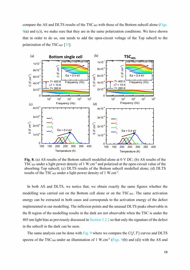
The same analysis can be done with Fig. 9 where we compare the 𝐶𝐶(𝑓𝑓,𝑇𝑇) curves and DLTS
spectra of the TSC980 under an illumination of 1 W.cm-2 (Figs. 9(b) and (d)) with the AS and
19
DLTS results of the Top subcell alone (Figs. 9(a) and (c)). Under the 980 nm light bias, we can
clearly see only the contribution of the defect in the Top subcell which was not observable when
the modelling was performed on the TSC in the dark.
Fig. 9. (a) AS results of the Top subcell modelled alone at 0 V DC; (b) AS results of the TSC980 under a light power density of 1 W.cm-2 and polarized at the open-circuit value of the Bottom subcell; (c) DLTS results of the Top subcell modelled alone; (d) DLTS results of the TSC980 under a light power density of 1 W.cm-2.
The high frequency drops of the curves in Fig. 9(b) are due to the decrease of the bottom
subcell capacitance with increasing frequency. In fact, at such high frequency (compared to the
inverse of the effective minority carrier lifetime of the absorbing subcell) the method encounters
some limitations. Indeed, the diffusion capacitance and conductance of the absorbing subcell,
𝐶𝐶𝐷𝐷,𝐿𝐿 and 𝐺𝐺𝐷𝐷,𝐿𝐿 (Eqs. (4) and (5)) become frequency dependent, and so also does 𝜔𝜔𝑠𝑠ℎ. The
capacitances are not decoupled anymore (for frequency higher than 104 Hz) but with a photon
flux high enough, the capacitance of the absorbing subcell is so important that it can still be
negligible in 𝐶𝐶𝑇𝑇𝑇𝑇𝐶𝐶 until the drop of 𝐶𝐶𝐷𝐷,𝐿𝐿 with increasing frequency becomes too important (for

20
frequencies higher than 105 Hz). When increasing the temperature, this point happens at a
slightly lower frequency because of the temperature dependence of 𝐶𝐶𝐷𝐷,𝐿𝐿.
4. Conclusion
We have described a method to access the defects properties in each subcell within a TSC by
combining AS and DLTS characterisation techniques with the use of specific light biases.
Without such light biases, if the TSC is in the dark, the defect signatures of each subcell can be
coupled and depending on the materials and defect properties, the AS and DLTS signals of one
of the subcells can prevail. In addition, it has been shown that the increase of the diffusion
phenomena with temperature in one of the subcells can have an impact on the AS and DLTS
signals. Very importantly, it can lead to artefacts in AS and DLTS that can be misinterpreted as
the signature of a defect.
Using analytical and numerical modelling approaches, we have shown that the use of specific
light biases such that the subcell of interest is in the dark while the other fully absorbs the light,
allows to “choose” in which subcell the diffusion phenomena mostly occur: the absorbing
subcell. This causes the shunt of the capacitance of the absorbing subcell at low frequency and
ensures that a filling pulse will be mostly applied in the subcell in the dark. Therefore, the use
of light biases allows to choose, both in AS and DLTS characterisation techniques, which
subcell is probed. The use of light biases also changes the dependency of the diffusion
phenomena with temperature which can be more easily distinguished from the defect
signatures. Also, by adjusting the power densities of the light biases the impact of the diffusion
phenomena on the AS and DLTS signals can be shifted out of the considered frequency range
and time windows such that the obtained signals can be equal to those of the subcells alone.
This simple and non-destructive method could easily be extended to MJSCs consisting of more
than two subcells by ensuring that each subcell in the MJSC is light-biased, except the one that
is to be probed.
5. References
[1] W. Shockley, H.J. Queisser, Detailed Balance Limit of Efficiency of p‐n Junction Solar Cells, J. Appl. Phys. 32 (1961) 510. https://doi.org/10.1063/1.1736034.
[2] J.F. Geisz, M.A. Steiner, N. Jain, K.L. Schulte, R.M. France, W.E. McMahon, E.E. Perl, D.J. Friedman, Building a Six-Junction Inverted Metamorphic Concentrator Solar Cell. IEEE J. Photovoltaics 8 (2018) 626.

21
[3] P.T. Chiu, D.C. Law, R.L. Woo, S.B. Singer, D. Bhusari, W.D. Hong, A. Zakaria, J. Boisvert, S. Mesropian, R.R. King, N.H. Karam, 35.8% space and 38.8% terrestrial 5J direct bonded cells, 2014 IEEE 40th Photovolt. Spec. Conf. PVSC 2014. (2014) 11–13. https://doi.org/10.1109/PVSC.2014.6924957.
[4] K. Sasaki, T. Agui, K. Nakaido, N. Takahashi, R. Onitsuka, T. Takamoto, Development of InGaP/GaAs/InGaAs inverted triple junction concentrator solar cells, AIP Conf. Proc. 1556 (2013) 22. https://doi.org/10.1063/1.4822190.
[5] M.A. Green, E.D. Dunlop, D.H. Levi, J. Hohl-Ebinger, M. Yoshita, A.W.Y. Ho-Baillie, Solar cell efficiency tables (version 54), Prog. Photovoltaics Res. Appl. 27 (2019) 565–575. https://doi.org/10.1002/PIP.3171.
[6] S. Essig, C. Allebé, T. Remo, J.F. Geisz, M.A. Steiner, K. Horowitz, L. Barraud, J.S. Ward, M. Schnabel, A. Descoeudres, D.L. Young, M. Woodhouse, M. Despeisse, C. Ballif, A. Tamboli, Raising the one-sun conversion efficiency of III–V/Si solar cells to 32.8% for two junctions and 35.9% for three junctions, Nat. Energy 2017 29. 2 (2017) 1–9. https://doi.org/10.1038/nenergy.2017.144.
[7] M. Meusel, C. Baur, G. Siefer, F. Dimroth, A.W. Bett, W. Warta, Characterization of monolithic III–V multi-junction solar cells—challenges and application, Sol. Energy Mater. Sol. Cells. 90 (2006) 3268–3275. https://doi.org/10.1016/J.SOLMAT.2006.06.025.
[8] D. V. Lang, Deep‐level transient spectroscopy: A new method to characterize traps in semiconductors, J. Appl. Phys. 45 (1974) 3023. https://doi.org/10.1063/1.1663719.
[9] D.L. Losee, Admittance spectroscopy of deep impurity levels: ZnTe Schottky barriers, Appl. Phys. Lett. 21 (1972) 54. https://doi.org/10.1063/1.1654276.
[10] D.L. Losee, Admittance spectroscopy of impurity levels in Schottky barriers, J. Appl. Phys. 46 (1975) 2204. https://doi.org/10.1063/1.321865.
[11] A. Ali, T. Gouveas, M.A. Hasan, S.H. Zaidi, M. Asghar, Influence of deep level defects on the performance of crystalline silicon solar cells: Experimental and simulation study, Sol. Energy Mater. Sol. Cells. 95 (2011) 2805–2810. https://doi.org/10.1016/j.solmat.2011.05.032.
[12] A.I. Baranov, A.S. Gudovskikh, A.Y. Egorov, D.A. Kudryashov, S. Le Gall, J.P. Kleider, Defect properties of solar cells with layers of GaP based dilute nitrides grown by molecular beam epitaxy, J. Appl. Phys. 128 (2020) 023105. https://doi.org/10.1063/1.5134681.
[13] A.I. Baranov, A.S. Gudovskikh, D.A. Kudryashov, A.A. Lazarenko, I.A. Morozov, A.M. Mozharov, E. V. Nikitina, E. V. Pirogov, M.S. Sobolev, K.S. Zelentsov, A.Y. Egorov, A. Darga, S. Le Gall, J.P. Kleider, Defect properties of InGaAsN layers grown as sub-monolayer digital alloys by molecular beam epitaxy, J. Appl. Phys. 123 (2018) 161418. https://doi.org/10.1063/1.5011371.

22
[14] M. Burgelman, P. Nollet, Admittance spectroscopy of thin film solar cells, Solid State Ionics. 176 (2005) 2171–2175. https://doi.org/10.1016/j.ssi.2004.08.048.
[15] J. Chantana, D. Hironiwa, T. Watanabe, S. Teraji, T. Minemoto, Flexible Cu(In,Ga)Se-2 solar cell on stainless steel substrate deposited by multi-layer precursor method: its photovoltaic performance and deep-level defects, Prog. Photovoltaics Res. Appl. 24 (2016) 990–1000. https://doi.org/10.1002/pip.2748.
[16] Y.C. Choi, D.U. Lee, J.H. Noh, E.K. Kim, S. Il Seok, Highly improved Sb2S3 sensitized-inorganic-organic heterojunction solar cells and quantification of traps by deep-level transient spectroscopy, Adv. Funct. Mater. 24 (2014) 3587–3592. https://doi.org/10.1002/adfm.201304238.
[17] Z. Djebbour, A. Darga, A. Migan Dubois, D. Mencaraglia, N. Naghavi, J.F. Guillemoles, D. Lincot, Admittance spectroscopy of cadmium free CIGS solar cells heterointerfaces, Thin Solid Films. 511–512 (2006) 320–324. https://doi.org/10.1016/j.tsf.2005.11.087.
[18] T. Eisenbarth, T. Unold, R. Caballero, C.A. Kaufmann, H.W. Schock, Interpretation of admittance, capacitance-voltage, and current-voltage signatures in Cu(In,Ga)Se2 thin film solar cells, J. Appl. Phys. 107 (2010) 0–12. https://doi.org/10.1063/1.3277043.
[19] M. González, A.M. Carlin, C.L. Dohrman, E.A. Fitzgerald, S.A. Ringel, Determination of bandgap states in p-type In0.49Ga 0.51P grown on SiGe/Si and GaAs by deep level optical spectroscopy and deep level transient spectroscopy, J. Appl. Phys. 109 (2011) 0–7. https://doi.org/10.1063/1.3559739.
[20] A.S. Gudovskikh, J.P. Kleider, R. Chouffot, N.A. Kalyuzhnyy, S.A. Mintairov, V.M. Lantratov, III-phosphides heterojunction solar cell interface properties from admittance spectroscopy, J. Phys. D. Appl. Phys. 42 (2009) 165307. https://doi.org/10.1088/0022-3727/42/16/165307.
[21] A.S. Gudovskikh, J.P. Kleider, J. Damon-Lacoste, P. Roca i Cabarrocas, Y. Veschetti, J.C. Muller, P.J. Ribeyron, E. Rolland, Interface properties of a-Si:H/c-Si heterojunction solar cells from admittance spectroscopy, Thin Solid Films. 511–512 (2006) 385–389. https://doi.org/10.1016/j.tsf.2005.12.111.
[22] S. Heo, G. Seo, Y. Lee, D. Lee, M. Seol, J. Lee, J.B. Park, K. Kim, D.J. Yun, Y.S. Kim, J.K. Shin, T.K. Ahn, M.K. Nazeeruddin, Deep level trapped defect analysis in CH3NH3PbI3 perovskite solar cells by deep level transient spectroscopy, Energy Environ. Sci. 10 (2017) 1128–1133. https://doi.org/10.1039/c7ee00303j.
[23] X. Hu, J. Tao, G. Weng, J. Jiang, S. Chen, Z. Zhu, J. Chu, Investigation of electrically-active defects in Sb2Se3 thin-film solar cells with up to 5.91% efficiency via admittance spectroscopy, Sol. Energy Mater. Sol. Cells. 186 (2018) 324–329. https://doi.org/10.1016/j.solmat.2018.07.004.
[24] M. Jiang, F. Lan, B. Zhao, Q. Tao, J. Wu, D. Gao, G. Li, Observation of lower defect density in CH3NH3Pb(I,Cl)3 solar cells by admittance spectroscopy, Appl. Phys. Lett. 108 (2016) 243505. https://doi.org/10.1063/1.4953834.

23
[25] J. Lauwaert, L. Van Puyvelde, J. Lauwaert, J.W. Thybaut, S. Khelifi, M. Burgelman, F. Pianezzi, A.N. Tiwari, H. Vrielinck, Assignment of capacitance spectroscopy signals of CIGS solar cells to effects of non-ohmic contacts, Sol. Energy Mater. Sol. Cells. 112 (2013) 78–83. https://doi.org/10.1016/J.SOLMAT.2013.01.014.
[26] H.S. Lee, M. Yamaguchi, N.J. Ekins-Daukes, A. Khan, T. Takamoto, T. Agui, K. Kamimura, M. Kaneiwa, M. Imaizumi, T. Ohshima, H. Itoh, Deep-level defects introduced by 1 MeV electron radiation in AlInGaP for multijunction space solar cells, J. Appl. Phys. 98 (2005) 1–5. https://doi.org/10.1063/1.2115095.
[27] J. Li, S.Y. Kim, D. Nam, X. Liu, J.H. Kim, H. Cheong, W. Liu, H. Li, Y. Sun, Y. Zhang, Tailoring the defects and carrier density for beyond 10% efficient CZTSe thin film solar cells, Sol. Energy Mater. Sol. Cells. 159 (2017) 447–455. https://doi.org/10.1016/J.SOLMAT.2016.09.034.
[28] J. Li, X. Yu, S. Yuan, L. Yang, Z. Liu, D. Yang, Effects of oxygen related thermal donors on the performance of silicon heterojunction solar cells, Sol. Energy Mater. Sol. Cells. 179 (2018) 17–21. https://doi.org/10.1016/J.SOLMAT.2018.02.006.
[29] M.A. Lourenço, Y.K. Yew, K.P. Homewood, K. Durose, H. Richter, D. Bonnet, Deep level transient spectroscopy of CdS/CdTe thin film solar cells, J. Appl. Phys. 82 (1997) 1423–1426. https://doi.org/10.1063/1.366285.
[30] I. Rimmaudo, A. Salavei, E. Artegiani, D. Menossi, M. Giarola, G. Mariotto, A. Gasparotto, A. Romeo, Improved stability of CdTe solar cells by absorber surface etching, Sol. Energy Mater. Sol. Cells. 162 (2017) 127–133. https://doi.org/10.1016/J.SOLMAT.2016.12.044.
[31] A.S. Shikoh, S. Paek, A.Y. Polyakov, N.B. Smirnov, I. V. Shchemerov, D.S. Saranin, S.I. Didenko, Z. Ahmad, F. Touati, M.K. Nazeeruddin, Assessing mobile ions contributions to admittance spectra and current-voltage characteristics of 3D and 2D/3D perovskite solar cells, Sol. Energy Mater. Sol. Cells. 215 (2020) 110670. https://doi.org/10.1016/J.SOLMAT.2020.110670.
[32] C.M. Ruiz, I. Rey-Stolle, I. Garcia, E. Barrigón, P. Espinet, V. Bermúdez, C. Algora, Capacitance measurements for subcell characterization in multijunction solar cells, Conf. Rec. IEEE Photovolt. Spec. Conf. (2010) 708–711. https://doi.org/10.1109/PVSC.2010.5617045.
[33] M. Rutzinger, M. Salzberger, A. Gerhard, H. Nesswetter, P. Lugli, C.G. Zimmermann, Measurement of subcell depletion layer capacitances in multijunction solar cells, Appl. Phys. Lett. 111 (2017) 183507. https://doi.org/10.1063/1.4998148.
[34] X. Zhang, J. Hu, Y. Wu, and F. Lu, Direct observation of defects in triple-junction solar cell by optical deep-level transient spectroscopy, J. Phys. D: Appl. Phys. 42 (2009) 145401. https://doi.org/10.1088/0022-3727/42/14/145401
[35] C. Leon, S. Le Gall, M.-E. Gueunier-Farret, A. Brézard-Oudot, A. Jaffre, N. Moron, L. Vauche, K. Medjoubi, E.V. Vidal, C. Longeaud, J.-P. Kleider, Understanding and monitoring the capacitance-voltage technique for the characterization of tandem solar

24
cells, Prog. Photovoltaics Res. Appl. 28 (2020) 601–608. https://doi.org/10.1002/PIP.3235.
[36] S.M. Sze, Physics of Semiconductor Devices, volume 23. Wiley-Interscience, Murray Hill, New Jersey, 2nd edition, 1981.
[37] W.G. Oldham, S.S. Naik, Admittance of p-n Junctions Containing Traps, Solid-state Electronics 15 (1972) 1085-1096. https://doi.org/10.1016/0038-1101(72)90167-0.
[38] C. Ghezzi, Space-Charge Analysis for the Admittance of Semiconductor Junctions with Deep Impurity Levels, Appl. Phys. A 26 (1981) 191-202. https://doi.org/10.1007/BF00614756.
[39] J.L. Pautrat, B. Katircioglu, N. Magnea, D. Bensahel, J.C. Pfister, L. Revoil, Admittance spectroscopy: A powerful characterization technique for semiconductor crystals—Application to ZnTe, Solid. State. Electron. 23 (1980) 1159–1169. https://doi.org/10.1016/0038-1101(80)90028-3.
[40] W. Shockley, J. W. T. Read, Statistics of the Recombinations of Holes and Electrons, Phys. Rev. 87 (1952) 835. https://doi.org/10.1103/PhysRev.87.835.
[41] A.R. Peaker, V.P. Markevich, J. Coutinho, Tutorial: Junction spectroscopy techniques and deep-level defects in semiconductors, J. Appl. Phys. 123 (2018) 161559. https://doi.org/10.1063/1.5011327.
[42] J.-P. Kleider, J. Alvarez, A. Brézard-Oudot, M.-E. Gueunier-Farret, O. Maslova, Revisiting the theory and usage of junction capacitance: Application to high efficiency amorphous/crystalline silicon heterojunction solar cells, Sol. Energy Mater. Sol. Cells. 135 (2015) 8–16 https://doi.org/10.1016/j.solmat.2014.09.002.
[43] Silvaco. Atlas User’s Manual 2016.
[44] C. Leon. Adaptation des techniques de caractérisation basées sur des mesures de capacité et d’admittance aux cellules solaires multijonctions : expériences et modélisations. Energie électrique. Université Paris-Saclay. 2020. Français.
Copyright © 2022 FDOKUMEN