High mobility short-channel p-type organic transistors with reduced gold content and completely...
9
High mobility short-channel p-type organic transistors with reduced gold content and completely gold-free source/drain bottom contacts R. Müller a,⇑ , S. Smout a , C. Rolin a , J. Genoe a , P. Heremans a,b a IMEC, Large Area Electronics – Polymer and Molecular Electronics, Kapeldreef 75, Leuven B-3001, Belgium b ESAT, Katholieke Universiteit Leuven, Kasteelpark Arenberg 10, B-3001 Leuven, Belgium article info Article history: Received 1 February 2011 Received in revised form 21 March 2011 Accepted 23 March 2011 Available online 8 April 2011 Keywords: Pentacene Bottom contact Low-cost Palladium Aluminum Short channel transistor abstract Pure gold layers are traditionally used for the fabrication of source/drain bottom contacts of high performance short channel pentacene transistors. In this work, these layers are suc- cessfully replaced by low cost metallic bilayers, consisting of a thick aluminum layer with a good electrical conductivity covered by a thin noble metal layer (gold or palladium) provid- ing good charge injection into the organic semiconductor. Corresponding pentacene tran- sistors with 5 lm channel length achieve saturation mobilities in the range of 0.4–0.5 cm 2 / (V s), comparable to those of reference pentacene transistors based on 30 nm thick pure gold bottom contacts, but for a metal cost down to 5% of that of the reference transistors. Ó 2011 Elsevier B.V. All rights reserved. 1. Introduction During the past decades organic electronics has evolved from a laboratory curiosity towards a technology for highly innovative products based for example on large-area flexi- ble electronic circuits [1–7]. A major driving force for this evolution relies on the low temperature processing of these devices, enabling the use of mass-production meth- ods such as printing techniques to process relatively low- cost organic materials on flexible substrates. This potential for mass production is highly relevant for low-cost market segments, for example the fabrication of electronic cir- cuits for toys or radio-frequency identification (RFID) transponders (tags), the last one being even considered as future bar-code replacement in supermarkets. In spite of their low-cost orientation, the envisaged applications for organic circuitry still pose a number of technological challenges. One such challenge is the ability of the circuit to function at high enough speeds to be prac- tical in simple applications. De Leeuw et al. demonstrated that the clock frequency of 7-stage ring oscillators based on pentacene transistors scales with l/L 2 [1]. As a conse- quence, a key to develop high speed circuits [1,8,9] is to conserve a high enough mobility (l) while downscaling channel length (L). However, for bottom contact pentacene transistors, a significant drop of l has often been reported when L is decreased [10–14]. This phenomenon is related to the non-ohmic nature of the contacts formed between source and drain (S/D) electrodes and the semiconductor. Indeed, in order to achieve ohmic contacts, the finite resis- tance associated with carrier injection and collection at the source/semiconductor and drain/semiconductor interface (the ‘‘contact resistance’’, R C ) has to be negligible with respect to the resistance associated with crossing the channel length in the semiconductor (the ‘‘channel resis- tance’’, R CH ) [15]. However, since R CH scales proportionally with the channel length, contacts that function ohmically for a given channel length may in fact be no more ohmic as the channel length shrinks, leading to a drop in the mobility of the downscaled device [15]. This issue, often overlooked in research papers, is highly relevant for organic electronic circuitry, and it has been stated that 1566-1199/$ - see front matter Ó 2011 Elsevier B.V. All rights reserved. doi:10.1016/j.orgel.2011.03.033 ⇑ Corresponding author. Tel.: +32 16281908; fax: +32 16281097. E-mail address: [email protected] (R. Müller). Organic Electronics 12 (2011) 1227–1235 Contents lists available at ScienceDirect Organic Electronics journal homepage: www.elsevier.com/locate/orgel
-
Upload
independent -
Category
Documents
-
view
3 -
download
0
Transcript of High mobility short-channel p-type organic transistors with reduced gold content and completely...
Organic Electronics 12 (2011) 1227–1235
Contents lists available at ScienceDirect
Organic Electronics
journal homepage: www.elsevier .com/locate /orgel
High mobility short-channel p-type organic transistors with reducedgold content and completely gold-free source/drain bottom contacts
R. Müller a,⇑, S. Smout a, C. Rolin a, J. Genoe a, P. Heremans a,b
a IMEC, Large Area Electronics – Polymer and Molecular Electronics, Kapeldreef 75, Leuven B-3001, Belgiumb ESAT, Katholieke Universiteit Leuven, Kasteelpark Arenberg 10, B-3001 Leuven, Belgium
a r t i c l e i n f o
Article history:Received 1 February 2011Received in revised form 21 March 2011Accepted 23 March 2011Available online 8 April 2011
Keywords:PentaceneBottom contactLow-costPalladiumAluminumShort channel transistor
1566-1199/$ - see front matter � 2011 Elsevier B.Vdoi:10.1016/j.orgel.2011.03.033
⇑ Corresponding author. Tel.: +32 16281908; fax:E-mail address: [email protected] (R. Mülle
a b s t r a c t
Pure gold layers are traditionally used for the fabrication of source/drain bottom contactsof high performance short channel pentacene transistors. In this work, these layers are suc-cessfully replaced by low cost metallic bilayers, consisting of a thick aluminum layer with agood electrical conductivity covered by a thin noble metal layer (gold or palladium) provid-ing good charge injection into the organic semiconductor. Corresponding pentacene tran-sistors with 5 lm channel length achieve saturation mobilities in the range of 0.4–0.5 cm2/(V s), comparable to those of reference pentacene transistors based on 30 nm thick puregold bottom contacts, but for a metal cost down to 5% of that of the reference transistors.
� 2011 Elsevier B.V. All rights reserved.
1. Introduction
During the past decades organic electronics has evolvedfrom a laboratory curiosity towards a technology for highlyinnovative products based for example on large-area flexi-ble electronic circuits [1–7]. A major driving force for thisevolution relies on the low temperature processing ofthese devices, enabling the use of mass-production meth-ods such as printing techniques to process relatively low-cost organic materials on flexible substrates. This potentialfor mass production is highly relevant for low-cost marketsegments, for example the fabrication of electronic cir-cuits for toys or radio-frequency identification (RFID)transponders (tags), the last one being even consideredas future bar-code replacement in supermarkets.
In spite of their low-cost orientation, the envisagedapplications for organic circuitry still pose a number oftechnological challenges. One such challenge is the abilityof the circuit to function at high enough speeds to be prac-
. All rights reserved.
+32 16281097.r).
tical in simple applications. De Leeuw et al. demonstratedthat the clock frequency of 7-stage ring oscillators basedon pentacene transistors scales with l/L2 [1]. As a conse-quence, a key to develop high speed circuits [1,8,9] is toconserve a high enough mobility (l) while downscalingchannel length (L). However, for bottom contact pentacenetransistors, a significant drop of l has often been reportedwhen L is decreased [10–14]. This phenomenon is relatedto the non-ohmic nature of the contacts formed betweensource and drain (S/D) electrodes and the semiconductor.Indeed, in order to achieve ohmic contacts, the finite resis-tance associated with carrier injection and collection at thesource/semiconductor and drain/semiconductor interface(the ‘‘contact resistance’’, RC) has to be negligible withrespect to the resistance associated with crossing thechannel length in the semiconductor (the ‘‘channel resis-tance’’, RCH) [15]. However, since RCH scales proportionallywith the channel length, contacts that function ohmicallyfor a given channel length may in fact be no more ohmicas the channel length shrinks, leading to a drop in themobility of the downscaled device [15]. This issue, oftenoverlooked in research papers, is highly relevant fororganic electronic circuitry, and it has been stated that
1228 R. Müller et al. / Organic Electronics 12 (2011) 1227–1235
‘‘any design or process improvements specifically directedat a reduction of the contact resistance in organic TFTsshould be regarded as equally important to improvingthe performance of organic electronic devices as improve-ments directed at increasing the intrinsic carrier mobilityof the organic semiconductor material’’ [16].
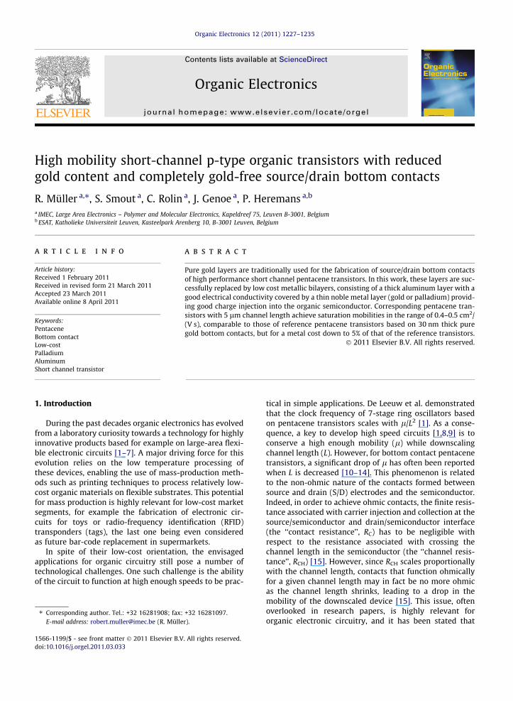
So far, gold has proven to be the most successful mate-rial for the fabrication of source and drain (S/D) electrodesof bottom gate (BG) bottom contact (BC) transistors(Fig. 1a) used as building blocks of high speed organic cir-cuits. This can be attributed to its manifold benefits suchas: (i) high chemical inertness (no spontaneous oxidationin air) allowing easy cleaning after photolithographic pat-terning (for example by solvents, strong chemical oxidizersor ultraviolet–ozone (UV/O3)), (ii) simple deposition byevaporation or sputtering, (iii) good electrical conductivity,and (iv) the ability to fix self-assembled monolayers(SAMs) that improves charge injection into the organicsemiconductor, enabling ohmic contacts, an asset for suc-cessful transistor downscaling. All these properties to-gether lead to well-behaved pentacene transistors basedon gold S/D BC exhibiting low contact resistance and highextrinsic hole saturation mobilities (lsat) of up to 0.5–1 cm2/(V s) even for short channel lengths (L 6 10 lm)[17]. Further on, gold has proven to be the material ofchoice to successfully scale-down transistor dimensions,thus boosting circuit speeds. Current high-speed state-of-the art organic circuits such as full-wave rectifier circuitsoperating at 13.56 MHz [18] and 64-bit and 128-bit plastictransponder chips for RFID-tags [6] are based on pentacenetransistors with gold S/D BCs. On the other hand, the highcost of the gold layer (typical thickness of around 30 nm[8]) precludes commercialization in low-cost applicationssuch as RFID-tags. Indeed, for a 1 cm2 area RFID-tag [6]the cost of such a gold layer (based on the current goldprice of 44 USD per gram) would already reach 25% ofthe target price of 0.01 USD, to which additional costs ofthe antenna, the substrate, the dielectric, the organic semi-conductor, solvents and chemicals, yields below 100%, andthe processing have to be added.
During the past years a huge number of alternative BCmaterials for pentacene transistors have been investigated,such as metals [19–24], metal oxides [22,24], ionic salts[25–27], carbon (including carbon nanotubes and graph-ene [28–35]) and conductive polymers [36–39]. For someof the non metallic materials, pentacene BG BC transistorswith mobilities in the range of 0.1–1 cm2/(V s) could beachieved with large channel lengths [24–26,28,29,32,37,39]. However, this does not imply that such
Fig. 1. (a) Schematic view of a BG BC pentacene transistor (optional surface modiclarity); (b) Optical micrograph of a bottom S/D contacts (W/L = 2500/5 lm/lm
high carrier mobility could be reached for similar transis-tors with short channel lengths, a requirement for highspeed organic circuits. Academic research has proven thatmobilities within the 10�2 cm2/(V s) range can be reachedwith organic semiconductors and metallic or conductivepolymer based BCs of sub-micrometer channel length[36,40–42], where the channels were defined by innova-tive processes such as nanoscratching and self-alignedprinting. Although such developments are highly valuablefor future generations of organic electronic circuits, addi-tional research will likely be required for reaching suffi-cient high yield of operational transistors and low spreadof their electrical parameters required for circuits involv-ing several hundred organic transistors [6], which can cur-rently be obtained with photolithography based patterningof S/D BCs.
In this paper, we propose a different approach towardscost-effective while high performing S/D electrodes. Theseconsist of metallic bilayers: a thick layer of an inexpensivefirst metal, Ti or Al, directly deposited onto the substrate,assuring good adhesion and high electrical conductivity,and a second, thin layer – deposited above the first one –of a noble metal, Au or Pd, providing good charge injectioninto pentacene. Using these metallic bilayer structures, wedemonstrate the feasibility of low cost, short channel(L 6 5 lm) BG BC pentacene transistors, yielding perfor-mances that favorably compare to equivalent referencetransistors based on 30 nm thick Au-only S/D electrodes,and this for metal costs down to 5% of those of the tradi-tional route.
2. Experimental
Transistors were processed on a highly doped Si wafer(200 mm diameter, IMEC production line) with aluminumbackside, acting respectively as the substrate and the gateelectrode. A uniform, about 140 nm thick thermally grownSiO2 provides the gate dielectric; the exact thickness ofwhich is evaluated by ellipsometry. Source and drain elec-trodes made with various metallizations (see below) werepatterned by double layer photoresist (AZ6612 and LOR™1A (MicroChem)) lithography and lift-off. The use of a dou-ble layer resist permits a negative slope that ensures theabsence of spikes after resist lift-off. Subsequently, thesubstrates were thoroughly cleaned by ultrasonication inacetone (10 min.) and isopropylalcohol (10 min), blowndry with nitrogen, and cleaned by a UV/O3 step (15 min).A self-assembled monolayer of pentafluorobenzenethiol(PFBT) was then deposited from a 5 mM solution in ethanol
fication layer on the dielectric and the S/D bottom contacts are omitted for) on SiO2; and (c) Chemical structure of pentacene, PFBT and PETS.
R. Müller et al. / Organic Electronics 12 (2011) 1227–1235 1229
(30 min) onto the Au containing S/D contacts; this step wasomitted for Pd metallizations. Then a silane based self-assembled monolayer was deposited onto the SiO2 dielec-tric by exposure of the substrates to vapors of phenylethyl-trichlorosilane (PETS, 60 �C, reduced pressure) during30 min. Pentacene, purified by gradient sublimation, wasevaporated onto the substrates in an ultrahigh vacuumchamber (10�8 Torr) at 0.25 Å/s, while the substrate waskept at 68 �C. After pentacene evaporation, the sampleswere directly transferred from the vacuum chamber intoa nitrogen filled glovebox ([O2] < 1 ppm, [H2O] < 1 ppm),where transistors were measured using an Agilent 4156Cparameter analyzer. All indicated mobilities were evalu-ated in saturation mode. Transistor structures had nominalchannel width/length (W/L) of 2500 lm/5 lm. Exact chan-nel lengths (typically around 3.7–4.5 lm), measured byoptical microscopy (Olympus AX70) were used for thecomputation of the saturation mobility and are reportedin the corresponding figures. BC substrates were character-ized by scanning electron microscopy (SEM, Philips XL30)and the morphology of the organic polycrystalline film byatomic force microscopy (AFM, Agilent 5100), operated intapping mode.
3. Results and discussion
In order to replace the 30 nm thick (sputtered) Au layerused in our standard process BCs, we investigated alterna-tive BC metallizations consisting of thin (5 nm) Au and Pdlayers formed on a thicker (25 nm) evaporated Al layer.Although preliminary experiments revealed that Ti(25 nm) is also suitable for this lower layer, the entirestudy reported within this paper is performed with Al. In-deed, this metal – in addition to lower cost – has a signif-icant lower electrical resistivity as compared to that of Ti(Table 1) [43].
A simple calculation, based on resistivity values indi-cated in Table 1 and the formula of two resistors connectedin parallel, reveals that the resistance of the BC consistingof 5 nm Au on 25 nm Al, and 5 nm Pd on 25 nm Al, arerespectively only 15% and 35% higher to that of a 30 nmthick pure Au layer. This slight increase in resistivity isfully acceptable for the envisaged circuit applications.
Since Al adheres very well to SiO2 it was also possible toinvestigate a thin evaporated Au layer on top of Al, in addi-tion to the thin sputtered Au layer on Al. As will be shownlater, this processing detail leads to a significant differencein electrical performance of the corresponding pentacenetransistors.
Table 1Electrical resistivity of metals at 20 �C. The value for Cu is given forcomparison.
Metal (Symbol) Electrical resistivity lX cm at 20 �C [43]
Gold (Au) 2.24Palladium (Pd) 10.54Aluminum (Al) 2.6548Titanium (Ti) 42.0Copper (Cu) 1.678
3.1. Characterization of bottom contacts with differentmetallizations schemes
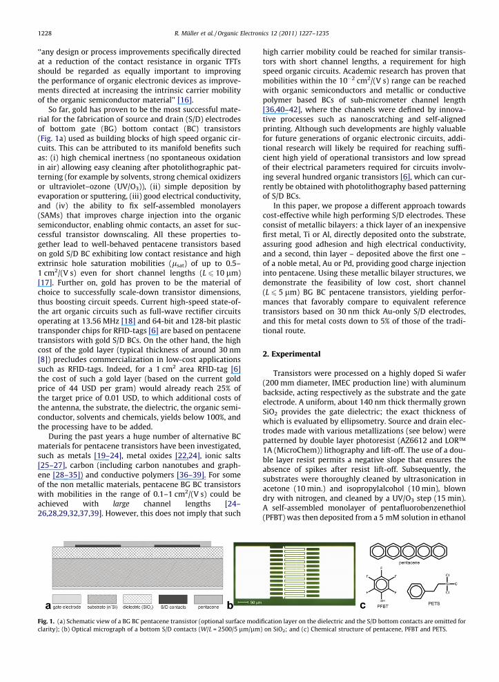
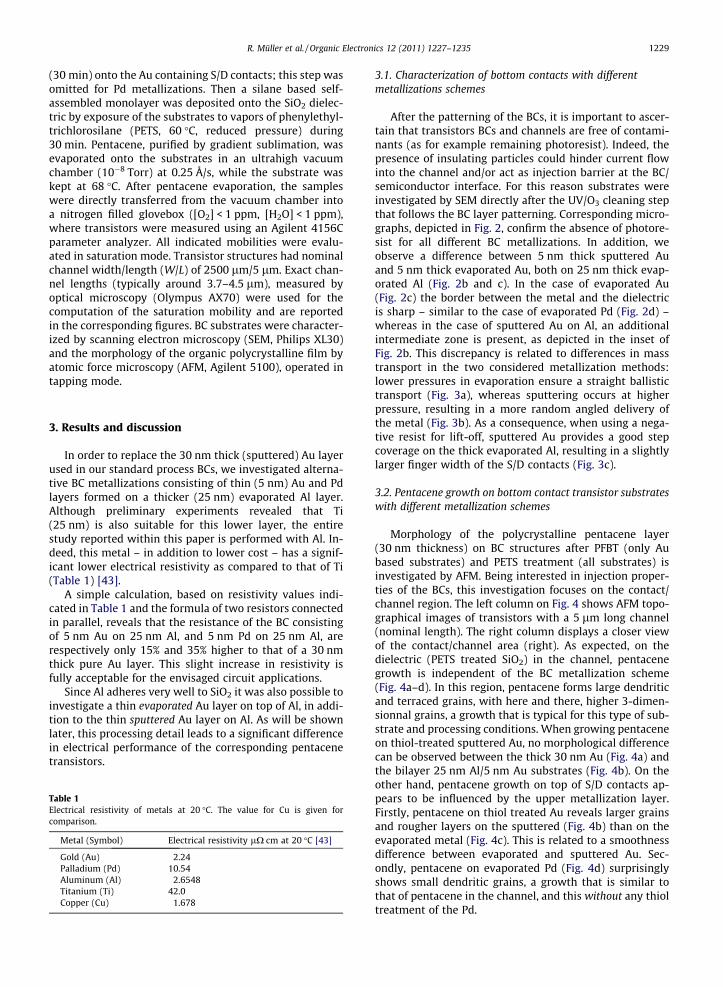
After the patterning of the BCs, it is important to ascer-tain that transistors BCs and channels are free of contami-nants (as for example remaining photoresist). Indeed, thepresence of insulating particles could hinder current flowinto the channel and/or act as injection barrier at the BC/semiconductor interface. For this reason substrates wereinvestigated by SEM directly after the UV/O3 cleaning stepthat follows the BC layer patterning. Corresponding micro-graphs, depicted in Fig. 2, confirm the absence of photore-sist for all different BC metallizations. In addition, weobserve a difference between 5 nm thick sputtered Auand 5 nm thick evaporated Au, both on 25 nm thick evap-orated Al (Fig. 2b and c). In the case of evaporated Au(Fig. 2c) the border between the metal and the dielectricis sharp – similar to the case of evaporated Pd (Fig. 2d) –whereas in the case of sputtered Au on Al, an additionalintermediate zone is present, as depicted in the inset ofFig. 2b. This discrepancy is related to differences in masstransport in the two considered metallization methods:lower pressures in evaporation ensure a straight ballistictransport (Fig. 3a), whereas sputtering occurs at higherpressure, resulting in a more random angled delivery ofthe metal (Fig. 3b). As a consequence, when using a nega-tive resist for lift-off, sputtered Au provides a good stepcoverage on the thick evaporated Al, resulting in a slightlylarger finger width of the S/D contacts (Fig. 3c).
3.2. Pentacene growth on bottom contact transistor substrateswith different metallization schemes
Morphology of the polycrystalline pentacene layer(30 nm thickness) on BC structures after PFBT (only Aubased substrates) and PETS treatment (all substrates) isinvestigated by AFM. Being interested in injection proper-ties of the BCs, this investigation focuses on the contact/channel region. The left column on Fig. 4 shows AFM topo-graphical images of transistors with a 5 lm long channel(nominal length). The right column displays a closer viewof the contact/channel area (right). As expected, on thedielectric (PETS treated SiO2) in the channel, pentacenegrowth is independent of the BC metallization scheme(Fig. 4a–d). In this region, pentacene forms large dendriticand terraced grains, with here and there, higher 3-dimen-sionnal grains, a growth that is typical for this type of sub-strate and processing conditions. When growing pentaceneon thiol-treated sputtered Au, no morphological differencecan be observed between the thick 30 nm Au (Fig. 4a) andthe bilayer 25 nm Al/5 nm Au substrates (Fig. 4b). On theother hand, pentacene growth on top of S/D contacts ap-pears to be influenced by the upper metallization layer.Firstly, pentacene on thiol treated Au reveals larger grainsand rougher layers on the sputtered (Fig. 4b) than on theevaporated metal (Fig. 4c). This is related to a smoothnessdifference between evaporated and sputtered Au. Sec-ondly, pentacene on evaporated Pd (Fig. 4d) surprisinglyshows small dendritic grains, a growth that is similar tothat of pentacene in the channel, and this without any thioltreatment of the Pd.
Fig. 2. Scanning electron micrographs (top view) of BC metallizations on SiO2: (a) 30 nm sputtered Au, (b) 5 nm sputtered Au on 25 nm evaporated Al, (c)5 nm evaporated Au on 25 nm evaporated Al, and (d) 5 nm evaporated Pd on 25 nm evaporated Al.
Fig. 3. Schematic representation of the BC metallization process: (a) evaporated metal (Au), (b) sputtered metal (Au), (c) thin layer of sputtered metal (Au)on top of a thicker layer evaporated metal (Al).
1230 R. Müller et al. / Organic Electronics 12 (2011) 1227–1235
In the closer view of the contact/channel interface (rightcolumn of Fig. 4), it appears that, in all cases, pentacenetwo dimensional grains nucleate along the metal walland subsequently grow inside the channel by step flow.This leaves a pattern of superimposed terraces all stem-
ming from the same nucleation point and propagating in-side the channel. In the case of the thin sputtered Aulayer on Al, the small grained morphology that is typicalof pentacene growth on top of thiol treated Au slightly ex-tends to the right of the thick contact region (Fig. 4b,
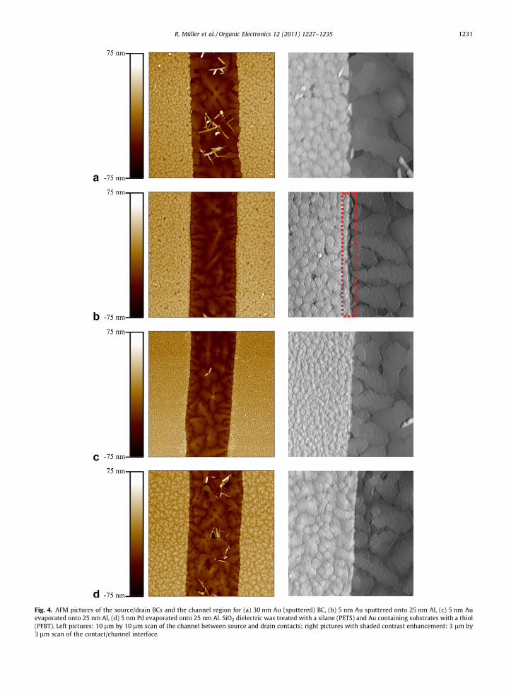
Fig. 4. AFM pictures of the source/drain BCs and the channel region for (a) 30 nm Au (sputtered) BC, (b) 5 nm Au sputtered onto 25 nm Al, (c) 5 nm Auevaporated onto 25 nm Al, (d) 5 nm Pd evaporated onto 25 nm Al. SiO2 dielectric was treated with a silane (PETS) and Au containing substrates with a thiol(PFBT). Left pictures: 10 lm by 10 lm scan of the channel between source and drain contacts; right pictures with shaded contrast enhancement: 3 lm by3 lm scan of the contact/channel interface.
R. Müller et al. / Organic Electronics 12 (2011) 1227–1235 1231
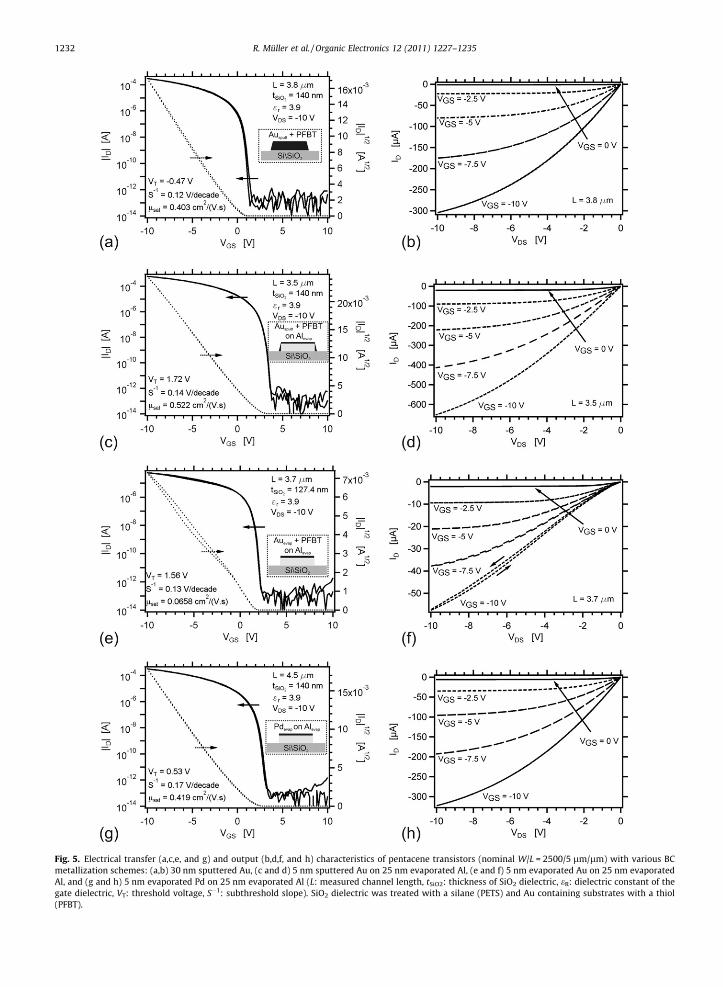
Fig. 5. Electrical transfer (a,c,e, and g) and output (b,d,f, and h) characteristics of pentacene transistors (nominal W/L = 2500/5 lm/lm) with various BCmetallization schemes: (a,b) 30 nm sputtered Au, (c and d) 5 nm sputtered Au on 25 nm evaporated Al, (e and f) 5 nm evaporated Au on 25 nm evaporatedAl, and (g and h) 5 nm evaporated Pd on 25 nm evaporated Al (L: measured channel length, tSiO2: thickness of SiO2 dielectric, eR: dielectric constant of thegate dielectric, VT: threshold voltage, S�1: subthreshold slope). SiO2 dielectric was treated with a silane (PETS) and Au containing substrates with a thiol(PFBT).
1232 R. Müller et al. / Organic Electronics 12 (2011) 1227–1235
R. Müller et al. / Organic Electronics 12 (2011) 1227–1235 1233
dashed rectangle). This confirms the earlier observationthat the thin sputtered Au layer extends beyond the widthof the evaporated Al (inset in Fig. 2b).
Previously reported SEM micrographs published byBock et al. [20] for pentacene growth on 25 nm thick Pdand Au bottom contacts (both on 1 nm thick Ti adhesionlayer and without thiol treatment) showed a film morphol-ogy similar in the channel and on the Pd electrode, but noton the Au electrode. Our results indicate that the metallicbilayer structure is not detrimental for pentacene growth.In all studied cases, homogeneous pentacene films can beobtained.
3.3. Effect of bottom contact metallization on transistorcharacteristics
Electrical performances of the investigated S/D metalli-zation schemes for pentacene BG BC transistors with nom-inal W/L = 2500 lm/5 lm are shown in Fig. 5, with transferand output curves respectively in the left and in the rightcolumn. The reference transistor with 30 nm thick Au BCdisplays well-behaved characteristics. From the transfercurve, a saturation mobility l of 0.4 cm2/(V s) and athreshold voltage VT close to 0 V are extracted (Fig. 5a).The output curve displays a good saturation behavior withno evidence of injection problem at the contacts. Suchcharacteristics are fully representative of a stable and opti-mized pentacene BG BC transistor technology. We observecomparable characteristics for pentacene transistors with5 nm sputtered Au on 25 nm evaporated Al (Fig. 5c andd) and with 5 nm evaporated Pd on 25 nm evaporated Al(Fig. 5g and h). Both metallic bilayer BC architectures deli-ver excellent transistors, with l in the range of 0.4–0.5 cm2/(V s), low VT and no evidence of injection problemsat the contacts. On the other hand, in the case of the 5 nmevaporated Au on 25 evaporated Al BC architecture, the S-shaped output curves in Fig. 5f clearly exhibit signs of non-ohmic contacts [44]. This adversely affects the source/drain current flowing through the device whose l de-creases by almost one order of magnitude (Fig. 5e).Thisunexpected difference between a thin sputtered (Fig. 5cand d) and evaporated (Fig. 5e and f) Au film on Al findsits explanation in the earlier evidences from the SEM andAFM device characterizations that sputtered Au extendsbeyond the width of the evaporated Al film whereas theevaporated Au has the same width as the Al film under-neath. Indeed, experiments reported for BG BC pentacenetransistors with 50 nm thick Au layers on 0.5–10 nm thickTi adhesion layers revealed that good charge injection intothe pentacene could only be achieved for Ti layer thick-nesses below 3 nm, which is about the thickness of theaccumulation layer in a pentacene channel [12]. Therequirement to have a direct contact between the noblemetal and the pentacene in the transistor channel regionexplains why the BC metallization with evaporated Au onAl led to poor charge injection (Fig. 5e and f) whereas injec-tion from the sides of the sputtered Au on Al led to excel-lent transistor properties (Fig. 5c and d).
Considering this advantage of sputtering over evapora-tion for the thin Au layer, it is surprising that we obtainsuch good transistors for the 5 nm evaporated Pd on
25 nm Al BC architecture (Fig. 5g and h) who favorablycompare to those reported in the pioneering work by Klauket al. on pentacene transistors based on ion-beam sput-tered Pd BC [10]. Moreover the absence of any specific con-tact treatment besides the UV/O3 exposure constitutes anadvantage of Pd over the for Au obligatory thiol treatment,leading to potentially air sensitive Au-thiolates [45]. Thereason for not encountering similar injection problemswith the thin evaporated Pd as with the thin evaporatedAu is not clear. It could find its origin in the improved con-tinuity of the pentacene film formed on top of the Pd con-tact and on top of the dielectric in the channel, as hinted bythe similar dendritic morphologies in Fig. 4d.
3.4. Metal cost reduction for S/D bottom contacts
Since noble metals like gold and palladium are signifi-cantly more expensive than aluminum, simple calculations– neglecting the cost of the aluminum layer – have beenmade in order to estimate the material cost reduction byusing a 5 nm thin Au or Pd layer as metallization for BC in-stead of a 30 nm thick pure Au layer. In this way, metalli-zation cost of the thin Au layer was only 1/6th of thestandard Au metallization, and this with similar perfor-mance of the short-channel pentacene transistors(Fig. 5a–d).
The relative metallization cost of a 5 nm thick Pd layerwith respect to 30 nm thick Au layer was calculated usingthe following formula, in which CM, dM, AM, qM and PM
respectively represent the metallization cost, the layerthickness, the metallization area, the density, and theprize/weight of the metal M:
CM ¼ dM � AM � qM � PM
From this formula, the ratio of CAu/CPd was computed asfollows:
CAu
CPd¼ dAu
dPd� AAu
APd� qAu
qPd� PAu
PPd
Knowing (i) that the metallization areas are identical forAu and Pd, (ii) dAu = 30 nm and dPd = 5 nm, (iii) qAu = 19.30and qPd = 12.0 g/cm3 at 20 �C [46] and (iii) the current ratioof the gold prize with respect to the palladium prize PAu/PPd � 2.1, the metallization cost ratio is CAu/CPd � 19.8.
This indicates that the material cost of a 5 nm thin Pdlayer (on 25 nm thick Al) is only about 5% of the cost ofthe traditional metallization consisting of 30 nm Au.
4. Conclusions
The issue addressed in this paper can be wrapped up inthe three following facts: (i) organic circuits require highmobility short channel pentacene transistors to reach suf-ficient speeds, (ii) up to now, such high mobilities in shortchannel devices could only be achieved with Au S/D con-tacts, (iii) in mass production, the gold cost amounts fora significant fraction of the final device price. In this work,we prove the concept of using metallic bilayers (5 nm thinsputtered Au or evaporated Pd on 25 nm thick evaporatedAl) as replacement of traditional plain Au (30 nm thick) S/D
1234 R. Müller et al. / Organic Electronics 12 (2011) 1227–1235
contacts in short channel (L 6 5 lm) pentacene BG BC tran-sistors. Using this new BC architecture, transistors achievesimilar saturation hole mobilities to those of referencetransistors with pure Au contacts, and this with at metalcosts of respectively 17% and 5% of the reference transistor.With its equivalent performance at a significantly lowercost, the bilayer approach presented here represents theonly credible alternative to plain Au electrodes and canbe considered as significant step towards the commercial-ization of low-cost high quality organic electronic circuits.The achievement of good electrical performance withbilayers consisting of evaporated metals is furthermorepromising for future cost reductions since the metal bi-layer profile can be expected to be similar to the one ob-tained by etching processes, which typically gives higheryields than lift-off processes and are therefore used inindustrial processes of the display industry.
Acknowledgments
Erwin Vandenplas (IMEC) is acknowledged for metaldeposition on the substrates. This work was performed ina collaboration between IMEC and TNO in the frame ofthe HOLST Centre. The authors acknowledge financial sup-port of EC-funded project Polaric (FP7-247978).
References
[1] D.M. de Leeuw, G.H. Gelinck, T.C.T. Geuns, E. van Veenendaal, E.Cantatore, B.H. Huisman, Polymeric integrated circuits: fabricationand first characterisation, IEDM Tech. Digest. (2002) 293–296.
[2] P.F. Baude, D.A. Ender, M.A. Haase, T.W. Kelley, D.V. Muyres, S.D.Theiss, Pentacene-based radio-frequency identification circuitry,Appl. Phys. Lett. 82 (2003) 3964–3966.
[3] G. Gelinck, P. Heremans, K. Nomoto, T.D. Anthopoulos, Organictransistors in optical displays and microelectronic applications, Adv.Mat. 22 (2010) 3778–3798.
[4] T. Sekitani, U. Zschieschang, H. Klauk, T. Someya, Flexible organictransistors and circuits with extreme bending stability, Nat. Mat. 9(2010) 1015–1022.
[5] K. Myny, S. Steudel, S. Smout, P. Vicca, F. Furthner, B. van der Putten,A.K. Tripathi, G.H. Gelinck, J. Genoe, W. Dehaene, P. Heremans,Organic RFID transponder chip with data rate compatible withelectronic product coding, Org. Electron. 11 (2010) 1176–1179.
[6] K. Myny, S. Steudel, P. Vicca, M.J. Beenhakkers, N.A.J.M. van Aerle,G.H. Gelinck, J. Genoe, W. Dehaene, P. Heremans, Plastic circuits andtags for 13.56 MHz radio-frequency communication, Solid-StateElectron. 53 (2009) 1220–1226.
[7] T.W. Kelley, P.F. Baude, C. Gerlach, D.E. Ender, D. Muryres, M.A.Haase, D.E. Vogel, S.D. Theiss, Recent progress in organic electronics:materials, devices, and processes, Chem. Mater. 16 (2004) 4413–4422.
[8] H. Klauk, M. Halik, U. Zschieschang, F. Eder, G. Schmid, C. Dehm,Pentacene organic transistors and ring oscillators on glass and onflexible polymeric substrates 82 (2003) 4175–4177.
[9] B.C. Shekar, J. Lee, S.-W. Rhee, Organic thin film transistors: materialsprocesses and devices, Korean J. Chem. Eng. 21 (2004) 267–285.
[10] H. Klauk, G. Schmid, W. Radlik, W. Weber, L. Zhou, C.D. Sheraw, J.A.Nichols, T.N. Jackson, Contact resistance in organic thin filmtransistors, Solid-State Electron. 47 (2003) 297–301.
[11] J. Zaumseil, K.W. Baldwin, J.A. Rogers, J. Appl. Phys. 93 (2003) 6117–6124.
[12] N. Yoneya, M. Noda, H. Hirai, K. Nomoto, M. Wada, J. Kasahara,Reduction of contact resistance in pentacene thin-film transistors bydirect carrier injection into a-few-molecular-layer channel, Appl.Phys. Lett. 85 (2004) 4663–4665.
[13] D.J. Gundlach, L. Zhou, J.A. Nichols, T.N. Jackson, P.V. Necliudov, M.S.Shur, An experimental study of contact effects in organic thin filmtransistors, J. Appl. Phys. 100 (2006) 024509.
[14] H. Kim, R.C.Y. Auyeung, S.H. Lee, A.L. Huston, A. Piqué, Laser forwardtransfer of silver electrodes for organic thin-film transistors, Appl.Phys. A 69 (2009) 441–445.
[15] M.J. Panzer, C.D. Frisbie, Contact effects in organic field-effecttransistors, in: Z. Bao, J. Locklin (Eds.), Organic field-effecttransistors Vol. 128, Optical Science and Engineering Series, CRCPress, 2007, pp. 139–157.
[16] J.-A. Chu, J.-J. Zeng, K.-C. Wu, Y.-J. Lin, Pentacene ohmic contact onthe transparent conductive oxide films, Thin Solid Films 519 (2010)868–871.
[17] S. De Vusser, S. Steudel, K. Myny, J. Genoe, P. Heremans, Integratedshadow mask method for patterning small molecule organicsemiconductors, Appl. Phys. Lett. 88 (2006) 103501.
[18] R. Rotzoll, S. Mohapatra, V. Olariu, R. Wenz, M. Grigas, K. Dimmler, O.Shchekin, A. Dodabalapur, Radio frequency rectifiers based onorganic thin-film transistors, Appl. Phys. Lett. 88 (2006) 123502.
[19] C.-L. Fan, T.-H. Yang, C.-Y. Chiang, Performance degradation ofpentacene-based organic thin-film transistors under positive drainbias stress in the atmosphere, IEEE Electr. Dev. Lett. 31 (2010) 887–889.
[20] C. Bock, D.V. Pham, U. Kunze, D. Käfer, G. Witte, Ch. Wöll, Influenceof contact metals on the performance and morphology of pentacenebottom-contact field-effect transistors, Phys. E 40 (2008) 2107–2109.
[21] D.J. Gundlach, L.L. Jia, T.N. Jackson, Pentacene TFT with improvedlinear region characteristics using chemically modified source anddrain electrodes, IEEE Electr. Dev. Lett. 22 (2001) 571–573.
[22] S.-W. Rhee, D.-J. Yun, Metal-semiconductor contact in organic thinfilm transistors, J. Mat. Chem. 18 (2008) 5437–5444.
[23] H. Kim, R.C.Y. Auyeung, S.H. Lee, A.L. Huston, A. Piqué, Laser forwardtransfer of silver electrodes for organic thin-film transistors, Appl.Phys. A 96 (2009) 441–445.
[24] D.-J. Yun, S. Lee, K. Yong, S.-W. Rhee, In situ ultravioletphotoemission spectroscopy measurement of the pentacene-RuO2/Ti contact energy structure, Appl. Phys. Lett. 97 (2010) 073303.
[25] C.-a. Di, G. Yu, Y. Liu, X. Xu, D. Wei, Y. Song, Y. Sun, Y. Wang, D. Zhu, J.Liu, X. Liu, D. Wu, High-performance low-cost organic field-effecttransistors with chemically modified bottom electrodes, J. Am.Chem. Soc. 128 (2006) 16418–16419.
[26] K. Shibata, H. Wada, K. Ishikawa, H. Takezoe, T. Mori,(Tetrathiafulvalene)(tetracyanoquinodimethane) as a low-contact-resistance electrode for organic transistors, Appl. Phys. Lett. 90(2007) 193509.
[27] Y. Yu, M. Kanno, H. Wada, Y. Bando, M. Ashizawa, A. Tanioka, T. Mori,Enhanced performance of bottom-contact organic field-effecttransistors with M(DMDCNQI)2 buffer layers, Physica B 405 (2010)S378–S380.
[28] H. Wada, T. Mori, Solution-processed carbon electrodes for organicfield-effect transistors, Appl. Phys. Lett. 93 (2008) 213303.
[29] H. Wada, T. Mori, High-resolution transparent carbon electrodes fororganic field-effect transistors patterned by laser sintering, Appl.Phys. Lett. 95 (2009) 253307.
[30] J.-I. Inoue, H. Wada, T. Mori, Self contact organic transistors, Jap. J.Appl. Phys. 49 (2010) 071605.
[31] C.-a. Di, D. Wei, G. Yu, Y. Liu, Y. Guo, D. Zhu, Patterned graphene assource/drain electrodes for bottom-contact organic field-effecttransistors, Adv. Mater. 20 (2008) 3289–3293.
[32] C.-H. Chang, C.-H. Chien, J.-Y. Yang, Pentacene-based thin-filmtransistors with multiwalled carbon nanotube source and drainelectrodes, Appl. Phys. Lett. 91 (2007) 083502.
[33] Y. Chen, Y. Xu, K. Zhao, X. Wan, J. Deng, W. Yan, Towards flexible all-carbon electronics: flexible organic field- effect transistors andinverter circuits using solution-processed all-graphene source/drain/gate electrodes, Nano Res. 3 (2010) 714–721.
[34] H.A. Becerril, R.M. Stoltenberg, M.L. Tang, M.E. Roberts, Z. Liu, Y.Chen, D.H. Kim, B.-L. Lee, S. Lee, Z. Bao, Fabrication and evaluation ofsolution-processed reduced graphene oxide electrodes for p- and n-channel bottom-contact organic thin-film transistors, ACS Nano 4(2010) 6343–6352.
[35] S. Lee, G. Jo, S.-J. Kang, G. Wang, M. Choe, W. Park, D.-Y. Kim, Y.H.Kahng, T. Lee, Enhanced charge injection in pentacene field-effecttransistors with graphene electrodes, Adv. Mater. 23 (2011) 100–105.
[36] L. Li, M. Hirtz, W. Wang, C. Du, H. Fuchs, L. Chi, Patterning of polymerelectrodes by nanoscratching, Adv. Mater. 22 (2010) 1374–1378.
[37] M.A. Ali, H.H. Kim, K.H. Jeong, H.S. Soh, H.S. Nam, J.G. Lee, E.G. Lee,Application of poly(3 tosylate-doped 4ethylenedioxythiophene)(PEDOT) films into bottom contact pentacene organic thin filmtransistors (OTFTs), Thin Solid Films 518 (2010) 6315–6319.
R. Müller et al. / Organic Electronics 12 (2011) 1227–1235 1235
[38] P. Cosseddu, A. Bonfiglio, Soft lithography fabrication of all-organicbottom-contact and top-contact field effect transistors, Appl. Phys.Lett. 88 (2006) 023506.
[39] S.L. Hellstrom, R.Z. Jin, R.M. Stoltenberg, Z. Bao, Driving high-performance n- and p-type organic transistors with carbonnanotube/conjugated polymer composite electrodes patterneddirectly from solution, Adv. Mater. 22 (2010) 4204–4208.
[40] J.Z. Wang, Z.H. Zheng, H.W. Li, W.T.S. Huck, H. Sirringhaus, Polymerfield effect transistors fabricated by dewetting, Synth. Met. 146(2004) 287–290.
[41] M. Leufgen, U. Bass, T. Muck, T. Borzenko, G. Schmidt, J. Geurts, V.Wagner, L.W. Molenkamp, Optimized sub-micron organic thin-filmtransistors: the influence of contacts and oxide thickness, Synth.Met. 146 (2004) 341–345.
[42] C.W. Sele, T. von Werne, R.H. Friend, H. Sirringhaus, Lithography-freeself-aligned inkjet printing with sub-hundred-nanometer resolution,Adv. Mater. 17 (2005) 997–1001.
[43] CRC Handbook of Chemistry and Physics, 64th edition, 1983-1984,CRC Press, Boca Raton (Fl), p. F–125.
[44] G. Horowitz, Interfaces in organic field-effect transistors, Adv.Polym. Sci. 223 (2010) 113–153.
[45] M.-T. Lee, C.-C. Hsueh, M.S. Freund, G.S. Ferguson, Air oxidation ofself-assembled monolayers on polycrystalline gold: the role of thegold substrate, Langmuir 14 (1998) 6419–6423.
[46] CRC Handbook of Chemistry and Physics, 64th edition, 1983-1984,CRC Press, Boca Raton (Fl), pp. B-94 and B-118.