BRAIN DRAIN 1 Economic Impact of Brain Drain in Developed ...
Upload
khangminh22Category
view
2download
0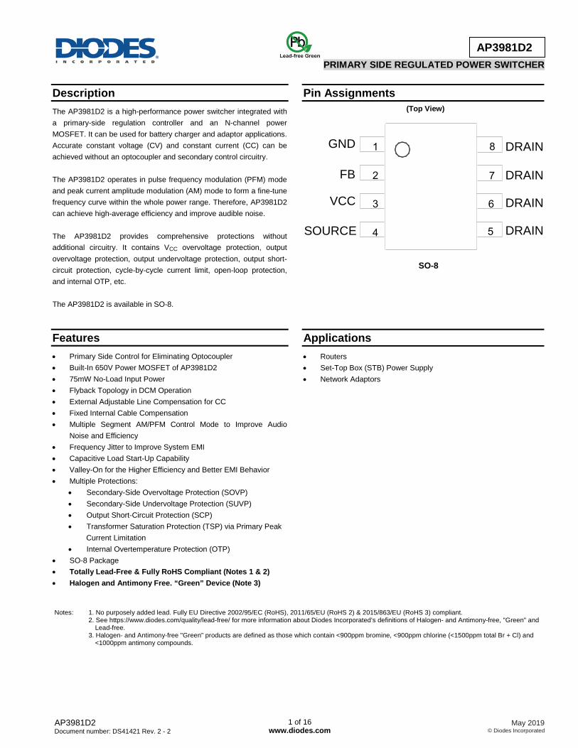
AP3981D2 PRIMARY SIDE REGULATED POWER SWITCHER
Description The AP3981D2 is a high-performance power switcher integrated with a primary-side regulation controller and an N-channel power MOSFET. It can be used for battery charger and adaptor applications. Accurate constant voltage (CV) and constant current (CC) can be achieved without an optocoupler and secondary control circuitry. The AP3981D2 operates in pulse frequency modulation (PFM) mode and peak current amplitude modulation (AM) mode to form a fine-tune frequency curve within the whole power range. Therefore, AP3981D2 can achieve high-average efficiency and improve audible noise. The AP3981D2 provides comprehensive protections without additional circuitry. It contains VCC overvoltage protection, output overvoltage protection, output undervoltage protection, output short-circuit protection, cycle-by-cycle current limit, open-loop protection, and internal OTP, etc. The AP3981D2 is available in SO-8.
Features • Primary Side Control for Eliminating Optocoupler • Built-In 650V Power MOSFET of AP3981D2 • 75mW No-Load Input Power • Flyback Topology in DCM Operation • External Adjustable Line Compensation for CC • Fixed Internal Cable Compensation • Multiple Segment AM/PFM Control Mode to Improve Audio
Noise and Efficiency • Frequency Jitter to Improve System EMI • Capacitive Load Start-Up Capability • Valley-On for the Higher Efficiency and Better EMI Behavior • Multiple Protections:
• Secondary-Side Overvoltage Protection (SOVP) • Secondary-Side Undervoltage Protection (SUVP) • Output Short-Circuit Protection (SCP) • Transformer Saturation Protection (TSP) via Primary Peak
Current Limitation • Internal Overtemperature Protection (OTP)
• SO-8 Package • Totally Lead-Free & Fully RoHS Compliant (Notes 1 & 2) • Halogen and Antimony Free. “Green” Device (Note 3)
Pin Assignments
(Top View)
SO-8
Applications • Routers • Set-Top Box (STB) Power Supply • Network Adaptors
Notes: 1. No purposely added lead. Fully EU Directive 2002/95/EC (RoHS), 2011/65/EU (RoHS 2) & 2015/863/EU (RoHS 3) compliant. 2. See https://www.diodes.com/quality/lead-free/ for more information about Diodes Incorporated’s definitions of Halogen- and Antimony-free, "Green" and
Lead-free. 3. Halogen- and Antimony-free "Green” products are defined as those which contain <900ppm bromine, <900ppm chlorine (<1500ppm total Br + Cl) and
<1000ppm antimony compounds.
1
2
3
4
8
6
5
7 FB
VCC
SOURCE
GND
DRAIN
DRAIN
DRAIN
DRAIN
AP3981D2 Document number: DS41421 Rev. 2 - 2
1 of 16 www.diodes.com
May 2019 © Diodes Incorporated

AP3981D2
Typical Applications Circuit
AC
R1
C13
T 1
D3
F1
R17
C3
C12
CY1
GND
DRAIN
SOURCE
VCC
AP3981D2
U1
FB
VOUT
GND
C2
L1
5,6,7,8
4
1
R5
R6
2
R18
R2D1
C1
DB1
B1
3
D3
R13R16R15
C10R7 R9
C14
Pin Descriptions
Pin Number Pin Name Function
1 GND IC ground
2 FB Connect to the auxiliary winding through a divider network. Used as a multi-function pin to realize output voltage sample for CV control, tons detection for CC control, line voltage sense for line compensation, and FB-negative-protection detection.
3 VCC IC power supply
4 SOURCE SOURCE terminal of the integrated MOSFET
5, 6,7,8 DRAIN DRAIN terminal of the integrated MOSFET
AP3981D2 Document number: DS41421 Rev. 2 - 2
2 of 16 www.diodes.com
May 2019 © Diodes Incorporated

AP3981D2
Controller Functional Block Diagram
Regulator&
Bias
PFM
t ONS
UVLO
CV_CTRL
PFMValley
ON
R Q
S
R Q
S
FB
VCC
GND
Constant VoltageControl
Constant CurrentControl
tONS
Detector
0.1V
3
1
2
VCS_REF
COMP
EA
Peak CurrentControl & LEB
tONS
Pro
CC_CTRL
ShutdownLineCompensation
DRAIN5, 6, 7, 8
Low PassVCPC
VREF
DriverVLINE
VCC OVPFB OVP/SUVP/SCP
RFB Short/Open ProtectionRcs Short/Open Protection
Transformer Saturation Protection
VCC
VCS
Square RootFunction
CableCompenstaion
VCPC
VCPC4 SOURCE
SOURCE
VCS_REF
AP3981D2 Document number: DS41421 Rev. 2 - 2
3 of 16 www.diodes.com
May 2019 © Diodes Incorporated

AP3981D2
Absolute Maximum Ratings (Note 4)
Symbol Parameter Rating Unit
VCC Supply Voltage -0.3 to 35 V
VSOURCE SOURCE Input Voltage -0.3 to 8 V
VFB FB Input Voltage -0.3 to 8 V
VDS Drain-Source Voltage (TJ=+25°C) 650 V
TJ Operating Junction Temperature -40 to +150 °C
TSTG Storage Temperature -65 to +150 °C
TLEAD Lead Temperature (Soldering, 10 sec) +300 °C
ϴJC Thermal Resistance (Junction to Case) (Note 5) 3 °C/W
ϴJA Thermal Resistance (Junction to Ambient) (Note 5) 65 °C/W
— ESD (Human Body Model) 2000 V
— ESD (Charged Device Model) 1000 V
Notes: 4. Stresses greater than those listed under Absolute Maximum Ratings may cause permanent damage to the device. These are stress ratings only, and functional operation of the device at these or any other conditions beyond those indicated under Recommended Operating Conditions is not implied. Exposure to Absolute Maximum Ratings for extended periods may affect device reliability.
5. Test condition: Device mounted on FR-4 substrate PC board, 2oz copper, with 1in2 cooling area. Recommended Operating Conditions
Symbol Parameter Min Max Unit
VCC Supply Voltage 10 28 V
TA Ambient Temperature -40 +85 °C
AP3981D2 Document number: DS41421 Rev. 2 - 2
4 of 16 www.diodes.com
May 2019 © Diodes Incorporated

AP3981D2
Electrical Characteristics (@TA =+25°C, VCC = 15V, unless otherwise specified.)
Symbol Parameter Condition Min Typ. Max Unit
STARTUP AND UVLO SECTION
VTH_ST Startup Threshold — 14.5 16 17.5 V
VOPR(MIN) Minimum Operating Voltage — 6.1 6.8 7.5 V
STANDBY CURRENT SECTION
IST Startup Current VCC=VTH_ST-1V before Startup — 1 3 µA
ICC_OPR Minimum Operating Current Static Current 450 550 650 µA
CURRENT SENSE SECTION
VCS_H Peak Current Sense Threshold Voltage
40% to 100% CC Load 560 630 700 mV
VCS_L No Load to 2% CC Load 160 180 200 mV
RLINE Built-In Line Compensation Resistor — 45 55 65 Ω
tLEB Leading Edge Blanking — 370 470 570 ns
CONSTANT VOLTAGE SECTION
VFB Feedback Threshold Voltage Closed Loop Test of VOUT 2.35 2.4 2.45 V
RatioSAMPLE_L Sample Ratio No Load to 2% CC Load 45 50 55 %
RatioSAMPLE_H Sample Ratio 40% to 100% CC Load 75 80 85 %
CONSTANT CURRENT SECTION
tONS/tSW Below SUVP Tested @ VFB=1V — 0.75 — —
Above SUVP Tested @ VFB=2V — 0.5 — —
FREQUENCY JITTER
ΔVCS/VCS VCS Modulation 10% Load to Full Load 1.5 2 2.5 %
Cable Compensation
VCABLE/VOUT Fixed Cable Compensation Ratio — — 4 — %
VALLEY-ON SECTION
tVAL-ON Valid Off Time of Valley-on From the End of tONS 26 32 38 µs
DYNAMIC SECTION
tOFF(MAX) Maximum Off Time — 1.8 2 2.2 ms
PROTECTION FUNCTION SECTION
VFB(SOVP) Overvoltage Protection at FB Pin — 3.3 3.6 3.9 V
VFB(SUVP) Undervoltage Protection at FB Pin — 1.22 1.35 1.48 V
tDELAY(SUVP) Delay Time of SUVP — 116 128 140 ms
VFB(SCP) Output Short Protection at FB Pin — 680 750 820 mV
tDELAY(SCP) Delay Time of SCP — 58 64 70 ms
VCC(OVP) Overvoltage Protection at VCC Pin — 29.5 32 34.5 V
tONP(MAX) Maximum Turn-on Time — 12 16 20 µs
VCS(MIN) Minimum Peak Current Sense Voltage at tONP=4µs — 120 150 180 mV
VCS(MAX) Maximum CS Voltage — 720 800 880 mV
AP3981D2 Document number: DS41421 Rev. 2 - 2
5 of 16 www.diodes.com
May 2019 © Diodes Incorporated
AP3981D2
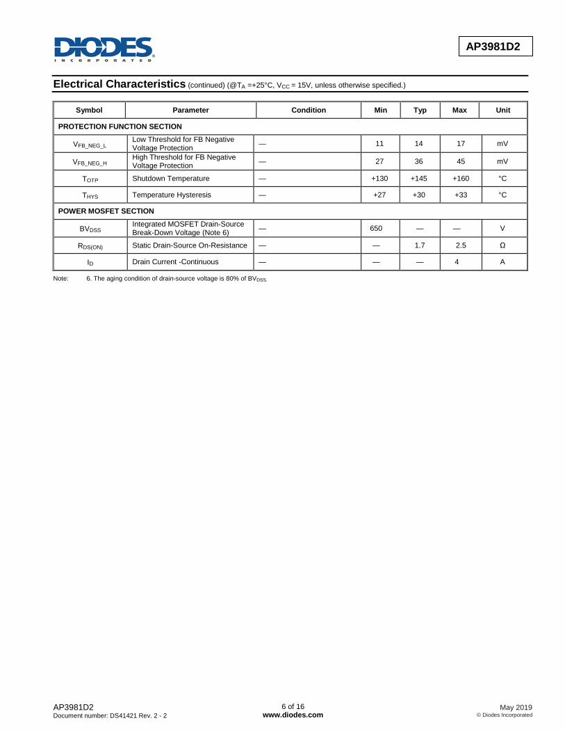
Electrical Characteristics (continued) (@TA =+25°C, VCC = 15V, unless otherwise specified.)
Symbol Parameter Condition Min Typ Max Unit
PROTECTION FUNCTION SECTION
VFB_NEG_L Low Threshold for FB Negative Voltage Protection — 11 14 17 mV
VFB_NEG_H High Threshold for FB Negative Voltage Protection — 27 36 45 mV
TOTP Shutdown Temperature — +130 +145 +160 °C
THYS Temperature Hysteresis — +27 +30 +33 °C
POWER MOSFET SECTION
BVDSS Integrated MOSFET Drain-Source Break-Down Voltage (Note 6) — 650 — — V
RDS(ON) Static Drain-Source On-Resistance — — 1.7 2.5 Ω
ID Drain Current -Continuous — — — 4 A
Note: 6. The aging condition of drain-source voltage is 80% of BVDSS.
AP3981D2 Document number: DS41421 Rev. 2 - 2
6 of 16 www.diodes.com
May 2019 © Diodes Incorporated

AP3981D2
Performance Characteristics
Start-Up Voltage vs. Ambient Temperature
-40 -20 0 20 40 60 80 100 120 14015.0
15.5
16.0
16.5
17.0
17.5
18.0
Ambient Temperature (oC)
Star
t-up
Volta
ge (V
)
Start-Up Current vs. Ambient Temperature
-40 -20 0 20 40 60 80 100 120 1400
1
2
3
4
5
Star
t-up
Curre
nt (µ
A)
Ambient Temperature (oC)
Minimal Operating Voltage vs. Ambient Temperature
-40 -20 0 20 40 60 80 100 120 1403
4
5
6
7
8
Ambient Temperature (oC)
Min
imun
Ope
ratin
g Vo
ltage
(V)
Operating Current vs. Ambient Temperature
-40 -20 0 20 40 60 80 100 120 140300
350
400
450
500
550
600
650
700
Ambient Temperature (oC)
Ope
ratin
g Cu
rrent
(µA)
VCS_H vs. Ambient Temperature
-40 -20 0 20 40 60 80 100 120 140600
620
640
660
680
700
Ambient Temperature (oC)
VCS_
H (m
V)
tONS/tSW Above SUVP vs. Ambient Temperature
-40 -20 0 20 40 60 80 100 120 1400.2
0.3
0.4
0.5
0.6
0.7
0.8
Ambient Temperature (oC)
tONS
/tSW
AP3981D2 Document number: DS41421 Rev. 2 - 2
7 of 16 www.diodes.com
May 2019 © Diodes Incorporated

AP3981D2
Performance Characteristics (continued)
Feedback Voltage vs. Ambient Temperature
-40 -20 0 20 40 60 80 100 120 1402.20
2.25
2.30
2.35
2.40
2.45
2.50
Ambient Temperature (oC)
Feed
back
Vol
tage
(V)
VCC OVP Voltage vs. Ambient Temperature
-40 -20 0 20 40 60 80 100 120 14030
31
32
33
34
35
Ambient Temperature (oC)
Vcc
OVP
vol
tage
(V)
Line Compensation Resistance vs. Ambient Temperature
-40 -20 0 20 40 60 80 100 120 1400
20
40
60
80
100
Ambient Temperature (oC)
Line
Com
pens
atio
n Re
sista
nce
(Ω)
Maximum Off Time vs. Ambient Temperature
-40 -20 0 20 40 60 80 100 120 1401.0
1.5
2.0
2.5
3.0
Ambient Temperature (oC)
Max
imum
Off
Tim
e (m
s)
Low Threshold Voltage for FB_Negative Protection vs.
Ambient Temperature
-40 -20 0 20 40 60 80 100 120 1400
5
10
15
20
25
30
Ambient Temperature (oC)
Low
Thre
shol
d Vo
ltage
for F
B_Ne
g Pr
otec
tion
(mV)
Feedback Voltage of SUVP vs. Ambient Temperature
-40 -20 0 20 40 60 80 100 120 1401.2
1.3
1.4
1.5
1.6
1.7
1.8
Ambient Temperature (oC)
VFB o
f SUV
P (V
)
AP3981D2 Document number: DS41421 Rev. 2 - 2
8 of 16 www.diodes.com
May 2019 © Diodes Incorporated

AP3981D2
Operation Principle Description 1. The Conventional PSR Operating Waveforms
Figure 1: The Operation Waveform of Flyback PSR System
Figure 1 shows the typical waveforms which demonstrate the basic operating principle of AP3981D2 application. The parameters are defined as:
IP — The primary side current IS — The secondary side current IPK — Peak value of primary side current IPKS — Peak value of secondary side current VSEC — The transient voltage at secondary winding VO — The output voltage VAUX — The transient voltage at auxiliary winding VA — The stable voltage at auxiliary winding when rectification diode is in conducting status, which equals the sum of voltage VCC and the forward voltage drop of auxiliary diode tSW — The period of switching frequency tONP — The conduction time when primary side switch is “ON” tONS — The conduction time when secondary side diode is “ON” tOFF — The dead time when neither primary side switch nor secondary side diode is “ON” tOFFS — The time when secondary side diode is “OFF” For primary-side regulation, the primary current ip(t) is sensed by a current sense resistor RCS connected to PIN 4.The current rises up linearly at a rate of:
(1)
MLt
dttdip )(V)( IN=
t ONP t ONS
I PK
I PKS
V O
I P
I S t OFFS
t OFF
V SEC
V A V AUX
t SW
AP3981D2 Document number: DS41421 Rev. 2 - 2
9 of 16 www.diodes.com
May 2019 © Diodes Incorporated

AP3981D2
Operation Principle Description (continued) As shown in Figure 1, when the current ip(t) rises up to IPK, the primary MOSFET turns off. The constant peak current is given by:
(2)
CS
CSPK R
VI =
Therefore, the energy stored in the magnetizing inductance LM each cycle is:
(3)
2
21
PKM ILEg ⋅×=
So the power transferring from the input to the output is given by:
(4)
SWPKM fILP ×××= 2
21
Where the fSW is the switching frequency. When the peak current IPK is constant, the output power depends on the switching frequency fSW. 2. Constant Voltage Operation The output voltage is proportional to the auxiliary winding voltage during tONS period indicated by Equation 5, this auxiliary winding voltage is divided by resistors RFB1 and RFB2 (refer to Figure 5) before inputting to the FB PIN. As shown in Figure 2, AP3981D2 detects the FB voltage at the end of tSAMPLE during tONS period, the detected voltage that reflects the output voltage is regulated to VFB of 2.4V with the help of the constant voltage control block in AP3981D2. For system design, adjust the ratio of RFB1 and RFB2 can get the target output voltage value.
(5)
( )VdVoN
NV
S
AUXAUX +×=
0V
tONS
tSAMPLE
tSW
Figure 2: Auxiliary Voltage Waveform 3. Constant Current Control In AP3981D2, Equation 6 shows the related parameters that determine the output current. To get a constant output current, the VCS and tONS/tSW is fixed in AP3981D2 during CC mode. Meanwhile, a reliable control logic is integrated within AP3981D2 to ensure the system swift smoothly between CC mode and CV mode.
(6)
4. Multiple Segment Peak Current In the original PFM PSR system, the switching frequency decreases with the decreasing output current, which will encounter audible noise issue when switching frequency decreases below 20kHz.
SW
ONS
SW
ONS
tt
RcsVcs
NsNp
ttIpk
NsNpIout ***
21***
21
==
AP3981D2 Document number: DS41421 Rev. 2 - 2
10 of 16 www.diodes.com
May 2019 © Diodes Incorporated
AP3981D2
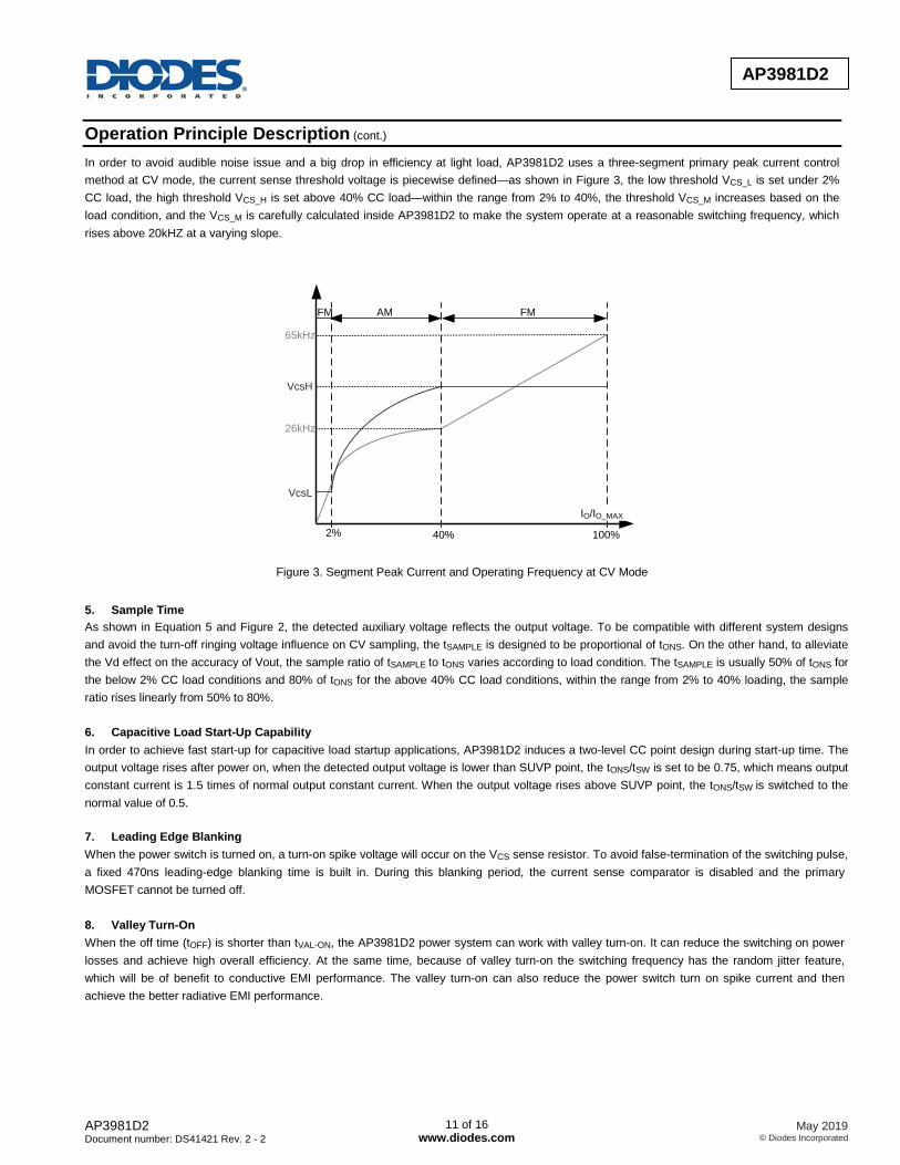
Operation Principle Description (cont.) In order to avoid audible noise issue and a big drop in efficiency at light load, AP3981D2 uses a three-segment primary peak current control method at CV mode, the current sense threshold voltage is piecewise defined—as shown in Figure 3, the low threshold VCS_L is set under 2% CC load, the high threshold VCS_H is set above 40% CC load—within the range from 2% to 40%, the threshold VCS_M increases based on the load condition, and the VCS_M is carefully calculated inside AP3981D2 to make the system operate at a reasonable switching frequency, which rises above 20kHZ at a varying slope.
VcsH
VcsL
AM FMFM
65kHz
26kHz
IO/IO_MAX
100%40%2%
Figure 3. Segment Peak Current and Operating Frequency at CV Mode
5. Sample Time As shown in Equation 5 and Figure 2, the detected auxiliary voltage reflects the output voltage. To be compatible with different system designs and avoid the turn-off ringing voltage influence on CV sampling, the tSAMPLE is designed to be proportional of tONS. On the other hand, to alleviate the Vd effect on the accuracy of Vout, the sample ratio of tSAMPLE to tONS varies according to load condition. The tSAMPLE is usually 50% of tONS for the below 2% CC load conditions and 80% of tONS for the above 40% CC load conditions, within the range from 2% to 40% loading, the sample ratio rises linearly from 50% to 80%.
6. Capacitive Load Start-Up Capability In order to achieve fast start-up for capacitive load startup applications, AP3981D2 induces a two-level CC point design during start-up time. The output voltage rises after power on, when the detected output voltage is lower than SUVP point, the tONS/tSW is set to be 0.75, which means output constant current is 1.5 times of normal output constant current. When the output voltage rises above SUVP point, the tONS/tSW is switched to the normal value of 0.5.
7. Leading Edge Blanking When the power switch is turned on, a turn-on spike voltage will occur on the VCS sense resistor. To avoid false-termination of the switching pulse, a fixed 470ns leading-edge blanking time is built in. During this blanking period, the current sense comparator is disabled and the primary MOSFET cannot be turned off. 8. Valley Turn-On When the off time (tOFF) is shorter than tVAL-ON, the AP3981D2 power system can work with valley turn-on. It can reduce the switching on power losses and achieve high overall efficiency. At the same time, because of valley turn-on the switching frequency has the random jitter feature, which will be of benefit to conductive EMI performance. The valley turn-on can also reduce the power switch turn on spike current and then achieve the better radiative EMI performance.
AP3981D2 Document number: DS41421 Rev. 2 - 2
11 of 16 www.diodes.com
May 2019 © Diodes Incorporated

AP3981D2
Operation Principle Description (cont.) 9. VCS Jitter Even though the valley turn on function produces the random frequency jitter feature, an active frequency jitter function is added in the AP3981D2. The active frequency dithering is realized by applying variation on VCS reference (VCS_REF). The VCS_REF is changed every 2 cycles and the period of variation is 12 cycles, which is shown as Figure 4. The variation between VCS4 and VCS1 is ±2% using the mean level as a reference.
Figure 4: VCS Jitter
10. Adjustable Line Compensation In real system, there exists a delay time, from the VSOURCE reach the inner VCS threshold to the actual switch turn off point. The delay time contains the propagation time of the inner comparator and the driver delay, and it does not change with line voltage. The delay time leads to different primary peak current under different line voltage, which results in different output current in CC mode.
RFB1
RFB2
FBPFM
VAUX
VPP
VCS_REF
R1
R2
RS
RLC
VLC
Inside AP3981D2
Figure 5: Line Compensation Control Circuit
In order to alleviate the difference under the universal input voltage, AP3981D2 integrated the line compensation control circuit shown as figure 5. During the primary on stage, an inner switcher RS switches on, the RLC is much smaller compared with RFB2, so the RFB2’s effect on line compensation can be neglected, the proportional line voltage is detected through RFB1 and RLC and is added to the VCS threshold (VCS_REF). The VLC can be derived from the Equation 7:
(7)
VCS1
VCS2
VCS3
VCS4
VCS3
VCS2
VCS1
VCS2
VCS3
VCS4
VCS3
VCS2
VCS1
Mean Level
LC
1FB1FB
AUXPP1FB
LC
RR
2R*3R1
VV*2R*3
R
V++
−=
AP3981D2 Document number: DS41421 Rev. 2 - 2
12 of 16 www.diodes.com
May 2019 © Diodes Incorporated

AP3981D2
Operation Principle Description (cont.) The final compensated VCS is: (8) In the above equations, VPP is 1.8V at CC mode, RLC is 55Ω, R2 is 60kΩ, R1 is two times of R2, VAUX is the value of the auxiliary winding voltage during primary-on period, which proportional to bus voltage. Based on the equation, it can be concluded that a smaller RFB1 results in deeper line compensation. If the delay time, tDELAY, is known—typically 150ns in AP3981D2, the RFB1 can be calculated as a reference for the system design. 11. Protection AP3981D2 provides versatile protections to prevent the system from damage under various fault conditions. Most protections trigger auto-recovery mode in which the system restarts as soon as the VCC drops to VOPR(MIN). When the fault conditions are removed, the system recovers to normal operation automatically. VCC OVP A VCC OVP threshold is set to protect the IC from damage. When the VCC OVP protection is triggered, the IC stops outputting drive signal immediately, and the system enters auto-recovery mode. Output Overvoltage Protection (SOVP) As previously described, the FB pin voltage during tons reflects the output voltage proportionally. This voltage can be used to realize SOVP. AP3981D2 sets a higher threshold, VFB(OVP), to shutdown the system if the sampled voltage reaches the threshold continuously for three switching cycles. The SOVP is then triggered, and the system enters auto-recovery mode. Output Undervoltage Protection (SUVP) Like SOVP, the AP3981D2 also integrated the SUVP protection. If the detected voltage on FB pin is lower than VFB(SUVP) for 128ms, the SOVP is triggered, and the system enters auto-recovery mode. Output Short Protection (SCP) A much lower threshold is set on FB pin to protect the system when output short condition occurs. If the detected FB voltage is lower than 0.78V for 64ms, the SCP is triggered, and the system enters auto-recovery mode. Transformer Anti-Saturation Protection Under some fault conditions or bad system design, the transformer may approach saturation, and the current increases dramatically. To avoid power device damage due to transformer saturation, AP3981D2 integrates a maximum VCS threshold VCS(MAX) to protect the system. If there are three consecutive pulses where VCS exceeds the threshold, the controller shuts down and enters auto-recovery mode. Overtemperature Protection (OTP) If the IC junction temperature exceeds the threshold of TOTP, AP3981D2 shuts down immediately and enters auto-recovery mode. Note that even when the VCC reaches VTH_ST, the IC does not output any drive pulse until the junction temperature falls at a hysteresis temperature of +30°C. Brown-In/ Brown-Out Protection AP3981D2 detects the bus voltage at each switching cycle through FB pin during tONP period. When the VCC reaches VTH_ST after power on, AP3981D2 outputs one switching pulse to check if the detected bus voltage on FB pin is higher than VFB_NEG_H. In this case, the system starts up normally; otherwise, AP3981D2 stops outputting following pulses. The VCC then drops below VOPR(MIN), and the system repeats the process described above until the detected FB voltage is higher than VFB_NEG_H. When the power is off or there is a ditch in bus voltage, and if the detected voltage is lower than VFB_NEG_L for three consecutive switching cycles, the IC shuts down and enters auto-recovery mode. This function is very useful when the bulk capacitor is open or when the heavy load suddenly releases after power off.
LCPPREF_CS V*32V*
31V +=
AP3981D2 Document number: DS41421 Rev. 2 - 2
13 of 16 www.diodes.com
May 2019 © Diodes Incorporated

AP3981D2
Ordering Information
AP3981D2 X - X
PackingPackage13 : 13" Tape & ReelS: SO-8
Product Name
Package Part Number Marking ID 13’Tape and Reel
Quantity Part Number Suffix
SO-8 AP3981D2S-13 3981D2 4000/Tape and Reel -13
Marking Information SO-8
3981D2
(Top View)
YY WW X X
Logo
WW : Week : 01~52; 52YY : Year : 18, 19, 20~
X X : Internal Code
8 7 6 5
1 2 3 4
represents 52 and 53 weekMarking ID
AP3981D2 Document number: DS41421 Rev. 2 - 2
14 of 16 www.diodes.com
May 2019 © Diodes Incorporated

AP3981D2
Package Outline Dimensions (All dimensions in mm (inch).) Please see http://www.diodes.com/package-outlines.html for the latest version.
SO-8
SO-8 Dim Min Max Typ
A 1.40 1.50 1.45 A1 0.10 0.20 0.15 b 0.30 0.50 0.40 c 0.15 0.25 0.20 D 4.85 4.95 4.90 E 5.90 6.10 6.00
E1 3.80 3.90 3.85 E0 3.85 3.95 3.90 e — — 1.27 h — — 0.35 L 0.62 0.82 0.72 Q 0.60 0.70 0.65
All Dimensions in mm
Suggested Pad Layout Please see http://www.diodes.com/package-outlines.html for the latest version.
SO-8
Dimensions Value (in mm) C 1.27 X 0.802
X1 4.612 Y 1.505
Y1 6.50
Note: The suggested land pattern dimensions have been provided for reference only, as actual pad layouts may vary depending on application. These
dimensions may be modified based on user equipment capability or fabrication criteria. A more robust pattern may be desired for wave soldering and is calculated by adding 0.2 mm to the ‘Z’ dimension. For further information, please reference document IPC-7351A, Naming Convention for Standard SMT Land Patterns, and for International grid details, please see document IEC, Publication 97.
Note: For high voltage applications, the appropriate industry sector guidelines should be considered with regards to creepage and clearance distances
between device Terminals and PCB tracking.
1
b
e
E
A
A1
9° ( All sides)
4°±3°c
Qh
45°
R 0.1
7°
DE0
E1
LSeating PlaneGauge Plane
C X
Y
Y1
X1
AP3981D2 Document number: DS41421 Rev. 2 - 2
15 of 16 www.diodes.com
May 2019 © Diodes Incorporated

AP3981D2
IMPORTANT NOTICE DIODES INCORPORATED MAKES NO WARRANTY OF ANY KIND, EXPRESS OR IMPLIED, WITH REGARDS TO THIS DOCUMENT, INCLUDING, BUT NOT LIMITED TO, THE IMPLIED WARRANTIES OF MERCHANTABILITY AND FITNESS FOR A PARTICULAR PURPOSE (AND THEIR EQUIVALENTS UNDER THE LAWS OF ANY JURISDICTION). Diodes Incorporated and its subsidiaries reserve the right to make modifications, enhancements, improvements, corrections or other changes without further notice to this document and any product described herein. Diodes Incorporated does not assume any liability arising out of the application or use of this document or any product described herein; neither does Diodes Incorporated convey any license under its patent or trademark rights, nor the rights of others. Any Customer or user of this document or products described herein in such applications shall assume all risks of such use and will agree to hold Diodes Incorporated and all the companies whose products are represented on Diodes Incorporated website, harmless against all damages. Diodes Incorporated does not warrant or accept any liability whatsoever in respect of any products purchased through unauthorized sales channel. Should Customers purchase or use Diodes Incorporated products for any unintended or unauthorized application, Customers shall indemnify and hold Diodes Incorporated and its representatives harmless against all claims, damages, expenses, and attorney fees arising out of, directly or indirectly, any claim of personal injury or death associated with such unintended or unauthorized application. Products described herein may be covered by one or more United States, international or foreign patents pending. Product names and markings noted herein may also be covered by one or more United States, international or foreign trademarks. This document is written in English but may be translated into multiple languages for reference. Only the English version of this document is the final and determinative format released by Diodes Incorporated.
LIFE SUPPORT Diodes Incorporated products are specifically not authorized for use as critical components in life support devices or systems without the express written approval of the Chief Executive Officer of Diodes Incorporated. As used herein: A. Life support devices or systems are devices or systems which: 1. are intended to implant into the body, or
2. support or sustain life and whose failure to perform when properly used in accordance with instructions for use provided in the labeling can be reasonably expected to result in significant injury to the user.
B. A critical component is any component in a life support device or system whose failure to perform can be reasonably expected to cause the failure of the life support device or to affect its safety or effectiveness. Customers represent that they have all necessary expertise in the safety and regulatory ramifications of their life support devices or systems, and acknowledge and agree that they are solely responsible for all legal, regulatory and safety-related requirements concerning their products and any use of Diodes Incorporated products in such safety-critical, life support devices or systems, notwithstanding any devices- or systems-related information or support that may be provided by Diodes Incorporated. Further, Customers must fully indemnify Diodes Incorporated and its representatives against any damages arising out of the use of Diodes Incorporated products in such safety-critical, life support devices or systems. Copyright © 2019, Diodes Incorporated www.diodes.com
AP3981D2 Document number: DS41421 Rev. 2 - 2
16 of 16 www.diodes.com
May 2019 © Diodes Incorporated
Copyright © 2022 FDOKUMEN