High-frequency signal processing using magnetic layered structures
7
High-frequency signal processing using magnetic layered structures R.E. Camley , Z. Celinski, T. Fal, A.V. Glushchenko, A.J. Hutchison, Y. Khivintsev, Bijoy Kuanr, I.R. Harward, V. Veerakumar, V.V. Zagorodnii Center for Magnetism and Magnetic Nanostructures, University of Colorado at Colorado Springs, Colorado Springs, CO 80933-7150, USA article info Keywords: Ferromagnetic resonance Magnetic multilayer Polariton Signal processing GHz abstract We present a review of theoretical and experimental results for tunable microwave band-stop filters, band-pass filters, phase shifters, and a signal to noise enhancer, all based on a microstrip geometry and using a variety of magnetic thin films and layered structures. These devices are compatible in size and growth process with on-chip high-frequency electronics. For devices based on metallic ferromagnetic films of Fe and Permalloy, the operational frequency ranges from 5 to 35 GHz for external fields below 5 kOe. For the band-stop filters, we observed power attenuation up to 100 dB/cm, and an insertion loss on the order of 2–3 dB, for both Permalloy and Fe-based structures. We also explore the use of thin films of hexagonal ferrites, antiferromagnets, and liquid crystals, and show that useful devices can be constructed with films less than one 1 mm in thickness. & 2008 Elsevier B.V. All rights reserved. 1. Introduction Magnetic materials have long been used as elements of signal processing structures in the microwave range. These devices include band-pass filters, notch filters, phase shifters, and signal to noise enhancers. Microwave devices are widely used in radar systems and in both military and civilian communication systems. In this paper we explore some recent work on ultra-small tunable signal processing devices that are planar in structure and can be integrated with high-frequency electronics. As we shall see, the small size of these structures allows for some new implementa- tions of current devices. Tunable filters based on the ferrimagnetic dielectric YIG [1] are a well-established technology that works well at lower frequen- cies in the 100MHz to the low GHz range. Band-stop or notch filters, for example, rely on ferromagnetic resonance (FMR) to absorb microwave power at the FMR frequency. This frequency, f, is set by material properties, such as saturation magnetization, M s , anisotropy fields, H a , the gyromagnetic ratio, g, and the magnitude of an applied field, H. If, for example, the applied field is parallel to the surface of a ferromagnetic thin film and along the easy axis, the resonance frequency is given by f ¼ g ffiffiffiffiffiffiffiffiffiffiffiffiffiffiffiffiffiffiffiffiffiffiffiffiffiffiffiffiffiffiffiffiffiffiffiffiffiffiffiffiffiffiffiffiffiffiffiffiffiffiffiffiffiffi ðH þ H a ÞðH þ H a þ 4pM S Þ p (1) and therefore the resonance frequency can be adjusted or tuned with an electromagnet. The maximum field produced by the electromagnet determines the upper limit for the band-stop frequency. It is instructive to compare FMR frequencies for different materials. For YIG with a low 4pM s ¼ 1.75 kG and no anisotropy, one finds that the operating frequency is only 4.8 GHz at an applied field of 1 kOe. An applied field of over 11 kOe is necessary to reach frequencies of about 35 GHz. Such large fields are incompatible with devices of a limited size since substantial electromagnets as well as large power consumption are required. An alternative is to use a material with a high M s such as Fe [2–4]. We compare the operating frequencies of several different materials in Table 1 . While Fe has a much higher resonance frequency for the same applied field, its conductivity can lead to eddy current losses at microwave frequencies. However, struc- tures utilizing thin Fe films—typical thicknesses are below 200 nm—minimize conduction loss while still producing signifi- cant attenuation at the band-stop frequency as discussed below. A schematic of a typical microstrip structure is shown in Fig. 1a. The device is bounded by conductors on both sides, with a dielectric film and a magnetic material in between. The thickness of the dielectric, D, is typically in the range of 3–6 mm. The thickness of the ferromagnet, d, is about 0.2 mm. The width of the microstrip is usually in the range of 5–15 mm. For structures with thin dielectric films the only propagating mode is a transverse magnetic (TM) mode with oscillating E and H fields as seen in Fig. 1a. Because of the small dimensions, the fields in both the magnetic material and the dielectric can be quite large and the magnetic film, even if very thin, can have a significant impact on the propagation characteristics. Fig. 1b shows the cross-section of a device as typically constructed. ARTICLE IN PRESS Contents lists available at ScienceDirect journal homepage: www.elsevier.com/locate/jmmm Journal of Magnetism and Magnetic Materials 0304-8853/$ - see front matter & 2008 Elsevier B.V. All rights reserved. doi:10.1016/j.jmmm.2008.04.125 Corresponding author. Tel.:+1719 262 3512; fax: +1719 262 3013. E-mail address: [email protected] (R.E. Camley). Journal of Magnetism and Magnetic Materials ] (]]]]) ]]]– ]]] Please cite this article as: R.E. Camley, et al., J. Magn. Magn. Mater. (2008), doi:10.1016/j.jmmm.2008.04.125
-
Upload
independent -
Category
Documents
-
view
1 -
download
0
Transcript of High-frequency signal processing using magnetic layered structures

ARTICLE IN PRESS
Journal of Magnetism and Magnetic Materials ] (]]]]) ]]]– ]]]
Contents lists available at ScienceDirect
Journal of Magnetism and Magnetic Materials
0304-88
doi:10.1
� Corr
E-m
Pleas
journal homepage: www.elsevier.com/locate/jmmm
High-frequency signal processing using magnetic layered structures
R.E. Camley�, Z. Celinski, T. Fal, A.V. Glushchenko, A.J. Hutchison, Y. Khivintsev, Bijoy Kuanr,I.R. Harward, V. Veerakumar, V.V. Zagorodnii
Center for Magnetism and Magnetic Nanostructures, University of Colorado at Colorado Springs, Colorado Springs, CO 80933-7150, USA
a r t i c l e i n f o
Keywords:
Ferromagnetic resonance
Magnetic multilayer
Polariton
Signal processing
GHz
53/$ - see front matter & 2008 Elsevier B.V. A
016/j.jmmm.2008.04.125
esponding author. Tel.:+1719 262 3512; fax: +
ail address: [email protected] (R.E. Cam
e cite this article as: R.E. Camley, et
a b s t r a c t
We present a review of theoretical and experimental results for tunable microwave band-stop filters,
band-pass filters, phase shifters, and a signal to noise enhancer, all based on a microstrip geometry and
using a variety of magnetic thin films and layered structures. These devices are compatible in size and
growth process with on-chip high-frequency electronics. For devices based on metallic ferromagnetic
films of Fe and Permalloy, the operational frequency ranges from 5 to 35 GHz for external fields below
5 kOe. For the band-stop filters, we observed power attenuation up to �100 dB/cm, and an insertion loss
on the order of �2–3 dB, for both Permalloy and Fe-based structures. We also explore the use of thin
films of hexagonal ferrites, antiferromagnets, and liquid crystals, and show that useful devices can be
constructed with films less than one 1 mm in thickness.
& 2008 Elsevier B.V. All rights reserved.
1. Introduction
Magnetic materials have long been used as elements of signalprocessing structures in the microwave range. These devicesinclude band-pass filters, notch filters, phase shifters, and signalto noise enhancers. Microwave devices are widely used in radarsystems and in both military and civilian communication systems.In this paper we explore some recent work on ultra-small tunablesignal processing devices that are planar in structure and can beintegrated with high-frequency electronics. As we shall see, thesmall size of these structures allows for some new implementa-tions of current devices.
Tunable filters based on the ferrimagnetic dielectric YIG [1] area well-established technology that works well at lower frequen-cies in the 100 MHz to the low GHz range. Band-stop or notchfilters, for example, rely on ferromagnetic resonance (FMR) toabsorb microwave power at the FMR frequency. This frequency, f,is set by material properties, such as saturation magnetization, Ms,anisotropy fields, Ha, the gyromagnetic ratio, g, and the magnitudeof an applied field, H. If, for example, the applied field is parallel tothe surface of a ferromagnetic thin film and along the easy axis,the resonance frequency is given by
f ¼ gffiffiffiffiffiffiffiffiffiffiffiffiffiffiffiffiffiffiffiffiffiffiffiffiffiffiffiffiffiffiffiffiffiffiffiffiffiffiffiffiffiffiffiffiffiffiffiffiffiffiffiffiffiffiffiðH þ HaÞðH þ Ha þ 4pMSÞ
p(1)
and therefore the resonance frequency can be adjusted or tunedwith an electromagnet. The maximum field produced by the
ll rights reserved.
1719 262 3013.
ley).
al., J. Magn. Magn. Mater. (
electromagnet determines the upper limit for the band-stopfrequency. It is instructive to compare FMR frequencies fordifferent materials. For YIG with a low 4pMs ¼ 1.75 kG andno anisotropy, one finds that the operating frequency is only4.8 GHz at an applied field of 1 kOe. An applied field of over 11 kOeis necessary to reach frequencies of about 35 GHz. Such largefields are incompatible with devices of a limited size sincesubstantial electromagnets as well as large power consumptionare required.
An alternative is to use a material with a high Ms such as Fe[2–4]. We compare the operating frequencies of several differentmaterials in Table 1. While Fe has a much higher resonancefrequency for the same applied field, its conductivity can lead toeddy current losses at microwave frequencies. However, struc-tures utilizing thin Fe films—typical thicknesses are below200 nm—minimize conduction loss while still producing signifi-cant attenuation at the band-stop frequency as discussed below.
A schematic of a typical microstrip structure is shown inFig. 1a. The device is bounded by conductors on both sides, with adielectric film and a magnetic material in between. The thicknessof the dielectric, D, is typically in the range of 3–6mm. Thethickness of the ferromagnet, d, is about 0.2 mm. The width of themicrostrip is usually in the range of 5–15mm. For structures withthin dielectric films the only propagating mode is a transversemagnetic (TM) mode with oscillating E and H fields as seen inFig. 1a. Because of the small dimensions, the fields in both themagnetic material and the dielectric can be quite large and themagnetic film, even if very thin, can have a significant impact onthe propagation characteristics. Fig. 1b shows the cross-section ofa device as typically constructed.
2008), doi:10.1016/j.jmmm.2008.04.125

ARTICLE IN PRESS
Table 1
Material 4pMs (kG) Ha (kOe) Frequency (GHz)
H ¼ 1 kO H ¼ 5 kOe
YIG 1.75 0 4.8 16.9
Permalloy 10.0 0 9.7 25.2
Fe 21.5 0.5 17.2 35.6
BaM c-axis out of plane 4.2 16.4 37.7 48.8
BaM c-axis in plane 4.2 16.4 54.3 65.9
Ground plane
Dielectric layer
Signal line
Magnetic Film (50-300 nm)
5-13 μm
Cu (2 μm)
SiO2 (2-5 μm)
Cu (2 μm)
Si substrate
100 μm
D ≈ 4 μm
Thin ferromagnetic filmMetallic outer layer
EH
Metallic outer layerDielectric
Applied Field andpropagation direction
d ≈ 50–300nm
5-15µm
Fig. 1. (a) Schematic diagram of microstrip structure showing the dimensions, the
oscillatory E and H field directions, and the applied field. The propagation in this
case is parallel to the applied field. The small cross-section can lead to a large
energy density in the microstrip and thus to large oscillating E and H fields. (b)
Example of a cross-section of the experimental structure.
R.E. Camley et al. / Journal of Magnetism and Magnetic Materials ] (]]]]) ]]]–]]]2
Early attempts at producing Fe-film-based structures suc-ceeded in making filters with high band-stop frequencies and lowbroadband loss [3,4]. However, because the thickness of thedielectric was large, several hundred micrometers, the maximumattenuation reached only about 4–5 dB/cm. This can be under-stood through a simple theoretical calculation [5,6], which showsthat the power attenuation for the notch filter in Fig. 1 decaysexponentially with distance, i.e. P(z) ¼ Poe�az. The attenuationfactor is given by [7]
a ¼ 8pffiffi�p d
D
� �oc
� �ImðwxxÞ (2)
Here wxx is the dynamic magnetic susceptibility of the magneticmaterial, which includes the contribution of the demagnetizingfield. wxx is a function of frequency and applied field, and itsimaginary portion generally has a peak at the position of the FMR.The permittivity of the dielectric is e, c is the speed of light, and othe angular frequency of the propagating electromagnetic wave.From Eq. (2) the attenuation is inversely proportional to thethickness of the dielectric. Based on this work, we haveconstructed microstrip band-stop filters with a very highattenuation [8–10].
We note that there are other approaches to signal processing inthe microwave range. Noise suppression, for example, can beaccomplished by using low-conductivity metallic materials withlower Ms values [11–13]. These materials are primarily useful inthe 1–10 GHz range. A higher operational frequency with lowinsertion loss can also be achieved by using a composite ofmetallic ferromagnetic nanowires in a polycarbonate matrix[14–16]. High-frequency circulators, which can operate at zero
Please cite this article as: R.E. Camley, et al., J. Magn. Magn. Mater
DC fields, have also been fabricated using ferromagnetic nano-wires [17]. Magnetic nanowires separated by nonmagneticmaterial are used to exploit the shape anisotropy of the nanowiresto enhance the band width of a microwave filter [18]. The use ofmagnetic patterned materials [19,20] or materials with aninternal domain structure [21,22] and layered materials [23] hasalso been explored. An interesting variation in the layeredstructures is the construction of a negative-index material usingYIG and copper films [24]. Detailed discussion of some of theseother approaches will be found in other articles in this issue.
Of course there are also some nonmagnetic approaches tosignal processing at high frequencies. Devices using ferroelectrics[25,26] and Micro Electro Mechanical Systems (MEMS) devices[27,28] are promising candidates. A review of some of thesedevices is given in Ref. [29]. Ferrite–ferroelectric heterostructuresare used to build electrically tunable band-pass filters in the GHzfrequency range [30].
Here we present a review of experimental and theoreticalresults for microscopic, on-wafer signal processing devices thatoperate in the 10–70 GHz range. This paper is organized asfollows. Section 2 gives information on the growth and fabricationof the devices and the dynamic characterization. Section 3describes several devices based on ferromagnetic metals, includ-ing notch filters, local band-pass filters, phase shifters, and asignal to noise enhancer that is based on the nonlinear dynamicmotion of the magnetization. Section 4 examines devices that usea planar geometry, but which use materials other than metallicferromagnets. These materials include hexagonal ferrites, anti-ferromagnets, and liquid crystals. As we will see, each of thesematerials has advantages and disadvantages compared to theferromagnetic metals. A summary is presented in Section 5.
2. Fabrication and characterization methods
We used GaAs(0 0 1) and Si substrates and sputtering techni-ques to construct our devices. The microstrips were grown usingthe following procedure. After cleaning the GaAs substrate in anultrasonic bath, we annealed it at 200 1C inside a vacuumchamber. All the depositions were done at room temperatureand at an Ar pressure of 2–3 mTorr during sputtering. Thechamber background pressure was maintained around �2�10�7
Torr.A typical growth scheme is as follows. First a 5 nm thick Ti
layer is deposited for good adhesion to the substrate. This isfollowed by a 2 mm thick Ag (or Cu) layer, which is used as aground plane for our device. We dust the Ag (Cu) surface with Tito increase adhesion of the dielectric layer. The next sequence ofdeposition is made through a shadow mask. We typically deposita 3–4mm thick SiO2 film as a dielectric layer by employing an e-gun source and/or by rf sputtering. We determined that filmsgrown by rf sputtering generally have much higher quality thanfilms grown by e-beam. Then we deposit �100 nm of Fe orPermalloy as the magnetic layer. At the end, we deposit a 2mmthick Ar (or Cu) layer, which is used as a signal line for the device.At this point, a portion of the sample is removed for FMRmeasurements. We pattern the films by photolithography andthen dry etch to obtain the required strip widths and lengths forour devices.
The device characterization was performed using a vectornetwork analyzer along with a micro-probe station. Noise, delaydue to uncompensated transmission line connectors, its frequencydependence, and crosstalk which occurred in measurement data,have been taken into account by performing through-reflect-line(TRL) calibration using NIST Multicals software [31]. A DC biasmagnetic field is applied along the length of the microstrip line or
. (2008), doi:10.1016/j.jmmm.2008.04.125

ARTICLE IN PRESS
-10
-5
0
R.E. Camley et al. / Journal of Magnetism and Magnetic Materials ] (]]]]) ]]]–]]] 3
perpendicular to the plane of the sample. Either geometry ensuresthe FMR condition, because the rf magnetic field and the DCmagnetic field are perpendicular to each other. The widths of thesignal lines are 5–24mm and the length of the device is 2–6 mm.The microstrip band-stop filters were designed for a 50Ocharacteristic impedance.
5 10 15 20 25 30-30
-25
-20
-15
3.32.72.1
1.4
0.7
3.9
0.37
S21
(dB
)
Frequency (GHz)
Fig. 3. Transmission response of a 3.3 mm long and 9 mm wide microstrip band-
stop filter for different applied fields. The magnetic film is [Fe(5 nm)/Cu(0.8 nm)]20
{total Fe thickness ¼ 100 nm}. The SiO2 film has a thickness of 3 mm. The numbers
in the figure show the applied field in kOe and the motion of the notch with field.
The Fe/Cu multilayer has a considerably narrower linewidth than a pure Fe film
grown by sputtering. This leads to relatively narrow transmission dips.
3. Planar devices using ferromagnetic metals
A. Tunable Notch Filters: As a first example of devices based onmetallic ferromagnets, we present results for a tunable notch filterusing a single Permalloy film as the active part of the device [32].Fig. 2 shows a plot of transmission as a function of frequency forthe Py-based microstrips. The frequency of the notch is clearlytunable by adjusting the external magnetic field. Furthermore, thetuning range is quite large, spanning the range 5–22 GHz within asingle device by adjusting the external magnetic field from 0 to4 kOe. The insertion loss over most of the region is on the order of2–3 dB, while the power attenuation is close to a value of 60 dB/cm.The width of the attenuation dip, measured at 3 dB above theminimum, (i.e., half-maximum) becomes distinctly narrower athigher frequencies, about 0.4 GHz for the dip at 20 GHz comparedto a width of 0.82 GHz at 4.3 GHz. This narrowing of the width ofthe attenuation peak is consistent with our theoretical results asseen in the inset. This behavior of the frequency-linewidthdecreasing as the frequency increases is a common feature intheses systems. The reasons for this are given elsewhere [33].
Fig. 3 shows the results for a notch filter using an Fe/Cumultilayer instead of Permalloy. In comparison to the results for afilter based on Py, one notices here that the typical frequencyrange is substantially higher, 12–29 GHz, using the same fields asfor the Py device, i.e. up to 4 kOe. This is to be expected based onthe higher value of Ms found in Fe as discussed earlier. Of course, asingle film of Fe also would have this increase in the operationalfrequency; however, the Fe/Cu multilayer can have a significantlylower magnetic linewidth than a pure Fe film, resulting innarrower absorption notches [34].
There are a number of methods which can be used to increasethe operational frequency of these devices. These include:
0 10 20 30 40
-20
-15
-10
-5
0
0 20 30
S 12
(arb
uni
ts)
Frequency (GHz)
80 Oe
0.5 kOe
1.5 kOe2.4 kOe
3.8 kOe
S12
(dB
)
Frequency (GHz)
10
Fig. 2. Transmission parameter S12 in the Permalloy-based notch filter as a
function of frequency for different applied magnetic fields. Inset shows theoretical
results. The thickness of the Permalloy film is 350 nm, the length is 3 mm, and the
width is 18 mm. SiO2 thickness is 4.5 mm.
Please cite this article as: R.E. Camley, et al., J. Magn. Magn. Mater. (
(1)
200
Shaping the magnetic element to produce internal fields [32].As the magnetization precesses, dynamic magnetic poles aregenerated at the surfaces and sides of the ferromagneticmaterial. This leads to dynamic demagnetizing fields, whichcan influence the precession frequency. The theoreticalresonance frequency for a shaped magnetic element iscalculated from the following resonance condition [35]:
f ¼ gffiffiffiffiffiffiffiffiffiffiffiffiffiffiffiffiffiffiffiffiffiffiffiffiffiffiffiffiffiffiffiffiffiffiffiffiffiffiffiffiffiffiffiffiffiffiffiffiffiffiffiffiffiffiffiffiffiffiffiffiffiffiffiffiffiffiffiffiffiffiffiffiffiffiffiffiffiffiffiffiffiffiffiffiffiffiffiffiffiffiffiffiffiffiffiffiffiffiffiffiffiðH þ Ha þ ðNy � NzÞMsÞðH þ Ha þ ðNx � NzÞMSÞ
q(3)
where Nx, Ny, and Nz are the demagnetization factors, whichdepend on the geometry of the magnetic material. For a longbar with a square cross-section Eq (3) reduces to f ¼ 2pgMs atvery low applied fields if the anisotropy field, Ha, is negligible.In principle, one can achieve operational frequencies above30 GHz in Fe-based devices for very small magnetic fieldsusing this geometry. Nonetheless, there may be additionaldifficulties, such as eddy current damping, in large structureswith square cross-sections. In real devices we have obtainedvalues of about 20 GHz near zero applied field [36].
(2)
Exchange coupling one magnetic material to another producesinternal fields, which can raise the operational frequency. Forexample, the resonance frequency in very thin Fe filmscoupled to SmCo films can be increased to 70–85 GHz, forexternal magnetic fields in the 0–6 kOe range [37]. Ourtheoretical calculations [38] have shown that a multilayermade up of repeated units of Fe/SmCo could be used in notchfilters and band-pass filters, which would operate in the50–100 GHz range. Initial experimental data on a [NiFe/SmCo]15 multilayer show an upshift of about 10–15 GHz inthe operational frequency compared to the Permalloy alone[39].(3)
The introduction of an effective anisotropy in the magneticmaterial. For example, a miscut GaAs substrate (2.51 off from a(0 0 1) direction) can create a strong uniaxial anisotropy(0.47 kOe) even for sputtered Fe films with thicknesses onthe order of 1 mm [10]. We note that this result is for a co-planar waveguide geometry and it might be difficult to inducethis effect in a microstrip geometry because the large8), doi:10.1016/j.jmmm.2008.04.125
ARTICLE IN PRESS
S12
(dB
)
Fig.In (a
Fe; (
7.5 mexpe
case
R.E. Camley et al. / Journal of Magnetism and Magnetic Materials ] (]]]]) ]]]–]]]4
P
thickness of the ground plane could minimize the influence ofthe miscut substrate.
B. Tunable Local Band-Pass Filters: A local band-pass filter can becreated with two ferromagnetic metals. In this case one uses astructure similar to that in Fig. 1, but with an Fe film on thebottom of the dielectric and a Py film directly above the dielectricas a part of the signal line. The different values of saturationmagnetization in Fe (4pMs ¼ 21.5 kG) and Py (4pMs ¼ 10 kG),result in different resonance frequencies. This leads to twofrequency regions where propagation is reduced. The frequencybetween the two transmission dips creates a local band-passregion with adjacent frequencies strongly attenuated [40].
The transmission as a function of frequency for a local band-pass filter is shown in Fig. 4. This device used a 2mm thick Ag layeras a ground plane. In Figs. 4a and b, the first magnetic layer is250 nm of Py followed by a 4 mm thick SiO2 film, and 170 nm of Fe.At the end, a 2 mm thick Ag layer was deposited, which was againused as the signal line for the structure. As discussed above, thereis a local band-pass region with a distinct attenuation region oneach side. The position of the notches at either side of the passband occurs at the frequencies given by the FMR condition and istunable with the external field. Fig. 4b shows the experimental S21
response for the same structure at an applied field of 4 kOe.Clearly the band-pass region has moved, almost as a single unit, tohigher frequencies. We emphasize that these are initial results onsuch structures. In real devices one would want lower insertion
-30
-20
-10
0
-30
-20
-10
0
-20
-10
0
Experiment
Theory
H=3.42 kOe4 microns
4 micronsH=4.0 kOe
0 10 20 30 40
7.5 microns
Fe/Cu multilayer H=3.9 kOe
Frequency (GHz)
4. Transmission response of a local band-pass filter for different applied fields.
) and (b) the structure has 240 nm of Py, a 4mm thick SiO2 film, and 170 nm of
c) shows results for a filter with a Py thickness of 300 nm, a SiO2 thickness of
m, and with an Fe/Cu magnetic element [Fe 5 nm/Cu 0.8 nm]12. The
riment is shown as a solid line and the theory is the dashed curve. In all
s the structure is 3.3 mm long and the microstrip has a width of 18mm.
lease cite this article as: R.E. Camley, et al., J. Magn. Magn. Mater
loss in the band-pass region and a sharper transition from theband-pass region to the rejection regions.
There are a number of variations that could be introduced intothe local band-pass filter. For example, the width of the band-passregion may be adjusted by choosing different magnetic materials.This can be seen in Fig. 4c, which shows results for a local band-pass filter constructed using 300 nm Py film and an Fe/Cumultilayer. The effective magnetization in the Fe/Cu multilayeris lower than that of pure Fe, and as a result the band-pass regionis narrower.
A non-uniform biasing field can also be used to adjust theproperties of this local band-pass filter. Such a field will spreadout the width of the absorption dips because the different fieldswill cause the FMR to occur at slightly different frequencies. Thisspreading reduces the width of the band-pass region andincreases the width of the band-reject regions neighboring theband-pass region.
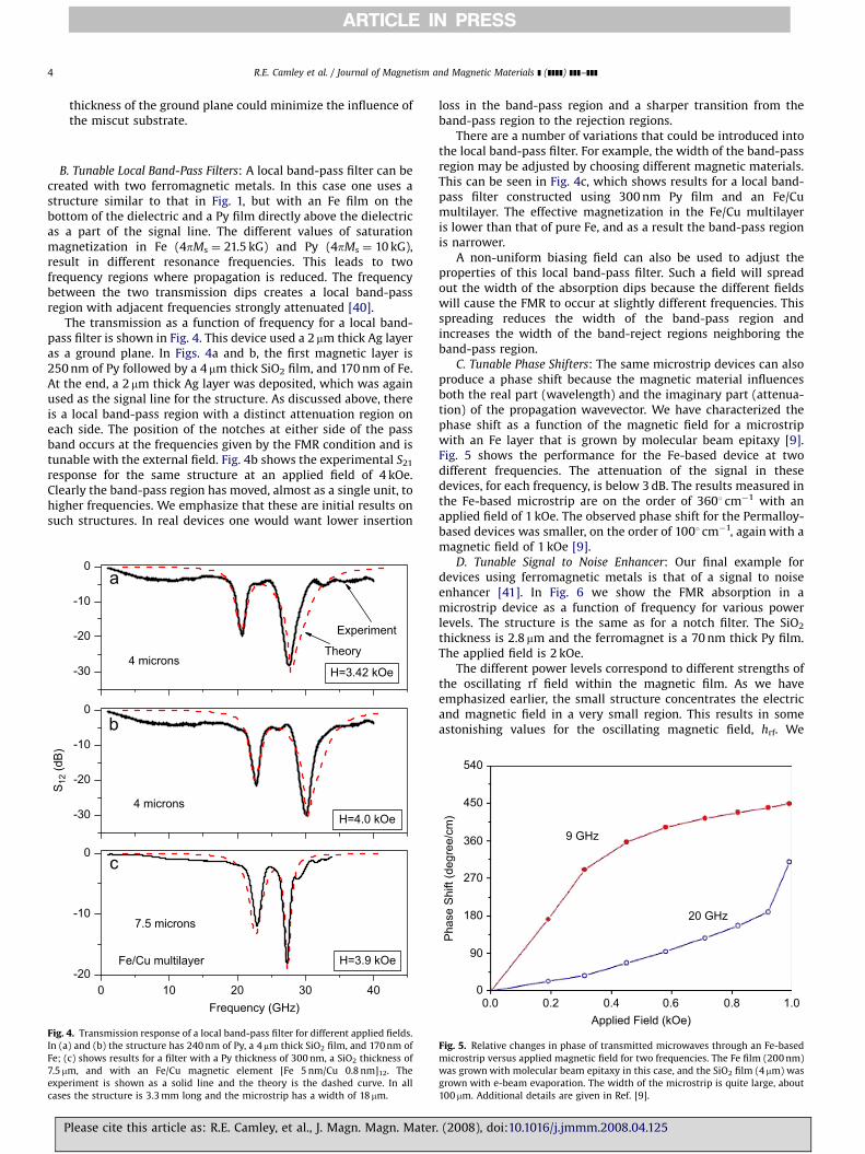
C. Tunable Phase Shifters: The same microstrip devices can alsoproduce a phase shift because the magnetic material influencesboth the real part (wavelength) and the imaginary part (attenua-tion) of the propagation wavevector. We have characterized thephase shift as a function of the magnetic field for a microstripwith an Fe layer that is grown by molecular beam epitaxy [9].Fig. 5 shows the performance for the Fe-based device at twodifferent frequencies. The attenuation of the signal in thesedevices, for each frequency, is below 3 dB. The results measured inthe Fe-based microstrip are on the order of 3601 cm�1 with anapplied field of 1 kOe. The observed phase shift for the Permalloy-based devices was smaller, on the order of 1001 cm�1, again with amagnetic field of 1 kOe [9].
D. Tunable Signal to Noise Enhancer: Our final example fordevices using ferromagnetic metals is that of a signal to noiseenhancer [41]. In Fig. 6 we show the FMR absorption in amicrostrip device as a function of frequency for various powerlevels. The structure is the same as for a notch filter. The SiO2
thickness is 2.8 mm and the ferromagnet is a 70 nm thick Py film.The applied field is 2 kOe.
The different power levels correspond to different strengths ofthe oscillating rf field within the magnetic film. As we haveemphasized earlier, the small structure concentrates the electricand magnetic field in a very small region. This results in someastonishing values for the oscillating magnetic field, hrf. We
540
450
360
270
180
90
00.0 0.2 0.4 0.6 0.8 1.0
Applied Field (kOe)
Pha
se S
hift
(deg
ree/
cm)
9 GHz
20 GHz
Fig. 5. Relative changes in phase of transmitted microwaves through an Fe-based
microstrip versus applied magnetic field for two frequencies. The Fe film (200 nm)
was grown with molecular beam epitaxy in this case, and the SiO2 film (4mm) was
grown with e-beam evaporation. The width of the microstrip is quite large, about
100 mm. Additional details are given in Ref. [9].
. (2008), doi:10.1016/j.jmmm.2008.04.125

ARTICLE IN PRESS
12 14 16 180.0
0.2
0.4
0.6
0.8
1.0-1.9 dBm+7.7 dBm+13.6 dBm+19.5 dBm+23.4 dBm+27.2 dBm+31.1 dBm
FMR
abs
orpt
ion
(a.u
.)
Frequency (GHz)
Fig. 6. Normalized power ratio for a microstrip waveguide with a 70 nm Permalloy
film. As the power is increased the relative absorption decreases, thus creating a
signal to noise enhancer which allows strong signals to pass and weak signals to be
absorbed. The SiO2 thickness is 2.8 mm. The applied field is 2 kOe.
30 35 40 45 50 55 60-100
-80
-60
-40
-20
0
5 kOe
1 kOeTran
smis
sion
(dB
/cm
)
Frequency (GHz)
4.0 μm SiO20.5 μm BaM
3 kOe
Fig. 7. Theoretical calculations for transmission as a function of frequency for a
microstrip waveguide constructed with SiO2 and BaM films, for three different
values of the applied field. The applied field is along the c-axis and perpendicular
to the plane of the film; however, propagation of the electromagnetic wave is still
in the plane of the sample.
R.E. Camley et al. / Journal of Magnetism and Magnetic Materials ] (]]]]) ]]]–]]] 5
estimate that at the lower power levels the magnitude of hrf isabout 0.1 Oe, while at the highest levels the value can be as high as500 Oe. (The precise value depends on the details of the structure,particularly the width of the microstrip line and the thickness ofthe dielectric below it.)
With such a large value for hrf the motion of the magnetizationbecomes highly nonlinear, and this is reflected in the powerabsorption shown in Fig. 6 where we plot the power ratio,absorbed power/input power, for different input power levels. Atlow powers one sees a strong absorption at the FMR frequency. Asthe power is increased, the power ratio decreases substantially.Thus if the input to the device consists of low power noise and ahigh power signal, the high power signal will be preferentiallytransmitted, effectively creating a signal to noise enhancer. Similardevices have been made previously with YIG as the active element[42], but these generally operate at lower frequencies, as notedearlier.
46 48 50 52 54
-120
-100
-80
-60
-40
H = 4.92 kOe
H = 5.2 kOe
H = 5.4 kOeTran
smis
sion
(dB
/cm
)
Frequency (GHz)
Fig. 8. Experimental results for a microstrip using a 2mm thick BaM film. The
applied field is perpendicular to the film plane. The data is taken from
measurements on very short lines, 0.86 and 2.15 mm in length.
4. Planar devices with other materials
A key point of much of the earlier material is that the confinedgeometry presents opportunities to explore parameters anddevices that are not as easily produced in large-scale bulkversions. One example of this concerns the use of hexagonalferrites. Hexagonal ferrites have been investigated for many yearsfor use in high-frequency signal processing because they containlarge internal anisotropy fields, which, according to Eq (1), willresult in high-frequency resonance without large external fields[43,44]. Furthermore, these materials are insulators, eliminatingeddy current losses, which can be a problem in the metallicferromagnets.
Despite the advantages of hexagonal ferrites, there are alsoproblems. One such problem is associated with the size of thesamples required for useful signal processing. One often sees inthe literature phrases such as [45] ‘‘These films are potentiallyuseful for thin film millimeter-wave devices such as circulators,isolators, and phase shifters, provided that thick films (e.g.,20–100 mm) y can be grown.’’ This has lead to a significantnumber of explorations of how to grow high-quality thickhexaferrite films. In fact, our theoretical calculations and initial
Please cite this article as: R.E. Camley, et al., J. Magn. Magn. Mater. (
experimental results show that in the small geometries exploredhere, one may be able to make useful devices with M-type Bahexagonal ferrite (BaM) films, which have a thickness of less thana micrometer.
Fig. 7 shows a theoretical calculation for transmission as afunction of frequency for a microstrip device with two materialsbetween the metallic guiding plates [46]. The geometry is similarto that shown in Fig. 1 except that the magnetic field is orientedperpendicular to the interfaces. The thickness of the hexagonalferrite is 0.5 mm and the thickness of the SiO2 spacer is 4.5mm. Theassumed linewidth is 400 Oe at 40 GHz. The results show asubstantial symmetric dip or notch in the transmission, with theposition of the notch tunable with external field. For thisgeometry the maximum transmission loss is about 85 dB/cm.
Fig. 8 shows some initial experimental results for a notch filterconstructed with a BaM film in a microstrip geometry [47]. The
2008), doi:10.1016/j.jmmm.2008.04.125

ARTICLE IN PRESS
0 10 20 30 40 50 60 70-40
-35
-30
-25
-20
-15
-10
-5
0
Pha
se S
hift
(deg
.)
Frequency (GHz)
34 V30 V25 V20 V15 V10 V5 V0 V
Fig. 10. Phase change as a function of frequency for different biasing voltages for a
co-planar waveguide covered with a nematic liquid crystal, E7.
R.E. Camley et al. / Journal of Magnetism and Magnetic Materials ] (]]]]) ]]]–]]]6
thickness of the BaM film is 2mm; the thickness and the width ofthe Cu signal line on the top of the film are 1.6 and 4.5 mm,respectively. The Si substrate is covered by Pt, which serves as theground plane. The key result seen in this figure is that theattenuation at the notch is indeed quite substantial, near 100 dB/cm,as expected from the theoretical calculation shown earlier.Obviously the background attenuation of 30 dB/cm is much toohigh—this is partly due to a lack of a 50O impedance for thestructure—but it is expected that this could be reduced byintroducing a SiO2 film in our structure.
It is, in principle, also possible to use similar devices to operatein a very different frequency range. Signal processing at higherfrequencies, 100 GHz–10 THz, is also of interest for radar andsatellite communication. For these very high frequencies one canemploy antiferromagnetic materials which have resonance fre-quencies in the far infrared region of the spectrum rather than inthe microwave region as for ferromagnets. Also, many of theantiferromagnets are insulators and eddy current losses areminimal as for the hexagonal ferrites.
It is well known that the resonance frequency on a uniaxial
antiferromagnet is given by f ¼ gffiffiffiffiffiffiffiffiffiffiffiffiffiffiffiffiffiffiffiffiffiffiffiffiffiffiffiffiffiHað2He þ HaÞ
pin the absence of
demagnetizing effects and an external field [48]. Here Ha is theanisotropy field, He the exchange field, g the gyromagnetic ratio,and f the frequency.
A theoretical calculation [49] for a tunable notch filter using anantiferromagnet as the active medium shows the followingresults:
(1)
Atte
nuat
ion
(dB
/cm
)
Fig.filter
thick
incre
P
One can obtain significant attenuation (above 35 dB/cm) sothat ultra-small devices with thicknesses on the order of1–10 mm can be made in a planar geometry. The attenuation ofthe electromagnetic wave is strongly influenced by theanisotropy field, with larger Ha values leading to larger lossesat resonance. The absorption can, in fact, be quite large forFeF2 as seen in Fig. 9.
(2)
In contrast to the results for a ferromagnet, the filters with asingle uniaxial antiferromagnet can also be used to provide alocal band-pass region. The width of the band-pass region isproportional to the applied magnetic field as is seen in Fig. 9.We point out that other geometries and other classes ofmaterials may also be of interest for high-frequency signal
1380 1400 1420 1440 1460 14800
220
440
660
880
1100
H0 =10 kG
H0 = 8 kGH0 = 5 kG
H0 =3 kG
Frequency (GHz)
5 micron SiO21 micron FeF2ΔH = 900GMs = 0.56 kGHa = 197 kGHe = 533 kG
9. Theoretical calculations of the attenuation as a function of frequency for a
constructed with an antiferromagnet for different applied fields. SiO2 has a
ness of 5 mm and the FeF2 film has a thickness of 1mm. As the external field is
ased a local band-pass region develops.
lease cite this article as: R.E. Camley, et al., J. Magn. Magn. Mater
processing. One such material is the group of liquid crystals[50,51]. We have, for example, studied the phase shifting proper-ties of these materials in the range 0–70 GHz using a co-planarwaveguide structure. The co-planar waveguide is constructed on aGaAs substrate and has three parallel Cu lines, a central conductorthat is 64mm wide separated from two ground planes by adistance of 42 mm. The Cu thickness was 2 mm. A model nematicliquid crystal E7 is situated directly on top of the co-planarwaveguide. Fig. 10 presents the results for phase shift as a functionof frequency for different biasing voltages between the centralconductor and the ground planes. We see a tunable phase shift ofabout 251 at 70 GHz. Furthermore, the phase shift increasessteadily as the frequency increases and is expected to be evenlarger above 70 GHz. The insertion loss is below 3 dB over thewhole frequency range, and the differential loss is less than 1 dB.
We point out that the phase shift ought to be substantiallylarger in a small microstrip geometry. The reason for this is that inthe co-planar structure the substrate dielectric plays a significantrole in setting the effective dielectric constant for the structure.Thus the change in the effective e due to the orientation of theliquid crystal caused by the electric field is minimized. In amicrostrip structure the substrate is shielded from the device bythe ground plane and one measures the full change in e of theliquid crystal. Some microstrip phase shifters have already beeninvestigated in the range 10–20 GHz [52].
5. Summary and discussion
In this paper, we have examined the properties of a set ofmicrowave devices that use metallic ferromagnets such as Fe andPermalloy as the tunable magnetic element. These devices operatein the 10–40 GHz frequency range and include tunable notchfilters, band-pass filters, phase shifters, and a signal to noiseenhancer. They are grown by techniques such as magnetronsputtering, which are compatible with industrial standards. Thedevices are planar, very small, and can be integrated withmicrowave electronics on a single chip. All of them exhibit asmall insertion loss (2–3 dB) away from the FMR. The notch filtershave high attenuation (60–100 dB/cm) at a frequency that istunable by an external magnetic field.
In addition, we have explored the use of other materials suchas hexagonal ferrites, antiferromagnets, and liquid crystals insimilar geometries. Because of large internal fields, the hexagonal
. (2008), doi:10.1016/j.jmmm.2008.04.125

ARTICLE IN PRESS
R.E. Camley et al. / Journal of Magnetism and Magnetic Materials ] (]]]]) ]]]–]]] 7
ferrites and antiferromagnets can operate at much higherfrequencies ranging from 50 GHz to 1.5 THz. Our theoreticalcalculations and initial experimental work indicate that it ispossible to construct useful devices with films that are on theorder of 1 mm in thickness. The liquid crystal devices showpromise as phase shifters.
We emphasize that the parameters and devices shown herecan be modified by use of different materials or different physicalgeometries. For example, we showed that the operationalfrequency of the devices can be significantly increased by shapeanisotropy or by exchange coupling of one magnetic film toanother. The linewidth of the device can also be altered by using amultilayer structure as shown earlier.
There are several issues which can impact the implementationof these devices:
(1)
Pl
While the magnetic materials exhibit significant operationalfrequency range, they must be tuned by a magnetic field. Aswe have pointed out, the use of ferromagnetic metals andother materials reduces the size of the required field, but it isnot eliminated. We estimate, for example, that a notch filterthat could be tuned over a 10 GHz range would require a smallelectromagnet. This could be done with a weight of about 50 gand 5 W of power. Ideally one would like a tunable, planarmagnet that is on the same chip as the filtering device.
(2)
There are some losses associated with the metallic guides athigh frequencies. For example, our data show that the losseswithin a fixed structure increase substantially as thefrequency increases above 40 GHz. These losses can bereduced by increasing the thickness of the dielectric layer orby increasing the thicknesses of the conducting layers [53].However, this may reduce some of the advantages of thesmall-scale geometry discussed earlier.Acknowledgment
The authors acknowledge support from the DOA Grant No.W911NF-04-1-0247
References
[1] J.D. Adam, L.E. Davis, G.F. Dionne, E.F. Schloemann, S.N. Stitzer, IEEE Trans.Microwave Theory Tech. 50 (2002) 721.
[2] E. Schloemann, R. Tustison, J. Weissman, H.J. Van Hook, T. Varitimos, J. Appl.Phys. 63 (1988) 3140.
[3] V.S. Liau, T. Wong, W. Stacey, S. Ali, E. Schloemann, IEEE MTT-S 3 (1991) 957.[4] C.S. Tsai, J. Su, C.C. Lee, IEEE Trans. Magn. 35 (1999) 3178.[5] R.E. Camley, D.L. Mills, J. Appl. Phys. 82 (1997) 3058.[6] R.J. Astalos, R.E. Camley, J. Appl. Phys. 83 (1998) 3744.[7] B. Kuanr, I.R. Harward, D.L. Marvin, T. Fal, R.E. Camley, D.L. Mills, Z. Celinski,
IEEE Trans. Magn. 41 (2005) 3538.[8] N. Cramer, D. Lucic, R.E. Camley, Z. Celinski, J. Appl. Phys. 87 (2000) 6911.[9] N. Cramer, D. Lucic, D.K. Walker, R.E. Camley, Z. Celinski, IEEE Trans. Magn. 37
(2001) 2392.[10] B. Kuanr, L. Malkinski, R.E. Camley, Z. Celinski, P. Kabos, J. Appl. Phys. 93
(2003) 8591.[11] K.H. Kim, H. Nagura, S. Ohnuma, M. Yamaguchi, K.-I. Arai, J. Appl. Phys. 93
(2003) 8002.
ease cite this article as: R.E. Camley, et al., J. Magn. Magn. Mater. (
[12] K.H. Kim, S. Ohnuma, M. Yamaguchi, IEEE Trans. Magn. 40 (2004) 2838.[13] L. Li, D.W. Lee, M. Mao, T. Schneider, R. Bubber, K.P. Hwang, Y. Min, S.X. Wang,
J. Appl. Phys. 101 (2007) 123912.[14] G. Goglio, S. Pignard, A. Radulescu, L. Piraux, I. Huynen, D.V. Janvier, A.V.
Vorst, Appl. Phys. Lett. 75 (1999) 1769.[15] A. Encinas, M. Demand, L. Vila, L. Piraux, I. Huynen, Appl. Phys. Lett. 81 (2002)
2031.[16] I. Huynen, L. Piraux, D.V. Janvier, A.V. Vorst, in: Proceedings of PIERS 2000
Symposium, July 2000, 323pp.[17] A. Saib, M. Darques, L. Piraux, D.V. Janvier, I. Huynen, J. Phys. D 38 (2005)
2759.[18] B. Ye, F. Li, D. Cimpoesu, J.B. Wiley, J.-S. Jung, A. Stancu, L. Spinu, J. Magn.
Magn. Mater. 316 (2007) e56.[19] Y. Zhuang, B. Rejaei, E. Boellaard, M. Vroubel, J.N. Burghartz, IEEE Microwave
Wireless Components Lett. 12 (2002) 473.[20] P.K. Amiri, B. Rejaei, M. Vroubel, Y. Zhuang, J.N. Burghartz, IEEE Trans. Magn.
43 (2007) 1880.[21] F. Schoenstein, P. Aublanc, H. Pages, S. Queste, V. Barentin, A.-L. Adenot, N.
Mallejac, O. Acher, J. Magn. Magn. Mater. 292 (2005) 201.[22] N. Vukadinovic, O. Vacus, M. Labrune, O. Acher, D. Pain, Phys. Rev. Lett. 85
(2000) 2817.[23] E. Salahun, P. Queffelec, G. Tanne, A.-L. Adenot, O. Acher, J. Appl. Phys 91
(2002) 5449.[24] Y. He, P. He, S.D. Yoon, P.V. Parimi, F.J. Rachford, V.G. Harris, C. Vittoria,
J. Magn. Magn. Mater. 313 (1) (2007) 187.[25] M. Matters-Kammerer, U. Mackens, K. Reimann, R. Pietig, D. Hennings, B.
Schreinemacher, R. Mauczok, S. Gruhlke, C. Martiny, Microelectron. Reliab. 46(2006) 134.
[26] S.-J. Lee, S.E. Moon, M.-H. Kwak, H.-C. Ryu, Y.-T. Kim, K.-Y. Kang, Integr.Ferroelectr. 72 (2005) 39.
[27] G.M. Rebeiz, RFMEMS Theory, Design, and Technology, Wiley, New York,2003.
[28] H.J. De los Santos, RF MEMS Circuit Design, Artech House, Boston, 2002.[29] E. Marsan, J. Gauthier, M. Chaker, K. Wu, in: Proceedings of the Third IEEE-
NEWCAS Conference, 19–22 June 2005, pp. 279–282.[30] G. Srinivasan, A.S. Tatarenko, M.I. Bichurin, Electron. Lett. 41 (2005) 596.[31] R.B. Marks, IEEE Trans. Microwave Theory Tech. 39 (1991) 1205.[32] B. Kuanr, R.E. Camley, Z. Celinski, Appl. Phys. Lett. 83 (2003) 3969.[33] B. Kuanr, R.E. Camley, Z. Celinski, Appl. Phys. Lett. 87 (2005) 012502.[34] B.K. Kuanr, I.R. Harward, R.T. Deiotte, R.E. Camley, Z. Celinski, J. Appl. Phys. 97
(2005) 10Q103.[35] C. Kittel, Phys. Rev. 73 (1948) 155.[36] Y.V. Khivintsev, B.K. Kuanr, I. Harward, R.E. Camley, Z. Celinski, J. Appl. Phys.
99 (2006) 08P512.[37] M. Grimsditch, R. Camley, E.E. Fullerton, S. Jiang, S.D. Bader, C.H. Sowers, J.
Appl. Phys 85 (1999) 5901.[38] R.J. Astalos, R.E. Camley, Phys. Rev. B 58 (1998) 8646.[39] B.K. Kuanr, Y.V. Khivintsev, I. Harward, R.E. Camley, Z.J. Celinski, M.
Bedenbecker, H.H. Gatzen, IEEE Trans. Magn 43 (2007) 2648.[40] B.K. Kuanr, D.L. Marvin, T.M. Christensen, R.E. Camley, Z. Celinski, Appl. Phys.
Lett. 87 (2005) 222506.[41] Y. Khivintsev, V. Zagorodnii, A. Hutchison, R. Camley, Z. Celinski, Appl. Phys.
Lett. 92 (2008) 022512.[42] J.D. Adam, S.N. Stiltzer, Appl. Phys. Lett. 36 (1980) 485.[43] Y.-Y. Songa, S. Kalarickal, C.E. Patton, J. Appl. Phys. 94 (2003) 5103.[44] Y. Chen, A.L. Geiler, T. Chen, T. Sakai, C. Vittoria, V.G. Harris, J. Appl. Phys. 101
(2007) 09M501.[45] P.C. Dorsey, D.B. Chrisey, J.S. Horwitz, P. Lubitz, R.C.Y. Auyeung, IEEE Trans.
Magn. 30 (1994) 4512.[46] T. Fal, R.E. Camley, J. Appl. Physics, in press.[47] V.V. Zagorodnii, Y.V. Khivintsev, S.D. Yoon, Yajir Chen, R.E. Camley, Z. Celinski,
C. Vittoria, V.G. Harris, unpublished.[48] C. Kittel, Introduction to Solid State Physics, fourth ed., Wiley, New York, 1971,
p. 603.[49] V. Veerakumar, R.E. Camley, J. Appl. Phys. 101 (2007) 093906.[50] C. Weil, St. Muller, P. Scheele, P. Best, G. Lussem, R. Jakoby, Electron. Lett. 39
(2003) 1732.[51] D. Dolfi, M. Labeyrie, P. Joffre, J.P. Huignard, Electron. Lett. 29 (1993) 926.[52] C. Weil, G. Luessem, R. Jakoby, IEEE MTT-S Dig. 367 (2002) 1.[53] R.A. Pucel, D.J. Masse, C.P. Hartwig, IEEE Trans. Microwave Theory Tech. MTT-
16 (1968) 342.
2008), doi:10.1016/j.jmmm.2008.04.125